Embed Size (px)
Citation preview
Publication# 16492 Rev. D Amendment /0
Issue Date: February 1996 2-3
AdvancedMicro
Devices
PAL16R8 Family20-Pin TTL Programmable Array Logic
FINAL COM’L: -4/5/7/B/B-2/A, D/2
DISTINCTIVE CHARACTERISTICS As fast as 4.5 ns maximum propagation delay
Popular 20-pin architectures: 16L8, 16R8, 16R6,16R4
Programmable replacement for high-speed TTLlogic
Register preload for testability
Power-up reset for initialization
Extensive third-party software and programmersupport through FusionPLD partners
20-Pin DIP and PLCC packages save space
28-Pin PLCC-4 package provides ultra-cleanhigh-speed signals
GENERAL DESCRIPTIONThe PAL16R8 Family (PAL16L8, PAL16R8, PAL16R6,PAL16R4) includes the PAL16R8-5/4 Series which pro-vides the highest speed in the 20-pin TTL PAL devicefamily, making the series ideal for high-performance ap-plications. The PAL16R8 Family is provided with stan-dard 20-pin DIP and PLCC pinouts and a 28-pin PLCCpinout. The 28-pin PLCC pinout contains seven extraground pins interleaved between the outputs to reducenoise and increase speed.
The devices provide user-programmable logic for re-placing conventional SSI/MSI gates and flip-flops at areduced chip count.
The family allows the systems engineer to implementthe design on-chip, by opening fuse links to configureAND and OR gates within the device, according to thedesired logic function. Complex interconnections be-tween gates, which previously required time-consuminglayout, are lifted from the PC board and placed on sili-con, where they can be easily modified during proto-typing or production.
The PAL device implements the familiar Boolean logictransfer function, the sum of products. The PAL deviceis a programmable AND array driving a fixed OR array.
The AND array is programmed to create custom productterms, while the OR array sums selected terms at theoutputs.
In addition, the PAL device provides the followingoptions:
— Variable input/output pin ratio
— Programmable three-state outputs
— Registers with feedback
Product terms with all connections opened assume thelogical HIGH state; product terms connected to both trueand complement of any single input assume the logicalLOW state. Registers consist of D-type flip-flops that areloaded on the LOW-to-HIGH transition of the clock. Un-used input pins should be tied to VCC or GND.
The entire PAL device family is supported by theFusionPLD partners. The PAL family is programmed onconventional PAL device programmers with appropriatepersonality and socket adapter modules. Once the PALdevice is programmed and verified, an additional con-nection may be opened to prevent pattern readout. Thisfeature secures proprietary circuits.
PRODUCT SELECTOR GUIDE
Dedicated Product Terms/Device Inputs Outputs Output Feedback Enable
PAL16L8 10 6 comb. 7 I/O prog.2 comb. 7 – prog.
PAL16R8 8 8 reg. 8 reg. pin
PAL16R6 8 6 reg. 8 reg. pin2 comb. 7 I/O prog.
PAL16R4 8 4 reg. 8 reg. pin4 comb. 7 I/O prog.
AMD
2-4 PAL16R8 Family
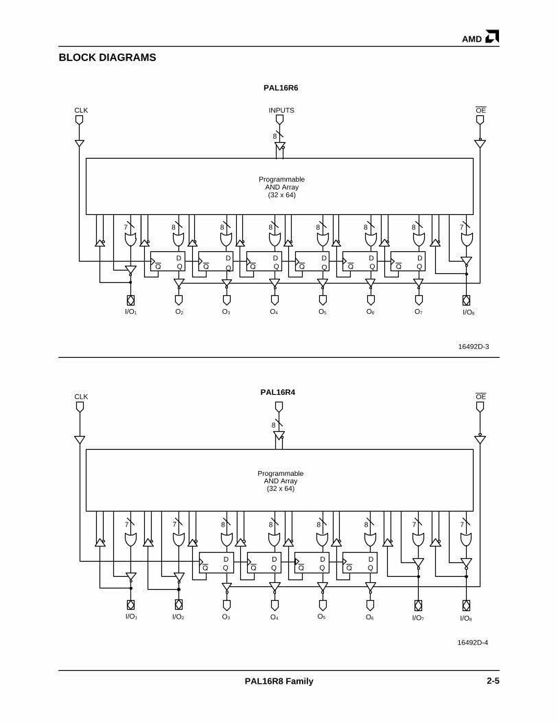
BLOCK DIAGRAMS
16492D-1
77
ProgrammableAND Array(32 x 64)
PAL16L8
10
INPUTS
O1 I/O2 I/O3 I/O4 I/O5 I/O6 I/O7 O8
7 7 7 7 7 7
16492D-2
8 8
O2 O3 O4 O5 O6 O7 O8
DQQ
O1
ProgrammableAND Array(32 x 64)
PAL16R8
8
INPUTS OECLK
DQQ
DQQ
DQQ
DQQ
DQQ
DQQ
DQQ
88 8 8 88
AMD
2-5PAL16R8 Family
BLOCK DIAGRAMS
16492D-3
7 8888
ProgrammableAND Array(32 x 64)
8
INPUTS OECLK
PAL16R6
O2 O3 O4 O5 O6 O7 I/O8
QQQ QDQ
8 8 7
I/O1
QD
QD
QD
QD
Q QD
Q
DQ
7
Q
ProgrammableAND Array(32 x 64)
OECLK
I/O1
8
PAL16R4
I/O2 I/O7 I/O8O3 O4 O5 O6
DQQ
DQQ
DQQ
8 8 8 8 777
16492D-4
AMD
2-6 PAL16R8 Family
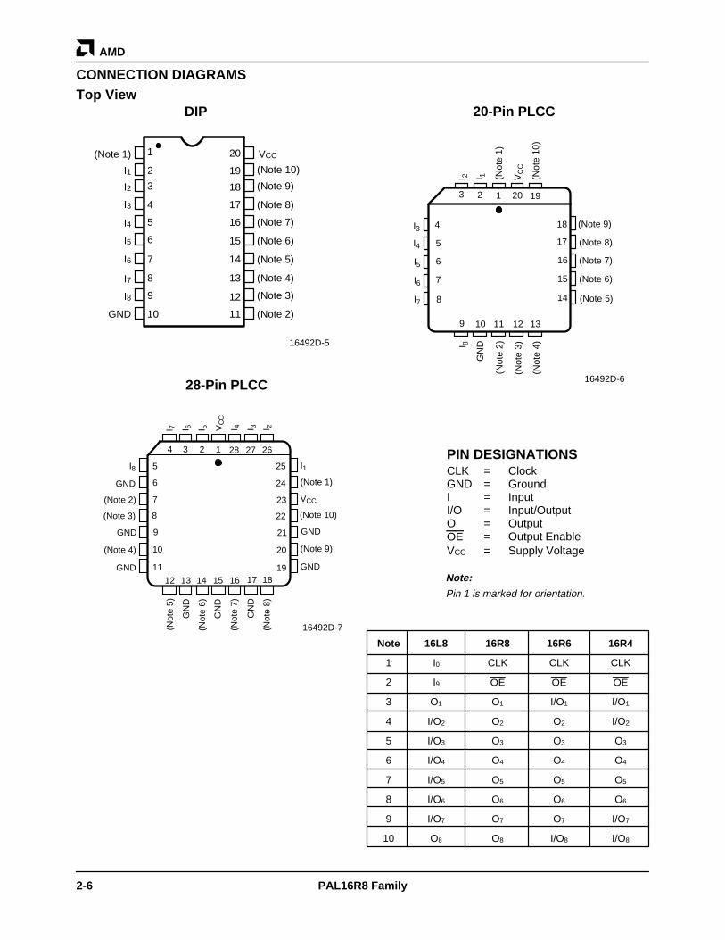
CONNECTION DIAGRAMSTop View
1234 28 27 26
255
24
23
22
21
20
1918171615
6
7
8
9
10
11
12 13 14
I8
GND
(Note 2)
(Note 3)
GND
(Note 4)
GND
I1
(Note 1)
VCC
(Note 10)
GND
(Note 9)
GND
(Not
e 8)
GN
D
(Not
e 7)
GN
D
(Not
e 5)
GN
D
(Not
e 6)
VC
C
I 5I 6I 7 I 4 I 3 I 2
1 20 19
18
17
16
15
14
23
4
5
6
7
8
9 10 11 12 13
I3
I4
I5
I6
I7
(Note 9)
(Note 8)
(Note 7)
(Note 6)
(Note 5)
(Not
e 2)
(Not
e 3)
(Not
e 4)
GN
DI 8
(Not
e 1)
VC
C
(Not
e 10
)
I 1I 2
16
14
12
13
19
Note 16L8 16R8 16R6 16R4
1 I0 CLK CLK CLK
2 I9 OE OE OE
3 O1 O1 I/O1 I/O1
4 I/O2 O2 O2 I/O2
5 I/O3 O3 O3 O3
6 I/O4 O4 O4 O4
7 I/O5 O5 O5 O5
8 I/O6 O6 O6 O6
9 I/O7 O7 O7 I/O7
10 O8 O8 I/O8 I/O8
PIN DESIGNATIONSCLK = ClockGND = GroundI = InputI/O = Input/OutputO = OutputOE = Output EnableVCC = Supply Voltage
DIP 20-Pin PLCC
(Note 1)
(Note 10)I1
I2
I3
I4
I5
I6
I7
GND
I8
(Note 9)
(Note 8)
(Note 7)
(Note 5)
(Note 4)
(Note 3)
(Note 2)
VCC
(Note 6)
28-Pin PLCC
Note:
Pin 1 is marked for orientation.
16492D-5
16492D-6
16492D-7
3
5
7
2
1
4
8
6 15
11
9
10
17
18
20
AMD
2-7PAL16R8-4/5/7, D/2 (Com’l)
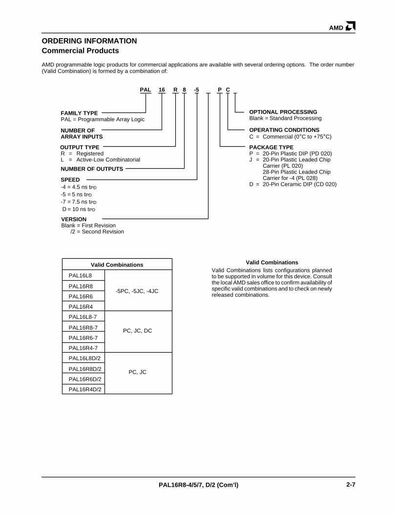
ORDERING INFORMATIONCommercial Products
AMD programmable logic products for commercial applications are available with several ordering options. The order number(Valid Combination) is formed by a combination of:
Valid CombinationsValid Combinations lists configurations plannedto be supported in volume for this device. Consultthe local AMD sales office to confirm availability ofspecific valid combinations and to check on newlyreleased combinations.
PAL 16 R 8 -5 P C
FAMILY TYPEPAL = Programmable Array Logic
NUMBER OF ARRAY INPUTS
OUTPUT TYPER = RegisteredL = Active-Low Combinatorial
NUMBER OF OUTPUTS
SPEED-4 = 4.5 ns tPD
-5 = 5 ns tPD
-7 = 7.5 ns tPD
D = 10 ns tPD
PACKAGE TYPEP = 20-Pin Plastic DIP (PD 020)J = 20-Pin Plastic Leaded Chip
Carrier (PL 020)28-Pin Plastic Leaded Chip Carrier for -4 (PL 028)
D = 20-Pin Ceramic DIP (CD 020)
OPERATING CONDITIONSC = Commercial (0°C to +75°C)
OPTIONAL PROCESSINGBlank = Standard Processing
PAL16L8
-5PC, -5JC, -4JC
Valid Combinations
PAL16R8
PAL16R6
PAL16R4
PAL16L8-7
PAL16R8-7
PAL16R6-7
PAL16R4-7
PC, JC, DC
VERSIONBlank = First Revision /2 = Second Revision
PAL16L8D/2
PAL16R8D/2
PAL16R6D/2
PAL16R4D/2
PC, JC
AMD
2-8 PAL16R8/B/B-2/A/B-4 (Com’l)
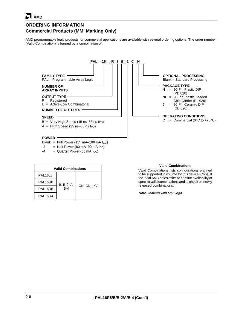
ORDERING INFORMATIONCommercial Products (MMI Marking Only)
h. PACKAGE TYPEN = 20-Pin Plastic DIP
(PD 020)NL = 20-Pin Plastic Leaded
Chip Carrier (PL 020)J = 20-Pin Ceramic DIP
(CD 020)
AMD programmable logic products for commercial applications are available with several ordering options. The order number(Valid Combination) is formed by a combination of:
PAL16L8
Valid CombinationsValid Combinations
Valid Combinations lists configurations plannedto be supported in volume for this device. Consultthe local AMD sales office to confirm availability ofspecific valid combinations and to check on newlyreleased combinations.
Note: Marked with MMI logo.
PAL 16 R 8 B C N
PAL16R8
PAL16R6
PAL16R4
a. FAMILY TYPEPAL = Programmable Array Logic
b. NUMBER OF ARRAY INPUTS
c. OUTPUT TYPER = RegisteredL = Active-Low Combinatorial
d. NUMBER OF OUTPUTS
SPEEDB = Very High Speed (15 ns–35 ns tPD)A = High Speed (25 ns–35 ns tPD)
g. OPERATING CONDITIONSC = Commercial (0°C to +75°C)
i. OPTIONAL PROCESSINGBlank = Standard Processing
-2
f. POWERBlank = Full Power (155 mA–180 mA ICC)-2 = Half Power (80 mA–90 mA ICC)-4 = Quarter Power (55 mA ICC)
CN, CNL, CJB, B-2, A,B-4
AMD
2-9PAL16R8 Family
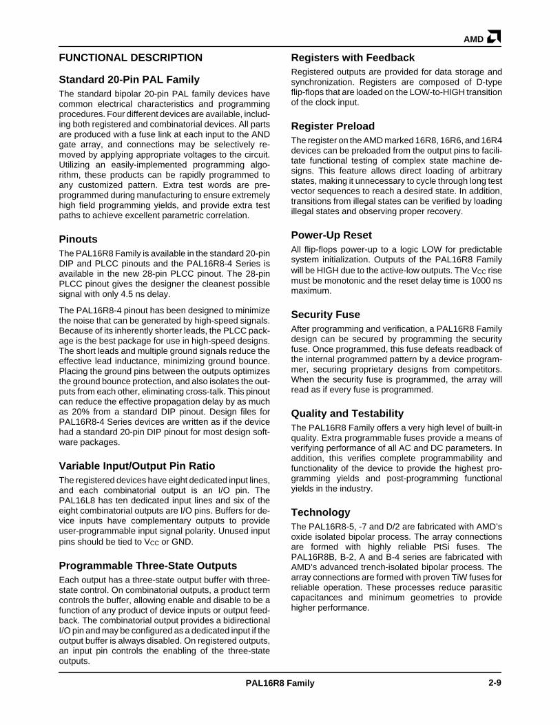
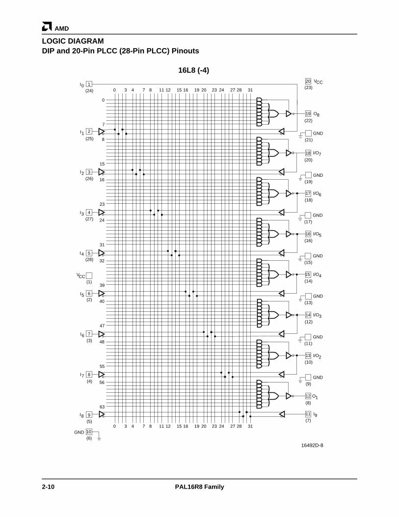
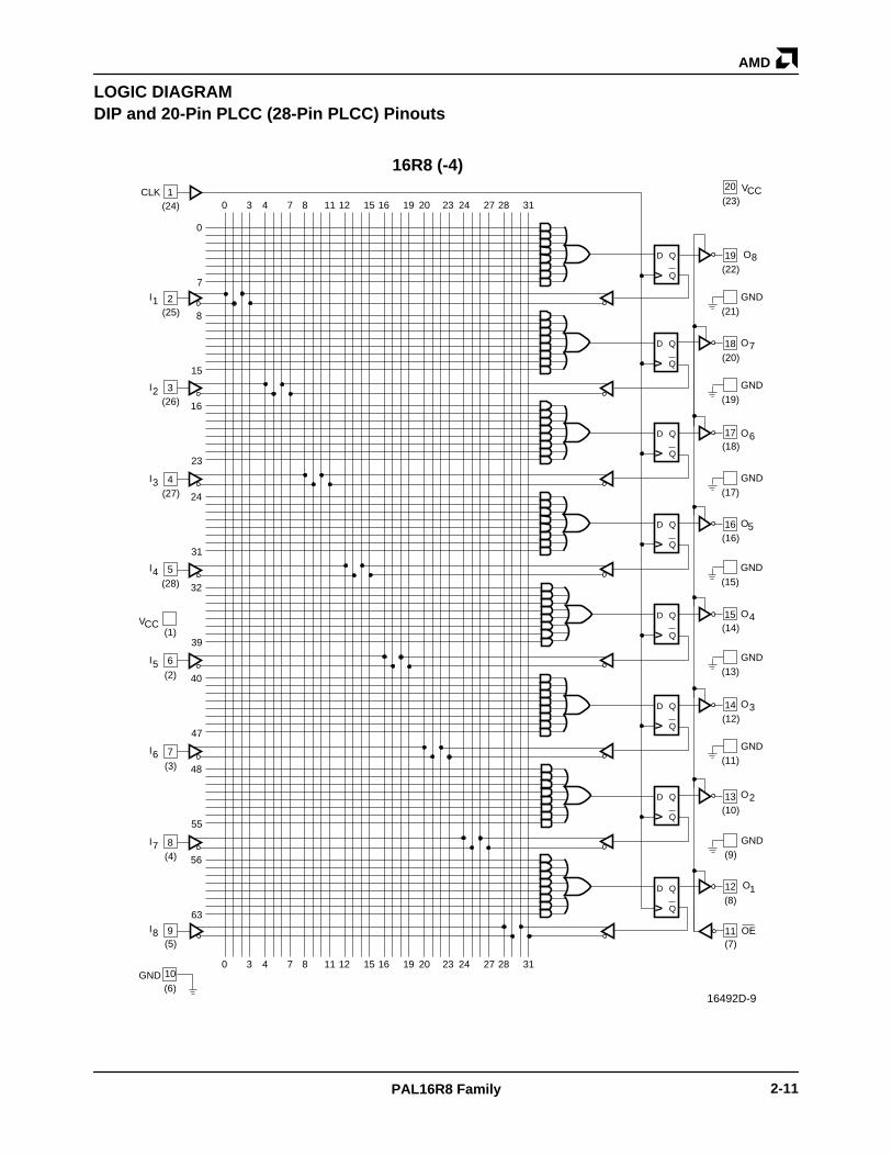
FUNCTIONAL DESCRIPTION
Standard 20-Pin PAL FamilyThe standard bipolar 20-pin PAL family devices havecommon electrical characteristics and programmingprocedures. Four different devices are available, includ-ing both registered and combinatorial devices. All partsare produced with a fuse link at each input to the ANDgate array, and connections may be selectively re-moved by applying appropriate voltages to the circuit.Utilizing an easily-implemented programming algo-rithm, these products can be rapidly programmed toany customized pattern. Extra test words are pre-programmed during manufacturing to ensure extremelyhigh field programming yields, and provide extra testpaths to achieve excellent parametric correlation.
PinoutsThe PAL16R8 Family is available in the standard 20-pinDIP and PLCC pinouts and the PAL16R8-4 Series isavailable in the new 28-pin PLCC pinout. The 28-pinPLCC pinout gives the designer the cleanest possiblesignal with only 4.5 ns delay.
The PAL16R8-4 pinout has been designed to minimizethe noise that can be generated by high-speed signals.Because of its inherently shorter leads, the PLCC pack-age is the best package for use in high-speed designs.The short leads and multiple ground signals reduce theeffective lead inductance, minimizing ground bounce.Placing the ground pins between the outputs optimizesthe ground bounce protection, and also isolates the out-puts from each other, eliminating cross-talk. This pinoutcan reduce the effective propagation delay by as muchas 20% from a standard DIP pinout. Design files forPAL16R8-4 Series devices are written as if the devicehad a standard 20-pin DIP pinout for most design soft-ware packages.
Variable Input/Output Pin RatioThe registered devices have eight dedicated input lines,and each combinatorial output is an I/O pin. ThePAL16L8 has ten dedicated input lines and six of theeight combinatorial outputs are I/O pins. Buffers for de-vice inputs have complementary outputs to provideuser-programmable input signal polarity. Unused inputpins should be tied to VCC or GND.
Programmable Three-State OutputsEach output has a three-state output buffer with three-state control. On combinatorial outputs, a product termcontrols the buffer, allowing enable and disable to be afunction of any product of device inputs or output feed-back. The combinatorial output provides a bidirectionalI/O pin and may be configured as a dedicated input if theoutput buffer is always disabled. On registered outputs,an input pin controls the enabling of the three-stateoutputs.
Registers with FeedbackRegistered outputs are provided for data storage andsynchronization. Registers are composed of D-typeflip-flops that are loaded on the LOW-to-HIGH transitionof the clock input.
Register PreloadThe register on the AMD marked 16R8, 16R6, and 16R4devices can be preloaded from the output pins to facili-tate functional testing of complex state machine de-signs. This feature allows direct loading of arbitrarystates, making it unnecessary to cycle through long testvector sequences to reach a desired state. In addition,transitions from illegal states can be verified by loadingillegal states and observing proper recovery.
Power-Up ResetAll flip-flops power-up to a logic LOW for predictablesystem initialization. Outputs of the PAL16R8 Familywill be HIGH due to the active-low outputs. The VCC risemust be monotonic and the reset delay time is 1000 nsmaximum.
Security FuseAfter programming and verification, a PAL16R8 Familydesign can be secured by programming the securityfuse. Once programmed, this fuse defeats readback ofthe internal programmed pattern by a device program-mer, securing proprietary designs from competitors.When the security fuse is programmed, the array willread as if every fuse is programmed.
Quality and TestabilityThe PAL16R8 Family offers a very high level of built-inquality. Extra programmable fuses provide a means ofverifying performance of all AC and DC parameters. Inaddition, this verifies complete programmability andfunctionality of the device to provide the highest pro-gramming yields and post-programming functionalyields in the industry.
TechnologyThe PAL16R8-5, -7 and D/2 are fabricated with AMD’soxide isolated bipolar process. The array connectionsare formed with highly reliable PtSi fuses. ThePAL16R8B, B-2, A and B-4 series are fabricated withAMD’s advanced trench-isolated bipolar process. Thearray connections are formed with proven TiW fuses forreliable operation. These processes reduce parasiticcapacitances and minimum geometries to providehigher performance.
AMD
2-10 PAL16R8 Family
LOGIC DIAGRAMDIP and 20-Pin PLCC (28-Pin PLCC) Pinouts
16492D-8
0 3 4 7 8 11 12 15 16 19 20 23 24 27 28 31
0
7
0 3 4 7 8 11 12 15 16 19 20 23 24 27 28 31
8
15
16
23
24
31
32
39
40
47
48
55
56
63
I 0
I 1
I 3
I 4
I 5
I 6
I 7
I 8
I 2
O 8
I/O 7
I/O 6
I/O 5
I/O 4
I/O 3
I/O 2
O 1
11 I 9
GND
V CC 1
2
3
4
5
6
7
8
9
12
13
14
16
17
18
19
(24)
(25)
(26)
(27)
(28)
V CC (1)
(2)
(3)
(4)
(5)
(6)
(22)
(21)
(20)
(18)
(16)
(14)
(12)
(10)
(8)
(7)
GND
(19)
GND
(17)
GND
(15)
GND
15
(13)
GND
(11)
GND
(9)
GND
(23) 20
16L8-5 (-4)
10
16L8 (-4)
AMD
2-11PAL16R8 Family
LOGIC DIAGRAMDIP and 20-Pin PLCC (28-Pin PLCC) Pinouts
16492D-9
0 3 4 7 8 11 12 15 16 19 20 23 24 27 28 31
0
7
0 3 4 7 8 11 12 15 16 19 20 23 24 27 28 31
8
15
16
23
24
31
32
39
40
47
48
55
56
63
16R8-5 (-4)
2
3
4
5
6
7
8
9
1
18 D Q
Q
19
17
16
15
14
13
12
11
O 8
O 7
O 6
O 5
O 4
O 3
O 2
O 1
OE
V
CLK
I 1
I 2
I 3
I 4
I 5
I 6
I 7
I 8
D Q
Q V
D Q
Q V
D Q
Q V
D Q
Q V
D Q
Q V
D Q
Q V
D Q
Q V
GND
V CC
(21)
GND
(23)
(22)
(20)
(17)
GND
(18)
(16)
(15)
GND
(14)
GND (11)
(12)
GND (13)
(10)
GND (9)
(8)
(7)
(6)
(5)
(4)
(3)
(2)
V CC (1)
(28)
(27)
(26)
(25)
(24)
(19)
GND
10
20
16R8 (-4)
AMD
2-12 PAL16R8 Family
LOGIC DIAGRAMDIP and 20-Pin PLCC (28-Pin PLCC) Pinouts
0 3 4 7 8 11 12 15 16 19 20 23 24 27 28 31
0
7
0 3 4 7 8 11 12 15 16 19 20 23 24 27 28 31
8
15
16
23
24
31
32
39
40
47
48
55
56
63
16R6-5 (-4)
2
3
4
6
7
9
10
1
18 D Q
Q
19
17
16
15
14
13
12
11
I/O 8
O 7
O 6
O 5
O 4
O 3
O 2
I/O 1
OE
V
CLK
I 1
I 2
I 3
I 4
I 5
I 6
I 7
I 8
D Q
Q V
D Q
Q V
D Q
Q V
D Q
Q V
D Q
Q V
GND
(22)
V CC (23)
(17)
GND
(21)
GND
(20)
(18)
(19)
GND
(16)
(15)
GND
(14)
(13)
GND
(12)
(11)
GND
(10)
(9)
GND
(8)
(7)
V CC (1)
(28) 5
(6)
(5)
(4)
(3)
(2)
(27)
(26)
(25)
(24)
8
20 16R6 (-4)
16492D-10
AMD
2-13PAL16R8 Family
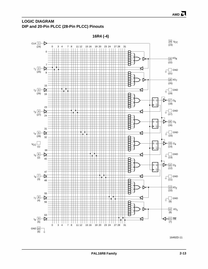
LOGIC DIAGRAMDIP and 20-Pin PLCC (28-Pin PLCC) Pinouts
0 3 4 7 8 11 12 15 16 19 20 23 24 27 28 31
0
7
0 3 4 7 8 11 12 15 16 19 20 23 24 27 28 31
8
15
16
23
24
31
32
39
40
47
48
55
56
63
16R4-5 (-4)
1 CLK
I 1
I 3
I 4
I 5
I 6
I 7
I 8
I 2
I/O 8
I/O 7
O 6
O 5
O 4
O 3
I/O 2
I/O 1
OE
GND
V CC
2
3
4
5
6
7
8
9 11
12
13
14
15
16
17
18
19
D Q
Q V
D Q
Q V
D Q
Q V
D Q
Q V
(6)
(19)
GND
(23)
(22)
(20)
(21)
GND
(18)
(17)
GND
(16)
(14)
GND (15)
GND (13)
(12)
GND (11)
(10)
GND (9)
(8)
(7) (5)
(4)
(3)
(2)
V CC (1)
(28)
(27)
(26)
(25)
(24)
10
20
16R4 (-4)
16492D-11
AMD
2-14 PAL16R8-4/5 (Com’l)
ParameterSymbol Parameter Description Test Conditions Min Max Unit
VOH Output HIGH Voltage IOH = –3.2 mA VIN = VIH or VIL 2.4 VVCC = Min
VOL Output LOW Voltage IOL = 24 mA VIN = VIH or VIL 0.5 VVCC = Min
VIH Input HIGH Voltage Guaranteed Input Logical HIGH 2.0 VVoltage for all Inputs (Note 1)
VIL Input LOW Voltage Guaranteed Input Logical LOW 0.8 VVoltage for all Inputs (Note 1)
VI Input Clamp Voltage IIN = –18 mA, VCC = Min –1.2 V
IIH Input HIGH Current VIN = 2.7 V, VCC = Max (Note 2) 25 µA
IIL Input LOW Current VIN = 0.4 V, VCC = Max (Note 2) –250 µA
II Maximum Input Current VIN = 5.5 V, VCC = Max 1 mA
IOZH Off-State Output Leakage VOUT = 2.7 V, VCC = Max 100 µACurrent HIGH VIN = VIH or VIL (Note 2)
IOZL Off-State Output Leakage VOUT = 0.4 V, VCC = Max –100 µACurrent LOW VIN = VIH or VIL (Note 2)
ISC Output Short-Circuit Current VOUT = 0.5 V, VCC = Max (Note 3) –30 –130 mA
ICC Supply Current VIN = 0 V, Outputs Open (IOUT = 0 mA) 210 mAVCC = Max
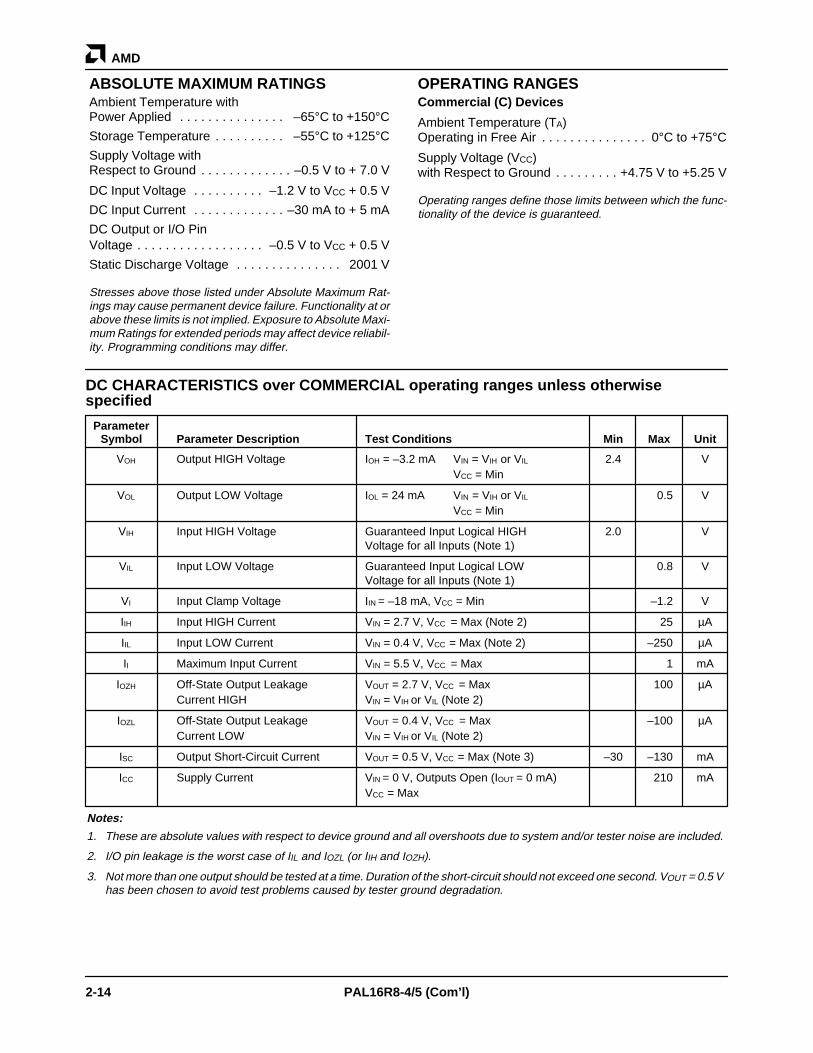
DC CHARACTERISTICS over COMMERCIAL operating ranges unless otherwisespecified
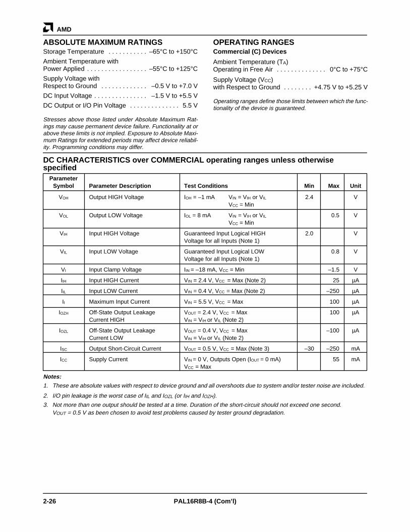
ABSOLUTE MAXIMUM RATINGSAmbient Temperature withPower Applied –65°C to +150°C. . . . . . . . . . . . . . .
Storage Temperature –55°C to +125°C. . . . . . . . . .
Supply Voltage with Respect to Ground –0.5 V to + 7.0 V. . . . . . . . . . . . .
DC Input Voltage –1.2 V to VCC + 0.5 V. . . . . . . . . .
DC Input Current –30 mA to + 5 mA. . . . . . . . . . . . .
DC Output or I/O PinVoltage –0.5 V to VCC + 0.5 V. . . . . . . . . . . . . . . . . .
Static Discharge Voltage 2001 V. . . . . . . . . . . . . . .
Stresses above those listed under Absolute Maximum Rat-ings may cause permanent device failure. Functionality at orabove these limits is not implied. Exposure to Absolute Maxi-mum Ratings for extended periods may affect device reliabil-ity. Programming conditions may differ.
OPERATING RANGESCommercial (C) Devices
Ambient Temperature (TA)Operating in Free Air 0°C to +75°C. . . . . . . . . . . . . . .
Supply Voltage (VCC)with Respect to Ground +4.75 V to +5.25 V. . . . . . . . .
Operating ranges define those limits between which the func-tionality of the device is guaranteed.
Notes:
1. These are absolute values with respect to device ground and all overshoots due to system and/or tester noise are included.
2. I/O pin leakage is the worst case of IIL and IOZL (or IIH and IOZH).
3. Not more than one output should be tested at a time. Duration of the short-circuit should not exceed one second. VOUT = 0.5 Vhas been chosen to avoid test problems caused by tester ground degradation.
AMD
2-15PAL16R8-4/5 (Com’l)
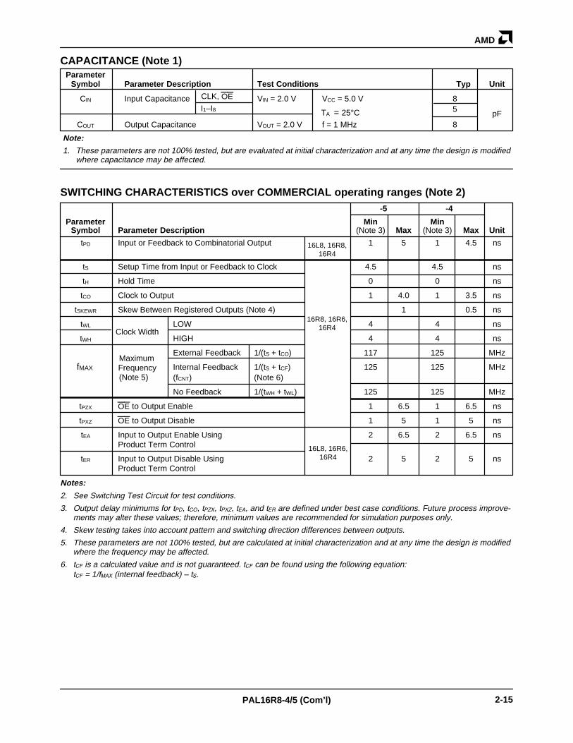
ParameterSymbol Parameter Description Test Conditions Typ Unit
CIN Input Capacitance VIN = 2.0 V VCC = 5.0 V 85
COUT Output Capacitance VOUT = 2.0 V f = 1 MHz 8
Note:
1. These parameters are not 100% tested, but are evaluated at initial characterization and at any time the design is modifiedwhere capacitance may be affected.
Parameter Min MinSymbol Parameter Description (Note 3) Max (Note 3) Max Unit
tPD Input or Feedback to Combinatorial Output 1 5 1 4.5 ns
tS Setup Time from Input or Feedback to Clock 4.5 4.5 ns
tH Hold Time 0 0 ns
tCO Clock to Output 1 4.0 1 3.5 ns
tSKEWR Skew Between Registered Outputs (Note 4) 1 0.5 ns
tWL LOW 4 4 ns
tWH HIGH 4 4 ns
External Feedback 1/(tS + tCO) 117 125 MHz
Internal Feedback 1/(tS + tCF) 125 125 MHz(fCNT) (Note 6)
No Feedback 1/(tWH + tWL) 125 125 MHz
tPZX OE to Output Enable 1 6.5 1 6.5 ns
tPXZ OE to Output Disable 1 5 1 5 ns
tEA Input to Output Enable Using 2 6.5 2 6.5 nsProduct Term Control
tER Input to Output Disable Using 2 5 2 5 nsProduct Term Control
CAPACITANCE (Note 1)
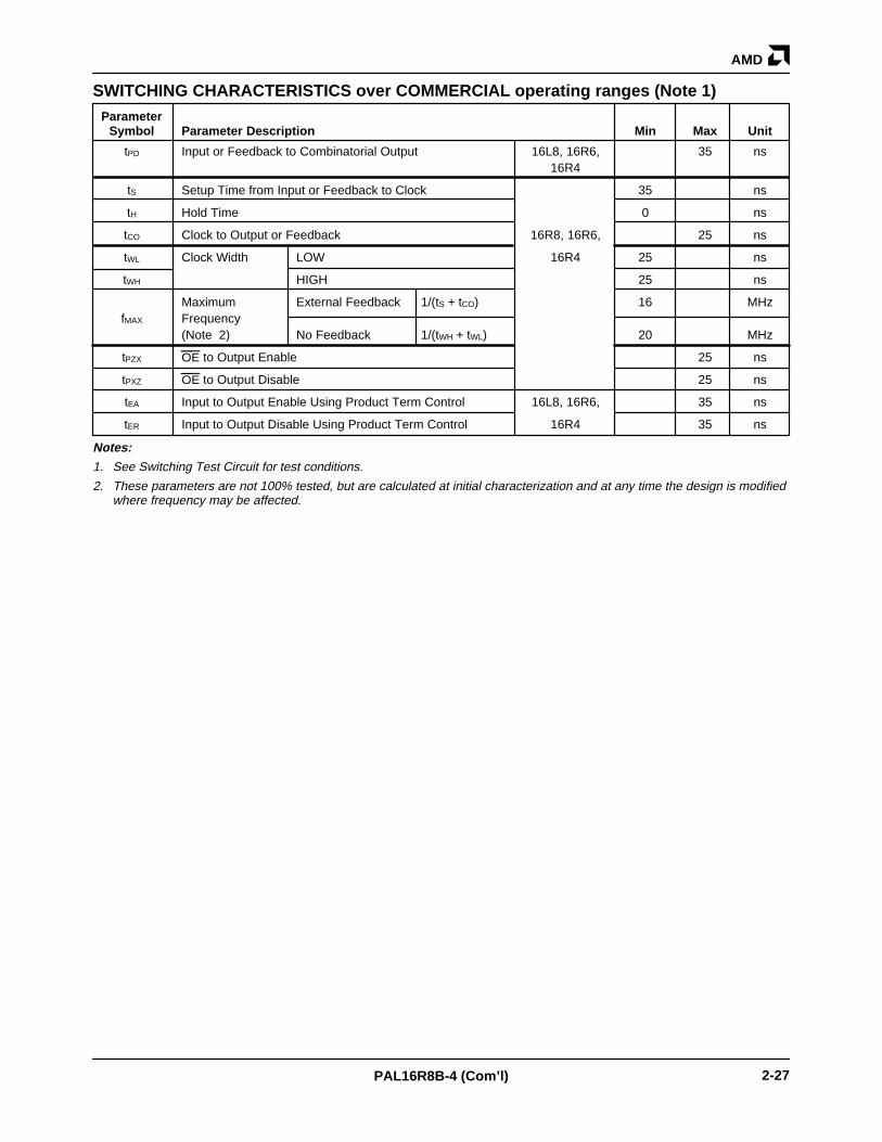
SWITCHING CHARACTERISTICS over COMMERCIAL operating ranges (Note 2)
TA = 25°C pF
Clock Width
MaximumFrequency(Note 5)
fMAX
-5 -4
Notes:
2. See Switching Test Circuit for test conditions.
3. Output delay minimums for tPD, tCO, tPZX, tPXZ, tEA, and tER are defined under best case conditions. Future process improve-ments may alter these values; therefore, minimum values are recommended for simulation purposes only.
4. Skew testing takes into account pattern and switching direction differences between outputs.
5. These parameters are not 100% tested, but are calculated at initial characterization and at any time the design is modifiedwhere the frequency may be affected.
6. tCF is a calculated value and is not guaranteed. tCF can be found using the following equation: tCF = 1/fMAX (internal feedback) – tS.
16R8, 16R6,16R4
16L8, 16R6,16R4
16L8, 16R8,16R4
CLK, OE
I1–I8

AMD
2-16 PAL16R8-7 (Com’l)
ABSOLUTE MAXIMUM RATINGSStorage Temperature –65°C to +150°C. . . . . . . . . . .
Ambient Temperature withPower Applied –55°C to +125°C. . . . . . . . . . . . . . . . .
Supply Voltage with Respect to Ground –0.5 V to + 7.0 V. . . . . . . . . . . . .
DC Input Voltage –1.2 V to + 7.0 V. . . . . . . . . . . . . . .
DC Input Current –30 mA to + 5 mA. . . . . . . . . . . . . .
DC Output or I/O Pin Voltage –0.5 V to VCC + 0.5 V. . . . . . . . . . . . . . . . . .
Static Discharge Voltage 2001 V. . . . . . . . . . . . . . . . .
Stresses above those listed under Absolute Maximum Rat-ings may cause permanent device failure. Functionality at orabove these limits is not implied. Exposure to Absolute Maxi-mum Ratings for extended periods may affect device reliabil-ity. Programming conditions may differ.
OPERATING RANGESCommercial (C) Devices
Ambient Temperature (TA)Operating in Free Air 0°C to +75°C. . . . . . . . . . . . . .
Supply Voltage (VCC)with Respect to Ground +4.75 V to +5.25 V. . . . . . . .
Operating ranges define those limits between which the func-tionality of the device is guaranteed.
DC CHARACTERISTICS over COMMERCIAL operating ranges unless otherwisespecified
ParameterSymbol Parameter Description Test Conditions Min Max Unit
VOH Output HIGH Voltage IOH = –3.2 mA VIN = VIH or VIL 2.4 VVCC = Min
VOL Output LOW Voltage IOL = 24 mA VIN = VIH or VIL 0.5 VVCC = Min
VIH Input HIGH Voltage Guaranteed Input Logical HIGH 2.0 VVoltage for all Inputs (Note 1)
VIL Input LOW Voltage Guaranteed Input Logical LOW 0.8 VVoltage for all Inputs (Note 1)
VI Input Clamp Voltage IIN = –18 mA, VCC = Min –1.2 V
IIH Input HIGH Current VIN = 2.7 V, VCC = Max (Note 2) 25 µA
IIL Input LOW Current VIN = 0.4 V, VCC = Max (Note 2) –250 µA
II Maximum Input Current VIN = 5.5 V, VCC = Max 1 mA
IOZH Off-State Output Leakage VOUT = 2.7 V, VCC = Max 100 µACurrent HIGH VIN = VIH or VIL (Note 2)
IOZL Off-State Output Leakage VOUT = 0.4 V, VCC = Max –100 µACurrent LOW VIN = VIH or VIL (Note 2)
ISC Output Short-Circuit Current VOUT = 0.5 V, VCC = Max (Note 3) –30 –130 mA
ICC Supply Current VIN = 0 V, Outputs Open (IOUT = 0 mA) 180 mAVCC = Max
Notes:
1. These are absolute values with respect to device ground and all overshoots due to system and/or tester noise are included.
2. I/O pin leakage is the worst case of IIL and IOZL (or IIH and IOZH).
3. Not more than one output should be tested at a time. Duration of the short-circuit should not exceed one second. VOUT = 0.5 Vhas been chosen to avoid test problems caused by tester ground degradation.
AMD
2-17PAL16R8-7 (Com’l)
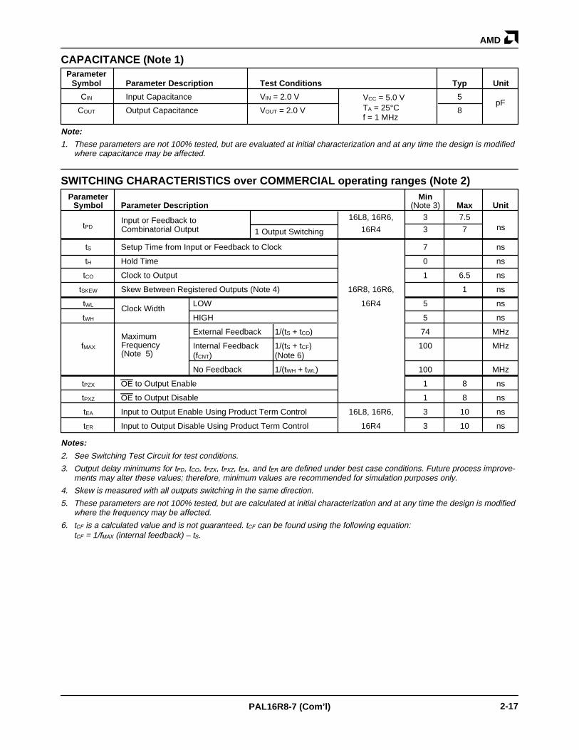
CAPACITANCE (Note 1)Parameter
Symbol Parameter Description Test Conditions Typ Unit
CIN Input Capacitance VIN = 2.0 V 5
COUT Output Capacitance VOUT = 2.0 V 8
VCC = 5.0 VTA = 25°Cf = 1 MHz
pF
Note:
1. These parameters are not 100% tested, but are evaluated at initial characterization and at any time the design is modified where capacitance may be affected.
SWITCHING CHARACTERISTICS over COMMERCIAL operating ranges (Note 2)Parameter Min
Symbol Parameter Description (Note 3) Max Unit16L8, 16R6, 3 7.5
16R4 3 7
tS Setup Time from Input or Feedback to Clock 7 ns
tH Hold Time 0 ns
tCO Clock to Output 1 6.5 ns
tSKEW Skew Between Registered Outputs (Note 4) 16R8, 16R6, 1 ns
tWL LOW 16R4 5 ns
tWH HIGH 5 ns
External Feedback 1/(tS + tCO) 74 MHz
fMAX Internal Feedback 1/(tS + tCF) 100 MHz(fCNT) (Note 6)
No Feedback 1/(tWH + tWL) 100 MHz
tPZX OE to Output Enable 1 8 ns
tPXZ OE to Output Disable 1 8 ns
tEA Input to Output Enable Using Product Term Control 16L8, 16R6, 3 10 ns
tER Input to Output Disable Using Product Term Control 16R4 3 10 ns
ns
MaximumFrequency(Note 5)
Clock Width
tPDInput or Feedback toCombinatorial Output 1 Output Switching
Notes:
2. See Switching Test Circuit for test conditions.
3. Output delay minimums for tPD, tCO, tPZX, tPXZ, tEA, and tER are defined under best case conditions. Future process improve-ments may alter these values; therefore, minimum values are recommended for simulation purposes only.
4. Skew is measured with all outputs switching in the same direction.
5. These parameters are not 100% tested, but are calculated at initial characterization and at any time the design is modifiedwhere the frequency may be affected.
6. tCF is a calculated value and is not guaranteed. tCF can be found using the following equation: tCF = 1/fMAX (internal feedback) – tS.
AMD
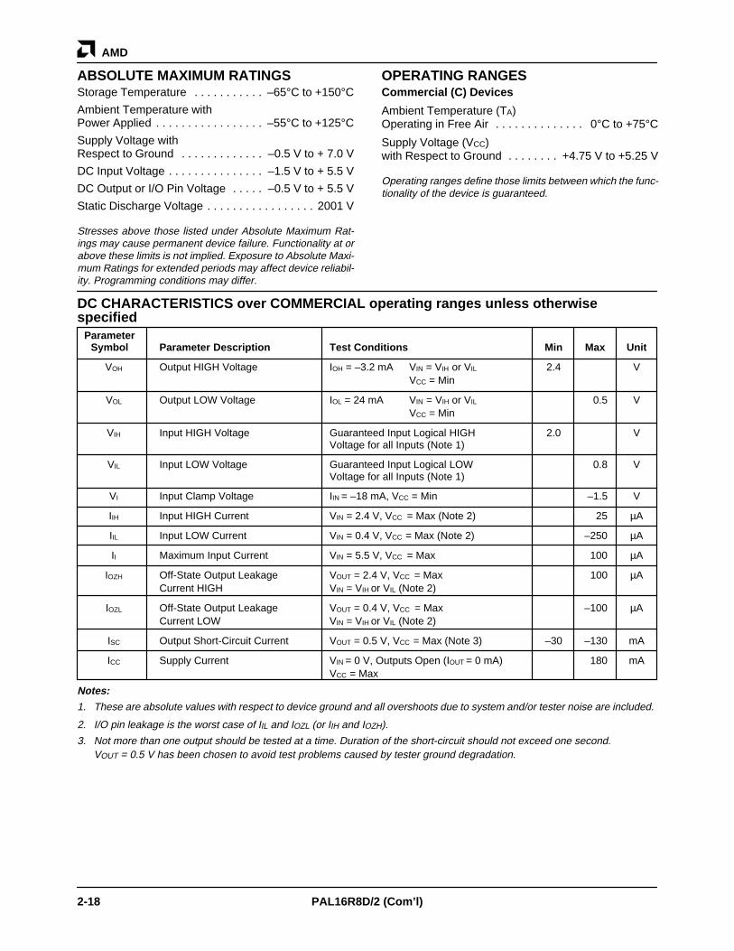
2-18 PAL16R8D/2 (Com’l)
ABSOLUTE MAXIMUM RATINGSStorage Temperature –65°C to +150°C. . . . . . . . . . .
Ambient Temperature withPower Applied –55°C to +125°C. . . . . . . . . . . . . . . . .
Supply Voltage with Respect to Ground –0.5 V to + 7.0 V. . . . . . . . . . . . .
DC Input Voltage –1.5 V to + 5.5 V. . . . . . . . . . . . . . .
DC Output or I/O Pin Voltage –0.5 V to + 5.5 V. . . . .
Static Discharge Voltage 2001 V. . . . . . . . . . . . . . . . .
Stresses above those listed under Absolute Maximum Rat-ings may cause permanent device failure. Functionality at orabove these limits is not implied. Exposure to Absolute Maxi-mum Ratings for extended periods may affect device reliabil-ity. Programming conditions may differ.
OPERATING RANGESCommercial (C) Devices
Ambient Temperature (TA)Operating in Free Air 0°C to +75°C. . . . . . . . . . . . . .
Supply Voltage (VCC)with Respect to Ground +4.75 V to +5.25 V. . . . . . . .
Operating ranges define those limits between which the func-tionality of the device is guaranteed.
DC CHARACTERISTICS over COMMERCIAL operating ranges unless otherwisespecified
ParameterSymbol Parameter Description Test Conditions Min Max Unit
VOH Output HIGH Voltage IOH = –3.2 mA VIN = VIH or VIL 2.4 VVCC = Min
VOL Output LOW Voltage IOL = 24 mA VIN = VIH or VIL 0.5 VVCC = Min
VIH Input HIGH Voltage Guaranteed Input Logical HIGH 2.0 VVoltage for all Inputs (Note 1)
VIL Input LOW Voltage Guaranteed Input Logical LOW 0.8 VVoltage for all Inputs (Note 1)
VI Input Clamp Voltage IIN = –18 mA, VCC = Min –1.5 V
IIH Input HIGH Current VIN = 2.4 V, VCC = Max (Note 2) 25 µA
IIL Input LOW Current VIN = 0.4 V, VCC = Max (Note 2) –250 µA
II Maximum Input Current VIN = 5.5 V, VCC = Max 100 µA
IOZH Off-State Output Leakage VOUT = 2.4 V, VCC = Max 100 µACurrent HIGH VIN = VIH or VIL (Note 2)
IOZL Off-State Output Leakage VOUT = 0.4 V, VCC = Max –100 µACurrent LOW VIN = VIH or VIL (Note 2)
ISC Output Short-Circuit Current VOUT = 0.5 V, VCC = Max (Note 3) –30 –130 mA
ICC Supply Current VIN = 0 V, Outputs Open (IOUT = 0 mA) 180 mAVCC = Max
Notes:
1. These are absolute values with respect to device ground and all overshoots due to system and/or tester noise are included.
2. I/O pin leakage is the worst case of IIL and IOZL (or IIH and IOZH).
3. Not more than one output should be tested at a time. Duration of the short-circuit should not exceed one second. VOUT = 0.5 V has been chosen to avoid test problems caused by tester ground degradation.
AMD
2-19PAL16R8D/2 (Com’l)
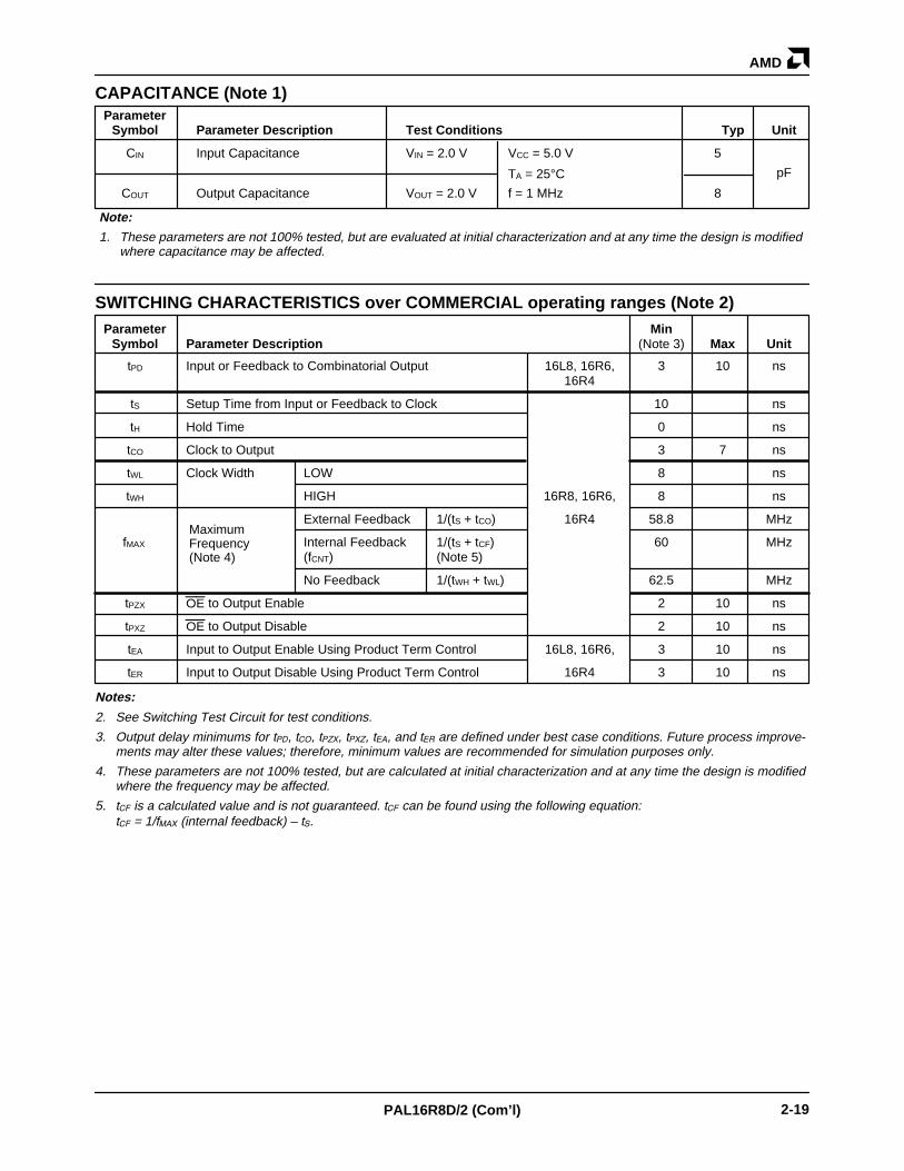
CAPACITANCE (Note 1)Parameter
Symbol Parameter Description Test Conditions Typ Unit
CIN Input Capacitance VIN = 2.0 V VCC = 5.0 V 5
COUT Output Capacitance VOUT = 2.0 V f = 1 MHz 8
Note:
1. These parameters are not 100% tested, but are evaluated at initial characterization and at any time the design is modified where capacitance may be affected.
TA = 25°C pF
SWITCHING CHARACTERISTICS over COMMERCIAL operating ranges (Note 2)Parameter Min
Symbol Parameter Description (Note 3) Max Unit
tPD Input or Feedback to Combinatorial Output 16L8, 16R6, 3 10 ns16R4
tS Setup Time from Input or Feedback to Clock 10 ns
tH Hold Time 0 ns
tCO Clock to Output 3 7 ns
tWL Clock Width LOW 8 ns
tWH HIGH 16R8, 16R6, 8 ns
External Feedback 1/(tS + tCO) 16R4 58.8 MHz
fMAX Internal Feedback 1/(tS + tCF) 60 MHz(fCNT) (Note 5)
No Feedback 1/(tWH + tWL) 62.5 MHz
tPZX OE to Output Enable 2 10 ns
tPXZ OE to Output Disable 2 10 ns
tEA Input to Output Enable Using Product Term Control 16L8, 16R6, 3 10 ns
tER Input to Output Disable Using Product Term Control 16R4 3 10 ns
MaximumFrequency(Note 4)
Notes:
2. See Switching Test Circuit for test conditions.
3. Output delay minimums for tPD, tCO, tPZX, tPXZ, tEA, and tER are defined under best case conditions. Future process improve-ments may alter these values; therefore, minimum values are recommended for simulation purposes only.
4. These parameters are not 100% tested, but are calculated at initial characterization and at any time the design is modifiedwhere the frequency may be affected.
5. tCF is a calculated value and is not guaranteed. tCF can be found using the following equation: tCF = 1/fMAX (internal feedback) – tS.
AMD
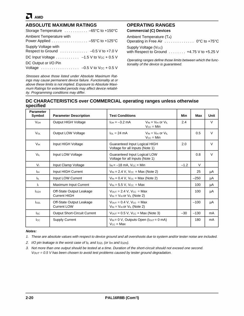
2-20 PAL16R8B (Com’l)
ABSOLUTE MAXIMUM RATINGSStorage Temperature –65°C to +150°C. . . . . . . . . . .
Ambient Temperature withPower Applied –55°C to +125°C. . . . . . . . . . . . . . . . .
Supply Voltage with Respect to Ground –0.5 V to +7.0 V. . . . . . . . . . . . .
DC Input Voltage –1.5 V to VCC + 0.5 V. . . . . . . . . . .
DC Output or I/O Pin Voltage –0.5 V to VCC + 0.5 V. . . . . . . . . . . . . . . . . .
Stresses above those listed under Absolute Maximum Rat-ings may cause permanent device failure. Functionality at orabove these limits is not implied. Exposure to Absolute Maxi-mum Ratings for extended periods may affect device reliabil-ity. Programming conditions may differ.
OPERATING RANGESCommercial (C) Devices
Ambient Temperature (TA)Operating in Free Air 0°C to +75°C. . . . . . . . . . . . . .
Supply Voltage (VCC)with Respect to Ground +4.75 V to +5.25 V. . . . . . . .
Operating ranges define those limits between which the func-tionality of the device is guaranteed.
DC CHARACTERISTICS over COMMERCIAL operating ranges unless otherwisespecified
ParameterSymbol Parameter Description Test Conditions Min Max Unit
VOH Output HIGH Voltage IOH = –3.2 mA VIN = VIH or VIL 2.4 VVCC = Min
VOL Output LOW Voltage IOL = 24 mA VIN = VIH or VIL 0.5 VVCC = Min
VIH Input HIGH Voltage Guaranteed Input Logical HIGH 2.0 VVoltage for all Inputs (Note 1)
VIL Input LOW Voltage Guaranteed Input Logical LOW 0.8 VVoltage for all Inputs (Note 1)
VI Input Clamp Voltage IIN = –18 mA, VCC = Min –1.2 V
IIH Input HIGH Current VIN = 2.4 V, VCC = Max (Note 2) 25 µA
IIL Input LOW Current VIN = 0.4 V, VCC = Max (Note 2) –250 µA
II Maximum Input Current VIN = 5.5 V, VCC = Max 100 µA
IOZH Off-State Output Leakage VOUT = 2.4 V, VCC = Max 100 µACurrent HIGH VIN = VIH or VIL (Note 2)
IOZL Off-State Output Leakage VOUT = 0.4 V, VCC = Max –100 µACurrent LOW VIN = VIH or VIL (Note 2)
ISC Output Short-Circuit Current VOUT = 0.5 V, VCC = Max (Note 3) –30 –130 mA
ICC Supply Current VIN = 0 V, Outputs Open (IOUT = 0 mA) 180 mAVCC = Max
Notes:
1. These are absolute values with respect to device ground and all overshoots due to system and/or tester noise are included.
2. I/O pin leakage is the worst case of IIL and IOZL (or IIH and IOZH).
3. Not more than one output should be tested at a time. Duration of the short-circuit should not exceed one second.VOUT = 0.5 V has been chosen to avoid test problems caused by tester ground degradation.
AMD
2-21PAL16R8B (Com’l)
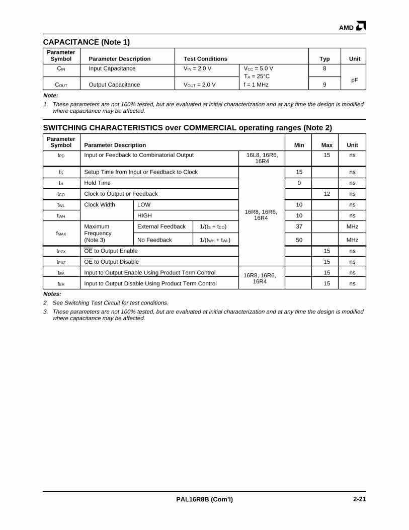
CAPACITANCE (Note 1)Parameter
Symbol Parameter Description Test Conditions Typ Unit
CIN Input Capacitance VIN = 2.0 V VCC = 5.0 V 8
COUT Output Capacitance VOUT = 2.0 V f = 1 MHz 9
TA = 25°CpF
Note:
1. These parameters are not 100% tested, but are evaluated at initial characterization and at any time the design is modifiedwhere capacitance may be affected.
SWITCHING CHARACTERISTICS over COMMERCIAL operating ranges (Note 2)Parameter
Symbol Parameter Description Min Max Unit
tPD Input or Feedback to Combinatorial Output 16L8, 16R6, 15 ns16R4
tS Setup Time from Input or Feedback to Clock 15 ns
tH Hold Time 0 ns
tCO Clock to Output or Feedback 12 ns
tWL Clock Width LOW 10 ns
tWH HIGH 10 ns
Maximum External Feedback 1/(tS + tCO) 37 MHzfMAX Frequency
(Note 3) No Feedback 1/(tWH + tWL) 50 MHz
tPZX OE to Output Enable 15 ns
tPXZ OE to Output Disable 15 ns
tEA Input to Output Enable Using Product Term Control 15 ns
tER Input to Output Disable Using Product Term Control 15 ns
16R8, 16R6,16R4
16R8, 16R6,16R4
Notes:
2. See Switching Test Circuit for test conditions.
3. These parameters are not 100% tested, but are evaluated at initial characterization and at any time the design is modifiedwhere capacitance may be affected.
AMD
2-22 PAL16R8B-2 (Com’l)
ABSOLUTE MAXIMUM RATINGSStorage Temperature –65°C to +150°C. . . . . . . . . . .
Ambient Temperature withPower Applied –55°C to +125°C. . . . . . . . . . . . . . . . .
Supply Voltage with Respect to Ground –0.5 V to +7.0 V. . . . . . . . . . . . .
DC Input Voltage –1.5 V to VCC + 0.5 V. . . . . . . . . . .
DC Output or I/O Pin Voltage –0.5 V to VCC + 0.5 V. . . . . . . . . . . . . . . . . .
Stresses above those listed under Absolute Maximum Rat-ings may cause permanent device failure. Functionality at orabove these limits is not implied. Exposure to Absolute Maxi-mum Ratings for extended periods may affect device reliabil-ity. Programming conditions may differ.
OPERATING RANGESCommercial (C) Devices
Ambient Temperature (TA)Operating in Free Air 0°C to +75°C. . . . . . . . . . . . . .
Supply Voltage (VCC)with Respect to Ground +4.75 V to +5.25 V. . . . . . . .
Operating ranges define those limits between which the func-tionality of the device is guaranteed.
DC CHARACTERISTICS over COMMERCIAL operating ranges unless otherwisespecified
ParameterSymbol Parameter Description Test Conditions Min Max Unit
VOH Output HIGH Voltage IOH = –3.2 mA VIN = VIH or VIL 2.4 VVCC = Min
VOL Output LOW Voltage IOL = 24 mA VIN = VIH or VIL 0.5 VVCC = Min
VIH Input HIGH Voltage Guaranteed Input Logical HIGH 2.0 VVoltage for all Inputs (Note 1)
VIL Input LOW Voltage Guaranteed Input Logical LOW 0.8 VVoltage for all Inputs (Note 1)
VI Input Clamp Voltage IIN = –18 mA, VCC = Min –1.2 V
IIH Input HIGH Current VIN = 2.7 V, VCC = Max (Note 2) 25 µA
IIL Input LOW Current VIN = 0.4 V, VCC = Max (Note 2) –100 µA
II Maximum Input Current VIN = 5.5 V, VCC = Max 100 µA
IOZH Off-State Output Leakage VOUT = 2.7 V, VCC = Max 100 µACurrent HIGH VIN = VIH or VIL (Note 2)
IOZL Off-State Output Leakage VOUT = 0.4 V, VCC = Max –100 µACurrent LOW VIN = VIH or VIL (Note 2)
ISC Output Short-Circuit Current VOUT = 0.5 V, VCC = Max (Note 3) –30 –130 mA
ICC Supply Current VIN = 0 V, Outputs Open (IOUT = 0 mA) 90 mAVCC = Max
Notes:
1. These are absolute values with respect to device ground and all overshoots due to system and/or tester noise are included.
2. I/O pin leakage is the worst case of IIL and IOZL (or IIH and IOZH).
3. Not more than one output should be tested at a time. Duration of the short-circuit should not exceed one second. VOUT = 0.5 Vhas been chosen to avoid test problems caused by tester ground degradation.
AMD
2-23PAL16R8B-2 (Com’l)
CAPACITANCE (Note 1)Parameter
Symbol Parameter Description Test Conditions Typ Unit
CIN Input Capacitance VIN = 2.0 V VCC = 5.0 V 7
COUT Output Capacitance VOUT = 2.0 V f = 1 MHz 7TA = 25°C pF
Note:
1. These parameters are not 100% tested, but are evaluated at initial characterization and at any time the design is modifiedwhere capacitance may be affected.
SWITCHING CHARACTERISTICS over COMMERCIAL operating ranges (Note 2)Parameter
Symbol Parameter Description Min Max Unit
tPD Input or Feedback to Combinatorial Output 16L8, 16R6, 25 ns16R4
tS Setup Time from Input or Feedback to Clock 25 ns
tH Hold Time 0 ns
tCO Clock to Output 15 ns
tWL Clock Width LOW 15 ns
tWH HIGH 15 ns
External Feedback 1/(tS + tCO) 25 MHz
fMAX Internal Feedback 1/(tS + tCF) 28.5 MHz(fCNT) (Note 5)
No Feedback 1/(tWH + tWL) 33 MHz
tPZX OE to Output Enable 20 ns
tPXZ OE to Output Disable 20 ns
tEA Input to Output Enable Using Product Term Control 25 ns
tER Input to Output Disable Using Product Term Control 25 ns
MaximumFrequency(Note 4)
16R8, 16R6, 16R4
16R8, 16R6, 16R4
Notes:
2. See Switching Test Circuit for test conditions.
3. Calculated from measured fMAX internal.
4. These parameters are not 100% tested, but are calculated at initial characterization and at any time the design is modifiedwhere frequency may be affected.
5. tCF is a calculated value and is not guaranteed. tCF can be found using the following equation: tCF = 1/fMAX (internal feedback) – tS.

AMD
2-24 PAL16R8A (Com’l)
ABSOLUTE MAXIMUM RATINGSStorage Temperature –65°C to +150°C. . . . . . . . . . .
Ambient Temperature withPower Applied –55°C to +125°C. . . . . . . . . . . . . . . . .
Supply Voltage with Respect to Ground –0.5 V to + 7.0 V. . . . . . . . . . . . .
DC Input Voltage –1.5 V to VCC + 0.5 V. . . . . . . . . . .
DC Output or I/O Pin Voltage –0.5 V to VCC + 0.5 V. . . . . . . . . . . . . . . . . .
Stresses above those listed under Absolute Maximum Rat-ings may cause permanent device failure. Functionality at orabove these limits is not implied. Exposure to Absolute Maxi-mum Ratings for extended periods may affect device reliabil-ity. Programming conditions may differ.
OPERATING RANGESCommercial (C) Devices
Ambient Temperature (TA)Operating in Free Air 0°C to +75°C. . . . . . . . . . . . . .
Supply Voltage (VCC)with Respect to Ground +4.75 V to +5.25 V. . . . . . . .
Operating ranges define those limits between which the func-tionality of the device is guaranteed.
DC CHARACTERISTICS over COMMERCIAL operating ranges unless otherwisespecified
ParameterSymbol Parameter Description Test Conditions Min Max Unit
VOH Output HIGH Voltage IOH = –3.2 mA VIN = VIH or VIL 2.4 VVCC = Min
VOL Output LOW Voltage IOL = 24 mA VIN = VIH or VIL 0.5 VVCC = Min
VIH Input HIGH Voltage Guaranteed Input Logical HIGH 2.0 VVoltage for all Inputs (Note 1)
VIL Input LOW Voltage Guaranteed Input Logical LOW 0.8 VVoltage for all Inputs (Note 1)
VI Input Clamp Voltage IIN = –18 mA, VCC = Min –1.2 V
IIH Input HIGH Current VIN = 2.7 V, VCC = Max (Note 2) 25 µA
IIL Input LOW Current VIN = 0.4 V, VCC = Max (Note 2) –250 µA
II Maximum Input Current VIN = 5.5 V, VCC = Max 100 µA
IOZH Off-State Output Leakage VOUT = 2.7 V, VCC = Max 100 µACurrent HIGH VIN = VIH or VIL (Note 2)
IOZL Off-State Output Leakage VOUT = 0.4 V, VCC = Max –100 µACurrent LOW VIN = VIH or VIL (Note 2)
ISC Output Short-Circuit Current VOUT = 0.5 V, VCC = Max (Note 3) –30 –130 mA
16L8 VIN = 0 V, Outputs Open (IOUT = 0 mA) 155 mA16R8/6/4 VCC = Max 180
ICC Supply Current
Notes:
1. These are absolute values with respect to device ground and all overshoots due to system and/or tester noise are included.
2. I/O pin leakage is the worst case of IIL and IOZL (or IIH and IOZH).
3. Not more than one output should be tested at a time. Duration of the short-circuit should not exceed one second. VCC = 0.5 Vhas been chosen to avoid test problems caused by tester ground degradation.
AMD
2-25PAL16R8A (Com’l)
CAPACITANCE (Note 1)Parameter
Symbol Parameter Description Test Conditions Typ Unit
CIN Input Capacitance VIN = 2.0 V VCC = 5.0 V 7
COUT Output Capacitance VOUT = 2.0 V f = 1 MHz 7TA = 25°C pF
Note:
1. These parameters are not 100% tested, but are evaluated at initial characterization and at any time the design is modified where capacitance may be affected.
SWITCHING CHARACTERISTICS over COMMERCIAL operating ranges (Note 2)Parameter
Symbol Parameter Description Min Max Unit
tPD Input or Feedback to Combinatorial Output 16L8, 16R6, 25 ns16R4
tS Setup Time from Input or Feedback to Clock 25 ns
tH Hold Time 0 ns
tCO Clock to Output 15 ns
tWL Clock Width LOW 15 ns
tWH HIGH 15 ns
External Feedback 1/(tS + tCO) 25 MHz
fMAX Internal Feedback 1/(tS + tCF) 28.5 MHz(fCNT) (Note 5)
No Feedback 1/(tWH + tWL) 33 MHz
tPZX OE to Output Enable 20 ns
tPXZ OE to Output Disable 20 ns
tEA Input to Output Enable Using Product Term Control 25 ns
tER Input to Output Disable Using Product Term Control 25 ns
MaximumFrequency(Note 4)
16R8, 16R6,16R4
16R8, 16R6,16R4
Notes:
2. See Switching Test Circuit for test conditions.
3. Calculated from measured fMAX internal.
4. These parameters are not 100% tested, but are calculated at initial characterization and at any time the design is modifiedwhere frequency may be affected.
5. tCF is a calculated value and is not guaranteed. tCF can be found using the following equation: tCF = 1/fMAX (internal feedback) – tS.
AMD
2-26 PAL16R8B-4 (Com’l)
ABSOLUTE MAXIMUM RATINGSStorage Temperature –65°C to +150°C. . . . . . . . . . .
Ambient Temperature withPower Applied –55°C to +125°C. . . . . . . . . . . . . . . . .
Supply Voltage with Respect to Ground –0.5 V to +7.0 V. . . . . . . . . . . . .
DC Input Voltage –1.5 V to +5.5 V. . . . . . . . . . . . . . .
DC Output or I/O Pin Voltage 5.5 V. . . . . . . . . . . . . .
Stresses above those listed under Absolute Maximum Rat-ings may cause permanent device failure. Functionality at orabove these limits is not implied. Exposure to Absolute Maxi-mum Ratings for extended periods may affect device reliabil-ity. Programming conditions may differ.
OPERATING RANGESCommercial (C) Devices
Ambient Temperature (TA)Operating in Free Air 0°C to +75°C. . . . . . . . . . . . . .
Supply Voltage (VCC)with Respect to Ground +4.75 V to +5.25 V. . . . . . . .
Operating ranges define those limits between which the func-tionality of the device is guaranteed.
DC CHARACTERISTICS over COMMERCIAL operating ranges unless otherwisespecified
ParameterSymbol Parameter Description Test Conditions Min Max Unit
VOH Output HIGH Voltage IOH = –1 mA VIN = VIH or VIL 2.4 VVCC = Min
VOL Output LOW Voltage IOL = 8 mA VIN = VIH or VIL 0.5 VVCC = Min
VIH Input HIGH Voltage Guaranteed Input Logical HIGH 2.0 VVoltage for all Inputs (Note 1)
VIL Input LOW Voltage Guaranteed Input Logical LOW 0.8 VVoltage for all Inputs (Note 1)
VI Input Clamp Voltage IIN = –18 mA, VCC = Min –1.5 V
IIH Input HIGH Current VIN = 2.4 V, VCC = Max (Note 2) 25 µA
IIL Input LOW Current VIN = 0.4 V, VCC = Max (Note 2) –250 µA
II Maximum Input Current VIN = 5.5 V, VCC = Max 100 µA
IOZH Off-State Output Leakage VOUT = 2.4 V, VCC = Max 100 µACurrent HIGH VIN = VIH or VIL (Note 2)
IOZL Off-State Output Leakage VOUT = 0.4 V, VCC = Max –100 µACurrent LOW VIN = VIH or VIL (Note 2)
ISC Output Short-Circuit Current VOUT = 0.5 V, VCC = Max (Note 3) –30 –250 mA
ICC Supply Current VIN = 0 V, Outputs Open (IOUT = 0 mA) 55 mAVCC = Max
Notes:
1. These are absolute values with respect to device ground and all overshoots due to system and/or tester noise are included.
2. I/O pin leakage is the worst case of IIL and IOZL (or IIH and IOZH).
3. Not more than one output should be tested at a time. Duration of the short-circuit should not exceed one second.VOUT = 0.5 V as been chosen to avoid test problems caused by tester ground degradation.
AMD
2-27PAL16R8B-4 (Com’l)
SWITCHING CHARACTERISTICS over COMMERCIAL operating ranges (Note 1)Parameter
Symbol Parameter Description Min Max Unit
tPD Input or Feedback to Combinatorial Output 16L8, 16R6, 35 ns16R4
tS Setup Time from Input or Feedback to Clock 35 ns
tH Hold Time 0 ns
tCO Clock to Output or Feedback 16R8, 16R6, 25 ns
tWL Clock Width LOW 16R4 25 ns
tWH HIGH 25 ns
Maximum External Feedback 1/(tS + tCO) 16 MHzfMAX Frequency
(Note 2) No Feedback 1/(tWH + tWL) 20 MHz
tPZX OE to Output Enable 25 ns
tPXZ OE to Output Disable 25 ns
tEA Input to Output Enable Using Product Term Control 16L8, 16R6, 35 ns
tER Input to Output Disable Using Product Term Control 16R4 35 ns
Notes:
1. See Switching Test Circuit for test conditions.
2. These parameters are not 100% tested, but are calculated at initial characterization and at any time the design is modifiedwhere frequency may be affected.
AMD
2-28 PAL16R8 Family
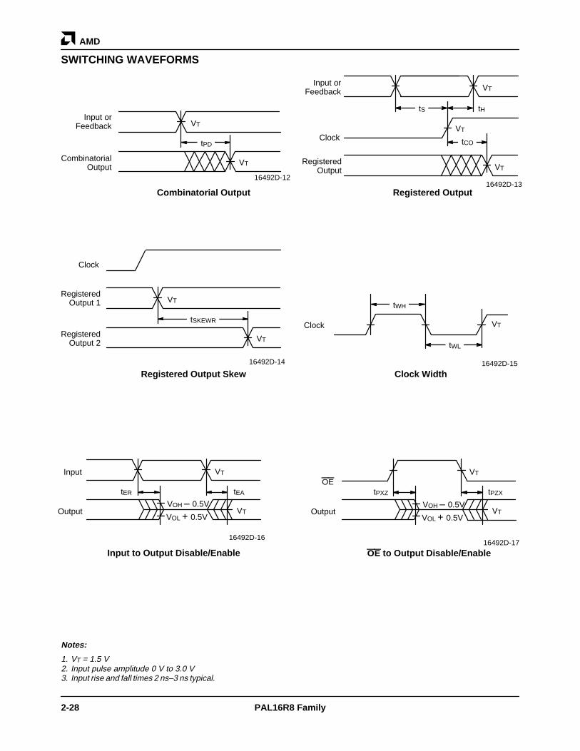
SWITCHING WAVEFORMS
tPD
Input orFeedback
CombinatorialOutput
VT
VT
Combinatorial Output
VTInput or
Feedback
RegisteredOutput
Registered Output
tS
tCO
VT
tH
VTClock
VT
tWH
Clock
Clock Width
tWL
Clock
tSKEWR
VT
VT
RegisteredOutput 1
RegisteredOutput 2
Registered Output Skew
Notes:
1. VT = 1.5 V2. Input pulse amplitude 0 V to 3.0 V3. Input rise and fall times 2 ns–3 ns typical.
VT
VT
Input
Output
Input to Output Disable/Enable
tER tEA
VT
VT
OE
Output
OE to Output Disable/Enable
tPZXtPXZ
VOH – 0.5V
VOL + 0.5V
VOH – 0.5V
VOL + 0.5V
16492D-1216492D-13
16492D-14 16492D-15
16492D-1616492D-17
AMD
2-29PAL16R8 Family
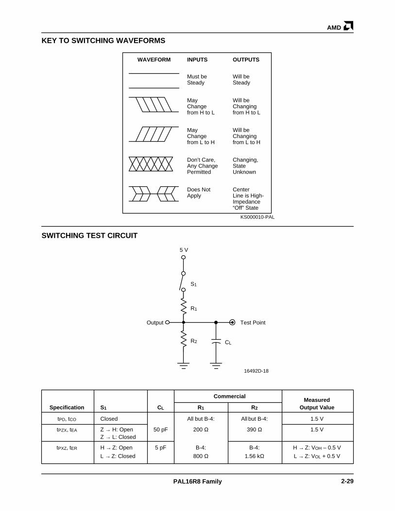
KEY TO SWITCHING WAVEFORMS
KS000010-PAL
Must beSteady
MayChangefrom H to L
MayChangefrom L to H
Does Not Apply
Don’t Care,Any ChangePermitted
Will beSteady
Will beChangingfrom H to L
Will be Changing from L to H
Changing,StateUnknown
Center Line is High-Impedance“Off” State
WAVEFORM INPUTS OUTPUTS
SWITCHING TEST CIRCUIT
CL
Output
R1
R2
S1
Test Point
5 V
16492D-18
MeasuredSpecification S 1 CL R1 R2 Output Value
tPD, tCO Closed All but B-4: All but B-4: 1.5 V
tPZX, tEA Z → H: Open 50 pF 200 Ω 390 Ω 1.5 VZ → L: Closed
tPXZ, tER H → Z: Open 5 pF B-4: B-4: H → Z: VOH – 0.5 V
L → Z: Closed 800 Ω 1.56 kΩ L → Z: VOL + 0.5 V
Commercial
AMD
2-30 PAL16R8-5
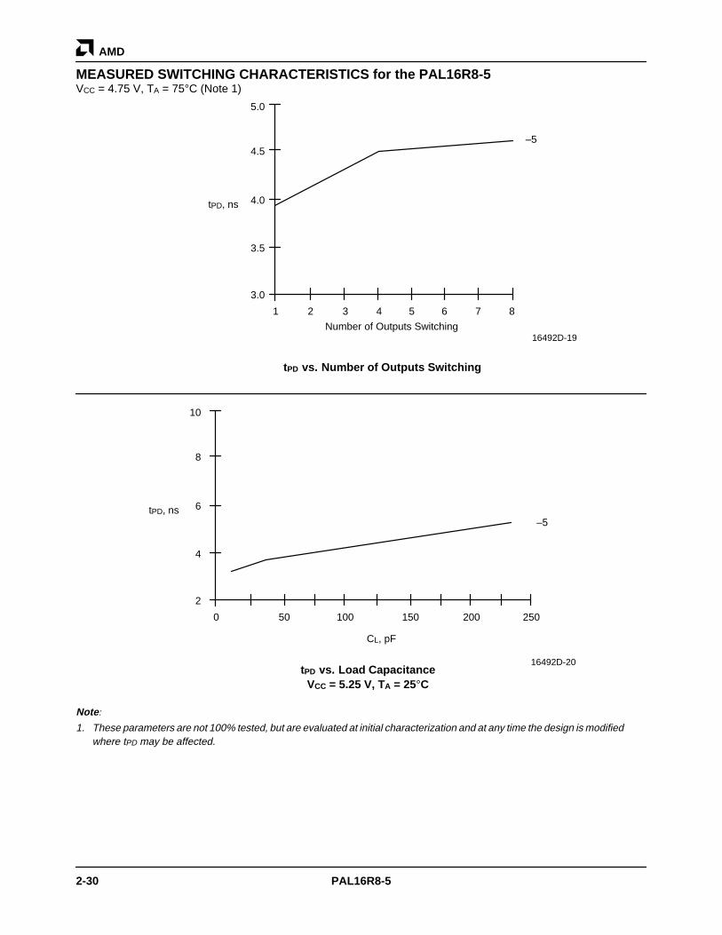
MEASURED SWITCHING CHARACTERISTICS for the PAL16R8-5VCC = 4.75 V, TA = 75°C (Note 1)
tPD vs. Number of Outputs Switching
tPD vs. Load CapacitanceVCC = 5.25 V, TA = 25°C
Note :
1. These parameters are not 100% tested, but are evaluated at initial characterization and at any time the design is modifiedwhere tPD may be affected.
5.0
4.5
4.0
3.5
3.0
1 2 3 4 5 6 7 8
tPD, ns
Number of Outputs Switching
10
8
6
4
2
0 50 100
tPD, ns
150 200 250
–5
CL, pF
–5
16492D-19
16492D-20
AMD
2-31PAL16R8-5
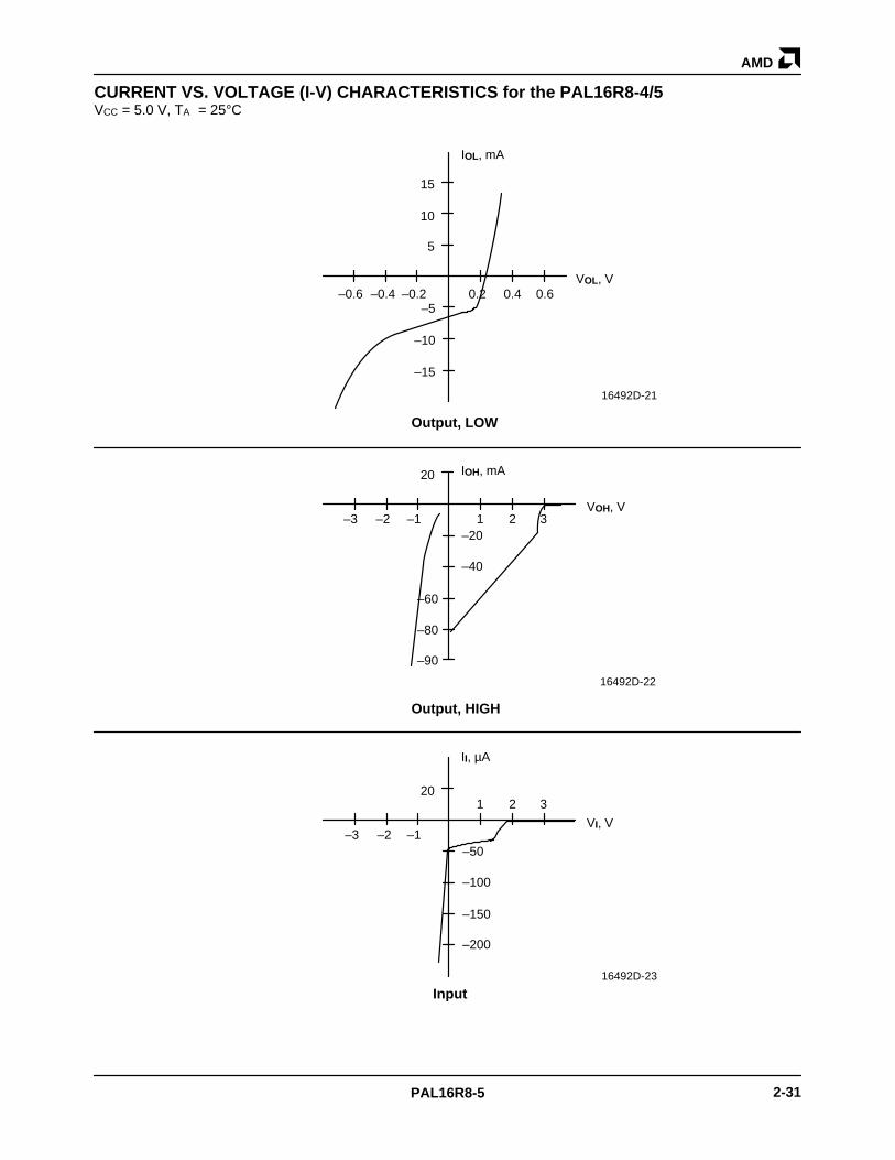
CURRENT VS. VOLTAGE (I-V) CHARACTERISTICS for the PAL16R8-4/5VCC = 5.0 V, TA = 25°C
15
10
Output, LOW
IOL, mA
5
–5
–10
–15
–0.6 –0.4 –0.2 0.2 0.4 0.6VOL, V
20
–40
–60
–80
–3 –2 –1 1 2 3
Output, HIGH
IOH, mA
VOH, V
–20
Input
II, µA
VI, V
20
–100
–150
–200
–3 –2 –1
1 2 3
–50
–90
16492D-21
16492D-22
16492D-23
AMD
2-32 PAL16R8-7
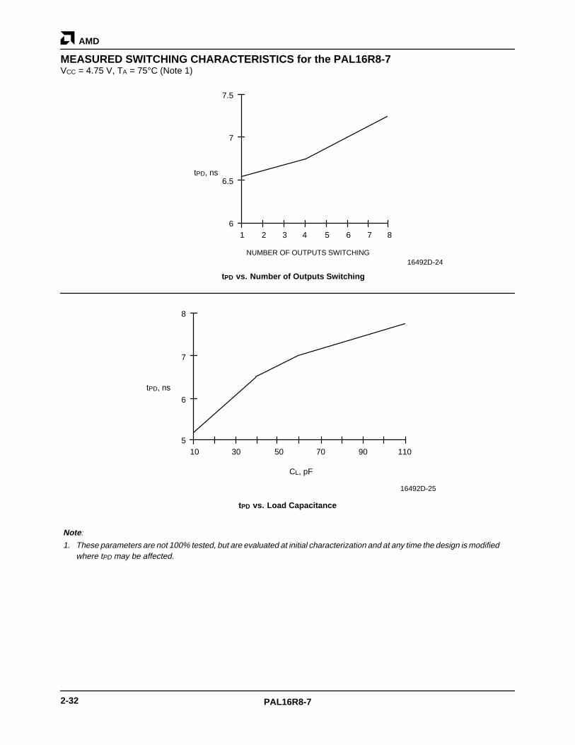
MEASURED SWITCHING CHARACTERISTICS for the PAL16R8-7VCC = 4.75 V, TA = 75°C (Note 1)
7.5
7
6.5
61 2 3 4 5 6 7 8
NUMBER OF OUTPUTS SWITCHING
tPD vs. Number of Outputs Switching
8
7
6
510 30 50 70
CL, pF
tPD, ns
tPD, ns
90 110
tPD vs. Load Capacitance
Note :
1. These parameters are not 100% tested, but are evaluated at initial characterization and at any time the design is modifiedwhere tPD may be affected.
16492D-24
16492D-25
AMD
2-33PAL16R8-7
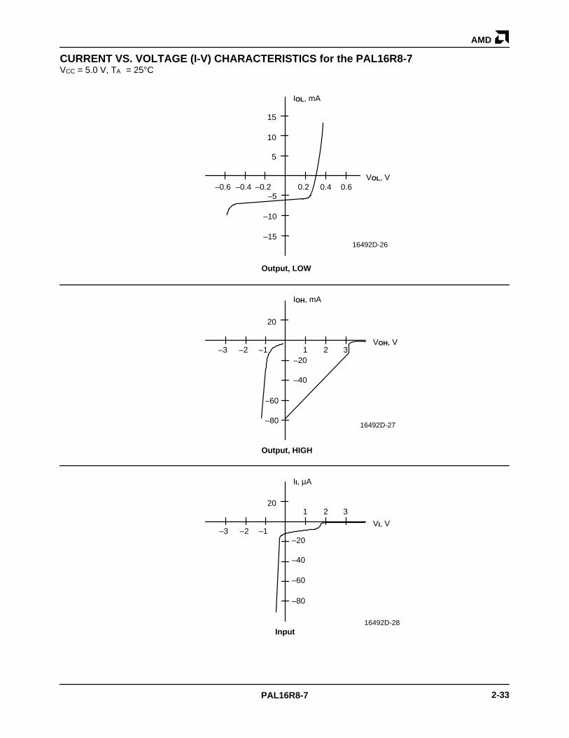
CURRENT VS. VOLTAGE (I-V) CHARACTERISTICS for the PAL16R8-7VCC = 5.0 V, TA = 25°C
15
10
Output, LOW
IOL, mA
5
–5
–10
–15
–0.6 –0.4 –0.2 0.2 0.4 0.6VOL, V
20
–40
–60
–80
–3 –2 –1 1 2 3
Output, HIGH
IOH, mA
VOH, V
–20
Input
II, µA
VI, V
20
–40
–60
–80
–3 –2 –1
1 2 3
–20
16492D-26
16492D-27
16492D-28
AMD
2-34 PAL16R8-5
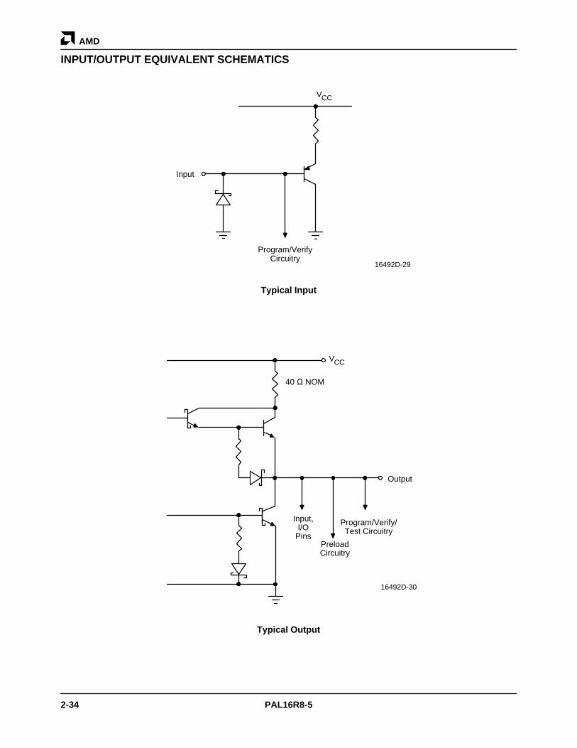
INPUT/OUTPUT EQUIVALENT SCHEMATICS
Typical Input
Input
CCV
Output
Typical Output
40 Ω NOM
Input,I/O
PinsPreloadCircuitry
Program/Verify/Test Circuitry
Program/VerifyCircuitry
CCV
16492D-29
16492D-30
AMD
2-35PAL16R8 Family
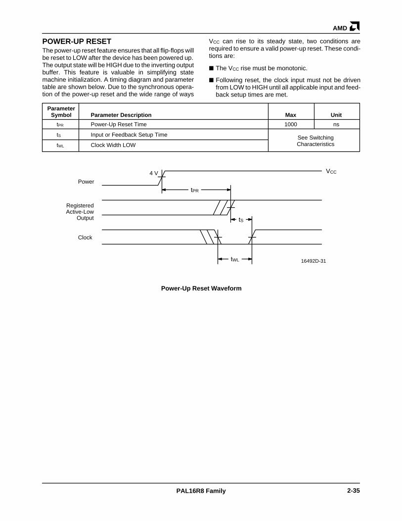
POWER-UP RESETThe power-up reset feature ensures that all flip-flops willbe reset to LOW after the device has been powered up.The output state will be HIGH due to the inverting outputbuffer. This feature is valuable in simplifying statemachine initialization. A timing diagram and parametertable are shown below. Due to the synchronous opera-tion of the power-up reset and the wide range of ways
VCC can rise to its steady state, two conditions arerequired to ensure a valid power-up reset. These condi-tions are:
The VCC rise must be monotonic.
Following reset, the clock input must not be drivenfrom LOW to HIGH until all applicable input and feed-back setup times are met.
ParameterSymbol Parameter Description Max Unit
tPR Power-Up Reset Time 1000 ns
tS Input or Feedback Setup Time
tWL Clock Width LOW
tPR
tWL
tS
4 V VCC
Power
RegisteredActive-Low
Output
Clock
16492D-31
See SwitchingCharacteristics
Power-Up Reset Waveform