Embed Size (px)
Citation preview
PAN1740 Bluetooth Low Energy Module
Product Specification
Rev. 1.7
Wireless Modules
PAN1740 Bluetooth Module
Product Specification Rev. 1.7 Page 2
Overview
The PAN1740 is a short-range BLE single mode
module used for the implementation of Bluetooth
functionality into various electronic devices.
Features
• Pre-programmed BT/MAC address
• Includes 16 MHz and 32 768 kHz crystal calibrated up to 1 ppm
• Single-mode Bluetooth Smart System-on-Chip
• Programmable ARM CORTEX M0 CPU
• Autonomous BTLE stand-alone operation
• Bluetooth v4.1 (LE) embedded GATT profile – Low Energy single mode
• Small 9.0 mm x 9.5 mm x 1.8 mm SMD package with antenna
• Less than a few µA in low power modes
• Integrated shielding to resist EMI
• No external components needed
Characteristics
• Peak power consumption 4.9 mA Rx and Tx
• Link budget 93 dBm (Rx sensitivity -93, Tx 0 dBm)
• Operating temperature range -40 °C to +85 °C
Block Diagram
Chip
Antenna
Dialog
DA14580
Slow Clock
32 KHz
UART/SPI/I2C
GPIOs
Quad Decoder
ADC/Wake-up
Reset
Vcc 3.3 V
PAN1740
Bluetooth 4.1 Module
Crystal
16 MHz
DC-DC
Conversion
PAN1740 Bluetooth Module
Product Specification Rev. 1.7 Page 3
By purchase of any of the products described in this document the customer accepts the document's
validity and declares their agreement and understanding of its contents and recommendations. Panasonic
reserves the right to make changes as required at any time without notification. Please consult the most
recently issued Product Specification before initiating or completing a design.
© Panasonic Industrial Devices Europe GmbH 2017.
This specification sheet is copyrighted. Reproduction of this document is permissible only if reproduction is
without alteration and is accompanied by all associated warranties, conditions, limitations, and notices. Do
not disclose it to a third party.
All rights reserved.
This Product Specification does not lodge the claim to be complete and free of mistakes.
Engineering Samples (ES)
If Engineering Samples are delivered to the customer, these samples have the status “Engineering
Samples”. This means that the design of this product is not yet concluded. Engineering Samples may be
partially or fully functional, and they may differ from the published Product Specification.
Engineering Samples are not qualified and they are not to be used for reliability testing or series
production.
Disclaimer
The customer acknowledges that samples may deviate from the Product Specification and may bear
defects due to their status of development and the lack of qualification mentioned above.
Panasonic rejects any liability or product warranty for Engineering Samples. In particular, Panasonic
disclaims liability for damages caused by:
The use of the Engineering Sample other than for evaluation purposes, particularly the installation
or integration in another product to be sold by the customer,
Deviation or lapse in function of the Engineering Sample,
Improper use of the Engineering Sample.
Panasonic Industrial Devices Europe GmbH disclaims any liability for consequential and incidental
damages. In case of any queries regarding the Engineering Samples, please contact your local sales
partner or the related product manager.
PAN1740 Bluetooth Module
Product Specification Rev. 1.7 Page 4
Table of Contents
1 About This Document ......................................................................................................................... 6
1.1 Purpose and Audience .............................................................................................................. 6
1.2 Revision History ......................................................................................................................... 6
1.3 Use of Symbols ......................................................................................................................... 6
1.4 Related Documents ................................................................................................................... 6
2 Overview .............................................................................................................................................. 7
2.1 Block Diagram ........................................................................................................................... 8
2.2 Bluetooth IC ............................................................................................................................... 9
2.3 System Overview ....................................................................................................................... 9
2.4 Pin Configuration ..................................................................................................................... 13
2.5 Interfaces ................................................................................................................................. 15
3 Detailed Description ......................................................................................................................... 19
3.1 Dimensions .............................................................................................................................. 19
3.2 Footprint .................................................................................................................................. 20
3.3 Packaging ................................................................................................................................ 21
3.4 Case Marking .......................................................................................................................... 24
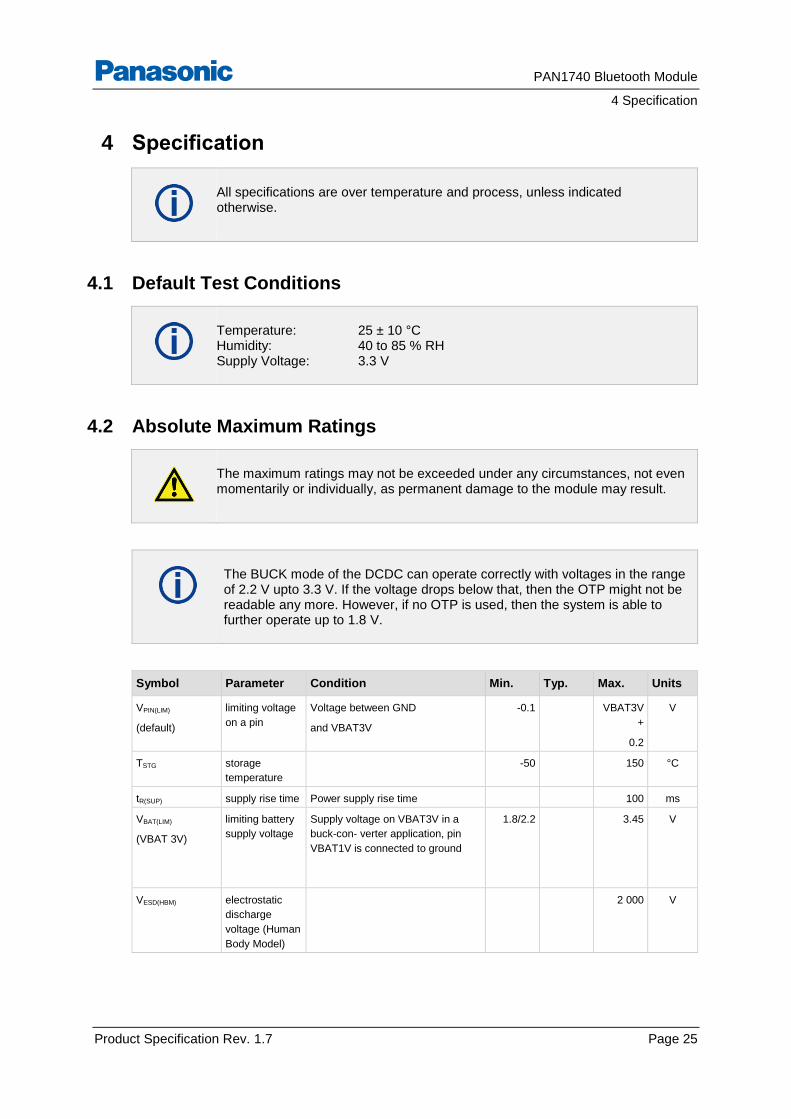
4 Specification ..................................................................................................................................... 25
4.1 Default Test Conditions ........................................................................................................... 25
4.2 Absolute Maximum Ratings ..................................................................................................... 25
4.3 Recommended Operating Conditions ...................................................................................... 26
4.4 DC Characteristics ................................................................................................................... 26
4.5 MHz Crystal Oscillator: Timing Characteristics ........................................................................ 27
4.6 32 kHz Crystal Oscillator: Timing Characteristics .................................................................... 27
4.7 DC-DC Converter: DC Characteristics ..................................................................................... 27
4.8 Reliability Tests ....................................................................................................................... 28
4.9 Recommended Soldering Profile ............................................................................................. 29
5 Cautions ............................................................................................................................................ 30
5.1 Design Notes ........................................................................................................................... 30
5.2 Installation Notes ..................................................................................................................... 30
5.3 Usage Condition Notes ............................................................................................................ 31
5.4 Storage Notes .......................................................................................................................... 31
5.5 Safety Cautions ....................................................................................................................... 31
5.6 Other Cautions ........................................................................................................................ 32
5.7 Life Support Policy ................................................................................................................... 32
6 Regulatory and Certification Information ....................................................................................... 33
6.1 Federal Communications Commission (FCC) for US .............................................................. 33
6.2 Industry Canada Certification .................................................................................................. 35
6.3 Japanese Radio Law Compliance ........................................................................................... 37
6.4 European Conformity According to RED (2014/53/EU) ........................................................... 38
6.5 Bluetooth ................................................................................................................................. 38
6.6 RoHS and REACH Declaration ............................................................................................... 38
PAN1740 Bluetooth Module
Product Specification Rev. 1.7 Page 5
7 Appendix ........................................................................................................................................... 39
7.1 Ordering Information ................................................................................................................ 39
7.2 Contact Details ........................................................................................................................ 40
PAN1740 Bluetooth Module
1 About This Document
Product Specification Rev. 1.7 Page 6
1 About This Document
1.1 Purpose and Audience
This Product Specification provides details on the functional, operational, and electrical
characteristics of the Panasonic PAN1740 module. It is intended for hardware design,
application, and Original Equipment Manufacturer (OEM) engineers. The product is referred to
as “the PAN1740” or “the module” within this document.
1.2 Revision History
Revision Date Modifications/Remarks
0.1 February 2014 1st preliminary version.
0.2 April 2014 Included Bluetooth 4.1 compliance.
0.3 June 2014 Formating Table 5. Updated Key Features.
1.0 October 2014 Final Specification incl. DoC.
1.1 December 2014 Changed tolerances in chapter 11 Module Dimension.
1.2 April 2015 Added nntrinsic safety values.
1.3 January 2016 Editorial changes.
1.4 October 2016 Updated EU regulatory chapter. Changed VCC to VBAT3V.
1.5 June 2017 Updated EU regulatory chapter to RED.
1.6 June 2017 New layout and document structure
1.7 November 2017 Added MIC ID for Japanese Radio Law
1.3 Use of Symbols
Symbol Description
Note
Indicates important information for the proper use of the product.
Non-observance can lead to errors.
Attention
Indicates important notes that, if not observed, can put the product’s functionality
at risk.
[chapter number]
[chapter title]
Cross reference
Indicates cross references within the document.
Example:
Description of the symbols used in this document 1.3 Use of Symbols.
1.4 Related Documents
Please refer to the Panasonic website for related documents 7.2.2 Product Information.
PAN1740 Bluetooth Module
2 Overview
Product Specification Rev. 1.7 Page 7
2 Overview
The PAN1740 is a short-range BLE single mode module used for the implementation of
Bluetooth functionality into various electronic devices. The PAN1740 is fully-compliant with the
Bluetooth V4.1 standard. It includes dedicated hardware for Link Layer implementation of
Bluetooth®Smart and interface controllers for enhanced connectivity capabilities.
Please refer to the Panasonic website for related documents 7.2.2 Product Information.
Further information on the variants and versions 7.1 Ordering Information.
PAN1740 Bluetooth Module
2 Overview
Product Specification Rev. 1.7 Page 8
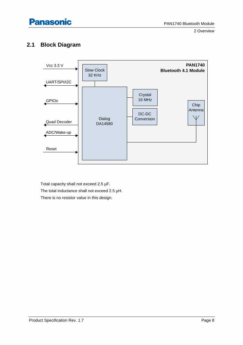
2.1 Block Diagram
Total capacity shall not exceed 2.5 µF.
The total inductance shall not exceed 2.5 µH.
There is no resistor value in this design.
Chip
Antenna
Dialog
DA14580
Slow Clock
32 KHz
UART/SPI/I2C
GPIOs
Quad Decoder
ADC/Wake-up
Reset
Vcc 3.3 V
PAN1740
Bluetooth 4.1 Module
Crystal
16 MHz
DC-DC
Conversion
PAN1740 Bluetooth Module
2 Overview
Product Specification Rev. 1.7 Page 9
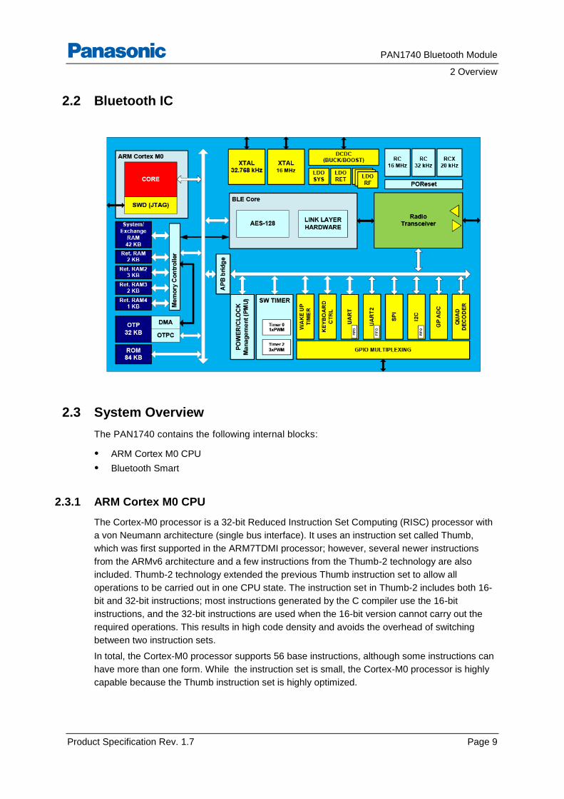
2.2 Bluetooth IC
2.3 System Overview
The PAN1740 contains the following internal blocks:
• ARM Cortex M0 CPU
• Bluetooth Smart
2.3.1 ARM Cortex M0 CPU
The Cortex-M0 processor is a 32-bit Reduced Instruction Set Computing (RISC) processor with
a von Neumann architecture (single bus interface). It uses an instruction set called Thumb,
which was first supported in the ARM7TDMI processor; however, several newer instructions
from the ARMv6 architecture and a few instructions from the Thumb-2 technology are also
included. Thumb-2 technology extended the previous Thumb instruction set to allow all
operations to be carried out in one CPU state. The instruction set in Thumb-2 includes both 16-
bit and 32-bit instructions; most instructions generated by the C compiler use the 16-bit
instructions, and the 32-bit instructions are used when the 16-bit version cannot carry out the
required operations. This results in high code density and avoids the overhead of switching
between two instruction sets.
In total, the Cortex-M0 processor supports 56 base instructions, although some instructions can
have more than one form. While the instruction set is small, the Cortex-M0 processor is highly
capable because the Thumb instruction set is highly optimized.
PAN1740 Bluetooth Module
2 Overview
Product Specification Rev. 1.7 Page 10
2.3.2 Bluetooth Smart
BLE Core
The BLE (Bluetooth Low Energy) core is a qualified Bluetooth v4.1 baseband controller
compatible with Bluetooth Smart specification and it is in charge of packet encoding- decoding
and frame scheduling.
• Bluetooth Smart Specifications compliant according to the Specification of the Bluetooth System, v4.1, Bluetooth SIG.
• All device classes are supported -- Broadcast, Central, Observer, Peripheral)
• All packet types (Advertising / Data / Control)
• Encryption (AES / CCM)
• Bit stream processing (CRC, Whitening)
• FDMA / TDMA / events formatting and synchronization
• Frequency Hopping calculation
• Operating clock with internal 16 MHz
• Low power modes with internal 32.678 kHz
• Supports power down of the baseband during the protocol’s idle periods.
• Advanced High performance Bus (AHB) Slave interface for register file access.
• AHB Slave interface for Exchange Memory access of CPU via BLE core.
• AHB Master interface for direct access of BLE core to Exchange Memory space
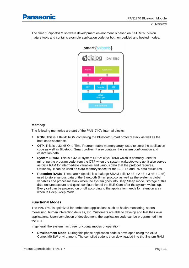
Smart Snippets
The PAN1740 is available together with Dialog’s SmartSnippetsTM Bluetooth Software platform
which includes a qualified Bluetooth Smart single-mode stack on chip.
Numerous Bluetooth Smart profiles for consumer wellness, sport, fitness, security and proximity
applications are supplied as standard, while additional customer profiles can be developed and
added as needed.
PAN1740 Bluetooth Module
2 Overview
Product Specification Rev. 1.7 Page 11
The SmartSnippetsTM software development environment is based on KeilTM ‘s uVision
mature tools and contains example application code for both embedded and hosted modes.
Memory
The following memories are part of the PAN1740’s internal blocks:
• ROM. This is a 84 kB ROM containing the Bluetooth Smart protocol stack as well as the boot code sequence.
• OTP. This is a 32 kB One-Time Programmable memory array, used to store the application code as well as Bluetooth Smart profiles. It also contains the system configuration and calibration data.
• System SRAM. This is a 42 kB system SRAM (Sys-RAM) which is primarily used for mirroring the program code from the OTP when the system wakes/powers up. It also serves as Data RAM for intermediate variables and various data that the protocol requires. Optionally, it can be used as extra memory space for the BLE TX and RX data structures.
• Retention RAMs. These are 4 special low leakage SRAM cells (2 kB + 2 kB + 3 kB + 1 kB) used to store various data of the Bluetooth Smart protocol as well as the system’s global variables and processor stack when the system goes into Deep Sleep mode. Storage of this data ensures secure and quick configuration of the BLE Core after the system wakes up. Every cell can be powered on or off according to the application needs for retention area when in Deep Sleep mode.
Functional Modes
The PAN1740 is optimized for embedded applications such as health monitoring, sports
measuring, human interaction devices, etc. Customers are able to develop and test their own
applications. Upon completion of development, the application code can be programmed into
the OTP.
In general, the system has three functional modes of operation:
• Development Mode. During this phase application code is developed using the ARM Cortex M0 SW environment. The compiled code is then downloaded into the System RAM
PAN1740 Bluetooth Module
2 Overview
Product Specification Rev. 1.7 Page 12
or any Retention RAMs by means of SWD (JTAG) or any serial interface (e.g. UART). Address 0x00 is remapped to the physical memory that contains the code and the CPU is configured to reset and execute code from the remapped device. This mode enables application development, debugging and on-the-fly testing.
• Normal Mode. After the application is completed and verified, the code can be burned into the OTP. When the system boots/wakes up, the DMA of the OTP controller will automatically copy the program code from the OTP into the system RAM. Next, a SW reset will remap address 0x00 to the System RAM and code execution is started. Hence, in this mode, the system is autonomous, contains the required SW in OTP and is ready for integration into the final product.
• Calibration Mode. Programming the Bluetooth device address is completed in Calibration Mode.
Power Modes
There are four different power modes in the PAN1740:
• Active Mode. System is active and operates at full speed.
• Sleep Mode. No power gating has been programmed, the ARM CPU is idle, waiting for an interrupt. PD_SYS is on. PD_PER and PED_RAD depending on the programmed enabled value.
• Extended Sleep Mode. All power domains are off except for the PD_AON, the programmed PD_RRx and the PD_SR. Since the SysRAM retains its data, no OTP mirroring is required upon waking up the system.
• Deep Sleep Mode. All power domains are off except for the PD_AON and the programmed PD_RRx. This mode dissipates the minimum leakage power. However, since the SysRAM has not retained its data, an OTP mirror action is required upon waking up the system.
PAN1740 Bluetooth Module
2 Overview
Product Specification Rev. 1.7 Page 13
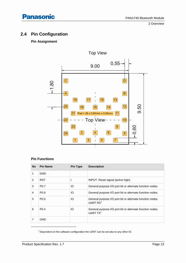
2.4 Pin Configuration
Pin Assignment
Top View
Pin Functions
No Pin Name Pin Type Description
1 GND
2 RST I INPUT. Reset signal (active high).
3 P0.7 IO General purpose I/O port bit or alternate function nodes.
4 P0.6 IO General purpose I/O port bit or alternate function nodes.
5 P0.5 IO General purpose I/O port bit or alternate function nodes.
UART RX1
6 P0.4 IO General purpose I/O port bit or alternate function nodes.
UART TX1
7 GND
1 Dependent on the software configuration the UART can be set also to any other IO.
PAN1740 Bluetooth Module
2 Overview
Product Specification Rev. 1.7 Page 14
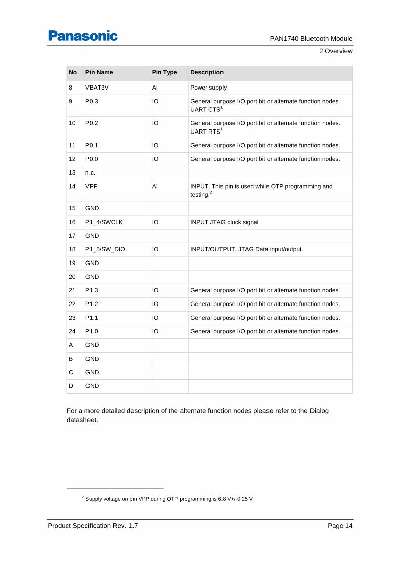
No Pin Name Pin Type Description
8 VBAT3V AI Power supply
9 P0.3 IO General purpose I/O port bit or alternate function nodes.
UART CTS1
10 P0.2 IO General purpose I/O port bit or alternate function nodes.
UART RTS1
11 P0.1 IO General purpose I/O port bit or alternate function nodes.
12 P0.0 IO General purpose I/O port bit or alternate function nodes.
13 n.c.
14 VPP AI INPUT. This pin is used while OTP programming and
testing.2
15 GND
16 P1_4/SWCLK IO INPUT JTAG clock signal
17 GND
18 P1_5/SW_DIO IO INPUT/OUTPUT. JTAG Data input/output.
19 GND
20 GND
21 P1.3 IO General purpose I/O port bit or alternate function nodes.
22 P1.2 IO General purpose I/O port bit or alternate function nodes.
23 P1.1 IO General purpose I/O port bit or alternate function nodes.
24 P1.0 IO General purpose I/O port bit or alternate function nodes.
A GND
B GND
C GND
D GND
For a more detailed description of the alternate function nodes please refer to the Dialog
datasheet.
2 Supply voltage on pin VPP during OTP programming is 6.8 V+/-0.25 V
PAN1740 Bluetooth Module
2 Overview
Product Specification Rev. 1.7 Page 15
2.5 Interfaces
2.5.1 UART
The UART is compliant to the industry-standard 16550 and is used for serial communication
with a peripheral, modem (data carrier equipment, DCE) or data set. Data is written from a
master (CPU) over the APB bus to the UART and it is converted to serial form and transmitted
to the destination device. Serial data is also received by the UART and stored for the master
(CPU) to read back. There is no DMA support on the UART block since its contains internal
FIFOs. Both UARTs support hardware flow control signals (RTS, CTS, DTR, DSR).
Features
• 16 bytes Transmit and receive FIFOs.
• Hardware flow control support (CTS/RTS)
• Shadow registers to reduce software overhead and also include a software programmable reset
• Transmitter Holding Register Empty (THRE) interrupt mode
• IrDA 1.0 SIR mode supporting low power mode.
• Functionality based on the 16550 industry standard:
• Programmable character properties, such as number of data bits per character (5-8), optional
• parity bit (with odd or even select) and number of stop bits (1, 1.5 or 2)
• Line break generation and detection
• Prioritized interrupt identification
• Programmable serial data baud rate as calculated by the following: baud rate = (serial clock frequency)/(divisor).
2.5.2 SPI+
This interface supports a subset of the Serial Peripheral Interface SPI™. The serial interface
can transmit and receive 8, 16 or 32 bits in master/slave mode and transmit 9 bits in master
mode. The SPI+ interface has enhanced functionality with bidirectional 2x16-bit word FIFOs.
SPI™ is a trademark of Motorola, Inc.
Features
• Master and Slave mode
• 8 bit, 9 bit, 16 bit or 32 bit operation
• Clock speeds up to 16 MHz. Programmable output frequencies of SPI source clock divided by 1, 2, 4, 8
• SPI mode 0, 1, 2, 3 support. (clock edge and phase)
• Programmable SPI_DO idle level
• Maskable Interrupt generation
• Bus load reduction by unidirectional writes-only and reads-only modes.
• Built-in RX/TX FIFOs for continuous SPI bursts.
PAN1740 Bluetooth Module
2 Overview
Product Specification Rev. 1.7 Page 16
2.5.3 I2C
The I2C is a programmable control bus that provides support for the communications link
between Integrated Circuits in a system. It is a simple two-wire bus with a software-defined
protocol for system control, which is used in temperature sensors and voltage level translators
to EEPROMs, general-purpose I/O, A/D and D/A converters.
Features
• Two-wire I2C serial interface consists of a serial data line (SDA) and a serial clock (SCL)
• Two speeds are supported:
• Standard mode (0 to 100 Kb/s)
• Fast mode (<= 400 Kb/s)
• Clock synchronization
• 32 deep transmit/receive FIFOs
• Master transmit, Master receive operation
• 7- or 10-bit addressing
• 7- or 10-bit combined format transfers
• Bulk transmit mode
• Default slave address of 0x055
• Interrupt or polled-mode operation
• Handles Bit and Byte waiting at both bus speeds
• Programmable SDA hold time
2.5.4 General Purpose (GP) ADC
The PAN1740 is equipped with a high-speed ultra low power 10-bit general purpose Analog-to-
Digital Converter (GPADC). It can operate in unipolar (single ended) mode as well as in bipolar
(differential) mode. The ADC has its own voltage regulator (LDO) of 1.2 V, which represents the
full scale reference voltage.
Features
• 10-bit dynamic ADC with 65 ns conversion time
• Maximum sampling rate 3.3 Msample/s
• Ultra low power (5 ¬µA typical supply current at 100 ksample/s)
• Single-ended as well as differential input with two input scales
• Four single-ended or two differential external input channels
• Battery monitoring function
• Chopper function
• Offset and zero scale adjust
• Common-mode input level adjust
PAN1740 Bluetooth Module
2 Overview
Product Specification Rev. 1.7 Page 17
2.5.5 Quadrature Decoders
This block decodes the pulse trains from a rotary encoder to provide the step and the direction
of the movement of an external device. Three axes (X, Y, Z) are supported.
The integrated quadrature decoder can automatically decode the signals for the X, Y and Z
axes of a HID input device, reporting step count and direction: the channels are expected to
provide a pulse train with 90 degrees phase difference; depending on whether the reference
channel is leading or lagging, the direction can be determined.
This block can be used for waking up the chip as soon as there is any kind of movement from
the external device connected to it.
Features
• Three 16-bit signed counters that provide the step count and direction on each of the axes (X, Y, and Z)
• Programmable system clock sampling at maximum 16 MHz.
• APB interface for control and programming
• Programmable source from P0, P1 ports
• Digital filter on the channel inputs to avoid spikes
2.5.6 Keyboard Controller
The keyboard controller can be used for debouncing the incoming GPIO signals when
implementing a keyboard scanning engine. It generates an interrupt to the CPU (KEYBR_IRQ).
In parallel, five extra interrupt lines can be triggered by a state change on 32 selectable GPIOs
(GPIOx_IRQ).
Features
• Monitors any of the 12 available GPIOs
• Generates a keyboard interrupt on key press or key release
• Implements debouncing time from 0 up to 63 ms
• Supports five separate interrupt generation lines from GPIO toggling
2.5.7 Input/Output Ports
The PAN1740 has software-configurable I/O pin assignment, organized into ports Port 0, Port1.
Features
• Port 0: 8 pins, Port 1: 6 pins (including SW_CLK and SWDIO)
• Fully programmable pin assignment
• Selectable Push-pull or open drain per pin
• Selectable 25 KOhm pull-up, pull-down resistors per pin
• Pull-up voltage VBAT3V (BUCK mode)
• Fixed assignment for analog pin ADC[3:0]
• Pins retain their last state when system enters the Extended or Deep Sleep mode.
PAN1740 Bluetooth Module
2 Overview
Product Specification Rev. 1.7 Page 18
2.5.8 Timers
For any software-related description please refer to the according Dialog document.
2.5.9 Reset
The PAN1740 comprises an RST pad which is active high. It contains an RC filter for spikes
suppression with 400 kΩ and 2.8 pF for the resistor and the capacitor respectively. It also
contains a 25 kΩ pulldown resistor. This pad should be connected to ground if not needed by
the application. The typical latency of the RST pad is in the range of 2 µs.
PAN1740 Bluetooth Module
3 Detailed Description
Product Specification Rev. 1.7 Page 19
3 Detailed Description
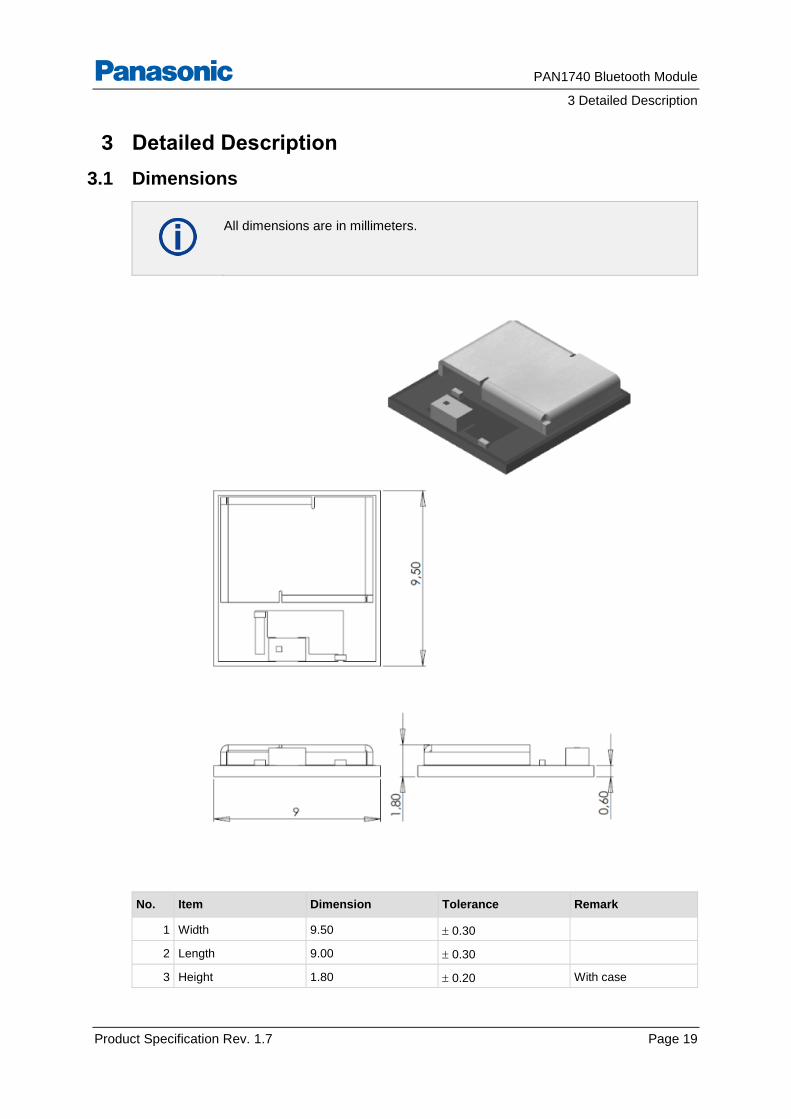
3.1 Dimensions
All dimensions are in millimeters.
No. Item Dimension Tolerance Remark
1 Width 9.50 0.30
2 Length 9.00 0.30
3 Height 1.80 0.20 With case
PAN1740 Bluetooth Module
3 Detailed Description
Product Specification Rev. 1.7 Page 20
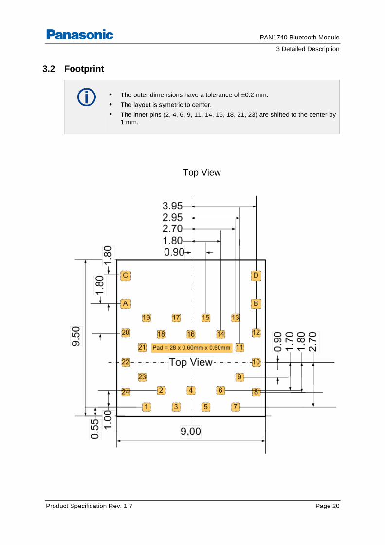
3.2 Footprint
• The outer dimensions have a tolerance of 0.2 mm.
• The layout is symetric to center.
• The inner pins (2, 4, 6, 9, 11, 14, 16, 18, 21, 23) are shifted to the center by 1 mm.
Top View

PAN1740 Bluetooth Module
3 Detailed Description
Product Specification Rev. 1.7 Page 21
3.3 Packaging
The product is a mass production status product and will be delivered in the package described
below.
3.3.1 Tape Dimensions
3.3.2 Packing in Tape
Empty spaces in the component packed area shall be less than two per reel and those spaces
shall not be consecutive.
The top cover tape shall not be found on reel holes and it shall not stick out from the reel.
Measured from centreline of sprocket holeMeasured from centreline of sprocket hole
Cumulative tolerance of 10 sprocket
Measured from centreline of sprocket
to centreline of pocket.
holes is ± 0.20 .
hole to centreline of pocket.
(I)
(II)
(III)
(IV) Other material available.
ALL DIMENSIONS IN MILLIMETRES UNLESS OTHERWISE STATED.W
F
P1
+/- 0.10
+/- 0.10
+/- 0.30
7.50
12.00
16.00
K1 2.00 +/- 0.10
2.80
+/- 0.10
+/- 0.10
9.40Bo
Ko
9.90Ao +/- 0.10
Tooling code: Flatbed - 9 Estimated Max Length: 72m per 22B3
Y
Y
XX
SECTION Y-
Y SCALE 3.5 :
1
SECTION X-
X SCALE 3.5 :
1
trailer (empty)1 x circumference /hub
(min 160mm)
component
packed area
standard
1500pcs
leader (empty)minimum 10 pitch
Top cover tape more
than 1 x
circumference plus
100mm to avoid
fixing of tape end on
sealed modules.
Direction of unreeling (for customer)
PAN1740 Bluetooth Module
3 Detailed Description
Product Specification Rev. 1.7 Page 22
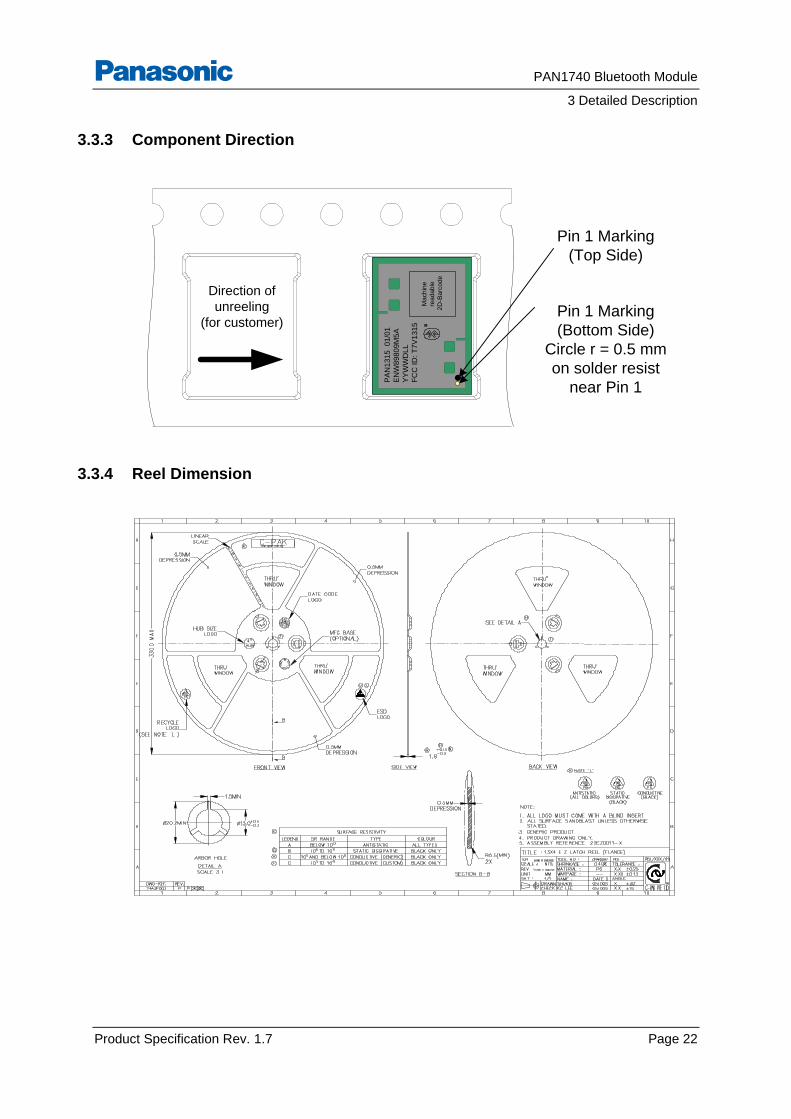
3.3.3 Component Direction
3.3.4 Reel Dimension
PA
N1
31
5
01/0
1
EN
W89809M
5A
YY
WW
DL
L
FC
C I
D: T
7V
1315
Machin
e
readable
2D
-Barc
ode
Direction of
unreeling
(for customer)
Pin 1 Marking
(Top Side)
Pin 1 Marking
(Bottom Side)
Circle r = 0.5 mm
on solder resist
near Pin 1
PAN1740 Bluetooth Module
3 Detailed Description
Product Specification Rev. 1.7 Page 23
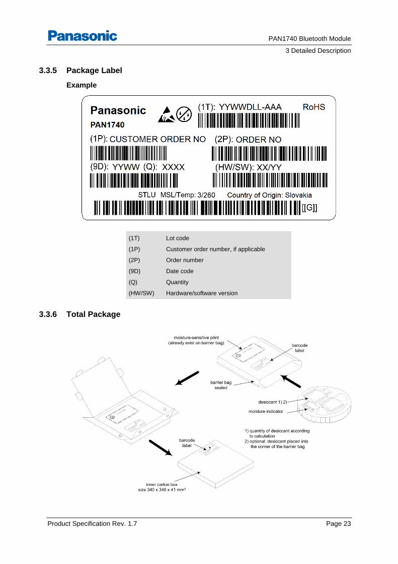
3.3.5 Package Label
Example
(1T)
(1P)
(2P)
(9D)
(Q)
(HW/SW)
Lot code
Customer order number, if applicable
Order number
Date code
Quantity
Hardware/software version
3.3.6 Total Package
PAN1740 Bluetooth Module
3 Detailed Description
Product Specification Rev. 1.7 Page 24
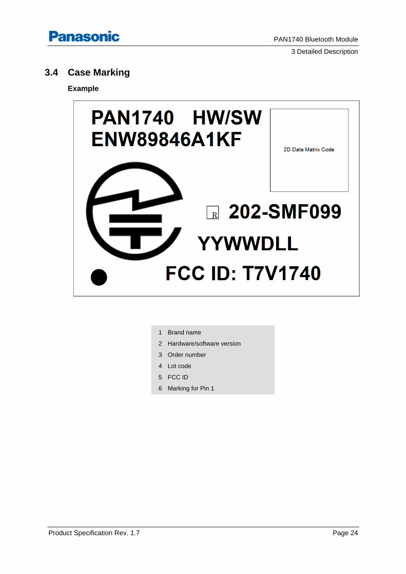
3.4 Case Marking
Example
1
2
3
4
5
6
Brand name
Hardware/software version
Order number
Lot code
FCC ID
Marking for Pin 1
PAN1740 Bluetooth Module
4 Specification
Product Specification Rev. 1.7 Page 25
4 Specification
All specifications are over temperature and process, unless indicated otherwise.
4.1 Default Test Conditions
Temperature: 25 ± 10 °C Humidity: 40 to 85 % RH Supply Voltage: 3.3 V
4.2 Absolute Maximum Ratings
The maximum ratings may not be exceeded under any circumstances, not even momentarily or individually, as permanent damage to the module may result.
The BUCK mode of the DCDC can operate correctly with voltages in the range of 2.2 V upto 3.3 V. If the voltage drops below that, then the OTP might not be readable any more. However, if no OTP is used, then the system is able to further operate up to 1.8 V.
Symbol Parameter Condition Min. Typ. Max. Units
VPIN(LIM)
(default)
limiting voltage
on a pin
Voltage between GND
and VBAT3V
-0.1 VBAT3V
+
0.2
V
TSTG storage
temperature
-50 150 °C
tR(SUP) supply rise time Power supply rise time 100 ms
VBAT(LIM)
(VBAT 3V)
limiting battery
supply voltage
Supply voltage on VBAT3V in a
buck-con- verter application, pin
VBAT1V is connected to ground
1.8/2.2
3.45 V
VESD(HBM)
electrostatic
discharge
voltage (Human
Body Model)
2 000 V
PAN1740 Bluetooth Module
4 Specification
Product Specification Rev. 1.7 Page 26
Symbol Parameter Condition Min. Typ. Max. Units
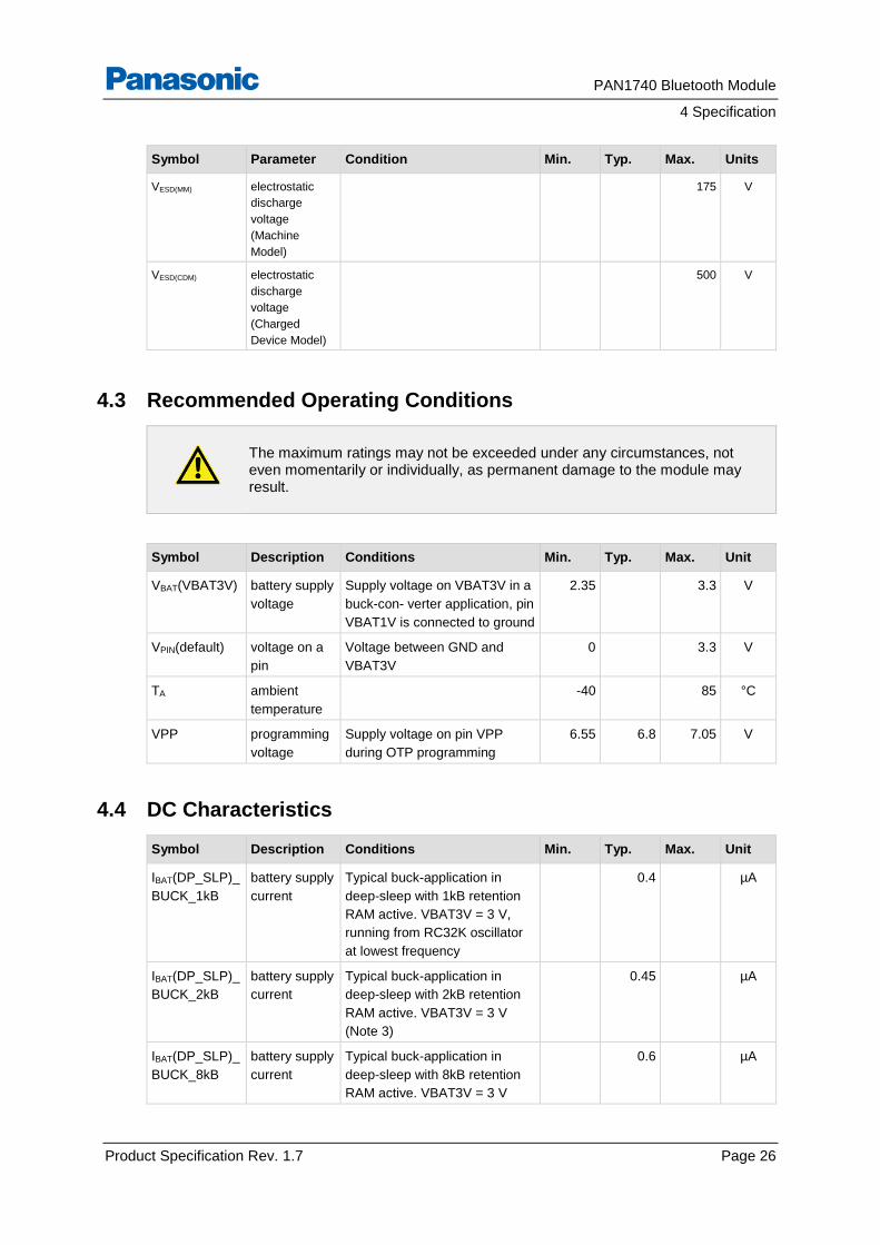
VESD(MM)
electrostatic
discharge
voltage
(Machine
Model)
175 V
VESD(CDM)
electrostatic
discharge
voltage
(Charged
Device Model)
500 V
4.3 Recommended Operating Conditions
The maximum ratings may not be exceeded under any circumstances, not even momentarily or individually, as permanent damage to the module may result.
Symbol Description Conditions Min. Typ. Max. Unit
VBAT(VBAT3V) battery supply
voltage
Supply voltage on VBAT3V in a
buck-con- verter application, pin
VBAT1V is connected to ground
2.35 3.3 V
VPIN(default) voltage on a
pin
Voltage between GND and
VBAT3V
0 3.3 V
TA ambient
temperature
-40 85 °C
VPP programming
voltage
Supply voltage on pin VPP
during OTP programming
6.55 6.8 7.05 V
4.4 DC Characteristics
Symbol Description Conditions Min. Typ. Max. Unit
IBAT(DP_SLP)_
BUCK_1kB
battery supply
current
Typical buck-application in
deep-sleep with 1kB retention
RAM active. VBAT3V = 3 V,
running from RC32K oscillator
at lowest frequency
0.4 µA
IBAT(DP_SLP)_
BUCK_2kB
battery supply
current
Typical buck-application in
deep-sleep with 2kB retention
RAM active. VBAT3V = 3 V
(Note 3)
0.45 µA
IBAT(DP_SLP)_
BUCK_8kB
battery supply
current
Typical buck-application in
deep-sleep with 8kB retention
RAM active. VBAT3V = 3 V
0.6 µA
PAN1740 Bluetooth Module
4 Specification
Product Specification Rev. 1.7 Page 27
Symbol Description Conditions Min. Typ. Max. Unit
IBAT(EXT_SLP)
_BUCK_43KB
battery supply
current
Typical buck-application in
extended-sleep mode with
42 kB (SysRAM) and 1 kB
(RetRAM) retained
1.2 µA
IBAT(EXT_SLP)
_BUCK_50kB
battery supply
current
Typical buck-application in
extended-sleep mode with
42 kB (SysRAM) and 8 kB
(RetRAM) retained
1.4 µA
IBAT(ACT_RX)_
BUCK
battery supply
current
Typical application with buck
converter and receiver active,
VBAT3V = 3.0 V
5.1 mA
IBAT(ACT_TX)_
BUCK
battery supply
current
Typical application with buck
converter and transmitter
active, VBAT3V = 3.0 V
4.8 mA
PBAT
(DP_SLP)
_BUCK_1kB
battery power
consumption
Typical boost-application in
deep-sleep with 1 kB retention
RAM active, running from
RC32K oscillator
1.2 µW
PBAT
(ACT_RX)
_BUCK
battery power
consumption
Typical application with buck
converter, receive mode
15.5 mW
PBAT
(ACT_TX)
_BUCK
battery power
consumption
Typical application with buck
converter, transmit mode
14.3 mW
4.5 MHz Crystal Oscillator: Timing Characteristics
Symbol Description Conditions Min. Typ. Max. Unit
tSTA(XTAL)(16M) crystal
oscillator
startup time
0.5 2 3 ms
4.6 32 kHz Crystal Oscillator: Timing Characteristics
Symbol Description Conditions Min. Typ. Max. Unit
tSTA(XTAL)(32k) crystal
oscillator
startup time
Typical application, time until
1 000 clocks are detected
0.4 s
4.7 DC-DC Converter: DC Characteristics
Symbol Description Conditions Min. Typ. Max. Unit
VO(BUCK) output voltage default settings 1.41 V
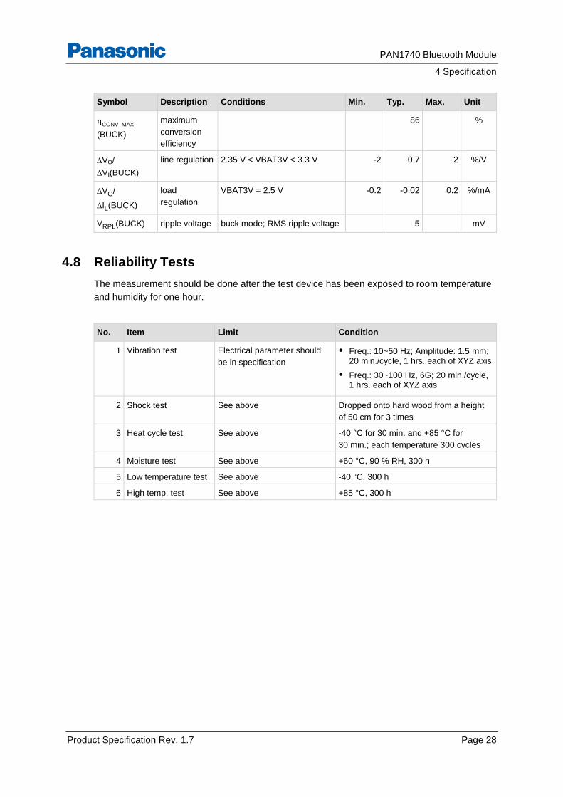
PAN1740 Bluetooth Module
4 Specification
Product Specification Rev. 1.7 Page 28
Symbol Description Conditions Min. Typ. Max. Unit
CONV_MAX
(BUCK)
maximum
conversion
efficiency
86 %
VO/
VI(BUCK)
line regulation 2.35 V < VBAT3V < 3.3 V -2 0.7 2 %/V
VO/
IL(BUCK)
load
regulation
VBAT3V = 2.5 V -0.2 -0.02 0.2 %/mA
VRPL(BUCK) ripple voltage buck mode; RMS ripple voltage 5 mV
4.8 Reliability Tests
The measurement should be done after the test device has been exposed to room temperature
and humidity for one hour.
No. Item Limit Condition
1 Vibration test Electrical parameter should
be in specification
• Freq.: 10~50 Hz; Amplitude: 1.5 mm; 20 min./cycle, 1 hrs. each of XYZ axis
• Freq.: 30~100 Hz, 6G; 20 min./cycle, 1 hrs. each of XYZ axis
2 Shock test See above Dropped onto hard wood from a height
of 50 cm for 3 times
3 Heat cycle test See above -40 °C for 30 min. and +85 °C for
30 min.; each temperature 300 cycles
4 Moisture test See above +60 °C, 90 % RH, 300 h
5 Low temperature test See above -40 °C, 300 h
6 High temp. test See above +85 °C, 300 h
PAN1740 Bluetooth Module
4 Specification
Product Specification Rev. 1.7 Page 29
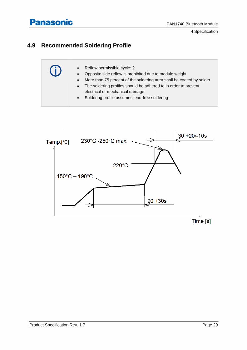
4.9 Recommended Soldering Profile
Reflow permissible cycle: 2
Opposite side reflow is prohibited due to module weight
More than 75 percent of the soldering area shall be coated by solder
The soldering profiles should be adhered to in order to prevent
electrical or mechanical damage
Soldering profile assumes lead-free soldering
PAN1740 Bluetooth Module
5 Cautions
Product Specification Rev. 1.7 Page 30
5 Cautions
Failure to follow the guidelines set forth in this document may result in degrading of the product’s functions and damage to the product.
5.1 Design Notes
1. Follow the conditions written in this specification, especially the control signals of this
module.
2. The supply voltage must be free of AC ripple voltage (for example from a battery or a low
noise regulator output). For noisy supply voltages, provide a decoupling circuit (for
example a ferrite in series connection and a bypass capacitor to ground of at least 47 µF
directly at the module).
3. This product should not be mechanically stressed when installed.
4. Keep this product away from heat. Heat is the major cause of decreasing the life of these
products.
5. Avoid assembly and use of the target equipment in conditions where the product’s
temperature may exceed the maximum tolerance.
6. The supply voltage should not be exceedingly high or reversed. It should not carry noise
and/or spikes.
7. Keep this product away from other high frequency circuits.
8. Refer to the recommended pattern when designing a board.
5.2 Installation Notes
1. Reflow soldering is possible twice based on the conditions set forth in 4.9
Recommended Soldering Profile. Set up the temperature at the soldering portion of this
product according to this reflow profile.
2. Carefully position the products so that their heat will not burn into printed circuit boards
or affect the other components that are susceptible to heat.
3. Carefully locate these products so that their temperatures will not increase due to the
effects of heat generated by neighboring components.
4. If a vinyl-covered wire comes into contact with the products, then the cover will melt and
generate toxic gas, damaging the insulation. Never allow contact between the cover and
these products to occur.
5. This product should not be mechanically stressed or vibrated when reflowed.
6. To repair the board by hand soldering, follow the conditions set forth in this chapter.
7. Do not wash this product.
8. Pressing on parts of the metal cover or fastening objects to the metal will cause damage
to the unit.
PAN1740 Bluetooth Module
5 Cautions
Product Specification Rev. 1.7 Page 31
5.3 Usage Condition Notes
1. Take measures to protect the unit against static electricity.
If pulses or other transient loads (a large load applied in a short time) are applied to the
products, check and evaluate their operation befor assembly on the final products.
2. Do not use dropped products.
3. Do not touch, damage or soil the pins.
4. Follow the recommended condition ratings about the power supply applied to this
product.
5. Electrode peeling strength: Do not add pressure of more than 4.9 N when soldered on
PCB.
6. Pressing on parts of the metal cover or fastening objects to the metal cover will cause
damage.
7. These products are intended for general purpose and standard use in general electronic
equipment, such as home appliances, office equipment, information, and communication
equipment.
5.4 Storage Notes
1. The module should not be stressed mechanically during storage.
2. Do not store these products in the following conditions or the performance
characteristics of the product, such as RF performance will be adversely affected:
– Storage in salty air or in an environment with a high concentration of corrosive gas,
such as Cl2, H2S, NH3, SO2, or NOX,
– Storage in direct sunlight,
– Storage in an environment where the temperature may be outside the range of 5 °C to
35 °C, or where the humidity may be outside the 45 to 85 percent range,
– Storage of the products for more than one year after the date of delivery storage period:
Please check the adhesive strength of the embossed tape and soldering after 6 months
of storage.
3. Keep this product away from water, poisonous gas, and corrosive gas.
4. This product should not be stressed or shocked when transported.
5. Follow the specification when stacking packed crates (max. 10).
5.5 Safety Cautions
These specifications are intended to preserve the quality assurance of products and individual
components.
Before use, check and evaluate the operation when mounted on your products. Abide by these
specifications without deviation when using the products. These products may short-circuit. If
electrical shocks, smoke, fire, and/or accidents involving human life are anticipated when a
short circuit occurs, provide the following failsafe functions as a minimum:
PAN1740 Bluetooth Module
5 Cautions
Product Specification Rev. 1.7 Page 32
1. Ensure the safety of the whole system by installing a protection circuit and a protection
device.
2. Ensure the safety of the whole system by installing a redundant circuit or another system
to prevent a single fault causing an unsafe status.
5.6 Other Cautions
1. Do not use the products for other purposes than those listed.
2. Be sure to provide an appropriate fail-safe function on your product to prevent any
additional damage that may be caused by the abnormal function or the failure of the
product.
3. This product has been manufactured without any ozone chemical controlled under the
Montreal Protocol.
4. These products are not intended for uses other than under the special conditions shown
below. Before using these products under such special conditions, carefully check their
performance and reliability under the said special conditions to determine whether or not
they can be used in such a manner:
– In liquid, such as water, salt water, oil, alkali, or organic solvent, or in places where
liquid may splash,
– In direct sunlight, outdoors, or in a dusty environment,
– In an environment where condensation occurs,
– In an environment with a high concentration of harmful gas (e. g. salty air, HCl, Cl2,
SO2, H2S, NH3, and NOX).
5. If an abnormal voltage is applied due to a problem occurring in other components or
circuits, replace these products with new products because they may not be able to
provide normal performance even if their electronic characteristics and appearances
appear satisfactory.
6. When you have any question or uncertainty, contact Panasonic.
5.7 Life Support Policy
This Panasonic Industrial Devices Europe GmbH product is not designed for use in life support
appliances, devices, or systems where malfunction can reasonably be expected to result in a
significant personal injury to the user, or as a critical component in any life support device or
system whose failure to perform can be reasonably expected to cause the failure of the life
support device or system, or to affect its safety or effectiveness.
Panasonic customers using or selling these products for use in such applications do so at their
own risk and agree to fully indemnify Panasonic Industrial Devices Europe GmbH for any
damages resulting.
PAN1740 Bluetooth Module
6 Regulatory and Certification Information
Product Specification Rev. 1.7 Page 33
6 Regulatory and Certification Information
6.1 Federal Communications Commission (FCC) for US
6.1.1 FCC Notice
The PAN1740 including the antennas, which are listed in 6.1.5 Approved Antenna List, complies with Part 15 of the FCC Rules.
The device meets the requirements for modular transmitter approval as detailed in FCC public
Notice DA00-1407. The transmitter operation is subject to the following two conditions:
1. This device may not cause harmful interference, and
2. This device must accept any interference received, including interference that may
cause undesired operation.
6.1.2 Caution
The FCC requires the user to be notified that any changes or modifications made to this device that are not expressly approved by Panasonic Industrial Devices Europe GmbH may void the user's authority to operate the equipment.
This equipment has been tested and found to comply with the limits for a Class B digital device, pursuant to Part 15 of the FCC Rules.
These limits are designed to provide reasonable protection against harmful interference in a residential installation. This equipment generates uses and can radiate radio frequency energy and, if not installed and used in accordance with the instructions, may cause harmful interference to radio communications.
However, there is no guarantee that interference will not occur in a particular installation. If this
equipment does cause harmful interference to radio or television reception, which can be
determined by turning the equipment off and on, the user is encouraged to try to correct the
interference by one or more of the following measures:
• Reorient or relocate the receiving antenna.
• Increase the separation between the equipment and receiver.
• Connect the equipment into an outlet on a circuit different from that to which the receiver is connected.
• Consult the dealer or an experienced radio/TV technician for help

PAN1740 Bluetooth Module
6 Regulatory and Certification Information
Product Specification Rev. 1.7 Page 34
6.1.3 Label Requirements
The OEM must ensure that FCC labelling requirements are met. This includes a clearly visible label on the outside of the OEM enclosure specifying the appropriate Panasonic FCC identifier for this product as well as the FCC Notice above.
The FCC identifier is FCC ID: T7V1740.
This FCC identifier is valid for the PAN1740. The end product must in any case be labelled on
the exterior with:
"Contains FCC ID: T7V1740"
6.1.4 Antenna Warning
This antenna warning refers to the test device with the model number PAN1740 Chapter 7.1
Ordering Information
The device is tested with a standard SMA connector and with the antenna listed below. When
integrated into the OEM’s product, these fixed antennas require installation preventing end
users from replacing them with non-approved antennas. Any antenna not in the following table
must be tested to comply with FCC Section 15.203 for unique antenna connectors and with
Section 15.247 for emissions. The FCC identifier for the device with the antenna listed in
6.1.5 Approved Antenna List is the same (FCC ID: T7V1740).
6.1.5 Approved Antenna List
Item Part Number Manufacturer Frequency Band Type Gain (dBi)
1 LDA212G3110K Murata 2.4 GHz Chip antenna +0.9
2 ANT2012 Yageo 2.4GHz Chip-Antenna +0.9
PAN1740 Bluetooth Module
6 Regulatory and Certification Information
Product Specification Rev. 1.7 Page 35
6.1.6 RF Exposure
To comply with FCC RF Exposure requirements, the OEM must ensure that only antennas from the Approved Antenna List are installed 6.1.5 Approved Antenna List.
The preceding statement must be included as a CAUTION statement in manuals for products operating with the approved antennas in the previous table to alert users on FCC RF Exposure compliance.
Any notification to the end user of installation or removal instructions about the integrated radio module is not allowed.
The radiated output power of the PAN1740 with a mounted ceramic antenna (FCC ID: T7V1740) is below the FCC radio frequency exposure limits. Nevertheless, the PAN1740 shall be used in such a manner that the potential for human contact during normal operation is minimized.
End users may not be provided with the module installation instructions. OEM integrators and end users must be provided with transmitter operating conditions for satisfying RF exposure compliance.
6.2 Industry Canada Certification
English
The PAN1740 is licensed to meet the regulatory requirements of Industry Canada (IC).
License ID: IC: 216Q-1740
Manufacturers of mobile, fixed or portable devices incorporating this module are advised to
clarify any regulatory questions and ensure compliance for SAR and/or RF exposure limits.
Users can obtain Canadian information on RF exposure and compliance from www.ic.gc.ca.
This device has been designed to operate with the antennas listed in 6.1.5 Approved
Antenna List, having a maximum gain of +0.9 dBi. Antennas not included in this list or having a
gain greater than +0.9 dBi are strictly prohibited for use with this device. The required antenna
impedance is 50 ohms. The antenna used for this transmitter must not be co-located or
operating in conjunction with any other antenna or transmitter.
Due to the model size, the IC identifier is displayed in the installation instruction only and it
cannot be displayed on the module’s label due to the limited size (8.7 x 15.6 mm).
PAN1740 Bluetooth Module
6 Regulatory and Certification Information
Product Specification Rev. 1.7 Page 36
French
PAN1740 est garanti conforme aux dispositions règlementaires d’Industry Canada (IC).
License: IC: 216Q-1740
Il est recommandé aux fabricants d’appareils fixes, mobiles ou portables de consulter la
réglementation en vigueur et de vérifier la conformité de leurs produits relativement aux limites
d’exposition aux rayonnements radiofréquence ainsi qu’au débit d’absorption spécifique
maximum autorisé.
Des informations pour les utilisateurs sur la réglementation Canadienne concernant l’exposition
aux rayonnements RF sont disponibles sur le site www.ic.gc.ca.
Ce produit a été développé pour fonctionner spécifiquement avec les antennes listées dans le
tableau 6.1.5 Approved Antenna List, présentant un gain maximum de 0.9 dBi. Des antennes
autres que celles listées ici, ou présentant un gain supérieur à 0.9 dBi ne doivent en aucune
circonstance être utilisées en combinaison avec ce produit. L’impédance des antennes
compatibles est 50 Ohm. L’antenne utilisée avec ce produit ne doit ni être située à proximité
d’une autre antenne ou d’un autre émetteur, ni être utilisée conjointement avec une autre
antenne ou un autre émetteur.
En raison de la taille du produit, l’identifiant IC est fourni dans le manuel d’installation.
6.2.1 IC Notice
English
The device PAN1740 ( 7.1 Ordering Information), including the antennas ( 6.1.5 Approved Antenna List), complies with Canada RSS-GEN Rules. The device meets the requirements for modular transmitter approval as detailed in RSS-Gen.
Operation is subject to the following two conditions:
1. This device may not cause harmful interference, and
2. This device must accept any interference received, including interference that may
cause undesired operation.
French
Le présent appareil PAN1740 ( 7.1 Ordering Information), les antennes y compris ( 6.1.5 Approved Antenna List), est conforme aux CNR-Gen d'Industrie Canada applicables aux appareils radio exempts de licence.
L'exploitation est autorisée aux deux conditions suivantes :
1. l'appareil ne doit pas produire de brouillage, et
2. l'utilisateur de l'appareil doit accepter tout brouillage radioélectrique subi, même si le
brouillage est susceptible d'en compromettre le fonctionnement.
PAN1740 Bluetooth Module
6 Regulatory and Certification Information
Product Specification Rev. 1.7 Page 37
6.2.2 Labeling Requirements
English
Labeling Requirements
The OEM must ensure that IC labelling requirements are met. This includes a clearly visible label on the outside of the OEM enclosure specifying the appropriate Panasonic IC identifier for this product as well as the IC Notice above.
The IC identifier is:
IC: 216Q-1740
This IC identifier is valid for all PAN1740 modules 7.1 Ordering Information. In any case, the end product must be labelled on the exterior with:
"Contains IC: 216Q-1740”.
French
Obligations d’étiquetage
Les fabricants d’équipements d’origine (FEO) – en anglais Original Equipment Manufacturer (OEM) – doivent s’assurer que les obligations d’étiquetage IC du produit final sont remplies. Ces obligations incluent une étiquette clairement visible à l’extérieur de l’emballage externe, comportant l’identifiant IC du module Panasonic inclus, ainsi que la notification ci-dessus.
L’ identifiant IC est:
IC: 216Q-1740
Cet identifiant est valide pour tous les modules PAN1740 7.1 Ordering Information. Dans tous les cas les produits finaux doivent indiquer sur leur emballage externe la mention suivante:
"Contient IC: 216Q-1740”.
6.3 Japanese Radio Law Compliance
This device is granted pursuant to the Japanese Radio Law (電波法).
This device should not be modified (otherwise the granted designation number will become
invalid).
The MIC ID is: [R]202-SMF099
PAN1740 Bluetooth Module
6 Regulatory and Certification Information
Product Specification Rev. 1.7 Page 38
6.4 European Conformity According to RED (2014/53/EU)
All modules described in this Product Specification comply with the standards according to the
following LVD (2014/35/EU), EMC-D (2014/30/EU) together with the RED (2014/53/EU) articles:
3.1a Safety/Health: EN60950-1:2006+A11:2009+A1:2010+A12:2011+AC:2011+A2:2013
EN62311:2008
3.1b EMC: EN 301 489-1 V2.1.1:2017-02
EN 301 489-17 V3.1.1:2017-02
3.2 Radio: EN 300 328 V2.1.1:2016-11
As a result of the conformity assessment procedure described in the 2014/53/EU Directive, the
end customer equipment should be labelled as follows:
PAN1740 in the specified reference design can be used in all countries of the European
Economic Area (Member States of the EU, European Free Trade Association States [Iceland,
Liechtenstein, Norway]), Monaco, San Marino, Andorra and Turkey.
6.5 Bluetooth
The final Bluetooth product needs to be created by using the following IDs:
QDID Declaration ID
Controller Subsystem 50800 B021655
Profile Subsystem 51591 B021941
Host SubSystem 51910 B021835
6.6 RoHS and REACH Declaration
The latest declaration of environmental compatibility (RoHS and REACH) for supplied products
can be found on the Panasonic website in the “Downloads” section of the respective product
7.2.2 Product Information.
PAN1740 Bluetooth Module
7 Appendix
Product Specification Rev. 1.7 Page 39
7 Appendix
7.1 Ordering Information
Variants and Versions
Order Number Brand Name Description MOQ3
ENW89846A1KF4 PAN1740 PAN1740 Bluetooth Low Energy Module 1 500
3 Abbreviation for Minimum Order Quantity (MOQ). The default MOQ for mass production is 1 500 pieces, fewer only on customer demand. Samples for evaluation can be delivered at any quantity via the distribution channels.
4 Samples are available on customer demand.
PAN1740 Bluetooth Module
7 Appendix
Product Specification Rev. 1.7 Page 40
7.2 Contact Details
7.2.1 Contact Us
Please contact your local Panasonic Sales office for details on additional product options and
services:
For Panasonic Sales assistance in the EU, visit
https://eu.industrial.panasonic.com/about-us/contact-us
Email: [email protected]
For Panasonic Sales assistance in North America, visit the Panasonic Sales & Support Tool to
find assistance near you at
https://na.industrial.panasonic.com/distributors
Please visit the Panasonic Wireless Technical Forum to submit a question at
https://forum.na.industrial.panasonic.com
7.2.2 Product Information
Please refer to the Panasonic Wireless Connectivity website for further information on our
products and related documents:
For complete Panasonic product details in the EU, visit
http://pideu.panasonic.de/products/wireless-modules.html
For complete Panasonic product details in North America, visit
http://www.panasonic.com/rfmodules


![2012[1].10.08 BTLE PT Corporate Presentation English PRINT](https://img.pdfslide.net/doc/110x75/577cd99f1a28ab9e78a3c348/201211008-btle-pt-corporate-presentation-english-print.jpg)