Embed Size (px)
Citation preview
Paper ReviewAvelino Zepeda Martinez
High Performance Reconfigurable Pipelined
Matrix Multiplication Module Designer

• Usage– Communication Systems– Signal and Video Processing
• Issues– Operations of square matrices increase as
functions of n3
Area Speed Power
2.- Background
• For the multiplication of an m*r matrix and an r*n matrix the result is found with:
• Number of multiplications, M, and additions, A, increase with matrices sizes
3.- Matrix Multiplication
• Matrices sizes set to:
• Simplifies multiplication to:
• Where:
4.- Matrix Multiplication (Cont.)

• Basic Matrix Multiplication block using dt
• Can perform any matrix multiplication– Inefficient
5.- Matrix Multiplication (Cont.)

• Three types of errors– Number Representation
ADCs Sampling Rate Available Bits
– Rounding Error Round to Nearest Even (RNE) Round Towards Zero, or Truncation (TRA) Round Down (Floor) Round Up (Ceiling) Round Away from Zero
– Algorithm/Design Error
6.- Error Analysis

7.- Error Analysis (Cont.)
• Reconfigurable Matrix Multiplication Module Designer (RMD)
– Designed in Pearl scripting language
– Outputs: RTL of Multiplication Module Testbench MATLAB files Modelsim verification files
– Designed to output RTL for FPGA and VLSI
8.- Design Overview

• Three main sections– Module Designer– Area, Speed, and Error Analysis– High Speed Memory Interface
9.- RMD FPGA Design Flow
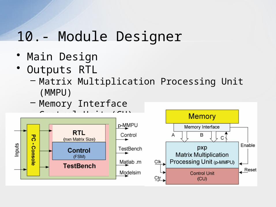
• Main Design• Outputs RTL
– Matrix Multiplication Processing Unit (MMPU)– Memory Interface– Control Unit (CU)
10.- Module Designer
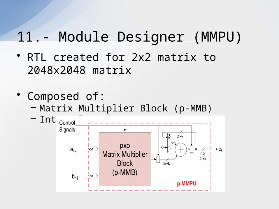
• RTL created for 2x2 matrix to 2048x2048 matrix
• Composed of:– Matrix Multiplier Block (p-MMB)– Internal Logic
11.- Module Designer (MMPU)

• Bottom-Up Design Approach• Start with 2-MMB, or 2X2, which is the
pipelined version of dt
• Insert adders after 2-MMB blocks
12.- Module Designer (p-MMB)
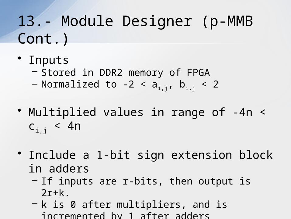
• Inputs– Stored in DDR2 memory of FPGA– Normalized to -2 < ai,j, bi,j < 2
• Multiplied values in range of -4n < ci,j < 4n
• Include a 1-bit sign extension block in adders– If inputs are r-bits, then output is 2r+k.– k is 0 after multipliers, and is incremented by 1
after adders
13.- Module Designer (p-MMB Cont.)

• Input values are represented with Integer bits and Fraction bits
• Inputs are fixed point and normalized, therefore
• Output is stored in memory– (2r+10)-bit, (2x+10, 2y)– Rounded back to r-bit using RNE
14.- Module Designer (Memory Interface)

• Can be created for Fixed or Variable Operation Size
• Designed to use Finite State Machine
• For variable size each operation size has a sub-FSM
15.- Module Designer (Control Unit)

• RMD also generates MATLAB and Testbench files– Improves accuracy of output Matrix– Reduces design and verification time
• MATLAB creates data files for the Testbench– Maximum input values supported
Bit size: 64 bits Matrix Size: 2048x2048 Test Vectors: 100
• Data tested on Testbench using Modelsim
16.- Area, Speed, and Error Analysis

• Output data is compared with actual values obtained from MATLAB
• Errors obtained:– Absolute Error (ε)
– Relative Error (η)
– Rounding Error(μ)
– Total Rounding Error (μtotal)
17.- Area, Speed, and Error Analysis (Cont.)

• RMD calculates the estimated area– Area = Matrix Multiplier Block + Memory + Control
• These calculations use:– n :Maximum Matrix Multiplication Size– r :Input bits– p :Matrix Multiplier Block Size– Mr :r-bit Multiplier– Ar :r-bit Adder– Rr :r-bit Register– Muxr :r-bit (2-1) Mux– RNE :(2r+kmax to r) bit Rounding– HA :Half Adder– Memr :r-bit Memory– FF :Flip Flops– Fmax :Maximum Frequency
18.- Area, Speed, and Error Analysis (Cont.)

• Matrix Multiplier Block Area
19.- Area, Speed, and Error Analysis (Cont.)

• Memory Area
• Control Unit Area
20.- Area, Speed, and Error Analysis (Cont.)

• Latency
• Time
21.- Area, Speed, and Error Analysis (Cont.)

• Two Native Port Interfaces– Interface with DDR2 memory– Width of 64 bits– Supports Back-to-Back Transfers– Transfer Sizes:
Byte Half-word Word 4-word and 8-word cache line 16-word, 32-word, and 64-word bursts
22.-High Speed Memory Interface

23.- Area Results (Spartan 3E)

24.- Area Results (Virtex-5)

25.- Time Results

• Design Pipelined– Increase Throughput and Reduce Operation
Latency
• Incremental Adder– Reduce Area and Increase Accuracy
• Modifiable– Increased Accuracy– Faster Operation– Lower Area
26.- Conclusion