Embed Size (px)
Citation preview

LEBANESE AMERICAN UNIVERSITY
Parallel Multi-Voltage Power Minimization
in VLSI Circuits
By
RABIH HALIM YOUNES
A thesis
Submitted in partial fulfillment of the requirements
for the degree of Master of Science in Computer Engineering
School of Engineering
August 2013

ii
Signatures Redacted
Signatures Redacted
Signatures Redacted

iii
Signatures Redacted
Signatures Redacted
Signatures Redacted
Signatures Redacted

iv
Signatures RedactedSignatures Redacted
Signatures Redacted

v
Signatures Redacted

vi
Signatures Redacted

vii
ACKNOWLEDGEMENTS
This research would not have been possible without the help and assistance of many
persons.
First I would like to express my gratitude to my supervisor Dr. Iyad Ouaiss.
I am also deeply grateful to Dr. Zahi Nakad and Dr. Dani Tannir for being on my
thesis committee.
Finally, special thanks go also to my friends and family for their long support.

viii
To my loving friends and family

ix
Parallel Multi-Voltage Power Minimization
in VLSI Circuits
Rabih Halim Younes
Abstract
Power consumption minimization is nowadays considered a main challenge to VLSI
designers, especially with the growth of the mobile computing industry. Previous
studies have tried minimizing power consumption at the expense of the overall
circuit delay, and have mostly focused at optimizing power at the lower levels of
abstraction – during placement and routing. This work presents novel techniques to
minimize power consumption during behavioral synthesis and to reduce execution
runtime through parallel processing. Design space exploration at higher levels of
abstraction yields greater optimization in power, area, and delay; thus, the first
contribution intelligently reduces voltages of non-critical paths in order to decrease
total power consumption at the behavioral level. Voltage reductions are performed
while minimizing the number of voltage conversions introduced in the circuit and
maintaining the critical path delay. The second contribution concentrates on
exploiting parallelism by distributing independent synthesis tasks to different
processing units in the goal of reducing solution exploration time.
A synthesis software suite was implemented to test the proposed approaches. Power
consumption was reduced considerably with a negligible overhead of voltage
conversion modules. Furthermore, design space exploration time declined
significantly due to the use of parallel programming.
Keywords: Multi-Voltage, Power Consumption Minimization, High-Level Synthesis,
Parallel Programming.

x
TABLE OF CONTENTS
CHAPTER ONE .......................................................................................................... 1
INTRODUCTION ....................................................................................................... 1
CHAPTER TWO ......................................................................................................... 3
LITERATURE REVIEW............................................................................................. 3
2.1. High-level synthesis ...................................................................................... 3
2.1.1. Scheduling .............................................................................................. 8
2.1.2. Binding ................................................................................................. 19
2.2. Previous work .............................................................................................. 23
CHAPTER THREE .................................................................................................... 25
PARALLEL MULTI-VOLTAGE POWER MINIMIZATION................................. 25
3.1. Multi-voltage power minimization .............................................................. 25
3.1.1. Challenges ............................................................................................ 26
3.1.2. Overcoming challenges and improving previous works ...................... 33
3.1.3. Power minimization approach ............................................................. 38
3.2. Parallel multi-voltage power minimization ................................................. 45
CHAPTER FOUR ...................................................................................................... 47
EXPERIMENTAL RESULTS ................................................................................... 47
4.1. Technology metrics ..................................................................................... 47
4.2. Benchmarks ................................................................................................. 48
4.2.1. HAL: .................................................................................................... 49

xi
4.2.2. ARF: ..................................................................................................... 50
4.2.3. EWF: .................................................................................................... 51
4.2.4. FIR1: .................................................................................................... 53
4.2.5. FIR: ...................................................................................................... 55
4.2.6. COS1: ................................................................................................... 56
4.2.7. COS2: ................................................................................................... 57
4.3. Results and analysis ..................................................................................... 58
4.3.1. Power saving results for designs without reuse ................................... 58
4.3.2. Power saving results for designs with reuse ........................................ 68
4.3.3. Effects of amplifiers on the area .......................................................... 80
4.3.4. Speedup results .................................................................................... 81
CHAPTER FIVE ........................................................................................................ 89
CONCLUSIONS AND FUTURE WORK ................................................................ 89
BIBLIOGRAPHY ...................................................................................................... 91
APPENDIX I .............................................................................................................. 94
THE SYNTHESIS SOFTWARE SUITE .................................................................. 94

xii
LIST OF TABLES
Table 1: Available resources ...................................................................................... 17
Table 2: 2-input AND gate delay ............................................................................... 27
Table 3: 2-input OR gate delay .................................................................................. 28
Table 4: 2-input XOR gate delay ............................................................................... 29
Table 5: Full adder delay............................................................................................ 30
Table 6: Opportunities for power saving (Pedram, 1999).......................................... 38
Table 7: Technologies used ........................................................................................ 48
Table 8: Power savings for designs without reuse (optimal α, β and γ parameters) .. 58
Table 9: Power savings for designs with reuse and unlimited resources ................... 68
Table 10: Modifying the available number of multipliers while other resources are
unlimited (HAL)......................................................................................................... 70
Table 11: Modifying the available number of adders while other resources are
unlimited (HAL)......................................................................................................... 70
Table 12: Modifying the available number of multipliers while other resources are
unlimited (ARF) ......................................................................................................... 72
Table 13: Modifying the available number of adders while other resources are
unlimited (ARF) ......................................................................................................... 72
Table 14: Modifying the available number of multipliers while other resources are
unlimited (EWF) ........................................................................................................ 73
Table 15: Modifying the available number of adders while other resources are
unlimited (EWF) ........................................................................................................ 73
Table 16: Modifying the available number of multipliers while other resources are
unlimited (FIR1) ........................................................................................................ 74

xiii
Table 17: Modifying the available number of adders while other resources are
unlimited (FIR1) ........................................................................................................ 74
Table 18: Modifying the available number of multipliers while other resources are
unlimited (FIR) .......................................................................................................... 75
Table 19: Modifying the available number of adders while other resources are
unlimited (FIR) .......................................................................................................... 75
Table 20: Modifying the available number of multipliers while other resources are
unlimited (COS1) ....................................................................................................... 77
Table 21: Modifying the available number of adders while other resources are
unlimited (COS1) ....................................................................................................... 77
Table 22: Modifying the available number of multipliers while other resources are
unlimited (COS2) ....................................................................................................... 78
Table 23: Modifying the available number of adders while other resources are
unlimited (COS2) ....................................................................................................... 78
Table 24: The effects of the added amplifiers on the total design area...................... 80
Table 25: Speedup with 2 threads .............................................................................. 81
Table 26: Speedup with 4 threads .............................................................................. 82
Table 27: Speedup with 8 threads .............................................................................. 83

xiv
LIST OF FIGURES
Figure 1: CDFG of the differential equation problem ................................................. 7
Figure 2: ASAP scheduling algorithm (Gajski et al., 1992) ...................................... 10
Figure 3: ASAP scheduled differential circuit ........................................................... 11
Figure 4: ALAP scheduling algorithm (Gajski et al., 1992) ...................................... 12
Figure 5: ALAP scheduled differential circuit ........................................................... 13
Figure 6: Delaying nodes on the critical path increases total latency ........................ 15
Figure 7: List scheduling algorithm (Gajski et al., 1992) .......................................... 16
Figure 8: List scheduled differential circuit ............................................................... 18
Figure 9: Left-Edge algorithm (De Micheli, 1994) .................................................... 20
Figure 10: Scheduled CDFG ...................................................................................... 21
Figure 11: Multiplier and ALU compatibility graphs ................................................ 22
Figure 12: 2-input AND gate delay vs. voltage ......................................................... 27
Figure 13: 2-input OR gate delay vs. voltage ............................................................ 28
Figure 14: 2-input XOR gate delay vs. voltage.......................................................... 29
Figure 15: Full adder .................................................................................................. 30
Figure 16: Full adder delay vs. voltage ...................................................................... 31
Figure 17: Direct compensation amplifier (Baker, 2013) .......................................... 36
Figure 18: Indirect compensation amplifier (Baker, 2013) ........................................ 36
Figure 19: Differential amplifier (Allen et al., 2011)................................................. 37
Figure 20: Push-pull common source amplifier (Allen et al., 2011) ......................... 37
Figure 21: Power minimization algorithm for designs without reuse ........................ 40
Figure 22: Power minimization algorithm for designs with reuse ............................. 42
Figure 23: The parallel algorithm .............................................................................. 45

xv
Figure 24: HAL benchmark DFG .............................................................................. 49
Figure 25: ARF benchmark DFG ............................................................................... 50
Figure 26: EWF benchmark DFG .............................................................................. 51
Figure 27: FIR1 benchmark DFG .............................................................................. 53
Figure 28: FIR benchmark DFG ................................................................................ 55
Figure 29: COS1 benchmark DFG ............................................................................. 56
Figure 30: COS2 benchmark DFG ............................................................................. 57
Figure 31: HAL power savings for different α, β and γ parameters (no reuse) ......... 60
Figure 32: ARF power savings for different α, β and γ parameters (no reuse) .......... 61
Figure 33: EWF power savings for different α, β and γ parameters (no reuse) ......... 62
Figure 34: FIR1 power savings for different α, β and γ parameters (no reuse) ......... 63
Figure 35: FIR power savings for different α, β and γ parameters (no reuse) ........... 64
Figure 36: COS1 power savings for different α, β and γ parameters (no reuse) ........ 65
Figure 37: COS2 power savings for different α, β and γ parameters (no reuse) ........ 66
Figure 38: HAL speedup vs. number of threads ........................................................ 84
Figure 39: ARF speedup vs. number of threads ......................................................... 84
Figure 40: FIR1 speedup vs. number of threads ........................................................ 85
Figure 41: FIR speedup vs. number of threads .......................................................... 85
Figure 42: EWF speedup vs. number of threads ........................................................ 86
Figure 43: COS1 speedup vs. number of threads ....................................................... 86
Figure 44: COS2 speedup vs. number of threads ....................................................... 87
Figure 45: Average thread utilization vs. number of threads ..................................... 88

xvi
LIST OF EQUATIONS
Equation 1: Differential equation example .................................................................. 5
Equation 2: Power consumption ................................................................................ 25

1
CHAPTER ONE
INTRODUCTION
When designing VLSI chips, many factors should be considered in order to come up
with the most optimal design that fits the use of the chip. Usually, optimizing for one
factor can present negative effects on other factors. This problem is often solved by
minimizing a special cost function which has assigned weights to each factor based
on its importance. Nowadays, especially with the rapid growth of the portable
devices industry, power has become one of the most important VLSI design factors
that should be seriously taken into consideration. Minimizing the power consumption
in VLSI chips means having a greater battery life, less heat dissipation, and smaller
cooling systems.
A lot of studies were conducted and many techniques were developed in order to
save power in VLSI designs, but the most efficient ones were those involved with
voltage reduction. Despite saving power, these techniques had some deficiencies.
Most of the techniques optimized power consumption while having negative effects
on the delay or area. Previous multi-voltage techniques which aimed to optimize
power consumption did not account for voltage conversions and they also targeted
low synthesis levels, such as floorplanning or even transistor level layouts (Ahuja et
al., 2009; Costa, Bampi, & Monteiro, 2001; Goel & Singh, 2012; Mohanty,
Ranganathan, Kougianos, & Patra, 2008; Sengupta, Sedaghat, Sarkar, & Sehgal,

2
2011; Wei, Li, & Zhang, 2010; Wu, Xu, Yu, Zheng, & Bian, 2009; Wu, Xu, Zheng,
& Mao, 2010).
This work proposes novel approaches which can solve the above problems and yield
better results. This study targets optimizing power in high-level synthesis; and it is
observed that optimizing in higher levels of abstraction usually yields better
optimizations (Bassil, 2011). This concept was proven in this work since the
obtained results were much better than the results obtained in previous works which
focused on lower levels of synthesis. Other problems, such as the negative effects on
the delay and area, were also solved. The effects on the delay were suppressed by
embedding the delay constraint within the techniques, thus optimizing power while
always making sure that the original delay is not exceeded. The effects on the area
were also minimized by using techniques that minimize the number of voltage
conversions, such as voltage amplifiers, and using very small amplifiers which had
negligible effect on the total area. In addition, this work uses parallel programming
techniques in order to minimize runtime. This was realized by studying the behavior
of the implemented algorithms, knowing which tasks can run in parallel, and
distributing parallel tasks to different processing units.
The second chapter starts by providing a literature review which presents all the
techniques used in high-level synthesis to achieve this work. Chapter 3 explains the
approaches which were developed to minimize power consumption in high-level
synthesis using multiple voltage levels while maintaining the same delay; also the
approaches used for parallel processing. Chapter 4 presents the obtained results and
analyses them. Chapter 5 concludes the study.

3
CHAPTER TWO
LITERATURE REVIEW
2.1. High-level synthesis
High-level synthesis is the process of transforming the behavioral model of a design
to its structural model. The behavioral model of the design is given as input in a
high-level language. This language is parsed and later transformed into a data flow
graph (DFG) which contains two types of elements:
Nodes: each node represent one operation in the behavioral language (adder,
multiplier, …)
Edges: each edge illustrates the predecessor-successor relationship between
two related nodes.
The data flow graph can also contain control circuitry for the design; in this case it
will be a control data flow graph (CDFG). The behavioral language is usually parsed
and the data flow graph is built and synthesized using a synthesis software tool. After
the DFG is built, each operation is assigned a duration and is scheduled later on to
start at a certain clock cycle. This process is referred to as scheduling. Many
scheduling algorithm exist and each of them is used for a certain purpose depending
on their application. The main scheduling algorithm will be discussed later on in this
section. When each operation of the data flow graph is scheduled at a certain clock

4
cycle, it is time to assign operations to actual components or functional units. This
process is known as binding. During binding, the final structural design of the circuit
is built. This design will represent the datapath using a bag of resources for each type
of function units, memory elements such as registers, and steering logic which routes
data from resources and memory elements to other parts of the datapath (Coussy &
Morawiec, 2008; Crosthwaite, Williams, & Sutton, 2009; De Micheli, 1994; Gajski,
Dutt, Wu, & Lin, 1992; Gerez, 1998). The structural design of the circuit can also
contain a logic-level specification of a control unit which orchestrates the flow of the
data through the datapath. The binding process will also be discussed later on in this
section.
The high-level synthesis process of one data flow graph can have a wide range of
feasible solutions. By placing constraints on some aspects of this process, the
solution space will be reduced and a feasible solution which best fits the desired
goals will be attained. Bounds can be placed on any desired design metric such as
power, area, delay, etc. in order to enforce the constraints. Solutions which do not
fall within these bounds will not be explored and will be discarded. The most
common types of bounds are constraints on the area by limiting the number of
resources of each type which can be used in the design, also constraints on timing by
specifying the maximum critical path time.
As stated earlier, high-level synthesis mainly consists of two stages. The first stage is
scheduling which assigns operations to time intervals in which they can be executed.
The second stage is binding which assigns functional units and memory elements to
operations and variables respectively.
5
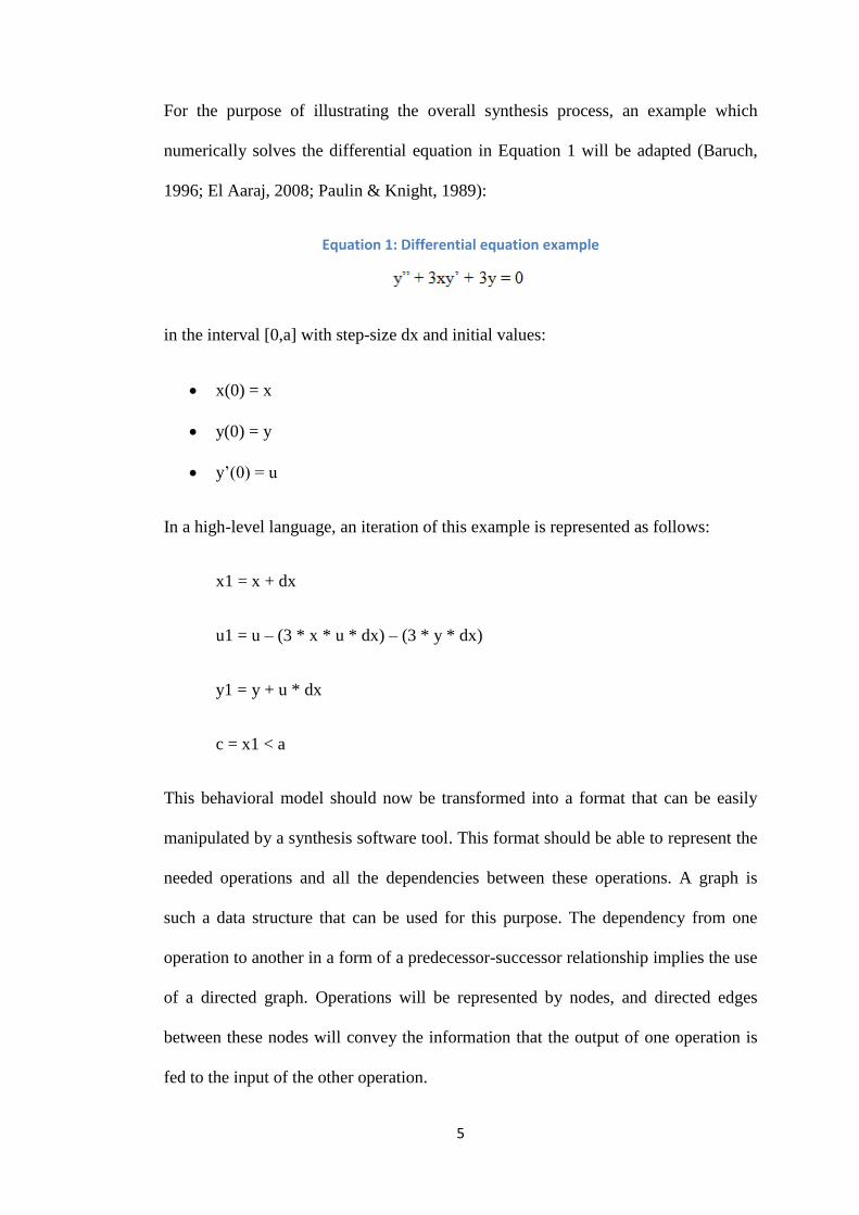
For the purpose of illustrating the overall synthesis process, an example which
numerically solves the differential equation in Equation 1 will be adapted (Baruch,
1996; El Aaraj, 2008; Paulin & Knight, 1989):
Equation 1: Differential equation example
in the interval [0,a] with step-size dx and initial values:
x(0) = x
y(0) = y
y’(0) = u
In a high-level language, an iteration of this example is represented as follows:
x1 = x + dx
u1 = u – (3 * x * u * dx) – (3 * y * dx)
y1 = y + u * dx
c = x1 < a
This behavioral model should now be transformed into a format that can be easily
manipulated by a synthesis software tool. This format should be able to represent the
needed operations and all the dependencies between these operations. A graph is
such a data structure that can be used for this purpose. The dependency from one
operation to another in a form of a predecessor-successor relationship implies the use
of a directed graph. Operations will be represented by nodes, and directed edges
between these nodes will convey the information that the output of one operation is
fed to the input of the other operation.

6
In high-level synthesis, this type of graph is known as a control data flow graph
(CDFG). The CDFG of the differential equation problem is shown in Figure 1. The
CDFG is represented by the notation G(V,E). ‘G’ represents the graph which is
constituted by a set of vertices ‘V’ connected by a set of edges ‘E’. Throughout this
work, the notion of nodes and vertices will be used interchangeably. Two “NOP”
nodes are added to the graph representing the source and the sink. These two nodes
have the lowest and highest indexes. For notation purposes, if two nodes are
connected together by an edge, the upper node will be called the predecessor of the
lower node in the graph, and the lower node will be called the successor of the upper
node. In the adopted example, as shown in Figure 1, node 2 is the predecessor of
node 3 and node 3 is the successor of node 2. A directed edge exists between those 2
vertices and thus the value produced by node 2 will be consumed by node 3. The
lifetime of the variable produced at the output of node 2 starts after node 2 and ends
right before node 3 consumes its value.

7
Figure 1: CDFG of the differential equation problem
As stated earlier, the CDFG will be the data structure used to perform the scheduling
and binding processes in high-level synthesis. These two processes are discussed in
the following sections.

8
2.1.1. Scheduling
Scheduling is an important step of high-level synthesis which should occur before
the binding process. While scheduling, the appropriate timing for each vertex in the
CDFG is determined. This means that start time of each operation and the lifetime of
every variable are set. This is performed since the CDFG only presents dependencies
in the design and does not provide any information about the time of execution of
each operation. Scheduling should always consider ensure that all the predecessor-
successor relationships that exist in the graph will remain the same. For example, in
the differential equation CDFG shown in Figure 1, if node 2 is scheduled at time 1,
then node 3 should be scheduled at a later time. If both vertices are schedules at the
same time, the predecessor-successor dependency between the two vertices will not
hold anymore. Both operations cannot run in parallel, one operation should wait until
the output of the other operation is produced and fed into it.
It can be deduced that the number of operations scheduled at the same time is in
direct relationship with the minimum number of resources needed. The fewer the
resources are, the longer the schedule will be to accommodate for the waiting time
caused by the unavailability of some resources at a certain time. One type of
scheduling, which is list scheduling, addresses this problem and will be discussed
later on. These types of algorithms are area or time constrained algorithms. They can
set area constraints by setting a limit on the number of available resources; this
reduces the number of allowed parallel operations and increases the schedule’s time.
They can also be time constrained by setting a maximum time for the schedule, while
trying to use the minimum number of resources during that time. This tradeoff
between area and delay is at the heart of high-level synthesis, and many studies have

9
been conducted in this area trying to minimize the effect of one design factor on the
other (Logesh, Harish Ram, & Bhuvaneswari, 2011a, 2011b, 2011c).
The most important scheduling algorithms are discussed next. Nevertheless, this is
not a comprehensive discussion of those algorithms which are further explained in
other sources in a more detailed fashion (Gajski et al., 1992). In the following,
scheduling algorithm will be divided into two groups, unconstrained scheduling
algorithms and constrained scheduling algorithms.
2.1.1.1. Unconstrained scheduling
Unconstrained scheduling algorithms are algorithms that schedule the CDFG while
not having any constraints on the available amount of resources. However, the
schedule should achieve minimum latency.
ASAP scheduling algorithm
ASAP, or as soon as possible, scheduling algorithm assigns each node to the earliest
time it can start. Figure 2 shows the pseudo code for this algorithm (Gajski et al.,
1992):

10
Figure 2: ASAP scheduling algorithm (Gajski et al., 1992)
In Figure 2, ‘V’ represents the set of vertices, ‘Predvi’ represents the predecessors of
the current vertex, and ‘Ei’ represents the ASAP time of the current vertex.
ALL_NODES_SCHED (Predvi, E) returns true if all predecessors of the current node
are already scheduled, and it returns false otherwise. MAX (Predvi, E) return the
maximum time of all the predecessors of the current node.
If we apply the ASAP scheduling algorithm on the differential equation example
DFG we will obtain the schedule shown in Figure 3:

11
Figure 3: ASAP scheduled differential circuit
12
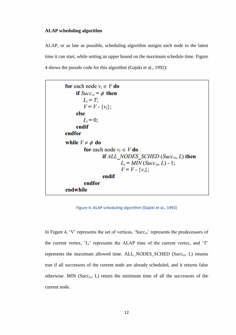
ALAP scheduling algorithm
ALAP, or as late as possible, scheduling algorithm assigns each node to the latest
time it can start, while setting an upper bound on the maximum schedule time. Figure
4 shows the pseudo code for this algorithm (Gajski et al., 1992):
Figure 4: ALAP scheduling algorithm (Gajski et al., 1992)
In Figure 4, ‘V’ represents the set of vertices, ‘Succvi’ represents the predecessors of
the current vertex, ‘Li’ represents the ALAP time of the current vertex, and ‘T’
represents the maximum allowed time. ALL_NODES_SCHED (Succvi, L) returns
true if all successors of the current node are already scheduled, and it returns false
otherwise. MIN (Succvi, L) return the minimum time of all the successors of the
current node.

13
If we apply the ALAP scheduling algorithm on the differential equation example
DFG we will obtain the schedule shown in Figure 5:
Figure 5: ALAP scheduled differential circuit

14
2.1.1.2. Constrained Scheduling
In this work, constrained scheduling was used to set bounds on the number of
available resources. Constrained scheduling algorithms use important information
obtained from the unconstrained scheduling algorithms, in order to set priorities
during the scheduling process.
Unconstrained scheduling algorithms did not set bounds on any design metric, and
ended up giving the best schedule with the minimum possible latency. But when
setting bounds on the area (i.e. the number of available resources) using constrained
scheduling algorithms, the overall delay of the circuit will tend to increase as the area
decreases.
The constrained scheduling algorithm used in this work is the list scheduling
algorithm which will be discusses in the following section.
List scheduling algorithm
List scheduling is a constrained scheduling algorithm which can be used to solve the
minimal latency resource-constrained and the minimal resource latency-constrained
problems. In this work, it is used to solve minimal latency resource-constrained
problems.
The list scheduling algorithm assigns nodes to be executed in a certain time slot only
if the available number of resources is enough. It starts scheduling nodes based on a
certain priority list which is the mobility in our case. Mobility is the difference
between the ALAP time of the node and its ASAP time. This means that the mobility

15
gives an idea about how much the node can move up and down in the schedule
without violating the predecessor-successor relationship.
The list scheduling algorithm will start first by scheduling nodes having the highest
priority then it moves to other nodes having more and more a lower priority. When
taking mobility as the priority, nodes belonging to the critical path will be those
which will be scheduled first. Figure 6 shows the effect on the latency when not
scheduling the critical path nodes first.
Figure 6: Delaying nodes on the critical path increases total latency

16
Figure 7 shows the pseudo code for this algorithm (Gajski et al., 1992):
Figure 7: List scheduling algorithm (Gajski et al., 1992)
In Figure 7, each ‘PList’ represents a priority list of nodes for each operation type
which are sorted according to their mobility. INSERT_READY_OPS scans the set of
nodes, determines if any of the operations in the set are ready, deletes each ready
node from the set V and appends it to one of the priority lists based on its operation
type. SCHEDULE_OP(Scurrent, oi, sj) returns a new schedule after scheduling the
operation oi in control step sj. The function DELETE(PListtk, oi) deletes the indicated
operation oi from the specified list.
Figure 8 shows a list scheduled graph which is constrained by the number of
available resources shown in Table 1.

17
Table 1: Available resources
Resource Type Available Quantity
Multiplier (*) 3
Adder (+) 1
Subtractor (-) 1
Less than (<) 1

18
Figure 8: List scheduled differential circuit
The next step after the scheduling process is the binding process which will be
discussed in the next section.

19
2.1.2. Binding
Binding is the process of mapping the scheduled graph to actual components. During
this process operations are mapped to certain functional units, variables are mapped
to appropriate registers, and interconnections are routed appropriately between
components.
Since the purpose of this work is not to optimize a certain partitioning heuristic or to
come up with a new one, the left-edge algorithm was used due to its simplicity and
the certainty of obtaining results in the least amount of time. This algorithm was used
for both functional units allocation and registers binding, and it will be discussed
next.
2.1.2.1. Left-Edge algorithm
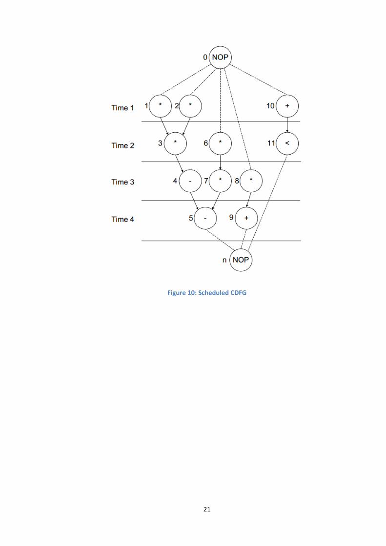
The pseudo code in Figure 9 describes the general behavior of the left-edge
algorithm which can be altered based on its application needs and priorities (De
Micheli, 1994).

20
Figure 9: Left-Edge algorithm (De Micheli, 1994)
To illustrate how the left-edge algorithm can solve the binding problem, we will use
the same differential equation circuit with a predefined schedule. This is shown in
Figure 10. The compatibility graphs for the multiplier and the ALU units of this
example are presented in Figure 11 to better understand the left-edge algorithm
functionality.
21
Figure 10: Scheduled CDFG

22
Figure 11: Multiplier and ALU compatibility graphs
Given the scheduled CDFG in Figure 10, the left-edge algorithm will allocate each
operation to its corresponding functional unit.
As a result of the algorithm we will obtain the following functional units:
A multiplier which achieves the job of node 1 from Time 1, node 3 from
Time 2, and node 7 from Time 3.
Another multiplier which achieves the job of node 2 from Time 1, node 6
from Time 2, and node 8 from Time 3.

23
An ALU which achieves the job of node 10 from Time 1, node 11 from Time
2, node 4 from Time 3, and node 5 from Time 4.
Another ALU which achieves the job of node 9 from Time 4.
2.2. Previous work
Various techniques in previous works were developed in order to minimize power
consumption in VLSI circuits. Some of these techniques will be presented in the
following:
One technique tried to save power by analyzing unnecessary switching. It
worked on reducing the spurious switching activities in a circuit by altering
register bindings in high-level synthesis using a cool-down simulated
annealing approach (El Aaraj, 2009).
Another technique minimized the power consumption by optimizing
functional unit binding. This technique focused on reducing the switching
activity of components by reducing the transition of their inputs (Bassil,
2011).
A multi-voltage technique used floorplanning to reduce power consumption.
It splits the design into voltage clusters and gets information about the
interconnections and the switching activities in order to minimize the total
power dissipation (Wei et al., 2010).
One work proposed a simultaneous functional units and register allocation
method in order to save power. This method combined heuristic list
scheduling and left-edge algorithms to optimize the number of registers and
their power (Wu et al., 2010).

24
Another developed approach focused on reducing the static power
consumption of designs under the expenditure of minimum control steps. For
this purpose, a heuristic was developed which is based on a priority indicator
and the depency matrix algorithm (Sengupta et al., 2011).
The last mentioned technique used coding methods to reduce power
consumption. It used Gray and Hybrid encoding methods for arithmetic
operators in order to reduce the switching activity (Costa et al., 2001).
This is in addition to many other multi-objective power, area and delay approaches
which tried minimizing a cost function based on these three design metrics (Logesh
et al., 2011a, 2011b, 2011c; Wu et al., 2009).
25
CHAPTER THREE
PARALLEL MULTI-VOLTAGE POWER
MINIMIZATION
This work focuses on power saving in high-level synthesis using multiple voltage
levels across the VLSI circuit components. Further improvements were made by
minimizing the runtime of the synthesis process by using parallel programming
techniques. Multi-voltage power minimization will be discussed next, followed by
the parallel approach.
3.1. Multi-voltage power minimization
Many studies in the past tried to minimize power consumption in VLSI designs, but
the techniques that yielded the best improvements were those which minimized
voltages across the chip. This fact is due to the relationship between power and
voltage shown in Equation 2 (Gerez, 1998).
Equation 2: Power consumption
Where ‘P’ is the power consumption, ‘C’ is the capacitive load, ‘V’ is the voltage,
and ‘f’ is the switching frequency. This relationship states that a certain drop in the
26
voltage level will yield a quadratic drop in power, and a raise in the voltage level will
yield a quadratic raise in power consumption.
3.1.1. Challenges
Reducing voltage levels in order to significantly minimize power consumption seems
to be an easy task if one does not observe its challenges and negative effects. The
most important challenges are discussed next.
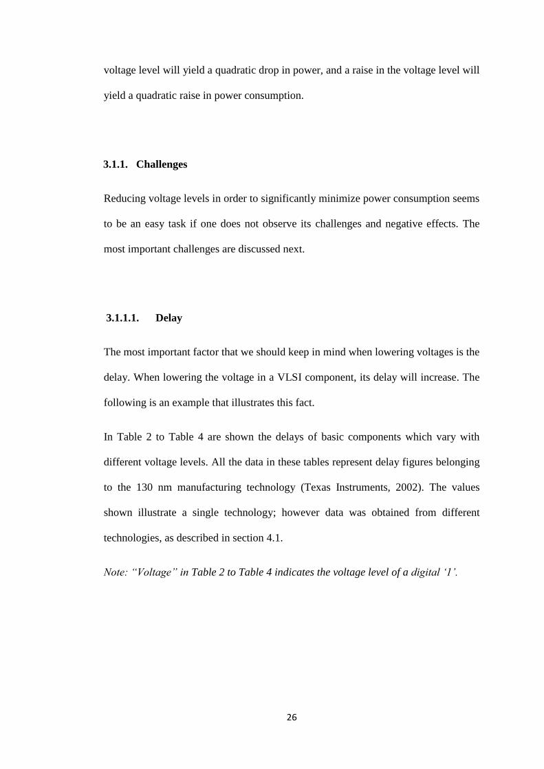
3.1.1.1. Delay
The most important factor that we should keep in mind when lowering voltages is the
delay. When lowering the voltage in a VLSI component, its delay will increase. The
following is an example that illustrates this fact.
In Table 2 to Table 4 are shown the delays of basic components which vary with
different voltage levels. All the data in these tables represent delay figures belonging
to the 130 nm manufacturing technology (Texas Instruments, 2002). The values
shown illustrate a single technology; however data was obtained from different
technologies, as described in section 4.1.
Note: “Voltage” in Table 2 to Table 4 indicates the voltage level of a digital ‘1’.

27
Table 2: 2-input AND gate delay
Voltage (V) Propagation Delay (ns)
1.8 8
2.5 5.5
3.3 4.5
5 4
Figure 12: 2-input AND gate delay vs. voltage
0
2
4
6
8
10
0 1 2 3 4 5 6
Tpd
(n
s)
Voltage (V)
2-input AND gate delay vs. voltage

28
Table 3: 2-input OR gate delay
Voltage (V) Propagation Delay (ns)
1.8 8
2.5 5.5
3.3 4.5
5 4
Figure 13: 2-input OR gate delay vs. voltage
0
2
4
6
8
10
0 1 2 3 4 5 6
Tpd
(n
s)
Voltage (V)
2-input OR gate delay vs. voltage

29
Table 4: 2-input XOR gate delay
Voltage (V) Propagation Delay (ns)
1.8 9.9
2.5 5.5
3.3 5
5 4
Figure 14: 2-input XOR gate delay vs. voltage
Based on these basic gates, if we calculate the propagation delay of the full adder of
Figure 15 we obtain the results shown in Table 5.
0
2
4
6
8
10
12
0 1 2 3 4 5 6
Tpd
(n
s)
Voltage (V)
2-input XOR gate delay vs. voltage
30
Figure 15: Full adder
Table 5: Full adder delay
Voltage (V) Propagation Delay (ns)
1.8 25.9
2.5 16.5
3.3 14
5 12

31
Figure 16: Full adder delay vs. voltage
From this example, it can be noticed that the delay increases exponentially when the
voltage level decreases.
3.1.1.2. Voltage conversion modules
When using multiple voltages in the same design, components operating at different
voltages have to be able to communicate without errors in understanding the
incoming signal. This is why we need some kind of voltage conversion modules,
which take the incoming voltage from the output of one functional unit and transform
it in order to be compatible with the input voltage of the next functional unit.
These voltage conversion modules can be classified into two types:
Modules that amplify the incoming voltage: they take as input a lower
voltage and output a higher voltage.
0
5
10
15
20
25
30
0 1 2 3 4 5 6
Tpd
(n
s)
Voltage (V)
Full adder delay vs. voltage

32
Modules that reduce the incoming voltage: they take as input a higher voltage
and output a lower voltage.
Adding these voltage conversion modules to the design will increase the design area
and introduce more delay and power consumption. This is why the modules should
be designed in order not to have a great effect on the mentioned factors; also, and
most importantly, voltages should be smartly distributed between components in
order to minimize the number of needed conversions.
3.1.1.3. Static and dynamic power consumption
There are two major sources of power consumption: static power and dynamic
power. Dynamic power consumption is due to the switching activity of internal
components, while static power, known also as leakage power, is the power
dissipated while the input is not switching (Weste & Harris, 2011).
When designing VLSI circuits, having paths from voltage sources to ground through
some components should be avoided in order not to have large static power
consumption and probably overheating the chip. This should be considered very
carefully when designing the voltage conversion modules.
3.1.1.4. Threshold voltage
Voltage levels cannot be decreased arbitrarily since each VLSI technology has its
certain limits depending on the transistor size and other factors. This constraint

33
ensures that the threshold voltage will always be able to differentiate between a
digital ‘1’ and a digital ‘0’.
This said, only tested voltage levels should be used with each technology type, while
always giving the component enough delay with the appropriate voltage in order to
ensure the proper detection of high voltages and low voltages.
3.1.2. Overcoming challenges and improving previous works
This work takes care of all the challenges that were presented in section 3.1.1, along
with the deficiencies present in previous works which were mentioned earlier. These
solutions and improvements are discussed in the coming sections.
3.1.2.1. Delay
The proposed approach takes into consideration that the delay of a design can
increase when the voltage is decreased or when extra components, such as voltage
conversion modules, are added. It solves this problem by maintaining the same
original voltage for the critical path in the design, and then it tries to reduce voltages
in components belonging to other paths. This is realized while always ensuring that
none of the non-critical paths delays exceeds the critical path delay.

34
3.1.2.2. Voltage conversion modules and static power
First, by going deeper in a lower level of abstraction, connections between transistors
are examined in order to check if both types of voltage converters mentioned earlier
are needed.
When two components operating at different voltage levels are connected, the gate of
the input transistor of the second component is fed by the output of the first one. If
this voltage at the gate is enough to form the transistor channel, then there is no need
to use voltage conversion modules.
A transistor can be in one of the following modes (Weste et al., 2011):
Off: if VGS < Vt
Saturation: if VDS > VGS - Vt
Triode: if VDS < VGS - Vt
Where “Vt” is the threshold voltage which is usually between 0.3 and 1 (normally
close to 0.3), “VGS” is the voltage between the gate and the source, and “VDS” is the
voltage between the drain and the source.
In this work, four voltage levels are used which are 5V, 3.3V, 2.5V and 1.8V. These
four voltage levels were chosen since they are used as standards in many
contemporary data books. By replacing those numbers for all combinations in the
above equations, it can be noticed that no conversion modules are needed when a
higher voltage is fed to the gate of a transistor driving a lower voltage, while
amplifiers are needed for the opposite case. By knowing that amplifiers are needed
only when a functional unit operating at a lower voltage is feeding another functional
35
unit operating at a higher voltage, the number of voltage conversion modules shrinks
significantly.
As for the amplifiers, only CMOS based amplifiers are used in order to avoid the
static power consumption problem. These amplifiers also have a very small area,
delay and power consumption compared with the design area, delay and power. The
exact effects of the amplifiers on the total area, delay, and power will be shown with
the results in the next chapter. It is worthwhile to note that, according to what was
mentioned earlier in the previous section, the original delay, which is the critical path
delay, will not increase at all even with the presence of those amplifiers since the
critical path will not be altered.
Several amplifier designs were considered in this work: the direct compensation
amplifier, the indirect compensation amplifier, the differential amplifier and the
push-pull common source amplifier (Allen & Holberg, 2011; Baker, 2013). Layouts
of these designs are shown in Figure 17 to Figure 20.

36
Figure 17: Direct compensation amplifier (Baker, 2013)
Figure 18: Indirect compensation amplifier (Baker, 2013)

37
Figure 19: Differential amplifier (Allen et al., 2011)
Figure 20: Push-pull common source amplifier (Allen et al., 2011)

38
3.1.2.3. Threshold voltage
To ensure the proper detection of high voltage levels and low voltage levels, and to
ensure that all the results are accurate and practical, all voltages used in this work
along with the corresponding delay of each component are extracted from data books
belonging to different technologies, as described in section 4.1.
3.1.2.4. Optimizing in high-level synthesis
Instead of optimizing at lower levels of abstraction, this work focuses on optimizing
power consumption at high-level synthesis, which can yield more power saving.
Table 6 shows how the opportunities for power saving in higher levels of synthesis
are much greater than working at the lower levels.
Table 6: Opportunities for power saving (Pedram, 1999)
Synthesis Level Opportunities for power saving
System > 70%
Behavioral 40-70%
RT-level 25-40%
Logic 15-25%
Physical 10-15%
3.1.3. Power minimization approach
The main idea behind the power minimization approach is to save power while
ensuring that the delay is not increased.

39
3.1.3.1. Designs without reuse
For designs without component reuse, the algorithm starts by scheduling nodes based
on ASAP scheduling algorithm. The maximum time, calculated in clock cycles, is
taken from the ASAP schedule and is given as parameter to the ALAP scheduling
algorithm. Once we have both ASAP and ALAP times for each node, four voltage
levels are assigned to the nodes according to their mobility. These four voltages are
5V, 3.3V, 2.5V and 1.8V. So the nodes are divided into four groups according to
their mobility; the group having the least mobility is assigned the highest voltage
while the group with the highest mobility is assigned the lowest voltage. This is done
in order to start with an initial solution that takes the delay into consideration. After
assigning initial voltages, voltage amplifiers are inserted where needed in the design.
Then each path is visited in order to see whether its total delay exceeds the critical
path delay or not. If it does, the node having the lowest voltage in the corresponding
path is assigned a higher voltage, and the process is repeated until all paths have
delays which do not exceed the critical path delay. At the end, the new total power
consumption is calculated and compared with the total power consumption of the
same design while having all functional units working at 5V. Figure 21 shows the
pseudo code of the algorithm. Note that α, β and γ are parameters corresponding to
values between 0 and 1. These parameters divide the critical path total time into 4
parts:
Part 1: from 0 to α*critical_path_time
Part 2: from α*critical_path_time to β*critical_path_time
Part 3: from β*critical_path_time to γ*critical_path_time
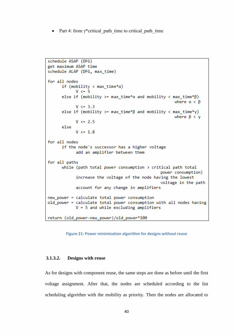
40
Part 4: from γ*critical_path_time to critical_path_time
Figure 21: Power minimization algorithm for designs without reuse
3.1.3.2. Designs with reuse
As for designs with component reuse, the same steps are done as before until the first
voltage assignment. After that, the nodes are scheduled according to the list
scheduling algorithm with the mobility as priority. Then the nodes are allocated to

41
their corresponding functional units, and registers and multiplexers are added
accordingly. Each functional unit is assigned the highest voltage of its nodes and
amplifiers are inserted where needed. Paths are visited in the same manner as before
to ensure that each path’s delay does not exceed the critical path delay. At the end,
the new total power consumption is calculated and compared with the total power
consumption of the same design while having all functional units working at 5V.
Figure 22 shows the pseudo code of the algorithm. (note that the choice of α, β and γ
parameters is discussed later on)

42
Figure 22: Power minimization algorithm for designs with reuse

43
3.1.3.3. Optimizing the algorithm
The algorithms discussed earlier were studied thoroughly and many improvements
were implemented in order to further improve power saving. The main optimizations
that were added to the original algorithm are the following:
Changing α, β, and γ parameters: these three parameters had a major effect on
the solution. When these parameters have small values, the power
consumption improvement tends to be little. As these parameter get higher
values, the power consumption improvement gets higher until reaching a
certain maximum for each design. Keeping in mind that these three
parameters cannot be always set to a certain minimum since runtime will rise
with their increase. This is due to the fact that lower voltages will be assigned
to components, thus more iterations will be needed in order to lower the delay
of each path by increasing voltages.
Scheduling moves: in designs with reuse, there is a large number of solutions
when allocating functional units. These solutions are explored by exploring
many schedules for the same design before allocation is done. To do so, at
each iteration, a random node that has non-zero mobility is selected and is
moved one step randomly in the schedule. Then the allocation is done and
power improvement is calculated. These iterations are repeated until the
power improvement converges to its optimal value.
Changing resource bags: the number of available components of each type
was also changed in a certain interval and different results were obtained.
Changing allocation combinations: when allocating at a certain control step,
there are several options to choose from. This choice has its effects on the

44
final design. Thus, all allocation options for each schedule were also tried and
the one yielding the best results was chosen.
Changing the order of traversal: the order of traversal of a certain design
when allocating also has some effects on the results. For this purpose, each
allocation was tried twice, once beginning from the first node in the list and
another time beginning from the last node. The allocation which yielded the
best result was selected.

45
3.2. Parallel multi-voltage power minimization
Parallel programming techniques can always be used in order to improve runtime in
a certain algorithm where there are tasks that can be realized independently. In this
work, parallel programming was used to implement the part which was responsible
for the schedule moves in designs with reuse.
As stated earlier, schedule moves were done randomly to random nodes, and these
iterations keep running until converging and obtaining the optimal result. This
process was parallelized by implementing the algorithm shown in Figure 23.
Figure 23: The parallel algorithm
As shown in Figure 23, the parallelism is exploited taking the compute-intensive
tasks in the developed approach and executing them in parallel. These tasks are the
repeated move-and-allocate tasks which take the largest portion of the execution
time. If these tasks were to be executed serially, the runtime will increase
exponentially with the increase of the number of nodes in the design.

46
When running this algorithm on an n-thread machine, the first thread will always be
in charge of the serial tasks which precede and follow the parallel section of the
algorithm; and it also participates, as all the other n-1 threads, in the parallel part of
the algorithm. The data communication between threads is kept to a minimum; it
consists of the following:
When forking to its children, the parent thread (first thread) will send a
scheduled graph to all other threads. This scheduled graph consists of an
array containing all nodes of the DFG, each having its ASAP time and ALAP
time. Therefore the size of this communicated data increases proportionally to
the number of nodes in the DFG.
When all threads synchronize and report their results back to the parent
thread, only the power savings value obtained by each thread is sent back to
the parent.

47
CHAPTER FOUR
EXPERIMENTAL RESULTS
The developed approaches were tested on the implemented synthesis software suite
on 7 different benchmarks and yielded the following average results:
Power consumption minimization for designs without reuse: 36.57%
Power consumption minimization for designs with reuse: 33.30%
Average thread utilization after introducing parallel programming on an 8-
thread machine: 66.12%
In the following, the technology metrics that were used will be presented. After that,
the used benchmarks will be illustrated along with all obtained results for different
simulations.
4.1. Technology metrics
After trying different values belonging to data books from different technologies and
manufacturers, it was noticed that the overall results for each technology were nearly
the same. For this reason, values used for power, area and delay were averages of the
values obtained from different data books belonging to different technologies shown
in Table 7 (ALLDATASHEET.COM, 2013; DatasheetCatalog.com, 2013; ON
Semiconductor, 2000; Texas Instruments, 2002).

48
Table 7: Technologies used
Manufacturer Feature Size (nm)
ON Semiconductor 180
Texas Instruments 130
Motorola 90
Fairchild Semiconductor 34
National Semiconductor 22
4.2. Benchmarks
A total of 7 benchmarks were used. They are presented in the following in an
ascending order according to the number of nodes in each benchmark (ExPRESS
Group, 2005).

49
4.2.1. HAL:
Figure 24: HAL benchmark DFG
Total number of nodes: 11
Total number of edges: 8
Average edges per node: 0.72
Critical path delay: 4
Parallelism (nodes / critical path): 2.75

50
4.2.2. ARF:
Figure 25: ARF benchmark DFG
Total number of nodes: 28
Total number of edges: 30
Average edges per node: 1.07
Critical path delay: 8
Parallelism (nodes / critical path): 3.5

51
4.2.3. EWF:
Figure 26: EWF benchmark DFG

52
Total number of nodes: 34
Total number of edges: 47
Average edges per node: 1.38
Critical path delay: 14
Parallelism (nodes / critical path): 2.42

53
4.2.4. FIR1:
Figure 27: FIR1 benchmark DFG

54
Total number of nodes: 40
Total number of edges: 39
Average edges per node: 0.97
Critical path delay: 11
Parallelism (nodes / critical path): 3.63

55
4.2.5. FIR:
Figure 28: FIR benchmark DFG
Total number of nodes: 44
Total number of edges: 43
Average edges per node: 0.97
Critical path delay: 11
Parallelism (nodes / critical path): 4

56
4.2.6. COS1:
Figure 29: COS1 benchmark DFG
Total number of nodes: 66
Total number of edges: 76
Average edges per node: 1.15
Critical path delay: 8
Parallelism (nodes / critical path): 8.25

57
4.2.7. COS2:
Figure 30: COS2 benchmark DFG
Total number of nodes: 92
Total number of edges: 91
Average edges per node: 0.98
Critical path delay: 8
Parallelism (nodes / critical path): 11.5

58
4.3. Results and analysis
4.3.1. Power saving results for designs without reuse
The results in Table 8 show the power savings for each benchmark, without
component reuse, for optimal values of α, β and γ parameters.
Table 8: Power savings for designs without reuse (optimal α, β and γ parameters)
Benchmark Power savings (%)
HAL 35.58
ARF 20.34
EWF 26.16
FIR1 52.44
FIR 57.15
COS1 26.41
COS2 37.91
Average 36.57
Maximum 57.15
Minimum 20.34
It can be noticed that the higher power saving values correspond to the benchmarks
having the smallest average edges per node value. This is due to the fact that
decreasing the number of average edges per node gives the design greater mobility
values. Having greater mobility will enable nodes to be assigned lower voltages,
which means consuming less power. Note that the optimal values of α, β and γ

59
parameters are benchmark-specific and vary from one benchmark to another.
Furthermore, after experimentation, no correlation was found between the
benchmarks’ specifications and the optimal values of α, β and γ; these parameters
can only be obtained through experimentation.
In the following, the power saving results are presented for each benchmark for other
values of α, β and γ parameters will be presented. The starting point of the simulation
was always at α, β and γ values of 25%, 50% and 75% respectively (those values
divide the critical path time into four equal portions). Starting from this initial
partitioning, these parameters were decreased until reaching maximum power
savings.

60
4.3.1.1. HAL:
Figure 31: HAL power savings for different α, β and γ parameters (no reuse)
0.00
5.00
10.00
15.00
20.00
25.00
30.00
35.00
40.00
25, 50, 75 20, 50, 75 16, 50, 75 16, 33, 75 16, 33, 50 14, 25, 33 10, 16, 24 6, 10, 20
Po
we
r sa
vin
gs (
%)
α, β, γ parameters (%)
HAL power savings for different α, β and γ parameters (no reuse)
61
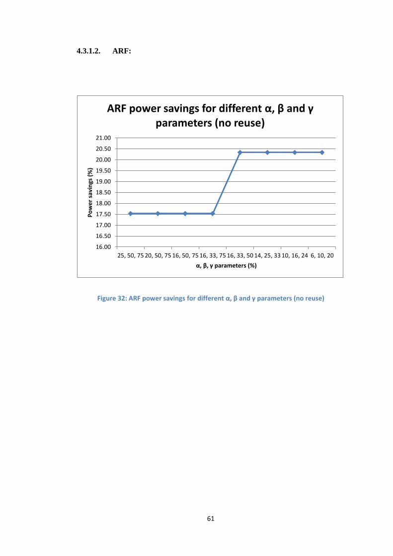
4.3.1.2. ARF:
Figure 32: ARF power savings for different α, β and γ parameters (no reuse)
16.00
16.50
17.00
17.50
18.00
18.50
19.00
19.50
20.00
20.50
21.00
25, 50, 75 20, 50, 75 16, 50, 75 16, 33, 75 16, 33, 50 14, 25, 33 10, 16, 24 6, 10, 20
Po
we
r sa
vin
gs (
%)
α, β, γ parameters (%)
ARF power savings for different α, β and γ parameters (no reuse)

62
4.3.1.3. EWF:
Figure 33: EWF power savings for different α, β and γ parameters (no reuse)
0.00
5.00
10.00
15.00
20.00
25.00
30.00
25, 50, 75 16, 25, 50 10, 20, 33 6, 10, 20 6, 8, 12 5, 6, 10 5, 5.5, 6 4, 5, 6
Po
we
r sa
vin
gs (
%)
α, β, γ parameters (%)
EWF power savings for different α, β and γ parameters (no reuse)

63
4.3.1.4. FIR1:
Figure 34: FIR1 power savings for different α, β and γ parameters (no reuse)
0.00
10.00
20.00
30.00
40.00
50.00
60.00
25, 50,75
20, 50,75
20, 33,75
16, 33,75
16, 33,50
12, 25,50
10, 20,33
6, 10,16
5, 6, 10 4, 5, 6
Po
we
r sa
vin
gs (
%)
α, β, γ parameters (%)
FIR1 power savings for different α, β and γ parameters (no reuse)

64
4.3.1.5. FIR:
Figure 35: FIR power savings for different α, β and γ parameters (no reuse)
0.00
10.00
20.00
30.00
40.00
50.00
60.00
70.00
25, 50,75
20, 50,75
20, 33,75
16, 33,75
16, 25,75
16, 25,50
12, 20,50
10, 16,33
6, 10,20
5, 6, 10
Po
we
r sa
vin
gs (
%)
α, β, γ parameters (%)
FIR power savings for different α, β and γ parameters (no reuse)

65
4.3.1.6. COS1:
Figure 36: COS1 power savings for different α, β and γ parameters (no reuse)
0.00
5.00
10.00
15.00
20.00
25.00
30.00
25, 50, 75 20, 50, 75 20, 33, 75 16, 33, 75 16, 33, 50 5, 6, 10
Po
we
r sa
vin
gs (
%)
α, β, γ parameters (%)
COS1 power savings for different α, β and γ parameters (no reuse)

66
4.3.1.7. COS2:
Figure 37: COS2 power savings for different α, β and γ parameters (no reuse)
0.00
5.00
10.00
15.00
20.00
25.00
30.00
35.00
40.00
25, 50,75
20, 33,75
16, 33,75
16, 25,75
16, 25,50
12, 25,50
12, 20,33
10, 16,33
10, 12,33
6, 10,16
Po
we
r sa
vin
gs (
%)
α, β, γ parameters (%)
COS2 power savings for different α, β and γ parameters (no reuse)

67
The results of Figure 31 to Figure 37 obtained in the 7 benchmarks clearly show how
power consumption is further minimized with the decrease of α, β and γ parameters.
This is because when decreasing these parameters more parts will be assigned a
lower voltage in the initial solution. The result of each benchmark, as shown, has a
certain limit which is at the minimum power consumption for this benchmark. When
assigning values to α, β and γ which are smaller, no improvements will occur, but the
runtime will increase since the iterations will increase in order to fix the delays of
non-critical paths and raise their voltages. Note that, in COS1 benchmark, optimal
values of α, β and γ were reached from the first iteration; thus the graph of Figure 36
does not show further improvement.

68
4.3.2. Power saving results for designs with reuse
In Table 9 to Table 23, power saving results for all benchmarks with component
reuse are presented for different resource bags.
Note that the results shown are for optimal values of α, β and γ obtained for non-
reuse cases, though it is not guaranteed that these values are the same for reuse cases
given different resource bags. Finding the optimal values of α, β and γ for each
resource bag was not tried in this study.
Table 9: Power savings for designs with reuse and unlimited resources
Benchmark Power Savings (%)
HAL 36.47
ARF 42.35
FIR1 61.50
FIR 65.58
EWF 9.65
COS1 10.75
COS2 6.82
Average 33.30
Maximum 65.58
Minimum 6.82
It can be noticed that the greatest power savings were obtained in the benchmarks
which have critical paths that do not contain many types of operations. During
allocation, when the critical path contains many types of operations, many functional

69
units of different types will be assigned operations belonging to the critical path. This
will yield having less power savings since these functional units will be assigned the
highest voltage which is 5V.

70
4.3.2.1. HAL
Table 10: Modifying the available number of multipliers while other resources are unlimited (HAL)
Number of Available Multipliers Power Savings (%)
8 36.47
7 36.47
6 36.47
5 36.47
4 24.70
3 16.50
2 20.81
Table 11: Modifying the available number of adders while other resources are unlimited (HAL)
Number of Available Adders Power Savings (%)
8 36.47
7 36.47
6 36.47
5 36.47
4 36.47
3 36.47
2 36.47
It can be noticed that when modifying the number of available adders the results do
not change. This is due to the fact that HAL benchmark has only two adders which

71
are scheduled at different clock cycles, and therefore they will be assigned to one
functional unit during the binding process. This fact does not apply when modifying
the number of available multipliers since HAL has many multipliers which are
scheduled at the same clock cycle.
72
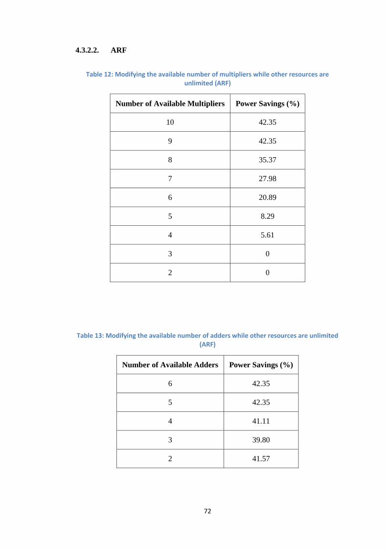
4.3.2.2. ARF
Table 12: Modifying the available number of multipliers while other resources are unlimited (ARF)
Number of Available Multipliers Power Savings (%)
10 42.35
9 42.35
8 35.37
7 27.98
6 20.89
5 8.29
4 5.61
3 0
2 0
Table 13: Modifying the available number of adders while other resources are unlimited (ARF)
Number of Available Adders Power Savings (%)
6 42.35
5 42.35
4 41.11
3 39.80
2 41.57
73
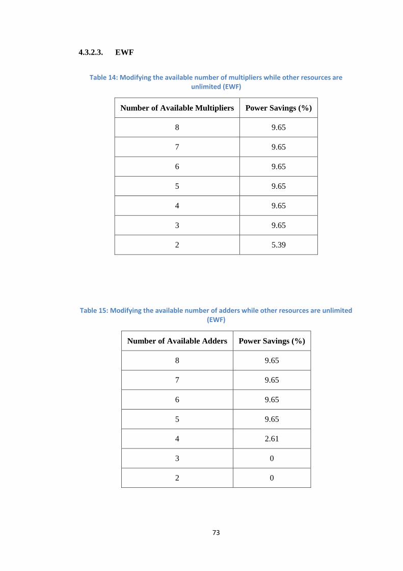
4.3.2.3. EWF
Table 14: Modifying the available number of multipliers while other resources are unlimited (EWF)
Number of Available Multipliers Power Savings (%)
8 9.65
7 9.65
6 9.65
5 9.65
4 9.65
3 9.65
2 5.39
Table 15: Modifying the available number of adders while other resources are unlimited (EWF)
Number of Available Adders Power Savings (%)
8 9.65
7 9.65
6 9.65
5 9.65
4 2.61
3 0
2 0

74
4.3.2.4. FIR1
Table 16: Modifying the available number of multipliers while other resources are unlimited (FIR1)
Number of Available Multipliers Power Savings (%)
10 61.50
9 61.50
8 58.70
7 55.22
6 50.75
5 44.83
4 38.94
3 30.19
2 39.86
Table 17: Modifying the available number of adders while other resources are unlimited (FIR1)
Number of Available Adders Power Savings (%)
9 61.50
8 57.91
7 53.13
6 46.48
5 36.59
4 24.20
3 0
2 0

75
4.3.2.5. FIR
Table 18: Modifying the available number of multipliers while other resources are unlimited (FIR)
Number of Available Multipliers Power Savings (%)
13 65.58
12 65.58
11 63.60
10 61.23
9 58.32
8 53.62
7 48.57
6 43.87
5 39.70
4 26.70
3 0
2 0
Table 19: Modifying the available number of adders while other resources are unlimited (FIR)
Number of Available Adders Power Savings (%)
4 65.58
3 65.12
2 64.63

76
It can be noticed that in HAL and FIR benchmarks, when dropping down the
available number of multipliers, the power savings decrease until reaching 0. This
means that, when decreasing the number of available multipliers, the multipliers’
functional units are assigned more and more operations belonging to the critical path,
while all other functional units already contain critical path operations. This process
continues until all functional units contain operations belonging to the critical path;
therefore they will all be assigned the highest voltage level and there will be no
power saving.
The same can be noticed here as for ARF, EWF and FIR1 benchmark, but it is
happening for adders rather than multipliers.

77
4.3.2.6. COS1
Table 20: Modifying the available number of multipliers while other resources are unlimited (COS1)
Number of Available Multipliers Power Savings (%)
10 10.75
9 10.75
8 5.94
7 7.46
6 7.78
5 9.03
4 11.80
3 14.93
2 19.53
Table 21: Modifying the available number of adders while other resources are unlimited (COS1)
Number of Available Adders Power Savings (%)
6 10.75
5 10.75
4 9.64
3 8.46
2 11.29

78
4.3.2.7. COS2
Table 22: Modifying the available number of multipliers while other resources are unlimited (COS2)
Number of Available Multipliers Power Savings (%)
8 6.82
7 6.82
6 9.04
5 11.98
4 10.98
3 14.07
2 21.86
Table 23: Modifying the available number of adders while other resources are unlimited (COS2)
Number of Available Adders Power Savings (%)
8 6.82
7 6.82
6 6.82
5 6.82
4 6.82
3 4.69
2 8.32

79
It can be noticed from COS1 and COS2 benchmarks that, when dropping down the
available number of multipliers or adders, the power savings decrease, then they
increase until reaching values which are greater than those with infinite number of
available resources. This means that, with few resources, operations belonging to the
critical path will be assigned to functional units already containing critical path
operations, while more functional units will be assigned non-critical path operations.

80
4.3.3. Effects of amplifiers on the area
The results in Table 24 show the effect of the added amplifier on the total area of the
design.
Table 24: The effects of the added amplifiers on the total design area
Benchmark Total amplifiers area / Total design area without amplifiers
(%)
HAL 0.35
ARF 0.28
EWF 0.08
FIR1 1.35
FIR 0.89
COS1 0.11
COS2 0.29
Average 0.48
Maximum 1.35
Minimum 0.08
Table 24 clearly shows that the effects on the total design area of the added voltage
amplifiers are very negligible. This is due to the fact that the number of added
amplifiers is very small, and the design of each amplifier has a significantly small
area compared to other components.

81
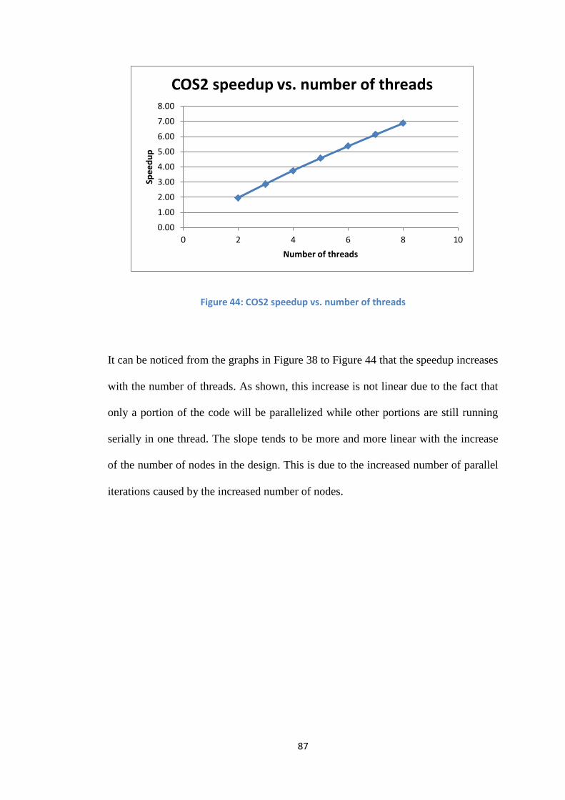
4.3.4. Speedup results
Simulations for parallel execution were performed on a platform consisting of an
Intel i7 CPU having 4 cores which support hyper-threading (8 threads), and 4GB of
RAM.
Due to the use of parallel programming techniques in designs with reuse, the runtime
has significantly decreased. Table 25 to Table 27 show the speedup gained from
exploiting parallelism for 2, 4 and 8 threads respectively, although simulations were
done for other number of threads as seen in Figure 38 to Figure 44.
Table 25: Speedup with 2 threads
Benchmark Serial Time (ns) Time with 2 threads (ns) Speedup
HAL 132.00 77.00 1.71
ARF 402.00 220.00 1.83
EWF 559.00 304.00 1.84
FIR1 400.00 220.00 1.82
FIR 473.00 253.00 1.87
COS1 1498.00 772.00 1.94
COS2 1884.00 964.00 1.95
Average 764.00 401.43 1.85
Maximum 1884.00 964.00 1.95
Minimum 132.00 77.00 1.71

82
Table 26: Speedup with 4 threads
Benchmark Serial Time (ns) Time with 4 threads (ns) Speedup
HAL 132.00 49.50 2.67
ARF 402.00 129.00 3.12
EWF 559.00 176.50 3.17
FIR1 400.00 130.00 3.08
FIR 473.00 143.00 3.31
COS1 1498.00 409.00 3.66
COS2 1884.00 504.00 3.74
Average 764.00 220.14 3.25
Maximum 1884.00 504.00 3.74
Minimum 132.00 49.50 2.67

83
Table 27: Speedup with 8 threads
Benchmark Serial Time (ns) Time with 8 threads (ns) Speedup
HAL 132.00 35.75 3.69
ARF 402.00 83.50 4.81
EWF 559.00 112.75 4.96
FIR1 400.00 85.00 4.71
FIR 473.00 88.00 5.38
COS1 1498.00 227.50 6.58
COS2 1884.00 274.00 6.88
Average 764.00 129.50 5.29
Maximum 1884.00 274.00 6.88
Minimum 132.00 35.75 3.69
It can be noticed from Table 25 to Table 27 that we always have speedup when
parallelizing. The speedup tends to increase with the number of nodes in the design.
This is expected since with more nodes, a higher number of iterations will be needed
to converge, and these iterations will be running in parallel when using parallel
programming. As can be seen in Table 27, when using 8 threads, thread utilization is
on average 66.12% (5.29 / 8) and goes up to 86% (6.88 / 8).

84
Figure 38: HAL speedup vs. number of threads
Figure 39: ARF speedup vs. number of threads
0.00
0.50
1.00
1.50
2.00
2.50
3.00
3.50
4.00
0 2 4 6 8 10
Spe
ed
up
Number of threads
HAL speedup vs. number of threads
0.00
1.00
2.00
3.00
4.00
5.00
6.00
0 2 4 6 8 10
Spe
ed
up
Number of threads
ARF speedup vs. number of threads

85
Figure 40: FIR1 speedup vs. number of threads
Figure 41: FIR speedup vs. number of threads
0.00
0.50
1.00
1.50
2.00
2.50
3.00
3.50
4.00
4.50
5.00
0 2 4 6 8 10
Spe
ed
up
Number of threads
FIR1 speedup vs. number of threads
0.00
1.00
2.00
3.00
4.00
5.00
6.00
0 2 4 6 8 10
Spe
ed
up
Number of threads
FIR speedup vs. number of threads

86
Figure 42: EWF speedup vs. number of threads
Figure 43: COS1 speedup vs. number of threads
0.00
1.00
2.00
3.00
4.00
5.00
6.00
0 2 4 6 8 10
Spe
ed
up
Number of threads
EWF speedup vs. number of threads
0.00
1.00
2.00
3.00
4.00
5.00
6.00
7.00
0 2 4 6 8 10
Spe
ed
up
NUmber of threads
COS1 speedup vs. number of threads
87
Figure 44: COS2 speedup vs. number of threads
It can be noticed from the graphs in Figure 38 to Figure 44 that the speedup increases
with the number of threads. As shown, this increase is not linear due to the fact that
only a portion of the code will be parallelized while other portions are still running
serially in one thread. The slope tends to be more and more linear with the increase
of the number of nodes in the design. This is due to the increased number of parallel
iterations caused by the increased number of nodes.
0.00
1.00
2.00
3.00
4.00
5.00
6.00
7.00
8.00
0 2 4 6 8 10
Spe
ed
up
Number of threads
COS2 speedup vs. number of threads

88
Figure 45: Average thread utilization vs. number of threads
As shown in Figure 45, the average thread utilization is dropping with the increase of
the number of threads. This is due to the fact that the parent thread will still have to
synchronize while all other threads are on hold, and this cannot be reduced. This
trend is consistent with Amdahl’s law (Hennessy & Patterson, 2012). This small
sample shows that thread utilization is dropping at a relatively low rate, which
indicates that having a higher degree of parallelism might further reduce execution
times.
Note that the parallelism parameter as stated for each benchmark was neither
correlated to the obtained power savings nor to the gained speedup.
0.00
20.00
40.00
60.00
80.00
100.00
2 3 4 5 6 7 8
Ave
rage
th
read
uti
lizat
ion
Number of threads
Average thread utilization vs. number of threads

89
CHAPTER FIVE
CONCLUSIONS AND FUTURE WORK
In this work, a new approach was developed to reduce power consumption in high-
level synthesis using multiple voltage levels. For this purpose, some deficiencies of
previous works were observed and solved in order to obtain a design that consumes
significantly less power while always having the same delay. The results obtained
concerning power consumption minimization were also better than the results of
previous works even with the introduction of voltage amplifiers. The results were
obtained after testing on seven different benchmarks and varying almost all
parameters that could be changed in order to obtain better results. Power
consumption was reduced on average by 36.57% for designs without component
reuse, and it was reduced on average by 33.3% for designs with component reuse.
Also, parallelism in the developed algorithms was exploited and the code sections
that can run independently were parallelized. The thread utilization on an 8-thread
machine averaged 66.12%.
For future work, optimal values for α, β and γ parameters can be found for different
resource bags in order to further save power. Other amplifiers’ designs can be also
tested to try to further decrease the area and static power consumption. As for
parallelism, the synthesis process could be implemented in other languages on

90
supercomputers in order to reduce the runtime much further, especially for designs
having a large number of nodes.

91
BIBLIOGRAPHY
Ahuja, S., Mathaikutty, D., Singh, G., Stetzer, J., Shukla, S., & Dingankar, A.
(2009). Power estimation methodology for a High-Level Synthesis
framework. Proceedings of the 2009 Quality of Electronic Design. Doi:
10.1109/ISQED.2009.4810352
ALLDATASHEET.COM (2013). ALLDATASHEET.COM - Datasheet search site
for electronic components and semiconductors and other semiconductors.
Retrieved from http://www.alldatasheet.com/
Allen, P., & Holberg, D. (2011). CMOS analog circuit design (3rd
ed.). Oxford:
Oxford University Press, Incorporated.
Baker, J. (2013). High speed op-amp design: Compensation and topologies for two
and three stage designs. Proceedings of the 2013 IEEE CTS CAS/SSC Jan
Meeting.
Baruch, Z. (1995). Datapath allocation. ACAM Scientific Journal, 4(2), 67-75.
Baruch, Z. (1996). Scheduling algorithms for High-Level Synthesis. ACAM Scientific
Journal, 5, 48-57.
Bassil, L. (2011). Power and temperature aware functional unit binding in High
Level Synthesis (Unpublished master’s thesis). Lebanese American
University, Lebanon.
Cherroun, H., & Feautrier, P. (2007). An exact resource constrained-scheduler using
graph coloring technique. Proceedings of the 2007 IEEE/ACS International
Conference on Computer Systems and Applications. Doi:
10.1109/AICCSA.2007.370936
Costa, E., Bampi, S., & Monteiro, J. (2001). Power optimization using coding
methods on arithmetic operators. Proceedings of the 2001 IEEE International
Symposium on Signals and Systems. Doi: 10.1.1.1.2806
Coussy, P., & Morawiec, A. (2008). High-Level Synthesis. New York: Springer
Science+Business Media, LLC.
Crosthwaite, P., Williams, J., & Sutton, P. (2009). Profile driven data-dependency
analysis for improved high level language hardware synthesis. Proceedings of
the 2009 IEEE International Conference on Field-Programmable
Technology. Doi: 10.1109/FPT.2009.5377672
92
DatasheetCatalog.com (2013). Datasheet catalog for integrated circuits, diodes,
triacs, and other semiconductors. Retrieved from
http://www.datasheetcatalog.com/
De Micheli, G. (1994). Synthesis and optimization of digital circuits. New York:
McGraw-Hill.
El Aaraj, E. (2008). A novel approach to reduce spurious switching activity in High-
Level Synthesis (Unpublished master’s thesis). Lebanese American
University, Lebanon.
ExPRESS Group (2005). ExPRESS - Benchmarks. Retrieved from
http://express.ece.ucsb.edu/benchmark/
Gajski, D., Dutt, N., Wu, A., & Lin, S. (1992). High-Level Synthesis. Boston: Kluwer
Academic Publishers.
Gerez, S. (1998). Algorithms for VLSI design automation. Chichester: John Wiley
and Sons.
Goel, N., & Singh, S. (2012). Comparative analysis of 4-bit multipliers using low
power adder cells. International Journal of Engineering Research and
Applications, 2(2), 1488-1491.
Harish Ram, D., Bhuvaneswari, M., & Logesh, S. (2011). A novel evolutionary
technique for multi-objective power, area and delay optimization in High
Level Synthesis of datapaths. Proceedings of the 2011 IEEE Computer
Society Annual Symposium on VLSI. Doi: 10.1109/ISVLSI.2011.55
Hennessy, J., & Patterson, D. (2012). Computer architecture: A quantitave approach
(5th
ed.). Waltham MA: Elsevier.
Logesh, S., Harish Ram, D., & Bhuvaneswari, M. (2011). A survey of High-Level
Synthesis techniques for area, delay and power optimization. International
Journal of Computer Applications, 32(10), 3935-3952.
Logesh, S., Harish Ram, D., & Bhuvaneswari, M. (2011). Multi-objective
optimization of power, area and delay during High-Level Synthesis of DFG’s
- a genetic algorithm approach. Proceedings of the 2011 IEEE 3rd
International Conference on Electronics Computer Technology. Doi:
10.1109/ICECTECH.2011.5941570
Mohanty, S., Ranganathan, N., Kougianos, E., & Patra, P. (2008). Low-power High-
Level Synthesis for nanoscale CMOS circuits. New York: Springer
Science+Business Media, LLC.
ON Semiconductor (2000). LS TTL date. Denver: Semiconductor Components
Industries, LLC.

93
Paulin, P., & Knight, J. (1989). Force directed scheduling for the behavioral
synthesis of ASIC’s. Computer-Aided Design of Integrated Circuits and
System IEEE Transactions on CAD/ICAS, 8(6), 661-679.
Pedram, M. (1999). Low power design methodologies and techniques: An overview.
University of Southern California. Retrieved from
http://atrak.usc.edu/~massoud/Papers/LPD-talk.pdf
Sengupta, A., Sedaghat, R., Sarkar, P., & Sehgal, S. (2011). Priority function based
power efficient rapid design space exploration of scheduling and module
selection in High Level Synthesis. Proceedings of the 2011 IEEE Canadian
Conference on Electrical and Computer Engineering. Doi:
10.1109/CCECE.2011.6030509
Texas Instruments (2002). Digital logic pocket data book. Dallas: Texas Instruments
Incorporated.
Wei, C., Li, G., & Zhang, X. (2010). Low power design method in High Level
Synthesis with multiple voltages. Proceedings of the 2010 5th IEEE
Conference on Industrial Electronics and Applicationsis. Doi:
10.1109/ICIEA.2010.5514933
Weste, N., & Harris, D. (2011). CMOS VLSI design (4th
ed.). Boston: Pearson
Education, Inc.
Wu, F., Xu, N., Yu, J., Zheng, F., & Bian, J. (2009). Exploiting power-area tradeoffs
in High-Level Synthesis through dynamic functional unit allocation.
Proceedings of the 2009 IEEE International Conference on Communications,
Circuits and Systems. Doi: 10.1109/ICCCAS.2009.5250345
Wu, F., Xu, N., Zheng, F., & Mao, F. (2010). Simultaneous functional units and
register allocation based power management for High-level Synthesis of data-
intensive applications. Proceedings of the 2010 IEEE International
Conference on Communications, Circuits and Systems. Doi:
10.1109/ICCCAS.2010.5581860

94
APPENDIX I
THE SYNTHESIS SOFTWARE SUITE
The synthesis software suite built to test this work is implemented using Java. It is
constituted of 9 classes containing a total of around 2000 lines of code. The synthesis
software takes netlists for benchmarks written in a behavioral level language as
input, parses them to create their DFGs, schedules the graph according to the desired
scheduling algorithm, and finally allocates, serially and in parallel, functional units,
registers and interconnections. During this process, the software can also calculate
any needed power, delay and area values in order to get any needed results.
Note that all power, delay and area values are based on actual data books for basic
components.
In the following, samples of the developed java code, input netlists and output are
presented.
Code sample: Scheduling class
import java.util.ArrayList; public class Scheduling { public static ArrayList<Node> asap(ArrayList<Node> n) {//ASAP scheduling algorithm int l = n.size(); Node temp; for(int i=0;i<l;i++)

95
{ temp = n.get(i); if(temp.predecessors.size()==0 || temp.predecessors.get(0).getId()==-1) { temp.setAsapTime(1); n.set(i,temp); } } //copy n to v ArrayList<Node> v = new ArrayList<Node>(); for(int i=0;i<l;i++) { if(n.get(i).predecessors.size()!=0 && n.get(i).predecessors.get(0).getId()!=-1) v.add(n.get(i)); } while(v.size()!=0) { for(int i=0;i<v.size();i++) { temp = v.get(i); if(allNodesSchedAsap(temp.predecessors, n)) { temp.setAsapTime(max(temp.predecessors, n)+1); v.set(i,temp); n.set(temp.getId(),v.remove(i)); } } } return n; } public static ArrayList<Node> alap(ArrayList<Node> n, int maxT) {//ALAP scheduling algorithm int l = n.size(); Node temp; for(int i=0;i<l;i++) { temp = n.get(i); if(temp.successors.size()==0 || temp.successors.get(0).getId()==-1) { temp.setAlapTime(maxT); n.set(i,temp); } } //copy n to v ArrayList<Node> v = new ArrayList<Node>(); for(int i=0;i<l;i++) { if(n.get(i).successors.size()!=0 && n.get(i).successors.get(0).getId()!=-1) v.add(n.get(i)); } while(v.size()!=0) { for(int i=v.size()-1;i>=0;i--) //faster {

96
temp = v.get(i); if(allNodesSchedAlap(temp.successors, n)) { temp.setAlapTime(min(temp.successors, n, maxT)-1); v.set(i,temp); n.set(temp.getId(),v.remove(i)); } } } return n; } public static ArrayList<Node> list(ArrayList<Node> n,int[] resources) {//List scheduling algorithm Node temp; int cStep = 0; ArrayList<ArrayList<Node>> pList=new ArrayList<ArrayList<Node>>(); //create the array list holding all the priority lists for(int i=0;i<9;i++) //create all empty priority lists pList.add(new ArrayList<Node>()); //copy n to v ArrayList<Node> v = new ArrayList<Node>(); for(int i=0;i<n.size();i++) v.add(n.get(i)); //pList = insertReadyOps(v,pList); for(int i=0;i<v.size();i++) { if(allNodesSchedList(v.get(i).predecessors, n)) { temp = v.remove(i); i--; pList = addToPList(pList,temp); } } while(pList.get(0).size()!=0 || pList.get(1).size()!=0 || pList.get(2).size()!=0 || pList.get(3).size()!=0 || pList.get(4).size()!=0 || pList.get(5).size()!=0 || pList.get(6).size()!=0 || pList.get(7).size()!=0 || pList.get(8).size()!=0) { cStep++; for(int i=0;i<pList.size();i++) { for(int j=0;j<resources[i];j++) { if(pList.get(i).size()!=0) { temp = pList.get(i).remove(0); temp.setListTime(cStep); n.set(temp.getId(),temp); } } } //pList = insertReadyOps(v,pList); for(int i=0;i<v.size();i++) { if(allNodesSchedList(v.get(i).predecessors, n))

97
{ temp = v.remove(i); i--; pList = addToPList(pList,temp); } } } return n; } private static ArrayList<ArrayList<Node>> addToPList(ArrayList<ArrayList<Node>> pList,Node n) {//add node "n" to its corresponding priority list. priority is based on mobility int pListNum = getPListNum(n.getOperation()); ArrayList<Node> currentList = pList.get(pListNum); int i=0; for(i=0;i<currentList.size() && currentList.get(i).getAlapTime()-currentList.get(i).getAsapTime()<=n.getAlapTime()-n.getAsapTime();i++); currentList.add(i,n); pList.set(pListNum,currentList); return pList; } private static int getPListNum(String op) {//return the operation priority list number if(op.equals("*")) return 0; else if(op.equals("+")) return 1; else if(op.equals("-")) return 2; else if(op.equals("<")) return 3; else if(op.equals("NOT")) return 4; else if(op.equals("OR")) return 5; else if(op.equals("=")) return 6; else if(op.equals("REG")) return 7; else if(op.equals("MUX")) return 8; else { System.out.println("! Operation \""+op+"\" Unhandled in List Scheduling !"); System.exit(-1); return 0; } } private static boolean allNodesSchedAsap(ArrayList<Edge> x, ArrayList<Node> n) {//return true if all x in n are ASAP scheduled for(int i=0;i<x.size();i++) {

98
if(x.get(i).getId()!=-1 && n.get(x.get(i).getId()).getAsapTime()==0) return false; } return true; } private static boolean allNodesSchedAlap(ArrayList<Edge> x, ArrayList<Node> n) {//return true if all x in n are ALAP scheduled for(int i=0;i<x.size();i++) { if(x.get(i).getId()!=-1 && n.get(x.get(i).getId()).getAlapTime()==0) return false; } return true; } private static boolean allNodesSchedList(ArrayList<Edge> x, ArrayList<Node> n) {//return true if all x in n are List scheduled for(int i=0;i<x.size();i++) { if(x.get(i).getId()!=-1 && n.get(x.get(i).getId()).getListTime()==0) return false; } return true; } private static int max(ArrayList<Edge> x, ArrayList<Node> n) {//return the maximum ASAP time of x in n int current, max = 0; for(int i=0;i<x.size();i++) { if(x.get(i).getId()!=-1) { current = n.get(x.get(i).getId()).getAsapTime(); if(current>max) max=current; } } return max; } private static int min(ArrayList<Edge> x, ArrayList<Node> n, int maxT) {//return the minimum ALAP time of x in n int current, min = maxT; for(int i=0;i<x.size();i++) { if(x.get(i).getId()!=-1) { current = n.get(x.get(i).getId()).getAlapTime(); if(current<min) min=current; } } return min; } }

99
Netlist sample: HAL benchmark
op3 := inp + sv2
op32 := sv33 + sv39
op12 := op3 + sv13
op20 := op12 + sv26
op25 := op20 + op32
op21 := op25 * a
op24 := op25 * a
op19 := op12 + op21
op27 := op24 + op32
op11 := op12 + op19
op22 := op19 + op25
op29 := op27 + op32
op9 := op11 * a
sv26i := op22 + op27
sv26_o := sv26i
op30 := op29 * a
op8 := op3 + op9
op31 := op30 + sv39
op7 := op3 + op8
op10 := op8 + op19
op28 := op27 + op31
op41 := op31 + sv39
op6 := op7 * a
op15 := op10 + sv18
op35 := sv38 + op28
outpi := op41 * a
op4 := inp + op6
op16 := op15 * a
op36 := op35 * a

100
sv39i := op31 + outpi
sv39_o := sv39i
sv2i := op4 + op8
sv2_o := sv2i
sv18i := op16 + sv18
sv18_o := sv18i
sv38i := sv38 + op36
sv38_o := sv38i
sv13i := op15 + sv18i
sv13_o := sv13i
sv33i := sv38i + op35
sv33_o := sv33i
Output sample (based on EWF benchmark)
-------------------------------------------------------------------------- DFG: -------------------------------------------------------------------------- 0 +: Predecessor: -1|INP -1|SV2 Successors: 2|OP3 16|OP3 18|OP3 1 +: Predecessor: -1|SV33 -1|SV39 Successors: 4|OP32 8|OP32 11|OP32 2 +: Predecessor: 0|OP3 -1|SV13 Successors: 3|OP12 7|OP12 9|OP12 3 +: Predecessor: 2|OP12 -1|SV26 Successors: 4|OP20 4 +: Predecessor: 1|OP32 3|OP20 Successors: 5|OP25 6|OP25 10|OP25 5 *: Predecessor: 4|OP25 -1|A Successors: 7|OP21 6 *: Predecessor: 4|OP25 -1|A Successors: 8|OP24 7 +: Predecessor: 2|OP12 5|OP21 Successors: 9|OP19 10|OP19 19|OP19 8 +: Predecessor: 1|OP32 6|OP24

101
Successors: 11|OP27 13|OP27 20|OP27 9 +: Predecessor: 2|OP12 7|OP19 Successors: 12|OP11 10 +: Predecessor: 4|OP25 7|OP19 Successors: 13|OP22 11 +: Predecessor: 1|OP32 8|OP27 Successors: 15|OP29 12 *: Predecessor: 9|OP11 -1|A Successors: 16|OP9 13 +: Predecessor: 8|OP27 10|OP22 Successors: 14|SV26I 14 REG: Predecessor: 13|SV26I Successors: -1|SV26_O 15 *: Predecessor: 11|OP29 -1|A Successors: 17|OP30 16 +: Predecessor: 0|OP3 12|OP9 Successors: 18|OP8 19|OP8 31|OP8 17 +: Predecessor: 15|OP30 -1|SV39 Successors: 20|OP31 21|OP31 29|OP31 18 +: Predecessor: 0|OP3 16|OP8 Successors: 22|OP7 19 +: Predecessor: 7|OP19 16|OP8 Successors: 23|OP10 20 +: Predecessor: 8|OP27 17|OP31 Successors: 24|OP28 21 +: Predecessor: 17|OP31 -1|SV39 Successors: 25|OP41 22 *: Predecessor: 18|OP7 -1|A Successors: 26|OP6 23 +: Predecessor: 19|OP10 -1|SV18 Successors: 27|OP15 37|OP15 24 +: Predecessor: 20|OP28 -1|SV38 Successors: 28|OP35 39|OP35 25 *: Predecessor: 21|OP41 -1|A Successors: 29|OUTPI 26 +: Predecessor: 22|OP6 -1|INP Successors: 31|OP4 27 *: Predecessor: 23|OP15 -1|A Successors: 33|OP16 28 *:

102
Predecessor: 24|OP35 -1|A Successors: 35|OP36 29 +: Predecessor: 17|OP31 25|OUTPI Successors: 30|SV39I 30 REG: Predecessor: 29|SV39I Successors: -1|SV39_O 31 +: Predecessor: 16|OP8 26|OP4 Successors: 32|SV2I 32 REG: Predecessor: 31|SV2I Successors: -1|SV2_O 33 +: Predecessor: 27|OP16 -1|SV18 Successors: 34|SV18I 37|SV18I 34 REG: Predecessor: 33|SV18I Successors: -1|SV18_O 35 +: Predecessor: 28|OP36 -1|SV38 Successors: 36|SV38I 39|SV38I 36 REG: Predecessor: 35|SV38I Successors: -1|SV38_O 37 +: Predecessor: 23|OP15 33|SV18I Successors: 38|SV13I 38 REG: Predecessor: 37|SV13I Successors: -1|SV13_O 39 +: Predecessor: 24|OP35 35|SV38I Successors: 40|SV33I 40 REG: Predecessor: 39|SV33I Successors: -1|SV33_O -------------------------------------------------------------------------- Scheduling: -------------------------------------------------------------------------- ID: Op: ASAP: List: ALAP: Mobility: ------------------------------------------ 0 + 1 1 1 0 1 + 1 1 3 2 2 + 2 2 2 0 3 + 3 3 3 0 4 + 4 4 4 0 5 * 5 5 5 0 6 * 5 5 5 0 7 + 6 6 6 0 8 + 6 6 6 0 9 + 7 7 7 0 10 + 7 7 13 6 11 + 7 7 7 0 12 * 8 8 8 0 13 + 8 8 14 6 14 REG 9 9 15 6

103
15 * 8 8 8 0 16 + 9 9 9 0 17 + 9 9 9 0 18 + 10 10 11 1 19 + 10 10 10 0 20 + 10 10 10 0 21 + 10 10 12 2 22 * 11 11 12 1 23 + 11 11 11 0 24 + 11 11 11 0 25 * 11 11 13 2 26 + 12 12 13 1 27 * 12 12 12 0 28 * 12 12 12 0 29 + 12 12 14 2 30 REG 13 13 15 2 31 + 13 13 14 1 32 REG 14 14 15 1 33 + 13 13 13 0 34 REG 14 14 15 1 35 + 13 13 13 0 36 REG 14 14 15 1 37 + 14 14 14 0 38 REG 15 15 15 0 39 + 14 14 14 0 40 REG 15 15 15 0 -------------------------------------------------------------------------- Functional units binding: -------------------------------------------------------------------------- comp0: +: 0 2 3 4 7 9 13 16 18 23 26 31 37 comp1: +: 1 8 10 17 19 24 29 33 39 comp2: *: 5 12 22 27 comp3: *: 6 15 25 28 comp4: +: 11 20 35 comp5: REG: 14 30 32 38 comp6: +: 21 comp7: REG: 34 40 comp8: REG: 36 -------------------------------------------------------------------------- Registers allocation: -------------------------------------------------------------------------- reg0: 1|OP3 2|OP12 3|OP20 4|OP25 6|OP19 7|OP11 8|SV26I 9|OP8 10|OP7 11|OP15 12|OP4 13|SV2I 14|SV13I reg1: 1|OP32 6|OP27 7|OP22 9|OP31 10|OP10 11|OP35 12|SV39I 13|SV18I 14|SV33I reg2: 5|OP21 8|OP9 11|OP6 12|OP16 reg3: 5|OP24 8|OP30 11|OUTPI 12|OP36 reg4: 7|OP29 10|OP28 13|SV38I reg5: 9|SV26_O 13|SV39_O 14|SV2_O 15|SV13_O reg6: 14|SV18_O 15|SV33_O -------------------------------------------------------------------------- Final design after allocation: -------------------------------------------------------------------------- 0 +: Predecessor: 1|e0 2|e1

104
Successors: 3|e2 1 MUX: Predecessor: -1|INP 3|e21 3|e22 7|e23 3|e25 3|e27 7|e29 3|e31 3|e33 7|e35 11|e36 3|e37 3|e39 Successors: 0|e0 2 MUX: Predecessor: -1|SV2 -1|SV13 -1|SV26 3|e24 11|e26 3|e28 7|e30 11|e32 3|e34 -1|SV18 -1|INP 3|e38 7|e40 Successors: 0|e1 3 REG: Predecessor: 0|e2 Successors: 1|e21 1|e22 2|e24 1|e25 1|e27 2|e28 1|e31 1|e33 2|e34 1|e37 2|e38 1|e39 5|e43 6|e44 5|e46 6|e47 9|e54 9|e55 9|e56 9|e57 13|e58 21|e67 21|e69 22|e70 4 +: Predecessor: 5|e3 6|e4 Successors: 7|e5 5 MUX: Predecessor: -1|SV33 7|e41 3|e43 15|e45 3|e46 19|e48 7|e49 11|e51 7|e52 Successors: 4|e3 6 MUX: Predecessor: -1|SV39 15|e42 3|e44 -1|SV39 3|e47 -1|SV38 15|e50 -1|SV18 19|e53 Successors: 4|e4 7 REG: Predecessor: 4|e5 Successors: 1|e23 1|e29 2|e30 1|e35 2|e40 5|e41 5|e49 5|e52 13|e61 17|e62 18|e63 17|e64 18|e65 22|e68 24|e71 26|e72 27|e73 8 *: Predecessor: 9|e6 10|e7 Successors: 11|e8 9 MUX: Predecessor: 3|e54 3|e55 3|e56 3|e57 Successors: 8|e6 10 MUX: Predecessor: -1|A -1|A -1|A -1|A Successors: 8|e7 11 REG: Predecessor: 8|e8 Successors: 2|e26 2|e32 1|e36 5|e51 12 *: Predecessor: 13|e9 14|e10 Successors: 15|e11 13 MUX: Predecessor: 3|e58 19|e59 24|e60 7|e61 Successors: 12|e9 14 MUX: Predecessor: -1|A -1|A -1|A -1|A Successors: 12|e10 15 REG: Predecessor: 12|e11 Successors: 6|e42 5|e45 6|e50 17|e66 16 +: Predecessor: 17|e12 18|e13 Successors: 19|e14 17 MUX: Predecessor: 7|e62 7|e64 15|e66 Successors: 16|e12

105
18 MUX: Predecessor: 7|e63 7|e65 -1|SV38 Successors: 16|e13 19 REG: Predecessor: 16|e14 Successors: 5|e48 6|e53 13|e59 29|e74 20 REG: Predecessor: 21|e15 22|e16 Successors: -1|SV26_O -1|SV39_O -1|SV2_O -1|SV13_O 21 MUX: Predecessor: 3|e67 3|e69 Successors: 20|e15 22 MUX: Predecessor: 7|e68 3|e70 Successors: 20|e16 23 +: Predecessor: 7|e71 -1|SV39 Successors: 13|e60 24 REG: Predecessor: 26|e18 27|e19 Successors: -1|SV18_O -1|SV33_O 25 MUX: Predecessor: 7|e72 Successors: 25|e18 26 MUX: Predecessor: 7|e73 Successors: 25|e19 27 REG: Predecessor: 19|e74 Successors: -1|SV38_O -------------------------------------------------------------------------- Results: -------------------------------------------------------------------------- Power (without reuse) reduced by: 26.16% Power (with reuse) reduced by: 9.65% Serial time: 559.00 ns Parallel time: 112.75 ns Speedup: 4.96