Embed Size (px)
Citation preview
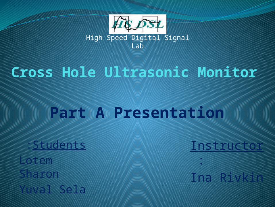
Cross Hole Ultrasonic Monitor
Part A Presentation
High Speed Digital Signal Lab
Students :Lotem SharonYuval Sela
Instructor : Ina Rivkin
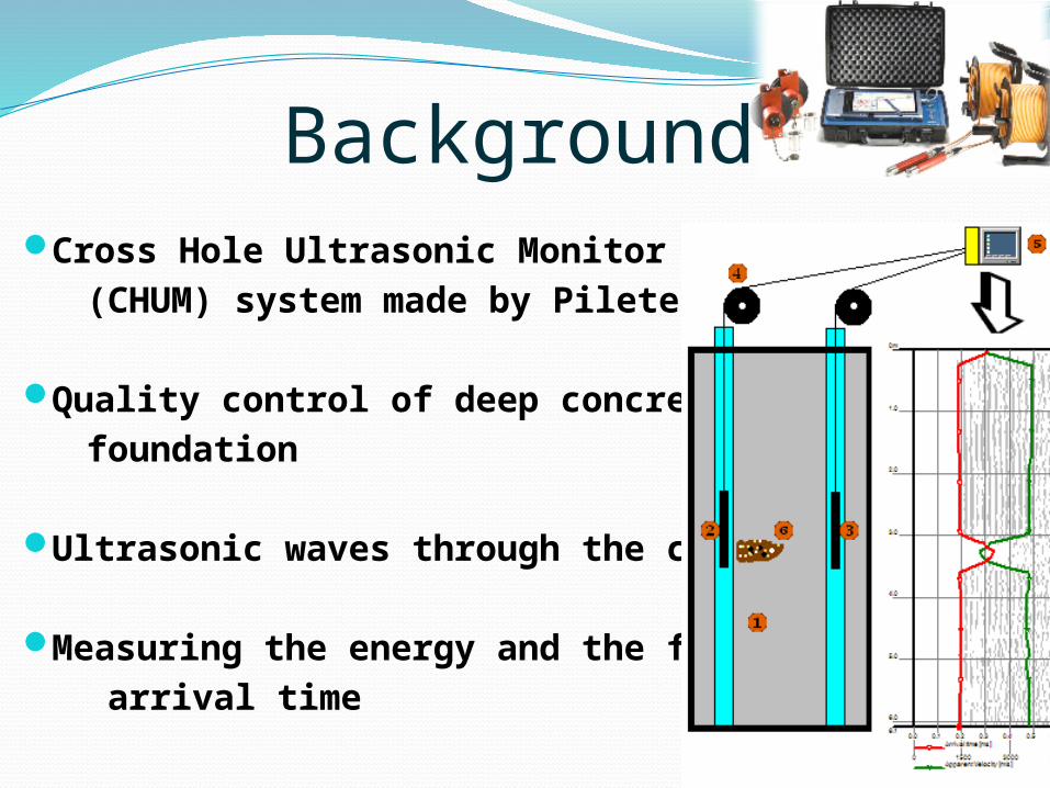
Cross Hole Ultrasonic Monitor
(CHUM) system made by Piletest
Quality control of deep concrete
foundation
Ultrasonic waves through the concrete
Measuring the energy and the first
arrival time
Background
Motivation
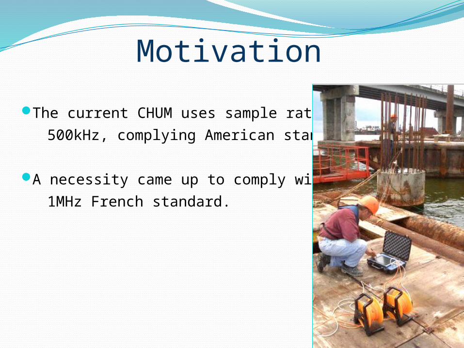
The current CHUM uses sample rate of
500kHz, complying American standard.
A necessity came up to comply with the
1MHz French standard.
GoalDeveloping a board based on FPGA, that
samples data at rates of up to 1MHz, and connects to the Motherboard.
Enabling a high sampling rate and a slow data transfer rate to the MC by FPGA configured as a FIFO and as a data flow controller.
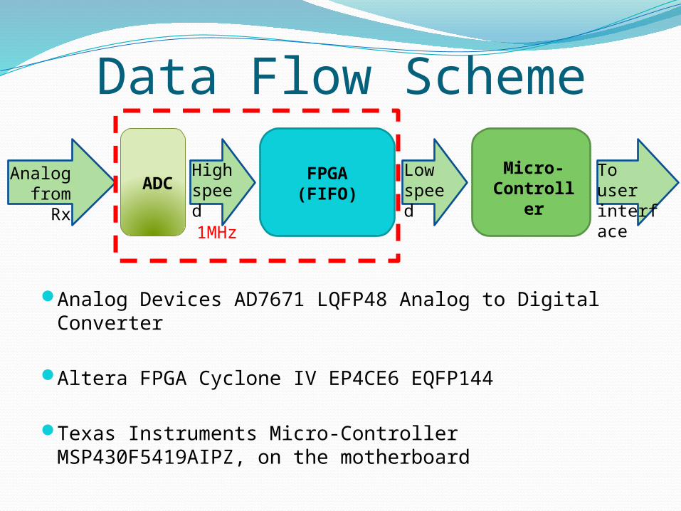
Data Flow Scheme
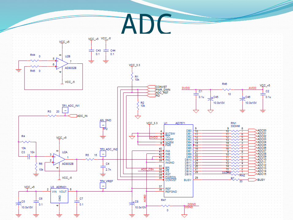
ADC
FPGA (FIFO)
Micro-Controll
er
Analog from
Rx
High speed
Low speed
To user interface
Analog Devices AD7671 LQFP48 Analog to Digital Converter
Altera FPGA Cyclone IV EP4CE6 EQFP144
Texas Instruments Micro-Controller MSP430F5419AIPZ, on the motherboard
1MHz
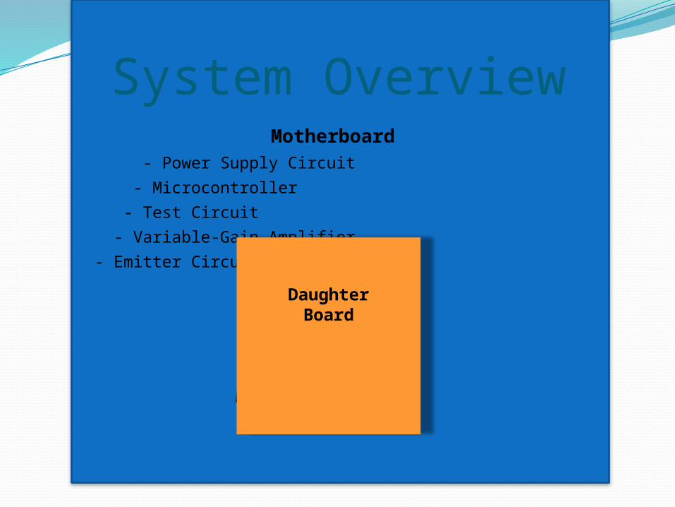
Motherboard - Power Supply Circuit
- Microcontroller
- Test Circuit
- Variable-Gain Amplifier
- Emitter Circuit
System Overview
Daughter Board
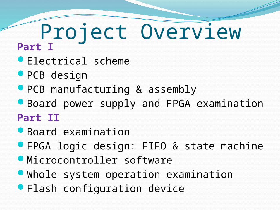
Project OverviewPart IElectrical scheme PCB designPCB manufacturing & assemblyBoard power supply and FPGA examination
Part IIBoard examinationFPGA logic design: FIFO & state machineMicrocontroller softwareWhole system operation examinationFlash configuration device
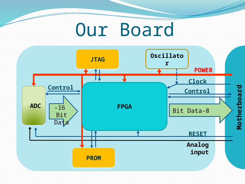
Our Board
ADC
16-Bit Data
PROM
8-Bit Data
Control
Clock
RESET
Moth
erb
oar d
JTAG
Control
POWER
Analog input
Oscillator
FPGA
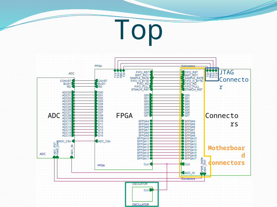
Top
Connectors
FPGAADC
JTAGConnector
Motherboard
connectors
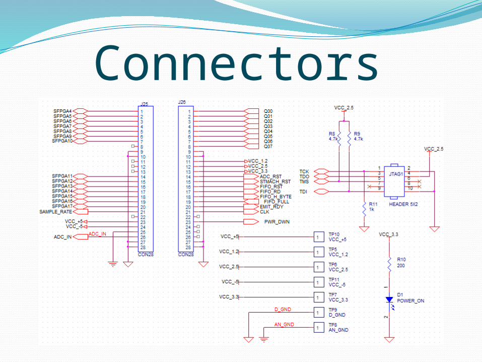
Connectors
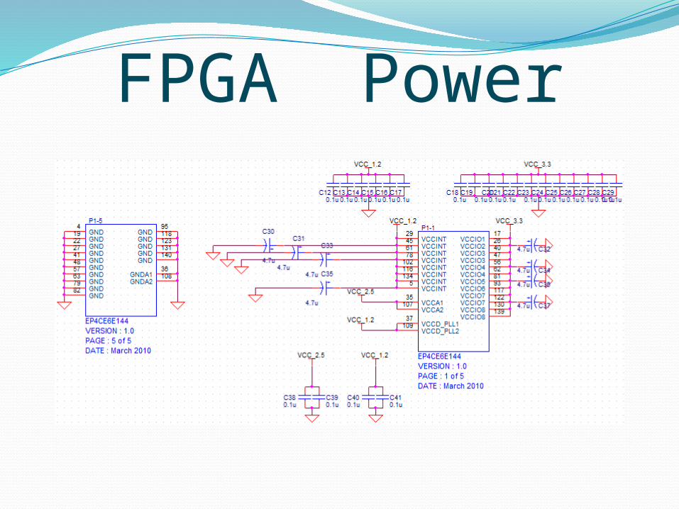
FPGA Power
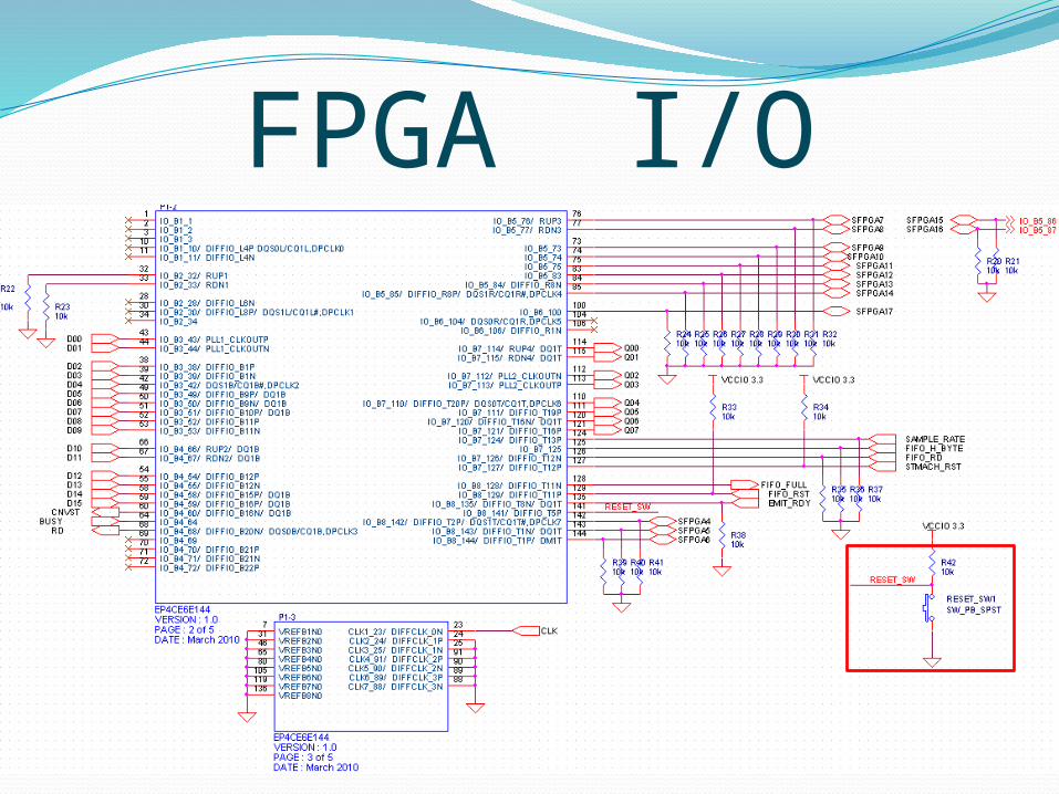
FPGA I/O
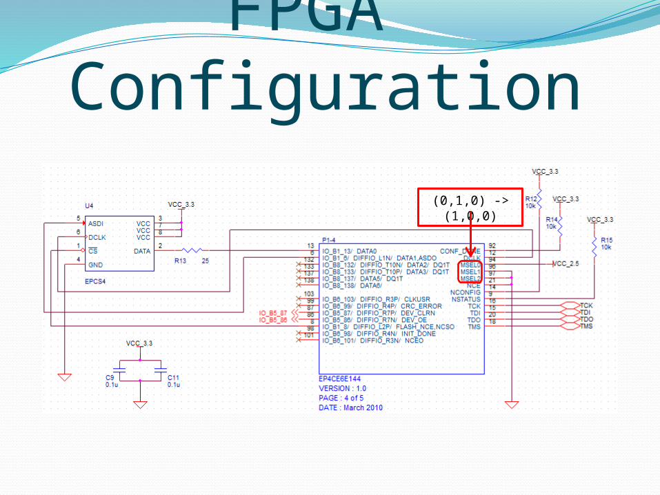
FPGA Configuration
(0,1,0) -> (1,0,0)
ADC
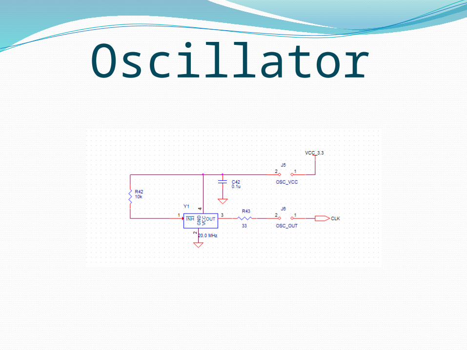
Oscillator
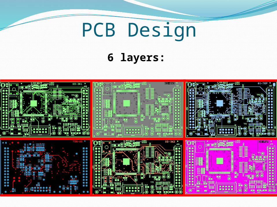
PCB Design6 layers:
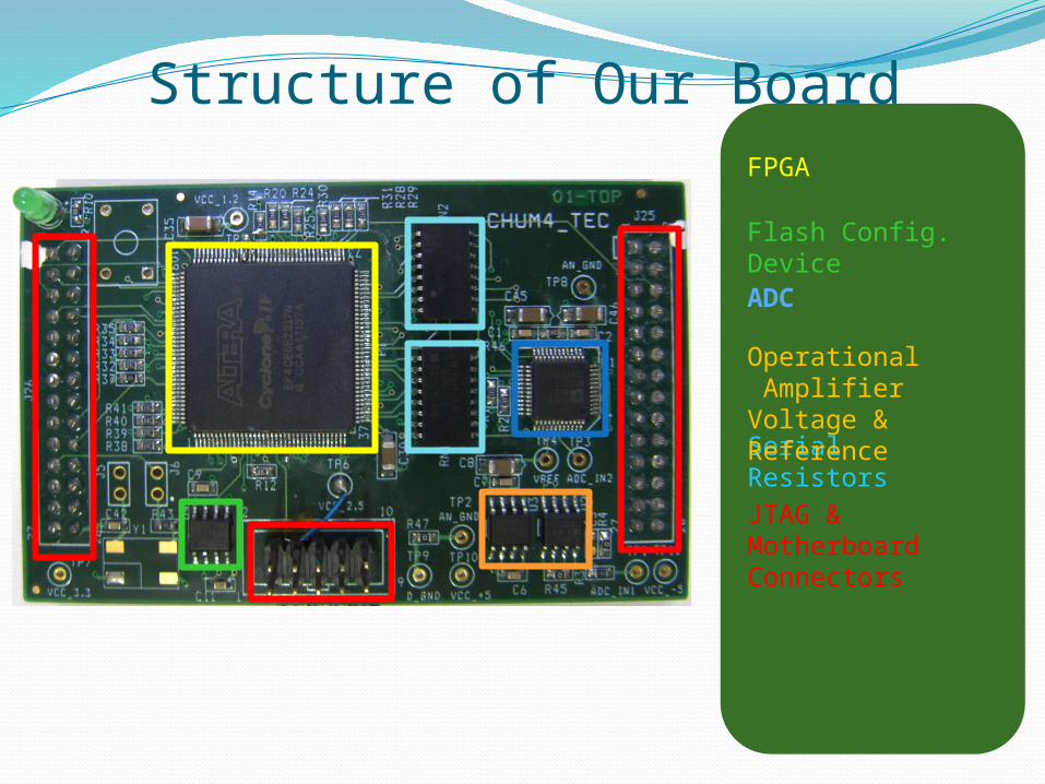
Structure of Our BoardFPGA
ADC
Flash Config. Device
JTAG & Motherboard Connectors
Serial Resistors
Operational Amplifier
&Voltage Reference
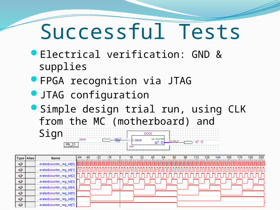
Successful TestsElectrical verification: GND & suppliesFPGA recognition via JTAGJTAG configurationSimple design trial run, using CLK from the MC
(motherboard) and SignalTap

Part B Characterization
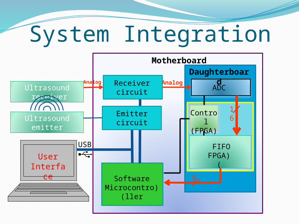
System Integration
Ultrasound receiver
Ultrasound emitter
Motherboard
ADC
Daughterboard
User Interfac
e
FIFO (FPGA
)
Control
(FPGA)
16
8Software(Microcontroll
er)
Analog
USB
Analog
Emitter circuit
Receiver circuit
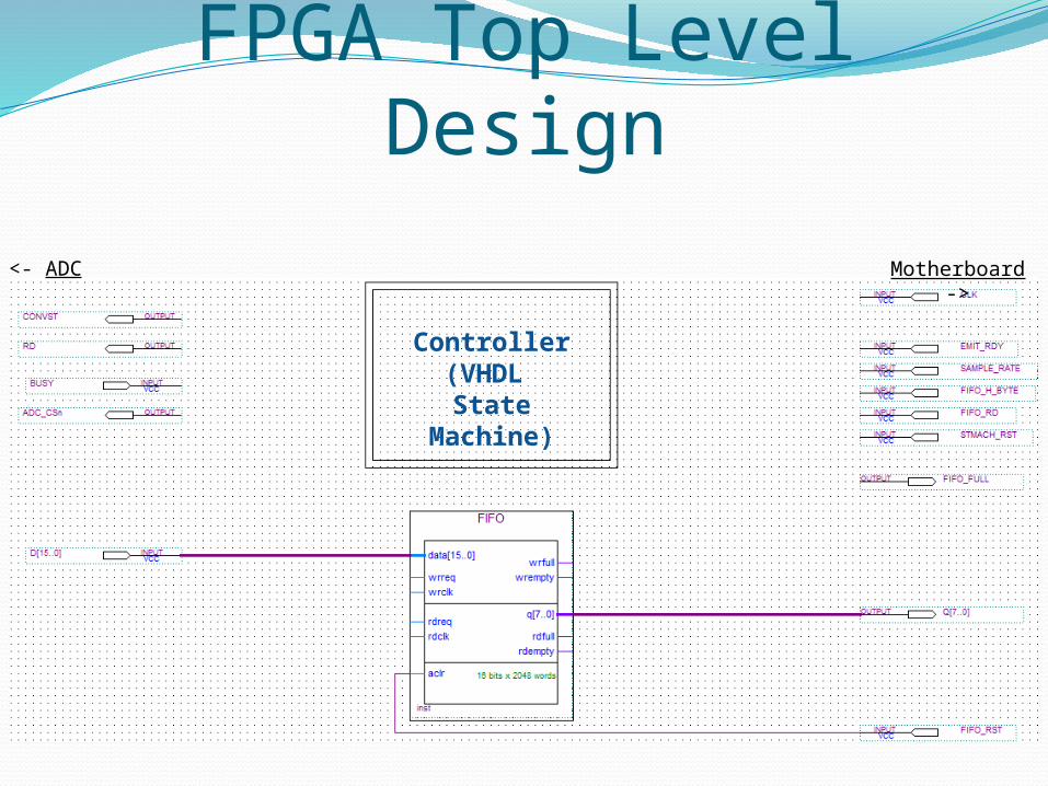
Controller(VHDL State
Machine)
FPGA Top Level Design
Motherboard ->
<- ADC
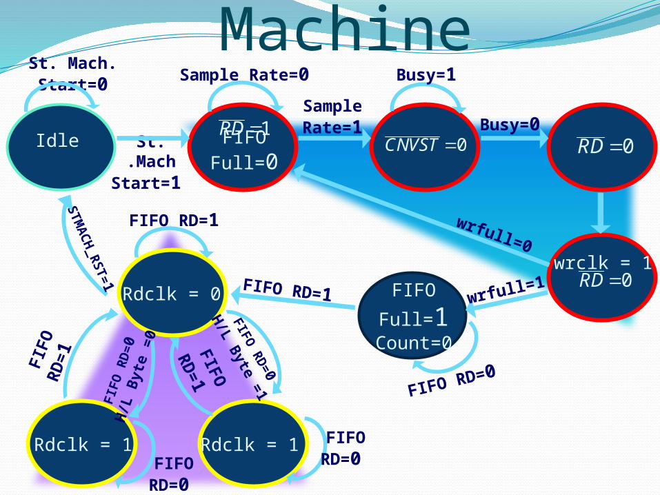
Idle
FIFO Full=0
1RD 0CNVST 0RD
wrclk = 1
0RDFIFO
Full=1Count=0
Rdclk = 1
St. Mach. Start=0 Sample Rate=0 Busy=1
St. Mach.
Start=1
Busy=0
wrfull=1
FIFO RD=0
FIFO RD=1
FIFO RD=1
FIFO RD=0
FIF
O R
D=
1
FPGA State MachineFIF
O R
D=
1
FIF
O R
D=
0H
/L B
yte
=0
FIF
O R
D=
0
H/L B
yte =1
FIFO RD=0
SampleRate=1
wrfull=0
STM
AC
H_R
ST
=1
Rdclk = 1
Rdclk = 0
Interface to UI computerData transfer from FPGA to the computerReceiver circuit gain controlEmitter controlSelf test simulation control
Microcontroller Software
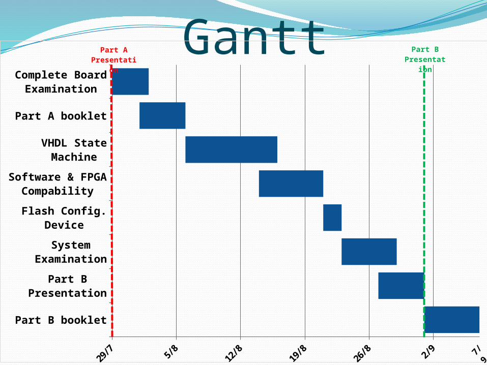
Gantt
Part B booklet
Part B Presentation
System Examination
Flash Config. Device
Software & FPGA Compability
VHDL State Machine
Part A booklet
Complete Board Examination
Part A Pre-sentation
Part B Pre-sentation