Embed Size (px)
Citation preview
Abstract - This is the second part of three parts of the above titled paper. This part will deal with maximum power transfer theorem, maximum power delivery theorem and true superposition theorem.
Keywords: Superposition theorem, maximum power transfer theorem, maximum power delivery theorem, True superposition theorem.
I. INTRODUCTIONTHE MAXIMUM power transfer theorem has received some attention by several authors [l] - [9]. References [1] - [3] deal with the maximum power transfer in multi-port networks. Hence, their description will be out of place as we will address the power transfer from a dc 2-terminal network n to another 2-terminal network N. Most of the books deal with the maximum power transferred to a variable load resistance. Very few books, for example [10] considered the maximum power delivered to a fixed load resistance. Here, all the 3 possible cases of power transfer to a resistive load [6] are considered in Section II.
However, all these are restricted to a resistance only that absorbs the power. Narayanan [7] has given a generalized form of maximum power transfer in which the element absorbing power need not be just a resistor. The theorem can be stated as: the maximum power is transferred from a 2-terminal network n to another 2-terminal network N when voltage across N equals half the open circuit voltage of n or current through N becomes half of the short circuit current of n. Narayanan Proof of the theorem [7] and an alternative proof [9] are given in Section III.
Leach [11] found that 20 introductory books on circuit analysis [12-31] either state or imply that principle of superposition (POS) on dependent sources is not allowed, which, he contended, is a misconception. He finally concluded that POS can be applied to such networks also, through a formal proof followed by several examples. In this paper, we give a general condition on the circuits to which POS cannot be applied.
A simple, but convincing proof [32] is provided in Section IV. The results are verified by the matrix method [33]. Finally, it is shown that the matrix method is more efficient [33-34].
II. MAXIMUM POWER TRANSFER THEOREMIt is desired to maximize the power in a load resistance RL when only one resistance is variable. One of the steps in evaluating the power transferred to RL is to find the Thevenin Equivalent across RL. This is shown in Figure 16 where RT and VT are the Thevenin Resistance and Thevenin Voltage, respectively.
The power delivered to RL is given by
(37)
The power will be maximum/minimum with respect to a variable ,x when
(38)
i.e., when (39)
Cases of power transfer: Since there are three variables, RL, RT and VT, the following are the possible combinations. A) RL alone is variable
B) TR alone is variable C) VT alone is variable
D) RL and TR both are variable
E) VT and TR both are variable F) VT and RL both are variable
G) VT, TR and RL are variables
Figure 16: Reduced circuit using Thevenin theorem.
Circuit Theorems – Scope and Limitations(Part II: Maximum power delivery and superposition theorems)
Dr. T. S. Rathore, Senior Member, IEEESchool of Electrical Engineering Sciences, Indian Institute of Technology, Goa, Farmagudi, Ponda, Goa 403401, India
.2 22
2
2
DN
RRRRRV
RRR
VP
LLTT
LT
LLT
T
=++
=
+
=

2
AKGEC INTERNATIONAL JOURNAL OF TECHNOLOGY, Vol. 9, No. 1
Since one and only one resistance is allowed to vary, and VT and TR do not depend upon RL, cases D, E, F and G are not possible. If VT is a variable as a function of some resistance, then TR being the ratio of open circuit voltage (VT) and short circuit current also varies with R. Thus case C does not exist. The remaining three cases will be considered now.
Case (i): LR alone is variableThe power will be maximum/minimum, using eqn. (39), when
(40)
i.e., when
This leads to the condition
This result is explicitly covered in the maximum power
transfer theorem which states that the power transfered in LR
is maximum when LR equals RT. Case (ii): When RT alone is variableThe power P will be maximum/minimum when, from eqn. (39),
i.e., when RT = -RL. Note from eqn. (37) that P decreases as RT increases. Hence if R is to be a non-negative resistor then RT = 0 will give the maximum power. Thus the conditions for maximum power in cases (i) and (ii) are different.
Example 1: Consider the circuit shown in Figure 17(a). This comes under Case 1.
The above procedure indicates that the power transferred to the combination of load resistance RL and Ro will be maximum when their parallel equivalent resistance equals R. But this condition will not necessarily give the maximum power in RL. Drawing the Thevenin equivalent circuit as shown in Fig. 17(b), and applying the above theory, we see that the power is maximum when RL = RRo/(R+Ro).
(a) (b)
Figure 17. (a) Circuit for Example 1, (b) Reduced circuit.
Example 2: Consider the circuit shown in Figure 18.
This belongs to Case (ii). Here the power delivered in LRwill be maximum when equivalent resistance of the parallel combination of R and Roequals 0, i.e., when R = 0.
Figure 18. Circuit for Example 2.
Case (iii): When both RT and VT are variableIn Figure 16 if both VT and RT are the functions of some resistance R, then the condition for maximum/ minimum power, from eqn. (40), is
(41)
This will give the value of R for maximum/minimum power transfer to RL. Note that eqn. (41) is valid when both VT and RT are expressed as polynomials in R.
Example 3: Consider the circuit shown in Fig.19. First we determine its Thevenin equivalent. The open circuit voltage VT and short circuit current IS are determined using loop analysis as follows. Applying KVL to the circuit of Fig.20 when terminals XY are open, we get
By Cramer rule,
.22
2
222
2
LRTRTV
LRLRTRTRLRTV
+=
++
.TL RR =

3
(42)
and
(43)
Thus
(44)
Figure 19. Circuit for the Example 3.
Again applying KVL to the circuit of Fig.19 when terminals XY are shorted, and IS is the clockwise loop current in loop DBCY, we get
By Cramer Rule,
Now
(45)
Note from eqns. (44) and (45) that both VT and RT are the functions of R.
Now P is given by
(46)
where
both are the polynomials in R. The condition for maximum/minimum power, from eqn. (39), is
This does not yield a solution for R. It implies that P is a monotonic function. From eqn. (46), we see that P increases as R increases. Hence it will be minimum when R = 0 and maximum when R = ∞. Thus the maximum value is
Example 4: Consider the circuit shown in Figure 20(a). It has one controlled source. We shall first find the Thevenin equivalent for the circuit. Then the condition for maximum power transferred can be obtained from eqns. (40) or (41). We shall find out the Thevenin equivalent by two alternative methods: Applying an external voltage source and finding the current supplied by this source by loop method, and by applying an external current source and again solving by the loop method.
External voltage source and loop analysisLet a voltage source be connected across terminals XY as shown in Figure 21(b). Loop currents are also shown in the figure. Note that
(47)After converting both the current sources into voltage sources,
.2
)32(++
==RR
IVR
S
TT
;)2('),1(01' RLRTRRTV +=+=
.1 1IxI −=
MAXIMUM POWER DELIVERY AND SUPERPOSITION THEOREMS

4
AKGEC INTERNATIONAL JOURNAL OF TECHNOLOGY, Vol. 9, No. 1
the circuit becomes as shown in Figure 20(c). KVL gives
Substituting for Ix from (47),
(a)
(b)
(c)
(d)
Figure 20.(a) Circuit for example 4. (b) A voltage source is applied across XY (c) Current sources converted into voltage sources (d) Thevenin Equivalent.
By Cramer rule,
(48)
Figure 20(d) gives the circuit after replacing the circuit to the left of XY by its Thevenin equivalent. Now
(49)
Comparing eqns (48) and (49) we get
(50)
Now P is given by
(51)
where both are the polynomials in R. The condition for maximum/minimum power, from eqn. (39), is
This does not yield any finite value for R. This implies that P is a monotonic function. From eqn. (51), we see that P increases as R increases. Hence it will be minimum when R = 0 and maximum when R = ∞. Thus the maximum power is
= 36 when RL = 1.
VT and RT are given by eqn.(50).

5
(56)
This will be maximum/minimum when, from eqn.(39),
(57)
It can be seen that this does not yield the value of R. Thus P is a monotonic function. Its value at R = 0 and R = ∞ are respectively
(58)
Thus P will increase from P(0) to P(∞) if P(0) <P(∞), i.e., when
,
i.e., when
(59)
From eqns.(58) and (59), we observe that
(60)
B. External current source and loop analysisExternal current source is applied across XY as shown in Figure 21(a). Converting the current sources into voltage sources, we get the circuit shown in Fig. 21(b).
By KVL
Now(52)
However, from eqn. (3), (here current I is negative)
(53)
Comparing this with eqn. (49), we get the same values of the VT and RT given by eqn.(50).
We shall take a general case of Examples 3 and 4. From eqn.(53),
(54)
In general . I = aV + b Thus, comparing we get
a. bTVaTR /,/1 −=−=
It is obvious that both TR and TV have the same denominator a. Thus we may express
(55)
where u, v, w, x, y and z are constants.
Now
(a)
(b)Figure 21 (a) Current source applied
(b) Current sources converted into voltage sources.
MAXIMUM POWER DELIVERY AND SUPERPOSITION THEOREMS
6
AKGEC INTERNATIONAL JOURNAL OF TECHNOLOGY, Vol. 9, No. 1
From eqn.(60), we note that1. The maximum/minimum power occurs when either R =
0 or R = ∞, i.e., when either R is short circuited or open circuited.
2. For positive values of ,LR 0)( >RP and vice versa.3. When u = v, w = x, y = z, P(0) = P(∞). In this case both VT
and RT become independent of R. It is also possible that P(0) may be equal to P(∞) for some value of RL. In both the cases, the power will be constant (independent of R). Readers may find some interesting application of this property.
The above results are summarized in the form of the following theorem.
Theorem: In Figure 1, if Thevenin components
then the power in
RL increases with increase in R for LR >0 and for
otherwise decreases,
and remains constant when
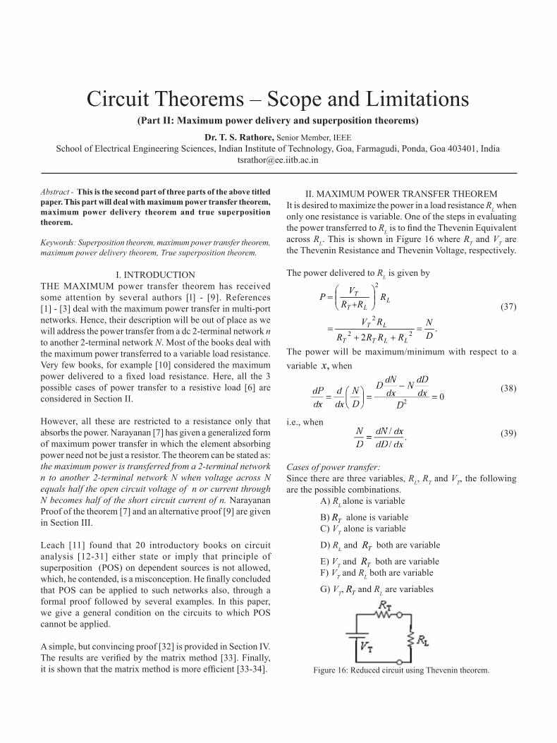
In example 3, we have u = v = 10, w =1, x = y = 2, z = 3.
From eqn. (58) P(0) = and
P(∞) =
P(0) has zeros at RL = 0 and ∞, two
poles at RL = –3/2 and peak at RL = 1.5; while P(∞) has zeros at RL = 0 and ∞, poles at RL = –2 and peak at RL = 2. From these values, the plots of both P(0) and P(∞) versus RL are drawn in Fig.22. It can be seen that the maximum power (infinite) is delivered by RL = –1.5 when R is shorted or by RL = -2 when R is opened. However, the maximum power 12.5 is delivered to RL when its value is 2 and R is opened.
Figure 22. Variation of P(0) and P(∞) versus RL for the circuit of Example 3.
Figure 23. Variation of P(0) and P(∞) versus RL for the circuit of Example 4.
Since P(0) and P(∞) curves intersect, other than at the trivial cases RL = 0, ∞, at RL = –1, –5/3 giving P(0) = P(∞). Hence, this circuit delivers constant power –100 for RL = –1 and -1500 for RL = –5/3.
In Example 4, u = –18, v = 0, w= 1, x =-8, y = –4, z = –32.
From eqn (58) P(0) = 0 and P(∞) =
P(0) has zeros at RL= 0 and ∞; while P (∞) has zeros at RL= 0 and ∞, two poles at RL = 4 and a peak at RL = –4. From these values, the plots of both P(0) and P(∞) versus RL are drawn in Fig. 10. It can be seen that the maximum power (infinite) is delivered to RL when its value is 4. Since P(0) and P(∞) curves do not intersect, except at the trivial cases RL= 0, ∞, P(0) ≠ P(∞) for RL ≠ 0, ∞. Hence, this circuit does not deliver constant power for any value of RL.
III. GENERALIZED MAXIMUM POWER DELIVERY THEOREM
Consider the circuit shown in Fig. 24 where 2-terminal network n is delivering the power to 2-terminal network N. Network n is shown by its Thevenin equivalent where vT is Thevenin voltage equal to open circuit voltage voc and RT is the Thevenin resistance = open circuit voltage voc/short circuit current isc. KVL gives
(61)
Plot of eqn. (61) is shown in Fig. 26. Note that it has a negative slope being power delivery. The interconnection of networks n and N is across terminals AB. Hence both will have the same voltage v and current i. The v-i characteristics of N will have positive slope to receive power. It is therefore necessary that v-i characteristic 2 of N should intersect at a point p as shown in Fig. 26. The power delivered by n to N is given by
P = vi. (62)
ocTTT viRviRv +−=+−=

7
After substituting for v from eqn. (61), the condition for maximum p, mentioned in the theorem, is obtained in the usual manner using differentiation etc.
An alternative proof [9] is given below.
Figure 24. Circuit with network n replaced by Thevenin Equivalent and 2-termnal network N connected.
Figure 25. v-i characteristics of n (1) and N (2).
Alternative Proof of the Generalized Maximum Power Transfer Theorem In Fig. 25 N, as per substitution theorem, is replaced by a voltage source of value v as shown in Fig. 26. Now current i can be expressed as
(63)
Substituting for RT = voc/isc and vT = voc
Figure 26. Circuit of Fig 24 with 2-termnal network N replaced by a voltage source v.
(64)
Now power absorbed by the N is
Power p will be maximum when
(65)
Now from eqn. (64)
(66)
Results of eqns. (65) and (66) can be stated in the following generalized maximum power transfer theorem.
Generalized maximum power transfer theorem: The maximum power will be transferred from a 2-terminal network n to another 2-terminal network N when voltage across (current through) N equals half of open circuit voltage (half of short circuit current) of network n.
The above theorem can also be proved by connecting a current source i instead of v.
The essential difference in the present derivation and that due to Narayanan is that instead of keeping the network N intact, we replace it by either a voltage source v (or a current source i) for finding power p which is more convincing. Note that the theorem gives the values of voltage and current for maximum power which are solely decided by network n. The actual device which will absorb the maximum power will be decided by the v-i characteristic of the network N.
Example 5: Find the conditions when the 2-terminal network N shown in Fig. 27 receives the maximum power under the following cases: N is (a) a current source, (b) a voltage source (c) resistance (d) a series resistance R and a voltage source of 7.5 V (e) a nonlinear device which has v-i relation v = ki2.
Here voc = 30 V and isc = 30/2 = 15 A. For maximum power to be delivered to N, voltage across it should voc/2 = 30/2 =15 V or current should be isc/2 = 15/2 = 7.5 A.
Figure 27. Given circuit.
Current source: Current through N for maximum power should be isc/2 = 7.5 A.
MAXIMUM POWER DELIVERY AND SUPERPOSITION THEOREMS

8
AKGEC INTERNATIONAL JOURNAL OF TECHNOLOGY, Vol. 9, No. 1
a Voltage source: Voltage across the voltage-source for maximum power should be voc/2 = 15 V.
b Resistance: When a resistance is connected, the voltage across this for maximum power to be delivered should be voc/2 = 15 V and current through it should be isc/2 = 7.5 A. Thus the resistance should be 15/7.5 = 2 which is the same given by the traditional maximum power transfer theorem.
c Series combination of voltage and resistance: For maximum power, the voltage across the combination should be voc/2 = 15 V and current through it should be isc/2 = 7.5 A. Voltage across the resistance is 15 – 7.5 = 7.5 V. Therefore the resistance should be, by Ohm’s law, 7.5/7.5 = 1 Note that the value of R equal to 1 gives the maximum power in the complete series combination of R and the 7.5–V voltage source and not in the R alone. For maximum power in R alone, its value should be
(voc/2)/(isc/2) = [(30 – 7.5)/2]/[(30–7.5)/4] = 2 .
voc/2 = k(isc/2)2→15 = k(7.5)2 →k = 4/15.
IV. SUPERPOSITION THEOREM Analysis of circuits with controlled sources using Principle of Supposition POS : We prove that POS can be applied in ‘true sense’ in solving the circuits with controlled sources. Here ‘true sense’ means that the response due to all the independent and dependent sources is obtained by superimposing the responses obtained, considering one source at a time. For convenience, without any loss of generality, we take the typical two-node network shown in Fig. 28, with current sources only as it is explained in that voltage sources, if present, can be converted into current sources. Using node analysis, one can write
(67)
Note that∑ xI and ∑ yI may or may not contain the independent and/or dependent sources depending upon the position of the current sources in the circuit. In the circuit shown, node X has the independent current source I only while node Y has both the independent current source I and dependent current source kVx. Eqn. (67) can be rewritten as
Figure 28. Typical 2-node network.
(68)
where Ri is the response due to the independent source I and Rd is that due to the dependent source kVx. It is obvious from eqn (68) that the node voltages can be solved by the POS. For example
(69)
where Δ = y11y22 - y122.
Here dependent source kVx should be treated as an independent source of value kVx where Vx is the full and final value, i.e., when all the sources (independent and dependent) are present. Hence, it can be deactivated without reducing the controlling variable Vx to zero while determining the response due to the independent source I, like we do not put any current through, or voltage across, any element 0 while deactivating an independent source.
Solving for Vx from eqn. (69), one gets
(70)
Similarly, from eqn. (68), by Cramer’s rule, one gets
Substituting for Vx from (70), and simplifying
(71)
Now we solve the circuit by the matrix method of [23]. Equation (68) can be expressed as
which yields

9
On solving one gets
(72)
and (73)
Equations (72) and (73) are the same as eqns (70) and (71), respectively. Thus, we conclude that POS can be applied to linear circuits with controlled sources also.
In [11], it is mentioned that POS cannot be applied to networks when all the sources but one are deactivated and the resulting circuit contains a node at which the voltage is indeterminate or a branch in which the current is indeterminate. In such cases POS cannot be used even if all sources are independent. We state this condition in a more general form. POS cannot be applied to circuits with or without independent sources when all the sources but one are deactivated, the activated source should not become open if it is a current source or short if it is a voltage source. Two examples of such circuits are shown in Figs. 29(a) and (b) where the current source is opened and the voltage source is shorted, respectively. The circuit in Fig. 1 is solvable when one of the current sources, say I3 is a dependent source such that I3 = I1 + I2 (requirement of KCL). If we further make that I3 = gV , the circuit becomes unsolvable because two constraints on I3 cannot simultaneously be satisfied. Similarly, the circuit shown in Fig. 29(b) is solvable when one of the voltage sources, say VCA, is a dependent source such that VCA = -(VAB + VBC) (requirement of KVL), but becomes unsolvable whenVCA is also dependent on some other voltage or current in the circuit.
(a) (b)
Figure 29. Circuits not solvable by POS.
Example 6: Determine the output voltage Vo in the circuit shown in Fig. 30.
Figure 30. Circuit for Example 1.
Applying POS
Vo = V1 (due to the source Vs alone) + V2 (due to thesource AVs alone) = AVs +0=AVs.
Example 7: Find the current through G2 in Fig. 28 when G1 = 0.8 S, G2 = 0.2 S, G3 = 0.3 S, k = 0.8 S, I = 23 A. Applying POS
where
Substituting the values, one gets
By POS for Vy
Note that it is easier to solve for the controlling variable Vx by POS first and then any other voltage or current, if required, by any other method including using POS.
Example 8: Determine current I in the circuit shown in Fig. 31.
Figure 31. Circuit for Example 8.By POS,
Example 9: Consider the circuit shown in Fig. 32. This circuit cannot be solved by series-parallel reduction, current and voltage division and Ohm’s law. We solve it by matrix method [33].
By POS and using node analysis, one gets
MAXIMUM POWER DELIVERY AND SUPERPOSITION THEOREMS

10
AKGEC INTERNATIONAL JOURNAL OF TECHNOLOGY, Vol. 9, No. 1
This is the correct answer verified by other method.
If a network does not have a single independent source, but has dependent sources only, then from eqn. (68), we see that Ri= 0 and consequently, Rd will also be zero. It means that, in the absence of any independent source, the circuit is dead, i.e., no current through, and voltage across, any element exist, even though the dependent source(s) may be present.
Figure 32. Circuit for Example 4. While determining Thevenin equivalent of a circuit without any independent source but with dependent source, both the open circuit voltage and the short circuit current will be zero as explained above. In such a case, Thevenin resistance would be indeterminate using the relation Rth = Voc/Isc =0/0. However, if we connect an independent voltage (current) source of value V (I) at the output terminalsand find the current I flowing into the voltage source (voltage drop V developed across the current source), then Rth = V/I.
Example 10: Find the Thevenin equivalent of the circuit across the terminals AB shown in Fig. 33(a).
We connect a voltage source at the terminals AB. By POS
(a) (b)
Figure 33. (a) Circuit for Example 10, (b) Circuit with external voltage source connected.
Example 11: Determine the node voltages Va and Vb in the circuit shown in Fig. 34(a). There are two dependent sources; one is controlled by a voltage Vo and the other by current Io which require the evaluation of corresponding difference of two node voltages. Such controlling variables almost double the complexity of the solution by POS.
We apply the node analysis. By POS, one gets
(a)
(b)Figure 34. (a) Circuit for Example 6 and (b) reduced circuit
(74)
(75)
(76)
11
(77)
From eqns. (76) and (77), by Cramer’s rule
Substituting the values of Vo and Ioin eqns. (76) and (77) one gets
Va=10V, Vb = 2V.
Now let us solve the same problem by Matrix method [33]. Node analysis gives
By Cramer’s rule
These are the same as obtained above, but with considerably less effort in solving.
Comparison with Other MethodsThere is a similarity between the methods based on POS and Miller equivalents [34]. In the former method, the sources are dependent while in the latter method, the elements are dependent on some parameter. However, in both the methods,
one has to determine the controlling variables first and then any other desired voltage or current. As proved in [34], matrix method is more efficient than the Miller equivalent approach. It is also more efficient than the method based on POS. This is proved below.
Let there be N number of unknown nodes and Si andSd be the number of independent and dependent sources, respectively, in a circuit. We shall compare the number of determinants to be solved by the POS method and the matrix method for determining the voltages of N nodes. In POS method, N equations for N node voltages in terms of controlling variables are to be written invoking POS. These relations require N(Si+ Sd) + 1 determinants of the order NN × to be solved. After this Sd relations among the controlling variables will be determined. Then evaluation of the controlling variables from these relations requires Sd +1 determinants of order Sd×Sd to be solved. After this the voltages of N unknown nodes are evaluated. Thus in the above example, since N = 2, Si = 1 and Sd = 2, it requires 10 determinants of order 2×2 to be solved.
Matrix method requires only N + 1 determinants of order NN × to be solved. Thus, it requires only 3 determinants as
against 10 by POS for the circuit of example 6. There is no need to determine the controlling variables explicitly. Thus the matrix method is more efficient, easier and straight forward.
V. CONCLUSIONThree possible cases of maximum power transferred to a load in a circuit where only one resistance is variable, have been brought out. Only in of the cases when the load resistance is variable the maximum power transfer theorem can be applied. In other two cases, when the load resistance RL is fixed, power has to be calculated from the first principle. Conditions for maximum power transfer have been derived for these cases. A case when both the Thevenin Voltage and Thevenin Resistance are variable has been studied in detail. The maximum/minimum power is obtained when either R = 0 (short circuit) or ∞ (open circuit). When RL is positive it absorbs the power; while negative it delivers the power to the circuit. Either power can be infinite, constant irrespective of the variable resistance, and finite for specific values of RL. This result has been stated in the form of a theorem. Theory has been explained with the help of typical examples.
A generalized maximum power theorem has been stated and proved by two different methods.
In the text books, while solving the circuits with controlled source using POS, controlled sources are not deactivated. Thus POS has not been applied in ‘true sense’ to circuits with dependent sources. It has been shown here that POS can be applied in the ‘true sense’ to such circuits also, but with
MAXIMUM POWER DELIVERY AND SUPERPOSITION THEOREMS

12
AKGEC INTERNATIONAL JOURNAL OF TECHNOLOGY, Vol. 9, No. 1
the following caution: (i) All the dependent sources should also be treated as independent sources with their full value (contribution from all the sources). (ii) When the dependent source is deactivated, its controlling variable should not be zeroed. POS is applicable to all those circuits with dependent sources as well if it is applicable to these circuits when all the dependent sources are treated as independent sources.
REFERENCES[1] K. K. Nambiar, “A generalization of maximum power transfer
theorem”, Proc. IEEE, pp. 1339-1340, July 1969.[2] C. A. Desoer, The maximum power transfer theorem for n-ports,
Trans. IEEE Circuit Theory, pp 328-330, May 1973.[3] H. Baudrand, “On the generalization of the maximum power
transfer theorem”, Proc. IEEE, pp 1780-1781, Oct. 1979.[4] S. C. Dutta Roy, “Many faces of the maximum power transfer
theorem”, International Journal of Electrical Engineering Education, vol. 40, no. 2, pp. 103-111, April, 2003.
[5] C. S. Kong, “A general Maximum power transfer theorem”, IEEE Trans on Education, vol. 38, no. 3, pp. 296-298, August 1995.
[6] T. S. Rathore, “Conditions for maximum power transfer”, IETE J Education, vol. 54, no. 2, pp 61-74, July-Dec 2013.
[7] H. Narayanan, “On the maximum power transfer theorem”, Int. J. of Electrical Engineering, vol. 15, pp. 161-167, 1978.
[8] J. C. McLaughlin and K. L. Kaiser, “Deglorifying” the maximum power transfer theorem and factors in impedance selection”, IEEE Trans. Education, vol. 50, no. 3, pp 251 255, August 2007.
[9] T S Rathore, “Generalized Maximum Power Transfer Theorem”, IETE J of Education, vol. 58, no. 1, pp. 39-41, Jan-Jun 2017.
[10] K. V. V. Murthy and M. S. Kamath, Circuit Analysis, Jaico Publishing House, Mumbai, 8thJaico Impression, 2010.
[11] W. M. Leach, On the application of superposition to dependent sources in circuit analysis, unpublished manuscript available at http://users.ece.gatech.edu/+mleach/papers/superpose.pdfC.
[12] K. Alexander and M. N. Sadiku, Fundamentals of Electric Circuits, New York: McGraw-Hill, 2004
[13] L. S. Bobrow, Elementary Linear Circuit Analysis, New York: Holt, Rinehart and Winston, 1981
[14] R. L. Boylestad, Introductory Circuit Analysis, New York: Macmillan, 1994.
[15] A. B. Carson. Circuits: Engineering Concepts and Analysis of Linear Electric Circuits, Stamford, CT: Brooks Cole, 2000
[16] J. J. Cathey, Schaum’s Outline on Electronic Devices and Circuits, Second Edition, NY: McGraw-Hill, 2002
[17] C. M. Close, The Analysis of Linear Circuits, New York: Harcourt, Brace. & World, 1966
[18] R. C. Dorf and J. A. Syoboda, Introduction to Electric Circuits, Sixth Edition, New York: John Wiley, 2004
[19] A. R. Hambley, Electrical Engineering Principles and Applications, Third Edition, Upper Saddle River, NJ: Pearson Education, 2005
[20] W. H. Hayt Jr., J. E. Kimmerely and S. M. Durbin, Engineering Circuit Analysis, New York: McGraw-Hill, 2002
[21] M. N. Horenstein, Microelectronic Circuits and Devices, Englewood Cliffs, NJ: Prentice-Hall, 1990
[22] D. E. Johnson, J. L. Hilburn, J. R. Johnson and P. D. Scott, Basic Electric Circuit Analysis, Englewood Cliffs, NJ: Prentice-Hall, 1995.
[23] R. Mauro, Engineering Electronics, Englewood Cliffs, NJ: Prentice-Hall, 1989.
[24] R. M. Mersereau and Joel R. Jackson, Circuit Analysis: A system Approach, Upper Saddle River, NJ: Pearson/Prentice Hall, 2006.
[25] M. Nahavi and J. Edminister, Schaum’s Outlines on Electric Circuits, Fourth Edition, NY: McGraw-Hill, 2003.
[26] J. W. Nilsson and S. A. Riedel, Electric Circuits, Seventh Edition, Englewood Cliffs, NJ: Prentice-Hall, 2005.
[27] M. Reed and R. Rohrer, Applied Electric Circuit Analysis for Electrical and Computer Engineers, Upper Saddle River, NJ: Prentice-Hall, 1999.
[28] A. H. Robins and W. C. Miller, Circuit Analysis: Theory and Practice, Third Edition, Clifton park, NY: Thomson Delmar Learning, 2004.
[29] R. E. Scott, Linear Circuits, New York: Addison-Wesley, 1960.[30] K. L. Su, Fundamentals of Circuit Analysis, Prospect Heights,
IL: Waveland Press, 1993.[31] R. E. Thomas and A. J. Rosa, The Analysis and Design of Linear
Circuits, Second Edition, Upper Saddle River, NJ: Prentice-Hall, 1998.
[32] T S Rathore, K Jayasudha and Sunita Sharma, “Analysis of electrical circuits with controlled sources through the principle of superposition”, Int J Engineering and Technology , Feb 2012
[33] T. S. Rathore and G. A. Shah, “Miller equivalents and their applications”, Int J Circuits, Systems and Signal Processing, Birkhauser, Boston, vol. 29, pp. 757-768, July 2010.
[34] Tejmal S. Rathore and G. A. Shah, “Matrix approach: Better than applying Miller’s equivalents”, IETE J Edn, vol. 51, no. 2&3, pp. 85-90, May-December 2010.
Dr. T S Rathore received B Sc (Engg), ME, and PhD (Electrical Engineering) all from Indore University, Indore.
He served SGSITS, Indore (1965-1978), IIT Bombay (1978-2006), and St. Francis Institute of Technology, Borivali (2006-2014) as Dean (R&D). Currently, he is a visiting professor at IIT Goa, India since July 2017.
He was a post-doctoral fellow (1983-85) at the Concordia University, Canada and a visiting researcher at the University of South Australia, Adelaide (March-June 1993). He was an ISTE visiting professor (2005-2007). He has published and presented over 225 research papers. He has authored the book Digital Measurement Techniques, New Delhi: Narosa Publishing House, 1996 and Alpha Science International Pvt Ltd., UK, 2003 and translated in Russian language in 2004. He was the Guest Editor of the special issue of Journal of IE on Instrumentation Electronics (1992). He is a member on the editorial boards of ISTE National Journal of Technical Education and IETE Journal of Education.
Prof. Rathore is a Life Senior Member of IEEE, Fellow of IETE and IE (India), Member of ISTE, Instrument and Computer Societies of India. He has served Mumbai Centre as Secretary, Vice-Chairman and Chairman. He received IEEE Silver Jubilee Medal, ISTE U P Government National Award (2002) and Maharashtra State National Award (2003), IETE M N Saha Memorial Award, Prof S V C Aiya Memorial Award, BR Batra Memorial Award, Prof K Sreenivasan Memorial Award, K S Krishnan Memorial Award, Hari Ramji Toshniwal Gold Medal Award, and best paper awards published in IETE J of Education (2011, 2013).
His fields of teaching and research interests are Circuit Theory, Electronic Instrumentation, Signal Processing, SC Filters, Analog and Digital Circuits.


![Circuit Theorems [相容模式] - National Chiao Tung University · 2012. 10. 5. · Circuit Theorems •Introduction •Linearity Property •Superposition •Source Transformation](https://img.pdfslide.net/doc/110x75/5ffa33782109f15b771b8b05/circuit-theorems-c-national-chiao-tung-2012-10-5-circuit-theorems.jpg)


![BMS COLLEGE OF ENGINEERING, BANGALORE Syllabus 2009-12.pdf · Superposition, Reciprocity, Millman’s Thevinin’s and Norton’s theorems, Maximum Power transfer theorem. [12 Hours]](https://img.pdfslide.net/doc/110x75/5ebb32f790d45c1c153de3ec/bms-college-of-engineering-bangalore-syllabus-2009-12pdf-superposition-reciprocity.jpg)