Embed Size (px)
Citation preview

Data Sheet
1
Mar. 2012 Rev. 2. 0 BCD Semiconductor Manufacturing Limited
DUAL 300mA LDO REGULATORS AP2402
General Description
The AP2402 series are dual positive voltage regulatorICs fabricated by CMOS process. Each of these ICsconsists of a voltage reference, two error amplifiers,two resistor networks for setting output voltages. Eachchannel has a current limit circuit for current protectionand a chip enable circuit with quick discharge function.
The AP2402 series feature high supply voltage ripplerejection, low dropout voltage, low noise, high outputvoltage accuracy, and low current consumption whichmake them ideal for use in various battery-powereddevices. The chip-enable function allows the output ofeach channel to be turned on/off independently, greatlyreducing the power consumption.
The AP2402 series have 2.5V/1.8V, 2.8V/1.8V, 2.8V/2.8V, 2.8V/3.3V and 3.3V/3.3V versions.
The 2.5V/1.8V, 2.8V/1.8V and 2.8V/2.8V versions areavailable in SOT-23-6, TSOT-23-6 and DFN-2×2-8packages. The 2.8V/3.3V and 3.3V/3.3V versions areavailable in TSOT-23-6 package only.
Features
· Minimum Output Current Capability per Channel:300mA
· High Output Voltage Accuracy: ±2%· Low Quiescent Current per Channel: 50µA Typi-
cal· Low Standby Current: 0.1µA Typical· High PSRR: 70dB Typical (f=1kHz)· Extremely Low Noise: 30µVrms (10Hz to
100kHz) · Operating Temperature: -20 to 60oC· Compatible with 2.2µF Low ESR Ceramic Capac-
itor
Applications
· Mobile Phones, Cordless Phones· Wireless Communication Equipment · Portable Games· Cameras, Video Recorders· Sub-board Power Supplies for Telecom Equip-
ment· Battery Powered Equipment
Figure 1. Package Types of AP2402
SOT-23-6 TSOT-23-6 DFN-2×2-8
PART IS OBSOLETE PLEASE USE AP7332

Data Sheet
2
Mar. 2012 Rev. 2. 0 BCD Semiconductor Manufacturing Limited
DUAL 300mA LDO REGULATORS AP2402
Pin 1 Mark
VOUT1
Pin Configuration
Figure 2. Pin Configuration of AP2402 (Top View)
K Package (SOT-23-6)
Pin Description
Pin NumberPin Name Function
6-pin 8-pin
1 7 VOUT2 Output voltage 2
2 5 GND Ground
3 3 CE2 On/Off control 2, logic high=enable; logic low=shutdown
4 2 CE1 On/Off control 1, logic high=enable; logic low=shutdown
5 1 VIN Input voltage
6 8 VOUT1 Output voltage 1
4, 6 NC No connection
VIN GND
CE1
VOUT2
CE2
VOUT1
KT Package (TSOT-23-6)
DN Package (DFN-2×2-8)
VIN GND
CE1
VOUT2
CE2
1
2
3
4
6
5
7
8 VIN
CE1
CE2
NC GND
NC
VOUT2
VOUT11
2
3 4
5
Pin 1 Mark
6 1
2
3 4
5
Pin 1 Mark
6
PART IS OBSOLETE PLEASE USE AP7332

Data Sheet
3
Mar. 2012 Rev. 2. 0 BCD Semiconductor Manufacturing Limited
DUAL 300mA LDO REGULATORS AP2402
ErrorAmplifier 2
ErrorAmplifier 1
On/OffControl
On/OffControl
VoltageReference
CE1
CE2
GND
VIN
VOUT1
VOUT2
VR1Each Circuit
VR2Each Circuit
Current Limitand ThermalProtection
Current Limitand ThermalProtection
Shutdownand Logic
Control
Functional Block Diagram
Figure 3. Functional Block Diagram of AP2402
4 (2)
5 (1)
3 (3)
1 (7)
2 (5)
6 (8)
A (B)A for 6-pinB for 8-pin
PART IS OBSOLETE PLEASE USE AP7332

Data Sheet
4
Mar. 2012 Rev. 2. 0 BCD Semiconductor Manufacturing Limited
DUAL 300mA LDO REGULATORS AP2402
Ordering Information
Package Temperature Range
Output Voltages
Part Number Marking ID Part Number Marking
IDPacking Type
Lead-Free Lead-Free Green Green
SOT-23-6 -20 to 60oC
2.5V/1.8V AP2402A21KTR-E1 EAA AP2402A21KTR-G1 GAA Tape & Reel
2.8V/1.8V AP2402A31KTR-E1 EAB AP2402A31KTR-G1 GAB Tape & Reel
2.8V/2.8V AP2402A33KTR-E1 EAC AP2402A33KTR-G1 GAC Tape & Reel
TSOT-23-6 -20 to 60oC
2.5V/1.8V AP2402A21KTTR-E1 S8A AP2402A21KTTR-G1 L8A Tape & Reel
2.8V/1.8V AP2402A31KTTR-E1 S8B AP2402A31KTTR-G1 L8B Tape & Reel
2.8V/2.8V AP2402A33KTTR-E1 S8C AP2402A33KTTR-G1 L8C Tape & Reel
2.8V/3.3V AP2402A34KTTR-E1 S8D AP2402A34KTTR-G1 L7A Tape & Reel
3.3V/3.3V AP2402A44KTTR-E1 S8F AP2402A44KTTR-G1 L7B Tape & Reel
DFN-2×2-8 -20 to 60oC
2.5V/1.8V AP2402A21DNTR-E1 6A AP2402A21DNTR-G1 DA Tape & Reel
2.8V/1.8V AP2402A31DNTR-E1 6B AP2402A31DNTR-G1 DB Tape & Reel
2.8V/2.8V AP2402A33DNTR-E1 6C AP2402A33DNTR-G1 DC Tape & Reel
Circuit Type
Package
E1: Lead Free
AP2402 -
TR: Tape and Reel
Ordering Information
K: SOT-23-6
A: Active High (With Built-in Pull-down Resistor)
3: Fixed Output 2.8V (Channel 2)
2: Fixed Output 2.5V (Channel 1)3: Fixed Output 2.8V (Channel 1)
1: Fixed Output 1.8V (Channel 2)
KT: TSOT-23-6DN: DFN-2×2-8
G1: Green
BCD Semiconductor's Pb-free products, as designated with "E1" suffix in the part number, are RoHS compliant. Products with"G1" suffix are available in green packages.
4: Fixed Output 3.3V (Channel 1)
4: Fixed Output 3.3V (Channel 2)
PART IS OBSOLETE PLEASE USE AP7332

Data Sheet
5
Mar. 2012 Rev. 2. 0 BCD Semiconductor Manufacturing Limited
DUAL 300mA LDO REGULATORS AP2402
Parameter Symbol Value Unit
Input Voltage VIN 6.5 V
Enable Input Voltage VCE 6.5 V
Output Current (TA=25oC) IOUT1+IOUT2 700 mA
Power Dissipation (TA=25oC) PD SOT-23-6 250 mW
Junction Temperature TJ 150 oC
Storage Temperature Range TSTG -65 to 150 oC
Lead Temperature (Soldering, 10sec) TLEAD 260 oC
ESD (Human Body Model) ESD 6000 V
ESD (Machine Model) ESD 200 V
Absolute Maximum Ratings (Note 1)
Parameter Symbol Min Max Unit
Input Voltage VIN 6 V
Operating Ambient Temperature Range TA -20 60 oC
Recommended Operating Conditions
Note 1: Stresses greater than those listed under "Absolute Maximum Ratings" may cause permanent damage to the device.These are stress ratings only, and functional operation of the device at these or any other conditions beyond those indicatedunder "Recommended Operating Conditions" is not implied. Exposure to "Absolute Maximum Ratings" for extended periodsmay affect device reliability.
PART IS OBSOLETE PLEASE USE AP7332

Data Sheet
6
Mar. 2012 Rev. 2. 0 BCD Semiconductor Manufacturing Limited
DUAL 300mA LDO REGULATORS AP2402
Parameter Symbol Conditions Min Typ Max Unit
Output Voltage Accuracy ∆VOUT/VOUTVariation from specifiedVOUT, IOUT=30mA -2 2 %
Input Voltage VIN 6 V
Maximum Output Current IOUT(Max) 300 mA
Load Regulation VRLOAD 1mA≤IOUT≤300mA 10 60 mV
Line Regulation VRLINEVOUT+1V≤VIN≤6VIOUT=30mA, VCE=VIN
0.01 0.2 %/V
Dropout Voltage VDROP
IOUT=30mA
VOUT=1.8V 30 36
mV
VOUT=2.5V 20 24
VOUT=2.8V 20 24
VOUT=3.3V 20 24
IOUT=100mA
VOUT=1.8V 100 120
VOUT=2.5V 65 80
VOUT=2.8V 65 80
VOUT=3.3V 65 80
Quiescent Current IQ IOUT=0mA 50 90 µA
Standby Current ISTD VCE in OFF mode 0.1 1 µA
Power Supply Rejection Ratio PSRR
Ripple 0.5Vp-p, f=1kHz VIN=VOUT+1V, IOUT=30mA 70 dB
Output Voltage Temperature Coefficient
(∆VOUT/VOUT)/∆T IOUT=30mA, -20oC≤TA≤60oC ±100 ppm/oC
Current Limit ILIMIT VCE=VIN 400 mA
Short Circuit Current ISHORT VCE=VIN, VOUT short to GND 50 mA
RMS Output Noise VNOISE 10Hz≤f≤100kHz 30 µVrms
CE "High" Voltage CE input voltage "High" 1.3 6 V
CE "Low" Voltage CE input voltage "Low" 0.4 V
Thermal Shutdown 165 oC
Thermal Shutdown Hys-teresis
30 oC
Thermal Resistance(Junction to Case)
θJC
SOT-23-6 85oC/WTSOT-23-6 85
DFN-2X2-8 130
(Channel 1/Channel 2: VIN=VOUT+1V, TA=25oC, CIN=1µF, COUT=2.2µF, unless otherwise specified.)
Electrical Characteristics
PART IS OBSOLETE PLEASE USE AP7332
Data Sheet
7
Mar. 2012 Rev. 2. 0 BCD Semiconductor Manufacturing Limited
DUAL 300mA LDO REGULATORS AP2402
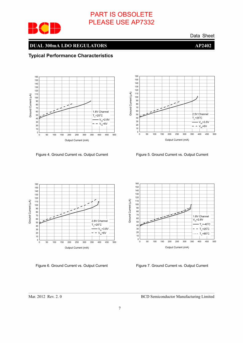
Typical Performance Characteristics
0 50 100 150 200 250 300 350 400 450 5000
102030405060708090
100110120130140150160
Gro
und
Cur
rent
(µA)
Output Current (mA)
2.8V ChannelTC=25oC
VIN=3.8V VIN=6V
0 50 100 150 200 250 300 350 400 450 5000
102030405060708090
100110120130140150160
Gro
und
Cur
rent
(µA)
Output Current (mA)
1.8V ChannelTC=25oC
VIN
=2.8V VIN=6V
0 50 100 150 200 250 300 350 400 450 5000
102030405060708090
100110120130140150160
Gro
und
Cur
rent
(µA)
Output Current (mA)
2.5V ChannelT
C=25oC
VIN=3.5V VIN=6V
Figure 4. Ground Current vs. Output Current Figure 5. Ground Current vs. Output Current
Figure 6. Ground Current vs. Output Current
0 50 100 150 200 250 300 350 400 450 5000
102030405060708090
100110120130140150160
Gro
und
Cur
rent
(µA
)
Output Current (mA)
1.8V ChannelVIN=2.8V
TC=-40oC
TC=25oC
TC=85oC
Figure 7. Ground Current vs. Output Current
PART IS OBSOLETE PLEASE USE AP7332

Data Sheet
8
Mar. 2012 Rev. 2. 0 BCD Semiconductor Manufacturing Limited
DUAL 300mA LDO REGULATORS AP2402
Typical Performance Characteristics (Continued)
0 50 100 150 200 250 300 350 400 450 5000
102030405060708090
100110120130140150160
Gro
und
Cur
rent
(µA)
Output Current (mA)
2.8V ChannelVIN=3.8V
TC=-40oC
TC=25oC
TC=85oC
0 50 100 150 200 250 300 350 400 450 5000
102030405060708090
100110120130140150160
Gro
und
Cur
rent
(µA)
Output Current (mA)
2.5V ChannelVIN=3.5V
TC=-40oC
TC=25oC
TC=85oC
Figure 9. Ground Current vs. Output CurrentFigure 8. Ground Current vs. Output Current
Figure 10. Output Voltage vs. Output Current Figure 11. Output Voltage vs. Output Current
0 30 60 90 120 150 180 210 240 270 3001.70
1.72
1.74
1.76
1.78
1.80
1.82
1.84
1.86
1.88
1.90
Out
put V
olta
ge (V
)
Output Current (mA)
1.8V ChannelVIN=2.8V
TC=25oC
0 30 60 90 120 150 180 210 240 270 3002.40
2.42
2.44
2.46
2.48
2.50
2.52
2.54
2.56
2.58
2.60
Out
put V
olta
ge (V
)
Output Current (mA)
2.5V ChannelVIN=3.5V
TC=25oC
PART IS OBSOLETE PLEASE USE AP7332

9
Mar. 2012 Rev. 2. 0 BCD Semiconductor Manufacturing Limited
Data Sheet
DUAL 300mA LDO REGULATORS AP2402
0 30 60 90 120 150 180 210 240 270 3002.70
2.72
2.74
2.76
2.78
2.80
2.82
2.84
2.86
2.88
2.90
Out
put V
olta
ge (V
)
Output Current (mA)
2.8V ChannelVIN=3.8V
TC=25oC
Figure 12. Output Voltage vs. Output Current
Typical Performance Characteristics (Continued)
0 50 100 150 200 250 300 350 400 450 5000.0
0.2
0.4
0.6
0.8
1.0
1.2
1.4
1.6
1.8
2.0
Out
put V
olta
ge (V
)
Output Current (mA)
1.8V ChannelVIN=2.8V
TC=-40oC
TC=25oC
TC=85oC
Figure 13. Output Voltage vs. Output Current
0 50 100 150 200 250 300 350 400 450 5000.0
0.4
0.8
1.2
1.6
2.0
2.4
2.8
Out
put V
olta
ge (V
)
Output Current (mA)
2.5V ChannelVIN=3.5V
TC=-40oC
TC=25oC
TC=85oC
Figure 14. Output Voltage vs. Output Current
0 50 100 150 200 250 300 350 400 450 5000.0
0.4
0.8
1.2
1.6
2.0
2.4
2.8
Out
put V
olta
ge (V
)
Output Current (mA)
2.8V ChannelV
IN=3.8V
TC=-40oC
TC=25oC
TC=85oC
Figure 15. Output Voltage vs. Output Current
PART IS OBSOLETE PLEASE USE AP7332

Data Sheet
10
Mar. 2012 Rev. 2. 0 BCD Semiconductor Manufacturing Limited
DUAL 300mA LDO REGULATORS AP2402
Typical Performance Characteristics (Continued)
0 50 100 150 200 250 300 350 400 450 5000.0
0.4
0.8
1.2
1.6
2.0
2.4
2.8
Out
put V
olta
ge (V
)
Output Current (mA)
2.8V ChannelTC=25oC
VIN=3.8V VIN=6V
0 50 100 150 200 250 300 350 400 450 5000.0
0.2
0.4
0.6
0.8
1.0
1.2
1.4
1.6
1.8
2.0
Out
put V
olta
ge (V
)
Output Current (mA)
1.8V ChannelTC=25oC
VIN=2.8V VIN=6V
0 50 100 150 200 250 300 350 400 450 5000.0
0.4
0.8
1.2
1.6
2.0
2.4
2.8
Out
put V
olta
ge (V
)
Output Current (mA)
2.5V ChannelTC=25oC
VIN
=3.5V VIN=6V
Figure 16. Output Voltage vs. Output Current Figure 17. Output Voltage vs. Output Current
Figure 18. Output Voltage vs. Output Current Figure 19. Output Voltage vs. Input Voltage
0 1 2 3 4 5 60.0
0.2
0.4
0.6
0.8
1.0
1.2
1.4
1.6
1.8
2.0
Out
put V
olta
ge (V
)
Input Voltage (V)
1.8V ChannelTC=25oC
IOUT=10mA IOUT=100mA IOUT=300mA
PART IS OBSOLETE PLEASE USE AP7332

11
Mar. 2012 Rev. 2. 0 BCD Semiconductor Manufacturing Limited
Data Sheet
DUAL 300mA LDO REGULATORS AP2402
Figure 20. Output Voltage vs. Input Voltage
Typical Performance Characteristics (Continued)
0 1 2 3 4 5 60.0
0.4
0.8
1.2
1.6
2.0
2.4
2.8
Out
put V
olta
ge (V
)
Input Voltage (V)
2.8V ChannelTC=25oC
IOUT=10mA I
OUT=100mA
IOUT=300mA
Figure 21. Output Voltage vs. Input Voltage
Figure 22. Dropout Voltage vs. Output Current Figure 23. Dropout Voltage vs. Output Current
0 50 100 150 200 250 3000
50
100
150
200
250
300
350
400
Dro
pout
Vol
tage
(mV)
Output Current (mA)
1.8V Channel TC=-40oC
TC=25oC
TC=85oC
0 1 2 3 4 5 60.0
0.4
0.8
1.2
1.6
2.0
2.4
2.8
Out
put V
olta
ge (V
)
Input Voltage (V)
2.5V ChannelTC=25oC
IOUT=10mA I
OUT=100mA
IOUT=300mA
0 50 100 150 200 250 3000
50
100
150
200
250
300
350
400
Dro
pout
Vol
tage
(mV
)
Output Current (mA)
2.5V Channel TC=-40oC
TC=25oC
TC=85oC
PART IS OBSOLETE PLEASE USE AP7332

Data Sheet
12
Mar. 2012 Rev. 2. 0 BCD Semiconductor Manufacturing Limited
DUAL 300mA LDO REGULATORS AP2402
Typical Performance Characteristics (Continued)
Figure 24. Dropout Voltage vs.Output Current Figure 25. Output Voltage vs. Case Temperature
Figure 26. Output Voltage vs. Case Temperature
-30 -15 0 15 30 45 60 752.70
2.72
2.74
2.76
2.78
2.80
2.82
2.84
2.86
2.88
2.90
Out
put V
olta
ge (V
)
Case Temperature (oC)
2.8V ChannelVIN=3.8VIOUT=30mA
Figure 27. Output Voltage vs. Case Temperature
-30 -15 0 15 30 45 60 751.70
1.72
1.74
1.76
1.78
1.80
1.82
1.84
1.86
1.88
1.90
1.8V ChannelVIN=2.8VIOUT=30mA
Out
put V
olta
ge (V
)
Case Temperature (oC)
-30 -15 0 15 30 45 60 752.40
2.42
2.44
2.46
2.48
2.50
2.52
2.54
2.56
2.58
2.60
2.5V ChannelVIN=3.5VIOUT
=30mA
Out
put V
olta
ge (V
)
Case Temperature (oC)
0 50 100 150 200 250 3000
50
100
150
200
250
300
350
400
Dro
pout
Vol
tage
(mV
)
Output Current (mA)
2.8V Channel TC=85oC
TC=25oC
TC=-40oC
PART IS OBSOLETE PLEASE USE AP7332

13
Mar. 2012 Rev. 2. 0 BCD Semiconductor Manufacturing Limited
Data Sheet
DUAL 300mA LDO REGULATORS AP2402
Figure 28. Quiescent Current vs. Input Voltage Figure 29. Quiescent Current vs. Input Voltage
Typical Performance Characteristics (Continued)
0 1 2 3 4 5 60
15
30
45
60
75
90
Qui
esce
nt C
urre
nt (µ
A)
Input Voltage (V)
2.5V ChannelNo Load
TC=-40oC
TC=25oC
TC=85oC
0 1 2 3 4 5 60
15
30
45
60
75
90
Qui
esce
nt C
urre
nt (µ
A)
Input Voltage (V)
1.8V ChannelNo Load
TC=-40oC
TC=25oC
TC=85oC
Figure 30. Quiescent Current vs. Input Voltage
0 1 2 3 4 5 60
15
30
45
60
75
90
Qui
esce
nt C
urre
nt (µ
A)
Input Voltage (V)
2.8V ChannelNo Load
TC=-40oC
TC=25oC
TC=85oC
Figure 31. Quiescent Current vs. Case Temperature
-30 -15 0 15 30 45 60 7540
41
42
43
44
45
46
47
48
49
50
Qui
esce
nt C
urre
nt (µ
A)
Case Temperature (oC)
1.8V ChannelVIN=2.8VNo Load
PART IS OBSOLETE PLEASE USE AP7332

Data Sheet
14
Mar. 2012 Rev. 2. 0 BCD Semiconductor Manufacturing Limited
DUAL 300mA LDO REGULATORS AP2402
Typical Performance Characteristics (Continued)
Figure 32. Quiescent Current vs. Case Temperature
-30 -15 0 15 30 45 60 7540
41
42
43
44
45
46
47
48
49
50
Qui
esce
nt C
urre
nt (µ
A)
Case Temperature (oC)
2.5V ChannelV
IN=3.5V
No Load
-30 -15 0 15 30 45 60 7540
41
42
43
44
45
46
47
48
49
50
Qui
esce
nt C
urre
nt (µ
A)
Case Temperature (oC)
2.8V ChannelVIN=3.8VNo Load
Figure 33. Quiescent Current vs. Case Temperature
(Conditions: IOUT=50mA, CIN=0.68µF, COUT=1µF)
VIN
(1V
/Div
)
∆V O
UT
(50m
V/D
iv)
V IN
(1V/
Div
)
Figure 34. Line Transient (Conditions: IOUT=50mA, CIN=0.68µF, COUT=1µF)
Time (40µs/Div)
0
1.8
2.8
50
-50
3.8
2.5
3.5
4.5
Time (40µs/Div)
∆V O
UT
(50m
V/D
iv)
0
50
-50
Figure 35. Line Transient
-100
4.8 5.5
-100
1.8V Channel 2.5V Channel
PART IS OBSOLETE PLEASE USE AP7332

15
Mar. 2012 Rev. 2. 0 BCD Semiconductor Manufacturing Limited
Data Sheet
DUAL 300mA LDO REGULATORS AP2402
Typical Performance Characteristics (Continued)
I OU
T (5
0mA
/Div
)
I OU
T (5
0mA/
Div
)
∆
V OU
T (1
0mV
/Div
)
Time (200µs/Div)
0
100
50
Figure 36. Load Transient
Figure 37. Load Transient
Time (200µs/Div)
∆V O
UT
(10m
V/D
iv)
0
-10
10
(Conditions: VIN=2.8V, IOUT=10 to 100mA, CIN=COUT=1µF) (Conditions: VIN=3.5V, IOUT=10 to 100mA, CIN=COUT=1µF)
1.8V Channel 2.5V Channel
-20
150
0
100
50
150
0
-10
10
-20
Figure 38. Cross Talk 1
IOUT2=10 to 100mA, CIN=COUT=1µF)
∆VO
UT2
(20m
V/D
iv)
∆VO
UT1
(20m
V/D
iv)
∆VOUT1
∆VOUT2
I OU
T2 (5
0mA
/Div
)
Time (100µs/Div)
50
100
0
(Conditions: channel 1 and 2 on, IOUT1=30mA,
0
-20
-40
Figure 39. Cross Talk 2 (Conditions: channel 1 and 2 on, IOUT1=10 to 100mA,
150
0
-20
-40
20
-60
-80
∆VO
UT2
(20m
V/D
iv)
∆V O
UT1
(20m
V/D
iv)
∆VOUT1
∆VOUT2
I OU
T1 (5
0mA/
Div
)
Time (100µs/Div)
50
100
0
0
-20
-40
150
0
-20
-40
20
-60
-80
IOUT2=30mA, CIN=COUT=1µF)
PART IS OBSOLETE PLEASE USE AP7332

Data Sheet
16
Mar. 2012 Rev. 2. 0 BCD Semiconductor Manufacturing Limited
DUAL 300mA LDO REGULATORS AP2402
Typical Performance Characteristics (Continued)
Figure 40. Enable Voltage vs. Output Voltage
Time (10µs/Div)
VO
UT1
(1V/
Div
)
VO
UT2
(0.5
V/D
iv)
VOUT1
VOUT20
1
2
1
0
-1
2
3
VC
E1/
V CE2
(1V/
Div
)
(Conditions: VCE1=VCE2=0 to 2V, IOUT=0mA, CIN=COUT=1µF)
Figure 41. Auto Discharge Function
(Conditions: VCE1=VCE2=0 to 2V, IOUT=0mA, CIN=COUT=1µF)
Time (100µs/Div)
VO
UT1
(0.5
V/D
iv)
VO
UT2
(1V/
Div
)
VOUT1
VOUT2
0
1
0
1
2
3
2
3
V CE1/
VC
E2 (1
V/D
iv)
1
0.5
0
-0.5
1.5
2
0
0.5
1
-0.5 -1
Figure 42. PSRR vs. Frequency Figure 43. PSRR vs. Frequency
10 100 1k 10k 100k0
10
20
30
40
50
60
70
80
90
100
1.8V ChannelV
IN=2.8V
IOUT=30mACOUT=1µF
PS
RR
(dB
)
Frequency (Hz)
10 100 1k 10k 100k0
10
20
30
40
50
60
70
80
90
100
1.8V ChannelVIN=2.8VIOUT
=150mAC
OUT=1µF
PS
RR
(dB
)
Frequency (Hz)
PART IS OBSOLETE PLEASE USE AP7332

17
Mar. 2012 Rev. 2. 0 BCD Semiconductor Manufacturing Limited
Data Sheet
DUAL 300mA LDO REGULATORS AP2402
Typical Performance Characteristics (Continued)
Figure 45. PSRR vs. Frequency Figure 44. PSRR vs. Frequency
10 100 1k 10k 100k0
10
20
30
40
50
60
70
80
90
100
PSR
R (d
B)
Frequency (Hz)
2.5V ChannelVIN=3.5VIOUT=30mACOUT=1µF
10 100 1k 10k 100k0
10
20
30
40
50
60
70
80
90
100
1.8V ChannelVIN=2.8VIOUT
=300mAC
OUT=1µF
PSR
R (d
B)
Frequency (Hz)
Figure 46. PSRR vs. Frequency Figure 47. PSRR vs. Frequency
10 100 1k 10k 100k0
10
20
30
40
50
60
70
80
90
100
2.5V ChannelVIN=3.5VIOUT=150mACOUT=1µF
PSR
R(d
B)
Frequency (Hz)
10 100 1k 10k 100k0
10
20
30
40
50
60
70
80
90
100
2.5V ChannelVIN=3.5VIOUT=300mACOUT=1µF
PS
RR
(dB
)
Frequency (Hz)
PART IS OBSOLETE PLEASE USE AP7332

Data Sheet
18
Mar. 2012 Rev. 2. 0 BCD Semiconductor Manufacturing Limited
DUAL 300mA LDO REGULATORS AP2402
Typical Performance Characteristics (Continued)
Figure 48. Power Dissipation vs. Case Temperature Figure 49. Power Dissipation vs. Case Temperature
-30 -15 0 15 30 45 60 750.00
0.25
0.50
0.75
1.00
1.25
1.50
1.75
2.00
2.25
2.50
Pow
er D
issi
patio
n (m
W)
Case Temperature (oC)
2.5V ChannelPackage: SOT-23-6No Heatsink
-30 -15 0 15 30 45 60 750.00
0.25
0.50
0.75
1.00
1.25
1.50
1.75
2.00
2.25
2.50
Pow
er D
issi
patio
n (m
W)
Case Temperature (oC)
1.8V ChannelPackage: SOT-23-6No Heatsink
PART IS OBSOLETE PLEASE USE AP7332

19
Mar. 2012 Rev. 2. 0 BCD Semiconductor Manufacturing Limited
Data Sheet
DUAL 300mA LDO REGULATORS AP2402
Typical Application
Figure 50. Typical Application of AP2402
VIN
AP2402A21
CIN
1µF
2.2µF
GND
CE1
VOUT =2.5VVIN =3.5VVOUT1
1
2.2µF
VOUT =1.8VVOUT2
2
COUT1
COUT2CE2
VIN VOUT1
VOUT2
PART IS OBSOLETE PLEASE USE AP7332

Data Sheet
20
Mar. 2012 Rev. 2. 0 BCD Semiconductor Manufacturing Limited
DUAL 300mA LDO REGULATORS AP2402
Mechanical Dimensions
SOT-23-6 Unit: mm(inch)
2.820(0.111)3.020(0.119)
2.65
0(0.
104)
2.95
0(0.
116)
1.50
0(0.
059)
1.70
0(0.
067)
0.950(0.037)TYP
1.800(0.071)2.000(0.079)
0.300(0.012)0.400(0.016)
0.700(0.028)REF
0.100(0.004)0.200(0.008)
0°8°
0.200(0.008)
0.300(0.012)0.600(0.024)
0.000(0.000)0.150(0.006)
0.900(0.035)1.300(0.051)
1.450(0.057)MAX
1 2 3
456
Pin 1 Mark
PART IS OBSOLETE PLEASE USE AP7332

21
Mar. 2012 Rev. 2. 0 BCD Semiconductor Manufacturing Limited
Data Sheet
DUAL 300mA LDO REGULATORS AP2402
Mechanical Dimensions (Continued)
TSOT-23-6 Unit: mm(inch)
2.800(0.110)3.000(0.118)
1.500(0.059)1.700(0.067)
2.600(0.102)3.000(0.118)
0.950(0.037)BSC
1.900(0.075)BSC
0.700(0.028)0.900(0.035)
0.000(0.000)0.100(0.004) 0.350(0.014)
0.510(0.020)
08 °
0.370(0.015)MIN
0.100(0.004)0.250(0.010)
°
0.250(0.010)BSC
GAUGEPLANE
R0.100(0.004)MIN
Pin 1 Mark
1.000(0.039)MAX
PART IS OBSOLETE PLEASE USE AP7332

Data Sheet
22
Mar. 2012 Rev. 2. 0 BCD Semiconductor Manufacturing Limited
DUAL 300mA LDO REGULATORS AP2402
Mechanical Dimensions (Continued)
Unit: mm(inch)DFN-2x2-8 Unit: mm(inch)
1.950(0.077)
2.050(0.081)
1.950(0.077)2.050(0.081)
N1N4
N5 N8
0.500(0.020)BSC
PIN #1IDENTIFICATION
1.150(0.045)1.250(0.049)
0.550(0.022)0.650(0.026)
0.178(0.007)0.228(0.009)
0.000(0.000)0.050(0.002)
0.700(0.028)0.800(0.031)
0.200(0.008)0.300(0.012)
0.300(0.012)0.400(0.016)
Pin 1 Mark
PART IS OBSOLETE PLEASE USE AP7332

IMPORTANT NOTICE
BCD Semiconductor Manufacturing Limited reserves the right to make changes without further notice to any products or specifi-cations herein. BCD Semiconductor Manufacturing Limited does not assume any responsibility for use of any its products for anyparticular purpose, nor does BCD Semiconductor Manufacturing Limited assume any liability arising out of the application or useof any its products or circuits. BCD Semiconductor Manufacturing Limited does not convey any license under its patent rights orother rights nor the rights of others.
- Wafer FabShanghai SIM-BCD Semiconductor Manufacturing Limited800, Yi Shan Road, Shanghai 200233, ChinaTel: +86-21-6485 1491, Fax: +86-21-5450 0008
BCD Semiconductor Manufacturing LimitedMAIN SITE
REGIONAL SALES OFFICEShenzhen OfficeShanghai SIM-BCD Semiconductor Manufacturing Co., Ltd. Shenzhen OfficeAdvanced Analog Circuits (Shanghai) Corporation Shenzhen OfficeRoom E, 5F, Noble Center, No.1006, 3rd Fuzhong Road, Futian District, Shenzhen 518026, China Tel: +86-755-8826 7951Fax: +86-755-8826 7865
Taiwan OfficeBCD Semiconductor (Taiwan) Company Limited4F, 298-1, Rui Guang Road, Nei-Hu District, Taipei, TaiwanTel: +886-2-2656 2808Fax: +886-2-2656 2806
USA OfficeBCD Semiconductor Corporation30920 Huntwood Ave. Hayward,CA 94544, U.S.ATel : +1-510-324-2988Fax: +1-510-324-2788
- IC Design GroupAdvanced Analog Circuits (Shanghai) Corporation8F, Zone B, 900, Yi Shan Road, Shanghai 200233, ChinaTel: +86-21-6495 9539, Fax: +86-21-6485 9673
BCD Semiconductor Manufacturing Limited
http://www.bcdsemi.com
BCD Semiconductor Manufacturing Limited
IMPORTANT NOTICE
BCD Semiconductor Manufacturing Limited reserves the right to make changes without further notice to any products or specifi-cations herein. BCD Semiconductor Manufacturing Limited does not assume any responsibility for use of any its products for anyparticular purpose, nor does BCD Semiconductor Manufacturing Limited assume any liability arising out of the application or useof any its products or circuits. BCD Semiconductor Manufacturing Limited does not convey any license under its patent rights orother rights nor the rights of others.
- Wafer FabShanghai SIM-BCD Semiconductor Manufacturing Co., Ltd.800 Yi Shan Road, Shanghai 200233, ChinaTel: +86-21-6485 1491, Fax: +86-21-5450 0008
MAIN SITE
REGIONAL SALES OFFICEShenzhen OfficeShanghai SIM-BCD Semiconductor Manufacturing Co., Ltd., Shenzhen OfficeUnit A Room 1203, Skyworth Bldg., Gaoxin Ave.1.S., Nanshan District, Shenzhen,China Tel: +86-755-8826 7951Fax: +86-755-8826 7865
Taiwan OfficeBCD Semiconductor (Taiwan) Company Limited4F, 298-1, Rui Guang Road, Nei-Hu District, Taipei, TaiwanTel: +886-2-2656 2808Fax: +886-2-2656 2806
USA OfficeBCD Semiconductor Corp.30920 Huntwood Ave. Hayward,CA 94544, USATel : +1-510-324-2988Fax: +1-510-324-2788
- HeadquartersBCD Semiconductor Manufacturing LimitedNo. 1600, Zi Xing Road, Shanghai ZiZhu Science-based Industrial Park, 200241, ChinaTel: +86-21-24162266, Fax: +86-21-24162277
PART IS OBSOLETE PLEASE USE AP7332