Embed Size (px)
Citation preview

Pass Laboratories
Aleph L Service Manual

The Aleph L is a simple Mosfet stereo preamplifier having four single-ended inputs and twooutputs. Its controls consist of an input selector and a level control. Maximum gain isinternally adjustable via a dip switch.
The gain stage of the preamp is a single Mosfet operated common source and biased by aMosfet constant current source.
Figure 1 shows the schematic of the preamp, indicating the component designations andvalues and various voltages.
The power supply and the left channel are shown. Power supply and components commonto both channels have reference designators less than 100. The left channel is 100 to 199,and the right channel is 200 to 299.
The power supply transformer delivers approximately 84 volts (for 120 or 240 VACoperation) unregulated DC into C1, which is then passively filtered and then activelyregulated down to about 60 volts at the output of Q1. Q1 is driven by a stack of Zenerdiodes in parallel with C3 and the regulated output is additionally filtered by C4.
The output muting relay is controlled by the circuits of Q2 and Q3. For the relay to activate,both Q2 and Q3 must be conducting. Q3 turns on slowly via the charge on C5, while Q2 willonly conduct when there is at least 8 volts difference between regulated and unregulatedsupplies. Thus Q3 delays relay turn on, and Q2 shuts it off quickly.
The audio gain stage consists of Q101. The input goes to the gate, and the output appearsat the drain. The circuit is inverting.
The circuit of Q102 provides a constant current source of about 40 ma for the gain stage. Itis controlled by the circuit of Q103, which works to keep a .7 volt value across R111.
The output of the gain stage goes to the level control which is a 23 position steppedattenuator whose wiper is attached to the preamp output.
Fig 2 shows the circuit board layout, with the components identified by designators.
Fig 3 shows the circuit board layout, with the components identified by values.
Fig 4 shows the circuit board layout of the volume control.
The maximum gain of the preamp is controlled by the input resistor values in conjunctionwith the 6 position dip switch on the main board.
0 dB switches 1, 6 = On
6 dB switches 2, 5 = On (default)
12 dB switches 3, 4 = On
18 dB all internal switches = 0n

2.21
K
R6
100
R112
TH1THERMISTOR
1 1 5 A
0 A1 1 5 B
0 B
AB
CD
D1-4
4 X
1N40
04
-+
1000 UF
C2
R1
3.3
3W
C1
1000 UF
IRF9
610 Q3
S D
G
6.8K 3W
R3
750 RV1
562 RV2
475 RV3
392 RV4
331 RV5
274 RV6
221 RV7
182 RV8
150 RV9
124 RV10
100 RV11
82.5 RV12
68.1 RV13
56.2 RV14
47.5 RV15
39.2 RV16
33.1 RV17
27.4 RV18
22.1 RV19
18.2 RV20
15 RV21
C 2 C 1
10 RV22
RELA
Y NC L 2
L 1
SELE
CT
S1
S 1
C 3C 2
C 4C 1
10UF
C102
R111
15 IRF9
610
Q102
S D
GR1
10
221
R109
221
MPS
A92
Q103
R108
10K
C103
680 UF
R106
47.5K
C104
680 PFIR
F610
Q101
SD
GR1
05
221
C101
10UF
R107
6.81K
S2
0 DB
C 2 C 1
+6 DB
C 2 C 1
+12 DB
C 2 C 1
R104
221K10K
R101
22.1K
R102
47.5K
R103
9.1V
Z101
9.1V
Z102
OUTP
UT 2
INPU
T 1
INPU
T 2
INPU
T 3
INPU
T 4
9.1V
Z7
9.1V
Z6
9.1V
Z5
9.1V
Z4
9.1V
Z3
OUTP
UT 1
R2
4.7K 3W
F1
.25A SLO
221K
R8
2.21
K
R7
Z1
9.1V
Z2
9.1V
D5
1N4004
1000 UF
C4
1000 UF
C3
9.1VZ8
IRF6
10Q1
SD
G
221R4
4.75K
R5
C5
220UF
R9221
Q2
IRF6
10G
D S
D6
1N4004R10
4.75K
R11
4.75K
LED1
D7
1N4004
4V.7
V
+25V
+4V
+30V
V+UN
REG
OUTP
UT
INPU
T GA
IN
CURR
ENT
SOUR
CE
POSITIVE RELAY
GAIN TRANSISTORLE
VEL
CONT
ROL
AVEL
400
7
2/1/
96PA
SSPL
20.S
01
ALEP
H L
PREA
MP
PL2010
0-12
0V
200-
240V
V+ R
EG +60V
V+ D
EC
+65V
+85V
REGULATOR
NEGA
TIVE
REL
AY
+4V
AB
CD
4321
DC
BA
1 2 3 4
BRe
vNu
mbe
r
Title
Size
Date
Filen
ame
Draw
n by
ofSh
eet


SPECIFICATIONS
Gain 17 dB (all internal switches = 0n)
12 dB (switches 3, 4 = On)
6 dB (switches 2, 5 = On)
0 dB (switches 1, 6 = On)
Freq. Response +0, -3 dB @ 10 Hz and 100 kHz
Distortion < .2 % THD typically .02% @ 1 volt @ 1KHZ
Maximum Output 10 volts rms.
Output Impedance 0 - 750 ohms
Input Impedance 20 Kohm, 6.5 dB gain setting (default)
10 Kohm, 13.4 dB gain setting
Output Noise less than 10 microvolts, unweighted 20-20khz
Power Consumption 15 watts
Dimensions 12 " W x 11.5 “ D x 4" H
Shipping Weight 22 lb.
Pass Laboratories
Foresthill CA 95631
tel (530) 367 3690fax (530) 367 2193

Pass Laboratories
Aleph L Service Manual
Rev 1.2 9/26/96
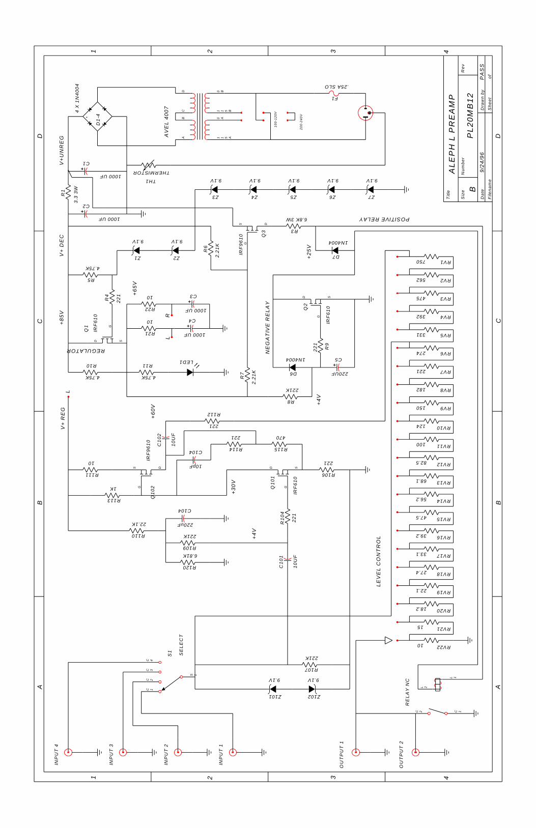
The Aleph L is a simple Mosfet stereo preamplifier having four single-ended inputs andtwo outputs. Its controls consist of an input selector and a level control. The volumecontrol is passive up to the 3:00 o’clock position where the gain is unity. At 3:00o’clock, the connection from input to output is direct, with no components in the signalpath, and past the 3:00 o’clock position the unit becomes an active preamp.
The gain stage of the preamp is a single Mosfet operated common source and biasedby a Mosfet constant current source.
Figure 1 shows the schematic of the preamp, indicating the component designationsand values and various voltages.
The power supply and the left channel are shown. Power supply and componentscommon to both channels have reference designators less than 100. The left channelis 100 to 199, and the right channel is 200 to 299.
The power supply transformer delivers approximately 84 volts (for 120 or 240 VACoperation) unregulated DC into C1, which is then passively filtered and then activelyregulated down to about 60 volts at the output of Q1. Q1 is driven by a stack of Zenerdiodes and the regulated output is additionally filtered by C3 and C4 to form the leftand right supplies.
The output muting relay is controlled by the circuits of Q2 and Q3. For the relay toactivate, both Q2 and Q3 must be conducting. Q3 turns on slowly via the charge onC5, while Q2 will only conduct when there is at least 8 volts difference betweenregulated and unregulated supplies. Thus Q3 delays relay turn on, and Q2 shuts it offquickly.
The audio gain stage consists of Q101. The input goes to the gate, and the outputappears at the drain. Q102 inverts the signal, so the circuit as a whole is non inverting.
The output of the gain stage goes to the level control which is a 23 position steppedattenuator whose wiper is attached to the preamp output.
Fig 2 shows the circuit board layout, with the components identified by designators.
Fig 3 shows the circuit board layout, with the components identified by values.
Fig 4 shows the circuit board layout of the volume control.
Fig 5 shows the Aleph L upgrade.
R106
221
10UF
C102
R11
4.75K
1000 UF
C41000 UF
C310
R22
10
R21
2.21
K
R6
221
R112
TH1THERMISTOR
1 1 5 A
0 A1 1 5 B
0 B
AB
CD
D1-4
4 X
1N40
04
-+
1000 UF
C2
R1
3.3
3W
C1
1000 UF
IRF9
610 Q3
S D
G
6.8K 3W
R3
750 RV1
562 RV2
475 RV3
392 RV4
331 RV5
274 RV6
221 RV7
182 RV8
150 RV9
124 RV10
100 RV11
82.5 RV12
68.1 RV13
56.2 RV14
47.5 RV15
39.2 RV16
33.1 RV17
27.4 RV18
22.1 RV19
18.2 RV20
15 RV21
C 2 C 1
10 RV22
RELA
Y NC L 2
L 1
SELE
CT
S1
S 1
C 3C 2
C 4C 1
R111
10 IRF9
610
Q102
S D
G
R109
221K
C104
220uFIR
F610
Q101
SD
GR1
04
221
C101
10UF
R107
221K
9.1V
Z101
9.1V
Z102
OUTP
UT 2
INPU
T 1
INPU
T 2
INPU
T 3
INPU
T 4
9.1V
Z7
9.1V
Z6
9.1V
Z5
9.1V
Z4
9.1V
Z3
OUTP
UT 1
F1
.25A SLO
221K
R8
2.21
K
R7
Z1
9.1V
Z2
9.1V
IRF6
10Q1
SD
G
221R4
4.75K
R5
C5
220UF
R9221
Q2
IRF6
10G
D S
D6
1N4004R10
4.75K
LED1
D7
1N4004
R120
6.81K
R113
1K
C104
10pF
R115
470
R114
221
R110
22.1K
9/24
/96
LEVE
L CO
NTRO
L
L
LR
+25V
+4V
+30V
V+UN
REG
POSITIVE RELAY
AVEL
400
7
PASS
ALEP
H L
PREA
MP
100-
120V
200-
240V
V+ R
EG +60V
V+ D
EC
+65V
+85V
REGULATOR
NEGA
TIVE
REL
AY
+4V
PL20
MB1
2
AB
CD
4321
DC
BA
1 2 3 4
BRe
vNu
mbe
r
Title
Size
Date
Filen
ame
Draw
n by
ofSh
eet


ALEPH L Update
Rev 1.0 to 1.1
The kit contains one new main board with the correct value for R212, but pleaseverify before doing the conversion.
To update the Aleph L from rev 1.0 to either rev 1.1 is a simple matter ofreplacing the main board, with two minor exceptions.
1. R212 must be 562 ( see attached drawing for location).
2. When keeping the old volume control board the white wire must beattached as shown in the drawing of the old volume board.

SPECIFICATIONS
Gain 17 dB
Freq. Response +0, -3 dB @ 10 Hz and 100 kHz
Distortion < .2 % THD typically .02% @ 1 volt @ 1KHZ
Maximum Output 10 volts rms.
Output Impedance 0 - 750 ohms
Input Impedance 20 Kohm
Output Noise less than 10 microvolts, unweighted 20-20khz
Power Consumption 15 watts
Dimensions 12 " W x 11.5 “ D x 4" H
Shipping Weight 22 lb.
Pass Laboratories24449 Foresthill Rd.
Foresthill CA 95631
tel (530) 367 3690fax (530) 367 2193