Embed Size (px)
Citation preview

Passive Intermodulation at Junctions
Workshop: High Power Issues of Microwave Filter
Design and Realization
Carlos Vicente* & Hans L. Hartnagel†
(Email: [email protected])
* Universidad Politécnica de Valencia† Technische Universität Darmstadt
IMS2007

Outline
• Introduction & Motivation
• PIM Basics
• Theoretical PIM results at Metallic Contacts
• Experimental PIM results at Flanges
• Conclusions & Future Research Directions
2

Introduction
Higher risk of PIM distortion.
Number of carriers increases.
Output power also rises.
Dimensions of the components decrease.
As time goes by:
This leads to:
3

Motivation
Many fundamental aspects of PIM remain unknown.
Extremely difficult to assess quantitatively.
No models exist.
Becomes more important in future missions.
4

PIM Basics
Two separated frequency bands in satellites.
Transmission band: high power.
Reception band: low power.
Tx Rx5

PIM Basics
Two separated frequency bands in satellites.
Transmission band: high power.
Reception band: low power.
Any practical system: Nonlinear:
Tx Rx
I
V
I = a0+a
1V+a
2V2+a
3V3+...
6

PIM Basics
Two separated frequency bands in satellites.
Transmission band: high power.
Reception band: low power.
Any practical system: Nonlinear:
Harmonics and IM products
Tx IM products distort Rx.
Tx RxIM
I
V
fint = mf2+nf1
|m|+|n|=N (PIM order)
I = a0+a
1V+a
2V2+a
3V3+...
7

PIM Basics
➔ PIM phenomena[Foord]:
Tunnelling Thermionic emission Fritting
Fretting
FerromagneticThermalIonizationField emission
Contact phenomena
Noncontact phenomena
8

PIM Basics
PIM sources:
Ferromagnetic materials.
Metallic contacts.
Voids or cracks discharges
Thermal effects
9

PIM Basics
PIM sources:
Ferromagnetic materials.
Metallic contacts.
Voids or cracks discharges
Thermal effects
10

PIM Basics
Metallic Contacts:
Flanges [Cox, Vicente05a]
Tuning screws
Deployable reflector[Scialino]
MEMS [Johnson]
11

PIM Basics
Metallic Contacts:
Flanges
Tuning screws
Deployable reflector
MEMS
THEORY
12
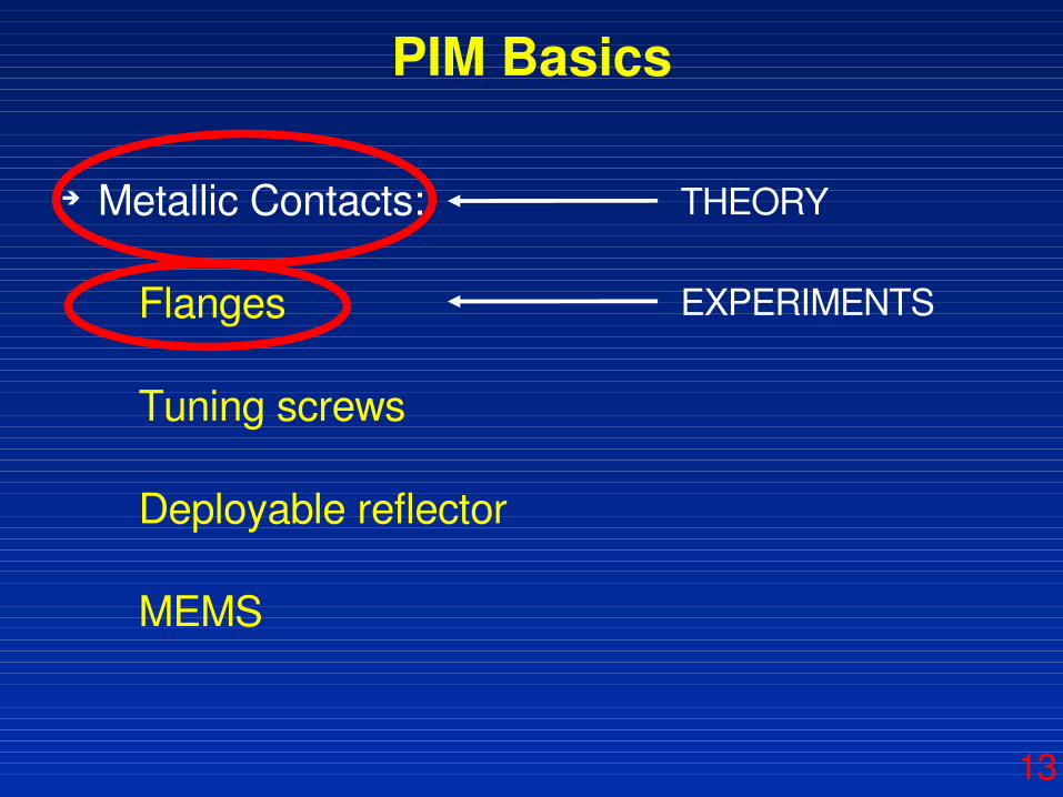
PIM Basics
Metallic Contacts:
Flanges
Tuning screws
Deployable reflector
MEMS
THEORY
EXPERIMENTS
13

PIM at Metallic Contacts
Irregularities reduce the total area of contact.
Contaminant layers on the surface preventthe formation of Ohmic contacts.
METAL A
METAL B
14

PIM at Metallic Contacts [Vicente05b]
Irregularities reduce the total area of contact.
Contaminant layers on the surface preventthe formation of Ohmic contacts.
RC
Cc
Rnlc
Rcons
Rnlnc
Cnc
Equivalent circuit:
METAL A
METAL B
15

Theoretical PIM Results at Metallic Contacts
PIM vs. Hardness
PIM vs. Thickness oxide layer
Hardness PIM:
The softer the material the easier it is deformed,increasing the area of contact and reducing the current density.
Thickness PIM:
If the oxide layer is thin, the contact resistance is lower.
Care: The process can depend on the thickness.(e. g. Tunnelling).
16

Theoretical PIM Results at Metallic Contacts
PIM vs. Roughness
PIM vs. Cracking
Cracking PIM:
The ability to break the oxide layer to form MM contacts has a strong impact in the PIM response.
Roughness PIM:
Impact basically at low contact pressures.
Care: Rougher surfaces can lead to a higher degree of cracking, reducing the PIM level.
17

Theoretical PIM Results at Metallic Contacts
PIM vs. Pressure
PIM vs. Freq.
PIM level trend changes depending on its source.
Two disconnected processes can easily coexist.
High PIM orders lead to more PIM frequencies.
There can be influence of high PIM orders into the lower ones.
Higher PIM level at lower frequencies due to the proximity to the cutoff frequency.
18

PIM vs. Combined Power PIM vs. Power Ratio
PIM vs. Combined power:N dB/dB rule.
• fint = mf2+nf1
• |m|+|n|=N (PIM order)
Theoretical PIM Results at Metallic Contacts
Nm/n
PIM vs. Carrier power ratio: Maximum at: P2 = (m/n)*P1
Slopes: m, n19

PIM vs. Combined Power PIM vs. Power Ratio
● Curves valid if:No higher PIM orders contribute.No change of contact properties.
Theoretical PIM Results at Metallic Contacts
Nm/n
• fint = mf2+nf1
• |m|+|n|=N (PIM order)
20

Theoretical PIM Results PIM Software as a module of ESA/ESTEC FEST3D Software
Courtesy of ESA/ESTEC 21

Experimental PIM Results at Flanges[Vicente07]
Aluminium waveguides and Agplated aluminium waveguides.
• f1 = 11.21 GHz , f2 =11.895 GHz , PIM = 12.58 GHz
• 2x170 W, noise level [145, 150] dBm
Gaskets of different materials: Agplated, Indium, Gold,...
22

Test setup[Wolk]
2x170 W, noise level [145, 150] dBm
23
Courtesy of TesatSpacecom

Test setup Input section
Output section
24

Experimental PIM Results at Flanges Aluminium Waveguides + Al Gasket: 60 W
Aluminium Waveguides + 2 Al Gasket: 60 W Aluminium Waveguides + In Gasket: 60 W
Aluminium Waveguides: 60 W
25

Experimental PIM Results at Flanges Aluminium Waveguides: 4 Ncm
Discrepancy with the N dB/dB rule:
1) Higher order modes?
2) Change of contact properties (increase of Temperature).
Aluminium Waveguides: 80 Ncm
26

Experimental PIM Results at Flanges Aluminium Waveguides: 4 Ncm
Aluminium Waveguides: 4 Ncm: P = 100 W
Aluminium Waveguides: 80 Ncm
Aluminium Waveguides: 4 Ncm: P = 170 W
27

Agplated Waveguides: 340 W
Agplated Waveguides + 2 Ag Gaskets: 340 W
Agplated Waveguides + Ag gasket: 340 W
Experimental PIM Results at Flanges
28
PIM in silver contacts is independent of applied torque (contact pressure).
Only including two gaskets, the PIM level can be driven below the noise level.

Agplated Waveguides: 340 W
Agplated Waveguides + 2 Ag Gaskets: 340 W
Agplated Waveguides + Ag gasket: 340 W
Agplated Waveguides + In Gasket: 340 W
Experimental PIM Results at Flanges
29

Experimental PIM Results at Flanges
Seal of the flanges:
Without gasket With a flat gasket
30

Seal of two plates separated by a single screw[Song]:
rc = BT+LP/2Song et al.
It holds for clean surfaces:
Independent of material properties and applied pressure!!
PIM independent of applied torque!!
rc: radius of contactBT: bolt radiusLP: flange thickness
31
Experimental PIM Results at Flanges

Our application:
Insertion of gaskets Effective increase of flange thickness.
Rule of thumb (conservative?):
Distance between screws lower than 2*rc
DUT flanges do not accomplish such a rule PIM.
Interface flanges do NO PIM.
32
Experimental PIM Results at Flanges

Conclusions & Future Research Directions
• PIM theory at Metallic Contacts presented.
• Significant contribution to PIM at flanges.
• More tests with other configurations.
• Lowweight PIMfree flanges design.
33

Acknowledgements
34
● European Commission:● “Milimetrewave and Microwave Components Design Framework for Ground and Space Multimedia Network, RTN1199900105.
● European Space Agency (ESA):● “Multipactor and Corona discharge: Prediction, Simulation and Design in Microwave Components”, Contract No. 18827/02/NL/EC.
● “Surface Treatment and Coating for the Reduction of Multipactor and Passive Intermodulation (PIM) Effects in RF Components”, Contract No. 17025/03/NL/EC.
● TesatSpacecom GmbH & Co. KG:● For providing the measured data.
Selected References
35
● [Cox] R. D. Cox, “Measurement of Waveguide Component and Joint Mixing Products in 6 GHz Frequency Diversity Systems,” IEEE Transactions on Communication Technology, vol. 18, pp. 3337, 1970.
● [Vicente05a] C. Vicente and H. Hartnagel, “PassiveIntermodulation Analysis Between Rough Rectangular Waveguide Flanges,” IEEE Transactions on Microwave Theory and Techniques, vol. 53, pp. 25152525, August, 2005.
● [Vicente05b] C. Vicente “Passive Intermodulation and Corona Discharge for Microwave Structures in Communications Satellites,” PhD. Thesis, Technical University of Darmstadt, Darmstadt, Germany, 2005.
● [Vicente07] C. Vicente, D. Wolk, H. L. Hartnagel, B. Gimeno, V. Boria and D. Raboso, “Experimental Analysis of Passive Intermodulation at Waveguide Flange Bolted Connections,” to be published in IEEE Transactions on Microwave Theory and Techniques, May, 2007.
● [Wolk] D. Wolk, “Surface Treatment and Coating for the Reduction of Multipactor and Passive Intermodulation (PIM) Effects in RF Components”, Final Report ESA/ESTEC Contract No. 17025/03/NL/EC.

Selected References
36
● [Johnson] J. Johnson, G. G. Adams and N. E.McGruer, “Determination of Intermodulation Distortion in a MEMS Microswitch,” IEEE MTTS International Microwave Symposium Digest 2005.
● [Scialino] G. L. Scialino, V. Lubrano, F. Silvestrucci, E. Fei, A. Cherniavsky, D. Raboso, K. v. 't Klooster, A. Drobishev, K. Vasilyev, “Presentation of Passive Intermodulation activities within the large deployable reflector study,” 5th International Workshop on Multipactor, Corona and Passive Intermodualtion in Space RF Hardware, 1214 Septemeber 2005, ESAESTEC, The Netherlands.
● [Song] S. Song and K. P. Morgan, “Thermal and electrical resistances of bolted joints between plates of unequal thickness,” Semiconductor Thermal Measurement and Management Symposium, 1993, SEMITHERM IX., Ninth Annual IEEE, pp 2834, February 1993