Embed Size (px)
Citation preview
TMS37157
www.ti.com SWRS083A –SEPTEMBER 2009–REVISED NOVEMBER 2009
PASSIVE LOW FREQUENCY INTERFACE DEVICE WITH EEPROMAND 134.2 kHz TRANSPONDER INTERFACE
Check for Samples: TMS37157
1FEATURES APPLICATIONS• Wireless Batteryless Sensor Interface using• Wide Supply Voltage Range 2 V to 3.6 V
Energy Harvesting• Ultra Low Power Consumption– Microcontroller and Sensor can be– Active Mode Max. 150 μA Powered Through the LF Link
– Power Down Mode 60 nA – Data is Directly Transmitted Over the LF• 121 Free Bytes User Memory Link From the Base Station via the
TMS37157 to the Micrcontroller and Vice• Low Frequency Halb Duplex (HDX) InterfaceVersa.– HDX Transponder Communication
• Batteryless Configuration MemoryAchieving Maximum Perfomance and– Memory can be Written Without BatteryHighest Noise Immunity
Support– Special Selective Addressing Mode Allows
– Microcontroller can Read the Content of theAnti CollisionMemory When It Gets Connected to a
– Up to 8 kbit/s LF Uplink Data Rate Battery and Use It for Configuration– 126 Byte EEPROM: – Microcontroller can Write the Memory,
Which can be Read Out Later Through the– 121 Bytes Free Available EEPROM UserLF LinkMemory
• Ultra Low Power Data Logger Memory (Smart– 32 Bit Unique Serial NumberMetering)
– 8 Bit Selective Address– Memory Can Be Written By a
– High EEPROM Flexibility Microcontroller– Pages are Irreversible Lockable and – Memory Can Be Read Through LF Interface
Protectable Without Battery Support– Battery Check and Battery Charge Function • Multi Purpose LF Interface to a Microcontroller
– Short Range RF Interface to a– Resonance Frequency: 134.2 kHzMicrocontroller Where Other Frequencies– Integrated Resonance Frequency Trimmingare Not an Option
– Downlink – Amplitude Shift Keying – Ultra Low Power Mode can Result in an– Uplink – Frequency Shift Keying Overall Power Consumption of 60 nA
• 3 Wire SPI Interface for Accessing the • Remote Control ApplicationEEPROM and Exchanging Data With the – Combination With an UHF Transmitter or IRMicrocontroller Through the LF Interface Transmitter and a μC
• 0.6mm Pitch, 4mm x 4mm VQFN Package – Power Management of the TMS37157 canPower Down the Microcontroller
– The Push Button Detection Circuit canPower Up a Microcontroller
• Stand Alone LF-Transponder with Memory– RFID Transponder with Unique ID and 121
Bytes Free Programmable EEPROM UserMemory
– Only Few Additional Components Needed– No Battery Required
1
Please be aware that an important notice concerning availability, standard warranty, and use in critical applications of TexasInstruments semiconductor products and disclaimers thereto appears at the end of this data sheet.
PRODUCTION DATA information is current as of publication date. Copyright © 2009, Texas Instruments IncorporatedProducts conform to specifications per the terms of the TexasInstruments standard warranty. Production processing does notnecessarily include testing of all parameters.
LF Reader
134,2 kHzTMS37157
Microcontroller
LF DATA
ENERGY
Base Station Sensor System
Digital or Analog
Sensor
TMS37157
SWRS083A –SEPTEMBER 2009–REVISED NOVEMBER 2009 www.ti.com
DESCRIPTION/ORDERING INFORMATIONThe TMS37157 combines a Low Frequency Transponder Interface with an SPI Interface and PowerManagement for a connected microcontroller. It is the ideal device for any Configuration, Data Logger-, Sensor-or Remote Control Application. The Transponder memory is accessible through SPI and LF and, in the secondcase, operates without the need for a battery. The use of the Low Frequency Band ensures a communication ina defined direction and harsh environments.
The TMS37157 manages the Transponder communication and push button interaction. During sleep state thedevices enters a special low power mode with only 60 nA current consumption.
The EEPROM memory is accessible over the LF interface without support from the battery or through SPI by amicrocontroller if a battery is connected. The TMS37157 offers a special battery charge mode.
The external resonance circuit with a LF coil and a resonance capacitor can be trimmed to the correct resonancefrequency with the integrated trimming capability achieving an easy way to eliminate part tolerances.
The small RSA 16-pin package together with only a few external components results in a cost efficient design.
2 Submit Documentation Feedback Copyright © 2009, Texas Instruments Incorporated
Product Folder Link(s): TMS37157
1
16 15 14 13
12
11
10
9
8765
4
3
2
RF1
TCLK
TDAT
TEN
EO
B
PU
SH
BU
SY
CLK_AM
SPI_CLK
SPI_SIMO
VB
AT
I
VB
AT
GN
D
VC
L
NP
OR
SPI_SOMI
TMS37157
www.ti.com SWRS083A –SEPTEMBER 2009–REVISED NOVEMBER 2009
PIN CONFIGURATION
TERMINAL FUNCTIONSTERMINAL
I/O DESCRIPTIONNAME NO.
RF1 1 I Antenna
Test interface - clock input. Data is shifted in and out of the TDAT pin on the rising edge ofTCLK 2 I TCLK.
TDAT 3 I/O Test interface – bidirectional serial data I/O for configuration and trimming.
TEN 4 I Test interface – enable input.
EOB 5 O End of burst detector. This signal is high when the RF signal of the base station is OFF.
NPOR 6 O Active low power-on-reset (open drain) - can be used to reset the microcontroller.
PUSH 7 I Input of the push button detector – can be used to recognize that a push event has occurred.
Indicates internal control unit activity:• During initialization
BUSY 8 O• During transponder operation• During SPI communication (handshaking)
This output provides clock signals derived from the external antenna resonance circuit to theCLKA_M 9 O microcontroller. This function can be activated by an SPI command. Two frequencies are
selectable FRES and FRES/4.
SPI_CLK 10 I SPI clock input
SPI_SOMI 11 O SPI data output
SPI_SIMO 12 I SPI data input
VBATI 13 PWR Can be used as μC supply voltage
VBAT 14 PWR Battery supply
GND 15 PWR Ground
VCL 16 PWR Charge capacitor
ORDERING INFORMATIONTA PACKAGE (1) (2) ORDERABLE PART NUMBER TOPSIDE MARKING
–40°C to 85°C VQFN – RSA Reel of 3000 TMS37157IRSARG4 37157I
(1) Package drawings, thermal data, and symbolization are available at www.ti.com/packaging.(2) For the most current package and ordering information, see the Package Option Addendum at the end of this document, or see the TI
website at www.ti.com.
Copyright © 2009, Texas Instruments Incorporated Submit Documentation Feedback 3
Product Folder Link(s): TMS37157
TMS37157
SWRS083A –SEPTEMBER 2009–REVISED NOVEMBER 2009 www.ti.com
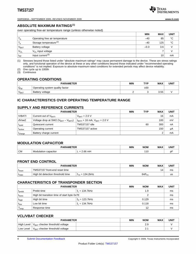
ABSOLUTE MAXIMUM RATINGS (1)
over operating free-air temperature range (unless otherwise noted)MIN MAX UNIT
TA Operating free air temperature –40 85 °C
Ts Storage temperature (2) –40 125 °C
VBAT Battery voltage –0.3 3.6 V
VCL VCL input voltage 7 V
IRF Input current (3) 10 mA
(1) Stresses beyond those listed under "absolute maximum ratings" may cause permanent damage to the device. These are stress ratingsonly, and functional operation of the device at these or any other conditions beyond those indicated under "recommended operatingconditions" is not implied. Exposure to absolute-maximum-rated conditions for extended periods may affect device reliability.
(2) One cycle up to 1000h(3) Continuous
OPERATING CONDITIONSPARAMETER MIN TYP MAX UNIT
Qop Operating system quality factor ≥30
VBAT Battery voltage 2 3 3.55 V
IC CHARACTERISTICS OVER OPERATING TEMPERATURE RANGE
SUPPLY AND REFERENCE CURRENTSPARAMETER MIN TYP MAX UNIT
IVBATI Current out of VBATI VBAT = 2.0 V 16 mA
dVsw2 Voltage drop at SW2 (VBAT – VBATI) IBATI = 16 mA, VBAT = 2.0 V 100 mV
Iquiet Quiescent current TMS37157 idle 60 300 nA
Iactive Operating current TMS37157 active 150 μA
Icharge Battery charge current 2 mA
MODULATION CAPACITORPARAMETER MIN NOM MAX UNIT
CM Modulation capacitor L = 2.66 mH 110 pF
FRONT END CONTROLPARAMETER MIN NOM MAX UNIT
treset TMS37157 front-end reset time 14 ms
tHdet High bit detection threshold time fTX = 134.2kHz 64/fTX us
CHARACTERISTICS OF TRANSPONDER SECTIONPARAMETER MIN NOM MAX UNIT
tprebit Prebit time fL = 134.7kHz 1.9 ms
ttrans High bit transition time of start byte 0x7E 2 ms
thigh High bit time fH = 123.7kHz 0.129 ms
tlow Low bit time fL = 134.7kHz 0.118 ms
Tresp Response time 12 ms
VCL/VBAT CHECKERPARAMETER MIN NOM MAX UNIT
High Level VBAT checker threshold voltage 2.9 V
Low Level VBAT checker threshold voltage 2.1 V
4 Submit Documentation Feedback Copyright © 2009, Texas Instruments Incorporated
Product Folder Link(s): TMS37157
TMS37157
www.ti.com SWRS083A –SEPTEMBER 2009–REVISED NOVEMBER 2009
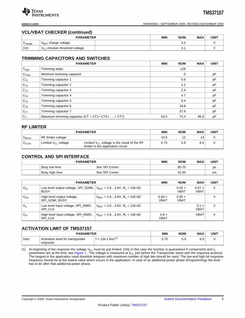
VCL/VBAT CHECKER (continued)PARAMETER MIN NOM MAX UNIT
Vcharge VBAT charge voltage 3.4 V
Vch VCL checker threshold voltage 3.1 V
TRIMMING CAPACITORS AND SWITCHESPARAMETER MIN NOM MAX UNIT
Tstep Trimming steps 128
CTmin Minimum trimming capacitor 0 pF
CT1 Trimming capacitor 1 0.6 pF
CT2 Trimming capacitor 2 1.2 pF
CT3 Trimming capacitor 3 2.4 pF
CT4 Trimming capacitor 4 4.7 pF
CT5 Trimming capacitor 5 9.4 pF
CT6 Trimming capacitor 6 18.8 pF
CT7 Trimming capacitor 7 37.6 pF
CT Maximum trimming capacitor (CT = CT1+ CT2+ … + CT7) 63.5 74.4 85.9 pF
RF LIMITERPARAMETER MIN NOM MAX UNIT
VRFlim RF limiter voltage 10.5 12 14 V
VCLlim Limited VCL voltage Limited VCL voltage is the result of the RF 5.75 5.9 6.5 Vlimiter in the application circuit
CONTROL AND SPI INTERFACEPARAMETER MIN NOM MAX UNIT
Busy low time See SPI Comm. 30-70 μs
Busy high time See SPI Comm. 10-30 ms
PARAMETER MIN NOM MAX UNIT
VOL Low level output voltage, SPI_SOMI, VBAT = 2.0…3.6V, RL = 100 kΩ 0.05 × 0.07 × VBUSY VBAT VBAT
VOH High level output voltage, VBAT = 2.0…3.6V, RL = 100 kΩ 0.93 × 0.95 × VSPI_SOMI, BUSY VBAT VBAT
VIL Low level input voltage, SPI_SIMO, VBAT = 2.0…3.6V, RL = 100 kΩ 0.1 × VSPI_CLK VBAT
VIH High level input voltage, SPI_SIMO, VBAT = 2.0…3.6V, RL = 100 kΩ 0.9 × VBAT VSPI_CLK VBAT
ACTIVATION LIMIT OF TMS37157PARAMETER MIN NOM MAX UNIT
Vact Activation level for transponder f = 134.2 kHz (1) 5.75 5.9 6.5 Vresponse
(1) At beginning of the response the voltage VCL must be just limited. Only in this case the function is guaranteed if components and ICparameters are at the limit, see Figure 1 . The voltage is measured at VCL just before the Transponder starts with the response protocol.The longest in the application used downlink telegram with maximum number of high bits should be used. The low and high bit responsefrequency should be at the lowest value which occurs in the application. In case of an additional power phase (Programming) the levelhas to be after that additional power phase.
Copyright © 2009, Texas Instruments Incorporated Submit Documentation Feedback 5
Product Folder Link(s): TMS37157
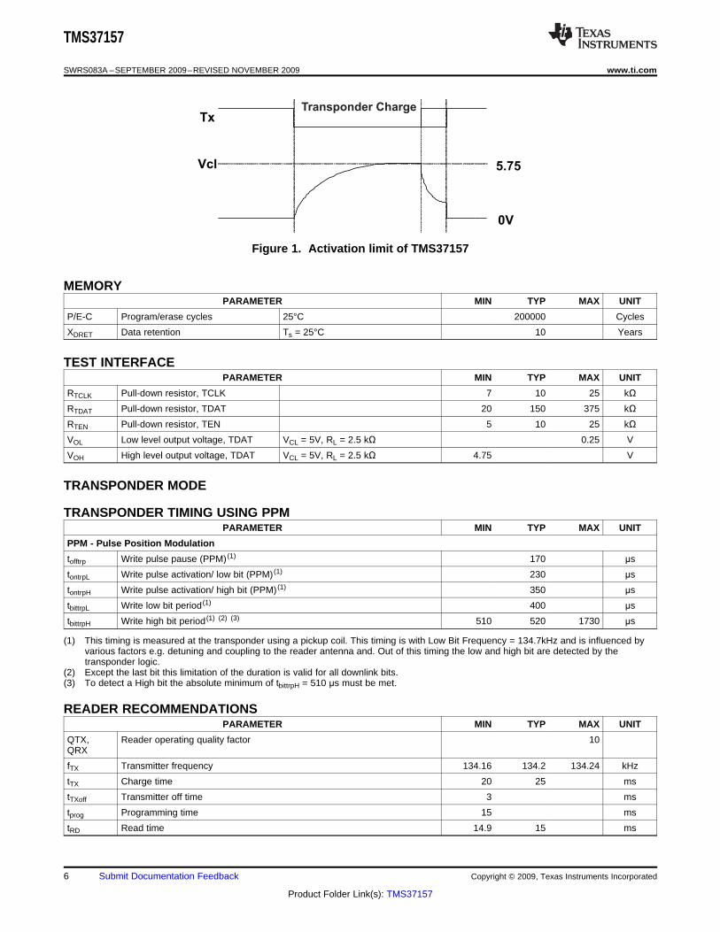
0V
5.75
Tx
Vcl
Transponder Charge
TMS37157
SWRS083A –SEPTEMBER 2009–REVISED NOVEMBER 2009 www.ti.com
Figure 1. Activation limit of TMS37157
MEMORYPARAMETER MIN TYP MAX UNIT
P/E-C Program/erase cycles 25°C 200000 Cycles
XDRET Data retention Ts = 25°C 10 Years
TEST INTERFACEPARAMETER MIN TYP MAX UNIT
RTCLK Pull-down resistor, TCLK 7 10 25 kΩRTDAT Pull-down resistor, TDAT 20 150 375 kΩRTEN Pull-down resistor, TEN 5 10 25 kΩVOL Low level output voltage, TDAT VCL = 5V, RL = 2.5 kΩ 0.25 V
VOH High level output voltage, TDAT VCL = 5V, RL = 2.5 kΩ 4.75 V
TRANSPONDER MODE
TRANSPONDER TIMING USING PPMPARAMETER MIN TYP MAX UNIT
PPM - Pulse Position Modulation
tofftrp Write pulse pause (PPM) (1) 170 μs
tontrpL Write pulse activation/ low bit (PPM) (1) 230 μs
tontrpH Write pulse activation/ high bit (PPM) (1) 350 μs
tbittrpL Write low bit period (1) 400 μs
tbittrpH Write high bit period (1) (2) (3) 510 520 1730 μs
(1) This timing is measured at the transponder using a pickup coil. This timing is with Low Bit Frequency = 134.7kHz and is influenced byvarious factors e.g. detuning and coupling to the reader antenna and. Out of this timing the low and high bit are detected by thetransponder logic.
(2) Except the last bit this limitation of the duration is valid for all downlink bits.(3) To detect a High bit the absolute minimum of tbittrpH = 510 μs must be met.
READER RECOMMENDATIONSPARAMETER MIN TYP MAX UNIT
QTX, Reader operating quality factor 10QRX
fTX Transmitter frequency 134.16 134.2 134.24 kHz
tTX Charge time 20 25 ms
tTXoff Transmitter off time 3 ms
tprog Programming time 15 ms
tRD Read time 14.9 15 ms
6 Submit Documentation Feedback Copyright © 2009, Texas Instruments Incorporated
Product Folder Link(s): TMS37157
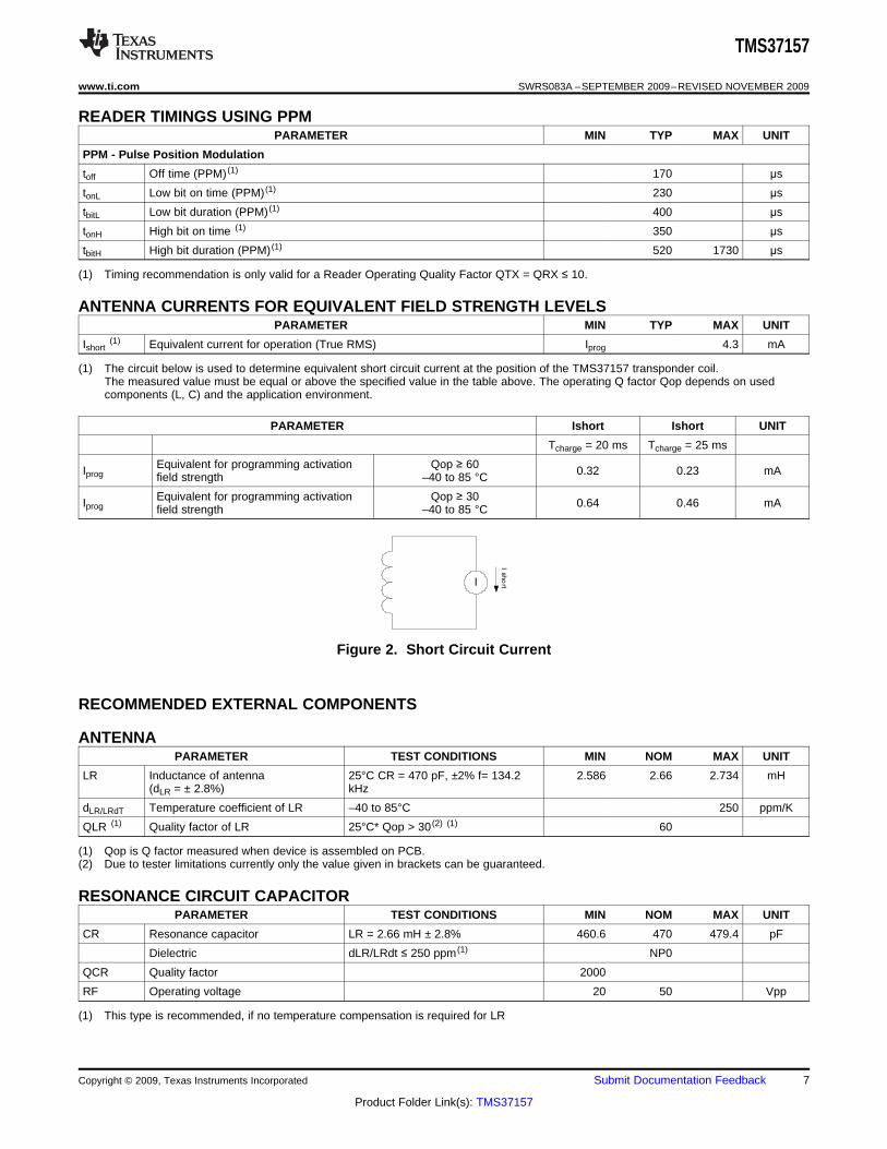
I
Isho
rt
TMS37157
www.ti.com SWRS083A –SEPTEMBER 2009–REVISED NOVEMBER 2009
READER TIMINGS USING PPMPARAMETER MIN TYP MAX UNIT
PPM - Pulse Position Modulation
toff Off time (PPM) (1) 170 μs
tonL Low bit on time (PPM) (1) 230 μs
tbitL Low bit duration (PPM) (1) 400 μs
tonH High bit on time (1) 350 μs
tbitH High bit duration (PPM) (1) 520 1730 μs
(1) Timing recommendation is only valid for a Reader Operating Quality Factor QTX = QRX ≤ 10.
ANTENNA CURRENTS FOR EQUIVALENT FIELD STRENGTH LEVELSPARAMETER MIN TYP MAX UNIT
Ishort(1) Equivalent current for operation (True RMS) Iprog 4.3 mA
(1) The circuit below is used to determine equivalent short circuit current at the position of the TMS37157 transponder coil.The measured value must be equal or above the specified value in the table above. The operating Q factor Qop depends on usedcomponents (L, C) and the application environment.
PARAMETER Ishort Ishort UNIT
Tcharge = 20 ms Tcharge = 25 ms
Equivalent for programming activation Qop ≥ 60Iprog 0.32 0.23 mAfield strength –40 to 85 °C
Equivalent for programming activation Qop ≥ 30Iprog 0.64 0.46 mAfield strength –40 to 85 °C
Figure 2. Short Circuit Current
RECOMMENDED EXTERNAL COMPONENTS
ANTENNAPARAMETER TEST CONDITIONS MIN NOM MAX UNIT
LR Inductance of antenna 25°C CR = 470 pF, ±2% f= 134.2 2.586 2.66 2.734 mH(dLR = ± 2.8%) kHz
dLR/LRdT Temperature coefficient of LR –40 to 85°C 250 ppm/K
QLR (1) Quality factor of LR 25°C* Qop > 30 (2) (1) 60
(1) Qop is Q factor measured when device is assembled on PCB.(2) Due to tester limitations currently only the value given in brackets can be guaranteed.
RESONANCE CIRCUIT CAPACITORPARAMETER TEST CONDITIONS MIN NOM MAX UNIT
CR Resonance capacitor LR = 2.66 mH ± 2.8% 460.6 470 479.4 pF
Dielectric dLR/LRdt ≤ 250 ppm (1) NP0
QCR Quality factor 2000
RF Operating voltage 20 50 Vpp
(1) This type is recommended, if no temperature compensation is required for LR
Copyright © 2009, Texas Instruments Incorporated Submit Documentation Feedback 7
Product Folder Link(s): TMS37157
ANALOG
FRONT END
POWER
MANAGEMENT
CONTROL
UNIT
TE
N
TD
AT
TC
LK
RF1
VCL
GND
PUSH
TANSPONDER & USER
MEMORY
BU
SY
CL
KA
/M
VBAT
VBATI
NPOR
EO
B
SPI_SIMO
SPI_SOMI
SPI_CLK
TMS37157
SWRS083A –SEPTEMBER 2009–REVISED NOVEMBER 2009 www.ti.com
CHARGE CAPACITORPARAMETER TEST CONDITIONS MIN TYP MAX UNIT
25°C 198 220 242 nFCL Charge capacitor fmeas = 1 kHz
CLdiel Dielectric of CL X7R
VCL Operating voltage 16 Vdc
OTHER COMPONENTSPARAMETER TEST CONDITIONS MIN NOM MAX UNIT
RVCL VCL resistor Depends on application circuit 1 MΩRload VBATI load resistor Depends on application circuit 100 kΩCBAT Battery capacitor 100 nF
CBATI BATI capacitor 100 nF
RECOMMENDED TEST INTERFACE PARAMETERSPARAMETER MIN NOM MAX UNIT
VCL Supply voltage for trim/test 5 V
VIH High level input voltage, TDAT, TCLK & TEN 0.9 × VCL 1.1 × VCL V
VIL Low level input voltage, TDAT, TCLK & TEN 0 0.1 × VCL V
fTclk Clock frequency TCLK 134 kHz
tr, tf Rise and fall time, TDAT, TCLK, TEN 50 ns
tTclkl Test clock low time 3.7 μs
tTclkh Test clock high time 3.7 μs
tTres Test reset time 14 ms
tTrc Test reset to clock time 1 μs
tTds Test data setup time 1 μs
tTdh Test data hold time 1 μs
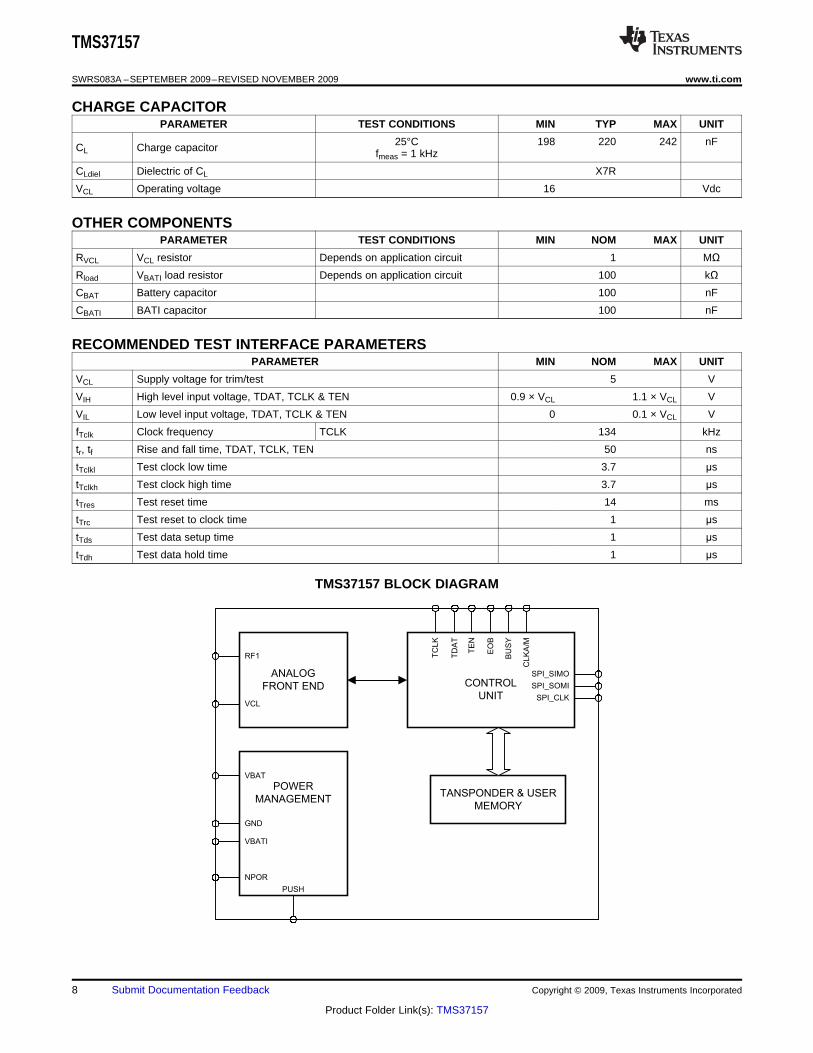
TMS37157 BLOCK DIAGRAM
8 Submit Documentation Feedback Copyright © 2009, Texas Instruments Incorporated
Product Folder Link(s): TMS37157
TMS37157
www.ti.com SWRS083A –SEPTEMBER 2009–REVISED NOVEMBER 2009
BLOCK DESCRIPTION
Analog Front End
The Analog Front End implements all of the analog functions needed to support the TMS37157 transponderfunctions. It enables reception and transmission of LF signals when the transponder is active, and rectifiesincoming LF energy and stores it in an external charge capacitor, to power the device.
The Analog Front End also contains the capacitor array used to trim the transponder's resonance circuit and aclock regenerator function, which is able to recover the clock from an incoming signal so it can be used by thetransponder functions.
Control Unit
DST Transponder
The transponder implemented in the TMS37157 is compatible with Texas Instruments' DST ("Digital SignatureTransponder") transponder. In addition the TMS37157 provides additional Memory for customer use.
CRC Calculation
A hardware cyclic redudancy check calculation engine is implemented in the Control Unit to provide errordetection.
Memory Access
The Control Unit interfaces to the on-chip EEPROM. During power-up, the Control Unit reads the configurationparameters stored in the EEPROM and initializes the TMS37157 circuitry accordingly, and at various timesduring device operation it can read EEPROM data and provide it, for example, to a microcontroller.
SPI Interface
The Control Unit provides an SPI interface that allows it to communicate with a microcontroller. Via this interface,for example, the microcontroller is able to access the contents of the TMS37157 EEPROM.
Test Interface
The Control Unit provides a test interface that allows customers to trim the LF antenna's resonance circuit.
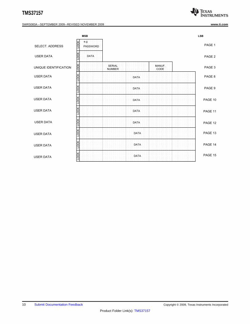
Transponder and User Memory
The Transponder Memory comprises a total of 126 bytes, organized in pages. Memory space is apportioned asfollows:• User Data 121 bytes• Serial Number + Manufactorer Code 4 bytes• Selective Address 1 byte
Copyright © 2009, Texas Instruments Incorporated Submit Documentation Feedback 9
Product Folder Link(s): TMS37157
LSBMSB
UNIQUE IDENTIFICATION
SELECT. ADDRESS
DATAUSER DATA
e.g
.PASSWORDL
OC
KLO
CK
LO
CK
PAGE 1
PAGE 2
PAGE 3SERIAL
NUMBER
MANUF.
CODE
USER DATA
USER DATA
USER DATA
USER DATA
USER DATA
LO
CK
LO
CK
LO
CK
LO
CK
LO
CKPAGE 8
PAGE 9
PAGE 10
PAGE 11
PAGE 12
DATA
LO
CK
DATA
LO
CK
DATA
LO
CK
PAGE 13
PAGE 14
PAGE 15
USER DATA
USER DATA
USER DATA
DATA
DATA
DATA
DATA
DATA
TMS37157
SWRS083A –SEPTEMBER 2009–REVISED NOVEMBER 2009 www.ti.com
10 Submit Documentation Feedback Copyright © 2009, Texas Instruments Incorporated
Product Folder Link(s): TMS37157
1LSBMSB
USER DATA
LO
CK
403224168
LO
CK
LO
CK
LO
CK
LO
CK
LO
CK
LO
CK
LO
CK
PAGE 46
PAGE 47
PAGE 48
DATA
DATA
LO
CK
DATA
LO
CK
DATA
LO
CK
PAGE 49
PAGE 50
PAGE 51
DATA
DATA
DATA
DATA
DATA
DATA
LO
CK
DATAUSER DATA
USER DATA
USER DATA
USER DATA
USER DATA
USER DATA
USER DATA
USER DATA
USER DATA
USER DATA
USER DATA
DATA
LO
CK
PAGE 52
DATA
LO
CK
DATA
LO
CK
DATA
LO
CK
PAGE 53
PAGE 54
PAGE 55
DATAUSER DATA
USER DATA
USER DATA
USER DATA
PAGE 40
PAGE 41
PAGE 42
PAGE 43
PAGE 44
PAGE 45
TMS37157
www.ti.com SWRS083A –SEPTEMBER 2009–REVISED NOVEMBER 2009
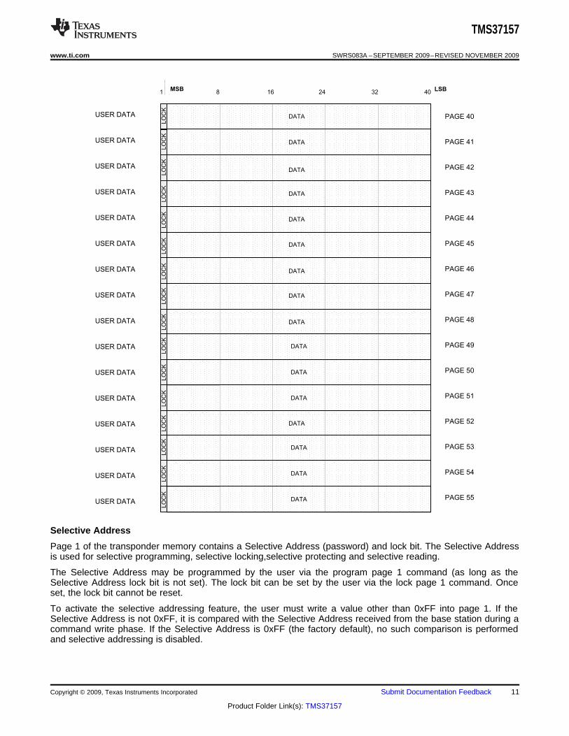
Selective Address
Page 1 of the transponder memory contains a Selective Address (password) and lock bit. The Selective Addressis used for selective programming, selective locking,selective protecting and selective reading.
The Selective Address may be programmed by the user via the program page 1 command (as long as theSelective Address lock bit is not set). The lock bit can be set by the user via the lock page 1 command. Onceset, the lock bit cannot be reset.
To activate the selective addressing feature, the user must write a value other than 0xFF into page 1. If theSelective Address is not 0xFF, it is compared with the Selective Address received from the base station during acommand write phase. If the Selective Address is 0xFF (the factory default), no such comparison is performedand selective addressing is disabled.
Copyright © 2009, Texas Instruments Incorporated Submit Documentation Feedback 11
Product Folder Link(s): TMS37157
TMS37157
SWRS083A –SEPTEMBER 2009–REVISED NOVEMBER 2009 www.ti.com
Whenever pages 1, 2 or 3 are accessed, the Selective Address (from page 1) is returned in the correspondingread phase, together with page 2 and the Manufacturer Code and Serial Number (from page 3). The status of thepage 1 lock bit (1=locked) is only returned when page 1 is accessed.
Page 2
Page 2 of the transponder memory contains 8 bits of user data and lock bit.
Page 2 is typically used for numbering keys in an application (e.g. the key number), it can also be used so savethe value of the trim capacitor array or for anything else. It may be programmed by the user using the programpage 2 command (as long as the lock bit is not set). The lock bit can be set by the user via the lock page 2command. Once set, the lock bit cannot be reset.
Whenever pages 1, 2 or 3 are accessed, page 2 is returned in the corresponding read phase, together with theSelective Address (from page 1) and the Manufacturer Code and Serial Number (from page 3). The status of thepage 2 lock bit (1=locked) is only returned when page 2 is accessed.
Unique Identification
Page 3 of the transponder memory contains an 8-bit Manufacturer Code and a 24-bit Serial Number. TheManufacturer Code and Serial Number are programmed and locked during manufacture and cannot be changed.
The Manufacturer Code is used to distinguish between different devices, the Manufacturer Code of theTMS37157 is 0x0E. The Serial Number is unique for every single TMS37157 device.
Whenever pages 1, 2 or 3 are accessed, the Manufacturer Code and Serial Number (from page 3) are returnedin the corresponding read phase, together with the Selective Address (from page 1) and page 2. The status ofthe page 3 lock bit (1=locked) is only returned when page 3 is accessed.
User Data
The Transponder Memory provides the Pages 2, 8 to 15 and 40 to 55 for data storage. This memory is availableto store any data defined by the user or application.
12 Submit Documentation Feedback Copyright © 2009, Texas Instruments Incorporated
Product Folder Link(s): TMS37157
TMS37157 EEPROM ROMCRC
GEN.
CONTROL
UNIT
TRPINTF.
VOLT.REG.
Q CL
CLEAR
LR
CR
RF
VCL
GND
CL
CHARGEREG. S
P
I
RVCL
SW5
S
VBAT
VBAT
BAT CBAT
PUSH
+
I
BATBATI
VBATION
VBATI
CBATI RVBATI
VCCDBUSY
SPI_CLK
SOMI
SIMOVBATI
CLKA/M
TMS37157
www.ti.com SWRS083A –SEPTEMBER 2009–REVISED NOVEMBER 2009
POWER MANAGEMENT
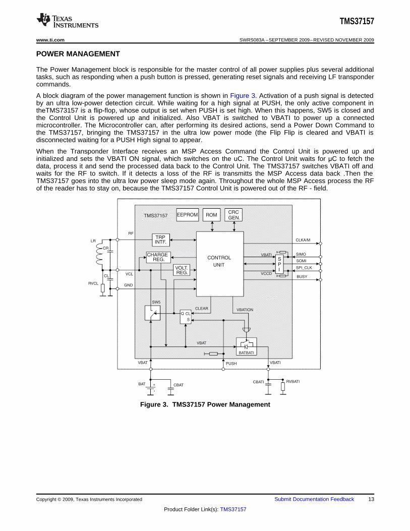
The Power Management block is responsible for the master control of all power supplies plus several additionaltasks, such as responding when a push button is pressed, generating reset signals and receiving LF transpondercommands.
A block diagram of the power management function is shown in Figure 3. Activation of a push signal is detectedby an ultra low-power detection circuit. While waiting for a high signal at PUSH, the only active component intheTMS73157 is a flip-flop, whose output is set when PUSH is set high. When this happens, SW5 is closed andthe Control Unit is powered up and initialized. Also VBAT is switched to VBATI to power up a connectedmicrocontroller. The Microcontroller can, after performing its desired actions, send a Power Down Command tothe TMS37157, bringing the TMS37157 in the ultra low power mode (the Flip Flip is cleared and VBATI isdisconnected waiting for a PUSH High signal to appear.
When the Transponder Interface receives an MSP Access Command the Control Unit is powered up andinitialized and sets the VBATI ON signal, which switches on the uC. The Control Unit waits for μC to fetch thedata, process it and send the processed data back to the Control Unit. The TMS37157 switches VBATI off andwaits for the RF to switch. If it detects a loss of the RF is transmitts the MSP Access data back .Then theTMS37157 goes into the ultra low power sleep mode again. Throughout the whole MSP Access process the RFof the reader has to stay on, because the TMS37157 Control Unit is powered out of the RF - field.
Figure 3. TMS37157 Power Management
Copyright © 2009, Texas Instruments Incorporated Submit Documentation Feedback 13
Product Folder Link(s): TMS37157
TMS37157
SWRS083A –SEPTEMBER 2009–REVISED NOVEMBER 2009 www.ti.com
ADRESSING OF THE TRANSPONDER
The addressing mode of the TMS37157 is defined by the content of page 1.
General Addressing Page 1 = 0xFF
Selective Addressing Page 1 <> 0xFF
Standard configuration is General Addressing. Selective Addressing is activated by programming a value otherthan 0xFF into page 1 of the TMS37157 EEPROM. Selective Addressing affects the Lock Page, Protect Page(not available for Page 1-3) and Program Page commands for page 1 to page 15 and page 40 to page 55. Herethe selective address has to be added to the Command. A Read Page of page 1 – 3 always gives back theselective address.
A General Read is still possible on all pages. For page 1 – 3 a selective read be can done.
To switch off Selective Addressing a selective program page 1 Command with User Data 0xFF has to be send tothe TMS37157.
USE OF THE LOCK BIT
All pages can be locked by setting the corresponding lock bit. Locked pages can not be reprogrammed anymore.The Lock is irreversible.
USE OF THE PROTECTION BIT
Pages 8-15 and 40-55 can be protected by setting the corresponding Protection Bit. Protected pages can only berepgrammed via SPI. The TMS37157 will not answer to a program command on a protected page. General andSelective Read commands are still possible on protected pages. The protection is irreversible.
14 Submit Documentation Feedback Copyright © 2009, Texas Instruments Incorporated
Product Folder Link(s): TMS37157
TMS37157
www.ti.com SWRS083A –SEPTEMBER 2009–REVISED NOVEMBER 2009
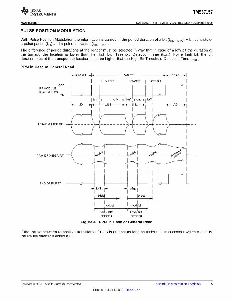
PULSE POSITION MODULATION
With Pulse Position Modulation the information is carried in the period duration of a bit (tbitL, tbitH). A bit consists ofa pulse pause (toff) and a pulse activation (tonL, tonH).
The difference of period durations at the reader must be selected in way that in case of a low bit the duration atthe transponder location is lower than the High Bit Threshold Detection Time (tHdet). For a high bit, the bitduration mus at the transponder location must be higher that the High Bit Threshold Detection Time (tHdet).
PPM in Case of General Read
Figure 4. PPM in Case of General Read
If the Pause between to positive transitions of EOB is at least as long as tHdet the Transponder writes a one. Isthe Pause shorter it writes a 0.
Copyright © 2009, Texas Instruments Incorporated Submit Documentation Feedback 15
Product Folder Link(s): TMS37157
TMS37157
SWRS083A –SEPTEMBER 2009–REVISED NOVEMBER 2009 www.ti.com
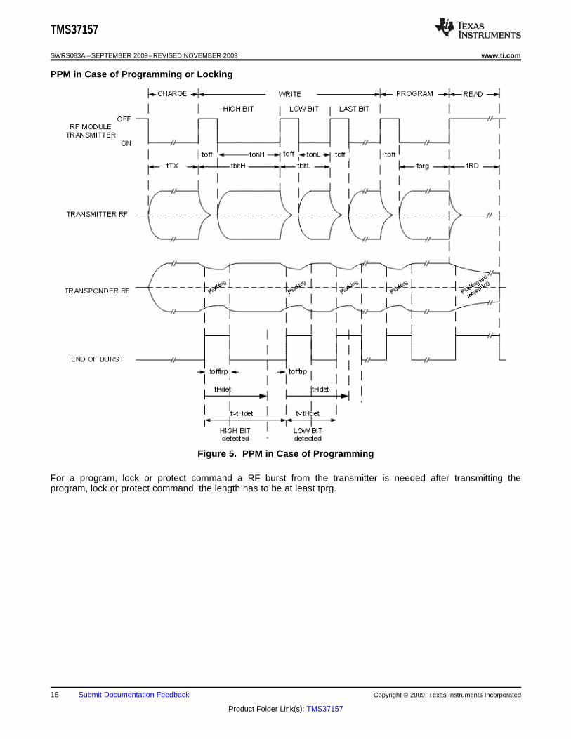
PPM in Case of Programming or Locking
Figure 5. PPM in Case of Programming
For a program, lock or protect command a RF burst from the transmitter is needed after transmitting theprogram, lock or protect command, the length has to be at least tprg.
16 Submit Documentation Feedback Copyright © 2009, Texas Instruments Incorporated
Product Folder Link(s): TMS37157
TMS37157
www.ti.com SWRS083A –SEPTEMBER 2009–REVISED NOVEMBER 2009
TMS37157 COMMANDS
This chapter describes the commands and data that can be transferred to and from the TMS37157 via its contactless LF interface, SPI and Test interfaces.
When communicating with the transponder following naming conventions are used:• Data Transmission from the base station to the transponder is called “write” and “write data are transferred”.• Data Transmission from the transponder to the base station is called “read” and “read data re transferred”.
This is applied independently from the command that is executes whether it is a read, write, program orauthentication function.
Write Formats
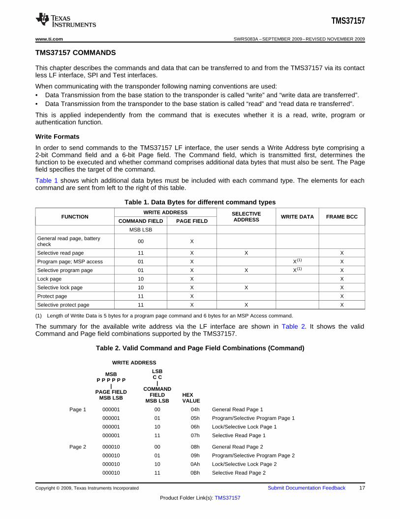
In order to send commands to the TMS37157 LF interface, the user sends a Write Address byte comprising a2-bit Command field and a 6-bit Page field. The Command field, which is transmitted first, determines thefunction to be executed and whether command comprises additional data bytes that must also be sent. The Pagefield specifies the target of the command.
Table 1 shows which additional data bytes must be included with each command type. The elements for eachcommand are sent from left to the right of this table.
Table 1. Data Bytes for different command types
WRITE ADDRESS SELECTIVEFUNCTION WRITE DATA FRAME BCCADDRESSCOMMAND FIELD PAGE FIELD
MSB LSB
General read page, battery 00 Xcheck
Selective read page 11 X X X
Program page; MSP access 01 X X (1) X
Selective program page 01 X X X (1) X
Lock page 10 X X
Selective lock page 10 X X X
Protect page 11 X X
Selective protect page 11 X X X
(1) Length of Wrtite Data is 5 bytes for a program page command and 6 bytes for an MSP Access command.
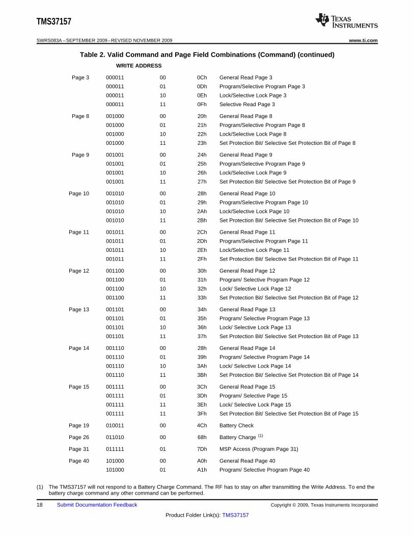
The summary for the available write address via the LF interface are shown in Table 2. It shows the validCommand and Page field combinations supported by the TMS37157.
Table 2. Valid Command and Page Field Combinations (Command)
WRITE ADDRESS
LSBMSB C CP P P P P P || COMMANDPAGE FIELD FIELD HEXMSB LSB MSB LSB VALUE
Page 1 000001 00 04h General Read Page 1
000001 01 05h Program/Selective Program Page 1
000001 10 06h Lock/Selective Lock Page 1
000001 11 07h Selective Read Page 1
Page 2 000010 00 08h General Read Page 2
000010 01 09h Program/Selective Program Page 2
000010 10 0Ah Lock/Selective Lock Page 2
000010 11 0Bh Selective Read Page 2
Copyright © 2009, Texas Instruments Incorporated Submit Documentation Feedback 17
Product Folder Link(s): TMS37157
TMS37157
SWRS083A –SEPTEMBER 2009–REVISED NOVEMBER 2009 www.ti.com
Table 2. Valid Command and Page Field Combinations (Command) (continued)
WRITE ADDRESS
Page 3 000011 00 0Ch General Read Page 3
000011 01 0Dh Program/Selective Program Page 3
000011 10 0Eh Lock/Selective Lock Page 3
000011 11 0Fh Selective Read Page 3
Page 8 001000 00 20h General Read Page 8
001000 01 21h Program/Selective Program Page 8
001000 10 22h Lock/Selective Lock Page 8
001000 11 23h Set Protection Bit/ Selective Set Protection Bit of Page 8
Page 9 001001 00 24h General Read Page 9
001001 01 25h Program/Selective Program Page 9
001001 10 26h Lock/Selective Lock Page 9
001001 11 27h Set Protection Bit/ Selective Set Protection Bit of Page 9
Page 10 001010 00 28h General Read Page 10
001010 01 29h Program/Selective Program Page 10
001010 10 2Ah Lock/Selective Lock Page 10
001010 11 2Bh Set Protection Bit/ Selective Set Protection Bit of Page 10
Page 11 001011 00 2Ch General Read Page 11
001011 01 2Dh Program/Selective Program Page 11
001011 10 2Eh Lock/Selective Lock Page 11
001011 11 2Fh Set Protection Bit/ Selective Set Protection Bit of Page 11
Page 12 001100 00 30h General Read Page 12
001100 01 31h Program/ Selective Program Page 12
001100 10 32h Lock/ Selective Lock Page 12
001100 11 33h Set Protection Bit/ Selective Set Protection Bit of Page 12
Page 13 001101 00 34h General Read Page 13
001101 01 35h Program/ Selective Program Page 13
001101 10 36h Lock/ Selective Lock Page 13
001101 11 37h Set Protection Bit/ Selective Set Protection Bit of Page 13
Page 14 001110 00 28h General Read Page 14
001110 01 39h Program/ Selective Program Page 14
001110 10 3Ah Lock/ Selective Lock Page 14
001110 11 3Bh Set Protection Bit/ Selective Set Protection Bit of Page 14
Page 15 001111 00 3Ch General Read Page 15
001111 01 3Dh Program/ Selective Page 15
001111 11 3Eh Lock/ Selective Lock Page 15
001111 11 3Fh Set Protection Bit/ Selective Set Protection Bit of Page 15
Page 19 010011 00 4Ch Battery Check
Page 26 011010 00 68h Battery Charge (1)
Page 31 011111 01 7Dh MSP Access (Program Page 31)
Page 40 101000 00 A0h General Read Page 40
101000 01 A1h Program/ Selective Program Page 40
(1) The TMS37157 will not respond to a Battery Charge Command. The RF has to stay on after transmitting the Write Address. To end thebattery charge command any other command can be performed.
18 Submit Documentation Feedback Copyright © 2009, Texas Instruments Incorporated
Product Folder Link(s): TMS37157
TMS37157
www.ti.com SWRS083A –SEPTEMBER 2009–REVISED NOVEMBER 2009
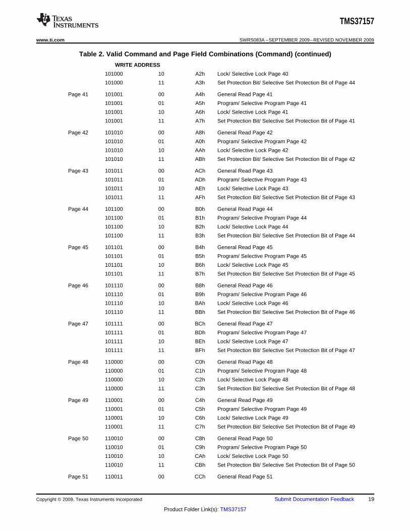
Table 2. Valid Command and Page Field Combinations (Command) (continued)
WRITE ADDRESS
101000 10 A2h Lock/ Selective Lock Page 40
101000 11 A3h Set Protection Bit/ Selective Set Protection Bit of Page 44
Page 41 101001 00 A4h General Read Page 41
101001 01 A5h Program/ Selective Program Page 41
101001 10 A6h Lock/ Selective Lock Page 41
101001 11 A7h Set Protection Bit/ Selective Set Protection Bit of Page 41
Page 42 101010 00 A8h General Read Page 42
101010 01 A0h Program/ Selective Program Page 42
101010 10 AAh Lock/ Selective Lock Page 42
101010 11 ABh Set Protection Bit/ Selective Set Protection Bit of Page 42
Page 43 101011 00 ACh General Read Page 43
101011 01 ADh Program/ Selective Program Page 43
101011 10 AEh Lock/ Selective Lock Page 43
101011 11 AFh Set Protection Bit/ Selective Set Protection Bit of Page 43
Page 44 101100 00 B0h General Read Page 44
101100 01 B1h Program/ Selective Program Page 44
101100 10 B2h Lock/ Selective Lock Page 44
101100 11 B3h Set Protection Bit/ Selective Set Protection Bit of Page 44
Page 45 101101 00 B4h General Read Page 45
101101 01 B5h Program/ Selective Program Page 45
101101 10 B6h Lock/ Selective Lock Page 45
101101 11 B7h Set Protection Bit/ Selective Set Protection Bit of Page 45
Page 46 101110 00 B8h General Read Page 46
101110 01 B9h Program/ Selective Program Page 46
101110 10 BAh Lock/ Selective Lock Page 46
101110 11 BBh Set Protection Bit/ Selective Set Protection Bit of Page 46
Page 47 101111 00 BCh General Read Page 47
101111 01 BDh Program/ Selective Program Page 47
101111 10 BEh Lock/ Selective Lock Page 47
101111 11 BFh Set Protection Bit/ Selective Set Protection Bit of Page 47
Page 48 110000 00 C0h General Read Page 48
110000 01 C1h Program/ Selective Program Page 48
110000 10 C2h Lock/ Selective Lock Page 48
110000 11 C3h Set Protection Bit/ Selective Set Protection Bit of Page 48
Page 49 110001 00 C4h General Read Page 49
110001 01 C5h Program/ Selective Program Page 49
110001 10 C6h Lock/ Selective Lock Page 49
110001 11 C7h Set Protection Bit/ Selective Set Protection Bit of Page 49
Page 50 110010 00 C8h General Read Page 50
110010 01 C9h Program/ Selective Program Page 50
110010 10 CAh Lock/ Selective Lock Page 50
110010 11 CBh Set Protection Bit/ Selective Set Protection Bit of Page 50
Page 51 110011 00 CCh General Read Page 51
Copyright © 2009, Texas Instruments Incorporated Submit Documentation Feedback 19
Product Folder Link(s): TMS37157
129.3 µs 118.8 µs
0 1 10
123.7 kHz 123.7 kHz134.7 kHz134.7 kHz
TMS37157
SWRS083A –SEPTEMBER 2009–REVISED NOVEMBER 2009 www.ti.com
Table 2. Valid Command and Page Field Combinations (Command) (continued)
WRITE ADDRESS
110011 01 CDh Program/ Selective Program Page 51
110011 10 CEh Lock/ Selective Lock Page 51
110011 11 CFh Set Protection Bit/ Selective Set Protection Bit of Page 51
Page 52 110100 00 D0h General Read Page 52
110100 01 D1h Program/ Selective Program Page 52
110100 10 D2h Lock/ Selective Lock Page 52
110100 11 D3h Set Protection Bit/ Selective Set Protection Bit of Page 52
Page 53 110101 00 D4h General Read Page 53
110101 01 D5h Program/ Selective Program Page 53
110101 10 D6h Lock/ Selective Lock Page 53
110101 11 D7h Set Protection Bit/ Selective Set Protection Bit of Page 53
Page 54 110110 00 D8h Lock/ Selective Lock Page 54
110110 01 D9h Program/Selective Page 54
110110 10 DAh Lock/Selective Lock Page 54
110110 11 DBh Set Protection Bit/ Selective Set Protection Bit of Page 54
Page 55 110111 00 DCh General Read Page 55
110111 01 DDh Program/Selective Page 55
110111 10 DEh Lock/Selective Lock Page 55
110111 11 DFh Set Protection Bit/ Selective Set Protection Bit of Page 55
Read Formats
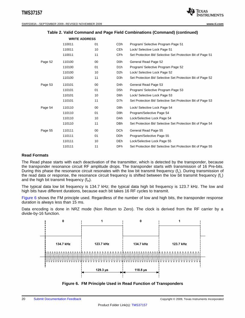
The Read phase starts with each deactivation of the transmitter, which is detected by the transponder, becausethe transponder resonance circuit RF amplitude drops. The transponder starts with transmission of 16 Pre-bits.During this phase the resonance circuit resonates with the low bit transmit frequency (fL). During transmission ofthe read data or response, the resonance circuit frequency is shifted between the low bit transmit frequency (fL)and the high bit transmit frequency (fH).
The typical data low bit frequency is 134.7 kHz; the typical data high bit frequency is 123.7 kHz. The low andhigh bits have different durations, because each bit takes 16 RF cycles to transmit.
Figure 6 shows the FM principle used. Regardless of the number of low and high bits, the transponder responseduration is always less than 15 ms.
Data encoding is done in NRZ mode (Non Return to Zero). The clock is derived from the RF carrier by adivide-by-16 function.
Figure 6. FM Principle Used in Read Function of Transponders
20 Submit Documentation Feedback Copyright © 2009, Texas Instruments Incorporated
Product Folder Link(s): TMS37157
TMS37157
www.ti.com SWRS083A –SEPTEMBER 2009–REVISED NOVEMBER 2009
After a charge phase only, having no write phase, the transponder discharges its capacitor at the end of thepre-bit phase, which results in no response. If a valid function was detected during the write phase, the completeread data format is transmitted. The content of the read data format depends on the previously executedfunction.
When the last bit has been sent, the capacitor is discharged. During discharge no charge-up is possible.
A sufficiently long read time (tRD) must be provided to ensure that the complete read data format can bereceived.
During the response (read) phase, the transponder transmits 96 bits of data, formatted as described below. Thecontent of the response depends on which page was addressed.
All read data starts with a 16-bit preamble followed by an 8-bit start byte (7Eh), and ends with the 8-bit ReadAddress and 16-bit Read Frame BCC. All parts of the read data are transmitted LSB first.
The Read Address byte comprises a 2-bit Status field, which is transmitted first and contains status information,and a 6-bit Page field, which contains page and additional status information. The contents of the Status fielddepend on which page is being addressed.
Table 3. Overview of Read Data Format Content
READ DATA FORMAT BYTE
Page 4 5 6 7 8 9
1 Sel. Address Page 2 Man. Code Serial No. Serial No. Serial No.
2 Sel. Address Page 2 Man. Code Serial No. Serial No. Serial No.
3 Sel. Address Page 2 Man. Code Serial No. Serial No. Serial No.
8 Page 2 Page 8 Page 8 Page 8 Page 8 Page 8
9 Page 2 Page 9 Page 9 Page 9 Page 9 Page 9
10 Page 2 Page 10 Page 10 Page 10 Page 10 Page 10
11 Page 2 Page 11 Page 11 Page 11 Page 11 Page 11
12 Page 2 Page 12 Page 12 Page 12 Page 12 Page 12
13 Page 2 Page 13 Page 13 Page 13 Page 13 Page 13
14 Page 2 Page 14 Page 14 Page 14 Page 14 Page 14
15 Page 2 Page 15 Page 14 Page 14 Page 14 Page 14
19 Battery level ‘00000000’ ‘00000000’ ‘00000000’ ‘00000000’ ‘00000000’
31 MSP Data MSP Data MSP Data MSP Data MSP Data MSP Data
40 Page 2 Page 40 Page 40 Page 40 Page 40 Page 40
41 Page 2 Page 41 Page 41 Page 41 Page 41 Page 41
42 Page 2 Page 42 Page 42 Page 42 Page 42 Page 42
43 Page 2 Page 43 Page 43 Page 43 Page 43 Page 43
44 Page 2 Page 44 Page 44 Page 44 Page 44 Page 44
45 Page 2 Page 45 Page 45 Page 45 Page 45 Page 45
46 Page 2 Page 46 Page 46 Page 46 Page 46 Page 46
47 Page 2 Page 47 Page 47 Page 47 Page 47 Page 47
48 Page 2 Page 48 Page 48 Page 48 Page 48 Page 48
49 Page 2 Page 49 Page 49 Page 49 Page 49 Page 49
50 Page 2 Page 50 Page 50 Page 50 Page 50 Page 50
51 Page 2 Page 51 Page 51 Page 51 Page 51 Page 51
52 Page 2 Page 52 Page 52 Page 52 Page 52 Page 52
53 Page 2 Page 53 Page 53 Page 53 Page 53 Page 53
54 Page 2 Page 54 Page 54 Page 54 Page 54 Page 54
55 Page 2 Page 55 Page 55 Page 55 Page 55 Page 55
Copyright © 2009, Texas Instruments Incorporated Submit Documentation Feedback 21
Product Folder Link(s): TMS37157
TMS37157
SWRS083A –SEPTEMBER 2009–REVISED NOVEMBER 2009 www.ti.com
Table 4 to Table 5 show the valid Status and Page field combinations supported by the TMS37157.
Table 4. Valid Responses, If Page 1 to 3 is Addressed
READER TRANSPONDER
Write Function Write Address Read Address Valid Responses
General Read Page 1 to 3 000001 00 000001 00 Read unlocked Page 1…3………. ………. 10 Read locked Page 1…3000011 000011
Selective Read Page 1 to 3 000001 11 000001 00 Read unlocked Page 1…3………. ………. 10 Read locked Page 1…3000011 000011
Program/Selective Program 000001 01 000001 01 Programming done on Page 1…3Page 1 to 3 ………. ………. 10 Read locked Page 1…3 programming not executed
000011 00001100 Read unlocked Page 1…3, programming not
executed (field strength too low)
000000 01 Programming Page 1…3 done, but possibly notreliable
Lock / Selective Lock 000001 10 000001 10 Read locked Page 1…3Page 1 to 3 ………. ………. 00 Read unlocked Page 1…3, locking not execute
000011 000011 (field strength too low)
000000 00 Read unlocked Page 1…3, locking not correctlyexecuted
10 Read locked Page 1…3, but locking possibly notreliable
Table 5. Valid Responses, if Page 8 to 15 is Addressed
READER TRANSPONDER
Write Function Write Address Read Address Possible Responses
General Read Page 8…15 001000 00 001000 00 Read unlocked Page 8…15……… ……… 10 Read locked Page 8…15001111 001111
Program/ Sel. Program 001000 01 001000 01 Page 8…15 is locked, programming not executedPage 8...15 ……… ……… 10 Page 40…55 is locked, programming not executed
001111 00111100 Page 8…15 is unlocked, programming not
executed (field strength too low)
0000000 01 Programming Page 8…15 done, but possibly notreliable
Lock/ Selective Lock 001000 10 001000 10 Read locked Page 8…15Page 8…15 ……… ……… 00 Read unlocked Page 8…15, locking not executed
001111 001111 (field strength too low)
0000000 00 Read unlocked Page 8…15, locking not correctlyexecuted
10 Read locked Page 8…15, but locking possibly notreliable
Set/ Selective Set Protection 001000 11 001000 00 Read unlocked Page 8…15, Protection bit was notBit ……… ……… set (field strength too low)Page 8…15 001111 001111 10 Read locked Page 8…15, Protection bit was not
set (field strength too low)
11 Protection Bit of Page 8...15 was set
0000000 11 Setting of Protection bit was executed, but possiblynot reliable
22 Submit Documentation Feedback Copyright © 2009, Texas Instruments Incorporated
Product Folder Link(s): TMS37157
TMS37157
www.ti.com SWRS083A –SEPTEMBER 2009–REVISED NOVEMBER 2009
Table 6. Valid Responses, If Battery Check (Page 19) is Addressed
READER TRANSPONDER
Write Function Write Address Read Address Valid Responses
Read Page 19 010011 00 010011 00 Read unlocked Page 19(Battery Check)
Table 7. Valid Responses if MSP Access (Page 31) is Addressed
READER TRANSPONDER
Write Function Write Address Read Address Possible Responses
011111 01 011111 01 MSP Access execution O.K.
00 SPI Programming failedProgram Page 31(MSP Access) 000000 00 MSP Access execution failed
01 MSP Access execution failed
Table 8. Valid Responses, if Page 40 to 55 is Addressed
READER TRANSPONDER
Write Function Write Address Read Address Possible Responses
General Read Page 101000 00 101000 00 Read / unlocked Page 40…5540…55 ……… ……… 10 Read / locked Page 40…55
110110 110110
Program/ Sel. Program 101000 01 101000 01 Programming done on Page 40…55Page 40...55 ……… ……… 10 Page 40…55 is locked, programming not executed
110110 11011000 Page 40…55 is unlocked, programming not
executed (field strength too low)
0 01 Programming Page 40…55 done, but possibly notreliable
Lock/ Selective Lock 101000 10 101000 10 Read locked Page 40…55Page 40…55 ……… ……… 00 Read unlocked Page 40…55, locking not executed
110110 110110 (field strength too low)
0000000 00 Read unlocked Page 40…55, locking not correctlyexecuted
10 Read locked Page 40…55, but locking possibly notreliable
Set/ Selective Set 101000 11 101000 00 Read unlocked Page 40…55, Protection bit wasProtection Bit ……… ……… not set (field strength too low)Page 40…55 110110 110110 10 Read locked Page 40…55, Protection bit was not
set (field strength too low)
11 Protection Bit of Page 40...55 was set
000000 11 Setting of Protection bit was executed, but possiblynot reliable
Copyright © 2009, Texas Instruments Incorporated Submit Documentation Feedback 23
Product Folder Link(s): TMS37157
CHARGEWrite
AdressRead or
discharge
CHARGEWrite
AdressFrame BCC
Read ordischarge
SelectiveAdress
CHARGE WriteAdress
Write data Frame BCC Read ordischarge
ttxCHARGE
tprog
CHARGE WriteAdress
Frame BCCSelectiveAdress
Write datattx Read ordischarge
CHARGEtprog
WriteAdress
Frame BCC Read ordischarge
CHARGEtprog
CHARGEttx
WriteAdress
SelectiveAdress
Frame BCC Read ordischarge
CHARGEtprog
CHARGEttx
TMS37157
SWRS083A –SEPTEMBER 2009–REVISED NOVEMBER 2009 www.ti.com
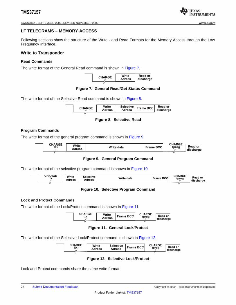
LF TELEGRAMS – MEMORY ACCESS
Following sections show the structure of the Write - and Read Formats for the Memory Access through the LowFrequency Interface.
Write to Transponder
Read Commands
The write format of the General Read command is shown in Figure 7.
Figure 7. General Read/Get Status Command
The write format of the Selective Read command is shown in Figure 8.
Figure 8. Selective Read
Program Commands
The write format of the general program command is shown in Figure 9.
Figure 9. General Program Command
The write format of the selective program command is shown in Figure 10.
Figure 10. Selective Program Command
Lock and Protect Commands
The write format of the Lock/Protect command is shown in Figure 11.
Figure 11. General Lock/Protect
The write format of the Selective Lock/Protect command is shown in Figure 12.
Figure 12. Selective Lock/Protect
Lock and Protect commands share the same write format.
24 Submit Documentation Feedback Copyright © 2009, Texas Instruments Incorporated
Product Folder Link(s): TMS37157
PREBITS START DISCHARGE
16 Bits 8 Bits 24 Bits
96 BitsLSB MSB
IDT Man Serial NumberREAD
ADDR.
READ
FRAME BCC
8 Bits 16 Bits8 Bits 8 Bits 8 Bits
Selective
PREBITS START DISCHARGE
16 Bits 8 Bits 40 Bits
96 BitsLSB MSB
User DataRead
ADDR.
Read
FRAME BCC
8 Bits 16 Bits8 Bits
Selective
TMS37157
www.ti.com SWRS083A –SEPTEMBER 2009–REVISED NOVEMBER 2009
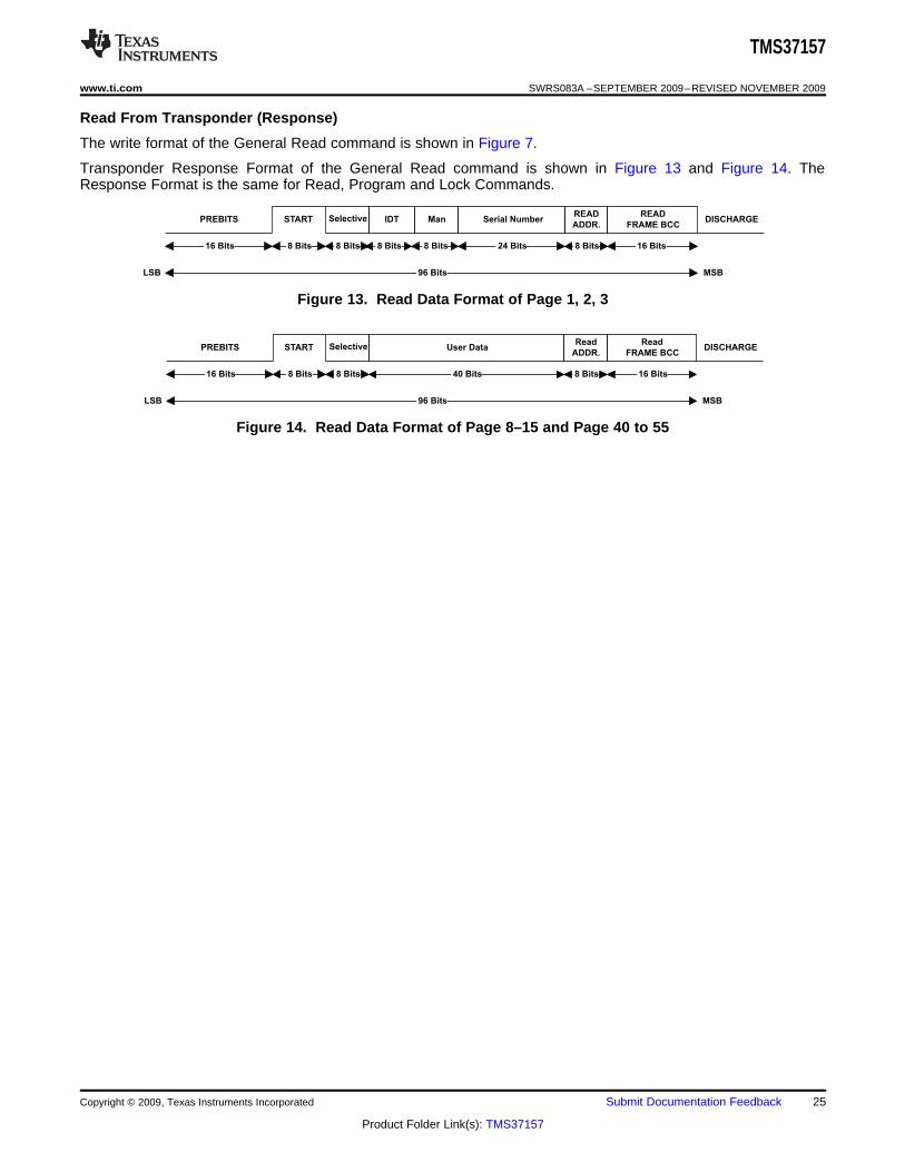
Read From Transponder (Response)
The write format of the General Read command is shown in Figure 7.
Transponder Response Format of the General Read command is shown in Figure 13 and Figure 14. TheResponse Format is the same for Read, Program and Lock Commands.
Figure 13. Read Data Format of Page 1, 2, 3
Figure 14. Read Data Format of Page 8–15 and Page 40 to 55
Copyright © 2009, Texas Instruments Incorporated Submit Documentation Feedback 25
Product Folder Link(s): TMS37157
READ OR
DISCHARGE
8 Bits 16 Bits
WRITE
ADDRESSDATA 0 DATA 5
WRITE
FRAME BCCCHARGECHARGE
10 111110
Page 31Write MSP Data
48 Bits
LSB MSB LSB MSB
PREBITS STARTREAD
ADDRESS
READ
FRAME BCCDISCHARGE
16 Bits 48 Bits8 Bits 8 Bits 16 Bits
96 Bits
MSP DATA
LSB MSB
TMS37157
SWRS083A –SEPTEMBER 2009–REVISED NOVEMBER 2009 www.ti.com
LF TELEGRAMS – SPECIAL FUNCTION
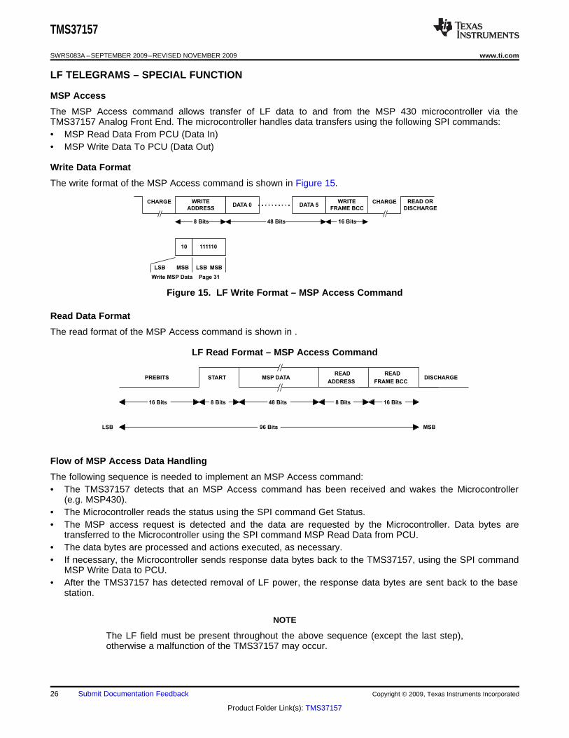
MSP Access
The MSP Access command allows transfer of LF data to and from the MSP 430 microcontroller via theTMS37157 Analog Front End. The microcontroller handles data transfers using the following SPI commands:• MSP Read Data From PCU (Data In)• MSP Write Data To PCU (Data Out)
Write Data Format
The write format of the MSP Access command is shown in Figure 15.
Figure 15. LF Write Format – MSP Access Command
Read Data Format
The read format of the MSP Access command is shown in .
LF Read Format – MSP Access Command
Flow of MSP Access Data Handling
The following sequence is needed to implement an MSP Access command:• The TMS37157 detects that an MSP Access command has been received and wakes the Microcontroller
(e.g. MSP430).• The Microcontroller reads the status using the SPI command Get Status.• The MSP access request is detected and the data are requested by the Microcontroller. Data bytes are
transferred to the Microcontroller using the SPI command MSP Read Data from PCU.• The data bytes are processed and actions executed, as necessary.• If necessary, the Microcontroller sends response data bytes back to the TMS37157, using the SPI command
MSP Write Data to PCU.• After the TMS37157 has detected removal of LF power, the response data bytes are sent back to the base
station.
NOTE
The LF field must be present throughout the above sequence (except the last step),otherwise a malfunction of the TMS37157 may occur.
26 Submit Documentation Feedback Copyright © 2009, Texas Instruments Incorporated
Product Folder Link(s): TMS37157
WRITE
ADDRESS
CHARGE READ OR
DISCHARGE
00 110010
Page 19
LSB MSB
PREBITS STARTBATTERY
LEVELZERO BITS
READ
ADDR.READ FRAME BCC DISCHARGE
16 Bits 40 Bits8 Bits 8 Bits 8 Bits 16 Bits
96 Bits
0 0 0 0 0 0 V V
VV=00:
VV=01:
VV=11:
VBAT < 2.1 V
2.1 V < VBAT < 2.9 V
VBAT > 2.9 V
FULL
EMPTY
2.9 V
2.1 V
TMS37157
www.ti.com SWRS083A –SEPTEMBER 2009–REVISED NOVEMBER 2009
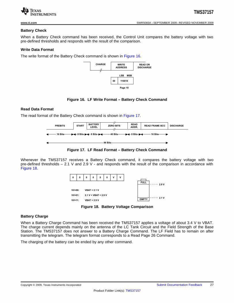
Battery Check
When a Battery Check command has been received, the Control Unit compares the battery voltage with twopre-defined thresholds and responds with the result of the comparison.
Write Data Format
The write format of the Battery Check command is shown in Figure 16.
Figure 16. LF Write Format – Battery Check Command
Read Data Format
The read format of the Battery Check command is shown in Figure 17.
Figure 17. LF Read Format – Battery Check Command
Whenever the TMS37157 receives a Battery Check command, it compares the battery voltage with twopre-defined thresholds – 2.1 V and 2.9 V - and responds with the result of the comparison in accordance withFigure 18.
Figure 18. Battery Voltage Comparison
Battery Charge
When a Battery Charge Command has been received the TMS37157 applies a voltage of about 3.4 V to VBAT.The charge current depends mainly on the antenna of the LC Tank Circuit and the Field Strength of the BaseStation. The TMS37157 does not answer to a Battery Charge Command. The LF Field has to remain on aftertransmitting the telegram. The telegram format corresponds to a Read Page 26 Command.
The charging of the battery can be ended by any other command.
Copyright © 2009, Texas Instruments Incorporated Submit Documentation Feedback 27
Product Folder Link(s): TMS37157
WRITE
ADDRESS
CHARGECharge…..
00 010110
Page 26
LSB MSB
CLK
LENSIMO CMD DATA
SOMI DATADATA
BUSY OK
TMS37157
SWRS083A –SEPTEMBER 2009–REVISED NOVEMBER 2009 www.ti.com
Write Data Format
The write data format of the Battery Charge Command is shown in Figure 19.
Figure 19. Battery Charge Write Command
SPI COMMANDS
The serial interface for communication between a Microcontroller and the TMS37157 is a synchronous SPIinterface which uses clock and data lines to transfer data in bytes. The Microcontroller can use its on-chiphardware USART to implement this interface protocol, which allows efficient Microcontroller operation andsimplifies software development. The USART should be used in synchronous SPI (Serial Peripheral Interface)mode, with the Microcontroller designated as the master for all bi-directional communications.
The TMS37157 uses a 3 wire SPI Communication Interface (SIMO, SOMI, CLK). No Enable is necessary. ForSynchronization the BUSY Output of the TMS37157 can be used.
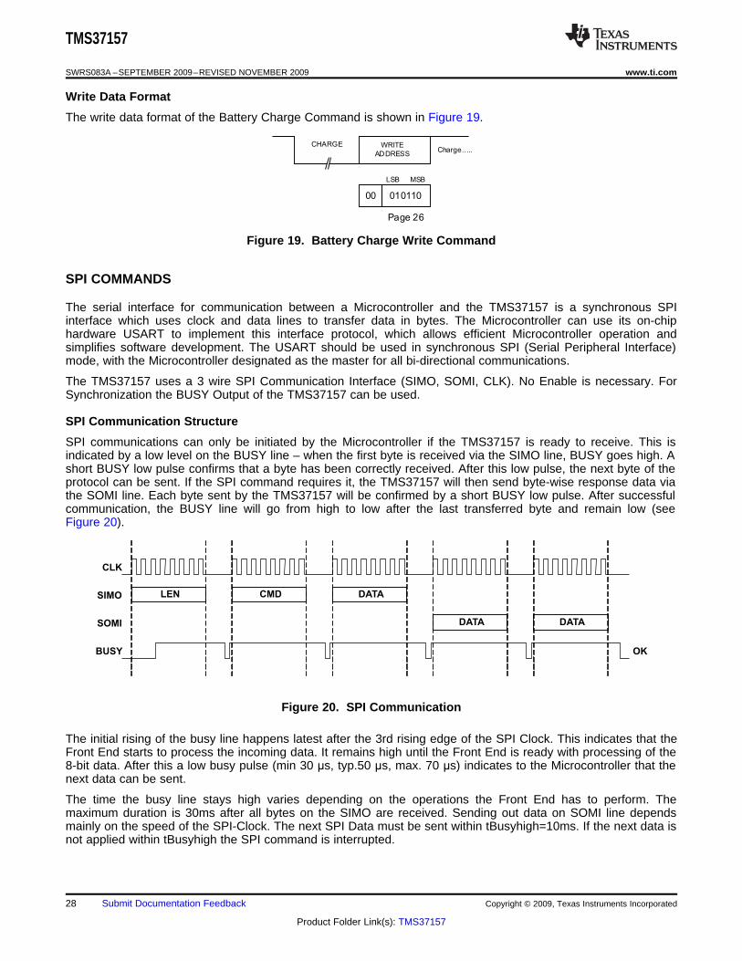
SPI Communication Structure
SPI communications can only be initiated by the Microcontroller if the TMS37157 is ready to receive. This isindicated by a low level on the BUSY line – when the first byte is received via the SIMO line, BUSY goes high. Ashort BUSY low pulse confirms that a byte has been correctly received. After this low pulse, the next byte of theprotocol can be sent. If the SPI command requires it, the TMS37157 will then send byte-wise response data viathe SOMI line. Each byte sent by the TMS37157 will be confirmed by a short BUSY low pulse. After successfulcommunication, the BUSY line will go from high to low after the last transferred byte and remain low (seeFigure 20).
Figure 20. SPI Communication
The initial rising of the busy line happens latest after the 3rd rising edge of the SPI Clock. This indicates that theFront End starts to process the incoming data. It remains high until the Front End is ready with processing of the8-bit data. After this a low busy pulse (min 30 μs, typ.50 μs, max. 70 μs) indicates to the Microcontroller that thenext data can be sent.
The time the busy line stays high varies depending on the operations the Front End has to perform. Themaximum duration is 30ms after all bytes on the SIMO are received. Sending out data on SOMI line dependsmainly on the speed of the SPI-Clock. The next SPI Data must be sent within tBusyhigh=10ms. If the next data isnot applied within tBusyhigh the SPI command is interrupted.
28 Submit Documentation Feedback Copyright © 2009, Texas Instruments Incorporated
Product Folder Link(s): TMS37157
C C X
MSB LSB
CC=00: Transponder Access Command (TAC)
CC=01: n.a.
CC=10: Enhanced Commands (EC)
CC=11: Reserved Commands (RC)
X : Don’t care
X X X X X
TMS37157
www.ti.com SWRS083A –SEPTEMBER 2009–REVISED NOVEMBER 2009
If an error occurs during SPI communication, the BUSY line remains at the level it was when the error occurred.The following three types of error are possible:
Error 1: The TMS37157 stops communication via its SPI interface and indicates this by taking BUSY low. The microcontrollerhas not finished, but BUSY remains low.
Error 2: The TMS37157 is ready to continue communication via its SPI interface and indicates this by taking BUSY high. Themicrocontroller has finished, however, and expects BUSY to remain low. After max. 50ms = tBusyhigh an internalwatchdog shuts down the whole TMS73157 IC.
Error 3: If the TMS37157 receives an invalid command it performs a power down command. This command results in a shutdown of the whole TMS37157 IC.
SPI Protocol Structure
The first 8 bits sent by the microcontroller contain telegram length information (LEN), which defines the numberof following bytes to be transferred via the SIMO line. It is the number of bytes excluding the LEN-byte.
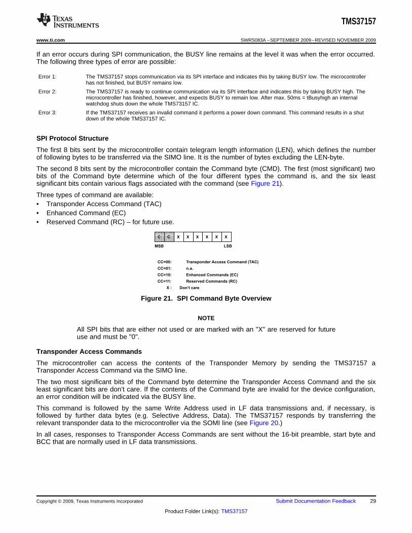
The second 8 bits sent by the microcontroller contain the Command byte (CMD). The first (most significant) twobits of the Command byte determine which of the four different types the command is, and the six leastsignificant bits contain various flags associated with the command (see Figure 21).
Three types of command are available:• Transponder Access Command (TAC)• Enhanced Command (EC)• Reserved Command (RC) – for future use.
Figure 21. SPI Command Byte Overview
NOTE
All SPI bits that are either not used or are marked with an "X" are reserved for futureuse and must be "0".
Transponder Access Commands
The microcontroller can access the contents of the Transponder Memory by sending the TMS37157 aTransponder Access Command via the SIMO line.
The two most significant bits of the Command byte determine the Transponder Access Command and the sixleast significant bits are don’t care. If the contents of the Command byte are invalid for the device configuration,an error condition will be indicated via the BUSY line.
This command is followed by the same Write Address used in LF data transmissions and, if necessary, isfollowed by further data bytes (e.g. Selective Address, Data). The TMS37157 responds by transferring therelevant transponder data to the microcontroller via the SOMI line (see Figure 20.)
In all cases, responses to Transponder Access Commands are sent without the 16-bit preamble, start byte andBCC that are normally used in LF data transmissions.
Copyright © 2009, Texas Instruments Incorporated Submit Documentation Feedback 29
Product Folder Link(s): TMS37157
LEN CMDSIMO
SOMI
Sel.
Addr.DATA DATA *
DATA DATA
WA
Optional
LEN CMD WASIMO
SOMI SEL. ADDR. IDT MAN. SER. NO. SER. NO. SER. NO. RD ADDR.
MSByteLSByte
LEN CMD WASIMO
SOMISEL.
ADDR.IDT MAN. SER. NO. SER. NO. SER. NO. RD ADDR.
MSByteLSByte
SEL.
ADDR.
TMS37157
SWRS083A –SEPTEMBER 2009–REVISED NOVEMBER 2009 www.ti.com
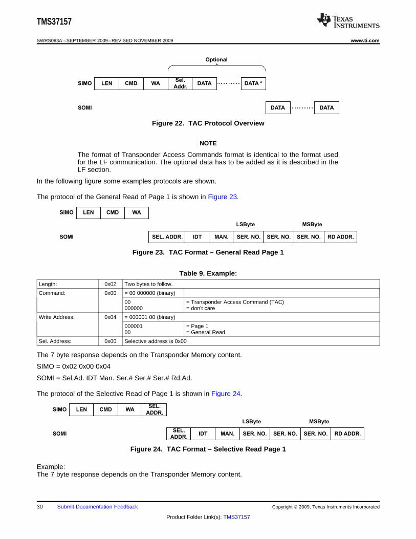
Figure 22. TAC Protocol Overview
NOTE
The format of Transponder Access Commands format is identical to the format usedfor the LF communication. The optional data has to be added as it is described in theLF section.
In the following figure some examples protocols are shown.
The protocol of the General Read of Page 1 is shown in Figure 23.
Figure 23. TAC Format – General Read Page 1
Table 9. Example:
Length: 0x02 Two bytes to follow.
Command: 0x00 = 00 000000 (binary)
00 = Transponder Access Command (TAC)000000 = don’t care
Write Address: 0x04 = 000001 00 (binary)
000001 = Page 100 = General Read
Sel. Address: 0x00 Selective address is 0x00
The 7 byte response depends on the Transponder Memory content.
SIMO = 0x02 0x00 0x04
SOMI = Sel.Ad. IDT Man. Ser.# Ser.# Ser.# Rd.Ad.
The protocol of the Selective Read of Page 1 is shown in Figure 24.
Figure 24. TAC Format – Selective Read Page 1
Example:The 7 byte response depends on the Transponder Memory content.
30 Submit Documentation Feedback Copyright © 2009, Texas Instruments Incorporated
Product Folder Link(s): TMS37157
LEN CMD WASIMO
SOMIBattery
level0x00 RA
WA 010011 00
Read Page
Page 19
=
0x000x000x00 0x00
1 0 MSIMO M M M F F
Command Byte
LSBMSB
M: Mode Bits.
F: Flag Bits.
TMS37157
www.ti.com SWRS083A –SEPTEMBER 2009–REVISED NOVEMBER 2009
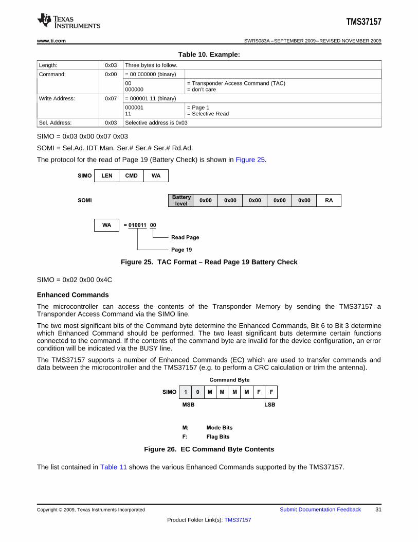
Table 10. Example:
Length: 0x03 Three bytes to follow.
Command: 0x00 = 00 000000 (binary)
00 = Transponder Access Command (TAC)000000 = don’t care
Write Address: 0x07 = 000001 11 (binary)
000001 = Page 111 = Selective Read
Sel. Address: 0x03 Selective address is 0x03
SIMO = 0x03 0x00 0x07 0x03
SOMI = Sel.Ad. IDT Man. Ser.# Ser.# Ser.# Rd.Ad.
The protocol for the read of Page 19 (Battery Check) is shown in Figure 25.
Figure 25. TAC Format – Read Page 19 Battery Check
SIMO = 0x02 0x00 0x4C
Enhanced Commands
The microcontroller can access the contents of the Transponder Memory by sending the TMS37157 aTransponder Access Command via the SIMO line.
The two most significant bits of the Command byte determine the Enhanced Commands, Bit 6 to Bit 3 determinewhich Enhanced Command should be performed. The two least significant buts determine certain functionsconnected to the command. If the contents of the command byte are invalid for the device configuration, an errorcondition will be indicated via the BUSY line.
The TMS37157 supports a number of Enhanced Commands (EC) which are used to transfer commands anddata between the microcontroller and the TMS37157 (e.g. to perform a CRC calculation or trim the antenna).
Figure 26. EC Command Byte Contents
The list contained in Table 11 shows the various Enhanced Commands supported by the TMS37157.
Copyright © 2009, Texas Instruments Incorporated Submit Documentation Feedback 31
Product Folder Link(s): TMS37157
1 0 0SIMO 0 0 0 0 S
Command Byte
LSBMSB
S=0: Start Value is 3791
S=1: Send Start Value
LEN CMD # BYTESIMO
SOMI
DATA DATA
CRC CRC
MSByte
MSByteLSByte
LSByte
TMS37157
SWRS083A –SEPTEMBER 2009–REVISED NOVEMBER 2009 www.ti.com
Table 11. Supported EC Commands
MMMM = 0 = ‘0000’: CRC Calculation Command
MMMM = 1 = ‘0001’: Reserved For Future Use
MMMM = 2 = ‘0010’: Antenna Trimming with Programming Command
MMMM = 3 = ‘0011’: Reserved For Future Use
MMMM = 4 = ‘0100’: Reserved For Future Use
MMMM = 5 = ‘0101’: Oscillator ON Command
MMMM = 6 = ‘0110’: Reserved For Future Use
MMMM = 7 = ‘0111’: CLKA ON command
MMMM = 8 = ‘1000’: Reserved For Future Use
MMMM = 9 = ‘1001’: Reserved For Future Use
MMMM = 10 = ‘1010’: Antenna trimming without Program. Command
MMMM = 11 = ‘1011’: Reserved for Future Use
MMMM = 12 = ‘1100’: MSP Read/Write Data from/to Control Unit
MMMM = 13 = ‘1101’: MSP Read Control Unit Status
MMMM = 14 = ‘1110’: Power Down Command
MMMM = 15 = ‘1111’: Reserved For Future Use
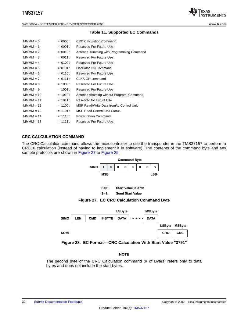
CRC CALCULATION COMMAND
The CRC Calculation command allows the microcontroller to use the transponder in the TMS37157 to perform aCRC16 calculation (instead of having to implement it in software). The contents of the command byte and twosample protocols are shown in Figure 27 to Figure 29.
Figure 27. EC CRC Calculation Command Byte
Figure 28. EC Format – CRC Calculation With Start Value "3791"
NOTE
The second byte of the CRC Calculation command (# of Bytes) refers only to databytes and does not include the start bytes.
32 Submit Documentation Feedback Copyright © 2009, Texas Instruments Incorporated
Product Folder Link(s): TMS37157
LEN CMD # BYTESIMO
SOMI
DATA DATA
CRC CRC
MSByte
MSByteLSByte
LSByte
START START
LSByte MSByte
1 0 1SIMO 0 1 0 0 1
Command Byte
LSBMSB
LEN CMD DATASIMO
SOMI
1 0 0SIMO 0 1 0 0 1
Command Byte
LSBMSB
LEN CMD DATASIMO
SOMI
TMS37157
www.ti.com SWRS083A –SEPTEMBER 2009–REVISED NOVEMBER 2009
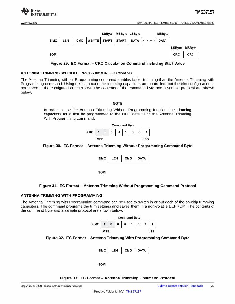
Figure 29. EC Format – CRC Calculation Command Including Start Value
ANTENNA TRIMMING WITHOUT PROGRAMMING COMMAND
The Antenna Trimming without Programming command enables faster trimming than the Antenna Trimming withProgramming command. Using this command the trimming capacitors are controlled, but the trim configuration isnot stored in the configuration EEPROM. The contents of the command byte and a sample protocol are shownbelow.
NOTE
In order to use the Antenna Trimming Without Programming function, the trimmingcapacitors must first be programmed to the OFF state using the Antenna TrimmingWith Programming command.
Figure 30. EC Format – Antenna Trimming Without Programming Command Byte
Figure 31. EC Format – Antenna Trimming Without Programming Command Protocol
ANTENNA TRIMMING WITH PROGRAMMING
The Antenna Trimming with Programming command can be used to switch in or out each of the on-chip trimmingcapacitors. The command programs the trim settings and saves them in a non-volatile EEPROM. The contents ofthe command byte and a sample protocol are shown below.
Figure 32. EC Format – Antenna Trimming With Programming Command Byte
Figure 33. EC Format – Antenna Trimming Command Protocol
Copyright © 2009, Texas Instruments Incorporated Submit Documentation Feedback 33
Product Folder Link(s): TMS37157
1 0 0SIMO 1 0 1 C C
Command Byte
LSBMSB
CC=00: Oscillator Off
CC=01: Oscillator On (134 kHz)
CC=10: Oscillator/4 On (134/4 kHz)
LEN CMDSIMO
SOMI
1 0 0SIMO 1 1 1 X C
Command Byte
LSBMSB
C=0: CLKA Off
C=1: CLKA On
TMS37157
SWRS083A –SEPTEMBER 2009–REVISED NOVEMBER 2009 www.ti.com
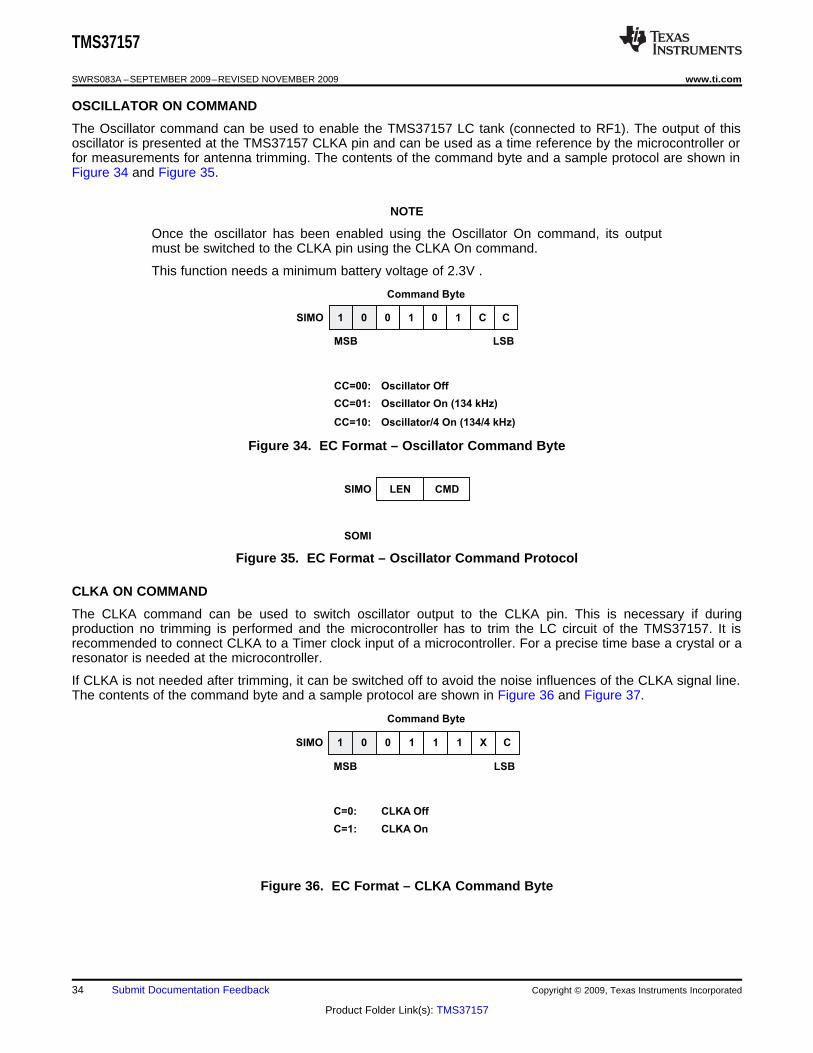
OSCILLATOR ON COMMAND
The Oscillator command can be used to enable the TMS37157 LC tank (connected to RF1). The output of thisoscillator is presented at the TMS37157 CLKA pin and can be used as a time reference by the microcontroller orfor measurements for antenna trimming. The contents of the command byte and a sample protocol are shown inFigure 34 and Figure 35.
NOTE
Once the oscillator has been enabled using the Oscillator On command, its outputmust be switched to the CLKA pin using the CLKA On command.
This function needs a minimum battery voltage of 2.3V .
Figure 34. EC Format – Oscillator Command Byte
Figure 35. EC Format – Oscillator Command Protocol
CLKA ON COMMAND
The CLKA command can be used to switch oscillator output to the CLKA pin. This is necessary if duringproduction no trimming is performed and the microcontroller has to trim the LC circuit of the TMS37157. It isrecommended to connect CLKA to a Timer clock input of a microcontroller. For a precise time base a crystal or aresonator is needed at the microcontroller.
If CLKA is not needed after trimming, it can be switched off to avoid the noise influences of the CLKA signal line.The contents of the command byte and a sample protocol are shown in Figure 36 and Figure 37.
Figure 36. EC Format – CLKA Command Byte
34 Submit Documentation Feedback Copyright © 2009, Texas Instruments Incorporated
Product Folder Link(s): TMS37157
LEN CMDSIMO
SOMI
1 0 1SIMO 1 0 0 0 0
Command Byte
LSBMSB
LEN CMD
DATA 0
SIMO
SOMI DATA 1 DATA 2 DATA 3 DATA 4 DATA 5
1 0 1SIMO 1 0 0 0 1
Command Byte
LSBMSB
LEN CMD DATA 0SIMO
SOMI
DATA 1 DATA 2 DATA 3 DATA 4 DATA 5
STATUS
TMS37157
www.ti.com SWRS083A –SEPTEMBER 2009–REVISED NOVEMBER 2009
Figure 37. EC Format – CLKA Command Protocol
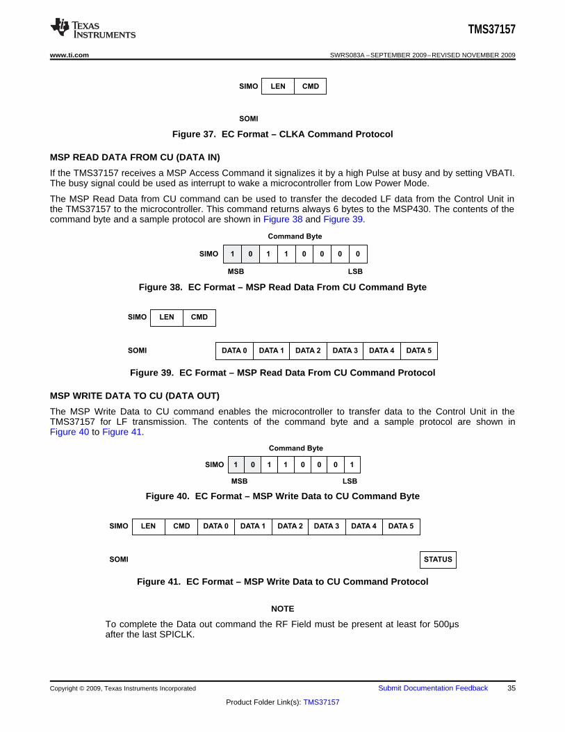
MSP READ DATA FROM CU (DATA IN)
If the TMS37157 receives a MSP Access Command it signalizes it by a high Pulse at busy and by setting VBATI.The busy signal could be used as interrupt to wake a microcontroller from Low Power Mode.
The MSP Read Data from CU command can be used to transfer the decoded LF data from the Control Unit inthe TMS37157 to the microcontroller. This command returns always 6 bytes to the MSP430. The contents of thecommand byte and a sample protocol are shown in Figure 38 and Figure 39.
Figure 38. EC Format – MSP Read Data From CU Command Byte
Figure 39. EC Format – MSP Read Data From CU Command Protocol
MSP WRITE DATA TO CU (DATA OUT)
The MSP Write Data to CU command enables the microcontroller to transfer data to the Control Unit in theTMS37157 for LF transmission. The contents of the command byte and a sample protocol are shown inFigure 40 to Figure 41.
Figure 40. EC Format – MSP Write Data to CU Command Byte
Figure 41. EC Format – MSP Write Data to CU Command Protocol
NOTE
To complete the Data out command the RF Field must be present at least for 500μsafter the last SPICLK.
Copyright © 2009, Texas Instruments Incorporated Submit Documentation Feedback 35
Product Folder Link(s): TMS37157
1 0 1SIMO 1 0 1 0 0
Command Byte
LSBMSB
LEN CMDSIMO
SOMI STATUS MASK
0SIMO 0 0 0 S S
Status Byte
LSBMSB
00
SS=01:
SS=10:
Push
MSP Access
1 0 1SIMO 1 1 0 0 0
Command Byte
LSBMSB
LEN CMDSIMO
SOMI
TMS37157
SWRS083A –SEPTEMBER 2009–REVISED NOVEMBER 2009 www.ti.com
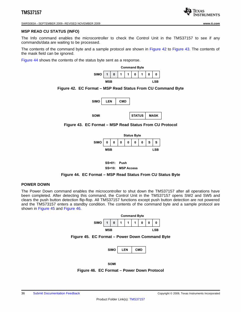
MSP READ CU STATUS (INFO)
The Info command enables the microcontroller to check the Control Unit in the TMS37157 to see if anycommands/data are waiting to be processed.
The contents of the command byte and a sample protocol are shown in Figure 42 to Figure 43. The contents ofthe mask field can be ignored.
Figure 44 shows the contents of the status byte sent as a response.
Figure 42. EC Format – MSP Read Status From CU Command Byte
Figure 43. EC Format – MSP Read Status From CU Protocol
Figure 44. EC Format – MSP Read Status From CU Status Byte
POWER DOWN
The Power Down command enables the microcontroller to shut down the TMS37157 after all operations havebeen completed. After detecting this command, the Control Unit in the TMS37157 opens SW2 and SW5 andclears the push button detection flip-flop. All TMS37157 functions except push button detection are not poweredand the TMS73157 enters a standby condition. The contents of the command byte and a sample protocol areshown in Figure 45 and Figure 46.
Figure 45. EC Format – Power Down Command Byte
Figure 46. EC Format – Power Down Protocol
36 Submit Documentation Feedback Copyright © 2009, Texas Instruments Incorporated
Product Folder Link(s): TMS37157
TCLK
TDAT
TEN
VCL
tTclk = 1/fTclk
tTres tTrc
tTds tTdh
Probe Test Reset Probe Test Write Data
tTdd
Probe Test Read Data
tTclkh tTclkl
TMS37157
www.ti.com SWRS083A –SEPTEMBER 2009–REVISED NOVEMBER 2009
TEST COMMANDS
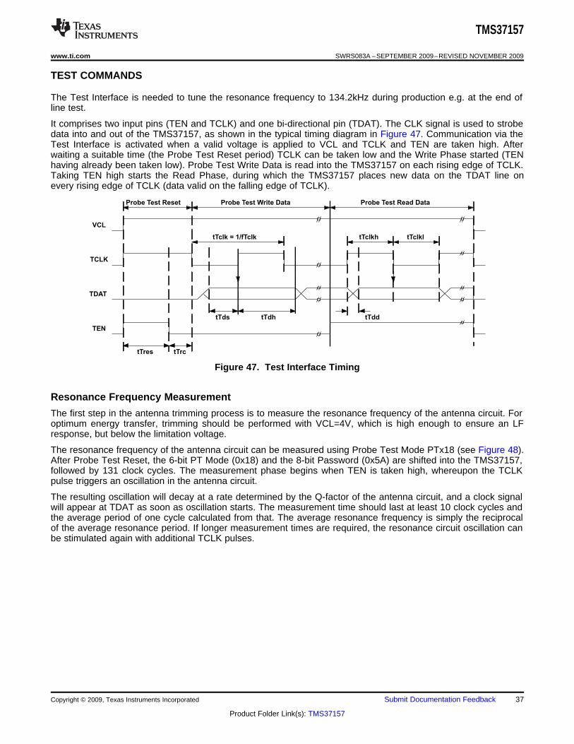
The Test Interface is needed to tune the resonance frequency to 134.2kHz during production e.g. at the end ofline test.
It comprises two input pins (TEN and TCLK) and one bi-directional pin (TDAT). The CLK signal is used to strobedata into and out of the TMS37157, as shown in the typical timing diagram in Figure 47. Communication via theTest Interface is activated when a valid voltage is applied to VCL and TCLK and TEN are taken high. Afterwaiting a suitable time (the Probe Test Reset period) TCLK can be taken low and the Write Phase started (TENhaving already been taken low). Probe Test Write Data is read into the TMS37157 on each rising edge of TCLK.Taking TEN high starts the Read Phase, during which the TMS37157 places new data on the TDAT line onevery rising edge of TCLK (data valid on the falling edge of TCLK).
Figure 47. Test Interface Timing
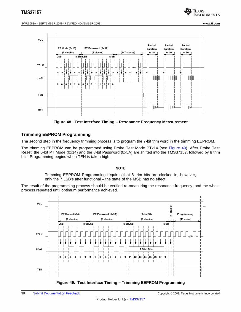
Resonance Frequency Measurement
The first step in the antenna trimming process is to measure the resonance frequency of the antenna circuit. Foroptimum energy transfer, trimming should be performed with VCL=4V, which is high enough to ensure an LFresponse, but below the limitation voltage.
The resonance frequency of the antenna circuit can be measured using Probe Test Mode PTx18 (see Figure 48).After Probe Test Reset, the 6-bit PT Mode (0x18) and the 8-bit Password (0x5A) are shifted into the TMS37157,followed by 131 clock cycles. The measurement phase begins when TEN is taken high, whereupon the TCLKpulse triggers an oscillation in the antenna circuit.
The resulting oscillation will decay at a rate determined by the Q-factor of the antenna circuit, and a clock signalwill appear at TDAT as soon as oscillation starts. The measurement time should last at least 10 clock cycles andthe average period of one cycle calculated from that. The average resonance frequency is simply the reciprocalof the average resonance period. If longer measurement times are required, the resonance circuit oscillation canbe stimulated again with additional TCLK pulses.
Copyright © 2009, Texas Instruments Incorporated Submit Documentation Feedback 37
Product Folder Link(s): TMS37157
0 0 10 01 10 1 0 1 0 1 0
LSB MSBMSBLSB
(8 clocks)(6 clocks)
PT Mode (0x18) PT Password (0x5A)
(147 clocks)
TCLK
TDAT
TEN
VCL
RF1
Period
Duration
>= 10
Period
Duration
>= 10
Period
Duration
>= 10
0 0 1 0 01 10 1 0 1 0 1 0
LSB LSB MSBMSBMSBLSB
(8 clocks)(6 clocks)
PT Mode (0x14) PT Password (0x5A) Trim Bits
(1c
loc
k)
7 Trim Bits
(8 clocks)
Programming
(11 msec)
TCLK
TDAT
TEN
VCL
0T7T1 T2 T3 T4 T5 T6
TMS37157
SWRS083A –SEPTEMBER 2009–REVISED NOVEMBER 2009 www.ti.com
Figure 48. Test Interface Timing – Resonance Frequency Measurement
Trimming EEPROM Programming
The second step in the frequency trimming process is to program the 7-bit trim word in the trimming EEPROM.
The trimming EEPROM can be programmed using Probe Test Mode PTx14 (see Figure 49). After Probe TestReset, the 6-bit PT Mode (0x14) and the 8-bit Password (0x5A) are shifted into the TMS37157, followed by 8 trimbits. Programming begins when TEN is taken high.
NOTE
Trimming EEPROM Programming requires that 8 trim bits are clocked in, however,only the 7 LSB’s after functional – the state of the MSB has no effect.
The result of the programming process should be verified re-measuring the resonance frequency, and the wholeprocess repeated until optimum performance achieved.
Figure 49. Test Interface Timing – Trimming EEPROM Programming
38 Submit Documentation Feedback Copyright © 2009, Texas Instruments Incorporated
Product Folder Link(s): TMS37157
0 0 1 1
LSBMSB
0 1 1 1 1 0 0 1 0 0 0 1
3 7 9 1
TMS37157
www.ti.com SWRS083A –SEPTEMBER 2009–REVISED NOVEMBER 2009
Modulation Frequency Check
During LF transmissions a FSK signal is transmitted. The resonance frequency of the trimmed antenna circuit(fL) represents a low bit and high bits are represented by a lower frequency (fH), which is achieved by switchingin a Modulation Capacitor in parallel with the antenna resonance circuit. This frequency can be measured in thesame way as the normal resonance frequency, but using Probe Test Mode 0x16 instead of 0x18.
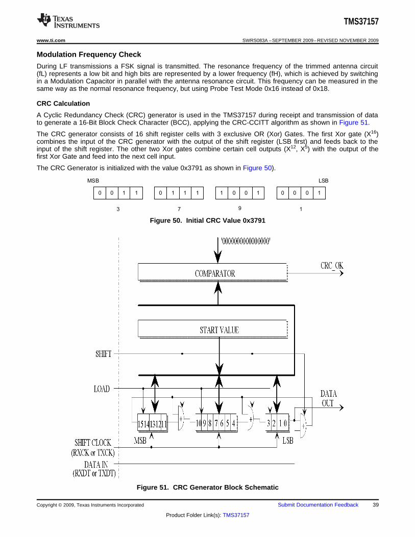
CRC Calculation
A Cyclic Redundancy Check (CRC) generator is used in the TMS37157 during receipt and transmission of datato generate a 16-Bit Block Check Character (BCC), applying the CRC-CCITT algorithm as shown in Figure 51.
The CRC generator consists of 16 shift register cells with 3 exclusive OR (Xor) Gates. The first Xor gate (X16)combines the input of the CRC generator with the output of the shift register (LSB first) and feeds back to theinput of the shift register. The other two Xor gates combine certain cell outputs (X12, X5) with the output of thefirst Xor Gate and feed into the next cell input.
The CRC Generator is initialized with the value 0x3791 as shown in Figure 50).
Figure 50. Initial CRC Value 0x3791
Figure 51. CRC Generator Block Schematic
Copyright © 2009, Texas Instruments Incorporated Submit Documentation Feedback 39
Product Folder Link(s): TMS37157
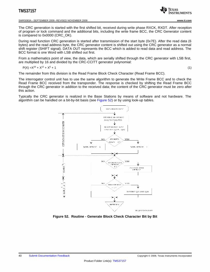
TMS37157
SWRS083A –SEPTEMBER 2009–REVISED NOVEMBER 2009 www.ti.com
The CRC generation is started with the first shifted bit, received during write phase RXCK, RXDT. After receptionof program or lock command and the additional bits, including the write frame BCC, the CRC Generator contentis compared to 0x0000 (CRC_OK).
During read function CRC generation is started after transmission of the start byte (0x7E). After the read data (6bytes) and the read address byte, the CRC generator content is shifted out using the CRC generator as a normalshift register (SHIFT signal). DATA OUT represents the BCC which is added to read data and read address. TheBCC format is one Word with LSB shifted out first.
From a mathematics point of view, the data, which are serially shifted through the CRC generator with LSB first,are multiplied by 16 and divided by the CRC-CCITT generator polynomial:
P(X) =X16 + X12 + X5 + 1 (1)
The remainder from this division is the Read Frame Block Check Character (Read Frame BCC).
The interrogator control unit has to use the same algorithm to generate the Write Frame BCC and to check theRead Frame BCC received from the transponder. The response is checked by shifting the Read Frame BCCthrough the CRC generator in addition to the received data; the content of the CRC generator must be zero afterthis action.
Typically the CRC generator is realized in the Base Stations by means of software and not hardware. Thealgorithm can be handled on a bit-by-bit basis (see Figure 52) or by using look-up tables.
Figure 52. Routine - Generate Block Check Character Bit by Bit
40 Submit Documentation Feedback Copyright © 2009, Texas Instruments Incorporated
Product Folder Link(s): TMS37157
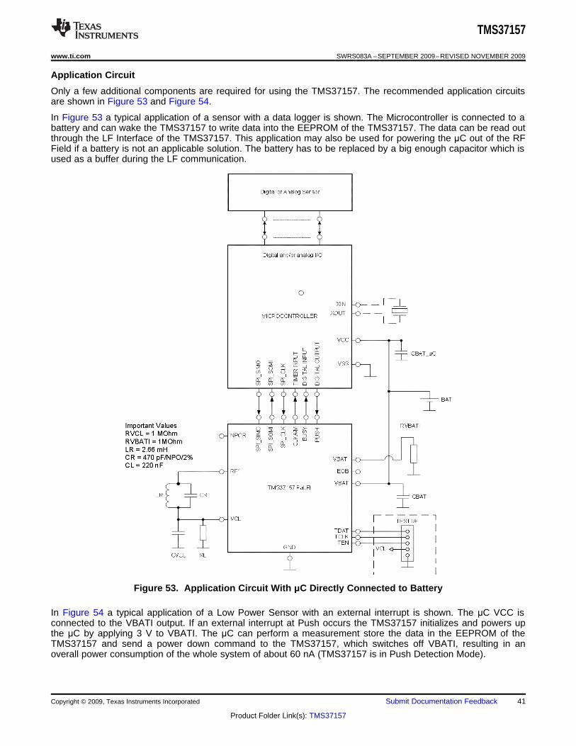
TMS37157
www.ti.com SWRS083A –SEPTEMBER 2009–REVISED NOVEMBER 2009
Application Circuit
Only a few additional components are required for using the TMS37157. The recommended application circuitsare shown in Figure 53 and Figure 54.
In Figure 53 a typical application of a sensor with a data logger is shown. The Microcontroller is connected to abattery and can wake the TMS37157 to write data into the EEPROM of the TMS37157. The data can be read outthrough the LF Interface of the TMS37157. This application may also be used for powering the μC out of the RFField if a battery is not an applicable solution. The battery has to be replaced by a big enough capacitor which isused as a buffer during the LF communication.
Figure 53. Application Circuit With μC Directly Connected to Battery
In Figure 54 a typical application of a Low Power Sensor with an external interrupt is shown. The μC VCC isconnected to the VBATI output. If an external interrupt at Push occurs the TMS37157 initializes and powers upthe μC by applying 3 V to VBATI. The μC can perform a measurement store the data in the EEPROM of theTMS37157 and send a power down command to the TMS37157, which switches off VBATI, resulting in anoverall power consumption of the whole system of about 60 nA (TMS37157 is in Push Detection Mode).
Copyright © 2009, Texas Instruments Incorporated Submit Documentation Feedback 41
Product Folder Link(s): TMS37157
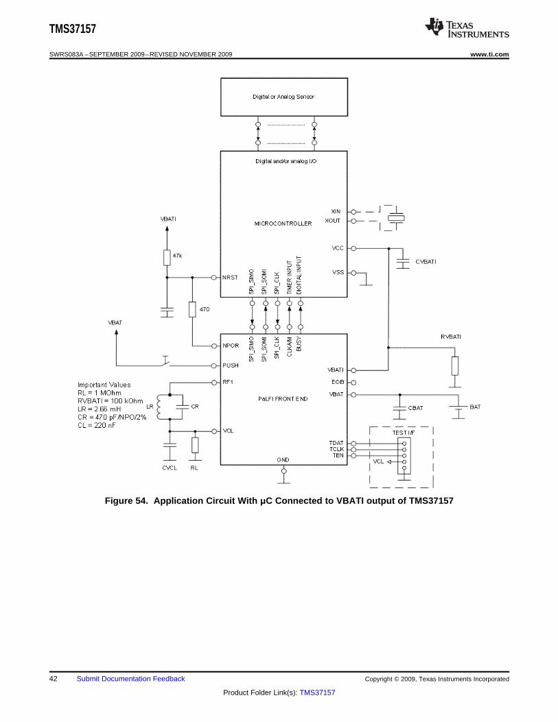
TMS37157
SWRS083A –SEPTEMBER 2009–REVISED NOVEMBER 2009 www.ti.com
Figure 54. Application Circuit With μC Connected to VBATI output of TMS37157
42 Submit Documentation Feedback Copyright © 2009, Texas Instruments Incorporated
Product Folder Link(s): TMS37157
PACKAGE OPTION ADDENDUM
www.ti.com 11-Apr-2013
Addendum-Page 1
PACKAGING INFORMATION
Orderable Device Status(1)
Package Type PackageDrawing
Pins PackageQty
Eco Plan(2)
Lead/Ball Finish MSL Peak Temp(3)
Op Temp (°C) Top-Side Markings(4)
Samples
TMS37157IRSARG4 ACTIVE QFN RSA 16 3000 Green (RoHS& no Sb/Br)
CU NIPDAU Level-2-260C-1 YEAR -40 to 85 37157I
(1) The marketing status values are defined as follows:ACTIVE: Product device recommended for new designs.LIFEBUY: TI has announced that the device will be discontinued, and a lifetime-buy period is in effect.NRND: Not recommended for new designs. Device is in production to support existing customers, but TI does not recommend using this part in a new design.PREVIEW: Device has been announced but is not in production. Samples may or may not be available.OBSOLETE: TI has discontinued the production of the device.
(2) Eco Plan - The planned eco-friendly classification: Pb-Free (RoHS), Pb-Free (RoHS Exempt), or Green (RoHS & no Sb/Br) - please check http://www.ti.com/productcontent for the latest availabilityinformation and additional product content details.TBD: The Pb-Free/Green conversion plan has not been defined.Pb-Free (RoHS): TI's terms "Lead-Free" or "Pb-Free" mean semiconductor products that are compatible with the current RoHS requirements for all 6 substances, including the requirement thatlead not exceed 0.1% by weight in homogeneous materials. Where designed to be soldered at high temperatures, TI Pb-Free products are suitable for use in specified lead-free processes.Pb-Free (RoHS Exempt): This component has a RoHS exemption for either 1) lead-based flip-chip solder bumps used between the die and package, or 2) lead-based die adhesive used betweenthe die and leadframe. The component is otherwise considered Pb-Free (RoHS compatible) as defined above.Green (RoHS & no Sb/Br): TI defines "Green" to mean Pb-Free (RoHS compatible), and free of Bromine (Br) and Antimony (Sb) based flame retardants (Br or Sb do not exceed 0.1% by weightin homogeneous material)
(3) MSL, Peak Temp. -- The Moisture Sensitivity Level rating according to the JEDEC industry standard classifications, and peak solder temperature.
(4) Multiple Top-Side Markings will be inside parentheses. Only one Top-Side Marking contained in parentheses and separated by a "~" will appear on a device. If a line is indented then it is acontinuation of the previous line and the two combined represent the entire Top-Side Marking for that device.
Important Information and Disclaimer:The information provided on this page represents TI's knowledge and belief as of the date that it is provided. TI bases its knowledge and belief on informationprovided by third parties, and makes no representation or warranty as to the accuracy of such information. Efforts are underway to better integrate information from third parties. TI has taken andcontinues to take reasonable steps to provide representative and accurate information but may not have conducted destructive testing or chemical analysis on incoming materials and chemicals.TI and TI suppliers consider certain information to be proprietary, and thus CAS numbers and other limited information may not be available for release.
In no event shall TI's liability arising out of such information exceed the total purchase price of the TI part(s) at issue in this document sold by TI to Customer on an annual basis.
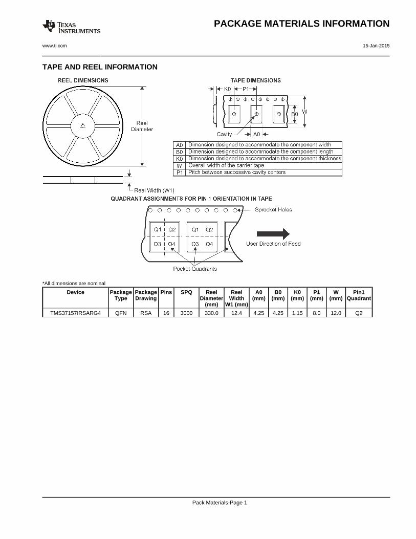
TAPE AND REEL INFORMATION
*All dimensions are nominal
Device PackageType
PackageDrawing
Pins SPQ ReelDiameter
(mm)
ReelWidth
W1 (mm)
A0(mm)
B0(mm)
K0(mm)
P1(mm)
W(mm)
Pin1Quadrant
TMS37157IRSARG4 QFN RSA 16 3000 330.0 12.4 4.25 4.25 1.15 8.0 12.0 Q2
PACKAGE MATERIALS INFORMATION
www.ti.com 15-Jan-2015
Pack Materials-Page 1
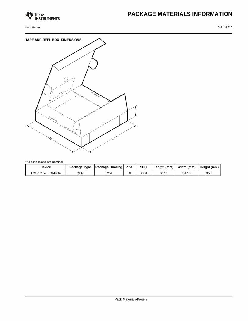
*All dimensions are nominal
Device Package Type Package Drawing Pins SPQ Length (mm) Width (mm) Height (mm)
TMS37157IRSARG4 QFN RSA 16 3000 367.0 367.0 35.0
PACKAGE MATERIALS INFORMATION
www.ti.com 15-Jan-2015
Pack Materials-Page 2
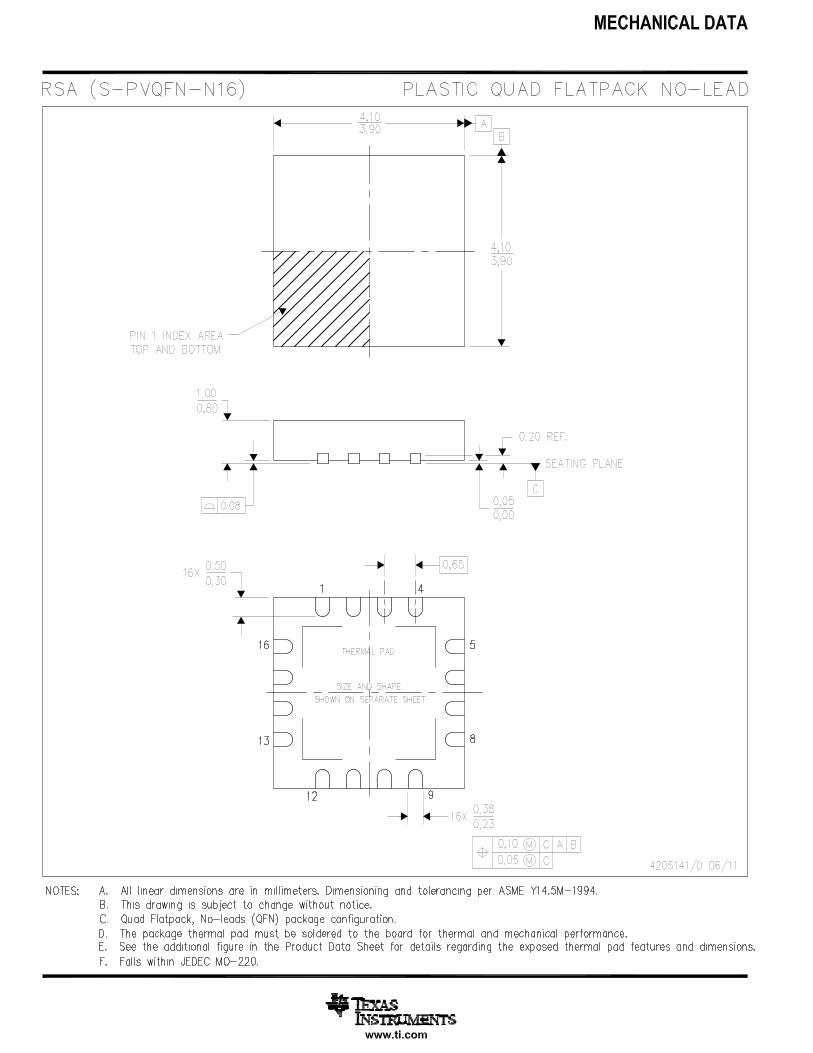

IMPORTANT NOTICE
Texas Instruments Incorporated and its subsidiaries (TI) reserve the right to make corrections, enhancements, improvements and otherchanges to its semiconductor products and services per JESD46, latest issue, and to discontinue any product or service per JESD48, latestissue. Buyers should obtain the latest relevant information before placing orders and should verify that such information is current andcomplete. All semiconductor products (also referred to herein as “components”) are sold subject to TI’s terms and conditions of salesupplied at the time of order acknowledgment.TI warrants performance of its components to the specifications applicable at the time of sale, in accordance with the warranty in TI’s termsand conditions of sale of semiconductor products. Testing and other quality control techniques are used to the extent TI deems necessaryto support this warranty. Except where mandated by applicable law, testing of all parameters of each component is not necessarilyperformed.TI assumes no liability for applications assistance or the design of Buyers’ products. Buyers are responsible for their products andapplications using TI components. To minimize the risks associated with Buyers’ products and applications, Buyers should provideadequate design and operating safeguards.TI does not warrant or represent that any license, either express or implied, is granted under any patent right, copyright, mask work right, orother intellectual property right relating to any combination, machine, or process in which TI components or services are used. Informationpublished by TI regarding third-party products or services does not constitute a license to use such products or services or a warranty orendorsement thereof. Use of such information may require a license from a third party under the patents or other intellectual property of thethird party, or a license from TI under the patents or other intellectual property of TI.Reproduction of significant portions of TI information in TI data books or data sheets is permissible only if reproduction is without alterationand is accompanied by all associated warranties, conditions, limitations, and notices. TI is not responsible or liable for such altereddocumentation. Information of third parties may be subject to additional restrictions.Resale of TI components or services with statements different from or beyond the parameters stated by TI for that component or servicevoids all express and any implied warranties for the associated TI component or service and is an unfair and deceptive business practice.TI is not responsible or liable for any such statements.Buyer acknowledges and agrees that it is solely responsible for compliance with all legal, regulatory and safety-related requirementsconcerning its products, and any use of TI components in its applications, notwithstanding any applications-related information or supportthat may be provided by TI. Buyer represents and agrees that it has all the necessary expertise to create and implement safeguards whichanticipate dangerous consequences of failures, monitor failures and their consequences, lessen the likelihood of failures that might causeharm and take appropriate remedial actions. Buyer will fully indemnify TI and its representatives against any damages arising out of the useof any TI components in safety-critical applications.In some cases, TI components may be promoted specifically to facilitate safety-related applications. With such components, TI’s goal is tohelp enable customers to design and create their own end-product solutions that meet applicable functional safety standards andrequirements. Nonetheless, such components are subject to these terms.No TI components are authorized for use in FDA Class III (or similar life-critical medical equipment) unless authorized officers of the partieshave executed a special agreement specifically governing such use.Only those TI components which TI has specifically designated as military grade or “enhanced plastic” are designed and intended for use inmilitary/aerospace applications or environments. Buyer acknowledges and agrees that any military or aerospace use of TI componentswhich have not been so designated is solely at the Buyer's risk, and that Buyer is solely responsible for compliance with all legal andregulatory requirements in connection with such use.TI has specifically designated certain components as meeting ISO/TS16949 requirements, mainly for automotive use. In any case of use ofnon-designated products, TI will not be responsible for any failure to meet ISO/TS16949.
Products ApplicationsAudio www.ti.com/audio Automotive and Transportation www.ti.com/automotiveAmplifiers amplifier.ti.com Communications and Telecom www.ti.com/communicationsData Converters dataconverter.ti.com Computers and Peripherals www.ti.com/computersDLP® Products www.dlp.com Consumer Electronics www.ti.com/consumer-appsDSP dsp.ti.com Energy and Lighting www.ti.com/energyClocks and Timers www.ti.com/clocks Industrial www.ti.com/industrialInterface interface.ti.com Medical www.ti.com/medicalLogic logic.ti.com Security www.ti.com/securityPower Mgmt power.ti.com Space, Avionics and Defense www.ti.com/space-avionics-defenseMicrocontrollers microcontroller.ti.com Video and Imaging www.ti.com/videoRFID www.ti-rfid.comOMAP Applications Processors www.ti.com/omap TI E2E Community e2e.ti.comWireless Connectivity www.ti.com/wirelessconnectivity
Mailing Address: Texas Instruments, Post Office Box 655303, Dallas, Texas 75265Copyright © 2015, Texas Instruments Incorporated