Embed Size (px)
Citation preview

Pb-Free Selective Wave Solder Guidelines for Thermally Challenging PCBs
Ramon Mendez1, Helen Lowe2, Ismael Marin1, Celestica Monterrey1, Mexico
Celestica Toronto2, Canada
ABSTRACT As the use of lead-free alloys has increased in electronic assemblies, much work has been done to develop Design for
Manufacturability (DFM) guidelines for the new materials. However, there are still some challenges remaining with wave
solder, which is a complex process with many interacting factors. One such challenge is achieving good Pin Through Hole
(PTH) barrel fill on thicker PCBs, particularly for power/ground pins connected to multiple plane layers. One important
factor in the selective wave solder process is the size of the selective pallet opening around the PTH pins. It has been
observed that larger pallet openings generally provide better barrel fill than smaller ones, but further research is needed t o
determine the recommended pallet opening for more thermally challenging product designs. The recommended pallet
opening can then be used to determine DFM guidelines for the component keep out from the PTH pins on the solder side
of the board.
This paper presents the outcome of a study done with a thick, thermally challenging test vehicle wave soldered using a wide
range of selective pallet opening sizes. The test vehicle is 3.05mm (0.120”) thick with twenty copper layers, including ten
plane layers, and is populated with several PTH component types. Other design variables include pin to hole clearance, and
quantity of plane layers connected to each pin. The PCBs were assembled with a Pb -free alloy (Sn-Ag-Cu) and also SnPb
as a baseline. In the first part of the investigation, a Des ign of Experiment was performed to optimize the wave solder process
parameters and in the second phase, the optimized process parameters were held constant to focus on varying the pallet
opening size only. The results for the various pallet opening sizes and their interaction with the other design factors will be
discussed.
INTRODUCTION
During the early stages of the product life cycle, Design for Manufacturability (DFM) plays an important role in
improving the manufacturability of the product, yields, and cost margins [1]
. By considering the impact on manufacturing
before the design is finalized, the often-competing objectives from design and manufacturing can be addressed and
optimal decisions made in a cost-effective manner. After the design is ‘locked in’, changes become increasingly
difficult and costly to implement.
DFM guidelines must evolve over time to address changes in assembly technology, as well as changes in product design
requirements. In the case of wave solder, the transition from tin-lead (SnPb) to lead-free (Pb-free) solder has necessitated a
re-evaluation of the associated DFM guidelines. At the same time, product functionality requirements in some sectors are
driving increased layer counts, increased quantity of plane layers, and increas ed PCB thickness.
Wave soldering is a complex process involving many variables and design factors and their interactions [2]
. Previous work
has documented the challenges associated with transitioning from SnPb to Pb -free wave soldering, driven by differences in
material properties of the alloys [3]
. These challenges are exacerbated by increasing PCB thickness and thermal mass. For
board designs that require double-sided surface mount technology (SMT) in addition to numerous pin through hole (PTH)
components, selective wave soldering is often used to attach the PTH components. The selective wave solder process uses a
product-specific pallet to shield the SMT components on the bottom side of the board, with apertures to expose the PTH
components’ pins to the wave solder. The distance from the PTH pins to the pallet aperture wall has been shown to have a
strong effect on the assembly yield of the PTH components: reducing the pallet aperture size reduces the PTH barrel fill and
yield [4]
. The pallet aperture size in turn restricts the location of the SMT components to be shielded. The goal is to establish
DFM guidelines for pallet apertures that will produce acceptable assembly results without unduly restricting the design
layout.
This paper focuses on the effect of selective wave solder pallet aperture size on PTH barrel fill, on a relatively thick test
vehicle with a large quantity of plane layers. The test vehicle was chosen to represent a realistic but challenging product
design for Pb-free selective wave solder. The effect of selective pallet aperture size on a variety of component types was
studied, as well as the interaction between aperture size and other design features.
Test vehicles were assembled with both tin-silver-copper (SAC) solder and SnPb solder, in order to better understand the
impact of switching to Pb-free SAC solder for thick, thermally challenging boards. The results with a selective pallet
As originally published in the IPC APEX EXPO Proceedings.
were also compared to those with a fully open pallet. This was done to illustrate the theoretical ‘bes t case’ condition for
selective pallet opening size, and to gauge whether further work with larger selective pallet openings might provide any
further improvement in assembly yield.
TEST VEHICLE
The test vehicle used was a 280mm x 404 mm (11” x 16”) board, 3.00mm (0.120”) thick, with a total of 20 layers,
representative of higher complexity, thermally challenging product types such as server, industrial and telecommunication
products [5]
. The PTH components selected for the test vehicle were based on common ly used components assembled on
telecom boards (Table 1). An existing test vehicle design was modified for use in this study, and a number of existing
locations were left unpopulated. An assembled board is shown in Figure 1. The board finish was OSP HT and the laminate
was TUC622LE. There were a total of 10 plane layers, 8 planes of 1oz copper and 2 planes of 2oz copper. The board stack
up is shown in Figure 2.
Figure 1. Test vehicle with components
Table1. Components assembled
Figure 2 . Board stack-up
As originally published in the IPC APEX EXPO Proceedings.
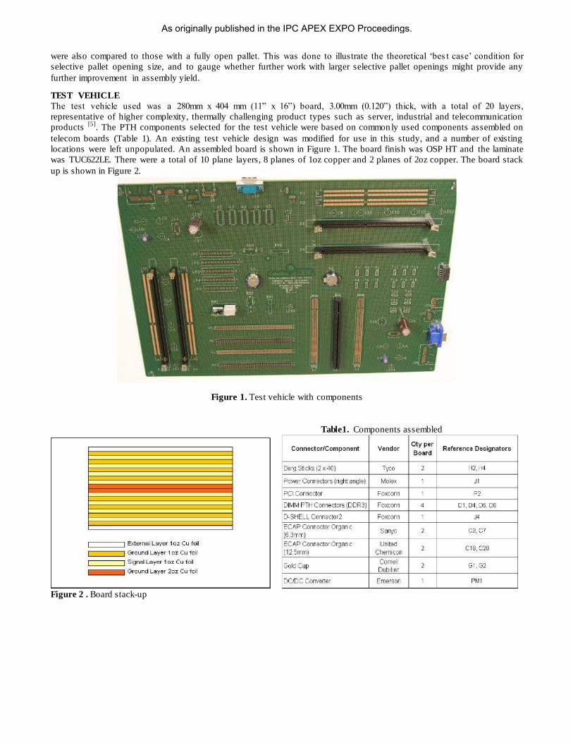
The quantity of ground layers connected to the ground pins varied among the assembled components, and was intended to
simulate representative connections for products. See Figure 3 and Table 2 below for the ground connection details. Figure
3 also shows the travel direction of the board.
Figure 3. Component layout
Table 2. Quantity of ground connections by component
Previous experiments have shown the effect of the pin to hole clearance on the barrel fill, where small clearances provide
lower barrel fill and therefore increase the quantity of defects [1] [6]. The hole sizes used for each component and the
corresponding pin to hole clearances are shown in Table 3.
Table 3. Clearance between pin and barrel wall
As originally published in the IPC APEX EXPO Proceedings.
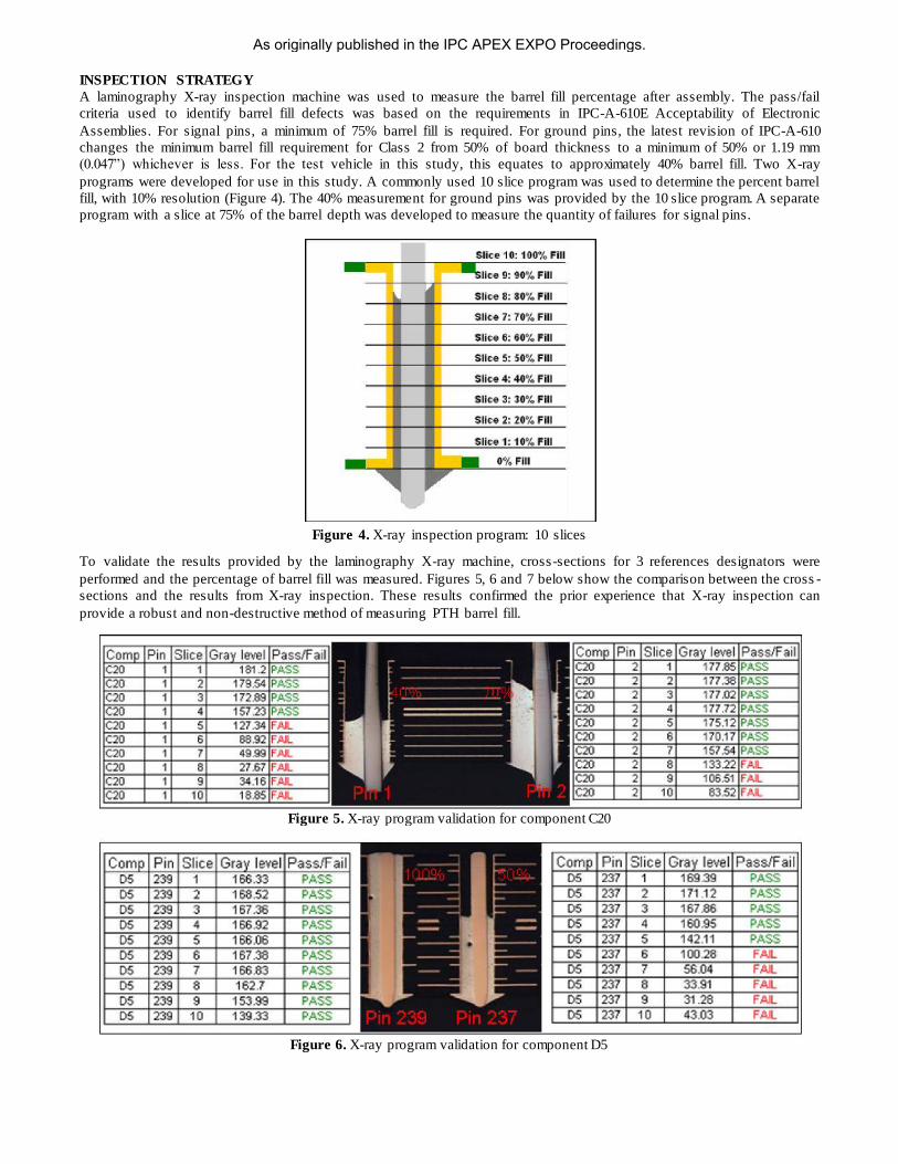
Figure 5. X-ray program validation for component C20
Figure 6. X-ray program validation for component D5
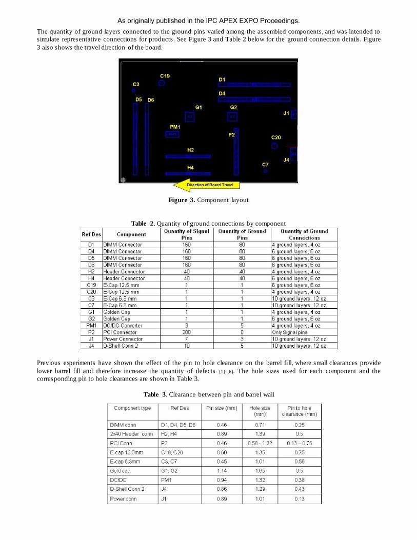
INSPECTION STRATEGY
A laminography X-ray inspection machine was used to measure the barrel fill percentage after assembly. The pass/fail
criteria used to identify barrel fill defects was based on the requirements in IPC-A-610E Acceptability of Electronic
Assemblies. For signal pins, a minimum of 75% barrel fill is required. For ground pins, the latest revision of IPC-A-610
changes the minimum barrel fill requirement for Class 2 from 50% of board thickness to a minimum of 50% or 1.19 mm
(0.047”) whichever is less. For the test vehicle in this study, this equates to approximately 40% barrel fill. Two X-ray
programs were developed for use in this study. A commonly used 10 slice program was used to determine the percent barrel
fill, with 10% resolution (Figure 4). The 40% measurement for ground pins was provided by the 10 slice program. A separate
program with a slice at 75% of the barrel depth was developed to measure the quantity of failures for signal pins.
Figure 4. X-ray inspection program: 10 slices
To validate the results provided by the laminography X-ray machine, cross-sections for 3 references designators were
performed and the percentage of barrel fill was measured. Figures 5, 6 and 7 below show the comparison between the cross -
sections and the results from X-ray inspection. These results confirmed the prior experience that X-ray inspection can
provide a robust and non-destructive method of measuring PTH barrel fill.
As originally published in the IPC APEX EXPO Proceedings.
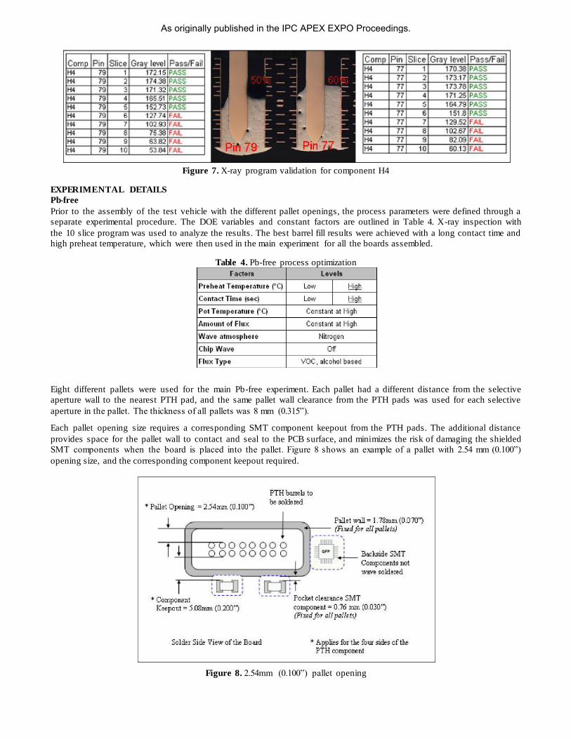
Figure 7. X-ray program validation for component H4
EXPERIMENTAL DETAILS
Pb-free
Prior to the assembly of the test vehicle with the different pallet openings, the process parameters were defined through a
separate experimental procedure. The DOE variables and constant factors are outlined in Table 4. X-ray inspection with
the 10 slice program was used to analyze the results. The best barrel fill results were achieved with a long contact time and
high preheat temperature, which were then used in the main experiment for all the boards assembled.
Table 4. Pb-free process optimization
Eight different pallets were used for the main Pb-free experiment. Each pallet had a different distance from the selective
aperture wall to the nearest PTH pad, and the same pallet wall clearance from the PTH pads was used for each selective
aperture in the pallet. The thickness of all pallets was 8 mm (0.315”).
Each pallet opening size requires a corresponding SMT component keepout from the PTH pads. The additional distance
provides space for the pallet wall to contact and seal to the PCB surface, and minimizes the risk of damaging the shielded
SMT components when the board is placed into the pallet. Figure 8 shows an example of a pallet with 2.54 mm (0.100”)
opening size, and the corresponding component keepout required.
Figure 8. 2.54mm (0.100”) pallet opening
As originally published in the IPC APEX EXPO Proceedings.
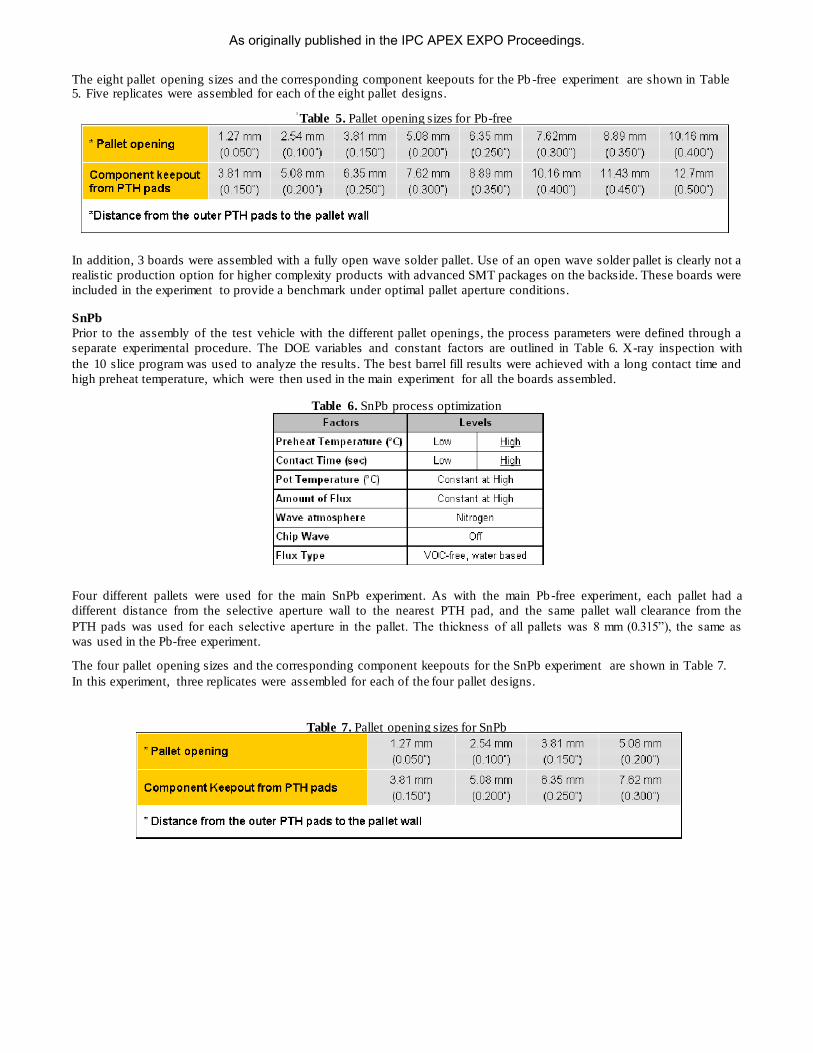
Table 5. Pallet opening sizes for Pb-free
Table 7. Pallet opening sizes for SnPb
The eight pallet opening sizes and the corresponding component keepouts for the Pb -free experiment are shown in Table 5. Five replicates were assembled for each of the eight pallet designs.
In addition, 3 boards were assembled with a fully open wave solder pallet. Use of an open wave solder pallet is clearly not a
realistic production option for higher complexity products with advanced SMT packages on the backside. These boards were
included in the experiment to provide a benchmark under optimal pallet aperture conditions.
SnPb
Prior to the assembly of the test vehicle with the different pallet openings, the process parameters were defined through a
separate experimental procedure. The DOE variables and constant factors are outlined in Table 6. X-ray inspection with
the 10 slice program was used to analyze the results. The best barrel fill results were achieved with a long contact time and
high preheat temperature, which were then used in the main experiment for all the boards assembled.
Table 6. SnPb process optimization
Four different pallets were used for the main SnPb experiment. As with the main Pb-free experiment, each pallet had a
different distance from the selective aperture wall to the nearest PTH pad, and the same pallet wall clearance from the
PTH pads was used for each selective aperture in the pallet. The thickness of all pallets was 8 mm (0.315”), the same as
was used in the Pb-free experiment.
The four pallet opening sizes and the corresponding component keepouts for the SnPb experiment are shown in Table 7.
In this experiment, three replicates were assembled for each of the four pallet designs.
As originally published in the IPC APEX EXPO Proceedings.
RESULTS AND DISCUSSION
Analysis of DIMM connectors: Pb-free solder
The DIMM connectors were analyzed with a General linear model of two factors, the pallet opening size and the component
reference designator. Each reference designator was considered separately as each has a different set of attributes, including
quantity of ground planes connected to the ground pins, orientation relative to the wave solder, and location on the board
relative to the leading end of the board. Barrel fill defects were used for the analysis of the results, with barrel fill lower than
40% considered a defect for ground pins and lower than 75% considered a defect for signal pins. The ANOVA results of the
model are shown in Figure 9. A P-value less than 0.05 indicates that the factor has statistical effect at the 95% confidence
level. The statistical results indicate that the pallet opening and the component attributes both have a significant impact o n the
barrel fill defects.
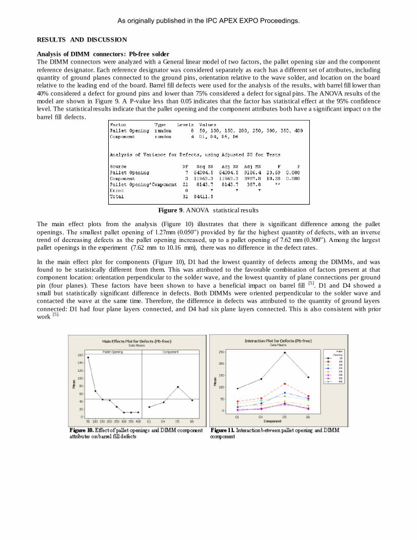
Figure 9. ANOVA statistical results
The main effect plots from the analysis (Figure 10) illustrates that there is significant difference among the pallet
openings. The smallest pallet opening of 1.27mm (0.050”) provided by far the highest quantity of defects, with an inverse
trend of decreasing defects as the pallet opening increased, up to a pallet opening of 7.62 mm (0.300”). Among the largest
pallet openings in the experiment (7.62 mm to 10.16 mm), there was no difference in the defect rates.
In the main effect plot for components (Figure 10), D1 had the lowest quantity of defects among the DIMMs, and was
found to be statistically different from them. This was attributed to the favorable combination of factors present at that
component location: orientation perpendicular to the solder wave, and the lowest quantity of plane connections per ground
pin (four planes). These factors have been shown to have a beneficial impact on barrel fill [5]
. D1 and D4 showed a
small but statistically significant difference in defects. Both DIMMs were oriented perpendicular to the solder wave and
contacted the wave at the same time. Therefore, the difference in defects was attributed to the quantity of ground layers
connected: D1 had four plane layers connected, and D4 had six plane layers connected. This is also consistent with prior
work [5].
As originally published in the IPC APEX EXPO Proceedings.

Figure 12. DIMM layout and direction of board travel
D5 had by far the highest quantity of defects among the DIMMs. It was oriented parallel to the solder wave and was
located
at the leading end of the board such that it was the first DIMM to contact the solder wave. Comparing the results for D5
and
D6 illustrates the beneficial effect of heat transfer from a leading component to a trailing neighbor component. Both
DIMMs were oriented parallel to the wave, and had the same quantity of planes connected to each ground pin (six). The
only difference was the location on the board and therefore the order in which they contacted the wave.
One interesting observation from this study comes from comparing the results for D4 and D6, which were both connected
to the same quantity of planes (six). D4 would appear to have a distinct advantage based on its perpendicular orientation to
the solder wave, relative to D6 which is oriented parallel to the wave. However, the defect rates of these two DIMMs are
not statistically different. D6 benefited greatly from heat transferred to the internal planes by solder flow into the barrels of
D5, the leading DIMM. The beneficial effect on D6 of heat transfer from D5 was sufficient to offset the negative impact
of parallel orientation to the solder wave.
From Figure 11 and Figure 13, it can be seen that increasing the pallet opening diminished the differences between
components. The negative impact on D5 defects due to orientation, plane quantity, and location on the board was not
completely eliminated, but it was greatly reduced with larger pallet openings. The difference in defects between D1 and D4
became negligible with the largest pallet openings. This suggests that the negative impact of a few additional ground plane
connections can to some degree be offset by using larger pallet openings.
Figure 13. DIMM defects at different pallet opening (Pb-free)
Figure 14 shows the interaction between pallet opening, component, and connection type (signal or ground) on percentage of
barrel fill. It can be seen that the ground pins are very sensitive to the pallet opening, with larger openings resulting in
improved barrel fill. For signal pins, the size of the pallet opening does not significantly affect the barrel fill, and high barrel
fill values can be achieved even with very small pallet openings. This is an important consideration if an average barrel fil l
value for the component is considered as an experimental response. The consistently high barrel fill for signal pins could
mask a beneficial effect of the pallet aperture size on ground pin barrel fill, particularly in cases where the proportion of
signal pins to grounds pins is high.
As originally published in the IPC APEX EXPO Proceedings.

As originally published in the IPC APEX EXPO Proceedings.
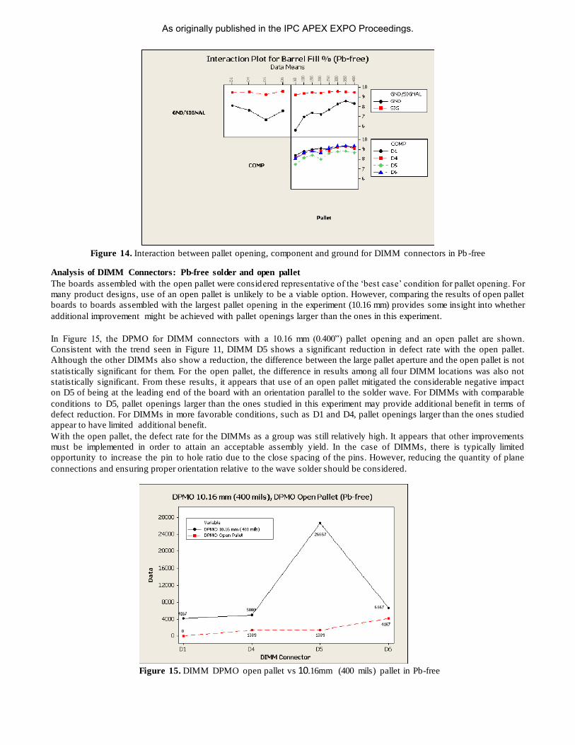
Figure 14. Interaction between pallet opening, component and ground for DIMM connectors in Pb -free
Analysis of DIMM Connectors: Pb-free solder and open pallet
The boards assembled with the open pallet were considered representative of the ‘best case’ condition for pallet opening. For
many product designs, use of an open pallet is unlikely to be a viable option. However, comparing the results of open pallet
boards to boards assembled with the largest pallet opening in the experiment (10.16 mm) provides some insight into whether
additional improvement might be achieved with pallet openings larger than the ones in this experiment.
In Figure 15, the DPMO for DIMM connectors with a 10.16 mm (0.400”) pallet opening and an open pallet are shown.
Consistent with the trend seen in Figure 11, DIMM D5 shows a significant reduction in defect rate with the open pallet.
Although the other DIMMs also show a reduction, the difference between the large pallet aperture and the open pallet is not
statistically significant for them. For the open pallet, the difference in results among all four DIMM locations was also not
statistically significant. From these results, it appears that use of an open pallet mitigated the considerable negative impact
on D5 of being at the leading end of the board with an orientation parallel to the solder wave. For DIMMs with comparable
conditions to D5, pallet openings larger than the ones studied in this experiment may provide additional benefit in terms of
defect reduction. For DIMMs in more favorable conditions, such as D1 and D4, pallet openings larger than the ones studied
appear to have limited additional benefit.
With the open pallet, the defect rate for the DIMMs as a group was still relatively high. It appears that other improvements
must be implemented in order to attain an acceptable assembly yield. In the case of DIMMs, there is typically limited
opportunity to increase the pin to hole ratio due to the close spacing of the pins. However, reducing the quantity of plane
connections and ensuring proper orientation relative to the wave solder should be considered.
Figure 15. DIMM DPMO open pallet vs 10.16mm (400 mils) pallet in Pb-free
As originally published in the IPC APEX EXPO Proceedings.
Panel variable: COMP
Slic
e (Barr
el F
il %)
10 9
8
7
6
5
4
3
2
10 9
8
7
6
5 4
3
2
Scatterplot of Slice (Barrel Fill %) vs Pallet Opening (SnPb)
50 100
D1
D5
150 200
Pallet Opening
50 100
D4
D6
150 200
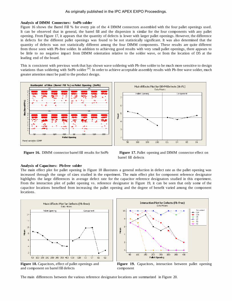
Analysis of DIMM Connectors: SnPb solder
Figure 16 shows the Barrel Fill % for every pin of the 4 DIMM connectors assembled with the four pallet openings used.
It can be observed that in general, the barrel fill and the dispersion is similar for the four components with any pallet
opening. From Figure 17, it appears that the quantity of defects is lower with larger pallet openings. However, the difference
in defects for the different pallet openings was found to be not statistically significant. It was also determined that the
quantity of defects was not statistically different among the four DIMM components. These results are quite different
from those seen with Pb-free solder. In addition to achieving good results with very small pallet openings, there appears to
be little to no negative impact from DIMM orientation relative to the solder wave, or from the location of D5 at the
leading end of the board.
This is consistent with previous work that has shown wave soldering with Pb -free solder to be much more sensitive to design
variations than soldering with SnPb solder [4]
. In order to achieve acceptable assembly results with Pb-free wave solder, much
greater attention must be paid to the product design.
Figure 16. DIMM connector barrel fill results for SnPb Figure 17. Pallet opening and DIMM connector effect on
barrel fill defects
Analysis of Capacitors: Pb-free solder
The main effect plot for pallet opening in Figure 18 illustrates a general reduction in defect rate as the pallet opening was
increased through the range of sizes studied in the experiment. The main effect plot for component reference designator
highlights the large differences in average defect rate for the capacitor reference designators studied in this experiment.
From the interaction plot of pallet opening vs. reference designator in Figure 19, it can be seen that only some of the
capacitor locations benefited from increasing the pallet opening and the degree of benefit varied among the component
locations.
Figure 18. Capacitors, effect of pallet openings and Figure 19. Capacitors, interaction between pallet opening
and component on barrel fill defects component
The main differences between the various reference designator locations are summarized in Figure 20.
As originally published in the IPC APEX EXPO Proceedings.

Figure 20. Capacitors layout and direction of board travel
For the 6.5mm electrolytic capacitors (E-caps) with ten planes connected to the ground pin (C3 and C7), increasing the pallet
opening within the range studied had no impact on the defect rate. The 12.5mm electrolytic capacitors with six or four planes
connected to the ground pin (C19 and C20) showed a gradual improvement as the pallet opening was increased through the
experimental range. For the gold caps with four or six planes connected to the ground pin (G1 and G2), zero defects were
achieved with pallet openings within the range studied. Comparing the results for gold capacitors G1 and G2, there is a
noticeable difference in the smallest pallet aperture size at which optimal results were achieved: 3.81mm (0.150”) for G1
(four planes connected), and 7.62 mm (0.300”) for G2 (six planes connected).
Recent investigations have shown the negative effect on barrel fill of having a high quantity of ground connections and a
small pin to hole clearance [1]
. For PTH E-Caps it been observed that to get successful barrel fill results in Pb-free, larger
clearances between pin and holes are required [6].
The results from the current experiment confirm the importance of the quantity of plane connections for Pb -free wave
solder on thicker PCBs. If permitted by the design requirements, reducing the quantity of planes connected can provide
significant benefits to the Pb-free wave solder yield of PTH E-caps. For a moderate quantity of planes connected (four to six),
increasing the pallet opening size can improve the assembly yield. For a large quantity of plane connections (ten), simply
increasing the pallet opening size may be of limited benefit.
Analysis of Capacitors: Pb-free solder and open pallet
Figure 21 shows the Defects per Board for electrolytic capacitors C19, C20, C3, and C7. The gold capacitors G1 and G2
produced zero defects for the largest experimental pallet opening, so there was no further benefit observed with the open
pallet.
With the open pallet, the defect rate for C19 and C20 was reduced to zero. This suggests that pallet openings larger than the
ones studied in this experiment may provide additional benefit in terms of defect reduction, and supports the trend
indicated in Figure 19. In contrast, C3 and C7 still produced a relatively high average defect rate with the open pallet.
This suggests that although increased pallet openings may provide some improvement for these parts, other
improvements, such as increased pin to hole clearance and reduced quantity of plane connections, must be implemented
in order to achieve an acceptable assembly yield.
Figure 21. Defect per board for C19, C20, C3 and C7 with
10.16 mm pallet opening and open pallet in Pb-free
As originally published in the IPC APEX EXPO Proceedings.
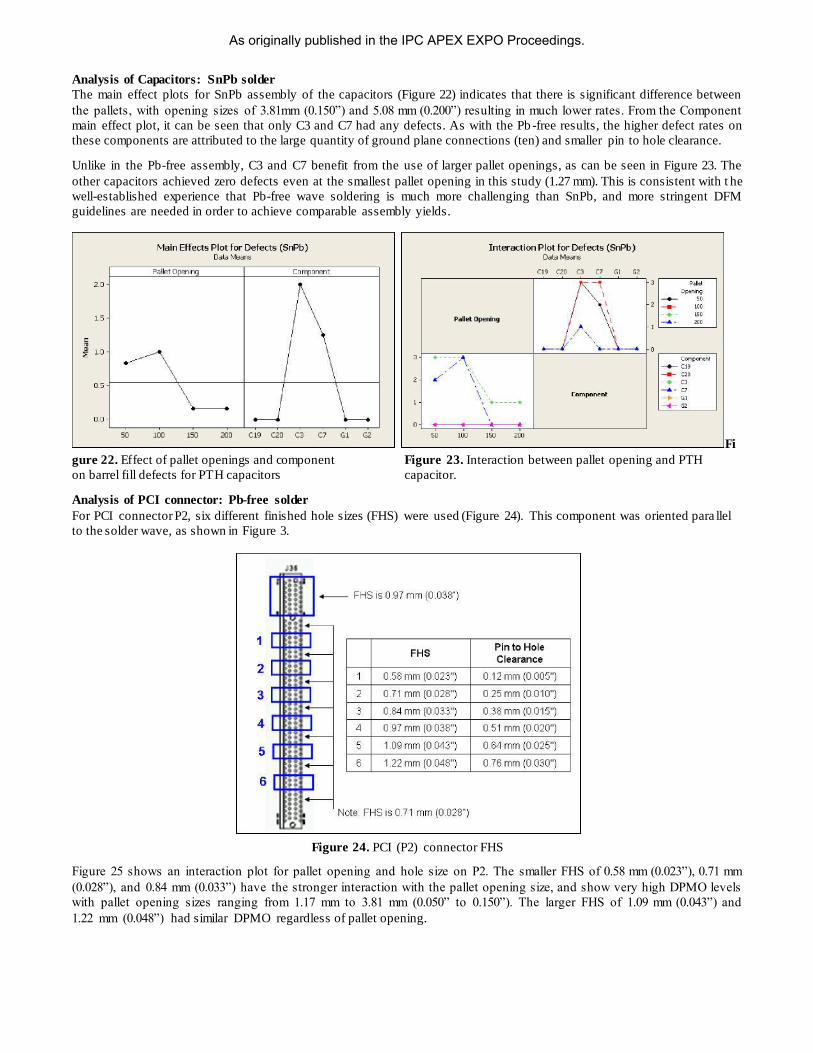
Analysis of Capacitors: SnPb solder
The main effect plots for SnPb assembly of the capacitors (Figure 22) indicates that there is significant difference between
the pallets, with opening sizes of 3.81mm (0.150”) and 5.08 mm (0.200”) resulting in much lower rates. From the Component
main effect plot, it can be seen that only C3 and C7 had any defects. As with the Pb -free results, the higher defect rates on
these components are attributed to the large quantity of ground plane connections (ten) and smaller pin to hole clearance.
Unlike in the Pb-free assembly, C3 and C7 benefit from the use of larger pallet openings, as can be seen in Figure 23. The
other capacitors achieved zero defects even at the smallest pallet opening in this study (1.27 mm). This is consistent with t he
well-established experience that Pb-free wave soldering is much more challenging than SnPb, and more stringent DFM
guidelines are needed in order to achieve comparable assembly yields.
Fi
gure 22. Effect of pallet openings and component Figure 23. Interaction between pallet opening and PTH
on barrel fill defects for PTH capacitors capacitor.
Analysis of PCI connector: Pb-free solder
For PCI connector P2, six different finished hole sizes (FHS) were used (Figure 24). This component was oriented para llel
to the solder wave, as shown in Figure 3.
Figure 24. PCI (P2) connector FHS
Figure 25 shows an interaction plot for pallet opening and hole size on P2. The smaller FHS of 0.58 mm (0.023”), 0.71 mm
(0.028”), and 0.84 mm (0.033”) have the stronger interaction with the pallet opening size, and show very high DPMO levels
with pallet opening sizes ranging from 1.17 mm to 3.81 mm (0.050” to 0.150”). The larger FHS of 1.09 mm (0.043”) and
1.22 mm (0.048”) had similar DPMO regardless of pallet opening.
As originally published in the IPC APEX EXPO Proceedings.
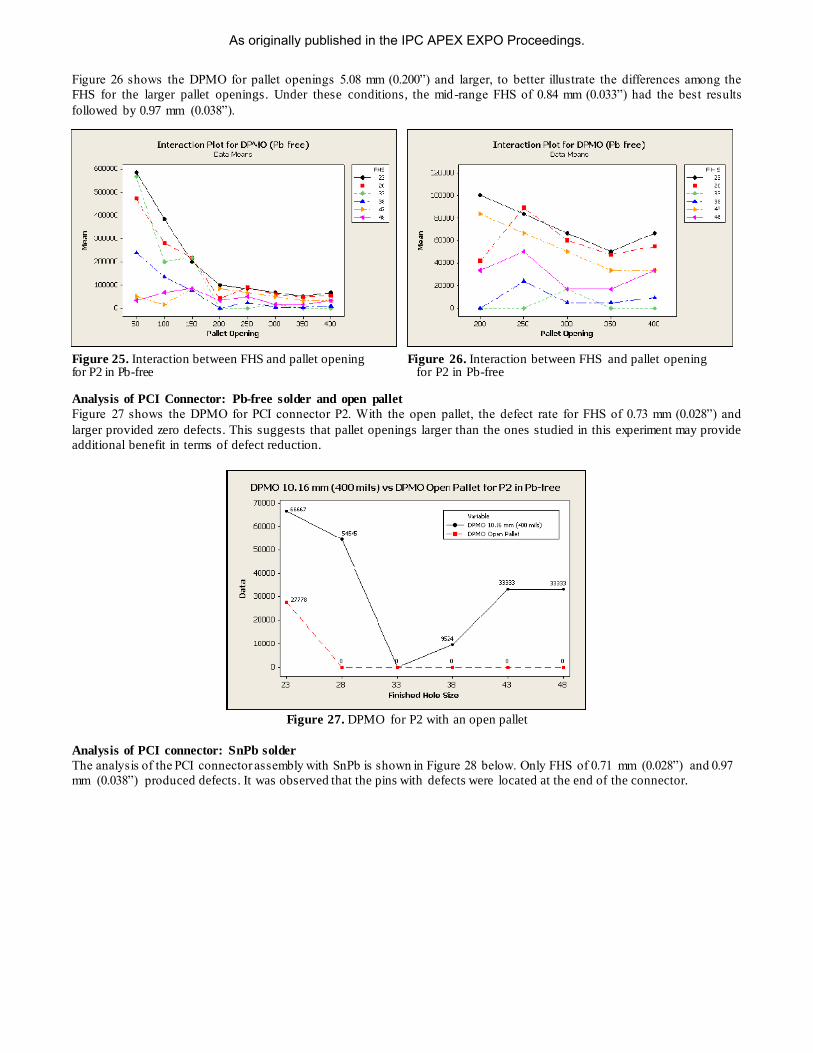
Figure 26 shows the DPMO for pallet openings 5.08 mm (0.200”) and larger, to better illustrate the differences among the
FHS for the larger pallet openings. Under these conditions, the mid-range FHS of 0.84 mm (0.033”) had the best results
followed by 0.97 mm (0.038”).
Figure 25. Interaction between FHS and pallet opening Figure 26. Interaction between FHS and pallet opening for P2 in Pb-free for P2 in Pb-free
Analysis of PCI Connector: Pb-free solder and open pallet
Figure 27 shows the DPMO for PCI connector P2. With the open pallet, the defect rate for FHS of 0.73 mm (0.028”) and
larger provided zero defects. This suggests that pallet openings larger than the ones studied in this experiment may provide
additional benefit in terms of defect reduction.
Figure 27. DPMO for P2 with an open pallet
Analysis of PCI connector: SnPb solder
The analysis of the PCI connector assembly with SnPb is shown in Figure 28 below. Only FHS of 0.71 mm (0.028”) and 0.97
mm (0.038”) produced defects. It was observed that the pins with defects were located at the end of the connector.
As originally published in the IPC APEX EXPO Proceedings.
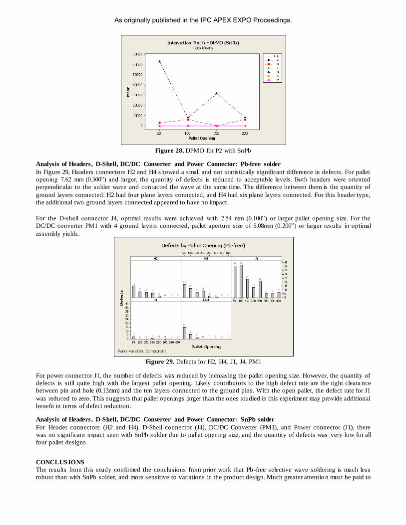
Figure 28. DPMO for P2 with SnPb
Analysis of Headers, D-Shell, DC/DC Converter and Power Connector: Pb-free solder
In Figure 29, Headers connectors H2 and H4 showed a small and not statistically significant difference in defects. For pallet
opening 7.62 mm (0.300”) and larger, the quantity of defects is reduced to acceptable levels. Both headers were oriented
perpendicular to the solder wave and contacted the wave at the same time. The difference between them is the quantity of
ground layers connected: H2 had four plane layers connected, and H4 had six plane layers connected. For this header type,
the additional two ground layers connected appeared to have no impact.
For the D-shell connector J4, optimal results were achieved with 2.54 mm (0.100”) or larger pallet opening size. For the
DC/DC converter PM1 with 4 ground layers connected, pallet aperture size of 5.08mm (0.200”) or larger results in optimal
assembly yields.
Figure 29. Defects for H2, H4, J1, J4, PM1
For power connector J1, the number of defects was reduced by increasing the pallet opening size. However, the quantity of
defects is still quite high with the largest pallet opening. Likely contributors to the high defect rate are the tight cleara nce
between pin and hole (0.13mm) and the ten layers connected to the ground pins. With the open pallet, the defect rate for J1
was reduced to zero. This suggests that pallet openings larger than the ones studied in this experiment may provide additional
benefit in terms of defect reduction.
Analysis of Headers, D-Shell, DC/DC Converter and Power Connector: SnPb solder
For Header connectors (H2 and H4), D-Shell connector (J4), DC/DC Converter (PM1), and Power connector (J1), there
was no significant impact seen with SnPb solder due to pallet opening size, and the quantity of defects was very low for all
four pallet designs. CONCLUS IONS
The results from this study confirmed the conclusions from prior work that Pb -free selective wave soldering is much less
robust than with SnPb solder, and more sensitive to variations in the product design. Much greater attentio n must be paid to
As originally published in the IPC APEX EXPO Proceedings.
design features, such as the component orientation, quantity of plane connections, PTH hole sizes, and SMT keepouts around
the PTH pins, in order to achieve acceptable yields on thick, thermally challenging PCBs.
Key findings related to the selective pallet opening for Pb-free wave solder on a thick, complex board:
In general, increasing the selective pallet opening around the PTH pins is very beneficial with respect to defect
reduction.
The degree of benefit provided by increasing pallet openings is highly dependent on other conditions present, and was
seen to vary based on the component type, pin to hole ratio, component orientation, and the quantity of planes connected.
A selective pallet opening of 7.62 mm (0.300”) can produce acceptable assembly results for most components,
providing DFM guidelines are being followed with respect to other key factors, e.g. the quantity of plane connections,
pin to hole ratio, and use of thermal reliefs. Electrolytic capacitors may require somewhat large r pallet openings to
achieve acceptable results.
If the DFM guidelines for other important factors like plane connections and pin to hole ratio are not followed, simply
increasing the pallet opening may not be sufficient to offset the negative effects and achieve acceptable assembly
results. This is particularly true for more thermally challenging components like electrolytic capacitors. In order for an
increase in pallet opening to be effective in these cases, other changes must also be implemented, for example
reducing the quantity of plane connections.
Some interesting observations in addition to the selective pallet opening results:
Under at least some conditions, heat transfer from a leading component to a trailing neighbor component can be very
beneficial to the trailing neighbor. Additional experiments would be needed to better understand this phenomenon and
how it might be advantageously applied in production board designs.
For the PCI connector, the optimal results with larger pallet openings were attained for holes in the middle of the range
studied. The reasons for this were not immediately evident, and further study is needed to better understand why
larger hole sizes appear to produce more defects than the mid-range ones under this set of conditions.
ACKNOWLEDGEMENTS
The authors wish to thank Javier Aguilar and Jesus Peñaloza for X-Ray machine programming and inspection of the boards,
and Luis Alberto Moya for the cross -sections. Special thanks to Chris Goodall and Danny Imbrogno for their help with the
test vehicle design modifications. Finally, thanks to John McMahon and Craig Hamilton for their consultation and
expertise on this project.
REFERENCES
[1] R Mendez, M Moreno, G Soto, J Herrera, C Hamilton. “Design for Manufacturability in the Lead Free Wave Solder
Process”, APEX, 2008.
[2] J Nguyen, R Thalhamer, D Geiger, D Rooney, and D Shangguan. “Process And Reliability Study Of Lead-Free Wave
Soldering For Large Thick Boards” Corporate Technology Group Flextronics International, SMTA International, 2007.
[3] E. Ferrer, E. Benedetto, G. Freedman, F. Billaut, H. Holder, D. Gonzalez “Reliability of Partially Filled SAC305
Through-Hole Joints”, APEX, Anaheim, CA, S29-02, Feb, 5-10, 2006.
[4] M. Boulos, C. Hamilton, M. Moreno, R. Mendez, G. Soto “Selective Wave Soldering DoE to Develop DFM
Guidelines for Pb & Pb-free Assemblies” Honeywell Aerospace AME; Celestica Inc. SMTA International 2008.
[5] C. Hamilton, J. McMahon, J. Traya, W. Yong Kang, K. Kok Wei; M. Kelly, M. Cole “High Complexity Lead -Free Wave
And Rework: The Effects Of Material, Process And Board Design On Barrel Fill” Celestica Inc.; IBM Corporation,
Conference : SMTA International, 2010.
[6] J. Fangkangwanwong, M. Phuhattsuan, T. Hoon Ng “Lead-Free Wave Soldering For Process And Product Design
Improvement In SnCu Alloys” Celestica Co., Ltd. SMTA International, 2010.
As originally published in the IPC APEX EXPO Proceedings.