Embed Size (px)
Citation preview

DDAATTAA SSHHEEEETT
Product specificationSupersedes data of 2002 Jul 29
2002 Nov 22
INTEGRATED CIRCUITS
PCF8574Remote 8-bit I/O expander forI2C-bus
ARTSCHIPwww.artschip.com

2002 Nov 22 2
ARTSCHIP Semiconductors Product specification
Remote 8-bit I/O expander for I2C-bus PCF8574
CONTENTS
1 FEATURES2 GENERAL DESCRIPTION3 ORDERING INFORMATION4 BLOCK DIAGRAM5 PINNING5.1 DIP16 and SO16 packages5.2 SSOP20 package6 CHARACTERISTICS OF THE I2C-BUS6.1 Bit transfer6.2 Start and stop conditions6.3 System configuration6.4 Acknowledge7 FUNCTIONAL DESCRIPTION7.1 Addressing7.2 Interrupt output7.3 Quasi-bidirectional I/Os8 LIMITING VALUES9 HANDLING10 DC CHARACTERISTICS11 I2C-BUS TIMING CHARACTERISTICS12 PACKAGE OUTLINES13 SOLDERING13.1 Introduction13.2 Through-hole mount packages13.2.1 Soldering by dipping or by solder wave13.2.2 Manual soldering13.3 Surface mount packages13.3.1 Reflow soldering13.3.2 Wave soldering13.3.3 Manual soldering13.4 Suitability of IC packages for wave, reflow and
dipping soldering methods14 DATA SHEET STATUS15 DEFINITIONS16 DISCLAIMERS17 PURCHASE OF ARTSCHIP I2C COMPONENTS

2002 Nov 22 3
Remote 8-bit I/O expander for I2C-bus PCF8574
1 FEATURES
• Operating supply voltage 2.5 to 6 V• Low standby current consumption of 10 µA maximum• I2C-bus to parallel port expander• Open-drain interrupt output• 8-bit remote I/O port for the I2C-bus• Compatible with most microcontrollers• Latched outputs with high current drive capability for
directly driving LEDs• Address by 3 hardware address pins for use of up to
8 devices (up to 16 with PCF8574A)• DIP16, or space-saving SO16 or SSOP20 packages.
2 GENERAL DESCRIPTION
The PCF8574 is a silicon CMOS circuit. It provides generalpurpose remote I/O expansion for most microcontrollerfamilies via the two-line bidirectional bus (I2C-bus).
The device consists of an 8-bit quasi-bidirectional port andan I2C-bus interface. The PCF8574 has a low currentconsumption and includes latched outputs with highcurrent drive capability for directly driving LEDs. It alsopossesses an interrupt line (INT) which can be connectedto the interrupt logic of the microcontroller. By sending aninterrupt signal on this line, the remote I/O can inform themicrocontroller if there is incoming data on its ports withouthaving to communicate via the I2C-bus. This means thatthe PCF8574 can remain a simple slave device.
The PCF8574 and PCF8574A versions differ only in theirslave address as shown in Fig.10.
3 ORDERING INFORMATION
TYPE NUMBERPACKAGE
NAME DESCRIPTION VERSIONPCF8574P;PCF8574AP
DIP16 plastic dual in-line package; 16 leads (300 mil) SOT38-4
PCF8574T;PCF8574AT
SO16 plastic small outline package; 16 leads; body width 7.5 mm SOT162-1
PCF8574TS;PCF8574ATS
SSOP20 plastic shrink small outline package; 20 leads; body width 4.4 mm SOT266-1
ARTSCHIP Semiconductors Product specification

2002 Nov 22 4
ARTSCHIP Semiconductors Product specification
Remote 8-bit I/O expander for I2C-bus PCF8574
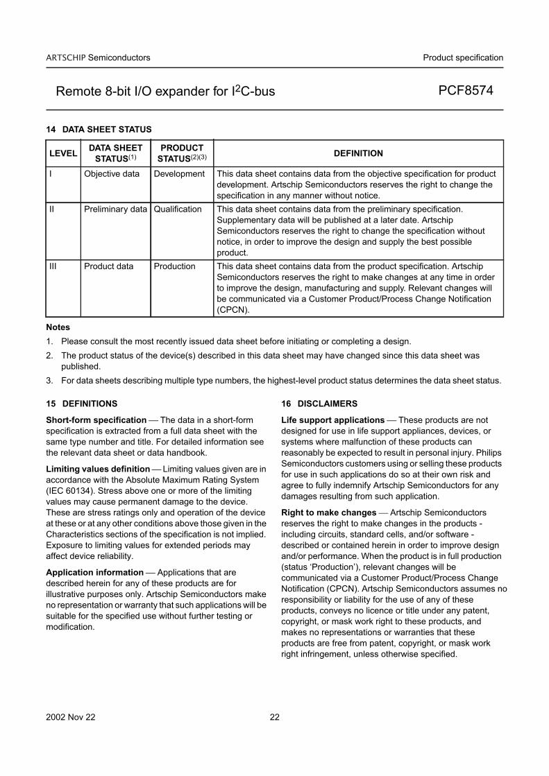
4 BLOCK DIAGRAM
Fig.1 Block diagram (pin numbers apply to DIP16 and SO16 packages).
handbook, full pagewidth
MBD980
I C BUSCONTROL
2INPUTFILTER
1
2
3
14
15
13 INTERRUPTLOGIC
12P7
11P6
10P5
9P4
7P3
6P2
5P1
4P0
8 BIT I/OPORT
SHIFTREGISTER
LP FILTER
WRITE pulse
READ pulsePOWER-ON
RESET
16
8VDDVSS
SDA
SCL
A2
A1
A0
INT
PCF8574
2002 Nov 22 5
ARTSCHIP Semiconductors Product specification
Remote 8-bit I/O expander for I2C-bus PCF8574
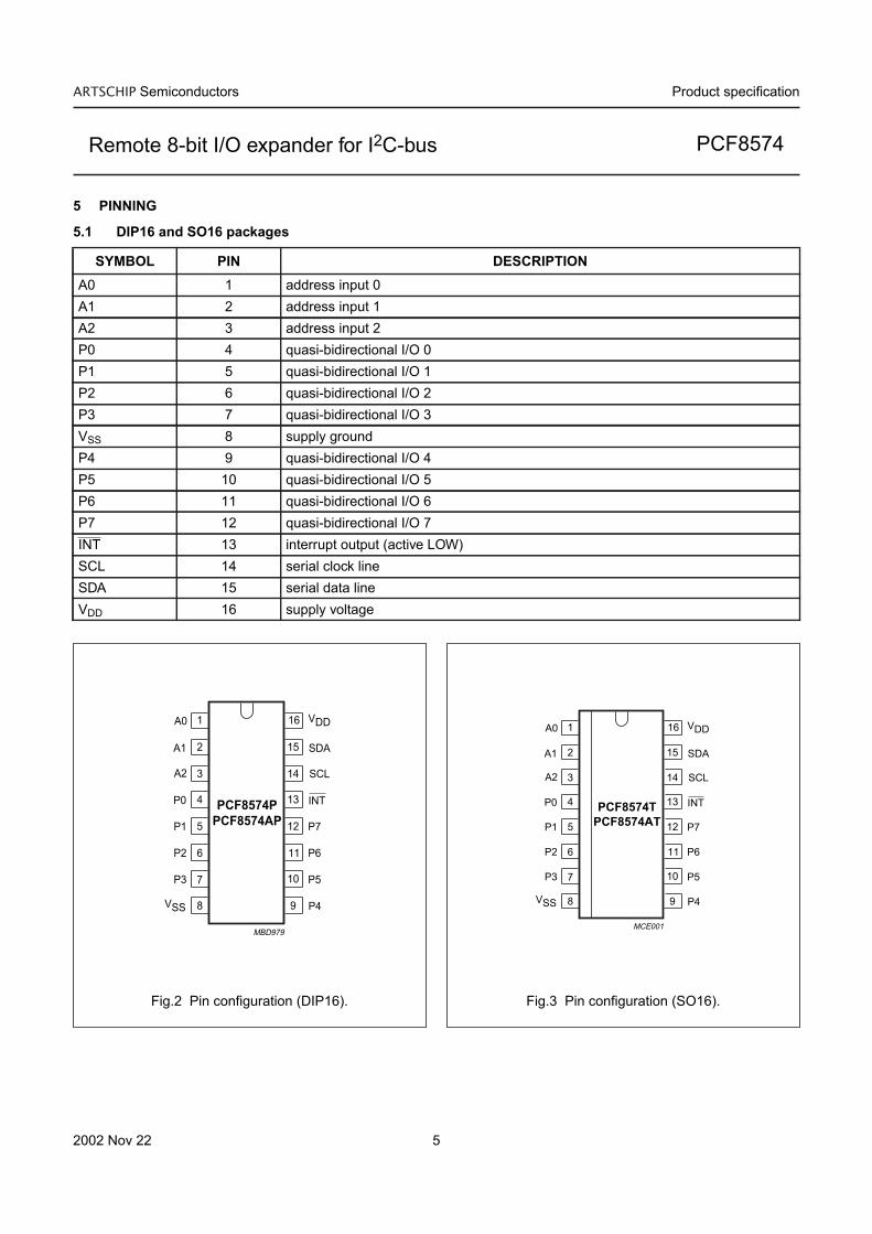
5 PINNING
5.1 DIP16 and SO16 packages
SYMBOL PIN DESCRIPTIONA0 1 address input 0A1 2 address input 1A2 3 address input 2P0 4 quasi-bidirectional I/O 0P1 5 quasi-bidirectional I/O 1P2 6 quasi-bidirectional I/O 2P3 7 quasi-bidirectional I/O 3VSS 8 supply groundP4 9 quasi-bidirectional I/O 4P5 10 quasi-bidirectional I/O 5P6 11 quasi-bidirectional I/O 6P7 12 quasi-bidirectional I/O 7INT 13 interrupt output (active LOW)SCL 14 serial clock lineSDA 15 serial data lineVDD 16 supply voltage
handbook, halfpage1
2
3
4
5
6
7
8
16
15
14
13
12
11
10
9
INT
A0
A1
A2
P0
P1
P2
P3
SDA
VSS
SCL
P7
P6
P5
P4
VDD
PCF8574PPCF8574AP
MBD979
Fig.2 Pin configuration (DIP16).
handbook, halfpage1
2
3
4
5
6
7
8
16
15
14
13
12
11
10
9
INT
A0
A1
A2
P0
P1
P2
P3
SDA
VSS
SCL
P7
P6
P5
P4
VDD
PCF8574TPCF8574AT
MCE001
Fig.3 Pin configuration (SO16).

2002 Nov 22 6
ARTSCHIP Semiconductors Product specification
Remote 8-bit I/O expander for I2C-bus PCF8574
5.2 SSOP20 package
SYMBOL PIN DESCRIPTIONINT 1 interrupt output (active LOW)SCL 2 serial clock linen.c. 3 not connectedSDA 4 serial data lineVDD 5 supply voltageA0 6 address input 0A1 7 address input 1n.c. 8 not connectedA2 9 address input 2P0 10 quasi-bidirectional I/O 0P1 11 quasi-bidirectional I/O 1P2 12 quasi-bidirectional I/O 2n.c. 13 not connectedP3 14 quasi-bidirectional I/O 3VSS 15 supply groundP4 16 quasi-bidirectional I/O 4P5 17 quasi-bidirectional I/O 5n.c. 18 not connectedP6 19 quasi-bidirectional I/O 6P7 20 quasi-bidirectional I/O 7
handbook, halfpage1
2
3
4
5
6
7
8
9
10
20
19
18
17
16
15
14
13
12
11
INT
SCL
n.c.
SDA
VDD
A0
A1
n.c.
A2
P0
P7
P6
n.c.
P5
VSS
P4
P3
n.c.
P2
P1
PCF8574TSPCF8574ATS
MBD978
Fig.4 Pin configuration (SSOP20).

2002 Nov 22 7
ARTSCHIP Semiconductors Product specification
Remote 8-bit I/O expander for I2C-bus PCF8574
6 CHARACTERISTICS OF THE I2C-BUS
The I2C-bus is for 2-way, 2-line communication betweendifferent ICs or modules. The two lines are a serial dataline (SDA) and a serial clock line (SCL). Both lines must beconnected to a positive supply via a pull-up resistor whenconnected to the output stages of a device. Data transfermay be initiated only when the bus is not busy.
6.1 Bit transfer
One data bit is transferred during each clock pulse. Thedata on the SDA line must remain stable during the HIGHperiod of the clock pulse as changes in the data line at thistime will be interpreted as control signals (see Fig.5).
6.2 Start and stop conditions
Both data and clock lines remain HIGH when the bus is notbusy. A HIGH-to-LOW transition of the data line, while theclock is HIGH is defined as the start condition (S).A LOW-to-HIGH transition of the data line while the clockis HIGH is defined as the stop condition (P) (see Fig.6).
6.3 System configuration
A device generating a message is a ‘transmitter’, a devicereceiving is the ‘receiver’. The device that controls themessage is the ‘master’ and the devices which arecontrolled by the master are the ‘slaves’ (see Fig.7).
Fig.5 Bit transfer.
handbook, full pagewidth
MBC621
data linestable;
data valid
changeof dataallowed
SDA
SCL
Fig.6 Definition of start and stop conditions.
handbook, full pagewidth
MBC622
SDA
SCLP
STOP condition
SDA
SCLS
START condition
Fig.7 System configuration.
MBA605
MASTERTRANSMITTER /
RECEIVERSLAVE
RECEIVER
SLAVETRANSMITTER /
RECEIVERMASTER
TRANSMITTER
MASTERTRANSMITTER /
RECEIVER
SDA
SCL

2002 Nov 22 8
ARTSCHIP Semiconductors Product specification
Remote 8-bit I/O expander for I2C-bus PCF8574
6.4 Acknowledge
The number of data bytes transferred between the startand the stop conditions from transmitter to receiver is notlimited. Each byte of eight bits is followed by oneacknowledge bit (see Fig.8). The acknowledge bit is aHIGH level put on the bus by the transmitter whereas themaster generates an extra acknowledge related clockpulse.
A slave receiver which is addressed must generate anacknowledge after the reception of each byte. Also amaster must generate an acknowledge after the reception
of each byte that has been clocked out of the slavetransmitter. The device that acknowledges has to pulldown the SDA line during the acknowledge clock pulse, sothat the SDA line is stable LOW during the HIGH period ofthe acknowledge related clock pulse, set-up and holdtimes must be taken into account.
A master receiver must signal an end of data to thetransmitter by not generating an acknowledge on the lastbyte that has been clocked out of the slave. In this eventthe transmitter must leave the data line HIGH to enable themaster to generate a stop condition.
Fig.8 Acknowledgment on the I2C-bus.
handbook, full pagewidth
MBC602
S
STARTcondition
9821
clock pulse foracknowledgement
not acknowledge
acknowledge
DATA OUTPUTBY TRANSMITTER
DATA OUTPUTBY RECEIVER
SCL FROMMASTER

2002 Nov 22 9
ARTSCHIP Semiconductors Product specification
Remote 8-bit I/O expander for I2C-bus PCF8574
7 FUNCTIONAL DESCRIPTION
Fig.9 Simplified schematic diagram of each I/O.
handbook, full pagewidth
MBD977
D Q
CIS
FF
D Q
CIS
FF
100µA
to interruptlogic
VSS
P0 to P7
VDDwrite pulse
data fromshift register
power-onreset
read pulse
data toshift register
7.1 Addressing
For addressing see Figs 10, 11 and 12.
Fig.10 PCF8574 and PCF8574A slave addresses.
handbook, full pagewidth
MBD973
S 0 1 0 0 A2 A1 A0 0 A 1 0
slave address slave address
AS 0 1 1 A2 A1 A0
a. PCF8574. b. PCF8574A.
Each of the PCF8574’s eight I/Os can be independently used as an input or output. Input data is transferred from theport to the microcontroller by the READ mode (see Fig.12). Output data is transmitted to the port by the WRITE mode(see Fig.11).

redaer taborcA eht ni fdp eht hguorht gnisworb nehw yltcerroc detator eb ot segap epacsdnal ecrof ot etihw ni ereh si txet sihT ni ereh si txet sihT._ nierehsitxetsihTnierehsitxetsihT.redaertaborcAehtnifdpehthguorhtgnisworbnehwyltcerrocdetatorebotsegapepacsdnalecrofotetihw
...ebotsegapepacsdnalecrofotetihw.redaertaborcAehtnifdpehthguorhtgnisworbnehwyltcerrocdetatorebotsegapepacsdnalecrofotetihw
2002N
ov22
10
ARTSCHIP S
emiconductors
Product specification
Rem
ote 8-bit I/O expander for I 2C
-busP
CF8574
andbook, full pagewidth
479DBM
S 0 1 0 0 2A 1A 0A 0 A
noitidnoc trats
1 ATAD
W/R egdelwonkcaevals morf
A 2 ATAD AADS
LCS
OT ETIRWTROP
t vp
TUO ATADTROP MORF
)4758FCP( sserdda evals trop ot atad trop ot atad
87654321
egdelwonkcaevals morf
egdelwonkcaevals morf
t vp
DILAV 2 ATADDILAV 1 ATAD
.)tuptuo( edom ETIRW 11.giF

redaer taborcA eht ni fdp eht hguorht gnisworb nehw yltcerroc detator eb ot segap epacsdnal ecrof ot etihw ni ereh si txet sihT ni ereh si txet sihT._ nierehsitxetsihTnierehsitxetsihT.redaertaborcAehtnifdpehthguorhtgnisworbnehwyltcerrocdetatorebotsegapepacsdnalecrofotetihw
...ebotsegapepacsdnalecrofotetihw.redaertaborcAehtnifdpehthguorhtgnisworbnehwyltcerrocdetatorebotsegapepacsdnalecrofotetihw
2002N
ov22
11
ARTSCHIP S
emiconductors
Product specification
Rem
ote 8-bit I/O expander for I 2C
-busP
CF8574
hand
book
, ful
l pag
ewid
th
579DBM
S 0 1 0 0 2A 1A 0A 1 A
noitidnoc trats
1 ATAD
W/R egdelwonkcaevals morf
A 4 ATAD 1ADS
MORF DAERTROP
t hp
OTNI ATADTROP
)4758FCP( sserdda evals trop morf atad trop morf atad
egdelwonkcaevals morf
potsnoitidnoc
t sp
4 ATAD
P
3 ATAD2 ATAD
t rit rit vi
TNI
.)tupni( edom DAER 21.giF
yna ta deppots eb nac atad fo refsnarT .)P( noitidnoc pots eht sa denifed si HGIH si LCS elihw ,ADS fo noitisnart HGIH-ot-WOL A tneserp atad ,srucco siht nehW .noitidnoc pots a yb tnemom .tsol si atad tupnI .)edom tuptuo( dilav si esahp egdelwonkca tsal eht ta

2002 Nov 22 12
ARTSCHIP Semiconductors Product specification
Remote 8-bit I/O expander for I2C-bus PCF8574
7.2 Interrupt output
The PCF8574 provides an open-drain output (INT) whichcan be fed to a corresponding input of the microcontroller(see Figs 13 and 14). This gives these chips a type ofmaster function which can initiate an action elsewhere inthe system.
An interrupt is generated by any rising or falling edge of theport inputs in the input mode. After time tiv the signal INT isvalid.
Resetting and reactivating the interrupt circuit is achievedwhen data on the port is changed to the original setting ordata is read from or written to the port which has generatedthe interrupt.
Resetting occurs as follows:• In the READ mode at the acknowledge bit after the rising
edge of the SCL signal• In the WRITE mode at the acknowledge bit after the
HIGH-to-LOW transition of the SCL signal
• Interrupts which occur during the acknowledge clockpulse may be lost (or very short) due to the resetting ofthe interrupt during this pulse.
Each change of the I/Os after resetting will be detectedand, after the next rising clock edge, will be transmitted asINT. Reading from or writing to another device does notaffect the interrupt circuit.
7.3 Quasi-bidirectional I/Os
A quasi-bidirectional I/O can be used as an input or outputwithout the use of a control signal for data direction(see Fig.15). At power-on the I/Os are HIGH. In this modeonly a current source to VDD is active. An additional strongpull-up to VDD allows fast rising edges into heavily loadedoutputs. These devices turn on when an output is writtenHIGH, and are switched off by the negative edge of SCL.The I/Os should be HIGH before being used as inputs.
handbook, full pagewidth
MBD976
MICROCONTROLLER
INT INT INT
PCF8574(1)
PCF8574(2)VDD
INT
PCF8574(16)
Fig.13 Application of multiple PCF8574s with interrupt.
Fig.14 Interrupt generated by a change of input to I/O P5.
handbook, full pagewidth
MBD972
S 0 1 0 0 A2 A1 A0 1 A
start condition
1
P5R/W acknowledgefrom slave
1SDA
SCL
DATA INTOP5
t ir
INT
slave address (PCF8574) data from port
1 2 3 4 5 6 7 8
P
stopcondition
t iv

redaer taborcA eht ni fdp eht hguorht gnisworb nehw yltcerroc detator eb ot segap epacsdnal ecrof ot etihw ni ereh si txet sihT ni ereh si txet sihT._ nierehsitxetsihTnierehsitxetsihT.redaertaborcAehtnifdpehthguorhtgnisworbnehwyltcerrocdetatorebotsegapepacsdnalecrofotetihw
...ebotsegapepacsdnalecrofotetihw.redaertaborcAehtnifdpehthguorhtgnisworbnehwyltcerrocdetatorebotsegapepacsdnalecrofotetihw
2002N
ov22
13
ARTSCHIP S
emiconductors
Product specification
Rem
ote 8-bit I/O expander for I 2C
-busP
CF8574
hand
book
, ful
l pag
ewid
th
179DBM
S 0 1 1 1 2A 1A 0A 0 A
noitidnoc trats
1
3PW/R egdelwonkcaevals morf
A 0
3P
A PADS
LCS
3PTUPTUOEGATLOV
I tHO I HO
3PPU-LLUPTUPTUOTNERRUC
)A4758FCP( sserdda evals trop ot atad trop ot atad
87654321
I tnerruc pu-llup tneisnarT 51.giF tHO .WOL ot kcab dna HGIH-ot-WOL morf segnahc 3P elihw

2002 Nov 22 14
ARTSCHIP Semiconductors Product specification
Remote 8-bit I/O expander for I2C-bus PCF8574
8 LIMITING VALUESIn accordance with the Absolute Maximum Rating System (IEC 60134).
9 HANDLING
Inputs and outputs are protected against electrostatic discharge in normal handling. However it is good practice to takenormal precautions appropriate to handling MOS devices (see “Handling MOS devices”).
10 DC CHARACTERISTICSVDD = 2.5 to 6 V; VSS = 0 V; Tamb = −40 to +85 °C; unless otherwise specified.
SYMBOL PARAMETER MIN. MAX. UNITVDD supply voltage −0.5 +7.0 VVI input voltage VSS − 0.5 VDD + 0.5 VII DC input current − ±20 mAIO DC output current − ±25 mAIDD supply current − ±100 mAISS supply current − ±100 mAPtot total power dissipation − 400 mWPO power dissipation per output − 100 mWTstg storage temperature −65 +150 °CTamb ambient temperature −40 +85 °C
SYMBOL PARAMETER CONDITIONS MIN. TYP. MAX. UNIT
SupplyVDD supply voltage 2.5 − 6.0 VIDD supply current operating mode; VDD = 6 V;
no load; VI = VDD or VSS;fSCL = 100 kHz
− 40 100 µA
Istb standby current standby mode; VDD = 6 V;no load; VI = VDD or VSS
− 2.5 10 µA
VPOR Power-on reset voltage VDD = 6 V; no load;VI = VDD or VSS; note 1
− 1.3 2.4 V
Input SCL; input/output SDAVIL LOW level input voltage −0.5 − +0.3VDD VVIH HIGH level input voltage 0.7VDD − VDD + 0.5 VIOL LOW level output current VOL = 0.4 V 3 − − mAIL leakage current VI = VDD or VSS −1 − +1 µACi input capacitance VI = VSS − − 7 pF

2002 Nov 22 15
ARTSCHIP Semiconductors Product specification
Remote 8-bit I/O expander for I2C-bus PCF8574
Note1. The Power-on reset circuit resets the I2C-bus logic at VDD < VPOR and sets all I/Os to logic 1 (with current source to
VDD).
I/OsVIL LOW level input voltage −0.5 − +0.3VDD VVIH HIGH level input voltage 0.7VDD − VDD + 0.5 VIIHL(max) maximum allowed input
current through protectiondiode
VI ≥ VDD or VI ≤ VSS − − ±400 µA
IOL LOW level output current VOL = 1 V; VDD = 5 V 10 25 − mAIOH HIGH level output current VOH = VSS 30 − 300 µAIOHt transient pull-up current HIGH during acknowledge
(see Fig.15); VOH = VSS;VDD = 2.5 V
− −1 − mA
Ci input capacitance − − 10 pFCo output capacitance − − 10 pF
Port timing; CL ≤ 100 pF (see Figs 11 and 12)
tpv output data valid − − 4 µstsu input data set-up time 0 − − µsth input data hold time 4 − − µs
Interrupt INT (see Fig.14)
IOL LOW level output current VOL = 0.4 V 1.6 − − mAIL leakage current VI = VDD or VSS −1 − +1 µA
TIMING; CL ≤ 100 pF
tiv input data valid time − − 4 µstir reset delay time − − 4 µs
Select inputs A0 to A2VIL LOW level input voltage −0.5 − +0.3VDD VVIH HIGH level input voltage 0.7VDD − VDD + 0.5 VILI input leakage current pin at VDD or VSS −250 − +250 nA
SYMBOL PARAMETER CONDITIONS MIN. TYP. MAX. UNIT

2002 Nov 22 16
ARTSCHIP Semiconductors Product specification
Remote 8-bit I/O expander for I2C-bus PCF8574
11 I2C-BUS TIMING CHARACTERISTICS
Note1. All the timing values are valid within the operating supply voltage and ambient temperature range and refer to VIL
and VIH with an input voltage swing of VSS to VDD.
SYMBOL PARAMETER MIN. TYP. MAX. UNIT
I2C-bus timing (see Fig.16; note 1)
fSCL SCL clock frequency − − 100 kHztSW tolerable spike width on bus − − 100 nstBUF bus free time 4.7 − − µstSU;STA START condition set-up time 4.7 − − µstHD;STA START condition hold time 4.0 − − µstLOW SCL LOW time 4.7 − − µstHIGH SCL HIGH time 4.0 − − µstr SCL and SDA rise time − − 1.0 µstf SCL and SDA fall time − − 0.3 µstSU;DAT data set-up time 250 − − nstHD;DAT data hold time 0 − − nstVD;DAT SCL LOW to data out valid − − 3.4 µstSU;STO STOP condition set-up time 4.0 − − µs
Fig.16 I2C-bus timing diagram.
handbook, full pagewidth
PROTOCOL
SCL
SDA
MBD820
BIT 0LSB
(R/W)
t HD;STA t SU;DAT t HD;DAT t VD;DAT t SU;STO
t frtt BUF
t SU;STA t LOW t HIGH1 / f SCL
STARTCONDITION
(S)
BIT 7MSB(A7)
BIT 6(A6)
ACKNOWLEDGE(A)
STOPCONDITION
(P)

2002 Nov 22 17
ARTSCHIP Semiconductors Product specification
Remote 8-bit I/O expander for I2C-bus PCF8574
12 PACKAGE OUTLINES
REFERENCESOUTLINEVERSION
EUROPEANPROJECTION ISSUE DATE
IEC JEDEC EIAJ
SOT38-4 92-11-1795-01-14
MH
c
(e )1
ME
A
L
enalp gnitaes
A1
w Mb1
b2
e
D
A2
Z
16
1
9
8
E
pin 1 index
b
0 5 10 mm
scale
Note1. Plastic or metal protrusions of 0.25 mm maximum per side are not included.
UNIT Amax.
1 2 b1(1) (1) (1)
b2 c D E e M ZHL
mm
DIMENSIONS (inch dimensions are derived from the original mm dimensions)
Amin.
Amax. b max.wMEe1
1.731.30
0.530.38
0.360.23
19.5018.55
6.486.20
3.603.05 0.2542.54 7.62 8.25
7.8010.08.3 0.764.2 0.51 3.2
inches 0.0680.051
0.0210.015
0.0140.009
1.250.85
0.0490.033
0.770.73
0.260.24
0.140.12 0.010.10 0.30 0.32
0.310.390.33 0.0300.17 0.020 0.13
DIP16: plastic dual in-line package; 16 leads (300 mil) SOT38-4

2002 Nov 22 18
ARTSCHIP Semiconductors Product specification
Remote 8-bit I/O expander for I2C-bus PCF8574
UNIT Amax. A1 A2 A3 bp c D (1) E (1) (1)e HE L Lp Q Zywv θ
REFERENCESOUTLINEVERSION
EUROPEANPROJECTION ISSUE DATE
IEC JEDEC EIAJ
mm
inches
2.65 0.300.10
2.452.25
0.490.36
0.320.23
10.510.1
7.67.4 1.27 10.65
10.001.11.0
0.90.4 8
0
oo
0.25 0.1
DIMENSIONS (inch dimensions are derived from the original mm dimensions)
Note1. Plastic or metal protrusions of 0.15 mm maximum per side are not included.
1.10.4
SOT162-1
8
16
w Mbp
D
detail X
Z
e
9
1
y
0.25
075E03 MS-013
pin 1 index
0.10 0.0120.004
0.0960.089
0.0190.014
0.0130.009
0.410.40
0.300.29 0.050
1.4
0.0550.4190.394
0.0430.039
0.0350.0160.01
0.25
0.01 0.0040.0430.0160.01
X
θ
AA1
A2
HE
Lp
Q
E
c
L
v M A
(A )3
A
0 5 10 mm
scale
SO16: plastic small outline package; 16 leads; body width 7.5 mm SOT162-1
97-05-2299-12-27

2002 Nov 22 19
ARTSCHIP Semiconductors Product specification
Remote 8-bit I/O expander for I2C-bus PCF8574
UNIT A1 A2 A3 bp c D(1) E(1) (1)e HE L Lp Q Zywv θ
REFERENCESOUTLINEVERSION
EUROPEANPROJECTION ISSUE DATE
IEC JEDEC EIAJ
mm 0.150
1.41.2
0.320.20
0.200.13
6.66.4
4.54.3 0.65 1.0 0.26.6
6.20.650.45
0.480.18
100
oo0.13 0.1
DIMENSIONS (mm are the original dimensions)
Note1. Plastic or metal protrusions of 0.20 mm maximum per side are not included.
0.750.45
SOT266-1 MO-152 95-02-2299-12-27
w M
θ
AA1
A2
bp
D
HE
Lp
Q
detail X
E
Z
e
c
L
v M A
X
(A )3
A
y
0.25
1 10
20 11
pin 1 index
0 2.5 5 mm
scale
SSOP20: plastic shrink small outline package; 20 leads; body width 4.4 mm SOT266-1
Amax.
1.5

2002 Nov 22 20
ARTSCHIP Semiconductors Product specification
Remote 8-bit I/O expander for I2C-bus PCF8574
13 SOLDERING
13.1 Introduction
This text gives a very brief insight to a complex technology.A more in-depth account of soldering ICs can be found inour “Data Handbook IC26; Integrated Circuit Packages”(document order number 9398 652 90011).
There is no soldering method that is ideal for all ICpackages. Wave soldering is often preferred whenthrough-hole and surface mount components are mixed onone printed-circuit board. Wave soldering can still be usedfor certain surface mount ICs, but it is not suitable for finepitch SMDs. In these situations reflow soldering isrecommended.
13.2 Through-hole mount packages
13.2.1 SOLDERING BY DIPPING OR BY SOLDER WAVE
The maximum permissible temperature of the solder is260 °C; solder at this temperature must not be in contactwith the joints for more than 5 seconds. The total contacttime of successive solder waves must not exceed5 seconds.
The device may be mounted up to the seating plane, butthe temperature of the plastic body must not exceed thespecified maximum storage temperature (Tstg(max)). If theprinted-circuit board has been pre-heated, forced coolingmay be necessary immediately after soldering to keep thetemperature within the permissible limit.
13.2.2 MANUAL SOLDERING
Apply the soldering iron (24 V or less) to the lead(s) of thepackage, either below the seating plane or not more than2 mm above it. If the temperature of the soldering iron bitis less than 300 °C it may remain in contact for up to10 seconds. If the bit temperature is between300 and 400 °C, contact may be up to 5 seconds.
13.3 Surface mount packages
13.3.1 REFLOW SOLDERING
Reflow soldering requires solder paste (a suspension offine solder particles, flux and binding agent) to be appliedto the printed-circuit board by screen printing, stencilling orpressure-syringe dispensing before package placement.
Several methods exist for reflowing; for example,convection or convection/infrared heating in a conveyortype oven. Throughput times (preheating, soldering andcooling) vary between 100 and 200 seconds dependingon heating method.
Typical reflow peak temperatures range from215 to 250 °C. The top-surface temperature of thepackages should preferable be kept below 220 °C forthick/large packages, and below 235 °C for small/thinpackages.
13.3.2 WAVE SOLDERING
Conventional single wave soldering is not recommendedfor surface mount devices (SMDs) or printed-circuit boardswith a high component density, as solder bridging andnon-wetting can present major problems.
To overcome these problems the double-wave solderingmethod was specifically developed.
If wave soldering is used the following conditions must beobserved for optimal results:• Use a double-wave soldering method comprising a
turbulent wave with high upward pressure followed by asmooth laminar wave.
• For packages with leads on two sides and a pitch (e):– larger than or equal to 1.27 mm, the footprint
longitudinal axis is preferred to be parallel to thetransport direction of the printed-circuit board;
– smaller than 1.27 mm, the footprint longitudinal axismust be parallel to the transport direction of theprinted-circuit board.
The footprint must incorporate solder thieves at thedownstream end.
• For packages with leads on four sides, the footprint mustbe placed at a 45° angle to the transport direction of theprinted-circuit board. The footprint must incorporatesolder thieves downstream and at the side corners.
During placement and before soldering, the package mustbe fixed with a droplet of adhesive. The adhesive can beapplied by screen printing, pin transfer or syringedispensing. The package can be soldered after theadhesive is cured.
Typical dwell time is 4 seconds at 250 °C.A mildly-activated flux will eliminate the need for removalof corrosive residues in most applications.
13.3.3 MANUAL SOLDERING
Fix the component by first soldering twodiagonally-opposite end leads. Use a low voltage (24 V orless) soldering iron applied to the flat part of the lead.Contact time must be limited to 10 seconds at up to300 °C. When using a dedicated tool, all other leads canbe soldered in one operation within 2 to 5 secondsbetween 270 and 320 °C.

2002 Nov 22 21
ARTSCHIP Semiconductors Product specification
Remote 8-bit I/O expander for I2C-bus PCF8574
13.4 Suitability of IC packages for wave, reflow and dipping soldering methods
Notes1. For more detailed information on the BGA packages refer to the “(LF)BGA Application Note” (AN01026); order a copy
from your Artschip Semiconductors sales office.2. All surface mount (SMD) packages are moisture sensitive. Depending upon the moisture content, the maximum
temperature (with respect to time) and body size of the package, there is a risk that internal or external packagecracks may occur due to vaporization of the moisture in them (the so called popcorn effect). For details, refer to theDrypack information in the “Data Handbook IC26; Integrated Circuit Packages; Section: Packing Methods”.
3. For SDIP packages, the longitudinal axis must be parallel to the transport direction of the printed-circuit board.4. These packages are not suitable for wave soldering. On versions with the heatsink on the bottom side, the solder
cannot penetrate between the printed-circuit board and the heatsink. On versions with the heatsink on the top side,the solder might be deposited on the heatsink surface.
5. If wave soldering is considered, then the package must be placed at a 45° angle to the solder wave direction.The package footprint must incorporate solder thieves downstream and at the side corners.
6. Wave soldering is suitable for LQFP, QFP and TQFP packages with a pitch (e) larger than 0.8 mm; it is definitely notsuitable for packages with a pitch (e) equal to or smaller than 0.65 mm.
7. Wave soldering is suitable for SSOP and TSSOP packages with a pitch (e) equal to or larger than 0.65 mm; it isdefinitely not suitable for packages with a pitch (e) equal to or smaller than 0.5 mm.
MOUNTING PACKAGE(1)SOLDERING METHOD
WAVE REFLOW(2) DIPPINGThrough-hole mount DBS, DIP, HDIP, SDIP, SIL suitable(3) − suitableSurface mount BGA, LBGA, LFBGA, SQFP, TFBGA, VFBGA not suitable suitable −
HBCC, HBGA, HLQFP, HSQFP, HSOP,HTQFP, HTSSOP, HVQFN, HVSON, SMS
not suitable(4) suitable −
PLCC(5), SO, SOJ suitable suitable −LQFP, QFP, TQFP not recommended(5)(6) suitable −SSOP, TSSOP, VSO not recommended(7) suitable −
2002 Nov 22 22
ARTSCHIP Semiconductors Product specification
Remote 8-bit I/O expander for I2C-bus PCF8574
14 DATA SHEET STATUS
Notes1. Please consult the most recently issued data sheet before initiating or completing a design.2. The product status of the device(s) described in this data sheet may have changed since this data sheet was
published. 3. For data sheets describing multiple type numbers, the highest-level product status determines the data sheet status.
LEVEL DATA SHEETSTATUS(1)
PRODUCTSTATUS(2)(3) DEFINITION
I Objective data Development This data sheet contains data from the objective specification for productdevelopment. Artschip Semiconductors reserves the right to change thespecification in any manner without notice.
II Preliminary data Qualification This data sheet contains data from the preliminary specification.Supplementary data will be published at a later date. Artschip Semiconductors reserves the right to change the specification withoutnotice, in order to improve the design and supply the best possibleproduct.
III Product data Production This data sheet contains data from the product specification. Artschip Semiconductors reserves the right to make changes at any time in orderto improve the design, manufacturing and supply. Relevant changes willbe communicated via a Customer Product/Process Change Notification(CPCN).
15 DEFINITIONS
Short-form specification The data in a short-formspecification is extracted from a full data sheet with thesame type number and title. For detailed information seethe relevant data sheet or data handbook.
Limiting values definition Limiting values given are inaccordance with the Absolute Maximum Rating System(IEC 60134). Stress above one or more of the limitingvalues may cause permanent damage to the device.These are stress ratings only and operation of the deviceat these or at any other conditions above those given in theCharacteristics sections of the specification is not implied.Exposure to limiting values for extended periods mayaffect device reliability.
Application information Applications that aredescribed herein for any of these products are forillustrative purposes only. Artschip Semiconductors makeno representation or warranty that such applications will besuitable for the specified use without further testing ormodification.
16 DISCLAIMERS
Life support applications These products are notdesigned for use in life support appliances, devices, orsystems where malfunction of these products canreasonably be expected to result in personal injury. PhilipsSemiconductors customers using or selling these productsfor use in such applications do so at their own risk andagree to fully indemnify Artschip Semiconductors for anydamages resulting from such application.
Right to make changes Artschip Semiconductorsreserves the right to make changes in the products -including circuits, standard cells, and/or software -described or contained herein in order to improve designand/or performance. When the product is in full production(status ‘Production’), relevant changes will becommunicated via a Customer Product/Process ChangeNotification (CPCN). Artschip Semiconductors assumes noresponsibility or liability for the use of any of theseproducts, conveys no licence or title under any patent,copyright, or mask work right to these products, andmakes no representations or warranties that theseproducts are free from patent, copyright, or mask workright infringement, unless otherwise specified.

2002 Nov 22 23
ARTSCHIP Semiconductors Product specification
Remote 8-bit I/O expander for I2C-bus PCF8574
17 PURCHASE OF ARTSCHIP I2C COMPONENTS
Purchase of ArtschipI2C components conveys a license under the Artschip’ I2 C patent to use thecomponents in the I2C system provided the system conforms to the I2C specification defined byARTSCHIP.


![Expander 符号生成行列、パリティ検査行列、Tanner グラフ expander 符号 expander グラフ [Sipser-Spieleman ‘96] expander 符号の構成 bit-flipping 復号法](https://img.pdfslide.net/doc/110x75/5f0bdbc37e708231d4328ff6/expander-c-ceoefffoeeoetanner-ff-expander.jpg)