Embed Size (px)
Citation preview

1. General description
The PCF8802 is a CMOS integrated circuit for battery operation, typically supplied by button cells or flexible polymer batteries. Incorporated is a 32.768 kHz quartz crystal oscillator circuit including the two load capacitors. The circuit is optimized for a quartz with 6 pF load capacitance specification. Higher values can also be used with the addition of external load capacitors.
The main function of the oscillator is to generate a 1⁄32 Hz clock signal which is used to increment a 24 bit binary counter. The counter can be read over the serial interface and can also be set to any desired value. Control over the divider chain also allows for accurate starting of the counter. Incrementing of the counter value during read is prevented by freezing of the counter during access.
An interrupt signal is also available and is triggered coincident with the counter updating. This signal can be used as a wake-up for a microcontroller.
2. Features and benefits
32.768 kHz quartz oscillator, amplitude regulated with excellent frequency stability and high immunity to leakage currents
Two integrated quartz crystal oscillator capacitors
Very low current consumption: typically 130 nA
Two-wire serial interface (I2C-bus)
Integrated 24-bit counter with auto increment every 32 seconds
Interrupt output for processor wake-up
Stop function for accurate time setting and current saving during shelf life
User test modes for accelerated application testing and development
3. Applications
One time password function generators
Ultra low-power time keeper circuit
PCF8802Smartcard RTC; ultra low power oscillator with integrated counter for initiating one time password generationRev. 1 — 30 June 2014 Product data sheet

NXP Semiconductors PCF8802Smartcard RTC
4. Ordering information
4.1 Ordering options
[1] Bump hardness see Table 16.
5. Marking
6. Block diagram
Table 1. Ordering information
Type number Package
Name Description Version
PCF8802AUG WLCSP8 wafer level chip-size package; 8 bumps PCF8802AUG
Table 2. Ordering options
Product type number Orderable part number Sales item (12NC)
Delivery form IC revision
PCF8802AUG/AB[1] PCF8802AUG/ABZ 935304226027 gold bumps; chips in tape and reel 1
Table 3. Marking codes
Product type number Marking code
PCF8802AUG/AB PC8802-1
backside (non-active side) laser marking
Fig 1. Block diagram of PCF8802
PCF8802 All information provided in this document is subject to legal disclaimers. © NXP Semiconductors N.V. 2014. All rights reserved.
Product data sheet Rev. 1 — 30 June 2014 2 of 32

NXP Semiconductors PCF8802Smartcard RTC
7. Pinning information
7.1 Pinning
7.2 Pin description
Viewed from active side. For mechanical details, see Figure 26.
Fig 2. Pinning diagram of PCF8802AUG
Table 4. Pin description for PCF8802Input or input/output pins must always be at a defined level (VSS or VDD) unless otherwise specified.
Symbol Pin Description
INT 1 interrupt and test mode output, push-pull
VDD 2 supply voltage
TEST 3 test pin; must be connected to VSS
OSCO 4 oscillator output
OSCI 5 oscillator input
VSS 6 ground
SCL 7 serial interface, clock
SDA 8 serial interface, bidirectional data line; push-pull
PCF8802 All information provided in this document is subject to legal disclaimers. © NXP Semiconductors N.V. 2014. All rights reserved.
Product data sheet Rev. 1 — 30 June 2014 3 of 32

NXP Semiconductors PCF8802Smartcard RTC
8. Functional description
The PCF8802 is an ultra low-power device for battery operations. The integrated oscillator circuit generates a 1⁄32 Hz clock signal to increment a 24-bit counter. The communication between the PCF8802 and other devices is made via point to point I2C-bus protocol.
The device is always running but for longer storage time it can be put in deep sleep and enabled again in case of delivery.
The functions of the device can be controlled with the following instruction set:
8.1 Oscillator
The 32.768 kHz oscillator includes two integrated load capacitors and an automatic gain control to ensure a reliable start-up.
For prototype development and system debugging, it is possible to output a 32.768 kHz square wave on the INT pin with the 32k_cmd instruction.
8.1.1 Low-power operation
When the oscillator is running, a prime consideration for low power consumption is the series resistance Rs of the quartz used. The series resistance acts as a loss element. Low Rs reduces current consumption further.
Table 5. Instruction set overview
Instruction Description Reference
wrt_cmd device write access Section 8.6.2
dvs_cmd divider start or stop switch Section 8.6.3
pwd_cmd deep sleep mode switch Section 8.6.4
32k_cmd 32.768 kHz clock signal on the pin INT switch Section 8.6.5
fst_cmd fast system development mode switch Section 8.6.6
set_cmd set counter instruction Section 8.6.7
rd_cmd counter read instruction Section 8.6.8
PCF8802 All information provided in this document is subject to legal disclaimers. © NXP Semiconductors N.V. 2014. All rights reserved.
Product data sheet Rev. 1 — 30 June 2014 4 of 32

NXP Semiconductors PCF8802Smartcard RTC
8.1.2 Deep sleep mode
With the deep sleep mode instruction (pwd_cmd) the oscillator can be stopped and the device can be put into a deep sleep where power consumption is reduced to an absolute minimum. An example sequence can be found in Table 8. In deep sleep mode, the interface is still accessible.
8.2 Divider
The divider chain is responsible for reducing the 32.768 kHz oscillator frequency down to 1⁄32 Hz.
The dividers (see Figure 4) divider_2 and divider_3 can be reset with the dvs_cmd instruction. The 24-bit counter can be set when the dividers are held in reset, but this is not a requirement. This allows for accurate setting and restarting of the counter.
VDD = 3 V.
Fig 3. IDD with respect to Rs
Divider_1 = dividing by 4.
Divider_2 = dividing by 8192.
Divider_3 = dividing by 32.
Fig 4. Divider chain
PCF8802 All information provided in this document is subject to legal disclaimers. © NXP Semiconductors N.V. 2014. All rights reserved.
Product data sheet Rev. 1 — 30 June 2014 5 of 32

NXP Semiconductors PCF8802Smartcard RTC
The interface is asynchronous to the quartz oscillator and the state of divider_1 cannot be known when the dvs_cmd is enabled. The 8.192 kHz clock could have just occurred and hence a delay of 1⁄8192 seconds will occur before the next increment of the divider_2, or the 8.192 kHz clock could be just about to occur and immediately increment the divider_2.
As a consequence, an uncertainty of between zero and one 8192 Hz clock period (that is, a time uncertainty of about 0 s to 122 s) will be present when restarting the counter.
8.3 Binary counter
A 24-bit binary roll-over counter is implemented. The counter is reset at power-on.
The counter can be set to any value using the set_cmd instruction. The set_cmd instruction allows partial writing of data. Partial writing of the data parameters results in partial setting of the counter. For example, if data transfer is stopped after P1[23:16] (see Table 6) is transmitted, then only bit 23 to bit 16 will be updated. The counter will not increment while being set.
The counter can be halted by stopping the dividers using the dvs_cmd instruction.
The counter can be read at any time and the counter value remains stable during reading. If the counter is due to increment during the read or write cycle, then the request to increment will be held off until after the read has concluded. For this reason, it is important to read the counter in bursts, ensuring that an interface STOP condition (see Section 8.5.4) is present between read accesses. Reading for periods of more than 32 seconds at a time results in loss of counts.
8.4 Pulse generator
An interrupt pulse is available at the INT pin. This pulse is generated once every 32 seconds. It could be used to wake up a microcontroller to perform a periodic function, for example, to calculate and update an LCD display with a new one-time password. A pulse is generated coincident with the increment of the counter. The new counter value is immediately available.
(1) Increment delayed until after the read has finished.
Fig 5. Counter behavior during read access
Fig 6. Pulse generator
PCF8802 All information provided in this document is subject to legal disclaimers. © NXP Semiconductors N.V. 2014. All rights reserved.
Product data sheet Rev. 1 — 30 June 2014 6 of 32

NXP Semiconductors PCF8802Smartcard RTC
8.5 I2C-bus interface
For a more detailed information about the I2C-interface, see Ref. 10 “UM10204”
8.5.1 Interface protocol
The serial interface is a point-to-point I2C-bus protocol. The I2C-bus protocol has the advantage of being robust in terms of immunity to electrical noise. Although the PCF8802 does not have the signal filters inside the interface pins, the slave address and acknowledge hand shaking is nevertheless implemented.
For power saving, the SDA output is a push-pull instead of the more traditional open-drain output. Push-pull prevents the need for power consuming pull-up resistors, but requires that the SDA line of the microcontroller is a push-pull as well1 and does limit the operation to point-to-point only.
The following slave addresses plus a write and read bit are reserved for the PCF8802:
• write: 1010 0000
• read: 1010 0001
An incorrect slave address results in the device ignoring all bus data. A STOP or START condition (see Section 8.5.4) is required before a new transfer can be made.
8.5.1.1 The writing protocol
The writing protocol is shown in Figure 7.
There is no restriction for the order of sending instructions. As many instructions as needed can be sent in one access. The total duration of one access must not exceed 32 seconds (see Figure 9).
1. If the SDA line on the microcontroller is open drain a pull-up resistor is needed.
Wrt_cmd is slave address plus write bit.
Fig 7. Writing protocol
PCF8802 All information provided in this document is subject to legal disclaimers. © NXP Semiconductors N.V. 2014. All rights reserved.
Product data sheet Rev. 1 — 30 June 2014 7 of 32

NXP Semiconductors PCF8802Smartcard RTC
8.5.1.2 The reading protocol
The reading protocol is shown in Figure 8.
8.5.1.3 Reading and writing limitations
As the counter is frozen during interface accesses, all accesses must be completed within 32 seconds (see Figure 9). If this rule is not adhered to, then counts are dropped.
8.5.2 Bit transfer
One data bit is transferred during each clock pulse. The data on the SDA line must remain stable during the HIGH period of the clock pulse as changes in the data line at this time are interpreted as a control signal. Bit transfer is shown in Figure 10.
Rd_cmd is slave address plus read bit.
Fig 8. Reading protocol
Wrt_cmd is slave address plus write bit.
Rd_cmd is slave address plus read bit.
Fig 9. Access restrictions
Fig 10. Bit transfer
PCF8802 All information provided in this document is subject to legal disclaimers. © NXP Semiconductors N.V. 2014. All rights reserved.
Product data sheet Rev. 1 — 30 June 2014 8 of 32

NXP Semiconductors PCF8802Smartcard RTC
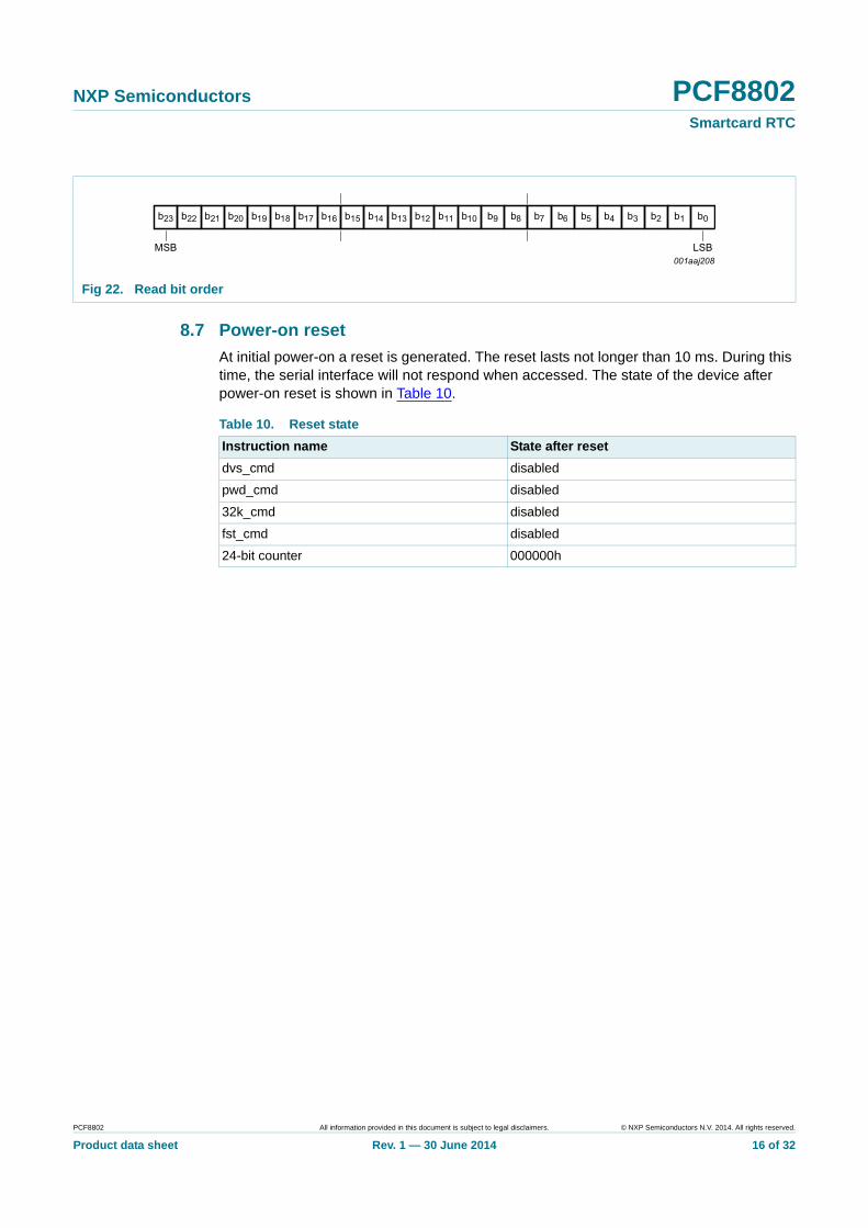
8.5.3 Bit order
Data is transferred MSB first.
8.5.4 START and STOP conditions
Both data and clock lines remain HIGH when the bus is not busy. A HIGH-to-LOW transition of the data line, while the clock is HIGH is defined as the START condition (S). A LOW-to-HIGH transition of the data line while the clock is HIGH is defined as the STOP condition (P). The START and STOP conditions are shown in Figure 12.
The data on SDA is sampled with the rising edge of SCL. Data is output to SDA on the falling edge of SCL.
8.5.5 System configuration
A device generating a message is a transmitter, a device receiving a message is the receiver. The device that controls the message is the master and the device which is controlled by the master is the slave.
8.5.6 Acknowledge
The number of data bytes transferred between the START and STOP conditions from transmitter to receiver is unlimited. But the duration of the access must not exceed 32 seconds. Each byte of 8 bits is followed by an acknowledge bit. The acknowledge bit is a HIGH level signal put on the bus by the transmitter during which time the master generates an extra acknowledge related clock pulse. A slave receiver which is addressed must generate an acknowledge after the reception of each byte. Also a master receiver must generate an acknowledge after the reception of each byte that has been clocked out of the slave transmitter. The device that acknowledges must pull-down the SDA line during the acknowledge clock pulse, so that the SDA line is stable LOW during the HIGH period of the acknowledge related clock pulse (set-up and hold times must be considered). A master receiver must signal an end of data to the transmitter by not generating an acknowledge on the last byte that has been clocked out of the slave. In this event, the transmitter must leave the data line HIGH to enable the master to generate a STOP condition. Acknowledgement is shown in Figure 13.
Fig 11. Bit transfer
Fig 12. Definition of START and STOP conditions
PCF8802 All information provided in this document is subject to legal disclaimers. © NXP Semiconductors N.V. 2014. All rights reserved.
Product data sheet Rev. 1 — 30 June 2014 9 of 32

NXP Semiconductors PCF8802Smartcard RTC
8.5.7 Data transfer
Fig 13. Acknowledgement on the I2C-bus
Fig 14. A complete data transfer
Fig 15. A master-transmitter addresses a slave receiver
Fig 16. A master reads from a slave immediately after the first byte
PCF8802 All information provided in this document is subject to legal disclaimers. © NXP Semiconductors N.V. 2014. All rights reserved.
Product data sheet Rev. 1 — 30 June 2014 10 of 32

NXP Semiconductors PCF8802Smartcard RTC
8.5.7.1 Example data transfers
Example 1: Sending the instruction dvs_cmd followed by fst_cmd is shown in Figure 18.
Example 2: Sending dvs_cmd followed by setting the counter to A90001h is shown in Figure 19
Example 3: Reading the counter (counter = 000011h) is shown in Figure 20.
(1) Not shaded because transfer direction of data and acknowledge bits depends on R/W bits.
Fig 17. Combined format
Wrt_cmd is slave address plus write bit.
Fig 18. Sending instructions
Wrt_cmd is slave address plus write bit.
Fig 19. Setting the counter
PCF8802 All information provided in this document is subject to legal disclaimers. © NXP Semiconductors N.V. 2014. All rights reserved.
Product data sheet Rev. 1 — 30 June 2014 11 of 32

NXP Semiconductors PCF8802Smartcard RTC
8.6 Instructions
8.6.1 Instruction set
Rd_cmd is slave address plus read bit.
Fig 20. Reading the counter
Table 6. Write instructionsThe writing protocol is illustrated in Figure 7.
First byte Second byte Further bytes Action
Instruction Instruction code Instruction Instruction code Parameters
wrt_cmd 1010 0000 - device slave write address: slave address plus write bit
dvs_cmd 0001 0001 - stop and reset dividers
0001 0000 - start dividers
pwd_cmd 0010 0001 - shut down the device
0010 0000 - enable the device
32k_cmd 0011 0001 - enable output of 32.768 kHz on pin INT
0011 0000 - disable output of 32.768 kHz on pin INT
fst_cmd 0100 0001 - fast mode; increments counter every second
0100 0000 - fast mode disable
set_cmd 1000 0000 set the counter value
P1[23:16] parameter with counter values
P2[15:8]
P3[7:0]
PCF8802 All information provided in this document is subject to legal disclaimers. © NXP Semiconductors N.V. 2014. All rights reserved.
Product data sheet Rev. 1 — 30 June 2014 12 of 32

NXP Semiconductors PCF8802Smartcard RTC
[1] Read of the counter is implicit with an interface read.
8.6.2 Instruction wrt_cmd
The write instruction (wrt_cmd) precedes each write sequence. Details of the writing protocol can be found in Section 8.5.1.1.
8.6.3 Instruction dvs_cmd
The divider stop instruction (dvs_cmd) can be used to freeze the divider chain and to put it in a defined state. The first 2 bits of the divider chain cannot be influenced. With this instruction, it is possible to control the time to the next increment of the counter. See Table 9.
When the dividers are restarted, the first increment of the 24-bit counter will be after 32 seconds.
Table 7. Read instructionsThe reading protocol is illustrated in Figure 8.
First byte Further bytes Action
Instruction Instruction code Parameters
rd_cmd[1] 1010 0001 device slave read address: slave address plus read bit
P1[23:16] parameter with counter values;continues to read until no ACK is received; counter is not updated during this time
P2[15:8]
P3[7:0]
P4[23:16]
:
Divider_1 = dividing by 4.
Divider_2 = dividing by 8192.
Divider_3 = dividing by 32.
Fig 21. Instruction dvs_cmd
PCF8802 All information provided in this document is subject to legal disclaimers. © NXP Semiconductors N.V. 2014. All rights reserved.
Product data sheet Rev. 1 — 30 June 2014 13 of 32

NXP Semiconductors PCF8802Smartcard RTC
When the dividers are restarted, the 8192 Hz clock could have just occurred and hence a delay of 1⁄8192 seconds will occur before the next increment of the divider_2. Or the 8192 Hz clock could be just about to occur and immediately increment the divider_2. As a consequence, an uncertainty of one half clock period in the starting of the 24 bit counter is present when restarting (see Figure 21).
8.6.4 Instruction pwd_cmd
The power down instruction (pwd_cmd) is intended to be used to put the system into a low-power mode for storage. Static leakage current will be the only power consumed. Storage at temperatures exceeding room temperature can increase leakage currents.
Entering deep sleep mode requires a specific sequence of events since under normal circumstances stopping the oscillator would result in a chip reset.
8.6.5 Instruction 32k_cmd
The 32.768 kHz enable instruction (32k_cmd) is intended to aid with oscillator characterization during system development. With this instruction, it is possible to obtain a 32.768 kHz clock on the INT pin which can be used for measurement.
This mode does not affect other operation of the chip except for the loss of interrupt output.
8.6.6 Instruction fst_cmd
The fast mode instruction (fst_cmd) is intended to enable faster system development. When enabled, the counter increments once every second instead of once every 32 seconds. Interrupt pulses are generated once every second as well.
Table 8. Deep sleep mode sequence
Step Action Code sequence Note
To enter deep sleep mode
1 initiate transfer START condition -
2 send wrt_cmd 1010 0000 -
3 enable dvs_cmd 0001 0001 stop the divider
4 set counter with set_cmd 1000 0000 set the counter = AAAAAAh
1010 1010 P1[23:16]
1010 1010 P2[15:8]
1010 1010 P3[7:0]
5 enable pwd_cmd 0010 0001 stop the oscillator
6 end transfer STOP condition -
7 device is now in deep sleep mode
- -
To exit deep sleep mode
1 initiate transfer START condition -
2 send wrt_cmd 1010 0000 -
3 disable pwd_cmd 0010 0000 oscillator starts on the ACK cycle of this instruction
4 disable dvs_cmd 0001 0000 enable the divider again
5 end transfer STOP condition -
PCF8802 All information provided in this document is subject to legal disclaimers. © NXP Semiconductors N.V. 2014. All rights reserved.
Product data sheet Rev. 1 — 30 June 2014 14 of 32

NXP Semiconductors PCF8802Smartcard RTC
When using fst_cmd, data access to the device must be completed within 1 second, if not then counter increments are lost. The 1 second period is measured from the ACK cycle of a valid slave address to the next STOP or repeated START. A repeated START is sufficient to allow the counter to increment.
8.6.7 Instruction set_cmd
The counter can be set to any value using the set instruction (set_cmd). Partial writing of the data parameters results in partial setting of the counter. For example, if data transfer is stopped after P1[23:16] is transmitted, then only bit 23 to bit 16 will be updated.
This instruction takes only 3 parameters in one command. Data after the third parameter are interpreted as the next instruction.
Accurate setting and start-up can be implemented using the dvs_cmd instruction in cooperation with the set_cmd instruction. An example is shown in Table 9.
8.6.8 Instruction rd_cmd
With the read instruction (rd_cmd) the counter value can be read at any time. When the counter value is read, the counter is frozen so that there are no changes during the read back. After a read is terminated, the counter will be allowed to increment again. Any increment that was scheduled during the frozen period will then be effected.
Reading the counter is cyclic, that is, the device repeatedly returns the present counter value until the read is terminated. Reading the counter more than once can be useful in the case that the application is subject to a strong Electromagnetic Interference (EMI) environment, so that read-back values can be compared.
Read back must be terminated within 32 seconds else a count will be dropped.
Table 9. Example of accurate setting of the counter
Step Action Code sequence Note
1 initiate transfer START condition -
2 send wrt_cmd 1010 0000 -
3 enable dvs_cmd 0001 0001 -
4 set counter with set_cmd 1000 0000 set the counter = 1
0000 0000 P1[23:16]
0000 0000 P2[15:8]
0000 0001 P3[7:0]
5 end transfer STOP condition -
6 wait for an external time marker
- -
7 initiate transfer START condition -
8 send wrt_cmd 1010 0000 -
9 disable dvs_cmd 0001 0000 counter starts on the ACK cycle of this instruction
10 end transfer STOP condition -
PCF8802 All information provided in this document is subject to legal disclaimers. © NXP Semiconductors N.V. 2014. All rights reserved.
Product data sheet Rev. 1 — 30 June 2014 15 of 32
NXP Semiconductors PCF8802Smartcard RTC
8.7 Power-on reset
At initial power-on a reset is generated. The reset lasts not longer than 10 ms. During this time, the serial interface will not respond when accessed. The state of the device after power-on reset is shown in Table 10.
Fig 22. Read bit order
Table 10. Reset state
Instruction name State after reset
dvs_cmd disabled
pwd_cmd disabled
32k_cmd disabled
fst_cmd disabled
24-bit counter 000000h
PCF8802 All information provided in this document is subject to legal disclaimers. © NXP Semiconductors N.V. 2014. All rights reserved.
Product data sheet Rev. 1 — 30 June 2014 16 of 32

NXP Semiconductors PCF8802Smartcard RTC
9. Internal circuitry
10. Safety notes
Fig 23. Diode protection diagram
CAUTION
This device is sensitive to ElectroStatic Discharge (ESD). Observe precautions for handling electrostatic sensitive devices.
Such precautions are described in the ANSI/ESD S20.20, IEC/ST 61340-5, JESD625-A or equivalent standards.
CAUTION
Semiconductors are light sensitive. Exposure to light sources can cause the IC to malfunction. The IC must be protected against light. The protection must be applied to all sides of the IC.
PCF8802 All information provided in this document is subject to legal disclaimers. © NXP Semiconductors N.V. 2014. All rights reserved.
Product data sheet Rev. 1 — 30 June 2014 17 of 32

NXP Semiconductors PCF8802Smartcard RTC
11. Limiting values
[1] Pass level; Human Body Model (HBM) according to JESD22-A114.
[2] Pass level; Machine Model (MM), according to JESD22-A115.
[3] Pass level; Latch-up testing, according to JESD78.
[4] According to the store and transport requirements (see Ref. 11 “UM10569”) the devices have to be stored at a temperature of +8 C to +45 C and a humidity of 25 % to 75 %.
Table 11. Limiting valuesIn accordance with the Absolute Maximum Rating System (IEC 60134).
Symbol Parameter Conditions Min Max Unit
VDD supply voltage 0.5 +6.5 V
IDD supply current 50 +50 mA
VI input voltage 0.5 +6.5 V
II input current 10 +10 mA
VO output voltage 0.5 +6.5 V
IO output current 10 +10 mA
Ptot total power dissipation - 300 mW
Vesd electrostatic discharge voltage
HBM [1] - 2500 V
MM [2] - 200 V
Ilu latch-up current [3] - 200 mA
Tamb ambient temperature 40 +85 C
Tstg storage temperature [4] 65 +150 C
PCF8802 All information provided in this document is subject to legal disclaimers. © NXP Semiconductors N.V. 2014. All rights reserved.
Product data sheet Rev. 1 — 30 June 2014 18 of 32

NXP Semiconductors PCF8802Smartcard RTC
12. Static characteristics
Table 12. Static characteristicsVDD = 1.6 V to 5.5 V; VSS = 0 V; fosc = 32.768 kHz; Tamb = 40 C to +85 C; quartz crystal: Rs = 30 k, CL = 6.0 pF; unless otherwise specified.
Symbol Parameter Conditions Min Typ Max Unit
Supplies
VDD supply voltage 1.6 - 5.5 V
Tamb = 25 C;fSCL = 0 Hz
- 1.0 - V
VDD supply voltage variation
V/t = 1 V/s - 0.25 - V
IDD supply current deep sleep active [1]
Tamb = 25 C;VDD = 3 V;fSCL = 0 Hz
- 3 - nA
device running
fSCL = 0 Hz - - 400 nA
Tamb = 25 C;VDD = 3 V;fSCL = 0 Hz
- 130 - nA
interface active
fSCL = 100 kHz - 5 20 A
fSCL = 1 MHz - 50 100 A
Oscillator
Vstart start voltage - 1.1 - V
tstartup start-up time - 0.2 - s
CL(itg) integrated load capacitance
[2] - 6.0 - pF
Inputs
VIL LOW-level input voltage
- - 0.3VDD V
VIH HIGH-level input voltage
0.7VDD - - V
VI input voltage on pins SCL, OSCI, TEST 0.5 - 5.5 V
on pin SDA 0.5 - VDD + 0.5 V
ILI input leakage current VI = VDD or VSS;on pins SCL, SDA and TEST
200 0 +200 nA
Outputs
VO output voltage 0.5 - VDD+0.5 V
IOH HIGH-level output current
VOH = 4.0 V;VDD = 5 V;on pins INT and SDA
- 5 2 mA
VOH = 1.28 V;VDD = 1.6 V;on pins INT and SDA
- 0.5 0.2 mA
PCF8802 All information provided in this document is subject to legal disclaimers. © NXP Semiconductors N.V. 2014. All rights reserved.
Product data sheet Rev. 1 — 30 June 2014 19 of 32

NXP Semiconductors PCF8802Smartcard RTC
[1] Unless otherwise defined, IDD is measured with the reset state, see Section 8.7.
[2] Integrated load capacitance, CL(itg), is a calculation of COSCI and COSCO in series: .
IOL LOW-level output current
VOL = 1.0 V;VDD = 5 V;on pins INT and SDA
2 7 - mA
VOL = 0.32 V;VDD = 1.6 V;on pins INT and SDA
0.4 1 - mA
ILO output leakage current VO = VDD or VSS;on pins SDA and INT
200 0 +200 nA
Table 12. Static characteristics …continuedVDD = 1.6 V to 5.5 V; VSS = 0 V; fosc = 32.768 kHz; Tamb = 40 C to +85 C; quartz crystal: Rs = 30 k, CL = 6.0 pF; unless otherwise specified.
Symbol Parameter Conditions Min Typ Max Unit
CL itg COSCI COSCO COSCI COSCO+
--------------------------------------------=
PCF8802 All information provided in this document is subject to legal disclaimers. © NXP Semiconductors N.V. 2014. All rights reserved.
Product data sheet Rev. 1 — 30 June 2014 20 of 32

NXP Semiconductors PCF8802Smartcard RTC
13. Dynamic characteristics
[1] All timing values are valid within the operating supply voltage and ambient temperature range and are referenced to VIL and VIH with an input voltage swing of VSS to VDD.
[2] Rise and fall times are not limited. Fast edges can lead to system EMI problems, while slow edges are susceptible to noise.
Table 13. Dynamic characteristicsVDD = 1.6 V to 5.5 V; VSS = 0 V; Tamb = 40 C to +85 C; unless otherwise specified. [1]
Symbol Parameter Conditions Min Typ Max Unit
Timing characteristics: serial bus
fSCL SCL clock frequency - - 1 MHz
tLOW LOW period of the SCL clock
500 - - ns
tHIGH HIGH period of the SCL clock
260 - - ns
tBUF bus free time between a STOP and START condition
500 - - ns
tHD;STA hold time (repeated) START condition
260 - - ns
tSU;STA set-up time for a repeated START condition
260 - - ns
tr rise time of both SDA and SCL signals
[2] - 10 - ns
tf fall time of both SDA and SCL signals
[2] - 10 - ns
tSU;DAT data set-up time 50 - - ns
tHD;DAT data hold time 0 - - ns
tSU;STO set-up time for STOP condition
260 - - ns
tVD;DAT data valid time 75 - 450 ns
Cb capacitive load for each bus line
- - 50 pF
Timing characteristics: INT
tw(int) interrupt pulse width 20 40 80 s
PCF8802 All information provided in this document is subject to legal disclaimers. © NXP Semiconductors N.V. 2014. All rights reserved.
Product data sheet Rev. 1 — 30 June 2014 21 of 32

NXP Semiconductors PCF8802Smartcard RTC
Fig 24. Serial bus timing waveforms
Fig 25. INT timing
PCF8802 All information provided in this document is subject to legal disclaimers. © NXP Semiconductors N.V. 2014. All rights reserved.
Product data sheet Rev. 1 — 30 June 2014 22 of 32

NXP Semiconductors PCF8802Smartcard RTC
14. Bare die outline
[1] Including saw lane.
[2] Pad size.
[3] Bump size.
Fig 26. Bare die outline PCF8802AUG
Table 14. Dimensions of PCF8802AUGOriginal dimensions are in mm.
Unit (mm) A A1 D[1] E[1] e e1 e2 P1[2] P2
[3] P3[2] P4
[3]
max - 0.018 - - - - - - 0.093 - 0.093
nom 0.215 0.015 1.19 1.14 0.396 0.448 0.449 0.099 0.090 0.099 0.090
min - 0.012 - - - - - - 0.087 - 0.087
PCF8802 All information provided in this document is subject to legal disclaimers. © NXP Semiconductors N.V. 2014. All rights reserved.
Product data sheet Rev. 1 — 30 June 2014 23 of 32

NXP Semiconductors PCF8802Smartcard RTC
[1] All coordinates are referenced, in m, to the center of the die (see Figure 26).
[2] The substrate (rear side of the die) is connected to VSS and should be electrically isolated.
[3] Die size before dicing. Final dimensions will be 10 m to 20 m smaller.
[1] Pressure of diamond head: 10 g to 50 g.
15. Handling information
All input and output pins are protected against ElectroStatic Discharge (ESD) under normal handling. When handling Metal-Oxide Semiconductor (MOS) devices ensure that all normal precautions are taken as described in JESD625-A, IEC 61340-5 or equivalent standards.
Pin 1 is identified by this symbol.
Fig 27. Pin 1 identifier
Table 15. Bump and reference point locations of PCF8802AUG
Symbol Pad Coordinates[1]
x y
INT 1 437 396
VDD 2 12 430
TEST 3 460 396
OSCO 4 460 1
OSCI 5 460 396
VSS[2] 6 12 430
SCL 7 437 396
SDA 8 437 1
pin 1 identifier - 474.7 472.0
bottom left die corner[3] - 594.8 568.2
top right die corner[3] - 594.7 568.3
Table 16. Gold bump hardness of PCF8802AUG
Gold bump type Min Max Unit[1]
soft gold bump 35 80 HV
PCF8802 All information provided in this document is subject to legal disclaimers. © NXP Semiconductors N.V. 2014. All rights reserved.
Product data sheet Rev. 1 — 30 June 2014 24 of 32
NXP Semiconductors PCF8802Smartcard RTC
16. Packing information
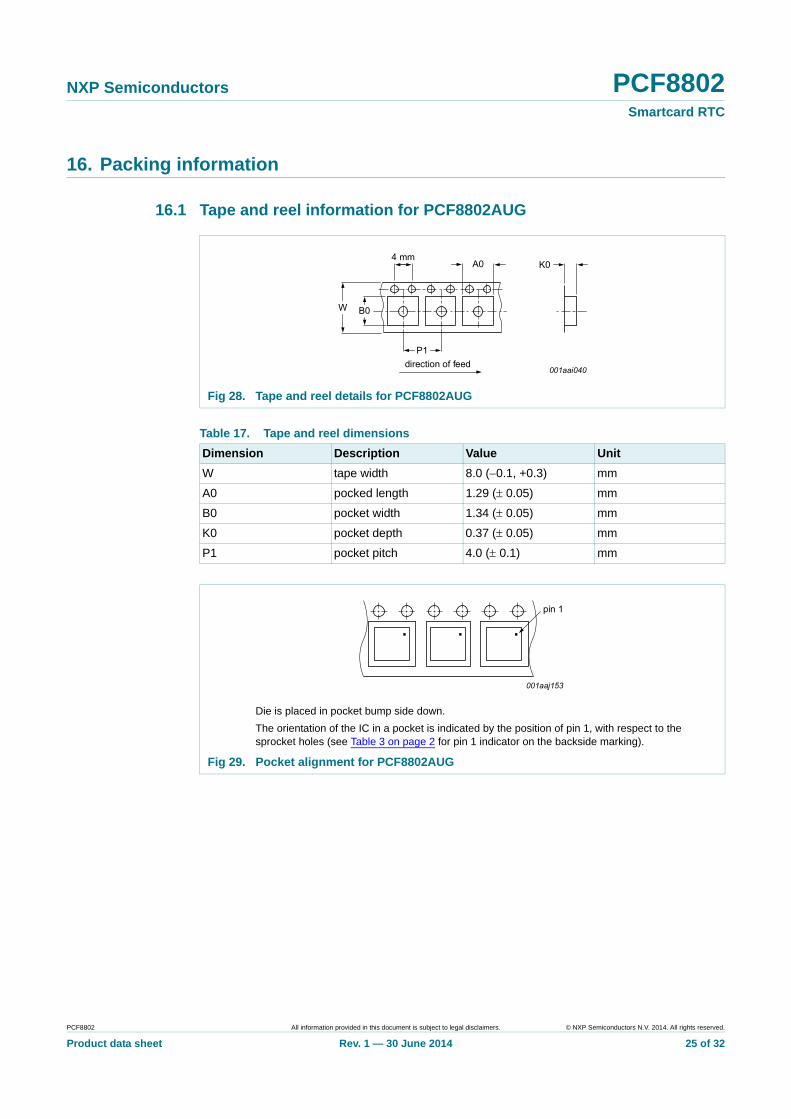
16.1 Tape and reel information for PCF8802AUG
Fig 28. Tape and reel details for PCF8802AUG
Table 17. Tape and reel dimensions
Dimension Description Value Unit
W tape width 8.0 (0.1, +0.3) mm
A0 pocked length 1.29 ( 0.05) mm
B0 pocket width 1.34 ( 0.05) mm
K0 pocket depth 0.37 ( 0.05) mm
P1 pocket pitch 4.0 ( 0.1) mm
Die is placed in pocket bump side down.
The orientation of the IC in a pocket is indicated by the position of pin 1, with respect to the sprocket holes (see Table 3 on page 2 for pin 1 indicator on the backside marking).
Fig 29. Pocket alignment for PCF8802AUG
PCF8802 All information provided in this document is subject to legal disclaimers. © NXP Semiconductors N.V. 2014. All rights reserved.
Product data sheet Rev. 1 — 30 June 2014 25 of 32

NXP Semiconductors PCF8802Smartcard RTC
17. Abbreviations
18. References
[1] AN10439 — Wafer Level Chip Size Package
[2] AN10706 — Handling bare die
[3] AN10853 — ESD and EMC sensitivity of IC
[4] IEC 60134 — Rating systems for electronic tubes and valves and analogous semiconductor devices
[5] IEC 61340-5 — Protection of electronic devices from electrostatic phenomena
[6] JESD22-A114 — Electrostatic Discharge (ESD) Sensitivity Testing Human Body Model (HBM)
[7] JESD22-A115 — Electrostatic Discharge (ESD) Sensitivity Testing Machine Model (MM)
[8] JESD78 — IC Latch-Up Test
[9] JESD625-A — Requirements for Handling Electrostatic-Discharge-Sensitive (ESDS) Devices
[10] UM10204 — I2C-bus specification and user manual
[11] UM10569 — Store and transport requirements
Table 18. Abbreviations
Acronym Description
CMOS Complementary Metal Oxide Semiconductor
EMI ElectroMagnetic Interference
HBM Human Body Model
IC Integrated Circuit
LCD Liquid Crystal Display
LSB Least Significant Bit
MM Machine Model
MSB Most Significant Bit
PCB Printed-Circuit Board
RTC Real-Time Clock
WLCSP Wafer Level Chip-Size Package
PCF8802 All information provided in this document is subject to legal disclaimers. © NXP Semiconductors N.V. 2014. All rights reserved.
Product data sheet Rev. 1 — 30 June 2014 26 of 32

NXP Semiconductors PCF8802Smartcard RTC
19. Revision history
Table 19. Revision history
Document ID Release date Data sheet status Change notice Supersedes
PCF8802 v.1 20140630 Product data sheet - -
PCF8802 All information provided in this document is subject to legal disclaimers. © NXP Semiconductors N.V. 2014. All rights reserved.
Product data sheet Rev. 1 — 30 June 2014 27 of 32
NXP Semiconductors PCF8802Smartcard RTC
20. Legal information
20.1 Data sheet status
[1] Please consult the most recently issued document before initiating or completing a design.
[2] The term ‘short data sheet’ is explained in section “Definitions”.
[3] The product status of device(s) described in this document may have changed since this document was published and may differ in case of multiple devices. The latest product status information is available on the Internet at URL http://www.nxp.com.
20.2 Definitions
Draft — The document is a draft version only. The content is still under internal review and subject to formal approval, which may result in modifications or additions. NXP Semiconductors does not give any representations or warranties as to the accuracy or completeness of information included herein and shall have no liability for the consequences of use of such information.
Short data sheet — A short data sheet is an extract from a full data sheet with the same product type number(s) and title. A short data sheet is intended for quick reference only and should not be relied upon to contain detailed and full information. For detailed and full information see the relevant full data sheet, which is available on request via the local NXP Semiconductors sales office. In case of any inconsistency or conflict with the short data sheet, the full data sheet shall prevail.
Product specification — The information and data provided in a Product data sheet shall define the specification of the product as agreed between NXP Semiconductors and its customer, unless NXP Semiconductors and customer have explicitly agreed otherwise in writing. In no event however, shall an agreement be valid in which the NXP Semiconductors product is deemed to offer functions and qualities beyond those described in the Product data sheet.
20.3 Disclaimers
Limited warranty and liability — Information in this document is believed to be accurate and reliable. However, NXP Semiconductors does not give any representations or warranties, expressed or implied, as to the accuracy or completeness of such information and shall have no liability for the consequences of use of such information. NXP Semiconductors takes no responsibility for the content in this document if provided by an information source outside of NXP Semiconductors.
In no event shall NXP Semiconductors be liable for any indirect, incidental, punitive, special or consequential damages (including - without limitation - lost profits, lost savings, business interruption, costs related to the removal or replacement of any products or rework charges) whether or not such damages are based on tort (including negligence), warranty, breach of contract or any other legal theory.
Notwithstanding any damages that customer might incur for any reason whatsoever, NXP Semiconductors’ aggregate and cumulative liability towards customer for the products described herein shall be limited in accordance with the Terms and conditions of commercial sale of NXP Semiconductors.
Right to make changes — NXP Semiconductors reserves the right to make changes to information published in this document, including without limitation specifications and product descriptions, at any time and without notice. This document supersedes and replaces all information supplied prior to the publication hereof.
Suitability for use — NXP Semiconductors products are not designed, authorized or warranted to be suitable for use in life support, life-critical or safety-critical systems or equipment, nor in applications where failure or malfunction of an NXP Semiconductors product can reasonably be expected to result in personal injury, death or severe property or environmental damage. NXP Semiconductors and its suppliers accept no liability for inclusion and/or use of NXP Semiconductors products in such equipment or applications and therefore such inclusion and/or use is at the customer’s own risk.
Applications — Applications that are described herein for any of these products are for illustrative purposes only. NXP Semiconductors makes no representation or warranty that such applications will be suitable for the specified use without further testing or modification.
Customers are responsible for the design and operation of their applications and products using NXP Semiconductors products, and NXP Semiconductors accepts no liability for any assistance with applications or customer product design. It is customer’s sole responsibility to determine whether the NXP Semiconductors product is suitable and fit for the customer’s applications and products planned, as well as for the planned application and use of customer’s third party customer(s). Customers should provide appropriate design and operating safeguards to minimize the risks associated with their applications and products.
NXP Semiconductors does not accept any liability related to any default, damage, costs or problem which is based on any weakness or default in the customer’s applications or products, or the application or use by customer’s third party customer(s). Customer is responsible for doing all necessary testing for the customer’s applications and products using NXP Semiconductors products in order to avoid a default of the applications and the products or of the application or use by customer’s third party customer(s). NXP does not accept any liability in this respect.
Limiting values — Stress above one or more limiting values (as defined in the Absolute Maximum Ratings System of IEC 60134) will cause permanent damage to the device. Limiting values are stress ratings only and (proper) operation of the device at these or any other conditions above those given in the Recommended operating conditions section (if present) or the Characteristics sections of this document is not warranted. Constant or repeated exposure to limiting values will permanently and irreversibly affect the quality and reliability of the device.
Terms and conditions of commercial sale — NXP Semiconductors products are sold subject to the general terms and conditions of commercial sale, as published at http://www.nxp.com/profile/terms, unless otherwise agreed in a valid written individual agreement. In case an individual agreement is concluded only the terms and conditions of the respective agreement shall apply. NXP Semiconductors hereby expressly objects to applying the customer’s general terms and conditions with regard to the purchase of NXP Semiconductors products by customer.
No offer to sell or license — Nothing in this document may be interpreted or construed as an offer to sell products that is open for acceptance or the grant, conveyance or implication of any license under any copyrights, patents or other industrial or intellectual property rights.
Document status[1][2] Product status[3] Definition
Objective [short] data sheet Development This document contains data from the objective specification for product development.
Preliminary [short] data sheet Qualification This document contains data from the preliminary specification.
Product [short] data sheet Production This document contains the product specification.
PCF8802 All information provided in this document is subject to legal disclaimers. © NXP Semiconductors N.V. 2014. All rights reserved.
Product data sheet Rev. 1 — 30 June 2014 28 of 32

NXP Semiconductors PCF8802Smartcard RTC
Export control — This document as well as the item(s) described herein may be subject to export control regulations. Export might require a prior authorization from competent authorities.
Non-automotive qualified products — Unless this data sheet expressly states that this specific NXP Semiconductors product is automotive qualified, the product is not suitable for automotive use. It is neither qualified nor tested in accordance with automotive testing or application requirements. NXP Semiconductors accepts no liability for inclusion and/or use of non-automotive qualified products in automotive equipment or applications.
In the event that customer uses the product for design-in and use in automotive applications to automotive specifications and standards, customer (a) shall use the product without NXP Semiconductors’ warranty of the product for such automotive applications, use and specifications, and (b) whenever customer uses the product for automotive applications beyond NXP Semiconductors’ specifications such use shall be solely at customer’s own risk, and (c) customer fully indemnifies NXP Semiconductors for any liability, damages or failed product claims resulting from customer design and use of the product for automotive applications beyond NXP Semiconductors’ standard warranty and NXP Semiconductors’ product specifications.
Translations — A non-English (translated) version of a document is for reference only. The English version shall prevail in case of any discrepancy between the translated and English versions.
Bare die — All die are tested on compliance with their related technical specifications as stated in this data sheet up to the point of wafer sawing and are handled in accordance with the NXP Semiconductors storage and transportation conditions. If there are data sheet limits not guaranteed, these will be separately indicated in the data sheet. There are no post-packing tests performed on individual die or wafers.
NXP Semiconductors has no control of third party procedures in the sawing, handling, packing or assembly of the die. Accordingly, NXP Semiconductors assumes no liability for device functionality or performance of the die or systems after third party sawing, handling, packing or assembly of the die. It is the responsibility of the customer to test and qualify their application in which the die is used.
All die sales are conditioned upon and subject to the customer entering into a written die sale agreement with NXP Semiconductors through its legal department.
20.4 TrademarksNotice: All referenced brands, product names, service names and trademarks are the property of their respective owners.
I2C-bus — logo is a trademark of NXP Semiconductors N.V.
21. Contact information
For more information, please visit: http://www.nxp.com
For sales office addresses, please send an email to: [email protected]
PCF8802 All information provided in this document is subject to legal disclaimers. © NXP Semiconductors N.V. 2014. All rights reserved.
Product data sheet Rev. 1 — 30 June 2014 29 of 32

NXP Semiconductors PCF8802Smartcard RTC
22. Tables
Table 1. Ordering information. . . . . . . . . . . . . . . . . . . . . .2Table 2. Ordering options . . . . . . . . . . . . . . . . . . . . . . . . .2Table 3. Marking codes . . . . . . . . . . . . . . . . . . . . . . . . . .2Table 4. Pin description for PCF8802. . . . . . . . . . . . . . . .3Table 5. Instruction set overview . . . . . . . . . . . . . . . . . . .4Table 6. Write instructions . . . . . . . . . . . . . . . . . . . . . . .12Table 7. Read instructions . . . . . . . . . . . . . . . . . . . . . . .13Table 8. Deep sleep mode sequence. . . . . . . . . . . . . . .14Table 9. Example of accurate setting of the counter . . .15Table 10. Reset state . . . . . . . . . . . . . . . . . . . . . . . . . . . .16Table 11. Limiting values . . . . . . . . . . . . . . . . . . . . . . . . .18Table 12. Static characteristics . . . . . . . . . . . . . . . . . . . .19Table 13. Dynamic characteristics . . . . . . . . . . . . . . . . . .21Table 14. Dimensions of PCF8802AUG. . . . . . . . . . . . . .23Table 15. Bump and reference point locations of
PCF8802AUG . . . . . . . . . . . . . . . . . . . . . . . . .24Table 16. Gold bump hardness of PCF8802AUG . . . . . .24Table 17. Tape and reel dimensions . . . . . . . . . . . . . . . .25Table 18. Abbreviations . . . . . . . . . . . . . . . . . . . . . . . . . .26Table 19. Revision history . . . . . . . . . . . . . . . . . . . . . . .27a
PCF8802 All information provided in this document is subject to legal disclaimers. © NXP Semiconductors N.V. 2014. All rights reserved.
Product data sheet Rev. 1 — 30 June 2014 30 of 32

NXP Semiconductors PCF8802Smartcard RTC
23. Figures
Fig 1. Block diagram of PCF8802 . . . . . . . . . . . . . . . . . .2Fig 2. Pinning diagram of PCF8802AUG. . . . . . . . . . . . .3Fig 3. IDD with respect to Rs. . . . . . . . . . . . . . . . . . . . . . .5Fig 4. Divider chain . . . . . . . . . . . . . . . . . . . . . . . . . . . . .5Fig 5. Counter behavior during read access . . . . . . . . . .6Fig 6. Pulse generator . . . . . . . . . . . . . . . . . . . . . . . . . . .6Fig 7. Writing protocol . . . . . . . . . . . . . . . . . . . . . . . . . . .7Fig 8. Reading protocol . . . . . . . . . . . . . . . . . . . . . . . . . .8Fig 9. Access restrictions. . . . . . . . . . . . . . . . . . . . . . . . .8Fig 10. Bit transfer . . . . . . . . . . . . . . . . . . . . . . . . . . . . . . .8Fig 11. Bit transfer . . . . . . . . . . . . . . . . . . . . . . . . . . . . . . .9Fig 12. Definition of START and STOP conditions. . . . . . .9Fig 13. Acknowledgement on the I2C-bus . . . . . . . . . . . .10Fig 14. A complete data transfer . . . . . . . . . . . . . . . . . . .10Fig 15. A master-transmitter addresses a slave
receiver . . . . . . . . . . . . . . . . . . . . . . . . . . . . . . . .10Fig 16. A master reads from a slave immediately after
the first byte . . . . . . . . . . . . . . . . . . . . . . . . . . . . .10Fig 17. Combined format . . . . . . . . . . . . . . . . . . . . . . . . . 11Fig 18. Sending instructions . . . . . . . . . . . . . . . . . . . . . . 11Fig 19. Setting the counter. . . . . . . . . . . . . . . . . . . . . . . . 11Fig 20. Reading the counter . . . . . . . . . . . . . . . . . . . . . .12Fig 21. Instruction dvs_cmd. . . . . . . . . . . . . . . . . . . . . . .13Fig 22. Read bit order . . . . . . . . . . . . . . . . . . . . . . . . . . .16Fig 23. Diode protection diagram. . . . . . . . . . . . . . . . . . .17Fig 24. Serial bus timing waveforms . . . . . . . . . . . . . . . .22Fig 25. INT timing . . . . . . . . . . . . . . . . . . . . . . . . . . . . . .22Fig 26. Bare die outline PCF8802AUG . . . . . . . . . . . . . .23Fig 27. Pin 1 identifier . . . . . . . . . . . . . . . . . . . . . . . . . . .24Fig 28. Tape and reel details for PCF8802AUG. . . . . . . .25Fig 29. Pocket alignment for PCF8802AUG . . . . . . . . . .25
PCF8802 All information provided in this document is subject to legal disclaimers. © NXP Semiconductors N.V. 2014. All rights reserved.
Product data sheet Rev. 1 — 30 June 2014 31 of 32

NXP Semiconductors PCF8802Smartcard RTC
24. Contents
1 General description . . . . . . . . . . . . . . . . . . . . . . 1
2 Features and benefits . . . . . . . . . . . . . . . . . . . . 1
3 Applications . . . . . . . . . . . . . . . . . . . . . . . . . . . . 1
4 Ordering information. . . . . . . . . . . . . . . . . . . . . 24.1 Ordering options . . . . . . . . . . . . . . . . . . . . . . . . 2
5 Marking . . . . . . . . . . . . . . . . . . . . . . . . . . . . . . . . 2
6 Block diagram . . . . . . . . . . . . . . . . . . . . . . . . . . 2
7 Pinning information. . . . . . . . . . . . . . . . . . . . . . 37.1 Pinning . . . . . . . . . . . . . . . . . . . . . . . . . . . . . . . 37.2 Pin description . . . . . . . . . . . . . . . . . . . . . . . . . 3
8 Functional description . . . . . . . . . . . . . . . . . . . 48.1 Oscillator. . . . . . . . . . . . . . . . . . . . . . . . . . . . . . 48.1.1 Low-power operation . . . . . . . . . . . . . . . . . . . . 48.1.2 Deep sleep mode . . . . . . . . . . . . . . . . . . . . . . . 58.2 Divider . . . . . . . . . . . . . . . . . . . . . . . . . . . . . . . 58.3 Binary counter . . . . . . . . . . . . . . . . . . . . . . . . . 68.4 Pulse generator . . . . . . . . . . . . . . . . . . . . . . . . 68.5 I2C-bus interface. . . . . . . . . . . . . . . . . . . . . . . . 78.5.1 Interface protocol . . . . . . . . . . . . . . . . . . . . . . . 78.5.1.1 The writing protocol . . . . . . . . . . . . . . . . . . . . . 78.5.1.2 The reading protocol. . . . . . . . . . . . . . . . . . . . . 88.5.1.3 Reading and writing limitations . . . . . . . . . . . . . 88.5.2 Bit transfer . . . . . . . . . . . . . . . . . . . . . . . . . . . . 88.5.3 Bit order . . . . . . . . . . . . . . . . . . . . . . . . . . . . . . 98.5.4 START and STOP conditions . . . . . . . . . . . . . . 98.5.5 System configuration . . . . . . . . . . . . . . . . . . . . 98.5.6 Acknowledge . . . . . . . . . . . . . . . . . . . . . . . . . . 98.5.7 Data transfer . . . . . . . . . . . . . . . . . . . . . . . . . . 108.5.7.1 Example data transfers. . . . . . . . . . . . . . . . . . 118.6 Instructions . . . . . . . . . . . . . . . . . . . . . . . . . . . 128.6.1 Instruction set . . . . . . . . . . . . . . . . . . . . . . . . . 128.6.2 Instruction wrt_cmd . . . . . . . . . . . . . . . . . . . . 138.6.3 Instruction dvs_cmd . . . . . . . . . . . . . . . . . . . . 138.6.4 Instruction pwd_cmd. . . . . . . . . . . . . . . . . . . . 148.6.5 Instruction 32k_cmd . . . . . . . . . . . . . . . . . . . . 148.6.6 Instruction fst_cmd . . . . . . . . . . . . . . . . . . . . . 148.6.7 Instruction set_cmd . . . . . . . . . . . . . . . . . . . . 158.6.8 Instruction rd_cmd . . . . . . . . . . . . . . . . . . . . . 158.7 Power-on reset . . . . . . . . . . . . . . . . . . . . . . . . 16
9 Internal circuitry. . . . . . . . . . . . . . . . . . . . . . . . 17
10 Safety notes . . . . . . . . . . . . . . . . . . . . . . . . . . . 17
11 Limiting values. . . . . . . . . . . . . . . . . . . . . . . . . 18
12 Static characteristics. . . . . . . . . . . . . . . . . . . . 19
13 Dynamic characteristics . . . . . . . . . . . . . . . . . 21
14 Bare die outline . . . . . . . . . . . . . . . . . . . . . . . . 23
15 Handling information . . . . . . . . . . . . . . . . . . . 24
16 Packing information . . . . . . . . . . . . . . . . . . . . 2516.1 Tape and reel information for PCF8802AUG . 25
17 Abbreviations . . . . . . . . . . . . . . . . . . . . . . . . . 26
18 References. . . . . . . . . . . . . . . . . . . . . . . . . . . . 26
19 Revision history . . . . . . . . . . . . . . . . . . . . . . . 27
20 Legal information . . . . . . . . . . . . . . . . . . . . . . 2820.1 Data sheet status . . . . . . . . . . . . . . . . . . . . . . 2820.2 Definitions . . . . . . . . . . . . . . . . . . . . . . . . . . . 2820.3 Disclaimers . . . . . . . . . . . . . . . . . . . . . . . . . . 2820.4 Trademarks . . . . . . . . . . . . . . . . . . . . . . . . . . 29
21 Contact information . . . . . . . . . . . . . . . . . . . . 29
22 Tables . . . . . . . . . . . . . . . . . . . . . . . . . . . . . . . . 30
23 Figures . . . . . . . . . . . . . . . . . . . . . . . . . . . . . . . 31
24 Contents. . . . . . . . . . . . . . . . . . . . . . . . . . . . . . 32
© NXP Semiconductors N.V. 2014. All rights reserved.
For more information, please visit: http://www.nxp.comFor sales office addresses, please send an email to: [email protected]
Date of release: 30 June 2014
Document identifier: PCF8802
Please be aware that important notices concerning this document and the product(s)described herein, have been included in section ‘Legal information’.