Embed Size (px)
Citation preview
© 2019 NXP B.V.
PCIe Certification Guide for i.MX8 Serials
1. Introduction This document provides a description of procedures, tools, and criteria for the PCI Express (PCIe) Gen1,2, and 3 Electrical Compliance test for i.MX 8 Serials.
NXP Semiconductors Document Number: AN12444
Application Note Rev.0 , 05/2019
Contents
1. Introduction ........................................................................ 1 2. Test equipment ................................................................... 2
2.1. Test board ................................................................ 2 2.2. Measurement equipment ......................................... 2 2.3. Test environment ..................................................... 5 2.4. Analysis software .................................................... 5 2.5. Additional information ............................................ 5
3. PCIe test procedure ............................................................. 6 4. PCIe test results ................................................................ 13
4.1. PCIe 1.1 test results ............................................... 13 4.2. PCIe 2.0 test results ............................................... 13 4.3. PCIe 3.0 test results ............................................... 14
5. Useful links....................................................................... 15
Test equipment
PCIe Certification Guide for i.MX8 Serials, Application Note, Rev.0, 05/2019 2 NXP Semiconductors
2. Test equipment
2.1. Test board The test is performed on the following boards:
• MCIMX8QXP (As an example)
• MCIMX8QM
• MCIMX8M
• MCIMX8M Mini
2.2. Measurement equipment The following equipment is used to measure signal quality:
• Oscilloscope: Keysight DSAV204A
• Cables & Adapters:
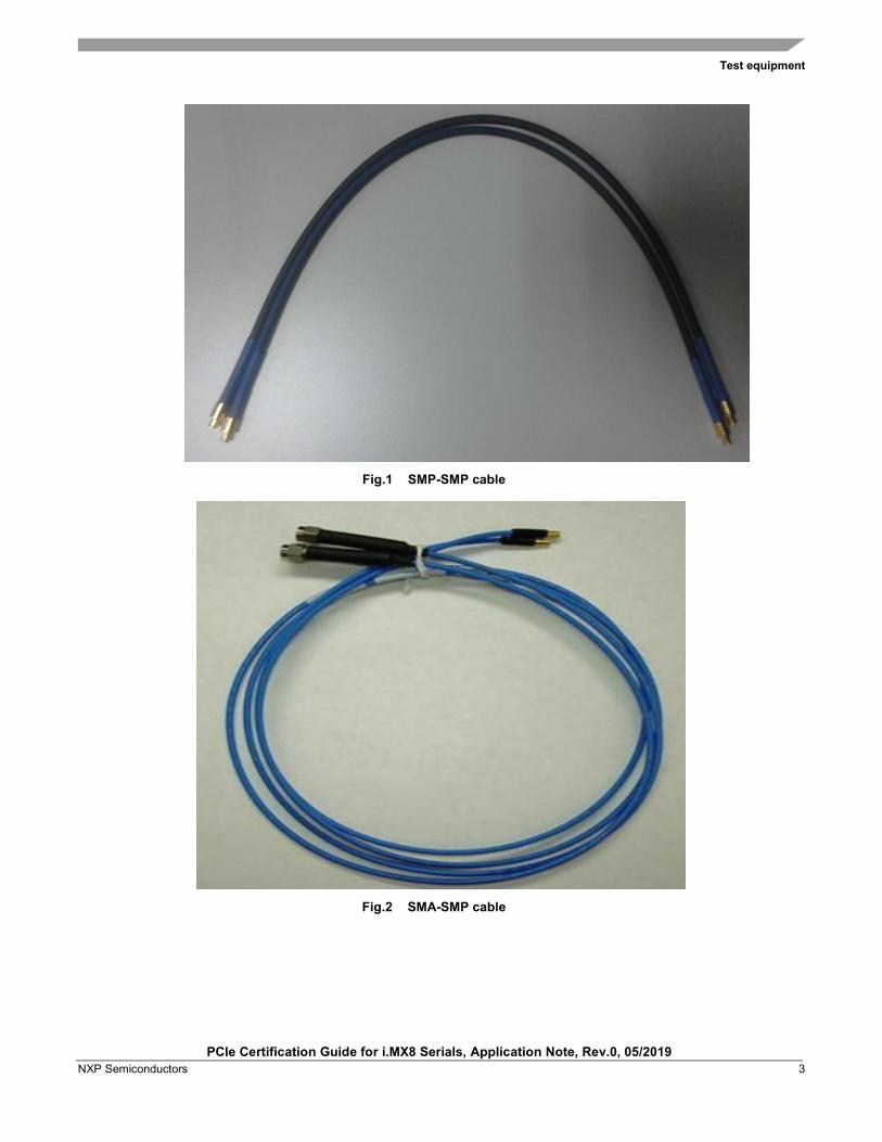
2 Rosenberger SMP-SMP cables P/N: 71L-19K2-19K2-00305C (See Fig.1)
4 Agilent SMA-SMP cables P/N: N4235-61602(See Fig.2)
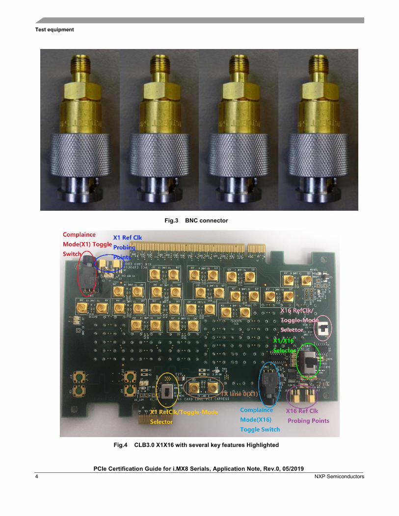
4 Agilent BNC connectors P/N:54855-67604(See Fig.3)
• Test Fixture: CLB3.0 X1/X16(See Fig.4)
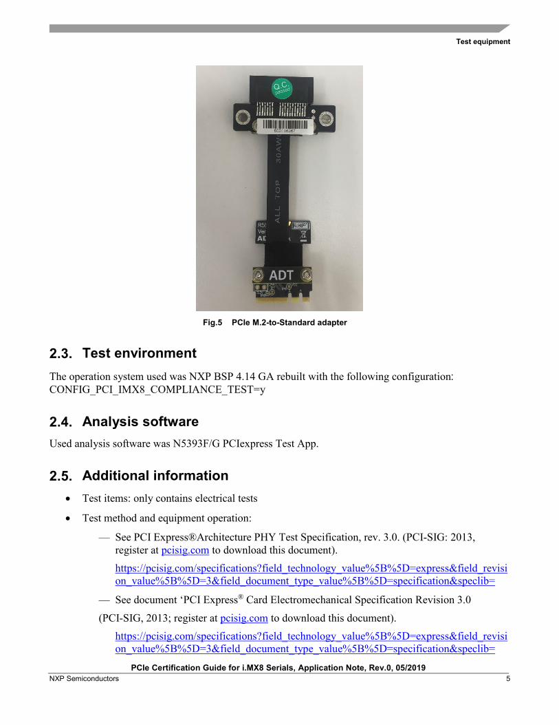
• PCIe M.2-to-Standard adapter you have prepared yourself(See Fig.5)
Test equipment
PCIe Certification Guide for i.MX8 Serials, Application Note, Rev.0, 05/2019 NXP Semiconductors 3
Fig.1 SMP-SMP cable
Fig.2 SMA-SMP cable
Test equipment
PCIe Certification Guide for i.MX8 Serials, Application Note, Rev.0, 05/2019 4 NXP Semiconductors
Fig.3 BNC connector
Fig.4 CLB3.0 X1X16 with several key features Highlighted
Test equipment
PCIe Certification Guide for i.MX8 Serials, Application Note, Rev.0, 05/2019 NXP Semiconductors 5
Fig.5 PCIe M.2-to-Standard adapter
2.3. Test environment The operation system used was NXP BSP 4.14 GA rebuilt with the following configuration: CONFIG_PCI_IMX8_COMPLIANCE_TEST=y
2.4. Analysis software Used analysis software was N5393F/G PCIexpress Test App.
2.5. Additional information • Test items: only contains electrical tests
• Test method and equipment operation:
— See PCI Express®Architecture PHY Test Specification, rev. 3.0. (PCI-SIG: 2013, register at pcisig.com to download this document). https://pcisig.com/specifications?field_technology_value%5B%5D=express&field_revision_value%5B%5D=3&field_document_type_value%5B%5D=specification&speclib=
— See document ‘PCI Express® Card Electromechanical Specification Revision 3.0
(PCI-SIG, 2013; register at pcisig.com to download this document). https://pcisig.com/specifications?field_technology_value%5B%5D=express&field_revision_value%5B%5D=3&field_document_type_value%5B%5D=specification&speclib=
PCIe test procedure
PCIe Certification Guide for i.MX8 Serials, Application Note, Rev.0, 05/2019 6 NXP Semiconductors
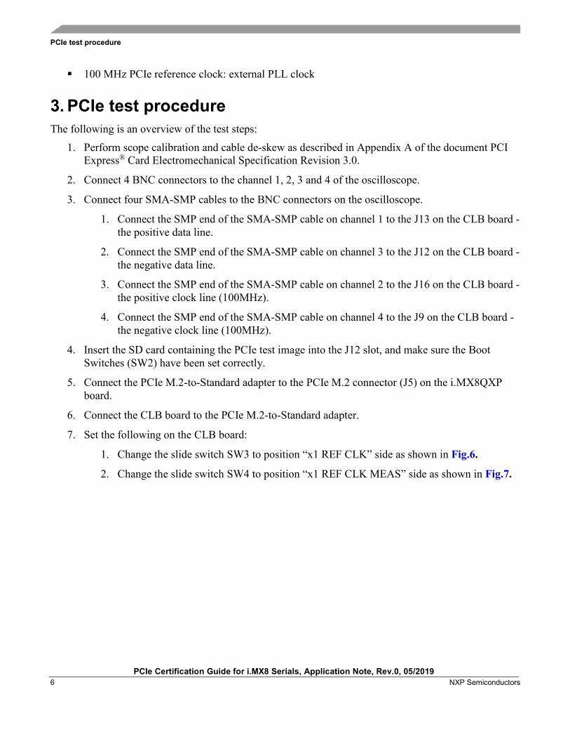
100 MHz PCIe reference clock: external PLL clock
3. PCIe test procedure The following is an overview of the test steps:
1. Perform scope calibration and cable de-skew as described in Appendix A of the document PCI Express® Card Electromechanical Specification Revision 3.0.
2. Connect 4 BNC connectors to the channel 1, 2, 3 and 4 of the oscilloscope.
3. Connect four SMA-SMP cables to the BNC connectors on the oscilloscope.
1. Connect the SMP end of the SMA-SMP cable on channel 1 to the J13 on the CLB board - the positive data line.
2. Connect the SMP end of the SMA-SMP cable on channel 3 to the J12 on the CLB board - the negative data line.
3. Connect the SMP end of the SMA-SMP cable on channel 2 to the J16 on the CLB board -the positive clock line (100MHz).
4. Connect the SMP end of the SMA-SMP cable on channel 4 to the J9 on the CLB board -the negative clock line (100MHz).
4. Insert the SD card containing the PCIe test image into the J12 slot, and make sure the Boot Switches (SW2) have been set correctly.
5. Connect the PCIe M.2-to-Standard adapter to the PCIe M.2 connector (J5) on the i.MX8QXP board.
6. Connect the CLB board to the PCIe M.2-to-Standard adapter.
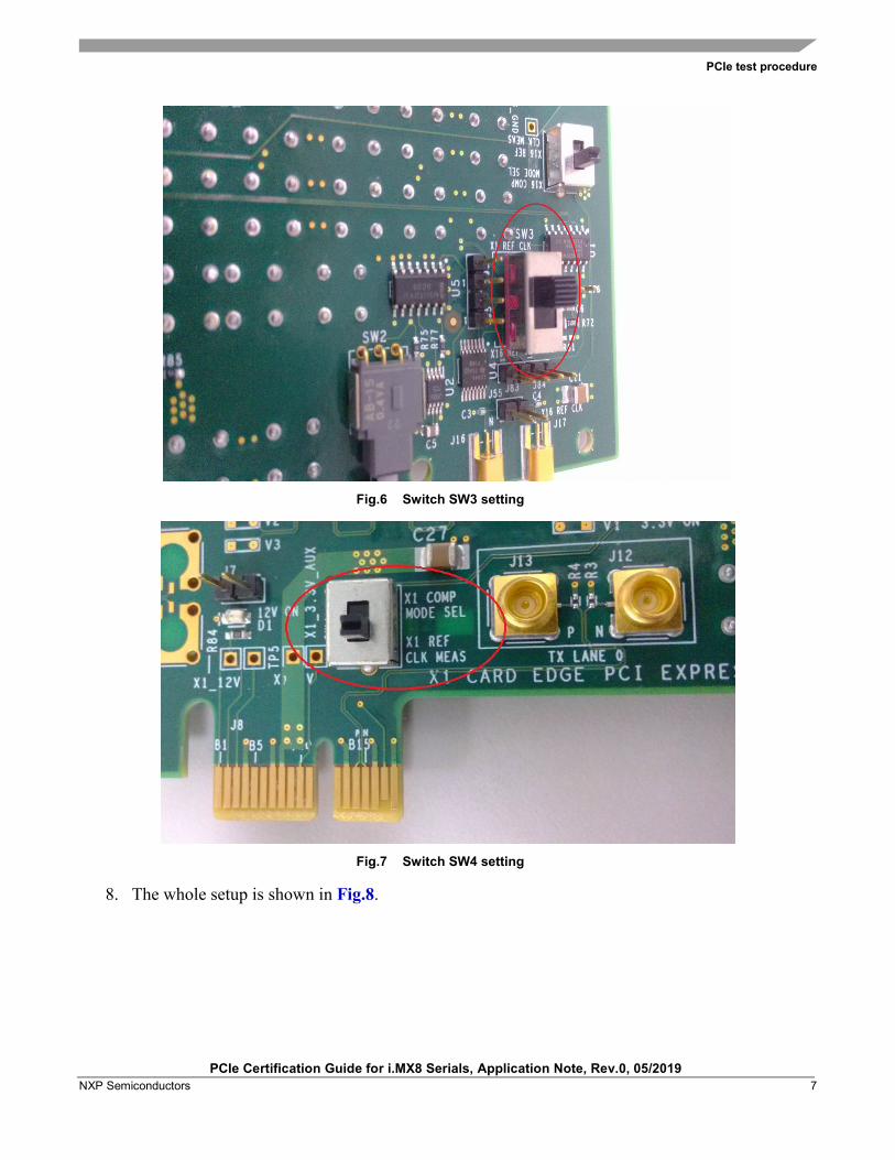
7. Set the following on the CLB board:
1. Change the slide switch SW3 to position “x1 REF CLK” side as shown in Fig.6.
2. Change the slide switch SW4 to position “x1 REF CLK MEAS” side as shown in Fig.7.
PCIe test procedure
PCIe Certification Guide for i.MX8 Serials, Application Note, Rev.0, 05/2019 NXP Semiconductors 7
Fig.6 Switch SW3 setting
Fig.7 Switch SW4 setting
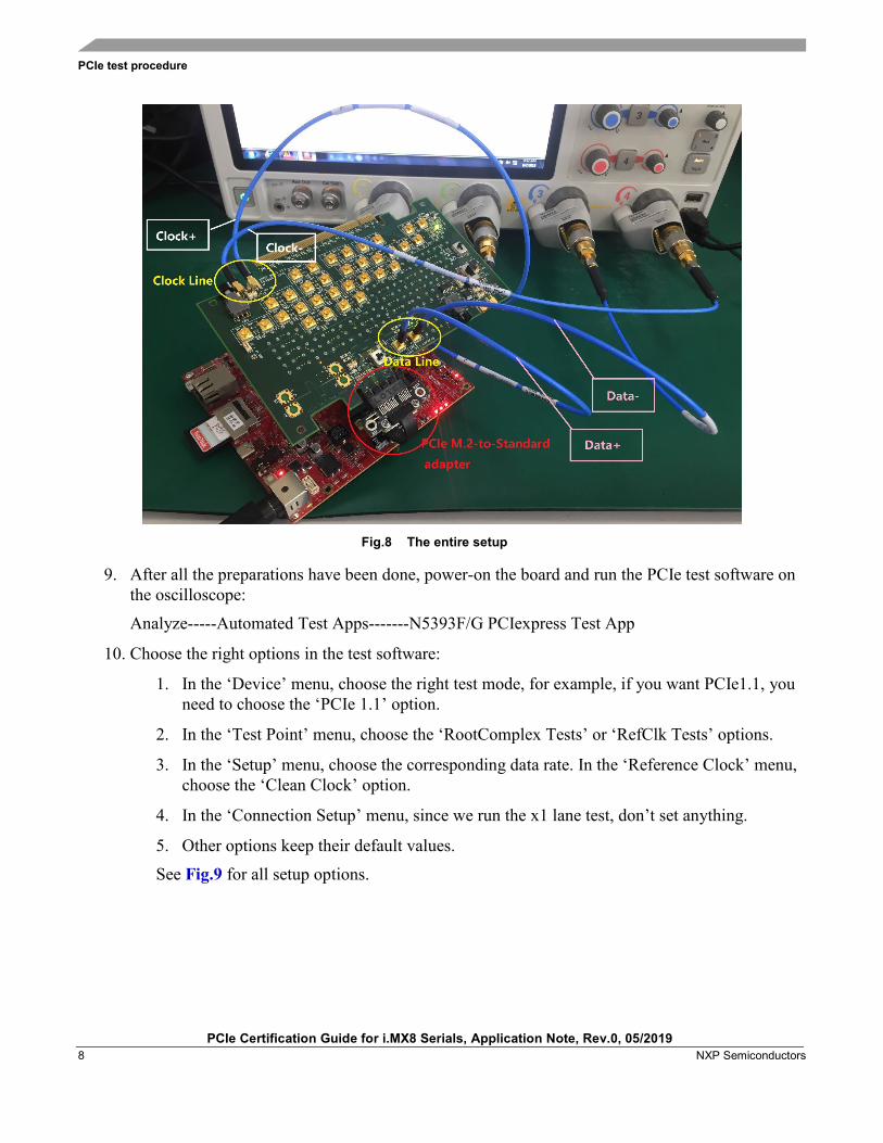
8. The whole setup is shown in Fig.8.
PCIe test procedure
PCIe Certification Guide for i.MX8 Serials, Application Note, Rev.0, 05/2019 8 NXP Semiconductors
Fig.8 The entire setup
9. After all the preparations have been done, power-on the board and run the PCIe test software on the oscilloscope: Analyze-----Automated Test Apps-------N5393F/G PCIexpress Test App
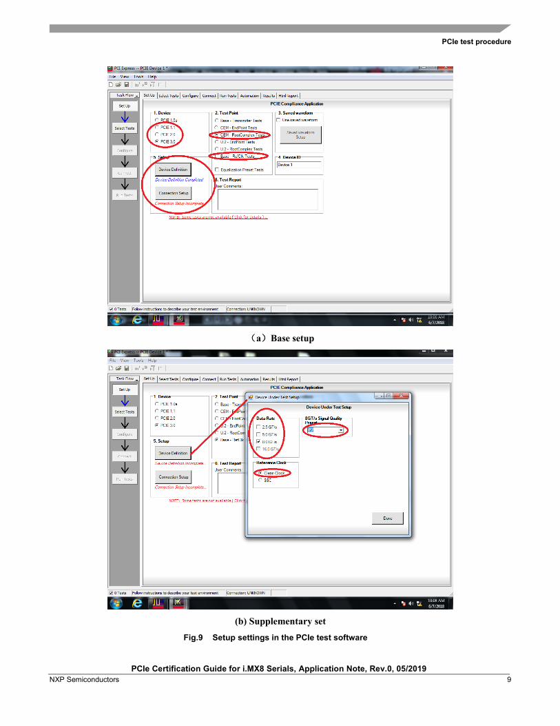
10. Choose the right options in the test software:
1. In the ‘Device’ menu, choose the right test mode, for example, if you want PCIe1.1, you need to choose the ‘PCIe 1.1’ option.
2. In the ‘Test Point’ menu, choose the ‘RootComplex Tests’ or ‘RefClk Tests’ options.
3. In the ‘Setup’ menu, choose the corresponding data rate. In the ‘Reference Clock’ menu, choose the ‘Clean Clock’ option.
4. In the ‘Connection Setup’ menu, since we run the x1 lane test, don’t set anything.
5. Other options keep their default values. See Fig.9 for all setup options.
PCIe test procedure
PCIe Certification Guide for i.MX8 Serials, Application Note, Rev.0, 05/2019 NXP Semiconductors 9
(a)Base setup
(b) Supplementary set
Fig.9 Setup settings in the PCIe test software
PCIe test procedure
PCIe Certification Guide for i.MX8 Serials, Application Note, Rev.0, 05/2019 10 NXP Semiconductors
11. In the ‘Select Tests’ option, choose ‘test all’.
12. In the ‘Connect’ option, based on the reminder to double-check whether the test cables have been connected correctly.
13. If you want to run a PCIe 1.1 test, select ‘Run Tests’ to begin to run the PCIe test.
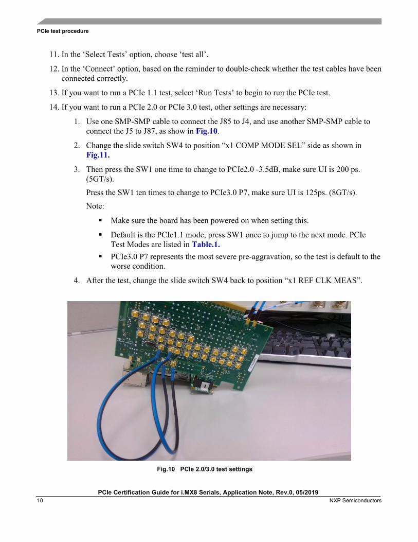
14. If you want to run a PCIe 2.0 or PCIe 3.0 test, other settings are necessary:
1. Use one SMP-SMP cable to connect the J85 to J4, and use another SMP-SMP cable to connect the J5 to J87, as show in Fig.10.
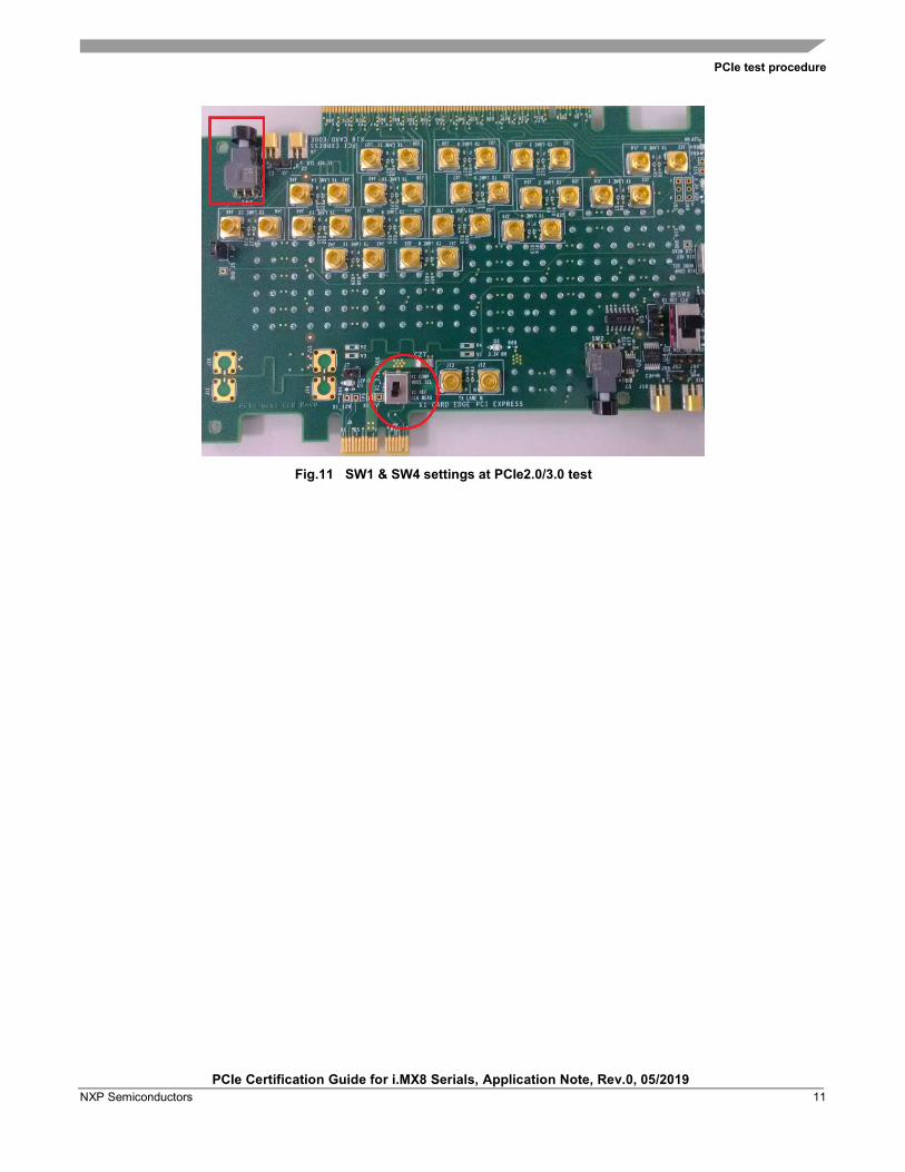
2. Change the slide switch SW4 to position “x1 COMP MODE SEL” side as shown in Fig.11.
3. Then press the SW1 one time to change to PCIe2.0 -3.5dB, make sure UI is 200 ps. (5GT/s). Press the SW1 ten times to change to PCIe3.0 P7, make sure UI is 125ps. (8GT/s). Note:
Make sure the board has been powered on when setting this.
Default is the PCIe1.1 mode, press SW1 once to jump to the next mode. PCIe Test Modes are listed in Table.1.
PCIe3.0 P7 represents the most severe pre-aggravation, so the test is default to the worse condition.
4. After the test, change the slide switch SW4 back to position “x1 REF CLK MEAS”.
Fig.10 PCIe 2.0/3.0 test settings
PCIe test procedure
PCIe Certification Guide for i.MX8 Serials, Application Note, Rev.0, 05/2019 NXP Semiconductors 11
Fig.11 SW1 & SW4 settings at PCIe2.0/3.0 test
PCIe test procedure
PCIe Certification Guide for i.MX8 Serials, Application Note, Rev.0, 05/2019 12 NXP Semiconductors
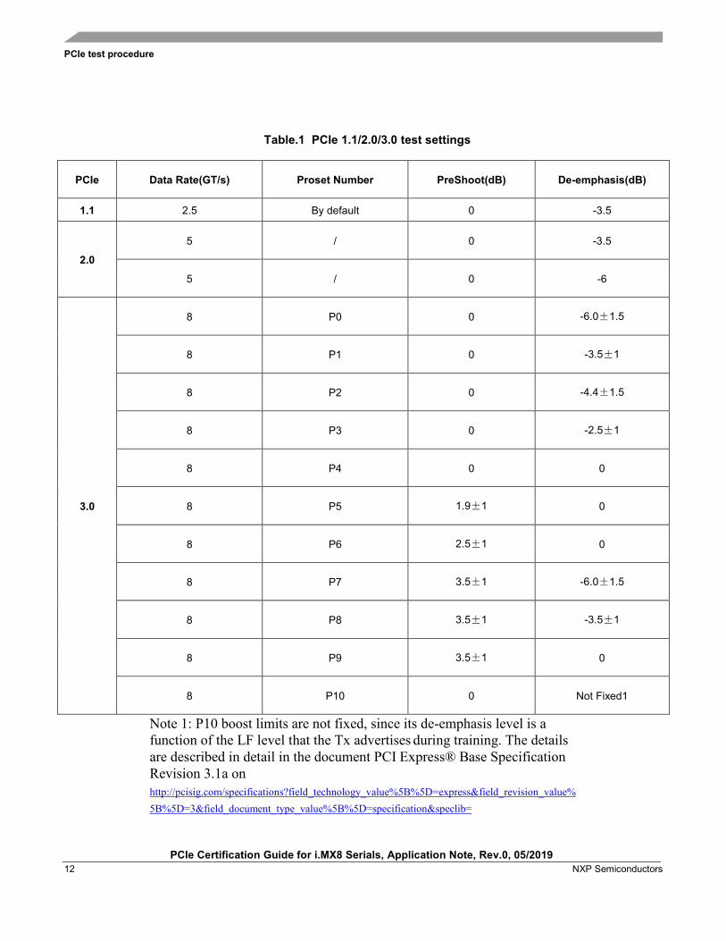
Table.1 PCIe 1.1/2.0/3.0 test settings
PCIe Data Rate(GT/s) Proset Number PreShoot(dB) De-emphasis(dB)
1.1 2.5 By default 0 -3.5
2.0 5 / 0 -3.5
5 / 0 -6
3.0
8 P0 0 -6.0±1.5
8 P1 0 -3.5±1
8 P2 0 -4.4±1.5
8 P3 0 -2.5±1
8 P4 0 0
8 P5 1.9±1 0
8 P6 2.5±1 0
8 P7 3.5±1 -6.0±1.5
8 P8 3.5±1 -3.5±1
8 P9 3.5±1 0
8 P10 0 Not Fixed1
Note 1: P10 boost limits are not fixed, since its de-emphasis level is a function of the LF level that the Tx advertises during training. The details are described in detail in the document PCI Express® Base Specification Revision 3.1a on http://pcisig.com/specifications?field_technology_value%5B%5D=express&field_revision_value%5B%5D=3&field_document_type_value%5B%5D=specification&speclib=
PCIe test results
PCIe Certification Guide for i.MX8 Serials, Application Note, Rev.0, 05/2019 NXP Semiconductors 13
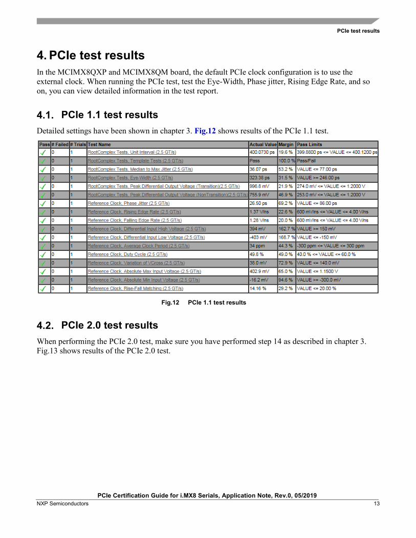
4. PCIe test results In the MCIMX8QXP and MCIMX8QM board, the default PCIe clock configuration is to use the external clock. When running the PCIe test, test the Eye-Width, Phase jitter, Rising Edge Rate, and so on, you can view detailed information in the test report.
4.1. PCIe 1.1 test results Detailed settings have been shown in chapter 3. Fig.12 shows results of the PCIe 1.1 test.
Fig.12 PCIe 1.1 test results
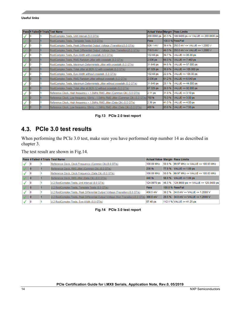
4.2. PCIe 2.0 test results When performing the PCIe 2.0 test, make sure you have performed step 14 as described in chapter 3. Fig.13 shows results of the PCIe 2.0 test.
Useful links
PCIe Certification Guide for i.MX8 Serials, Application Note, Rev.0, 05/2019 14 NXP Semiconductors
Fig.13 PCIe 2.0 test report
4.3. PCIe 3.0 test results When performing the PCIe 3.0 test, make sure you have performed step number 14 as described in chapter 3. The test result are shown in Fig.14.
Fig.14 PCIe 3.0 test report
Useful links
PCIe Certification Guide for i.MX8 Serials, Application Note, Rev.0, 05/2019 NXP Semiconductors 15
5. Useful links • PCI Express Spec
• i.MX 8 Series Applications Processors
• Test software and tools
Document Number: AN12444 Rev.0
05/2019
How to Reach Us:
Home Page: nxp.com
Web Support: nxp.com/support
Information in this document is provided solely to enable system and software implementers to use NXP products. There are no express or implied copyright licenses granted hereunder to design or fabricate any integrated circuits based on the information in this document. NXP reserves the right to make changes without further notice to any products herein.
NXP makes no warranty, representation, or guarantee regarding the suitability of its products for any particular purpose, nor does NXP assume any liability arising out of the application or use of any product or circuit, and specifically disclaims any and all liability, including without limitation consequential or incidental damages. “Typical” parameters that may be provided in NXP data sheets and/or specifications can and do vary in different applications, and actual performance may vary over time. All operating parameters, including “typicals”, must be validated for each customer application by customer’s technical experts. NXP does not convey any license under its patent rights nor the rights of others. NXP sells products pursuant to standard terms and conditions of sale, which can be found at the following address: nxp.com/SalesTermsandConditions.
While NXP has implemented advanced security features, all products may be subject to unidentified vulnerabilities. Customers are responsible for the design and operation of their applications and products to reduce the effect of these vulnerabilities on customer’s applications and products, and NXP accepts no liability for any vulnerability that is discovered. Customers should implement appropriate design and operating safeguards to minimize the risks associated with their applications and products.
NXP, the NXP logo, NXP SECURE CONNECTIONS FOR A SMARTER WORLD, COOLFLUX, EMBRACE, GREENCHIP, HITAG, I2C BUS, ICODE, JCOP, LIFE VIBES, MIFARE, MIFARE CLASSIC, MIFARE DESFire, MIFARE PLUS, MIFARE FLEX, MANTIS, MIFARE ULTRALIGHT, MIFARE4MOBILE, MIGLO, NTAG, ROADLINK, SMARTLX, SMARTMX, STARPLUG, TOPFET, TRENCHMOS, UCODE, Freescale, the Freescale logo, AltiVec, C‑5, CodeTEST, CodeWarrior, ColdFire, ColdFire+, C‑Ware, the Energy Efficient Solutions logo, Kinetis, Layerscape, MagniV, mobileGT, PEG, PowerQUICC, Processor Expert, QorIQ, QorIQ Qonverge, Ready Play, SafeAssure, the SafeAssure logo, StarCore, Symphony, VortiQa, Vybrid, Airfast, BeeKit, BeeStack, CoreNet, Flexis, MXC, Platform in a Package, QUICC Engine, SMARTMOS, Tower, TurboLink, and UMEMS are trademarks of NXP B.V. All other product or service names are the property of their respective owners. AMBA, Arm, Arm7, Arm7TDMI, Arm9, Arm11, Artisan, big.LITTLE, Cordio, CoreLink, CoreSight, Cortex, DesignStart, DynamIQ, Jazelle, Keil, Mali, Mbed, Mbed Enabled, NEON, POP, RealView, SecurCore, Socrates, Thumb, TrustZone, ULINK, ULINK2, ULINK-ME, ULINK-PLUS, ULINKpro, µVision, Versatile are trademarks or registered trademarks of Arm Limited (or its subsidiaries) in the US and/or elsewhere. The related technology may be protected by any or all of patents, copyrights, designs and trade secrets. All rights reserved. Oracle and Java are registered trademarks of Oracle and/or its affiliates. The Power Architecture and Power.org word marks and the Power and Power.org logos and related marks are trademarks and service marks licensed by Power.org.
© 2019 NXP B.V.