Embed Size (px)
Citation preview

www.irf.com © 2008 International Rectifier
1
IRS20957S Protected Digital Audio Driver
Features Floating PWM input enables easy half bridge
implementation
Programmable bidirectional over-current protection with self-reset function
Programmable preset dead-time for improved THD performances
High noise immunity
100V ratings deliver up to 500W in output power
3.3 V/ 5 V logic compatible input
Operates up to 800kHz
Typical Applications Home theatre systems
Mini component stereo systems
Powered speaker systems
General purpose audio power amplifiers
Product Summary
Topology Half-Bridge
VOFFSET (max) +/- 100 V
IO+ & IO- (typical) 1.0 A & 1.2 A
Selectable deadtime 15/25/35/80ns
Ton & toff (typical) 95ns & 80ns
OC protection delay 500ns (max)
Shutdown propagation delay
250ns (max)
Package
Typical Connection Diagram
IRS20957S
12V
-B
Vcc
Speaker
+B
PWM
VDD
CSD
IN
OCSET
COM
VSS
LO
VCCVREF
HO
VS
NC
CSH
VB
DT
2
161
4
3
5
6
7
8
15
14
13
12
11
10
9
NC
Note: Please refer to Lead Assignments for correct pin configuration. This diagram shows electrical connections only.
Sept 19, 2016 Datasheet No – PD

IRS20957S
www.irf.com © 2008 International Rectifier
2
Table of Contents Page
Description 3
Qualification Information 4
Absolute Maximum Ratings 5
Recommended Operating Conditions 6
Electrical Characteristics 7
Functional Block Diagram 9
Input/Output Pin Equivalent Circuit Diagram 10
Lead Definitions 11
Lead Assignments 11
Waveform definitions 12
Application information and additional information 12
Package Details 13
Tape and Reel Details 14
Part Marking Information 15
Ordering Information 16

IRS20957S
www.irf.com © 2008 International Rectifier
3
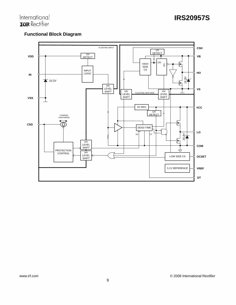
Description The IRS20957S is a high voltage, high speed MOSFET driver with a floating PWM input designed for Class D audio amplifier applications. Bi-directional current sensing detects over current conditions during positive and negative load currents without any external shunt resistors. A built-in protection control block provides a secure protection sequence against over-current conditions and a programmable reset timer. The internal dead-time generation block enables accurate gate switching and optimum dead-time setting for better audio performance, such as lower THD and lower audio noise floor.

IRS20957S
www.irf.com © 2008 International Rectifier
4
Qualification Information†
Qualification Level
Industrial††
Comments: This family of ICs has passed JEDEC’s Industrial qualification. IR’s Consumer qualification level is granted by extension of the higher Industrial level.
Moisture Sensitivity Level SOIC16N MSL2
†††260°C
(per IPC/JEDEC J-STD-020)
ESD Machine Model
Class B (per JEDEC standard EIA/JESD22-A115)
Human Body Model Class 2
(per EIA/JEDEC standard JESD22-A114)
IC Latch-Up Test Class I , Level A
(per JESD78)
RoHS Compliant Yes
† Qualification standards can be found at International Rectifier’s web site http://www.irf.com/ †† Higher qualification ratings may be available should the user have such requirements. Please
contact your International Rectifier sales representative for further information. ††† Higher MSL ratings may be available for the specific package types listed here. Please contact
your International Rectifier sales representative for further information.

IRS20957S
www.irf.com © 2008 International Rectifier
5
Absolute Maximum Ratings Absolute Maximum Ratings indicate sustained limits beyond which damage to the device may occur. All voltage parameters are absolute voltages referenced to COM; all currents are defined positive into any lead. The Thermal Resistance and Power Dissipation ratings are measured under board mounted and still air conditions.
Symbol Definition Min. Max. Units
VB High side floating supply voltage -0.3 215
V
VS High side floating supply voltage† VB-15 VB+0.3
VHO High side floating output voltage Vs-0.3 VB+0.3
VCSH CSH pin input voltage Vs-0.3 VB+0.3
VCC Low side fixed supply voltage† -0.3 20
VLO Low side output voltage -0.3 VCC +0.3
VDD Floating input supply voltage -0.3 210
VSS Floating input supply voltage† (See IDDZ) VDD+0.3
VIN PWM input voltage VSS -0.3 VDD+0.3
VCSD CSD pin input voltage VSS -0.3 VDD+0.3
VDT DT pin input voltage -0.3 VCC +0.3
VOCSET OCSET pin input voltage -0.3 VCC +0.3
VREF VREF pin voltage -0.3 VCC +0.3
IDDZ Floating input supply zener clamp current† - 10
mA ICCZ Low side supply zener clamp current
† - 10
IBSZ Floating supply zener clamp current† - 10
IOREF Reference output current - 5
d VS /dt Allowable VS voltage slew rate - 50 V/ns
d VSS /dt Allowable VSS voltage slew rate††
- 50
d VSS /dt Allowable VSS voltage slew rate upon power-up†††
- 50 V/ms
Pd Maximum power dissipation - 1.0 W
RthJA Thermal resistance, Junction to ambient - 115 C/W
TJ Junction Temperature - 150
C TS Storage Temperature -55 150
TL Lead temperature (Soldering, 10 seconds) - 300
† VDD - VSS, VCC -COM and VB - VS contain internal shunt zener diodes. Please note that the
voltage ratings of these can be limited by the clamping current. †† For the rising and falling edges of step signal of 10V. Vss=15V to 200V. ††† Vss ramps up from 0V to 200V.

IRS20957S
www.irf.com © 2008 International Rectifier
6
Recommended Operating Conditions For proper operation, the device should be used within the recommended conditions below. The Vs and COM offset ratings are tested with supplies biased at IDD=5mA, VCC=12V and VB-VS=12V.
Symbol Definition Min. Max. Units
VB High side floating supply absolute voltage Vs+10 Vs+14 V
VS High side floating supply offset voltage † 200
IDDZ Floating input supply zener clamp current 1 5 mA
VSS Floating input supply absolute voltage 0 100
V
VHO High side floating output voltage Vs VB
VCC Low side fixed supply voltage 10 15
VLO Low side output voltage 0 VCC
VIN PWM input voltage VSS VDD
VCSD CSD pin input voltage VSS VDD
VDT DT pin input voltage 0 VCC
IOREF Reference output current to COM† 0.3 0.8 mA
VOCSET OCSET pin input voltage 0.5 5 V
TA Ambient Temperature -40 125 C
† Logic operational for Vs equal to –5V to +200V. Logic state held for Vs equal to –5V to –VBS. †† Nominal voltage for VREF is 5V. IOREF of 0.3 – 0.8mA dictates total external resistor value on
VREF to be 6.3k to 16.7k Ω.

IRS20957S
www.irf.com © 2008 International Rectifier
7
Electrical Characteristics VCC,VBS= 12 V, IDD=5mA, VSS=20V, VS=0V,CL=1nF and TA=25C unless otherwise specified.
Symbol Description Min Typ Max Units Test Conditions
Low Side Supply
UVCC+ VCC supply UVLO positive threshold
8.4 8.9 9.4
V
UVCC- VCC supply UVLO negative threshold
8.2 8.7 9.2
IQCC Low side quiescent current - - 3 mA VDT = VCC
VCLAMPL Low side zener diode clamp voltage
19.6 20.4 21.6 V ICC=5mA
High Side Floating Supply
UVBS+ High side well UVLO positive threshold
8.0 8.5 9.0 V
UVBS- High side well UVLO negative threshold
7.8 8.3 8.8
IQBS High side quiescent current - - 1 mA
ILKH High to Low side leakage current
- - 50 µA VB=VS =200V
VCLAMPH High side zener diode clamp voltage
14.7 15.3 16.2 V IBS=5mA
Floating Input Supply
UVDD+ VDD, VSS floating supply UVLO positive threshold
8.2 8.7 9.2
V
VSS =0V
UVDD- VDD, VSS floating supply UVLO negative threshold
7.7 8.2 8.7 VSS =0V
IQDD Floating Input quiescent current
- - 1 mA VDD=9.5V +Vss
VCLAMPM Floating Input zener diode clamp voltage
9.8 10.2 10.8 V IDD=5mA
ILKM Floating input side to Low side leakage current
- - 50 µA VDD=VSS =200V
Floating PWM Input
VIH Logic high input threshold voltage
2.3 1.9 -
V
VIL Logic low input threshold voltage
- 1.9 1.5
IIN+ Logic “1” input bias current - - 40 µA
VIN =3.3V
IIN- Logic “0” input bias current - - 1 VIN = VSS
Protection
VREF Reference output voltage 4.8 5.1 5.4
V
IOREF =0.5mA
VthOCL Low side OC threshold in Vs
1.1 1.2 1.3 OCSET=1.2V,
Figure 3
VthOCH High side OC threshold in VCSH
1.1+ Vs 1.2+ Vs 1.3+ Vs Vs=200V, Figure 4
Vth1 CSD pin shutdown release threshold
0.62xVDD 0.70xVDD 0.78xVDD VSS =0V
Vth2 CSD pin self reset threshold 0.26xVDD 0.30xVDD 0.34xVDD VSS =0V
ICSD+ CSD pin discharge current 70 100 130 µA
VSD = VSS +5V
ICSD- CSD pin charge current 70 100 130 VSD = VSS +5V
IRS20957S
www.irf.com © 2008 International Rectifier
8
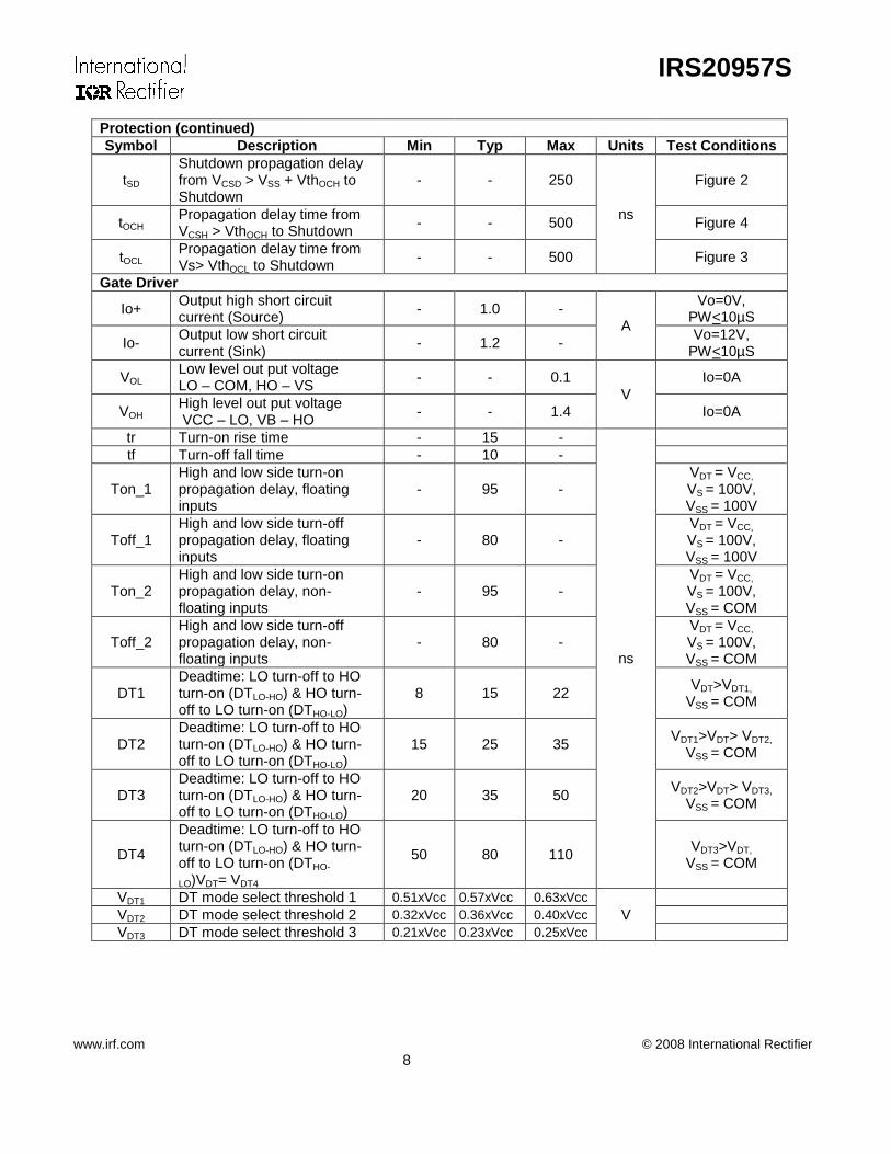
Protection (continued)
Symbol Description Min Typ Max Units Test Conditions
tSD Shutdown propagation delay from VCSD > VSS + VthOCH to Shutdown
- - 250
ns
Figure 2
tOCH Propagation delay time from VCSH > VthOCH to Shutdown
- - 500 Figure 4
tOCL Propagation delay time from Vs> VthOCL to Shutdown
- - 500 Figure 3
Gate Driver
Io+ Output high short circuit current (Source)
- 1.0 - A
Vo=0V, PW<10µS
Io- Output low short circuit current (Sink)
- 1.2 - Vo=12V,
PW<10µS
VOL Low level out put voltage LO – COM, HO – VS
- - 0.1
V
Io=0A
VOH High level out put voltage VCC – LO, VB – HO
- - 1.4 Io=0A
tr Turn-on rise time - 15 -
ns
tf Turn-off fall time - 10 -
Ton_1 High and low side turn-on propagation delay, floating inputs
- 95 - VDT = VCC,
VS = 100V, VSS = 100V
Toff_1 High and low side turn-off propagation delay, floating inputs
- 80 - VDT = VCC,
VS = 100V, VSS = 100V
Ton_2 High and low side turn-on propagation delay, non-floating inputs
- 95 - VDT = VCC,
VS = 100V, VSS = COM
Toff_2 High and low side turn-off propagation delay, non-floating inputs
- 80 - VDT = VCC,
VS = 100V, VSS = COM
DT1 Deadtime: LO turn-off to HO turn-on (DTLO-HO) & HO turn-off to LO turn-on (DTHO-LO)
8 15 22 VDT>VDT1,
VSS = COM
DT2 Deadtime: LO turn-off to HO turn-on (DTLO-HO) & HO turn-off to LO turn-on (DTHO-LO)
15 25 35 VDT1>VDT> VDT2,
VSS = COM
DT3 Deadtime: LO turn-off to HO turn-on (DTLO-HO) & HO turn-off to LO turn-on (DTHO-LO)
20 35 50 VDT2>VDT> VDT3,
VSS = COM
DT4
Deadtime: LO turn-off to HO turn-on (DTLO-HO) & HO turn-off to LO turn-on (DTHO-
LO)VDT= VDT4
50 80 110 VDT3>VDT,
VSS = COM
VDT1 DT mode select threshold 1 0.51xVcc 0.57xVcc 0.63xVcc
V
VDT2 DT mode select threshold 2 0.32xVcc 0.36xVcc 0.40xVcc
VDT3 DT mode select threshold 3 0.21xVcc 0.23xVcc 0.25xVcc
IRS20957S
www.irf.com © 2008 International Rectifier
9
Functional Block Diagram
HIGH
SIDE
CS
VB
HO
VS
IN
LOW SIDE CS
CSD
UV
Q
UV
DETECT
DEAD-TIME
VCC
LO
COM
VDD
VSS
CSH
PROTECTION
CONTROL
SD
OCSET
UV
DETECTUV
DETECT
CHARGE/
DISCHARGE
HV
LEVEL
SHIFT
HV
LEVEL
SHIFT
HV
LEVEL
SHIFT
FLOATING INPUT
FLOATING HIGH SIDE
HV
LEVEL
SHIFT
HV
LEVEL
SHIFT
5V REG
DT
DT
INPUT
LOGIC
10.2V
15
.3V
20
.4V
VREF5.1V REFERENCE

IRS20957S
www.irf.com © 2008 International Rectifier
10
I/O Pin Equivalent Circuit Diagrams
ESD Diode
ESD Diode
VDD
CSD
VSS
10V
Clamp
VSS
215 V
ESD Diode
ESD Diode
VB
HO
VS
ESD Diode
ESD Diode
LO
COM
215 V
15 V Clamp
20 V Clamp
V CC
VCC
ESD Diode
ESD Diode
VCC
DT, VREFor
OCSET
COM
ESD Diode
ESD Diode
VB
CSH
VS
IRS20957S
www.irf.com © 2008 International Rectifier
11
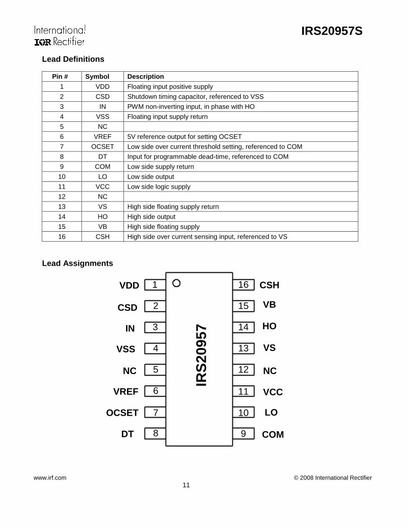
Lead Definitions
Pin # Symbol Description
1 VDD Floating input positive supply
2 CSD Shutdown timing capacitor, referenced to VSS
3 IN PWM non-inverting input, in phase with HO
4 VSS Floating input supply return
5 NC
6 VREF 5V reference output for setting OCSET
7 OCSET Low side over current threshold setting, referenced to COM
8 DT Input for programmable dead-time, referenced to COM
9 COM Low side supply return
10 LO Low side output
11 VCC Low side logic supply
12 NC
13 VS High side floating supply return
14 HO High side output
15 VB High side floating supply
16 CSH High side over current sensing input, referenced to VS
Lead Assignments
1
2
3
4
5
6
7
8
16
15
14
13
12
11
10
9
IRS
209
57
VDD
IN
CSD
VSS
OCSET
DT
VREF
COM
LO
VCC
HO
VS
CSH
VB
NC NC

IRS20957S
www.irf.com © 2008 International Rectifier
12
Waveform definitions
50% 50%
toff(L)
ton(L)
90%
10%
90%
10%
DTLO-HO
toff(H)
COMP
LO
HO
ton(H)
DTHO-LO
Vth1
tSD
90%
CSD
HO/LO
Figure 1: Switching Time Waveform Definitions Figure 2: CSD to Shutdown Waveform Definitions
VthOCL
tOCL
90%
VS
LO
VthOCH
tOCH
90%
CSH
HO
VS
Figure 3: VS > VthOCL to Shutdown Waveform Figure 4: VCSH > VthOCH to Shutdown Waveform
Application information and additional information Please refer to AN-1144 for IRS20957 functional description.

IRS20957S
www.irf.com © 2008 International Rectifier
13
Package Details: SOIC16N

IRS20957S
www.irf.com © 2008 International Rectifier
14
Package Details: SOIC16N, Tape and Reel
CARRIER TAPE DIMENSION FOR 16SOICN
Code Min Max Min Max
A 7.90 8.10 0.311 0.318
B 3.90 4.10 0.153 0.161
C 15.70 16.30 0.618 0.641
D 7.40 7.60 0.291 0.299
E 6.40 6.60 0.252 0.260
F 10.20 10.40 0.402 0.409
G 1.50 n/a 0.059 n/a
H 1.50 1.60 0.059 0.062
Metric Imperial
REEL DIMENSIONS FOR 16SOICN
Code Min Max Min Max
A 329.60 330.25 12.976 13.001
B 20.95 21.45 0.824 0.844
C 12.80 13.20 0.503 0.519
D 1.95 2.45 0.767 0.096
E 98.00 102.00 3.858 4.015
F n/a 22.40 n/a 0.881
G 18.50 21.10 0.728 0.830
H 16.40 18.40 0.645 0.724
Metric Imperial
E
F
A
C
D
G
AB H
NOTE : CONTROLLING
DIMENSION IN MM
LOADED TAPE FEED DIRECTION
A
H
F
E
G
D
BC

IRS20957S
www.irf.com © 2008 International Rectifier
15
Part Marking Information
IRSxxxxx
IR logo YWW ?
Part number
Date code
Pin 1
Identifier
Lot Code
(Prod mode –
4 digit SPN code)
Assembly site code
Per SCOP 200-002
? XXXX
MARKING CODE
Lead Free Released
Non-Lead Free Released
?
P

IRS20957S
www.irf.com © 2008 International Rectifier
16
Ordering Information
Base Part Number Package Type Standard Pack
Complete Part Number Form Quantity
IRS20957S SOIC16N Tube/Bulk 45 IRS20957SPBF
Tape and Reel 2500 IRS20957STRPBF
The information provided in this document is believed to be accurate and reliable. However, International Rectifier assumes no
responsibility for the consequences of the use of this information. International Rectifier assumes no responsibility for any infringement of patents or of other rights of third parties which may result from the use of this information. No license is granted by implication or otherwise under any patent or patent rights of International Rectifier. The specifications mentioned in this document are subject to
change without notice. This document supersedes and replaces all information previously supplied.
For technical support, please contact IR’s Technical Assistance Center http://www.irf.com/technical-info/
WORLD HEADQUARTERS:
233 Kansas St., El Segundo, California 90245 Tel: (310) 252-7105

IRS20957S
www.irf.com © 2008 International Rectifier
17
Change History March 14, 2008 1) Updated the format 2) Added Product Summary 3) Added Qualification table
March 18, 2008 1) Added package details, part marking, ordering info
April 22, 2008 1) Inserted ton, toff typical numbers 2) Removed unnecessary place holders 3) Inserted I/O dwgs 4) Fixed formatting on tables 5) Changed copyright to 2008 instead of 2007 6) Added waveform definition section based on IRS20954/5 DS April 23, 2008 1) Changed topology to HBridge 2) Changed ton typical to 95ns (on product summary table and elec. Char. Table) April 24, 2008 1) Changed Typical Connection Diagram 2) Changed High side zener diode clamp voltage 3) Changed I/O Pin Equivalent Circuit Diagrams Absolute Maximum Ratings
VB High side floating supply voltage -0.3 215 V
VS High side floating supply voltage (Note1) VB-15 VB+0.3 V
Recommended Operating Conditions
VB High side floating supply absolute voltage Vs+10 Vs+14 V
VCC Low side fixed supply voltage 10 15 V
April 29, 2008 1) Changed format
2) Changed “note1, 2, 3” to “†, ††, †††” June 12, 08 1) Replaced part marking information with the latest version June 23, 08
1) Updated std pack quantity for SO16N to 45 pcs August 4
th, 2008:
1) added typical applications on page 1 2) removed PbF from product name on page 1 3) Merge units in table 4) Added “Application information and additional details” on page 12.

IRS20957S
www.irf.com © 2008 International Rectifier
18
September 10th, 2008
1) Added AN-1144 on page 12 March 5, 2009 Added PD number Sept 19, 2016 Corrected typos: “All voltage parameters are absolute voltages referenced to COM;”
ESD Diode
ESD Diode
VDD
CSD
VSS
10V
Clamp
VSS
215 V
ESD Diode
ESD Diode
VB
HO
VS
ESD Diode
ESD Diode
LO
COM
215 V
15 V Clamp
20 V Clamp
V CC
VCC