Embed Size (px)
Citation preview
PE42522Product SpecificationUltraCMOS® SPDT RF Switch, 9 kHz–26.5 GHz
Features• Broad frequency support from 9 kHz to 26.5 GHz• High port to port isolation
▪ 63 dB @ 3 GHz▪ 58 dB @ 7.5 GHz▪ 39 dB @ 13.5 GHz▪ 28 dB @ 20 GHz▪ 22 dB @ 26.5 GHz
• HaRP™ technology enhanced▪ Fast settling time▪ No gate and phase lag▪ No drift in insertion loss and phase
• Improved high frequency insertion loss and return loss performance with external matching
• High ESD performance of 3.5 kV HBM on all pins• Packaging – 29-lead 4 × 4 mm LGA
Applications• Test and measurement• Microwave backhaul• Radar
Product DescriptionThe PE42522 is a HaRP™ technology-enhanced absorptive SPDT RF switch that supports a broad frequency range from 9 kHz to 26.5 GHz. This broadband general purpose switch offers excellent isolation, high linearity performance and has exceptional settling time making this device ideal for many broadband wireless applica-tions. No blocking capacitors are required if DC voltage is not present on the RF ports.
The PE42522 is manufactured on Peregrine’s UltraCMOS® process, a patented variation of silicon-on-insulator (SOI) technology on a sapphire substrate.
Peregrine’s HaRP technology enhancements deliver high linearity and excellent harmonics performance. It is an innovative feature of the UltraCMOS process, offering the performance of GaAs with the economy and integration of conventional CMOS.
Figure 1 • PE42522 Functional Diagram
RFC
50Ω 50Ω
CMOS Control Driver
RF2RF1
V1 VSS_EXT
©2014-2015, Peregrine Semiconductor Corporation. All rights reserved. • Headquarters: 9380 Carroll Park Drive, San Diego, CA, 92121
Product Specification DOC-12014-6 – (2/2015)www.psemi.com
PE42522UltraCMOS® SPDT RF Switch
Optional External VSS Control For proper operation, the VSS_EXT control pin must be grounded or tied to the VSS voltage specified in Table 2. When the VSS_EXT control pin is grounded, FETs in the switch are biased with an internal negative voltage generator. For applications that require the lowest possible spur performance, VSS_EXT can be applied externally to bypass the internal negative voltage generator.
Absolute Maximum RatingsExceeding absolute maximum ratings listed in Table 1 may cause permanent damage. Operation should be restricted to the limits in Table 2. Operation between operating range maximum and absolute maximum for extended periods may reduce reliability.
ESD PrecautionsWhen handling this UltraCMOS device, observe the same precautions as with any other ESD-sensitive devices. Although this device contains circuitry to protect it from damage due to ESD, precautions should be taken to avoid exceeding the rating specified in Table 1.
Latch-up ImmunityUnlike conventional CMOS devices, UltraCMOS devices are immune to latch-up.
Table 1 • Absolute Maximum Ratings for PE42522
Parameter/Condition Min Max Unit
Supply voltage, VDD –0.3 5.5 V
Digital input voltage, V1 –0.3 3.6 V
RF input power, CW (RFC–RFX)(1)
9 kHz–2.89 MHz>2.89 MHz–18 GHz >18–26.5 GHz
Fig. 2, Fig. 333
Fig. 4
dBmdBmdBm
RF input power, pulsed (RFC–RFX)(2)
9 kHz–2.89 MHz>2.89 MHz–18 GHz >18–26.5 GHz
Fig. 2, Fig. 334
Fig. 4
dBmdBmdBm
RF input power into terminated ports, CW (RFX)(1)
9 kHz–1.39 MHz>1.39 MHz–18 GHz >18–26.5 GHz
Fig. 2, Fig. 322
Fig. 4
dBmdBmdBm
Storage temperature range –65 +150 °C
ESD voltage HBM, all pins(3) 3500 V
ESD voltage MM, all pins(4) 150 V
ESD voltage CDM, all pins(5) 500 V
Page 2 DOC-12014-6 – (2/2015)www.psemi.com
PE42522UltraCMOS® SPDT RF Switch
Recommended Operating ConditionsTable 2 list the recommending operating condition for PE42522. Devices should not be operated outside the recommended operating conditions listed below.
Notes: 1) 100% duty cycle, all bands, 50Ω.2) Pulsed, 5% duty cycle of 4620 μs period, 50Ω.3) Human body model (MIL-STD 883 Method 3015).4) Machine model (JEDEC JESD22-A115).5) Charged device model (JEDEC JESD22-C101).
Table 2 • Recommended Operating Condition for PE42522
Parameter Min Typ Max Unit
Normal mode (VSS_EXT = 0V)(1)
Supply voltage, VDD 2.3 5.5 V
Supply current, IDD 120 200 μA
Bypass mode (VSS_EXT = –3.4V)(2)
Supply voltage, VDD
(VDD ≥3.4V for Table 3 full spec. compliance)2.7 3.4 5.5 V
Supply current, IDD 50 80 μA
Negative supply voltage, VSS_EXT –3.6 –3.2 V
Negative supply current, ISS –40 –16 μA
Normal or Bypass mode
Digital input high, V1 1.17 3.6 V
Digital input low, V1 –0.3 0.6 V
RF input power, CW (RFC–RFX)(3)
9 kHz–2.89 MHz>2.89 MHz–18 GHz>18–26.5 GHz
Fig. 2, Fig. 330
Fig. 4
dBmdBmdBm
RF input power, pulsed (RFC–RFX)(4)
9 kHz–2.89 MHz>2.89 MHz–18 GHz>18–26.5 GHz
Fig. 2, Fig. 332
Fig. 4
dBmdBmdBm
Table 1 • Absolute Maximum Ratings for PE42522 (Cont.)
Parameter/Condition Min Max Unit
DOC-12014-6 – (2/2015) Page 3www.psemi.com

PE42522UltraCMOS® SPDT RF Switch
Electrical SpecificationsTable 3 provides the PE42522 key electrical specifications at 25 °C (ZS = ZL = 50Ω), unless otherwise specified. Normal mode(1) is at VDD = 3.3V and VSS_EXT = 0V. Bypass mode(2) is at VDD = 3.4V and VSS_EXT = –3.4V.
RF input power into terminated ports, CW (RFX)(3)
9 kHz–1.39 MHz>1.39 MHz–18 GHz>18–26.5 GHz
Fig. 2, Fig. 320
Fig. 4
dBmdBmdBm
Operating temperature range, TOP –40 +25 +85 °C
Notes: 1) Normal mode: connect VSS_EXT (pin 29) to GND (VSS_EXT = 0V) to enable internal negative voltage generator.
2) Bypass mode: use VSS_EXT (pin 29) to bypass and disable internal negative voltage generator.
3) 100% duty cycle, all bands, 50Ω.4) Pulsed, 5% duty cycle of 4620 μs period, 50Ω.
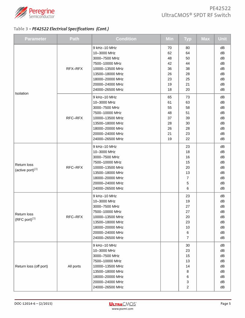
Table 3 • PE42522 Electrical Specifications
Parameter Path Condition Min Typ Max Unit
Operating frequency 9 kHz 26.5 GHz As shown
Insertion loss(3) RFC–RFX
9 kHz–10 MHz10–3000 MHz3000–7500 MHz7500–10000 MHz10000–13500 MHz13500–18000 MHz18000–20000 MHz20000–24000 MHz24000–26500 MHz
0.701.051.151.701.702.553.154.205.30
0.851.401.502.152.403.254.405.456.95
dBdBdBdBdBdBdBdBdB
Table 2 • Recommended Operating Condition for PE42522 (Cont.)
Parameter Min Typ Max Unit
Page 4 DOC-12014-6 – (2/2015)www.psemi.com
PE42522UltraCMOS® SPDT RF Switch
Isolation
RFX–RFX
9 kHz–10 MHz10–3000 MHz3000–7500 MHz7500–10000 MHz10000–13500 MHz13500–18000 MHz18000–20000 MHz20000–24000 MHz24000–26500 MHz
706248423626231918
806450443828252120
dBdBdBdBdBdBdBdBdB
RFC–RFX
9 kHz–10 MHz10–3000 MHz3000–7500 MHz7500–10000 MHz10000–13500 MHz13500–18000 MHz18000–20000 MHz20000–24000 MHz24000–26500 MHz
656155483728262119
736358513930282322
dBdBdBdBdBdBdBdBdB
Return loss (active port)(3) RFC–RFX
9 kHz–10 MHz10–3000 MHz3000–7500 MHz7500–10000 MHz10000–13500 MHz13500–18000 MHz18000–20000 MHz20000–24000 MHz24000–26500 MHz
231816152013756
dBdBdBdBdBdBdBdBdB
Return loss (RFC port)(3) RFC–RFX
9 kHz–10 MHz10–3000 MHz3000–7500 MHz7500–10000 MHz10000–13500 MHz13500–18000 MHz18000–20000 MHz20000–24000 MHz24000–26500 MHz
2319272720231067
dBdBdBdBdBdBdBdBdB
Return loss (off port) All ports
9 kHz–10 MHz10–3000 MHz3000–7500 MHz7500–10000 MHz10000–13500 MHz13500–18000 MHz18000–20000 MHz20000–24000 MHz24000–26500 MHz
30231513148632
dBdBdBdBdBdBdBdBdB
Table 3 • PE42522 Electrical Specifications (Cont.)
Parameter Path Condition Min Typ Max Unit
DOC-12014-6 – (2/2015) Page 5www.psemi.com
PE42522UltraCMOS® SPDT RF Switch
Switching FrequencyThe PE42522 has a maximum 25 kHz switching rate in normal mode (pin 29 tied to ground). A faster switching rate is available in bypass mode (pin 29 tied to VSS_EXT). The rate at which the PE42522 can be switched is then limited to the switching time as specified in Table 3.
Switching frequency describes the time duration between switching events. Switching time is the time duration between the point the control signal reached 50% of the final value and the point the output signal reaches within 10% or 90% of its target value.
Spur-Free PerformanceThe typical spurious performance of the PE42522 in normal mode is –125 dBm (pin 29 tied to ground). If spur-free performance is desired, the internal negative voltage generator can be disabled by applying a negative voltage to VSS_EXT (pin 29).
Hot-Switching CapabilityThe maximum hot switching capability of the PE42522 is 20 dBm from 1.4 MHz to 18 GHz. The maximum hot switching capability below 1.4 MHz and above 18 GHz does not exceed the maximum RF CW terminated power, see Figure 2–Figure 4. Hot switching occurs when RF power is applied while switching between RF ports.
Control LogicTable 4 provides the control logic truth table for PE42522.
Input 0.1dB compression point(4) RFC–RFX
Fig. 2Fig. 3Fig. 4
dBmdBmdBm
Input IP2 RFC–RFX 10–18000 MHz 121 dBm
Input IP3 RFC–RFX 10–18000 MHz 59 dBm
Settling time 50% CTRL to 0.05 dB final value 7 10 μs
Switching time 50% CTRL to 90% or 10% of RF 3 4.5 μs
Notes: 1) Normal mode: connect VSS_EXT (pin 29) to GND (VSS_EXT = 0V) to enable internal negative voltage generator.
2) Bypass mode: use VSS_EXT (pin 29) to bypass and disable internal negative voltage generator.
3) High frequency performance can be improved by external matching (see Figure 19–Figure 21).4) The input 0.1dB compression point is a linearity figure of merit. Refer to Table 2 for the RF input power (50Ω).
Table 3 • PE42522 Electrical Specifications (Cont.)
Parameter Path Condition Min Typ Max Unit
Table 4 • Truth Table for PE42522
State V1
RF1 ON 0
RF2 ON 1
Page 6 DOC-12014-6 – (2/2015)www.psemi.com
PE42522UltraCMOS® SPDT RF Switch
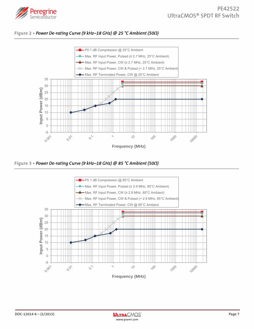
Figure 2 • Power De-rating Curve (9 kHz–18 GHz) @ 25 °C Ambient (50Ω)
-5
0
5
10
15
20
25
30
35
Inpu
t Pow
er (d
Bm
)
Frequency (MHz)
P0.1 dB Compression @ 25°C Ambient
Max. RF Input Power, Pulsed (≥ 2.7 MHz, 25°C Ambient)
Max. RF Input Power, CW (≥ 2.7 MHz, 25°C Ambient)
Max. RF Input Power, CW & Pulsed (< 2.7 MHz, 25°C Ambient)
Max. RF Terminated Power, CW @ 25°C Ambient
Figure 3 • Power De-rating Curve (9 kHz–18 GHz) @ 85 °C Ambient (50Ω)
-5
0
5
10
15
20
25
30
35
Inpu
t Pow
er (d
Bm
)
Frequency (MHz)
P0.1 dB Compression @ 85°C Ambient
Max. RF Input Power, Pulsed (≥ 2.9 MHz, 85°C Ambient)
Max. RF Input Power, CW (≥ 2.9 MHz, 85°C Ambient)
Max. RF Input Power, CW & Pulsed (< 2.9 MHz, 85°C Ambient)
Max. RF Terminated Power, CW @ 85°C Ambient
DOC-12014-6 – (2/2015) Page 7www.psemi.com

PE42522UltraCMOS® SPDT RF Switch
Figure 4 • Power De-rating Curve (16–26.5 GHz) @ 25 °C and 85 °C Ambient (50Ω)
14
16
18
20
22
24
26
28
30
32
34
36
16 18 20 22 24 26
Inpu
t Pow
er (d
Bm
)
Frequency (GHz)
Abs. Max. RF Input Power, Pulsed @ 25°C & 85°C Ambient
P0.1 dB Compression / Abs. Max. RF Input Power, CW @ 25°C & 85°C Ambient
Max. RF Input Power, Pulsed @ 25°C & 85°C Ambient
Max. RF Input Power, CW @ 25°C & 85°C Ambient
Abs. Max. RF Terminated Power @ 25°C & 85°C Ambient
Max. RF Terminated Power, CW @ 25°C & 85°C Ambient
Page 8 DOC-12014-6 – (2/2015)www.psemi.com
PE42522UltraCMOS® SPDT RF Switch
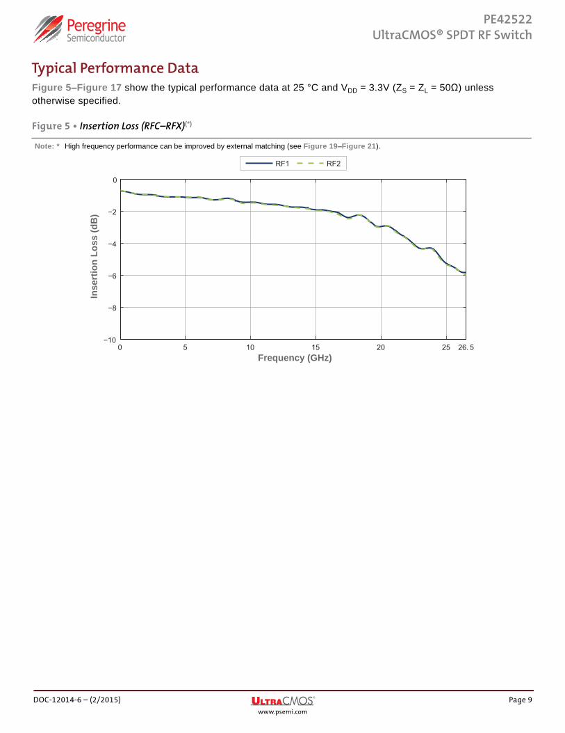
Typical Performance DataFigure 5–Figure 17 show the typical performance data at 25 °C and VDD = 3.3V (ZS = ZL = 50Ω) unless otherwise specified.
Figure 5 • Insertion Loss (RFC–RFX)(*)
Note: * High frequency performance can be improved by external matching (see Figure 19–Figure 21).
0 5 10 15 20 25 26. 5−10
−8
−6
−4
−2
0
Frequency (GHz)
Inse
rtio
n Lo
ss (d
B)
RF1 RF2
DOC-12014-6 – (2/2015) Page 9www.psemi.com

PE42522UltraCMOS® SPDT RF Switch
Figure 6 • Insertion Loss vs Temperature (RFC–RFX)(*)
Note: * High frequency performance can be improved by external matching (see Figure 19–Figure 21).
0 5 10 15 20 25 26. 5−10
−8
−6
−4
−2
0
Inse
rtio
n Lo
ss (d
B)
Frequency (GHz)
–40°C +25°C +85°C
Figure 7 • Insertion Loss vs VDD (RFC–RFX)(*)
Note: * High frequency performance can be improved by external matching (see Figure 19–Figure 21).
0 5 10 15 20 25 26. 5−10
−8
−6
−4
−2
0
Inse
rtio
n Lo
ss (d
B)
Frequency (GHz)
2.3V 3.3V 5.5V
Page 10 DOC-12014-6 – (2/2015)www.psemi.com
PE42522UltraCMOS® SPDT RF Switch
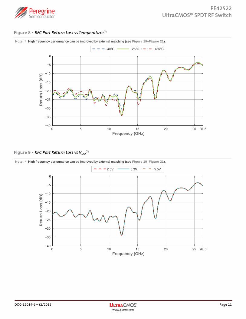
Figure 8 • RFC Port Return Loss vs Temperature(*)
Note: * High frequency performance can be improved by external matching (see Figure 19–Figure 21).
0 5 10 15 20 25 26. 5−40
−35
−30
−25
−20
−15
−10
−5
0
Ret
urn
Loss
(dB
)
Frequency (GHz)
–40°C +25°C +85°C
Figure 9 • RFC Port Return Loss vs VDD(*)
Note: * High frequency performance can be improved by external matching (see Figure 19–Figure 21).
0 5 10 15 20 25 26. 5−40
−35
−30
−25
−20
−15
−10
−5
0
Ret
urn
Loss
(dB
)
Frequency (GHz)
2.3V 3.3V 5.5V
DOC-12014-6 – (2/2015) Page 11www.psemi.com
PE42522UltraCMOS® SPDT RF Switch
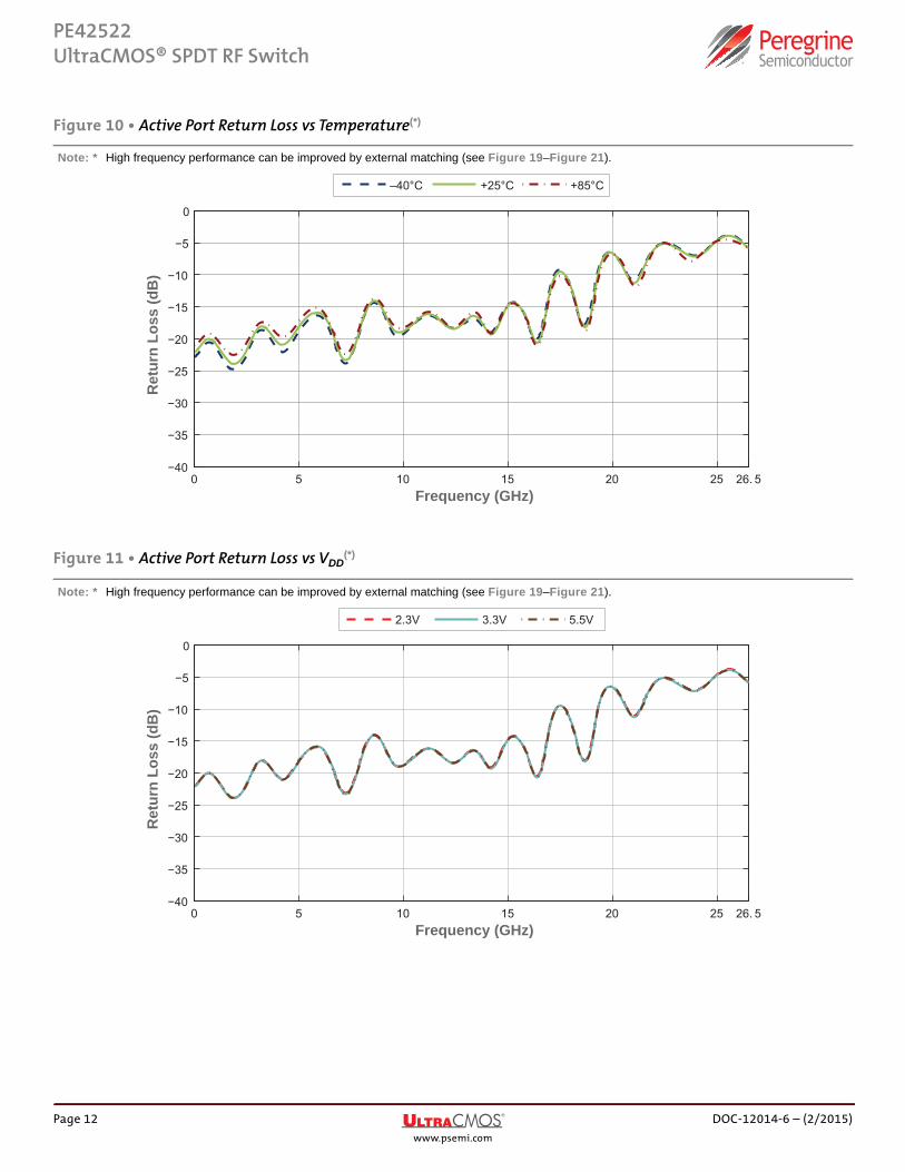
Figure 10 • Active Port Return Loss vs Temperature(*)
Note: * High frequency performance can be improved by external matching (see Figure 19–Figure 21).
0 5 10 15 20 25 26. 5−40
−35
−30
−25
−20
−15
−10
−5
0
Ret
urn
Loss
(dB
)
Frequency (GHz)
–40°C +25°C +85°C
Figure 11 • Active Port Return Loss vs VDD(*)
Note: * High frequency performance can be improved by external matching (see Figure 19–Figure 21).
0 5 10 15 20 25 26. 5−40
−35
−30
−25
−20
−15
−10
−5
0
Ret
urn
Loss
(dB
)
Frequency (GHz)
2.3V 3.3V 5.5V
Page 12 DOC-12014-6 – (2/2015)www.psemi.com

PE42522UltraCMOS® SPDT RF Switch
Figure 12 • Terminated Port Return Loss vs Temperature
0 5 10 15 20 25 26. 5−40
−35
−30
−25
−20
−15
−10
−5
0
Ret
urn
Loss
(dB
)
Frequency (GHz)
–40°C +25°C +85°C
Figure 13 • Terminated Port Return Loss vs VDD
0 5 10 15 20 25 26. 5−40
−35
−30
−25
−20
−15
−10
−5
0
Ret
urn
Loss
(dB
)
Frequency (GHz)
2.3V 3.3V 5.5V
DOC-12014-6 – (2/2015) Page 13www.psemi.com
PE42522UltraCMOS® SPDT RF Switch
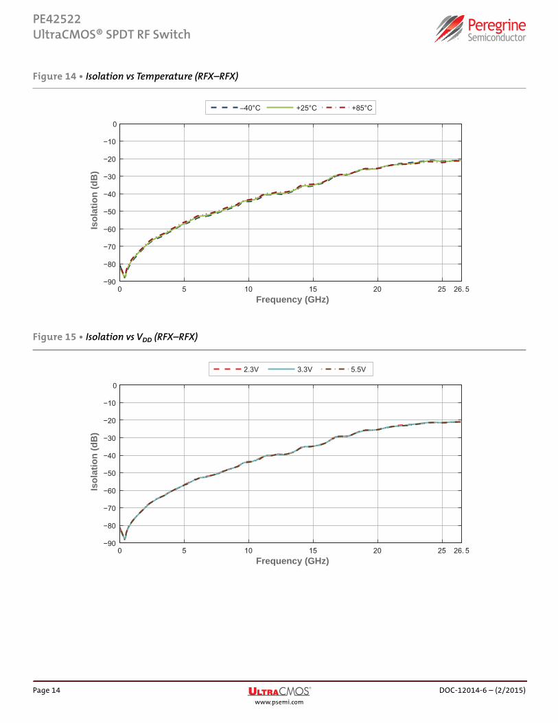
Figure 14 • Isolation vs Temperature (RFX–RFX)
0 5 10 15 20 25 26. 5−90
−80
−70
−60
−50
−40
−30
−20
−10
0
Frequency (GHz)
Isol
atio
n (d
B)
–40°C +25°C +85°C
Figure 15 • Isolation vs VDD (RFX–RFX)
0 5 10 15 20 25 26. 5−90
−80
−70
−60
−50
−40
−30
−20
−10
0
Frequency (GHz)
Isol
atio
n (d
B)
2.3V 3.3V 5.5V
Page 14 DOC-12014-6 – (2/2015)www.psemi.com
PE42522UltraCMOS® SPDT RF Switch
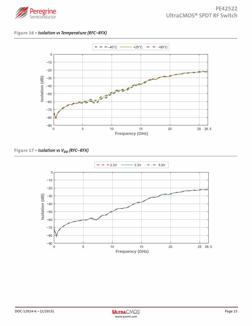
Figure 16 • Isolation vs Temperature (RFC–RFX)
0 5 10 15 20 25 26. 5−90
−80
−70
−60
−50
−40
−30
−20
−10
0
Frequency (GHz)
Isol
atio
n (d
B)
–40°C +25°C +85°C
Figure 17 • Isolation vs VDD (RFC–RFX)
0 5 10 15 20 25 26. 5−90
−80
−70
−60
−50
−40
−30
−20
−10
0
Frequency (GHz)
Isol
atio
n (d
B)
2.3V 3.3V 5.5V
DOC-12014-6 – (2/2015) Page 15www.psemi.com

PE42522UltraCMOS® SPDT RF Switch
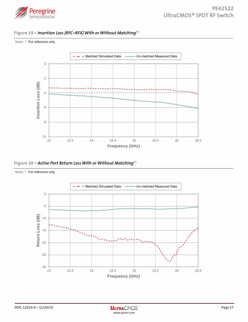
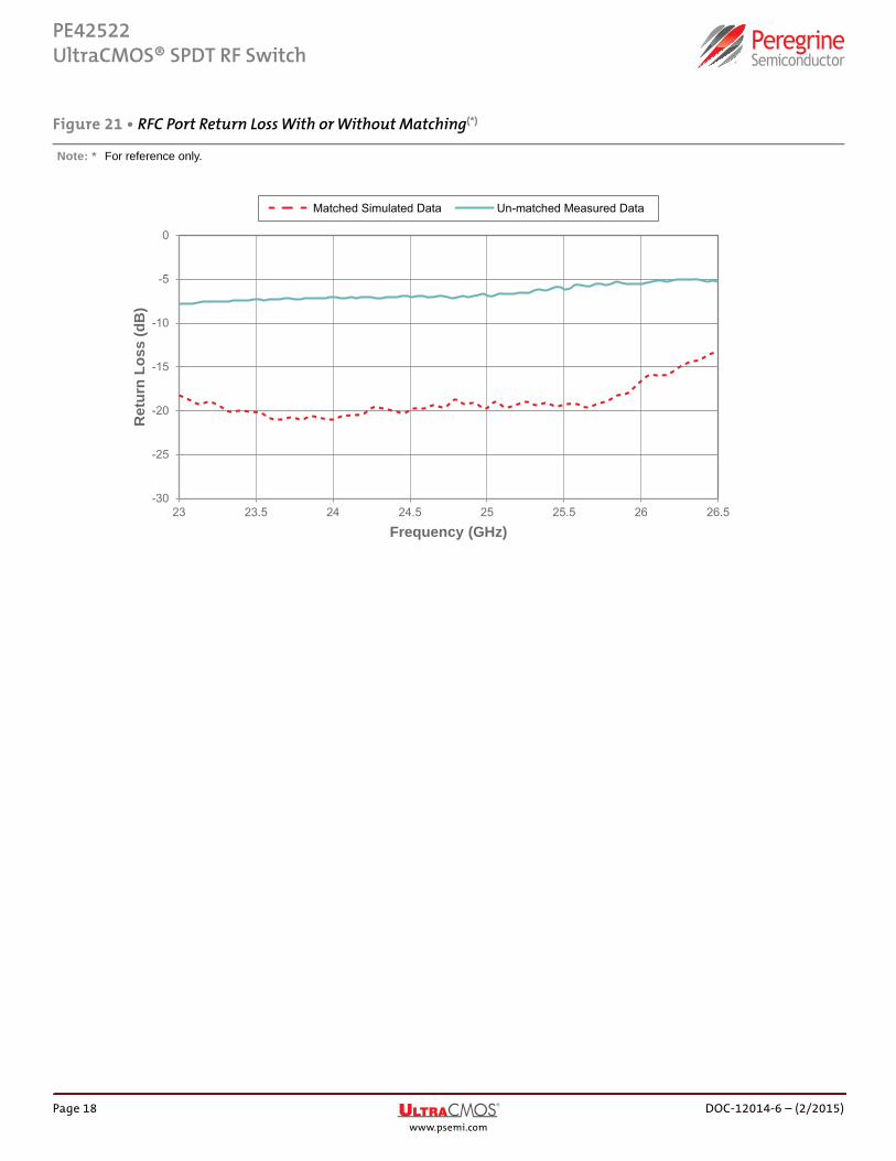
High Frequency Performance with External MatchingHigh frequency insertion loss and return loss can be further improved by external tuning traces in the customer application board layout. Figure 18 is a sample matching network using ideal elements. Figure 19–Figure 21 show the simulated insertion loss and return loss improvement using the matching network.
Additional information on high frequency performance with external matching can be found in Application Note 41, PE42522/523–High Frequency Performance Improvement Through Narrowband Matching.
Figure 18 • PE42522 Matching Network
SPDTPE42522
RF1
RFC
C1ANT = 200 fF
Matching can be realized with printed elements on the customer application board.
C1 = 175 fF C1 = 175 fF
L1ANT = 0.225 nH
L1 = 0.285 nHL2 = 0.300 nH L2 = 0.300 nHL1 = 0.285 nH
L2ANT = 0.200 nH
RF2
Page 16 DOC-12014-6 – (2/2015)www.psemi.com
PE42522UltraCMOS® SPDT RF Switch
Figure 19 • Insertion Loss (RFC–RFX) With or Without Matching(*)
Note: * For reference only.
-10
-8
-6
-4
-2
0
23 23.5 24 24.5 25 25.5 26 26.5
Inse
rtio
n Lo
ss (d
B)
Frequency (GHz)
Un-matched Measured DataMatched Simulated Data
Figure 20 • Active Port Return Loss With or Without Matching(*)
Note: * For reference only.
-30
-25
-20
-15
-10
-5
0
23 23.5 24 24.5 25 25.5 26 26.5
Ret
urn
Loss
(dB
)
Frequency (GHz)
Un-matched Measured DataMatched Simulated Data
DOC-12014-6 – (2/2015) Page 17www.psemi.com
PE42522UltraCMOS® SPDT RF Switch
Figure 21 • RFC Port Return Loss With or Without Matching(*)
Note: * For reference only.
-30
-25
-20
-15
-10
-5
0
23 23.5 24 24.5 25 25.5 26 26.5
Ret
urn
Loss
(dB
)
Frequency (GHz)
Un-matched Measured DataMatched Simulated Data
Page 18 DOC-12014-6 – (2/2015)www.psemi.com

PE42522UltraCMOS® SPDT RF Switch
Evaluation Kit The SPDT switch evaluation board was designed to ease customer evaluation of Peregrine's PE42522. The RF common port is connected through a 50Ω transmission line via the SMA connector, J1. RF1 and RF2 ports are connected through 50Ω transmission lines via SMA connectors J4 and J3 respectively. A 50Ω through trans-mission line is available via SMA connectors J6 and J7, which can be used to de-embed the loss of the PCB. J13 provides DC and digital inputs to the device.
The board is constructed of a two metal layer material with a total thickness of 38 mils. The top RF layer is Rogers 4360 material with a thickness of 32 mils and the εr = 6.4. The bottom layer provides ground for the transmission lines. The transmission lines were designed using a coplanar waveguide with ground plane model using a trace width of 18 mils, trace gaps of 7 mils and metal thickness of 2.1 mils.
For the true performance of the PE42522 to be realized, the PCB must be designed in such a way that RF trans-mission lines and sensitive DC I/O traces are well isolated from one another. High frequency insertion loss and return loss can be further improved by external tuning traces in the customer application board layout. For further details, see “High Frequency Performance with External Matching”.
Please note that this is a generic PCB and is being used for multiple parts. Pin labeled V2 is GND.
Figure 22 • Evaluation Kit Layout for PE42522
DOC-12014-6 – (2/2015) Page 19www.psemi.com
PE42522UltraCMOS® SPDT RF Switch
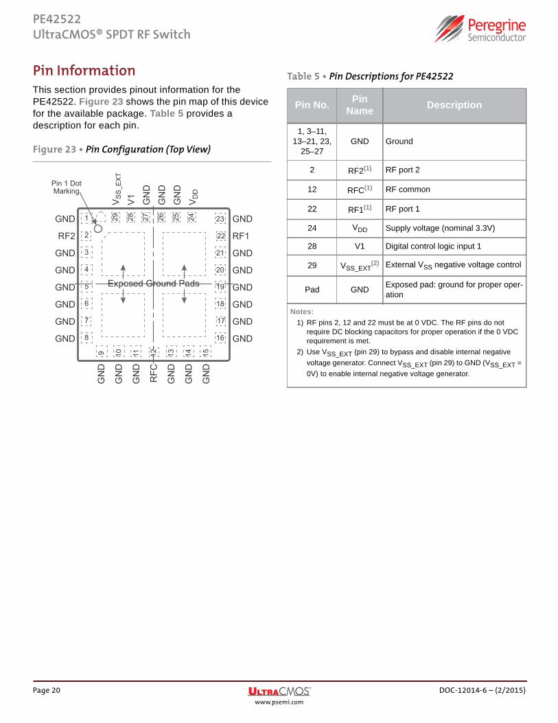
Pin InformationThis section provides pinout information for the PE42522. Figure 23 shows the pin map of this device for the available package. Table 5 provides a description for each pin.
Figure 23 • Pin Configuration (Top View)
Exposed Ground Pads
GND
RF1
GN
D
VD
D
GN
DG
ND
RFC
GN
D
GN
D
GN
D
V1
VS
S_E
XT
GN
D
GN
D
GN
D
GND
GND
GND
GND
GND
GND
GND
RF2
GND
GND
GND
GND
GND
GND
1
3
4
5
6
7
8
2
9 11 12 13 14 15
16
1029 28 27 26 25 24
22
21
20
19
18
17
23
Pin 1 DotMarking
Table 5 • Pin Descriptions for PE42522
Pin No. Pin Name Description
1, 3–11, 13–21, 23,
25–27GND Ground
2 RF2(1) RF port 2
12 RFC(1) RF common
22 RF1(1) RF port 1
24 VDD Supply voltage (nominal 3.3V)
28 V1 Digital control logic input 1
29 VSS_EXT(2) External VSS negative voltage control
Pad GND Exposed pad: ground for proper oper-ation
Notes: 1) RF pins 2, 12 and 22 must be at 0 VDC. The RF pins do not
require DC blocking capacitors for proper operation if the 0 VDC requirement is met.
2) Use VSS_EXT (pin 29) to bypass and disable internal negative voltage generator. Connect VSS_EXT (pin 29) to GND (VSS_EXT = 0V) to enable internal negative voltage generator.
Use VSS_EXT (pin 29) to bypass and disable internal negative voltage generator. Connect VSS_EXT (pin 29) to GND (VSS_EXT = 0V) to enable internal negative voltage generator.
Page 20 DOC-12014-6 – (2/2015)www.psemi.com

PE42522UltraCMOS® SPDT RF Switch
Packaging InformationThis section provides packaging data including the moisture sensitivity level, package drawing, package marking and tape-and-reel information.
Moisture Sensitivity LevelThe moisture sensitivity level rating for the PE42522 in the 29-lead 4 × 4 mm LGA package is MSL3.
DOC-12014-6 – (2/2015) Page 21www.psemi.com

PE42522UltraCMOS® SPDT RF Switch
Package Drawing Top-Marking Specification
Figure 24 • Package Mechanical Drawing for 29-lead 4 × 4 × 0.91 mm LGA
TOP VIEWBOTTOM VIEW
SIDE VIEW
RECOMMENDED LAND PATTERN
A (2X)
C
SEATING PLANE
B
(2X)
PIN #1 CORNER 4.00
4.00
1.13(x4)
1.13(x4)
0.46
0.490.10(x29)
0.70±0.05
0.20 x45°Chamfer
1.13 1.13
0.26x0.30(x6)
0.33x0.34(x18)
0.30x0.30(x5)
0.40
3.80
3.80
0.24(x4)
0.24(x4)
0.47
Note:- Dimensions concerning Pad pitch are allmirrored across the Y-axis
0.91±0.10
0.47
0.43
0.45
0.24(x4)
0.24(x4)
0.43
0.47
0.470.45
0.45
0.45
Pin Number Pin Size (x,y) X Coordinate Y Coordinate1 (0.285x0.280) 1.7575 1.74342 (0.250x0.250) 1.7750 1.27503 (0.285x0.280) 1.7575 0.84664 (0.285x0.280) 1.7575 0.39825 (0.285x0.280) 1.7575 -0.05026 (0.285x0.280) 1.7575 -0.49867 (0.250x0.250) 1.7750 -0.96708 (0.285x0.280) 1.7575 -1.39549 (0.280x0.285) 1.3652 -1.7575
10 (0.280x0.285) 0.9168 -1.757511 (0.280x0.285) 0.4684 -1.757512 (0.250x0.250) 0 -1.775013 (0.280x0.285) -0.4684 -1.757514 (0.280x0.285) -0.9168 -1.757515 (0.280x0.285) -1.3652 -1.757516 (0.285x0.280) -1.7575 -1.395417 (0.250x0.250) -1.7750 -0.967018 (0.285x0.280) -1.7575 -0.498619 (0.285x0.280) -1.7575 -0.050220 (0.285x0.280) -1.7575 0.398221 (0.285x0.280) -1.7575 0.846622 (0.250x0.250) -1.7750 1.275023 (0.285x0.280) -1.7575 1.743424 (0.210x0.250) -1 1.775025 (0.210x0.250) -0.600 1.775026 (0.210x0.250) -0.200 1.775027 (0.210x0.250) 0.200 1.775028 (0.210x0.250) 0.600 1.775029 (0.210x0.250) 1 1.7750
Page 22 DOC-12014-6 – (2/2015)www.psemi.com
PE42522UltraCMOS® SPDT RF Switch
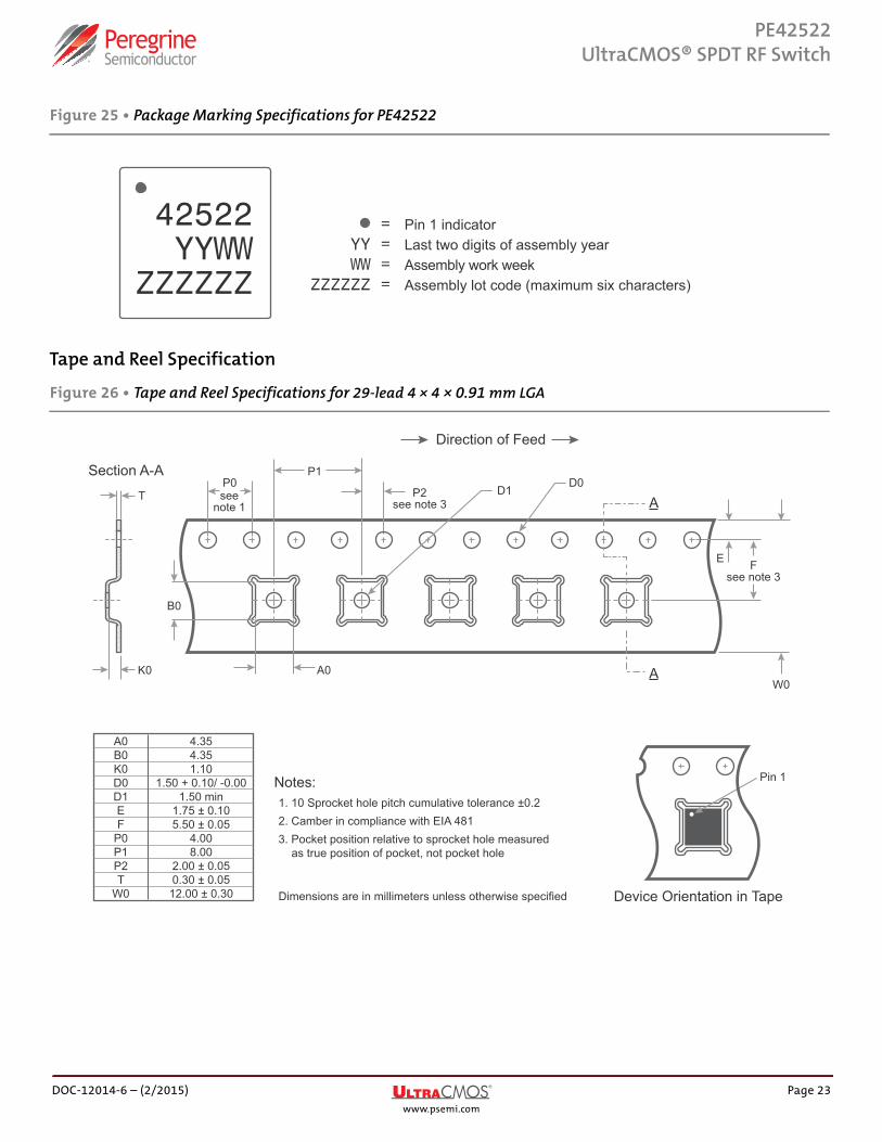
Tape and Reel Specification
Figure 25 • Package Marking Specifications for PE42522
Figure 26 • Tape and Reel Specifications for 29-lead 4 × 4 × 0.91 mm LGA
=YY =WW =
ZZZZZZ =
Pin 1 indicatorLast two digits of assembly yearAssembly work weekAssembly lot code (maximum six characters)
42522YYWW
ZZZZZZ
Device Orientation in Tape
Pin 1
T
K0 A0
B0
P0P1
D1A
Section A-A
A
Direction of Feed
D0
E
W0
P2see note 3
seenote 1
Fsee note 3
A0B0K0D0D1EF
P0P1P2T
W0
4.354.351.10
1.50 + 0.10/ -0.001.50 min
1.75 ± 0.105.50 ± 0.05
4.008.00
2.00 ± 0.050.30 ± 0.0512.00 ± 0.30
Notes:1. 10 Sprocket hole pitch cumulative tolerance ±0.22. Camber in compliance with EIA 4813. Pocket position relative to sprocket hole measured
as true position of pocket, not pocket hole
Dimensions are in millimeters unless otherwise specified
DOC-12014-6 – (2/2015) Page 23www.psemi.com
PE42522 UltraCMOS® SPDT RF Switch
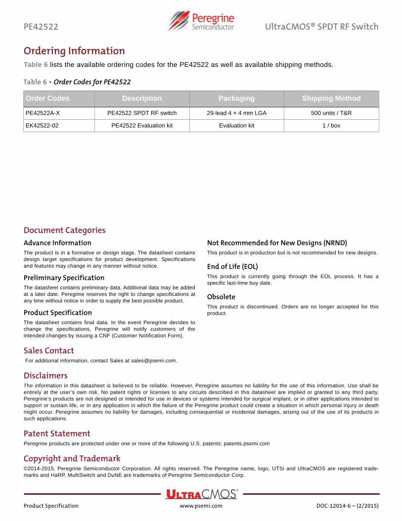
Ordering InformationTable 6 lists the available ordering codes for the PE42522 as well as available shipping methods.
Table 6 • Order Codes for PE42522
Order Codes Description Packaging Shipping Method
PE42522A-X PE42522 SPDT RF switch 29-lead 4 × 4 mm LGA 500 units / T&R
EK42522-02 PE42522 Evaluation kit Evaluation kit 1 / box
Product Specification www.psemi.com DOC-12014-6 – (2/2015)
Document CategoriesAdvance InformationThe product is in a formative or design stage. The datasheet containsdesign target specifications for product development. Specificationsand features may change in any manner without notice.
Preliminary SpecificationThe datasheet contains preliminary data. Additional data may be addedat a later date. Peregrine reserves the right to change specifications atany time without notice in order to supply the best possible product.
Product SpecificationThe datasheet contains final data. In the event Peregrine decides tochange the specifications, Peregrine will notify customers of theintended changes by issuing a CNF (Customer Notification Form).
Not Recommended for New Designs (NRND)This product is in production but is not recommended for new designs.
End of Life (EOL)This product is currently going through the EOL process. It has aspecific last-time buy date.
ObsoleteThis product is discontinued. Orders are no longer accepted for thisproduct.
Sales Contact For additional information, contact Sales at [email protected].
DisclaimersThe information in this datasheet is believed to be reliable. However, Peregrine assumes no liability for the use of this information. Use shall beentirely at the user’s own risk. No patent rights or licenses to any circuits described in this datasheet are implied or granted to any third party.Peregrine’s products are not designed or intended for use in devices or systems intended for surgical implant, or in other applications intended tosupport or sustain life, or in any application in which the failure of the Peregrine product could create a situation in which personal injury or deathmight occur. Peregrine assumes no liability for damages, including consequential or incidental damages, arising out of the use of its products insuch applications.
Patent StatementPeregrine products are protected under one or more of the following U.S. patents: patents.psemi.com
Copyright and Trademark©2014-2015, Peregrine Semiconductor Corporation. All rights reserved. The Peregrine name, logo, UTSi and UltraCMOS are registered trade-marks and HaRP, MultiSwitch and DuNE are trademarks of Peregrine Semiconductor Corp.
PE42522UltraCMOS® SPDT RF Switch
DOC-12014-6 – (2/2015) Page 25www.psemi.com