Embed Size (px)
Citation preview
PE42525 and PE426525Performance OptimizationApplication Note 66
SummaryThis application note provides the recommended landing pattern and assembly process for achieving optimum performance with the PE42525 and PE426525. The PE42525 and PE426525 are flip-chip, single-pole double-throw (SPDT) switches that support a wide frequency range from 9 kHz to 60 GHz. The PE42525 is suited for test and measurement (T&M), microwave backhaul, and radar and military communications (mil-comm) applications. The PE426525 is ideal for applications that require extended temperature support in the –55 °C to +125 °C range, such as harsh industrial applications.
IntroductionPE42525 and PE426525 are the first 60 GHz millimeter-wave switches to harness the high-frequency performance of UltraCMOS®. Monolithic microwave integrated circuit (MMIC) design techniques are used to achieve unprecedented performance in the K and Ka microwave and millimeter-wave bands. Achieving 1.9 dB of insertion loss and greater than 37 dB of isolation at 50 GHz, the PE42525 and PE426525 reflective SPDT switches deliver the same high-power, high-linearity performance for which Peregrine’s UltraCMOS technology is historically known.
Product OverviewThe PE42525 and PE426525 are flip-chip SPDT switches that use lead-free solder ball technology to provide the signal and ground interconnect. Solder reflow profiles common to lead-free surface-mount device (SMD) assembly can be readily used to achieve uniform and reliable attachment.
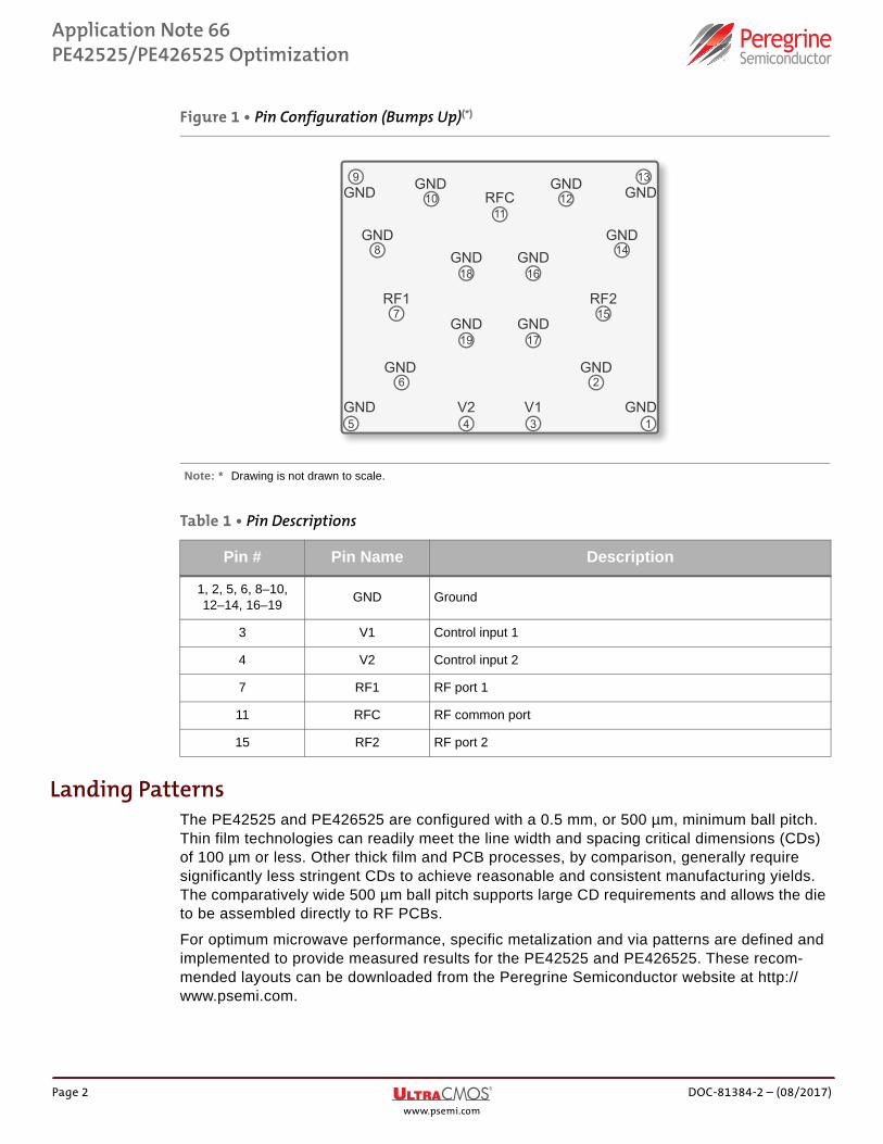
Figure 1 shows the pin configuration for the PE42525 and PE426525. Table 1 provides detailed pin descriptions. To ease routing and manufacturing, the pin configuration maintains a minimum of 500 µm (0.5 mm) pitch between all unique signal pads.
©2015-2017, Peregrine Semiconductor Corporation. All rights reserved. • Headquarters: 9380 Carroll Park Drive, San Diego, CA, 92121
Application Note DOC-81384-2 – (08/2017)www.psemi.com
Application Note 66PE42525/PE426525 Optimization
Landing PatternsThe PE42525 and PE426525 are configured with a 0.5 mm, or 500 µm, minimum ball pitch. Thin film technologies can readily meet the line width and spacing critical dimensions (CDs) of 100 µm or less. Other thick film and PCB processes, by comparison, generally require significantly less stringent CDs to achieve reasonable and consistent manufacturing yields. The comparatively wide 500 µm ball pitch supports large CD requirements and allows the die to be assembled directly to RF PCBs.
For optimum microwave performance, specific metalization and via patterns are defined and implemented to provide measured results for the PE42525 and PE426525. These recom-mended layouts can be downloaded from the Peregrine Semiconductor website at http://www.psemi.com.
Figure 1 • Pin Configuration (Bumps Up)(*)
Note: * Drawing is not drawn to scale.
Table 1 • Pin Descriptions
Pin # Pin Name Description
1, 2, 5, 6, 8–10, 12–14, 16–19
GND Ground
3 V1 Control input 1
4 V2 Control input 2
7 RF1 RF port 1
11 RFC RF common port
15 RF2 RF port 2
1345
9 13
15
14
1618
1719
1210
8
7
6
11
2
GNDV1V2GND
GND GND
GND
GND GND
GNDGND GND
GND
RF1 RF2
GND
GNDRFC GND
Page 2 DOC-81384-2 – (08/2017)www.psemi.com
Application Note 66PE42525/PE426525 Optimization
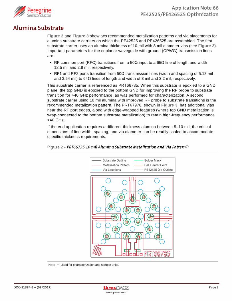
Alumina SubstrateFigure 2 and Figure 3 show two recommended metalization patterns and via placements for alumina substrate carriers on which the PE42525 and PE426525 are assembled. The first substrate carrier uses an alumina thickness of 10 mil with 8 mil diameter vias (see Figure 2). Important parameters for the coplanar waveguide with ground (CPWG) transmission lines are:
• RF common port (RFC) transitions from a 50Ω input to a 65Ω line of length and width 12.5 mil and 2.8 mil, respectively.
• RF1 and RF2 ports transition from 50Ω transmission lines (width and spacing of 5.13 mil and 3.54 mil) to 64Ω lines of length and width of 8 mil and 3.2 mil, respectively.
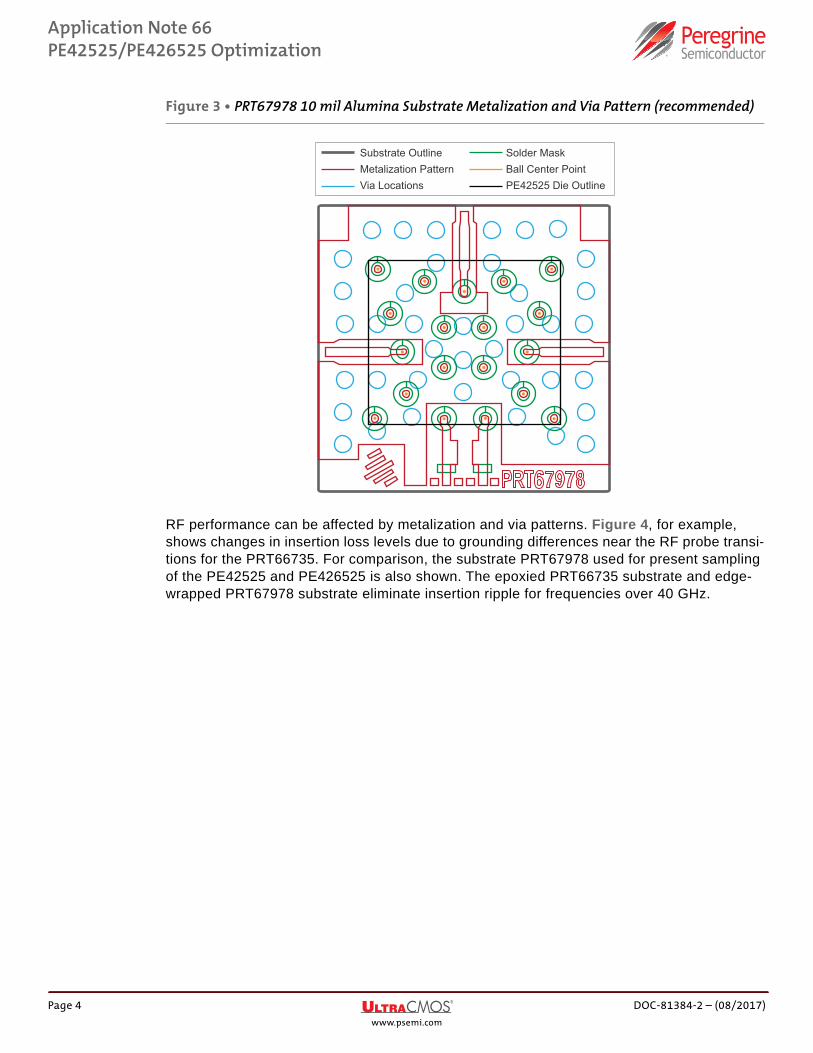
This substrate carrier is referenced as PRT66735. When this substrate is epoxied to a GND plane, the top GND is epoxied to the bottom GND for improving the RF probe to substrate transition for >40 GHz performance, as was performed for characterization. A second substrate carrier using 10 mil alumina with improved RF probe to substrate transitions is the recommended metalization pattern. The PRT67978, shown in Figure 3, has additional vias near the RF port edges, along with edge-wrapped features (where top GND metalization is wrap-connected to the bottom substrate metalization) to retain high-frequency performance >40 GHz.
If the end application requires a different thickness alumina between 5–10 mil, the critical dimensions of line width, spacing, and via diameter can be readily scaled to accommodate specific thickness requirements.
Figure 2 • PRT66735 10 mil Alumina Substrate Metalization and Via Pattern(*)
Note: * Used for characterization and sample units.
Substrate OutlineMetalization PatternVia Locations
Solder MaskBall Center PointPE42525 Die Outline
DOC-81384-2 – (08/2017) Page 3www.psemi.com
Application Note 66PE42525/PE426525 Optimization
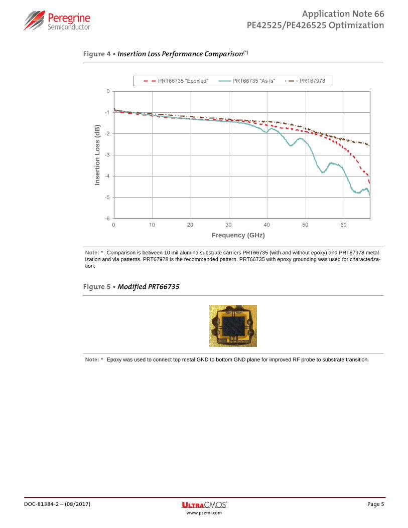
RF performance can be affected by metalization and via patterns. Figure 4, for example, shows changes in insertion loss levels due to grounding differences near the RF probe transi-tions for the PRT66735. For comparison, the substrate PRT67978 used for present sampling of the PE42525 and PE426525 is also shown. The epoxied PRT66735 substrate and edge-wrapped PRT67978 substrate eliminate insertion ripple for frequencies over 40 GHz.
Figure 3 • PRT67978 10 mil Alumina Substrate Metalization and Via Pattern (recommended)
Substrate OutlineMetalization PatternVia Locations
Solder MaskBall Center PointPE42525 Die Outline
Page 4 DOC-81384-2 – (08/2017)www.psemi.com
Application Note 66PE42525/PE426525 Optimization
Figure 4 • Insertion Loss Performance Comparison(*)
Note: * Comparison is between 10 mil alumina substrate carriers PRT66735 (with and without epoxy) and PRT67978 metal-ization and via patterns. PRT67978 is the recommended pattern. PRT66735 with epoxy grounding was used for characteriza-tion.
Figure 5 • Modified PRT66735
Note: * Epoxy was used to connect top metal GND to bottom GND plane for improved RF probe to substrate transition.
-6
-5
-4
-3
-2
-1
0
0 10 20 30 40 50 60
Inse
rtio
n Lo
ss (d
B)
Frequency (GHz)
PRT66735 "Epoxied" PRT66735 "As Is" PRT67978
DOC-81384-2 – (08/2017) Page 5www.psemi.com
Application Note 66PE42525/PE426525 Optimization
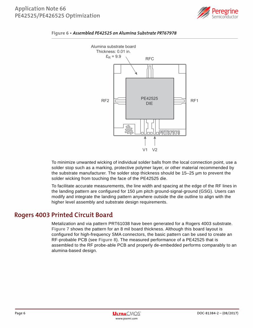
To minimize unwanted wicking of individual solder balls from the local connection point, use a solder stop such as a marking, protective polymer layer, or other material recommended by the substrate manufacturer. The solder stop thickness should be 15–25 µm to prevent the solder wicking from touching the face of the PE42525 die.
To facilitate accurate measurements, the line width and spacing at the edge of the RF lines in the landing pattern are configured for 150 µm pitch ground-signal-ground (GSG). Users can modify and integrate the landing pattern anywhere outside the die outline to align with the higher level assembly and substrate design requirements.
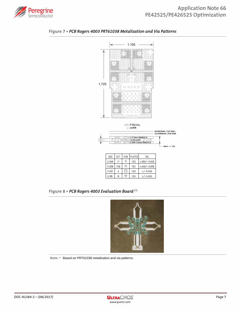
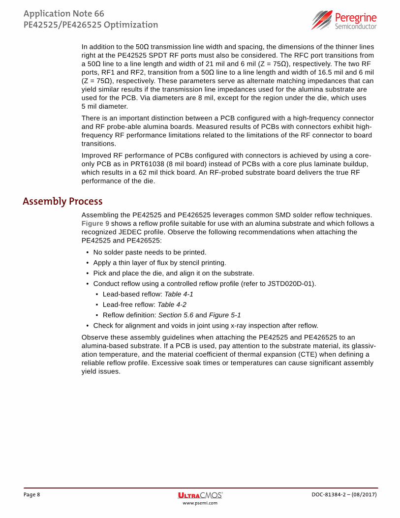
Rogers 4003 Printed Circuit BoardMetalization and via pattern PRT61038 have been generated for a Rogers 4003 substrate. Figure 7 shows the pattern for an 8 mil board thickness. Although this board layout is configured for high-frequency SMA connectors, the basic pattern can be used to create an RF-probable PCB (see Figure 8). The measured performance of a PE42525 that is assembled to the RF probe-able PCB and properly de-embedded performs comparably to an alumina-based design.
Figure 6 • Assembled PE42525 on Alumina Substrate PRT67978
PE42525DIE
V1 V2
Alumina substrate boardThickness: 0.01 in.
ƐR = 9.9
RF2 RF1
RFC
Page 6 DOC-81384-2 – (08/2017)www.psemi.com
Application Note 66PE42525/PE426525 Optimization
Figure 7 • PCB Rogers 4003 PRT61038 Metalization and Via Patterns
Figure 8 • PCB Rogers 4003 Evaluation Board (*)
Note: * Based on PRT61038 metalization and via patterns.
1.100
1.725
DOC-81384-2 – (08/2017) Page 7www.psemi.com
Application Note 66PE42525/PE426525 Optimization
In addition to the 50Ω transmission line width and spacing, the dimensions of the thinner lines right at the PE42525 SPDT RF ports must also be considered. The RFC port transitions from a 50Ω line to a line length and width of 21 mil and 6 mil (Z = 75Ω), respectively. The two RF ports, RF1 and RF2, transition from a 50Ω line to a line length and width of 16.5 mil and 6 mil (Z = 75Ω), respectively. These parameters serve as alternate matching impedances that can yield similar results if the transmission line impedances used for the alumina substrate are used for the PCB. Via diameters are 8 mil, except for the region under the die, which uses 5 mil diameter.
There is an important distinction between a PCB configured with a high-frequency connector and RF probe-able alumina boards. Measured results of PCBs with connectors exhibit high-frequency RF performance limitations related to the limitations of the RF connector to board transitions.
Improved RF performance of PCBs configured with connectors is achieved by using a core-only PCB as in PRT61038 (8 mil board) instead of PCBs with a core plus laminate buildup, which results in a 62 mil thick board. An RF-probed substrate board delivers the true RF performance of the die.
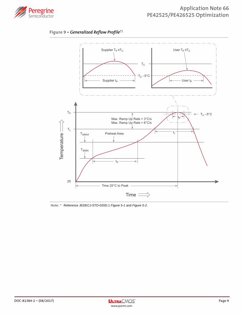
Assembly ProcessAssembling the PE42525 and PE426525 leverages common SMD solder reflow techniques. Figure 9 shows a reflow profile suitable for use with an alumina substrate and which follows a recognized JEDEC profile. Observe the following recommendations when attaching the PE42525 and PE426525:
• No solder paste needs to be printed.
• Apply a thin layer of flux by stencil printing.
• Pick and place the die, and align it on the substrate.
• Conduct reflow using a controlled reflow profile (refer to JSTD020D-01).
Lead-based reflow: Table 4-1
Lead-free reflow: Table 4-2
Reflow definition: Section 5.6 and Figure 5-1
• Check for alignment and voids in joint using x-ray inspection after reflow.
Observe these assembly guidelines when attaching the PE42525 and PE426525 to an alumina-based substrate. If a PCB is used, pay attention to the substrate material, its glassiv-ation temperature, and the material coefficient of thermal expansion (CTE) when defining a reliable reflow profile. Excessive soak times or temperatures can cause significant assembly yield issues.
Page 8 DOC-81384-2 – (08/2017)www.psemi.com
Application Note 66PE42525/PE426525 Optimization
Figure 9 • Generalized Reflow Profile(*)
Note: * Reference JEDECJ-STD-020D.1 Figure 5-1 and Figure 5-2.
TC
Supplier tP User tP
User TP ≤TCSupplier TP ≤TC
TC –5°C
TC –5°C TP
TL
Time 25°C to Peak
Tem
pera
ture
Time
25
tLTSMAX Preheat Area
Max. Ramp Up Rate = 3°C/sMax. Ramp Up Rate = 6°C/s
TSMIN
tS
tP
DOC-81384-2 – (08/2017) Page 9www.psemi.com
Application Note 66PE42525/PE426525 Optimization
Recommendations for Attaching the PE42525 and PE426525 on a PCBWhen defining a reliable reflow profile, pay attention to the PCB substrate material, its glassivation temperature, and the various CTEs. Excessive soak times or temperatures can cause significant assembly yield issues and potentially laminate delamination.
Table 2 through Table 4 list assembly-related process parameters that can help define an assembly flow for specific high-frequency PCB substrates. When refining a suitable reflow profile and assembly process, also consider other components on the same PCB, the PCB substrate temperature limitations, and the PCB board design and its thermal properties.
Table 2 • PE42525 and PE426525 Assembly-Related Parameters
ParameterPE42525 and
PE426525Unit Comments
Max reflow temperature, TP ≥260 °C JEDEC J-STD-020D.1 Table 4-2
Max dwell at TP 10 sec JEDEC J-STD-020D.1 Table 5-2
Recommended flux
Pb-free solder ballTin-95.5/Ag-3.5/
Cu-1 (%)SAC 351 solder definition
Min landing size 90 µm
Solder stop max thickness 25 µm
Solder stop diameter 190 µm
Solder paste particle size Type 5 15–25 µm particle size
Stencil thickness 60 µm
Stencil aperture diameter 180 µm
CTE (worst case X, Y, Z) 6–7 ppm/°C
UnderfillNot
recommendedIf deemed necessary, a low loss, low dielectric constant underfill is recommended.
Table 3 • Assembly Related Parameters for Common High-Frequency PCB Substrates
ParameterPanasonic Megtron 6
Rogers 4350 Rogers 4003 Unit
Max reflow temperature, TP ≥260 ≥260 ≥260 °C
Max dwell at TP 10 10 10 sec
Glassivation temperature, TG 180–210 >280 >280 °C
CTE (worst case X, Y, Z)
X 10 11 ppm/°C
Y 12 14
Z 45 32 46
Page 10 DOC-81384-2 – (08/2017)www.psemi.com
Application Note 66PE42525/PE426525 Optimization
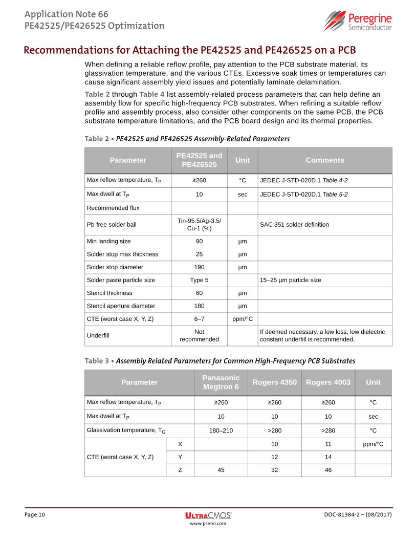
Table 4 • Reflow Profile Parameter Recommendations(*)
ParameterPb-free
AssemblyUnit Comments
Preheat temperature 150–200 °C
Preheat time 60–120 sec
Ramp up rate 3 °C/sec
Liquidous temperature, TL 217 °C SAC 351 melting point
Time above TL 60–150 sec
Peak temperature, TP 260 °C
Time within 5 °C of TP 10–30 sec
Time 25 °C to TP 6–8 min
Ramp down rate 3–6 °C/sec
Note: * Source is JEDEC J-STD-020E.
Figure 10 • Suggested Starting Definition for PCB Reflow Profile
Tem
pera
ture
Time6–8 minutes
60–120 seconds
+260 °C
+217 °C
+25 °C
60–150seconds
10–30 seconds
+255 °C
Max ramp up rate = 3 °C/sMax ramp down rate = 6 °C/s
Preheat area
+200 °C
+150 °C
DOC-81384-2 – (08/2017) Page 11www.psemi.com
Application Note 66PE42525/PE426525 Optimization
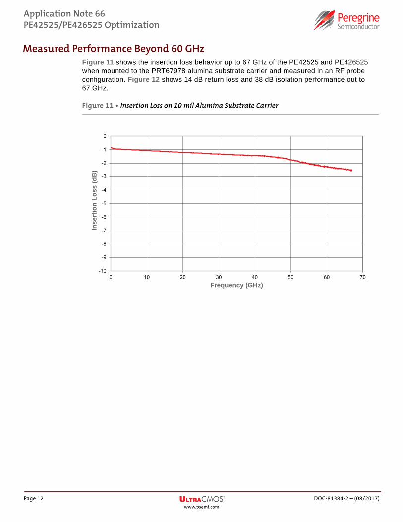
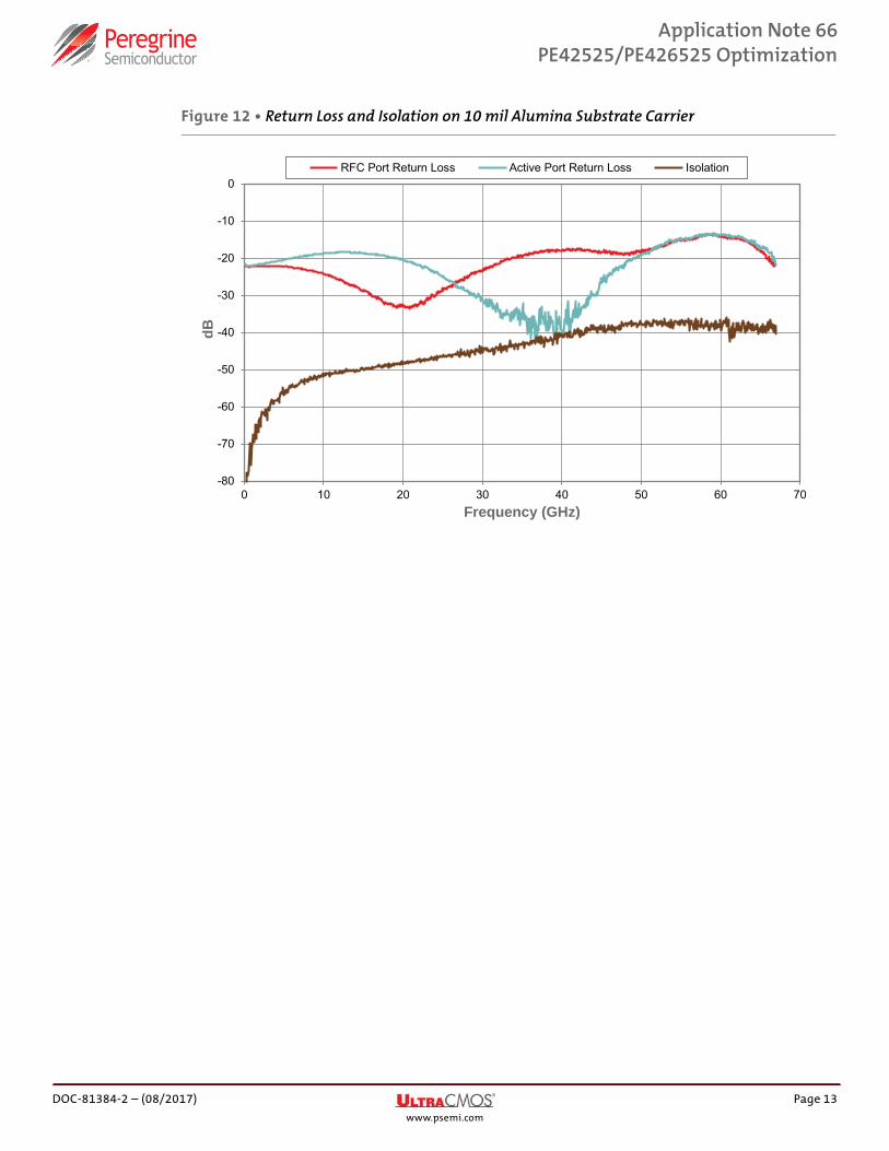
Measured Performance Beyond 60 GHzFigure 11 shows the insertion loss behavior up to 67 GHz of the PE42525 and PE426525 when mounted to the PRT67978 alumina substrate carrier and measured in an RF probe configuration. Figure 12 shows 14 dB return loss and 38 dB isolation performance out to 67 GHz.
Figure 11 • Insertion Loss on 10 mil Alumina Substrate Carrier
-10
-9
-8
-7
-6
-5
-4
-3
-2
-1
0
0 10 20 30 40 50 60 70
Inse
rtio
n Lo
ss (d
B)
Frequency (GHz)
Page 12 DOC-81384-2 – (08/2017)www.psemi.com
Application Note 66PE42525/PE426525 Optimization
Figure 12 • Return Loss and Isolation on 10 mil Alumina Substrate Carrier
-80
-70
-60
-50
-40
-30
-20
-10
0
0 10 20 30 40 50 60 70
dB
Frequency (GHz)
RFC Port Return Loss Active Port Return Loss Isolation
DOC-81384-2 – (08/2017) Page 13www.psemi.com
Application Note 66PE42525/PE426525 Optimization
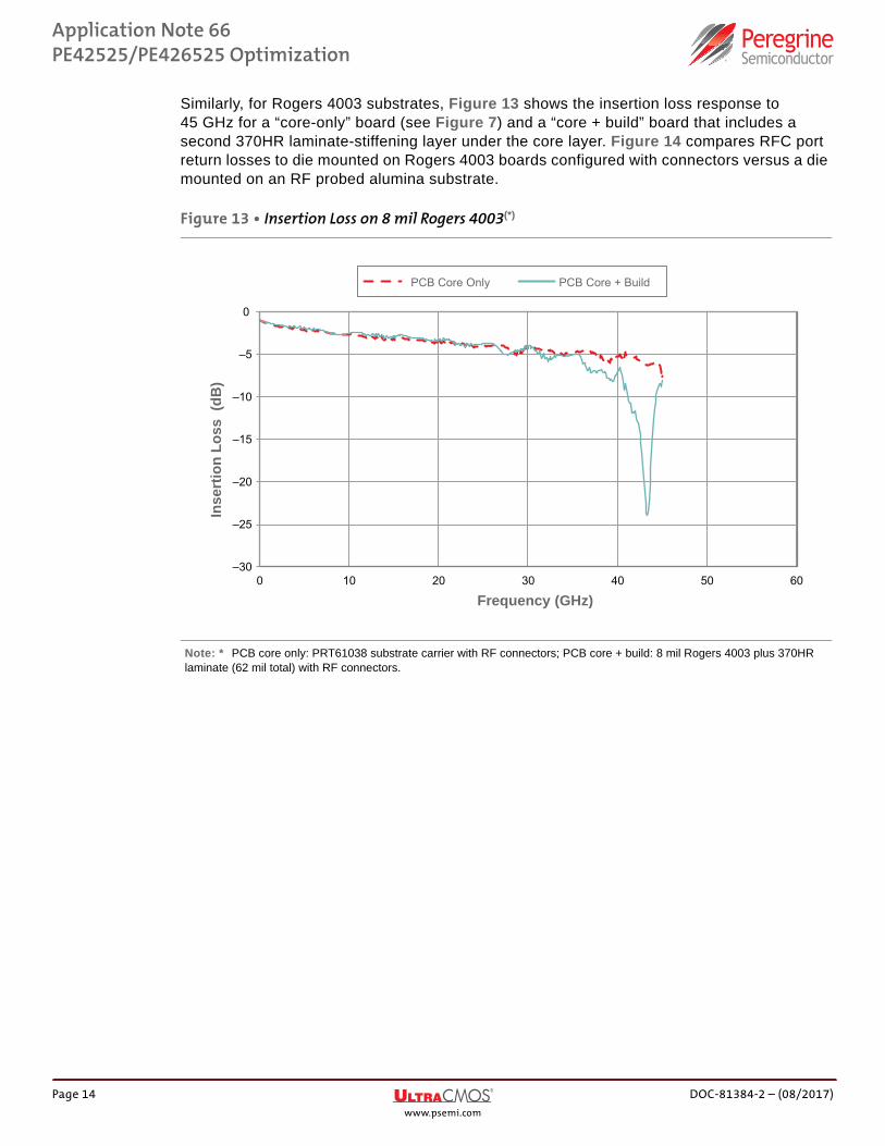
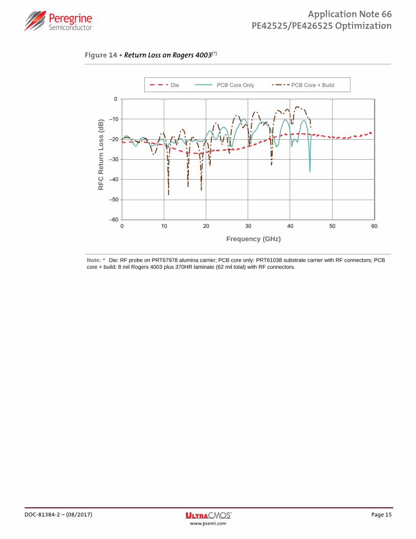
Similarly, for Rogers 4003 substrates, Figure 13 shows the insertion loss response to 45 GHz for a “core-only” board (see Figure 7) and a “core + build” board that includes a second 370HR laminate-stiffening layer under the core layer. Figure 14 compares RFC port return losses to die mounted on Rogers 4003 boards configured with connectors versus a die mounted on an RF probed alumina substrate.
Figure 13 • Insertion Loss on 8 mil Rogers 4003(*)
Note: * PCB core only: PRT61038 substrate carrier with RF connectors; PCB core + build: 8 mil Rogers 4003 plus 370HR laminate (62 mil total) with RF connectors.
–30
–25
–20
–15
–10
–5
0
0 10 20 30 40 50 60
Inse
rtio
n Lo
ss (
dB)
Frequency (GHz)
PCB Core Only PCB Core + Build
Page 14 DOC-81384-2 – (08/2017)www.psemi.com
Application Note 66PE42525/PE426525 Optimization
Figure 14 • Return Loss on Rogers 4003(*)
Note: * Die: RF probe on PRT67978 alumina carrier; PCB core only: PRT61038 substrate carrier with RF connectors; PCB core + build: 8 mil Rogers 4003 plus 370HR laminate (62 mil total) with RF connectors.
–60
–50
–40
–30
–20
–10
0
0 10 20 30 40 50 60
RFC
Ret
urn
Loss
(dB
)
Frequency (GHz)
Die PCB Core Only PCB Core + Build
DOC-81384-2 – (08/2017) Page 15www.psemi.com
DOC-81384-2 PE42525/PE426525 Optimization
ConclusionPE42525 and PE426525 are the newest millimeter-wave switches from Peregrine Semicon-ductor. Both switches deliver competitive insertion loss, exceptional isolation, and high linearity and power handling, along with the uniformity and availability that UltraCMOS affords. To achieve high performance at these frequencies, however, extreme care must be taken to eliminate stray parasitics affecting the RF channel.
The guidelines and best practices in this application note enable users to obtain optimum performance from the PE42525 and PE426525. It includes descriptions of landing patterns in different substrate technologies, which show comparable performance up to 60 GHz. Complete CAD files of the physical layouts are available from Peregrine website to help integrate the PE42525 and PE426525 into higher-level assemblies and systems.
Application Note www.psemi.com DOC-81384-2 – (08/2017)
Sales ContactFor additional information, contact Sales at [email protected].
DisclaimersThe information in this document is believed to be reliable. However, Peregrine assumes no liability for the use of this information. Use shall beentirely at the user’s own risk. No patent rights or licenses to any circuits described in this document are implied or granted to any third party.Peregrine’s products are not designed or intended for use in devices or systems intended for surgical implant, or in other applications intended tosupport or sustain life, or in any application in which the failure of the Peregrine product could create a situation in which personal injury or deathmight occur. Peregrine assumes no liability for damages, including consequential or incidental damages, arising out of the use of its products insuch applications.
Patent StatementPeregrine products are protected under one or more of the following U.S. patents: patents.psemi.com
Copyright and Trademark©2015-2017, Peregrine Semiconductor Corporation. All rights reserved. The Peregrine name, logo, UTSi and UltraCMOS are registered trade-marks and HaRP, MultiSwitch and DuNE are trademarks of Peregrine Semiconductor Corp.