Embed Size (px)
Citation preview
Copyright © 2017 Raytheon Company. All rights reserved.
Assessment of Copper Bond Wire for Use in
Long Term Military Applications
Integrated Defense SystemsKen Rispoli
Aaron Lecomte - Presenter
Aaron DerMarderosian
eTPCR: IDS-11029
05/10/2017Approved for Public Release
This document does not contain technology or technical data controlled under either the U.S. International Traffic in Arms Regulations or the U.S. Export Administration Regulations.
2
Copper Wire Bonding Intro Primary industry methods of wire bonding include Gold (Au), Aluminum (Al), and Copper (Cu)
Gold wire bonds have been the ideal choice for decades, however Copper is taking over
– Copper advantages vs. Au & Al
More economical
Lower electrical resistance
Higher thermal conductivity
Higher yield strength
– Copper disadvantages vs. Au & Al
Prone to oxidation
Need for forming gas complicates bonding
Hardness and brittleness of Cu can cause cratering during bonding
Technology relatively new compared to Au wire
Commercial industries are transitioning to copper wire due to lower material cost
and higher electrical and thermal performanceApproved for Public Release
This document does not contain technology or technical data controlled under either the U.S. International Traffic in Arms Regulations or the U.S. Export Administration Regulations.
3
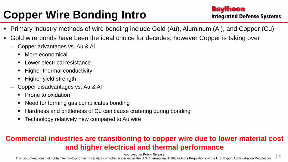
Wire Bonding
Copper Wire Bonding Gold Wire Bonding
Approved for Public Release
This document does not contain technology or technical data controlled under either the U.S. International Traffic in Arms Regulations or the U.S. Export Administration Regulations.
4
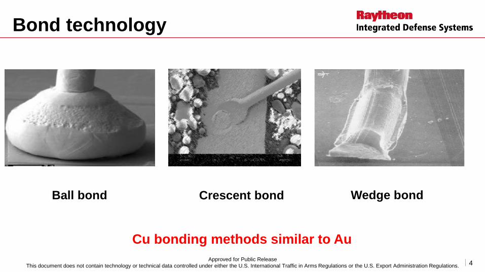
Bond technology
Cu bonding methods similar to Au
Ball bond Wedge bondCrescent bond
Approved for Public Release
This document does not contain technology or technical data controlled under either the U.S. International Traffic in Arms Regulations or the U.S. Export Administration Regulations.
5
Potential Failure Modes / Risks
Potential failure points
A) Ball bond
B) Wire
C) Wedge bond
Ball die pad
bondCrescent
package
post bond
Copper / Aluminum Bond
Intermetallic Region
Gold / Aluminum Bond Intermetallic Region
Copper wire assembly, electrical performance & reliability presents significant reliability risks compared
to legacy gold wire
Failure Modes Reliability Risks
1) Corrosion Loss of electrical connection over time and with humidity
2) Intermetallic growth Loss of electrical connection over time and with temperature
3) Process variability – bondability from copper oxidation Potential loss of bond integrity
4) No standard test method or requirements for copper – Military Standard Au / Al This could lead to variability in manufacturer quality and inconsistent results from
destructive physical analysis (DPA) assessment
5) Susceptibility to cleaning process chemicals Commercial grade component intended for "no clean" SMT could be put at risk
when processed in a DoD application requiring post solder cleaning
6) Epoxy compounds such as flame retardants have been shown to increase
susceptibility of copper to corrosion
Impact of encapsulant chemistry: Transition to copper without assessing package
material could impact long term life of copper wire integrity (Bromines, etc.)
7) Package removal methods may affect copper wire and impact follow on
assessment
Standard DPA plastic removal processes required to insure Cu wire integrity is
maintained for follow on mechanical integrity and inter-metallic assessment
8) Bonding with copper wire requires greater strike force due to material hardness Potential damage to die and circuitry under the pad may require design modification
to pad & metallization effecting performance
9) Change in electrical performance Change from Al to Cu in RF IC's are subject to parametric shifts and potential noise
susceptibility
10) Some commercial suppliers transitioned to copper without changing part
number or adding an identifier
Loss of technology traceability potentially obscures performance failure issues in
legacy designs
Approved for Public Release
This document does not contain technology or technical data controlled under either the U.S. International Traffic in Arms Regulations or the U.S. Export Administration Regulations.
6
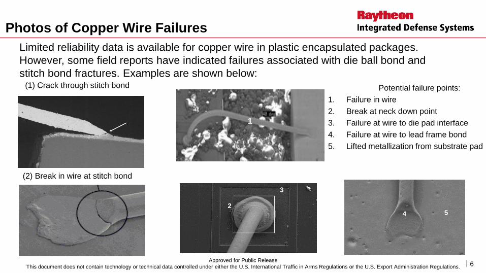
(2) Break in wire at stitch bond
(1) Crack through stitch bond Potential failure points:
1. Failure in wire
2. Break at neck down point
3. Failure at wire to die pad interface
4. Failure at wire to lead frame bond
5. Lifted metallization from substrate pad
Photos of Copper Wire Failures
3
4
1
25
Limited reliability data is available for copper wire in plastic encapsulated packages.
However, some field reports have indicated failures associated with die ball bond and
stitch bond fractures. Examples are shown below:
Approved for Public Release
This document does not contain technology or technical data controlled under either the U.S. International Traffic in Arms Regulations or the U.S. Export Administration Regulations.
7
DPA Wire Bond Assessment Test Plan1. X-ray
2. CSAM – IPC/JEDEC J-STD-035 Acoustic Microscopy for Non-Hermetic Encapsulated Electronic Components
3. Electrical Continuity - I/O’s with respect to Power & Ground pins
4. Environmental conditioning, per J-STD-020a) Bake the sample for 24 hours minimum at 125 +5 / -0 °C, per J-STD-020, Section 5.4. This step is intended to
remove moisture from the package so that it will be ‘‘dry.’’
b) Devices placed in a clean, dry, shallow container so that the package bodies do not touch or overlap each other. Samples subjected to 168 +5/-0 hours of 85 °C/85% RH environmental conditioning, per J-STD-020, Section 5.5
c) 100 temperature cycles, Condition B, JEDEC JESD22-A104 -55C / +125C. Minimum 10 minute soak time at maximum and minimum soak temperatures
d) 3 cycles of SMT solder reflow per paragraph 5.6 and Table 5-2 of J-STD-020. Reflow is performed not sooner than 15 minutes and not longer than 4 hours after removal from the temperature/humidity chamber
5. De-cap microwave plasma oxygen etch
6. Bond visual inspection
7. Bond integrity a) Destructive wire bond pull per MIL-STD-883 Method 2011 gold wire limits
b) Destructive ball shear per JEDEC JESD22-B116
8. Bond cross sectioning & material analysisa) Ball to die pad bond
b) Crescent to package post bond
Approved for Public Release
This document does not contain technology or technical data controlled under either the U.S. International Traffic in Arms Regulations or the U.S. Export Administration Regulations.
8
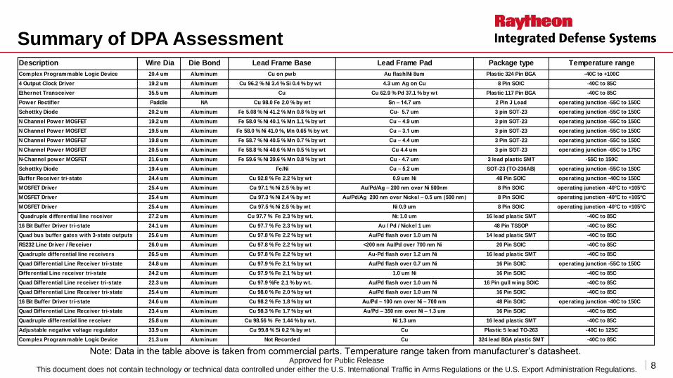
Summary of DPA AssessmentDescription Wire Dia Die Bond Lead Frame Base Lead Frame Pad Package type Temperature range
Complex Programmable Logic Device 20.4 um Aluminum Cu on pwb Au flash/Ni 8um Plastic 324 Pin BGA -40C to +100C
4 Output Clock Driver 19.2 um Aluminum Cu 96.2 % Ni 3.4 % Si 0.4 % by wt 4.3 um Ag on Cu 8 Pin SOIC -40C to 85C
Ethernet Transceiver 35.5 um Aluminum Cu Cu 62.9 % Pd 37.1 % by wt Plastic 117 Pin BGA -40C to 85C
Power Rectifier Paddle NA Cu 98.0 Fe 2.0 % by wt Sn – 14.7 um 2 Pin J Lead operating junction -55C to 150C
Schottky Diode 20.2 um Aluminum Fe 5.08 % Ni 41.2 % Mn 0.8 % by wt Cu- 5.7 um 3 pin SOT-23 operating junction -55C to 150C
N Channel Power MOSFET 19.2 um Aluminum Fe 58.0 % Ni 40.1 % Mn 1.1 % by wt Cu – 4.9 um 3 pin SOT-23 operating junction -55C to 150C
N Channel Power MOSFET 19.5 um Aluminum Fe 58.0 % Ni 41.0 %, Mn 0.65 % by wt Cu – 3.1 um 3 pin SOT-23 operating junction -55C to 150C
N Channel Power MOSFET 19.8 um Aluminum Fe 58.7 % Ni 40.5 % Mn 0.7 % by wt Cu – 4.4 um 3 Pin SOT-23 operating junction -55C to 150C
N Channel Power MOSFET 20.5 um Aluminum Fe 58.8 % Ni 40.6 % Mn 0.5 % by wt Cu 4.4 um 3 pin SOT-23 operating junction -65C to 175C
N-Channel power MOSFET 21.6 um Aluminum Fe 59.6 % Ni 39.6 % Mn 0.8 % by wt Cu - 4.7 um 3 lead plastic SMT -55C to 150C
Schottky Diode 19.4 um Aluminum Fe/Ni Cu – 5.2 um SOT-23 (TO-236AB) operating junction -55C to 150C
Buffer Receiver tri-state 24.4 um Aluminum Cu 92.8 % Fe 2.2 % by wt 0.9 um Ni 48 Pin SOIC operating junction -40C to 150C
MOSFET Driver 25.4 um Aluminum Cu 97.1 % Ni 2.5 % by wt Au/Pd/Ag – 200 nm over Ni 500nm 8 Pin SOIC operating junction -40°C to +105°C
MOSFET Driver 25.4 um Aluminum Cu 97.3 % Ni 2.4 % by wt Au/Pd/Ag 200 nm over Nickel – 0.5 um (500 nm) 8 Pin SOIC operating junction -40°C to +105°C
MOSFET Driver 25.4 um Aluminum Cu 97.5 % Ni 2.5 % by wt Ni 0.9 um 8 Pin SOIC operating junction -40°C to +105°C
Quadruple differential line receiver 27.2 um Aluminum Cu 97.7 % Fe 2.3 % by wt. Ni: 1.0 um 16 lead plastic SMT -40C to 85C
16 Bit Buffer Driver tri-state 24.1 um Aluminum Cu 97.7 % Fe 2.3 % by wt Au / Pd / Nickel 1 um 48 Pin TSSOP -40C to 85C
Quad bus buffer gates with 3-state outputs 25.6 um Aluminum Cu 97.8 % Fe 2.2 % by wt Au/Pd flash over 1.0 um Ni 14 lead plastic SMT -40C to 85C
RS232 Line Driver / Receiver 26.0 um Aluminum Cu 97.8 % Fe 2.2 % by wt <200 nm Au/Pd over 700 nm Ni 20 Pin SOIC -40C to 85C
Quadruple differential line receivers 26.5 um Aluminum Cu 97.8 % Fe 2.2 % by wt Au-Pd flash over 1.2 um Ni 16 lead plastic SMT -40C to 85C
Quad Differential Line Receiver tri-state 24.8 um Aluminum Cu 97.9 % Fe 2.1 % by wt Au/Pd flash over 0.7 um Ni 16 Pin SOIC operating junction -55C to 150C
Differential Line receiver tri-state 24.2 um Aluminum Cu 97.9 % Fe 2.1 % by wt 1.0 um Ni 16 Pin SOIC -40C to 85C
Quad Differential Line receiver tri-state 22.3 um Aluminum Cu 97.9 % Fe 2.1 % by wt. Au/Pd flash over 1.0 um Ni 16 Pin gull w ing SOIC -40C to 85C
Quad Differential Line Receiver tri-state 25.4 um Aluminum Cu 98.0 % Fe 2.0 % by wt Au/Pd flash over 1.0 um Ni 16 Pin SOIC -40C to 85C
16 Bit Buffer Driver tri-state 24.6 um Aluminum Cu 98.2 % Fe 1.8 % by wt Au/Pd – 100 nm over Ni – 700 nm 48 Pin SOIC operating junction -40C to 150C
Quad Differential Line Receiver tri-state 23.4 um Aluminum Cu 98.3 % Fe 1.7 % by wt Au/Pd – 350 nm over Ni – 1.3 um 16 Pin SOIC -40C to 85C
Quadruple differential line receiver 25.8 um Aluminum Cu 98.56 % Fe 1.44 % by wt. Ni 1.3 um 16 lead plastic SMT -40C to 85C
Adjustable negative voltage regulator 33.9 um Aluminum Cu 99.8 % Si 0.2 % by wt Cu Plastic 5 lead TO-263 -40C to 125C
Complex Programmable Logic Device 21.3 um Aluminum Not Recorded Cu 324 lead BGA plastic SMT -40C to 85C
Note: Data in the table above is taken from commercial parts. Temperature range taken from manufacturer’s datasheet.Approved for Public Release
This document does not contain technology or technical data controlled under either the U.S. International Traffic in Arms Regulations or the U.S. Export Administration Regulations.
9
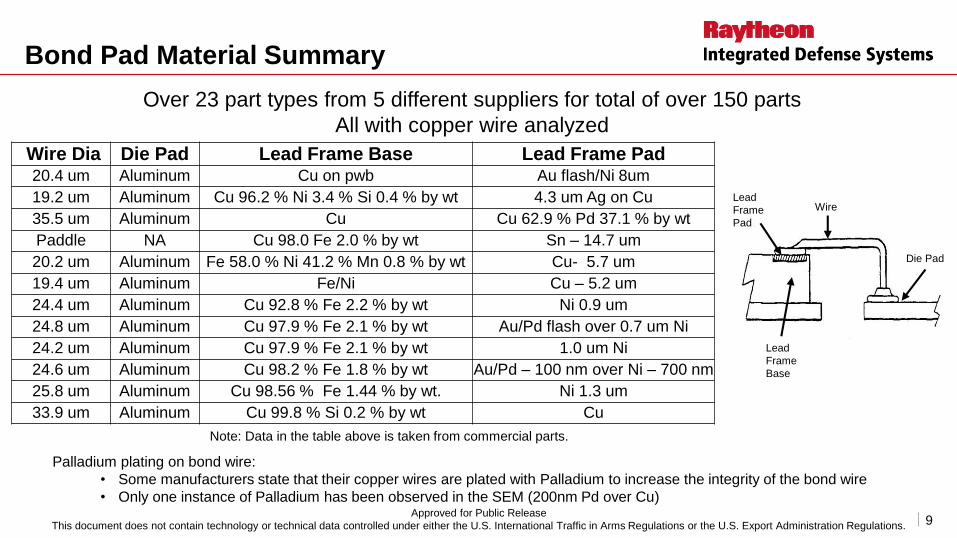
Bond Pad Material Summary
Wire Dia Die Pad Lead Frame Base Lead Frame Pad20.4 um Aluminum Cu on pwb Au flash/Ni 8um
19.2 um Aluminum Cu 96.2 % Ni 3.4 % Si 0.4 % by wt 4.3 um Ag on Cu
35.5 um Aluminum Cu Cu 62.9 % Pd 37.1 % by wt
Paddle NA Cu 98.0 Fe 2.0 % by wt Sn – 14.7 um
20.2 um Aluminum Fe 58.0 % Ni 41.2 % Mn 0.8 % by wt Cu- 5.7 um
19.4 um Aluminum Fe/Ni Cu – 5.2 um
24.4 um Aluminum Cu 92.8 % Fe 2.2 % by wt Ni 0.9 um
24.8 um Aluminum Cu 97.9 % Fe 2.1 % by wt Au/Pd flash over 0.7 um Ni
24.2 um Aluminum Cu 97.9 % Fe 2.1 % by wt 1.0 um Ni
24.6 um Aluminum Cu 98.2 % Fe 1.8 % by wt Au/Pd – 100 nm over Ni – 700 nm
25.8 um Aluminum Cu 98.56 % Fe 1.44 % by wt. Ni 1.3 um
33.9 um Aluminum Cu 99.8 % Si 0.2 % by wt Cu
Over 23 part types from 5 different suppliers for total of over 150 parts
All with copper wire analyzed
Palladium plating on bond wire:
• Some manufacturers state that their copper wires are plated with Palladium to increase the integrity of the bond wire
• Only one instance of Palladium has been observed in the SEM (200nm Pd over Cu)
Die Pad
Lead
Frame
Base
Lead
Frame
Pad
Wire
Approved for Public Release
This document does not contain technology or technical data controlled under either the U.S. International Traffic in Arms Regulations or the U.S. Export Administration Regulations.
Note: Data in the table above is taken from commercial parts.
10
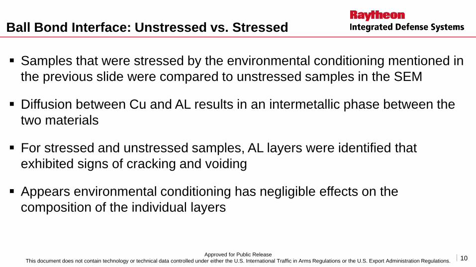
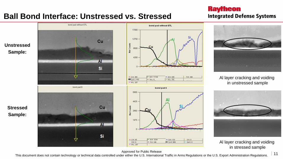
Ball Bond Interface: Unstressed vs. Stressed
Samples that were stressed by the environmental conditioning mentioned in
the previous slide were compared to unstressed samples in the SEM
Diffusion between Cu and AL results in an intermetallic phase between the
two materials
For stressed and unstressed samples, AL layers were identified that
exhibited signs of cracking and voiding
Appears environmental conditioning has negligible effects on the
composition of the individual layers
Approved for Public Release
This document does not contain technology or technical data controlled under either the U.S. International Traffic in Arms Regulations or the U.S. Export Administration Regulations.
11
Ball Bond Interface: Unstressed vs. Stressed
Unstressed
Sample:
Stressed
Sample:
Al layer cracking and voiding
in unstressed sample
Al layer cracking and voiding
in stressed sampleApproved for Public Release
This document does not contain technology or technical data controlled under either the U.S. International Traffic in Arms Regulations or the U.S. Export Administration Regulations.
12
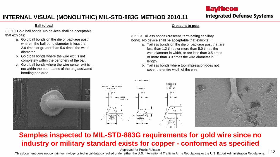
INTERNAL VISUAL (MONOLITHIC) MIL-STD-883G METHOD 2010.11
A2015-01459
Ball to pad
3.2.1.1 Gold ball bonds. No devices shall be acceptable
that exhibits:
a. Gold ball bonds on the die or package post
wherein the ball bond diameter is less than
2.0 times or greater than 5.0 times the wire
diameter.
b. Gold ball bonds where the wire exit is not
completely within the periphery of the ball.
c. Gold ball bonds where the wire center exit is
not within the boundaries of the unglassivated
bonding pad area.
Crescent to post
A2015-01459
3.2.1.3 Tailless bonds (crescent, terminating capillary
bond). No device shall be acceptable that exhibits:
a. Tailless bonds on the die or package post that are
less than 1.2 times or more than 5.0 times the
wire diameter in width, or are less than 0.5 times
or more than 3.0 times the wire diameter in
length.
b. Tailless bonds where tool impression does not
cover the entire width of the wire.
Samples inspected to MIL-STD-883G requirements for gold wire since no
industry or military standard exists for copper - conformed as specified Approved for Public Release
This document does not contain technology or technical data controlled under either the U.S. International Traffic in Arms Regulations or the U.S. Export Administration Regulations.
13
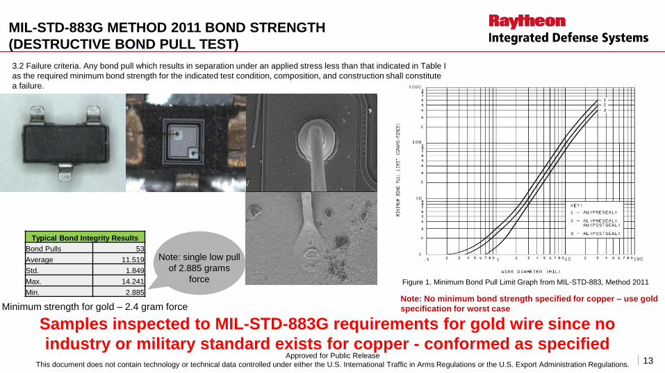
MIL-STD-883G METHOD 2011 BOND STRENGTH
(DESTRUCTIVE BOND PULL TEST)
Typical Bond Integrity Results
Bond Pulls 53
Average 11.519
Std. 1.849
Max. 14.241
Min. 2.885
3.2 Failure criteria. Any bond pull which results in separation under an applied stress less than that indicated in Table I
as the required minimum bond strength for the indicated test condition, composition, and construction shall constitute
a failure.
Note: No minimum bond strength specified for copper – use gold
specification for worst caseMinimum strength for gold – 2.4 gram force
Samples inspected to MIL-STD-883G requirements for gold wire since no
industry or military standard exists for copper - conformed as specified
Note: single low pull
of 2.885 grams
force Figure 1. Minimum Bond Pull Limit Graph from MIL-STD-883, Method 2011
Approved for Public Release
This document does not contain technology or technical data controlled under either the U.S. International Traffic in Arms Regulations or the U.S. Export Administration Regulations.
14
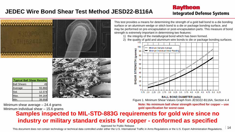
JEDEC Wire Bond Shear Test Method JESD22-B116A
This test provides a means for determining the strength of a gold ball bond to a die bonding
surface or an aluminum wedge or stitch bond to a die or package bonding surface, and
may be performed on pre-encapsulation or post-encapsulation parts. This measure of bond
strength is extremely important in determining two features:
1) the integrity of the metallurgical bond which has been formed.
2) the quality of gold and aluminum wire bonds to die or package bonding surfaces.
Typical Ball Shear Results
Ball Shears 49
Average 55.860
Std. 12.374
Max. 94.164
Min. 39.958
Note: No minimum ball shear strength specified for copper – use
gold specification for worst caseMinimum shear average – 24.4 grams
Minimum individual shear – 15.6 grams
Samples inspected to MIL-STD-883G requirements for gold wire since no
industry or military standard exists for copper - conformed as specified
Figure 1. Minimum Shear Values Graph from JESD22-B116A, Section 4.4
Approved for Public Release
This document does not contain technology or technical data controlled under either the U.S. International Traffic in Arms Regulations or the U.S. Export Administration Regulations.
15
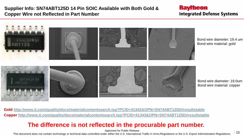
Supplier Info: SN74ABT125D 14 Pin SOIC Available with Both Gold &
Copper Wire not Reflected in Part Number
Bond wire diameter: 19.4 um
Bond wire material: gold
Gold http://www.ti.com/quality/docs/materialcontentsearch.tsp?PCID=41342&OPN=SN74ABT125D#resultstable
Copper http://www.ti.com/quality/docs/materialcontentsearch.tsp?PCID=41343&OPN=SN74ABT125D#resultstable
Bond wire diameter: 19.0um
Bond wire material: copper
The difference is not reflected in the procurable part number.Approved for Public Release
This document does not contain technology or technical data controlled under either the U.S. International Traffic in Arms Regulations or the U.S. Export Administration Regulations.
16
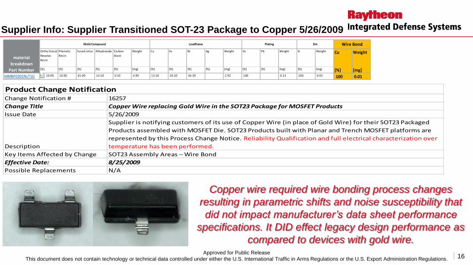
Supplier Info: Supplier Transitioned SOT-23 Package to Copper 5/26/2009
Product Change NotificationChange Notification # 16257
Change Title Copper Wire replacing Gold Wire in the SOT23 Package for MOSFET Products
Issue Date 5/26/2009
Description
Supplier is notifying customers of its use of Copper Wire (in place of Gold Wire) for their SOT23 Packaged
Products assembled with MOSFET Die. SOT23 Products built with Planar and Trench MOSFET platforms are
represented by this Process Change Notice. Reliability Qualification and full electrical characterization over
temperature has been performed.
Key Items Affected by Change SOT23 Assembly Areas – Wire Bond
Effective Date: 8/25/2009
Possible Replacements N/A
Ortho Cresol
Novolac
Resin
Phenolic
Resin
Fused silica AlHydroxide Carbon
black
Weight Cu Fe Ni Ag Weight Sn Pb Weight Si Weight Cu Weight
[%] [%] [%] [%] [%] [mg] [%] [%] [%] [%] [mg] [%] [%] [mg] [%] [mg] [%] [mg]
MMBF0201NLT1G 10.00 10.00 65.00 14.50 0.50 4.90 13.50 50.20 36.30 2.92 100 0.14 100 0.05 100 0.01
Wire Bond
material
breakdown
Part Number
Mold Compound Leadframe Plating Die
Copper wire required wire bonding process changes
resulting in parametric shifts and noise susceptibility that
did not impact manufacturer’s data sheet performance
specifications. It DID effect legacy design performance as
compared to devices with gold wire.Approved for Public Release
This document does not contain technology or technical data controlled under either the U.S. International Traffic in Arms Regulations or the U.S. Export Administration Regulations.
17
Conclusions Over 40 DPA’s (>240 parts) performed on commercial grade plastic encapsulated semiconductors & suppliers
without any failures relating to bond integrity, ball shear or bond inspection conditioned as follows:a) 24 hours at 125 +5 / -0 °C, per J-STD-020, Section 5.4
b) 168 hours of 85 °C/85% RH, per J-STD-020, Section 5.5
c) 100 cycles -55 °C / +125 °C 10 minute dwell time, per Condition B, JEDEC JESD22-A104
d) 3 cycles of SMT solder reflow per paragraph 5.6 and Table 5-2 of J-STD-020
No official qualification procedure for copper wire – USE requirements for gold wire, per MIL-STD-883, Method 2011
Several manufacturers are transitioning from gold to copper without reflecting change in part number or ordering information
Semiconductor manufacturers are reluctant to release long term storage or life reliability test results
Moving Forward… Increase stress levels during copper bond wire conditioning
– Extended life testing
Get clarification from suppliers on which parts have copper bond wires
Consider Spec. update to Include copper wirebond pull & sheer limits
Consider additional assessment / handling measures for long term storage / use bare copper wire bonded IC’s
Approved for Public Release
This document does not contain technology or technical data controlled under either the U.S. International Traffic in Arms Regulations or the U.S. Export Administration Regulations.
18
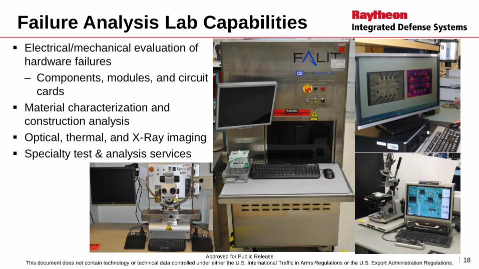
Electrical/mechanical evaluation of
hardware failures
– Components, modules, and circuit
cards
Material characterization and
construction analysis
Optical, thermal, and X-Ray imaging
Specialty test & analysis services
Failure Analysis Lab Capabilities
Approved for Public Release
This document does not contain technology or technical data controlled under either the U.S. International Traffic in Arms Regulations or the U.S. Export Administration Regulations.
19
1. Failures on DC–DC modules following a change of wire bonding material from gold to copper Y. Belfort ⁎, J.-M. Caignard, S. Keller, J.-
P. Guerveno Failure Analysis Laboratory and Technology Validation, MBDA, Le Plessis Robinson, France Microelectronics Reliability
55 (2015) 2003–2006
2. Growth behavior of Cu/Al intermetallic compounds and cracks in copper ball bonds during isothermal aging
C.J. Hang a,b,*, C.Q. Wang a, M. Mayer b, Y.H. Tian a, Y. Zhou b, H.H. Wang c
a State Key Laboratory of Advanced Welding Production Technology, Harbin Institute of Technology, Harbin 150001, China
b Centre for Advanced Materials Joining, University of Waterloo, Waterloo, Ontario, Canada N2L 3G1
c Nantong Fujistu Microelectronics Co. Ltd., Jiangsu 226001, China
Microelectronics Reliability 48 (2008) 416–424
3. Moisture/Reflow Sensitivity Classification for Nonhermetic Surface Mount Devices. Joint Industry Standard, J-STD-020E, January 2015
4. Bond reliability under humid environment for coated copper wire and bare copper wire Tomohiro Uno *
Advanced Materials & Technical Research Laboratories, Nippon Steel Corporation, 20-1 Shintomi, Futtsu-city, Chiba 293-8511, Japan
Microelectronics Reliability 51 (2011) 148–156
5. Body of Knowledge (BOK) for Copper Wire Bonds E. Rutkowski 1 and M. J. Sampson
1 ARES Technical Services Corporation,
2 NASA Goddard Space Flight Center
NASA Goddard Space Flight Center; Greenbelt, MD United States Jan 01, 2015 Document ID:20150023424
References
Approved for Public Release
This document does not contain technology or technical data controlled under either the U.S. International Traffic in Arms Regulations or the U.S. Export Administration Regulations.
20
AbstractFor years semiconductor manufacturers have used gold wire to connect the semiconductor die to the lead
frames and external pins. However, rising gold prices are driving manufacturers towards less expensive
alternative materials such as copper for use in high volume commercial plastic package devices. Military
standards such as MIL- STD-883 do not have requirements for copper bond wire and therefore manufacturers
are using qualification and process monitoring developed for gold wire to qualify the copper bond wire
technology. Although copper bond wire designs are moving forward for commercial applications, there are
concerns with quality and reliability for use of copper bond wire in high reliability military electronics with long
mission life.
This presentation will review findings from the destructive physical analysis (DPA) testing performed on a
number of standard commercial plastic encapsulated microcircuits (PEMs) used on ground-based systems. This
presentation will focus on the die ball bond and lead frame crescent bond metallurgical structures, mechanical
bond strength, wire composition, and manufacturing bonding process workmanship & overall quality.
Based on the DPA findings, potential risks will be defined along with recommendations to the qualification
program of PEMs with copper bond wire for use in harsh environments and long term high reliability military
programs.
Approved for Public Release
This document does not contain technology or technical data controlled under either the U.S. International Traffic in Arms Regulations or the U.S. Export Administration Regulations.