Embed Size (px)
Citation preview

University of Twente
Department of Electrical Engineering
Chair for Telecommunication Engineering
Performance Evaluation
of Frequency Modulation
and Slope Detection
in Analog Optical Links
by
R.B. Timens
May 28, 2009
Master thesis
Executed from 01-04-2008 to 27-03-2009
Supervisor: prof.dr.ir. F.B.J. Leferink
Advisors: dr.ir. C.G.H. Roeloffzen
ir. D.A.I. Marpaung


Summary
One unsolved challenge in the application of analog optical links is the limited dynamic
range. It is desirable to have a scheme which offers low noise and high linearity. In
other words, it is required to have a scheme employing Class-B operation in analog
optical links. In a Class-B optical link all received optical power contributes to the
radio frequency (RF)-signal power. Since the noise is dependent on the average optical
power, the noise in a Class-B optical link depends on the signal power.
A good candidate for the Class-B scheme is the combination of frequency modulation
and slope detection. The scheme consists of a directly modulated laser and an inte-
grated optical filter. The directly modulated laser generates the frequency modulated
signal. The optical filter converts the signal into two intensity modulated signals. At
the receiver end, these signals are detected by a balanced photodetector. It restores
the original modulating signal.
The filter performing the slope detection consists of two-coupler rings. It is designed
in such a way, that the conversion from frequency modulation to intensity modulation
will yield two optical signals that comprise the complementary half-wave rectified ver-
sions of the original modulating signal. This half-wave rectification is the key element
for realizing the Class-B operation in analog optical links.
The report gives an overview of the filter design. Furthermore, the feasibility of
frequency modulation by the laser and the feasibility of half-wave rectification based
on optical frequency modulation are experimentally shown.
iii

iv Summary

Contents
Summary iii
List of Abbreviations and Symbols vii
1 Introduction 1
1.1 Problem Description . . . . . . . . . . . . . . . . . . . . . . . . . . . . 1
1.2 Assignment Description . . . . . . . . . . . . . . . . . . . . . . . . . . . 4
1.3 Report Outline . . . . . . . . . . . . . . . . . . . . . . . . . . . . . . . 4
2 General Analog Optical Link Performance 7
2.1 AOL Scheme . . . . . . . . . . . . . . . . . . . . . . . . . . . . . . . . 7
2.2 Link Gain . . . . . . . . . . . . . . . . . . . . . . . . . . . . . . . . . . 8
2.3 Noise . . . . . . . . . . . . . . . . . . . . . . . . . . . . . . . . . . . . . 8
2.4 Distortion . . . . . . . . . . . . . . . . . . . . . . . . . . . . . . . . . . 10
2.5 Spurious Free Dynamic Range (SFDR) . . . . . . . . . . . . . . . . . . 12
2.6 Numerical Example . . . . . . . . . . . . . . . . . . . . . . . . . . . . . 14
3 Ideal Class-B AOL 17
3.1 Principle of Class-B in AOL . . . . . . . . . . . . . . . . . . . . . . . . 17
3.2 Noise . . . . . . . . . . . . . . . . . . . . . . . . . . . . . . . . . . . . . 17
3.3 Distortion . . . . . . . . . . . . . . . . . . . . . . . . . . . . . . . . . . 20
3.4 Dynamic Range . . . . . . . . . . . . . . . . . . . . . . . . . . . . . . . 20
4 Frequency Modulation-Slope Detection Analog Optical Link 23
4.1 Frequency Modulation-Slope Detection Scheme . . . . . . . . . . . . . 23
5 Filter Design and Simulation 25
5.1 Design Requirements . . . . . . . . . . . . . . . . . . . . . . . . . . . . 25
5.2 Digital Filter Design Approach . . . . . . . . . . . . . . . . . . . . . . 26
5.3 Available Components for Design . . . . . . . . . . . . . . . . . . . . . 27
5.3.1 Directional Coupler . . . . . . . . . . . . . . . . . . . . . . . . . 28
5.3.2 Mach-Zehnder Interferometer . . . . . . . . . . . . . . . . . . . 28
v

vi Contents
5.3.3 Ring Resonator . . . . . . . . . . . . . . . . . . . . . . . . . . . 30
5.4 Slope Detector Design . . . . . . . . . . . . . . . . . . . . . . . . . . . 33
5.4.1 DC Power Divider and Two MZIs . . . . . . . . . . . . . . . . . 33
5.4.2 DC Power Divider and Two Ring-Resonators . . . . . . . . . . . 35
5.4.3 Three Ring-Resonators . . . . . . . . . . . . . . . . . . . . . . . 37
5.4.4 Five Ring-Resonators . . . . . . . . . . . . . . . . . . . . . . . . 39
6 Measurements 43
6.1 Semiconductor Laser Diode P-I Curve . . . . . . . . . . . . . . . . . . . 43
6.1.1 Measurement Setup . . . . . . . . . . . . . . . . . . . . . . . . . 43
6.1.2 Measurement Results . . . . . . . . . . . . . . . . . . . . . . . . 44
6.2 Temperature and Current Dependences of SLD Wavelength . . . . . . . 46
6.2.1 Measurement Setup . . . . . . . . . . . . . . . . . . . . . . . . . 46
6.2.2 Measurement Results . . . . . . . . . . . . . . . . . . . . . . . . 46
6.3 DWDM Filter Transfer and SLD FM Response . . . . . . . . . . . . . 48
6.3.1 Measurement Setup . . . . . . . . . . . . . . . . . . . . . . . . . 48
6.3.2 Measurement Results . . . . . . . . . . . . . . . . . . . . . . . . 50
7 Conclusion and Recommendations 63
A SFDR, OIP and Noise Level 67
B Tables 69

List of Abbreviations and Symbols
Abbreviations
AOL analog optical link
BMD balanced modulation and detection
BPD balanced photodetector
CW continuous wave
DC directional coupler
DR dynamic range
DWDM dense wavelength division multiplexing
EAM electroabsorption modulator
EMI electromagnetic interference
FIR finite impulse response
FM frequency modulation
FSR free spectral range
HWR half-wave rectification
IM intensity modulation
IMDD intensity modulation direct detection
MZI Mach-Zehnder interferometer
MZM Mach-Zehnder modulator
NA network analyzer
NF noise figure
vii

viii List of Abbreviations and Symbols
OIP output intercept point
OSA optical spectrum analyzer
RF radio frequency
RIN relative intensity noise
RMS root mean square
SDR signal-to-distortion ratio
SFDR spurious free dynamic range
SLD semiconductor laser diode
SNR signal-to-noise ratio
VOA variable optical attenuator
Symbols
A amplitude
Ai amplitude
ai power series coefficient
BW bandwidth in dB
bw bandwidth in Hz
c speed of light
∆f maximum frequency deviation
∆LMZI relative length difference MZI branches
∆m maximum RF-current
DR2 second-order dynamic range
DR3 third-order dynamic range
fc carrier frequency
FSRMZI MZI free spectral range
FSRring ring free spectral range
ix
Glink link gain
Glink,CB link gain Class-B optical link
Glink,IMDD link gain IMDD optical link
Il laser bias current
il laser RF-current amplitude
Iph detected photocurrent
It laser threshold current
κDC DC power coupling coefficient
κMZI,1 MZI power coupling coefficient 1
κMZI,2 MZI power coupling coefficient 2
κring,1 ring power coupling coefficient 1
κring,2 ring power coupling coefficient 2
LMZI common path length MZI branches
lring ring round trip loss
LU unit length
n refractive index
Nout output noise power
OIPn power level n-th-order output intercept point
OIP2 power level second-order output intercept point
OIP3 power level third-order output intercept point
ΦDC transfer matrix DC
PF fundamental power
PIM2 second-order intermodulation power
PIM3 third-order intermodulation power
Pin RF-input power

x List of Abbreviations and Symbols
pmax maximum magnitude of fundamental
pmin minimum magnitude of fundamental
ΦMZI transfer matrix MZI
φMZI MZI phase
Pn,total total noise power
Pop optical power
Pop,CB optical power per branch in Class-B optical link
Pop,IMDD optical power IMDD optical link
Pout RF-output power
PRIN RIN power
φring ring round trip phase
Φring transfer matrix ring
Pshot shot noise power
Ptherm thermal noise power
Rin input resistance
RIN laser laser RIN power spectral density
Rload load resistance
Rpd photodetector responsivity
Rring ring radius ring resonator
SFDRn n-th-order intermodulation free spurious free dynamic range
SFDR2 second-order intermodulation free spurious free dynamic range
SFDR3 third-order intermodulation free spurious free dynamic range
sl laser slope efficiency
T absolute temperature
t time

xi
TU unit delay
ω angular frequency
ωi angular frequency
x (t) input function of time t
y(t) output function of time t

xii List of Abbreviations and Symbols

Chapter 1
Introduction
1.1 Problem Description
Analog optical links (AOLs) are used in a wide variety of applications for RF and
microwave signals distribution. In many applications, such as antenna beam forming
and phased array systems, the links are required to convey signals over a large span
of power levels, posing stringent requirements on their signal-to-noise ratio (SNR) and
linearity [1]. Noise limits the minimum detectable RF-signal power while distortion
limits the maximum RF-signal power, resulting in a limited dynamic range (DR).
Therefore, it is desired to have a scheme which offers low noise and is sufficiently
linear. Several approaches have been done to obtain this scheme by using the simple
concept of direct detecting an intensity modulated signal or intensity modulation direct
detection (IMDD). The non-physical ideal response for intensity modulation (IM) is
given in Figure 1.1. Note that negative optical power does not exist. In this figure
the modulation signal is a current or a voltage, depending on the implementation.
The shown response is ideal, since there is no optical power when the signal is zero.
Moreover, the curve is linear. These two properties are essential for obtaining high
DR as will become clear later on. As far we know, however, the ideal response is
never approached to a satisfying degree. We can find the reason for this in [3], where
it is argued that the conventional IMDD links do not meet the two aforementioned
requirements.
For example, consider the case of direct modulation of a semiconductor laser diode
(SLD), and the two cases of external modulation of a continuous wave (CW) laser by
a Mach-Zehnder modulator (MZM) and an electroabsorption modulator (EAM). The
corresponding responses are shown in Figure 1.2. For the purpose of linear operation,
the laser and modulators are biased as indicated by the dot, resulting in large average
optical power. Detection of large optical power will result in large noise power, since the
dominant noise sources, RIN and shot noise, are increasing with the optical power [5].
This, in turn, will limit the link DR [2]. For the purpose of operation at low average
1
2 Chapter 1. Introduction
Figure 1.1: Non-physical ideal response for IM
optical power, the laser and modulators are biased as indicated by the square, resulting
in large nonlinearities. This, in turn, will also limit the link DR [2].
Figure 1.2: Biasing of an SLD (a), an EAM (b) and an MZM (c)
Figure 1.3 illustrates the limitations in DR for the case of direct modulation in more
detail. As shown in Figure 1.3 (a) low biasing results in a low average optical power
and therefore in a low noise power, but also in clipping of large signals. Higher biasing
avoids the signal clipping, but also results in a larger average optical power and thus a
larger noise power. This larger noise power dominates over small signals, as is shown
in Figure 1.3 (b).
In order to decrease the large noise power without increasing the nonlinearities,
one could attempt to use a balanced transmitter in which two SLDs are biased around
threshold. In this way, one can theoretically obtain the ideal response of Figure 1.1.
However, as is shown in [6], biasing a laser near threshold point leads to nonlinearities
in the laser and relative intensity noise (RIN) enhancement, which limits the achievable
DR of this so called balanced modulation and detection (BMD) link.
The work of [6] uses the BMD scheme in an attempt to obtain a link in which all
received optical power linearly contributes to the RF-signal power. In other words, it
is tried to obtain a link which operates without a dc-bias. The ideal case of such a

1.1. Problem Description 3
Figure 1.3: Biasing of an intensity modulated SLD: low biasing results in clipping of large
signals (a), but high biasing results in a large optical power and therefore a
large noise power (b).
link operation is known as Class-B operation [3]. To realize the Class-B optical link,
several methods have been proposed [3], [6]. But, all these attempts have resulted in
limited improvement due to an increase in nonlinearities or noise [3].
In this report, we propose a scheme to realize the Class-B optical link. We use an
integrated optical ring-resonator based slope detector (or frequency discriminator) to
realize the ideal response in Figure 1.1. The scheme in Figure 1.4 shows the frequency
modulation-slope detection analog optical link (AOL), in which the electrical parts
and optical parts are explicitely indicated. It is widely known that a direct modulated
Figure 1.4: The frequency modulation (FM)-slope detection AOL
SLD exhibits variation in its intensity as well as in its frequency. This FM is known
as the frequency chirping. In this scheme, the frequency chirp is used to carry the
information. By means of optical filtering, the FM is subsequently converted to IM.

4 Chapter 1. Introduction
The filter responses are chosen such that the resulting intensity modulated signals are
complementary half-wave rectified versions of the modulating RF-signal. These optical
signals are detected by a balanced photodetector (BPD) in the receiving side. The
desired filter responses are shown in Figure 1.5 and subtraction of the two individual
responses results in a straight line, which is required for slope detection. The corre-
Figure 1.5: Optical filter responses
sponding half-wave rectification (HWR) suppresses the dc optical carrier which is the
main contributor for the total RF noise power in AOLs. The reduction in noise power
by this optical carrier suppression will lead to DR enhancement.
1.2 Assignment Description
The main goal of the project is to design the integrated optical slope detector and
to demonstrate the FM-slope detection scheme. The following tasks are carried out
during the project:
1. Investigate the feasibility of optical FM in SLDs.
2. Design of the optical filter according to the desired response of Figure 1.5.
3. Investigate the feasibility of HWR based on optical FM.
1.3 Report Outline
In Chapter 2 the general AOL scheme and its performance are discussed. In Chapter 3
the characteristics of the ideal Class-B link are discussed. This discussion evaluates
the ideal Class-B optical link performance using the conventional IMDD link as a
benchmark. In Chapter 4 the FM-slope detection AOL is described and attention will
be paid on how Class-B operation is obtained using this link. This discussion is the

1.3. Report Outline 5
starting point for the slope detector design on which Chapter 5 is devoted. For this
design, simulations in LabVIEW 8.5 are carried out. Since it is not possible to fabricate
the filter in the project, existing DWDM-filters are used for the measurements. In this
way, the concept or principal can be verified. The results of these measurements are
discussed in Chapter 6. The report closes with the conclusion in Chapter 7.

6 Chapter 1. Introduction

Chapter 2
General Analog Optical Link
Performance
In this chapter the analog optical link (AOL) is introduced. First, the general scheme
and its advantages are discussed. Next, the discussion continues with the problems
related to AOLs. In this discussion, the terms link gain, relative intensity noise (RIN),
shot noise, thermal noise, harmonic distortion, intermodulation distortion and spurious
free dynamic range (SFDR) are defined.
2.1 AOL Scheme
AOLs are used in a wide variety of applications for RF and microwave signals distri-
bution, due to the following advantages over coaxial cables:
• low propagation loss
• wide bandwidth
• immunity for electromagnetic interference (EMI)
• small size
• light weight.
The general scheme of an AOL is shown in Figure 2.1. It consists of an electro-
to-optical converter (modulation device) and an optical-to-electrical converter (optical
detector). At the input of the link, the RF-signal is converted to the optical domain
by the modulation device. At the output of the link, the signal is back-converted to
the RF domain by the optical detector.
The conversion efficiency in the modulation device is called slope efficiency. De-
pending on the implementation, it is defined as the ratio of the variation in optical
power over the corresponding variation in current (in W/A) or voltage (in W/V). The
7

8 Chapter 2. General Analog Optical Link Performance
Figure 2.1: General AOL-scheme
conversion efficiency in the optical detector is called responsivity. It is defined as the
ratio of the variation in current over the corresponding variation in detected optical
power (in A/W). However, the conversions are inefficient. Practical values for the SLD
slope efficiency are between 0.015 and 0.3 W/A, and for the photodiode responsivity
are between 0.7 and 1.0 A/W [5]. Furthermore, the conversions are accompanied by
noise and distortion [5]. This will, in turn, degrade the performance of an AOL.
2.2 Link Gain
The link gain, Glink, can be defined as the ratio of RF-output and -input powers as
follows:
Glink =Pout
Pin
(2.1a)
or, in decibels it can be expressed as:
Glink (dB) = Pout (dBm)− Pin (dBm) (2.1b)
In Equation (2.1) Pin denotes the RF-input power and Pout the RF-output power of
the link. Because of the inefficient conversions in the modulation device and optical
detector, the output power of the AOL is smaller than the input power. This results
in a link gain value which is smaller than 1. In other words, the optical link can be
considered as a lossy component.
2.3 Noise
Three noise sources are contributing to the link noise. The first one is relative intensity
noise (RIN) and finds its origin in the laser. Spontaneous emission is needed to initialize
the laser mechanism (stimulated emission) in an SLD. However, it is still present when
an SLD is in lasing mode and therefore contributes an incoherent part to the laser
output field. Especially around threshold current, the spontaneous emitted power
relative to the stimulated emitted power is large.

2.3. Noise 9
The laser RIN-power spectral density, RIN laser, is defined as the variance of the
spontaneous emitted power relative to the square of the total average optical power as
shown in Equation (2.2) [5]. The laser RIN-power spectral density is unitless.
RIN laser =〈(Pop − 〈Pop〉)2〉
〈Pop〉2=〈p2
RIN〉〈Pop〉2
(2.2)
The spontaneous emitted power or incoherent part of the output field gives rise
to instantaneous intensity fluctuations, and detection of these fluctuations results in
intensity noise. The associated RIN power per unit electrical bandwidth, PRIN, is
described as:
PRIN (W/Hz) = RIN laser · 〈Iph〉2 ·Rload (2.3)
In Equation (2.3), RIN laser denotes the laser RIN-power spectral density (in 1/Hz), Iph
denotes the detected photocurrent (in A) and Rload denotes the load resistance (in Ω).
Iph depends on the photodetector responsivity, Rpd (in A/W), and optical power, Pop
(in W), as follows:
Iph (A) = Rpd · Pop (2.4)
The second noise source is the shot noise which finds its origin in the generation
of photocurrents arising from a series of independent random events. Mainly, it is
driven by the random arrival of photons on the photodetector [5]. This results in an
instantaneous current, which is not constant, although the average current is constant.
The shot noise power, Pshot, is described as [5]:
Pshot (W/Hz) = 2 · e · 〈Iph〉 ·Rload (2.5)
The last noise source is the thermal noise and also finds its origin in the detector.
The thermal noise is the result of thermal induced random movements of carriers
giving rise to a nonzero instantaneous current, with zero average. Assuming impedance
matching, the transferred thermal noise power is described as:
Ptherm (W/Hz) = k · T (2.6)
In Equation (2.6), k denotes Boltzmann’s constant (in J/K) and T denotes the absolute
temperature (in K). Unlike the RIN and shot noise power, the thermal noise power is
independent of the optical power.
The total noise, Pn,total, in the AOL is the sum of Equations (2.3), (2.5) and (2.6):
Pn,total (W/Hz) = PRIN + Pshot + Ptherm (2.7a)
or, in decibels it can be expressed as:
Pn,total (dBm/Hz) = 10 log10
(PRIN + Pshot + Ptherm
0.001
)(2.7b)

10 Chapter 2. General Analog Optical Link Performance
2.4 Distortion
The nonlinearities in the modulation device and the optical detector result in distor-
tion. To evaluate the nonlinear distortion, the transfer characteristic is mathematically
expressed by writing the output y(t) as a power series of the input x (t):
y(t) = a1x(t) + a2x2(t) + a3x
3(t) + . . . (2.8)
It is assumed that only the second- and third-order nonlinearities are of concern and
as a result the fourth and higher order terms of Equation (2.8) are ignored. Consider
a single sinusoidal wave at the input:
x(t) = A cos(ωt) (2.9)
Harmonic distortion spectral components will then arise at the output at angular fre-
quencies 0, ω, 2ω and 3ω. Next, consider a two tone signal with the closely spaced
tones ω1 and ω2 at the input:
x(t) = A1 cos(ω1t) + A2 cos(ω2t) (2.10)
Now not only harmonic distortion, but also intermodulation distortion arises with
spectral components at the sum and difference frequencies of the two tone signal, i.e.
at ω1 ± ω2, 2ω1 ± ω2 and ω1 ± 2ω2. Table 2.1 gives an overview of the two types of
distortion up to the third-order, with corresponding frequency and amplitude.
Table 2.1: Overview distortion components
Order Angular frequency Amplitude
Single tone Dc 0 12a2A
Fundamental ω a1A+ 34a3A
3
Second-order 2ω 12a2A
2
Third-order 3ω 14a3A
3
Two tone Dc 0 12a2A
21 + 1
2a2A
22
Fundamental ω1, ω2 a1A1 + 32a3A1A
22 + 3
4a3A
31,
a1A2 + 32a3A
21A2 + 3
4a3A
32
Second-order ω1 + ω2, ω1 − ω2 a2A1A2, a2A1A2
2ω1, 2ω212a2A
21,
12a2A
22
Third-order 2ω1 + ω2, 2ω1 − ω234a3A
21A2,
34a3A
21A2
ω1 + 2ω2, ω1 − 2ω234a3A1A
22,
34a3A1A
22
3ω1, 3ω214a3A
31,
14a3A
32
In the remaining part of the discussion, we consider only the frequencies within one
octave of the signal frequencies. Therefore, the frequencies higher than 2ω1 and 2ω2
are ignored.

2.4. Distortion 11
Figure 2.2(a) gives an example of a two tone signal at the input of a noisy, nonlinear
device and Figure 2.2(b) shows the output signal of that device. Since the coefficient
a2 appears in the amplitude of the DC-component (see Table 2.1), the average of the
output signal is larger than zero. Furthermore, the contribution of the coefficient a3 to
the amplitude of the fundamental results in the signal amplitude reduction. Moreover,
the output signal is noisy. The spectra of the signals in Figure 2.2 are shown in
0 , 0 0 , 2 0 , 4 0 , 6 0 , 8 1 , 0- 1 , 0- 0 , 8- 0 , 6- 0 , 4- 0 , 20 , 00 , 20 , 40 , 60 , 81 , 0
Norm
alized
Amplit
ude
N o r m a l i z e d T i m e(a)
0 , 0 0 , 2 0 , 4 0 , 6 0 , 8 1 , 0- 1 , 0- 0 , 8- 0 , 6- 0 , 4- 0 , 20 , 00 , 20 , 40 , 60 , 81 , 0
Norm
alized
Amplit
ude
N o r m a l i z e d T i m e(b)
Figure 2.2: Input signal (a) and noisy, distorted output signal (b).
Figure 2.3 in which the frequency components are indicated. The same observations
can be made as we did in Figure 2.2. The spectrum of the output signal has a large DC
component. Furthermore, the spectrum plots show that the relative power of the two
signal tones ω1 and ω2 at the output is lower than at the input. This corresponds to
the observed signal amplitude reduction. Moreover, the spectrum of the output signal
is noisy. Besides, from the output signal spectrum plot can be derived the difference in
consequences of the nonlinearities for narrow- and broadband signals. For narrowband
signals, only the third order distortion is important. In terms of Figure 2.2(b) the
frequencies 2ω1 − ω2 and 2ω2 − ω1 are important. For broadband signals the second
order distortion also comes into play. In terms of Figure 2.2(b) the frequencies ω1 +ω2
and ω2 − ω1 also play an important role.
A measure of distortion is the intercept point at which the fundamental power and
the intermodulation power are equal [5]. In Figure 2.4 the output powers versus the
input (signal) power is shown, both on log scales. The power at which the fundamental
and one of the distortion curves intersect is called the intercept point. Equations (2.11a)
and (2.11b) describe the conditions for the second- and third-order intercept points,
respectively. In these equations, PF denotes the fundamental power, PIM2 denotes the
second-order intermodulation power and PIM3 denotes the third-order intermodulation
power.
PF = PIM2 (2.11a)

12 Chapter 2. General Analog Optical Link Performance
0 , 0 0 , 5 1 , 0 1 , 5 2 , 0 2 , 51 0 - 1 11 0 - 1 01 0 - 91 0 - 81 0 - 71 0 - 61 0 - 51 0 - 41 0 - 3
ω2
N o r m a l i z e d F r e q u e n c y
Relat
ive Po
wer ω
1
(a)
0 , 0 0 , 5 1 , 0 1 , 5 2 , 0 2 , 51 0 - 1 11 0 - 1 01 0 - 91 0 - 81 0 - 71 0 - 61 0 - 51 0 - 41 0 - 3
D Cω
2 − ω
1 2ω1 − ω
22ω
2 − ω
1
3ω1 − ω
23ω
2 − ω
1
ω1 + ω
2
N o r m a l i z e d F r e q u e n c y
Relat
ive Po
wer
ω2
ω1
(b)
Figure 2.3: Spectrum of the input signal (a) and output signal (b) of Figure 2.2.
PF = PIM3 (2.11b)
When doing distortion measurements, the fundamental, the second-order and the third-
order powers at the output of the AOL are measured. Therefore, it is convenient to
use the output as reference for the intercept points. As a result, the second-order and
the third-order intercept points are referred to as the second-order and the third-order
output intercept points (OIPs), respectively. Since every system has its own second-
and third-order OIPs, these points are useful measures for the system performance.
The higher the intercept points, the lower is the distortion for a given fundamental (or
desired output signal) power. To avoid serious distortion, practical systems are always
operated below these points.
2.5 Spurious Free Dynamic Range (SFDR)
In order to compare the performance of different AOLs, another measure is defined.
This measure is the spurious free dynamic range (SFDR) which accounts for the noise
power as well as the intermodulation power. Let the minimum power that a link
can convey, pmin, be the fundamental power corresponding to the intersection of the
fundamental power and the noise power. Furthermore, let the maximum power, pmax
that a link can convey without any measurable distortion, be the fundamental power
corresponding to the intersection of the distortion power and the noise power [5]. The
ratio between this pmax and pmin is the SFDR. It is indicated in Figure 2.5 for the
second-order and third-order intermodulation products, IM2 and IM3, as SFDR2 and
SFDR3, respectively. Because of symmetry, the SFDR can be drawn along the input
power axis as well as along the output power axis. From this notion, the SFDR can
also be defined as the SNR corresponding to the intersection of distortion and noise
powers.

2.5. Spurious Free Dynamic Range (SFDR) 13
I M 2
I n p u t P o w e r ( d B m )
O u t p u t P o w e r ( d B m )
F u n d a m e n t a l
I M 3
N o i s e ( 1 H z )
O I P 3
O I P 2
Figure 2.4: Plot of the fundamental output power, the second-order and third-order in-
termodulation output powers as a function of the input power for defining the
second- and third-order OIPs.
It is convenient to express the SFDR in an 1-Hz noise bandwidth. By using the
appropriate scaling law, the 1-Hz number can be scaled to any desired bandwidth. The
general scaling law is given by [5] as:
SFDRn [bw ] = SFDRn [1 Hz] · (bw)−n−1n (2.12a)
or in dB:
SFDRn [bw ] = SFDRn [1 Hz]− (n− 1)
nBW (2.12b)
An illustration of the scaling laws is shown in Figure 2.6. In Figure 2.6(a) the
increase in SFDR2 for 40 dB decrease in noise power (1 Hz) is shown. In the initial
case the SFDR2 is 70 dB (∆1). After decreasing the noise level, the SFDR2 becomes
90 dB (∆2). This corresponds to a change of 20 dB in SFDR2 (∆SFDR2). Therefore,
SFDR2 scales as −12BW with BW the bandwidth in dB and as (bw)−
12 with bw the
linear bandwidth. Note that a 40 dB increase in the noise bandwidth has the same
result as increasing the noise power by 40 dB in the original noise bandwidth. A similar
approach is followed for the SFDR3 as shown in Figure 2.6(b). A 40 dB decrease in
noise power corresponds to 26.7 dB increase in SFDR3. As a result, SFDR3 scales as
−23BW with BW the bandwidth in dB and as (bw)−
23 with bw the linear bandwidth.
Suppose the SFDR2 (in dB) for unity bandwidth is known and it is desired to
convert this to a bandwidth of 1.0 GHz. First, one has to calculate the ratio of these

14 Chapter 2. General Analog Optical Link Performance
I M 2
P i n ( d B m )
P o u t ( d B m )
F u n d a m e n t a l
N o i s e ( 1 H z )
S F D R 2
(a)
P i n ( d B m )
P o u t ( d B m )
F u n d a m e n t a l
I M 3
N o i s e ( 1 H z )
S F D R 3
(b)
Figure 2.5: Plot of the fundamental output power, the second-order and third-order in-
termodulation output powers as a function of the input power for defining the
SFDR2 (a) and SFDR3 (b).
two bandwidths, which is 90 dB. Secondly, one has to apply the scaling law, −12BW ,
resulting in SFDR2 (1 GHz) = SFDR2 (1 Hz) − 45 dB. Taking another example for
SFDR3 of scaling from unity bandwidth to 1.0 GHz bandwidth, one obtains SFDR3 (1
GHz) = SFDR3 (1 Hz) − 60 dB.
The above discussed scaling law in Equation (2.12) appears also in the relation
between SFDR and OIP. This relation is mathematically expressed in Equation (2.13).
In Appendix A, the relation between SFDR and OIP is discussed in more detail.
SFDRn [dB] =(n− 1)
n
(OIPn [dBm]−Nout [dBm]
)(2.13)
2.6 Numerical Example
The concept of SFDR is illustrated by a numerical example. We consider an IMDD-
link of which the link parameters are listed in Table 2.2. In this example, four different
situations are calculated by changing three link parameters. The situations and corre-
sponding calculated results are listed in Table 2.3. In the first situation, all the link
parameters are set to their initial values. In the other situations, only one parame-
ter differs from its initial value. The change in parameter settings affects the noise
level, resulting in other SFDR values. In other words, this example illustrates three
parameters affecting the SFDR.

2.6. Numerical Example 15
∆S F D R 2 = ∆2 - ∆1 = 2 0 d B∆S F D R 2 / ∆n = 1 / 2
∆2= 9 0 d B
∆n = 4 0 d B
N o i s e 1 ( 1 H z )
I M 2
P i n ( d B m )
P o u t ( d B m )
F
N o i s e2 ( 1 H z )
∆1 = 7 0 d B
(a)
∆1 = 8 3 1 / 3 d B
∆S F D R 3 = ∆2 - ∆1 = 2 6 2 / 3 d B∆S F D R 3 / ∆n = 2 / 3
∆2= 1 1 0 d B
∆n = 4 0 d B
N o i s e 1 ( 1 H z )
I M 3
P i n ( d B m )
P o u t ( d B m )
F
N o i s e2 ( 1 H z )
(b)
Figure 2.6: Plot of SFDR2 (a) and SFDR3 (b) for two different noise power levels.
Table 2.2: The simulation parameters for numerical example
Parameter Symbol Value Units
laser slope efficiency sl 0.3 W/A
photodetector responsivity Rpd 0.8 A/W
laser RIN power spectral density RIN laser -155 dB/Hz
load resistance Rload 50 Ω
input resistance Rin 50 Ω
absolute temperature T 293 K
noise bandwidth bw 10 MHz
laser threshold current It 15 mA
laser bias current Il 75 mA
power level second-order output intercept point OIP2 43.6 dBm
power level third-order output intercept point OIP3 20.6 dBm
link gain Glink -12.4 dB
Table 2.3: The four simulated situations in the numerical example
Situation Changed New Value Noise level SFDR2 SFDR3
Parameter (dBm) (dB) (dB)
1 - - -49.98 46.8 47.1
2 RIN laser -120 dB/Hz -15.05 29.3 23.8
3 Il 100 mA -46.97 45.3 45.0
4 bw 100 MHz -39.98 41.8 40.4

16 Chapter 2. General Analog Optical Link Performance

Chapter 3
Ideal Class-B AOL
In this chapter the characteristics of the ideal Class-B optical link are discussed. This
discussion evaluates the ideal Class-B optical link performance using the conventional
IMDD link as a benchmark.
3.1 Principle of Class-B in AOL
As discussed in the previous chapter, there is a demanding need for links in which
all received optical power contributes to the RF-signal power. Moreover, a quadratic
relation between optical power and RF-signal power is required. In other words, there
is a demanding need for Class-B operation in AOLs or links having the ideal response
of Figure 1.1.
In an ideal Class-B optical link, the dc-bias link operation is avoided by linearly
converting the modulating RF-signal into a pair of complementary half-wave rectified
optical signals [3]. An illustration is shown in Figure 3.1(a) for a sinusoidal input
signal. Due to this half-wave rectification (HWR), optical power is transmitted only
in the presence of an RF-signal. As a result, the optical power becomes a function of
the RF-signal, as is shown for both signal parts. In Figure 3.2 the ideal response of
the HWR is shown. In order to restore the original RF-signal, both complementary
half-wave rectified optical signals need to be detected. Furthermore, the detected
complementary signals have to be subtracted from each other. These two processes
can be carried out by a differential detection scheme. In other words, a modulation
device employing HWR and a differential detector are needed to implement a Class-B
optical link, as is shown in Figure 3.1(b).
3.2 Noise
As is discussed in section 2.3, shot noise and RIN depend linearly and quadratically
on optical power, respectively. Therefore, they depend on the RF-signal in a Class-B
17

18 Chapter 3. Ideal Class-B AOL
(a) (b)
Figure 3.1: Dc-bias suppression by HWR (a) and the ideal Class-B optical link (b)
Figure 3.2: Ideal response for HWR
optical link [2], [3]. To illustrate the advantage of this, the theoretical approach in [2]
is followed. In this work the Class-B optical link is constructed using a balanced pair
of directly modulated lasers as modulation device.
In order to evaluate the Class-B noise performance, a mathematically description
for the average optical power per branch is needed. We assume that both branches
have equal average optical power, such that we only need to determine the optical
power of one branch. Considering the upper branch of the scheme in Figure 3.1(b), its
optical power, Pop, is mathematically expressed as:
Pop [W] =
slil sin 2πt
Tfor 0 < t ≤ T
2
0 for T2< t ≤ T
(3.1)
In Equation (3.1), sl denotes the laser slope efficiency (in W/A), il denotes the laser
RF-current amplitude (in A), t denotes the time and T denotes the period time. The

3.2. Noise 19
average of this power, 〈Pop,CB〉, is as follows:
〈Pop,CB〉 [W] =1
2π
(∫ T2
0
slil sin2πt
Tdt+
∫ T
T2
0 dt
)=slilπ
(3.2)
By using the Equations (2.3), (2.5) and (3.2), the RIN and shot noise powers in
the upper branch can be determined. By considering the noise processes of the upper
branch to be independent of the lower branch, the total shot noise and RIN power is
two times that of the upper branch.
Furthermore, to simulate the performance of a conventional IMDD link for using it
as a benchmark, a description of its average optical power 〈Pop,IMDD〉 is needed. The
average optical power is dependent on the biasing of the laser, or the laser bias current
Il (in A), and the laser threshold current It, and is written as:
〈Pop,IMDD〉 [W] = sl · (Il − It) (3.3)
By using the Equations (2.3), (2.5) and (3.3), the RIN and shot noise powers in the
conventional IMDD link can be determined.
The noise powers (in 10 MHz effective noise bandwidth) of both links are simulated
in LabVIEW 8.5. The parameters used in the simulations are listed in Table 3.1. Using
these parameters and Equations (3.2) and (3.3), results in the same link gain for both
links, Glink,CB = Glink,IMDD = −12.40 dB.
Table 3.1: Simulation parameters for noise performance analysis of Class-B and IMDD
optical links
Parameter Symbol Value Units
laser slope efficiency sl 0.3 W/A
photodetector responsivity Rpd 0.8 A/W
laser RIN power spectral density RIN laser -155 dB/Hz
load resistance Rload 50 Ω
input resistance Rin 50 Ω
absolute temperature T 293 K
noise bandwidth bw 10 MHz
laser threshold current* It 15 mA
laser bias current** Il 75 mA
* = also bias point for lasers in Class-B optical link simulation
** = only for IMDD optical link simulation: most linear operating point
The simulation results are shown in Figure 3.3. It shows the RF-input power
independence of the noise in the IMDD optical link. The most dominant noise source

20 Chapter 3. Ideal Class-B AOL
is RIN. Furthermore, the figure shows the RF-input power dependence of the RIN and
the shot noise in the Class-B optical link. For low RF-input power, the total link noise
is equal to the thermal noise power. When the RF-input power becomes larger, the
shot noise comes into play and ultimately the RIN becomes dominant.
- 3 0 - 2 0 - 1 0 0 1 0 2 0- 1 4 0
- 1 3 0
- 1 2 0
- 1 1 0
- 1 0 0
- 9 0
- 8 0
- 7 0
Noise
powe
r (dBm
)
R F - i n p u t p o w e r ( d B m )
C l a s s - B
- 3 0 - 2 0 - 1 0 0 1 0 2 0- 1 4 0
- 1 3 0
- 1 2 0
- 1 1 0
- 1 0 0
- 9 0
- 8 0
- 7 0
( a )
I M D D
R I N S h o t n o i s e T h e r m a l n o i s e T o t a l n o i s e
Noise
powe
r (dBm
)
R F - i n p u t p o w e r ( d B m )( b )
Figure 3.3: Simulation results of an ideal Class-B (a) and an IMDD (b) optical link: Noise
power (bw = 10 MHz) versus RF-input power.
To get a better impression of these results, the SNR of both links is shown in
Figure 3.4. It is evident from this figure that the Class-B optical link gives a significant
advantage over the conventional IMDD optical link in a wide range of RF-input powers.
Notably in the small signal region, where the SNR is premium, an impressive SNR
improvement of 29 dB has been achieved.
3.3 Distortion
The distortion analysis of the Class-B optical link is beyond the scope of this report.
For an analysis based on the BMD scheme, where a balanced pair of directly modulated
lasers are used as modulation device, the reader is referred to the work of [2].
3.4 Dynamic Range
Since the RIN and the shot noise in the Class-B optical link are a function of the RF-
signal, the SFDR can not be used as performance measure. Therefore, we use another
performance measure for Class-B optical links. It is the range of RF-power which
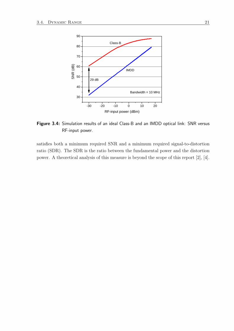
3.4. Dynamic Range 21
- 3 0 - 2 0 - 1 0 0 1 0 2 0
3 0
4 0
5 0
6 0
7 0
8 0
9 0
I M D D
C l a s s - B
SNR (
dB)
R F - i n p u t p o w e r ( d B m )
2 9 d B
B a n d w i d t h = 1 0 M H z
Figure 3.4: Simulation results of an ideal Class-B and an IMDD optical link: SNR versus
RF-input power.
satisfies both a minimum required SNR and a minimum required signal-to-distortion
ratio (SDR). The SDR is the ratio between the fundamental power and the distortion
power. A theoretical analysis of this measure is beyond the scope of this report [2], [4].

22 Chapter 3. Ideal Class-B AOL

Chapter 4
Frequency Modulation-Slope
Detection Analog Optical Link
In this chapter the frequency modulation (FM)-slope detection AOL realizing the Class-
B optical link is discussed. The FM combined with the slope detection in the FM-slope
detection AOL are employed to obtain half-wave rectification (HWR). Later on, this
chapter is used as starting point in the filter design, where the designed optical filter
has to perform the slope detection.
4.1 Frequency Modulation-Slope Detection Scheme
Laser Diode
DC bias
OpticalFilter
Balanced Detector
Transmitter Receiver
(a)
Laser Diode
DC bias
OpticalFilter
Balanced Detector
Transmitter Receiver
(b)
Figure 4.1: FM-slope detection AOL.
The proposed link consists of a directly modulated laser, an optical filter acting
as slope detector and a balanced detector, as is shown in Figure 4.1(a). To be con-
sistent with Figure 3.1(b), the SLD combined with the optical filter is indicated as
’Transmitter’, but the optical filter can also be part of the ’Receiver’, as is shown in
Figure 4.1(b). This last implementation is more practical, since a single fiber is needed
for connecting the transmitter and receiver ends.
In both schemes of Figure 4.1 the frequency chirping characteristic of an SLD is em-
ployed generating a frequency modulated optical carrier. The instantaneous frequency
23

24 Chapter 4. Frequency Modulation-Slope Detection Analog Optical Link
deviation linearly corresponds to the instantaneous amplitude of the RF-signal, as is
shown in Figure 4.2 (a) [7]. In this figure the ideal frequency response of the laser
chirp as function of the modulating RF-current is shown. The maximum RF-current
is denoted by ∆m and the maximum optical frequency deviation is denoted by ∆f .
As a result of direct modulation of the SLD, not only the frequency but also the
intensity of the carrier is modulated. Therefore, a frequency as well as an intensity
modulated optical carrier will be present at the filter input. To simplify the discussion
intensity modulation is neglected at this point.
Figure 4.2: Ideal chirp transfer (a) and ideal slope transfer (b)
The optical filter has two branch outputs of which ‘Branch 1’ linearly converts
the optical frequencies higher than fc into intensity and ‘Branch 2’ does the same for
frequencies lower than fc, as is shown in Figure 4.2 (b). In this way, FM to IM conversion
will yield two optical signals that comprise complementary half-wave rectified versions
of the original modulating RF-signal. Since the transmission is zero at the carrier
frequency, fc, for both branches, the optical power of the laser is suppressed. The
balanced detector then detects the optical signals, resulting in the total filter response
of Figure 4.2 (b).
Above, it was pointed out that the carrier at the filter input is modulated in its
frequency as well as in its intensity. In the RF-domain a similar situation occurs when
employing FM. Variations in the carrier amplitude are induced by the FM transmitter
or by variations in the signal path from transmitter to receiver. In order to reduce
the signal level changes a signal limiter is used in the FM receiver. To our knowledge
however, there are no intensity limiters in the optical domain to cancel the intensity
modulation of the laser. For now, we only assume that the frequency modulation index
is much larger than the intensity modulation index of the laser. Later on, measurements
must validate the assumption of negligible intensity modulation.

Chapter 5
Filter Design and Simulation
This chapter discusses the design of the slope detector of which the general requirements
are described in Chapter 4. The discussion starts with the design requirements. Next,
the choice of building blocks is discussed. Then, several designs are made and simulated
in LabVIEW 8.5. In this last design stage, a simple concept is improved step-by-step.
The discussion ultimately arrives at the final design.
5.1 Design Requirements
The main design constraint is to realize the ideal filter response in Figure 4.2 (b)
without having an extremely complicated structure. A complicated structure is not
only difficult to fabricate, but it also complicates the simulation. To ensure proper
HWR, the branch transfers must have an instantaneous transition from the flat to the
linear response around the carrier frequency. In Figure 5.1 three examples are shown
of improper transitions at the carrier frequency. Misalignment of the branch transfers
(case 1) leads to distortion. Besides, power leakage at the carrier frequency can occur
when the passband of the branch transfers have an overlap (case 2). Moreover, gradual
transitions (case 3) will result in distortion and power leakage at the carrier frequency.
Branch 1
Branch 2
Optical Frequency
0
1
-1
Tra
ns
mis
sio
n
Total fc f +?c ff -?c f
1
2
3
Figure 5.1: Filter transfer
Another important constraint is to make the slope detector integratable with the
25

26 Chapter 5. Filter Design and Simulation
balanced detector, resulting in a small receiver device. Therefore, it is required to have
a design based on an integrated chip. Furthermore, it is desirable to have a tunable
slope detector to compensate fabrication tolerances and for flexibility purposes. In this
way, it is taken into advance the possibility of using the same filter for different optical
FM-sources. It is assumed that the FM-index is large enough to neglect the IM-index,
so there is not accounted for the laser IM response in the design.
5.2 Digital Filter Design Approach
In [8] it is pointed out that the digital signal processing techniques are relevant to
optical filters, because they are linear, time-invariant systems that have discrete delays.
Just as is the case for digital filters, optical filters have splitters, delays and combiners
as basic elements. Therefore, the filter design is based on digital signal processing
concepts.
Digital filters are described by the Z-transform. The Z-transform is an analytical
extension of the discrete-time Fourier transform for discrete signals. Consider the
discrete-time Fourier transform of a discrete signal, x(k):
X(ω) =∞∑
k=−∞
x(k)e−jωk (5.1)
Its Z-transform is obtained by substituting z for ejω as follows:
X(z) =∞∑
k=−∞
x(k)z−k (5.2)
In the Z-transform description z−1 represents the unit delay. It is noted that a filter
having impulse response h(k) must satisfy the condition h(k) = 0 for k < 0 in order to
be causal.
The unit delay, TU, in optical filters is defined as follows:
TU =LUn
c(5.3)
In Equation (5.3) denotes n the group index, c the speed of light and LU the unit delay
or smallest path length difference. In general, the optical path lengths in an optical
filter are integer multiples of the unit delay length, resulting in a periodic frequency
response. One period of the frequency response is defined as free spectral range (FSR)
and is mathematically expressed as follows:
fFSR =1
TU
=c
LUn(5.4)

5.3. Available Components for Design 27
5.3 Available Components for Design
The slope detector must be fabricated in an optical chip, resulting in a limited number
of filter stages or number of delay elements. As a result, the ideal response can only be
approximated. Furthermore, the filter components which can be realized in an optical
chip are directional coupler (DC), ring-resonator and Mach-Zehnder interferometer
(MZI). The schematics of these components are shown in Figure 5.2. Note that the
DC is part of the MZI and the ring-resonator.
Figure 5.2: Available filter components: (a) DC, (b) MZI and (c) ring-resonator.
Figure 5.3: Z-transform schematics of (a) DC, (b) MZI and (c) ring-resonator, and trans-
fer matrix representations of (d) DC, (e) MZI and (f) ring-resonator.
It is useful to consider the transfer functions of the components. For this, the Z-
transform schematics are considered first, which are shown in Figure 5.3. In this figure
X1 and X2 represent the input field amplitudes and Y1 and Y2 represent the output field
amplitudes. Furthermore, the through- and cross-port transmissions are respectively
designated by c and −js. Those are related to the power coupling coefficient κ as

28 Chapter 5. Filter Design and Simulation
follows:
c =√
1− κ (5.5a)
− js = −j√κ (5.5b)
Note that the sum of the squares of the transmission is 1 or:
c2 + (−js)2 = (√
1− κ)2 + (−j√κ)2 = 1 (5.6)
In other words, the sum of the transmission powers is equal to 1, thereby fulfilling the
power conservation condition.
5.3.1 Directional Coupler
The Z-transform of the directional coupler (DC) is shown in Figure 5.3 (a). Using this
Z-transform the 2 × 2 transfer matrix, ΦDC, can be derived. This matrix describes
the relations between the input and output fields for the DC as in Equation 5.7. The
matrix is shown in Figure 5.3 (d).[Y1
Y2
]=
[c −js−js c
] [X1
X2
]
= ΦDC(κ)
[X1
X2
] (5.7)
Consider the case where an optical power is present at the ’In’-port, as indicated
in Figure 5.2 (a). A large directional coupler power coupling coefficient, κDC, results
in more power coupling to the ’Out 2’-port, since the power coupling is proportional
to κDC. Furthermore, it results in less power coupling to the ’Out 1’-port, since here
the power coupling is proportional to 1 - κDC. The response of the DC for κDC = 0.75
is shown in Figure 5.4. In this figure ‘Out 1’ and ‘Out 2 correspond to Figure 5.2 (a).
Furthermore, Y1 and Y2 correspond to Figure 5.3 (a) and (d). Note that the ’In’ or
X1-port, depending on the considered figure, is the input.
5.3.2 Mach-Zehnder Interferometer
The Z-transform of the Mach-Zehnder interferometer (MZI) is shown in Figure 5.3 (b).
It is a cascade of two DCs and a section representing the branches between the two
DCs. In this section the unit delay represents the difference in path length, ∆LMZI,
between the branches. In other words, the longer branch has a transfer function of z−1
relative to the shorter branch. This can be described by a 2 × 2 transfer matrix as
follows:
Φdelay = γe−jβLMZI
[z−1 0
0 1
](5.8)

5.3. Available Components for Design 29
0 , 0 0 , 2 0 , 4 0 , 6 0 , 8 1 , 00 , 0
0 , 2
0 , 4
0 , 6
0 , 8
1 , 0
κD C = 3 / 4N o l o s s
O u t 2 / Y 2
Norm
alized
powe
rN o r m a l i z e d f r e q u e n c y
O u t 1 / Y 1
Figure 5.4: DC response
In Equation (5.8) γ represents the field loss in the common path length, LMZI, of both
branches. This loss is expressed in Equation (5.9), where α is the average power loss
in dB per unit length and L is the propagation length. Since the difference in length,
∆LMZI, is much smaller than the common path length, LMZI, of the branches, the loss in
∆LMZI is neglected. Furthermore, in Equation (5.8) e−jβLMZI represents the linear phase
contribution of the common path-lengths LMZI, where β is the propagation constant.
γ = 10−αL20 (5.9)
Using the transfer matrices of the DC and the delay section, the 2 × 2 transfer
matrix of the MZI, ΦMZI, can be derived as in Equation (5.10). Figure 5.3 (e) shows
the transfer matrix of the MZI.
ΦMZI = ΦDC(κ2)ΦdelayΦDC(κ1)
= γe−jβLMZI
[c2 −js2
−js2 c2
][z−1 0
0 1
][c1 −js1
−js1 c1
]
= γe−jβLMZI
[−s1s2 + c1c2z
−1 −j(c1s2 + s1c2z−1)
−j(s1c2 + c1s2z−1) c1c2 − s1s2z
−1
] (5.10)
From now on we disregard the linear phase contribution of the common path lengths
to simplify the discussion.
Consider the lossless case (γ = 1) where κMZI,1 = κMZI,2 = 0.5. Substitution of
z−1 = e−jω will give the complete frequency response after some calculations and
rearrangements as: ∣∣H11(ω)∣∣2 =
∣∣H22(ω)∣∣2 = sin2
(ωT
2
)∣∣H12(ω)
∣∣2 =∣∣H21(ω)
∣∣2 = cos2
(ωT
2
) (5.11)
In Equation (5.11) Hij(ω) denotes the frequency response from port Xj to port Yi.
The frequency response is simulated in LabVIEW 8.5. In the simulation program, the
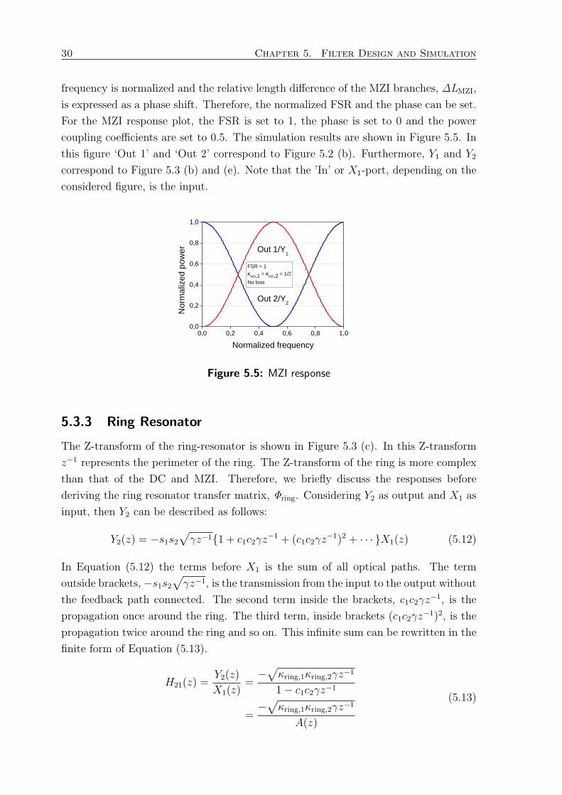
30 Chapter 5. Filter Design and Simulation
frequency is normalized and the relative length difference of the MZI branches, ∆LMZI,
is expressed as a phase shift. Therefore, the normalized FSR and the phase can be set.
For the MZI response plot, the FSR is set to 1, the phase is set to 0 and the power
coupling coefficients are set to 0.5. The simulation results are shown in Figure 5.5. In
this figure ‘Out 1’ and ‘Out 2’ correspond to Figure 5.2 (b). Furthermore, Y1 and Y2
correspond to Figure 5.3 (b) and (e). Note that the ’In’ or X1-port, depending on the
considered figure, is the input.
0 , 0 0 , 2 0 , 4 0 , 6 0 , 8 1 , 00 , 0
0 , 2
0 , 4
0 , 6
0 , 8
1 , 0
F S R = 1κM Z I , 1 = κM Z I , 2 = 1 / 2N o l o s s
O u t 2 / Y 2
Norm
alized
powe
r
N o r m a l i z e d f r e q u e n c y
O u t 1 / Y 1
Figure 5.5: MZI response
5.3.3 Ring Resonator
The Z-transform of the ring-resonator is shown in Figure 5.3 (c). In this Z-transform
z−1 represents the perimeter of the ring. The Z-transform of the ring is more complex
than that of the DC and MZI. Therefore, we briefly discuss the responses before
deriving the ring resonator transfer matrix, Φring. Considering Y2 as output and X1 as
input, then Y2 can be described as follows:
Y2(z) = −s1s2
√γz−11 + c1c2γz
−1 + (c1c2γz−1)2 + · · · X1(z) (5.12)
In Equation (5.12) the terms before X1 is the sum of all optical paths. The term
outside brackets, −s1s2
√γz−1, is the transmission from the input to the output without
the feedback path connected. The second term inside the brackets, c1c2γz−1, is the
propagation once around the ring. The third term, inside brackets (c1c2γz−1)2, is the
propagation twice around the ring and so on. This infinite sum can be rewritten in the
finite form of Equation (5.13).
H21(z) =Y2(z)
X1(z)=−√κring,1κring,2γz−1
1− c1c2γz−1
=−√κring,1κring,2γz−1
A(z)
(5.13)

5.3. Available Components for Design 31
Consider now Y1 as output and X1 as input. Then Y1 can be described as in
Equation (5.14). In this equation the terms before X1 is the sum of all optical paths.
The c1 term is the transmission from the input to the output without the feedback path
connected. The −s21c2γz
−1 term is the transmission from the input to the output once
around the ring and so on. The corresponding transfer function is given by Equation
(5.15).
Y1(z) =[c1 − s2
1c2γz−11 + c1c2γz
−1 + (c1c2γz−1)2 + · · ·
]X1(z)
=
[c1 − c2γz−1
1− c1c2γz−1
]X1(z)
(5.14)
H11(z) =Y1(z)
X1(z)=
[c1 − c2γz−1
1− c1c2γz−1
]=B(z)
A(z)
(5.15)
Similarly, one can obtain H12 and H22 and derive the relations in Equations (5.16)
and (5.17). In Equation (5.17) BR(z) is the reverse polynomial of B(z); the superscript
R denotes reverse polynomial.
H12(z) = H21(z) =−√κring,1κring,2γz−1
A(z)(5.16)
H22(z) =Y2(z)
X2(z)=
[c2 − c1γz−1
1− c1c2γz−1
]=−BR(z)
A(z)
(5.17)
Now the transfer functions are derived, the frequency responses of the ring can
be considered. Consider the case where the coupling coefficients are equal, κring,1 =
κring,2 = κ, then the square magnitude response of H21(ω) is given by Equation (5.18).
A transmission peak occurs at ω = φ, where φ is the phase of the ring. When the ring
is lossless, the peak transmission is 1 (γ = 1).
∣∣H21(ω)∣∣2 =
κ2γ
1− 2c2γ cos(ω − φ) + c4γ2(5.18)
Now having the response of H21(ω), it is easy to derive the response H11(ω), since
they are complementary. Furthermore, since κring,1 = κring,2 = κ, −BR(z) = B(z)
resulting in H22(z) = H11(z).
The frequency responses are simulated in LabVIEW 8.5. In the simulation program,
the frequency and the radius of the ring, Rring, are normalized. Therefore, the FSR

32 Chapter 5. Filter Design and Simulation
and the phase can be set. Since a large FSR is related to a small delay, a large FSR
corresponds to a small ring radius Rring. For the response plot, the FSR is set to 1, the
phase is set to 0 and the power coupling coefficients are set to κring,1 = κring,2 = 0.33.
Besides, the loss is set to zero (γ = 1).
Figure 5.6 shows the response plot of H11 and H21. In the figure ‘Through’ (H11)
0 , 0 0 , 2 0 , 4 0 , 6 0 , 8 1 , 00 , 0
0 , 2
0 , 4
0 , 6
0 , 8
1 , 0
F S R = 1κr i n g , 1 = κr i n g , 2 = 1 / 3N o l o s s
Norm
alized
powe
r
N o r m a l i z e d f r e q u e n c y
D r o p /Y 2
T h r o u g h /Y 1
Figure 5.6: Response of ring with two couplers
and ‘Drop’ (H21) correspond to Figure 5.2 (c). Furthermore, Y1 and Y2 correspond to
Figure 5.3 (c) and (f). Note that the ’In’ or X1-port, depending on the considered
figure, is the input.
Since the H11-response is high for a large frequency range and the H21-response
for a small frequency range, they are respectively denoted as ‘Through’-and ‘Drop’-
responses. The H12-response is called ‘Add’-response, since another signal with the
same carrier frequency as that of the ‘Drop’-signal can be added via port X2. The
width of the peak or valley is related to the power coupling coefficients. The smaller
the coupling coefficients, the narrower the peak or valley. The loss in the ring will
impact the peak hight or valley depth.
Just as in the case of the MZI and the DC, the 2 × 2 transfer matrix of the ring-
resonator,Φring, is presented. The 2× 2 transfer matrix of the ring resonator is shown
in Figure 5.3 (f). After doing some mathematically operations, the transfer matrix is
derived from Equations (5.15), (5.16) and (5.17) as:[Y1(z)
X1(z)
]= Φring(z)
[X2(z)
Y2(z)
](5.19)
where Φring(z) =1
−√κring,1κring,2γz−1
[AR(z) B(z)
BR(z) A(z)
]
5.4. Slope Detector Design 33
5.4 Slope Detector Design
At least two components for the slope detector design are needed to obtain the required
branch responses of Figure 4.2 (b). Considering their output responses, it is impossible
to obtain the required response using only one of the components of Section 5.3. There-
fore, two relative simple filter designs, in which a directional coupler equally divides
the input power, are used as starting point for the actual design.
5.4.1 DC Power Divider and Two MZIs
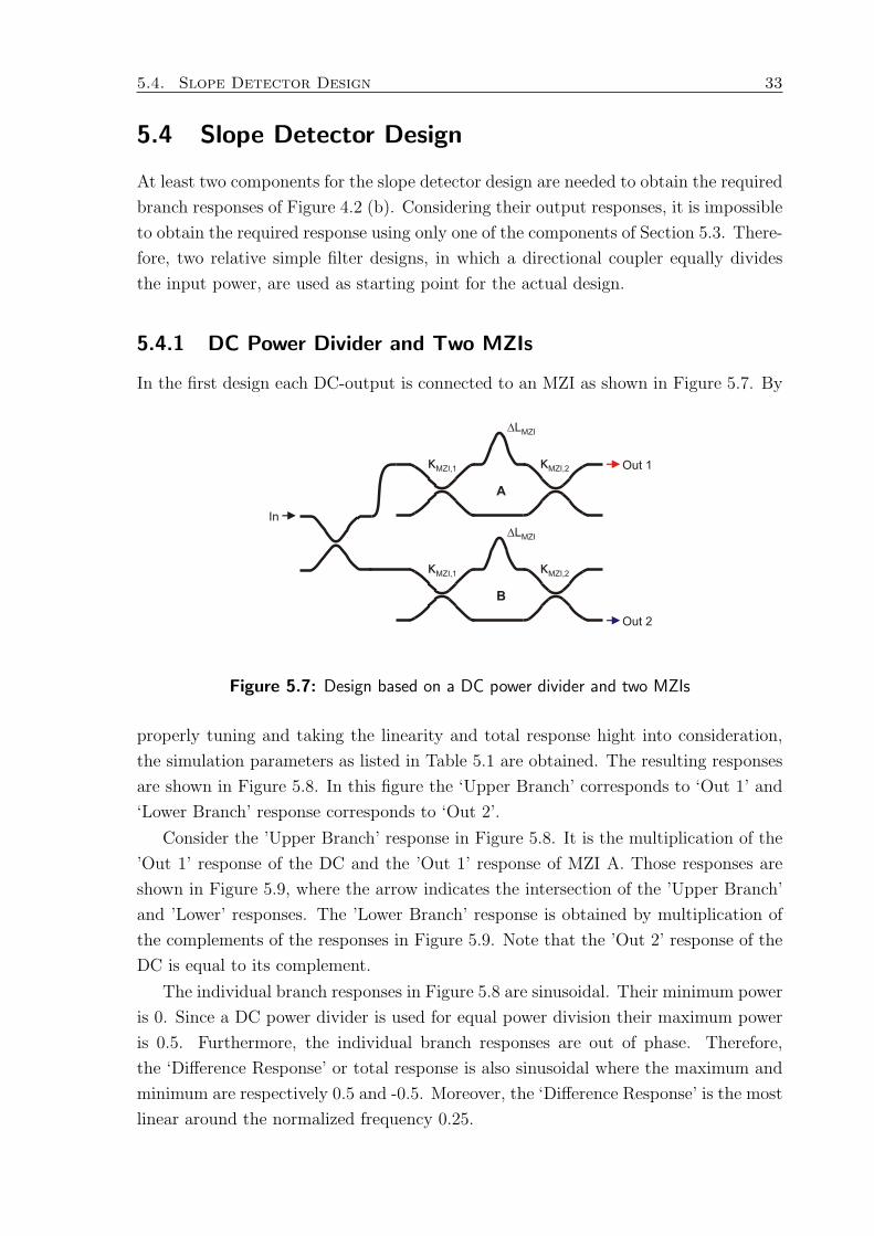
In the first design each DC-output is connected to an MZI as shown in Figure 5.7. By
Figure 5.7: Design based on a DC power divider and two MZIs
properly tuning and taking the linearity and total response hight into consideration,
the simulation parameters as listed in Table 5.1 are obtained. The resulting responses
are shown in Figure 5.8. In this figure the ‘Upper Branch’ corresponds to ‘Out 1’ and
‘Lower Branch’ response corresponds to ‘Out 2’.
Consider the ’Upper Branch’ response in Figure 5.8. It is the multiplication of the
’Out 1’ response of the DC and the ’Out 1’ response of MZI A. Those responses are
shown in Figure 5.9, where the arrow indicates the intersection of the ’Upper Branch’
and ’Lower’ responses. The ’Lower Branch’ response is obtained by multiplication of
the complements of the responses in Figure 5.9. Note that the ’Out 2’ response of the
DC is equal to its complement.
The individual branch responses in Figure 5.8 are sinusoidal. Their minimum power
is 0. Since a DC power divider is used for equal power division their maximum power
is 0.5. Furthermore, the individual branch responses are out of phase. Therefore,
the ‘Difference Response’ or total response is also sinusoidal where the maximum and
minimum are respectively 0.5 and -0.5. Moreover, the ‘Difference Response’ is the most
linear around the normalized frequency 0.25.

34 Chapter 5. Filter Design and Simulation
Table 5.1: Simulation parameters for design of Figure 5.7 (DC power divider and two
MZIs)
Component Parameter Symbol Value
DC DC power coupling coefficient κDC 0.5
MZI A
MZI power coupling coefficient 1 κMZI,1 0.5
MZI power coupling coefficient 2 κMZI,2 0.5
MZI free spectral range FSRMZI 1
MZI phase φMZI 0
MZI B
MZI power coupling coefficient 1 κMZI,1 0.5
MZI power coupling coefficient 2 κMZI,2 0.5
MZI free spectral range FSRMZI 1
MZI phase φMZI 0
0 . 0 0 . 1 0 . 2 0 . 3 0 . 4 0 . 5- 0 . 8- 0 . 6- 0 . 4- 0 . 20 . 00 . 20 . 40 . 60 . 8
Powe
r (a.u.
)
F r e q u e n c y ( a . u . )
U p p e r B r a n c h L o w e r B r a n c h D i f f e r e n c e R e s p o n s e
(a)
0 . 0 0 . 1 0 . 2 0 . 3 0 . 4 0 . 50 . 00 . 10 . 20 . 30 . 40 . 50 . 60 . 70 . 80 . 91 . 0
Powe
r (a.u.
)
F r e q u e n c y ( a . u . )
U p p e r B r a n c h L o w e r B r a n c h S u m R e s p o n s e
(b)
Figure 5.8: Sum Response (a) and Difference Response (b) of design of Figure 5.7 (DC
power divider and two MZIs)
The nonlinear behavior is not the key element, since measures as predistortion can
be taken to improve the linearity [5]. However, a discussion about predistortion is
beyond the scope of this report. The overlap of the branches is more of concern. Since
this overlap results in an increase of the average detected optical power, the noise power
will increase. The more overlap, the worser the noise performance will be. The ‘Sum
Response’ gives an indication of the overlap of the individual branches. In the case of
the ideal branch responses in Figure 4.2, the overlap is zero. The ideal ’Sum Response’
is then zero at the carrier frequency. For the lower frequencies the ‘Sum Response’ is
equal to the response of ’Branch 2’. For the higher frequencies the ‘Sum Response’ is
equal to the response of ’Branch 1’.

5.4. Slope Detector Design 35
0 . 0 0 . 2 0 . 4 0 . 6 0 . 8 1 . 00 . 0
0 . 2
0 . 4
0 . 6
0 . 8
1 . 0No
rmaliz
ed po
wer
N o r m a l i z e d f r e q u e n c y
O u t 1
(a)
0 . 0 0 . 2 0 . 4 0 . 6 0 . 8 1 . 00 . 0
0 . 2
0 . 4
0 . 6
0 . 8
1 . 0
Norm
alized
powe
r
N o r m a l i z e d f r e q u e n c y
O u t 1
(b)
Figure 5.9: (a) ’Out 1’ response of the DC and (b) ’Out 1’ response of MZI A in Figure 5.7
(DC power divider and two MZIs)
The ‘Sum Response’ of the simulated design is constant and equal to the maximum
power of a single branch (0.5). In other words, since the individual responses do not
have the flat parts as required for HWR this design is not suitable for slope detection.
Note that the ’Sum Response’ and ‘Difference Response’ of this design are the same
as those of a single MZI, apart from a factor two. The ’Sum Response’ and ‘Difference
Response’ of a single MZI can be respectively obtained by addition and subtraction of
the responses in Figure 5.5.
5.4.2 DC Power Divider and Two Ring-Resonators
In this design, each DC-output is connected to a ring-resonator as shown in Figure 5.10.
The simulation parameters for this design are listed in Table 5.2. The same tuning
procedure as in the previous design is used. The FSR is by accident set to 0.5 instead
of 1. Since the FSR parameter is normalized and equal for both rings, the choice of
its value does not affect the fabrication of the filter. When the rings had different
FSR values, only the ratio of these values would be important for the fabrication.
To simulate the effect of ring loss, the power loss is set to 0.175 dB per round trip,
corresponding to a loss of 0.1 dB/cm for an FSR of 25 GHz.
The simulated responses are shown in Figure 5.4.2. In this figure the ’Upper Branch’
corresponds to ’Out 1’ and ’Lower Branch’ corresponds to ’Out 2’. Consider the ’Upper
Branch’ response. It is the multiplication of the ’Out 1’ response of the DC and the
’Drop’ response of Ring A. Those responses are shown in Figure 5.12, where the arrow
indicates the intersection of the ’Upper Branch’ and ’Lower Branch’ responses. The
’Lower Branch’ response is obtained in a similar way, but then the ’Drop’ response is
shifted in frequency.

36 Chapter 5. Filter Design and Simulation
Figure 5.10: Design based on a DC power divider and two ring-resonators
Table 5.2: Simulation parameters for design of Figure 5.10 (DC power divider and two
ring-resonators)
Component Parameter Symbol Value
DC DC power coupling coefficient κDC 0.5
Ring A
ring power coupling coefficient 1 κring,1 0.33
ring power coupling coefficient 2 κring,2 0.33
ring round trip loss lring 0.175 (dB)
ring free spectral range FSRring 0.5
ring round trip phase φring 0
Ring B
ring power coupling coefficient 1 κring,1 0.33
ring power coupling coefficient 2 κring,2 0.33
ring round trip loss lring 0.175 (dB)
ring free spectral range FSRring 0.5
ring round trip phase φring 1.13 (rad)
The individual branch responses in Figure 5.4.2 have a Gaussian shape. The indi-
vidual responses are a better approximation of the ideal branch responses of Figure 4.2
(b) than the individual responses of the MZI-based design of Figure 5.8. As a result,
the ‘Sum Response’ is lower around the intersection of the individual branches. How-
ever, the overlap of the individual branches is large at the intersection. Furthermore,
the ’Difference Response’ maxima are low. Mainly due to the power splitting by the
DC, the normalized maximum and minimum respectively are 0.4 and -0.4.
It is noted that the shape of the individual branch responses are similar to the
theoretical responses of a balanced RF-frequency discriminator [9]. In other words,
this design is the optical equivalent of the RF-frequency discriminator.

5.4. Slope Detector Design 37
0 . 4 0 0 . 4 2 0 . 4 4 0 . 4 6 0 . 4 8 0 . 5 0 0 . 5 2- 0 . 8- 0 . 6- 0 . 4- 0 . 20 . 00 . 20 . 40 . 60 . 8
Powe
r (a.u.
)
F r e q u e n c y ( a . u . )
U p p e r B r a n c h L o w e r B r a n c h D i f f e r e n c e R e s p o n s e
(a)
0 . 4 0 0 . 4 2 0 . 4 4 0 . 4 6 0 . 4 8 0 . 5 0 0 . 5 20 . 00 . 10 . 20 . 30 . 40 . 50 . 60 . 70 . 80 . 91 . 0
Powe
r (a.u.
)
F r e q u e n c y ( a . u . )
U p p e r B r a n c h L o w e r B r a n c h S u m R e s p o n s e
(b)
Figure 5.11: Simulated Difference Response (a) and Sum Response (b) of design in Fig-
ure 5.10 (DC power divider and two ring-resonators)
0 . 0 0 . 2 0 . 4 0 . 6 0 . 8 1 . 00 . 0
0 . 2
0 . 4
0 . 6
0 . 8
1 . 0
Norm
alized
powe
r
N o r m a l i z e d f r e q u e n c y
O u t 1
(a)
0 . 0 0 . 2 0 . 4 0 . 6 0 . 8 1 . 00 . 0
0 . 2
0 . 4
0 . 6
0 . 8
1 . 0
Norm
alized
powe
r
N o r m a l i z e d f r e q u e n c y
D r o p
(b)
Figure 5.12: (a) ’Out 1’ response of the DC and (b) ‘Drop’ response of Ring A in Fig-
ure 5.10 (DC power divider and two ring-resonators)
5.4.3 Three Ring-Resonators
Based on the simulations of two previous designs, a new design is made consisting of
three ring-resonators as shown in Figure 5.13.
This design is similar to that of Figure 5.10, but the DC is replaced by a ring-
resonator in order to increase the maximum transmission. The simulation parameters
for this design are listed in Table B.1 in Appendix B. The simulation results are shown
in Figure 5.14.
Consider the ‘Upper Branch’ response in Figure 5.14. It is the multiplication of
the ’Drop’ response of Ring A and the ‘Through’ response of Ring B. Both responses

38 Chapter 5. Filter Design and Simulation
Figure 5.13: Design based on three ring-resonators
are shown in Figure 5.15. The ’Lower Branch’ response is obtained by multiplying the
’Through’ response of Ring A and the ‘Drop’ response of Ring C. By properly choosing
the settings of Ring C in the ‘Lower Branch’, the branch responses have shapes which
are each other mirror image. The plane of mirror is at the intersection.
0 , 4 0 0 , 4 2 0 , 4 4 0 , 4 6 0 , 4 8 0 , 5 0 0 , 5 2- 1 , 0- 0 , 8- 0 , 6- 0 , 4- 0 , 20 , 00 , 20 , 40 , 60 , 81 , 0
Powe
r (a.u.
)
F r e q u e n c y ( a . u . )
U p p e r B r a n c h L o w e r B r a n c h D i f f e r e n c e R e s p o n s e
(a)
0 . 4 0 0 . 4 2 0 . 4 4 0 . 4 6 0 . 4 8 0 . 5 0 0 . 5 20 . 00 . 10 . 20 . 30 . 40 . 50 . 60 . 70 . 80 . 91 . 0
Powe
r (a.u.
)
F r e q u e n c y ( a . u . )
U p p e r B r a n c h L o w e r B r a n c h S u m R e s p o n s e
(b)
Figure 5.14: Simulated Difference Response (a) and Sum Response (b) of the design in
Figure 5.13 (three ring-resonators)
Figure 5.14 shows that the maximum transmission per branch is increased to ap-
proximately 0.8. As a result, the ’Difference Response’ has 0.8 and -0.8 as maximum
and minimum, respectively. Furthermore, the individual branch responses both have
a zero, when the complementary branch response is maximum. However, as indicated
by the ‘Sum Response’ there is still an overlap at the intersection of the individual
branches.

5.4. Slope Detector Design 39
0 . 0 0 . 2 0 . 4 0 . 6 0 . 8 1 . 00 . 0
0 . 2
0 . 4
0 . 6
0 . 8
1 . 0No
rmaliz
ed po
wer
N o r m a l i z e d f r e q u e n c y
D r o p
(a)
0 . 0 0 . 2 0 . 4 0 . 6 0 . 8 1 . 00 . 0
0 . 2
0 . 4
0 . 6
0 . 8
1 . 0
Norm
alized
powe
r
N o r m a l i z e d f r e q u e n c y
T h r o u g h
(b)
Figure 5.15: (a) ’Drop’ response of Ring A and (b) ‘Through’ response of Ring B in
Figure 5.13 (three ring-resonators)
5.4.4 Five Ring-Resonators
The response of the preceding design has a large overlap, which can be reduced by
adding zeros in the responses. This is realized by adding a bar coupled ring-resonator
in both branches as is shown in Figure 5.16. The zero in each branch response is placed
close to the intersection of both branch responses, where in the ideal case will be the
transition from the flat to linear part. Besides reducing the overlap, the part which
has to carry out the FM-to-IM conversion is also lowered, thereby reducing the slope.
By making the FSR of the added rings smaller, the frequency band impacted by the
zero is reduced. The FSR of the added rings is set equal to half times the FSR of
the other rings. The FSR of the added rings is then still larger than the interesting
range for frequency discrimination. In other words, we do not have to bother about
an extra zero besides the desired added zero in the frequency range of the frequency
discriminator. As a result, the part which has to carry out the FM-to-IM conversion is
less lowered than in the case of no halving of FSR. Moreover, there is still a reduction
in the overlap.
In
êring,1
êring,2
2Rring
êring,1
êring,2
Rring êring,1
êring,2
Rring êring,1
êring,2
Rringêring,1
êring,2
2Rring
Out 2
Out 1
D
CB
E
A
Figure 5.16: Design based on five ring-resonators

40 Chapter 5. Filter Design and Simulation
The simulation parameters for this design are listed in Tables B.2 and B.3 in Ap-
pendix B. The simulation results are shown in Figure 5.17. Consider the ‘Upper Branch’
response in this figure. It is the multiplication of the ‘Drop’ response of Ring A and the
‘Through’ responses of Ring B and C. The ‘Drop’ and ‘Through’ responses of respec-
tively Ring A and Ring B are the same as in Figures 5.15(a) and 5.15(b). Furthermore,
the ‘Through’ response of Ring C is shown in Figure 5.18.
0 , 4 0 0 , 4 2 0 , 4 4 0 , 4 6 0 , 4 8 0 , 5 0 0 , 5 2- 0 , 8- 0 , 6- 0 , 4- 0 , 20 , 00 , 20 , 40 , 60 , 8
U p p e r B r a n c h L o w e r B r a n c h D i f f e r e n c e R e s p o n s e
Powe
r (a.u.
)
F r e q u e n c y ( a . u . )(a)
0 . 4 0 0 . 4 2 0 . 4 4 0 . 4 6 0 . 4 8 0 . 5 0 0 . 5 20 . 00 . 10 . 20 . 30 . 40 . 50 . 60 . 70 . 80 . 91 . 0
U p p e r B r a n c h L o w e r B r a n c h S u m R e s p o n s e
Powe
r (a.u.
)
F r e q u e n c y ( a . u . )(b)
Figure 5.17: Simulated Difference (a) and Sum Response (b) of the design in Figure 5.16
(five ring-resonators)
0 . 0 0 . 2 0 . 4 0 . 6 0 . 8 1 . 00 . 0
0 . 2
0 . 4
0 . 6
0 . 8
1 . 0
Norm
alized
powe
r
N o r m a l i z e d f r e q u e n c y
T h r o u g h
Figure 5.18: ‘Through’ response of Ring C in Figure 5.16 (five ring-resonators)
In Figure 5.16 the number of cross couplings and bar couplings are equal per branch.
By properly choosing the settings of the unshared rings in the ‘Lower Branch’, the
branch responses have shapes which are each other mirror image. The plane of mirror
is at the intersection of the responses.
Figure 5.17 shows that the maximum transmission of each branch response is re-
duced by 0.1 to 0.7, respectively resulting in 0.7 and −0.7 as maximum and minimum

5.4. Slope Detector Design 41
of the ‘Difference Response’. Furthermore, the ‘Difference Response’ has an increase
in nonlinearities. For the purpose of comparison, a dashed straight line is drawn in
Figures 5.14(a) and 5.17(a). However, the overlap is indeed reduced.
When adding another ring-resonator in both branches, the residual overlap can
be further reduced. Besides, the ’Difference Response’ becomes more linear, since
the residual overlap gives rise to the nonlinearities in the ’Difference Response’, as is
indicated in Figure 5.17(a). However, the addition of these extra ring-resonators goes
beyond the scope of this report.

42 Chapter 5. Filter Design and Simulation

Chapter 6
Measurements
In this chapter the measurements of the laser FM-characteristics are discussed. Since
it is not possible to fabricate the designed filter of the preceding chapter in the project,
DWDM-filters are used instead. They are employed in such a way that the concept of
the FM-slope detection AOL can be tested.
Before verifying the concept, the laser P-I curve is determined, giving the relation
between optical power and laser bias current. Next, the temperature and current
dependences of the laser wavelength are determined for the purpose of tuning. Since
the DWDM-filters are not tunable, the laser wavelength is tuned. Furthermore, the
DWDM-filter transfer is measured by varying the laser wavelength. Using this DWDM-
filter transfer, the FM-characteristics are determined. Moreover, the feasibility of the
HWR is determined
6.1 Semiconductor Laser Diode P-I Curve
6.1.1 Measurement Setup
The relation between optical power and bias current is measured using the setup in
Figure 6.1. The used laser is from Eudyna and its characteristics as specified by
the manufacturer are listed in Tabel 6.1. The laser is mounted on an ILX LDM
Table 6.1: Eudyna SLD characteristics
Parameter Value Unit
Type FLD5F15CX J9310F -
Wavelength (T: 20 - 35 C) 1552.52 nm
Maximum current 150 mA
Maximum power (minimum) 10.0 mW
laser diode mounting device, which is connected to the ILX Lightwave LDC 3724 SLD
43

44 Chapter 6. Measurements
controller.Using this controller, the bias current is varied in the range from 1 to 140
mA and the laser ambient temperature is kept constant at 25.01 C. The optical power
is detected by an optical head which is connected to the power meter. The optical head
has a maximum optical input power of 3 dBm. Therefore, the optical power of the laser
is attenuated by a variable optical attenuator (VOA) before detection. The important
characteristics and settings of the VOA and power meter are listed in Tabel 6.2.
Table 6.2: Characteristics and settings of the VOA and power meter in Figure 6.1
.
Device Parameter Value Unit
VOA
Type HP 8157A -
Wavelength 1552 nm
Attenuation See Figure 6.2 -
Insertion loss 2.35 dB
Power meter
Type optical head HP 81521B -
Type meter HP 8152A -
Wavelength 1552 nm
Maximum input power 3 dBm
6.1.2 Measurement Results
The measurement results for an attenuation of 10 and 20 dB are shown in Figure 6.2,
where the optical power is the calculated power after correction for the VOA atten-
uation. The inset shows the P-I curves around threshold in more detail. From this
inset can be determined that the threshold current of the laser is 11 mA. Furthermore,
calculating the slope using the bias currents of 12 and 20 mA and the corresponding
optical power, one obtains a slope efficiency sl of 0.19 W/A for both curves.
A line with the calculated slope going through the threshold point is plotted in the
main graph. From the plotted line can be observed that the relation between optical
power and bias current is not linear for both curves. The ‘10 dB attenuation’ curve
starts deviating from the straight line around a bias current of 90 mA. Furthermore,
the ‘20 dB attenuation’ curve starts deviating from the straight line around 80 mA.
In the ‘20 dB attenuation’ measurements the maximum detected optical power is 0.23
mW corresponding to −6.38 dBm, roughly 10 dB below the optical head maximum
input power. In other words, the optical head is not saturated for a laser bias current
of 80 mA in the ‘20 dB attenuation’ measurements. Therefore, it can be concluded
that the nonlinear behavior is a laser characteristic. The difference of 10 mA in the
starting points of the deviation is probably due to a measurement inaccuracy, since a
gap of 0.5 mW appears between both curves at the end of the measurement range (140
mA) in the main graph.
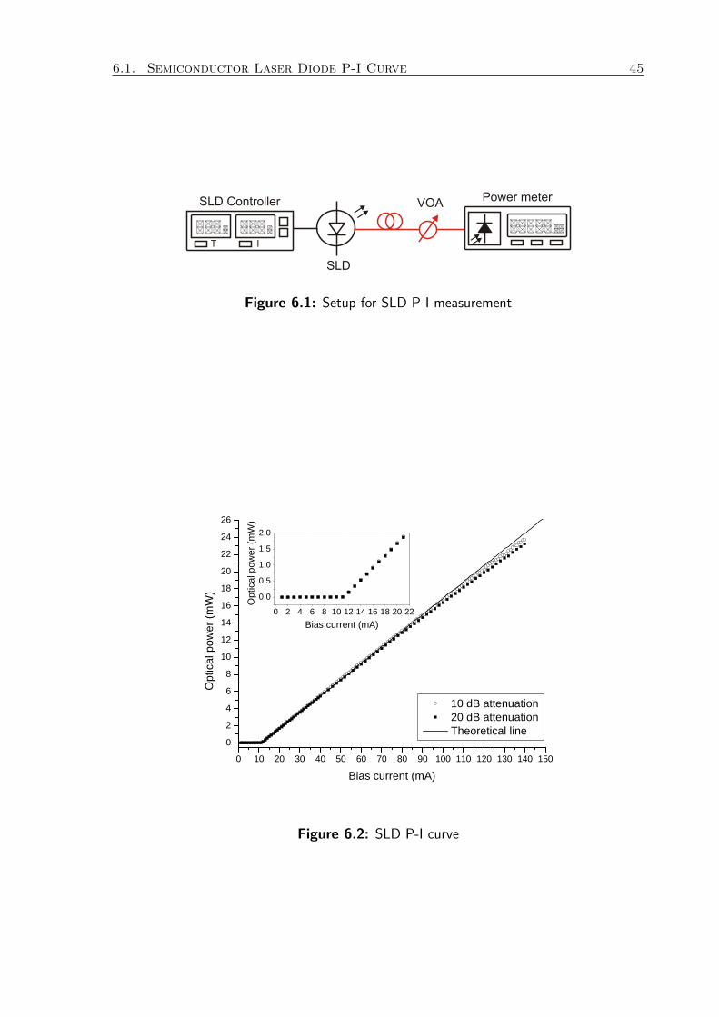
6.1. Semiconductor Laser Diode P-I Curve 45
Figure 6.1: Setup for SLD P-I measurement
0 1 0 2 0 3 0 4 0 5 0 6 0 7 0 8 0 9 0 1 0 0 1 1 0 1 2 0 1 3 0 1 4 0 1 5 002468
1 01 21 41 61 82 02 22 42 6
1 0 d B a t t e n u a t i o n 2 0 d B a t t e n u a t i o n T h e o r e t i c a l l i n e
Optica
l pow
er (m
W)
B i a s c u r r e n t ( m A )
0 2 4 6 8 1 0 1 2 1 4 1 6 1 8 2 0 2 20 . 00 . 51 . 01 . 52 . 0
Optica
l pow
er (m
W)
B i a s c u r r e n t ( m A )
Figure 6.2: SLD P-I curve

46 Chapter 6. Measurements
6.2 Temperature and Current Dependences of SLD Wave-
length
6.2.1 Measurement Setup
The temperature dependencies of the Eudyna SLD wavelength are determined using
the measurement setup of Figure 6.3. Again, the laser is mounted on an ILX LDM
laser diode mounting device. Using the SLD controller, the laser temperature and laser
current are both varied. The temperature is varied in the range from 20.0 to 33.0 C
with steps of 0.5 C and the current is varied in the range from 15 to 140 mA with steps
of 5 mA. The wavelength of the laser is measured by the HP 70951A optical spectrum
analyzer (OSA) of which the settings are listed in Table 6.3.
Figure 6.3: Experimental setup for characterization temperature and current sensitivity of
SLD-wavelength
Table 6.3: Settings optical spectrum analyzer in Figure 6.3
Parameter Value Unit
Reference level 30.00 dBm
Sensitivity -41 dBm
Display scale 10.00 dB/div
Resolution bandwidth 0.1 nm
Video bandwidth 1 kHz
Sweeptime 50 msec
Center wavelength 1552.000 nm
Span 3.500 nm
6.2.2 Measurement Results
The measurement results are shown in Figure 6.4. The OSA has an absolute accuracy of
± 1 nm. Besides, it took a long time before the setup was stabilized after changing the
temperature or current and furthermore the stabilization times were random, requiring
user interaction during the measurements. Therefore, the measurements toke more

6.2. Temperature and Current Dependences of SLD Wavelength 47
than a day. As a consequence, the absolute accuracy of the OSA becomes observable as
gaps between curves and overlapping of curves. However, the tendencies are observable.
As is shown in Figure 6.4 the wavelength is a nonlinear function of the bias current.
For every temperature setting, the wavelength changes monotone over the range from
15 mA to 140 mA with the average total change of 0.356 nm corresponding to 44.5
GHz. Furthermore, the wavelength is a linear function of temperature, as is shown
in Figure 6.5 for a bias current of 75 mA. The average increase in wavelength for
an increase of 0.5 C for a fixed bias current is calculated. In this calculation the
temperature ranges from 20.0 to 24.0 C, 24.5 to 28.5 C and 32.0 to 33.0 C are
considered. That are the ranges which are free of gaps and overlaps. The measurement
data for the currents 15 mA and 140 mA of the first temperature range are listed in
Table 6.4 for the purpose of illustration. The calculated result is 0.055 nm per 0.5 C,
resulting in an average temperature sensitivity of 0.11 nm/C (corresponding to 13.7
GHz/C).
Since the wavelength is more sensitive in temperature than in current, the temper-
ature is used as wavelength tuning parameter.
0 2 0 4 0 6 0 8 0 1 0 0 1 2 0 1 4 01 5 5 0 . 81 5 5 0 . 91 5 5 1 . 01 5 5 1 . 11 5 5 1 . 21 5 5 1 . 31 5 5 1 . 41 5 5 1 . 51 5 5 1 . 61 5 5 1 . 71 5 5 1 . 81 5 5 1 . 91 5 5 2 . 01 5 5 2 . 11 5 5 2 . 21 5 5 2 . 31 5 5 2 . 41 5 5 2 . 51 5 5 2 . 61 5 5 2 . 71 5 5 2 . 8
Wave
length
(nm)
Figure 6.4: SLD wavelength characteristics

48 Chapter 6. Measurements
Table 6.4: Measurement data for the bias currents 15 mA and 140 mA for determining
the wavelength temperature dependence
I (mA) T (C) λ (nm) I (mA) T (C) λ (nm)
15.01
20.01 1550.867
139.87
20.01 1551.208
20.51 1550.924 20.51 1551.265
21.01 1550.981 21.01 1551.313
21.51 1551.029 21.51 1551.370
22.02 1551.073 22.02 1551.431
22.52 1551.138 22.52 1551.493
23.01 1551.204 23.01 1551.554
23.51 1551.261 23.51 1551.611
24.02 1551.313 24.02 1551.668
2 4 , 0 2 4 , 5 2 5 , 0 2 5 , 5 2 6 , 0 2 6 , 5 2 7 , 0 2 7 , 5 2 8 , 0 2 8 , 5 2 9 , 01 5 5 1 , 5 01 5 5 1 , 5 51 5 5 1 , 6 01 5 5 1 , 6 51 5 5 1 , 7 01 5 5 1 , 7 51 5 5 1 , 8 01 5 5 1 , 8 51 5 5 1 , 9 01 5 5 1 , 9 51 5 5 2 , 0 0
Wave
length
(nm)
Figure 6.5: SLD wavelength versus temperature
6.3 DWDM Filter Transfer and SLD FM Response
6.3.1 Measurement Setup
Since the laser has an IM-response besides the FM-response, the IM-response must be
known in order to determine the FM-response. The IM-response and the FM-response
are measured using the measurement setup of Figure 6.6. A network analyzer (NA)
provides the modulating RF-signal to the SLD. Then, the optical signal of the laser
is equally divided over two branches, an upper and a lower branch. The upper branch
is used as reference and is therefore denoted as reference link. It consists of a variable
optical attenuator, VOA 1, which tracks the DWDM-filter loss. In this way, the refer-
ence link tracks the curve of the DWDM-filter. Furthermore, the attenuator enables

6.3. DWDM Filter Transfer and SLD FM Response 49
blocking of the reference link. The lower branch consists of the DWDM-filter and is
therefore denoted as DWDM-link. This link also has a variable optical attenuator,
VOA 2. The attenuator is to prevent the optical power to exceed the detector optical
power limit and to enable blocking of the link. The BPD detects one of the links or
both links, depending on the settings of the VOAs. The bias-T blocks the DC compo-
nents in the path to the NA. Furthermore, the DC-output of the bias-T is connected
to a multimeter to measure the BPD dc-current.
Figure 6.6: Measurement setup for determining the laser FM-characteristics
The measurement procedure starts by setting the temperature and current of the
SLD. Next, the DWDM-link is operated in CW-mode and the detected dc-current is
measured. Subsequently, both links are operated in CW-mode for tuning the atten-
uation of the reference link. It is tuned such that the dc-current of the BPD is zero.
This results in equal laser IM-responses in both links when measuring the responses of
the links. Then, the laser IM-response passing through the DWDM-link is measured
by blocking the DWDM-link and operating the NA in the S21 mode. Furthermore, the
converted FM-response in addition to the laser IM-response is measured by blocking
the reference link and operating the NA in the S21 mode. Finally, the laser temperature
is set to the next value in order to change the laser wavelength and the procedure is
repeated. During the measurements the laser current is not changed.
The used SLD, its mounting device and its controller in the setup of Figure 6.6 are
the same as in the previous measurements. The laser bias current is set to 75.00 mA,
such that the optical power after power splitting does not exceed the maximum optical

50 Chapter 6. Measurements
input power of a single photodetector (10 dBm). The steps in temperature are 0.1 C
and the range depends on the measurement, as will be seen later on. The details of
the other components are listed in Table 6.5 and the settings of the NA are listed in
Table 6.6. Furthermore, two AFOP DWDM-filters are available for the measurements.
Table 6.5: Details of components in measurement setup in Figure 6.6
Component Type Remarks
NAAgilent Technologies N5230A See Table 6.6
PNA-L Network Analyzer
VOA 1 ANDO Optical Variable Attenuator AQ-3105 Mechanical tuning
VOA 2Hewlett Packard Optical Attenuator HP 8157A See Table 6.2, atten-
uation: set to 3.00 dB
BPDDiscovery Semiconductors Rpd D 1: 0.64 A/W
Balanced Photodetector DSC710 Rpd D 2: 0.69 A/W
DC power supplyBSI PSM 3/2A 3CH Multi Channels Channel 1:
High Performance Regulated DC Power Supply set to 10.0 V
Bias T Ortel Corperation BN-2 100 kHz - 11 GHz -
Multimeter Hewlett Packard Multimeter HP34401A DC-current mode
Table 6.6: Settings of network analyzer in measurement setup in Figure 6.6
Parameter Value Unit
Output power 10.000 dBm
Reference level −48.00 dBm
Display scale 10.00 dB/div
Start frequency 10.0000 MHz
Stop frequency 4.00000 GHz
Sweeptime 100.000 msec
Sweep bandwidth 50.0 kHz
Sweep type linear -
Number of points 1024 -
Averaging off -
6.3.2 Measurement Results
Channel Transfer and Reference Responses
First of all, the filter transfer is determined in order to determine the interesting temper-
ature ranges for the response measurements of the reference link and DWDM-link. The

6.3. DWDM Filter Transfer and SLD FM Response 51
1 6 1 7 1 8 1 9 2 0 2 1 2 2 2 3 2 4 2 50 . 0
- 0 . 2- 0 . 4- 0 . 6- 0 . 8- 1 . 0
DC cu
rrent
(mA)
1 6 1 7 1 8 1 9 2 0 2 1 2 2 2 3 2 4 2 5- 9 0- 8 0- 7 0- 6 0- 5 0- 4 0
S 21 (d
B)
Figure 6.7: Measured dc-current of Channel 32 of DWDM 1
filter transfer is determined by measuring the detected dc-current of the DWDM-link
in the absence of the modulation signal. Note that this current is linear proportional
to the detected optical power. Figure 6.7 shows the measurement results for channel
32 of DWDM 1. In this figure the current as function of temperature is plotted. The
interesting range for the measurements are around the temperatures of 18.11 C and
23.11 C. The temperatures of 18.11 C and 23.11 C, indicated by a drop line, are
the optical 3 dB points of the filter. Since the slopes are large at these points, the
FM-to-IM conversion efficiency is expected to be large at these points.
In order to determine the FM response, the measured reference link response is
subtracted from the measured DWDM-link response. Therefore, the relation between
the filter transfer and reference link response is discussed before the actual discussion
of the measurement results. The reference responses corresponding to the previous
discussed filter transfer are shown in Figure 6.8. A logarithmic as well as a linear plot
for eight RF frequencies are shown. As can be seen, all the reference response neatly
tracks the filter transfer. In the linear plot the reference responses are decreasing in
the passband region, as a result of the not fully flat passband. Moreover, from the
logaritmic plot can be determined that the responses are within 6 dB to each other.
This indicates that the frequency band from 0.50 to 4.0 GHz is within the 3 dB optical
bandwidth of the modulation device in case of IM.
FM responses
For the measurements on Channel 32 of DWDM 1, the temperature is varied in the
range from 16.7 to 24.4 C. The S21 measurement results of both links are shown in
Figure 6.9 for eight temperature settings. The selection of temperatures is based on the
probed position of the channel transfer. The response curves corresponding to same
channel transfer loss or average detected optical power have the same line style and
color. In the figure the measure for average detected optical power, in the absence of
modulation signal, is the detected dc-current. For example, the reference link response
and corresponding DWDM-link response measured at a temperature of 18.62 C have
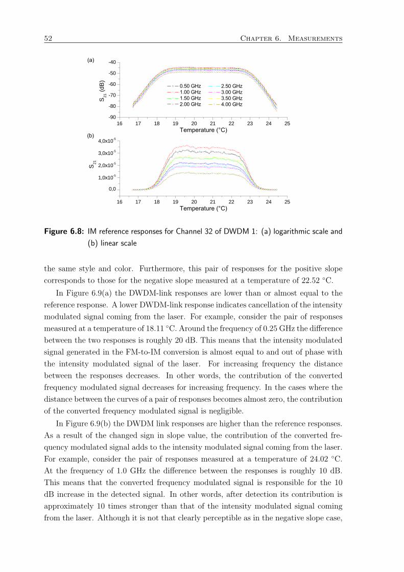
52 Chapter 6. Measurements
1 6 1 7 1 8 1 9 2 0 2 1 2 2 2 3 2 4 2 50 , 0
1 , 0 x 1 0 - 5
2 , 0 x 1 0 - 5
3 , 0 x 1 0 - 5
4 , 0 x 1 0 - 5
S 21
1 6 1 7 1 8 1 9 2 0 2 1 2 2 2 3 2 4 2 5- 9 0- 8 0- 7 0- 6 0- 5 0- 4 0
S 21
(dB)
Figure 6.8: IM reference responses for Channel 32 of DWDM 1: (a) logarithmic scale and
(b) linear scale
the same style and color. Furthermore, this pair of responses for the positive slope
corresponds to those for the negative slope measured at a temperature of 22.52 C.
In Figure 6.9(a) the DWDM-link responses are lower than or almost equal to the
reference response. A lower DWDM-link response indicates cancellation of the intensity
modulated signal coming from the laser. For example, consider the pair of responses
measured at a temperature of 18.11 C. Around the frequency of 0.25 GHz the difference
between the two responses is roughly 20 dB. This means that the intensity modulated
signal generated in the FM-to-IM conversion is almost equal to and out of phase with
the intensity modulated signal of the laser. For increasing frequency the distance
between the responses decreases. In other words, the contribution of the converted
frequency modulated signal decreases for increasing frequency. In the cases where the
distance between the curves of a pair of responses becomes almost zero, the contribution
of the converted frequency modulated signal is negligible.
In Figure 6.9(b) the DWDM link responses are higher than the reference responses.
As a result of the changed sign in slope value, the contribution of the converted fre-
quency modulated signal adds to the intensity modulated signal coming from the laser.
For example, consider the pair of responses measured at a temperature of 24.02 C.
At the frequency of 1.0 GHz the difference between the responses is roughly 10 dB.
This means that the converted frequency modulated signal is responsible for the 10
dB increase in the detected signal. In other words, after detection its contribution is
approximately 10 times stronger than that of the intensity modulated signal coming
from the laser. Although it is not that clearly perceptible as in the negative slope case,

6.3. DWDM Filter Transfer and SLD FM Response 53
- 1 0 1 2 3 4 5
- 8 0
- 7 0
- 6 0
- 5 0
- 4 0
D W D M - l i n kR e f e r e n c e l i n k
S 21 (d
B)
!
"
"
"
"
(a)
- 1 0 1 2 3 4 5
- 8 0
- 7 0
- 6 0
- 5 0
- 4 0
R e f e r e n c e l i n k
S 21 (d
B)
D W D M - l i n k
(b)
Figure 6.9: Measurement results DWDM 1 Channel 32: positive slope (a) and negative
slope (b)
the contribution of the converted frequency modulated signal decreases for increasing
frequency.
In Figure 6.10 the calculated FM responses are shown. In the calculation, the
measured responses are converted to linear scale first. Then, the DWDM-link response
is subtracted from its corresponding reference response. Next, the absolute value of
the resulting difference, the calculated FM response, is back-converted to logarithmic
scale and plotted. In this figure the same convention concerning the line style and
color of the response curves is used as in Figure 6.9. Besides the responses, the -3
dB level for every frequency response is plotted. This level is obtained by taking as
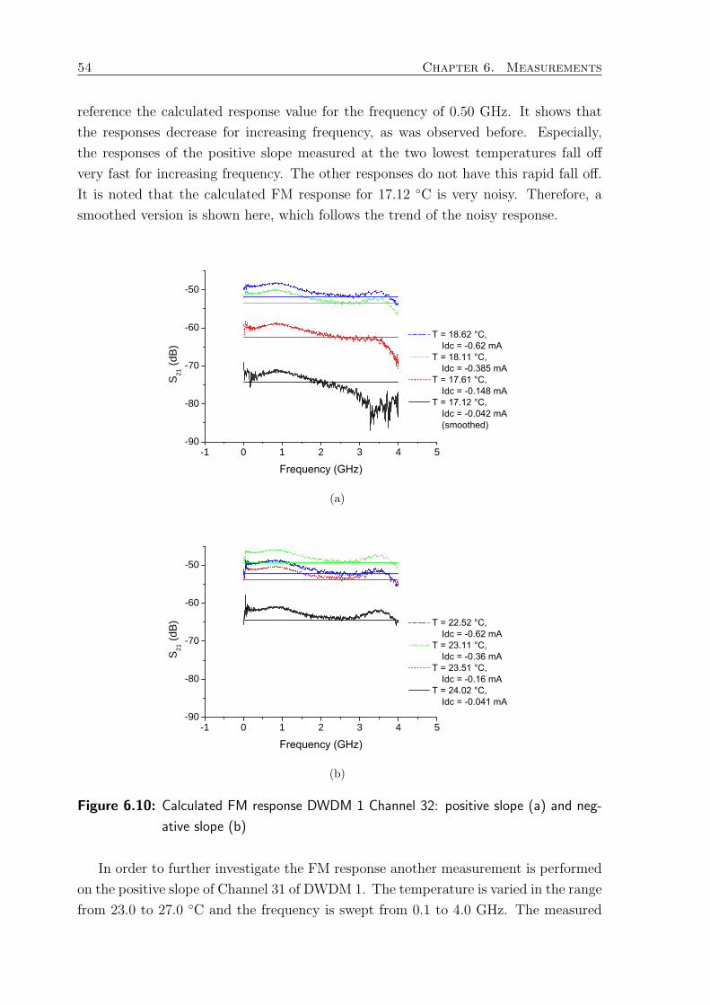
54 Chapter 6. Measurements
reference the calculated response value for the frequency of 0.50 GHz. It shows that
the responses decrease for increasing frequency, as was observed before. Especially,
the responses of the positive slope measured at the two lowest temperatures fall off
very fast for increasing frequency. The other responses do not have this rapid fall off.
It is noted that the calculated FM response for 17.12 C is very noisy. Therefore, a
smoothed version is shown here, which follows the trend of the noisy response.
- 1 0 1 2 3 4 5- 9 0
- 8 0
- 7 0
- 6 0
- 5 0
S 21 (d
B)
#$%
&
&
&
&!"
(a)
- 1 0 1 2 3 4 5- 9 0
- 8 0
- 7 0
- 6 0
- 5 0
S 21 (d
B)
(b)
Figure 6.10: Calculated FM response DWDM 1 Channel 32: positive slope (a) and neg-
ative slope (b)
In order to further investigate the FM response another measurement is performed
on the positive slope of Channel 31 of DWDM 1. The temperature is varied in the range
from 23.0 to 27.0 C and the frequency is swept from 0.1 to 4.0 GHz. The measured

6.3. DWDM Filter Transfer and SLD FM Response 55
reference link and DWDM-link responses and the calculated FM responses are shown
in Figure 6.11 for four different temperature settings. The reference responses as well
as the DWDM-link responses are similar to those corresponding to the positive slope of
Channel 32 of DWDM 1. All the calculated FM responses show a decreasing response
as function of frequency. The lowest response, the response for the temperature of
24.13 C, is smoothed and has the largest fall off.
- 1 0 1 2 3 4 5- 9 0
- 8 0
- 7 0
- 6 0
- 5 0
- 4 0
S 21 (d
B)
!
!
!
!
D W D M - l i n kR e f e r e n c e l i n k
(a)
- 1 0 1 2 3 4 5- 9 0
- 8 0
- 7 0
- 6 0
- 5 0
- 4 0
S 21 (d
B)
"#$
%
%
%
% !
(b)
Figure 6.11: Measured responses (a) and calculated FM response (b) DWDM 1 Channel
31
So far, the measurement results show that there is indeed frequency modulation as
result of direct modulation of an SLD. Furthermore, it shows that the contribution of
the converted frequency modulated signal decreases for increasing frequency. In order
to investigate the effect of modulation depth on the FM, measurements are carried out

56 Chapter 6. Measurements
in which the RF-power is varied. In these measurements, the optical 3 dB points of
the channel transfer of Channel 31 of DWDM 1 and of Channel 32 of DWDM 2 are
probed. Since the linearity of the transfer is high around these points, the nonlinear
effects of the channel are low. For any difference in the responses as function of RF
power, it is presumable that they can be attributed to the modulation device.
Figures 6.12 and 6.13 show the results for the measurements where the RF-power
is used as parameter. The results of two different RF-powers are shown. The shape
as well as the magnitude of the responses do not change as function of RF-power.
The difference in the responses is due to the change in signal-to-noise ratio (SNR).
Remember that the average optical power and therefore the noise is the same for both
RF-powers. Besides, the calculated FM responses are determined. These responses
are shown in Figure 6.14 and do not significantly differ from the calculated responses
already discussed in this chapter. Furthermore, the shape as well as the magnitude of
the calculated FM responses do not change as function of RF-power. Therefore, the
results show the laser chirp is linear dependent on signal current.
0 1 2 3 4- 5 6- 5 4- 5 2- 5 0- 4 8- 4 6- 4 4- 4 2
D W D M - l i n k
S 21 (d
B)
"!%()
0 1 2 3 4- 9 6- 8 8- 8 0- 7 2- 6 4- 5 6- 4 8
$&# '"*R e f e r e n c e l i n k
S 21 (d
B)
"!%()
R e f e r e n c e l i n kD W D M - l i n k
#$&# '"*
(a)
0 1 2 3 4- 5 6- 5 4- 5 2- 5 0- 4 8- 4 6- 4 4- 4 2
D W D M - l i n k
S 21 (d
B)
"!%()
0 1 2 3 4- 9 6- 8 8- 8 0- 7 2- 6 4- 5 6- 4 8
$&# '"*
#$&# '"*
R e f e r e n c e l i n k
S 21 (d
B)
"!%()
R e f e r e n c e l i n kD W D M - l i n k
(b)
Figure 6.12: Measurement results DWDM 1 Channel 31 for different RF-powers: (a) 0
dBm and (b) 10 dBm
In the most cases we have discussed, the calculated FM responses corresponding to
the positive slope are lower than those corresponding to the negative slope. Further-
more, the calculated positive slope FM responses have larger fall off than the calculated
negative slope FM responses. However, to compare the responses the effect of the filter
transfer must be known. Therefore, the calculated FM responses for Channel 32 of
DWDM 1 are plotted as function of temperature in Figure 6.15. Furthermore, the
channel transfer function is shown.
First the temperature range corresponding to the negative slope of Channel 32 is
considered (Figure 6.15). Starting from the channel passband part, the calculated FM

6.3. DWDM Filter Transfer and SLD FM Response 57
0 1 2 3 4- 5 6- 5 4- 5 2- 5 0- 4 8- 4 6- 4 4- 4 2
D W D M - l i n k
S 21 (d
B)
"!%()
0 1 2 3 4- 8 0- 7 6- 7 2- 6 8- 6 4- 6 0- 5 6- 5 2- 4 8
$&# '"*
R e f e r e n c e l i n k
S 21 (d
B)
"!%()
R e f e r e n c e l i n k
D W D M - l i n k
#$&# '"*
(a)
0 1 2 3 4- 5 6- 5 4- 5 2- 5 0- 4 8- 4 6- 4 4- 4 2
D W D M - l i n k
S 21 (d
B)
"!%()
0 1 2 3 4- 8 0- 7 6- 7 2- 6 8- 6 4- 6 0- 5 6- 5 2- 4 8
$&# '"*
R e f e r e n c e l i n k
S 21 (d
B)
"!%()
R e f e r e n c e l i n k
D W D M - l i n k
#$&# '"*
(b)
Figure 6.13: Measurement results DWDM 2 Channel 32 for different RF-powers: (a) 0
dBm and (b) 10 dBm
response increases for increasing slope. The maximum of the responses are around
the temperature corresponding to the 3 dB point of the channel filter transfer. Sub-
sequently, the FM response decreases for decreasing filter transfer slope. Note that
the responses of the different frequencies are close to each other. This agrees with the
small decrease, smaller than 2 dB, in frequency responses as observed before.
Next, we consider in Figure 6.15 the temperature range corresponding to the pos-
itive slope of the channel. Starting from the channel passband part, the calculated
FM responses increases for increasing slope. Their maximum are before the temper-
ature corresponding to the 3 dB point of the channel transfer. Subsequently, the FM
responses decrease. Below the temperature of 18.0 C the response curves become less
neatly arranged. Especially, the higher frequency responses fluctuate. It should be
noted that below the temperature of 17.4 C the corresponding DWDM-link responses
of the calculated FM responses are very low. Therefore, the DWDM-link responses are
affected by noise of the measurement setup. This noise also affects the calculated FM
responses. Furthermore, the responses of the higher frequencies are more separated
from each other. This agrees with the earlier observed rapid fall off in the frequency
responses.
Finally, the less interesting temperature range corresponding to the passband of the
channel transfer is considered in Figure 6.15. In theory there is no FM-to IM conversion
in an ideal flat passband. Then, the difference between the reference link response and
the DWDM-link response is zero. However, the small deviations in the flat channel
response results in FM-to-IM conversions. Furthermore, due to inaccuracies during
tuning and noise, the laser IM response of the DWDM-link slightly deviates from the
measured laser IM response of the reference link. Note that the average optical power

58 Chapter 6. Measurements
- 1 0 1 2 3 4 5- 6 0
- 5 5
- 5 0
- 4 5
S 21 (d
B)
F r e q u e n c y ( G H z )
- 1 0 1 2 3 4 5- 6 0
- 5 5
- 5 0
- 4 5
0 d B m R F - p o w e r
S 21 (d
B)
F r e q u e n c y ( G H z )
1 0 d B m R F - p o w e r
(a)
- 1 0 1 2 3 4 5- 6 0
- 5 5
- 5 0
- 4 5
S 21 (d
B)
F r e q u e n c y ( G H z )
- 1 0 1 2 3 4 5- 6 0
- 5 5
- 5 0
- 4 5
S 21 (d
B)
F r e q u e n c y ( G H z )
1 0 d B m R F - p o w e r
0 d B m R F - p o w e r
(b)
Figure 6.14: Calculated FM responses for different RF powers: DWDM 1 Channel 31 (a)
and DWDM 2 Channel 32 (b)
is large in the passband of the channel transfer, resulting in significant optical power
related noise. All these will result in a noisy response as shown in the figure.
When considering the channel transfer, we expected that the calculated FM re-
sponses would be maximal around the 3 dB points of the channel transfer. Around
the -3 dB points the slope of the transfer is large and therefore we expected a large
FM-to-IM conversion. However, Figure 6.15 shows that the calculated FM responses
do not have their maximum around these points. It must be kept in mind that the
laser dynamics per temperature setting can affect the frequency modulation. A con-
ceivable result can be a change in the phase of the converted frequency modulated
signal while its intensity is unaffected. In other words, it might be possible that the
calculated FM response does not agree with the laser frequency modulation efficiency.
In addition, the slope of the channel transfer might have local variations. This will
result in a higher or lower slope than expected. Besides, the DWDM filter is dispersive
in the transition bands of the channels, which can also affect the measurement results.
Therefore, further investigation is needed in order to determine the meaning of the
observed behavior of the responses in Figure 6.15.
In order to determine the difference in effect on the measured responses for positive
and negative channel transfer slopes, the calculated FM responses around the inter-
section of two DWDM channels are compared. In Figure 6.16 the calculated responses
around the intersection of Channels 31 and 32 are shown. The positive slope responses
of Channel 31 show the same behavior as the positive slope responses of Channel
32. The maximum responses are not around the 3 dB point of the channel transfer.
Furthermore, the responses are rapidly fluctuating. Moreover, the higher frequency
responses are more separated from each other. However, at the intersection the laser

6.3. DWDM Filter Transfer and SLD FM Response 59
1 6 1 7 1 8 1 9 2 0 2 1 2 2 2 3 2 4 2 50 , 0
- 0 , 2- 0 , 4- 0 , 6- 0 , 8- 1 , 0
##
##
##
##
"! DC cu
rrent
(mA)
!"$
"!
1 6 1 7 1 8 1 9 2 0 2 1 2 2 2 3 2 4 2 5- 9 0- 8 0- 7 0- 6 0- 5 0- 4 0
S 21 (d
B)
!"$
Figure 6.15: Calculated FM responses and transfer Channel 32 DWDM 1
2 1 2 2 2 3 2 4 2 5 2 6 2 70 , 0
- 0 , 2- 0 , 4- 0 , 6- 0 , 8- 1 , 0
DC cu
rrent
(mA)
2 1 2 2 2 3 2 4 2 5 2 6 2 7- 1 1 0- 1 0 0- 9 0- 8 0- 7 0- 6 0- 5 0- 4 0
S 21 (d
B)
Figure 6.16: Calculated FM responses at intersection of Channels 31 and 32 DWDM 1

60 Chapter 6. Measurements
temperature settings are the same for both channel transfer slopes. Therefore, the laser
dynamics are the same. In other words, at least the DWDM filter is responsible for
the different behavior observed for the different slopes.
SLD Chirp Parameter
Despite the characteristics of the FM signal are not fully known, an estimate of the
laser chirp parameter can be made. For this, we use the calculated FM response in
order to determine the signal current or optical signal power. Furthermore, the channel
slope and the average optical power are needed. Table 6.7 gives an overview of the used
parameters for determination of the laser chirp parameter. The laser chirp parameter
is calculated for the 1 GHz signal measured at the temperature setting of 23.11 C
probing the negative slope of Channel 32 of DWDM 1. The probed point is the 3-dB
point of the channel transfer.
The resulting chirp parameter is 1.40 · 10−3 nm/mW. This corresponds to a laser
chirp of 0.175 GHz/mW which is small compared to the results in [7]. In [7] measure-
ments on a heteroepitaxial ridge overgrown distributed feedback laser are discussed.
The work shows that chirp parameters in the order of 1 to 60 GHz/mW for a modu-
lation signal bandwidth up to 4.0 GHz are achievable.
Table 6.7: Parameters used for calculation of laser chirp parameter
Parameter Value Unit Remarks
Calculated FM response -36.1 dBm 10 dBm RF power
Signal current 7.01 · 10−2 mA 50 Ω impedance
Optical signal power @ detector 1.02 · 10−1 mW Rpd D 2: 0.69 A/W
Optical signal power @ DWDM output 3.48 · 10−1 mW 5.35 dB total loss VOA 2
Detected DC-current @ 23.01 C -0.420 mA no modulation
Detected DC-current @ 23.21 C -0.310 mA no modulation
Slope filter transfer 0.55 mA/C average @ -23.11 C
Slope filter transfer 5.0 mA/nm no modulation, 0.11 nm/C
Slope filter transfer @ detector 7.25 mW/nm Rpd D 2: 0.69 A/W
Slope filter transfer @ DWDM output 24.8 mW/nm 5.35 dB total loss VOA 2
Half-Wave Rectification
Since the channel transfer slope is changing, the FM-to-IM conversion efficiency is
locally changing. Some parts of the converted FM signal wave will be larger than
other parts depending on the probed point in the filter transfer. In other words, half-
wave rectification (HWR) will occur to some extent. While measuring the DWDM-link

6.3. DWDM Filter Transfer and SLD FM Response 61
2 1 2 2 2 3 2 4 2 5 2 6 2 7- 0 , 8- 0 , 7- 0 , 6- 0 , 5- 0 , 4- 0 , 3- 0 , 2- 0 , 10 , 00 , 1
DC-cu
rrent
(mA)
2 1 2 2 2 3 2 4 2 5 2 6 2 7- 0 , 10 , 00 , 10 , 20 , 30 , 40 , 50 , 6
Ratio
(dB)
Figure 6.17: Comparison dc-currents in DWDM-link around the intersection of Channels
31 and 32 of DWDM 1
responses for the negative slope of Channel 32 and the positive slope of Channel 31
of DWDM 1, the detected dc-current of the DWDM-link is measured. The dc-current
in presence as well as in absence of modulation is measured. A difference between
those currents is an indication of HWR. In Figure 6.17 the measured dc-currents are
shown. Moreover, the ratio of the measured dc-current in presence of modulation over
the measured dc-current in absence of modulation is shown. Besides, a dashed line
representing the 0 dB level is shown.
The results in Figure 6.17 show that depending on the change in slope there is a
difference between the two measured dc-currents. The sign of this difference changes
around the 3 dB points, where the transfer slope value changes sign. Despite the
differences are very small, the results show that there is indeed HWR.

62 Chapter 6. Measurements

Chapter 7
Conclusion and Recommendations
In this work, a filter is designed for slope detection in an FM-slope detection AOL. The
filter consist of one input and two outputs and its design is based on ring-resonators.
In this way the filter can be made tunable resulting in a flexible device. Furthermore,
the filter can be integrated in a balanced photodetector (BPD) resulting in a small
device.
For half-wave rectification (HWR), the output branches must have a flat suppres-
sion band and a linear passband transfer. The transition from the flat to linear transfer
must be instantaneous. Besides, the transfers of the individual output branches must
be aligned such that the transitions of the individual output branch transfers intersect.
Using 5 ring-resonators, a small overlap between the branch output responses is ob-
tained. Furthermore, the transition in the branch response from the suppression band
to the pass band are not instantaneous. As a result, there is power leakage around the
intersection. Furthermore, the passband transfers are not linear. Moreover, the total
response, the response detected by the BPD, has also nonlinearities as a result of the
overlaps of the branch responses around the intersection. These effects must be further
investigated by simulations and measurements on the fabricated filters.
It can be interesting to investigate the effect of adding zeros to the branch responses
to reduce the overlaps around the intersection. The addition of zeros can be realized
by adding a bar coupled ring to each individual branch. Furthermore, it is interesting
to investigate the possibilities of predistortion techniques. Those techniques can be
used for compensation of nonlinearities.
In the filter design it is assumed that the laser intensity modulation (IM) is neg-
ligible compared to the converted frequency modulation (FM). When the filter is
fabricated this assumption must be checked on its validity. If it turns out that the
assumption is invalid, one can redesign the filter to enlarge the slope in the branch
transfers. In this way the desired FM-to-IM conversion can be enlarged. So far we
know, there are no optical power limiters available to suppress the laser IM. Therefore,
it is quite interesting to investigate if components such as optical amplifiers can be
63

64 Chapter 7. Conclusion and Recommendations
used as intensity limiters.
The measurement setup used for characterization of the laser chirp incorporates a
DWDM-filter as slope detector. However, the influence of the DWDM-filter on the
converted frequency modulated signal is not fully determined. To determine the effect,
measurements employing an optical phase modulator can be carried out to characterize
the DWDM-filter. However, one effect of the DWDM-filter is already determined. The
observed large fall-off in frequency responses for the probed points at the positive slope
is at least due to the filter. Another disadvantage is that the measurement method is
based on interference with the laser intensity modulated signal. As a result, it can not
be distinguished between a phase shift or reduction in optical power of the converted
frequency modulated signal. A solution for this problem can be the application of the
alternative measurement setups discussed in [10]. Among others, techniques measuring
the modulation side bands in the optical spectrum are treated in [10].
Despite the advantages of the measurement setup, we can conclude that there is
indeed frequency modulation. Furthermore, a linear dependence of the laser chirp, or
instantaneous frequency deviation, on the instantaneous modulation signal current is
shown. Besides, a weak form of HWR is shown. Moreover, an estimated of the laser
parameter is given. Its value (0.175 GHz/mW for an 1.0 GHz RF-frequency) is small,
but that can be a consequence of the used measurement method.

References
[1] D.A.I. Marpaung, C.G.H. Roeloffzen and W. van Etten ”Dynamic Range En-
hancement in Analog Optical Links with a Balanced Modulation and Detection
Scheme”, Proceedings of the International Topical Meeting on Microwave Photon-
ics (MWP’2006), Grenoble, France, 3-6 October 2006, p. P10.
[2] D.A.I. Marpaung, C.G.H. Roeloffzen and W. van Etten ”A novel modula-
tion scheme for noise reduction in analog fiber optic links”, Proc. of the 10th
IEEE/LEOS Symp. in the Benelux, Mons, Belgium, December 2005, pp. 113-116.
[3] T.E. Darcie, J. Zhang, P.F. Driessen and J.J. Eun ”Class-B Microwave-Photonic
Link Using Optical Frequency Modulation and Linear Frequency Discriminators”,
Journal of Lightwave Technology, vol. 25, no. 1, pp. 157-164, 2007.
[4] J. Zhang, A.N. Hone, T.E. Darcie ”Limitation Due to Signal-Clipping in Lin-
earized Microwave-Photonic Links”, IEEE Photonics Technology Letters, vol. 19,
no. 14, pp. 1033-1035, 2007.
[5] Cox, Charles H. III: Analog Optical Links (2004), Cambridge University Press,
Cambridge (UK), 288 p.
[6] Marpaung, D.A.I. and Roeloffzen, C.G.H. and van Etten, W.C. ”Characterization
of a Balanced Modulation and Detection Analog Optical Link”, 12th Annual Sym-
posium IEEE/LEOS Benelux, 17-18 Dec 2007, Brussels, Belgium. pp. 255-258.
[7] T.L. Koch and J.E. Bowers ”Nature of wavelength chirping in directly modulated
semiconductor lasers”, Electronics Letters, vol. 20, no. 25, pp. 1038-1040, 1984.
[8] C.K. Madsen and J.H. Zhao: Optical Filter Design and Analysis: A Signal Pro-
cessing Approach (1999), John Wiley & Sons, Inc., New York (USA), 432 p.
[9] Haykin, Simon S.: An Introduction to Analog and Digital Communications (1989),
John Wiley & Sons, Inc., New York (USA), 652 p.
[10] L. Bjerkan, A. Rgyset, L. Hafskjaer and D. Myhre ”Measurement of Laser Pa-
rameters for Simulation of High-Speed Fiberoptic Systems”, Journal of Lightwave
Technology, vol. 14, no. 5, pp. 839-850, 1996
65

66 REFERENCES

Appendix A
SFDR, OIP and Noise Level
In Chapter 2 the relation between SFDRn, OIPn and the noise floor is mathematically
expressed in Equation (2.13). From the geometric point of view, SFDRn is (n−1)n
times
the distance between the noise floor and OIPn. Figure A.1 shows this for two different
noise levels, where the noise levels are denoted by Noiseα and Noiseβ, respectively. In
Figure A.1(a) the second-order intermodulation is considered. For both noise levels,
SFDR2 is 12
times the corresponding distance between the noise floor and OIP2. In
Figure A.1(b) the third-order intermodulation is considered. For both noise levels,
SFDR3 is 23
times the corresponding distance between the noise floor and OIP3.
A = 1 / 2 ( O I P 2 - N o i s eα)
B = 1 / 2 ( O I P 2 - N o i s eβ)
A = S F D R2,α N o i s e
α ( 1 H z )
A
B
B = S F D R2,β
I M 2
P i n ( d B m )
P o u t ( d B m )
F
N o i s eβ ( 1 H z )
O I P 2
(a)
1 / 2 A
A = S F D R3,α 1 / 2 B
B = S F D R3,β
N o i s eα ( 1 H z )
I M 3
P i n ( d B m )
P o u t ( d B m )
F
N o i s eβ ( 1 H z )
O I P 3
A = 2 / 3 ( O I P 2 - N o i s eα)
B = 2 / 3 ( O I P 2 - N o i s eβ)
(b)
Figure A.1: Illustration of the relation between SFDR2 and OIP2 (a) and SFDR3 and
OIP3 (b) for two different noise power levels.
67

68 Appendix A. SFDR, OIP and Noise Level

Appendix B
Tables
Table B.1: Simulation parameters for the design of Figure 5.13 (three ring-resonators)
Component Parameter Symbol Value
Ring A
ring power coupling coefficient 1 κring,1 0.33
ring power coupling coefficient 2 κring,2 0.33
ring round trip loss lring 0.175 (dB)
ring free spectral range FSRring 0.50
ring round trip phase φring 1.13 (rad)
Ring B
ring power coupling coefficient 1 κring,1 0.33
ring power coupling coefficient 2 κring,2 0.33
ring round trip loss lring 0.175 (dB)
ring free spectral range FSRring 0.50
ring round trip phase φring 0
Ring C
ring power coupling coefficient 1 κring,1 0.33
ring power coupling coefficient 2 κring,2 0.33
ring round trip loss lring 0.175 (dB)
ring free spectral range FSRring 0.50
ring round trip phase φring 0
Table B.2: Simulation parameters for the design of Figure 5.16 (five ring-resonators)
Component Parameter Symbol Value
Ring A
ring power coupling coefficient 1 κring,1 0.33
ring power coupling coefficient 2 κring,2 0.33
ring round trip loss lring 0.175 (dB)
ring free spectral range FSRring 0.50
ring round trip phase φring 1.13 (rad)
69

70 Appendix B. Tables
Table B.3: Simulation parameters for the design of Figure 5.16 (five ring-resonators) [con-
tinued]
Component Parameter Symbol Value
Ring B
ring power coupling coefficient 1 κring,1 0.33
ring power coupling coefficient 2 κring,2 0.33
ring round trip loss lring 0.175 (dB)
ring free spectral range FSRring 0.50
ring round trip phase φring 0
Ring C
ring power coupling coefficient 1 κring,1 0.33
ring power coupling coefficient 2 κring,2 0.33
ring round trip loss lring 0.349 (dB)
ring free spectral range FSRring 0.25
ring round trip phase φring 0.942 (rad)
Ring D
ring power coupling coefficient 1 κring,1 0.33
ring power coupling coefficient 2 κring,2 0.33
ring round trip loss lring 0.175 (dB)
ring free spectral range FSRring 0.50
ring round trip phase φring 0
Ring E
ring power coupling coefficient 1 κring,1 0.33
ring power coupling coefficient 2 κring,2 0.33
ring round trip loss lring 0.349 (dB)
ring free spectral range FSRring 0.25
ring round trip phase φring 1.32 (rad)