Embed Size (px)
Citation preview

POWER MANAGEMENT
INTERNAL OSCILLATOR
DIAGNOSTICS
SCL, SDA
ARM CORTEX M0
(PROGRAMMABLE BY USERS)
GAIN
VDD (3.3 ± 30 V)
OWI
SPI,UART
I2C
PWM
VOUTMU
X
DEBUGGER
INTERNAL TEMPERATURE
SENSOR
TOPDIG, TONDIG
MISO/TX, MOSI/RX, CSN, SCK
RATIOMETRIC BRIDGE EXCITATION
24-bit ADC
PGA
24-bit ADC
PGA
CONTROL AND
STATUS REGISTERS
SOFTWARE AND DATA MEMORY
EEPROM
14-bit DAC
PGA900VBRGP
VBRGN
VINPP
VINPN
VINTP
VINTN
OPTIONAL EXTERNAL
TEMPERATURE SENSOR
BRIDGE SENSOR
TEMPERATURE SENSING AFE
RESISTIVE SENSING AFE
OR
SWDIO,SWDCLK
REFERENCE
GPIO2
GPIO1
Product
Folder
Order
Now
Technical
Documents
Tools &
Software
Support &Community
An IMPORTANT NOTICE at the end of this data sheet addresses availability, warranty, changes, use in safety-critical applications,intellectual property matters and other important disclaimers. PRODUCTION DATA.
PGA900SLDS258 –APRIL 2019
PGA900 Programmable Resistive Sensing Conditioner With Digital and Analog Outputs
1
1 Features1• High accuracy, low noise, low power, small size
resistive sensing signal conditioner• User-programmable temperature and nonlinearity
compensation• On-chip ARM® Cortex® M0 microprocessor allows
users to develop and implement calibrationsoftware
• One-wire interface enables the communicationthrough power supply pin without using additionallines
• On-chip power management accepts wide powersupply voltage from 3.3 V to 30 V
• Operating temperature range: –40°C to +150°C• Memory:
– 8-kB software memory– 128 bytes EEPROM– 1-kB data SRAM
• Accommodates sensor sensitivities from 1 mV/Vto 135 mV/V
• Two individual analog-front end (AFE) chains,each including:– Low-noise programmable gain amplifier– 24-bit sigma-delta analog-to-digital converter
• Built-in internal temperature sensor with option touse external temperature sensor
• 14-bit DAC with programmable gain amplifier• Output options:
– Ratiometric and absolute voltage output– 4- to 20-mA current loop interface– One-wire interface (OWI) over power line– PWM output– Serial peripheral interface (SPI)– Inter-integrated circuit (I2C)
• Depletion MOSFET gate driver• Diagnostic functions
2 Applications• Pressure sensor transmitters and transducers• Liquid level meters and flow meters• Weight scales, load meters, and strain gauges• Thermocouples, thermistors, and 2-wire
resistance thermometers (RTD)• Resistive field transmitters
3 DescriptionThe PGA900 is a signal conditioner for resistivesensing applications. It can accommodate varioussensing element types. The PGA900 conditions itsinput signals by amplification and digitization throughtwo analog front end channels. With the userprogrammed software in the on-chip ARM Cortex M0processor, the PGA900 can perform linearization,temperature compensation, and other user definedcompensation algorithms. The conditioned signal canbe output as ratiometric voltage, absolute voltage, 4-to 20-mA current loop or PWM. The data andconfiguration registers can also be accessed throughSPI, I2C, UART, and two GPIO ports. In addition, theunique OWI allows communication and configurationthrough the power supply pin without using additionallines. The PGA900 operating voltage is from 3.3 V to30 V and it can operate in temperatures from –40°Cto +150°C.
Device Information(1)
NUMBER PACKAGE BODY SIZE (NOM)
PGA900VQFN (36) 6.00 mm × 6.00 mmDSBGA (36) 3.66 mm × 3.66 mm
(1) For all available packages, see the orderable addendum atthe end of the data sheet.
PGA900 Simplified Block Diagram
2
PGA900SLDS258 –APRIL 2019 www.ti.com
Product Folder Links: PGA900
Submit Documentation Feedback Copyright © 2019, Texas Instruments Incorporated
4 Device and Documentation Support
4.1 Documentation Support
4.1.1 Related DocumentationFor related documentation see the following:• Texas Instruments, PGA900 as a Capacitive Load Driver application note• Texas Instruments, PGA900 as a 4- to 20-mA Current Loop Transmitter application note• Texas Instruments, Understanding Open Loop Gain of the PGA900 DAC Gain Amplifier application note• Texas Instruments, Connecting PGA900 Instrumentation Amplifier to Resistive Bridge Sensor application note• Texas Instruments, Understanding Open Loop Output Impedance of the PGA900 DAC Gain Amplifier
application note• Texas Instruments, System Noise Analysis of a Resistive Bridge Pressure Sensor Connected to the PGA900
application note• Texas Instruments, PGAxxxEVM-034 user’s guide• Texas Instruments, PGA900 Software user's guide• Texas Instruments, PGA900 Pressure and Temperature Sensor Signal Conditioner user's guide
4.2 Receiving Notification of Documentation UpdatesTo receive notification of documentation updates, navigate to the device product folder on ti.com. In the upperright corner, click on Alert me to register and receive a weekly digest of any product information that haschanged. For change details, review the revision history included in any revised document.
4.3 Community ResourcesThe following links connect to TI community resources. Linked contents are provided "AS IS" by the respectivecontributors. They do not constitute TI specifications and do not necessarily reflect TI's views; see TI's Terms ofUse.
TI E2E™ Online Community TI's Engineer-to-Engineer (E2E) Community. Created to foster collaborationamong engineers. At e2e.ti.com, you can ask questions, share knowledge, explore ideas and helpsolve problems with fellow engineers.
Design Support TI's Design Support Quickly find helpful E2E forums along with design support tools andcontact information for technical support.
4.4 TrademarksE2E is a trademark of Texas Instruments.ARM, Cortex are registered trademarks of ARM Ltd.All other trademarks are the property of their respective owners.
4.5 Electrostatic Discharge CautionThese devices have limited built-in ESD protection. The leads should be shorted together or the device placed in conductive foamduring storage or handling to prevent electrostatic damage to the MOS gates.
4.6 GlossarySLYZ022 — TI Glossary.
This glossary lists and explains terms, acronyms, and definitions.
5 Mechanical, Packaging, and Orderable InformationThe following pages include mechanical, packaging, and orderable information. This information is the mostcurrent data available for the designated devices. This data is subject to change without notice and revision ofthis document. For browser-based versions of this data sheet, refer to the left-hand navigation.

PACKAGE OPTION ADDENDUM
www.ti.com 10-Dec-2020
Addendum-Page 1
PACKAGING INFORMATION
Orderable Device Status(1)
Package Type PackageDrawing
Pins PackageQty
Eco Plan(2)
Lead finish/Ball material
(6)
MSL Peak Temp(3)
Op Temp (°C) Device Marking(4/5)
Samples
PGA900ARHHR ACTIVE VQFN RHH 36 2500 RoHS & Green NIPDAU Level-2-260C-1 YEAR -40 to 150 PGA900ARHH
PGA900ARHHT ACTIVE VQFN RHH 36 250 RoHS & Green NIPDAU Level-2-260C-1 YEAR -40 to 150 PGA900ARHH
PGA900AYZSR ACTIVE DSBGA YZS 36 1500 RoHS & Green SNAGCU Level-1-260C-UNLIM -40 to 150 PGA900AYZS
PGA900AYZST ACTIVE DSBGA YZS 36 250 RoHS & Green SNAGCU Level-1-260C-UNLIM -40 to 150 PGA900AYZS
(1) The marketing status values are defined as follows:ACTIVE: Product device recommended for new designs.LIFEBUY: TI has announced that the device will be discontinued, and a lifetime-buy period is in effect.NRND: Not recommended for new designs. Device is in production to support existing customers, but TI does not recommend using this part in a new design.PREVIEW: Device has been announced but is not in production. Samples may or may not be available.OBSOLETE: TI has discontinued the production of the device.
(2) RoHS: TI defines "RoHS" to mean semiconductor products that are compliant with the current EU RoHS requirements for all 10 RoHS substances, including the requirement that RoHS substancedo not exceed 0.1% by weight in homogeneous materials. Where designed to be soldered at high temperatures, "RoHS" products are suitable for use in specified lead-free processes. TI mayreference these types of products as "Pb-Free".RoHS Exempt: TI defines "RoHS Exempt" to mean products that contain lead but are compliant with EU RoHS pursuant to a specific EU RoHS exemption.Green: TI defines "Green" to mean the content of Chlorine (Cl) and Bromine (Br) based flame retardants meet JS709B low halogen requirements of <=1000ppm threshold. Antimony trioxide basedflame retardants must also meet the <=1000ppm threshold requirement.
(3) MSL, Peak Temp. - The Moisture Sensitivity Level rating according to the JEDEC industry standard classifications, and peak solder temperature.
(4) There may be additional marking, which relates to the logo, the lot trace code information, or the environmental category on the device.
(5) Multiple Device Markings will be inside parentheses. Only one Device Marking contained in parentheses and separated by a "~" will appear on a device. If a line is indented then it is a continuationof the previous line and the two combined represent the entire Device Marking for that device.
(6) Lead finish/Ball material - Orderable Devices may have multiple material finish options. Finish options are separated by a vertical ruled line. Lead finish/Ball material values may wrap to twolines if the finish value exceeds the maximum column width.
Important Information and Disclaimer:The information provided on this page represents TI's knowledge and belief as of the date that it is provided. TI bases its knowledge and belief on informationprovided by third parties, and makes no representation or warranty as to the accuracy of such information. Efforts are underway to better integrate information from third parties. TI has taken and

PACKAGE OPTION ADDENDUM
www.ti.com 10-Dec-2020
Addendum-Page 2
continues to take reasonable steps to provide representative and accurate information but may not have conducted destructive testing or chemical analysis on incoming materials and chemicals.TI and TI suppliers consider certain information to be proprietary, and thus CAS numbers and other limited information may not be available for release.
In no event shall TI's liability arising out of such information exceed the total purchase price of the TI part(s) at issue in this document sold by TI to Customer on an annual basis.

TAPE AND REEL INFORMATION
*All dimensions are nominal
Device PackageType
PackageDrawing
Pins SPQ ReelDiameter
(mm)
ReelWidth
W1 (mm)
A0(mm)
B0(mm)
K0(mm)
P1(mm)
W(mm)
Pin1Quadrant
PGA900ARHHR VQFN RHH 36 2500 330.0 16.4 6.3 6.3 1.1 12.0 16.0 Q2
PGA900ARHHT VQFN RHH 36 250 180.0 16.4 6.3 6.3 1.1 12.0 16.0 Q2
PGA900AYZSR DSBGA YZS 36 1500 180.0 12.4 3.79 3.79 0.71 8.0 12.0 Q1
PGA900AYZST DSBGA YZS 36 250 180.0 12.4 3.79 3.79 0.71 8.0 12.0 Q1
PACKAGE MATERIALS INFORMATION
www.ti.com 18-Jun-2020
Pack Materials-Page 1
*All dimensions are nominal
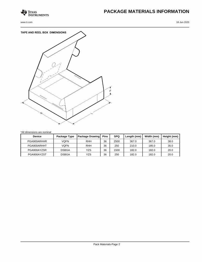
Device Package Type Package Drawing Pins SPQ Length (mm) Width (mm) Height (mm)
PGA900ARHHR VQFN RHH 36 2500 367.0 367.0 38.0
PGA900ARHHT VQFN RHH 36 250 210.0 185.0 35.0
PGA900AYZSR DSBGA YZS 36 1500 182.0 182.0 20.0
PGA900AYZST DSBGA YZS 36 250 182.0 182.0 20.0
PACKAGE MATERIALS INFORMATION
www.ti.com 18-Jun-2020
Pack Materials-Page 2

www.ti.com
GENERIC PACKAGE VIEW
This image is a representation of the package family, actual package may vary.Refer to the product data sheet for package details.
VQFN - 1 mm max heightRHH 36PLASTIC QUAD FLATPACK - NO LEAD6 x 6, 0.5 mm pitch
4225440/A

www.ti.com
PACKAGE OUTLINE
6.15.9
6.15.9
1.00.8
0.050.00
2X 4
32X 0.5
2X 4
36X 0.650.45
36X 0.300.18
4.4 0.1
(0.2) TYP
VQFN - 1 mm max heightRHH0036CPLASTIC QUAD FLATPACK - NO LEAD
4225412/A 10/2019
0.08 C
0.1 C A B0.05
NOTES: 1. All linear dimensions are in millimeters. Any dimensions in parenthesis are for reference only. Dimensioning and tolerancing per ASME Y14.5M. 2. This drawing is subject to change without notice. 3. The package thermal pad must be soldered to the printed circuit board for thermal and mechanical performance.
PIN 1 INDEX AREA
SEATING PLANE
PIN 1 ID
SYMMEXPOSED
THERMAL PAD
SYMM
1
9
10 18
19
27
2836
37
SCALE 2.300
AB
C

www.ti.com
EXAMPLE BOARD LAYOUT
32X (0.5)
(R0.05) TYP
0.07 MAXALL AROUND
0.07 MINALL AROUND
36X (0.75)
36X (0.24)
(5.65)
(5.65)
( 4.4)
( 0.2) TYPVIA
(1.12)TYP
(1.95)TYP
(1.12)TYP
(1.95) TYP
VQFN - 1 mm max heightRHH0036CPLASTIC QUAD FLATPACK - NO LEAD
4225412/A 10/2019
NOTES: (continued) 4. This package is designed to be soldered to a thermal pad on the board. For more information, see Texas Instruments literature number SLUA271 (www.ti.com/lit/slua271).5. Vias are optional depending on application, refer to device data sheet. If any vias are implemented, refer to their locations shown on this view. It is recommended that vias under paste be filled, plugged or tented.
SYMM
SYMM
LAND PATTERN EXAMPLEEXPOSED METAL SHOWN
SCALE: 15X
SEE SOLDER MASKDETAIL
1
9
10 18
19
27
2836
37
METAL EDGE
SOLDER MASKOPENING
EXPOSEDMETAL
METAL UNDERSOLDER MASK
SOLDER MASKOPENING
EXPOSEDMETAL
NON SOLDER MASKDEFINED
(PREFERRED)SOLDER MASK DEFINED
SOLDER MASK DETAILS

www.ti.com
EXAMPLE STENCIL DESIGN
36X (0.75)
36X (0.24)
32X (0.5)
(5.65)
(5.65)
16X ( 0.92)
(R0.05) TYP
(0.56) TYP
(1.12) TYP
(0.56)TYP
(1.12)TYP
VQFN - 1 mm max heightRHH0036CPLASTIC QUAD FLATPACK - NO LEAD
4225412/A 10/2019
NOTES: (continued) 6. Laser cutting apertures with trapezoidal walls and rounded corners may offer better paste release. IPC-7525 may have alternate design recommendations.
SOLDER PASTE EXAMPLEBASED ON 0.125 MM THICK STENCIL
SCALE: 15X
EXPOSED PAD 3770% PRINTED SOLDER COVERAGE BY AREA UNDER PACKAGE
SYMM
SYMM
1
9
10 18
19
27
2836
37

www.ti.com
PACKAGE OUTLINE
C0.625 MAX
0.2250.175
2.5TYP
2.5TYP
0.5 TYP
0.5 TYP
36X 0.30.2
B E A
D
4219444/A 02/2018
DSBGA - 0.625 mm max heightYZS0036DIE SIZE BALL GRID ARRAY
NOTES: 1. All linear dimensions are in millimeters. Any dimensions in parenthesis are for reference only. Dimensioning and tolerancing per ASME Y14.5M.2. This drawing is subject to change without notice.
BALL A1CORNER
SEATING PLANEBALL TYP 0.05 C
A
1 2 3
0.015 C A B
4 5 6
SYMM
SYMM
B
C
D
E
F
SCALE 5.000
D: Max =
E: Max =
3.745 mm, Min =
3.62 mm, Min =
3.685 mm
3.56 mm
www.ti.com
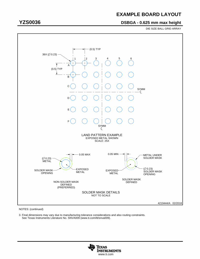
EXAMPLE BOARD LAYOUT
0.05 MIN0.05 MAX
36X ( 0.23)
(0.5) TYP
(0.5) TYP
( 0.23)SOLDER MASKOPENING
( 0.23)METAL
4219444/A 02/2018
DSBGA - 0.625 mm max heightYZS0036DIE SIZE BALL GRID ARRAY
NOTES: (continued) 3. Final dimensions may vary due to manufacturing tolerance considerations and also routing constraints. See Texas Instruments Literature No. SNVA009 (www.ti.com/lit/snva009).
SOLDER MASK DETAILSNOT TO SCALE
SYMM
SYMM
C
1 2 3 4 5 6
A
B
D
E
F
LAND PATTERN EXAMPLEEXPOSED METAL SHOWN
SCALE: 25X
NON-SOLDER MASKDEFINED
(PREFERRED)
EXPOSEDMETAL
SOLDER MASKOPENING
SOLDER MASKDEFINED
METAL UNDERSOLDER MASK
EXPOSEDMETAL

www.ti.com
EXAMPLE STENCIL DESIGN
(0.5) TYP
(0.5) TYP
36X ( 0.25) (R0.05) TYP
4219444/A 02/2018
DSBGA - 0.625 mm max heightYZS0036DIE SIZE BALL GRID ARRAY
NOTES: (continued) 4. Laser cutting apertures with trapezoidal walls and rounded corners may offer better paste release.
SYMM
SYMM
1 2 3 4 5 6
C
A
B
D
E
F
SOLDER PASTE EXAMPLEBASED ON 0.1 mm THICK STENCIL
SCALE: 25X
METALTYP

IMPORTANT NOTICE AND DISCLAIMERTI PROVIDES TECHNICAL AND RELIABILITY DATA (INCLUDING DATASHEETS), DESIGN RESOURCES (INCLUDING REFERENCEDESIGNS), APPLICATION OR OTHER DESIGN ADVICE, WEB TOOLS, SAFETY INFORMATION, AND OTHER RESOURCES “AS IS”AND WITH ALL FAULTS, AND DISCLAIMS ALL WARRANTIES, EXPRESS AND IMPLIED, INCLUDING WITHOUT LIMITATION ANYIMPLIED WARRANTIES OF MERCHANTABILITY, FITNESS FOR A PARTICULAR PURPOSE OR NON-INFRINGEMENT OF THIRDPARTY INTELLECTUAL PROPERTY RIGHTS.These resources are intended for skilled developers designing with TI products. You are solely responsible for (1) selecting the appropriateTI products for your application, (2) designing, validating and testing your application, and (3) ensuring your application meets applicablestandards, and any other safety, security, or other requirements. These resources are subject to change without notice. TI grants youpermission to use these resources only for development of an application that uses the TI products described in the resource. Otherreproduction and display of these resources is prohibited. No license is granted to any other TI intellectual property right or to any third partyintellectual property right. TI disclaims responsibility for, and you will fully indemnify TI and its representatives against, any claims, damages,costs, losses, and liabilities arising out of your use of these resources.TI’s products are provided subject to TI’s Terms of Sale (https:www.ti.com/legal/termsofsale.html) or other applicable terms available eitheron ti.com or provided in conjunction with such TI products. TI’s provision of these resources does not expand or otherwise alter TI’sapplicable warranties or warranty disclaimers for TI products.IMPORTANT NOTICE
Mailing Address: Texas Instruments, Post Office Box 655303, Dallas, Texas 75265Copyright © 2021, Texas Instruments Incorporated