Embed Size (px)
Citation preview
PHYSICAL REVIEW B 86, 094509 (2012)
Phase-sensitive evidence for dx2− y2-pairing symmetry in the parent-structure high-Tc cupratesuperconductor Sr1−xLaxCuO2
Jochen Tomaschko,1 Sebastian Scharinger,1 Victor Leca,1,2 Joachim Nagel,1 Matthias Kemmler,1 Teresa Selistrovski,1
Dieter Koelle,1 and Reinhold Kleiner1,*
1Physikalisches Institut–Experimentalphysik II and Center for Collective Quantum Phenomena in LISA+, Universitat Tubingen, Auf derMorgenstelle 14, 72076 Tubingen, Germany
2National Institute for Research and Development in Microtechnologies, Molecular Nanotechnology Laboratory, Erou Iancu Nicolae Street126A, RO-077190, Bucharest, Romania
(Received 23 March 2012; published 7 September 2012)
We report on a phase sensitive study of the superconducting order parameter of the infinite layer cuprateSr1−xLaxCuO2 (SLCO), with x ≈ 0.15. For the study a SLCO thin film was grown epitaxially on a tetracrystalsubstrate and patterned into direct-current superconducting quantum interference devices (dc SQUIDs). Thegeometry was designed to be frustrated for dx2−y2 -wave pairing, that is, the SQUID ring comprising the tetracrystalpoint contains one 0 Josephson junction and one π Josephson junction, if the order parameter has dx2−y2 -wavesymmetry. Our results show that SLCO indeed is a dx2−y2 -wave superconductor. This symmetry thus seems tobe inherent to cuprate superconductivity. Subdominant order parameter components can be ruled out at least ona 5% level and may not be a necessary ingredient of high-Tc superconductivity.
DOI: 10.1103/PhysRevB.86.094509 PACS number(s): 74.72.Ek, 74.20.Rp, 74.50.+r, 85.25.Dq
I. INTRODUCTION
Since the discovery of high transition temperature (high-Tc) superconductivity in cuprates,1 tremendous work hasbeen performed on these materials. Researchers succeededin increasing Tc from initially 30 to 135 K2–4 by synthesizingincreasingly complex compounds. All these materials havein common that superconductivity resides in the copper oxide(CuO2) planes where superconducting charge carriers, Cooperpairs, form. An “infinite layer” (IL) cuprate consisting essen-tially of CuO2 planes is therefore of fundamental interest for allquestions addressing the basics of high-Tc superconductivity,for example, in view of the still unknown pairing mechanism,which is one of the most important unsolved issues incondensed matter physics. In 1988, Siegrist et al. succeededin synthesizing such a simple cuprate, which is also known asthe “parent structure” of cuprate superconductors.5 Its CuO2
planes are only separated by a single alkaline earth metal plane(A = Ca, Sr or Ba), forming a ACuO2 crystal. Upon electrondoping, it turned out to be superconducting with maximumTc = 43 K.6–9
In contrast to conventional superconductors the high-Tc
cuprates are low-dimensional doped Mott insulators withstrongly correlated electrons or holes as charge carriers. Thecuprates exhibit many unusual and often not well understoodproperties both in their normal state and superconducting state,like the appearance of a pseudogap or the (unconventional)symmetry of the superconducting order parameter.10–12 Dueto their exceptionally simple structure, IL compounds couldplay a decisive role in resolving some of these issues, thuscontributing to the general physics of strongly correlatedelectron systems. In the following we focus on the symmetry ofthe superconducting order parameter. For hole-doped cupratesdx2−y2 -wave pairing is established.13–15 Also, the electron-doped T ′ compounds16 L2−xCexCuO4 (L = La, Pr, Nd, Eu, orSm) have been shown to be predominant dx2−y2 -wave super-conductors by a number of phase-sensitive experiments.17–20
Strikingly, for the parent compounds the pairing symmetry is
essentially still unknown since a variety of experimental testsyielded conflicting results.16,21–30
Phase-sensitive tests, such as experiments on cornerjunctions,31 tricrystal rings,32 or tetracrystal SQUIDs,18,33,34
are widely recognized to provide clear evidence for the pairingsymmetry of the order parameter.15 Such experiments rely onJosephson junctions, which for IL cuprate thin films becameavailable only very recently.35 Here we report on phase sensi-tive experiments on the IL compound Sr1−xLaxCuO2 (SLCO),using tetracrystal dc SQUIDs. Our data unambiguously showthat SLCO has dx2−y2 -wave symmetry which thus seems to beuniversal for the cuprate superconductors.
II. SAMPLE DESIGN AND FABRICATION
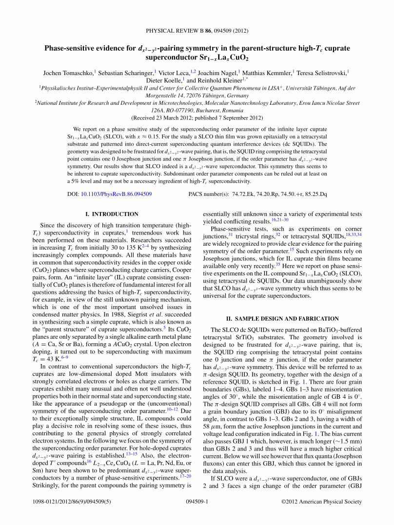
The SLCO dc SQUIDs were patterned on BaTiO3-bufferedtetracrystal SrTiO3 substrates. The geometry involved isdesigned to be frustrated for dx2−y2 -wave pairing, that is,the SQUID ring comprising the tetracrystal point containsone 0 junction and one π junction, if the order parameterhas dx2−y2 -wave symmetry. This device will be referred to asπ -design SQUID. Its geometry, together with the design of areference SQUID, is sketched in Fig. 1. There are four grainboundaries (GBs), labeled 1–4. GBs 1–3 have misorientationangles of 30, while the misorientation angle of GB 4 is 0.The π -design SQUID comprises all GBs. GB 4 will not forma grain boundary junction (GBJ) due to its 0 misalignmentangle, in contrast to GBs 1–3. GBs 2 and 3, having a width of58 μm, form the active Josephson junctions in the current andvoltage lead configuration indicated in Fig. 1. The bias currentalso passes GBJ 1 which, however, is much longer (∼1.5 mm)than GBJs 2 and 3 and thus will have a much higher criticalcurrent. Below we will see however that flux quanta (Josephsonfluxons) can enter this GBJ, which thus cannot be ignored inthe data analysis.
If SLCO were a dx2−y2 -wave superconductor, one of GBJs2 and 3 faces a sign change of the order parameter (GBJ
094509-11098-0121/2012/86(9)/094509(5) ©2012 American Physical Society
JOCHEN TOMASCHKO et al. PHYSICAL REVIEW B 86, 094509 (2012)
voltage relative to the unperturbed value of V . In a similarway, Abrikosov vortices trapped in a YBa2Cu3O7 SQUID,41
as well as Josephson fluxons having entered a GBJ,42 havebeen imaged by LTSEM.
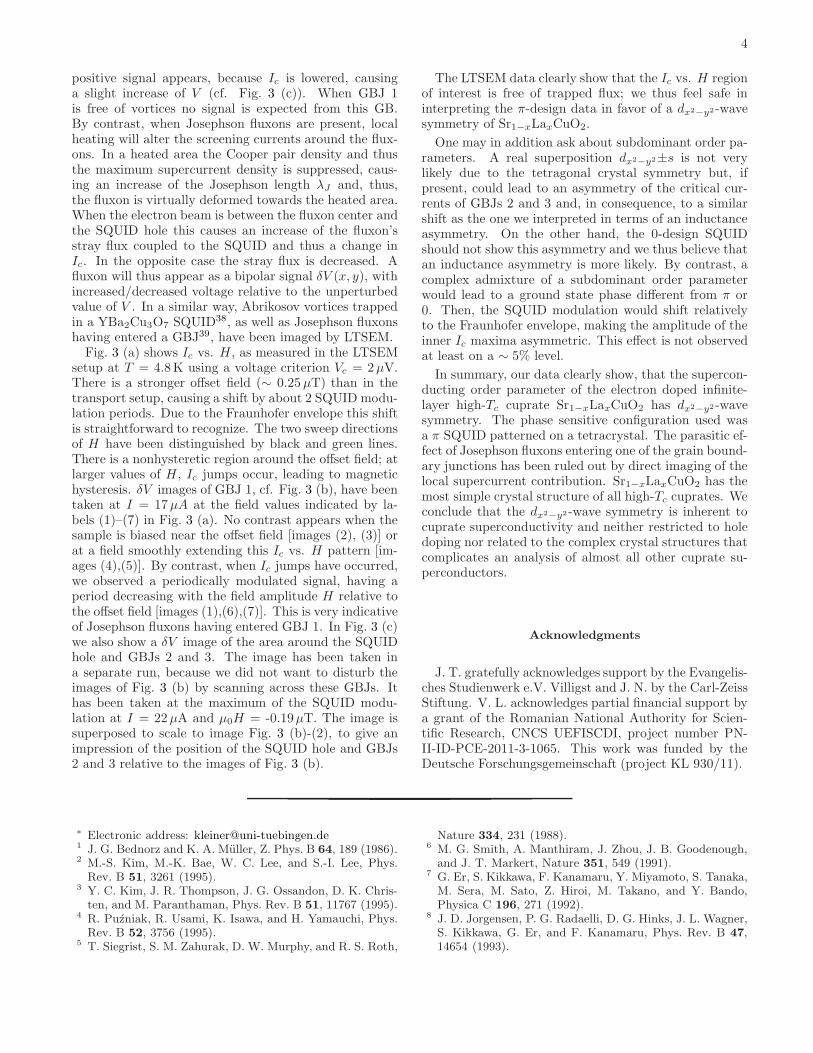
Figure 3(a) shows Ic vs H , as measured in the LTSEMsetup at T = 4.8 K using a voltage criterion Vc = 2 μV. Thereis a stronger offset field (∼0.25 μT) than in the transportsetup, causing a shift by about 2 SQUID modulation periods.Due to the Fraunhofer envelope this shift is straightforwardto recognize. The two sweep directions of H have beendistinguished by black and green lines. There is a nonhystereticregion around the offset field; at larger values of H , Ic jumpsoccur, leading to magnetic hysteresis. δV images of GBJ 1[cf. Fig. 3(b)] have been taken at I = 17 μA at the fieldvalues indicated by labels (1)–(7) in Fig. 3(a). No contrastappears when the sample is biased near the offset field [images(2) and (3)] or at a field smoothly extending this Ic vs H
pattern [images (4) and (5)]. By contrast, when Ic jumps haveoccurred, we observed a periodically modulated signal, havinga period decreasing with the field amplitude H relative to theoffset field [images (1), (6), and (7)]. This is very indicative ofJosephson fluxons having entered GBJ 1. In Fig. 3(c) we alsoshow a δV image of the area around the SQUID hole and GBJs2 and 3. The image has been taken in a separate run becausewe did not want to disturb the images of Fig. 3(b) by scanningacross these GBJs. It has been taken at the maximum of theSQUID modulation at I = 22 μA and μ0H = −0.19 μT. Theimage is superposed to scale to image Fig. 3(b)-(2), to give animpression of the position of the SQUID hole and GBJs 2 and3 relative to the images of Fig. 3(b).
The LTSEM data clearly show that the Ic vs H region ofinterest is free of trapped flux; we thus feel safe in interpretingthe π -design data in favor of a dx2−y2 -wave symmetry ofSr1−xLaxCuO2.
VI. DISCUSSION OF SUBDOMINANT ORDERPARAMETERS
One may in addition ask about subdominant order param-eters. A real superposition dx2−y2±s is not very likely due tothe tetragonal crystal symmetry but, if present, could lead to
an asymmetry of the critical currents of GBJs 2 and 3 and,in consequence, to a similar shift as the one we interpretedin terms of an inductance asymmetry. On the other hand,the 0-design SQUID should not show this asymmetry andwe thus believe that an inductance asymmetry is more likely.By contrast, a complex admixture of a subdominant orderparameter would lead to a ground state phase different fromπ or 0. Then, the SQUID modulation would shift relatively tothe Fraunhofer envelope, making the amplitude of the inner Ic
maxima asymmetric. This effect is not observed at least on a∼5% level.
VII. CONCLUSIONS
In summary, our data clearly show that the supercon-ducting order parameter of the infinite-layer high-Tc cuprateSr1−xLaxCuO2 has dx2−y2 -wave symmetry. The phase sen-sitive configuration used was a π SQUID patterned on atetracrystal. The parasitic effect of Josephson fluxons enteringone of the grain boundary junctions has been ruled out by directimaging of the local supercurrent distribution. Sr1−xLaxCuO2
has the most simple crystal structure of all high-Tc cuprates. Weconclude that the dx2−y2 -wave symmetry is inherent to cupratesuperconductivity and neither restricted to hole doping norrelated to the complex crystal structures that complicates ananalysis of almost all other cuprate superconductors. Such auniversal behavior is, for example, expected if Cooper pairingis mediated by antiferromagnetic spin fluctuations13,43 or inthe recently proposed fluctuating Cu-O-Cu bond model.44,45
Subdominant order parameters are absent at least on a 5%level and may not be a necessary ingredient of high-Tc
superconductivity.
ACKNOWLEDGMENTS
J.T. gratefully acknowledges support by the EvangelischesStudienwerk e.V. Villigst and J.N. by the Carl-Zeiss Stiftung.V.L. acknowledges partial financial support by a grant of theRomanian National Authority for Scientific Research, CNCSUEFISCDI, project number PN-II-ID-PCE-2011-3-1065. Thiswork was funded by the Deutsche Forschungsgemeinschaft(project KL 930/11).
*[email protected]. G. Bednorz and K. A. Muller, Z. Phys. B 64, 189(1986).
2M.-S. Kim, M.-K. Bae, W. C. Lee, and S.-I. Lee, Phys. Rev. B 51,3261 (1995).
3Y. C. Kim, J. R. Thompson, J. G. Ossandon, D. K. Christen, andM. Paranthaman, Phys. Rev. B 51, 11767 (1995).
4R. Puzniak, R. Usami, K. Isawa, and H. Yamauchi, Phys. Rev. B52, 3756 (1995).
5T. Siegrist, S. M. Zahurak, D. W. Murphy, and R. S. Roth, Nature(London) 334, 231 (1988).
6M. G. Smith, A. Manthiram, J. Zhou, J. B. Goodenough, and J. T.Markert, Nature (London) 351, 549 (1991).
7G. Er, S. Kikkawa, F. Kanamaru, Y. Miyamoto, S. Tanaka, M. Sera,M. Sato, Z. Hiroi, M. Takano, and Y. Bando, Physica C 196, 271(1992).
8J. D. Jorgensen, P. G. Radaelli, D. G. Hinks, J. L. Wagner,S. Kikkawa, G. Er, and F. Kanamaru, Phys. Rev. B 47, 14654(1993).
9N. Ikeda, Z. Hiroi, M. Azuma, M. Takano, Y. Bando, and Y. Takeda,Physica C 210, 367 (1993).
10M. R. Norman and C. Pepin, Rep. Prog. Phys. 66, 1547 (2003).11D. A. Bonn, Nat. Phys. 2, 159 (2006).12P. A. Lee, Rep. Prog. Phys. 71, 012501 (2008).13D. J. Scalapino, Phys. Rep. 250, 329 (1995).14D. J. V. Harlingen, Rev. Mod. Phys. 67, 515 (1995).
094509-4
arX
iv:1
203.
5237
v1 [
cond
-mat
.sup
r-co
n] 2
3 M
ar 2
012
Phase-sensitive evidence for dx2−y2 - pairing symmetry in the
parent-structure high-Tc cuprate superconductor Sr1−xLaxCuO2
J. Tomaschko,1 S. Scharinger,1 V. Leca,1, 2 J. Nagel,1 M. Kemmler,1 T. Selistrovski,1 D. Koelle,1 and R. Kleiner1, ∗
1Physikalisches Institut – Experimentalphysik II and Center for Collective Quantum Phenomena in LISA+,
Universitat Tubingen, Auf der Morgenstelle 14, 72076 Tubingen, Germany2National Institute for Research and Development in Microtechnologies,
Molecular Nanotechnology Laboratory, Erou Iancu Nicolae Str. 126A, RO-077190, Bucharest, Romania
(Dated: March 26, 2012)
Even after 25 years of research the pairing mechanism and – at least for electron doped com-pounds – also the order parameter symmetry of the high transition temperature (high-Tc) cupratesuperconductors is still under debate. One of the reasons is the complex crystal structure of mostof these materials. An exception are the infinite layer (IL) compounds consisting essentially ofCuO2 planes. Unfortunately, these materials are difficult to grow and, thus, there are only fewexperimental investigations. Recently, we succeeded in depositing high quality films of the electrondoped IL compound Sr1−xLaxCuO2 (SLCO), with x ≈ 0.15, and on the fabrication of well-definedgrain boundary Josephson junctions (GBJs) based on such SLCO films. Here we report on a phasesensitive study of the superconducting order parameter based on GBJ SQUIDs from a SLCO filmgrown on a tetracrystal substrate. Our results show that also the parent structure of the high-Tc
cuprates has dx2−y2 -wave symmetry, which thus seems to be inherent to cuprate superconductivity.
PACS numbers: 74.50.+r, 74.72.-h, 74.72.Ek, 85.25.Dq
Since the discovery of high transition temperature(high-Tc) superconductivity in cuprates1, tremendouswork has been performed on these materials. Researcherssucceeded in increasing Tc from initially 30K to 135K2–4
by synthesizing increasingly complex compounds. How-ever, the microscopic mechanism causing high-Tc super-conductivity still has not been identified and is one ofthe biggest issues in solid state physics. All these ma-terials have in common that superconductivity residesin the copper oxide (CuO2) planes where superconduct-ing charge carriers, Cooper pairs, form. An “infinitelayer” (IL) cuprate consisting essentially of CuO2 planesis therefore of fundamental interest for all questions ad-dressing the basics of high-Tc superconductivity. In 1988,Siegrist et al. succeeded in synthesizing such a simplecuprate, which is known as the “parent structure” ofcuprate superconductors5. Its CuO2 planes are only sep-arated by a single alkaline earth metal plane (A = Ca,Sr or Ba), forming a ACuO2 crystal. Upon electron-doping, it turned out to be superconducting with maxi-mum Tc = 43K6–9.
A striking and highly debated feature of the cupratesuperconductors is their unconventional order parame-ter symmetry. Whereas for hole-doped cuprates dx2
−y2 -wave pairing has been established10–12, for electron-doped cuprates13 the issue is not yet completely set-tled. After controversial discussion, the electron-dopedT ′-compounds L2−xCexCuO4 (L = La, Pr, Nd, Euor Sm) have been shown to be predominant dx2
−y2 -wave superconductors by a number of phase-sensitiveexperiments14–17. By contrast, for the parent com-pounds the pairing symmetry is essentially still unknown,since a variety of experimental tests yielded conflictingresults13,18–27. Phase-sensitive tests, such as experimentson corner junctions28, tricrystal rings29 or tetracrys-
tal SQUIDs15,30,31, are widely recognized to provide aclear evidence for the pairing symmetry of the orderparameter12. Such experiments rely on Josephson junc-tions, which for IL cuprate thin films became availableonly very recently32.
Here we report on the fabrication and characterizationof thin-film Sr1−xLaxCuO2 (SLCO) dc SQUIDs basedon BaTiO3-buffered tetracrystal SrTiO3 substrates. Thegeometry involved is designed to be frustrated fordx2
−y2-wave pairing, i.e. the SQUID ring comprising thetetracrystal point contains one 0 junction and one π junc-tion, if the order parameter has dx2
−y2-wave symmetry.This device will be referred to as π-design SQUID. Its ge-ometry, together with the design of a reference SQUID,is sketched in Fig. 1. There are four grain boundaries(GBs), labelled 1–4. GBs 1–3 have misorientation an-gles of 30, while the misorientation angle of GB 4 is0. The π-design SQUID comprises all GBs. GB 4 willnot form a grain boundary junction (GBJ) due to its 0
misalignment angle, in contrast to GBs 1–3. GBs 2 and3, having a width of 58µm, form the active Josephsonjunctions in the current and voltage lead configurationindicated in Fig. 1. The bias current also passes GBJ 1which, however, is much longer (∼1.5mm) than GBJs 2and 3 and thus will have a much higher critical current.Below, we will see however, that flux quanta (Joseph-son fluxons) can enter this GBJ, which thus cannot beignored in the data analysis. If SLCO is a dx2
−y2-wavesuperconductor, one of GBJs 2 and 3 faces a sign changeof the order parameter (GBJ 3 in Fig. 1), thus forming aπ Josephson junction. The other GBJs are conventional.The area of GBJs 2 and 3 is not much smaller than thearea of the SQUID hole. In this “spatially distributedjunction” design33 the junction’s Ic vs. H modulation(Fraunhofer pattern) is superposed on the SQUID mod-
2
V
V
V
V
I
I
I
I
0
0
0
V
V
I
0
0
0
ba
a
15°
45°
b
b
a
15°
a
45°
b
0
0 design
design
1
2
4
3
H
Imod
FIG. 1: (Color online) Schematic layout of the SQUIDs. The0-design SQUID comprises two conventional GBJs (0 junc-tions) straddling a single 30 [001]-tilt grain boundary. Theπ-design SQUID comprises four GBs. The misorientation an-gle of GB 4 is 0. All other misorientation angles are 30.The dx2
−y2 -wave order parameter is indicated by the clover-leaf structure consisting of white and black lobes, indicatingthe sign change of the order parameter. Leads for bias cur-rent I and voltage V are indicated. In some experiments, forthe π-design SQUID we have also sent a current Imod acrossGB 1. Magnetic fields have been applied perpendicular to thesubstrate plane.
ulation on a similar field scale. The (a)symmetry of theSQUID modulation relative to the Fraunhofer envelopeallows to detect residual fields and often also trappedmagnetic flux.
The reference SQUIDs – there were two referenceSQUIDs, producing very similar results – cross only oneof the 30 GBs and incorporate two 50µm wide GBJs,which act as conventional junctions both for s-wave anddx2−y2-wave order parameters. Below, these devices willbe referred to as the 0-design SQUIDs. Both the π-design SQUID and the reference SQUIDs had rectangularSQUID holes with an area AS = 50× 75µm2.
The samples have been fabricated by pulsed laser de-position, as described elsewhere32,34,35. In brief, we firstdeposited a 25 nm thick BaTiO3 thin-film on the SrTiO3
tetracystal, acting as a buffer layer. This layer was fol-lowed by a 22 nm thick SLCO thin-film, with dopingx ≈ 0.15. Finally, a 10 nm thick gold layer was evap-orated in-situ, protecting SLCO from degradation andacting as resistive shunt for the GBJs. The SQUIDswere patterned by standard photolithography and argon
ion milling. The SLCO film had a critical temperatureTc ≈ 18K. Electric transport measurements were per-formed at T = 4.2K in a four-point configuration, withthe sample mounted inside a noise-filtered, magneticallyand radio frequency shielded probe in a liquid-helium de-war. A SQUID amplifier was used to allow for low-noisemeasurements.
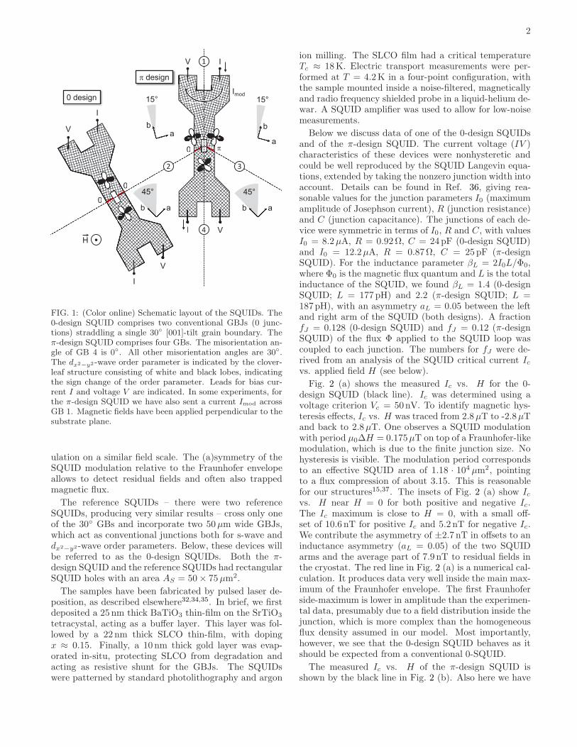
Below we discuss data of one of the 0-design SQUIDsand of the π-design SQUID. The current voltage (IV )characteristics of these devices were nonhysteretic andcould be well reproduced by the SQUID Langevin equa-tions, extended by taking the nonzero junction width intoaccount. Details can be found in Ref. 36, giving rea-sonable values for the junction parameters I0 (maximumamplitude of Josephson current), R (junction resistance)and C (junction capacitance). The junctions of each de-vice were symmetric in terms of I0, R and C, with valuesI0 = 8.2µA, R = 0.92Ω, C = 24pF (0-design SQUID)and I0 = 12.2µA, R = 0.87Ω, C = 25pF (π-designSQUID). For the inductance parameter βL = 2I0L/Φ0,where Φ0 is the magnetic flux quantum and L is the totalinductance of the SQUID, we found βL = 1.4 (0-designSQUID; L = 177pH) and 2.2 (π-design SQUID; L =187pH), with an asymmetry aL = 0.05 between the leftand right arm of the SQUID (both designs). A fractionfJ = 0.128 (0-design SQUID) and fJ = 0.12 (π-designSQUID) of the flux Φ applied to the SQUID loop wascoupled to each junction. The numbers for fJ were de-rived from an analysis of the SQUID critical current Icvs. applied field H (see below).
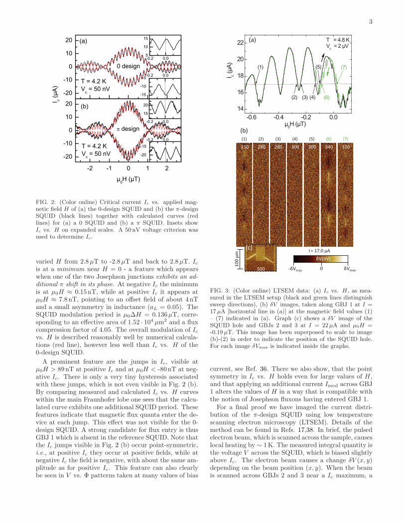
Fig. 2 (a) shows the measured Ic vs. H for the 0-design SQUID (black line). Ic was determined using avoltage criterion Vc = 50nV. To identify magnetic hys-teresis effects, Ic vs. H was traced from 2.8µT to -2.8µTand back to 2.8µT. One observes a SQUID modulationwith period µ0∆H = 0.175µT on top of a Fraunhofer-likemodulation, which is due to the finite junction size. Nohysteresis is visible. The modulation period correspondsto an effective SQUID area of 1.18 · 104 µm2, pointingto a flux compression of about 3.15. This is reasonablefor our structures15,37. The insets of Fig. 2 (a) show Icvs. H near H = 0 for both positive and negative Ic.The Ic maximum is close to H = 0, with a small off-set of 10.6 nT for positive Ic and 5.2 nT for negative Ic.We contribute the asymmetry of ±2.7 nT in offsets to aninductance asymmetry (aL = 0.05) of the two SQUIDarms and the average part of 7.9 nT to residual fields inthe cryostat. The red line in Fig. 2 (a) is a numerical cal-culation. It produces data very well inside the main max-imum of the Fraunhofer envelope. The first Fraunhoferside-maximum is lower in amplitude than the experimen-tal data, presumably due to a field distribution inside thejunction, which is more complex than the homogeneousflux density assumed in our model. Most importantly,however, we see that the 0-design SQUID behaves as itshould be expected from a conventional 0-SQUID.
The measured Ic vs. H of the π-design SQUID isshown by the black line in Fig. 2 (b). Also here we have
3
-2 -1 0 1 2
-20
-10
0
10
20
-20
-10
0
10
20
I c (µA
)
µ0H (µT)
(b)
design
T = 4.2 KVc = 50 nV
T = 4.2 KVc = 50 nV
(a)
0 design
-0.2 0.05
10
15
-15
-10
-5-0.2 0.0
-0.2 0.0
15
20
-20
-15-0.2 0.0
FIG. 2: (Color online) Critical current Ic vs. applied mag-netic field H of (a) the 0-design SQUID and (b) the π-designSQUID (black lines) together with calculated curves (redlines) for (a) a 0 SQUID and (b) a π SQUID. Insets showIc vs. H on expanded scales. A 50 nV voltage criterion wasused to determine Ic.
varied H from 2.8µT to -2.8µT and back to 2.8µT. Icis at a minimum near H = 0 - a feature which appearswhen one of the two Josephson junctions exhibits an ad-
ditional π shift in its phase. At negative Ic the minimumis at µ0H ≈ 0.15nT, while at positive Ic it appears atµ0H ≈ 7.8 nT, pointing to an offset field of about 4 nTand a small asymmetry in inductance (aL = 0.05). TheSQUID modulation period is µ0∆H = 0.136µT, corre-sponding to an effective area of 1.52 · 104 µm2 and a fluxcompression factor of 4.05. The overall modulation of Icvs. H is described reasonably well by numerical calcula-tions (red line), however less well than Ic vs. H of the0-design SQUID.
A prominent feature are the jumps in Ic, visible atµ0H > 89 nT at positive Ic and at µ0H < -80nT at neg-ative Ic. There is only a very tiny hysteresis associatedwith these jumps, which is not even visible in Fig. 2 (b).By comparing measured and calculated Ic vs. H curveswithin the main Fraunhofer lobe one sees that the calcu-lated curve exhibits one additional SQUID period. Thesefeatures indicate that magnetic flux quanta enter the de-vice at each jump. This effect was not visible for the 0-design SQUID. A strong candidate for flux entry is thusGBJ 1 which is absent in the reference SQUID. Note thatthe Ic jumps visible in Fig. 2 (b) occur point-symmetric,i.e., at positive Ic they occur at positive fields, while atnegative Ic the field is negative, with about the same am-plitude as for positive Ic. This feature can also clearlybe seen in V vs. Φ patterns taken at many values of bias
(6) (5) (4) (3) (2) (1)
Vmax
350 280 340 320
500
I = 17.0 µA
10
0 µ
m
(a)
(b)
(c)
- Vmax 0
V(nV)
(7)
300 300 280
-0.6 -0.4 -0.2 0.0
14
16
18
20
22
(1)
(2) (6)
(7)(5)
(4)
Ic (µ
A)
µ0H (µT)
(3)
T = 4.8 KV
c = 2 µV
FIG. 3: (Color online) LTSEM data: (a) Ic vs. H , as mea-sured in the LTSEM setup (black and green lines distinguishsweep directions), (b) δV images, taken along GBJ 1 at I =17µA [horizontal line in (a)] at the magnetic field values (1)– (7) indicated in (a). Graph (c) shows a δV image of theSQUID hole and GBJs 2 and 3 at I = 22µA and µ0H =-0.19µT. This image has been superposed to scale to image(b)-(2) in order to indicate the position of the SQUID hole.For each image δVmax is indicated inside the graphs.
current, see Ref. 36. There we also show, that the pointsymmetry in Ic vs. H holds even for large values of H ,and that applying an additional current Imod across GBJ1 alters the values of H in a way that is compatible withthe notion of Josephson fluxons having entered GBJ 1.For a final proof we have imaged the current distri-
bution of the π-design SQUID using low temperaturescanning electron microscopy (LTSEM). Details of themethod can be found in Refs. 17,38. In brief, the pulsedelectron beam, which is scanned across the sample, causeslocal heating by ∼ 1K. The measured integral quantity isthe voltage V across the SQUID, which is biased slightlyabove Ic. The electron beam causes a change δV (x, y)depending on the beam position (x, y). When the beamis scanned across GBJs 2 and 3 near a Ic maximum, a
4
positive signal appears, because Ic is lowered, causinga slight increase of V (cf. Fig. 3 (c)). When GBJ 1is free of vortices no signal is expected from this GB.By contrast, when Josephson fluxons are present, localheating will alter the screening currents around the flux-ons. In a heated area the Cooper pair density and thusthe maximum supercurrent density is suppressed, caus-ing an increase of the Josephson length λJ and, thus,the fluxon is virtually deformed towards the heated area.When the electron beam is between the fluxon center andthe SQUID hole this causes an increase of the fluxon’sstray flux coupled to the SQUID and thus a change inIc. In the opposite case the stray flux is decreased. Afluxon will thus appear as a bipolar signal δV (x, y), withincreased/decreased voltage relative to the unperturbedvalue of V . In a similar way, Abrikosov vortices trappedin a YBa2Cu3O7 SQUID38, as well as Josephson fluxonshaving entered a GBJ39, have been imaged by LTSEM.Fig. 3 (a) shows Ic vs. H , as measured in the LTSEM
setup at T = 4.8K using a voltage criterion Vc = 2µV.There is a stronger offset field (∼ 0.25µT) than in thetransport setup, causing a shift by about 2 SQUID modu-lation periods. Due to the Fraunhofer envelope this shiftis straightforward to recognize. The two sweep directionsof H have been distinguished by black and green lines.There is a nonhysteretic region around the offset field; atlarger values of H , Ic jumps occur, leading to magnetichysteresis. δV images of GBJ 1, cf. Fig. 3 (b), have beentaken at I = 17µA at the field values indicated by la-bels (1)–(7) in Fig. 3 (a). No contrast appears when thesample is biased near the offset field [images (2), (3)] orat a field smoothly extending this Ic vs. H pattern [im-ages (4),(5)]. By contrast, when Ic jumps have occurred,we observed a periodically modulated signal, having aperiod decreasing with the field amplitude H relative tothe offset field [images (1),(6),(7)]. This is very indicativeof Josephson fluxons having entered GBJ 1. In Fig. 3 (c)we also show a δV image of the area around the SQUIDhole and GBJs 2 and 3. The image has been taken ina separate run, because we did not want to disturb theimages of Fig. 3 (b) by scanning across these GBJs. Ithas been taken at the maximum of the SQUID modu-lation at I = 22µA and µ0H = -0.19µT. The image issuperposed to scale to image Fig. 3 (b)-(2), to give animpression of the position of the SQUID hole and GBJs2 and 3 relative to the images of Fig. 3 (b).
The LTSEM data clearly show that the Ic vs. H regionof interest is free of trapped flux; we thus feel safe ininterpreting the π-design data in favor of a dx2
−y2-wavesymmetry of Sr1−xLaxCuO2.
One may in addition ask about subdominant order pa-rameters. A real superposition dx2
−y2±s is not verylikely due to the tetragonal crystal symmetry but, ifpresent, could lead to an asymmetry of the critical cur-rents of GBJs 2 and 3 and, in consequence, to a similarshift as the one we interpreted in terms of an inductanceasymmetry. On the other hand, the 0-design SQUIDshould not show this asymmetry and we thus believe thatan inductance asymmetry is more likely. By contrast, acomplex admixture of a subdominant order parameterwould lead to a ground state phase different from π or0. Then, the SQUID modulation would shift relativelyto the Fraunhofer envelope, making the amplitude of theinner Ic maxima asymmetric. This effect is not observedat least on a ∼ 5% level.
In summary, our data clearly show, that the supercon-ducting order parameter of the electron doped infinite-layer high-Tc cuprate Sr1−xLaxCuO2 has dx2
−y2-wavesymmetry. The phase sensitive configuration used wasa π SQUID patterned on a tetracrystal. The parasitic ef-fect of Josephson fluxons entering one of the grain bound-ary junctions has been ruled out by direct imaging of thelocal supercurrent contribution. Sr1−xLaxCuO2 has themost simple crystal structure of all high-Tc cuprates. Weconclude that the dx2
−y2-wave symmetry is inherent tocuprate superconductivity and neither restricted to holedoping nor related to the complex crystal structures thatcomplicates an analysis of almost all other cuprate su-perconductors.
Acknowledgments
J. T. gratefully acknowledges support by the Evangelis-ches Studienwerk e.V. Villigst and J. N. by the Carl-ZeissStiftung. V. L. acknowledges partial financial support bya grant of the Romanian National Authority for Scien-tific Research, CNCS UEFISCDI, project number PN-II-ID-PCE-2011-3-1065. This work was funded by theDeutsche Forschungsgemeinschaft (project KL 930/11).
∗ Electronic address: [email protected] J. G. Bednorz and K. A. Muller, Z. Phys. B 64, 189 (1986).2 M.-S. Kim, M.-K. Bae, W. C. Lee, and S.-I. Lee, Phys.Rev. B 51, 3261 (1995).
3 Y. C. Kim, J. R. Thompson, J. G. Ossandon, D. K. Chris-ten, and M. Paranthaman, Phys. Rev. B 51, 11767 (1995).
4 R. Puzniak, R. Usami, K. Isawa, and H. Yamauchi, Phys.Rev. B 52, 3756 (1995).
5 T. Siegrist, S. M. Zahurak, D. W. Murphy, and R. S. Roth,
Nature 334, 231 (1988).6 M. G. Smith, A. Manthiram, J. Zhou, J. B. Goodenough,and J. T. Markert, Nature 351, 549 (1991).
7 G. Er, S. Kikkawa, F. Kanamaru, Y. Miyamoto, S. Tanaka,M. Sera, M. Sato, Z. Hiroi, M. Takano, and Y. Bando,Physica C 196, 271 (1992).
8 J. D. Jorgensen, P. G. Radaelli, D. G. Hinks, J. L. Wagner,S. Kikkawa, G. Er, and F. Kanamaru, Phys. Rev. B 47,14654 (1993).
5
9 N. Ikeda, Z. Hiroi, M. Azuma, M. Takano, Y. Bando, andY. Takeda, Physica C 210, 367 (1993).
10 D. J. Scalapino, Phys. Rep. 250, 329 (1995).11 D. J. V. Harlingen, Rev. Mod. Phys. 67, 515 (1995).12 C. C. Tsuei and J. R. Kirtley, Rev. Mod. Phys. 72, 969
(2000).13 N. P. Armitage, P. Fournier, and R. L. Greene, Rev. Mod.
Phys. 82, 2421 (2010).14 C. C. Tsuei and J. R. Kirtley, Phys. Rev. Lett. 85, 182
(2000).15 B. Chesca, K. Ehrhardt, M. Moßle, R. Straub, D. Koelle,
R. Kleiner, and A. Tsukada, Phys. Rev. Lett. 90, 057004(2003).
16 Ariando, D. Darminto, H.-J. H. Smilde, V. Leca, D. H. A.Blank, H. Rogalla, and H. Hilgenkamp, Phys. Rev. Lett.94, 167001 (2005).
17 C. Gurlich, E. Goldobin, R. Straub, D. Doenitz, Ariando,H.-J. H. Smilde, H. Hilgenkamp, R. Kleiner, and D. Koelle,Phys. Rev. Lett. 103, 067011 (2009).
18 T. Imai, C. P. Slichter, J. L. Cobb, and J. T. Markert, J.Phys. Chem. Solids 56, 1921 (1995).
19 C.-T. Chen, P. Seneor, N.-C. Yeh, R. P. Vasquez, L. D.Bell, C. U. Jung, J. Y. Kim, M.-S. Park, H.-J. Kim, andS.-I. Lee, Phys. Rev. Lett. 88, 227002 (2002).
20 G. V. M. Williams, R. Dupree, A. Howes, S. Kramer, H. J.Trodahl, C. U. Jung, M.-S. Park, and S.-I. Lee, Phys. Rev.B 65, 224520 (2002).
21 V. S. Zapf, N.-C. Yeh, A. D. Beyer, C. R. Hughes, C. H.Mielke, N. Harrison, M. S. Park, K. H. Kim, and S.-I. Lee,Phys. Rev. B 71, 134526 (2005).
22 Z. Y. Liu, H. H. Wen, L. Shan, H. P. Yang, X. F. Lu,H. Gao, M.-S. Park, C. U. Jung, and S.-I. Lee, Europhys.Lett. 69, 263 (2005).
23 K. H. Satoh, S. Takeshita, A. Koda, R. Kadono, K. Ishida,S. Pyon, T. Sasagawa, and H. Takagi, Phys. Rev. B 77,224503 (2008).
24 R. Khasanov, A. Shengelaya, A. Maisuradze, D. Di Castro,I. M. Savic, S. Weyeneth, M. S. Park, D. J. Jang, S.-I. Lee,and H. Keller, Phys. Rev. B 77, 184512 (2008).
25 J. S. White, E. M. Forgan, M. Laver, P. S. Hafliger,R. Khasanov, R. Cubitt, C. D. Dewhurst, M.-S. Park, D.-J. Jang, H.-G. Lee, et al., J. Phys.: Condens. Matter 20,104237 (2008).
26 M. L. Teague, A. D. Beyer, M. S. Grinolds, S. I. Lee, andN.-C. Yeh, Europhys. Lett. 85, 17004 (2009).
27 L. Fruchter, V. Jovanovic, H. Raffy, S. Labdi, F. Bouquet,and Z. Z. Li, Phys. Rev. B 82, 144529 (2010).
28 D. A. Wollman, D. J. Van Harlingen, W. C. Lee, D. M.Ginsberg, and A. J. Leggett, Phys. Rev. Lett. 71, 2134(1993).
29 C. C. Tsuei, J. R. Kirtley, C. C. Chi, L. Yu-Jahnes,A. Gupta, T. Shaw, J. Z. Sun, and M. B. Ketchen, Phys.Rev. Lett. 73, 593 (1994).
30 R. R. Schulz, B. Chesca, B. Goetz, C. W. Schnei-der, A. Schmehl, H. Bielefeldt, H. Hilgenkamp, andJ. Mannhart, Appl. Phys. Lett. 76, 912 (2000).
31 B. Chesca, R. R. Schulz, B. Goetz, C. W. Schneider,H. Hilgenkamp, and J. Mannhart, Phys. Rev. Lett. 88,177003 (2002).
32 J. Tomaschko, V. Leca, T. Selistrovski, R. Kleiner, andD. Koelle, Phys. Rev. B 84, 214507 (2011).
33 B. Chesca, Ann. Phys. 8, 511 (1999).34 J. Tomaschko, C. Raisch, V. Leca, T. Chasse, R. Kleiner,
and D. Koelle, Phys. Rev. B 84, 064521 (2011).35 J. Tomaschko, V. Leca, T. Selistrovski, S. Diebold,
J. Jochum, R. Kleiner, and D. Koelle, Phys. Rev. B 85,024519 (2012).
36 See supplementary material for additional transport data.37 M. B. Ketchen, W. J. Gallagher, A. W. Kleinsasser,
S. Murphy, and J. R. Clem, in SQUID 85, Superconduct-ing Quantum Interference Devices and Their Applications,Walter de Gruyter, Berlin, New York p. 865 (1985).
38 R. Straub, S. Keil, R. Kleiner, and D. Koelle, Appl. Phys.Lett. 78, 3645 (2001).
39 D. Koelle, R. Gross, R. Straub, S. Keil, M. Fischer,M. Peschka, R. P. Huebener, and K. Barthel, Physica C332, 148 (2000).
arX
iv:1
203.
5237
v1 [
cond
-mat
.sup
r-co
n] 2
3 M
ar 2
012
Supplementary information to
“Phase-sensitive evidence for dx2−y2 - pairing symmetry in the
parent-structure high-Tc cuprate superconductor Sr1−xLaxCuO2”
J. Tomaschko,1 S. Scharinger,1 V. Leca,1, 2 J. Nagel,1 M. Kemmler,1 T. Selistrovski,1 D. Koelle,1 and R. Kleiner1, ∗
1Physikalisches Institut – Experimentalphysik II and Center for Collective Quantum Phenomena in LISA+,
Universitat Tubingen, Auf der Morgenstelle 14, 72076 Tubingen, Germany2National Institute for Research and Development in Microtechnologies,
Molecular Nanotechnology Laboratory, Erou Iancu Nicolae Str. 126A, RO-077190, Bucharest, Romania
(Dated: March 26, 2012)
In this supplement we provide additional experimentaldata for the 0-design SQUID and the π-design SQUID:(I) current voltage (IV ) characteristics, (II) voltage Vvs. applied field H , (III) symmetry considerations onIc vs. H , and (IV) a measurement of the current stepheight caused by the SQUID LC resonances. Most mea-surements are accompanied by simulations. The modelequations are described in section I.
I. CURRENT VOLTAGE CHARACTERISTICS
AND MODEL
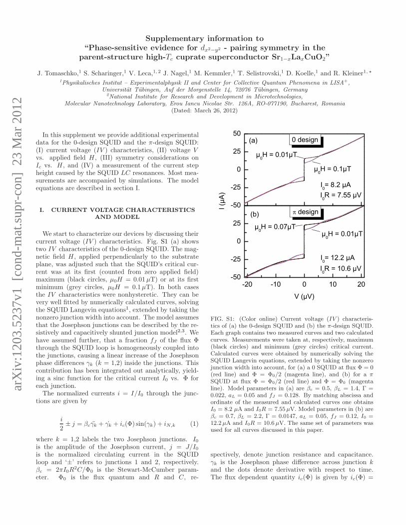
We start to characterize our devices by discussing theircurrent voltage (IV ) characteristics. Fig. S1 (a) showstwo IV characteristics of the 0-design SQUID. The mag-netic field H , applied perpendicularly to the substrateplane, was adjusted such that the SQUID’s critical cur-rent was at its first (counted from zero applied field)maximum (black circles, µ0H = 0.01µT) or at its firstminimum (grey circles, µ0H = 0.1µT). In both casesthe IV characteristics were nonhysteretic. They can bevery well fitted by numerically calculated curves, solvingthe SQUID Langevin equations1, extended by taking thenonzero junction width into account. The model assumesthat the Josephson junctions can be described by the re-sistively and capacitively shunted junction model2,3. Wehave assumed further, that a fraction fJ of the flux Φthrough the SQUID loop is homogeneously coupled intothe junctions, causing a linear increase of the Josephsonphase differences γk (k = 1,2) inside the junctions. Thiscontribution has been integrated out analytically, yield-ing a sinc function for the critical current I0 vs. Φ foreach junction.The normalized currents i = I/I0 through the junc-
tions are given by
i
2± j = βcγk + γk + ic(Φ) sin(γk) + iN,k (1)
where k = 1,2 labels the two Josephson junctions. I0is the amplitude of the Josephson current, j = J/I0is the normalized circulating current in the SQUIDloop and ‘±’ refers to junctions 1 and 2, respectively.βc = 2πI0R
2C/Φ0 is the Stewart-McCumber param-eter. Φ0 is the flux quantum and R and C, re-
-20 -10 0 10 20-50
-25
0
25
-50
-25
0
25
50
µ0H = 0.01µTµ0H = 0.07µT
I (µA
)
V (µV)
I0R = 10.6 µV
(b)
design
I0= 12.2 µA
µ0H = 0.1µT
µ0H = 0.01µT
I0= 8.2 µAI0R = 7.55 µV
(a)
0 design
FIG. S1: (Color online) Current voltage (IV ) characteris-tics of (a) the 0-design SQUID and (b) the π-design SQUID.Each graph contains two measured curves and two calculatedcurves. Measurements were taken at, respectively, maximum(black circles) and minimum (grey circles) critical current.Calculated curves were obtained by numerically solving theSQUID Langevin equations, extended by taking the nonzerojunction width into account, for (a) a 0 SQUID at flux Φ = 0(red line) and Φ = Φ0/2 (magenta line), and (b) for a π
SQUID at flux Φ = Φ0/2 (red line) and Φ = Φ0 (magentaline). Model parameters in (a) are βc = 0.5, βL = 1.4, Γ =0.022, aL = 0.05 and fJ = 0.128. By matching abscissa andordinate of the measured and calculated curves one obtainsI0 = 8.2 µA and I0R = 7.55µV. Model parameters in (b) areβc = 0.7, βL = 2.2, Γ = 0.0147, aL = 0.05, fJ = 0.12, I0 =12.2µA and I0R = 10.6 µV. The same set of parameters wasused for all curves discussed in this paper.
spectively, denote junction resistance and capacitance.γk is the Josephson phase difference across junction kand the dots denote derivative with respect to time.The flux dependent quantity ic(Φ) is given by ic(Φ) =
2
sin(πfJΦ/Φ0)/[πfJΦ/Φ0]. The normalized noise cur-rent iN,k has a spectral power density 4Γ, with Γ =2πkBT/I0Φ0. The above equations assumed that thejunction parameters βc and ic(Φ) are the same for bothjunctions. If junction k is a π junction, a phase π is tobe added to γk.The two phases γk are related by
γ2 − γ1 = 2πΦ/Φ0 + πβL(j + aLi) (2)
where βL = 2I0L/Φ0. L = L1+L2, where L1 and L2 arethe inductances of the two SQUID arms, related to theinductance asymmetry aL via Lk = L(1± aL)/2.From Eqs. (1) and (2) one obtains the normalized volt-
age v = V/I0R, and thus current voltage characteristics,critical current vs. flux etc., by taking the time averageof (γ1 + γ2)/2. A consistent set of model parameters canbe obtained by analyzing IV characteristics at maximumand minimum Ic, plus Ic vs. H .The calculated IV characteristics in Fig. S1 (a) are for
βc = 0.5, βL = 1.4, Γ = 0.022, aL = 0.05 and fJ = 0.128(the latter two numbers are actually determined from Icvs. H data). In dimensioned units one finds I0 = 8.2µAand I0R = 7.55µV, R = 0.92Ω, L = 177pH, C = 24pF.These are reasonable numbers for our SQUIDs. In theµ0H = 0.1µT curve of Fig. S1 (a) one also notices a humpfor 6µV < V < 10µV. This is a LC resonance, which be-comes maximally excited when the supercurrents acrossthe two junctions oscillate out-of-phase1.Two IV characteristics for the π-design SQUID are
shown in Fig. S1 (b). One first notices that the firstIc maximum (black circles) was obtained at a relativelylarge field, 0.07µT. By contrast, at µ0H = 0.01µT, Ichad a minimum (grey circles). Simulating these curves(red line for µ0H = 0.07µT and magenta line for µ0H =0.01 µT) we have assumed that junction 2 is a π junctionand further used the parameters βc = 0.7, βL = 2.2, Γ= 0.0147, aL = 0.05, fJ = 0.12, I0 = 12.2µA, I0R =10.6µV, R = 0.87Ω, C = 25pF, L = 187pH, which arenot very different from the reference SQUID.
II. VOLTAGE VS. APPLIED FIELD
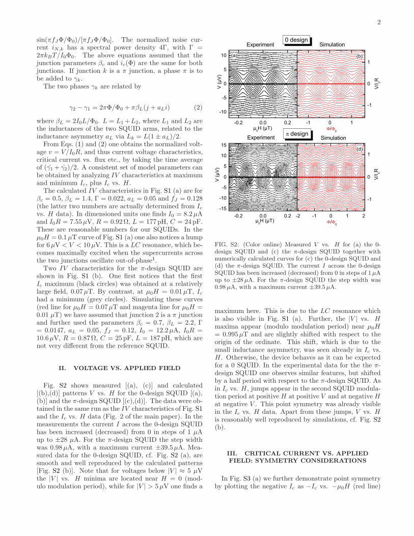
Fig. S2 shows measured [(a), (c)] and calculated[(b),(d)] patterns V vs. H for the 0-design SQUID [(a),(b)] and the π-design SQUID [(c),(d)]. The data were ob-tained in the same run as the IV characteristics of Fig. S1and the Ic vs. H data (Fig. 2 of the main paper). In themeasurements the current I across the 0-design SQUIDhas been increased (decreased) from 0 in steps of 1 µAup to ±28 µA. For the π-design SQUID the step widthwas 0.98µA, with a maximum current ±39.5µA. Mea-sured data for the 0-design SQUID, cf. Fig. S2 (a), aresmooth and well reproduced by the calculated patterns[Fig. S2 (b)]. Note that for voltages below |V | ≈ 5 µVthe |V | vs. H minima are located near H = 0 (mod-ulo modulation period), while for |V | > 5µV one finds a
-10
-5
0
5
10
-0.2 0.0 0.2 -1 0 1
-1
0
1
-0.2 0.0 0.2-15
-10
-5
0
5
10
15
-2 -1 0 1 2
-1
0
1
µ0H (µT)
V (µ
V)
/ 0
(d)(c)
V/I 0R
Experiment
(b)
V (µ
V)
µ0H (µT)
(a)
Simulation design
V/I 0R
/ 0
0 designExperiment Simulation
FIG. S2: (Color online) Measured V vs. H for (a) the 0-design SQUID and (c) the π-design SQUID together withnumerically calculated curves for (c) the 0-design SQUID and(d) the π-design SQUID. The current I across the 0-designSQUID has been increased (decreased) from 0 in steps of 1µAup to ±28µA. For the π-design SQUID the step width was0.98µA, with a maximum current ±39.5µA.
maximum here. This is due to the LC resonance whichis also visible in Fig. S1 (a). Further, the |V | vs. Hmaxima appear (modulo modulation period) near µ0H= 0.995µT and are slightly shifted with respect to theorigin of the ordinate. This shift, which is due to thesmall inductance asymmetry, was seen already in Ic vs.H . Otherwise, the device behaves as it can be expectedfor a 0 SQUID. In the experimental data for the the π-design SQUID one observes similar features, but shiftedby a half period with respect to the π-design SQUID. Asin Ic vs. H , jumps appear in the second SQUID modula-tion period at positive H at positive V and at negativeHat negative V . This point symmetry was already visiblein the Ic vs. H data. Apart from these jumps, V vs. His reasonably well reproduced by simulations, cf. Fig. S2(b).
III. CRITICAL CURRENT VS. APPLIED
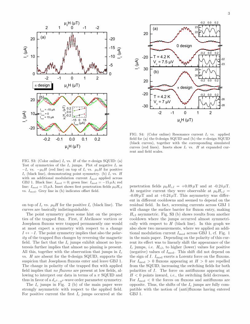
FIELD: SYMMETRY CONSIDERATIONS
In Fig. S3 (a) we further demonstrate point symmetryby plotting the negative Ic as −Ic vs. −µ0H (red line)
3
-2 -1 0 1 20
10
20
-0.2 -0.1 0.0 0.1 0.2
-20
10
20
I c (µA
)
µ0H (µT)
(a)
2 1 0 -1 -2
0
-5
-10
-15
-20
design
I c (µA
)
µ0H (µT)
µ0H (µT)
I c (µA
)
Imod
= 0Imod
= 15 µA
(b)
Imod
= -15 µA
-15 0 15-0.20.00.2
µ 0HcJ
(µT)
Imod (µA)
FIG. S3: (Color online) Ic vs. H of the π-design SQUID: (a)Test of symmetries of the Ic jumps. Plot of negative Ic as−Ic vs. −µ0H (red line) on top of Ic vs. µ0H for positiveIc (black line), demonstrating point symmetry. (b) Ic vs. H
with an additional modulation current Imod applied acrossGBJ 1. Black line: Imod = 0; green line: Imod = −15µA; redline: Imod = 15µA. Inset shows first penetration fields µ0HcJ
vs. Imod. Grey line in (b) indicates offset field.
on top of Ic vs. µ0H for the positive Ic (black line). Thecurves are basically indistinguishable.The point symmetry gives some hint on the proper-
ties of the trapped flux. First, if Abrikosov vortices orJosephson fluxons were trapped permanently one wouldat most expect a symmetry with respect to a changeI ↔ −I. The point symmetry implies that also the polar-ity of the trapped flux changes by reversing the magneticfield. The fact that the Ic jumps exhibit almost no hys-teresis further implies that almost no pinning is present.All this, together with the observation that jumps in Icvs. H are absent for the 0-design SQUID, supports thesuspicion that Josephson fluxons enter and leave GBJ 1.The change in polarity of the trapped flux with appliedfield implies that no fluxons are present at low fields, al-lowing to interpret our data in terms of a π SQUID andthus in favor of a dx2
−y2-wave order parameter symmetry.The Ic jumps in Fig. 2 (b) of the main paper were
strongly asymmetric with respect to the applied field.For positive current the first Ic jumps occurred at the
-2 -1 0 1 2-30
-20
20
30
design
-20
20
I r (µA
)
µ0H (µT)
(b)
T = 4.2 KVc = 7.5 µV
T = 4.2 KVc = 7 µV
(a)
0 design
22
23
-0.2 0.0 0.2
-0.2 0.0 0.2
-23
-22
-0.2 0.0 0.2
26
28
-0.2 0.0 0.2
-28
-26
FIG. S4: (Color online) Resonance current Ir vs. appliedfield for (a) the 0-design SQUID and (b) the π-design SQUID(black curves), together with the corresponding simulatedcurves (red lines). Insets show Ir vs. H at expanded cur-rent and field scales.
penetration fields µ0HcJ = +0.09µT and at -0.24µT.At negative current they were observable at µ0HcJ =-0.09µT and at +0.24µT. This asymmetry was differ-ent in different cooldowns and seemed to depend on theresidual field. In fact, screening currents across GBJ 1will change the surface barrier for fluxon entry, makingHcJ asymmetric. Fig. S3 (b) shows results from anothercooldown where the jumps occurred almost symmetri-cally with respect to H (black line). In this graph wealso show two measurements, where we applied an addi-tional modulation current Imod across GBJ 1, cf. Fig. 1in the main paper. Depending on the polarity of this cur-rent its effect was to linearly shift the appearance of theIc jumps, i.e. HcJ, to higher (lower) values for positive(negative) values of Imod. This shift did not depend onthe sign of I. Imod exerts a Lorentz force on the fluxons.For Imod > 0 fluxons appearing at H > 0 are repelledfrom the SQUID, increasing the switching fields for bothpolarities of I. The force on antifluxons appearing atH < 0 points inward, i.e., the switching field decreases.For Imod < 0 the forces on fluxons and antifluxons areopposite. Thus, the shifts of the Ic jumps are fully com-patible with the notion of (anti)fluxons having enteredGBJ 1.
4
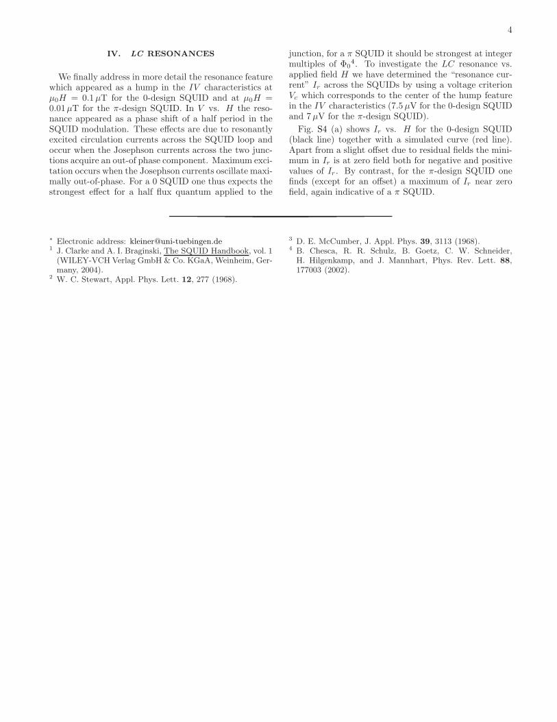
IV. LC RESONANCES
We finally address in more detail the resonance featurewhich appeared as a hump in the IV characteristics atµ0H = 0.1µT for the 0-design SQUID and at µ0H =0.01µT for the π-design SQUID. In V vs. H the reso-nance appeared as a phase shift of a half period in theSQUID modulation. These effects are due to resonantlyexcited circulation currents across the SQUID loop andoccur when the Josephson currents across the two junc-tions acquire an out-of phase component. Maximum exci-tation occurs when the Josephson currents oscillate maxi-mally out-of-phase. For a 0 SQUID one thus expects thestrongest effect for a half flux quantum applied to the
junction, for a π SQUID it should be strongest at integermultiples of Φ0
4. To investigate the LC resonance vs.applied field H we have determined the “resonance cur-rent” Ir across the SQUIDs by using a voltage criterionVc which corresponds to the center of the hump featurein the IV characteristics (7.5µV for the 0-design SQUIDand 7µV for the π-design SQUID).
Fig. S4 (a) shows Ir vs. H for the 0-design SQUID(black line) together with a simulated curve (red line).Apart from a slight offset due to residual fields the mini-mum in Ir is at zero field both for negative and positivevalues of Ir . By contrast, for the π-design SQUID onefinds (except for an offset) a maximum of Ir near zerofield, again indicative of a π SQUID.
∗ Electronic address: [email protected] J. Clarke and A. I. Braginski, The SQUID Handbook, vol. 1(WILEY-VCH Verlag GmbH & Co. KGaA, Weinheim, Ger-many, 2004).
2 W. C. Stewart, Appl. Phys. Lett. 12, 277 (1968).
3 D. E. McCumber, J. Appl. Phys. 39, 3113 (1968).4 B. Chesca, R. R. Schulz, B. Goetz, C. W. Schneider,H. Hilgenkamp, and J. Mannhart, Phys. Rev. Lett. 88,177003 (2002).


![1) 2) 3) 4) arXiv:2004.14222v1 [cond-mat.mes-hall] …for atomic reconstruction Johannes Holler, 1Sebastian Meier, Michael Kempf,1,2 Philipp Nagler,1 Kenji Watanabe,3 Takashi Taniguchi,4](https://img.pdfslide.net/doc/110x75/5f1c03303306e92e0d496f93/1-2-3-4-arxiv200414222v1-cond-matmes-hall-for-atomic-reconstruction-johannes.jpg)