Embed Size (px)
DESCRIPTION
TV PHILIPS AO2E SEVICE MANUAL
Citation preview
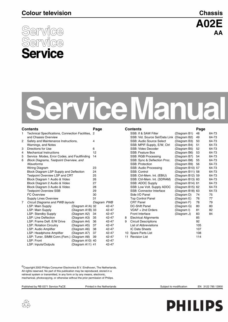
Colour television Chassis
Published by RB 0371 Service PaCE
©Copyright 2003 Philips Consumer EAll rights reserved. No part of this puretrieval system or transmitted, in anymechanical, photocopying, or otherw
A02EAA
Contents Page Contents Page1 Technical Specifications, Connection Facilities, 2
and Chassis Overview2 Safety and Maintenance Instructions, 4
Warnings, and Notes3 Directions for Use 64 Mechanical Instructions 125 Service Modes, Error Codes, and Faultfinding 146 Block Diagrams, Testpoint Overview, and
WaveformsWiring Diagram 23Block Diagram LSP Supply and Deflection 24Testpoint Overview LSP and CRT 25Block Diagram 1 Audio & Video 26Block Diagram 2 Audio & Video 27Block Diagram 3 Audio & Video 28Testpoint Overview SSB 29I2C Overview 30Supply Lines Overview 31
7 Circuit Diagrams and PWB layouts Diagram PWBLSP: Main Supply (Diagram A1A) 32 42-47LSP: Main Supply (Diagram A1B) 33 42-47LSP: Standby Supply (Diagram A2) 34 42-47LSP: Line Deflection (Diagram A3) 35 42-47LSP: Frame Defl. E/W Drive (Diagram A4) 36 42-47LSP: Rotation Circuitry (Diagram A5) 37 42-47LSP: Audio Amplifier (Diagram A6) 38 42-47LSP: Headphone Amplifier (Diagram A7) 37 42-47LSP: Tuner, SIMM Conn.(Fem.) (Diagram A8) 39 42-47LSP: Front (Diagram A10) 40 42-47LSP: Inputs/Outputs (Diagram A11) 41 42-47
SSB: If & SAW Filter (Diagram B1) 48 64-73SSB: Vid. Source Sel/Data Link (Diagram B2) 49 64-73SSB: Audio Source Select (Diagram B3) 50 64-73SSB: MPIF-Supply, E/W, Ctrl (Diagram B4) 51 64-73SSB: Video Decoder (Diagram B5) 52 64-73SSB: Feature Box (Diagram B6) 53 64-73SSB: RGB Processing (Diagram B7) 54 64-73SSB: Sync & Deflection Proc. (Diagram B8) 55 64-73SSB: Protection (Diagram B9) 56 64-73SSB: Audio Processing (Diagram B10) 57 64-73SSB: Control (Diagram B11) 58 64-73SSB: Ctrl-Mem. Int. (EBIU) (Diagram B12) 59 64-73SSB: Ctrl-Mem. Int. (SDRAM) (Diagram B13) 60 64-73SSB: ADOC Supply (Diagram B14) 61 64-73SSB: Low Volt. Supply ADOC (Diagram B15) 62 64-73SSB: Connector Interface (Diagram B18) 63 64-73Side I/O Panel (Diagram D) 74 75Top Control Panel (Diagram E) 76 77CRT Panel (Diagram F) 78 79DC-Shift Panel (Diagram G) 80 80VDAF + 2nd Orders (Diagram I) 81 82Front Interface (Diagram J) 83 84
8 Electrical Alignments 859 Circuit Descriptions 92
List of Abbreviations 105IC Data Sheets 107
10 Spare Parts List 10811 Revision List 114
Printed in the Netherlands Subject to modification EN 3122 785 13950
lectronics B.V. Eindhoven, The Netherlands.blication may be reproduced, stored in a form or by any means, electronic,
ise without the prior permission of Philips.
Technical Specifications, Connections, and Chassis OverviewEN 2 A02E1.
1. Technical Specifications, Connections, and Chassis Overview
Index of this chapter:1. Technical Specifications2. Connections3. Chassis Overview Note: Figures below can deviate slightly from the actual situation, due to the different set executions.
1.1 Technical Specifications
1.1.1 Vision
Display type : CRT, Real FlatScreen size(s) : 28 inch - 16:9
: 29 inch - 4:3: 32 inch - 16:9
Tuning system : PLLIF frequency : 38.9 MHzColour systems : PAL: B/G,D/K,I
: SECAM: B/G,D/K,L/L’: NTSC-playback
Channel selections : 100 presets: UVSH
Aerial input : 75 ohm, IEC-type
1.1.2 Sound
Sound systems : FM-mono, AM-mono: FM-stereo: B/G: NICAM: B/G,D/K,I,L
Maximum power : 4 x 10 W_rms (int.)
1.1.3 Miscellaneous
Mains voltage : 220 - 240 VacMains frequency : 50 / 60 HzAmbient temperature : +5 to +45 deg. CMaximum humidity : 90 % R.H.Power consumption :- Normal operation : ≈ 115 W- Standby : < 1 W
1.2 Connections
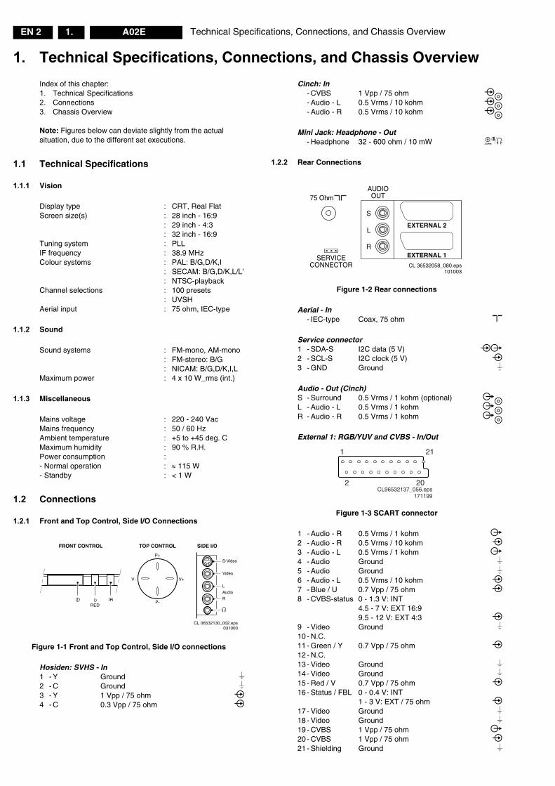
1.2.1 Front and Top Control, Side I/O Connections
Figure 1-1 Front and Top Control, Side I/O connections
Hosiden: SVHS - In1 - Y Ground
2 - C Ground
3 - Y 1 Vpp / 75 ohm 4 - C 0.3 Vpp / 75 ohm
Cinch: In- CVBS 1 Vpp / 75 ohm - Audio - L 0.5 Vrms / 10 kohm
- Audio - R 0.5 Vrms / 10 kohm
Mini Jack: Headphone - Out- Headphone 32 - 600 ohm / 10 mW
1.2.2 Rear Connections
Figure 1-2 Rear connections
Aerial - In- IEC-type Coax, 75 ohm
Service connector1 - SDA-S I2C data (5 V)
2 - SCL-S I2C clock (5 V)
3 - GND Ground
Audio - Out (Cinch)S - Surround 0.5 Vrms / 1 kohm (optional)
L - Audio - L 0.5 Vrms / 1 kohm
R - Audio - R 0.5 Vrms / 1 kohm
External 1: RGB/YUV and CVBS - In/Out
Figure 1-3 SCART connector
1 - Audio - R 0.5 Vrms / 1 kohm
2 - Audio - R 0.5 Vrms / 10 kohm
3 - Audio - L 0.5 Vrms / 1 kohm 4 - Audio Ground
5 - Audio Ground
6 - Audio - L 0.5 Vrms / 10 kohm 7 - Blue / U 0.7 Vpp / 75 ohm
8 - CVBS-status 0 - 1.3 V: INT4.5 - 7 V: EXT 16:99.5 - 12 V: EXT 4:3
9 - Video Ground
10 - N.C. 11 - Green / Y 0.7 Vpp / 75 ohm
12 - N.C. 13 - Video Ground 14 - Video Ground
15 - Red / V 0.7 Vpp / 75 ohm
16 - Status / FBL 0 - 0.4 V: INT1 - 3 V: EXT / 75 ohm
17 - Video Ground
18 - Video Ground 19 - CVBS 1 Vpp / 75 ohm
20 - CVBS 1 Vpp / 75 ohm
21 - Shielding Ground
CL 06532130_002.eps031000
S-Video
Video
L
Audio
R
SIDE I/OFRONT CONTROL
V+V-
P-
P+
IRRED
TOP CONTROL
L
S
R
AUDIOOUT75 Ohm
SERVICECONNECTOR CL 36532058_080.eps
101003
EXTERNAL 2
EXTERNAL 1
1 21
202CL96532137_056.eps
171199
Technical Specifications, Connections, and Chassis Overview EN 3A02E 1.
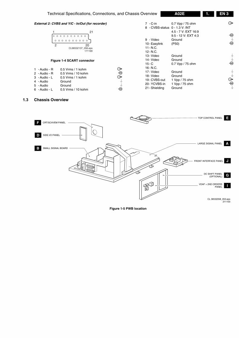
External 2: CVBS and Y/C - In/Out (for recorder)
Figure 1-4 SCART connector
1 - Audio - R 0.5 Vrms / 1 kohm
2 - Audio - R 0.5 Vrms / 10 kohm
3 - Audio - L 0.5 Vrms / 1 kohm 4 - Audio Ground
5 - Audio Ground
6 - Audio - L 0.5 Vrms / 10 kohm
7 - C-in 0.7 Vpp / 75 ohm
8 - CVBS-status 0 - 1.3 V: INT4.5 - 7 V: EXT 16:99.5 - 12 V: EXT 4:3
9 - Video Ground
10 - Easylink (P50) 11 - N.C. 12 - N.C. 13 - Video Ground 14 - Video Ground
15 - C 0.7 Vpp / 75 ohm
16 - N.C. 17 - Video Ground
18 - Video Ground
19 - CVBS-out 1 Vpp / 75 ohm 20 - YCVBS-in 1 Vpp / 75 ohm
21 - Shielding Ground
1.3 Chassis Overview
Figure 1-5 PWB location
1 21
202CL96532137_056.eps
171199
CL 36532058_053.eps211103
LARGE SIGNAL PANEL A
VDAF + 2ND ORDERSPANEL I
DC SHIFT PANEL(OPTIONAL) G
SMALL SIGNAL BOARDB
CRT/SCAVEM PANELF
FRONT INTERFACE PANEL J
TOP CONTROL PANEL E
SIDE I/O PANELD
Service Modes, Error Codes, and Fault FindingEN 14 A02E5.
5. Service Modes, Error Codes, and Fault Finding
Index of this chapter:1. Test points2. Service Modes3. Problems and solving tips (related to CSM)4. ComPair5. Error Codes6. The blinking LED procedure7. Protections8. Repair tips9. Software downloading
5.1 Test Points
See chapter 6 " Block Diagrams, Testpoint Overview, and Waveforms". Perform measurements under the following conditions:• Service Default Mode.• Video: colour bar signal.• Audio: 3 kHz left, 1 kHz right.
5.2 Service Modes
Service Default Mode (SDM) and Service Alignment Mode (SAM) offer several features for the service technician, while the Customer Service Mode (CSM) is used for communication between a Philips Customer Care Centre (P3C) and a customer. There is also the option of using ComPair, a hardware interface between a computer (see requirements below) and the TV chassis. It offers the ability of structured troubleshooting, test pattern generation, error code reading, software version readout, and software upgrading. Minimum requirements: a Pentium processor, Windows 95/98, and a CD-ROM drive (see also paragraph “ComPair”).
5.2.1 Service Default Mode (SDM)
Purpose• To create a pre-defined setting, to get the same
measurement results as given in this manual.• To override SW protections (only when SDM is activated
via shorting the SDM pins on the SSB).• To start the blinking LED procedure.• Inspection of error buffer, life timer, and software version.
Specifications• Tuning frequency: 475.25 MHz for PAL/SECAM.• Colour system: SECAM L for France or PAL B/G for the
rest of Europe.• All picture settings at 50 % (brightness, colour, contrast).• All sound settings at 50 %, except volume at 25 %. • All service-unfriendly modes (if present) are disabled, like:
– (Sleep) timer.– Child/parental lock.– Blue mute.– Automatic volume limiter (AVL).– Auto switch-off (when no video signal was received for
10 minutes).– Skip/blank of non-favourite pre-sets.– Hotel or hospital mode.– Local keyboard block.– Smart modes.– Auto store of personal presets.– Auto user menu time-out.
How to Activate SDMUse one of the following methods:
• Use the standard RC-transmitter and key in the code “062596”, directly followed by the “MENU” button. Note: It is possible that, together with the SDM, the main menu will appear. To switch it "off", push the “MENU” button again.
• Short circuit, during switch "on" of the set, the two solder pads on the SSB with the indication “FOR SERVICE”. These solder pads are located at the "tuner" side of the SSB (just above the large BGA IC). Caution: If the SDM is activated via these pins, all the software-controlled protections are de-activated for 15 s. When these 15 s are expired, the set will shutdown to protection mode.
• Use the DST-emulation feature of ComPair.• Use the “DEFAULT” button on the Dealer Service Tool
(RC7150). After activating this mode:• “SDM” will appear in the upper right corner of the screen.• Also, the error buffer, operating hours, and software
version are displayed (can be toggled "on/off" with the "STATUS / OSD / [i+]" button).
• Blinking LED procedure will be started.• All software-controlled protections are overridden for 15 s.
When these 15 s are expired, the set will shutdown to protection mode.
Contents of SDM:• HRS. Displays the accumulated total of operation hours
(not the standby hours) in hexadecimal value.• SW. Displays the date of the software and the software
version of the ROM example: A02EB1_1.00 = AAABBC-X.YY. – AAA= chassis name.– BB= region and/or function name: E= Europe, A= Asia
Pacific, U= NAFTA, L= LATAM, B= Basic, T= Top, P= PAL, N= NTSC, S= Stereo, M= Mono.
– C= the language cluster number.– X.Y= the software version, where X is the main version
number (different numbers are not compatible with one another) and Y is the sub version number (a higher number is always compatible with a lower number).
• ERR (followed by maximal 8 errors). The most recent error is displayed at the upper left (for an error explanation see paragraph “Error Codes”).
How to navigate• When you press the “MENU” button on the RC transmitter,
the set will toggle between the SDM and the normal user menu (with the SDM mode still active in the background).
• When you press the “STATUS / OSD / [i+]” button on the RC transmitter, the set will toggle only display "SDM". This mode is useful when performing measurements, then the OSD info will not generate interference.
How to exit SDMUse one of the following methods:• Switch the set to STANDBY via a standard customer RC-
transmitter (the error buffer is erased).• Via a standard customer RC-transmitter: key in “00”-
sequence (the error buffer is not erased).
5.2.2 Service Alignment Mode (SAM)
Purpose• To perform alignments.• To change option settings.• To easily identify the used software version.• To view operation hours.• To display / clear the error code buffer.
Service Modes, Error Codes, and Fault Finding EN 15A02E 5.
Specifications• Operating hours counter.• Software version.• Option settings.• Error buffer reading and erasing.• Software alignments.• Disable service unfriendly modes.
How to activate SAMUse one of the following methods:• Via a standard RC transmitter: key in the code “062596”
directly followed by the “STATUS / OSD / [i+]” button.• Use the DST-emulation feature of ComPair.• Press the "ALIGN" button on the DST while the set is in the
normal operation After activating this mode, “SAM” will appear in the upper right corner of the screen.
Contents of SAM:• HRS. Displays the accumulated total of operation hours
(not the standby hours) in hexadecimal value Note: every time the set is switched "on" by the mains switch or the RC, the timer is increased by 0.5.
• SW. Displays the software version of the ROM example: A02EB1_1.00 = AAABBC-X.YY. – AAA= chassis name.– BB= region and/or function name: E= Europe, A= Asia
Pacific, U= NAFTA, L= LATAM, B= Basic, T= Top, P= PAL, N= NTSC, S= Stereo, M= Mono.
– C= the language cluster number.– X.Y= the software version, where X is the main version
number (different numbers are not compatible with one another) and Y is the sub version number (a higher number is always compatible with a lower number).
• ERR (followed by maximal 8 errors). The most recent error is displayed at the upper left (for an error explanation see paragraph “Error Codes”).
• CLEAR ERRORS. When you press the “OK” button, the error buffer is reset.
• OPTIONS. Extra features for Service.• AKB. Disable (off) or enable (on) the "black current loop"
(AKB= Auto Kine Bias). For Vg2 alignment.• VSD. Disable (off) or enable (on) the vertical deflection
(VSD= Vertical Scan Disable).Do not use (will cause a protection). Is for future use.
• TUNER. This will activate the “TUNER” alignments sub-menu.
• WHITE TONE. This will activate the “WHITE TONE” alignments sub-menu.
• GEOMETRY. This will activate the “GEOMETRY” alignments sub-menu.
• SOUND. This will activate the “SOUND” alignments sub-menu.
• SMART SETTINGS. This will activate the “SMART SETTINGS” alignments sub-menu.
• STORE. This will save the new settings/alignments.• EEPROM TEST. This will report if the SW checksum is OK.
Convenient after SW upgrading.• VID RAM TEST. This will check the continuity of the
address bus and data bus of the Video RAM.• VG2. This feature is not implemented yet. Do not use. Note: Alignments are described in chapter 8 "Alignments".
How to navigate• In SAM, you can select the menu items with the “CURSOR
UP/DOWN” key on the RC-transmitter. The selected item will be highlighted. When not all menu items fit on the screen, move the “CURSOR UP/DOWN” key to display the next/previous menu items.
• With the “CURSOR LEFT/RIGHT” keys, it is possible to:– (De) activate the selected menu item.– Change the value of the selected menu item.
– Activate the selected submenu.• When you press the “MENU” button on the RC transmitter,
the set will toggle between the SAM and the normal user menu (with the SAM mode still active in the background).
How to exit SAMUse one of the following methods:• Switch the set to STANDBY via the RC-transmitter (the
error buffer is erased).• Via a standard customer RC-transmitter: key in “00”-
sequence (the error buffer is not erased).
5.2.3 Customer Service Mode (CSM)
PurposeWhen a customer is having problems with his TV-set, he can call his dealer or the Philips helpdesk (P3C). The service technician can than ask the customer to activate the CSM, in order to identify the status of the set. Now, the service technician can judge the severity of the complaint. In many cases, he can advise the customer how to solve the problem, or he can decide if it is necessary to visit the customer.The CSM is a read only mode; therefore, modifications in this mode are not possible.
How to activate CSMUse one of the following methods:• Press the “MUTE” button on the RC-transmitter
simultaneously with any key on the TV for at least 4 seconds.
• Key in the code “123654” via the standard RC transmitter. Notes: • Activation of the CSM is only possible if there is no (user)
menu on the screen!• During CSM, sound volume is set to 25% of the scale,
"Smart Sound" is set to "Theatre" mode, and "Smart Picture" is set to "Rich/Movies" mode temporarily to ensure a good picture and sound of the working set. After leaving CSM, the original settings are restored.
How to navigateBy means of the “CURSOR-DOWN/UP” knob on the RC-transmitter, you can navigate through the menus.
Contents of CSMThe following information is displayed on screen:• Text “CSM” on the first line.• Line number for every line (to make CSM language
independent).• Option code information.• Configuration information.• Service-unfriendly modes. 1. 28PW8609/12 (if present). Type/model number according
to the Philips standard.2. SOFTWARE. Software version AAABBC-X.YY.3. HOURS ON. Operating hours (in hexadecimal).4. CODES. Shows the contents of the error buffer (the word
“error” may not be used on this screen, instead “codes” is used).
5. OP. Option code information.6. SYSTEM. "XXXXXX" is the (colour) system that is set for
this preset (this is not applicable to NAFTA and AP-NTSC models).
7. NO SIGNAL. No "ident" signal present (VID status bit in MPIF) on selected source.
8. TIMER ON (if present). Timer (in "FEATURE" menu) is activated.
9. CHANNEL LOCKED (if present). Child Lock is activated (i.e. when local keyboard is locked).
10. NOT PREFERED (if present). Current channel is defined as skipped or non-preferred.
Service Modes, Error Codes, and Fault FindingEN 16 A02E5.
11. HOTELMODE ON/OFF (if present). Shows if the HOTEL mode is activated (only for Europe and AP).
12. SOURCE. Selected source before entry of CSM; XXX (channel no.), external source name (i.e. AV1, CVI, EXT1, etc...).
13. SOUND. Selected SOUND mode; "XX"= MONO, NICAM, STEREO, L1 (Language 1), L2 (Language 2), SAP, VIRTUAL, or DIGITAL prior entry to CSM.
14. VOLUME. Volume level before entry of CSM (typ. 00..100).15. BALANCE. Balance level before entry of CSM (typ. -
50..50).16. BRIGHTNESS. Brightness level before entry of CSM (typ.
00..100).17. COLOR. Colour level before entry of CSM (typ. 00..100).18. CONTRAST. Contrast level before entry of CSM (typ.
00..100).19. HUE (if present). Hue level before entry of CSM (typ. -
50..100).
How to exit CSMUse one of the following methods:• After you press a key on the RC-transmitter (with exception
of the “CHANNEL”, “VOLUME” and digit (0-9) keys), or • After you switch the TV-set “OFF” with the mains switch.• After 15 min. no RC or local keyboard actions.
5.3 Problems and Solving Tips (related to CSM)
Note: Below described problems are all related to the TV settings. The procedures to change the value (or status) of the different settings are described above. New value(s) are automatically stored.
5.3.1 Picture Problems
Picture too dark1. Press SMART PICTURE on the RC. In case the picture
improves, increase the “Brightness” or the “Contrast” value. The new value(s) are automatically stored (in “personal” pre-set) for all TV channels.
2. Check in CSM lines BRIGHTNESS and/or CONTRAST. If the value of line BRIGHTNESS is low (< 10) or the value of line CONTRAST is low (< 10), increase them.
Picture too bright1. Press SMART PICTURE on the RC. In case the picture
improves, decrease the “Brightness” or the “Contrast” value. The new value(s) are automatically stored (in “personal” pre-set) for all TV channels.
2. Check in CSM lines BRIGHTNESS and/or CONTRAST. If the value of line BRIGHTNESS is high (> 40) or the value of line CONTRAST is high (> 50), decrease the “Brightness” or the “Contrast” value.
White line around picture elements and text1. Press SMART PICTURE on the RC. In case the picture
improves, decrease the “Sharpness” value. The new value is automatically stored (in “personal” pre-set) for all TV channels.
2. Check in CSM line SHARPNESS. Decrease the “Sharpness” value. The new value is automatically stored for all TV channels.
No pictureCheck in CSM line 7. In case this line shows NO SIGNAL, check the aerial cable/aerial system.
Blue pictureNo proper signal is received. Check the aerial cable/aerial system.
Blue picture and/or unstable pictureA scrambled or decoded signal is received.
Black and white pictureCheck in CSM line COLOR. In case the value is low (< 10), increase the “Color” value. The new value is automatically stored for all TV channels.
No colours/colour lines around picture elements or colours not correct or unstable picture1. Check in CSM line SYSTEM. If a “strange” system pops up,
something has gone wrong during installation. Re-install the channel.
2. In case line SYSTEM is “FRANCE”, the installed system for this pre-set is SECAM, while PAL is required. Install the required program again: open the installation menu and perform manual installation. Select system “West Europe”.
Menu text not sharp enough1. Press “SMART PICTURE”. In case picture improves,
decrease the "Contrast" value. The new value(s) are automatically stored for all TV channels.
2. Check in CSM line CONTRAST. If the value of this line is high (> 50), decrease the "Contrast" value.
5.3.2 Sound Problems
No sound from left and right speakerCheck in CSM line VOLUME. If the value is high, increase the value of “Volume”. The new value(s) are automatically stored (in “personal” pre-set) for all TV channels.
Sound too loud for left and right speakerCheck in CSM line VOLUME. If the value is low, decrease the value of “Volume”. The new value(s) are automatically stored (in “personal” pre-set) for all TV channels.
5.4 ComPair
5.4.1 Introduction
ComPair (Computer Aided Repair) is a service tool for Philips Consumer Electronics products. ComPair is a further development on the European DST (service remote control), which allows faster and more accurate diagnostics. ComPair has three big advantages:• ComPair helps you to quickly get an understanding on how
to repair the chassis in a short time by guiding you systematically through the repair procedures.
• ComPair allows very detailed diagnostics (on I2C level) and is therefore capable of accurately indicating problem areas. You do not have to know anything about I2C commands yourself because ComPair takes care of this.
• ComPair speeds up the repair time since it can automatically communicate with the chassis (when the microprocessor is working) and all repair information is directly available. When ComPair is installed together with the SearchMan electronic manual of the defective chassis, schematics and PWBs are only a mouse click away.
5.4.2 Specifications
ComPair consists of a Windows based faultfinding program and an interface box between PC and the (defective) product. The ComPair interface box is connected to the PC via a serial or RS232 cable. For this chassis, the ComPair interface box and the TV communicate via a bi-directional service cable via the service connector.
Service Modes, Error Codes, and Fault Finding EN 17A02E 5.
The ComPair faultfinding program is able to determine the problem of the defective television. ComPair can gather diagnostic information in two ways:• Automatic (by communication with the television):
ComPair can automatically read out the contents of the entire error buffer. Diagnosis is done on I2C level. ComPair can access the I2C bus of the television. ComPair can send and receive I2C commands to the micro controller of the television. In this way, it is possible for ComPair to communicate (read and write) to devices on the I2C busses of the TV-set.
• Manually (by asking questions to you): Automatic diagnosis is only possible if the micro controller of the television is working correctly and only to a certain extends. When this is not the case, ComPair will guide you through the faultfinding tree by asking you questions (e.g. Does the screen give a picture? Click on the correct answer: YES / NO) and showing you examples (e.g. Measure test-point I7 and click on the correct oscillogram you see on the oscilloscope). You can answer by clicking on a link (e.g. text or a waveform picture) that will bring you to the next step in the faultfinding process.
By a combination of automatic diagnostics and an interactive question / answer procedure, ComPair will enable you to find most problems in a fast and effective way. Beside fault finding, ComPair provides some additional features like:• Up- or downloading of pre-sets.• Managing of pre-set lists.• Emulation of the Dealer Service Tool (DST).• If both ComPair and SearchMan (Electronic Service
Manual) are installed, all the schematics and the PWBs of the set are available by clicking on the appropriate hyperlink.Example: Measure the DC-voltage on capacitor C2568 (Schematic/Panel) at the Mono-carrier.– Click on the “Panel” hyperlink to automatically show
the PWB with a highlighted capacitor C2568. – Click on the “Schematic” hyperlink to automatically
show the position of the highlighted capacitor.• SW upgrading
5.4.3 Stepwise Start-up
This is realised via ComPair and is very helpful when a protection is activated (see also chapter “Protections”). Under normal circumstances, a fault in the power supply, or an error during start-up, will switch the television to protection mode. ComPair can take over the initialisation of the television. In this way, it is possible to distinguish which part of the start-up routine (hence which circuitry) is causing the problem. Take notice that the transition between two steps can take some time, so give the set some time to reach a stable state. During the transition time, the LED can blink strangely. On activating Service mode, protections and other errors can be trapped by powering the TV in stepwise fashion as explained below. The "stepwise start-up" mode is done in the specified sequence. Before activating this mode, all the protections are disabled and are only enabled step-by-step, to trap the errors more appropriately. The following steps are involved.Step 0: Standby.• Pre-condition: The set is in protection mode.• Post-condition: The set is switched to the stepwise start-up
mode. Only the necessary Standby Supply is present, all other supplies are switched "off".
Step 1: Power "on". • Pre-condition: All protections are disabled, sound
amplifiers are muted, and general initialisation is done.
• Post-condition: 8V and 5V supplies are "on". Degaussing is "on" and switched "off" after 3 s. The supply fault protections are enabled.
Step 2: Initialised.• Pre-condition: Step 1 is done. No supply protection faults
are detected.• Post-condition: ADOC, MPIF, and Tuner components are
initialised. Step 3: Deflection "on".• Pre-condition: Step 2 is done. No protection faults
detected.• Post-condition: Deflection is switched "on". The horizontal
deflection fault protections are enabled.Step 4: TV "on".• Pre-condition: Step 3 is done. No protection faults
detected.• Post-condition: Picture tube is switched "on". Sound
amplifiers are demuted. The X-ray/beam current fault protections are enabled.
Note: When the set is in stepwise mode and, due to stepping-up, a protection is activated, the set will really go into protection (blinking LED). The set will not leave the stepwise-mode however. If state X is the state where the set went to protection, stepwise start-up will return to state X-1. At state (X-1) diagnostic measurements can be performed. Also, in the short time, the set is in state X but not in protection, you can also do some measurements.
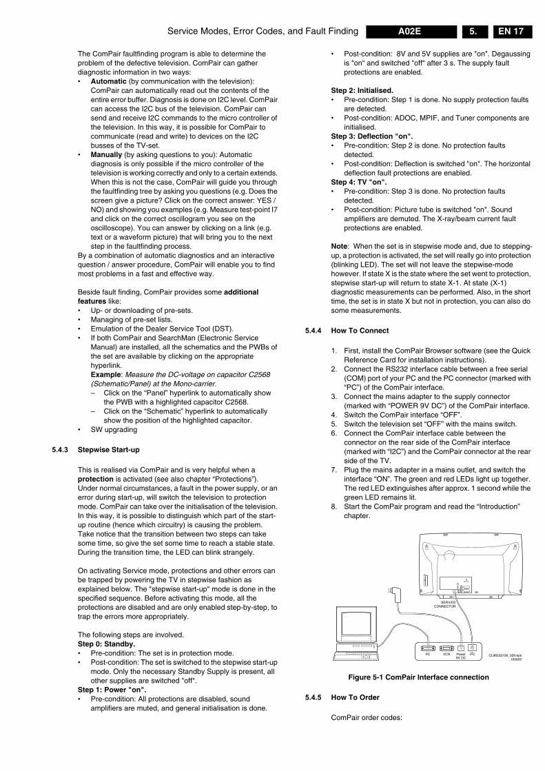
5.4.4 How To Connect
1. First, install the ComPair Browser software (see the Quick Reference Card for installation instructions).
2. Connect the RS232 interface cable between a free serial (COM) port of your PC and the PC connector (marked with “PC”) of the ComPair interface.
3. Connect the mains adapter to the supply connector (marked with “POWER 9V DC”) of the ComPair interface.
4. Switch the ComPair interface “OFF”.5. Switch the television set “OFF” with the mains switch.6. Connect the ComPair interface cable between the
connector on the rear side of the ComPair interface (marked with “I2C”) and the ComPair connector at the rear side of the TV.
7. Plug the mains adapter in a mains outlet, and switch the interface “ON”. The green and red LEDs light up together. The red LED extinguishes after approx. 1 second while the green LED remains lit.
8. Start the ComPair program and read the “Introduction” chapter.
Figure 5-1 ComPair Interface connection
5.4.5 How To Order
ComPair order codes:
CL96532156_029.eps190600
PC VCR I2CPower9V DC
R
L
AUDIO EXTERNAL 1
EXTERNAL 2
SERVICECONNECTOR
Service Modes, Error Codes, and Fault FindingEN 18 A02E5.
• Starter kit ComPair32/SearchMan32 software and ComPair interface (excl. transformer): 3122 785 90450.
• ComPair interface (excluding transformer): 4822 727 21631.
• Starter kit ComPair32 software (registration version): 3122 785 60040.
• Starter kit SearchMan32 software: 3122 785 60050.• ComPair32 CD (2003 update): 3122 785 60110.• SearchMan32 CD (2003 update): 3122 785 60120.• ComPair interface cable: 3122 785 90004.• ComPair firmware upgrade IC: 3122 785 90510.• Transformer Europe: 4822 727 21632.• Transformer UK: 4822 727 21633.
5.5 Error Codes
5.5.1 Introduction
The error code buffer contains all detected errors since the last time the buffer was erased. The buffer is written from left to right, new errors are logged at the left side, and all other errors shift one position to the right. When an error has occurred, the error is added to the list of errors, provided the list is not full or the error is a protection error. When an error occurs and the error buffer is full, then the new error is not added, and the error buffer stays intact (history is maintained), except when the error is a protection error. To prevent that an occasional error stays in the list forever, the error is removed from the list after 50+ operation hours. When multiple errors occur (errors occurred within a short time span), there is a high probability that there is some relation between them.
5.5.2 How to read the Error Buffer
Use one of the following methods:• On screen via the SAM (only if you have a picture).
Examples:– 0 0 0 0: No errors detected– 6 0 0 0: Error code 6 is the last and only detected error– 9 6 0 0: Error code 6 was first detected and error code
9 is the last detected error• Via the blinking LED procedure (when you have no
picture). See next paragraph.• Via ComPair.
5.5.3 How to clear the Error Buffer
Use one of the following methods:• By activation of the “CLEAR ERRORS” command in the
SAM menu.• With a normal RC, key in sequence “MUTE” followed by
“062599” and “OK”.• When you transmit the commands “DIAGNOSE” - “99” -
“OK” with ComPair (or with a DST).• If the content of the error buffer has not changed for 50+
hours, it resets automatically.
5.5.4 Error Codes
Error codes are required to indicate failures in the TV set. In principle a unique error is available for every:• I2C device error.• I2C bus error (for every bus containing two or more I2C
devices).• Protection error (e.g. +8V protection or Horizontal
protection).• Error not related to an I2C device, but of importance (e.g.
BC-loop, RAM error).
Table 5-1 Error Table
Service tips:• In case of non-intermittent faults, clear the error buffer
before you begin the repair. This to ensure that old error codes are no longer present. Before clearing the buffer, write down the content, as this history can give you significant information.
• If possible, check the entire contents of the error buffer. In some situations, an error code is only the result of another error code and not the actual cause (e.g., a fault in the protection detection circuitry can also lead to a protection).
5.6 The Blinking LED Procedure
5.6.1 Introduction
Via this procedure, you can make the contents of the error buffer visible via the front LED. This is especially useful for fault finding, when there is no picture. When the SDM is activated, the front LED will show (blink) the contents of the error-buffer. Error-codes > 10 are shown as follows:1. A long blink of 750 ms (which is an indication of the decimal
digit),2. A pause of 1500 ms,3. “n” short blinks (where “n” = 1 - 9),4. When all the error-codes are displayed, the sequence
finishes with a LED blink of 3000 ms,5. The sequence starts again. Example: Error 12 9 6 0 0. After activation of the SDM, the front LED will show: 1. 1 long blink of 750 ms (which is an indication of the decimal
digit) followed by a pause of 1500 ms,2. 2 short blinks of 250 ms, followed by a pause of 3000 ms,3. 9 short blinks of 250 ms, followed by a pause of 3000 ms,4. 6 short blinks of 250 ms, followed by a pause of 3000 ms,5. 1 long blink of 3000 ms to finish the sequence,6. The sequence starts again.
5.6.2 How to activate
Use one of the following methods:• Activate the SDM (only via soldering pads marked “FOR
SERVICE” on the SSB). The blinking front LED will show the entire contents of the error buffer (this works in “normal
Error Description
0 No error
1 Horizontal Protection (via NOHFB bit in ADOC)
3+8V error (missing/protection active by checking MPIF ASUP bit))
4X-ray/High beam current protection signal (via XPROT bit in ADOC)
5 Hardware Protection is active (same as EMG)
7 Under-voltage protection
11 MPIF I2C communication failure / MPIF test failed
12BC-loop not stabilised within the time limit (i.e. after timer is expired)
13 NVM I2C communication failure
14 Main tuner I2C failure UV13xx
17 3D Combfilter I2C communication failure
18 PIP Tuner I2C failure
19 2fH component input I2C failure (PCF8574)
21PIP IF demodulator IC TDA988x communication failed (only for PIP/DW sets)
22Flash over protection error (to register CRT flash-overs, via FPR bit in ADOC)

Service Modes, Error Codes, and Fault Finding EN 19A02E 5.
operation” mode and in “protection” mode). In order to avoid confusion with RC5 signal reception blinking, this LED blinking procedure is terminated when an RC5 command is received.
• Transmit the commands “MUTE”, “06250x”, and “OK” with a normal RC (where “x” is the position in the error buffer that has to be displayed). With x= 1, the last detected error is shown, x= 2 the second last error, etc.... When x= 0, all errors are shown.
• “DIAGNOSE X” with the DST (where “x” is the position in the error buffer that has to be displayed). With x= 1, the last detected error is shown, x= 2 the second last error, etc.... When x= 0, all errors are shown.
Note: It can take some seconds before the blinking LED starts.
5.7 Protections
5.7.1 Introduction
Fault protections are introduced to avoid unacceptable temperature rising and burning hazards. If a fault situation is detected, an error code will be generated and if necessary, the set is put in protection mode. The protection mode is indicated by the blinking of the front LED at a frequency of 3 Hz (or by a coded blinking in special cases). For the customer, it is made impossible to switch "on" the set during a protection.It is possible to determine the type of fault by interpreting the blinking pattern of the LED indicator. It is also possible to read out the error codes from the NVM via ComPair. It is possible to de-activate the protection states in the Service Default Mode. The following protections are implemented:
Table 5-2 Protections overview
The protections are split up in the following order:• I2C related protections.• ADOC related protections (via polling on I/O pins or via
algorithms).• DOP related protections (mainly for deflection items).• Hardware errors that are not sensed by the OTC (e.g.
vertical flyback protection, bridge coil protection, E/W protection, arcing protection).
All faults detected are re-checked five times before the protection mode is triggered. It should be noted that supply fault detection/protection are enabled only after the chassis power supply has been established. Likewise, after the line drive starts, the deflection detection/protection must be enabled. To prevent false activation of protection mode during power mode transitions, interrupts related to supply fault and deflection fault are disabled.
5.7.2 I2C Related Protections
In normal operation, some registers of the I2C controlled ICs are refreshed every 200 ms. During this sequence, the I2C busses and the I2C ICs are checked. An I2C protection will take place if the SDA and SCL lines are short-circuited to ground, or to each other. An I2C error will also occur, if the power supply of the IC is missing.
5.7.3 ADOC Related Protections
If a protection is detected at an ADOC input, the uP will start to scan all protection inputs every 200 ms for five times. If the protection on one of the inputs is still active after 1 s, the microprocessor will put the set in the protection mode. Before the scanning is started, a so-called “ESD refresh” is carried out. This is done, because the interrupt on one of the inputs is possibly caused either by a flash or by ESD. As a flash or ESD can influence IC settings, the key ICs are initialised again, to ensure the normal picture and sound conditions of the set.
Under Voltage ProtectionThe under voltage protection is needed due to the non-isolated chassis architecture used in A02. Whenever there is a short circuit in the Deflection yoke coil or in the Audio power supply, the averaged Horizontal Flyback Voltage (HFB_XRAY_PROT) will fall. After signal conditioning, this voltage is fed to the "KEYBOARD_ADC" input. When this input of the MIPS controller is less than a certain level, the under voltage protection is activated. This is done by the normal keyboard polling mechanism.The protection mode is activated after five consecutive occurrences. Response time required is 2 s. This is to avoid set going to under voltage protection mode during start up, since the HFB will only be stable w.r.t. mains on for about 1.6 s.
Figure 5-2 Under Voltage Protection
+8V ProtectionHardware is employed for the detection of +8V supply fault. A hardware interrupt (MPIF-IRQ) is generated by the MPIF when the +8V supply falls below the IC specification. To avoid false detection, the corresponding interrupt sub routine checks the status of “ASUP” bit in the MPIF status register for five times consecutively with an interval of 200 ms before triggering the protection mode. Response time required is 1.2 s.
Protection Detection method
Bit name Detection
Under Voltage Via ADC (KB) ADC (KB) ADC input
+8V Supply Via MPIF_IRQ ASUP MPIF internal register
Horizontal fly-back
Via interrupts NOHFB ADOC internal register (DOP)
X-ray Via interrupts XPROT ADOC internal register (DOP)
Beam Current Via interrupts BCF ADOC internal register (DOP)
Flash Hardware ctrl - Hardware
Arc Hardware ctrl - Hardware
Vertical Hardware ctrl - Hardware
East/West Hardware ctrl - Hardware
Bridge coil Hardware ctrl - Hardware
-VeThreshold
+VeThreshold
Signalconditioning
Switch
MPIF+8V
Voltagedivider
Signalconditioning
FLASHDOP
ADOC
BCL
NOHFB
XPROT
ADCKEYBOARD
MPIF IRQ
MIPS CORE
CL 36532058_057.eps091003
EHT-INFO
HFB_X-RAY-SwitchInverter
-VeThreshold
<16Vp-p
When hor. Defl. coil or sound amp s/c, HFB will drop at <16Vpp level.The switch will put ADC keybd to low.
Switch
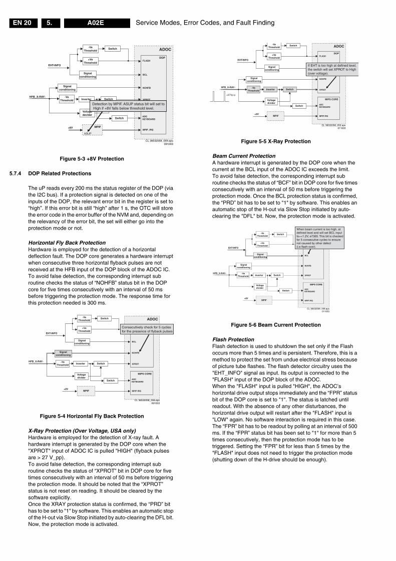
Service Modes, Error Codes, and Fault FindingEN 20 A02E5.
Figure 5-3 +8V Protection
5.7.4 DOP Related Protections
The uP reads every 200 ms the status register of the DOP (via the I2C bus). If a protection signal is detected on one of the inputs of the DOP, the relevant error bit in the register is set to “high”. If this error bit is still “high” after 1 s, the OTC will store the error code in the error buffer of the NVM and, depending on the relevancy of the error bit, the set will either go into the protection mode or not.
Horizontal Fly Back ProtectionHardware is employed for the detection of a horizontal deflection fault. The DOP core generates a hardware interrupt when consecutive three horizontal flyback pulses are not received at the HFB input of the DOP block of the ADOC IC. To avoid false detection, the corresponding interrupt sub routine checks the status of “NOHFB” status bit in the DOP core for five times consecutively with an interval of 50 ms before triggering the protection mode. The response time for this protection needed is 300 ms.
Figure 5-4 Horizontal Fly Back Protection
X-Ray Protection (Over Voltage, USA only)Hardware is employed for the detection of X-ray fault. A hardware interrupt is generated by the DOP core when the "XPROT" input of ADOC IC is pulled "HIGH" (flyback pulses are > 27 V_pp).To avoid false detection, the corresponding interrupt sub routine checks the status of “XPROT” bit in DOP core for five times consecutively with an interval of 50 ms before triggering the protection mode. It should be noted that the “XPROT” status is not reset on reading. It should be cleared by the software explicitly.Once the XRAY protection status is confirmed, the “PRD” bit has to be set to "1" by software. This enables an automatic stop of the H-out via Slow Stop initiated by auto-clearing the DFL bit. Now, the protection mode is activated.
Figure 5-5 X-Ray Protection
Beam Current ProtectionA hardware interrupt is generated by the DOP core when the current at the BCL input of the ADOC IC exceeds the limit. To avoid false detection, the corresponding interrupt sub routine checks the status of “BCF” bit in DOP core for five times consecutively with an interval of 50 ms before triggering the protection mode. Once the BCL protection status is confirmed, the “PRD” bit has to be set to "1" by software. This enables an automatic stop of the H-out via Slow Stop initiated by auto-clearing the "DFL" bit. Now, the protection mode is activated.
Figure 5-6 Beam Current Protection
Flash Protection Flash detection is used to shutdown the set only if the Flash occurs more than 5 times and is persistent. Therefore, this is a method to protect the set from undue electrical stress because of picture tube flashes. The flash detector circuitry uses the "EHT_INFO" signal as input. Its output is connected to the "FLASH" input of the DOP block of the ADOC. When the "FLASH" input is pulled "HIGH", the ADOC’s horizontal drive output stops immediately and the “FPR” status bit of the DOP core is set to "1". The status is latched until readout. With the absence of any other disturbances, the horizontal drive output will restart after the "FLASH" input is "LOW" again. No software interaction is required in this case. The “FPR” bit has to be readout by polling at an interval of 500 ms. If the “FPR” status bit has been set to "1" for more than 5 times consecutively, then the protection mode has to be triggered. Setting the “FPR” bit for less than 5 times by the "FLASH" input does not need to trigger the protection mode (shutting down of the H-drive should be enough).
FLASHDOP
ADOC
BCL
NOHFB
XPROT
ADCKEYBOARD
MPIF_IRQ
MIPS CORE
CL 36532058_059.eps091003
-VeThreshold
+VeThreshold
Switch
Switch
+8V
SwitchInverter
Voltagedevider
Signalconditioning
-VeThreshold
EHT-INFO
HFB_X-RAY-
Signalconditioning
MPIF
ASUP
Detection by MPIF. ASUP status bit will set to High if +8V falls below threshold level.
-VeThreshold
+VeThreshold
Signalconditioning
Switch
Switch
MPIF+8V
Voltagedivider
FLASHDOP
ADOC
BCL
NOHFB
XPROT
ADCKEYBOARD
MPIF IRQ
MIPS CORE
CL 36532058_056.eps091003
EHT-INFO
HFB_X-RAY-SwitchInverter
-VeThreshold
Consecutively check for 5 cyclesfor the presence of flyback pulses
Signalconditioning
-VeThreshold
+VeThreshold
Signalconditioning
Switch
Switch
MPIF+8V
Voltagedivider
Signalconditioning
FLASHDOP
ADOC
BCL
NOHFB
XPROT
ADCKEYBOARD
MPIF IRQ
MIPS CORE
CL 36532058_055.eps011003
EHT-INFO
HFB_X-RAY-SwitchInverter
-VeThreshold
>27Vp-p
If EHT is too high at defined level, the switch will set XPROT to High (over voltage).
-VeThreshold
+VeThreshold
Switch
Switch
MPIF+8V
SwitchInverter
Voltagedivider
Signalconditioning
-VeThreshold
FLASHDOP
ADOC
BCL
NOHFB
XPROT
ADCKEYBOARD
MPIF IRQ
MIPS CORE
CL 36532058_058.eps011003
EHT-INFO
HFB_X-RAY-
Signalconditioning
When beam current is too high, atdefined level and will set BCL input to=<1.2V, e7365. This bit is checked for 5 consecutive cycles to ensure not caused by other defect(i.e flash-over).
Service Modes, Error Codes, and Fault Finding EN 21A02E 5.
Figure 5-7 Flash Protection
5.7.5 Hardware Related Protections
Due to the architecture (read “hot” deflection), some protections cannot be sensed by the microprocessor. These protections will lead to a protection on set level (Standby mode and blinking LED).
Arc Protection If there are “open” connections (e.g. bad solder joints) in the high-energy deflection circuitry, this can lead to damaging effects (read: fire). For that reason, the E/W current is sensed (via 3479//3480). If this current becomes too high, the “thyristor” circuit (TS7653 and TS7654) is triggered. TS7442 is switched “on” and TS7443 is forced into conduction. The “SUP-ENABLE” signal is shorted now to ground level, which will force the Main Power Supply to Standby mode. This prevents further arcing.
Vertical Protection If the frame stage generates no pulses, TS7641 will block. TS7443 is now switched “on”, which will lead to Standby mode. Therefore, in normal operation condition, TS7641 and TS7652 are conducting, while TS7443 is blocked.
EW protectionSeveral faults in the defection circuit can cause excessive currents through MOSFET 7480. The temperature of this device can become too high, causing an unsafe situation. The power supply is shut down in the above-mentioned way.Caution: All hardware deflection protections can be disabled by interrupting R3403 on the LSP. However, be careful: unsafe situations (heat) can occur or the picture tube can be destroyed.
Bridge coil protectionAccording safety regulations, every coil may be short-circuited. By doing this in the secondary winding of coil L5422, high currents will flow in the winding. With no safety circuit, the coil will begin to burn soon. This is sensed via the “EW” signal going to the base of TS7652 (via R3495 and D6499). In a normal situation, the voltage on C2498 (diagram A4) is high and TS7652 is conducting. When bridge coil 5422 (diagram A3) is short circuited, the voltage on C2498 changes to low, which will block TS7652. In this case, also TS7641 will block and the voltage on 2642 will rise until TS7443 is forced in conduction. The “SUP-ENABLE” signal (in normal operating condition -20 V) is shorted now to ground level, which will force the Main Power Supply to Standby mode.Note: Maximum EW width settings can also cause a protection.
5.8 Repair tips
5.8.1 Miscellaneous
The relay you hear when you switch the set “on” (from Standby or via the mains switch), is from the degaussing circuitry. It is not used for switching the Power Supply (as done in the MG-chassis).• Take care not to touch the “hot” heatsink while
disconnecting the SSP, despite the fact that the mains cord is out of the mains socket. There still can be an annoying rest-voltage on the heatsink for a short while, because the discharge resistors 3502 and 3503 (on the LSP between hot and cold part) are not stuffed for Europe. Instead, discharge resistors 3066 and 3057 on the Mains Switch panel are used, but because they are located before the Mains switch, they only discharge when this switch is “on”. Advice: when you want to disconnect the SSP, first disconnect the Mains cord, but keep the Mains Switch in the “on” position.
• Where the circuitry was too “crowded” for service printing, you can find the correct location on the “test point overviews” in this manual.
• A very large part of the LSP is “hot”, such as:– The primary part of the Standby Supply.– The whole Main supply (except for the secondary
Audio supply).– And the complete deflection circuitry (so notice that the
deflection coil is hot!).
5.8.2 Start-up/Shut-down Sequence
For a detailed description, see chapter 9 " Circuit Descriptions, Abbreviation List, and IC Data Sheets".
5.8.3 ComPair
This chassis does not have an IR transmitting LED (as in MG-sets). Therefore, a “Service” (ComPair) connector is implemented at the rear side of the set, which is directly accessible. In addition to this, there is also a blinking LED procedure to show the contents of the error buffer. When you use ComPair, you have the possibility to activate a “stepwise start-up” mode. With this mode, you can initiate the start-up sequence step by step. This also means that in certain steps, some protections are not activated. This is sometimes very convenient during repair.
5.8.4 Protections
Activating SDM via the “service pads” will overrule the processor-controlled protections, but not the hardware protections. Caution: When doing this, the service technician must know what he is doing, as it could lead to damaging the set. The “ARC”- and/or “BRIDGECOIL” protection are hardly ever triggered, however: • When you suspect the “ARC” protection, look for bad
solder joints and smell. By interrupting resistor 3497, this protection is disabled (special attention needed!).
• When you suspect the “BRIDGECOIL” protection, which can also be due to a too wide picture amplitude, shorten G and S of the E/W MOSFET 7480. This will disable the protection. You will now have minimal horizontal amplitude. Re-align the horizontal amplitude in the SAM menu and remove the G/S short of TS7480.
FLASHDOP
ADOC
BCL
NOHFB
XPROT
ADCKEYBOARD
MPIF_IRQ
MIPS CORE
CL 36532058_054.eps011003
-VeThreshold
+VeThreshold
Switch
Switch
MPIF+8V
SwitchInverter
Voltagedivider
Signalconditioning
-VeThreshold
EHT-INFO
HFB_X-RAY-
Signalconditioning
Service Modes, Error Codes, and Fault FindingEN 22 A02E5.
5.8.5 Main Supply
1. Replace FET 7504 and zener 6505.2. Disconnect the SSP panel.3. Short B and E of TS7529, in order to put the Main Supply
in “on”-mode (TS7529 is blocking then). Caution: To prevent that R3403 and TS7443 will be damaged, first disable the HW-protection of the deflection circuit. Therefore, short-circuit C2642 on the LSP (diagram A4).
4. Attach a load of 500 Ω to the V_BAT capacitor C2515 (the supply can not work without a minimum load).
5. Use a variac, and slowly increase the V_MAINS. Measure over sensing resistors R3514//15, if a nice sawtooth voltage becomes available.
6. Also, measure the V_BAT. This may never exceed +141 V. If it does, there is something wrong in the feedback circuitry (e.g. regulator 7506).
Note: Be careful when measuring on the gate of FET TS7504. This circuitry is very high ohmic and can easily be damaged
(first connect ground to measuring equipment, than measure the gate).
5.8.6 Frame Deflection
Caution: When the Frame Deflection circuitry is suspected, one must be careful. Because there is a DC-voltage on the frame deflection, the beam current could damage the CRT neck, leading to a defective CRT. To prevent this from happening, you must:1. Interrupt the resistors 3403 and 3404 on the CRT panel
(diagram F), in order to remove the “filament” voltage from the tube (no beam current, so no chance of destroying the CRT).
2. Interrupt resistor 3403 on the LSP (diagram A4) to disable the “SUP-ENABLE” line.
3. Measure with a multi-meter, or better with an oscilloscope, the functionality of the Frame stage.
4. After you have found the cause, exchange the defective component (e.g. TDA8177), and re-solder the interrupted resistors.
Table 5-3 Repair tips
5.9 Software Downloading
In this chassis, you can upgrade the software via ComPair. You can find more information on how this procedure works in the ComPair file. It is possible that not all sets are equipped with the hardware, needed to make software upgrading
possible. To speed up the programming process the firmware of the ComPair interface can be upgraded. See paragraph “How To Order” for the order numbers.
Phenomenon Possible Cause Repair tip
No picture, no LED. Standby Supply defective. Measure circuitry (see diagram A2). Start at test-point A19.When the Mains switch is "on", this voltage must always be available.
No picture, LED blinking at 3 Hz.
Set is in protection due to various causes. For error codes see error-code list.
You have no picture, so: read the error buffer via ComPair (error buffer is accessible when set is in protection, ComPair-file will guide you to this). Read the blinking LED information via standard remote command mute-06250x-ok. Or you read the error code sequence via standard remote command mute-062500-ok. When you have found the error, check the circuitry related to the supply voltage and I2C-communication or the circuitry that triggers the protection.
No picture, LED blinking with code 8-8-8-etc or 9-9-9-etc.
No communication on slow I2C- or fast I2C-bus.
As processor cannot communicate with one of the 2 busses it the standby-LED spontaneously starts blinking 8-8-8-etc or 9-9-9-etc... If in the error buffer somewhere is an error 8 or 9, these will have the highest priority starting the mentioned blinking. Measure dependent of the error on the I2C-bus which device is loading the bus (use the I2C-overview)
No picture, LED blinking with code 13-13-13-etc.
No communication on NVM-I2C bus to the uP.
As the uP cannot communicate with the NVM I2C bus, it spontaneously starts blinking 13-13-13-etc. Note: when there is no access to the NVM, a lot of picture setting can go wrong.
No picture, no sound. Set is making audible squeaking sound
Supply is possibly in hiccup-mode, which is audible via a squeaking supply transformer.
Possible causes: V_BAT is shorted (caused by short circuited line transistor 7421), the sound winding is shorted (amplifier is shorting the power supply lines), or D6514 is shorted (due to a too high V_BAT). Remove excessive load, to see what causes the failure, or check feedback circuit. See repair tip "Main Power Supply" (supply needs a minimal load).
No picture, no sound. Front LED works fine
Supply does not work correctly. If e.g. V_BAT is only about 90 V, it is possible that the regulator IC (7506) is defective.
No RC-reception. Front LED does not echo RC-commands.
uP circuitry or RC-receiver is defective.
In case the set does react on a local keyboard operation, you must check the RC-receiver circuitry (diagram J).
Relay (degaussing) is not audible, when set is switched from "off" or "standby" to "on".
uP is not working correctly. When line "DEGAUS" is low, the degaussing must be activated.
Check RESET-circuitry (IC7581 on diagram B11). Check the level on line "DEGAUS" when you switch the set "on". Signal must be low initially and go to high after approx. 12 s.
Picture is rotated. Rotation circuitry (if present) on diagram A5, or related supply to it, malfunctions.
Measure test points on diagram A5.
Picture is continuously switching "off" and "on", showing heavy "switch" spots (set does not go into protection).
200 V is missing on CRT panel. Probably a bad connection from LSP connector 1424 to CRT connector 1424 (diagram F), or an interruption of the 200 V supplies line (e.g. R3341 on circuit F1 is interrupted).
Picture is not sharp. Focus is possibly mis-aligned or SCAVEM-circuitry does not work correctly.
Re-align the "FOCUS" potmeter on the Line Output Transformer, or check the SCAVEM circuitry on the CRT-panel (diagram F). It is also possible that the DAF circuitry is defective (see diagram I). Check the V_dc values.
Picture is distorted. Check video-path in Service Default Mode.
Investigate whether there is an error code present in the error buffer. In case there is one, check the I2C-bus and/or supply lines (see overview supply lines). Measure and check signal path Tuner-MPIF-ADOC-RGB amplifier. In case it is a geometry issue, check on diagram A4 opto-coupler 7482, OpAmps 7440/7450 and the Frame circuitry alignments or a possible corrupted NVM (IC7525 on diagram B11).
No menu, no OSD. Probably a defective uP (ADOC).
No Teletext. IC7730 defective or not powered. Check circuitry around IC7730 on diagram B13.
Strange switch "off" behaviour
TS7445 possibly defective. Check, with a multi-meter, whether transistor TS7445 is well functioning. (diagram A3).
Various symptoms, due to missing local supply voltage.
An interrupted fuse, NFR-resistor or connection.
When no symptom or error code leads you to a specific circuitry, use the supply lines overview (see supply lines overview), for a quick scan of all supply lines.
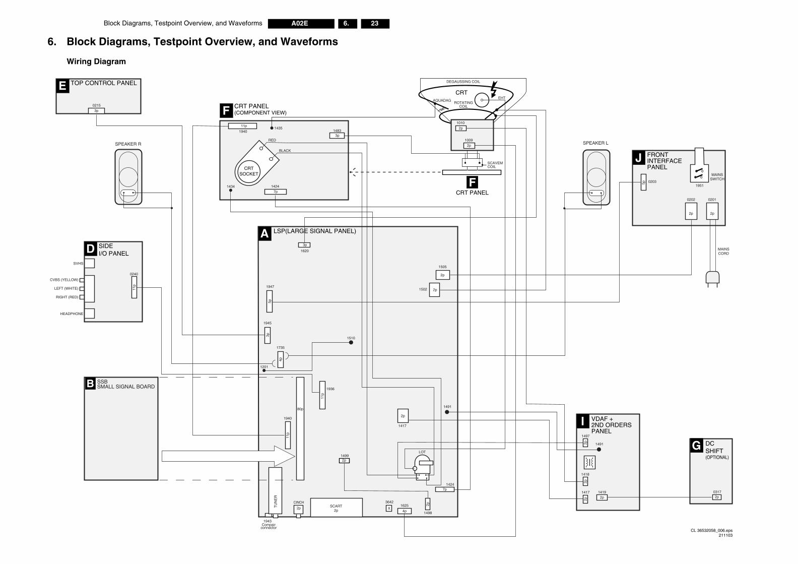
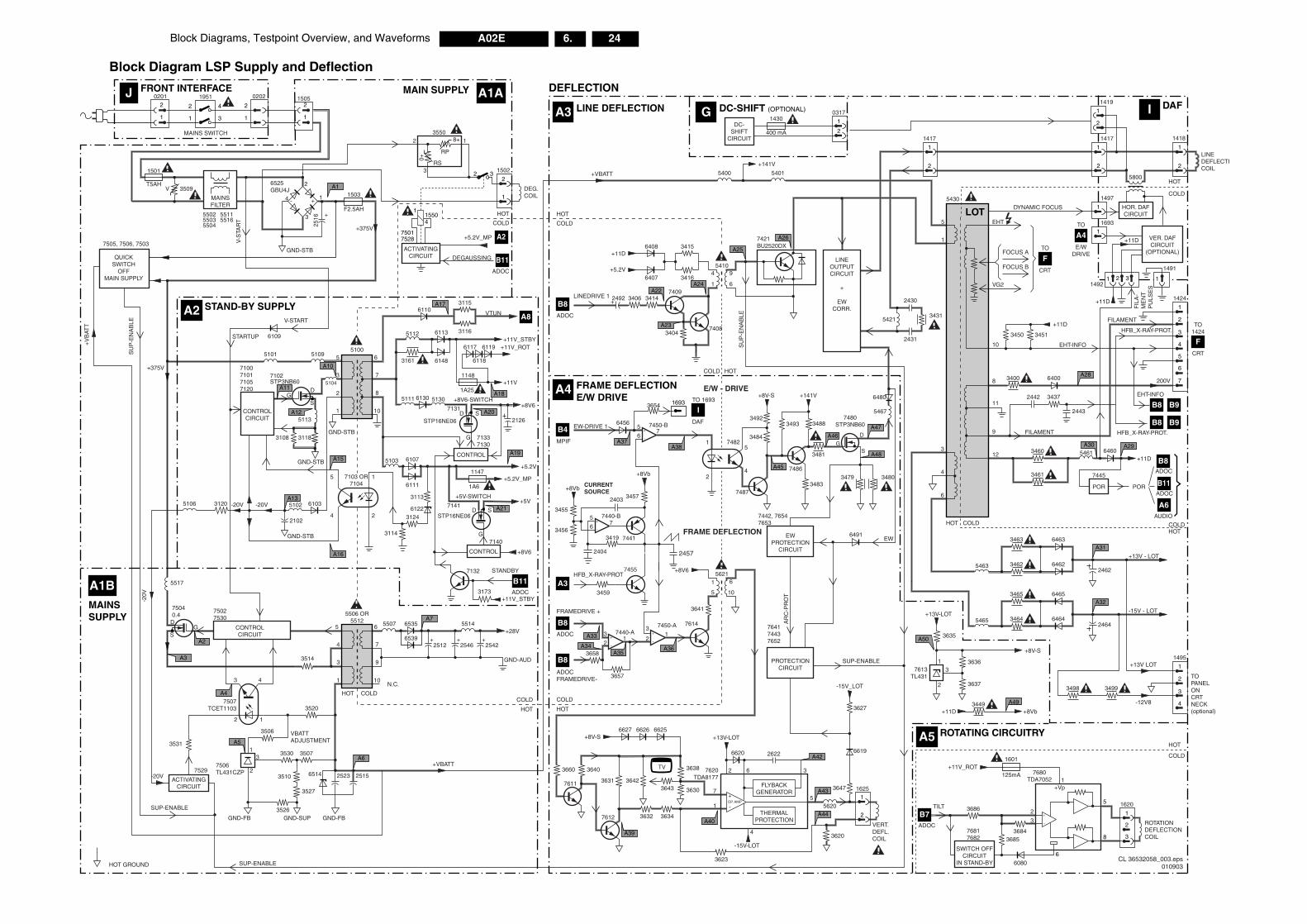
Block Diagrams, Testpoint Overview, and Waveforms 23A02E 6.
CL 36532058_006.eps211103
VDAF +2ND ORDERSPANEL
02031951
I
FRONTINTERFACEPANEL
J
1419
MAINSSWITCH
SPEAKER L
DCSHIFT(OPTIONAL)
0317
G
1417
1418
1497
1491
0201
MAINSCORD
2p
0202
2p 2p
5p
2p2p
2p2p
11
B
1491
16253642
1417
1940
TU
NE
R
1943Compair
connector
LOT1499
TU
NE
R
1498
1424
4pX
2p
80p
SCART2p
CINCH
2p
7p
11p
2p
2p
6. Block Diagrams, Testpoint Overview, and Waveforms
Wiring Diagram
SIDE I/O PANELD
0240
CRT PANEL(COMPONENT VIEW)F
TOP CONTROL PANELE
A
1424
BLACK
RED
EHT
1483
1434
14351940
HEADPHONE
SVHS
RIGHT (RED)
LEFT (WHITE)
CVBS (YELLOW)
0215
1502
1505
1735
1936
1201
SPEAKER R
CRT PANELF
SCAVEMCOIL
AQUADAG
DEGAUSSING COIL
ROTATINGCOIL
CRT
LSP(LARGE SIGNAL PANEL)
1945
1947
1620
1010
1009
1510
CRTSOCKET
7p
3p
11p
3p
3p
2p
2p
2p
2p
p
4p
3p5p
11p
SSBSMALL SIGNAL BOARDB
24A02E 6.Block Diagrams, Testpoint Overview, and Waveforms
CL 36532058_003.eps010903
DAF
LOT
I
ROTATING CIRCUITRYA5
F
2
1
A28
A29
A31
A3
3431
2430
2431
6080
1417
EHT
FOCUS B
DYNAMIC FOCUS
FILAMENT
HFB_X-RAY-PROT.
HFB_X-RAY-PROT.
200V
VG2
10
8
11
9
3
4
6
12
3450 3451
1491
+11D
+11D
+11D
1492
EHT-INFO
EHT-INFO
+11D
PORPOR
7445
FILAMENT
TO
CRT
A4TO
E/WDRIVE
F
A6
TO1424
CRT
5
5430
HOT COLD COLD
AUDIO
B8
B8 B9
B8 B9
ADOC
B11ADOC
HOT
COLD
HOT
1
2
1
1417 1418
1497
5800
1693
2
1
1
1
2
1
1419
3
1
5
8
6
2 ROTATIONDEFLECTIONCOIL
1620
2
3
4
5
6
7
1
1424
2
1
3
FOCUS A
2
3
4
1
1495
TILT
ADOC
3400
3437
3460
3461
3462
3463
6462
6463
2462
+13V - LOT
+13V LOT
TOPANELONCRTNECK(optional)
-12V8
5463
6400
2442
2443
64605461
A32
2464
A36A353658
B7
3464
34993498
3686
3684
+Vp
+11V_ROT1601
125mA 7680TDA7052
3685
76817682
3465
3449
6464
6465
-15V - LOT
5465
SWITCH OFFCIRCUIT
IN STAND-BY
3514
COLD
HOR. DAFCIRCUIT
VER. DAFCIRCUIT
(OPTIONAL)
HOT
LINEDEFLECTICOIL
A30
A49
31 2 1
A50
+13V-LOT
3635
3636
+11D +8Vb
1
2
37613TL431
3637
+8V-S
FIL
A-
ME
NT
PU
LSE
S
A43
A44
A426620
HOT
HOT
65143510
3527
3526
2523 2515
COLDCOLD
HOT
COLD
2
1
VERT.DEFL.COIL
1625
3627
6619
36477611
7
3
2622
5
4
-15V-LOT
62
OP. AMP1
+13V-LOT
-15V_LOT
B8ADOCFRAMEDRIVE-
3660+VBATT
3640
3631
+8V-S6627 6626 6625
36423643
TV
3630
3632
3623
3620
5620
3634
FLYBACKGENERATOR
3638 7620TDA8177
7612A40
A39
36573
2
4
1
13
2
3506
7507TCET1103
3507
3520
VBATTADJUSTMENT
3530
7506TL431CZP
3531
PROTECTIONCIRCUIT
THERMALPROTECTION
A6
GND-AUD
GND-FB
HOT GROUND
GND-SUPGND-FB
7529-20V
SUP-ENABLE
9
10N.C.
3
1
ACTIVATINGCIRCUIT
A4
SUP-ENABLE
A5
SUP-ENABLE
Block Diagram LSP Supply and Deflection
LINE DEFLECTIONA3 DC-SHIFT (OPTIONAL)G
MAIN SUPPLY A1AFRONT INTERFACEJ
FRAME DEFLECTIONE/W DRIVE
A4
STAND-BY SUPPLYA2
MAINSSUPPLY
A1B
B8
B11
A15
A10
A11
A13
A16
A2
A45
A46A47
A25
A26
A24A22
A12
A23
A20
6408+11D
+5.2V
+5.2V_MP
DEGAUSSING
MAINS SWITCH
6407
6110
6117
6118
6119
3115
3116
+8V6-SWITCH
71337130
2126
7131
STP16NE06
STP16NE06
7140
7132
3173
7141
CONTROL
6113
1148
5112
3161
5111 51306130
6148
1A25
3415
945410
7421BU2520DX
+141V
LINEOUTPUTCIRCUIT
+
EWCORR.
5421
613416
7408
SU
P-E
NA
BLE
COLD HOT
3404
7409341434062492
+LINEDRIVE 1
EW-DRIVE 1
MPIF
VTUN
57
1
2
5
+8V-S +141V
7482
3492
3484
3493 3488
74873483
EWPROTECTION
CIRCUIT
3481
5467
6480
7480STP3NB60
7486
E/W - DRIVE
FRAME DEFLECTION
4
7450-B
3654
6456
6
+VBATT 5400
HOT
COLD
ADOC
HOT
ADOC
COLD
6
5
5621
7614
3641
10
1
2
1
0317
1
22
1
41550
75017528
3
DEG.COIL
1502
B4DAF
TO 1693
I
A8
31
7450-A
2
57
3455
34572403
7441
3459
7455
+8Vb
AR
C-P
RO
T
+8Vb
+8V6
655100
7103 OR7104
7
8
10
3
61075103
6111
3113
6122
+11V_STBY+11V_ROT
+11V
+5.2V
+5V
+5.2V_MP
+8V6
+8V6
+11V_STBY
6103
6109
-20V 510231205106
5517
2102
2
1
3456
2404
3419
7440-B
CURRENTSOURCE
6
HFB_X-RAY-PROT
A3
FRAMEDRIVE +
B11ADOC
STANDBY
ADOC
B8
3479
6491EW
7442, 76547653
+V
BAT
T
764174437652
3480
STARTUP
V-START
+375V
SU
P-E
NA
BLE
51095101
3509
1501
RP
RS3
2 13550
8+
0+
T5AHV
MAINSFILTER
ACTIVATINGCIRCUIT
550255035504
55115516
A37
A33 31
7440-A
2
5
3108 3118
GND-STB
GND-STB
GND-STB
5113
4
1
2
D
SG
D
G
S
A21
+5V-SWITCH
CONTROL
3114
3124
+375V
-20V
-20V
A76535
6539
5507 5514
2512+
6
5506 OR5512
75027530
75040.4
7
5
4
+28V
2542+
2546+
V-S
TAR
T
D
G
S
CONTROLCIRCUIT
CONTROLCIRCUIT
D
71027100710171057120
STP3NB60
GS
DG
S
1147
1A6
DC-SHIFT
CIRCUIT
A18
A19
A17
A48
A34
A38
2457
DEFLECTION
5401
1430
400 mA
1693
5104
7505, 7506, 7503
QUICKSWITCH
OFFMAIN SUPPLY
A11503
F2.5AH
2516
GND-STB
6525GBU4J
2
1
3
+
+
-4
A2
1
20201
1
21505
1
2
3
4
1951
1
2
0202
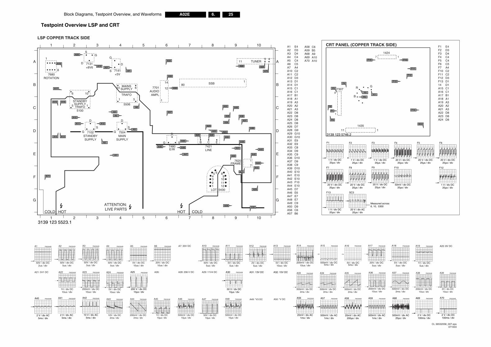
Block Diagrams, Testpoint Overview, and Waveforms 25A02E 6.
A1 PM3394B A2 PM3394B A3 PM3394B A4 PM3394B A5 PM3394B A6 A7: 33V DC A20: 8V DCPM3394B A10 PM3394B A11 PM3394B A12 PM3394B A13 PM3394B A14 PM3394B PM3394B PM3394B A17
20V / div DC5us / div
PM3394B A18
5V / div DC5us / div
PM3394B A19
1V / div DC5us / div
PM3394B
PM3394B
A16
5V / div DC5ms / div
A36
200mV / div DC10us / div
PM3394B A37
500mV / div DC2ms / div
PM3394B A38
200mV / div DC10us / div
PM3394B A39
2V / div DC10us / div
PM3394B
PM3394BPM3394B PM3394B PM3394B
DCiv
F2
Measured across 6, 10, 5300
1 V / div DC20µs / div
F3
1 V / div DC20µs / div
F4
20 V / div DC20µs / div
F5
20 V / div DC20µs / div
F6
20 V / div DC20µs / div
DCiv
F8
20 V / div DC20µs / div
F9
20 V / div DC20µs / div
F10
50mV / div DC20µs / div
A15
A35
500mV / div DC2ms / div
PM3394B
A58
20mV / div AC200µs / div
A59
500mV / div AC1ms / div
A68
500mV / div AC20µs / div
A69
2 V / div DC100ms / div
A70
2 V / div DC100ms / div
CL 36532058_007.eps071003
1424
1435
307
F1F2F3F4F5F6F7F10F11F12F1314A15A16A17A18A19A20A21A22A23A24
E4D3D4C4C4C5A4C2C2D3D1D1C1C1B1A1A3A2A3D8D8D8
ANEL (COPPER TRACK SIDE)
11 1
B
GR
F8
F11
F14
F13
F157 1
F9
F12
F7
SC3
F10
F4
F12
1 V / div DC20µs / div
DCiv
SC3
20 V / div AC20µs / div
3 5746.2
50V / div DC2us / div
50V / div DC5us / div
50V / div DC5us / div
PM3394B PM3394B PM3394B
50V / div DC5us / div
5V / div DC10us / div
A28: 206 V DCA26: A29: 11V4 DCA21: 5V1 DC
20V / div DC10us / div
50V / div DC5us / div
5V / div DC5us / div
PM3394B
2V / div DC5us / div
5V / div DC10us / div
200mV / div DC10us / div
A22
1V / div DC10us / div
PM3394B A23
200mV / div DC10us / div
PM3394B A24
5V / div DC10us / div
PM3394B PM3394B A33
500mV / div DC2ms / div
PM3394B
A43
10V / div DC2ms / div
PM3394B A44
200mV / div DC2ms / div
PM3394B A45
1V / div DC10µs / div
PM3394B A47
50V / div DC10µs / div
PM3394BA46
500mV / div DC10µs / div
PM3394B A48 A49: *V3 DC A50: *V DC
500mV / div DC10µs / div
PM3394B PM3394B PM3394B
500mV / div DC5ms / div
A25
200 V / div DC10µs / div
A30 A31: 13V DC A32: 15V DC
50 V / div DC10µs / div
A40
2 V / div AC5ms / div
A41
2 V / div AC5ms / div
A42
10 V / div AC5ms / div
A34
500mV / div DC2ms / div
PM3394B
A56
20mV / div AC1ms / div
A57
500mV / div AC1ms / div
Testpoint Overview LSP and CRT
F1
1 V / div 20µs / d
F7
20 V / div20µs / d
A7
A20
7131+8V6
GS
DA21
7141+5V
S
D
G
A19
LSP COPPER TRACK SIDE
SSBMAINS
SUPPLY
TRAFO
5506
7
TUNER
ECB
1
7
7421LINE
7480E/W
7620FRAME
123
12LOT 5430
1110
4 95 86
80
11
1
1
8
A32
A43
A49A33
A37
A36
A35
A69
A34
A38
A23
A59
A57
A56
A40
A15 A16
A71
A29
A13
A2
A6
A28
A46
A45
A44
A42
A68
A48
A47
A3
COLDHOTCOLD HOT
ATTENTION:LIVE PARTS
7504MAIN
SUPPLY
S
D
G
7701AUDIOAMPL
S
D
G
45
7680ROTATION
51
610
1
14
12
STANDBYSUPPLYTRAFO
5100
15
106
A10
A11
A5
A12
A1
A4
A58
7102STANDBYSUPPLY
S
D
G
A1A2A3A4A5A6A7A10A11A12A13A14A15A16A17A18A19A20A21A22A23A24A25A26A28A29A30A31A32A33A34A35A36A37A38A39A40A41A42A43A44A45A46A47A48A49A50A56A57
E4D3D4C4C4C5A4C2C2D3D1D1C1C1B1A1A3A2A3D8D8D8D8D7G9G10G10E9E9C8D9C9D10D9C9D10E10E10E10F10E10D7E6E7E7C9D9C6B6
A24A22
A17
A14
A
1 2 3 4 5 6 7 8 9 10
B
C
D
E
F
G
A
B
C
D
E
F
G
1 2 3 4 5 6 7 8 9 10
A58A59A68A69A70
C6B5A9A10A10
CRT P
A18
A30
A41
A31
A50
A39
A26A25
A70
9
1
F6
F3
F1
F5
F13
1 V / div 20µs / d
3139 123 5523.1
3139 12
26A02E 6.Block Diagrams, Testpoint Overview, and Waveforms
$)* , -.
:
0<
"
"
:
0<
:
0<
4:
$74!
$74"
!
"
$74!
$74"
!
"
$74!
$74"
!
"
"
020=
080:
'
7 ?>
'
'
'
'
'
'
4%%(7!%7#
$74!
$74"
!
"
$74!
$74"
!
"
$74!
$74"
!
"
> %"$(
> %
$
02(
)8$
0)
$
8:
"
"
"
$
$
$$
!$
!
7 ?>
'
'
'
$% !
$% 7#
% 7#
% 7#
$% 7#
7#
$7#
#$ %&
#$%&
#$%&
$/ (" $/
?
? !
?7#
?%("
?$
%$
(" #""6
? @ 7!$7
3$
'
.B
$)C,
4
$ %#%"7
$ %
(( 7!!
> "$(
>
''
'$$
$
#77# 7$
(7!7$7#
! $
@ $ $
#$7" 7!6
4%$%7#
7((%!
CL 36532058_010.eps210803
5 5
#7
("
$
!
!$
!
!$
$7!!
$ $7!!
!
!$
!
!$
$
'
'
>"
'
'
''
>">$
>">
6 4 $7!! 4
$7!!
$ $7!!
#%
#%$
$
6 4% !
4% !
% !
$% !
4%(7!7#
&!%6!
4!%#!
$!% !
% 7#
'
'
'
' $% 7#
% !
$% !
$% 7#
'
% 7#
#7 7#
#7$ 7#
$
$7:$
7:
4
::
&
$ 4
$7: 4
#%"" '>D
'
'
$7:
7:$
7:
::
"
7#
$7#
'
#7 7# #7#$$
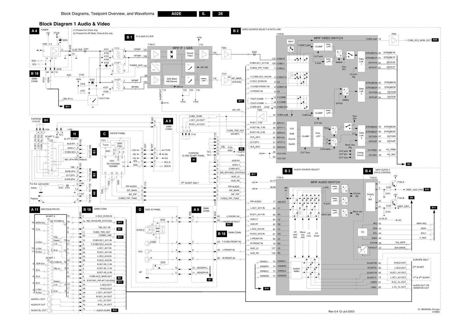
Block Diagram 1 Audio & Video
!"
#!$%&
'
%(!
#!$
$
/ (01)
( )2,
!!
!"
!!
&
'
'
"
3
4
4
4
456
456
67(4
7(4
$5"5
&5656
45"5#
$5"5
&5656
45"5#
6#
$&4
8)
90:8;
(" "
("
("
4% !
4%""%#!
6 4% !
% >!
6 4 $7!!
$7!!
67#7(4
7#7(4
$% !
&!%6!
4!%#!
$"$ >
&6 >
4"4 >
4
("
(" / '
'
'
'
'
!
( 3
$
$
(" #
""#7
% !
$% !
% !
#
#$
'
>
((
7!! 7 "!
'
'
'
55
):
"
4
4%$%7#
%""
'
7 7#$ @ !A
#7 7#$
@ ? $
'
'
6
?5"" "!
4
$7!!
$7!
4
4%""%#!
%(!
%""
4%$$
% 7#
> >
>
#$
#
""#7
>$%#
4%""%#!
%(!
%""
""#7
)?
0.:)
)2.:
'
$
""5?
'
")): C ;0 .B
")): C "(.:0 ;0 @ # .B
%"!
$ $ 7!6
#!
'
((
7!!
((
7!!
#!
$% 7#
4
75 $7(
7 $ $ "!
&
#%
#%$
'
!
'
4:4
% >!
>$$%#
!"#57#"# (( 7!!
4!
$
(7!7:65 4
'
$
4%)%7:
4
7 $ $
74
75 $7(
7
4
7'4
$"$ >
&6 >
4"4 >
#$
#
>$::
% 7:
$% 7:
!,,
1:, 9C)
8:0*)
"0*)
'
7
7
!,,
!,,
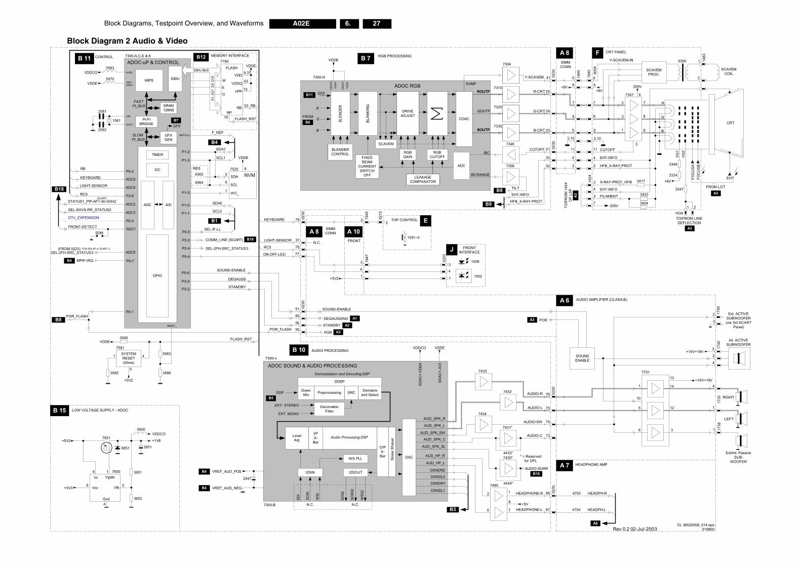
Block Diagrams, Testpoint Overview, and Waveforms 27A02E 6.
8
33
0
9
:
3
)
8
2
&
6
'
6
'#!
;6#*
()'77
/)#*7'
/7&,%;')
6
4
)'$7'044
'7! 4
3
044
3
9
:
00
4
0:4
0:4
8
3
9
:
00
4
) *!
#
'**
/)#*7'
/)7'(
7'(&
7' !')
4:
43
4
=96
<<=96
044
0
62
620
8
0 049
330
=0<6=0:6
$#
(&
.''7
034
4
4
#2/)
!7)
0
'(*
*&!
0
04
0
0
8
0
038
(#' !#7# @!&A
//
//!
< 039
0
# )#6
(&.''7
=0<6=0:6
)'$7' !#*
7!)#'*
6
<
:84
44
E0E0
=96
//'*
03:
)#6
(&.''7
@ )
A
403%;'),/7&
7#!*)
43
434
CL 36532058_014.eps210803
!
"
#$
%
&
#'()
'$
%
&
*+
(,-,.
(,-,
(,-,!
(,-,
(,-,!
(,/,
(,/,!
*!0
*0
*!
*
344
3405
345
3
38
34
<9
<3
(#'!
(#'.
(#'(
(#'
//'*
//'*!
67,(,'
3<80
6
6CD
6
6
2
9 0
< 8
4
<80
<8
=069=86
=6
3<8
!'. 6'!)2 (!; '
<<80
3& =86
349
<
0
3
9
67,(,*2
443
6'
8<
7
##*
. !!
!""
#
-#
.#
-
.
445
4445
<80
* *
5 F
C !
Block Diagram 2 Audio & Video
' '(* 1 (#' '#*234
34
#6
()
&!*
'*)'!
!-2
')'
30
3
)
2)
&)
()'77
'()
2'()
&'()
#6
()
2&
()'77
2&
2#*
&!*
'*)'!
!-2
')'
7#%
&
(*)
.#)/
'77
'()
&'()
#&
#&*2
' 2&
3/
3
40
8
4
0
/)#*7'
/7&,%;')
3<(#'
#&#(
09-&
##

27%
2*
2#'
#
$
)#
0890
89
890
-;&'
7'*)))
))(0,#7)8</>
!/6,))(
!#2/)*'
8
!
0
!0
'*'77!
!#7!!
'(**&!
!7/,))(
2(
)*&;
6' 6
#7#?
.
2
6
33: 6'*)'!
!7/,))(
)6,%*#'*
',!#* @)A
7,7
' 1 '*)'!
',7!/
3:
3
39
33
<
9
80
-;&'
8
!#2/)*'
)' '*)'!
0:0B4
7'*)
#*)7
4
0
09
#
'**
)*&;
2(#*2
'(**&!
'
(#' '#*2
'',7!/ 8
2& '#*2
@7' A
3EE 1 -
3
0:48
0
0=86
4
0
4
<
8
3
0
<
4
4
8
00
0
0
0
#7!-
%'()
%#*
@)A
7' 7/ #$ )
&#( &(
0008
7'*)
7'
6
'; #*)7
6
0
6
06
06
;6
&!*
&!*-#*2
6
6
:E3
6?4
7!/
),
7!/,)
7!/,)0<
6
6'
6
%6
883
889
388
.,
8
<
3
6
9
08
!
*6
6
34<
38<
)#!)
48<8
48<4
34
;)
)
@8A
3890
6
=86
89
8:
89
89<
0
8
4
08
&
&
&8
*
0:43
08
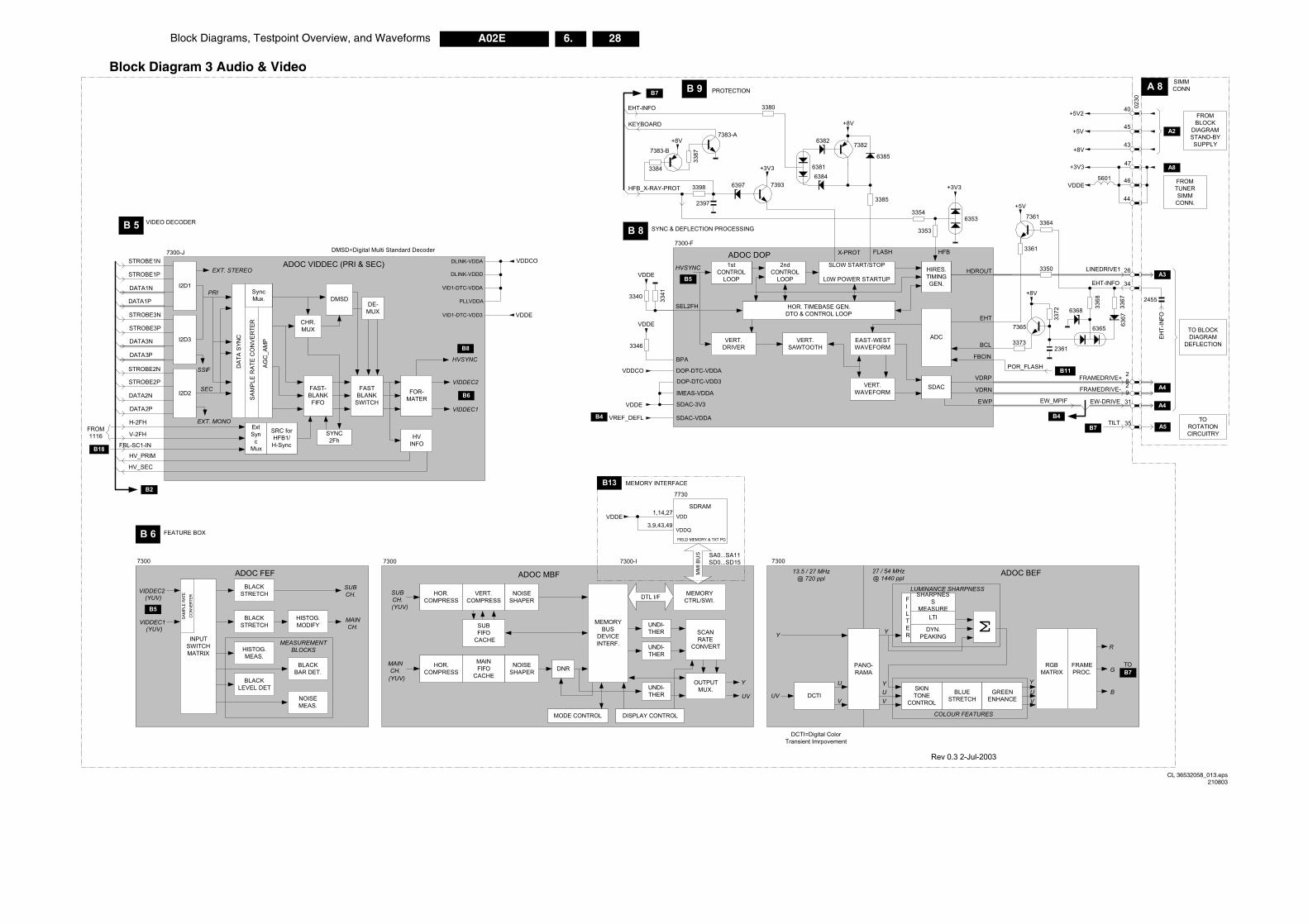
28A02E 6.Block Diagrams, Testpoint Overview, and Waveforms
(
(
(
(
!
001
02
0'
(
(
"
(
(
!
3
!
31
31
32
3
:
:
:1
0
:
2
4
!
(
:11
(
"
"
:'
:0
::
1
01
1
1:
3
00'
'01
'
1
"
10
'00:
0
002
32
'
31
0
CL 36532058_013.eps210803
"
#$
<=>=-? ))*
*?.,=.- @*A)@.-
Block Diagram 3 Audio & Video
!
"
#
$ % &
'
"
(
)* (
%
! +
! !
,-
(
%
! +
! !
,-
./
!
!
!
!
"
!
(
"
!
"
""
"
''
'2
'442 04'
02
02
021
32
#$
#$
#$
5-
6.
7
5
8)*
+
6.7
6.7
5
%
%
2
21
9:9'
949:9:4
" % (
0
:0
'
;
" % (
'
"
+!
1
+
"
' ''
:
:
2'
2:
'2
'232
"
02:
4'
<=>=-? -= -?./?*/ 7)/*
3
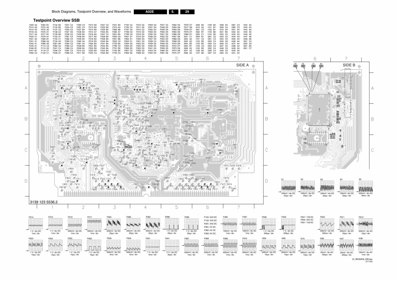
Block Diagrams, Testpoint Overview, and Waveforms 29A02E 6.
S1
100mV / div DC20µs / div
S4
100mV / div DC20µs / div
S3
100mV / div DC20µs / div
S2
100mV / div DC20µs / div
F509
1 V / div DC200µs / div
F601: 1V8 DCF650: 3V2 DCF651: 1V8 DC
F652
500mV / div DC500ns / div
F911
500mV / div DC20µs / div
F913
500mV / div AC10µs / div
I310
200mV / div DC10µs / div
I308
200mV / div DC10µs / div
C
I437
20mV / div AC200µs / div
I438
100mV / div AC1ms / div
I436
20mV / div AC500µs / div
S5
500mV / div DC50ns / div
CL 36532058_008.eps211103
S463 62 61 60
S3 S2 S1 SIDE B
F014
1 V / div DC1ms / div
F015
1 V / div DC1ms / div
F016
500mV / div DC1ms / div
F017
500mV / div DC1ms / div
F060
500mV / div DC20µs / div
F080
500mV / div DC20µs / div
F064
500mV / div DC20µs / div
F088
1 V / div DC20µs / div
F089
1 V / div DC20µs / div
F150: 3V2 DC
F152: 3V2 DC
F281: 3V2 DC
F381: 0V DC
F382: 0V DC
F383: 0V DC
F480
100mV / div AC1ms / div
F481
100mV / div AC1ms / div
F508
1 V / div DC500µs / div
F967
200mV / div AC1ms / div
F941
2 V / div DC20µs / div
F931
1 V / div DC5ms / div
F929
500mV / div DC5ms / div
F928
500mV / div DC5ms / div
F926
1 V / div DC10µs / div
F925
1 V / div DC10µs / div
F969
500mV / div AC1ms / div
F968
200mV / div AC1ms / div
F970
500mV / div AC1ms / div
F923
1 V / div DC10µs / div
F924
1 V / div DC10µs / div
I306
200mV / div D10µs / div
3139 123 5536.2
Testpoint Overview SSBI442 A4I443 A5I444 A5I445 A5I446 A5I447 A6I448 A6I501 C4I502 C6I601 B5I651 C7
I381 C3I382 C3I431 A4I432 A4I433 A3I434 A3I435 A4I436 A4I437 A4I438 A4I439 A3I440 A4I441 A4
I308 D4I309 C4I310 D4I341 B5I342 C5I343 C5I344 C5I345 C6I346 C5I347 C5I348 C5I349 C5I350 C5
I108 B2I151 B1I152 B1I153 B2I154 B2I281 C2I301 C4I302 C4I303 C4I304 C4I305 C4I306 C4I307 C4
I009 B2I010 A2I061 C2I062 B1I063 C1I064 B1I101 C2I102 B2I103 B2I104 C2I105 B2I106 B3I107 B2
F976 D7F977 D6F978 D7F979 D7F980 D7I001 C1I002 A2I003 A2I004 B2I005 B1I006 A2I007 A2I008 A2
F962 D5F963 D6F964 D6F965 D6F966 D6F967 D6F968 D6F969 D6F970 D6F972 D7F973 D6F974 D6F975 D7
F947 C5F948 D5F949 D5F950 D5F951 D5F952 D5F953 D5F955 D5F956 D5F958 D5F959 D5F960 D5F961 D6
F929 D3F931 D3F932 D3F933 D4F935 D3F936 D3F937 D3F938 C4F939 D2F940 D4F941 D4F943 D4F944 D4
F910 D2F911 D2F913 C2F915 D2F918 D2F919 D3F920 D3F921 D3F923 D3F924 D3F925 D3F926 D3F928 D3
F794 C5F795 C5F797 C6F798 C6F799 C6F901 D1F902 D1F903 D1F904 D2F905 D2F906 D2F907 C2F909 D2
F551 B3F570 A5F582 B6F584 A7F601 B5F650 C6F651 B6F652 C6F730 B5F790 C5F791 B5F792 B5F793 C5
F527 C2F532 B3F533 B4F534 B4F537 C4F538 B4F539 B4F540 B4F541 B4F542 B4F543 B4F544 B4F550 B3
F512 B3F513 B3F514 B3F515 A7F516 B4F517 B4F518 B4F519 B3F520 B4F521 B3F522 B3F523 B3F524 C4
F390 C3F391 C3F437 B4F438 B3F439 B4F448 B4F449 B4F480 A5F481 A5F508 B4F509 B4F510 A3F511 B3
F351 C4F354 C3F355 C5F357 D5F358 C5F381 C3F382 C4F383 C3F384 C3F385 C3F386 C4F387 C3F389 C3
F134 B2F135 B2F137 C2F138 C2F139 B2F150 A1F152 C1F159 A2F281 B4F282 A4F341 C4F346 C4F348 A1
F064 B1F074 A2F075 A2F076 A1F077 B1F078 A1F080 B1F088 A2F089 A2F114 C2F115 D2F116 C1F132 C1
1009 A2F014 A3F015 A3F016 A4F017 A4F020 C1F021 A2F041 A1F042 A1F045 A1F046 B1F047 B1F060 C2
2583
2582S5
SIDE A
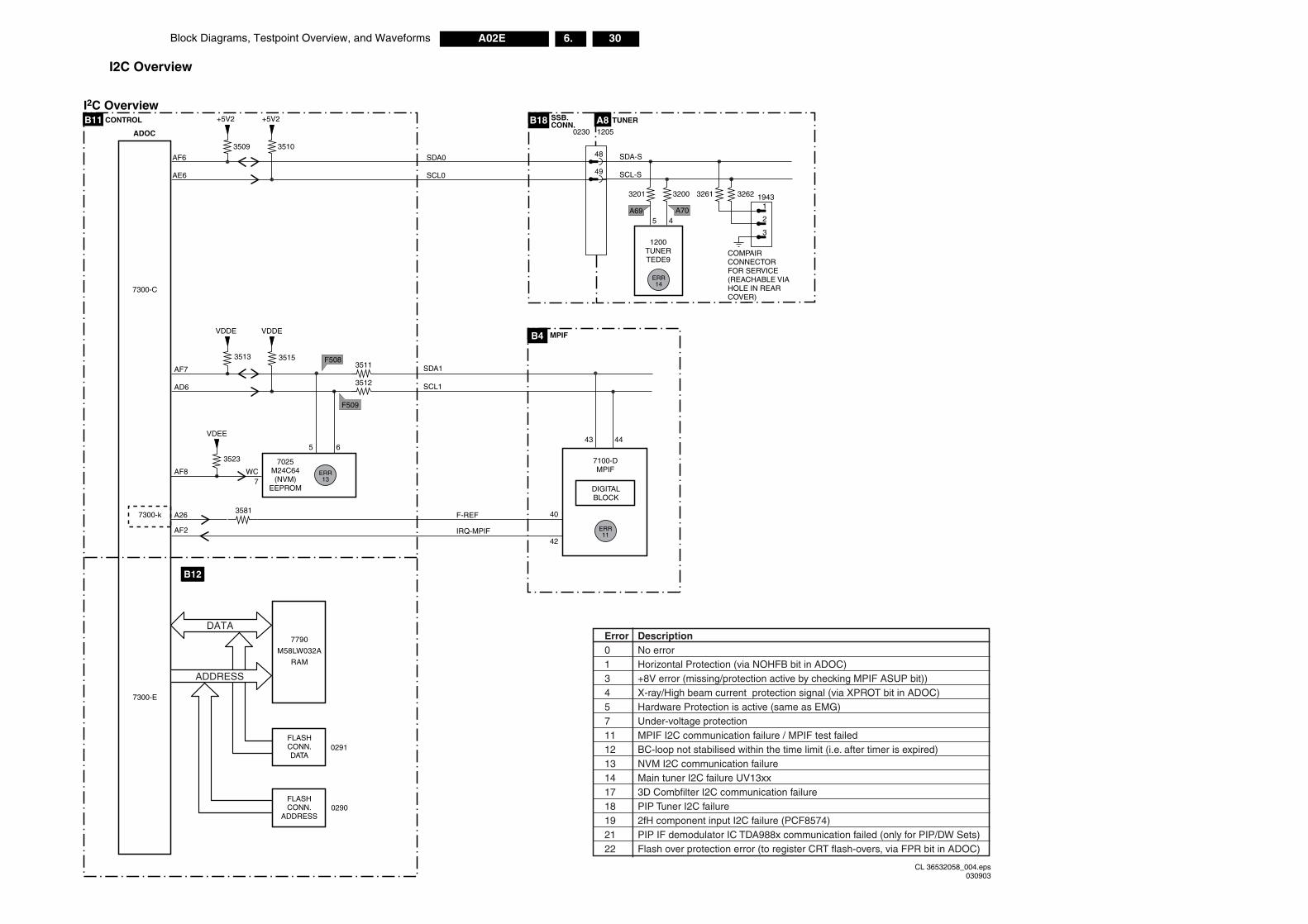
30A02E 6.Block Diagrams, Testpoint Overview, and Waveforms
M58LW032A
CL 36532058_004.eps030903
0 No error
P bit))n ADOC)
expired)
for PIP/DW Sets)FPR bit in ADOC)
0291
0290
RAM
FLASHCONN.DATA
FLASHCONN.
ADDRESS
ADDRESS
7300-E
1 Horizontal Protection (via NOHFB bit in ADOC)3 +8V error (missing/protection active by checking MPIF ASU4 X-ray/High beam current protection signal (via XPROT bit i5 Hardware Protection is active (same as EMG)7 Under-voltage protection11 MPIF I2C communication failure / MPIF test failed12 BC-loop not stabilised within the time limit (i.e. after timer is13 NVM I2C communication failure14 Main tuner I2C failure UV13xx17 3D Combfilter I2C communication failure18 PIP Tuner I2C failure19 2fH component input I2C failure (PCF8574)21 PIP IF demodulator IC TDA988x communication failed (only22 Flash over protection error (to register CRT flash-overs, via
I2C Overview
CONTROL
ADOC
TUNERA7SSB.CONN.B1
A69 A70
I2C Overview
SDA0
SCL0
AF6
7300-C
AE6
35113513
3523
3581
3515
SDA1
F-REF
IRQ-MPIF
SCL1
+5V2 +5V2
VDDE
VDEE
VDDE
3509 3510
AF7
3512AD6
AF8
A26
AF2
WC
B11
7025M24C64(NVM)
EEPROM
7790
ERR13
ERR14
ERR11
5
7
6
3201
5 4
3200 3261 3262
1200TUNERTEDE9
1205
SDA-S
SCL-S
0230
48
49
1
2
3
1943
COMPAIRCONNECTORFOR SERVICE(REACHABLE VIAHOLE IN REARCOVER)
A8B18
MPIFB1B4
F509
F508
DATA
B12
7100-DMPIF
43
40
42
44
DIGITALBLOCK
7300-k
Error Description
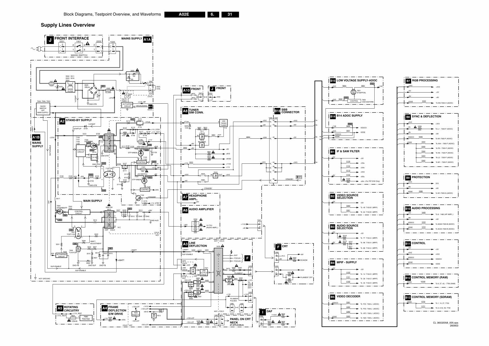
Block Diagrams, Testpoint Overview, and Waveforms 31A02E 6.
LINEDEFLECTIONA3
54301
ADJUSTMENT3531 A5
CRT
5283To N23 7300-J (ADOC)
To AF3 7300-J (ADOC)
To P23 7300-J (ADOC)
To F23 7300-J (ADOC)
VIDEO DECODER
O 5281
5282
5285
To 35 7100-D (MPIF)
To 28 7100-D (MPIF)
To 14 7100-D (MPIF)
+5V
MPIF - SUPPLY
+8V
5150
5151
5152
B13
To 3, 9 43, 49, 7730
To 1, 14, 27, 7730
CONTROL MEMORY (SDRAM)
VDDE
5731
5730
B11
+5V
CONTROL
+5V
+5V2+5V2
VDDCOVDDCO
VDEEVDDE
B10
To 8 - 7480 (HP AMPL.)
AUDIO PROCESSING
+5V
+8V+8v
To AD22-7300-B (ADOC)VDDCO
To AC22-7300-B (ADOC)VDDE
B12
To 9, 37, 43, - 7790 (RAM)
CONTROL MEMORY (RAM)
VDDE VDDE
VDDE
VDDCO
B14 ADOC SUPPLY
5600
5601
7650CS51033YDR8
LOW VOLTAGE SUPPLY-ADOC
+1V8
DDEDDCO
5654 5651
5659CONTROL
+5Vd
+5Vb
+5Va
+5V
IF & SAW FILTER
5135
5134
5102
5112
To 98 7100-A (MPIF)
To 88 7100-A (MPIF)
To 77 7100-A (MPIF)
+5V
AUDIO SOURCESELECTION
3018
3019 3010
3011
To 64 7100-B (MPIF)
To 49 7100-B (MPIF)
+5V
VIDEO SOURCESELECTION
5060
5061
+8Vc
+8Va3134
(For PIP D/W Only)
F601
7651STS5PF30L
F650
F651
5480
5452
5450
B9
3V3
PROTECTION
+3V3
+8V+8v
To W1-7300-G (ADOC)VDDE 3388
+8V+8v
+3V3+3V3
+5v
To M1-7300-F (ADOC)VDDCO 5342
B8
To AA4 - 7300-F (ADOC)
To R3 - 7300-F (ADOC)
To N4 - 7300-F (ADOC)
To L2 - 7300-F (ADOC)
To M1 - 7300-F (ADOC)
SYNC & DEFLECTION
VDDE
5345
3340
5344
5343
5342
To L1 - 7300-F (ADOC)
3358
B7
+3V3
RGB PROCESSING
+3V3
+8V+8v
+5V+5v
To W4-7300-H (ADOC)VDDE 5300
CL 36532058_005.eps260903
3
1
1492+11D +11D
FILAMENTPULSES
FILAMENT CRT
PANEL ON CRTNECK(IF APPLICABLE)
F
F
+VBATT
SUP-ENABLE
5400 5401+141V
+5V2
+11D
HOT COLD
LOT
COLDHOT
COLD
-15V-LOT
+13V-LOT
+13V-LOT
-15V-LOT
EW
LINEDRIVE
HOT
5
1
54107421
34656464
6465
3464
3400
3300
3404
3403
LINEOUTPUTSTAGE
9410
5465 3
3463
3499
6462
3461
12
9
6460+11DTO345034515441
6400
FOCUS 2
FOCUS 1
EHT
34605461
3462
3498
3635
5463
1485
6
FILAMENT 2
7
1424 1424
8
6463
3
1
3
1
FRAMEDEFLECTIONE/W DRIVE
A4
COLD HOT
3449
7620TDA8177
4
2
+11D+8Vb
+13V-LOT+13V-LOT
+8V-S
+141V
-15V-LOT
-15V-LOT
7813
2
7
11940
+8V
N.C.+8V
200V
SCAVEM6
1
1498 1499
+11D1
DAFI380911VDC
1492
3
1
3807 3808
+VBATT
1601
125mA
+11V_ROT+11V_ROT
1 7680TDA7052
ROTATINGCIRCUITRY
A5
65143510
3527
3526
2523 2515
+VBATT3
2
35073530
7506TL431CZP
A6
GND-FB
HOT GROUND
GND-SUPGND-FB
7529-20V
SUP-ENABLE
ACTIVATINGCIRCUIT
SUP-ENABLE
B5
VDDE
VDDC
B4
+5V
Supply Lines Overview
1
1947
6
1940
3941
3904
TUNERSIM CONN.A8
AUDIO AMPLIFIERA6
HEADPHONEAMPL.
A7
FRONTA10FRONTJ
VTUN 9
7.3
5901
6200-C33
1200TEDE9TUNER
SBBCONNECTORB18
1
0203
+5V2
43
40+5V2
+8V
+5VA
+3V3
+8V
1000
STANDBY
STANDBY
+3V3
2x
6x
8x
8x
4x
5x
+5V
+8V
+5V2
1205
45
44
+3V3OUTIN
+5VT
+8V
+8VS2
+11V5
+11V
+8VS
+8V
+8V
+11V
+5V
+5V2
5903
+5V
1+11V5
46
47
36
7910
9970
9972
OUTIN
7911L78L05
7912MC78M05
3907 3910
9909
9980
HOT COLD
3720
3721
3722
5904
5902
MAINS SUPPLY
STAND-BY SUPPLY
MAIN SUPPLY
A2
MAINSSUPPLY
A1B
A1A
B11
A15
A10
A11
A13
A16
A2
A12
A3
A20
+5.2V_MP
DEGAUSSING
6110
6117
6118
6119
3115
3116
+8V6-SWITCH
71337130
2126
7131
STP16NE06
STP16NE06
7140
7132
3173
7141
CONTROL
6113
1148
5112
3161
5111 51306130
6148
1A25
VTUN
HOT
ADOC
COLD
HOT COLD
HOT
COLD
1
22
1
41550
75017528
3
DEG.COIL
1502
655100
7103 OR7104
7
8
10
3
61075103
6111
3113
6122
+11V_STBY
+11V_ROT
+11V
+5.2V
+5V
+5.2V_MP
+8V6
+8V6
+11V_STBY
6103
6109
-20V 510231205106
5517
2102
2
1
STANDBY
+V
BAT
T
STARTUP
V-START
+375V
SU
P-E
NA
BLE
51095101
3509
1501
RP
RS3
2 13550
8+
0+
T5AHV
MAINSFILTER
ACTIVATINGCIRCUIT
550255035504
55115516
3
2
4
1
3506
7507TCET1103 3520
VBATT
5
3108 3118
GND-STB
GND-STB
GND-STB
5113
4
1
2
D
G
S
A21
+5V-SWITCH
CONTROL
3114
3124
+375V
-20V
-20V
A76535
6539
5507
3514
5514
2512+
GND-AUD
6
5506 OR5512
75027530
7504STP5NB60FP
7
9
10N.C.
5
4
3
1
+28V
+28V 13-7701(AUDIO AMPL.)
2542+
2546+
V-S
TAR
T
D
G
S
CONTROLCIRCUIT
CONTROLCIRCUIT
D
71027100710171057120
STP3NB60
GS
DG
S
1147
1A6
A4
A18
A19
A17
5104
7505, 7506, 7503
QUICKSWITCH
OFFMAIN SUPPLY
A11503
F2.5AH
2516
GND-STB
6525GBU4J
2
1
3
+
+
-4
FRONT INTERFACEJ
MAINS SWITCH
1
20201
1
21505
1
2
3
4
1951
1
2
0202
B11
B14
B15
+5V2
+3V3
+1V8
VV
+3V3
B1
+5V
B3
+5V
B2
+5V
+8V
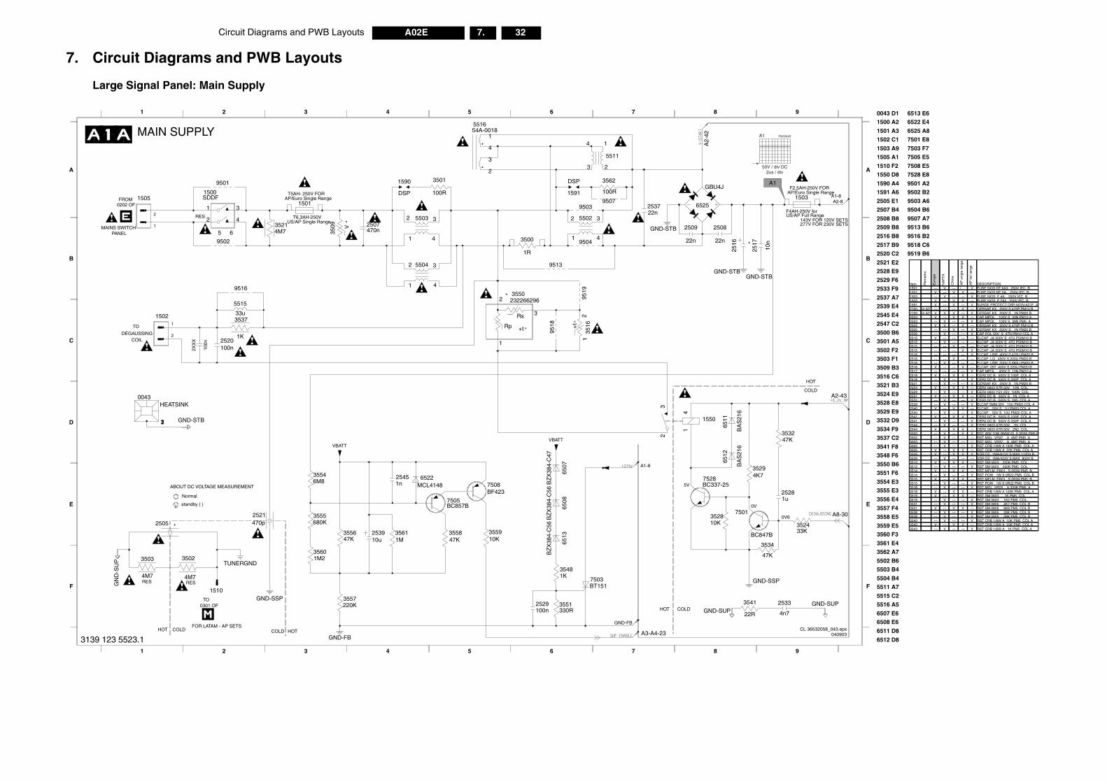
32A02E 7.Circuit Diagrams and PWB Layouts
A2-43
A8-30
HOT
COLD
A1-8
F4AH-250V for
F2,5AH-250V FORAP/Euro Single Range
US/AP Full Range143V FOR 120V SETS277V FOR 230V SETS
9
9
A
B
C
D
E
F
0043 D11500 A2
1501 A31502 C1
1503 A91505 A1
1510 F21550 D8
1590 A41591 A6
2505 E12507 B4
2508 B82509 B8
2516 B8
2517 B92520 C2
2521 E22528 E9
2529 F62533 F9
2537 A72539 E4
2545 E42547 C2
3500 B63501 A5
3502 F23503 F1
3509 B3
3516 C63521 B3
3524 E93528 E8
3529 E93532 D9
3534 F93537 C2
3541 F83548 F6
3550 B63551 F6
3554 E33555 E3
3556 E4
3557 F43558 E5
3559 E53560 F3
3561 E43562 A7
5502 B65503 B4
5504 B45511 A7
5515 C25516 A5
6507 E66508 E6
6511 D8
6512 D8
6513 E66522 E4
6525 A87501 E8
7503 F77505 E5
7508 E57528 E8
9501 A29502 B2
9503 A69504 B6
9507 A79513 B6
9516 B2
9518 C69519 B6
0V6
2533
10n
A1
47K3532
1503
STB
4n7
3560 BZ
GND-SUP
47K
352433K
47B
3534
1u
9
2528
D-SSP
A2-8
CL 36532058_043.eps040903
Item Rem
arks
Eur
ope
NA
FT
A
Chi
na
AP
sin
gle
rang
e
AP
full
rang
e
DESCRIPTION1501 --- V --- --
-
V FUSE 5X20 HT 6A3 250V IEC B1501 V --- V V --- FUSE 5X20 HT 5A 250V IEC B1503 --- V --- --- V FUSE 5X20 F 4A 250V IEC B1503 V --- V V --- FUSE 5X20 F 2A5 250V IEC B1591 V --- V --- V SURGE PROTECT DSP-501N-A21F A2100 in A2 --- --- --- V --- CERSAF KX 250V S 470P PM10 B2100 in A2 V V V --- V CERSAF KX 250V S 1N PM20 B2503 V --- V V --- CAP MPOL 100V S 33N PM10 A2503 --- V --- --- V CAP MPOL 100V S 39N PM5 A2505 V V --- V --- CERSAF KX 250V S 470P PM10 B2505 --- --- V --- V CERSAF KX 250V S 1N PM20 B2506 --- V --- --- V CAP POL 50V S 47N PM10 COL A2515 V --- --- --- --- ELCAP JA 200V S 47U P50M10 B2515 --- V --- --- --- ELCAP JA 200V S 47U P50M10 B2515 --- --- V --- --- ELCAP JA 200V S 47U P50M10 B2515 --- --- --- V V ELCAP JA 200V S 47U P50M10 B2516 --- --- --- --- V ELCAP USR 400V S 470U PM20 B2516 --- --- V --- --- ELCAP LQ 450V S 220U PM20 B2516 --- V --- --- --- ELCAP USR 200V S 680U PM20 B2516 V --- --- V --- ELCAP 057 400V S 220U PM20 B2517 --- --- --- --- V CAP MPOL 400V S 10N PM10 A2518 V --- V V --- CER2 DC B 500V S 100P COL A2518 --- V --- --- V CER2 DC B 500V S 330P COL A2521 --- V --- --- V CERSAF KX 250V S 1N PM20 B2524 V --- V V --- CER2 0603 X7R 50V 10N COL2529 --- V --- --- V CER2 0603 Y5V 25V 100N COL2531 V --- V V --- CER2 DC B 500V S 1N COL A2531 --- V --- --- V CER2 DC B 500V S 1N5 COL A2539 --- V --- --- V ELCAP 5MM 35V 10U PM20 COL A2540 V --- V V --- ELCAP 50V S 1U PM20 COL A2540 --- V --- --- V ELCAP 50V S 10U PM20 COL A2541 V --- V V --- CER2 DC B 500V S 100P COL A2541 --- V --- --- V CER2 DC B 500V S 330P COL A2544 --- V --- --- V CER2 0603 X7R 50V 1N COL2544 V --- V V --- CER2 0603 X7R 50V 2N2 COL3500 --- V --- V V RST WW 10W RMW10L S 0R56 PM5 B3502 --- V --- --- --- RST MGL VR37 A 4M7 PM5 A3503 --- V --- --- --- RST MGL VR37 A 4M7 PM5 A3505 --- V --- --- V RST CRB 1/6W A 150K PM5 COL A3505 V --- V V --- RST CRB 1/6W A 22K PM5 COL A3509 V --- V V V VDR DC 1MA/612V S MAX 1120V B3509 --- V --- --- --- VDR DC 1MA/423V S MAX 800V B3512 V --- V V --- RST SM 0603 220K PM5 COL3512 --- V --- --- V RST SM 0603 330K PM5 COL3514 V --- V V --- RST MFLM PR01 S 0R39 PM5 B3514 --- V --- --- V RST POW 1W S 0R22 PM5 COL B3515 V --- V V --- RST MFLM PR01 S 0R39 PM5 B3515 --- V --- --- V RST POW 1W S 0R22 PM5 COL B3518 --- V --- --- V RST MGL VR25 A 330K PM5 A3518 V --- V V --- RST CRB 1/6W A 100K PM5 COL A3519 V --- V V --- RST SM 0603 1K PM5 COL3519 --- V --- --- V RST SM 0603 1K2 PM5 COL3531 --- V --- --- V RST SM 0805 4K7 PM5 COL R3531 V --- V V --- RST SM 0805 6K8 PM5 COL R3538 --- V --- --- V RST SM 0805 33K PM5 COL R3539 --- V --- --- V RST SM 0805 39K PM5 COL R3540 --- V --- --- V RST CRB 1/6W A 10K PM5 COL A3540 V --- V V --- RST CRB 1/6W A 33K PM5 COL A3543 --- V --- --- V RST CRB 1/6W A 1K PM5 COL A
1
50V / div DC2us / div
PM3394B
TO0301 OF
FOR LATAM - AP SETS
HOT COLD
HOT HOTCOLD COLD A3-A4-23
1 2 3 4 5 6 7 8
FRES RESG
ND
-SU
P
BT1517503
GND-FB
TUNERGND1M2
3557220K
100n2529
1K3548
330R3551
22R
3541GND-SUP
GND-SSP1510
GN4M7
3502
4M7
3503
GND-FB
3139 123 5523.1
7. Circuit Diagrams and PWB Layouts
Large Signal Panel: Main Supply
+t
Rs
Rp +t
V
FROM0202 OF
DEGAUSSINGCOIL
TO
T5AH- 250V FOR
MAIN SUPPLY
MAINS SWITCHPANEL
RES
A2-
42
T6,3AH-250VUS/AP Single Range
*
*
*
*
ABOUT DC VOLTAGE MEASUREMENT
Normal
standby ( )
A1-8
1 2 3 4 5 6 7 8
A
B
C
D
E
AP/Euro Single Range
5V
0V
GND-STB
DSP
1591
7505BC857B
9501
9502
2517
470p2521
9513
950310
0n
2XX
X
GND-STB
GND-STB
GND-
3562
100R
9507
35611M
25451n
3555680K
355910K
7508BF423
253910u
355847K
MCL41486522
355647K
35546M8
X38
4-C
56
6513
6507
BZ
X38
4-C
47
6508
BZ
X38
4-C
56
3537
1K
3500
1R
3
4
9518
95193550
1
2
3
54A-00185516
1
2
1 3
2 4
5 6
232266296
9516
1500SDDF
5515
33u
7501
BC8
HEATSINK0043
123
100n2520
9504
3
4
2
1
6525
GBU4J
1 4
2 3
5511
2516
5502
1590
DSP
4M73521
22n2537
3509
BA
S21
6
6512
1 4
2 3
6511
BA
S21
6
3501
100R
5503
1501
3524K7
352810K
12
BC337-257528
1
2
3516
1550
23
14
1502
2505
2508
22n22n
2509
5504
1 4
2 3
1505
1
2
470n2507
VBATTVBATT
A
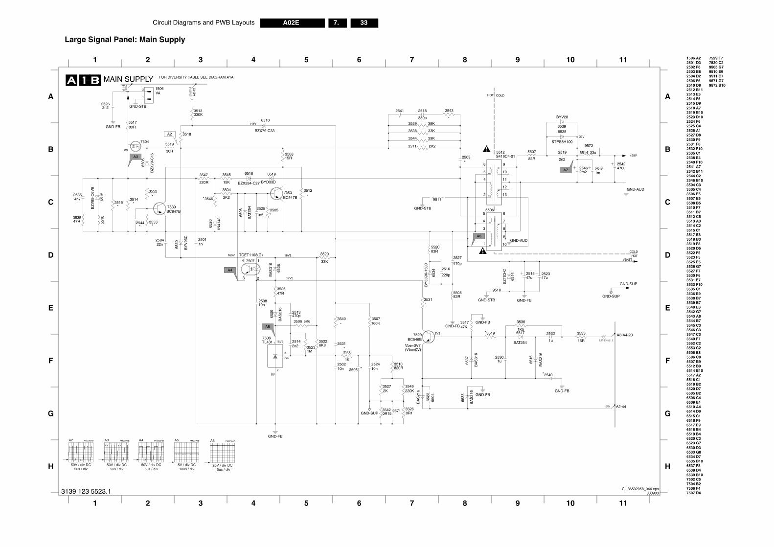
Circuit Diagrams and PWB Layouts 33A02E 7.
A
B
C
D
E
F
G
H
1506 A22501 D32502 F62503 B82504 D22506 F62510 D82512 B112513 E52514 F52515 D92518 A72519 B102523 D102524 F62525 C4
10 11
10 11
2526 A12527 D82530 F92531 F62532 F102535 C12538 E42540 F102541 A72542 B112544 C22546 B103504 C33505 C43506 E53507 E63508 B53510 F73511 B73512 C53513 A33514 C23515 C13517 E83518 B33519 F83520 D53522 F53523 F53525 E53526 G73527 F73530 F63531 E73533 F103535 C13536 E93538 B73539 B73540 E63542 G73543 A83544 B73545 C33546 C33547 C33549 F73552 C23553 C25505 E85506 C85507 B95512 B95514 B105517 A25518 C15519 B2
3533
15R
5520 D76505 B26506 C46509 E46510 A46514 D96515 C16516 F96517 E96518 B46519 B46520 C36523 G76530 D36533 G86534 D76535 B106537 F86538 D46539 B107502 C57504 B27506 F47507 D4
7529 F77530 C29505 G79510 E99511 C79571 G79572 B10
GND-FB
252347u
07
R
BYV28
6539
9572
*
HOTCOLD
A2-44
A3-A4-23
32V
2519
2n2
A7
3527
5
GND-SUP
3549
2542470u
1m2512
1u
2532
6516
BA
S21
6
33u5514
GND-AUD
2540
6535
STPS8H100
25462m2
+28V
VBATT
GND-SUP
CL 36532058_044.eps030903
G
H
1 2 3 4 5 6 7 8 9
GND-SUP
GND-FB
GND-FB
9571
2K
BA
S21
6
6523
6533
BA
S21
6220K
9505
35420R15 0R1
3526
A2
50V / div DC5us / div
PM3394B A3
50V / div DC5us / div
PM3394B A4
50V / div DC5us / div
PM3394B A5
5V / div DC10us / div
PM3394B A6
20V / div DC10us / div
PM3394B
3139 123 5523.1
Large Signal Panel: Main Supply
A3
E
F
1 2 3 4 5 6 7 8 9
A
B
C
D
30R
5519
A5
2541
353547R
3519
GND-FB
470p
470p
2527
1
2 1506VA
1K5
3536
3546
3505
22n2504
10n2524
820R3510
2K2
3504
2531
10n2502
6519
BYD33D
1u2530
3518
1M3523
BC847B7530
9
55
83
A2
330p
2518
2510
220p
GND-STB
GND-STB
BY
359X
-150
0
7507
TCET1103(G)
5512S419C4-01
10
11
12
132
4
5
6 9
GND-FB
7502BC547B
BZ
X79
-C15
6505
A6
A4
3515
BC546B7529
3543
10n2538
2513
47K3517
17V2
169V 18V2
*
*
144V
16V6
*
*
*
2V2
*
*
*
*
A2-
12A1-
8
*
*
COLDHOT
Vbe=0V7(Vbe=0V)
*
0V
*
MAIN SUPPLY
*
*
0V
*
2V5
*
3538 33K
3539 39K
5K63506
2n22526
3514
GND-FB
6515
BZ
V85
-C6V
8
2544
3552
2506
83R5505
47u251
3553
GND-STB
15R3508
GND-FB
33K
3520
BZX79-C33
6510
47R3525
BZX284-C27
6518
6537
BA
S31
6
14
3 2
BA
S31
6
6538
3531
3544 39K
BAT254
6517
83R5517
BY
V95
C
6530
2503
330K3513
83R5520
6534
7504
25142n2
9510
220R
3547
5518 B
AT25
4
160K350765
09
BA
S21
6
6506
1 10
3
4
5 6
7
8
1n5
2525 5506
2K23511
3540
6514
BZ
T03
-C
1K
3530
2
1
3
25354n7
6K83522
7506TL431
15K
3545
1n2501 GND-AUD
9511
3512
6520
1N41
48
FOR DIVERSITY TABLE SEE DIAGRAM A1A
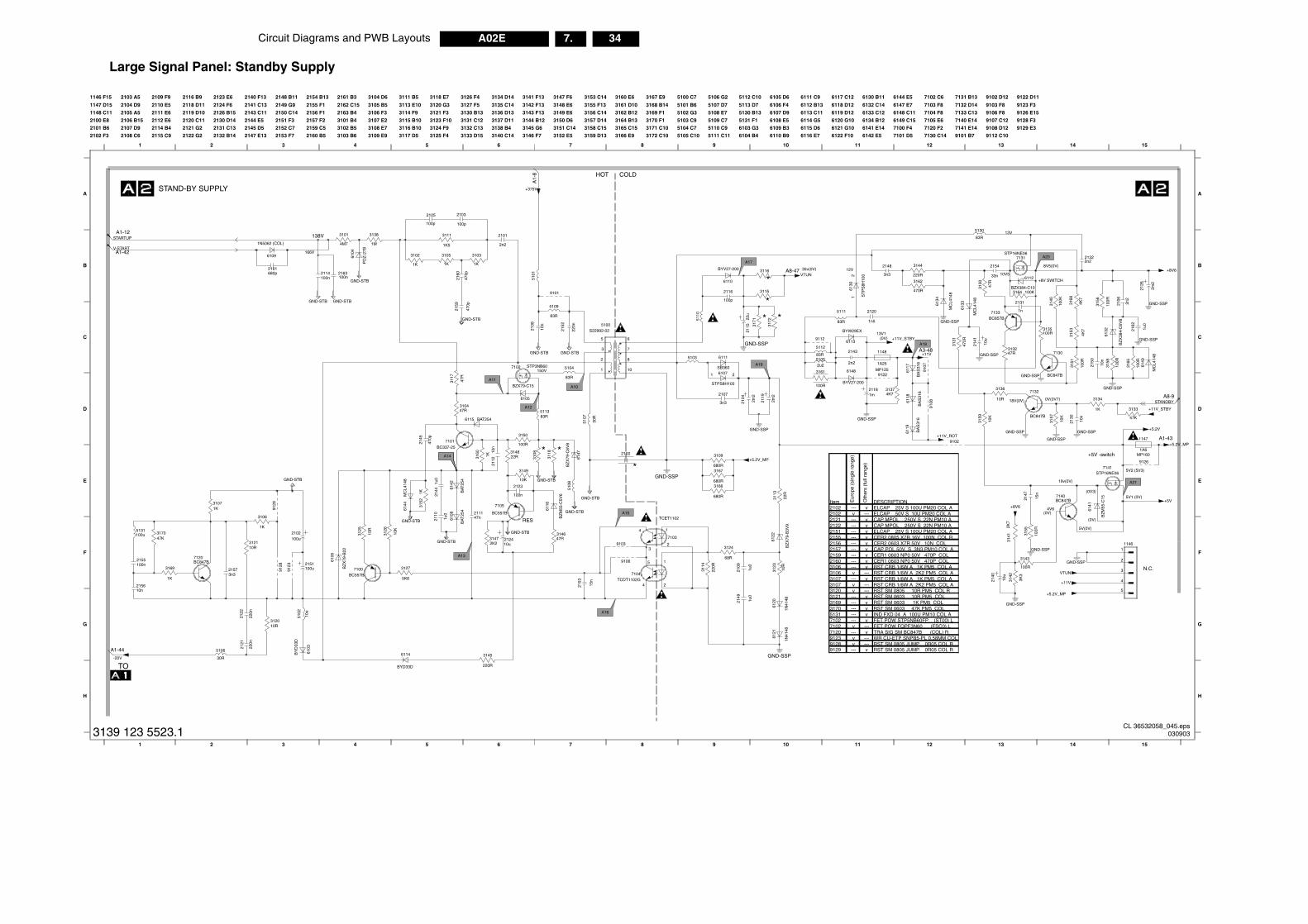
34A02E 7.Circuit Diagrams and PWB Layouts
(0V)
5V1 (0V)(0V3)
A
B
C
D
E
F
G
H
12 13 14 15
12 13 14 15
+5V -switch
5V2 (5V3)
N.C.
A3-48
A1-43
4V6
A1-44
(0V)
+8V SWITCH
44 E5
47 E7
48 C11
49 C15
00 F4
01 D5
7102 C6
7103 F8
7104 F8
7105 E6
7120 F2
7130 C14
7131 B13
7132 D14
7133 C13
7140 E14
7141 E14
9101 B7
9102 D12
9103 F8
9106 F8
A8-9
9107 C12
9108 D12
9112 C10
9122 D11
9123 F3
9126 E15
9128 F3
9129 E3
5V(0V)
10u
2141
9108
100R
2162
1u0
3158
100R
2154
33n
9126
GND-SSP
2150
10n
10K
3157
3168
4K7
6141
BZ
M55
-C15
3151
100R
313247R
3131
470R
GND-SSP
GND-SSP
GND-SSP
220R
3144
30R
5106
100R
3143
1A6MP160
1147
GND-SSP
3155
100R
STP16NE067141
7140BC847B
3162
470R
BC847B
7130
100R3135
3130
47R
7132
BC847B
9107
6119
BA
S31
6
6133
MC
L414
8
7133BC857B
3145
GND-SSP
A21
A20
3
4
5
11461
2
3K3
3142
3140
100K
BY
D
18V(0V) 0V(0V7)
19v(0V)
13V
10V5
8V5(0V)
610
2140
10u
GND-SSP
2 2
21322n2
GND-SSP
5130
83R
3164 100K
6112
BZX384-C10
6117
BA
S31
6B
AS
316
6118
9102
2K7
3141
6149
MC
L414
8
3159
10K
2m2
2126
6114
GND-SSP
GND-SSP
A18
GND-SSP
2147
15n
3153
4K7
1n
2131
6132
BZ
X38
4-C
6V8
GND-SSP
2106
2n2
3136
10R
6134
MC
L414
8
3165
100R
STP16NE067131
3156
3134
1K
GND-SSP
10n
2130 47K
3133
+11V_ROT
+8V6+5V
STANDBY
+11V_STBY
+8V6
+11V
V_STBY
+5.2V_MP
+11V
VTUN
-20V
+5.2V
+5.2V_MP
CL 36532058_045.eps030903
IONV S 100U PM20 COL AV S 10U PM20 COL A
250V S 22N PM10 A 250V S 22N PM10 AV S 100U PM20 COL A
X7R 16V 100N COL R X7R 50V 10N COL0V S 3N3 PM10 COL A NP0 50V 470P COL NP0 50V 470P COL/6W A 1K PM5 COL A/6W A 2K2 PM5 COL A/6W A 1K PM5 COL A/6W A 2K2 PM5 COL A05 10R PM5 COL R03 10R PM5 COL03 1K PM5 COL03 47K PM5 COL A 100U PM10 COL ATP5NB60FP (ST00) LQPF3N60 (FSC0) L BC847B (COL) R SNPB5-PL 0.58MM COL
05 JUMP. 0R05 COL R9129 --- v RST SM 0805 JUMP. 0R05 COL R
H
1 2 3 4 5 6 7 8 9 10 11
TO 220RBYD33D
3139 123 5523.1
Large Signal Panel: Standby Supply
(0V)
A
B
C
D
E
F
G
1146 F15
1147 D15
1148 C11
2100 E8
2101 B6
2102 F3
2103 A5
2104 D9
2105 A5
2106 B15
2107 D9
2108 C6
1 2 3 4 5 6 7 8 9 10 11
*
*
* *
2109 F9
2110 E5
2111 E6
2112 E6
2114 B4
2115 C9
2116 B9
2118 D11
2119 D10
2120 C11
2121 G2
2122 G2
2123 E6
2124 F6
2126 B15
2130 D14
2131 C13
2132 B14
2140 F13
2141 C13
2143 C11
2144 E5
2145 D5
2147 E13
2148 B11
2149 G9
2150 C14
2151 F3
2152 C7
2153 F7
2154 B13
2155 F1
2156 F1
2157 F2
2159 C5
2160 B5
2161 B3
2162 C15
2163 B4
3101 B4
3102 B5
3103 B6
3104 D6
3105 B5
3106 F3
3107 E2
3108 E7
3109 E9
3111 B5
3113 E10
35v(0V)
3114 F9
3115 B10
3116 B10
3117 D5
3118 E7
3120 G3
3121 F3
3123 F10
3124 F9
3125 F4
3126 F4
3127 F5
3130 B13
3131 C12
3132 C13
3133 D15
3134 D14
3135 C14
3136 D13
3137 D11
3138 B4
A8-47
138V
A1-
8 HOT
STAND-BY SUPPLY
3140 C14
3141 F13
3142 F13
3143 F13
3144 B12
3145 G6
3146 F7
3147 F6
3148 E6
3149 E6
3150 D6
3151 C14
3152 E5
3153 C14
3155 F13
3156 C14
3157 D14
3158 C15
3159 D13
3160 E6
3161 D10
3162 B12
3164 B13
3165 C15
3166 E9
A1-12
A1-42
RES
166V
3167 E9
3168 B14
3169 F1
3170 F1
3171 C10
3172 C10
5100 C7
5101 B6
5102 G3
5103 C9
5104 C7
5105 C10
5106 G2
5107 D7
5108 E7
5109 C7
5110 C9
5111 C11
5112 C10
5113 D7
5130 B13
5131 F1
6103 G3
6104 B4
150V
6105 D6
6106 F4
6107 D9
6108 E5
6109 B3
6110 B9
6111 C9
6112 B13
6113 C11
6114 G5
6115 D6
6116 E7
6117 C12
6118 D12
6119 D12
6120 G10
6121 G10
6122 F10
6130 B11
6132 C14
6133 C12
6134 B12
6141 E14
6142 E5
61
61
61
13V1
61
71
71
* *
*
COLD
2148
3n3
5101
6104
PD
Z-2
7B
91062151100u
A13
A16
GND-STB
GND-STB
51052u2
3115
9122
2124
MP125
1148
1A25
1K
3169
GND-STB
12
1n5
2120
A19
2153
6148
BYV27-200
A12
A11
6147
BZ
X79
-C6V
8
2143
2n2
GND-STB
10u
5100
1N5062 (COL)
6109
10R3121
22R
3113
2100
3106
1K
GND-SSP
1 2
1K
3103
3118
1K
3105
9101
5109
83R
A14
A15
100nGND-STB
2114
100p
2103
10R3120
100p
2105
29103
STPS8H100
6107
GND-STB
GND-STB
6115 BAT254
BZ
M55
-C5V
6
100R
3150
30R
5107
83R
5112
2108
10n
5108
GND-STB
3116
15R
3125
3127
5K6
6121
1N41
48
33D
15
4 2
12V
1N41
48
6120
BC337-25
7101
6110
BYV27-200
7104TCDT1102G
BYW29EX
1m2118
4M7
3101
GND-STB
6113
220R
3114
7102 STP3NB60
6108
BAT
254
BZ
X79
-B22
6106
310
u
5102
3n3
2107
BZ
X79
-B3V
9
6122
220n
2122
3108
121
20n
2n2
1K
3102
BZX79-C15
6105
GND-STB
2101
47R
3117
470p
2160
TCET1102
7103
14
3
470p
2159
3111
1K5
GND-STB
A10
47R3104
10K
3126
5103 6111
SB360
1u0
2109
47n2111
10R
3123
68R
3124
2102100u
1K3107
31374K7
3166
680R
3167
680R
S22992-02
1 10
2
3
5 6
7
8
BAT
254
61421u
021
4421
10
BC557B7100
1u0
100n
2123
BC557B
7105
5104
83R
10K
3149
15n
220n
2152
A17
6116
47R3146
2K23147
MC
L414
861
44
2145
470p
ST
PS
8H10
0
6130
511383R
3161
100R
2149
1u0
3160
1K
3152
1K
5110
9112
10n
2112
22R3148
47K3170100u
5131
2155100n
GND-STB
GND-STB
GND-SSP
2163100n
100p
2116
83R
5111
3172
3171
GND-SSP
3n32157 91
23
9129
10n2156
BC847B7120
9128
3138
1M
2161680p
GND-SSP
22u
2115
2104
2m2
680R
3109
2m2
2119
+375V
V-START
VTUN
+11
+5.2V_MP
STARTUP
Item Eur
ope
(sin
gle
rang
e)
Oth
ers
(ful
l ran
ge)
DESCRIPT2102 --- v ELCAP 252102 v --- ELCAP 502121 --- v CAP MPOL2122 --- v CAP MPOL2151 --- v ELCAP 252155 --- v CER2 08052156 --- v CER2 06032157 --- v CAP POL 52159 --- v CER1 06032160 --- v CER1 06033106 --- v RST CRB 13106 v --- RST CRB 13107 --- v RST CRB 13107 v --- RST CRB 13120 v --- RST SM 083121 --- v RST SM 063169 --- v RST SM 063170 --- v RST SM 065131 --- v IND FXD 047102 --- v FET POW S7102 v --- FET POW F7120 --- v TRA SIG SM9123 v --- WR CU-ETP9128 v --- RST SM 08
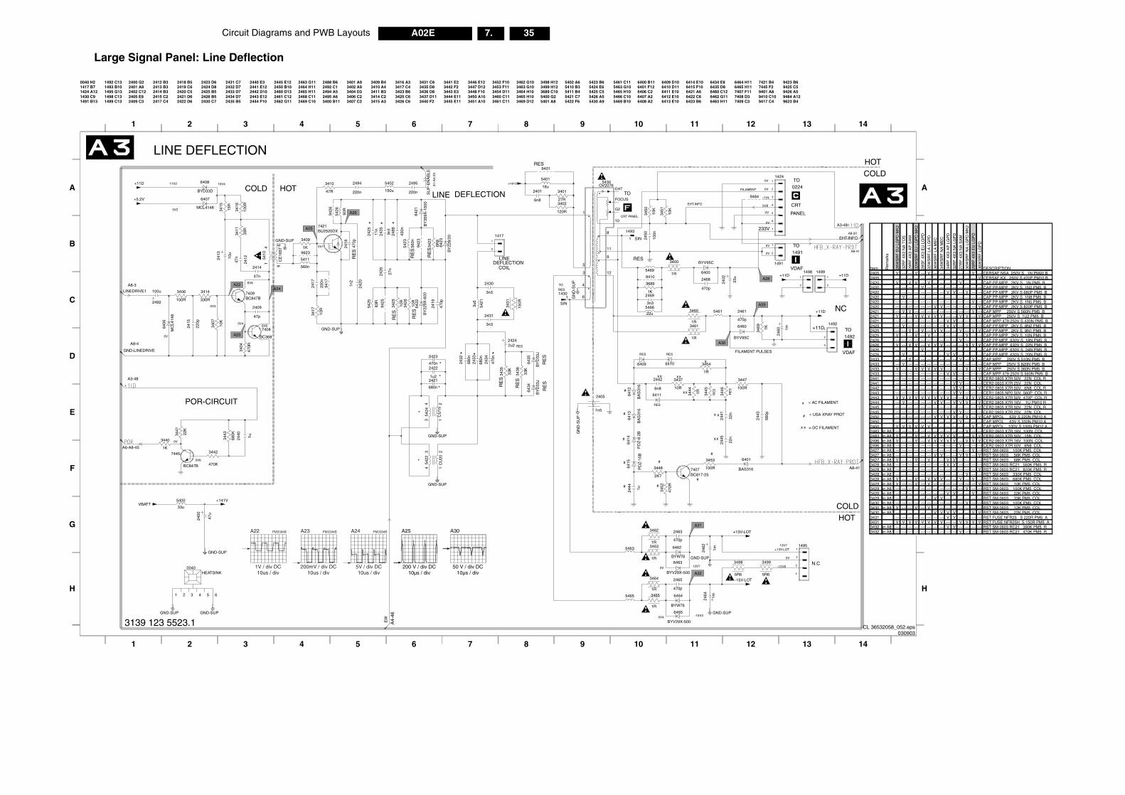
Circuit Diagrams and PWB Layouts 35A02E 7.
CRT
x
A
B
C
D
E
F
G
H
NC
13 14
A8-41
A8-41
TO
+11D
13 14
0V
-12V8
TO
VDAF
HOT
13V7
COLD
0
9423 B69425 C59426 A59484 A129623 B4
1492
VDAF
COLDHOT
A8-20
TO
#
x
PANEL
= USA XRAY PROT
N.C
= AC FILAMENT
1491
+13V-LOT
x = DC FILAMENT
A3-48
0224
13V7
1
2
1491
14951
1424
64631R
14991
2
GND-SUP 2
3
4
14921
2
3
1m
2460
1498
3498 3499
+11D+11D
+11D
EHT-INFO
CL 36532058_052.eps030903
Item Rem
arks
28W
SR
F E
U L
GP
D M
K2
32R
F 4
X3
NA
TO
S
29R
F 4
X3
AP
SA
M
32W
SR
F E
U L
GP
D M
K2
28S
F 4
X3
EU
LG
PD
32W
SR
F L
A L
GP
D
36W
SR
F L
A M
EC
34W
SR
F N
A M
EC
34R
F 4
X3
AP
LG
PD
32R
F 4
X3
NA
LG
PD
27R
F 4
X3
NA
SA
M
30W
SR
F N
A L
GP
D M
K2
29R
F 4
X3
EU
LG
PD
36W
SR
F L
GP
D
DESCRIPTION2405 V --- --- V --- V --- --- --- --- --- --- V --- CERSAF NSA 250V S 1N PM20 B2405 --- --- --- --- --- --- --- --- --- --- --- --- --- V CERSAF KX 250V S 470P PM10 B2420 V --- V V --- V --- --- --- --- V --- --- --- CAP PP-MPP 2KV S 1N PM5 B2420 --- --- --- --- V --- --- --- --- --- --- --- --- --- CAP PP-MPP 2KV S 1N2 PM5 B2420 --- --- --- --- --- --- --- --- V V --- V --- --- CAP PP-MPP 2KV S 680P PM5 B2420 --- V --- --- --- --- --- --- --- --- --- --- --- --- CAP PP-MPP 2KV S 1N8 PM5 B2420 --- --- --- --- --- --- --- --- --- --- --- --- V --- CAP PP-MPP 2KV S 1N5 PM5 B2420 --- --- --- --- --- --- V V --- --- --- --- --- V CAP PP-MPP 2KV S 820P PM5 B2421 --- V V --- --- --- --- --- --- --- --- --- V --- CAP MPP 250V S 560N PM5 B2421 V --- --- V V V V V --- --- V V --- V CAP MPP 250V S 1U2 PM5 B2421 --- --- --- --- --- --- --- --- V V --- --- --- --- CAP MPP 479 250V S 430N PM5 B2425 --- V --- --- --- --- --- --- V V --- --- --- --- CAP PP-MPP 2KV S 8N2 PM5 B2425 --- --- V --- V --- V V --- --- V --- V V CAP PP-MPP 2KV S 9N1 PM5 B2425 V --- --- V --- V --- --- --- --- --- V --- --- CAP PP-MPP 2KV S 10N PM5 B2426 --- --- --- --- --- --- --- --- --- --- V --- --- --- CAP PP-MPP 630V S 18N PM5 B2426 V --- V V --- V V V --- --- --- V V V CAP PP-MPP 630V S 22N PM5 B2426 --- --- --- --- V --- --- --- --- --- --- --- --- --- CAP PP-MPP 630V S 24N PM5 B2426 --- V --- --- --- --- --- --- V V --- --- --- --- CAP PP-MPP 630V S 20N PM5 B2433 --- --- V --- --- --- --- --- --- --- V --- V --- CAP MPP 250V S 510N PM5 B2433 --- V --- --- --- --- --- --- --- --- --- --- --- --- CAP MPP 250V S 820N PM5 B2433 V --- --- V V V V V --- --- --- V --- V CAP MPP 250V S 360N PM5 B2433 --- --- --- --- --- --- --- --- V V --- --- --- --- CAP MPP 479 250V S 560N PM5 B2441 --- --- --- --- --- --- --- --- --- --- --- --- --- V CER2 0805 X7R 50V 22N COL R2441 --- --- --- --- --- --- --- --- --- V V --- --- --- CER2 0603 X7R 25V 22N COL2442 --- --- --- --- --- --- --- --- --- V V --- --- V CER2 0805 X7R 50V 6N8 COL R2443 --- --- --- --- --- --- --- --- --- V V --- --- --- CER1 0805 NP0 50V 560P COL R2443 V V V V V V V V V --- --- V V V CER2 0805 X7R 50V 470P COL R2444 --- V --- --- --- --- V V --- V V V --- V CER2 0805 X7R 16V 1U PM10 R2445 --- --- --- --- --- --- --- --- --- --- --- --- --- V CER2 0805 X7R 50V 22N COL R2445 --- --- --- --- --- --- --- --- --- V V --- --- --- CER2 0603 X7R 25V 22N COL2450 --- --- --- --- --- --- V V V V --- V --- V CAP MPOL 63V S 220N PM10 A2450 --- --- --- --- --- --- --- --- --- --- V --- --- --- CAP MPOL 63V S 330N PM10 A2450 V V V V V V --- --- --- --- --- --- V --- CAP MPOL 100V S 100N PM10 A2483 in A8 --- --- --- --- --- --- --- --- --- --- --- V --- --- CER2 0603 X7R 16V 100N COL2483 in A8 V --- --- V --- V V V V V --- --- V V CER2 0603 X7R 50V 15N COL2496 in A8 V --- --- V --- V V V V V --- V V V CER2 0603 X7R 16V 100N COL2496 in A8 --- --- --- --- --- --- --- --- --- --- V --- --- --- CER2 0603 X7R 50V 6N8 COL3427 in A8 --- --- --- --- --- --- --- --- --- --- --- --- V --- RST SM 0603 100K PM5 COL3427 in A8 --- --- --- --- --- --- V V --- --- V V --- V RST SM 0603 56K PM5 COL3427 in A8 V --- --- V --- V --- --- V V --- --- --- --- RST SM 0603 68K PM5 COL3428 in A8 --- --- --- --- --- --- --- --- V V --- --- --- --- RST SM 0603 RC21 560K PM5 R3428 in A8 --- --- --- --- --- --- --- --- --- --- --- --- --- V RST SM 0603 RC21 820K PM5 R3428 in A8 --- --- --- --- --- --- --- --- --- --- --- V --- --- RST SM 0603 330K PM5 COL3428 in A8 V --- --- V --- V V V --- --- V --- V --- RST SM 0603 680K PM5 COL3429 in A8 V --- --- V --- V --- --- --- --- --- --- --- V RST SM 0603 10K PM5 COL3429 in A8 --- --- --- --- --- --- --- --- --- --- --- V --- --- RST SM 0603 100K PM5 COL3429 in A8 --- --- --- --- --- --- --- --- V V --- --- V --- RST SM 0603 22K PM5 COL3429 in A8 --- --- --- --- --- --- V V --- --- --- --- --- --- RST SM 0603 33K PM5 COL3430 in A8 --- --- --- --- --- --- --- --- --- --- --- V --- --- RST SM 0603 100K PM5 COL3430 in A8 V --- --- V --- V --- --- --- --- --- --- --- --- RST SM 0603 12K PM5 COL3430 in A8 --- --- --- --- --- --- V V V V --- --- V V RST SM 0603 22K PM5 COL3431 --- --- --- --- --- --- --- --- V V --- --- --- --- RST FUSE NFR25 S 220R PM5 A3431 V V V V V V V V --- --- V V V V RST FUSE NFR25H S 150R PM5 A3432 in A8 --- --- --- --- --- --- --- --- V V --- --- --- --- RST SM 0603 RC21 390K PM5 R3432 in A8 --- --- --- --- --- --- --- --- --- --- V --- --- --- RST SM 0603 RC21 470K PM5 R
H
-15V2
0V
1 2 3 4 5 6 7 8 9 10 11 12
A4-
46 0V4
6464
BYW76
BYV29X-500
64651R
3465
3464
1R
A32
2465
470p
2464
1m
GND-SUP
BYV29X-500
GND-SUPGND-SUP
1 2 3 4 5 6
5R6
0040HEATSINK 5R6
5465
EW
-15V-LOT
3139 123 5523.1
200 V / div DC10µs / div
50 V / div DC10µs / div
1V / div DC10us / div
200mV / div DC10us / div
5V / div DC10us / div
Large Signal Panel: Line Deflection
FOCUS
EHT
G2
*
RE
S
*
#
*
xx
G
0040 H21417 B71424 A121430 C91491 B13
1492 C131493 B101495 G131498 C131499 C13
2400 G22401 A8
0V4
6V6
x
0V
10V4
#
RE
S
FILAMENT PULSES
#
1 2 3 4 5 6 7 8 9 10 11 12
RES
RES
RES
LINE
**
RES
A
B
C
D
E
F
A3-48
*
FILAMENT
A8-3
*
RE
S
RES
COIL
RES
2402 C122405 E92409 C3
2412 B32413 B32414 B32415 C22417 C4
2418 B52419 C62420 C52421 D62422 D6
2423 D62424 D82425 B52426 B52430 C7
0V
x
2431 C72432 D72433 D72434 D72435 B5
2440 E32441 E122442 D102443 E122444 F10
2445 E122450 B102460 D132461 C122462 G11
2463 G112464 H112465 H112468 C112469 C10
2488 B62492 C12494 A52495 A63400 B11
3401 A93402 A93404 D33406 C23407 C2
3409 B43410 A43411 B33414 C23415 A3
3416 A33417 C43423 B63425 C63426 C6
3431 C83435 D83436 D83437 D113440 F2
3441 E23442 F23443 E33444 E113445 E11
3446 E123447 D123448 F103450 A103451 A10
3452 F103453 F113454 D113460 C113461 C11
3462 G103463 G103464 H103465 H103469 D12
3498 H123499 H123689 C105400 G25401 A8
5402 A65410 B35411 B45421 C75422 F6
5423 B65424 E65425 C55426 A55430 A9
5461 C115463 G105465 H105466 C105469 B10
6400 B116401 F126406 C26407 A26408 A2
6409 D106410 D116411 E106412 E106413 E10
6414 E106415 F106421 A66422 C66423 B6
6434 E86435 D86460 C126462 G116463 H11
6464 H116465 H117407 F117408 D37409 C3
7421 B47445 F29401 A89410 C19417 C4
0V
11V2
0V6
RE
S
233V
*
0V1
*
0V
TO
x
#
RE
S
RE
S
RE
S
RES
HOT-1V4
RE
S
x
0V
0V
*
TO
5V2
#
x
COLD
CRT PANEL
x
#
#
x
#
*
LINE DEFLECTION
DEFLECTION
DEFLECTION
POR-CIRCUIT
A8-4
A1-
A4-
23
x
5V8
#
A6-A8-45
RE
S
LINE
EHT-INFO
6V60V4
RE
S
x
0V
RE
S
0V
3446
2423
470n
2431
3n3
A29
6460
BYV95C
A28
6423
BY
228/
20
560n
5423
2430
680n
2432
100R
3406
1u2444
7408
BC368
1
2
10R
3426
3452
470R
A22
5469
1K
3409
7407BC817-25
A25
470p
2463
100u
2492
GND-SUP
GN
D-S
UP
18u
5401
3442
2443
560p
33K
3435
10K
3451
330R
3414
3437
10R
10K
3407
6414
6415
PD
Z-1
5B
220n
2417
5400
33u
22n
2445
2488
430n
1K
3689
5425
83R
PD
Z-8
.2B
9426
470p
6n8
2442
3402
120R
2421
680n
A30
3447
100R
SIN
14301
GND-SUP
GND-SUP
3u6
5421
4
CU
20
5422
12
4
96
47R
3410
220n
2494
CU
15
5424
43
21
BC847B7409
BYW76
6462
6434
3n3
5463
3441
22K
GND-SUP
8
9
1n2
2420
5430OV2076
1
10
11
123
4
5
6
47n
2414
1
2
3
4
5
6
7
GN
D-S
UP
6421
BY
359X
-150
0
3436
33K
22n
2441
3448
2K7
470p
2461
1R
3454
1n5
2405
BA
S31
6
6413
2412
47n
2469
3n3
22u
5466
2400
100R
3416
6435
BY
D33
J
47u
6411
7445
BC847B
220p
2415
150R
3431
BYV95C
6400
6408
BYD33D
9410
680K
3443
BY
D33
J
470p
2418
2426
27n
1m2462
3453
100R
11n
2425
MCL4148
6407
6422
BY
229X
-600
1u2
2422
2495
220n
5461
3463
10R
3425
A23
47p
2409
9417
470R
3404
3450
10K
470p
2419
9425
2468
2u22424
15R
3415
100n
2450
1R
3460
3461
1R
9423
680n
2433
470K
470n
2434
14171
2
1R
3462
3469 1K
3445
BA
S31
6
6412
A31
10u
2413
560n
5411
BAS316
6401
3400
150u
5402
1R
90R
5426
9623
10R
3417
1K
3440
A26
39R
3411
2440 1u
A24
9n1
2435
6R8
3423
3401
27R
33u
2402
MC
L414
8
6406
2401
6n8
9401
GND-SUP
6410
3
6409
3444
1R
CE
165T
5410
1
1
7421BU2520DX
SIN
1493
9484
+141V
+13V-LOT
SU
P-E
NA
BLE
+11D
LINEDRIVE1
VBATT+141V
+5.2V
GND-LINEDRIVE
A25 A30A22 PM3394B A23 PM3394B A24 PM3394B

36A02E 7.Circuit Diagrams and PWB Layouts
RES
FRAME
DEFLECTION
COIL
ON CIRCUIT
(SEE NOTE)
A1-A3-23
A3-
46
-16V
0V7
H
A
B
C
D
E
F
G
H
13
13
458
-C5V
6
2
9405 G39481 G49482 G79483 F79499 G12
B
9620 C109622 C10
3497
16271
2
3
GND-SUP
33K
GND-SUP
GND-SUP
3495
33K
470n
2498
3n3
2499
6499
BZ
X38
4-C
10
6491
1PS76SB10
16251
2
3
3403
100R
-SUP
SUP-ENABLE
CL 36532058_046.eps040903
Item 28/3
2" W
SR
F L
GP
D
34/3
6" 4
:3 R
F T
OS
J
29"
4:3
RF
SM
GK
28"
4:3
SF
PH
CO
36"
WS
RF
ME
C
32R
F 4
X3
NA
LG
PD
27R
F 4
X3
NA
SA
M
30W
SR
F N
A L
GP
D
34 4
:3R
F A
P L
GP
D
32W
SR
F L
GP
D M
KII
29R
F E
U L
GP
D
36W
SR
F_L
GP
D
DESCRIPTION1625 V V V V --- V V V V V V --- CON V 3P M 2.50 BK EH-A B1627 --- --- --- --- V --- --- --- --- --- --- V CON V 3P M 2.50 BK EH-A B2490 V V V V --- --- --- --- --- V V --- ELCAP 10V S 100U PM20 COL A2490 --- --- --- --- V V V V V --- --- V ELCAP 50V S 100U PM20 COL A2498 V V V V --- --- --- --- --- V V --- CER2 0805 X7R 16V 1U PM10 R2633 V V V V --- V V V V V V --- CER2 0603 X7R 50V 3N3 COL2633 --- --- --- --- V --- --- --- --- --- --- V CER2 0603 X7R 50V 6N8 COL2653 --- --- V --- --- --- --- --- --- --- V --- CER2 0603 X7R 50V 2N7 PM10 R2653 --- --- --- --- V V V V V --- --- V CER2 0603 X7R 50V 2N2 COL2653 V V --- V --- --- --- --- --- V --- --- CER2 0603 X7R 50V 3N3 COL2661 --- --- --- --- V --- --- --- --- --- --- V CER2 0603 X7R 50V 6N8 COL2662 --- --- --- --- V V V V V --- --- V CER2 0603 X7R 50V 3N3 COL3403 V V V V V V V V V V V V RST CRB 1/6W A 100R PM5 COL A3412 V V V V V V V V V V V V RST SM 0603 1K2 PM5 COL3418 --- --- --- --- V --- --- --- --- --- --- V RST MFLM MBB0207 A 47K PM1 A3418 V V V V --- V V V V V V --- RST MFLM MBB0207 A 56K PM1 A3480 V --- --- V V --- --- V --- V --- V RST FUSE NFR25 S 4R7 PM5 A3480 --- V V --- --- V V --- V --- V --- RST FUSE NFR25 S 6R8 PM5 A3483 V --- V V V --- V V --- V V V RST SM 0603 1K8 PM5 COL3483 --- V --- --- --- V --- --- V --- --- --- RST SM 0603 2K2 PM5 COL3484 --- --- --- --- V V V V V --- --- V RST SM 0603 4K7 PM5 COL3488 V --- V V V --- V V --- V V V RST MFLM MBB0207 A 1M PM1 A3491 --- --- --- --- --- V V V V --- --- --- RST SM 0603 27K PM5 COL3491 --- --- --- --- V --- --- --- --- --- --- V RST SM 0603 39K PM5 COL3491 V V V V --- --- --- --- --- V V --- RST SM 0603 47K PM5 COL3493 V V V V --- --- --- --- --- V V --- RST MFLM MBB0207 A 150K PM1 A3495 V V V V --- --- --- --- --- V V --- RST MFLM MBB0207 A 15K PM1 A3620 V --- --- --- --- --- --- --- --- V --- --- RST CRB CFR25S A 1R8 PM5 A3620 --- --- --- V V --- --- --- --- --- --- V RST CRB CFR25S A 1R5 PM5 A3620 --- V --- --- --- --- --- V --- --- --- --- RST CRB CFR25S A 1R2 PM5 A3620 --- --- V --- --- V V --- V --- V --- RST CRB 1/6W A 1R PM5 COL A3621 --- --- --- --- V --- --- V --- --- --- V RST CRB CFR25S A 1R5 PM5 A3621 --- V --- --- --- --- --- --- V --- --- --- RST CRB CFR25S A 1R2 PM5 A3621 V --- V V --- V V --- --- V V --- RST CRB 1/6W A 1R PM5 COL A3622 V --- --- --- --- --- --- --- --- --- --- --- RST CRB ERDS2T A 3R3 PM5 A3622 --- --- --- V V --- --- V --- --- --- V RST CRB CFR25S A 1R5 PM5 A3622 --- V V --- --- --- --- --- --- --- --- --- RST CRB CFR25S A 1R2 PM5 A3622 --- --- --- --- --- --- V --- --- --- --- --- RST CRB 1/6W A 1R PM5 COL A3622 --- --- --- --- --- V --- --- V V --- --- RST CRB 1/6W A 2R2 PM5 COL A3623 V V V V V V --- V V V V V RST CRB 1/6W A 18K PM5 COL A3623 --- --- --- --- --- --- V --- --- --- --- --- RST CRB 1/6W A 22K PM5 COL A3625 --- --- V --- --- V V --- V --- V --- RST CRB 1/6W A 120R PM5 COL A3625 --- --- --- --- V --- --- V --- --- --- V RST CRB 1/6W A 220R PM5 COL A3625 V V --- V --- --- --- --- --- V --- --- RST CRB 1/6W A 330R PM5 COL A3626 --- --- V --- --- V V --- V --- V --- RST CRB 1/6W A 100R PM5 COL A3626 --- --- --- --- V --- --- V --- --- --- V RST CRB 1/6W A 220R PM5 COL A3626 V V --- V --- --- --- --- --- V --- --- RST CRB 1/6W A 330R PM5 COL A3627 --- --- --- --- V V V V V --- --- V RST SM 0805 10K PM5 COL R3627 V V V V --- --- --- --- --- V V --- RST SM 0805 22K PM5 COL R3630 --- --- --- --- --- V --- --- V --- --- --- RST SM 0603 27K PM5 COL3630 V V V V V --- V V --- V V V RST SM 0603 33K PM5 COL3632 --- --- --- --- V --- --- --- --- --- --- V RST SM 0603 18K PM5 COL3632 --- --- --- --- --- V --- --- V --- --- --- RST SM 0603 33K PM5 COL3632 V V V V --- --- V V --- V V --- RST SM 0603 39K PM5 COL
NOTE BRIDGECOIL PROTECTION (5422) IS TRIGGERED VIA EW
A3-
46
(SEE DIAGRAM A3 ALSO)
1 2 3 4 5 6 7 8 9 10 11 12
6
BZ
X38
4
GND-SUPGND-SUPGND-SUPGND-SUPGND-SUP GND-SUP GND-SUP
EW EW
3139 123 5523.1
A40
2 V / div AC5ms / div
A41
2 V / div AC5ms / div
A42
10 V / div AC5ms / div
A43
10V / div DC2ms / div
PM3394B A44
200mV / div DC2ms / div
PM3394B A45
1V / div DC10µs / div
PM3394B A47
50V / div DC10µs / div
PM3394BA46
500mV / div DC10µs / div
PM3394B A48
500mV / div DC10µs / div
PM3394B
Large Signal Panel: Frame Deflection & E/W Drive
FLYBACKGENERATOR
POWERAMPLIFIER
THERMALPROTECTION
FRAMEEW
COLD HOT
RE
S
RE
S
FRAME DEFLECTION & E/W DRIVE
FRAME DEFLECTION
-
GD
S
* * *
RE
SRES
RE
SR
ES
RE
S
PROTECTI
13V7
-3V6
-15V2
4V1
0V1
-0V9
8V2
1V9
21V2
-11V7
21V2
0V321V1
22V5
22V7
1V
5V7
0V4
7V8
0V61V2
0V
0V7
7V9
0V
0V
0V5
0V
1V3
0V
0V4
7V9
2V6
7V9A8-10
A8-11
A8-41
A8-6
TO
VDAF
RES
RE
S
RES
RE
S
RES RES
RE
S
RE
S
1V1
1V1
1V3
1V2
1V5
1V5
2V4
1V6
1V2
3V5
3V
13V5
12V3
0V
0V9
0V3
-10V
0V
21V1
3661
150R
G
1625 D121627 D121693 G42403 E32404 E22448 C112451 H22454 G2
2457 F32458 F12466 E122480 G92481 G82482 H92487 B122490 F7
8Vb
FRAMEDRIVE+
8Vb
FRAMEDRIVE-
8Vb
EW-DRIVE
1 2 3 4 5 6 7 8 9 10 11 12
A
B
C
D
E
F
2491 G122493 H32497 F112498 G132499 F122603 D62604 D92605 D5
2620 D92621 E92622 B102623 D32624 D102625 D10
2657
10n
2627 D112628 B7
2629 D122630 D82631 C82633 E62635 B82642 C112653 E102656 C2
2657 C32659 D12660 G112661 D7
3491
2662 D23403 B133412 F53418 G9
3419 E23420 E33421 E13422 E33449 G23455 E13456 E13457 E3
3458 F33459 F23466 F123467 B123472 F113474 F123475 G113476 F11
3478 G103479 G103480 G103481 G93482 G93483 G83484 G83485 G7
3486 G33487 G33488 F93489 G93490 F53491 G113492 F73493 F8
3495 G123496 H83497 E133610 C43611 D33620 E103621 E103622 E10
3623 E93624 D103625 D113626 D113627 D113628 B63629 D123630 C8
3631 C73632 D63633 C63634 D83635 B83636 B93637 B93638 C8
3639 D53640 B73641 D53642 C73643 C83644 C113645 B113646 D11
3647 D113648 E113652 C123653 D113654 G33655 C23656 C23657 D3
3658 D23659 D13660 C63661 D123662 C63663 D123664 D23665 C11
3688 H93690 D75467 G105620 C115621 C56405 B116442 C116455 F2
6456 G36457 H26458 H26480 F106481 G96482 G86483 G96491 F13
BAT254
6614
6493 G116494 G116499 G136614 D56615 F56616 D56617 C66618 C6
6619 D116620 B96621 B106622 C106623 C116624 D126625 A76626 A6
6627 A66628 D127440-A C37440-B E27441 E37442 E127443 B127450-A C4
7450-B G47455 F37480 G107482 G57483 F57486 G87487 G77611 C7
7612 E67613 B87614 D57620 C97641 B117652 C12
7442BC857B
7653 G17654 F12
BC8477443
MC
L414
8
6624
47K
3646
GND-SUP
4K7
3475
2R2
3647
6628
MC
L414
8
GND-SUP
10u
2487
3
2
BA
V99
6456
1
6627
MCL4148
2631
2u2
2603
220p
3648
1R
2491 10
u
3665
47R
3664
15K 6n8
26623690
1K
1n2661
6626
MCL4148
6625
MCL414864
57
BZ
X38
4-C
2V7
150K
3493
2605 1n
3422470K
3421
3K3
3420
3K3
2403
1n
1n
2404 3419
470K
1693
948194
05
3654
4K7
2493
3n3
150R
3663
3688
100K
3653
22K
BAT
254
6483
1K5
3662 330K
3643
6615
MC
L414
8
3K3
3490
A48
A46
A37
A38
A45 A47
A42
A43
A44
A49
A50
A39
A40
A41
A33
A35
A34
A36
2482
47n
15K
3489
26601n
680K
3488
2K2
3640
56K
3633
BC847B7611
6618
MCL4148
6617
MCL4148
5K6
3660
BC847B7614
470R
3641
6616
MC
L414
8
5621S13974
1 10
3
5 6
BA
S21
6
2458
560p
6482
56K
3639
2K2
3611
2K7
3496
100K
3467
GND-SUP
100n3466
4K7
2623
2n2
2466
3457
1K5
2659
22n
GND-SUP
22n
2656
3628
100u
2628
100u
GND-SUP
100R
100R
3492
2490
470p
2448
47K
3642
GND-SUP
47K
3449
1m2451
100R
GND-SUP
GND-SUP
GND-SUPGND-SUP
2633
3610
6K8
3n3
15n
2457
1K8
3412
3478
100R BAT254
6494
MC
L414
8
6493
2635
12
470R
3485
3635
330R
100n
3636
10K
3637
TL431CZ7613
2
1
3
22K
3476
3472
39K
2497
33n
220K
3474
56K
7654BC857B
9499
BY
D33
D
6480
7653BC847B
STP3NB607480
546756
K
3418
4R7
3480
100R
3479 4R
7
BZ
X28
4-C
15
6481
3481
100R
4n7
2480
2n2
2481
3482
3483
1K8
4K7
3484
BC847B7486
BC847B
7487
9483
9482
7483TCET1102
1 4
32
7482TCDT1102G
1 5
42
8K2
3487
15n
2454
6K8
3486
6K8
3456 7441
BC857B
1K2
3656
3K3
3455
12K
3655
2K2
3659
4
22K
36573658
22K
3634
LM393D7450-B5
6
7
8
39K 39K
BC847B7612
3632
33K
470K
3638
7450-ALM393D
3
2
1
8
4
3630
6455
MC
L414
8470R
3459
470R
3458
8
4
PMBT23697455
7
8
4
LM358N7440-A
3
2
1 2K2
7440-BLM358N
5
6
2u2
2630
3631
3622
3R3
GND-SUP
1R3620
3621
1R2653
3n3
GND-SUP
18K3623
2621
100n
2620
220n
2604 22
0n
150K
3645
GND-SUPGND
BZX79-C47
6405
BC847B
100u
2642 100R
3652
7652
GND-SUP
7641BC847B
MC
L414
8
6623
BZ
X28
4-C
1564
42
220R
3644
2629
100n
3625
120R
100R
3629
3627
3626
100R
10u
2627
22K
90R
6619
BY
D33
D
1R5
3624
5620
470n 470n
2624
9622
2625
100u
6622
BZ
V85
-C
6621
BYD33D2622
9620
6620
BYV27-200
7620
FLYB3
GND
4
IN+7
IN-1
OUT 5
VSUP
2 6
VSUPO
TDA8177
HFB_X-RAY-PROT
+141V
8Vb
+8V
-S
+141V
+8V-S
+13V-LOT
+8V-S
+11D 8Vb
8Vb
+13
V-L
OT
-15V-LOT
+141V
A33
500mV / div DC2ms / div
PM3394B
A34
500mV / div DC2ms / div
PM3394B
A35
500mV / div DC2ms / div
PM3394B
A36
200mV / div DC10us / div
PM3394B
A37
500mV / div DC2ms / div
PM3394B
A38
200mV / div DC10us / div
PM3394B
A39
2V / div DC10us / div
PM3394B
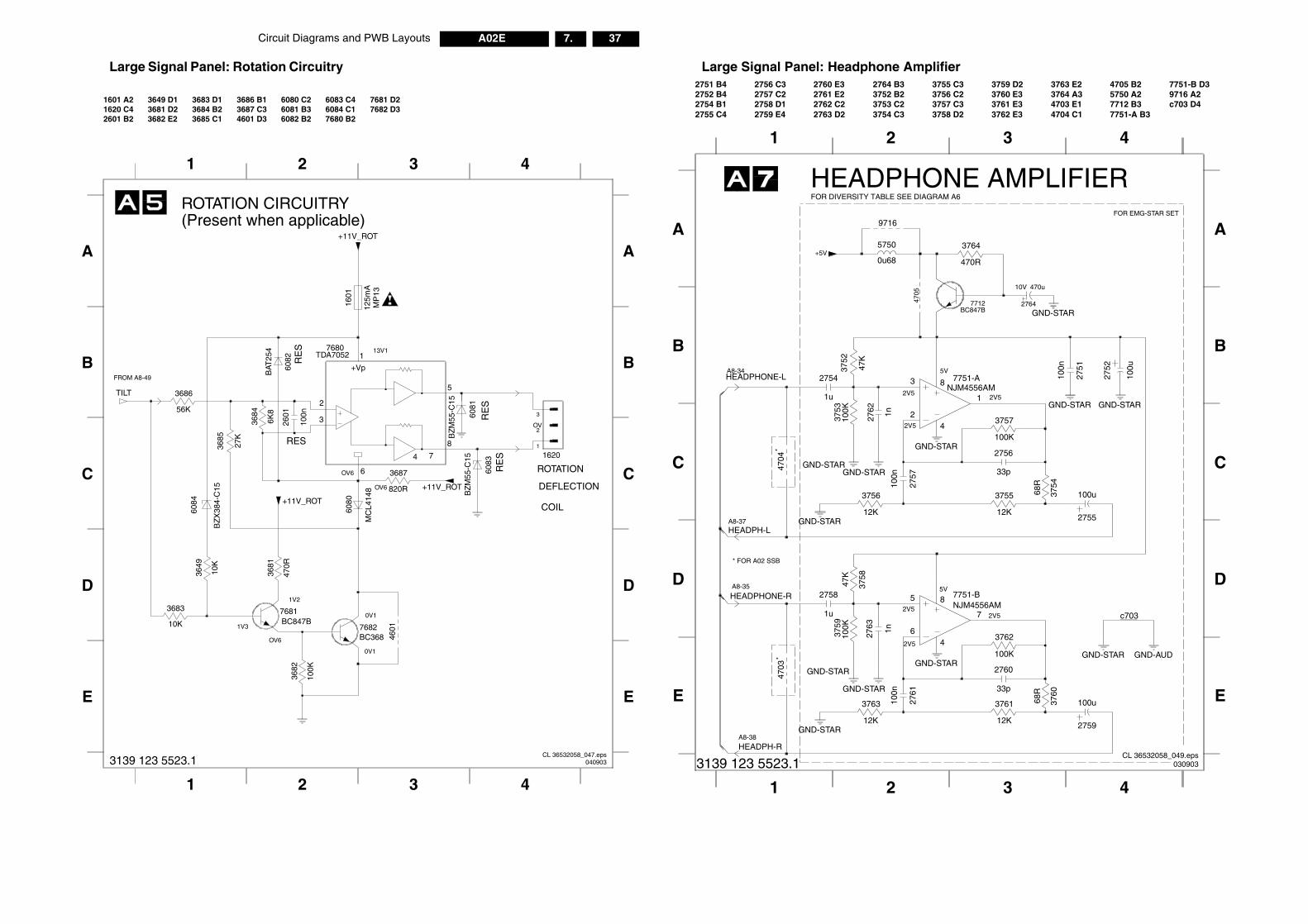
Circuit Diagrams and PWB Layouts 37A02E 7.
0V1
Amplifier
CL 36532058_049.eps030903
HONE AMPLIFIER
3 4
3 4
A
B
C
D
E
3223
3755 C33756 C23757 C33758 D2
3759 D23760 E33761 E33762 E3
3763 E23764 A34703 E14704 C1
4705 B25750 A2
2V5
FOR EMG-STAR SET
5V
7712 B37751-A B3
7751-B D39716 A2c703 D4
2V52V5
5V
2V5
2V52V5
GND-STAR
5
6
7
8
4
68R
3760
3754
68R
33p
2760
GND-STAR
12K
3761
GND-STAR
3755
12K
2761
GND-STAR
c703
GND-STAR2756
33p
100u
2755
2752
100u
3762
100K
4705
GND-STAR
4
2751
100n
7751-ANJM4556AM
3
2
1
8
2757
2759
100u
2764
470u10V
7751-BNJM4556AM
GND-AUD
100K
3757
7712BC847B
470R
3764
EE DIAGRAM A6
1 2 3 4
E E
100K
3682
CL 36532058_047.eps0409033139 123 5523.1
1 2
E
A8-38
*
GND-STAR4703
GND-STAR
100n
3763
12K
GND-STAR
HEADPH-R
3139 123 5523.1
Large Signal Panel: Rotation Circuitry
ROTATION CIRCUITRY
ROTATION
DEFLECTION
COIL
RE
S
RE
S
RE
S
RES
13V1
OV6
OV6
OV
1V2
OV6
0V1
1V3
FROM A8-49
1 2 3 4
A
B
C
D
A
B
C
D
1601 A21620 C42601 B2
3649 D13681 D23682 E2
3683 D13684 B23685 C1
3686 B13687 C34601 D3
6080 C26081 B36082 B2
6083 C46084 C17680 B2
7681 D27682 D3
(Present when applicable)
56K
3686
3649
4601
2
3
7680TDA7052
BZ
X38
4-C
15
6084
10K
6083
BZ
M55
-C15
100n
2601
BAT
254
6082
BZ
M55
-C15
6081
27K
3685
10K
3683 7681BC847B
3681
470R
6080
MC
L414
8
7682BC368
6K8
3684
MP
13
1601
125m
A
820R
3687
+Vp
1
4
3
6
2
7
5
8
+11V_ROT
+11V_ROT
+11V_ROT
TILT
16201
Large Signal Panel: Headphone
HEADP
1 2
A
B
C
D
2751 B42752 B42754 B12755 C4
2756 C32757 C22758 D12759 E4
2760 E32761 E22762 C22763 D2
2764 B3752 B3753 C3754 C
*
A8-37
* FOR A02 SSB
A8-34
A8-35
4704
GND-STAR
2758
1u
GND-STAR
2762 1n
3752
47K
100K
3759
100nGND-STAR
1n2763
47K
3758
1u
2754
12K
3756
9716
0u68
5750
3753
100K
HEADPH-L
HEADPHONE-L
HEADPHONE-R
+5V
FOR DIVERSITY TABLE S
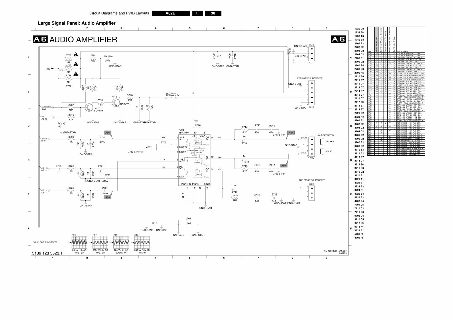
38A02E 7.Circuit Diagrams and PWB Layouts
A
B
C
D
E
F
1735 D81738 E8
1739 A81740 B8
2701 E32702 E2
2703 C22704 D2
2705 D12706 D2
2707 B42708 D3
2709 A62710 A6
2711 D72712 D7
2713 D72714 C7
2715 C72716 C7
2717 E62718 E7
2719 E72721 D2
2722 A3
9
9
3701 E2
3702 E23703 C2
3704 D23705 D2
3706 D23707 B2
3708 B23710 B3
3711 B2
3713 D73714 C7
3715 E63716 B3
3719 C23720 A1
3721 A13722 B1
3723 B23724 C1
3725 B43726 A2
4702 D4
10W 8E R
7701 C5
7710 C27711 B3
9702 D49710 C5
9712 E59715 F4
9722 B1c701 F5
c702 F5
10W 8E L
MAIN SPEAKERS
BWOOFER
.
SUBWOOFER
5
38
40
39
CL 36532058_048.eps030903
Item 2x10
W w
/o H
P A
mp
3x10
W w
/o H
P A
mp
+ S
ubw
oofe
r
2x10
W w
ith E
XT
Sub
woo
fer
3x10
W w
ith H
P a
mp
+ S
ubw
oofe
r
2x10
W w
ith H
P A
mp
DESCRIPTION1738 --- V --- V --- CON BM V 3P M 2.50 EH B1739 --- --- V --- --- CON BM V 3P M 2.50 EH B2701 V --- V --- V CER2 0805 Y5V 16V 1U COL R2701 --- V --- V --- CER2 0603 X7R 16V 100N COL2702 V V V V V CER1 0603 NP0 25V 1N COL2703 V --- V --- V CER2 0805 Y5V 16V 1U COL R2703 --- V --- V --- CER2 0603 X7R 16V 100N COL2704 V V V V V CER1 0603 NP0 25V 1N COL2705 --- V --- V --- CER2 0805 Y5V 16V 1U COL R2706 --- V --- V --- CER2 0603 X7R 50V 3N3 COL2711 V --- V --- V ELCAP 25V S 1000U PM20 COL B2711 --- V --- V --- ELCAP 25V S 470U PM20 COL B2714 V --- V --- V ELCAP 25V S 1000U PM20 COL B2714 --- V --- --- --- ELCAP 25V S 470U PM20 COL B2715 V V V V V CER2 0603 X7R 16V 47N COL2716 V V V V V CER2 0603 X7R 16V 47N COL2717 --- V --- V --- ELCAP 25V S 1000U PM20 COL B2718 --- V --- V --- CER2 0603 X7R 16V 47N COL2719 --- V --- V --- CER2 0603 X7R 16V 47N COL2721 --- --- --- V --- CER2 0603 X7R 10V 220N COL2721 --- V --- --- --- CER2 0603 Y5V 10V 470N COL2751 --- --- --- V V CER2 0805 Y5V 50V 100N P8020 R2752 --- --- --- V V ELCAP 25V S 100U PM20 COL A2753 --- --- --- V V CER2 0805 Y5V 50V 100N P8020 R2754 --- --- --- V V CER2 0805 Y5V 16V 1U COL R2755 --- --- --- V V ELCAP 25V S 100U PM20 COL A2756 --- --- --- V V CER1 0603 NP0 50V 33P COL2757 --- --- --- V V CER2 0603 X7R 16V 100N COL2758 --- --- --- V V CER2 0805 Y5V 16V 1U COL R2759 --- --- --- V V ELCAP 25V S 100U PM20 COL A2760 --- --- --- V V CER1 0603 NP0 50V 33P COL2761 --- --- --- V V CER2 0603 X7R 16V 100N COL2762 --- --- --- V V CER1 0603 NP0 25V 1N COL2763 --- --- --- V V CER1 0603 NP0 25V 1N COL2764 --- --- --- V V ELCAP 10V S 470U PM20 COL A3703 V V V V --- RST SM 0603 10K PM5 COL3703 --- --- --- --- V RST SM 0603 18K PM5 COL3704 V V V V --- RST SM 0603 22K PM5 COL3704 --- --- --- --- V RST SM 0805 10K PM5 COL R3705 --- V --- V --- RST SM 0603 10K PM5 COL3706 --- V --- --- --- RST SM 0603 22K PM5 COL3706 --- --- --- --- V RST SM 0805 10K PM5 COL R3706 --- --- --- V --- RST SM 0805 22K PM5 COL R3715 --- V --- V --- RST SM 0603 RC21 8R2 PM5 R3722 --- V --- V --- RST FUSE NFR25 S 1R PM5 A3751 --- --- --- V V RST SM 0603 22K PM5 COL3752 --- --- --- V V RST SM 0603 47K PM5 COL3753 --- --- --- V V RST SM 0603 47K PM5 COL3754 --- --- --- V V RST CRB CFR25S A 3R9 PM5 A3755 --- --- --- V V RST SM 0603 12K PM5 COL3756 --- --- --- V V RST SM 0603 12K PM5 COL3757 --- --- --- V V RST SM 0603 100K PM5 COL
1 2 3 4 5 6 7 8
F
* ONLY FOR SUBWOOFER
GND-STAR GND-SSP
GND-AUD GND-STAR
3139 123 5523.1
A56
20mV / div AC1ms / div
A57
500mV / div AC1ms / div
A58
20mV / div AC200µs / div
A59
500mV / div AC1ms / div
Large Signal Panel: Audio Amplifier
CENTER
OPAMP
OPAMP
OPAMP
L/R
MUTE/STBYPROTECT
PGND
A8-
19
1 2 3 4 5 6 7 8
A
B
C
D
E
A8-2
SPK-L
AUDIO AMPLIFIER
A8-14
14V
A8-19
A8-45
14V
50K
32V
SPK-R
14V
14V
14V
NORMAL = 0VMUTE = 5V
14V
FOR ACTIVE SU
32V
N.C
*
*
A8-13
FOR PASSIVE
3702
10K
2712
47n
3
4
5
9715
1R
3720
GND-STAR
1n 2702
1731
2
3
4
9710
9712
2701
220n
470u
2708
GND-STAR
3705
1K
9702
47n
2715
3719
47K
GND-STAR
1R
3716
10K
1u
2705
3723
2703
220n
GND-STAR
1m2709
GND-STAR
3722
2710
100n GND-STAR
GND-STAR
3715
4R7
GND-STARGND-STAR
1n 2704
GND-STAR
47n
2716
c702
10K
3725
BC847B7710
171
2
3
GND-STAR
4R7
3713
GND-STAR
2713
47n
GND-STAR
GND-STAR
3707
10K
GND-STAR
10K
3724
1K
37031u 27
07
47K
3708
BC847B
7711
9722
171
2
GND-STAR
27061n
INL
1 INR
10 MUTE1
9 MUTE2
OC 3
12OL
14OR
PGND-C
4 11 15 8
SGND
7 SVR
13
VS
2
VS-C
TDA74977701
INC6
5
3714
4R7
47n
2718
171
2
3
2721
1u
2722
100u50V
GND-STAR
3726
10K
47n
2719
10K
3706
GND-STAR
2711
1m
3711
10K
3710
47K
1K
3701
GND-STAR
1m
2714
A56
1m
2717
A57
3704
10K
GND-STAR
A58
A59
c701
4702
GND-STAR
1R
3721
AU
DIO
-SW
GND-STAR
+28V
AUDIO-L
AUDIO-SW
AUDIO-R
SOUND-ENABLE
POR
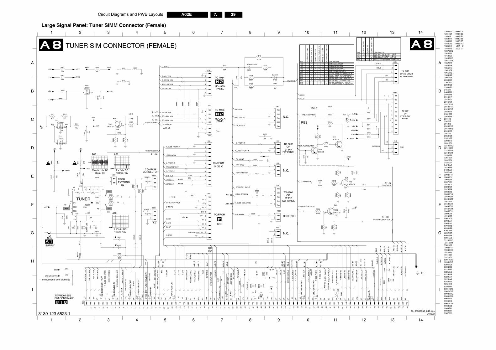
Circuit Diagrams and PWB Layouts 39A02E 7.
*
HA
VA
SDA-S
SCL-S
+5V
+8V
SUPPLY
8V1
1V1
0V 0V 0V 4V5
4V5
0V 0V 0V 0V 4V3
3V5
3V6
3V5
0V 3V1
3V3
3V
A11-66
A11-68
-41
A11
-74
A11
-72
A11
-73
N.C
A6-
19
A6-
13
A6-
14
A10
-27
A10
-24
A10
-25
.--. A11
TO 1951
NOT EUR
NOT EUR
A7-
34
A7-
35
A1-
30
OF 3D-COMBFILTER PANEL
TO 0201OF
2T PIP/DWPANEL
12 13 14
12 13 14
A
B
C
D
E
F
G
H
I
1200 F21201 G11205 I21932 F91933 B61934 A61935 E91936 D61937 B131940 F61943 E51948 D131951 A131952 E91953 D91955 F51961 C91965 D61966 G91997 E32200 D22201 F12202 G22203 G32455 I72483 B92496 B82914 E22915 E12916 C42917 E122918 F112929 E102930 F82931 D92940 B32941 I82942 I82943 I82944 E122945 H132946 I132947 I72950 G32951 G23200 F33201 F33210 D103211 D103212 D113213 C113250 H33261 E43262 F43427 A73428 A83429 B83430 A93432 A83903 F113904 E13905 I113907 C13910 C13928 C43929 D43930 D33938 F103939 G113940 G113941 E23942 E113943 E113944 C113945 F113999 A34915 I115901 C25902 A15903 A15904 H86200 G26201 G36202 G36402 B96901 A87210 D107211 D117901 C37902 F117908 E117910 B27911 D17912 C19201 C129203 C129205 E89206 D89215 G29225 E89226 D99228 A49229 A49250 E69251 E69292 B49901 C129902 C129903 D129904 C129905 F89906 E39907 C119908 C39909 B19980 B19982 F6
9983 C119987 B69988 B69989 B69990 B59998 I13c001 H2c002 I2
N.C.
-41
9998
10K
220n
2944
9998
10K
3944
100n
2918
2917
100n
2946
2u2
2945
2u2
9904
9203
9903
9902
9901
9201
19481
2
3
9
19511
2
3
4
5
19371
10
2
3
4
5
6
7
8
7908
3903
560R
BC847B
2K7
6202
79 80
GN
D-A
UD
65 66 67 68 69 70 71 72 73 74 75 76 77 7864
+11V5
AUDIO-SL
+5.2V
+8VS
SC2-CVBS_MON-OUT
+8VS2
SC2-C-OUT
+5VA
VTUN
AU
DIO
-L
AU
DIO
-R
+8V
HE
AD
PH
ON
E-L
HE
AD
PH
ON
E-R
C-F
RO
NT-
IN
L-F
RO
NT-
IN
R-F
RO
NT-
IN
L-C
L_V
L-O
UT
R-C
L_V
L-O
UT
AU
DIO
-SL
AU
DIO
-C
AU
DIO
-SW
ON
-OF
F-L
ED
RC
KE
YB
OA
RD
DE
GA
US
SIN
G
CL 36532058_042.eps040903
Item. SC
AR
T I/
O +
SC
3
SC
AR
T I/
O
SC
AR
T I/
O+
SC
3+ P
IP
DESCRIPTION1937 --- --- CON BM V 10P M 2.50 EH B1951 --- CON BM V 5P M 2.50 EH B9203 --- --- RST SM 0603 JUMP. 0R05 COL9902 --- --- WR CU-ETP SNPB5-PL 0.58MM COL
00A0A0A8BA I X-3 I X U-30U PM20 COL A7U PM20 COL A0K PM5 COL RP. 0R05 COL R0R PM5 COL16 (COL) R5-PL 0.58MM COL
vvvvv
GN
D-S
CA
RT-
AV
GN
D-S
CA
RT-
AV
GN
D-R
GB
-CR
T
GN
D-P
IP
GN
D-C
VB
S-O
UT
GN
D-R
GB
-SC
1_Y
UV
GN
D-C
VB
S-I
N
CV
BS
-PIP
_TU
N1-
2-C
VB
S-I
N
* components with diversity
TO/FROM SSBSIM CONN MALE
GN
D-C
VB
S-O
UT
0V 0V 0V 0V
0V
0V 0V
0V
0V2V7
2V7
0V
0V
0V 4V1
0V
0V 0V 3V2
5V7
0V
3V 3V 3V
2V5
0V 1V1
0V9
0V 1V6
6V 4V 2V3
0V 0V 0V 5V2
2V8
0V
8V1
3V5
5V1
3V5
3V5
3V2
5V 5V 0V 0V 0V 0V 0V
0V
0V 0V
0V
0V 0V 0V 0V8
0V
A2-
47
A11
-59
A8-
61
A11
-69
A11
-67
A3-
3
A3-
4
A4-
10
A4-
11
A3-
20
A4-
6A
4
A5-
49
A2-
9
A10
-31
A3-
45
A6-
2
A11
-55
A11
-65
A11
-81
A11
-57
A11
-64
A11
-82
A11
-56
2V6
1V4
1 2 3 4 5 6 7 8 9 10 11
H
I
A3
A6-
45
A11
-58
1n2455
100R
3XX
X
83R
5904
2947
4u7
2943
100n
100n
2941
2942
100n
22K
3250
c002
c001
8 97 50 51 52 53 54 55 56 57 58 596 60 61 62 6336 37 38 394 40 41 42 43 44 45 46 47 48 495 21 22 23 24 25 26 27 28 293 30 31 32 33 34 351 10 11 12 13 14 15 16 17 18 192 20
1205
+5V
VT
UN
LIG
HT-
SE
NS
OR
+5VA
SC
L-S
SD
A-S
GN
D
FR
AM
ED
RIV
E-
FR
AM
ED
RIV
E+
GN
D-L
INE
DR
IVE
LIN
ED
RIV
E1
+3V3
GND
GND-LINEDRIVE
STA
ND
BY
PO
R
Y_C
VB
S-F
RO
NT-
IN
+3V3
+8V
Y-S
CA
VE
M
+5.
2V
IRQ
-DIG
ITA
L
DY
N-F
AS
E-C
OR
EW
-DR
IVE
R-S
C2-
OU
T
Y_C
VB
S-S
C2_
AV
2-IN
R-S
C1_
AV
1-IN
R-S
C1_
AV
-OU
T
FR
ON
T-D
ET
EC
T
C-S
C2_
SV
HS
-IN
CV
BS
-SC
2_M
ON
-OU
T
B-S
C1-
IN_U
-IN
CV
BS
-SC
1_A
V1-
IN
CV
BS
-TE
R-O
UT
IF-T
ER
AG
C
PIP
-CV
BS
SC
1-S
TAT
US
SE
L-S
VH
S-R
R_S
TAT
US
2
G-S
C1-
IN_Y
-IN
P50
CU
TOF
F
B-C
RT
G-C
RT
R-C
RT
R-S
C1_
V-I
N
HF
B_X
-RAY
-PR
OT
EH
T-IN
FO
TIL
T
PIP
-MO
NO
FB
L-S
C1-
IN
SO
UN
D-E
NA
BLE
L-S
C1_
AV
1-IN
L-S
C2_
AV
2-IN
L-S
C2-
OU
T
L-S
C1_
AV
-OU
T
R-S
C2_
AV
2-IN
3139 123 5523.1
Large Signal Panel: Tuner SIMM Connector (Female)
NC GND
*
*
TUNER SIM CONNECTOR (FEMALE)
TO/FROM
TO/FROM
TO
TUNER
SDA-S
SCL-S
SDA-S
SCL-S
COMPAIRCONNECTOR
1510
CRT
SIDE IO
FM
FROMEXTERNAL
FM
N.C.
N.C.
RESERVED
TO 1934
1V7
2V7
8V1
2V7
8V1
3V
2V4
4V97V5
0V
0V
5V
5V
4V9
1V7
4V9
2V2
0V
0V
6V
2V8
3V
3V
3V
0V
5V7
8V4
33V
A11-53
A11-52
A11-51
A11-54
A11-60
A7-37
A7-38
A11-70
A11-71
GND-RGB-CRT
N.C.
HD JACKPANEL
TO 1933
HD JACKPANEL
TO 0200
2T PIPDW PANEL
OF
TO 0236
2T PIPDW PANEL
OF
N.C.
N.C.
RES
1 2 3 4 5 6 7 8 9 10 11
A
B
C
D
E
F
G
1933
7902
BC847B
19521
2
3
A69
9982
1
2
3
4
19651
2
3938
100R
1
2
1997
3904
6R8
9251
100R
3261
3262
100R
47R
3907 3910
68R
2950
10n
9990
9292
9228
9226
9229
100K
3432
9225
2496
10n
3429
100K
56K
3427
BAS316
6402
4n7
2483
3428
330K
BZX384-C5V6
6901 100K
3430
1n
2930
F921
1n
2931
1K
3999 F922
2K2
3211
15R
3213
1K3210
100R
3212
7211
BC847B
BC847B
7210
9980
GNDIN OUT
9909
10n
2951
L78L057911
MC78M057912
GNDIN OUT
33u
5903
33u
5902
2916
330p
9908
9250
10u
5901
1966
1
2
9907
9906
9905
1
2
3
4
5
1961
A70A68 19551
2
3
1
2
9215
1932
1
2
3
10
11
2
3
4
5
6
7
8
9
1943
2
3
4
5
6
19401
1
2
3
4
5
19341
1
2
3
1935
1953
2915
10u
2940
100u
LD10867910
GNDIN OUT
19361
10
11
2
3
4
5
6
7
8
9
7901
BC847B
9205
9206
100R
3942
3945
3943
2929
220n
3939
10K
560R
3940
6R8
3941
9983
10u
2914
9987
9988
9989
10K
3929
100R
3928
560R
3930
6201
1201 1
3201
100R
2203
100u
100R
3200
220n
2201
10u
2200
2202
220n
BZ
M55
-C33
6200
11IF1
6MB1
MB27
12131415
2
810
4SCL
5SDA
9
TU2
TEDE91200
1 AGC
3AS
+8V6 +8V
+11V +11V5
+5.2V
PROT_AUDIOSUPPLY
+8V
EHT-INFO
EW-DRIVE
GND
+8V
GND-AUD
+3V3
+8VS2
+8V
+8V+5VT
AUDIO-SL
R-CL_VL-OUT
L-CL_VL-OUT
PANORAMA
VTUN
SC
L-S
SD
A-S
+5V
+11V5
Y_CVBS-FRONT-IN
PIP-CVBS
SC1-FBL-IN
TER-CVBS-OUT
HFB_X-RAY-PROT
+8VS
+8V
CVBS-SC2_MON-OUT
C-FRONT-IN
PIP-MONO
+8VS
CVBS-TER-OUT
HEADPH-R
HEADPH-L
SC1-R_V-IN
SC1-G-IN_Y-IN
SC1-B-IN_U-IN
TER-CVBS-OUT
SD
A-S
CVBS-SC1_AV1-IN
C-SC2_SVHS-IN
Y_CVBS-SC2_AV2-IN
C-FRONT-IN
B-SC1-IN_U-IN
FBL-SC1-IN
HFB_X-RAY-PROT
Y_CVBS-FRONT-IN
FRONT-DETECT
C-FRONT-IN
L-FRONT-IN
R-FRONT-IN
SDA-S
SCL-S
+5VT
SC
L-S
R-SC1_V-IN
G-SC1-IN_Y-IN
EHT-INFO
R-CRT
G-CRT
B-CRT
CUTOFF
+8V
A68
500mV / div AC20µs / div
A69
2 V / div DC100ms / div
A70
2 V / div DC100ms / div
Item EU
CE
NE
LEC
LL3
8.9
NA
NT
SC
FP
IN 4
5.75
Chi
na IE
C P
AL
38.0
NA
NT
SC
PH
ON
O 4
5.75
AP
PA
L 38
.9 n
on-P
IP
EU
CE
NE
LEC
LL3
8.9
PIP
DESCRIPTION1200 --- --- --- --- --- TUNER TEDH9X71200 --- --- --- --- --- TUNER TEDE9-201200 --- --- --- --- --- TUNER TEDH9-241200 --- --- --- --- --- TUNER TEDE9-221200 --- --- --- --- --- TUNER UV1316T/1200 --- --- --- --- --- TUNER UV1317/A2203 --- --- ELCAP 10V S 102203 --- --- --- --- ELCAP 25V S 43250 --- --- --- --- RST SM 0805 13250 --- --- RST SM 0805 JUM3905 --- --- --- --- --- RST SM 0603 106202 --- --- --- --- DIO SIG SM BAS39925 --- --- --- --- WR CU-ETP SNPB
v
v
v
v v v v
vv
v
v
v
vv
v
v
v
v
v
v
vvv
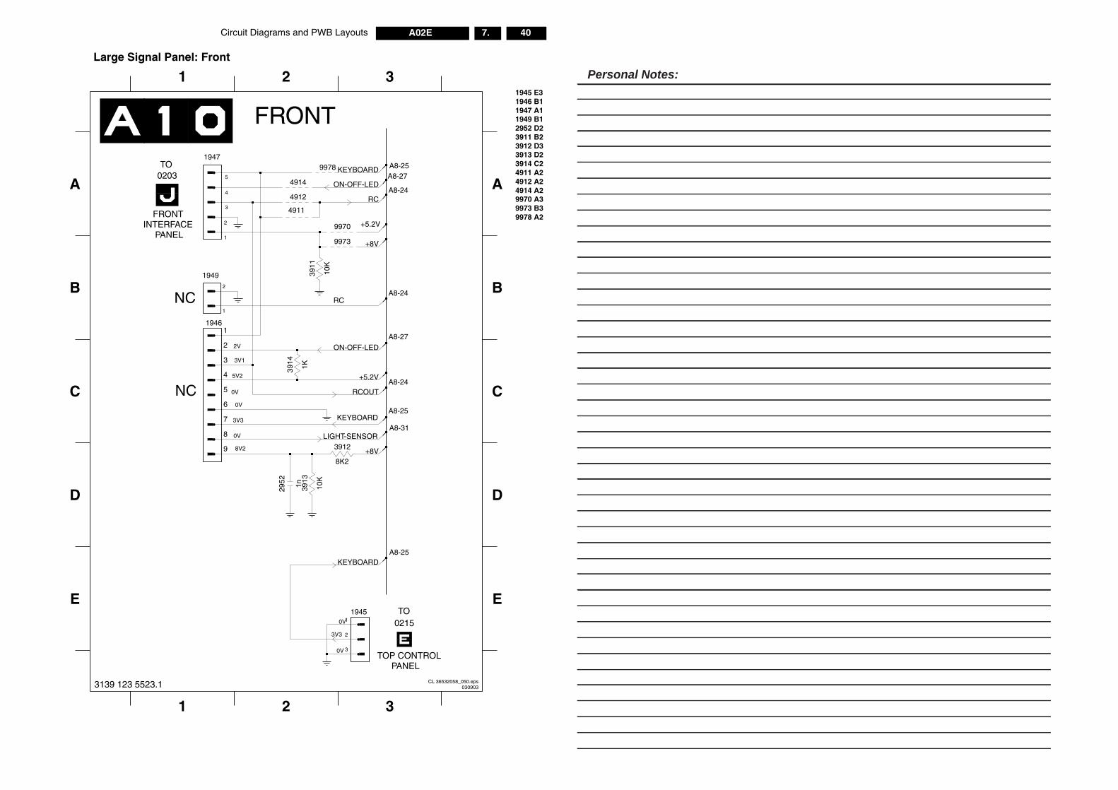
40A02E 7.Circuit Diagrams and PWB Layouts
A8-25KEYBOARD
TO0215
TOP CONTROLPANEL
0V
0V
3V3
1 2 3
E E1945
1
2
3
CL 36532058_050.eps0309033139 123 5523.1
Large Signal Panel: Front
FRONT
NC
0V
0V
0V
2V
3V1
5V2
3V3
8V2
A8-27
A8-24
A8-24
A8-27
A8-24
A8-25
A8-31
1 2 3
A
B
C
D
A
B
C
D
1945 E31946 B11947 A11949 B12952 D23911 B23912 D33913 D23914 C24911 A24912 A24914 A29970 A39973 B39978 A2
A8-25TO0203
PANELINTERFACE
FRONT
NC
1
2
1949
1946
9973
1n2952
4911
4914
3914
1K
8K2
3912
4912
10K
3913
10K
3911
9970
9978
1
2
3
4
5
6
7
8
9
1947
1
2
3
4
5
ON-OFF-LED
RC
RCOUT
ON-OFF-LED
+5.2V
KEYBOARD
LIGHT-SENSOR
+8V
RC
KEYBOARD
+8V
+5.2V
Personal Notes:
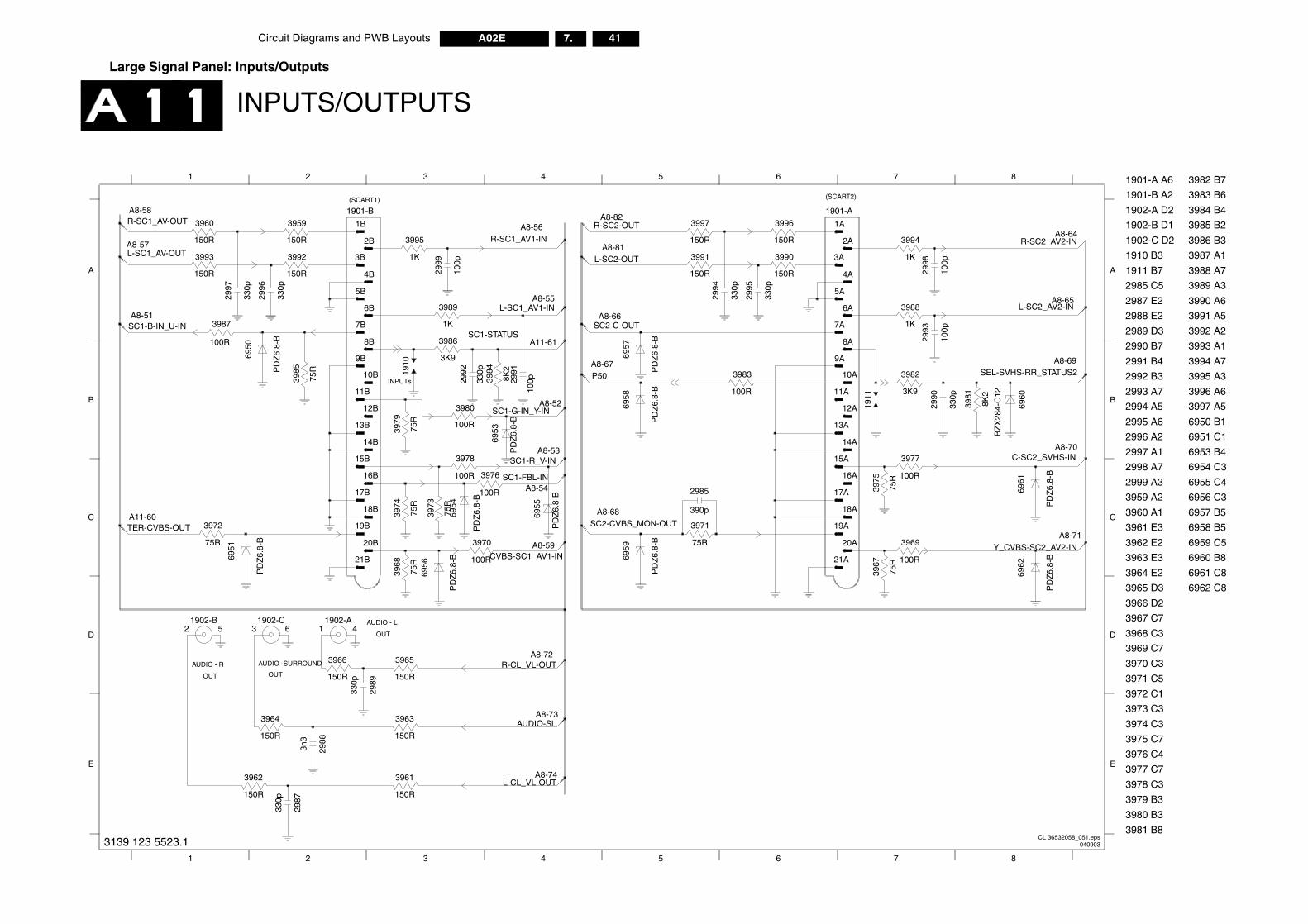
Circuit Diagrams and PWB Layouts 41A02E 7.
A8-72
A8-64
A8-65
A8-69
A8-70
A8-71
8
8
A
B
C
D
E
1901-A A6
1901-B A2
1902-A D2
1902-B D1
1902-C D2
1910 B3
1911 B7
2985 C5
2987 E2
2988 E2
2989 D3
2990 B7
2991 B4
2992 B3
2993 A7
2994 A5
2995 A6
2996 A2
2997 A1
2998 A7
2999 A3
3959 A2
3960 A1
3961 E3
3962 E2
3963 E3
3964 E2
3965 D3
3966 D2
3967 C7
3968 C3
3969 C7
3970 C3
3971 C5
3972 C1
3973 C3
3974 C3
3975 C7
3976 C4
3977 C7
3978 C3
3979 B3
3980 B3
3981 B8
3982 B7
3983 B6
3984 B4
3985 B2
3986 B3
3987 A1
3988 A7
3989 A3
3990 A6
3991 A5
3992 A2
3993 A1
3994 A7
3995 A3
3996 A6
3997 A5
6950 B1
6951 C1
6953 B4
6954 C3
6955 C4
6956 C3
6957 B5
6958 B5
6959 C5
6960 B8
6961 C8
6962 C8
BZ
X28
4-C
12
6960
PD
Z6.
8-B
6962
6961
PD
Z6.
8-B100R
100R
3969
3977
8K2
3981
2990
330p
3982
3K9
100p
2993
2998
100p
1K
3988
3994
1K
R-SC2_AV2-IN
L-SC2_AV2-IN
SEL-SVHS-RR_STATUS2
Y_CVBS-SC2_AV2-IN
C-SC2_SVHS-IN
CL 36532058_051.eps040903
AUDIO - R
OUT
AUDIO -SURROUND
OUT
A8-73
A8-74
1 2 3 4 5 6 7
E
2988
3n3
330p
2989
2987
330p
150R
39613962
150R
3963
150R
150R
3965
150R
3964
3966
150RR-CL_VL-OUT
AUDIO-SL
L-CL_VL-OUT
3139 123 5523.1
Large Signal Panel: Inputs/Outputs
(SCART2)(SCART1)
AUDIO - L
OUT
INPUTs
INPUTS/OUTPUTS
A8-58
A8-57
A8-51
A11-60
A8-56
A8-55
A11-61
A8-52
A8-53
A8-54
A8-59
A8-82
A8-81
A8-66
A8-67
A8-68
1 2 3 4 5 6 7
A
B
C
D
1901-A
1A
11902-A
4
3980
100R
3987
2985
390p
3971
75R
3993
150R
1910
6951
PD
Z6.
8-B
1911
PD
Z6.
8-B
6950
6953
PD
Z6.
8-B
PD
Z6.
8-B
6955
PD
Z6.
8-B
6954
6956
PD
Z6.
8-B
6957
PD
Z6.
8-B
6958
6959
PD
Z6.
8-B
PD
Z6.
8-B 100R
3983
3970
100R
3976
100R
100R
100R
3978
3991
150R
2994
330p
150R
3997
330p
2995
3996
150R
150R
3990
3967
75R
75R
3975
4A
5A
6A
7A
8A
9A
10A
11A
12A
13A
14A
15A
16A
17A
18A
19A
2A
20A
21A
3A
521902-C
631902-B
3972
75R
150R
3960
2999
100p
100p29
91
1K
398975
R
3985
330p
8K2
3984
3K9
3986
2992
3979
75R
75R
3973
3974
75R
75R
3968
2997
330p
1K
3995
330p
2996
3992
150R
20B
21B
3B
4B
5B
6B
7B
8B
9B
150R
3959
1901-B
1B
10B
11B
12B
13B
14B
15B
16B
17B
18B
19B
2B
SC1-B-IN_U-IN
SC1-G-IN_Y-IN
SC1-R_V-IN
CVBS-SC1_AV1-IN
SC1-FBL-IN
R-SC1_AV1-IN
SC1-STATUS
L-SC1_AV1-IN
TER-CVBS-OUT
R-SC1_AV-OUT
L-SC1_AV-OUT
SC2-C-OUT
SC2-CVBS_MON-OUT
R-SC2-OUT
L-SC2-OUT
P50
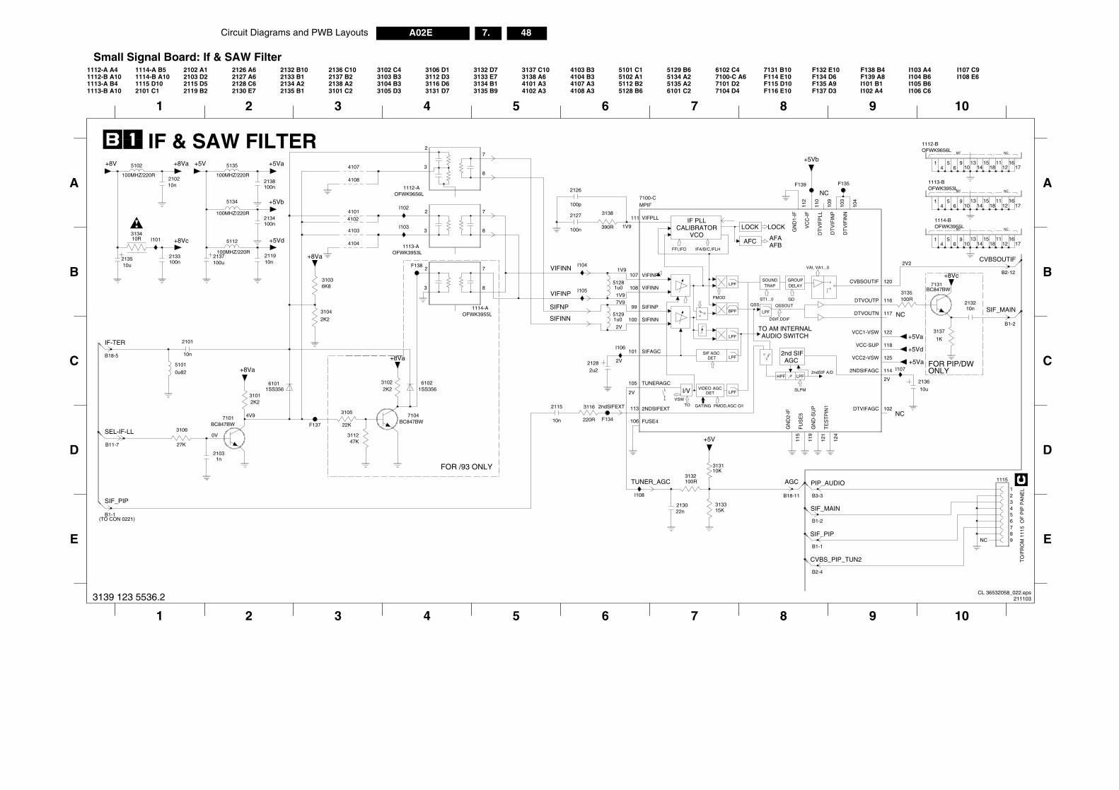
48A02E 7.Circuit Diagrams and PWB Layouts
NCMT
NCMT
NCMT
AGC
HPF
AFAAFB
OCK
APGROUPDELAY
LPF2ndSIF A/D
SLPM
QSSOUT
DSIF,DDIF
..0 GD
VAI, VA1...0
DIO SWITCHAM INTERNAL
ND
2nd SIF
C
D
B
A
9
8 9 10
I108 E6
ENC
TO
/FR
OM
111
5 O
F P
IP P
AN
EL
10
B18-11
NCB1-2
B1-1
B1-2
B2-4
NC
B3-3
NC
B2-12
8
31 B1014 E10
2V2
2V
FOR PIP/DWONLY
I101 B1I102 A4
I103 A4I104 B6I105 B6I106 C6
I107 C9
15 D1016 E10
F132 E10F134 D6F135 A9F137 D3
F138 B4F139 A8
1415 11
1216
17
OFWK3955L1114-B
1184
56
910
13
45
69
1013
1415 11
1216
17
1617
1113-BOFWK3953L
118
1184
56
910
1314
15 1112
OFWK9656L1112-B
+8Vc
213210n
3137
1K
100R3135
7131BC847BW
789
2136
10u
123456
F139
1115
+5Vd
+5Va
+5Vb
I107
F135
TE
ST
PIN
1
124
VC
C-I
F
110
VCC-SUP 118
VCC1-VSW 122
VCC2-VSW 125
2NDSIFAGC 114
CVBSOUTIF 120
DTVIFAGC 102
DT
VIF
INN
104
DT
VIF
INP
103
DT
VIF
PLL
109
DTVOUTN 117
DTVOUTP 116
FU
SE
5
119
GN
D-S
UP
121
GN
D1-
IF
112
GN
D2-
IF
115
+5Va
SIF_PIP
CVBS_PIP_TUN2
SIF_MAIN
AGC
CVBSOUTIF
PIP_AUDIO
SIF_MAIN
CL 36532058_022.eps211103
4 5 6 71 32
3139 123 5536.2
Small Signal Board: If & SAW Filter
IF PLLCALIBRATOR
VCO
LPF
SIF
I/V
BPF
LPF
LPFAGC
DET
VSWTO
VIDEOLPF
LPF
AFC
L
TR
PMOD
QSSST1.
AUTO
LOCK
SOU
AGCDET
PMOD,AGC O/IGATING
FFI,IFO IFA/B/C,IFLH
F138
5101 C15102 A1
100MHZ/220R
5112 B21113-B A10
1114-A B51114-B A101115 D10
A
2132 B10
6101 C2
6102 C4
2134 A2
2136 C10
2135 B1
2137 B22133 B11112-A A41112-B A10
2101 C1
2102 A12103 D22115 D52119 B2
2126 A62127 A62128 C6
B
C
D
E
7100-C A6
2130 E7
IF & SAW FILTER
3132 D74104 B3
4102 A33116 D63112 D3
3131 D7
4103 B33133 E7
B18-5
4101 A33104 B33105 D3
3106 D1
4108 A34107 A3
B11-7
(TO CON 0221)
100MHZ/220R
100MHZ/220R
100MHZ/220R
B1-1
3101 C2
3102 C43103 B3
3137 C103138 A6
3134 B13135 B9
5 6 7
7101 D27104 D4
71F1
2138 A25128 B6
2V
2V
2V
5129 B6
F1F1
1 2 3 4
1113-A B45134 A25135 A2
4V9
0V
FOR /93 ONLY
1V9
1V9
1V97V9
2K2
3104
213510u
4107
+5Vd+8Vc
+8V +8Va
+8Va
7101
3106
27K
BC847BW
211910n100n
2133
5112
313410R
100n
2127
6102
+5V
2K23101
1SS356
21031n
22n2130
I102
+5V
I101
1u05128
2126
100p
3
7
8
+8Va
F137
3138
390R
OFWK3955L1114-A
2
10n
2101
3132100R
+5Vb
15K3133
4102
+5Va
4108
21282u2
6K8
5101
0u82
5102
3103
100n2138
100u2137
I108
4101
I106
I105
3
7
8
4104
I104
2
3
7
8
OFWK9656L1112-A
2
2115
10n
1113-AOFWK3953L
313110K
51291u0
I1034103
5134
2134100n
210210n
47K3112
BC847BW7104
3105
31022K2
22K
5135
1SS356
220R
3116
+8Va
6101
SIFAGC101
SIFINN100
SIFINP99
TUNERAGC105
VIFINN108
VIFINP107
VIFPLL111
F134
2NDSIFEXT113
FUSE4106
7100-CMPIF
SIF_PIP
2ndSIFEXT
VIFINN
VIFINP
IF-TER
SEL-IF-LL
TUNER_AGC
SIFINN
SIFNP
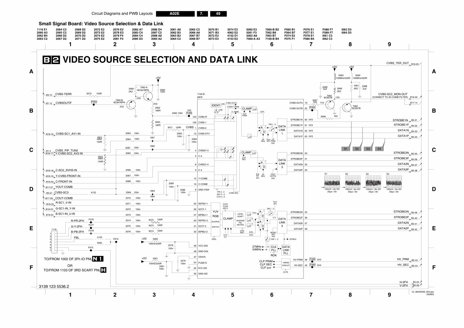
Circuit Diagrams and PWB Layouts 49A02E 7.
MONODVDMAT ICPL
BC857B7062
8
D
F
B5-25
9
F088 F7F089 F7I061 C3I062 C3
I063 D3
8
I064 D3
E
B5-40
100MHz/220R 100MHz/220R
9
E
A
B
C
B5-44
B5-33
B18-30
B17-14
B5-38
B5-31
B5-34
B5-36
B5-35
B5-37
B18-29
B5-26
B5-32
B5-43
B5-39
B5-41
B5-42
(CONNECT TO 3D COMB FILTER)
1V4
1V9
3
4
2K23066
S1 S2 S3 S4
F078
2u22088
1K03068
+5V
5063
B|PB|U-232100R30742076
30612K2
100n1
7063BC857B
2u22082
+5V
5062
H-2FHV-2FH
CVBS-SC2_MON-OUT
CVBS_TER_OUT
STROBE2P
DATA2N
DATA2P
HV_PRM
HV_SEC
B-PB-2FH
STROBE1N
STROBE1P
DATA1N
DATA1P
STROBE3N
STROBE3P
DATA3N
DATA3P
STROBE2N
CL 36532058_023.eps030903
S1
100mV / div DC20µs / div
S2
100mV / div DC20µs / div
S3
100mV / div DC20µs / div
S4
100mV / div DC20µs / div
SECDIG
CLPyuv
ICPL
RSEL
DATALINK54MHz
DM 1...0 297MHz
PLL
CIRCUIT
CLP PRIMCLP SECCLP yuv
CLPS
CLKPLL
27MHz
TIMING
ROK
1 2 3 4 5 6 7
F
100HZ/220R
100HZ/220R
TO/FROM 1002 OF 2Fh IO PNL
ORTO/FROM 1103 OF 3RD SCART PNL
0V
0V
2078100n
+5V
F089
F088
4062
4153
46HV-PRIM
45HV-SEC
49 VCC-DIG
64 VCC-I2D
47 VD2V5
54 FUSE10
48 GND-DIG
59 GND-I2D
5061
5060
2079100n
2081100n
+5V
234567
F074
F075
FBL
3139 123 5536.2
Small Signal Board: Video Source Selection & Data Link
VIM
CVBS/Y PRIM
C- PRIMCLPPRIM
LPF
SEC 3...0CVO 3...0
CVBS SEC
CLAMP LPF
CLPSEC
A
D
ICPL
DM 1...0
PRIMLR
DIG2FhYyuv
MHz54
DATALINK
3
MHz54
SIF2nd
A/DHV-P/STEST
DIG
DATALINK
3
RGB
SOURCE
SWITCH
CLAMP
HDTVCLONCLPS
LEVELADAPT
INVERSEPAL
MATRIX
LPF
LPF
LPF
A
D
A
D
DM 1...0
U,VU
V
Yyuv
Yyuv2Fh
YUV
IDENTVID CVBS-OUTA
CLAMP LPF
A
D
+
PRI 3...0
DATALINK
1
100n
2085
B1-12
76543
B1-4
2060 A32062 B42063 C2
2064 C22065 C22066 D22067 D2
21
F078 E1F080 B4
A
1116 E1
RES
B17-28
B17-27
B18-22
B18-18
RES
2073 E22079 F42074 E2
2075 E2
2076 E22078 E3
B3-15
2082 A7
2084 C4
B
C
D
B18-17
4153 E2
5061 F35063 A87060-A A3
7060-B B27062 B87063 B7
2081 F3 7100-B B4
2083 C4F060 B1
2085 D3
2086 D42087 C22088 A83060 A2
3061 A83062 B33063 B33064 C2
3065 C23066 A83067 B73068 B7
3070 B13071 B33072 E33073 E3
3074 E34062 E24152 D1
5060 E3
B18-20
VIDEO SOURCE SELECTION AND DATA LINK
B3-21
B18-19
2068 D22069 D22070 D22071 D2
2072 E2
B18-16
B18-23
B18-24
2V8
2V22V2
1V6
0V3
0V3
0V3
0V3
F064 B7F074 E2F075 F1
F076 E1F077 E1
3072 100R
150R3065
100n2083
2084100n
F080
F076
F077
100n2063
7060-BBC847BPN
100n
100n2075
100n2073
2074
2072 100n
100n2069
3063180R
7060-ABC847BPN
1K03067
100n2067
4152
100n2070
3064150R
100n2087
100R3071
100n
100n2068
25 R|PR|V-1
R|PR|V-230
60STROBE1N
61STROBE1P
56STROBE2F
55STROBE2N
50STROBE3N
51STROBE3P
15 Y-COMB
2065
19CVBS-OUTA
22CVBS-OUTB
4 CVBS|Y-3
8 CVBS|Y-4
62DATA1N
63DATA1P
57DATA2N
58DATA2P
52DATA3N
53DATA3P
6 GND-VSW
26 G|Y|Y-1
G|Y|Y-231
MPIF7100-B
27 B|PB|U-1
5 C-3
9 C-4
16 C-COMB
126 CVBS-1
1 CVBS-2
12 CVBS-DTV
123 CVBS-IF
100R3070
3073 100R
30602K2
100n2064
100n2071
I062
3062180R
2066 100n
I061
+5V
1116
2086100n
F064
F060
I063
I064
2062 100n
2060100n
YOUT-COMB
CVBS-SC3
CVBS-TERR
COUT-COMB
CVBS-SC1_AV1-IN
CVBS_PIP_TUN2
C-SC2_SVHS-IN
Y-CVBS-FRONT-IN
C-FRONT-IN
CVBS
G-SC1-IN_Y-IN
CVBSOUTIF
Y-CVBS-SC2_AV2-IN
R-SC1_V-IN
B-SC1-IN_U-IN
R-PR-2FH
G-Y-2FH
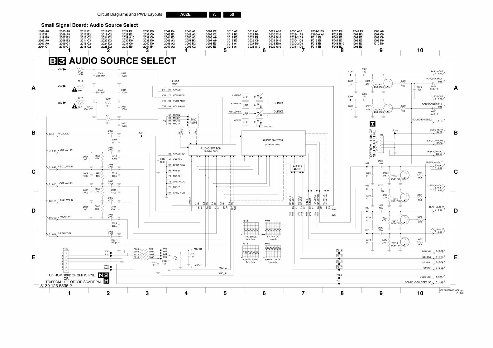
50A02E 7.Circuit Diagrams and PWB Layouts
I009
I010
6030BAS316
10u
TO
/FR
OM
110
4 O
F
8 9
B18
B18
B3-59
B10-65
B10-64
B10-63
B18-66
B18-61
B3-58
B18-67
B10-62
B2-21
8 9 10
10
B10
I010 D9
B3-58
B2-15
B18-60
B18-57
B18-56
A
B
C
D
E
E8E8E2E2B10E2
F047 E2I001 B3I002 E3I003 E3I004 E3I005 E3
I006 A8I007 C9I008 C9I009 D9
B11-53
3RD
SC
AR
T P
NL
B3-59
1K8
3029
BC847BS7029-2
47K3027
14
BC847BS7031-2
20061n
2038
F045
10u
1K8
3033
203910u
1n2033
I008
BAS3166029
1u02029
3028
1K87029-1
BC847BS
200310u
200210u
1009
I007
47K3024
3030
1K87030-1BC847BS
1K8
3031
BC847BS7030-2
3032
1K87031-1BC847BS
302647K
47K
2037
10u
3007
47K
3006
1118
12345
2040
15
I006
20321n
20301n
20311n
20
3022
21
1n
47K
17
2005SOUND-ENABLE_1
16
R-SC1_AV-OUT
L-SC1_AV-OUT
CVBS-SC3
SEL-2FH-SRC_STATUS3
L-CL_VL-OUT
R-CL_VL-OUT
L-SC1_AV-OUT
R-SC1_AV-OUT
L-SC2-OUT
R-SC2-OUT
SOUND-ENABLE_2
POR_FLASH_1
DSNDL2
DSNDR2
CVBS-TERR
DSNDL1
DSNDR1
CL 36532058_024.eps211103
F016 F017
I005
OR
4 5 6 72 31
TO/FROM 1062 OF 2Fh IO PNL
TO/FROM 1102 OF 3RD SCART PNL
E
F0
1nI004 2042
1117
1234567
100R
F047
3013
F046
20411n
I003I002
F0
3008 100R100R3012
F042F041
20441n1n
2043
F0
F0
F0
100R3009
F0
AUD-L1
AUD-R1
AUD_L2
AUD_R2
3139 123 5536.2
500mV / div DC1ms / div
500mV / div DC1ms / div
Small Signal Board: Audio Source Select
MIC
1
AM
LPF
LPF
LPF
AD
AD
AD
DLINK2MIC1/L2/PIPM
MIC2/R2
AUDIO SWITCH( ANALOG OUT )
AD
MICAMPS
AUDIO SWITCH( DIGITAL OUT )
AM
SO
UN
D
LPF
DLINK1
L1/AM-INT
R1/AM-EXT
AUDIOAMPS
6.75 MHz
2006 A82007 B22008 B2
73 4 5 621
3026 C93027 D93028 A10
3031 D103032 D10
3019 A13022 D93024 E9
3030 C103029 A10
3008 E33009 E3
3010 A23011 B23012 E33013 E33016 A13018 A1
B18-49
0R
2039 D92040 D92041 E4
2042 E42043 E32044 E32045 A22046 A22047 A2
2048 A22049 A22050 A22051 B23002 D23003 C2
3004 C23005 C23006 A93007 A9
D
AUDIO SOURCE SELECT
A
B
C
0R
B1-3
2005 A8
2004 C12003 A92002 A91118 B91117 E11009 A8
7V9
7V9
3V6
3V63V6
3V6
3V6
3V6
3V6
3V6
3V6
3V6
3033 E106029 A10
6030 A107029-1 A97029-2 A97030-1 C97030-2 D97031-1 D9
7031-2 E97100-A A4F014 E8F015 E8F016 E8F017 E8
F020 F021 F041 F042 F045 F046
5V
4V9
B18-54
B18-51
B18-50
B18-52
NC
B18-48
2009 C12010 C1
2011 D12012 B22013 C22014 C32015 C22016 C2
2018 C22019 C22021 D22022 D22024 D22025 D2
2027 E22028 E22029 A102030 D92031 C92032 E9
2033 D92037 C92038 C9
100n2049
470p2018
2028470n
2014100n
2011100p
100p2010
2009100p
100p2004
I001
2024470p
2021470p
+5V
3016220R
30103019
10R
470n2019
2016470n
47K
2015
47K3002
3003
2013470p
470p
100n2050
2007470n
20081n
470n
3018
4R7
2012
16V10u2047
3011
+5V
+8V
300447K
300547K
2027
204550V2u2
470p
VAADCP91
VAADCREF89
VCC-AADC77
VCC1-ASW98
VCC2-ASW88
2048100n
LIN
EL
68LI
NE
R67
MIC1N94MIC1P95
MIC2N92MIC2P93
R1
85
R2
83
R3
81
R4
79
R5
128
SC
AR
T1L
70S
CA
RT
1R69
SC
AR
T2L
66S
CA
RT
2R65
VAADCN90
AM
EX
T
17
DS
ND
L175
DS
ND
L273
DS
ND
R1
74
DS
ND
R2
72
FUSE196
FUSE278
FUSE371
GND-AADC76
GND1-ASW97
GND2-ASW87L1
86
L284
L382
L480
L512
7
MPIF7100-A
470n2025
470n2022
204622u 16V
100n2051
PIP_AUDIO
L-SC1_AV1-IN
R-SC1_AV1-IN
L-SC2_AV2-IN
R-SC2_AV2-IN
L-FRONT-IN
R-FRONT-IN
F014
1 V / div DC1ms / div
F015
1 V / div DC1ms / div
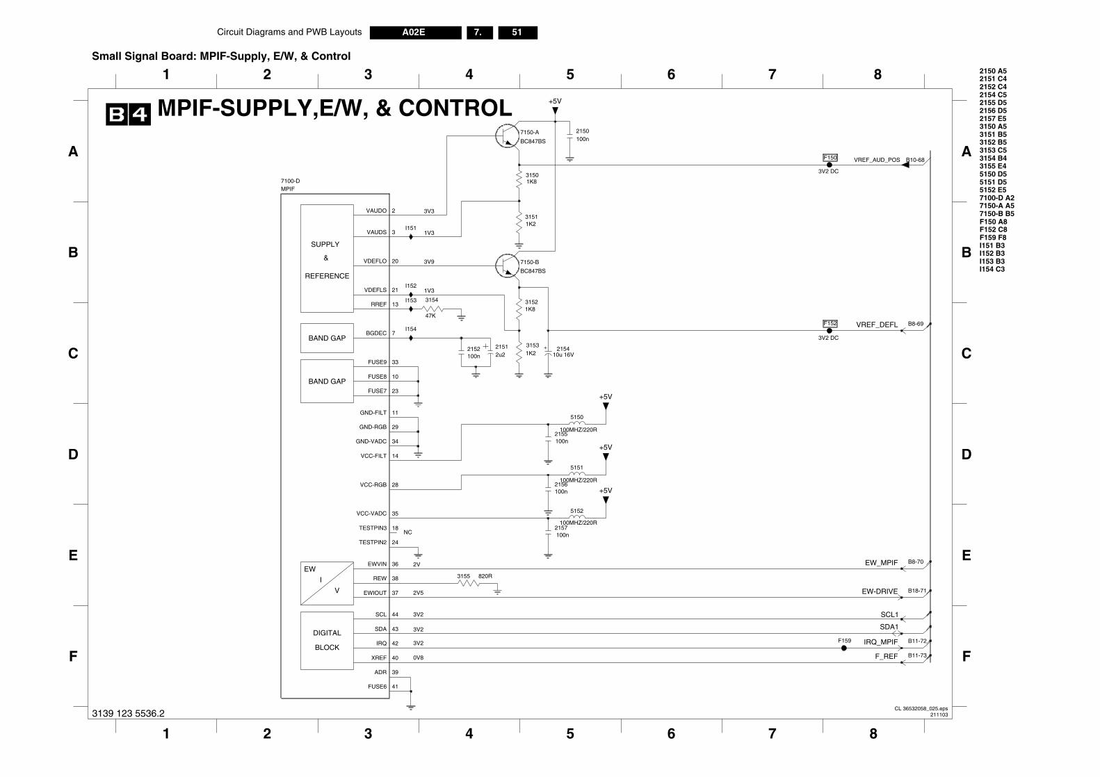
Circuit Diagrams and PWB Layouts 51A02E 7.
8
B10-68
3153 C5
B8-70
7
B8-69
5151 D5
I151 B3
7100-D A2
F159 F8
5150 D5
5152 E5
D
E
F
8
B18-71
I154 C3
7
A3152 B5
3154 B4
I152 B3I153 B3
2155 D5
2150 A5
B11-72
B11-73
B
C
2151 C42152 C42154 C5
7150-B B5F150 A8
7150-A A5
F152 C8
2157 E5
3155 E4
3151 B53150 A5
2156 D5
VREF_AUD_POS
3V2 DC
3V2 DC
F159
F152
F150
VREF_DEFL
EW-DRIVE
EW_MPIF
IRQ_MPIF
F_REF
SCL1
SDA1
CL 36532058_025.eps211103
EW
I
V
DIGITAL
BLOCK
5 6
F
E
21
2V
2V5
3V2
3V2
3V2
0V8
3 4
43SDA
40XREF
39ADR
37EWIOUT
36EWVIN
41FUSE6
42IRQ
38REW
44SCL
820R3155
3139 123 5536.2
Small Signal Board: MPIF-Supply, E/W, & Control
BAND GAP
SUPPLY
&
REFERENCE
BAND GAP
7150-A
BC847BS
I153
100n
100n2156
MPIF-SUPPLY,E/W, & CONTROL
A
2
C
D
NC
5
B
61 3
3V9
1V3
4
100MHZ/220R
100MHZ/220R
100MHZ/220R
5152
+5V
3V3
1V3
5151
215410u 16V
24TESTPIN2
18TESTPIN3
2VAUDO
3VAUDS
14VCC-FILT
28VCC-RGB
35VCC-VADC
20VDEFLO
21VDEFLS
7BGDEC
23FUSE7
10FUSE8
33FUSE9
11GND-FILT
29GND-RGB
34GND-VADC
13RREF
MPIF7100-D
+5V
+5V
2150100n
47K
3154
5150
2155
2152100n
I154
I152
2151
100n2157
2u2
1K23151
1K83152
1K23153
1K83150
BC847BS
7150-B
I151
+5V
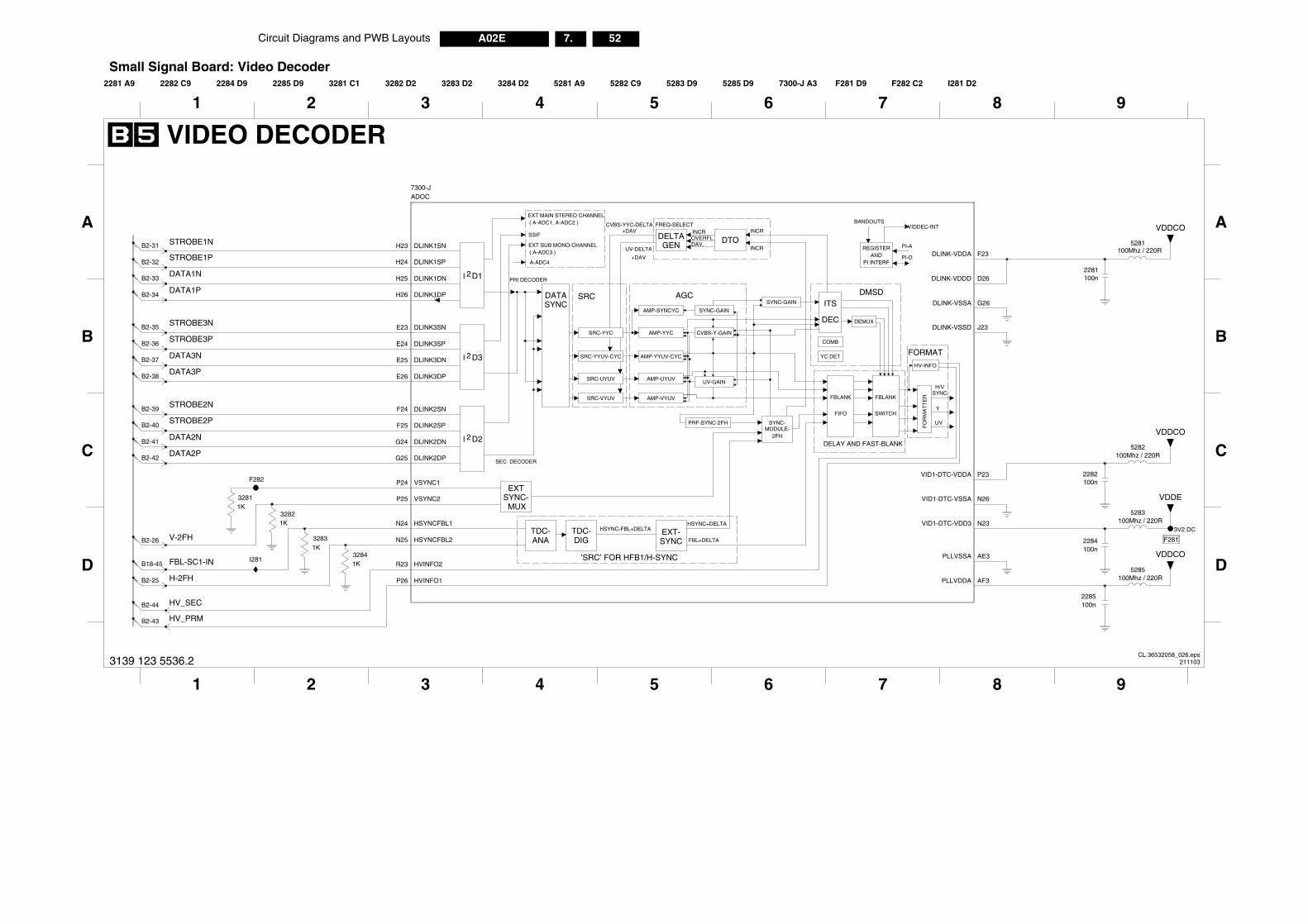
52A02E 7.Circuit Diagrams and PWB Layouts
FO
RM
AT
TE
R
HV-INFO
Y
SYNC
FORMAT
H/V
VIDDEC-INT
PI-A
PI-D
UV
5283100Mhz / 220R
I281 D2
8
C
9
A5281
100Mhz / 220R
D
82 C2
8
100Mhz / 220R
100Mhz / 220R
9
B
AE3PLLVSSA
N23VID1-DTC-VDD3
P23VID1-DTC-VDDA
N26VID1-DTC-VSSA
F281
AF3PLLVDDA
F23DLINK-VDDA
D26DLINK-VDDD
G26DLINK-VSSA
J23DLINK-VSSD
100n2282
100n
VDDCO
2281
5282
VDDCO
VDDCO
5285
100n2285
VDDE
2284100n
CL 36532058_026.eps211103
3V2 DC
21 3 54 6 7
3139 123 5536.2
Small Signal Board: Video Decoder
2I D3
2I D2
( A-ADC1, A-ADC2 )
SSIF
EXT SUB MONO-CHANNEL( A-ADC3 )
A-ADC4
SEC DECODER
TDC-ANA
TDC-DIG
SRC-YYUV-CYC
SRC-UYUV
SRC-VYUV
AMP-YYC
AMP-YYUV-CYC
AMP-UYUV
AMP-VYUV
AMP-SYNCYC SYNC-GAIN
CVBS-Y-GAIN
UV-GAIN
AGC
INCRINCROVERFL.DAV.
INCR
CVBS-YYC-DELTA+DAV
UV-DELTA
+DAV
SYNC-GAIN
PRF-SYNC-2FH SYNC-MODULE-
2FH
EXT-SYNC
HSYNC-FBL+DELTAHSYNC+DELTA
FBL+DELTA
COMB
YC DET
DEMUX
FBLANK
SWITCH
DMSD
REGISTERAND
PI INTERF
BANDOUTSEXT MAIN STEREO CHANNEL
I 2
DATASYNC
PRI DECODER
EXTSYNC-
MUX
SRC-YYC
SRC
DELTAGEN
FREQ-SELECT
DTO
ITS
DEC
FBLANK
FIFO
DELAY AND FAST-BLANK
’SRC’ FOR HFB1/H-SYNC
D1
B
5282 C95281 A93284 D2 5285 D95283 D9
2 3 4 5
B2-44
73282 D2 3283 D2
B2-33
B2-31
B2-35
B2-34
B2-32
C
B2-37
B2-38
1
B2-36
B2-40
B2-39
6
B2-41
B2-26
B18-45
B2-25
VIDEO DECODER
B2-42
3281 C12285 D92284 D9 F2F281 D97300-J A3
B2-43
A
2281 A9 2282 C9
D
P24 VSYNC1
P25 VSYNC2
H26 DLINK1DP
H23 DLINK1SN
H24 DLINK1SP
G24 DLINK2DN
G25 DLINK2DP
F24 DLINK2SN
F25 DLINK2SP
E25 DLINK3DN
E26 DLINK3DP
E23 DLINK3SN
E24 DLINK3SP
N24 HSYNCFBL1
N25 HSYNCFBL2
P26 HVINFO1
R23 HVINFO2
ADOC7300-J
H25 DLINK1DN
32831K
1K3284
F282
1K3281
32821K
I281
HV_SEC
HV_PRM
STROBE1N
STROBE1P
DATA1N
DATA1P
STROBE3N
STROBE3P
DATA3N
DATA3P
STROBE2N
STROBE2P
DATA2N
DATA2P
FBL-SC1-IN
H-2FH
V-2FH
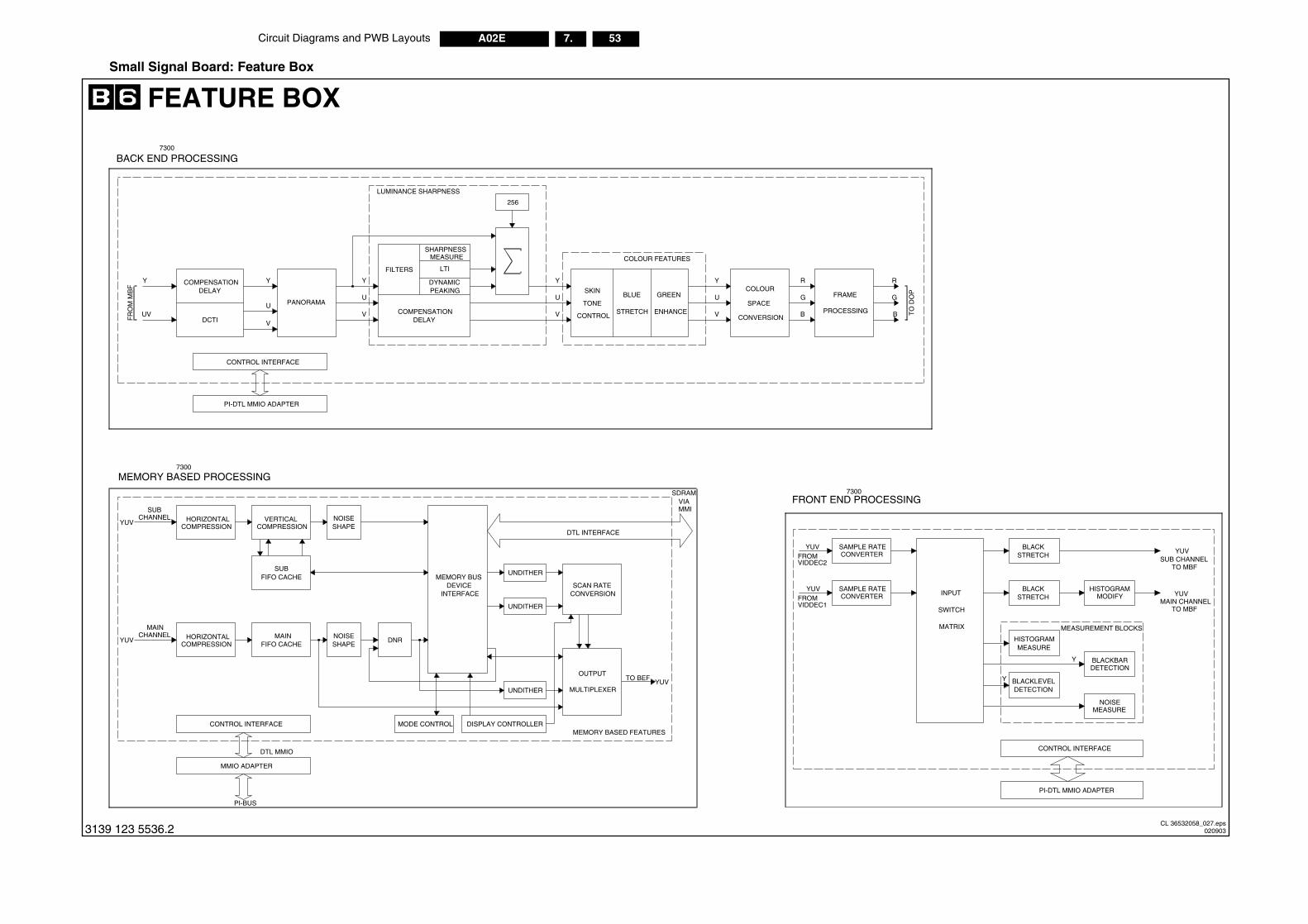
Circuit Diagrams and PWB Layouts 53A02E 7.
MAIN CHANNELTO MBF
CONTROL INTERFACE
PI-DTL MMIO ADAPTER
YUV
YUV
ING
TO
DO
P
BLACKSTRETCH
BLACKSTRETCH
HISTOGRAMMODIFY
HISTOGRAMMEASURE
BLACKLEVELDETECTION
BLACKBARDETECTION
NOISEMEASURE
Y
Y
INPUT
SWITCH
MATRIX MEASUREMENT BLOCKS
SUB CHANNELTO MBF
CL 36532058_027.eps020903
UNDITHER
DISPLAY CONTROLLERMODE CONTROL
OUTPUT
MULTIPLEXER
TO BEFYUV
CONTROL INTERFACE
MMIO ADAPTER
DTL MMIO
PI-BUS
MEMORY BASED FEATURES
3139 123 5536.2
Small Signal Board: Feature Box
YUV
YUV
FRONT END PROCESS
MEMORY BASED PROCESSING
BACK END PROCESSING7300
7300
7300
COLOUR FEATURES
Y
U
V
COLOUR
SPACE
CONVERSION
FRAME
PROCESSING
R
G
B
FR
OM
MB
F
LUMINANCE SHARPNESS
CONTROL INTERFACE
PI-DTL MMIO ADAPTER
SUB
SHAPE
R
G
B
HORIZONTALCOMPRESSION
CHANNELSUB
YUV VERTICALCOMPRESSION
NOISE
FEATURE BOX
COMPENSATION DELAY
DCTI
Y
UV
Y
U
V
PANORAMA
Y
U
V
FILTERS
COMPENSATION DELAY
SHARPNESSMEASURE
DYNAMICPEAKING
LTI
256
Y
U
V
SKIN
TONE
CONTROL
BLUE
STRETCH
GREEN
ENHANCE
FIFO CACHE
HORIZONTALCOMPRESSION
CHANNELMAIN
YUVNOISESHAPE
MAINFIFO CACHE
DNR
MEMORY BUSDEVICE
INTERFACE
UNDITHER
UNDITHER
SCAN RATECONVERSION
DTL INTERFACE
SDRAMVIAMMI
SAMPLE RATECONVERTER
SAMPLE RATECONVERTER
VIDDEC2FROM
VIDDEC1FROM
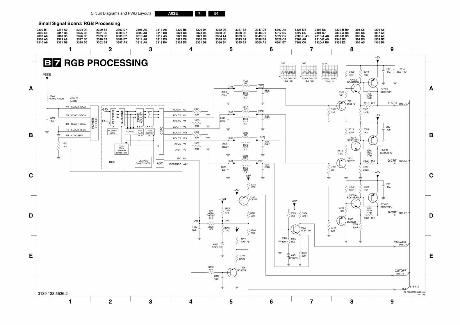
54A02E 7.Circuit Diagrams and PWB Layouts
B18-75
B18-76
B18-77
B18-78
B18-79
B18-112
RES
RES
RES
18R
18R
18R
8 9
8 9
A
B
C
D
E
303 D8304 D7310-A A8310-B A9320-A B8
7320-B B97330-A D87330-B D97346 D57356 E5
I301 C5I302 C6I303 D4I304 D5I305 A5
I306 A6I307 A5I308 A6I309 B5I310 B6
2339100p
7303BC857B
100p2329
2319100p
BC857B7302
7301BC857B
BC847BW7304
3348
3338
3316
3307
1K23318 +8V
16V10u2310
333133R
33R3321
10n2331
232110n
10n2311
100p
7330-ABC847BPN
7320-ABC847BPN
7330-BBC847BPN
7320-BBC847BPN
7310-ABC847BPN
7310-BBC847BPN
4K7
+8V
3332 1K2
33301K2
3333330R
3329330R
+8V
1K23322
3320
330R3323
1K2
+8V
330R3319
3313
3312 1K2
33R
1K23310
330R3311
330R3309
R-CRT
G-CRT
B-CRT
TILT
CUTOFF
Y-SCAVEM
CL 36532058-083.eps211103
I310
200mV / div DC10µs / div
1 2 3 4 5 6 7
E
2305
1u0
33R3306
BAS3166301
1K23305
22K
PDZ-2.7B6327
100n2346
33456K8
820R
3356
BC857B7356
10K3343
3139 123 5536.2
Small Signal Board: RGB Processing
RGBB
LAN
KIN
G
CTRLSCAVEM
FIXEDBEAM
CURRENTSWITCH OFF
CD
AC
RGBGAIN
RGBCUTOFF
LEAKAGECOMPENSATORRGB
PO
WE
RS
OU
RC
E
GFXB
LEN
DE
R
DR
IVE
AD
JUS
T
BLENDER
ADC
RGB PROCESSING
100Mhz / 220R
RESRES
0R
0R
0R
RES
RES
RES
RES
RES
RES
RES
RES
1 2 3 4 5 6 7
A
B
C
D
2300 B12305 E62307 A62308 A52310 A9
2311 A92317 B62318 B52319 A82321 B9
2324 D42325 C52326 C62327 B62328 B5
2329 B82331 C92339 D82346 E53302 B1
3303 D73304 D73305 E73306 E73307 A8
3308 A53309 A83310 A83311 A83312 A8
3313 A83316 B83317 A53318 D53319 B8
3320 B83321 C83322 C83323 C83324 D5
3326 D43328 C53329 C83330 C83331 D8
3332 D83333 D83334 A43335 B43336 B4
3337 B43338 D83339 B53343 E43345 E5
3347 D63348 D63349 C63356 E55300 A1
5307 A55317 B55327 B55328 C56301 E7
6326 D46327 E57300-H A17301 A87302 C8
77777
2307
2327
2317
232682p2325
330R3304
+8V
6K83303
I309 I310
I307 I308
I306
I303
I305
I304
+3V3
I301 I302
6326BAS316
47K3324
+5V
7346BC857B
+8V
22K3347
47K3349
332833R
3339
3317
3308
3335
33R
33R
3334
33R
3336
3337
33R
2328
2318220p
220p
W4 CDAC2-VDDA
Y3 CDAC2-VSSA
V2COUTN
V3GOUTP
N1IBC
AA2IBCRANGE
U2ROUTN
U3ROUTP
Y1SVMN
Y2SVMP
220p2308
ADOC7300-H
W2BOUTN
W3BOUTPU1 CDAC-REF
V1 CDAC1-VDDA
U4 CDAC1-VSSA
2324
53282u2
1K23302
VDDE
100n2300
5300
3326
53272u2
53172u2
2u25307
I308
200mV / div DC10µs / div
I306
200mV / div DC10µs / div
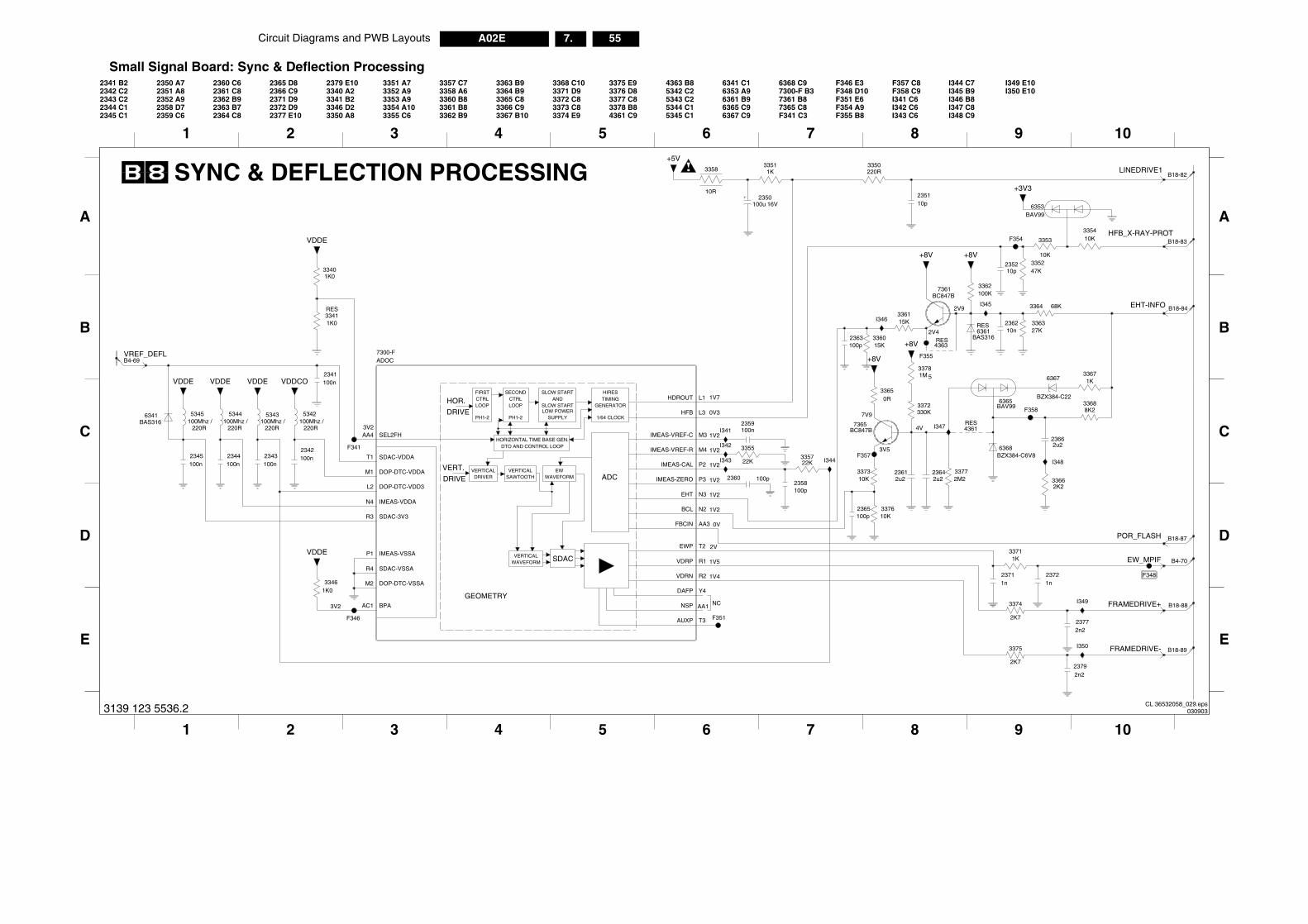
Circuit Diagrams and PWB Layouts 55A02E 7.
+8V
3353
8 9 10
RES
2 C63 C6
I344 C7I350 E10
B18-84
10
B18-83
B18-82
RES
RES
I346 B8I347 C8I348 C9
I349 E10
8 9
I345 B9
D
E
B
A
C
5
1 C658 C957 C8
B4-70
B18-87
B18-89
B18-88
+8V
4V
2V9
2V4
2351
F348
10p
10K
10K3354
23662u2
1K3371
3374
2K7
336327K
3362100K
23792n2
36115K
6361BAS316
23711n
+3V3
2M23377
F358
F355
I347
I348
BAV996353
23721n
3375
2K7
I345
4363
335247K
6368BZX384-C6V8
I350
3372330K
61u2
33781M
33662K2
10n
2u22364
2362
I349
235210p
BAV996365
1K
8K23368
63673367
4361
BZX384-C22
+8V
23772n2
3364 68K
F354
7361BC847B
FRAMEDRIVE+
FRAMEDRIVE-
HFB_X-RAY-PROT
POR_FLASH
EW_MPIF
LINEDRIVE1
EHT-INFO
CL 36532058_029.eps030903
41 2 3 5 6 7
3139 123 5536.2
Small Signal Board: Sync & Deflection Processing
DRIVE
CTRLLOOP
PH1-2
SECONDCTRLLOOP
PH1-2
SLOW STARTAND
SLOW STARTLOW POWER
SUPPLY
HIRESTIMING
GENERATOR
1/64 CLOCK
HORIZONTAL TIME BASE GEN.DTO AND CONTROL LOOP
EWWAVEFORM
VERTICALSAWTOOTH
VERTICALWAVEFORM
VERTICALDRIVER
VERT.
DRIVE
HOR.FIRST
ADC
SDAC
GEOMETRY
22K
5344
2343 C22344 C12345 C1 F341 C3
F346 E3
B
C
D
E
100Mhz /220R
B4-69
2364 C8 3355 C63354 A10
3374 E9
220R 220R
2371 D92372 D92377 E10
2379 E106353 A96361 B96365 C96367 C9
F348 D10F351 E6F354 A9F355 B8
2361 C82362 B92363 B7 I34
I343373 C8
3341 B23346 D23350 A8
2360 C6
3353 A93352 A93351 A7
3340 A23375 E93376 D8
5345 C1
6341 C1
220R
SYNC & DEFLECTION PROCESSING
A
100Mhz /
1 2 3 4 5 6 7
3361 B83362 B9 4361 C9
3378 B83377 C8
0R
5342 C22342 C22341 B2 4363 B8
5343 C25344 C1
3357 C73358 A63360 B8
RES
3363 B93364 B93365 C83366 C9
2366 C93372 C8
100Mhz /
2365 D8
I34F3F3
2359 C6
NC
3367 B10
3368 C103371 D9
7365 C87361 B87300-F B36368 C9
100Mhz /
2350 A72351 A82352 A92358 D7
3V2
3V2
1V7
0V3
1V2
1V2
1V2
1V2
1V2
1V2
0V
2V
1V5
1V4
7V9
3V5F341
BC847B7365
1K03341
F346 F351
F3573355
3
3365
100p2360
2344100n
AA3
HDROUT L1
HFB L3
IMEAS-CAL P2
IMEAS-VDDAN4
IMEAS-VREF-C M3
IMEAS-VREF-R M4
IMEAS-VSSAP1
IMEAS-ZERO P3
NSP AA1
SDAC-3V3R3
SDAC-VDDAT1
SDAC-VSSAR4
SEL2FHAA4
VDRN R2
VDRP R1
7300-FADOC
AUXP T3
BCL N2
BPAAC1
DAFP Y4
DOP-DTC-VDD3L2
DOP-DTC-VDDAM1
DOP-DTC-VSSAM2
EHT N3
EWP T2
FBCIN
336015K
3346
5343
1K0
+5V
2345100n
337610K
VDDE
100p2365
100u2350
16V
VDDE
I343 I344
I342
I346
5345
337310K
5342
232
33401K0
2343100n 22K
3357
BAS3166341
2341100nVDDEVDDE
100n2342
+8V
VDDE
2363100p
3358
10R
1K3350220R
3351
VDDCO
I341
2358100p
100n2359
VREF_DEFL
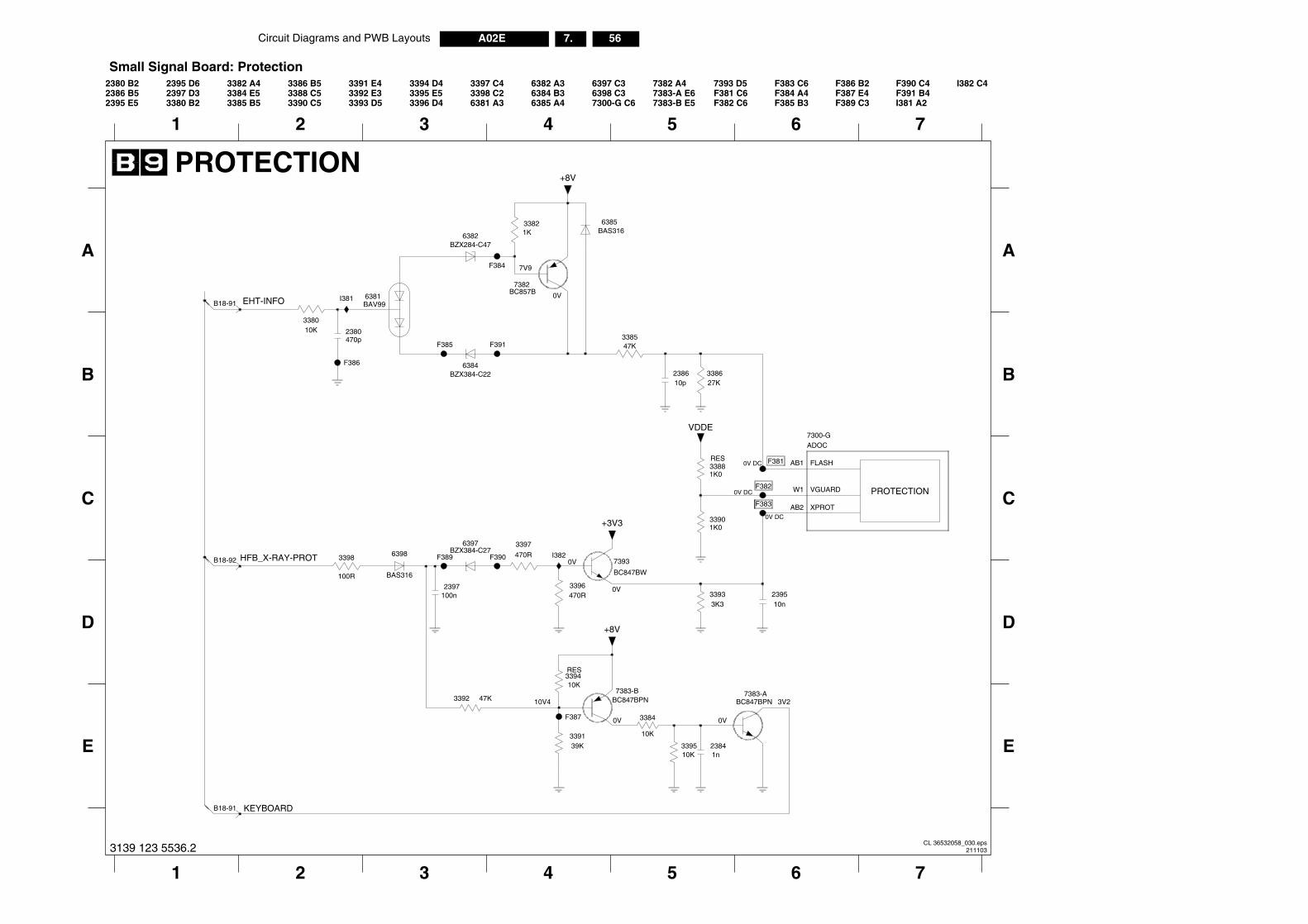
56A02E 7.Circuit Diagrams and PWB Layouts
CTION
I382 C4
E
D
7
C
391 B481 A2
390 C4
B
A
7
CL 36532058_030.eps211103
E
0V
10V4 3V2
RES
B18-91
3 4 5 61 2
0V
7383-BBC847BPN BC847BPN
7383-A
339510K
3392 47K
339139K
3384
10K
10K3394
23841n
F387
KEYBOARD
3139 123 5536.2
Small Signal Board: Protection
PROTE
2397100n
F391
33933K3
I382
1
7393 D5F381 C6F382 C6
F383 C6
3
6382 A36384 B3
7300-G C66398 C3
D
A
F387 E4
B18-91
RES
F384 A4F389 C32395 E5
PROTECTION
2380 B2F
B18-92
I3
F
F385 B3
F386 B22395 D6
3390 C52386 B5
3386 B5
B
C
7383-B E52397 D3
5 6
3397 C4
43380 B2
3382 A43384 E53385 B5
3398 C26381 A3
3388 C53391 E4
6385 A4
6397 C33392 E33393 D5
7382 A47383-A E6
3394 D43395 E53396 D4
2
239510n
7V9
0V
0V DC
0V DC
0V DC
0V
0V
1K03390
F389 F390
BAS316
6398 BZX384-C276397
FLASHAB1
VGUARDW1
XPROTAB2
VDDE
+3V3
7300-GADOC
6381BAV99
F383
7382
338010K
33821K
BC857B
3396470R
7393
BC847BW
3397
470R
+8V
338547K
338627K
33881K0
F382
100R
2380470p
F386
3398
F384
238610p
BAS3166385
6382BZX284-C47
F381
+8V
I381
6384BZX384-C22
HFB_X-RAY-PROT
EHT-INFO
F385
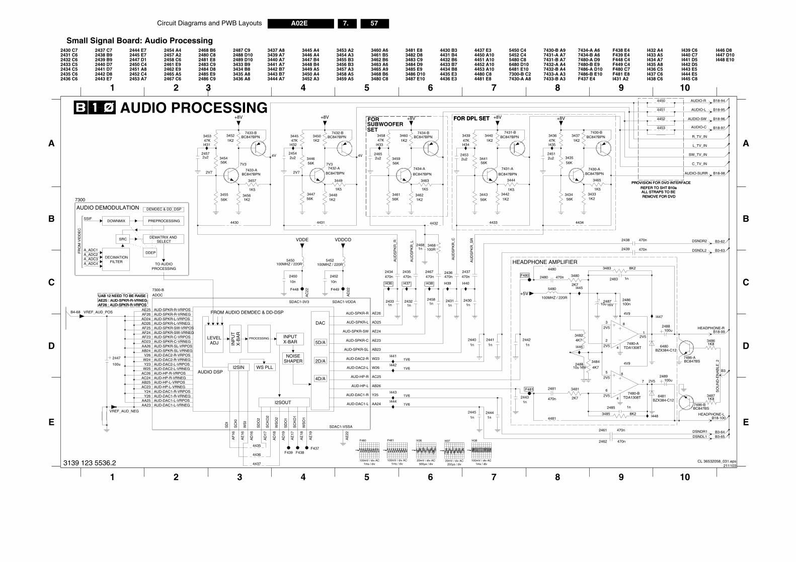
Circuit Diagrams and PWB Layouts 57A02E 7.
8 9 10
PROVISION FOR DVD INTERFACE
REMOVE FOR DVD
A
B
C
D
E
REFER TO SHT B10a
108 9
I437 C6I438 C6
I439 C6I440 C7I441 D5I442 D5I443 E5I444 E5I445 C8
I446 D8I447 D10I448 E10
REMOVE FOR DVDALL STRAPS TO BEREFER TO SHT B10a
B18-100
PROVISION FOR DVD INTERFACE
1K8
B3
4V9
4V9
2V5
2V5
2V5
2V52V5
2V5
ALL STRAPS TO BE
7434-A A67434-B A67480-A D97480-B E97486-A D107486-B E10
MHZ / 220R
B18-95
I433 A5I434 A7I435 A8I436 C5
30-B A931-A A731-B A7
B18-96
B18-98
B18-97
32-A A432-B A433-A A333-B A3
1V6
F437 E4
F438 E4F439 E4F448 C4F449 C4F480 C7F481 E8I431 A2
I432 A4
B3-65
B18-99
B3-64
AMPLIFIER
B18-94
B3-63
B3-62
7486-B
3487
7486-ABC847BS
BC847BS
4453
4452
343556K
343456K
470n
100u2488
I448
2443
2481
470n
8K23485
3481
2K7
4480
4481
I435
1K83486
AUD-DAC1-R-VRNEGAA25 AUD-DAC1-L-VRPOS
Y25AUD-DAC1-RY26
4434
34331K2
7430-ABC847BPN
24512u2
4451
2K7
3480
6480BZX384-C12
TDA1308T7480-A
3
2
1
8
4
4450
2486100n
248710u16V
2462 470n
2461 470n
I447
I445
I446
2439 470n
470n2438
2489100u
BZX384-C126481
3483 8K2
5
6
7
8
4
1n2483
TDA1308T7480-B
5480
34371K2
+8V
343647K
7430-BBC847BPN
3465
1K5
16V10u2484
3484
4K7
2485 1n
4K73482
HEADPHONE-L
SO
UN
D-E
NA
BLE
_2
AUDIO-L
AUDIO-R
AUDIO-SW
DSNDR2
DSNDL2
DSNDR1DSNDL1
AUDIO-C
AUDIO-SURR
C_TV_IN
SW_TV_IN
L_TV_IN
R_TV_IN
HEADPHONE-R
CL 36532058_031.eps211103
I2SOUT
VREF_AUD_NEG
E
1 2 3 4 5 6 7
1V6
F438F437
1n
AE
22
SDAC1-VSSA
AF
16
SD
I
AE
17
SD
O1
AD
17
SD
O2
AD
16
WS
I
AE
19
WS
O1
WS
O2
AD
19
SC
KI
AE
16
AE
18
SC
KO
1
AD
18
SC
KO
2
AUD-DAC1-L AA24AA23 AUD-DAC1-L-VRNEG
F439
1n2444
I444
1n2445
4437
4436
4435
3139 123 5536.2
F480
100mV / div AC1ms / div
F481
100mV / div AC1ms / div
I437
20mV / div AC200µs / div
I438
100mV / div AC1ms / div
I436
20mV / div AC500µs / div
Small Signal Board: Audio Processing
PROCESSING INPUTX-BAR
WS PLL
NOISESHAPER
I2SIN
DAC
5D/A
2D/A
4D/A
FROM AUDIO DEMDEC & DD-DSP
AUDIO DSP
LEVELADJ IN
PU
TX
-BA
R
2u2
344756K
34601K2
5 6 7
FOR DPL SET
2439 B9
D
2430 C72431 C62432 C62433 C52434 C52435 C62436 C6
2437 C72438 B9
21 3 4
2440 D72441 D72442 D82443 E7
2444 E72445 E72447 D12450 C42451 A8
3453 A23454 A33455 B33456 B33457 A33458 A5
2453 A7
2454 A42457 A22458 C6
A
B
C
2452 C42462 E92461 E9
2465 A52467 C6
2468 B62480 C82481 E82483 C9
2V7
UAB 12 NEED TO BE RAISE :AE25 : AUD-SPKR-R-VRNEGAF26 : AUD-SPKR-R-VRPOS
7V3
4V
100MHZ / 220R 100MHZ / 220R
PREPROCESSING
7V3
2V7
4V
4451 A104452 A104453 A104480 C84481 E8
5450 C4
2484 D82485 E92486 C9
2487 C92488 D102489 D103433 B93434 B83435 A8
AE25 : AUD-SPKR-R-VRNEGUAB 12 NEED TO BE RAISE :
3436 A8
3437 A83439 A73440 A73441 A73442 B73443 B73444 A7
3445 A43446 A43447 B43448 B43449 A53450 A43452 A3 3459 A5
3460 A63461 B53462 B63463 A63465 A93468 B63480 C8
3481 E8
100
SRC
3482 D83483 C93484 D93485 E93486 D103487 E10
4430 B34431 B44432 B64433 B74434 B84435 E34436 E3
4437 E34450 A10
PROCESSING
5452 C45480 C86480 D106481 E107300-B C27430-A A8
747474
DDEP
7300
SSIF
A_ADC1
SELECT
B4-68
DECIMATION
AF26 : AUD-SPKR-R-VRPOS
DEMDEC & DD_DSP
A_ADC2
74747474
FORSUBWOOFERSET
1V6
1V6
AUDIO DEMODULATION
DEMATRIX AND
AUDIO PROCESSING
TO AUDIOFILTER
FR
OM
VID
DE
C
HEADPHONE
FOR DPL SET
A_ADC3A_ADC4
DOWNMIX
2454
2437470n
2436470n
3439
2480
7431-BBC847BPN
47K
7432-ABC847BPN
24421n
24411n
100R3468
I438 I439
+8V
34621K2
3463
1K5
I436
I434I432 I433
BC847BPN7433-B
2467470n
+8V
SDAC1-3V3
AD
22
SDAC1-VDDA
2450
10n
AUD-SPKR-C-VRPOS
AD25AUD-SPKR-LAD26 AUD-SPKR-L-VRNEGAD24 AUD-SPKR-L-VRPOS
AE26AUD-SPKR-RAF26 AUD-SPKR-R-VRNEGAE25 AUD-SPKR-R-VRPOS
AB23AUD-SPKR-SLAB24 AUD-SPKR-SL-VRNEGAA26 AUD-SPKR-SL-VRPOS
AE24AUD-SPKR-SWAF24 AUD-SPKR-SW-VRNEGAF25 AUD-SPKR-SW-VRPOS
AC
22
Y24 AUD-DAC1-R-VRPOS
W26AUD-DAC2-LW25 AUD-DAC2-L-VRNEGY23 AUD-DAC2-L-VRPOS
W23AUD-DAC2-RW24 AUD-DAC2-R-VRNEGV26 AUD-DAC2-R-VRPOS
AB26AUD-HP-LAC23 AUD-HP-L-VRNEGAB25 AUD-HP-L-VRPOS
AC25AUD-HP-RAUD-HP-R-VRNEGAC24AC26 AUD-HP-R-VRPOS
AE23AUD-SPKR-CAD23 AUD-SPKR-C-VRNEGAF23
ADOC7300-B
24401n
F448 F449
344356K
7434-A
BC847BPN
1K23442
345956K
+8V
2435470n
10n
2452
24532u2
345656K3455
1K2
345456K
24331n
2434470n
24581n
24572u2
I443
I440
+5V
I437
345847K
34501K2
344656K
7432-BBC847BPN3445
47K
F481
F480
5450 5452
24652u2
BC847BPN7433-A
346156K
344156K
VDDE VDDCO
34401K2
VREF_AUD_POS
3452345347K 1K2
2447
100u I442
I441
4432 4433
7434-BBC847BPN
3449
1K5
34481K2
I431
3457
1K5
4430 4431
24311n
24321n
1n2468
3444
1K5
+8V
BC847BPN
7431-A
24301n
AU
DS
PK
R_R
AU
DS
PK
R_L
AU
DS
PK
R_C
AU
DS
PK
R_S
R
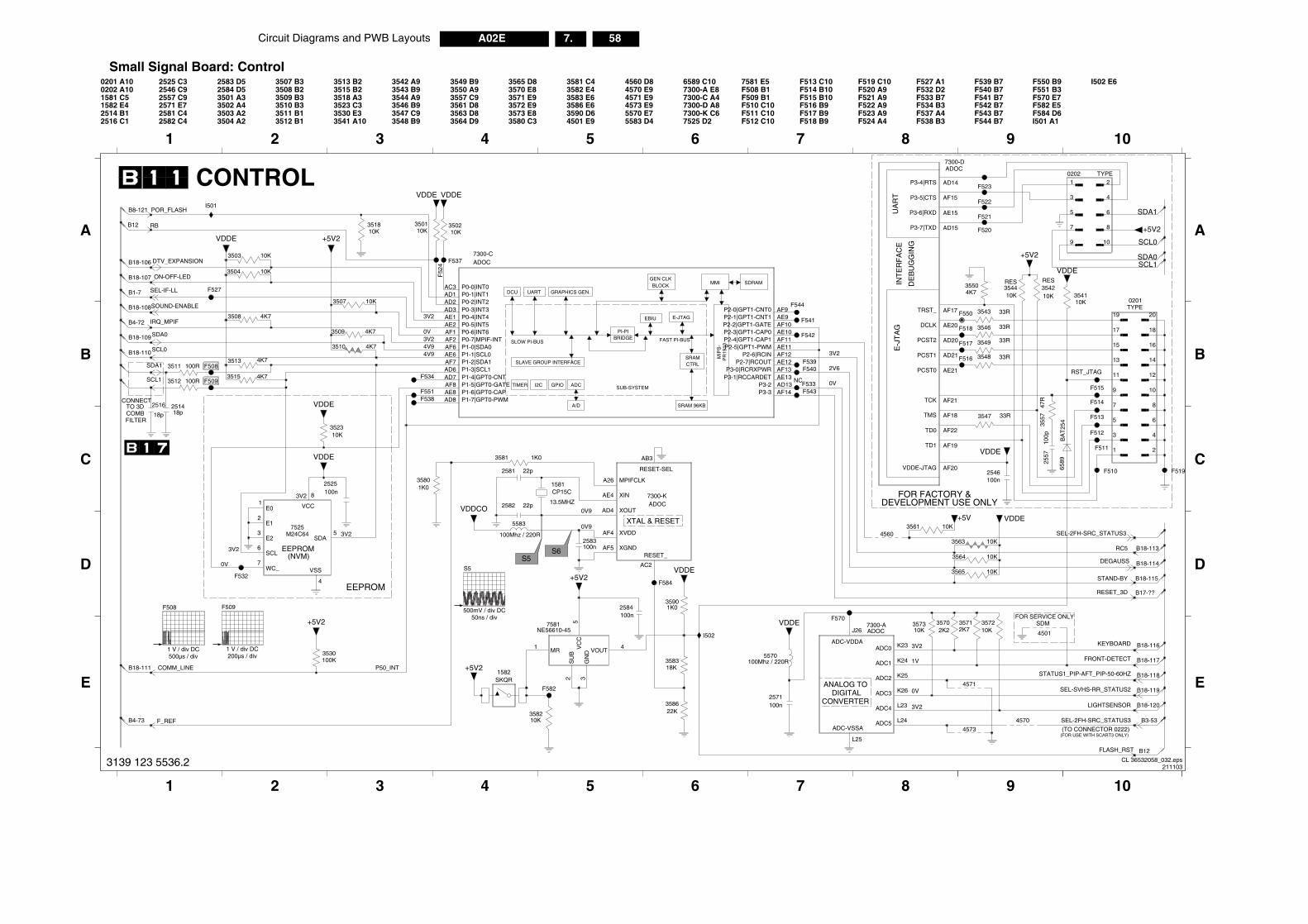
58A02E 7.Circuit Diagrams and PWB Layouts
E-J
TA
G
DE
BU
GG
ING
INT
ER
FA
CE
8
(FOR USE WITH SCART3 ONLY)
RES
E
B18-117
OR FACTORY &ELOPMENT USE ONLY
B18-114
B18-116
RES
F541 B7
B18-118
F540 B7
FOR SERVICE ONLY
F539 B7
F543 B7F542 B7
F532 D2F533 B7
F537 A4F538 B3
F534 B3
F527 A1
B18-119
B17-??
A
B
C
D
8 9 10
9 10
I502 E6
I501 A1
F582 E5F570 E7
F584 D6
F551 B3
3V2
1V
0V
3V2
B12
(TO CONNECTOR 0222)
B18-113
B18-120
F544 B7
F550 B9
B18-115
SDM
B3-53
F511
F523
5570
F519
3563 10K
F550 19
2
20
3 4
5 6
7 8
9
TYPE0201
1
10
11 12
13 14
15 16
17 18
33R3548
F521
4570
4501
F515
3549 33R
F514
+5V2
F513
TD1
AF18TMS
AF17TRST_
AF20VDDE-JTAG
7300-D
AE20DCLK
AD14P3-4|RTS
AF15P3-5|CTS
AE15P3-6|RXD
AD15P3-7|TXD
AE21PCST0
AD21PCST1
AD20PCST2
AF21TCK
AF22TD0
AF19
ADOC
33R3547
F517
F520
3557
47R
23ADC0
24
25
26
23
24
1MR
UB
V 4VOUT
ND
35702K73571
2K2
33R
10K
3543
F512
3544
+5V
3565 10K
VDDE
33R3546
10K3573
4573
10K
+5V2
10K3542
3541
F518
10K3564
BA
T25
465
89
100n2546
10
2
3 4
5 6
7 8
9
0202 TYPE1
4K73550
10K3561
3530
10K3572
4571
VDDE
VDDE
F510
F516
2557
100p
F522
SEL-2FH-SRC_STATUS3
DEGAUSS
RESET_3D
SCL0
SDA1
SCL1SDA0
FRONT-DETECT
STAND-BY
RST_JTAG
FLASH_RST
STATUS1_PIP-AFT_PIP-50-60HZ
SEL-SVHS-RR_STATUS2
SEL-2FH-SRC_STATUS3
RC5
LIGHTSENSOR
KEYBOARD
CL 36532058_032.eps211103
1 V / div DC200µs / div
1 V / div DC500µs / div
ANALOG TODIGITAL
CONVERTER
P50_INT
E
1 2 3 4 5 6
B4-73
7
B18-111100Mhz / 220R
F5822571100n
SKQR1582
22K3586
10K3582
L25
ADC-VSSA
KADC1
KADC2
KADC3
LADC4
LADC5
2S
3G
+5V2358318K
100KCOMM_LINE
F_REF
3139 123 5536.2
Small Signal Board: Control
XTAL & RESET
UA
RT
SLOW PI-BUS
A/D
PI-PIBRIDGE
MIP
S-
FAST PI-BUS
SRAMCTRL
SRAM 96KB
SUB-SYSTEM
PR
1910
GEN CLKBLOCK
MMI SDRAM
DCU
EBIU E-JTAG
UART GRAPHICS GEN.
SLAVE GROUP INTERFACE
TIMER I2C GPIO ADC
F538
35801K0
F544
3503 10K
3504
3504 A2
0201 A10 3507 B3
CONNECT
EEPROM
2516 C1
2525 C3
(NVM)
FDEV13.5MHZ
COMB
EEPROM
100Mhz / 220R
B18-109
M24C64
4570 E94571 E9
F524 A4
NC
F512 C10
F513 C103570 E83571 E93572 E93573 E83580 C3
3581 C43582 E43583 E63586 E63590 D6
A
B
C
D
3515 B23518 A3
7
3550 A93557 C9 F509 B1
F510 C10F511 C10
CONTROL
F514 B10F515 B10F516 B9F517 B9F518 B9
F519 C10F520 A9F521 A9F522 A9F523 A9
3V2
3V20V
4V94V9
3V2
3V2
3V2
0V
0V9
0V9
3V2
2V6
0V
6
B18-107
B1-7
1 2 3 4 5
7300-D A8
TO 3D
F508 B1
FILTER
B8-121
7300-C A47300-A E8
7581 E56589 C10
4573 E95570 E75583 D4
3561 D8
B18-110
B18-108
7525 D2
3510 B33511 B13512 B1
3513 B2
7300-K C63563 D83523 C33530 E33541 A10
3542 A93543 B93544 A93546 B93547 C93548 B9
3549 B9
B12
B4-72
B18-106
0202 A101581 C51582 E42514 B1
3564 D9
3565 D82546 C92557 C92571 E72581 C42582 C4
2583 D52584 D53501 A33502 A43503 A2
4501 E9
4560 D83508 B23509 B3
10K
VDDE
F534
3501
F52
4
3507 10K
4K73508
F551F533
3515 4K7
VDDCO
2581 22p
3509 4K7
CP15C1581
F508
100n2584
S5S6
18p
2516
3510 4K7
F532
F542
F541
F540
VDDE
VDDE
5583
3590
F509
1K0
2582 22p
VDDE
251418p
3581 1K0
I501
I502
VDDEVDDE
+5V2
3512 100R
4K73513
J26
ADC-VDDAK
5C
C
ADOC7300-A
NE56610-457581
+5V2
P3-3
AD7 P1-4|GPT0-CNTAF8 P1-5|GPT0-GATEAE8 P1-6|GPT0-CAPAD8 P1-7|GPT0-PWM
AF9P2-0|GPT1-CNT0AE9P2-1|GPT1-CNT1AF10P2-2|GPT1-GATEAE10P2-3|GPT1-CAP0AF11P2-4|GPT1-CAP1AE11P2-5|GPT1-PWMAF12P2-6|RCINAE12P2-7|RCOUTAF13P3-0|RCRXPWRAE13P3-1|RCCARDETAD13P3-2AF14
AC3 P0-0|INT0AD1 P0-1|INT1AD2 P0-2|INT2AD3 P0-3|INT3AE1 P0-4|INT4AE2 P0-5|INT5AF1 P0-6|INT6AF2 P0-7|MPIF-INTAF6 P1-0|SDA0AE6 P1-1|SCL0AF7 P1-2|SDA1AD6 P1-3|SCL1
ADOC7300-C
10K3518
100n2583
F584
VDDE
F543
F527
+5V2
F537
10K3502
F570
2525100n
4560
A26 MPIFCLK
AB3
RESET-SEL
AC2
RESET_AF5 XGND
AE4 XIN
AD4 XOUT
AF4 XVDD
F5393511 100R
ADOC7300-K
10K
352310K
E01
E12
E23
SCL6
SDA5
VCC
8
VSS
4
WC_7
7525
SDA1
SCL1
RB
DTV_EXPANSION
ON-OFF-LED
SOUND-ENABLE
IRQ_MPIF
SCL0
SDA0
SEL-IF-LL
POR_FLASH
S5
500mV / div DC50ns / div
F509F508
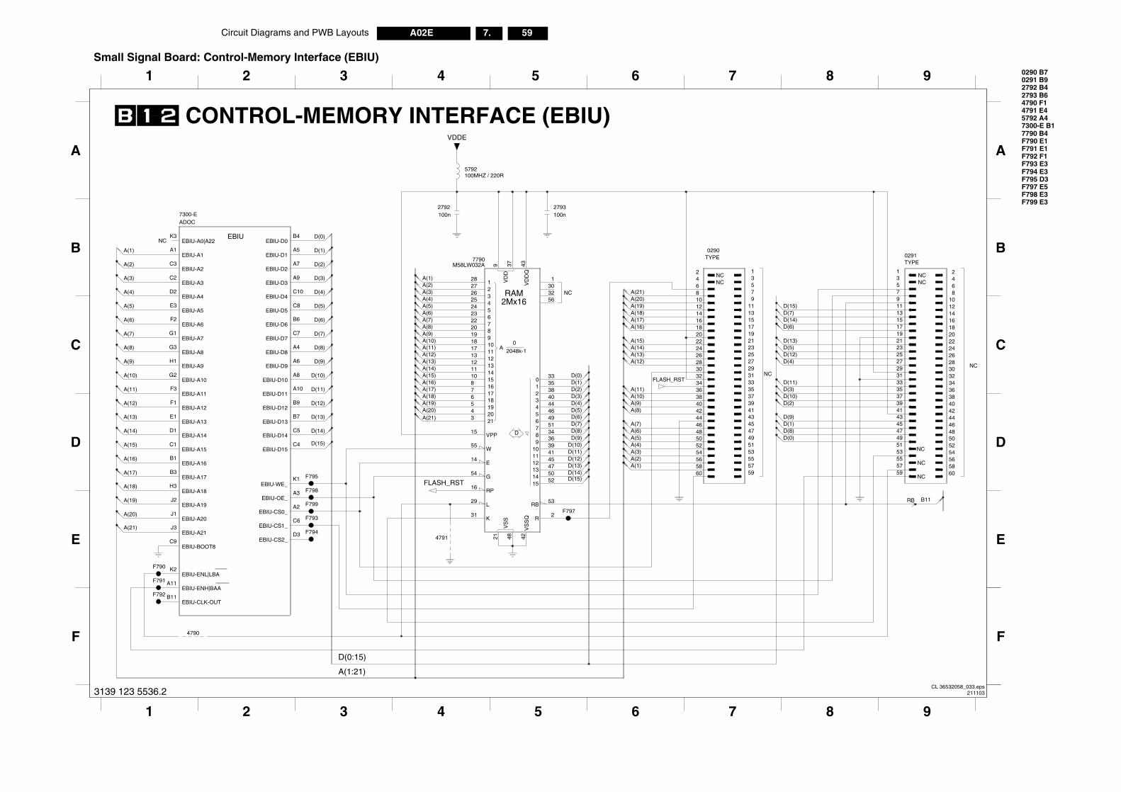
Circuit Diagrams and PWB Layouts 59A02E 7.
NC
NC
B11
NC
F799 E3
NC
F793 E3
B
4790 F1
2792 B42793 B6
0290 B7
9
0291 B9
5792 A44791 E4
F792 F1
NC
A
F795 D3
NC
C
D
E
F
F798 E3F797 E5
F794 E3
7790 B4F790 E1
7300-E B1
F791 E1
8 9
8
5859
6
60
7 89
4647 4849
5
5051 5253 5455 5657
3435 3637 3839
4
4041 4243 4445
2223 2425 2627 2829
3
3031 3233
11 1213 1415 1617 1819
2
2021
0291TYPE
1
10D(15)D(7)D(14)D(6)
D(13)D(5)D(12)D(4)
D(11)D(3)D(10)D(2)
D(9)D(1)D(8)D(0)
RB
CL 36532058_033.eps211103
A(1:21)
FD(0:15)
1 2 3 4 5 6 7
F792
F791
F790
EBIU-ENH|BAAA11
EBIU-ENL|LBAK2
EBIU-CLK-OUTB11
4790
3139 123 5536.2
Small Signal Board: Control-Memory Interface (EBIU)
EBIU
W
VPP
VD
DQ
VS
SQ
VD
D
R
RBV
SS
1918
15
12345678D
0
91011121314
34
1
E
G
RP
0
2
1716151413
2048k-1121110987
5
A
6
L
K
2021
F794
3 5
NC
CONTROL-MEMORY INTERFACE (EBIU)
NC
NC
100MHZ / 220R
A
B
NC
721
NC
4 6
C
D
E
F799
F798
F793
B7
EBIU-D14C5
EBIU-D15C4
EBIU-D2A7
EBIU-D3A9
EBIU-D4C10
EBIU-D5C8
EBIU-D6B6
EBIU-D7C7
EBIU-D8A4
EBIU-D9A6
EBIU-OE_A3
EBIU-WE_K1
EBIU-A5E3
EBIU-A6F2
EBIU-A7G1
EBIU-A8G3
EBIU-A9H1
EBIU-BOOT8C9
EBIU-CS0_A2
EBIU-CS1_C6
EBIU-CS2_D3
EBIU-D0B4
EBIU-D1A5
EBIU-D10A8
EBIU-D11A10
EBIU-D12B9
EBIU-D13
EBIU-A1A1
EBIU-A10G2
EBIU-A11F3
EBIU-A12F1
EBIU-A13E1
EBIU-A14D1
EBIU-A15C1
EBIU-A16B1
EBIU-A17B3
EBIU-A18H3
EBIU-A19J2
EBIU-A2C3
EBIU-A20J1
EBIU-A21J3
EBIU-A3C2
EBIU-A4D2
7300-EADOC
EBIU-A0|A22K3
5792
59
6
60
789
2793100n
474849
5
505152535455565758
3536373839
4
40414243444546
23242526272829
3
3031323334
1213141516171819
2
202122
0290TYPE
1
1011
F797
2792100n
VDDE
F795
4791
9 37 43
15
21 48 42
55
31
29
1303256
2
53
1652
3840444649513436
14
54
222019
3335
3941454750
8765
27
43
26252423
2Mx16
28
181713121110
RAM
M58LW032A7790
A(2)
A(12)
A(10)A(11)
A(1)
A(13)
FLASH_RST
A(14)A(15)
A(16)A(17)A(18)A(19)A(20)A(21)
A(3)A(4)
D(6)D(7)D(8)D(9)
D(10)D(11)D(12)D(13)D(14)
A(20)
D(15)
A(21)
D(15)
A(21)
FLASH_RST
A(5)A(6)A(7)
A(8)A(9)
A(11)A(12)A(13)A(14)A(15)
A(17)A(18)A(19)A(20)
A(16)
D(0)
D(1)
D(2)
D(3)
D(4)
D(5)
D(6)
D(7)
D(8)
D(9)
D(10)
D(11)
D(12)
D(13)
D(14)
D(0)D(1)D(2)D(3)D(4)D(5)
A(1)
A(2)
A(3)
A(4)
A(5)
A(6)
A(7)
A(8)
A(9)
A(10)
A(11)
A(12)
A(13)
A(14)
A(16)
A(17)
A(18)
A(19)
A(15)
A(1)A(2)A(3)A(4)A(5)A(6)A(7)A(8)A(9)A(10)
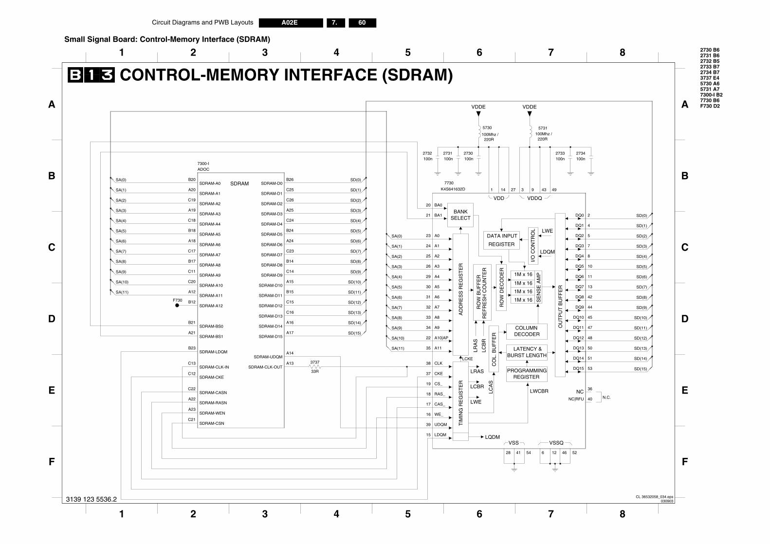
60A02E 7.Circuit Diagrams and PWB Layouts
6
6
6
6
OU
TP
UT
BU
FF
ER
VSSQ
ER
NC
NGTHCY &
DERMN
LWCBR
AS
LDQM
LWE
I/O C
ON
TR
OL
SE
NS
E A
MP
DDQ
TERMMING
LCBR
2733100n
F730 D27730 B6
N.C.
2734 B73737 E45730 A65731 A7
B
C
D
E
F
2730 B62731 B62732 B5
7 8
7300-I B2
A
220R
72733 B7
8
100Mhz /
100n2734
52
9 43 49
6 12 46
47
DQ12 48
DQ13 50
DQ14 51
DQ15 53
5DQ2
7DQ3
8DQ4
10DQ5
11DQ6
13DQ7
DQ8 42
DQ9 44
36
NC|RFU 40
CS_19
2DQ0
4DQ1
DQ10 45
DQ11
DE
5731
SD(0)
SD(1)
SD(2)
SD(3)
SD(4)
SD(5)
SD(6)
SD(7)
SD(8)
SD(9)
SD(10)
SD(11)
SD(12)
SD(13)
SD(14)
SD(15)
CL 36532058_034.eps030903
VSS
TIM
ING
RE
GIS
T
LC
LWE
LQDM
F
E
61 4 532
16 WE_
RAS_
39 UDQM
28 41 54
LDQM15
18
17 CAS_SDRAM-RASN
A23SDRAM-WEN
A22
C22SDRAM-CASN
C21SDRAM-CSN
3139 123 5536.2
Small Signal Board: Control-Memory Interface (SDRAM)
1M x 1
1M x 1
1M x 1
1M x 1
BANKSELECT
AD
DR
ES
S R
EG
IST
ER
LCKEBURST LE
LATEN
DECOCOLU
REGISTER
CO
L. B
UF
FE
R
RO
W D
EC
OD
ER
RE
FR
ES
H C
OU
NT
ER
RO
W B
UF
FE
RLR
AS
VDD V
LCB
R
DATA INPUT
REGISPROGRALRAS
SDRAM
A
1 3 4 52
CONTROL-MEMORY INTERFACE (SDRAM)
6
B
C
D
100Mhz /220R
2731100n
5730
2732
VDDE
100n
3737
33R
1 14 27 3
26
A429
A530
A631
A732
A833
A934
20 BA0
BA121
CKE37
CLK38
A14SDRAM-UDQM
7730
K4S641632D
A023
A124
22 A10|AP
A1135
A225
A3
SDRAM-D10
B15SDRAM-D11
C15SDRAM-D12
C16SDRAM-D13
A16SDRAM-D14
A17SDRAM-D15
C26SDRAM-D2
A25SDRAM-D3
C24SDRAM-D4
B24SDRAM-D5
A24SDRAM-D6
C23SDRAM-D7
B14SDRAM-D8
C14SDRAM-D9
B23SDRAM-LDQM
SDRAM-A3
C18SDRAM-A4
B18SDRAM-A5
A18SDRAM-A6
C17SDRAM-A7
B17SDRAM-A8
C11SDRAM-A9
B21SDRAM-BS0
A21SDRAM-BS1
C12SDRAM-CKE
C13SDRAM-CLK-IN
A13SDRAM-CLK-OUT
B26SDRAM-D0
C25SDRAM-D1
A15
ADOC7300-I
B20SDRAM-A0
A20SDRAM-A1
C20SDRAM-A10
A12SDRAM-A11
B12SDRAM-A12
C19SDRAM-A2
A19
VD
2730
F730
100n
SD(11)
SD(10)
SD(9)
SD(8)
SD(7)
SD(6)
SD(5)
SD(4)
SD(3)
SD(2)
SD(1)
SD(0)
SA(11)
SA(10)
SA(9)
SA(8)
SA(7)
SA(6)
SA(5)
SA(4)
SA(3)
SA(2)
SA(1)
SA(0)
SA(0)
SA(1)
SA(2)
SA(3)
SA(4)
SA(5)
SA(6)
SA(7)
SA(8)
SA(9)
SA(10)
SA(11)
SD(15)
SD(14)
SD(13)
SD(12)

Circuit Diagrams and PWB Layouts 61A02E 7.
2601
100n
2607
100n2609
9 108
1098
A
B
C
D
2615100n 100n
26002611100n
2604
100n
100n2612 10
0n
2618100n00n
620
B10
VS
SE
6
B8
VS
SE
7
B5
VS
SE
8
B2
VS
SE
9
B16
VS
SE
4
B13
VS
SE
5
B19
VS
SE
3
E2
VS
SE
10
H2
VS
SE
11
T4
VS
SE
12
AE
7V
SS
E13
AD
11V
SS
E14
AE
14V
SS
E15
AC
20V
SS
E16
AC
21V
SS
E17
V24
VS
SE
18
T26
VS
SE
19
B22
VS
SE
2
D8
VD
DE
7
D5
VD
DE
8
D4
VD
DE
9
B25
VS
SE
1
H4
VD
DE
11
AC
4V
DD
E12
AC
5V
DD
E13
AC
6V
DD
E14
AC
11V
DD
E15
AC
17V
DD
E16
AC
18V
DD
E17
AC
19V
DD
E18
V23
VD
DE
19
U26
VD
DE
20
J25
VD
DE
21
D19
VD
DE
3
D16
VD
DE
4
D13
VD
DE
5
D10
VD
DE
6
E4
VD
DE
10
CL 36532058_035.eps030903
Small Signal Board: ADOC Supply
SUPPLY
NC
NC
VDDE
+1V830R
5600
7300-L B65600 C12649 C2 5601 D7 7300-M A1
RES
F601 C12629 C6
100Mhz /
2628 C72612 C92615 C8
2618 C82620 C8
2644 D72645 C1
A
NCNC
I601 D8
4 5 6 7
2600 C102601 C10
2604 C10
2 3
2611 C9
1 2 3 4
2622 C7 2630 C62633 C6
2634 C62638 C22607 C9
2609 C9
100Mhz/
1
5 6
2623 C7
7
C
B
ADOC SUPPLY
D
2633100n100n
2634 2622100n
100n
2623
2629
100n
100n2630
2628
100n
VDDCO
264510u 16V
+3V3
100u2649
F601
264422u 16V
100n2638 1
2
L4
U24
U23
T25
T24
T23
P4
V4
F26
G23
R24
R25 V25
U25
D7
VS
SIS
18
K4
VS
SIS
2
AD
5V
SS
IS3
AE
5V
SS
IS4
AC
7V
SS
IS5
AD
9V
SS
IS6
AD
10V
SS
IS7
AD
12V
SS
IS8
AC
15V
SS
IS9
ADOC7300-M T
14V
SS
E54
T15
VS
SE
55
T16
VS
SE
56
G4
VS
SIS
1
M24
VS
SIS
10
M25
VS
SIS
11
L26
VS
SIS
12
D23
VS
SIS
13
D20
VS
SIS
14
D18
VS
SIS
15
D14
VS
SIS
16
D12
VS
SIS
17
P12
VS
SE
40
P13
VS
SE
41
P14
VS
SE
42
P15
VS
SE
43
P16
VS
SE
44
R11
VS
SE
45
R12
VS
SE
46
R13
VS
SE
47
R14
VS
SE
48
R15
VS
SE
49
R16
VS
SE
50
T11
VS
SE
51
T12
VS
SE
52
T13
VS
SE
53
L15
VS
SE
25
L16
VS
SE
26
M11
VS
SE
27
M12
VS
SE
28
M13
VS
SE
29
M14
VS
SE
30
M15
VS
SE
31
M16
VS
SE
32
N11
VS
SE
33
N12
VS
SE
34
N13
VS
SE
35
N14
VS
SE
36
N15
VS
SE
37
N16
VS
SE
38
P11
VS
SE
39
J24
VS
SE
20
L11
VS
SE
21
L12
VS
SE
22
L13
VS
SE
23
L14
VS
SE
24
J4V
DD
I1
D15
VD
DI1
0
D11
VD
DI1
1
D9
VD
DI1
2
AB
4V
DD
I2
AC
9V
DD
I3
AC
12V
DD
I4
AC
14V
DD
I5
R26
VD
DI6
M23
VD
DI7
D24
VD
DI8
D21
VD
DI9
D22
VD
DE
2
ADOC7300-L
F4
VD
DC
O1
AC
8V
DD
CO
2
AC
10V
DD
CO
3
AC
13V
DD
CO
4
AC
16V
DD
CO
5
M26
VD
DC
O6
D17
VD
DC
O7
D6
VD
DC
O8
D25
VD
DE
1
560130R
I601
3139 123 5536.2
1V8 DC
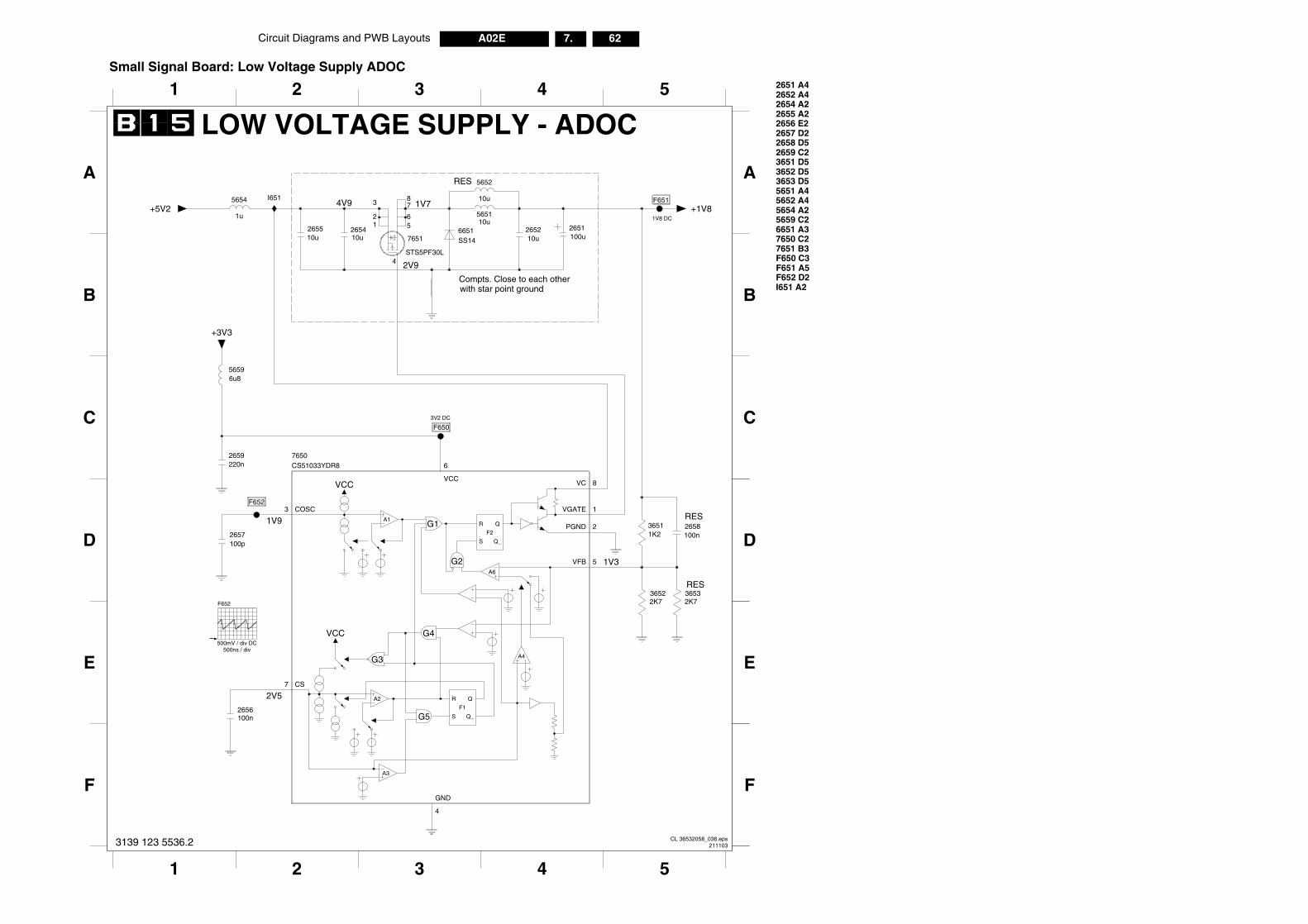
62A02E 7.Circuit Diagrams and PWB Layouts
A4500ns / div
G3
G5
A2
A3
F1
Q_
QR
S
1 2
F
E
F
2V5
E
3 4 5
100n2656
7 CS
GND
4
CL 36532058_036.eps2111033139 123 5536.2
Small Signal Board: Low Voltage Supply ADOC
R
S
Q
Q_
F2
VCC
G2
G4
A1
A6
G1
VCC
+1V81u
5654
RES
RES
F652 D2
RES
5
with star point groundCompts. Close to each other
LOW VOLTAGE SUPPLY - ADOC
I651 A2
A
B
6651 A35659 C2
C
D
2651 A41 2
5652 A4
7650 C27651 B3
2657 D2
2655 A22656 E2
F651 A5F650 C3
2652 A42654 A2
4V9 1V7
2V9
1V9
1V3
2658 D5
A
B
C
D
3 4
3651 D53652 D53653 D55651 A4
2659 C2
5654 A210u5651
265510u
36511K2
5652
10u
+5V2
100n2658
+3V3
2K73652
6u85659
220n2659
100p2657
100u2651
SS146651
10u2652
I651
F652
F650
F651
36532K7
12
3
10u2654
VGATE 1
7651
STS5PF30L
56
78
4
CS51033YDR87650
COSC3
PGND 2
VC 8VCC
6
VFB 5
1V8 DC
F652
500mV / div DC
3V2 DC
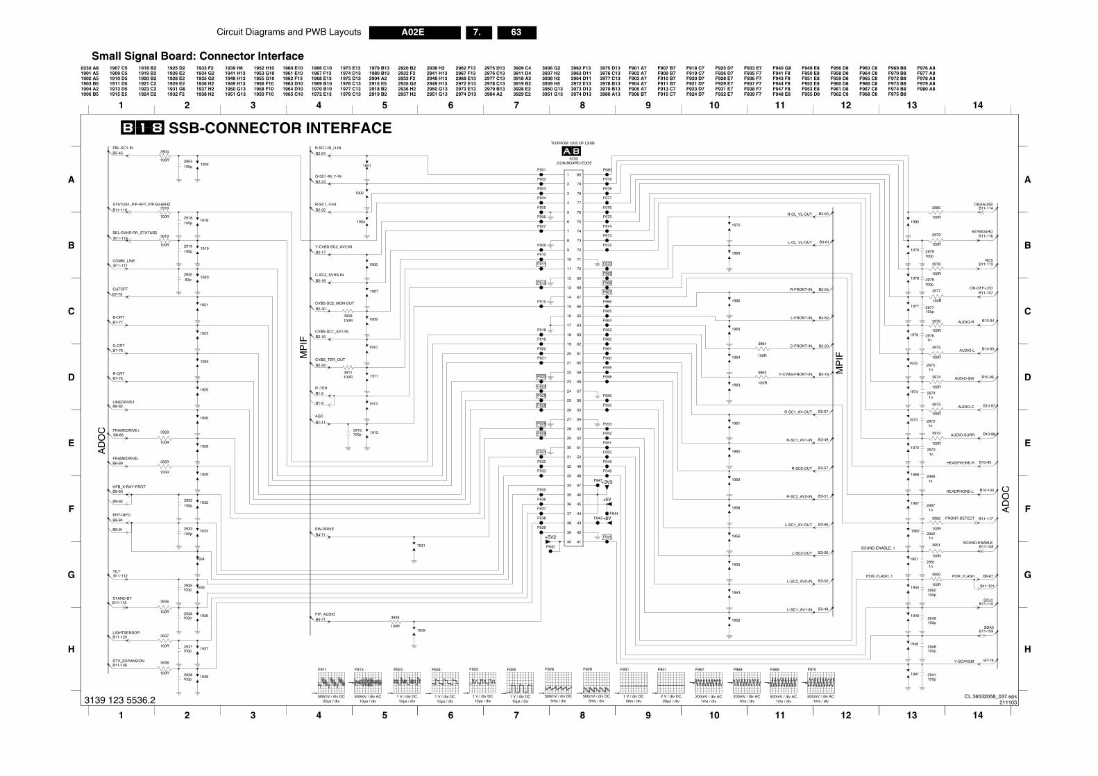
Circuit Diagrams and PWB Layouts 63A02E 7.
1975
ON-OFF-LED
RC5
KEYBOARD
DEGAUSS
B11-116
F941 F8F943 F8F944 F8F947 F8F948 E8
F949 E8F950 E8F951 E8
B10-100
B8-87
C
B3-66
B3-61
B3-54
B3-52
B3-51
B3-57
B10-99
F7 F965 C8
B10-98
B10-97
B10-96
F966 C8F960 D8
F962 C8
F964 C8F963 C8
B11-113
F955 D8
F956 D8F958 D8F959 D8
F961 D8
B3-67
F7 F7 F7
F940 G8
B2-19
B2-20
F952 E8F953 E8
B11-107
B10-95
B3-50
B3-56
B
AD
OC
B11-121
B3-49
F7 E7
F967 C8F968 C8
B3-60
B11-114
MP
IF
14
B3-48
B10-94
11 12 13
F978 A8F977 A8F976 A8F969 B8
F970 B8
F979 A8F980 A8
F972 B8F973 B8F974 B8F975 B8
B11-108
B11-117
B7-78
B11-109
F
G
H
B11-110
1972
11 12 13 14
D
E
A
3972
100R
1n2972
1973
2950100p
1950
100R
3980
1980
3962
100R
3975
100R
29751n
100R
3976
1n2976
1978
3979
100R
2949100p
100R
3963
2978100p
29511n
1962
3978
100R
1n2968
1941
3951
100R
1n2962
1974
1949
100R
3974
1948
1n
19672967
1968
100R
3973
1n2974
1951
2977100p
1n2973
2948100p
100R
3950
1979
1931
3964
100R
100p2979
1977
100p2941
F940
1976
3977
100R
Y-CVBS-FRONT-IN
R-SC1_AV1-IN
R-SC2-OUT
R-SC2_AV2-IN
L-SC1_AV-OUT
L-SC2-OUT
L-SC2_AV2-IN
L-SC1_AV1-IN
SOUND-ENABLE_1SOUND-ENABLE
POR_FLASH_1 POR_FLASH
SCL0
SDA0
Y-SCAVEM
AUDIO-L
AUDIO-SW
AUDIO-C
AUDIO-SURR
R-CL_VL-OUT
L-CL_VL-OUT
HEADPHONE-R
HEADPHONE-L
R-FRONT-IN
L-FRONT-IN
C-FRONT-IN
FRONT-DETECT
R-SC1_AV-OUT
AUDIO-R
CL 36532058_037.eps211103
F969
500mV / div AC1ms / div
AC
F970
500mV / div AC1ms / div
PIP_AUDIOB4-71
B11-115
9
G
HB11-106
5 6 7 8 10
B11-120
B11-112
3 41 2
1934
1936
1937
1953
1938
2935100p
1952
100p2938
1939
2937100p
100R
3939
1935
3936
100R
100R
3938
1955
3937
100R
100p2936
TILT
STAND-BY
LIGHTSENSOR
DTV_EXPANSION
3139 123 5536.2
F911
500mV / div DC20µs / div
F913
500mV / div AC10µs / div
F967
200mV / div AC1ms / div
F941
2 V / div DC20µs / div
F931
1 V / div DC5ms / div
F929
500mV / div DC5ms / div
F928
500mV / div DC5ms / div
F926
1 V / div DC10µs / div
F925
1 V / div DC10µs / div
F968
200mV / div 1ms / div
F923
1 V / div DC10µs / div
F924
1 V / div DC10µs / div
Small Signal Board: Connector Interface
1920
2951 G132950 G13
2968 E13
2962 F132967 F13
2972 E13
2937 H2
2938 H22941 H132948 H131955 G10
TO/FROM 1205 OF LSSB
1906 B5
1903 B5
10
B7-79
1907 C5
8 9
1909 C51902 A5
B2-24
4 5 6 7
1962 F131953 G10
1958 F101959 F10
1961 E101918 B2
1956 F10
1960 E10
2935 G22936 H21950 G13
1951 G13
1952 H10
2915 E52918 B22919 B2
2904 A2
2973 E13
F902 A7F903 A7F904 A7F905 A7F906 B7
F907 B7F909 B7F910 B7
3911 D43918 A2
1974 D131975 D131976 C131977 C131931 G6
1979 B131980 B13
MP
IF
B8-83
1921 C2
1924 D2
B11-118
1919 B21920 B2
1923 C2
1925 D2 2920 B22932 F22933 F21948 H13
1949 H131910 D51911 D51913 D51915 E5
3
F936
SSB-CONNECTOR INTERFACEB5-45
B8-89
3975 D13
F937F938F939
F901 A7
3980 A133979 B13
3977 C133978 B13
3976 C133964 D113972 E133973 D133974 D13
2949 H131937 H21936 H2
2974 D13
2975 D132976 C132977 C132978 C132979 B133904 A2
3909 C4
1972 E13
1973 E131926 E21928 E21929 E2
1932 F2
1933 F21934 G21935 G2
B2-22
BB11-119
E
F
B2-16
1938 H2
1939 H61941 H13
D
C
B9-91
1 2
B2-23
B11-111
F923 D7F929 E7F928 E7
B8-82
F935F933
F932 E7
B7-75
F924 D7
F925 D7F926 D7
F915 C7
F918 C7F919 C7F920 D7
3937 H23938 H2
B7-76
B7-77
3951 G131978 C13
3962 F133963 D11
B8-88
3950 G133939 H5 F911 B7
F913 C73919 B23928 E23929 E2
3936 G2
AD
OC
A
B9-92
1963 D101964 D101965 C10
1966 C101967 F131968 E131969 B101970 B10
1901 A5
B1-9
F931 E7F921 D7
1904 A2
B2-18
B2-30
B2-29
B1-5
B1-11
B4-71
0230 A8
B2-17
B8-84
1901
1913
1918
F961
1970
F964
F973
F974
1921
1965
F947
1915
1906
3928
1928100R
1961
1923
100p2919
100p2933
100R3909
1956
1959
1960
F919
F920
1966
F939
1958
F967
2918100p
F966
100p2904
3904
100R
F948
F901
F941
76
77
78
79
8
80
9
61
62
63
64
65
66
67
68
69
7
70
71
72
73
74
75
47
48
49
5
50
51
52
53
54
55
56
57
58
59
6
60
32
33
34
35
36
37
38
39
4
40 41
42
43
44
45
46
18
19
2
20
21
22
23
24
25
26
27
28
29
3
30
31
CON-BOARD-EDGE0230
1
10
11
12
13
14
15
16
17
F909
F977
F978
F923
F921
F924
F925
F931
F929
F938
F959
F960
F958
F975
+3V3
292082p
F965
3919
100R
3918
100R
F949
F903
F902
F905
F907
F911
F910
F918
F976
100p
F928
F926
19322932
1929
1969
+5V2
+8V
1963
1964
F933
F932
1909
100R
3929
1907
+5V
1903
1904
F970
1933
F969
F944
F979
1919
1911
F953
3911100R
1910
F963
1925
F962
1924
1902
F972
F935
F943
F936
F937
F951
F952
F950
F955
F956
100p2915
F906
F904
F968
F915
F913
F980
1926
B-SC1-IN_U-IN
R-SC1_V-IN
Y-CVBS-SC2_AV2-IN
C-SC2_SVHS-IN
CVBS-SC1_AV1-IN
CVBS_TER_OUT
IF-TER
AGC
G-SC1-IN_Y-IN
FBL-SC1-IN
STATUS1_PIP-AFT_PIP-50-60HZ
SEL-SVHS-RR_STATUS2
CVBS-SC2_MON-OUT
COMM_LINE
CUTOFF
B-CRT
G-CRT
R-CRT
LINEDRIVE1
FRAMEDRIVE+
FRAMEDRIVE-
EW-DRIVE
HFB_X-RAY-PROT
EHT-INFO
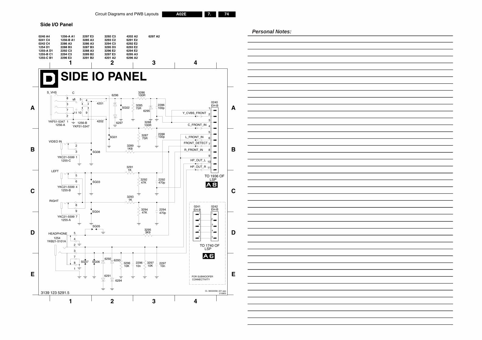
74A02E 7.Circuit Diagrams and PWB Layouts
YKB21-5101A1254 4
TO 1740 OFLSP
1 2 3 4
E E6291 FOR SUBWOOFERCONNECTIVITY
SG07
6294
62936292SG06
1
2
3
7
810n2297
10K3297
10n2296
10K3296
CL 36532058_021.eps2108033139 123 5291.5
Side I/O Panel
Y
CS_VHS
VIDEO IN
LEFT
SIDE IO PANEL
RIGHT
HEADPHONE
TO 1936 OFLSP
1 2 3 4
A
B
C
D
A
B
C
D
0240 A40241 C40242 C41254 D11255-A D11255-B C11255-C B1
1256-A A11256-B A12286 A32288 B32292 C32294 C32296 E3
2297 E33285 A33286 A33287 B33288 A33289 B23291 B2
3292 C33293 C23294 C33295 D33296 E23297 E34201 A2
4202 A26291 E26292 E26293 E26294 E26295 A36296 A2
6297 A2
4202
4
5
EH-B0241
1
2
3
4201
6297
6296
EH-B0242
1
2
3
4
5
6295
2288100p
9
2286100p
0240EH-B
1
10
11
2
3
4
5
6
7
8SG08
32953K9
2
7
3
8
1
32891K8
5
10
4
9
6
11
YKF51-53471256-A
75R3285
1256-BYKF51-5347
7
8
9
328775R
1255-CYKC21-5599 1
2
3
1255-AYKC21-5599
1255-BYKC21-5599 4
5
6
SG05
1K3293
SG01
SG04
SG03
SG02
5
2292470p
470p2294
47K3294
329247K
32911K
3286100R
3288100R
Y_CVBS_FRONT
C_FRONT_IN
L_FRONT_IN
R_FRONT_IN
HP_OUT_L
HP_OUT_R
FRONT_DETECT
Personal Notes:
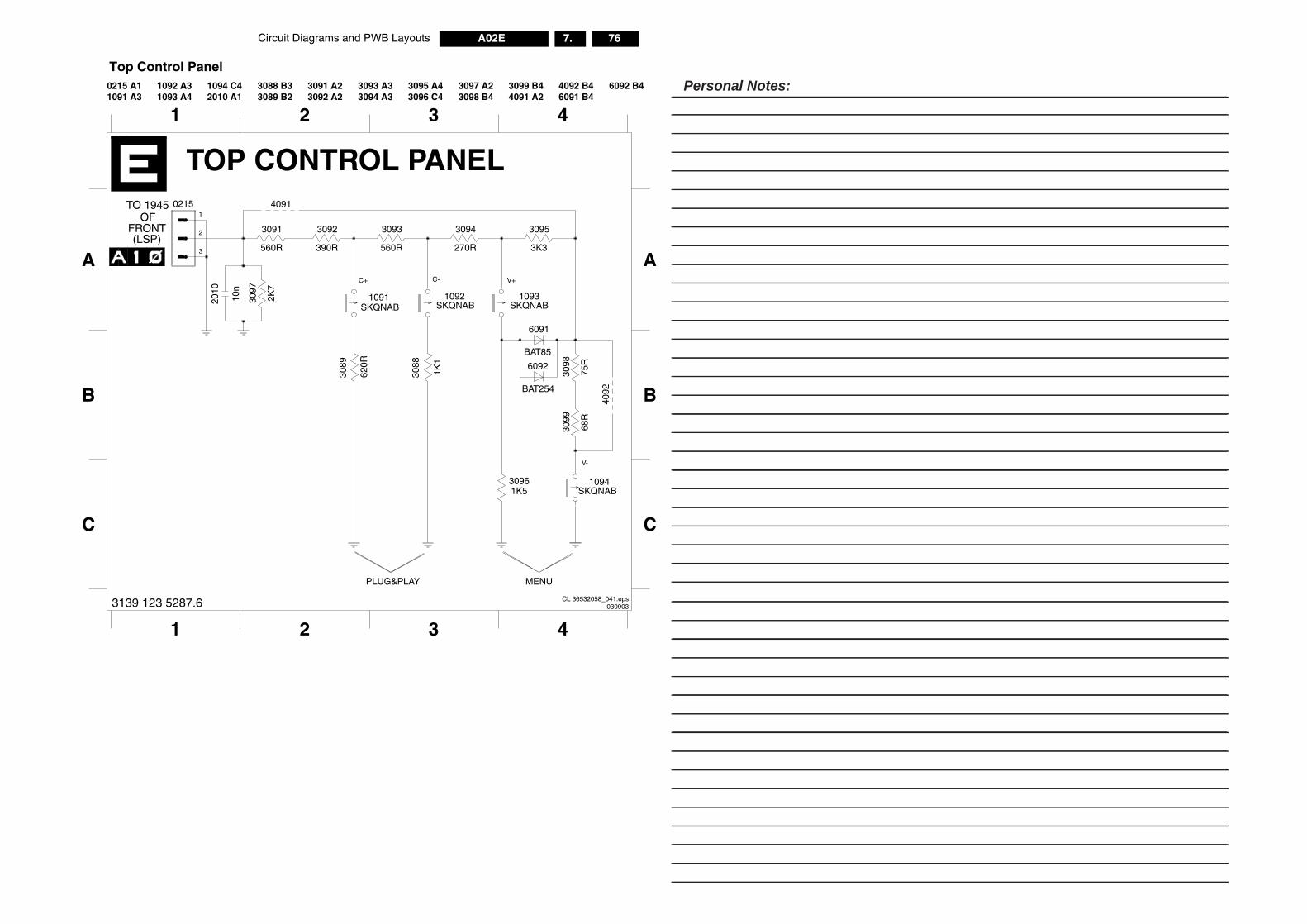
76A02E 7.Circuit Diagrams and PWB Layouts
Top Control Panel
TOP CONTROL PANEL
C+ C- V+
V-
TO 1945OF
FRONT(LSP)
PLUG&PLAY MENU
620R
1 2 3 4
1 2 3 4
A
B
C
A
B
C
0215 A11091 A3
1092 A31093 A4
1094 C42010 A1
3088 B33089 B2
3091 A23092 A2
3093 A33094 A3
3095 A43096 C4
3097 A23098 B4
3099 B44091 A2
4092 B46091 B4
6092 B4
1
2
3 560R10
n
2010
4091
6092
BAT254
4092
3088
1K1
3089
3098
75R
3099
68R
3097
2K7
1K53096
6091
BAT85
3K3
30953093
560R 270R
30943091
390R
3092
0215
1093SKQNAB
SKQNAB1094
SKQNAB SKQNAB10921091
CL 36532058_041.eps0309033139 123 5287.6
Personal Notes:
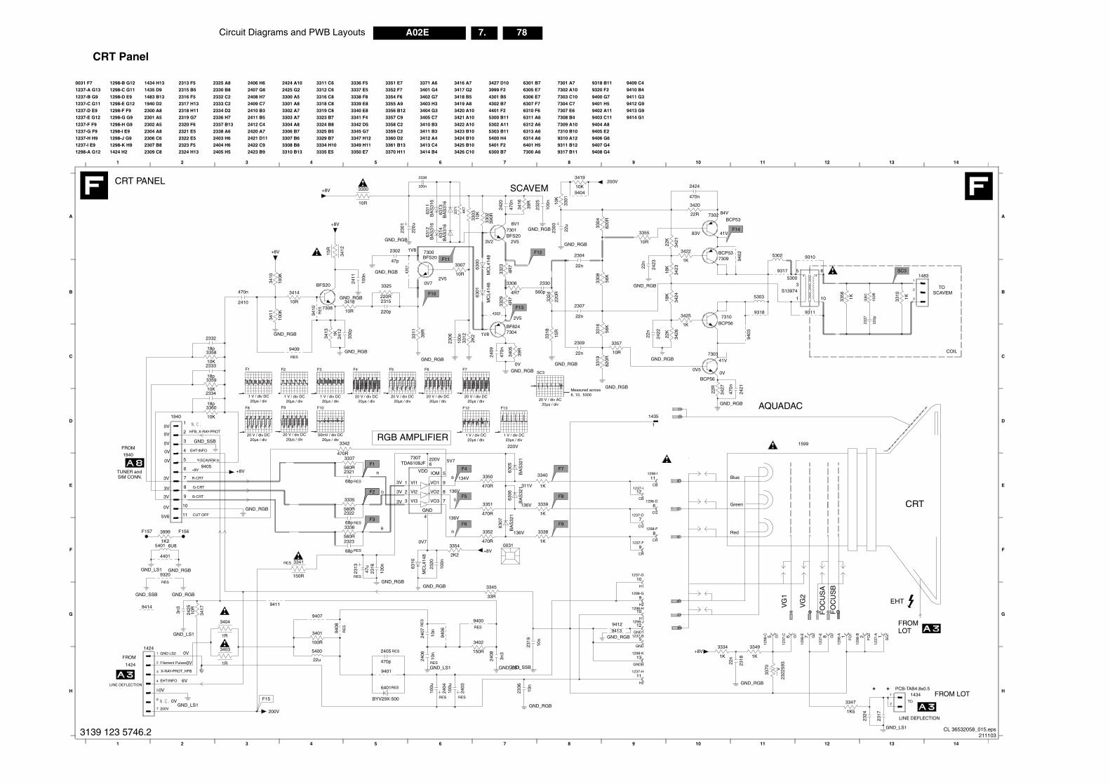
78A02E 7.Circuit Diagrams and PWB Layouts
V
TOSCAVEM
* *
CRT
QUADAC
VG
1
VG
2
FO
CU
SA
FO
CU
SB
EHT
FROMLOT
TO
LINE DEFLECTION
1599
FROM LOT
COIL
1 12 13 14
1 12 13 14
F
A
B
C
D
E
F
G
H
14831
2
3
S13974
5300
1 10
3
5 6
68p RES
2324
2K2
1K3310
3356
1K
9310
9311
4401
220p
2337
150R
3361
27
FG
1
1298
-A 1
FG
2
1298
-BG1
1298
-C 5 G2
1298
-E 8
SG
1
1237
-A 1G1
1237
-C 6 G2
1237
-E
CR+8V
GND_LS1
3370
2322
593
5302
9317 SC3
48
1K5
3347
2317
1434PCB-TAB4.8x0.5
1
2
CL 36532058_015.eps211103
FROM
1424
EHT-INFO
Filament Pulses
200V
GND LS2
LINE DEFLECTION
0V
0V
0V
0V
6V
1 2 3 4 5 6 7 8 9 10 1
G
H
7
2316
100n
2313
47u
RES
GND_RGB
9414
94129413
13
GND1
1298-J12
10
H2
1298-G9
GNDB
1298-K
H1
1298-H
11
1237-B5
H2
1237-H
H1
1237-G10
GND
3n3
2425
GND_LS1
10R
3417
9411
GND_RGBGND_SSB
RES
9320
+8V
GND_LS1
GND_RGB
GND_LS1
GND_RGBGND_RGB
GND_RGBGND_LS1
GND_SSB
GND_RGB
10n
2336
9408
RE
S
200V
9407
F15GND_LS1
10n
2319
150R
3402
3n3
2408
9400RES
10n
2406
RES
9406
RES
10n
2407
RE
S
2404
100u
RES
2403
100u6401
BYV29X-500
RES
470p
2405 RES
9401
5400
22u
3403
1R
100R
3401
3404
1R
33R
3345
14241
2
3
4
5
6
2320
100n
MC
L41
6310
3334
1K
22n
2318
3349
1K
3341
150R
RES
X-RAY-PROT_HFB
3139 123 5746.2
CRT Panel
Blue
Green
Red
R-CRT
G-CRT
B-CRT
CUT OFF
R
R
G
B
B
RGB AMPLIFIER
CRT PANEL
EHT-INFO
+8V
Y-SCAVEM ln
A
FROM
1940
TUNER andSIM CONN.
G
SCAVEM
0V7
136V
136V
134V
5V7220V
3V
3V
3V
220V
311V
136V
136V
41V
0V0V5
2V5
1V8
0V
0V72V5
1V8
8V1
2V53V2
84V
83V 41V
0V
0V
0V
0V
0V
3V
3V
3V
0V
5V6
6U8
1 2 3 4 5 6 7 8 9 10 1
A
B
C
D
E
0031 F7
1237-A G13
1237-B G9
1237-C G11
1237-D E9
1237-E G12
1237-F F9
1237-G F9
1237-H H9
1237-I E9
1298-A G12
1298-B G12
1298-C G11
1298-D E9
1298-E G12
1298-F F9
1298-G G9
1298-H G9
1298-I E9
1298-J G9
1298-K H9
1424 H2
1434 H13
1435 D9
1483 B13
1940 D2
2300 A8
2301 A5
2302 A5
2304 A8
2306 C6
2307 B8
2309 C8
2313 F5
2315 B5
2316 F5
2317 H13
2318 H11
2319 G7
2320 F6
2321 E5
2322 E5
2323 F5
2324 H13
2325 A8
2330 B8
2332 C2
2333 C2
2334 D2
2336 H7
2337 B13
2338 A6
2403 H6
2404 H6
2405 H5
2406 H6
2407 G6
2408 H7
2409 C7
2410 B3
2411 B5
2412 C4
2420 A7
2421 D11
2422 C9
2423 B9
2424 A10
2425 G2
3300 A5
3301 A8
3302 A7
3303 A7
3304 A8
3306 B7
3307 B6
3308 B8
3310 B13
3311 C6
3312 C6
3316 C8
3318 C8
3319 C8
3323 B7
3324 B8
3325 B5
3329 B7
3334 H10
3335 E5
3336 F5
3337 E5
3338 F8
3339 E8
3340 E8
3341 F4
3342 D5
3345 G7
3347 H12
3349 H11
3350 E7
3351 E7
3352 F7
3354 F6
3355 A9
3356 B12
3357 C9
3358 C2
3359 C2
3360 D2
3361 B13
3370 H11
3371 A6
3401 G4
3402 G7
3403 H3
3404 G3
3405 C7
3410 B3
3411 B3
3412 A4
3413 C4
3414 B4
3416 A7
3417 G2
3418 B5
3419 A8
3420 A10
3421 A10
3422 A10
3423 B10
3424 B10
3425 B10
3426 C10
3427 D10
3999 F2
4301 B5
4302 B7
4401 F2
5300 B11
5302 A11
5303 B11
5400 H4
5401 F2
6300 B7
6301 B7
6305 E7
6306 E7
6307 F7
6310 F6
6311 A6
6312 A6
6313 A6
6314 A6
6401 H5
7300 A6
7301 A7
7302 A10
7303 C10
7304 C7
7307 E6
7308 B4
7309 A10
7310 B10
9310 A12
9311 B12
9317 B11
9318 B11
9320 F2
9400 G7
9401 H5
9402 A11
9403 C11
9404 A8
9405 E2
9406 G6
9407 G4
9408 G4
9409 C4
9410 B4
9411 G3
9412 G9
9413 G9
9414 G1
F7
4R7
3329
2325
100n
RES
2323
GND_SSB
4R7
3323
3352
470R3354 0031
10R
3357
GND_RGB
15R
3412
7307TDA6108JF
4GND
IOM 5VDD
3308
56K
3318
2300
22u
15R
2420
39R
3416
+8V
200V
+8V
3312
2K2
100n
2306
47p
470n
BA
S31
663
1463
13B
AS
316
5401
BA
S31
663
1263
11B
AS
316
4K7
3371
330n
2338
4301
4302
9404
6
CR
1298-F8
1298-I11
CG
1298-D
CB
9
12
CG
1237-D7
1237-F
9403
CB
1237-I
9402
GND_RGB
GND_RGB
7310BCP56
10K
3419
22R
3420
470n
2424
10R
3418
22R
3427
470n
2421
1K
3425
3424
18K
3426
1K
3422
22K
3421
22K
2423
22n
18K
3423
22n
2422
BCP537309
RE
S
+8V
RES
9409
9410
+8V
1K3413
GND_RGB
GND_RGB
3411
100K
GND_RGB
24107308
BFS2010
0K
3410
470n
330p
2412
10R
3414
2411
100n
2409
470n
3405
39R
GND_RGB
GND_RGB
GND_RGB
GND_RGB
GND_RGB
GND_RGB
GND_RGB
GND_RGB
GND_RGB
9405
F156F157
1K2
3999
18p
2334
820R
3304
18p
233310K
335818p
2332
3360
10K
3359
10K
F6
F2
F1F4
F5
F13
F11
F10
F3
F8
F9
F14
F12
560p
2330
220R
3325
5303
9318
3324
220R
6300
MC
L414
8
6301
MC
L414
8
BF8247304
2315
220p
3355
10R
2321
68p RES
68p
2322
22n
2307
22n
2309
56K
3316
3319
820R
22n
2304
3301
10K
3306
4R7
BCP56
7303
BFS207301
BCP537302
3307
10R
3303
10K
2302
3302
390R
6306
BA
S32
1B
AS
321
6305
BA
S32
1
6307
3351
470R
3350
470R
1435
1
6
VI11
VI22
VI33
VO1 9
VO2 8
VO3 7
3338
1K
1K
3340
560R
3337
1K
3339
3336
560R
470R
3342
560R
3335
1
10
11
2
3
4
5
6
7
8
9
39R
3311
1940
BFS207300
3300
10R
2301
220u
HFB_X-RAY-PROT
F1
1 V / div DC20µs / div
F2
Measured across 6, 10, 53001 V / div DC
20µs / div
F3
1 V / div DC20µs / div
F4
20 V / div DC20µs / div
F5
20 V / div DC20µs / div
F6
20 V / div DC20µs / div
F7
20 V / div DC20µs / div
F8
20 V / div DC20µs / div
F9
20 V / div DC20µs / div
F10
50mV / div DC20µs / div
F12
1 V / div DC20µs / div
F13
1 V / div DC20µs / div
SC3
20 V / div AC20µs / div
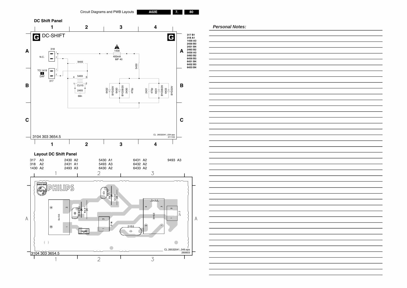
80A02E 7.Circuit Diagrams and PWB Layouts
CL 26532041_049.eps2606033104 303 3654.5
DC Shift Panel
Layout DC Shift Panel
317 B1
C
B
40
1 2 3 4
1 2 3 4
A
C
B
A
DC-SHIFT
TO 1419
DAF
N.C.
6433 B46432 B36431 B46430 B35493 B25430 A3
318 A11430 A32430 B32431 B42493 B2
1 2
4 3
9493
5493
CU15
68n
2493
BY
228/
20
6431
BY
D33
V
6433
2431
470p
6432
BY
D33
V
470p
2430
6430
BY
228/
20
2
MP400mA
1430
5430
1
2
317
1
318
CL 26532041_034.eps211103
I
3104 303 3654.5
317 A3318 A21430 A2
2430 A22431 A12493 A3
5430 A15493 A36430 A2
6431 A26432 A26433 A2
9493 A3
Personal Notes:
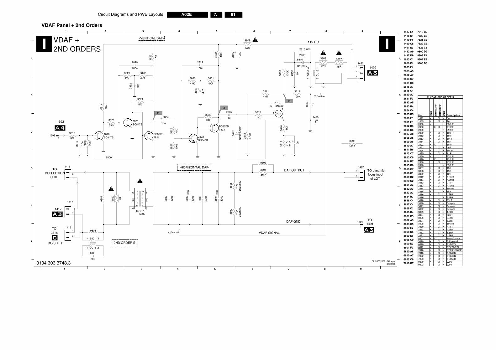
Circuit Diagrams and PWB Layouts 81A02E 7.
3998
100R
14971
2
1491
3
1491
1
3898 D5
3897 E2
3833 C5
3832 A5
3831 B5
3830 B4
5800 E3
5801 F2
5810 A8
6810 A7
6812 C6
7810 B7
7818 C2
7820 C3
7821 C3
7822 C5
7823 C5
9800 D2
9803 F2
9804 E2
9805 D6
TO
1492
2891 E5
2892 B3
3805 D6
3807 A8
3808 A8
3809 A6
1417 E1
1418 D1
1419 F1
1490 C8
1491 E9
1492 A9
1497 D9
1693 C1
2800 E4
2803 E4
2809 A5
2812 A7
2813 C7
2814 B8
2816 A7
2818 C1
2820 A3
2821 F2
2822 A5
2823 B4
2824 C4
2825 B5
9
9
TO dynamic
A
2890 E5
B
C
D
E
F
3810 A7
3811 B6
3812 C7
3813 C6
3814 B7
3815 B6
3816 C7
3818 C1
3819 B2
3820 C2
3821 A3
3822 A3
3823 A3
3824 B3
3826 C4
3827 C4
3828 C1
of LOTfocus input
3899 E5
3998 C9
14921
2
CU151 2
CL 26532067_040.eps260603
Item 29R
F
28R
F/32
RF
34R
F/38
RF
36R
F
Description
[I] VDAF+2ND ORDER S
1492 X X X 3p1693 X X X 1p2800 X 330pF2800 X X 470pF2800 X 390pF2809 X X X 100F2812 X X X 10nF2813 X X X 10F2814 X X X 1nF2821 X X 68nF2822 X X X 4nF2824 X X X 10F2825 X X X 1F2890 X 270pF2890 X 220pF2890 X 470pF2890 X 390pF3807 X X X 15R3808 X X X 15R3809 X X X 10R3810 X X X 470kR3811 X X X 4.7MR3812 X X X 27kR3813 X X X 470kR3814 X X X 100kR3815 X X X 1kR3816 X X 4.7kR3816 X 2.2kR3818 X X X 33kR3820 X X X Jumper3821 X X X Jumper3822 X X X Jumper3823 X X X 1.5kR3824 X X X 33kR3826 X X X 3.3kR3827 X X X 5.6kR3828 X X X 100kR3830 X X X 47kR3831 X X X 4.7kR3832 X X X 1.8kR3833 X X X 4.7kR5801 X X Transformer5810 X X X Bridge coil6810 X X X BYD33V6812 X X X BZX79-C227810 X X X STP3NB80FP7818 X X X BC847B7822 X X X BC847B7823 X X X BC857B9800 X X X Wire9803 X X Wire
87654321
2821
68n
3104 303 3748.3
VDAF Panel + 2nd Orders
VV
9805
4M7
3805
3821
47K
3815
1K
3813
470K
2820
100n
2813
10u
3830
47K
11693
2803
330p
100K
3828
2825
1u
I2
2892
4u7
TO
V_Parabool
RES
2891
2818
10n
2809
100u
2822
100n
2823
4u7
3814
100K
5K6
3827
TODEFLECTION
-HORIZONTAL DAF-
DC-SHIFT
VDAF SIGNAL
11V DC
V_Parabool
3812
27K
87654321
-2ND ORDER S-
RE
S
A
B
C
D
E
F
DAF GND
DAF OUTPUT
COIL
1693
0318
-VERTICAL DAF-
1417
RE
S
S219755800
1
2
34
5
6
330p
3826
4K7
330p
2814 1n
2800
9803
I1
I3
1417
1
2
15R
38073808
22R
3809
10R
3818
4K7
1K8
3832
9800
2890
270p
2812
10n
14191
2
7821BC857B
7822BC847B
7818BC847B
3831
4K7
3833
4K7
3810
470K
7823BC857B
9804
3897
1R1490
1
1418
1
2
58014 3
3811
4M73824
4K7
3816
4K7
2816
220p
12
43
BYD33V
6810
2322
592
3899
CU
15
5810
2824
10u
3898
2322
592
3819
4K7
7820BC847B
3820
3K3
3822
4K7
6812
BZ
X79
-C22
STP3NB807810
21
3
3823
1K8
2ND ORDERS +VDAF
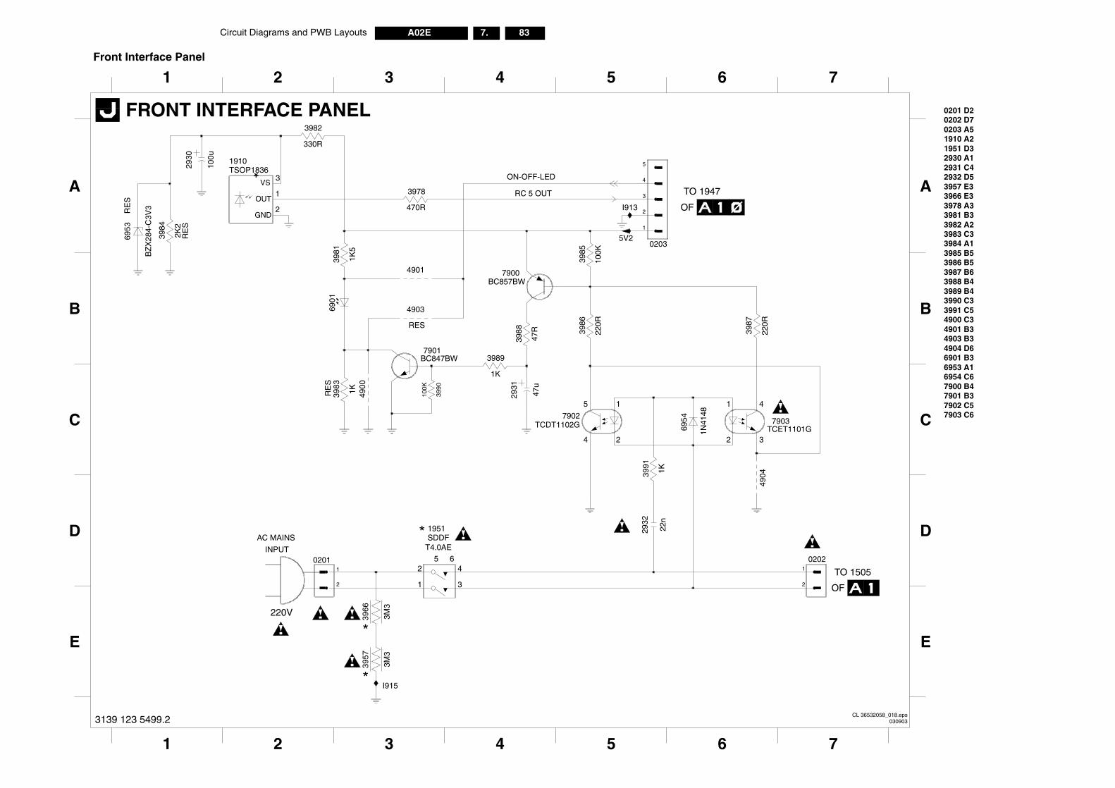
Circuit Diagrams and PWB Layouts 83A02E 7.
TO 1505
OF
7
7
A
B
C
D
E
0201 D20202 D70203 A51910 A21951 D32930 A12931 C42932 D53957 E33966 E33978 A33981 B33982 A23983 C33984 A13985 B53986 B53987 B63988 B43989 B43990 C33991 C54900 C34901 B34903 B34904 D66901 B36953 A16954 C67900 B47901 B37902 C57903 C6
7903TCET1101G
220R
5 60201 02021
2
CL 36532058_018.eps030903
220V
*
*
1 2 3 4 5 6
E
I915
1 3
2 4
3M3
3957
1
2
3M3
3966
3139 123 5499.2
Front Interface Panel
T4.0AEAC MAINS
INPUT
FRONT INTERFACE PANEL
*
*
RE
S
RE
S
RE
SRES
ON-OFF-LED
RC 5 OUT
1 2 3 4 5 6
A
B
C
D
TO 1947
OF
100K
3990
22n
2932
I913
100K
7902TCDT1102G
15
4 2
1K3991
4904
6954
1N41
48
BZ
X28
4-C
3V3
2K2
3984
6953
100u
2930
470R
3978
330R
3982
1K5
3981
4903
4901
1K3983
4900
1 4
32
BC847BW7901
1K
3989
47u
2931
3987
47R
3988 22
0R
3986
3985
BC857BW7900
1951SDDF
6901
TSOP18361910
2GND
1OUT
3VS
1
2
3
4
5
5V20203
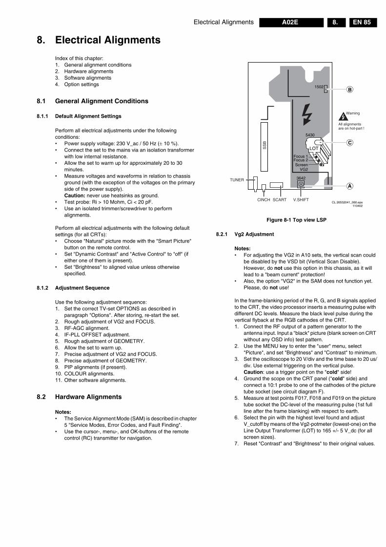
Electrical Alignments EN 85A02E 8.
8. Electrical Alignments
Index of this chapter:1. General alignment conditions2. Hardware alignments3. Software alignments4. Option settings
8.1 General Alignment Conditions
8.1.1 Default Alignment Settings
Perform all electrical adjustments under the following conditions:• Power supply voltage: 230 V_ac / 50 Hz (± 10 %). • Connect the set to the mains via an isolation transformer
with low internal resistance.• Allow the set to warm up for approximately 20 to 30
minutes.• Measure voltages and waveforms in relation to chassis
ground (with the exception of the voltages on the primary side of the power supply).Caution: never use heatsinks as ground.
• Test probe: Ri > 10 Mohm, Ci < 20 pF.• Use an isolated trimmer/screwdriver to perform
alignments. Perform all electrical adjustments with the following default settings (for all CRTs):• Choose "Natural" picture mode with the "Smart Picture"
button on the remote control.• Set "Dynamic Contrast" and "Active Control" to "off" (if
either one of them is present).• Set "Brightness" to aligned value unless otherwise
specified.
8.1.2 Adjustment Sequence
Use the following adjustment sequence:1. Set the correct TV-set OPTIONS as described in
paragraph "Options". After storing, re-start the set.2. Rough adjustment of VG2 and FOCUS.3. RF-AGC alignment.4. IF-PLL OFFSET adjustment.5. Rough adjustment of GEOMETRY.6. Allow the set to warm up.7. Precise adjustment of VG2 and FOCUS.8. Precise adjustment of GEOMETRY.9. PIP alignments (if present).10. COLOUR alignments.11. Other software alignments.
8.2 Hardware Alignments
Notes: • The Service Alignment Mode (SAM) is described in chapter
5 "Service Modes, Error Codes, and Fault Finding". • Use the cursor-, menu-, and OK-buttons of the remote
control (RC) transmitter for navigation.
Figure 8-1 Top view LSP
8.2.1 Vg2 Adjustment
Notes: • For adjusting the VG2 in A10 sets, the vertical scan could
be disabled by the VSD bit (Vertical Scan Disable). However, do not use this option in this chassis, as it will lead to a "beam current" protection!
• Also, the option "VG2" in the SAM does not function yet. Please, do not use!
In the frame-blanking period of the R, G, and B signals applied to the CRT, the video processor inserts a measuring pulse with different DC levels. Measure the black level pulse during the vertical flyback at the RGB cathodes of the CRT.1. Connect the RF output of a pattern generator to the
antenna input. Input a "black" picture (blank screen on CRT without any OSD info) test pattern.
2. Use the MENU key to enter the "user" menu, select "Picture", and set "Brightness" and "Contrast" to minimum.
3. Set the oscilloscope to 20 V/div and the time base to 20 us/div. Use external triggering on the vertical pulse.Caution: use a trigger point on the "cold" side!
4. Ground the scope on the CRT panel ("cold" side) and connect a 10:1 probe to one of the cathodes of the picture tube socket (see circuit diagram F).
5. Measure at test points F017, F018 and F019 on the picture tube socket the DC-level of the measuring pulse (1st full line after the frame blanking) with respect to earth.
6. Select the pin with the highest level found and adjust V_cutoff by means of the Vg2-potmeter (lowest-one) on the Line Output Transformer (LOT) to 165 +/- 5 V_dc (for all screen sizes).
7. Reset "Contrast" and "Brightness" to their original values.
CL 26532041_060.eps110402
SS
B
V.SHIFTCINCH SCART
TUNER 3642
1502
5430
Focus 2Focus 1
ScreenVG2
LOT
Warning
All alignmentsare on hot-part !
A
B
C
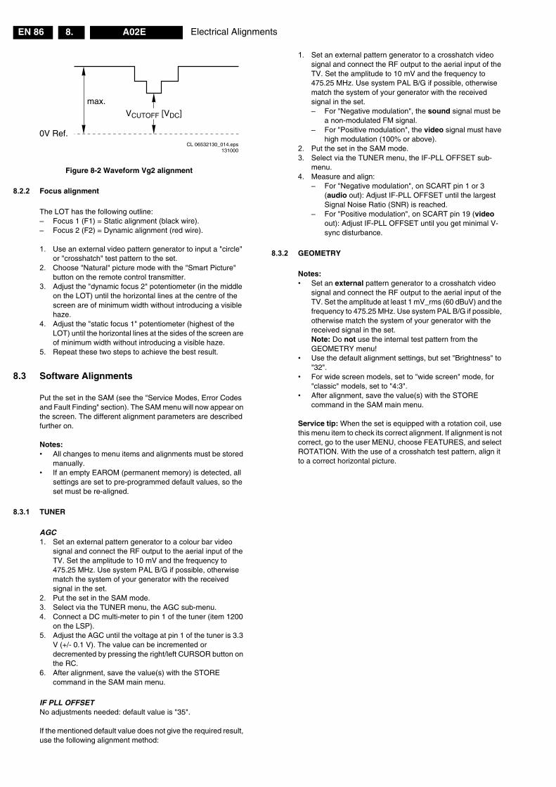
Electrical AlignmentsEN 86 A02E8.
Figure 8-2 Waveform Vg2 alignment
8.2.2 Focus alignment
The LOT has the following outline:– Focus 1 (F1) = Static alignment (black wire).– Focus 2 (F2) = Dynamic alignment (red wire). 1. Use an external video pattern generator to input a "circle"
or "crosshatch" test pattern to the set.2. Choose "Natural" picture mode with the "Smart Picture"
button on the remote control transmitter.3. Adjust the "dynamic focus 2" potentiometer (in the middle
on the LOT) until the horizontal lines at the centre of the screen are of minimum width without introducing a visible haze.
4. Adjust the "static focus 1" potentiometer (highest of the LOT) until the horizontal lines at the sides of the screen are of minimum width without introducing a visible haze.
5. Repeat these two steps to achieve the best result.
8.3 Software Alignments
Put the set in the SAM (see the "Service Modes, Error Codes and Fault Finding" section). The SAM menu will now appear on the screen. The different alignment parameters are described further on. Notes:• All changes to menu items and alignments must be stored
manually.• If an empty EAROM (permanent memory) is detected, all
settings are set to pre-programmed default values, so the set must be re-aligned.
8.3.1 TUNER
AGC1. Set an external pattern generator to a colour bar video
signal and connect the RF output to the aerial input of the TV. Set the amplitude to 10 mV and the frequency to 475.25 MHz. Use system PAL B/G if possible, otherwise match the system of your generator with the received signal in the set.
2. Put the set in the SAM mode.3. Select via the TUNER menu, the AGC sub-menu. 4. Connect a DC multi-meter to pin 1 of the tuner (item 1200
on the LSP). 5. Adjust the AGC until the voltage at pin 1 of the tuner is 3.3
V (+/- 0.1 V). The value can be incremented or decremented by pressing the right/left CURSOR button on the RC.
6. After alignment, save the value(s) with the STORE command in the SAM main menu.
IF PLL OFFSETNo adjustments needed: default value is "35". If the mentioned default value does not give the required result, use the following alignment method:
1. Set an external pattern generator to a crosshatch video signal and connect the RF output to the aerial input of the TV. Set the amplitude to 10 mV and the frequency to 475.25 MHz. Use system PAL B/G if possible, otherwise match the system of your generator with the received signal in the set.– For "Negative modulation", the sound signal must be
a non-modulated FM signal.– For "Positive modulation", the video signal must have
high modulation (100% or above).2. Put the set in the SAM mode.3. Select via the TUNER menu, the IF-PLL OFFSET sub-
menu. 4. Measure and align:
– For "Negative modulation", on SCART pin 1 or 3 (audio out): Adjust IF-PLL OFFSET until the largest Signal Noise Ratio (SNR) is reached.
– For "Positive modulation", on SCART pin 19 (video out): Adjust IF-PLL OFFSET until you get minimal V-sync disturbance.
8.3.2 GEOMETRY
Notes: • Set an external pattern generator to a crosshatch video
signal and connect the RF output to the aerial input of the TV. Set the amplitude at least 1 mV_rms (60 dBuV) and the frequency to 475.25 MHz. Use system PAL B/G if possible, otherwise match the system of your generator with the received signal in the set.Note: Do not use the internal test pattern from the GEOMETRY menu!
• Use the default alignment settings, but set "Brightness" to "32".
• For wide screen models, set to "wide screen" mode, for "classic" models, set to "4:3".
• After alignment, save the value(s) with the STORE command in the SAM main menu.
Service tip: When the set is equipped with a rotation coil, use this menu item to check its correct alignment. If alignment is not correct, go to the user MENU, choose FEATURES, and select ROTATION. With the use of a crosshatch test pattern, align it to a correct horizontal picture.
0V Ref.CL 06532130_014.eps
131000
VCUTOFF [VDC]max.
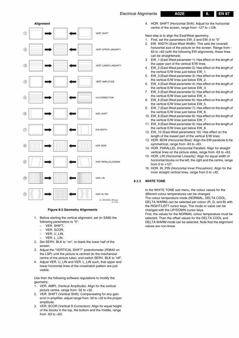
Electrical Alignments EN 87A02E 8.
Alignment
Figure 8-3 Geometry Alignments
1. Before starting the vertical alignment, set (in SAM) the following parameters to "0":– VER. SHIFT, – VER. SCOR,– VER. U_LIN,– VER. L_LIN.
2. Set SERV. BLK to "on", to blank the lower half of the screen.
3. Adjust the "VERTICAL SHIFT" potentiometer (R3642 on the LSP) until the picture is centred (to the mechanical centre of the picture tube), and switch SERV. BLK to "off".
4. Adjust VER. U_LIN and VER. L_LIN such, that upper and lower horizontal lines of the crosshatch pattern are just visible.
Use then the following software regulations to modify the geometry:1. VER. AMPL (Vertical Amplitude): Align for the vertical
picture centre, range from -32 to +32.2. VER. SHIFT (Vertical Shift): Compensating for any gain
error in amplifier, adjust range from -32 to +32 to the proper amplitude.
3. VER. SCOR (Vertical S-Correction): Align for equal height of the blocks in the top, the bottom and the middle, range from -63 to +63.
4. HOR. SHIFT (Horizontal Shift): Adjust for the horizontal centre of the screen, range from -127 to +128.
Next step is to align the East/West geometry.1. First, set the parameters EW_5 and EW_6 to "0"2. EW. WIDTH (East-West Width): This sets the (overall)
horizontal size of the picture on the screen. Range from -63 to +63 (with the following EW alignments, these lines can be straightened).
3. EW_1 (East-West parameter 1): Has effect on the length of the upper part of the vertical E/W lines.
4. EW_2 (East-West parameter 2): Has effect on the length of the vertical E/W lines just below EW_1.
5. EW_3 (East-West parameter 3): Has effect on the length of the vertical E/W lines just below EW_2.
6. EW_4 (East-West parameter 4): Has effect on the length of the vertical E/W lines just below EW_3.
7. EW_5 (East-West parameter 5): Has effect on the length of the vertical E/W lines just below EW_4.
8. EW_6 (East-West parameter 6): Has effect on the length of the vertical E/W lines just below EW_5.
9. EW_7 (East-West parameter 7): Has effect on the length of the vertical E/W lines just below EW_6.
10. EW_8 (East-West parameter 8): Has effect on the length of the vertical E/W lines just below EW_7.
11. EW_9 (East-West parameter 9): Has effect on the length of the vertical E/W lines just below EW_8.
12. EW_10 (East-West parameters 10): Has effect on the length of the lowest part of the vertical E/W lines.
13. HOR. BOW (Horizontal Bow): Align the EW parabola to be symmetrical, range from -63 to +63.
14. HOR. PARALLEL (Horizontal Parallel): Align for straight vertical lines on the picture sides, range from -63 to +63.
15. HOR. LIN (Horizontal Linearity): Align for equal width of horizontal blocks on the left, the right and the centre, range from 0 to +127.
16. HOR. IN_PIN (Horizontal Inner Pincushion): Align for the inner straight vertical lines, range from 0 to +32.
8.3.3 WHITE TONE
In the WHITE TONE sub menu, the colour values for the different colour temperatures can be changed.The colour temperature mode (NORMAL, DELTA COOL, DELTA WARM) can be selected per colour (R, G, and B) with the RIGHT/LEFT cursor keys. The mode or value can be changed with the UP/DOWN cursor keys.First, the values for the NORMAL colour temperature must be selected. Then the offset values for the DELTA COOL and DELTA WARM mode can be selected. Note that the alignment values are non-linear.
CL 36532058_084.eps211103
4
2
6
7
9
8
VERT. AMPLITUDE
VERT UPPER LINEARITY
HOR. SHIFT
E/W WIDTH
11 HOR. IN. PIN
HOR. PARALLELOGRAM
HOR. BOW
3 VERT LOWER LINEARITY
5 V.S-CORRECTION
10 HOR. LIN
1 VERT. SHIFT
Electrical AlignmentsEN 88 A02E8.
AlignmentNo adjustments needed. Use the given default values:
Table 8-1 White tone alignment (default values)
If the mentioned default value does not give the required result, use the following alignment method:1. Set the external pattern generator to a 100% white pattern,
and connect the RF output to the aerial input of the TV. Set the amplitude at least 1 mV_rms (60 dBuV) and the frequency to 475.25 MHz. Use system PAL B/G if possible, otherwise match the system of your generator with the received signal in the set.
2. Set "Smart Picture" to "Natural".3. Set "Dynamic NR" to "off".4. Put the set in the SAM mode.5. Select via the WHITE TONE menu, the PATTERN sub-
menu. 6. Set PATTERN to "on".7. Set NORMAL GREEN to "32".8. Measure with the colour analyser (Minolta CA100 Colour
Analyser or equivalent), calibrated with the spectra, on the centre of the screen.
9. Adjust with the cursor left/right command the Red and Blue register for the right xy-coordinates (see the table below).
10. Repeat the white tone adjustment also for the colour temperatures COOL and WARM.
Table 8-2 White tone alignment (with colour analyser)
8.3.4 SOUND
No adjustments needed. Use the given default values:• PRESCALE LEVEL
– FM: "+1".– NICAM: "+3".– EXTAM Gain: "0".– PIPMONO: "0".– ExtLR-in: "0".
• TRESHOLD LEVEL– Over Mod Tresh: "+3dB".– NIC ErrLmt_Hi: "60".– NIC ErrLmt_Lo: "20".– NoiseTres SC2: "+2".– NoiseHyst SC2: "+4".
• EFFECTS LEVEL
– BMT CutOffFrq: "50Hz".– Incredible SND: "60%".– VDolby: "100%".
8.3.5 SMART SETTINGS
No adjustments needed. Use the given default values:
Table 8-3 Smart settings (default values)
8.4 Option Settings
8.4.1 Introduction
The microprocessor communicates with a large number of I2C ICs in the set. To ensure good communication and to make digital diagnosis possible, the microprocessor has to know which ICs to address. The presence / absence of these specific ICs (or functions) is made known by the option codes. Notes: • After changing the option(s), save them with the STORE
command.• All changes are disregarded when the OPTIONS submenu
is left without using the STORE command.• The new option setting is only active after the TV is
switched "off" and "on" again with the Mains switch (the EAROM is then read again).
8.4.2 Changing options
Options are used to control the presence / absence of certain features and hardware. There are two ways to change the option settings. All changes in the option settings are saved by selecting STORE and pressing the CURSOR RIGHT key. Some changes will only take affect after the set has been switched OFF and ON with the mains switch (cold start).
Changing multiple options by changing option byte valuesOption Bytes (OB) makes it possible to set all options very fast. An option byte represents a number of different options. All
Parameter28
PW
8609
/12
29P
T85
09/1
2
32P
W86
09/1
2Normal Red -4 +11 +1
Normal Green -9 +4 -7
Normal Blue -6 +12 -2
Red BL Offset 7
Green BL Offset 7
Blue BL Offset 7
Delta Cool Red 7
Delta Cool Green 15
Delta Cool Blue 33
Delta Warm Red 2
Delta Warm Green 3
Delta Warm Blue 7
White D mode Temperature DUV x y
Normal 8500 K +-0.004 288 +/- 4 300 +/- 4
Cool 11500 K +-0.005 273 +/- 5 282 +/- 5
Warm 7000 K +-0.005 305 +/- 5 312 +/- 5
Smart setting Default
RICH BGT 55
COL 55
CON 100
SHP 6
HUE 51
NATURE BGT 51
COL 48
CON 80
SHP 5
HUE 51
SOFT BGT 49
COL 45
CON 65
SHP 4
HUE 51
MULTI BGT 51
COL 48
CON 85
SHP 6
HUE 51
BGT= Brightness, COL= Colour,CON= Contrast, SHP= Sharpness,HUE= Hue (not valid for Europe).
Electrical Alignments EN 89A02E 8.
options are controlled via eight option bytes (OB0 to OB7). Select an Option Byte you want to change with the CURSOR UP/DOWN keys, and key in the new value. See table for more details. An explanation per option is listed in paragraph "Option Bit Definition".
Changing a single optionIt is also possible to change an option one at a time. Therefore, select the option with the CURSOR UP/DOWN keys and change its setting with the LEFT/RIGHT keys.
8.4.3 Option Settings
In the table, you will find the option settings.
Table 8-4 Option bit overview
8.4.4 Option Bit Definition
SourcesAV3: Side AV source.Function: Disable/Enable side AV source.Values: OFF= Disabled, side AV source is not available. ON= Enabled, side AV source is available. SCT3: SCART 3 input.Function: Disable/Enable Scart3 input.Values: OFF= Disabled. ON= Enabled.
VideoASPR: Aspect Ratio Setting.Function: Select between 4 by 3 or 16 by 9 set.Values: OFF= 4 by 3 set. ON= 16 by 9 set. DNR: Dynamic Noise Reduction.Function: Disable/Enable (Dynamic) Noise Reduction function.Values: OFF=Disabled. ON= Enabled. BBD: Black Bar Detection.Function: Disable/Enable Black Bar Detection.Values: OFF=Disabled, Black Bar Detection not available. ON= Enabled, Black Bar Detection available.Note: The Auto Screen Fit will not be included in the picture size loop when BBD is OFF. ASF: Auto Screen Fit.Function: Disable/Enable Auto Screen Fit.Values: OFF=Disabled, Auto Screen Fit is not available. ON= Enabled, Auto Screen is Fit available. CZOM: Continuous Zoom.Function: Disable/Enable Continuous Zoom.Values: OFF=Disabled. ON= Enabled. HSHT: Heading Shift.Function: Disable/Enable Heading Shift.Values: OFF=Disabled. ON= Enabled. SSHT: Subtitle Shift.Function: Disable/Enable Subtitle Shift.Values: OFF=Disabled. ON= Enabled. APC: Auto Picture Control (Auto TV).Function: Disable/Enable Auto picture control.Values: OFF= Disabled. ON= Enabled. WSSB: Wide Screen Signalling Bit.Function: Disable/Enable Wide screen Signalling bit function.Values: OFF= Disabled. ON= Enabled. ROTI: Rotation Tilt.Function: Change the tilt level of picture tube.Values: OFF= Disabled, menu item ROTATION is not available. ON= Enabled, menu item ROTATION is available. DGSC: Digital Scan.Function: Enable/Disable the Digital Scan in the DIGITAL OPT menu.Values: OFF= Disabled, menu item DIG SCAN is not available. ON= Enabled, menu item DIG SCAN is available. SCAVM: SCAVEM.Function: Enable/Disable SCAVEM.Values: OFF= Disabled. ON= Enabled.
AudioAAVL: Automatic Volume Level control.Function: Disable/Enable automatic volume leveller function.Values: OFF=Disabled, menu item AVL is not available. ON= Enabled, menu item AVL is available.
Byt
e n
um
ber
Bit
nu
mb
er
Dec
imal
val
ue
Nam
e
28P
W86
09/1
2
29P
T85
09/1
2
32P
W86
09/1
2
OB1
1 2 SCAVM 1 1 15 32 RCMX 0 0 06 64 EQTO 0 0 08 256 WSSB 1 0 1
12 4096 DGSC 1 1 114 16384 SSHT 1 0 1
OB2
5 32 DBYV 1 1 19 512 P50 0 0 0
11 2048 QPEAK 0 0 012 4096 EPG 0 0 0
OB3
0 1 AV3 1 1 11 2 SCT3 0 0 05 32 SOSD 0 0 08 256 ASPR 1 0 19 512 ROTI 1 0 1
OB43 8 PITN * 0 0 04 16 PITN * 0 0 0
OB5 6 64 AAVL 1 1 1
OB84 16 PIPC 0 0 05 32 PIPT 0 0 0
OB9
0 1 APC 1 1 15 32 VMOD 0 0 07 128 TIME 1 1 18 256 DNR 1 1 19 512 BBD 0 0 0
10 1024 ASF 0 0 0
OB10
5 32 UKPNP 0 0 06 64 DTXT 1 0 18 256 SBNP 1 1 19 512 AUSB 0 0 0
10 1024 CZOM 1 0 111 2048 HSHT 1 0 114 16384 CHLK 1 1 1
OB119 512 T1H0 1 1 1
13 8192 FAPG 1 1 114 16384 ACI 1 1 1
OB12 8 256 PLST 1 1 1
OB13
0 1 T2H5 1 1 12 4 T12H 1 1 13 8 EWEU 0 0 07 128 SMCK 1 1 18 256 ATS 1 1 1
* = There are 2 bits for this option: 00 = Philips, 01 = Other Unused options have a default value of "0"
Electrical AlignmentsEN 90 A02E8.
DBYV: Dolby Virtual.Function: Select surround setting.Values: OFF= Disabled, DOLBY VIRTUAL setting is not available. ON= Enabled, DOLBY VIRTUAL setting is available.Note: Incredible surround & Dolby virtual are mutually exclusive. EQTO: Equalizer or Tone control.Function: Selection between Equalizer and Tone control (Bass and Treble).Values: OFF= Tone control (Bass and Treble). ON= Equalizer.Note: Equalizer and Tone (Bass and treble) control are mutually exclusive. QPEAK: AV Sound Mode detection.Function: The current Sound Mode detection in AV is not working correctly. The optimal threshold value for the correct sound mode detection is still being investigated. Therefore, this is needed to disable the Sound Mode detection in AV until the correct threshold is identified.Value: OFF= Disabled, AV sound auto detection is not available. ON= Enabled. AV sound auto detection is available.
TuningPITN: Philips Tuner.Function: Choose the tuner type that is configured in the hardware.Values: OFF= Disabled, ALPS compatible tuner is used. ON= Enabled, Philips compatible tuner is used.
InstallationACI: Automatic Channel Installation.Function: Disable/Enable automatic channel installation.Values: OFF= Disabled Automatic Channel Installation. ON= Enabled Automatic Channel Installation.Note: Download present program when ACI is ON. ATS: Automatic Tuning System.Function: Disable/Enable automatic tuning system.Values: OFF= Disabled, automatic tuning system is ignored. ON= Enabled Automatic Tuning System, sort the program in an ascending order starting from Program 1.Note: Sort the program in an ascending order starting from Program 1 when ATS is ON. VMOD: Virgin Mode.Function: Disable/Enable virgin mode.Values: OFF= Disabled, cannot access virgin mode. ON= Enabled, can access virgin mode.Note: Plug and Play menu item will be displayed to perform installation at the initial start up of the TV when MOD is ON and after installation is done, VMOD will be automatically set to OFF. UKPNP: UK Plug and Play.Function: Disable/Enable UK’s default Plug and Play setting.Values: OFF= Disabled, UK’s default Plug and Play setting is not available. ON= Enabled, UK’s default Plug and Play setting is available.Note: When UKPNP and VMOD are ON at the initial set-up, LANGUAGE= ENGLISH, COUNTRY= GREAT BRITAIN and after auto store is complete, VMOD will be set automatically to OFF while UKPNP remain ON.
Program SelectionPLST: Program List.Function: Disable/Enable Program List function.Values: OFF= Disabled, the access to Program List Command is ignored. ON= Enabled, the access to Program List Command is processed.
Picture In PicturePIPC: PIP Control.
Function: Disable/Enable submenu to adjust PIP Picture settingsValues: OFF= Disabled, PIP feature is not available. ON= Enabled, PIP feature is available Note: PIP is present in FEATURES submenu when PIPC is ON. When PIPC is switched OFF, bits PIPT, W4X3, and W169 must be automatically set to OFF. PIPT: PIP Tuner.Function: To determine the presence of second tuner.Values: OFF= Disabled, second tuner is not available. ON= Enabled, second tuner is available.Note: When PIPC is switched OFF, bits PIPT, W4X3, and W169 must be automatically set to OFF.
ClockSMCK: Smart Clock/Autochron.Function: Disable/Enable smart clock/AutoChron function.Values: OFF= Disabled, menu item smart clock function not available. ON= Enabled, menu item smart clock function available.Note: For NAFTA, AUTOCHRON is present in INSTALL submenu when SMCK is ON. For AP-PAL and EUROPE, Smart clock downloaded from Teletext is enabled when SMCK is ON. TIME: Timer.Function: Disable/Enable menu item TIMER.Values: OFF= Disabled, menu item TIMER not available. ON= Enabled, menu item TIMER available.Note: TIMER submenu is present in FEATURES submenu when TIME is ON.
Data ServiceDTXT: Dual Text.Function: Disable/Enable Dual Text.Values: OFF= Disabled. Dual text is not available. ON= Enabled. Dual text is available. RCMX: RC for Teletext Mix Mode.Function: Disable/Enable RC for Teletext Mix mode support.Values: OFF= Disabled. RC for mix mode is not available. ON= Enabled, RC for mix mode is available. FAPG: Favourite Page.Function: Disable/Enable favourite page in Teletext mode.Values: OFF= Disabled favourite page in Teletext mode. ON= Enabled favourite page in Teletext mode. T1H0: 100-Page Text.Function: Disable/Enable 100-page Text.Values: OFF= Disabled. 100-page text is not available. ON= Enabled, 100-page text is available. T2H5: 250-Page Text.Function: Disable/Enable 250-page Text.Values: OFF= Disabled. 250-page text is not available. ON= Enabled, 250-page text is available. T12H: 1200-Page Text.Function: Disable/Enable 1200-page Text.Values: OFF= Disabled. 1200-page text is not available. ON= Enabled, 1200-page text is available.
Lock FeaturesCHLK: Child Lock.Function: Disable / Enabled function to block/unblock channels.Values: OFF= Disabled. ON= Enabled.
OSD/Menu RelatedSOSD: Smart OSD.Function: Disable/Enable full display of SMART SOUND and SMART PICTURE OSD.
Electrical Alignments EN 91A02E 8.
Values: OFF= Disabled, full display of SMART SOUND and SMART PICTURE OSD not available. ON= Enabled, full display of SMART SOUND and SMART PICTURE OSD available.
MiscellaneousSBNP: Auto Standby with No Picture.Function: Disable/Enable automatic switch to standby after 15 minutes when no ident.Values: OFF= Disabled, no automatic switch to standby. ON= Enabled, set switches to standby after 15 minutes when no ident. AUSB: Auto Standby Auto On.Function: Disable/Enable automatic switch to standby if no RC or local keyboard response after 4 hours provided that the set is ON from standby mode by the timer.Values: OFF= Disabled, no automatic switch to standby. ON= Enabled, set switches to standby after 4 hours. EPG: Electronic Program Guide.Function: Disable/Enable EPG feature.Values: OFF= Disabled, EPG feature is not available. ON= Enabled, EPG feature is available. P50: P50 (Easylink).Function: Disable/Enable P50 feature.Values: OFF= Disabled, P50 feature not available. ON= Enabled, P50 feature is available. EWEU: East/West Europe region.Function: Select between East Europe and West Europe.Values: OFF= West Europe. ON= East Europe
Circuit Descriptions, Abbreviation List, and IC Data SheetsEN 92 A02E9.
9. Circuit Descriptions, Abbreviation List, and IC Data Sheets
Index of this chapter:1. Introduction2. Block diagrams3. Power supply4. Video5. Synchronisation6. Audio7. Control8. Protections9. Software upgrading10. Abbreviation list • Only new circuits (circuits that are not published recently)
are described. • For the "known" LSP circuits, see the EM5E manual. This
manual is available under number 3122 785 12560 (= English).
• Figures can deviate slightly from the actual situation, due to different set executions.
• For a good understanding of the following circuit descriptions, please use the diagrams in chapter 6 and 7. Where necessary, you will find a separate drawing for clarification.
9.1 Introduction
The A02 is intended as the Mainstream TV platform for the years 2003 and 2004 and successor to the A10. Covering three ranges (Digital Ready, Digital Prepared, and Digital Integrated) with screen sizes of 28 inch WS to 36 inch WS RF (16:9) and 29 inch to 38 inch RF (4:3). The platform supports 50 Hz, 100 Hz, and progressive scan.It is based on the SALSA system (System Application for Lower Segment Analogue television), which is a highly integrated solution for TV. The system comprises two ICs: the ADOC (Analogue Digital One Chip) and the MPIF (Multi Platform InterFace). The MPIF IC performs analogue processing for IF, source selection, and analogue to digital conversion. The ADOC IC incorporates video and audio processing as well as the complete TV control functionality. The ADOC aims at the low and mid range market segment. The split-up between an analogue (MPIF) and a digital part (ADOC) has the following advantages:• High frequent parts (IF) can be included in the concept.• Less A/D and D/A converters needed for source switching.• Better performance for AD converters (realised in analogue
design environment, more accurate, less tolerance).• Critical items like reference voltages can be realised in the
analogue environment.• Integrated SCART buffers. The new A02 chassis has the following features:• An LSP (Large Signal Panel) that is based on the existing
EM5 chassis.• A new SSB (Small Signal Board) with very high integration.• Upgradeable main software (via ComPair). The software is
a large and re-engineered version of the 'MG' software used by Philips CE for several years.
9.1.1 Large Signal Panel
The chassis has a full sized LSP, which is identical to the one in the EM5 chassis. The main functionalities of the LSP are:• Supply, • Deflection,• Sound amplification.
The LSP (single sided) is built up very conventional, with hardly any surface mounted components on the copper side. It has a large "hot" part, including both deflection coils.
9.1.2 Small Signal Board
The SSB is a high tech module (four layer, 2 sides reflow technology, full SMC) with very high component density. Despite this, it is designed in such a way, that repair on component level is possible. To achieve this, attention was paid to:• Accessibility of the test points. The SSB has good
accessible service positions. • Clearance around surface mounted ICs (for replacing).• Detailed diagnostics and fault finding is possible via
ComPair.• Software upgrading is possible via ComPair. The main functionalities of the SSB are:• Tuner input, • I/O interface provisions, • TXT and Control, • Video and Audio decoding, • Feature Box, • Sync and Geometry control. Further features of the SSB are:• The PIP functionality (when present) is integrated on the
SSB.• The 3D Comb filter functionality (for USA) is integrated on
the SSB. On the photographs you can see where the key components are located on the SSB:
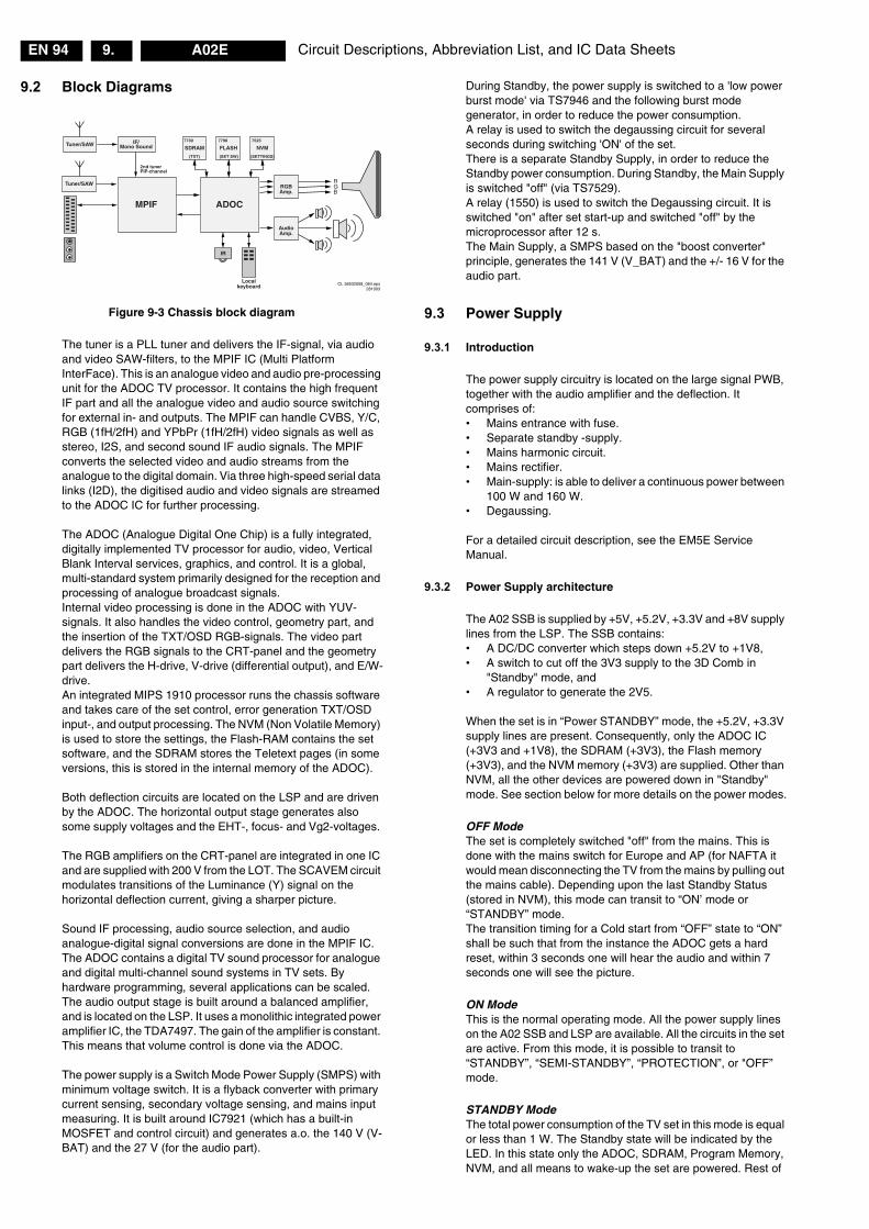
Circuit Descriptions, Abbreviation List, and IC Data SheetsEN 94 A02E9.
9.2 Block Diagrams
Figure 9-3 Chassis block diagram
The tuner is a PLL tuner and delivers the IF-signal, via audio and video SAW-filters, to the MPIF IC (Multi Platform InterFace). This is an analogue video and audio pre-processing unit for the ADOC TV processor. It contains the high frequent IF part and all the analogue video and audio source switching for external in- and outputs. The MPIF can handle CVBS, Y/C, RGB (1fH/2fH) and YPbPr (1fH/2fH) video signals as well as stereo, I2S, and second sound IF audio signals. The MPIF converts the selected video and audio streams from the analogue to the digital domain. Via three high-speed serial data links (I2D), the digitised audio and video signals are streamed to the ADOC IC for further processing. The ADOC (Analogue Digital One Chip) is a fully integrated, digitally implemented TV processor for audio, video, Vertical Blank Interval services, graphics, and control. It is a global, multi-standard system primarily designed for the reception and processing of analogue broadcast signals.Internal video processing is done in the ADOC with YUV-signals. It also handles the video control, geometry part, and the insertion of the TXT/OSD RGB-signals. The video part delivers the RGB signals to the CRT-panel and the geometry part delivers the H-drive, V-drive (differential output), and E/W-drive.An integrated MIPS 1910 processor runs the chassis software and takes care of the set control, error generation TXT/OSD input-, and output processing. The NVM (Non Volatile Memory) is used to store the settings, the Flash-RAM contains the set software, and the SDRAM stores the Teletext pages (in some versions, this is stored in the internal memory of the ADOC). Both deflection circuits are located on the LSP and are driven by the ADOC. The horizontal output stage generates also some supply voltages and the EHT-, focus- and Vg2-voltages. The RGB amplifiers on the CRT-panel are integrated in one IC and are supplied with 200 V from the LOT. The SCAVEM circuit modulates transitions of the Luminance (Y) signal on the horizontal deflection current, giving a sharper picture. Sound IF processing, audio source selection, and audio analogue-digital signal conversions are done in the MPIF IC. The ADOC contains a digital TV sound processor for analogue and digital multi-channel sound systems in TV sets. By hardware programming, several applications can be scaled.The audio output stage is built around a balanced amplifier, and is located on the LSP. It uses a monolithic integrated power amplifier IC, the TDA7497. The gain of the amplifier is constant. This means that volume control is done via the ADOC. The power supply is a Switch Mode Power Supply (SMPS) with minimum voltage switch. It is a flyback converter with primary current sensing, secondary voltage sensing, and mains input measuring. It is built around IC7921 (which has a built-in MOSFET and control circuit) and generates a.o. the 140 V (V-BAT) and the 27 V (for the audio part).
During Standby, the power supply is switched to a 'low power burst mode' via TS7946 and the following burst mode generator, in order to reduce the power consumption.A relay is used to switch the degaussing circuit for several seconds during switching 'ON' of the set.There is a separate Standby Supply, in order to reduce the Standby power consumption. During Standby, the Main Supply is switched "off" (via TS7529). A relay (1550) is used to switch the Degaussing circuit. It is switched "on" after set start-up and switched "off" by the microprocessor after 12 s.The Main Supply, a SMPS based on the "boost converter" principle, generates the 141 V (V_BAT) and the +/- 16 V for the audio part.
9.3 Power Supply
9.3.1 Introduction
The power supply circuitry is located on the large signal PWB, together with the audio amplifier and the deflection. It comprises of:• Mains entrance with fuse.• Separate standby -supply.• Mains harmonic circuit.• Mains rectifier.• Main-supply: is able to deliver a continuous power between
100 W and 160 W.• Degaussing. For a detailed circuit description, see the EM5E Service Manual.
9.3.2 Power Supply architecture
The A02 SSB is supplied by +5V, +5.2V, +3.3V and +8V supply lines from the LSP. The SSB contains:• A DC/DC converter which steps down +5.2V to +1V8,• A switch to cut off the 3V3 supply to the 3D Comb in
"Standby" mode, and • A regulator to generate the 2V5. When the set is in “Power STANDBY” mode, the +5.2V, +3.3V supply lines are present. Consequently, only the ADOC IC (+3V3 and +1V8), the SDRAM (+3V3), the Flash memory (+3V3), and the NVM memory (+3V3) are supplied. Other than NVM, all the other devices are powered down in "Standby" mode. See section below for more details on the power modes.
OFF Mode The set is completely switched "off" from the mains. This is done with the mains switch for Europe and AP (for NAFTA it would mean disconnecting the TV from the mains by pulling out the mains cable). Depending upon the last Standby Status (stored in NVM), this mode can transit to “ON’ mode or “STANDBY” mode.The transition timing for a Cold start from “OFF” state to “ON” shall be such that from the instance the ADOC gets a hard reset, within 3 seconds one will hear the audio and within 7 seconds one will see the picture.
ON Mode This is the normal operating mode. All the power supply lines on the A02 SSB and LSP are available. All the circuits in the set are active. From this mode, it is possible to transit to “STANDBY”, “SEMI-STANDBY”, “PROTECTION”, or "OFF” mode.
STANDBY ModeThe total power consumption of the TV set in this mode is equal or less than 1 W. The Standby state will be indicated by the LED. In this state only the ADOC, SDRAM, Program Memory, NVM, and all means to wake-up the set are powered. Rest of
Tuner/SAW
Tuner/SAW
IF/Mono Sound
MPIF ADOC
SDRAM
RGBAmp.
AudioAmp.
2nd tunerPIP-channel
FLASH
CL 36532058_064.eps281003
NVM
Localkeyboard
IR
7730
(TXT)
7790
(SET SW)
7525
(SETTINGS)
RGB

Circuit Descriptions, Abbreviation List, and IC Data Sheets EN 95A02E 9.
the A02 sub-systems are disconnected. This is controlled by a STANDBY control port.The transition timing from “STANDBY” to “ON” state is such that within 3 seconds, one will hear the audio and within 7 seconds, one will see the picture. From this mode, it is possible to transit to “ON”, “SEMI-STANDBY”, or “OFF” mode.
SEMI-STANDBY ModeAll the circuits in the set (ADOC, MPIF, etc), except the Audio output, Deflection, and hence CRT display, are powered up and fully active. The Audio Mute is activated. The set, however, will appear to behave and to look like “STANDBY” mode to the user. The user is totally oblivious of the existence of this mode.The status of the power supply lines and the estimated total power consumption of the SSB are the same as “ON” mode.In this mode, the ADOC ICs horizontal deflection drive output is disabled, while the STANDBY control port is disabled. This consequently causes the LOT stage on the LSP to be inactive (although V_batt voltage is present) that, in turn, will cause the EHT to be cut off. This in turn will cause the CRT display to be inactive.From this mode, it is possible to transit to “ON” mode, “STANDBY” mode, “PROTECTION” mode or “OFF” mode.
PROTECTION ModePower profile for protection mode is as low as required to allow “soft” diagnostics, error detection, and to indicate LED flashes to flag the type of fault. The horizontal deflection is "OFF" in this mode. From the protection mode, the only possible transition is to “OFF” mode.
9.3.3 Start Up Sequence
1. When we start the set (cold start), initially 5V2, 3V3, and 1V8 will be available. These come from the Standby module of the power supply.
2. After this, the microprocessor resets (tied to 1V8 and 3V3 supplies) and checks the last status of the supply from the NVM. Accordingly, the set will be put in STANDBY or in the normal ON condition.
3. Now, 5V and 8V are available if the last status was ON condition, and the DOP is initialised by the microcontroller through the PI bus (not via the I2C).
4. The H-drive will become available from the DOP, which is the source for the SUP_ENABLE signal.
5. Via the “SUP-ENABLE” signal, the Main Supply is switched “on” and will deliver the V_BAT to the Line deflection stage.
6. EHT generation is now started. 7. The uP will un-blank the picture.8. When you switch “off” the set, this is done in a controlled
way via the POR (Power On Reset) signal. Note: Standby is controlled by the STANDBY Line of the uP (not by the DOP).
9.3.4 Shut Down Sequence
This section describes the processes that need to be handled by hardware and software when power is disconnected from the set. Some system requirements:• To handle CRT discharge.• To handle "switch off" plops.• To prevent NVM corruption at switch "off".• To effectively distinguish between the condition of mains
interruptions and shutdown and handle them properly.• The "power down" detection is acquired from the deflection
supply (+11V) and the level is translated to +3.3V (this event has the highest interrupt priority to trigger SW shutdown procedure).
• Power down detection is fed to the FBCIN input, initiates a slow stop, and hence ensures CRT discharge (it is important that the slow-stop is maintained for at least 50 ms to assist good discharge).
• The microcontroller, hence the system, shall have a clean power "on" and power "off" reset with respect to its supply. The microcontroller shall not be operational when the supply voltage is below the recommended limits. The transition between active and reset is fast.
• The microcontroller "off" reset must occur much later (> 45 ms) than the POWER DOWN signal (P.DN).
When the POWER DOWN interrupt occurs, there is no way of knowing whether it is due to Medium Mains Interruptions or due to shutdown. Hence, there is no choice but to initiate shutdown procedure as described further below. The definition of Mains Interruption is given below:• Short Mains Interruptions. Duration of the interrupts <=
55 ms. The set shall continue to work properly. The "power off" acquisition circuit shall filter such events.
• Medium Mains Interruptions. Interruptions are of the order 70 to 80 ms. This is a typical situation when the "power off" acquisition circuit, signals that the power is going down but the microcontroller does not get a reset. In this condition, a POWER DOWN signal is generated but no POWER OFF RESET signal is available.
• Long Mains Interruption or Shutdown. Any interrupt above 80 ms shall cause a microcontroller reset and hence a cold start. This happens, when the power is disconnected long enough to get a "Power Off Reset" as well as the microcontroller reset. After this situation, the system would automatically cold start when the power resumes.
Figure 9-4 Shut down block diagram
Shutdown Procedure1. Exclude all processes and do not respond to any interrupts
- including RC events. However, during the following defined conditions of stopping the deflection (DFL-bit= 0), ignore the P.DN interrupt and rest of the procedure:– The system switched from ON to Standby by the user.– Protection event that forces the H-Deflection to stop.– Any other SW controlled event that causes the
deflection to stop.2. Since the P.DN signal is connected to FBCIN input, the
DOP shall slow stop immediately - no software intervention is required. The precondition for this is that the FBDM bit in DOP is set to "1". The slow -stop process will continue for the next 40 ms or so.
3. Mute Audio Output / Sound Enable line.4. Mute audio external outputs (in ADOC).5. Set the DFL-bit to "0", such that deflection shall not restart
after the slow -stop process is done.6. Disable NVM access. Do the following:
– Put the NVM in standby state to stop I2C write to NVM, by sending the Universal Reset Sequence.
– Set Write Enable high: this avoids any further Write sequence to the NVM.
7. Disable all the I2C hardware communication.
POWER-DOWNDETECTION
ADOC IC
FBCIN
POWER-DOWNInterrupt (P0_1|INT1)
+11V(LOT)
UP RESETGenerator
+5V2STANDBYSUPPLY
P.DN signal(POR_FLASH)
uP RESETSignal
RESET
CL 36532058_081.eps281003
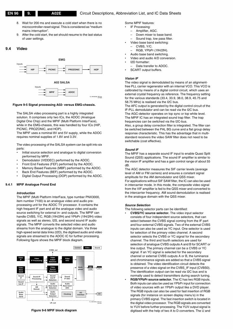
Circuit Descriptions, Abbreviation List, and IC Data SheetsEN 96 A02E9.
8. Wait for 200 ms and execute a cold start when there is no microcontroller-reset signal. This is considered as “medium mains interruption”.
9. After the cold start, the set should resume to the last status of user settings.
9.4 Video
Figure 9-5 Signal processing A02- versus EMG-chassis.
The SALSA video processing part is a highly integrated solution. It comprises only two ICs, the ADOC (Analogue Digital One Chip) and the MPIF (Multi Platform InterFace), while in the EMG-chassis, this was handled by four ICs (HIP, PICNIC, PROZONIC, and HOP). The MPIF uses a nominal 8V and 5V supply, while the ADOC requires nominal supplies of 1.8V and 3.3V. The video processing of the SALSA system can be spilt into six parts:• Initial source selection and analogue to digital conversion
performed by MPIF.• Demodulator (VIDDEC) performed by the ADOC.• Front End Features (FEF) performed by the ADOC.• Memory Based Features (MBF) performed by the ADOC.• Back End Features (BEF) performed by the ADOC.• Digital Output Processing (DOP) performed by the ADOC.
9.4.1 MPIF Analogue Frond End
IntroductionThe MPIF (Multi Platform InterFace, type number PNX3000, item number 7100) is an analogue video and audio pre-processing unit for the ADOC TV processor. It contains the high frequent IF part and all the analogue video and audio source switching for external in- and outputs. The MPIF can handle CVBS, Y/C, RGB (1fH/2fH) and YPbPr (1fH/2fH) video signals as well as stereo, I2S, and second sound IF audio signals. The MPIF converts the selected video and audio streams from the analogue to the digital domain. Via three high-speed serial data links (I2D), the digitised audio and video signals are streamed to the ADOC IC for further processing. Following figure shows the MPIF block diagram.
Figure 9-6 MPIF block diagram
Some MPIF features:• IF Processing:
– Amplifier, AGC.– Down mixer to base band.– Sound trap, low pass filter.
• Video base band switching:– CVBS, Y/C.– RGB, YPbPr (1fH/2fH).
• Audio base band switching.• Video and audio A/D conversion.• I2D formatter:
– Data transfer to ADOC.• SCART output buffers.
Vision IFThe video signal is demodulated by means of an alignment-free PLL carrier regenerator with an internal VCO. This VCO is calibrated by means of a digital control circuit, which uses an external crystal frequency as reference. The frequency setting for the various standards (33.4, 33.9, 38.0, 38.9, 45.75 and 58.75 MHz) is realised via the I2C bus. The AFC output is generated by the digital control circuit of the IF-PLL demodulator and can be read via the I2C bus. The AGC-detector operates on top sync or top white level. The MPIF IC has an integrated sound trap filter. The trap frequencies can be switched via the I2C-bus. Also, a group delay correction filter is integrated. The filter can be switched between the PAL BG curve and a flat group delay response characteristic. This has the advantage that in multi-standard receivers the video SAW filter does not need to be switchable (cost effective).
Sound IFThe MPIF has a separate sound IF input to enable Quasi Split Sound (QSS) applications. The sound IF amplifier is similar to the vision IF amplifier and has a gain control range of about 55 dB. The AGC detector measures the SIF carrier levels (average level of AM or FM carriers) and ensures a constant signal amplitude for the AM demodulator and QSS mixer.For applications without SIF SAW filter, the IC can also be used in intercarrier mode. In this mode, the composite video signal from the VIF amplifier is fed to the QSS mixer and converted to the intercarrier frequency. AM sound demodulation is realised in the analogue domain with the QSS mixer.
Source SelectionThe following selector parts can be identified:• CVBS/YC source selector. The video input selector
consists of four independent source selectors, that can select between the CVBS signal coming from the IF part and four external CVBS signals. Two of the external CVBS inputs can also be used as YC input. One selector is used for selection of the primary video channel. A second selector selects the CVBS or YC signal for the secondary channel. The third and fourth selectors are used for selection of analogue CVBS outputs A and B for SCART or line output. The primary channel can be a CVBS or YC signal. If an YC signal is selected for the secondary channel or external CVBS outputs A or B, the luminance and chrominance signals are added so that a CVBS signal is obtained. The video identification circuit detects the presence of a video signal on the CVBS_IF input (CVBS0). The identification output can be read via I2C bus and is normally used to detect transmitters during search tuning.
• RGB/YPbPr source selector. The IC has two RGB inputs. Both inputs can also be used as YPbPr input for connection of video sources with an YPbPr output like a DVD player. The RGB inputs can also be used for fast insertion of RGB signals (for instance on screen display menu’s) in the primary CVBS signal. The fast insertion switch is located in the digital video processor. The RGB signals are converted to YUV before further processing. The YUV output signal is digitised with the help of two A to D converters. The U and
HIP PICNIC
MPIF
A02 SALSA
EMG
ADOC
PROZONIC HOPHOP
CL 36532058_063.eps271003
Inputs
Inputs
VideoIF
VideoIF Processing
Sound IFProcessing
AMDemod.
Videooutput
Selection
CVBS_outControl Video Sound
VideoADC
VideoSource
Selection
Sound2nd IF
Selection
SoundIF ADC
AudioBase band
ADC
ClockingI2C
Interface
AudioBase bandSelection
AudioOutput
Selection
LR_out
VideoBaseband
SoundIF
Soundlow-IF
AudioBaseband
I2DLink
I2C
Multi-plexer
CL 36532058_065.eps281003
I2DI2D

Circuit Descriptions, Abbreviation List, and IC Data Sheets EN 97A02E 9.
V components have half the bandwidth of the Y signal, because the U and V signals are multiplexed and digitised with the help of one A to D converter.
Figure 9-7 MPIF Video source selection
• Audio source selectors. The MPIF contains two different audio source selectors. The first selector selects which audio signals are routed to the audio ADCs for further processing in the digital domain. The selector has two outputs, a primary channel and a secondary channel:– The primary audio channel is used for one stereo
signal. The secondary audio channel can carry a second stereo signal or AM sound signal.
– The second selector selects which audio signals are fed to the analogue audio outputs for SCART and line out. This selector has also two stereo inputs for demodulated sound signals coming from the digital video processor.
CL 36532058_073.eps071003
A
CVBS-IF
CVBS-1
CVBS-2
CVBS/Y-3
C3
CVBS/Y-4
C4
Y-COMB
C-COMB
R/Pr/V1
G/Y/Y-1
B/Pb/U1
R/Pr/V2
G/Y/Y-2
B/Pb/U2
+
YUV
RGB
Source
Switch
CLAMP LPF
DataLink
2
Yyuv
U
V
CLAMP
LPFCLAMP
A
D
LPFDataLink
1
A
D
DataLink
3
CVBS-outA
STROBE1N
STROBE1P
DATA1N
DATA1P
CVBS/Y prim
C prim
CVBS sec
Yyuv2Fh
SIFA/D
LR primDig
Yyuv2Fh
STROBE3N
STROBE3P
DATA3N
DATA3P
STROBE2N
STROBE2P
DATA2N
DATA2P
U,V
LPF
A
D
A
D
TimingCircuit
CLP primCLP sec
CLP Yyuv
CLP prim
CLP sec
CLP Yyuv
CVBS-SC1_AV1-IN
CVBS2_PIP_TUN2
Y-CVBS-SC2_AV2-IN
C-SC2_SVHS-IN
Y-CVBS-FRONT-IN
NT-IN
YOUT-COMB
COUT-COMB
R-SC1_V-IN
G-SC1-IN_Y-IN
B-SC1-IN_U-IN
7100-B
MPIF VIDEO SWITCH 19
60
61
63
62
50
51
53
54
55
56
57
58
46
45
123
126
9
8
5
4
1
15
16
25
26
27
30
31
32
5V49
64
STROBE1N
STROBE1P
DATA1N
DATA1P
STROBE3N
STROBE3P
DATA3N
DATA3P
STROBE2N
STROBE2P
DATA2N
DATA2P
HV_PRIM
HV_SEC
Mono Sec.Dig.
Ident
27/54 MHz
54MHz
54MHz
12CVBS-SC3 4152
CVBS-TERR
CVBS-DTV
HV-PRIM
HV-SECVCC-DIG
VCC-I2D
7062
CVBS-outB22
R-PR -2FH
G-Y-2FH
B-PB 2FH
7063
CVBS_SC2_MON_OUT
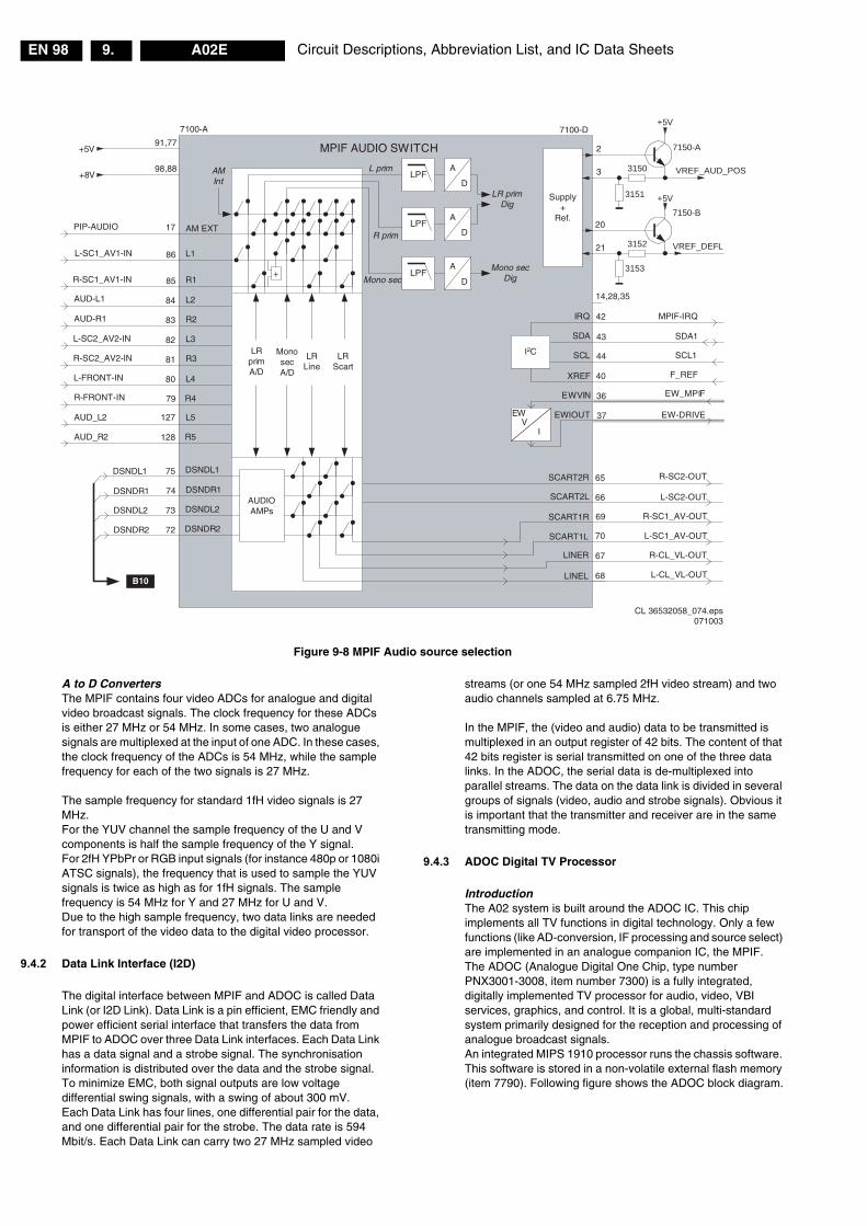
Circuit Descriptions, Abbreviation List, and IC Data SheetsEN 98 A02E9.
Figure 9-8 MPIF Audio source selection
A to D ConvertersThe MPIF contains four video ADCs for analogue and digital video broadcast signals. The clock frequency for these ADCs is either 27 MHz or 54 MHz. In some cases, two analogue signals are multiplexed at the input of one ADC. In these cases, the clock frequency of the ADCs is 54 MHz, while the sample frequency for each of the two signals is 27 MHz. The sample frequency for standard 1fH video signals is 27 MHz. For the YUV channel the sample frequency of the U and V components is half the sample frequency of the Y signal.For 2fH YPbPr or RGB input signals (for instance 480p or 1080i ATSC signals), the frequency that is used to sample the YUV signals is twice as high as for 1fH signals. The sample frequency is 54 MHz for Y and 27 MHz for U and V.Due to the high sample frequency, two data links are needed for transport of the video data to the digital video processor.
9.4.2 Data Link Interface (I2D)
The digital interface between MPIF and ADOC is called Data Link (or I2D Link). Data Link is a pin efficient, EMC friendly and power efficient serial interface that transfers the data from MPIF to ADOC over three Data Link interfaces. Each Data Link has a data signal and a strobe signal. The synchronisation information is distributed over the data and the strobe signal. To minimize EMC, both signal outputs are low voltage differential swing signals, with a swing of about 300 mV.Each Data Link has four lines, one differential pair for the data, and one differential pair for the strobe. The data rate is 594 Mbit/s. Each Data Link can carry two 27 MHz sampled video
streams (or one 54 MHz sampled 2fH video stream) and two audio channels sampled at 6.75 MHz. In the MPIF, the (video and audio) data to be transmitted is multiplexed in an output register of 42 bits. The content of that 42 bits register is serial transmitted on one of the three data links. In the ADOC, the serial data is de-multiplexed into parallel streams. The data on the data link is divided in several groups of signals (video, audio and strobe signals). Obvious it is important that the transmitter and receiver are in the same transmitting mode.
9.4.3 ADOC Digital TV Processor
IntroductionThe A02 system is built around the ADOC IC. This chip implements all TV functions in digital technology. Only a few functions (like AD-conversion, IF processing and source select) are implemented in an analogue companion IC, the MPIF.The ADOC (Analogue Digital One Chip, type number PNX3001-3008, item number 7300) is a fully integrated, digitally implemented TV processor for audio, video, VBI services, graphics, and control. It is a global, multi-standard system primarily designed for the reception and processing of analogue broadcast signals.An integrated MIPS 1910 processor runs the chassis software. This software is stored in a non-volatile external flash memory (item 7790). Following figure shows the ADOC block diagram.
CL 36532058_074.eps071003
+
LRprimA/D
MonosecA/D
LRLine
LRScart
AUDIOAMPs
LPFA
D
LPFA
D
LPFA
D
L prim
R prim
Mono sec
LR primDig
Mono secDig
AMInt
AM EXT
L1
R1
L2
R2
L3
R3
L4
R4
DSNDL1
DSNDR1
DSNDL2
DSNDR2SCART1L
SCART1R
LINER
LINEL
MPIF AUDIO SWITCH
69
70
67
68
PIP-AUDIO
L-SC1_AV1-IN
R-SC1_AV1-IN
L-SC2_AV2-IN
R-SC2_AV2-IN
AUD-R1
DSNDL1
DSNDR1
DSNDL2
DSNDR2
17
86
85
84
83
82
81
80
79
74
73
72
75
+5V91,77
98,88
R-SC1_AV-OUT
L-SC1_AV-OUT
L-CL_VL-OUT
R-CL_VL-OUT
L-SC2-OUT
R-SC2-OUT
43
44I2C
IRQ 42 MPIF-IRQ
EWV
I
EWVIN
EWIOUT
SCL
SDA
SCL1
SDA1
EW_MPIF
EW-DRIVE
F_REF
7100-A
XREF 40
36
37
Supply+
Ref.
2
3
20
21
B10
AUD-L1
7100-D
+8V
66
65SCART2R
SCART2L
L-FRONT-IN
R-FRONT-IN
AUD_L2
AUD_R2
L5
R5
127
128
14,28,35
7150-A
3151
3150
7150-B
3153
3152
+5V
+5V
VREF_AUD_POS
VREF_DEFL

Circuit Descriptions, Abbreviation List, and IC Data Sheets EN 99A02E 9.
Figure 9-9 ADOC block diagram
The dual stream architecture of the ADOC system allows audio and video processing of two A/V sources simultaneously. The two video streams can be displayed in several programmable ways (main screen, PIP or DW). The two audio streams are audible via the TV loudspeakers and/or the headphones. For the memory-based features (like scan rate conversion, 3D-Comb filtering, dynamic noise reduction, and PIP/DW applications), external SDRAM is used (item 7730). The ADOC also has 128 kBytes of internal SRAM memory. This memory is used to run low latency, timing critical parts of the software. The internal memory is also used if the system operates in a single scan 50/60 Hz interlace application without any other kind of memory based features. Under these circumstances, no external SDRAM is needed. Some ADOC features:• Video Decoding:
– 2-Colour Decoder (PAL, NTSC, SECAM).– 2D and 3D Comb filter.
• Memory Based Features:– PIP/DW, DNR, Scan Rate conversion.
• Picture Improvements:– CTI, LTI, Colour correction.
• Digital Output Processor:– RGB processing, Scavem, Deflection control.
• Audio Processing:– Demodulator/Decoder (A2, NICAM, BTSC).– Tone, Volume, Balance, Dolby ProLogic.
• VBI (Vertical Blank Interval) Services:– Teletext, Closed Caption, V-chip.
• TV Control:– I2C, UART, IR, Keyboard.
• Graphics:– Character based.
Video Decoding (VIDDEC)The Video Decoder (VIDDEC) is the video input processor and colour decoder. There are two VIDDECs: the primary and the secondary VIDDEC. The VIDDEC processes all CVBS, Y/C, and 1fH/2fH component (e.g. RGB) video input signals.
Figure 9-10 VIDDEC block diagram
Primary VIDDEC (1fH/2fH) The primary VIDDEC supports the following functionality:• Conversion of the digitised samples from MPIF into
orthogonal samples (meaning fixed number of pixels per line, independently of line frequency).
• Correction for any amplitude errors of the input signals (CVBS, YC, or YCbCr) by means of an Automatic Gain Control (AGC).
• Standard detection of PAL/NTSC or SECAM and various 1fH/2fH component input formats.
• Colour decoding for PAL, NTSC, or SECAM input signals.• Sync identification (to be used for channel search).• Sync processing for any 1fH or 2fH input signal.• Fast-blank insertion of RGB signals (supplied via MPIF) on
CVBS input signals.• 2D Comb filtering. 3D Comb filtering is implemented in the
Memory Based Feature block of the Feature Box.
Secondary VIDDEC (1fH)The secondary VIDDEC is mainly intended for use with PIP/DW. It supports the following functionality:• Conversion of the digitised samples from MPIF into
orthogonal samples (meaning fixed number of pixels per line, independently of line frequency).
• Correction for any amplitude errors of the input signals (CVBS) by means of an Automatic Gain Control (AGC).
• Standard detection of PAL/NTSC or SECAM and various 1fH component input formats.
• Colour decoding for PAL, NTSC, or SECAM input signals.• Sync identification (to be used for channel search).• Sync processing for any 1fH input signal.• CVBS 1fH input signals only.
Data Synchroniser and Sample Rate ConverterThe data synchroniser is a de-multiplexer that separates the UV stream into a separate U and V data stream. The sample rate converter converts the video samples from the crystal clock domain to the so-called line locked clock domain, 720 pixels per line.
Automatic Gain Control (AGC)The AGC amplifier block controls the gain of the signal and is controlled directly by the chassis software. This gain will depend on the amplitude of the output signal (signal amplitude and/or sync amplitude) as measured by the AGC gain block. As a secondary function, it controls both the offset at the input and the offset at the output of the gain control.
Digital Multi Standard Decoder (DMSD)This DMSD block contains the following functionality:
Video
Primarycolour
decoder
Secondary
colourdecoder
MainSub
select
FrontEnd
Features
Memorybased
Features
BackEnd
Features
DigitalOutput
Processor
CL 36532058_066.eps281003
Control Sound
L/R/HP/MON/...
SDRAM
I2S ROM/FLASH/SRAM
RGB
Defl.
SDRAMMMI
128KBSRAM
MemoryMIPS
PR1910Graphics
EBIUInterface
Peripherals
SOUNDDem.
SOUNDDec.
(DSP)
SOUNDSwitch
AUDIOFeatures
(DSP)
DAC
I2DLink
STROBE1N
STROBE1P
DATA1N
DATA1P
STROBE3N
STROBE3P
DATA3N
DATA3P
STROBE2N
STROBE2P
DATA2N
DATA2P
HV_PRIM
HV_SEC
I2D1
I2D3
I2D2FAST-BLANK
FIFO
DMSD
CHR.MUX
DE-MUX
FASTBLANK
SWITCH
FOR-MATER
SYNC2Fh
HVINFO
HVSYNC
ADOC VIDDEC (PRI & SEC)
7300-J
DA
TA
SY
NC
SA
MP
LE R
AT
E C
ON
VE
RTE
R
AG
C_A
MP
PRI
SEC
SSIF
VIDDEC1
VIDDEC2
ExtSyn
cMux
SRC forHFB1/H-Sync
SyncMux.
H-2FH
V-2FH
FBL-SC1-IN
VDDCO VDDE
EXT. STEREO
EXT. MONO
DLI
NK
-VD
DA
DLI
NK
-VD
DD
VID
1-D
TC
-VD
DA
PLL
VD
DA
VID
1-D
TC
-VD
D3
B6
B8
DMSD=Digital Multi Standard Decoder
CL 36532058_067.eps281003
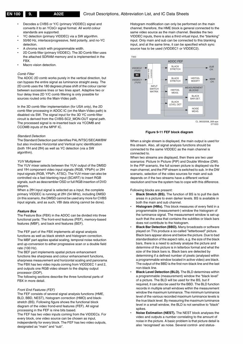
Circuit Descriptions, Abbreviation List, and IC Data SheetsEN 100 A02E9.
• Decodes a CVBS or Y/C (primary VIDDEC) signal and converts it to an YCbCr signal format. All world colour standards are supported.
• YC detection (primary VIDDEC) via a SW algorithm.• 50/60 Hz, interlace/progressive, field polarity, and no-YC
detection.• A chroma notch with programmable width.• 2D Comb filter (primary VIDDEC). The 3D Comb filter uses
the attached SDRAM memory and is implemented in the FBX.
• Macro vision detection.
Comb FilterThe ADOC 2D comb works purely in the vertical direction, but can bypass the entire signal as luminance straight away. The 2D comb uses the 180 degrees phase shift of the colour carrier between successive lines or two lines apart. Adaptive two or four delay lines 2D Y/C comb filtering is only possible for sources routed onto the Main-Video path. In the 3D comb filter implementation (for USA only), the 2D comb filter processing in ADOC IC (on the Main-Video path) is disabled via SW. The signal input for the 3D YC comb-filter circuit is derived from the CVBS-SC2_MON-OUT signal path. The processed signal is re-inserted back via YCOMB and CCOMB inputs of the MPIF IC.
Standard DetectionThe Standard Detection part identifies PAL/NTSC/SECAM/BW but also involves Horizontal and Vertical sync identification (both 1fH and 2fH) as well as YC detection (via a SW algorithm).
YUV MultiplexerThe YUV mixer selects between the YUV output of the DMSD and 1fH component video input signals (RGB, YPbPr) or 2fH input signals (RGB, YPbPr, ATSC). The YUV mixer can also be controlled via a fast blanking input (SCART) to insert RGB signals, such as descrambler OSD or full RGB insertion of DVD players.When a 2fH input signal is selected as a input, the complete primary VIDDEC is running at 2fH (54 MHz), including DMSD (in this scenario, the DMSD cannot be used any more for CVBS input signals, and as such, VBI data slicing cannot be done).
Feature BoxThe Feature Box (FBX) in the ADOC can be divided into three functional parts: The front-end features (FEF), memory-based features (MBF), and back end features (BEF). The FEF part of the FBX implements all signal analysis functions as well as black stretch and histogram correction. The MBF part applies spatial scaling, temporal noise reduction and up-conversion to either progressive scan or a double field rate (100 Hz). The BEF part implements spatial picture enhancement functions like sharpness and colour enhancement functions, sharpness measurement and horizontal scaling and panoramaThe FBX has two video inputs coming from VIDDDEC 1 and 2, and outputs one RGB video stream to the display output processor (DOP).The following sections describe the three functional parts of FBX in more detail.
Front End Features (FEF)The FEF consists of several signal analysis functions (HME, BLD, BBD, NEST), histogram correction (HMO) and black-stretch (BS). Following figure shows the functional block diagram of the video frond-end features (FEF). All signal processing in the FEF is nine bits based.The FEF has two video inputs coming from the VIDDECs. For every block, one video source can be chosen as input, independently for every block. The FEF has two video outputs, designated as “main” and “sub”.
Histogram modification can only be performed on the main channel; therefore, the HME block is general connected to the same video source as the main channel. Besides the two VIDDEC inputs, there is also a third virtual input, the “blanking” input. Only main and sub can be connected to this blanking input, and at the same time, it can be specified which sync source has to be used (VIDDEC1 or VIDDEC2).
Figure 9-11 FEF block diagram
When a single stream is displayed, the main output is used for this stream. Also, all signal analysis functions should be connected to the same VIDDEC as the main channel is connected to.When two streams are displayed, then there are two user scenarios: Picture In Picture (PIP) and Double Window (DW). In the PIP scenario, the full screen picture is displayed via the main channel, and the PIP stream is switched to sub. In the DW scenario, selection of the video sources for main and sub depends on if the two streams have a different vertical resolution and how the system has to cope with this difference. Following blocks are present:• Black Stretch (BS). The function of BS is to pull the dark
areas in a picture to even darker levels. BS is available in both the main and sub channel.
• Histogram (HMx). This block measures of every field in a programmable (measurement-) window the histogram of the luminance signal. The measurement window is set-up such that the area that contains the subtitles or black bars does not contribute to the histogram.
• Black Bar Detection (BBD). Many broadcasts or software played on TVs produce a so-called "letterboxed" picture. Black bars appear above and below the picture. Due to bad standardisation of the aspect ratio, e.g. the size of the black bars, there is a need to actively analyse the picture and determine of the picture is in letterbox format and what the size of the black bars is. Black bars are detected by determining if a defined number of pixels (analysed within a programmable window located in active video) are black. The output of the BBD is the first non-black line and the last non-black line.
• Black Level Detection (BLD). The BLD determines within a programmable (measurement) window the “black level” of a picture. The BLD will be used for the BS, but if required, it can also be used for the BBD. The BLD function records in multiple small windows within the measurement window the maximum luminance. The minimum luminance level of the various recorded maximum luminance levels is the true black level. By measuring the maximum luminance level in a small window, the BLD is not sensitive to “black” spikes.
• Noise Estimation (NEST). The NEST block analyses the video and outputs a number correlating to the amount of noise in the picture. A basic problem is that picture detail is also ‘recognised’ as noise. Several control- and status-
CL 36532058_069.eps071003
INPUTSWITCHMATRIX
BLACKSTRETCH
BLACKSTRETCH
HISTOG.MODIFY
HISTOG.MEAS.
BLACKBAR DET.
BLACKLEVEL DET
NOISEMEAS.
MEASUREMENTBLOCKS
VIDDEC1
VIDDEC2
MAINCH.
SUBCH.
ADOC FEF
(YUV)
(YUV)
SA
MP
LE R
ATE
CO
NV
ER
TER
B5
7300
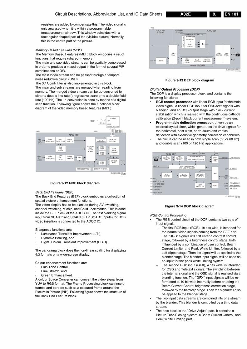
Circuit Descriptions, Abbreviation List, and IC Data Sheets EN 101A02E 9.
registers are added to compensate this. The video signal is only analysed when it is within a programmable (measurement) window. This window coincides with a rectangular shaped part of the (visible) picture. Normally this is the centre part of the picture.
Memory Based Features (MBF)The Memory Based Features (MBF) block embodies a set of functions that require (shared) memory. The main and sub video streams can be spatially compressed in order to produce a mixed output in the form of several PIP combinations or DW. The main video stream can be passed through a temporal noise reduction circuit (DNR). The 3D Comb filter is also implemented in this block. The main and sub streams are merged when reading from memory. The merged video stream can be up-converted to either a double line rate (progressive scan) or to a double field rate (100 Hz). The up-conversion is done by means of a digital scan function. Following figure shows the functional block diagram of the video memory based features (MBF).
Figure 9-12 MBF block diagram
Back End Features (BEF)The Back End Features (BEF) block embodies a collection of spatial picture enhancement functions. The video display has to be blanked during AV switching, channel switching, V-chip, and Child Lock modes. This is done inside the BEF block of the ADOC IC. The fast blanking signal input from SCART1and SCART3 (TV SCART inputs) for RGB video insertion is connected to the ADOC IC. Sharpness functions are:• Luminance Transient Improvement (LTI), • Dynamic Peaking, and • Digital Colour Transient Improvement (DCTI). The panorama block does the non-linear scaling for displaying 4:3 formats on a wide-screen display. Colour enhancement functions are:• Skin Tone Control, • Blue Stretch, and • Green Enhancement. A colour Space Converter can convert the video signal from YUV to RGB format. The Frame Processing block can insert frames and borders such as a coloured frame around the Picture in Picture (PIP). Following figure shows the structure of the Back End Feature block.
Figure 9-13 BEF block diagram
Digital Output Processor (DOP)The DOP is a display processor block, and contains the following functions:• RGB control processor with linear RGB input for the main
video signal, a linear RGB input for OSD/text signals with blending, and an RGB output stage with black current stabilisation which is realised with the continuous cathode calibration (2-point black current measurement) system.
• Programmable deflection processor, driven by an external crystal clock, which generates the drive signals for the horizontal, east-west, north-south and vertical deflection with extensive geometry correction capabilities.
• The circuit can be used in both single scan (50 or 60 Hz) and double scan (100 or 120 Hz) applications.
Figure 9-14 DOP block diagram
RGB Control Processing• The RGB control circuit of the DOP contains two sets of
input signals:– The first RGB input (RGB), 10 bits wide, is intended for
the normal video signals coming from the BEF part. The "RGB" signals will first enter a contrast control stage, followed by a brightness control stage, both influenced by a combination of user control, Beam Current Limiter and Peak White Limiter, followed by a soft clipper stage. Then the signal will be applied to the blender stage. The blender input signal will be used as an input for the peak white limiting system.
– The second RGB input (GFX), 4 bits wide, is intended for OSD and Teletext signals. The switching between the internal signal and the OSD signal is realised via a blending function. The "GFX" input signals will be re-formatted to 10 bit wide internally before entering the Beam Current Control brightness correction stage, followed by the hard clip stage. Then the signal will also be applied to the blender stage.
• The two input data streams are combined into one stream by the blender. This blender is controlled by a third data stream.
• The next block is the "Drive Adjust" part. It contains a Picture Tube Biasing system, a Beam Current Control, and Peak White Limiting part.
CL 36532058_070.eps071003
HOR.COMPRESS
HOR.COMPRESS
MAINCH.
SUBCH.
VERT.COMPRESS
SUBFIFO
CACHE
NOISESHAPER
MAINFIFO
CACHE
NOISESHAPER
DNR
MEMORYBUS
DEVICEINTERF.
UNDI-THER
UNDI-THER
SCANRATE
CONVERT
OUTPUTMUX.UNDI-
THER
DISPLAY CONTROLMODE CONTROL
SDRAM
ADOC MBF
Y
UV
7730
(YUV)
(YUV)
1,14,27
3,9,43,49VDDE
7300-I
VDD
VDDQ
FIELD MEMORY & TXT PG
MEMORYCTRL/SWI.
MM
I BU
S SA0...SA11SD0...SD15
DTL I/F
7300
CL 36532058_071.eps071003
SKINTONE
CONTROL
BLUESTRETCH
GREENENHANCE
RGBMATRIX
FRAMEPROC.
PANO-RAMA
DCTI
SHARPNESS
MEASURE
LTI
DYN.PEAKING
FILTER
LUMINANCE SHARPNESS
COLOUR FEATURES
Y
UV
Y
U
V
U
V
Y Y
U
V
R
G
B
ADOC BEF13.5 / 27 MHz@ 720 ppl
27 / 54 MHz@ 1440 ppl
B7TO
7300
CL 36532058_068.eps071003
Hor. TIMEBASE GEN.DTO & CONTROL LOOP
SLOW START/STOP
L0W POWER STARTUP
1stCONTROL
LOOP
SDAC
HIRES.TIMINGGEN.
HOR. TIMEBASE GEN.DTO & CONTROL LOOP
SLOW START/STOP
L0W POWER STARTUP
1stCONTROL
LOOP
SDAC
HIRES.TIMINGGEN.
ADC
2ndCONTROL
LOOP
VERT.WAVEFORM
EAST-WESTWAVEFORM
VERT.SAWTOOTH
VERT.DRIVER
HDROUT LINE DRIVERS
EHT INFO
POR FLASH
FRAME DRIVE+
FRAME DRIVE -
EW-DRIVE
HFB
EHT
BCL
FBCIN
EWP
VDRP
VDRN
ADOC DOP
HVSYNC
FLASHX-PROT
BPA
SDAC-VDDA
DOP-DTC-VDDA
DOP-DTC-VDD3
IMEAS-VDDA
SDAC-3V3
B5
SEL2FH
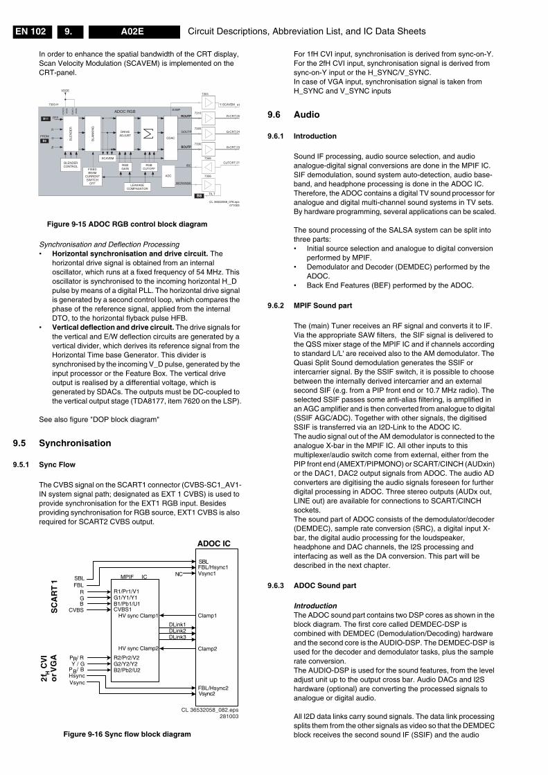
Circuit Descriptions, Abbreviation List, and IC Data SheetsEN 102 A02E9.
In order to enhance the spatial bandwidth of the CRT display, Scan Velocity Modulation (SCAVEM) is implemented on the CRT-panel.
Figure 9-15 ADOC RGB control block diagram
Synchronisation and Deflection Processing• Horizontal synchronisation and drive circuit. The
horizontal drive signal is obtained from an internal oscillator, which runs at a fixed frequency of 54 MHz. This oscillator is synchronised to the incoming horizontal H_D pulse by means of a digital PLL. The horizontal drive signal is generated by a second control loop, which compares the phase of the reference signal, applied from the internal DTO, to the horizontal flyback pulse HFB.
• Vertical deflection and drive circuit. The drive signals for the vertical and E/W deflection circuits are generated by a vertical divider, which derives its reference signal from the Horizontal Time base Generator. This divider is synchronised by the incoming V_D pulse, generated by the input processor or the Feature Box. The vertical drive output is realised by a differential voltage, which is generated by SDACs. The outputs must be DC-coupled to the vertical output stage (TDA8177, item 7620 on the LSP).
See also figure "DOP block diagram"
9.5 Synchronisation
9.5.1 Sync Flow
The CVBS signal on the SCART1 connector (CVBS-SC1_AV1-IN system signal path; designated as EXT 1 CVBS) is used to provide synchronisation for the EXT1 RGB input. Besides providing synchronisation for RGB source, EXT1 CVBS is also required for SCART2 CVBS output.
Figure 9-16 Sync flow block diagram
For 1fH CVI input, synchronisation is derived from sync-on-Y. For the 2fH CVI input, synchronisation signal is derived from sync-on-Y input or the H_SYNC/V_SYNC. In case of VGA input, synchronisation signal is taken from H_SYNC and V_SYNC inputs
9.6 Audio
9.6.1 Introduction
Sound IF processing, audio source selection, and audio analogue-digital signal conversions are done in the MPIF IC. SIF demodulation, sound system auto-detection, audio base-band, and headphone processing is done in the ADOC IC. Therefore, the ADOC contains a digital TV sound processor for analogue and digital multi-channel sound systems in TV sets. By hardware programming, several applications can be scaled. The sound processing of the SALSA system can be split into three parts:• Initial source selection and analogue to digital conversion
performed by MPIF.• Demodulator and Decoder (DEMDEC) performed by the
ADOC.• Back End Features (BEF) performed by the ADOC.
9.6.2 MPIF Sound part
The (main) Tuner receives an RF signal and converts it to IF. Via the appropriate SAW filters, the SIF signal is delivered to the QSS mixer stage of the MPIF IC and if channels according to standard L/L' are received also to the AM demodulator. The Quasi Split Sound demodulation generates the SSIF or intercarrier signal. By the SSIF switch, it is possible to choose between the internally derived intercarrier and an external second SIF (e.g. from a PIP front end or 10.7 MHz radio). The selected SSIF passes some anti-alias filtering, is amplified in an AGC amplifier and is then converted from analogue to digital (SSIF AGC/ADC). Together with other signals, the digitised SSIF is transferred via an I2D-Link to the ADOC IC.The audio signal out of the AM demodulator is connected to the analogue X-bar in the MPIF IC. All other inputs to this multiplexer/audio switch come from external, either from the PIP front end (AMEXT/PIPMONO) or SCART/CINCH (AUDxin) or the DAC1, DAC2 output signals from ADOC. The audio AD converters are digitising the audio signals foreseen for further digital processing in ADOC. Three stereo outputs (AUDx out, LINE out) are available for connections to SCART/CINCH sockets.The sound part of ADOC consists of the demodulator/decoder (DEMDEC), sample rate conversion (SRC), a digital input X-bar, the digital audio processing for the loudspeaker, headphone and DAC channels, the I2S processing and interfacing as well as the DA conversion. This part will be described in the next chapter.
9.6.3 ADOC Sound part
IntroductionThe ADOC sound part contains two DSP cores as shown in the block diagram. The first core called DEMDEC-DSP is combined with DEMDEC (Demodulation/Decoding) hardware and the second core is the AUDIO-DSP. The DEMDEC-DSP is used for the decoder and demodulator tasks, plus the sample rate conversion.The AUDIO-DSP is used for the sound features, from the level adjust unit up to the output cross bar. Audio DACs and I2S hardware (optional) are converting the processed signals to analogue or digital audio. All I2D data links carry sound signals. The data link processing splits them from the other signals as video so that the DEMDEC block receives the second sound IF (SSIF) and the audio
CL 36532058_076.eps071003
DRIVEADJUST
CDAC
BLENDERCONTROL
ADC
LEAKAGECOMPASATOR
7310
7330
R-CRT
G-CRT
B-CRT
CUTOFF
ROUTP
GOUTP
BOUTP
DRIVEADJUST
CDAC
RGBCUTOFF
RGBGAIN
BLENDERCONTROL
ADC
LEAKAGECOMPASATOR
FIXEDBEAM
CURRENTSWITCH
OFF
GFX ROUTP
BOUTP
IBC
IBCRANGE
ADOC RGB
7300-H
R
G
B
7320
41
25
24
23
21
VDDE
FROM
B6
B11
CD
AC
2-
VD
DA
CD
AC
1-
VD
DA
Y-SCAVEM
BLE
ND
ER
BLA
NK
ING
SCAVEM
SVMP
7346
7356
TILTB8
7304
RGB
FBL
PR / RY / G
PB / BHsyncVsync
NCFBL/Hsync1
FBL/Hsync2
Vsync1
Vsync2
Clamp1
Clamp2
HV sync Clamp1
HV sync Clamp2
G1/Y1/Y1B1/Pb1/U1
R1/Pr1/V1
G2/Y2/Y2B2/Pb2/U2
R2/Pr2/V2
CVBS CVBS1
DLink1DLink2DLink3
SC
AR
T 1
2f H
CV
Io
r VG
A
MPIF IC
ADOC IC
SBL
SBL
CL 36532058_082.eps281003
Circuit Descriptions, Abbreviation List, and IC Data Sheets EN 103A02E 9.
signals from the audio ADCs of the MPIF IC. The SSIF needs some hardware processing before it enters the DEMDEC DSP. The DEMDEC processing will be described in the next chapter.The audio signals from the audio ADCs of the MPIF are passing the DEMDEC DSP only for source selection and sample rate conversion.In this chassis, two of the DAC outputs are used to feed a headphone. Two other DAC stereo outputs are provided for the audio feedback to the MPIF IC. They are located to pins of the ADOC that suit best for connection to MPIF.
Figure 9-17 ADOC sound processing block diagram
DEMDEC DSPThe output signals of the above-mentioned hardware blocks, plus four audio ADC channels are read in by the DEMDEC DSP, processed, converted to the current audio sample rate, “demultiplexed”, and forwarded to the Audio DSP for further processing (volume, tone control, effects etc.).
Down MixerThe digitised SSIF input signal is fed to the mixers, which mix one or both input sound carriers down to zero IF.
Pre-processingThis part contains the sound system identification and demodulation circuitry.
Audio Sample Rate Conversion (SRC)All input signals pass through a sample rate conversion to the actual output sample rate (usually 48 kHz) such that the output rate does not need to be synchronised with any of the input rates. Up to five separate channels can be converted.
Audio Processing DSPThis block applies several filters, like down-sampling and de-emphasis, noise reduction processing, performs a sample rate conversion (SRC) to the current audio sample rate, and routes the decoded signals to the output channels. The generic processing controls are Volume, Bass, Treble, Balance, Incredible Surround, Spatial (incredible mono), DBE, Dynamic Ultra Bass II (for non-woofer sets only), AVL, Sub-Woofer, and 5-band Graphic equaliser.The Headphone volume can be separately controlled in the Headphone menu without affecting the master volume (the setting of the volume tables will be adapted after fine tuning).For variable volume output for USA, the DAC1 output will switch to the Main channel and therefore the same volume curve for the Main Channel can be used.
9.6.4 Audio Amplifier
Speakers (diagram A6)The audio output stage is built around IC7701 , which is a balanced amplifier, and is located on the LSP. It uses an monolithic integrated power amplifier IC, the TDA7497. The gain of the amplifier is constant. This means that volume control is done via the ADOC.The supply voltage is +28 V, generated by the power supply via L5506 (or L5512). The TDA7497 delivers an output of 3 x 10 W_rms to two full range speakers and an (optional) subwoofer.
MutingThere are three types of muting available: system mute, headphone status mute, and user mute.• System mute. System muting is implemented for “special
events” such as channel/source change event, loss of identification signal, "on/off" switching of the set, during search and auto store/program, and/or sound mode change. This muting is transparent to the user. Audio output is muted before the above “special events” occurred, to prevent problems such as audible plop. Muting is done via the SOUND-ENABLE (software controlled) and/or POR (hardware controlled) line connected (via TS7710 and 7711) to pin 10 of the amplifier-IC and coming from the ADOC microprocessor.
• Headphone status mute. A headphone status is available to detect the presence of the headphone and mute the main speakers if the headphone is detected. The microprocessor will read the FRONT-DETECT status.
• User mute. This is a mute option available to the user. The user select the MUTE option on the remote control to switch "off/on" the sound output to the main loudspeaker and the (optional) subwoofer.
Headphone amplifier (diagram A7)The headphone amplifier is built around IC7751 (NJM4556), which is a high-gain, high output current dual operational amplifier. The supply voltage is +5 V.
9.7 Control
9.7.1 Introduction
The MIPS processor within the ADOC performs the control of the complete SALSA system. This part of the document will examine the functions that enable the MIPS to operate and control the remainder of the SALSA system. Some control features: • MIPS1910 processor (MIPS).• Embedded SRAM.• External Bus Interface Unit (EBIU) for external memory
access.• SDRAM Interface.• Interrupt Controller.• Power and Clock management.• General Purpose I/O (GPIO).• Analogue to Digital conversion.• Two x I2C master/slave.• Two x General Purpose Timers.• UART.• Two x Multi-standard VBI Data Capture Unit.• EJTAG (for debug and boundary scan functions).• Remote Control (Infra Red) pre-processing.• Graphics.
CL 36532058_077.eps281003
DAC
DDEP
DownMix
Preprocessing SRCDematrix
and Select
LevelAdj.
I/PX-
Bar
I2SOUT
O/PX-
Bar
Noi
se S
hape
r
Demodulation and Decoding DSP
AUD_SPK_SW
AUD_SPK_R
AUD_SPK_L
AUD_SPK_C
AUD_SPK_SL
AUD_HP_R
AUD_HP_L
DSNDL1
DSNDR1
DSNDL2
DSNDR2
SSIF
ADOC SOUND & AUDIO PROCESSING
VDDCO VDDE
EXT. STEREO
EXT. MONO
7300-x
7300-B
B5
SD
AC
1-V
DD
A
SD
AC
1-3V
3
DecimationFilter
I2SIN
WS PLL
Audio Processing DSP
SD
I
SC
KI
WS
I
SD
02
SC
K02
WS
02
N.C. N.C.
Circuit Descriptions, Abbreviation List, and IC Data SheetsEN 104 A02E9.
Figure 9-18 ADOC control block diagram
9.7.2 Internal Bus Structure
PI BusThe Peripheral Interconnect (PI) bus connects all of the functional blocks within the ADOC device. Physically it is split into four distinct sections. These are referred to as:• Fast PI Bus.• Slow PI Bus.• Video PI Bus.• Sound PI Bus.The individual segments of the PI bus are interconnected via PI-PI bridges. When several devices are connected to a bus system section only one of these may have control (ownership) of the bus section at any instant in time. The device that has control is referred to as the bus master, the remaining devices are referred to as slaves. Each bus segment section has a Bus Control Unit (BCU), which allocates bus ownership to the various modules that are capable of being bus masters. A bus master may have ownership of one or more sections of the PI bus.
Extension Bus Interface UnitThe Extension Bus Interface Unit (EBIU) allows various types of memory (ROM/FLASH/SRAM) to be attached to the ADOC IC and must therefore be configured per memory type (in terms of chip select lines, bus width used, and access times). This enables the hardware of the EBIU to correctly address the external memories and apply the correct number of wait states.
9.7.3 Microprocessor Reset
The reset of the device is split between three functions:
• Power-On-Reset (POR). Output is fed to the Power Clock Reset (PCR) block generating a Hard reset (all functions reset).
• PCR. In simplified terms two outputs are available:– Hard reset, all blocks within ADOC are reset.– Soft reset, a limited number of blocks within the control
core are reset.• GP registers are used to allow software control of the reset
to certain blocks within ADOC.
9.7.4 External Bus Structure
I2C BusThe system has two system I2C buses; one for the devices on the SSB and the other for the devices used in the external modules .• The I2C-1 system bus, comprises of SCL and SDA, is used
to control all the I2C devices on the LSP (the main tuner) and other I2C devices connected to other external panels (PIP Front-End demodulation IC, PIP tuner, etc.). The I2C-1 is a 100 kHz bus and is called as "slow" bus. It is connected to the +5V supply. All these devices are powered down in the Standby mode.
• The I2C-2 system bus, comprises of SCL2 and SDA2, is used to control all the I2C devices (MPIF, 3D-Comb, NVM, etc.) present on the SSB. The I2C-2 is a 400 kHz bus and is called as "fast" bus. It is connected to the +3.3V supply.
9.8 Protections
For a detailed description, see chapter 5 "Service Modes, Error Codes, and Fault Finding".
9.9 Software Upgrading
In this chassis, you can upgrade the software via ComPair. This offers the possibility, to replace the entire SW image without having to remove the flash-RAM from its socket. You can find more information on how this procedure works in the ComPair file. It is possible that not all sets are equipped with the hardware, needed to make software upgrading possible. To speed up the programming process, the firmware of the ComPair interface can be upgraded. See Chapter "Service Modes ..."; paragraph "ComPair" - “How To Order” for the order number.
CL 36532058_075.eps071003
MIPS EBIU
SRAM128KB
PI-PIBRIDGE
GFXGEN
GPIO
I2C
A/DADC
TIMER
GFX
FAST PI_BUS
SLOW PI_BUS
1581
2582
2581
KEYBOARD
FRONT-DETECT
STATUS1_PIP-AFT-50-60HZ
SEL-SHVS-RR_STATUS2
LIGHT-SENSOR
RC5
SDA0
SCL0
SDA1
SCL1
SEL-IF-LL
SOUND-ENABLE
SEL-2FH-SRC_STATUS3
DEGAUSS
STANDBY
MPIF-IRQ
W
E
G
VDDE7790
SEL-2FH-SRC_STATUS3
DTV_EXPENSION
COMM_LINE (SCART)
F_REF
ADOC-uP & CONTROL
POR_FLASHB8
B18
B4
B1
B4
(FROM 0223)
B18
7300-A,C,E & K
ADC1
ADC4
P2-6
P3-0
ADC3
ADC0
ADC5
P0-7
P0-3
P0-1
P3-2
P0-6
P0-4
P2-4
P2-2
P0-5
P1-1
P1-0
P1-3
P1-2
MPIFCLK
XOUT
XIN
(SCART)
FOR 2FH I/P or SCART-3
BUS
A1.
.A21
D0.
.D15
VDD
MEMORY INTERFACE
B7
9,37
VDDQ43
FLASH
RESET_
FLASH_RST
POR_FLASH
FLASH_RST16RP
ADC2
VDDE
VDDCO
ADC-VDDA
XVDD
5570
5583
7525
WC_
5
6
7
VDDE
8
P1-5
SCL
SDA NVM
VPP
SDM
4565
4564
RES
SYSTEMRESET(50ms)
7581
VDDE
+5V2
3582
3590
3583
3586
1
5
4
15
RB
RB
RB53
P0-2
Circuit Descriptions, Abbreviation List, and IC Data Sheets EN 105A02E 9.
9.10 Abbreviation list
Table 9-1 Abbreviations
Abbreviation Description
0/6/12 SCART switch control signal on A/V board. 0 = loop through (AUX to TV), 6 = play 16:9 format, 12 = play 4:3 format
2CS 2 Carrier Stereo
A2 Commonly known as two carriers sound (2CS) system
AC (or ac) Alternating Current
ACI Automatic Channel Installation: algorithm that installs TV channels directly from a cable network by means of a predefined TXT page
ADC Analogue to Digital Converter
ADOC Analogue Digital One Chip
AFC Automatic Frequency Control: control signal used to tune to the correct frequency
AGC Automatic gain control (feedback) signal to the tuner.
AM Amplitude Modulation
ANR Automatic Noise Reduction: one of the algorithms of Auto TV
AP / A/P Asia Pacific
AR Aspect Ratio: 4 by 3 or 16 by 9
ASD Automatic Standard Detection
AV External Audio Video
AVL Automatic Volume Level control
B Blue
B/G Monochrome TV system. Sound carrier distance is 5.5 MHz
BBD Black Bar Detection
BCL Beam Current Limiter
BC-PROT PROTection signal to the microprocessor for a too high Beam Current.
BG System B and G
BLC-INFO BLack Current INFO
BLD Black Level Detection
BS Black Stretch
BTSC Broadcast Television Standard Committee. Multiplex FM stereo sound system, originating from the USA and used e.g. in LATAM and AP-NTSC countries
C Chroma (video) / Centre channel (audio)
CL Constant Level: audio output to connect with an external amplifier
CLUT Colour Look Up Table
ComPair Computer aided rePair
CRT Cathode Ray Tube or picture tube
CSM Customer Service Mode
CTI Colour Transient Improvement: manipulates steepness of chroma transients
CVBS Composite Video Blanking and Synchronization
CVI Component Video Input
D/K Monochrome TV system. Sound carrier distance is 6.5 MHz
DAC Digital to Analogue Converter
DBE Dynamic Bass Enhancement: extra low frequency amplification
DC (or dc) Direct Current
DCC Dynamic Contrast Control
DC-filament Filament supply voltage
DEGAUSS Control line. Logic LOW to enable CRT degaussing. Logic HIGH to disable the CRT degaussing.
DFU Directions For Use: owner's manual
DNR Digital Noise Reduction: noise reduction feature of the set
DOP Digital Output Processor (Part of ADOC which takes care of RGB control and delection)
DPL Dolby Pro Logic
DRAM Dynamic RAM
DS Digital Scan
DSP Digital Signal Processing
DST Dealer Service Tool: special remote control designed for dealers to enter e.g. service mode (a DST-emulator is available in ComPair)
DTS Digital Theatre Sound
DVD Digital Versatile Disc
DVI(-d) Digital Visual Interface (d= digital only)
DW Double Window
DYN-FASE-COR
Dynamic phase correction, to correct the phase of the H-drive
EEPROM Electrically Erasable and Programmable Read Only Memory
EHT Extra High Tension
EHT-INFO Extra High Tension INFOrmation, used for contrast reduction, vertical and horizontal amplitude correction, beam current protection, and flash detection
EMI Electro Magnetic Interference
EPG Electronic Program Guide: system used by broadcasters to transmit TV guide information (= NexTView)
EPLD Erasable Programmable Logic Device
EU Europe
EW East West, related to horizontal deflection of the set
EW-DRIVE East -West correction drive signal.
EXT EXTernal (source), entering the set by SCART or by Cinches (jacks)
FBL Fast BLanking: DC signal accompanying RGB signals
FBX Feature Box: module which contains 100 Hz processing, Pixel Plus, and AutoTV algorithms (FBX6= based on PICNIC, FBX7= based on PICNIC and Eagle)
FE Front End
Field Each interlaced broadcast FRAME is composed of two Fields, each Field consists of either Odd or Even lines
FILAMENT Filament of CRT
FLASH FLASH memory
FM Field Memory / Frequency Modulation
FM Radio Audio receiver which can receive the FM Band 87.5 - 108 MHz
FMR FM Radio
Frame A complete TV picture comprising of all lines (625/525)
FRAMEDRIVE -
Differential frame (vertical) drive signal (negative)
FRAMEDRIVE+
Differential frame (vertical) drive signal (positive)
FRC Frame Rate Converter
FRONT-DETECT
Control line for detection of headphone insertion, Service Mode jumper, power failure detection.
FRONT-Y_CVBS
Front input luminance or CVBS (SVHS)
G Green
Gb/s Giga bits per second
H H_sync to the module
H_2FH Horizontal sync input for the 2fH source.
H_A50 Horizontal Acquisition 1fH: horizontal sync pulse coming out of the HIP
H_D100 Horizontal Drive 2fH: horizontal sync pulse coming out of the feature-box
H_DRIVE Horizontal Drive
H_FLYBACK Horizontal Flayback
H_OUT H_sync output of the module
H_OUT Horizontal Output pulse
HA Horizontal Acquisition: horizontal sync pulse coming out of the BOCMA
HD High Definition
HEADPHONE-L
Stereo headphone (Left) signal output.
HEADPHONE-R
Stereo headphone (Right) signal output.
HFB Horizontal Flyback Pulse: horizontal sync pulse from large signal deflection
HP HeadPhone
HW Hardware
I Monochrome TV system. Sound carrier distance is 6.0 MHz
I2C Integrated IC bus (same as IIC)
I2S Integrated IC Sound bus
IC Integrated Circuit
IDRIVE- Vertical drive -
IDRIVE+ Vertical drive +
IF Intermediate Frequency
IF-TER IF signal from main tuner
IIC Integrated IC bus (same as I2C)
Interlaced Scan mode where two fields are used to form one frame. Each field contains half the number of the total amount of lines. The fields are written in "pairs", causing line flicker.
IO In/Out
IR Infra Red
IROM Internal ROM (inside uP)
IRQ Interrupt ReQuest
ITV Institutional TV
JTAG Joint Test Action Group. Definition for a standardised serial test interface
KEYB Front panel keyboard
KEYBOARD Input line: carries the voltage value of the corresponding tact switch on TOP-control or FRONT-control keypad
L Left audio channel
Abbreviation Description
Circuit Descriptions, Abbreviation List, and IC Data SheetsEN 106 A02E9.
L/L' Monochrome TV system. Sound carrier distance is 6.5 MHz. L' is Band I, L is all bands except for Band I
Last Status The settings last chosen by the customer and read and stored in RAM or in the NVM. They are called at startup of the set to configure it according to the customer's preferences
LATAM Latin America
LCD Liquid Crystal Display
L-CL_VLOUT REAR CINCH stereo output
LED Light Emitting Diode
LFE Low Frequency Enhancement audio channel
L-FRONT-IN EXT3 stereo input
LIGHT-SENSOR
Ambient light intensity signal.
LINE DRIVE Line drive signal (for the Line transistor)
LINEDRIVE1 Horizontal (line) deflection drive signal.
LNA Low Noise Adapter / Low Noise Amplifier
LOT Line Output Transformer
LPD LG.Philips Displays
LS Loudspeaker
Ls, Rs Left surround and Right surround channel (audio)
LSP Large signal panel
Lt, Rt Left total and Right total in case of a Dolby ProLogic encoded signal (audio)
LTI Luminance Transient Improvement
LTP Luminance Transient Processor
LUT Look Up Table
LVDS Low Voltage Differential Signalling, data transmission system for high speed and low EMI communication.
M/N Monochrome TV system. Sound carrier distance is 4.5 MHz
Mb/s Mega bits per second
MCS Multi Channel Sound: refers to Dolby Pro Logic Surround in A02 ADOC
MDO Mode control data output
MIPS Microprocessor without Interlocked Pipeline-Stages. A RISC-based microprocessor.
Mips Million instructions per second
MMI Multi Media Interface
MOSFET Metal Oxide Semiconductor Field Effect Transistor
MPEG Motion Pictures Experts Group
MPIF Multi Platform InterFace (Part of Salsa chipset, sister-chip of ADOC IC)
MPIP Multi Picture in Picture: commercial feature showing several frozen or moving pips
MPX MultiPleX
MSP Multi-standard Sound Processor: ITT sound decoder
MUTE MUTE Line
NAFTA North American Free Trade Area (NAFTA & USA are used interchangeable)
NC Not Connected
NDF No vertical Deflection: vertical fly back protection
NHF No Horizontal deflection: horizontal fly back protection
NICAM Near Instantaneously Companded Audio Multiplexing. This is a digital sound system, mainly used in Europe.
NTC Negative Temperature Coefficient, non-linear resistor
NTSC National Television Standard Committee. Colour system mainly used in North America and Japan. Colour carrier NTSC M/N= 3.579545 MHz, NTSC 4.43= 4.433619 MHz (this is a VCR norm, it is not transmitted off-air)
NVM Non Volatile Memory: IC containing data such as alignments, stations
O/C Open Circuit
OB Option Byte
OC Open Circuit
ON/OFF LED On/Off control signal for the LED
ON/STBY On/Standby
ON-OFF-LED Active-LOW control line. Logic LOW = red LED on, HIGH = red LED off.
OP Option Byte
OSD On Screen Display
P50 Project 50: communication protocol between TV and peripherals
PAL Phase Alternating Line. Colour system mainly used in West Europe (colour carrier= 4.433619 MHz) and South America (colour carrier PAL M= 3.575612 MHz and PAL N= 3.582056 MHz)
PC Personal Computer
PCB Printed Circuit Board (same as "PWB")
PCM Pulse Code Modulation
PILOT Pilot Signal
Abbreviation Description
PIP Picture In Picture
PLL Phase Locked Loop. Used for e.g. FST tuning systems. The customer can give directly the desired frequency
POR Power On Reset, signal to reset the microprocessor
POR_FLASH Signal that informs the micro controller (painter) that set will switch off
Progressive Scan
Scan mode where all scan lines are displayed in one frame at the same time, creating a double vertical resolution.
PTC Positive Temperature Coefficient, non linear resistor
PTP Picture Tube Panel
PWB Printed Wiring Board (same as "PCB")
PWM Pulse Width Modulation
QSS Quasi Split Sound
R Right audio channel
R Red
RAM Random Access Memory
RC Remote Control transmitter
RC5 Remote Control system 5, the signal from the remote control
RC5 / RC6 Signal protocol from the remote control receiver
RDS Radio Data System
RESET RESET signal
RF Real Flat / Radio Frequency
RGB Red, Green, and Blue. The primary colour signals for TV. By mixing levels of R,G, and B, all colours (Y/C) are reproduced.
RGBHV Red, Green, Blue, Horizontal sync, and Vertical sync
RISC Reduced Instructions Set Computer
RMS Root Mean Square value
ROM Read Only Memory
S Surround channel or mono surround channel (audio)
S/C Short Circuit
S/PDIF Sony Philips Digital InterFace
SALSA System Application for Low Segment of Analogue TV
SAM Service Alignment Mode
SAP Second Audio Program
SAW Surface Acoustics Wave
SC SandCastle: two-level pulse derived from sync signals / SCART
SCART Syndicat des Constructeurs d'Appareils Radiorecepteurs et Televisieurs
SCAVEM Scan Velocity Modulation
SCL Serial Clock I2C
SCL-F CLock Signal on Fast I2C bus
SD Standard Definition
SDA Serial Data I2C
SDA-F Data Signal on Fast I2C bus
SDAM Service Default / Alignment Mode
SDRAM Synchronous DRAM
SECAM SEequence Couleur Avec Memoire: Colour system mainly used in France and East Europe. Colour carriers= 4.406250 MHz and 4.250000 MHz
SEL Control signal
SIF Sound Intermediate Frequency
SIMM Single In-line Memory Module: 80-fold connector between LSP and SSB
SL Audio Surround Left
SLDP Smart Local Dooming Prevention (HW and SW)
SMC Surface Mounted Compoments
SMPS Switched Mode Power Supply
SND SouND
SNERT Synchronous No parity Eight bit Reception and Transmit
SOG Sync On Green
SOPS Self Oscillating Power Supply
SOUND-ENABLE
Control line to do hardware mute or un-mute of loudspeakers.
SR Audio Surround Right
SRAM Static RAM
SS Small Screen
ST_BY Standby
STANDBY (POR)
Signal coming from Main Supply informing the supply is switching off
STATUS Status signal from pin 8 on SCART connector
STBY Standby
SURR Surround (mono) signal
SVHS Super Video Home System
SW Software / Subwoofer
SW1 Switch 1
TBD To Be Defined
Abbreviation Description
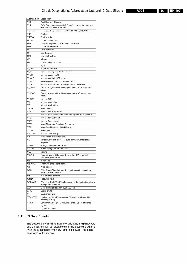
Circuit Descriptions, Abbreviation List, and IC Data Sheets EN 107A02E 9.
9.11 IC Data Sheets
This section shows the internal block diagrams and pin layouts of ICs that are drawn as "black boxes" in the electrical diagrams (with the exception of "memory" and "logic" ICs). This is not applicable to this manual.
THD Total Harmonic Distortion
TILT PWM Output signal (variable DC level) to control the picture tilt from the DOP block of the ADOC.
Trinorma Video standard, combination of PAL N, PAL M, NTSC M
TXT Teletext
TXTSW Teletext switch
U_100 U from Feature Box
UART Universal Asynchronous Receiver Transmitter
UBE Ultra Bass Enhancement
uC Micro controller
UI User Interface
UOC Ultimate One Chip
uP Microprocessor
UV Colour difference signals
V V_sync
V_100 V from Feature Box
V_2FH Vertical sync input for the 2fH source.
V_A50 Vertical Acquisition 1fH
V_AMP Vertical Amplitude DAC output
V_BAT Main supply for deflection (usually 141 V)
V_D100 Vertical Drive 2fH: vertical sync pulse from deflection
V_DNEG One of the symmetrical drive signals for the DC frame output stage.
V_DPOS One of the symmetrical drive signals for the DC frame output stage.
V_OSD Vertical OSD
VA Vertical Acquisition
VBI Vertical Blank Interval
V-chip Violence chip
VCR Video Cassette Recorder
VD Vertical Drive: vertical sync pulse coming from the feature box
VDS Virtual Dolby Surround
VERT Vertical Output pulse
VESA Video Electronics Standards Association
VGA Video Graphics Array: 640x480 (4:3)
VGND Video ground
VGUARD Vertical guard voltage
VIF Video Intermediate Frequency
VL Variable Level out: processed audio output toward external amplifier
VMEM Voltage supplied for EEPROM
VMICRO Power supply for micro controller
VOL Volume
VSYNC Pulse derived of 530 s-circuit behind the HOP, to vertically synchronize the Painter
WD Watch Dog
WE-NVM NVM write enable control line.
WS Wide Screen
WSS Wide Screen Signaling, used by broadcasters to transmit e.g. PALPLUS and Aspect Ratio
WST World System Teletext
WXGA 1280x768 (15:9)
WYSIWYR What You See Is What You Record: record selection that follows main picture and sound
XGA Extended Graphics Array: 1024x768 (4:3)
XTAL Quartz crystal
Y Luminance signal
YC (or Y/C) Luminance (Y) and Chrominance (C) signal (analogue video encoding format)
YPbPr Component video (Y= Luminance, Pb/ Pr= Colour difference signals)
YUV Component video
Abbreviation Description
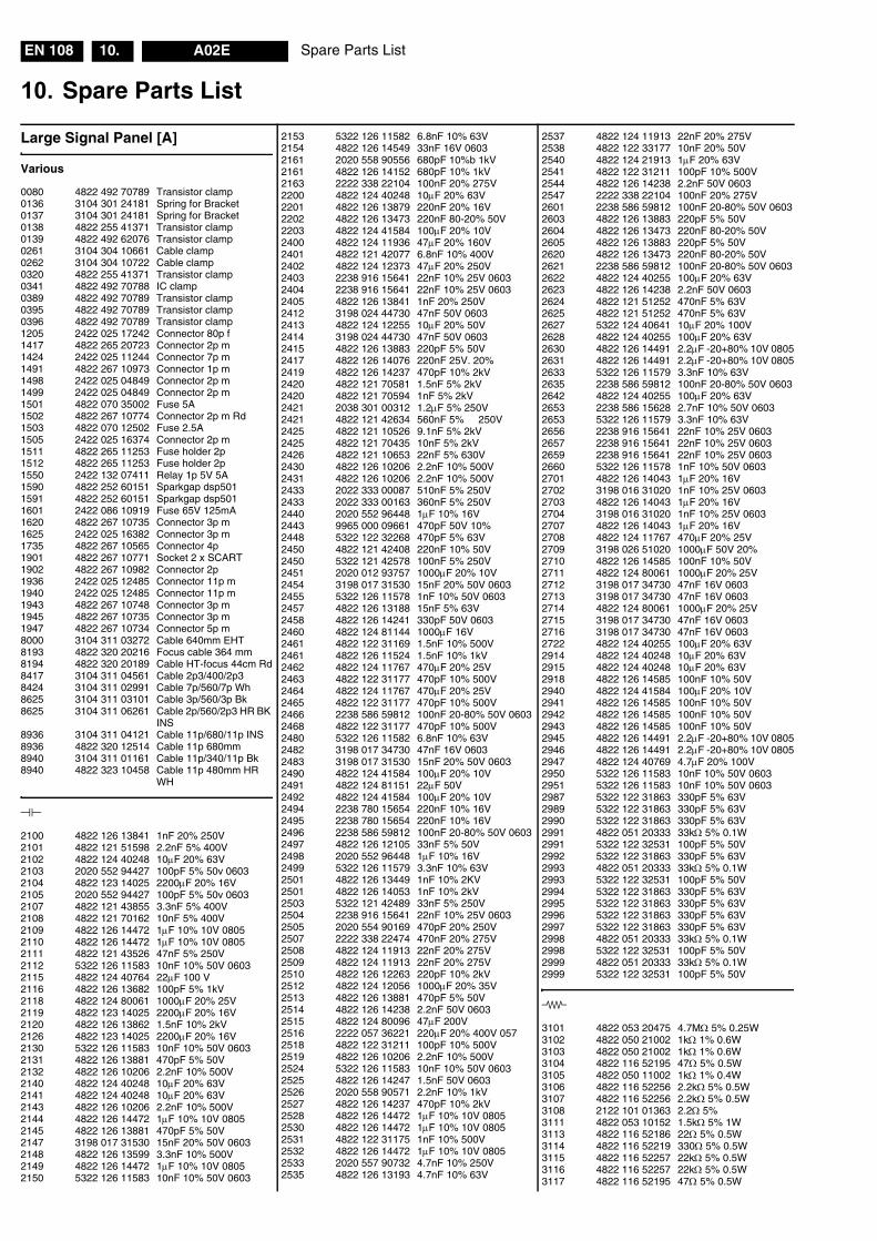
Spare Parts ListEN 108 A02E10.
10. Spare Parts List
Large Signal Panel [A]
Various
0080 4822 492 70789 Transistor clamp0136 3104 301 24181 Spring for Bracket0137 3104 301 24181 Spring for Bracket0138 4822 255 41371 Transistor clamp0139 4822 492 62076 Transistor clamp0261 3104 304 10661 Cable clamp0262 3104 304 10722 Cable clamp0320 4822 255 41371 Transistor clamp0341 4822 492 70788 IC clamp0389 4822 492 70789 Transistor clamp0395 4822 492 70789 Transistor clamp0396 4822 492 70789 Transistor clamp1205 2422 025 17242 Connector 80p f1417 4822 265 20723 Connector 2p m1424 2422 025 11244 Connector 7p m1491 4822 267 10973 Connector 1p m1498 2422 025 04849 Connector 2p m1499 2422 025 04849 Connector 2p m1501 4822 070 35002 Fuse 5A1502 4822 267 10774 Connector 2p m Rd1503 4822 070 12502 Fuse 2.5A1505 2422 025 16374 Connector 2p m1511 4822 265 11253 Fuse holder 2p1512 4822 265 11253 Fuse holder 2p1550 2422 132 07411 Relay 1p 5V 5A1590 4822 252 60151 Sparkgap dsp5011591 4822 252 60151 Sparkgap dsp5011601 2422 086 10919 Fuse 65V 125mA1620 4822 267 10735 Connector 3p m1625 2422 025 16382 Connector 3p m1735 4822 267 10565 Connector 4p1901 4822 267 10771 Socket 2 x SCART1902 4822 267 10982 Connector 2p1936 2422 025 12485 Connector 11p m1940 2422 025 12485 Connector 11p m1943 4822 267 10748 Connector 3p m1945 4822 267 10735 Connector 3p m1947 4822 267 10734 Connector 5p m8000 3104 311 03272 Cable 640mm EHT8193 4822 320 20216 Focus cable 364 mm8194 4822 320 20189 Cable HT-focus 44cm Rd8417 3104 311 04561 Cable 2p3/400/2p38424 3104 311 02991 Cable 7p/560/7p Wh8625 3104 311 03101 Cable 3p/560/3p Bk8625 3104 311 06261 Cable 2p/560/2p3 HR BK
INS8936 3104 311 04121 Cable 11p/680/11p INS8936 4822 320 12514 Cable 11p 680mm8940 3104 311 01161 Cable 11p/340/11p Bk8940 4822 323 10458 Cable 11p 480mm HR
WH
2100 4822 126 13841 1nF 20% 250V2101 4822 121 51598 2.2nF 5% 400V2102 4822 124 40248 10µF 20% 63V2103 2020 552 94427 100pF 5% 50v 06032104 4822 123 14025 2200µF 20% 16V2105 2020 552 94427 100pF 5% 50v 06032107 4822 121 43855 3.3nF 5% 400V2108 4822 121 70162 10nF 5% 400V2109 4822 126 14472 1µF 10% 10V 08052110 4822 126 14472 1µF 10% 10V 08052111 4822 121 43526 47nF 5% 250V2112 5322 126 11583 10nF 10% 50V 06032115 4822 124 40764 22µF 100 V2116 4822 126 13682 100pF 5% 1kV2118 4822 124 80061 1000µF 20% 25V2119 4822 123 14025 2200µF 20% 16V2120 4822 126 13862 1.5nF 10% 2kV2126 4822 123 14025 2200µF 20% 16V2130 5322 126 11583 10nF 10% 50V 06032131 4822 126 13881 470pF 5% 50V2132 4822 126 10206 2.2nF 10% 500V2140 4822 124 40248 10µF 20% 63V2141 4822 124 40248 10µF 20% 63V2143 4822 126 10206 2.2nF 10% 500V2144 4822 126 14472 1µF 10% 10V 08052145 4822 126 13881 470pF 5% 50V2147 3198 017 31530 15nF 20% 50V 06032148 4822 126 13599 3.3nF 10% 500V2149 4822 126 14472 1µF 10% 10V 08052150 5322 126 11583 10nF 10% 50V 0603
2153 5322 126 11582 6.8nF 10% 63V2154 4822 126 14549 33nF 16V 06032161 2020 558 90556 680pF 10%b 1kV2161 4822 126 14152 680pF 10% 1kV2163 2222 338 22104 100nF 20% 275V2200 4822 124 40248 10µF 20% 63V2201 4822 126 13879 220nF 20% 16V2202 4822 126 13473 220nF 80-20% 50V2203 4822 124 41584 100µF 20% 10V2400 4822 124 11936 47µF 20% 160V2401 4822 121 42077 6.8nF 10% 400V2402 4822 124 12373 47µF 20% 250V2403 2238 916 15641 22nF 10% 25V 06032404 2238 916 15641 22nF 10% 25V 06032405 4822 126 13841 1nF 20% 250V2412 3198 024 44730 47nF 50V 06032413 4822 124 12255 10µF 20% 50V2414 3198 024 44730 47nF 50V 06032415 4822 126 13883 220pF 5% 50V2417 4822 126 14076 220nF 25V. 20%2419 4822 126 14237 470pF 10% 2kV2420 4822 121 70581 1.5nF 5% 2kV2420 4822 121 70594 1nF 5% 2kV2421 2038 301 00312 1.2µF 5% 250V2421 4822 121 42634 560nF 5% 250V2425 4822 121 10526 9.1nF 5% 2kV2425 4822 121 70435 10nF 5% 2kV2426 4822 121 10653 22nF 5% 630V2430 4822 126 10206 2.2nF 10% 500V2431 4822 126 10206 2.2nF 10% 500V2433 2022 333 00087 510nF 5% 250V2433 2022 333 00163 360nF 5% 250V2440 2020 552 96448 1µF 10% 16V2443 9965 000 09661 470pF 50V 10%2448 5322 122 32268 470pF 5% 63V2450 4822 121 42408 220nF 10% 50V2450 5322 121 42578 100nF 5% 250V2451 2020 012 93757 1000µF 20% 10V2454 3198 017 31530 15nF 20% 50V 06032455 5322 126 11578 1nF 10% 50V 06032457 4822 126 13188 15nF 5% 63V2458 4822 126 14241 330pF 50V 06032460 4822 124 81144 1000µF 16V2461 4822 122 31169 1.5nF 10% 500V2461 4822 126 11524 1.5nF 10% 1kV2462 4822 124 11767 470µF 20% 25V2463 4822 122 31177 470pF 10% 500V2464 4822 124 11767 470µF 20% 25V2465 4822 122 31177 470pF 10% 500V2466 2238 586 59812 100nF 20-80% 50V 06032468 4822 122 31177 470pF 10% 500V2480 5322 126 11582 6.8nF 10% 63V2482 3198 017 34730 47nF 16V 06032483 3198 017 31530 15nF 20% 50V 06032490 4822 124 41584 100µF 20% 10V2491 4822 124 81151 22µF 50V2492 4822 124 41584 100µF 20% 10V2494 2238 780 15654 220nF 10% 16V2495 2238 780 15654 220nF 10% 16V2496 2238 586 59812 100nF 20-80% 50V 06032497 4822 126 12105 33nF 5% 50V2498 2020 552 96448 1µF 10% 16V2499 5322 126 11579 3.3nF 10% 63V2501 4822 126 13449 1nF 10% 2KV2501 4822 126 14053 1nF 10% 2kV2503 5322 121 42489 33nF 5% 250V2504 2238 916 15641 22nF 10% 25V 06032505 2020 554 90169 470pF 20% 250V2507 2222 338 22474 470nF 20% 275V2508 4822 124 11913 22nF 20% 275V2509 4822 124 11913 22nF 20% 275V2510 4822 126 12263 220pF 10% 2kV2512 4822 124 12056 1000µF 20% 35V2513 4822 126 13881 470pF 5% 50V2514 4822 126 14238 2.2nF 50V 06032515 4822 124 80096 47µF 200V2516 2222 057 36221 220µF 20% 400V 0572518 4822 122 31211 100pF 10% 500V2519 4822 126 10206 2.2nF 10% 500V2524 5322 126 11583 10nF 10% 50V 06032525 4822 126 14247 1.5nF 50V 06032526 2020 558 90571 2.2nF 10% 1kV2527 4822 126 14237 470pF 10% 2kV2528 4822 126 14472 1µF 10% 10V 08052530 4822 126 14472 1µF 10% 10V 08052531 4822 122 31175 1nF 10% 500V2532 4822 126 14472 1µF 10% 10V 08052533 2020 557 90732 4.7nF 10% 250V2535 4822 126 13193 4.7nF 10% 63V
2537 4822 124 11913 22nF 20% 275V2538 4822 122 33177 10nF 20% 50V2540 4822 124 21913 1µF 20% 63V2541 4822 122 31211 100pF 10% 500V2544 4822 126 14238 2.2nF 50V 06032547 2222 338 22104 100nF 20% 275V2601 2238 586 59812 100nF 20-80% 50V 06032603 4822 126 13883 220pF 5% 50V2604 4822 126 13473 220nF 80-20% 50V2605 4822 126 13883 220pF 5% 50V2620 4822 126 13473 220nF 80-20% 50V2621 2238 586 59812 100nF 20-80% 50V 06032622 4822 124 40255 100µF 20% 63V2623 4822 126 14238 2.2nF 50V 06032624 4822 121 51252 470nF 5% 63V2625 4822 121 51252 470nF 5% 63V2627 5322 124 40641 10µF 20% 100V2628 4822 124 40255 100µF 20% 63V2630 4822 126 14491 2.2µF -20+80% 10V 08052631 4822 126 14491 2.2µF -20+80% 10V 08052633 5322 126 11579 3.3nF 10% 63V2635 2238 586 59812 100nF 20-80% 50V 06032642 4822 124 40255 100µF 20% 63V2653 2238 586 15628 2.7nF 10% 50V 06032653 5322 126 11579 3.3nF 10% 63V2656 2238 916 15641 22nF 10% 25V 06032657 2238 916 15641 22nF 10% 25V 06032659 2238 916 15641 22nF 10% 25V 06032660 5322 126 11578 1nF 10% 50V 06032701 4822 126 14043 1µF 20% 16V2702 3198 016 31020 1nF 10% 25V 06032703 4822 126 14043 1µF 20% 16V2704 3198 016 31020 1nF 10% 25V 06032707 4822 126 14043 1µF 20% 16V2708 4822 124 11767 470µF 20% 25V2709 3198 026 51020 1000µF 50V 20%2710 4822 126 14585 100nF 10% 50V2711 4822 124 80061 1000µF 20% 25V2712 3198 017 34730 47nF 16V 06032713 3198 017 34730 47nF 16V 06032714 4822 124 80061 1000µF 20% 25V2715 3198 017 34730 47nF 16V 06032716 3198 017 34730 47nF 16V 06032722 4822 124 40255 100µF 20% 63V2914 4822 124 40248 10µF 20% 63V2915 4822 124 40248 10µF 20% 63V2918 4822 126 14585 100nF 10% 50V2940 4822 124 41584 100µF 20% 10V2941 4822 126 14585 100nF 10% 50V2942 4822 126 14585 100nF 10% 50V2943 4822 126 14585 100nF 10% 50V2945 4822 126 14491 2.2µF -20+80% 10V 08052946 4822 126 14491 2.2µF -20+80% 10V 08052947 4822 124 40769 4.7µF 20% 100V2950 5322 126 11583 10nF 10% 50V 06032951 5322 126 11583 10nF 10% 50V 06032987 5322 122 31863 330pF 5% 63V2989 5322 122 31863 330pF 5% 63V2990 5322 122 31863 330pF 5% 63V2991 4822 051 20333 33kΩ 5% 0.1W2991 5322 122 32531 100pF 5% 50V2992 5322 122 31863 330pF 5% 63V2993 4822 051 20333 33kΩ 5% 0.1W2993 5322 122 32531 100pF 5% 50V2994 5322 122 31863 330pF 5% 63V2995 5322 122 31863 330pF 5% 63V2996 5322 122 31863 330pF 5% 63V2997 5322 122 31863 330pF 5% 63V2998 4822 051 20333 33kΩ 5% 0.1W2998 5322 122 32531 100pF 5% 50V2999 4822 051 20333 33kΩ 5% 0.1W2999 5322 122 32531 100pF 5% 50V
3101 4822 053 20475 4.7MΩ 5% 0.25W3102 4822 050 21002 1kΩ 1% 0.6W3103 4822 050 21002 1kΩ 1% 0.6W3104 4822 116 52195 47Ω 5% 0.5W3105 4822 050 11002 1kΩ 1% 0.4W3106 4822 116 52256 2.2kΩ 5% 0.5W3107 4822 116 52256 2.2kΩ 5% 0.5W3108 2122 101 01363 2.2Ω 5%3111 4822 053 10152 1.5kΩ 5% 1W3113 4822 116 52186 22Ω 5% 0.5W3114 4822 116 52219 330Ω 5% 0.5W3115 4822 116 52257 22kΩ 5% 0.5W3116 4822 116 52257 22kΩ 5% 0.5W3117 4822 116 52195 47Ω 5% 0.5W
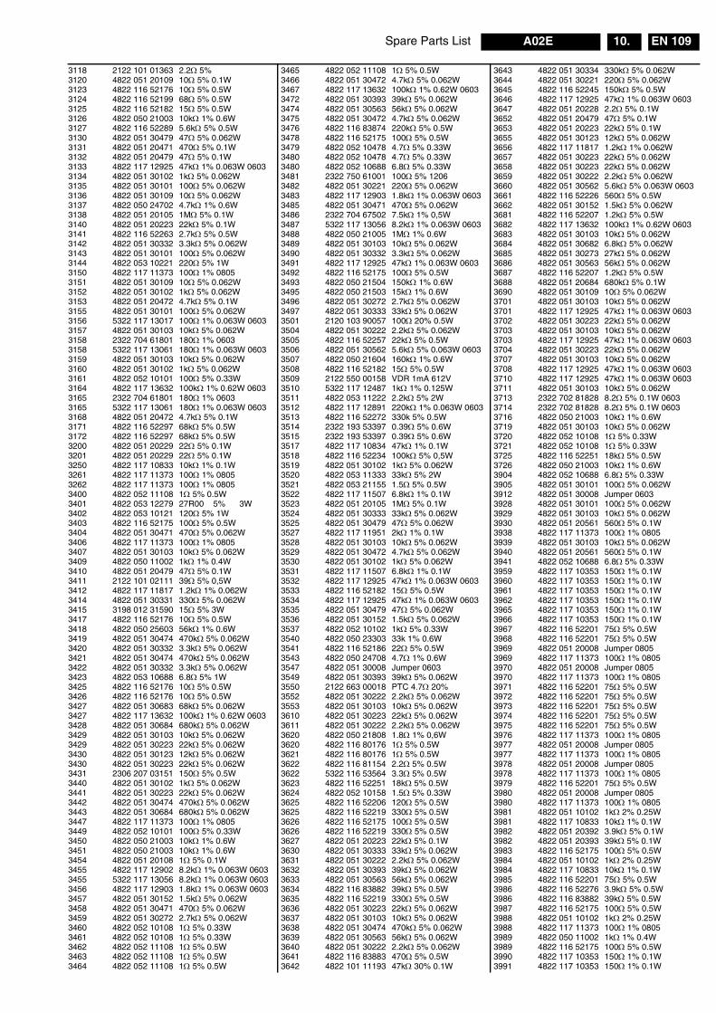
Spare Parts List EN 109A02E 10.
3118 2122 101 01363 2.2Ω 5%3120 4822 051 20109 10Ω 5% 0.1W3123 4822 116 52176 10Ω 5% 0.5W3124 4822 116 52199 68Ω 5% 0.5W3125 4822 116 52182 15Ω 5% 0.5W3126 4822 050 21003 10kΩ 1% 0.6W3127 4822 116 52289 5.6kΩ 5% 0.5W3130 4822 051 30479 47Ω 5% 0.062W3131 4822 051 20471 470Ω 5% 0.1W3132 4822 051 20479 47Ω 5% 0.1W3133 4822 117 12925 47kΩ 1% 0.063W 06033134 4822 051 30102 1kΩ 5% 0.062W3135 4822 051 30101 100Ω 5% 0.062W3136 4822 051 30109 10Ω 5% 0.062W3137 4822 050 24702 4.7kΩ 1% 0.6W3138 4822 051 20105 1MΩ 5% 0.1W3140 4822 051 20223 22kΩ 5% 0.1W3141 4822 116 52263 2.7kΩ 5% 0.5W3142 4822 051 30332 3.3kΩ 5% 0.062W3143 4822 051 30101 100Ω 5% 0.062W3144 4822 053 10221 220Ω 5% 1W3150 4822 117 11373 100Ω 1% 08053151 4822 051 30109 10Ω 5% 0.062W3152 4822 051 30102 1kΩ 5% 0.062W3153 4822 051 20472 4.7kΩ 5% 0.1W3155 4822 051 30101 100Ω 5% 0.062W3156 5322 117 13017 100Ω 1% 0.063W 06033157 4822 051 30103 10kΩ 5% 0.062W3158 2322 704 61801 180Ω 1% 06033158 5322 117 13061 180Ω 1% 0.063W 06033159 4822 051 30103 10kΩ 5% 0.062W3160 4822 051 30102 1kΩ 5% 0.062W3161 4822 052 10101 100Ω 5% 0.33W3164 4822 117 13632 100kΩ 1% 0.62W 06033165 2322 704 61801 180Ω 1% 06033165 5322 117 13061 180Ω 1% 0.063W 06033168 4822 051 20472 4.7kΩ 5% 0.1W3171 4822 116 52297 68kΩ 5% 0.5W3172 4822 116 52297 68kΩ 5% 0.5W3200 4822 051 20229 22Ω 5% 0.1W3201 4822 051 20229 22Ω 5% 0.1W3250 4822 117 10833 10kΩ 1% 0.1W3261 4822 117 11373 100Ω 1% 08053262 4822 117 11373 100Ω 1% 08053400 4822 052 11108 1Ω 5% 0.5W3401 4822 053 12279 27R00 5% 3W3402 4822 053 10121 120Ω 5% 1W3403 4822 116 52175 100Ω 5% 0.5W3404 4822 051 30471 470Ω 5% 0.062W3406 4822 117 11373 100Ω 1% 08053407 4822 051 30103 10kΩ 5% 0.062W3409 4822 050 11002 1kΩ 1% 0.4W3410 4822 051 20479 47Ω 5% 0.1W3411 2122 101 02111 39Ω 5% 0,5W3412 4822 117 11817 1.2kΩ 1% 0.062W3414 4822 051 30331 330Ω 5% 0.062W3415 3198 012 31590 15Ω 5% 3W3417 4822 116 52176 10Ω 5% 0.5W3418 4822 050 25603 56kΩ 1% 0.6W3419 4822 051 30474 470kΩ 5% 0.062W3420 4822 051 30332 3.3kΩ 5% 0.062W3421 4822 051 30474 470kΩ 5% 0.062W3422 4822 051 30332 3.3kΩ 5% 0.062W3423 4822 053 10688 6.8Ω 5% 1W3425 4822 116 52176 10Ω 5% 0.5W3426 4822 116 52176 10Ω 5% 0.5W3427 4822 051 30683 68kΩ 5% 0.062W3427 4822 117 13632 100kΩ 1% 0.62W 06033428 4822 051 30684 680kΩ 5% 0.062W3429 4822 051 30103 10kΩ 5% 0.062W3429 4822 051 30223 22kΩ 5% 0.062W3430 4822 051 30123 12kΩ 5% 0.062W3430 4822 051 30223 22kΩ 5% 0.062W3431 2306 207 03151 150Ω 5% 0.5W3440 4822 051 30102 1kΩ 5% 0.062W3441 4822 051 30223 22kΩ 5% 0.062W3442 4822 051 30474 470kΩ 5% 0.062W3443 4822 051 30684 680kΩ 5% 0.062W3447 4822 117 11373 100Ω 1% 08053449 4822 052 10101 100Ω 5% 0.33W3450 4822 050 21003 10kΩ 1% 0.6W3451 4822 050 21003 10kΩ 1% 0.6W3454 4822 051 20108 1Ω 5% 0.1W3455 4822 117 12902 8.2kΩ 1% 0.063W 06033455 5322 117 13056 8.2kΩ 1% 0.063W 06033456 4822 117 12903 1.8kΩ 1% 0.063W 06033457 4822 051 30152 1.5kΩ 5% 0.062W3458 4822 051 30471 470Ω 5% 0.062W3459 4822 051 30272 2.7kΩ 5% 0.062W3460 4822 052 10108 1Ω 5% 0.33W3461 4822 052 10108 1Ω 5% 0.33W3462 4822 052 11108 1Ω 5% 0.5W3463 4822 052 11108 1Ω 5% 0.5W3464 4822 052 11108 1Ω 5% 0.5W
3465 4822 052 11108 1Ω 5% 0.5W3466 4822 051 30472 4.7kΩ 5% 0.062W3467 4822 117 13632 100kΩ 1% 0.62W 06033472 4822 051 30393 39kΩ 5% 0.062W3474 4822 051 30563 56kΩ 5% 0.062W3475 4822 051 30472 4.7kΩ 5% 0.062W3476 4822 116 83874 220kΩ 5% 0.5W3478 4822 116 52175 100Ω 5% 0.5W3479 4822 052 10478 4.7Ω 5% 0.33W3480 4822 052 10478 4.7Ω 5% 0.33W3480 4822 052 10688 6.8Ω 5% 0.33W3481 2322 750 61001 100Ω 5% 12063482 4822 051 30221 220Ω 5% 0.062W3483 4822 117 12903 1.8kΩ 1% 0.063W 06033485 4822 051 30471 470Ω 5% 0.062W3486 2322 704 67502 7.5kΩ 1% 0,5W3487 5322 117 13056 8.2kΩ 1% 0.063W 06033488 4822 050 21005 1MΩ 1% 0.6W3489 4822 051 30103 10kΩ 5% 0.062W3490 4822 051 30332 3.3kΩ 5% 0.062W3491 4822 117 12925 47kΩ 1% 0.063W 06033492 4822 116 52175 100Ω 5% 0.5W3493 4822 050 21504 150kΩ 1% 0.6W3495 4822 050 21503 15kΩ 1% 0.6W3496 4822 051 30272 2.7kΩ 5% 0.062W3497 4822 051 30333 33kΩ 5% 0.062W3501 2120 103 90057 100Ω 20% 0.5W3504 4822 051 30222 2.2kΩ 5% 0.062W3505 4822 116 52257 22kΩ 5% 0.5W3506 4822 051 30562 5.6kΩ 5% 0.063W 06033507 4822 050 21604 160kΩ 1% 0.6W3508 4822 116 52182 15Ω 5% 0.5W3509 2122 550 00158 VDR 1mA 612V3510 5322 117 12487 1kΩ 1% 0.125W3511 4822 053 11222 2.2kΩ 5% 2W3512 4822 117 12891 220kΩ 1% 0.063W 06033513 4822 116 52272 330k 5% 0.5W3514 2322 193 53397 0.39Ω 5% 0.6W3515 2322 193 53397 0.39Ω 5% 0.6W3517 4822 117 10834 47kΩ 1% 0.1W3518 4822 116 52234 100kΩ 5% 0,5W3519 4822 051 30102 1kΩ 5% 0.062W3520 4822 053 11333 33kΩ 5% 2W3521 4822 053 21155 1.5Ω 5% 0.5W3522 4822 117 11507 6.8kΩ 1% 0.1W3523 4822 051 20105 1MΩ 5% 0.1W3524 4822 051 30333 33kΩ 5% 0.062W3525 4822 051 30479 47Ω 5% 0.062W3527 4822 117 11951 2kΩ 1% 0.1W3528 4822 051 30103 10kΩ 5% 0.062W3529 4822 051 30472 4.7kΩ 5% 0.062W3530 4822 051 30102 1kΩ 5% 0.062W3531 4822 117 11507 6.8kΩ 1% 0.1W3532 4822 117 12925 47kΩ 1% 0.063W 06033533 4822 116 52182 15Ω 5% 0.5W3534 4822 117 12925 47kΩ 1% 0.063W 06033535 4822 051 30479 47Ω 5% 0.062W3536 4822 051 30152 1.5kΩ 5% 0.062W3537 4822 052 10102 1kΩ 5% 0.33W3540 4822 050 23303 33k 1% 0.6W3541 4822 116 52186 22Ω 5% 0.5W3543 4822 050 24708 4.7Ω 1% 0.6W3547 4822 051 30008 Jumper 06033549 4822 051 30393 39kΩ 5% 0.062W3550 2122 663 00018 PTC 4.7Ω 20%3552 4822 051 30222 2.2kΩ 5% 0.062W3553 4822 051 30103 10kΩ 5% 0.062W3610 4822 051 30223 22kΩ 5% 0.062W3611 4822 051 30222 2.2kΩ 5% 0.062W3620 4822 050 21808 1.8Ω 1% 0,6W3620 4822 116 80176 1Ω 5% 0.5W3621 4822 116 80176 1Ω 5% 0.5W3622 4822 116 81154 2.2Ω 5% 0.5W3622 5322 116 53564 3.3Ω 5% 0.5W3623 4822 116 52251 18kΩ 5% 0.5W3624 4822 052 10158 1.5Ω 5% 0.33W3625 4822 116 52206 120Ω 5% 0.5W3625 4822 116 52219 330Ω 5% 0.5W3626 4822 116 52175 100Ω 5% 0.5W3626 4822 116 52219 330Ω 5% 0.5W3627 4822 051 20223 22kΩ 5% 0.1W3630 4822 051 30333 33kΩ 5% 0.062W3631 4822 051 30222 2.2kΩ 5% 0.062W3632 4822 051 30393 39kΩ 5% 0.062W3633 4822 051 30563 56kΩ 5% 0.062W3634 4822 116 83882 39kΩ 5% 0.5W3635 4822 116 52219 330Ω 5% 0.5W3636 4822 051 30223 22kΩ 5% 0.062W3637 4822 051 30103 10kΩ 5% 0.062W3638 4822 051 30474 470kΩ 5% 0.062W3639 4822 051 30563 56kΩ 5% 0.062W3640 4822 051 30222 2.2kΩ 5% 0.062W3641 4822 116 83883 470Ω 5% 0.5W3642 4822 101 11193 47kΩ 30% 0.1W
3643 4822 051 30334 330kΩ 5% 0.062W3644 4822 051 30221 220Ω 5% 0.062W3645 4822 116 52245 150kΩ 5% 0.5W3646 4822 117 12925 47kΩ 1% 0.063W 06033647 4822 051 20228 2.2Ω 5% 0.1W3652 4822 051 20479 47Ω 5% 0.1W3653 4822 051 20223 22kΩ 5% 0.1W3655 4822 051 30123 12kΩ 5% 0.062W3656 4822 117 11817 1.2kΩ 1% 0.062W3657 4822 051 30223 22kΩ 5% 0.062W3658 4822 051 30223 22kΩ 5% 0.062W3659 4822 051 30222 2.2kΩ 5% 0.062W3660 4822 051 30562 5.6kΩ 5% 0.063W 06033661 4822 116 52226 560Ω 5% 0.5W3662 4822 051 30152 1.5kΩ 5% 0.062W3681 4822 116 52207 1.2kΩ 5% 0.5W3682 4822 117 13632 100kΩ 1% 0.62W 06033683 4822 051 30103 10kΩ 5% 0.062W3684 4822 051 30682 6.8kΩ 5% 0.062W3685 4822 051 30273 27kΩ 5% 0.062W3686 4822 051 30563 56kΩ 5% 0.062W3687 4822 116 52207 1.2kΩ 5% 0.5W3688 4822 051 20684 680kΩ 5% 0.1W3690 4822 051 30109 10Ω 5% 0.062W3701 4822 051 30103 10kΩ 5% 0.062W3701 4822 117 12925 47kΩ 1% 0.063W 06033702 4822 051 30223 22kΩ 5% 0.062W3703 4822 051 30103 10kΩ 5% 0.062W3703 4822 117 12925 47kΩ 1% 0.063W 06033704 4822 051 30223 22kΩ 5% 0.062W3707 4822 051 30103 10kΩ 5% 0.062W3708 4822 117 12925 47kΩ 1% 0.063W 06033710 4822 117 12925 47kΩ 1% 0.063W 06033711 4822 051 30103 10kΩ 5% 0.062W3713 2322 702 81828 8.2Ω 5% 0.1W 06033714 2322 702 81828 8.2Ω 5% 0.1W 06033716 4822 050 21003 10kΩ 1% 0.6W3719 4822 051 30103 10kΩ 5% 0.062W3720 4822 052 10108 1Ω 5% 0.33W3721 4822 052 10108 1Ω 5% 0.33W3725 4822 116 52251 18kΩ 5% 0.5W3726 4822 050 21003 10kΩ 1% 0.6W3904 4822 052 10688 6.8Ω 5% 0.33W3905 4822 051 30101 100Ω 5% 0.062W3912 4822 051 30008 Jumper 06033928 4822 051 30101 100Ω 5% 0.062W3929 4822 051 30103 10kΩ 5% 0.062W3930 4822 051 20561 560Ω 5% 0.1W3938 4822 117 11373 100Ω 1% 08053939 4822 051 30103 10kΩ 5% 0.062W3940 4822 051 20561 560Ω 5% 0.1W3941 4822 052 10688 6.8Ω 5% 0.33W3959 4822 117 10353 150Ω 1% 0.1W3960 4822 117 10353 150Ω 1% 0.1W3961 4822 117 10353 150Ω 1% 0.1W3962 4822 117 10353 150Ω 1% 0.1W3965 4822 117 10353 150Ω 1% 0.1W3966 4822 117 10353 150Ω 1% 0.1W3967 4822 116 52201 75Ω 5% 0.5W3968 4822 116 52201 75Ω 5% 0.5W3969 4822 051 20008 Jumper 08053969 4822 117 11373 100Ω 1% 08053970 4822 051 20008 Jumper 08053970 4822 117 11373 100Ω 1% 08053971 4822 116 52201 75Ω 5% 0.5W3972 4822 116 52201 75Ω 5% 0.5W3973 4822 116 52201 75Ω 5% 0.5W3974 4822 116 52201 75Ω 5% 0.5W3975 4822 116 52201 75Ω 5% 0.5W3976 4822 117 11373 100Ω 1% 08053977 4822 051 20008 Jumper 08053977 4822 117 11373 100Ω 1% 08053978 4822 051 20008 Jumper 08053978 4822 117 11373 100Ω 1% 08053979 4822 116 52201 75Ω 5% 0.5W3980 4822 051 20008 Jumper 08053980 4822 117 11373 100Ω 1% 08053981 4822 051 10102 1kΩ 2% 0.25W3981 4822 117 10833 10kΩ 1% 0.1W3982 4822 051 20392 3.9kΩ 5% 0.1W3982 4822 051 20393 39kΩ 5% 0.1W3983 4822 116 52175 100Ω 5% 0.5W3984 4822 051 10102 1kΩ 2% 0.25W3984 4822 117 10833 10kΩ 1% 0.1W3985 4822 116 52201 75Ω 5% 0.5W3986 4822 116 52276 3.9kΩ 5% 0.5W3986 4822 116 83882 39kΩ 5% 0.5W3987 4822 116 52175 100Ω 5% 0.5W3988 4822 051 10102 1kΩ 2% 0.25W3988 4822 117 11373 100Ω 1% 08053989 4822 050 11002 1kΩ 1% 0.4W3989 4822 116 52175 100Ω 5% 0.5W3990 4822 117 10353 150Ω 1% 0.1W3991 4822 117 10353 150Ω 1% 0.1W
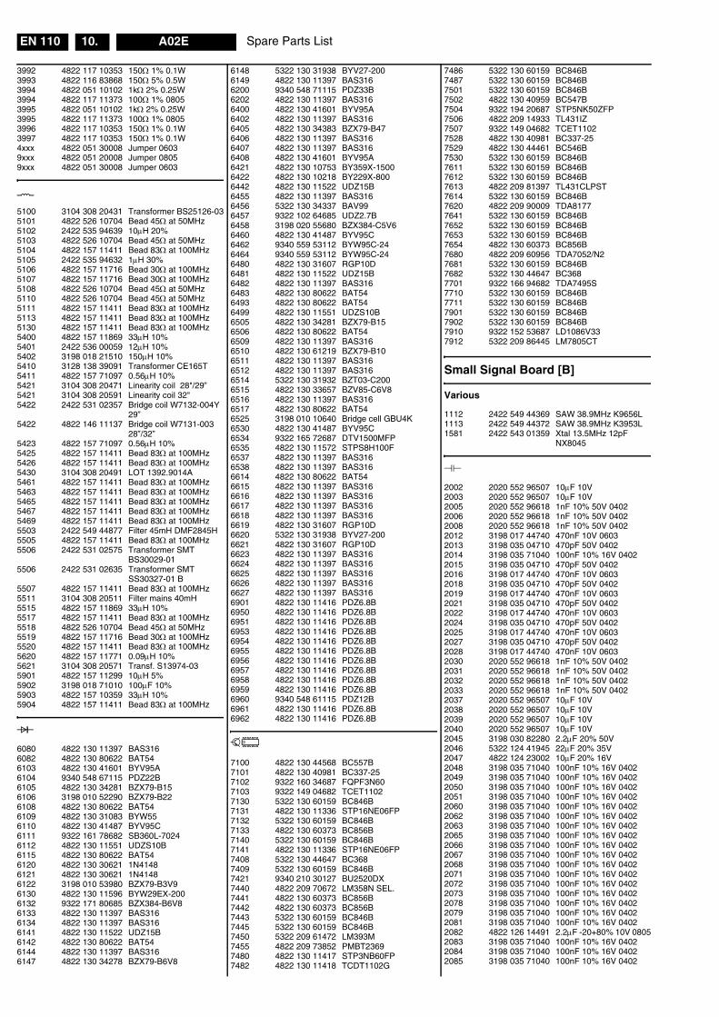
Spare Parts ListEN 110 A02E10.
3992 4822 117 10353 150Ω 1% 0.1W3993 4822 116 83868 150Ω 5% 0.5W3994 4822 051 10102 1kΩ 2% 0.25W3994 4822 117 11373 100Ω 1% 08053995 4822 051 10102 1kΩ 2% 0.25W3995 4822 117 11373 100Ω 1% 08053996 4822 117 10353 150Ω 1% 0.1W3997 4822 117 10353 150Ω 1% 0.1W4xxx 4822 051 30008 Jumper 06039xxx 4822 051 20008 Jumper 08059xxx 4822 051 30008 Jumper 0603
5100 3104 308 20431 Transformer BS25126-035101 4822 526 10704 Bead 45Ω at 50MHz5102 2422 535 94639 10µH 20%5103 4822 526 10704 Bead 45Ω at 50MHz5104 4822 157 11411 Bead 83Ω at 100MHz5105 2422 535 94632 1µH 30%5106 4822 157 11716 Bead 30Ω at 100MHz5107 4822 157 11716 Bead 30Ω at 100MHz5108 4822 526 10704 Bead 45Ω at 50MHz5110 4822 526 10704 Bead 45Ω at 50MHz5111 4822 157 11411 Bead 83Ω at 100MHz5113 4822 157 11411 Bead 83Ω at 100MHz5130 4822 157 11411 Bead 83Ω at 100MHz5400 4822 157 11869 33µH 10%5401 2422 536 00059 12µH 10%5402 3198 018 21510 150µH 10%5410 3128 138 39091 Transformer CE165T5411 4822 157 71097 0.56µH 10%5421 3104 308 20471 Linearity coil 28"/29”5421 3104 308 20591 Linearity coil 32"5422 2422 531 02357 Bridge coil W7132-004Y
29”5422 4822 146 11137 Bridge coil W7131-003
28”/32”5423 4822 157 71097 0.56µH 10%5425 4822 157 11411 Bead 83Ω at 100MHz5426 4822 157 11411 Bead 83Ω at 100MHz5430 3104 308 20491 LOT 1392.9014A5461 4822 157 11411 Bead 83Ω at 100MHz5463 4822 157 11411 Bead 83Ω at 100MHz5465 4822 157 11411 Bead 83Ω at 100MHz5467 4822 157 11411 Bead 83Ω at 100MHz5469 4822 157 11411 Bead 83Ω at 100MHz5503 2422 549 44877 Filter 45mH DMF2845H5505 4822 157 11411 Bead 83Ω at 100MHz5506 2422 531 02575 Transformer SMT
BS30029-015506 2422 531 02635 Transformer SMT
SS30327-01 B5507 4822 157 11411 Bead 83Ω at 100MHz5511 3104 308 20511 Filter mains 40mH5515 4822 157 11869 33µH 10%5517 4822 157 11411 Bead 83Ω at 100MHz5518 4822 526 10704 Bead 45Ω at 50MHz5519 4822 157 11716 Bead 30Ω at 100MHz5520 4822 157 11411 Bead 83Ω at 100MHz5620 4822 157 11771 0.09µH 10%5621 3104 308 20571 Transf. S13974-035901 4822 157 11299 10µH 5%5902 3198 018 71010 100µF 10%5903 4822 157 10359 33µH 10%5904 4822 157 11411 Bead 83Ω at 100MHz
6080 4822 130 11397 BAS3166082 4822 130 80622 BAT546103 4822 130 41601 BYV95A6104 9340 548 67115 PDZ22B6105 4822 130 34281 BZX79-B156106 3198 010 52290 BZX79-B226108 4822 130 80622 BAT546109 4822 130 31083 BYW556110 4822 130 41487 BYV95C6111 9322 161 78682 SB360L-70246112 4822 130 11551 UDZS10B6115 4822 130 80622 BAT546120 4822 130 30621 1N41486121 4822 130 30621 1N41486122 3198 010 53980 BZX79-B3V96130 4822 130 11596 BYW29EX-2006132 9322 171 80685 BZX384-B6V86133 4822 130 11397 BAS3166134 4822 130 11397 BAS3166141 4822 130 11522 UDZ15B6142 4822 130 80622 BAT546144 4822 130 11397 BAS3166147 4822 130 34278 BZX79-B6V8
6148 5322 130 31938 BYV27-2006149 4822 130 11397 BAS3166200 9340 548 71115 PDZ33B6202 4822 130 11397 BAS3166400 4822 130 41601 BYV95A6402 4822 130 11397 BAS3166405 4822 130 34383 BZX79-B476406 4822 130 11397 BAS3166407 4822 130 11397 BAS3166408 4822 130 41601 BYV95A6421 4822 130 10753 BY359X-15006422 4822 130 10218 BY229X-8006442 4822 130 11522 UDZ15B6455 4822 130 11397 BAS3166456 5322 130 34337 BAV996457 9322 102 64685 UDZ2.7B6458 3198 020 55680 BZX384-C5V66460 4822 130 41487 BYV95C6462 9340 559 53112 BYW95C-246464 9340 559 53112 BYW95C-246480 4822 130 31607 RGP10D6481 4822 130 11522 UDZ15B6482 4822 130 11397 BAS3166483 4822 130 80622 BAT546493 4822 130 80622 BAT546499 4822 130 11551 UDZS10B6505 4822 130 34281 BZX79-B156506 4822 130 80622 BAT546509 4822 130 11397 BAS3166510 4822 130 61219 BZX79-B106511 4822 130 11397 BAS3166512 4822 130 11397 BAS3166514 5322 130 31932 BZT03-C2006515 4822 130 33657 BZV85-C6V86516 4822 130 11397 BAS3166517 4822 130 80622 BAT546525 3198 010 10640 Bridge cell GBU4K6530 4822 130 41487 BYV95C6534 9322 165 72687 DTV1500MFP6535 4822 130 11572 STPS8H100F6537 4822 130 11397 BAS3166538 4822 130 11397 BAS3166614 4822 130 80622 BAT546615 4822 130 11397 BAS3166616 4822 130 11397 BAS3166617 4822 130 11397 BAS3166618 4822 130 11397 BAS3166619 4822 130 31607 RGP10D6620 5322 130 31938 BYV27-2006621 4822 130 31607 RGP10D6623 4822 130 11397 BAS3166624 4822 130 11397 BAS3166625 4822 130 11397 BAS3166626 4822 130 11397 BAS3166627 4822 130 11397 BAS3166901 4822 130 11416 PDZ6.8B6950 4822 130 11416 PDZ6.8B6951 4822 130 11416 PDZ6.8B6953 4822 130 11416 PDZ6.8B6954 4822 130 11416 PDZ6.8B6955 4822 130 11416 PDZ6.8B6956 4822 130 11416 PDZ6.8B6957 4822 130 11416 PDZ6.8B6958 4822 130 11416 PDZ6.8B6959 4822 130 11416 PDZ6.8B6960 9340 548 61115 PDZ12B6961 4822 130 11416 PDZ6.8B6962 4822 130 11416 PDZ6.8B
7100 4822 130 44568 BC557B7101 4822 130 40981 BC337-257102 9322 160 34687 FQPF3N607103 9322 149 04682 TCET11027130 5322 130 60159 BC846B7131 4822 130 11336 STP16NE06FP7132 5322 130 60159 BC846B7133 4822 130 60373 BC856B7140 5322 130 60159 BC846B7141 4822 130 11336 STP16NE06FP7408 5322 130 44647 BC3687409 5322 130 60159 BC846B7421 9340 210 30127 BU2520DX7440 4822 209 70672 LM358N SEL.7441 4822 130 60373 BC856B7442 4822 130 60373 BC856B7443 5322 130 60159 BC846B7445 5322 130 60159 BC846B7450 5322 209 61472 LM393M7455 4822 209 73852 PMBT23697480 4822 130 11417 STP3NB60FP7482 4822 130 11418 TCDT1102G
7486 5322 130 60159 BC846B7487 5322 130 60159 BC846B7501 5322 130 60159 BC846B7502 4822 130 40959 BC547B7504 9322 194 20687 STP5NK50ZFP7506 4822 209 14933 TL431IZ7507 9322 149 04682 TCET11027528 4822 130 40981 BC337-257529 4822 130 44461 BC546B7530 5322 130 60159 BC846B7611 5322 130 60159 BC846B7612 5322 130 60159 BC846B7613 4822 209 81397 TL431CLPST7614 5322 130 60159 BC846B7620 4822 209 90009 TDA81777641 5322 130 60159 BC846B7652 5322 130 60159 BC846B7653 5322 130 60159 BC846B7654 4822 130 60373 BC856B7680 4822 209 60956 TDA7052/N27681 5322 130 60159 BC846B7682 5322 130 44647 BC3687701 9322 166 94682 TDA7495S7710 5322 130 60159 BC846B7711 5322 130 60159 BC846B7901 5322 130 60159 BC846B7902 5322 130 60159 BC846B7910 9322 152 53687 LD1086V337912 5322 209 86445 LM7805CT
Small Signal Board [B]
Various
1112 2422 549 44369 SAW 38.9MHz K9656L1113 2422 549 44372 SAW 38.9MHz K3953L1581 2422 543 01359 Xtal 13.5MHz 12pF
NX8045
2002 2020 552 96507 10µF 10V2003 2020 552 96507 10µF 10V2005 2020 552 96618 1nF 10% 50V 04022006 2020 552 96618 1nF 10% 50V 04022008 2020 552 96618 1nF 10% 50V 04022012 3198 017 44740 470nF 10V 06032013 3198 035 04710 470pF 50V 04022014 3198 035 71040 100nF 10% 16V 04022015 3198 035 04710 470pF 50V 04022016 3198 017 44740 470nF 10V 06032018 3198 035 04710 470pF 50V 04022019 3198 017 44740 470nF 10V 06032021 3198 035 04710 470pF 50V 04022022 3198 017 44740 470nF 10V 06032024 3198 035 04710 470pF 50V 04022025 3198 017 44740 470nF 10V 06032027 3198 035 04710 470pF 50V 04022028 3198 017 44740 470nF 10V 06032030 2020 552 96618 1nF 10% 50V 04022031 2020 552 96618 1nF 10% 50V 04022032 2020 552 96618 1nF 10% 50V 04022033 2020 552 96618 1nF 10% 50V 04022037 2020 552 96507 10µF 10V2038 2020 552 96507 10µF 10V2039 2020 552 96507 10µF 10V2040 2020 552 96507 10µF 10V2045 3198 030 82280 2.2µF 20% 50V2046 5322 124 41945 22µF 20% 35V2047 4822 124 23002 10µF 20% 16V2048 3198 035 71040 100nF 10% 16V 04022049 3198 035 71040 100nF 10% 16V 04022050 3198 035 71040 100nF 10% 16V 04022051 3198 035 71040 100nF 10% 16V 04022060 3198 035 71040 100nF 10% 16V 04022062 3198 035 71040 100nF 10% 16V 04022063 3198 035 71040 100nF 10% 16V 04022065 3198 035 71040 100nF 10% 16V 04022066 3198 035 71040 100nF 10% 16V 04022067 3198 035 71040 100nF 10% 16V 04022068 3198 035 71040 100nF 10% 16V 04022071 3198 035 71040 100nF 10% 16V 04022072 3198 035 71040 100nF 10% 16V 04022073 3198 035 71040 100nF 10% 16V 04022078 3198 035 71040 100nF 10% 16V 04022079 3198 035 71040 100nF 10% 16V 04022081 3198 035 71040 100nF 10% 16V 04022082 4822 126 14491 2.2µF -20+80% 10V 08052083 3198 035 71040 100nF 10% 16V 04022084 3198 035 71040 100nF 10% 16V 04022085 3198 035 71040 100nF 10% 16V 0402
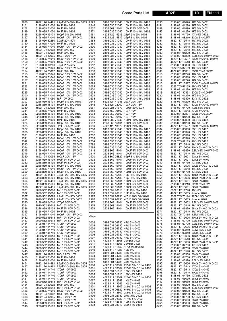
Spare Parts List EN 111A02E 10.
2088 4822 126 14491 2.2µF -20+80% 10V 08052101 3198 035 71030 10nF 16V 04022102 3198 035 71030 10nF 16V 04022119 3198 035 71030 10nF 16V 04022126 2238 869 15101 100pF 5% 50V 04022127 3198 035 71040 100nF 10% 16V 04022128 3198 030 82280 2.2µF 20% 50V2130 3198 035 71030 10nF 16V 04022134 3198 035 71040 100nF 10% 16V 04022135 4822 124 23002 10µF 20% 16V2136 4822 124 23002 10µF 20% 16V2137 4822 124 12095 100µF 20% 16V2138 3198 035 71040 100nF 10% 16V 04022150 3198 035 71040 100nF 10% 16V 04022151 3198 030 82280 2.2µF 20% 50V2152 3198 035 71040 100nF 10% 16V 04022154 4822 124 23002 10µF 20% 16V2155 3198 035 71040 100nF 10% 16V 04022156 3198 035 71040 100nF 10% 16V 04022157 3198 035 71040 100nF 10% 16V 04022281 3198 035 71040 100nF 10% 16V 04022282 3198 035 71040 100nF 10% 16V 04022284 3198 035 71040 100nF 10% 16V 04022285 3198 035 71040 100nF 10% 16V 04022300 3198 035 71040 100nF 10% 16V 04022305 3198 017 41050 1µF 10V 06032307 2238 869 15101 100pF 5% 50V 04022308 2238 869 15101 100pF 5% 50V 04022310 4822 124 23002 10µF 20% 16V2311 3198 035 71030 10nF 16V 04022317 2238 869 15101 100pF 5% 50V 04022318 2238 869 15101 100pF 5% 50V 04022321 3198 035 71030 10nF 16V 04022324 2238 869 15101 100pF 5% 50V 04022325 2238 869 75829 82pF 5% 50V 04022327 2238 869 15101 100pF 5% 50V 04022328 2238 869 15101 100pF 5% 50V 04022331 3198 035 71030 10nF 16V 04022341 3198 035 71040 100nF 10% 16V 04022342 3198 035 71040 100nF 10% 16V 04022343 3198 035 71040 100nF 10% 16V 04022344 3198 035 71040 100nF 10% 16V 04022345 3198 035 71040 100nF 10% 16V 04022346 3198 035 71040 100nF 10% 16V 04022350 4822 124 12095 100µF 20% 16V2351 2238 869 15109 10pF 5% 50V 04022352 2238 869 15109 10pF 5% 50V 04022358 2238 869 15101 100pF 5% 50V 04022359 3198 035 71040 100nF 10% 16V 04022360 2238 869 15101 100pF 5% 50V 04022361 4822 126 14491 2.2µF -20+80% 10V 08052363 2238 869 15101 100pF 5% 50V 04022364 4822 126 14491 2.2µF -20+80% 10V 08052365 2238 869 15101 100pF 5% 50V 04022366 4822 126 14491 2.2µF -20+80% 10V 08052371 2020 552 96618 1nF 10% 50V 04022372 2020 552 96618 1nF 10% 50V 04022377 2020 552 96623 2.2nF 10% 50V 04022379 2020 552 96623 2.2nF 10% 50V 04022380 3198 035 04710 470pF 50V 04022384 2020 552 96618 1nF 10% 50V 04022386 2238 869 15109 10pF 5% 50V 04022395 3198 035 71030 10nF 16V 04022397 3198 035 71040 100nF 10% 16V 04022432 2020 552 96618 1nF 10% 50V 04022433 2020 552 96618 1nF 10% 50V 04022434 3198 017 44740 470nF 10V 06032435 3198 017 44740 470nF 10V 06032438 3198 017 44740 470nF 10V 06032439 3198 017 44740 470nF 10V 06032440 2020 552 96618 1nF 10% 50V 04022441 2020 552 96618 1nF 10% 50V 04022442 2020 552 96618 1nF 10% 50V 04022443 2020 552 96618 1nF 10% 50V 04022444 2020 552 96618 1nF 10% 50V 04022445 2020 552 96618 1nF 10% 50V 04022447 4822 124 12095 100µF 20% 16V2450 3198 035 71030 10nF 16V 04022452 3198 035 71030 10nF 16V 04022454 4822 126 14491 2.2µF -20+80% 10V 08052457 4822 126 14491 2.2µF -20+80% 10V 08052461 3198 017 44740 470nF 10V 06032462 3198 017 44740 470nF 10V 06032480 3198 017 44740 470nF 10V 06032481 3198 017 44740 470nF 10V 06032483 2020 552 96618 1nF 10% 50V 04022484 4822 124 23002 10µF 20% 16V2485 2020 552 96618 1nF 10% 50V 04022486 3198 035 71040 100nF 10% 16V 04022487 4822 124 23002 10µF 20% 16V2488 4822 124 12095 100µF 20% 16V2489 4822 124 12095 100µF 20% 16V2514 2238 869 15189 18pF 5% 50V 04022516 2238 869 15189 18pF 5% 50V 0402
2525 3198 035 71040 100nF 10% 16V 04022546 3198 035 71040 100nF 10% 16V 04022557 2238 869 15101 100pF 5% 50V 04022571 3198 035 71040 100nF 10% 16V 04022581 4822 126 14519 22pF 5% 50V 04022582 4822 126 14519 22pF 5% 50V 04022583 3198 035 71040 100nF 10% 16V 04022584 3198 035 71040 100nF 10% 16V 04022600 3198 035 71040 100nF 10% 16V 04022601 3198 035 71040 100nF 10% 16V 04022604 3198 035 71040 100nF 10% 16V 04022607 3198 035 71040 100nF 10% 16V 04022609 3198 035 71040 100nF 10% 16V 04022611 3198 035 71040 100nF 10% 16V 04022612 3198 035 71040 100nF 10% 16V 04022615 3198 035 71040 100nF 10% 16V 04022618 3198 035 71040 100nF 10% 16V 04022620 3198 035 71040 100nF 10% 16V 04022622 3198 035 71040 100nF 10% 16V 04022623 3198 035 71040 100nF 10% 16V 04022628 3198 035 71040 100nF 10% 16V 04022629 3198 035 71040 100nF 10% 16V 04022630 3198 035 71040 100nF 10% 16V 04022633 3198 035 71040 100nF 10% 16V 04022634 3198 035 71040 100nF 10% 16V 04022638 3198 035 71040 100nF 10% 16V 04022644 5322 124 41945 22µF 20% 35V2645 4822 124 23002 10µF 20% 16V2651 2020 021 91679 100µF 20% 6.3V2652 2020 552 96507 10µF 10V2654 2020 552 96507 10µF 10V2655 2020 552 96507 10µF 10V2656 3198 035 71040 100nF 10% 16V 04022657 2238 869 15101 100pF 5% 50V 04022659 4822 126 13879 220nF 20% 16V2730 3198 035 71040 100nF 10% 16V 04022731 3198 035 71040 100nF 10% 16V 04022732 3198 035 71040 100nF 10% 16V 04022733 3198 035 71040 100nF 10% 16V 04022734 3198 035 71040 100nF 10% 16V 04022792 3198 035 71040 100nF 10% 16V 04022793 3198 035 71040 100nF 10% 16V 04022918 2238 869 15101 100pF 5% 50V 04022919 2238 869 15101 100pF 5% 50V 04022920 2238 869 75829 82pF 5% 50V 04022932 2238 869 15101 100pF 5% 50V 04022933 2238 869 15101 100pF 5% 50V 04022935 2238 869 15101 100pF 5% 50V 04022936 2238 869 15101 100pF 5% 50V 04022938 2238 869 15101 100pF 5% 50V 04022948 2238 869 15189 18pF 5% 50V 04022949 2238 869 15189 18pF 5% 50V 04022950 2238 869 15101 100pF 5% 50V 04022951 2238 869 15101 100pF 5% 50V 04022962 2238 869 15101 100pF 5% 50V 04022967 2020 552 96618 1nF 10% 50V 04022968 2020 552 96618 1nF 10% 50V 04022975 2020 552 96793 4.7nF 10% 50V 04022976 2020 552 96793 4.7nF 10% 50V 04022977 2238 869 15101 100pF 5% 50V 04022978 2238 869 15101 100pF 5% 50V 04022979 2238 869 15101 100pF 5% 50V 0402
3002 3198 031 04730 47Ω 5% 04023003 3198 031 04730 47Ω 5% 04023004 3198 031 04730 47Ω 5% 04023005 3198 031 04730 47Ω 5% 04023006 3198 031 04730 47Ω 5% 04023007 3198 031 04730 47Ω 5% 04023010 4822 117 13605 Jumper 04023011 4822 117 13605 Jumper 04023018 4822 117 11152 4.7Ω 5% 0.062W3019 5322 117 11726 10Ω 5%3022 3198 031 04730 47Ω 5% 04023024 3198 031 04730 47Ω 5% 04023026 3198 031 04730 47Ω 5% 04023027 3198 031 04730 47Ω 5% 04023060 4822 117 13602 2.2kΩ 5% 0.01W 04023061 4822 117 13602 2.2kΩ 5% 0.01W 04023062 3198 031 01810 180Ω 5% 04023063 3198 031 01810 180Ω 5% 04023066 4822 117 13602 2.2kΩ 5% 0.01W 04023067 4822 117 13548 1kΩ 5% 04023068 4822 117 13548 1kΩ 5% 04023101 4822 117 13602 2.2kΩ 5% 0.01W 04023103 3198 031 06820 6.8kΩ 5% 0.01W 04023104 4822 117 13602 2.2kΩ 5% 0.01W 04023106 3198 031 02730 27kΩ 5% 04023131 3198 031 04720 4.7kΩ 5% 04023132 4822 117 13545 100Ω 1% 04023138 3198 031 03910 390Ω 1% 0402
3150 3198 031 01820 1K8 5% 04023151 3198 031 01220 1K2 5% 04023152 3198 031 01820 1K8 5% 04023153 3198 031 01220 1K2 5% 04023154 3198 031 04730 47Ω 5% 04023155 3198 031 08210 820Ω 5% 0,5W3281 4822 117 13548 1kΩ 5% 04023282 4822 117 13548 1kΩ 5% 04023283 4822 117 13548 1kΩ 5% 04023284 4822 117 13548 1kΩ 5% 04023302 3198 031 01220 1K2 5% 04023303 3198 031 06820 6.8kΩ 5% 0.01W 04023304 4822 117 13597 330Ω 5% 0402 0.01W3305 4822 117 13548 1kΩ 5% 04023306 3198 031 03390 33Ω 1% 04023307 2322 705 87189 18Ω 5% 04023309 4822 051 30331 330Ω 5% 0.062W3310 3198 031 01220 1K2 5% 04023311 3198 031 03390 33Ω 1% 04023312 3198 031 01220 1K2 5% 04023313 4822 117 13597 330Ω 5% 0402 0.01W3316 2322 705 87189 18Ω 5% 04023318 3198 031 01220 1K2 5% 04023319 4822 051 30331 330Ω 5% 0.062W3320 3198 031 01220 1K2 5% 04023321 3198 031 03390 33Ω 1% 04023322 3198 031 01220 1K2 5% 04023323 4822 117 13597 330Ω 5% 0402 0.01W3325 3198 031 04720 4.7kΩ 5% 04023326 4822 117 13543 470Ω 5% 04023329 4822 051 30331 330Ω 5% 0.062W3330 3198 031 01220 1K2 5% 04023331 3198 031 03390 33Ω 1% 04023332 3198 031 01220 1K2 5% 04023333 4822 117 13597 330Ω 5% 0402 0.01W3334 3198 031 03390 33Ω 1% 04023335 3198 031 03390 33Ω 1% 04023336 3198 031 03390 33Ω 1% 04023337 3198 031 03390 33Ω 1% 04023338 2322 705 87189 18Ω 5% 04023340 4822 117 13548 1kΩ 5% 04023343 4822 117 13606 10kΩ 5% 0.01W 04023345 3198 031 06820 6.8kΩ 5% 0.01W 04023346 4822 117 13548 1kΩ 5% 04023347 4822 117 13601 22kΩ 5% 04023348 4822 117 13601 22kΩ 5% 04023349 3198 031 04730 47Ω 5% 04023350 4822 117 13596 220Ω 5% 0.01W 04023351 4822 117 13548 1kΩ 5% 04023352 3198 031 04730 47Ω 5% 04023353 4822 117 13606 10kΩ 5% 0.01W 04023354 4822 117 13606 10kΩ 5% 0.01W 04023355 4822 117 13601 22kΩ 5% 04023356 3198 031 08210 820Ω 5% 0,5W3357 4822 117 13601 22kΩ 5% 04023358 5322 117 11726 10Ω 5%3361 4822 117 13605 Jumper 04023364 2322 705 70124 120kΩ 5% 04023365 4822 117 13605 Jumper 04023366 4822 117 13602 2.2kΩ 5% 0.01W 04023367 4822 117 13548 1kΩ 5% 04023368 3198 031 06830 68kΩ 5% 0.01W 04023371 4822 117 13548 1kΩ 5% 04023372 2322 705 70155 1.5MΩ 5% 04023373 4822 117 13606 10kΩ 5% 0.01W 04023374 3198 031 02720 2.7kΩ 5% 0.01W 04023375 3198 031 02720 2.7kΩ 5% 0.01W 04023376 4822 117 13606 10kΩ 5% 0.01W 04023377 3198 031 02250 2.2MΩ 5% 04023378 3198 031 03340 330kΩ 5% 04023380 4822 117 13606 10kΩ 5% 0.01W 04023382 4822 117 13548 1kΩ 5% 04023384 4822 117 13606 10kΩ 5% 0.01W 04023385 3198 031 04730 47Ω 5% 04023386 3198 031 02730 27kΩ 5% 04023390 4822 117 13548 1kΩ 5% 04023391 3198 031 03930 39kΩ 5% 04023392 3198 031 04730 47Ω 5% 04023393 3198 031 03320 3.3kΩ 5% 04023395 4822 117 13606 10kΩ 5% 0.01W 04023396 4822 117 13543 470Ω 5% 04023397 4822 117 13543 470Ω 5% 04023398 4822 117 13545 100Ω 1% 04023445 3198 031 04730 47Ω 5% 04023446 3198 031 05630 56kΩ 5% 04023447 3198 031 05630 56kΩ 5% 04023448 3198 031 01220 1K2 5% 04023449 3198 031 01520 1.2kΩ 5% 0.01W 04023450 3198 031 01220 1K2 5% 04023452 3198 031 01220 1K2 5% 04023453 3198 031 04730 47Ω 5% 04023454 3198 031 05630 56kΩ 5% 04023455 3198 031 05630 56kΩ 5% 04023456 3198 031 01220 1K2 5% 0402

Spare Parts ListEN 112 A02E10.
3457 3198 031 01520 1.2kΩ 5% 0.01W 04023480 3198 031 02720 2.7kΩ 5% 0.01W 04023481 3198 031 02720 2.7kΩ 5% 0.01W 04023482 3198 031 04720 4.7kΩ 5% 04023483 3198 031 08220 8.2kΩ 5% 0.5W3484 3198 031 04720 4.7kΩ 5% 04023485 3198 031 08220 8.2kΩ 5% 0.5W3501 4822 117 13606 10kΩ 5% 0.01W 04023502 4822 117 13606 10kΩ 5% 0.01W 04023503 4822 117 13606 10kΩ 5% 0.01W 04023504 4822 117 13606 10kΩ 5% 0.01W 04023507 4822 117 13606 10kΩ 5% 0.01W 04023508 3198 031 04720 4.7kΩ 5% 04023509 3198 031 02720 2.7kΩ 5% 0.01W 04023510 3198 031 02720 2.7kΩ 5% 0.01W 04023511 4822 117 13546 47Ω 5% 04023512 4822 117 13546 47Ω 5% 04023513 3198 031 02720 2.7kΩ 5% 0.01W 04023515 3198 031 02720 2.7kΩ 5% 0.01W 04023518 4822 117 13601 22kΩ 5% 04023523 4822 117 13606 10kΩ 5% 0.01W 04023530 4822 117 11297 100kΩ 5% 0.1W3547 3198 031 03390 33Ω 1% 04023550 3198 031 04720 4.7kΩ 5% 04023557 4822 117 13546 47Ω 5% 04023563 4822 117 13606 10kΩ 5% 0.01W 04023564 4822 117 13606 10kΩ 5% 0.01W 04023565 4822 117 13606 10kΩ 5% 0.01W 04023570 4822 117 13602 2.2kΩ 5% 0.01W 04023571 3198 031 02720 2.7kΩ 5% 0.01W 04023572 4822 117 13606 10kΩ 5% 0.01W 04023581 4822 117 13545 100Ω 1% 04023582 4822 117 13606 10kΩ 5% 0.01W 04023583 3198 031 01830 18kΩ 5% 0.01W 04023586 4822 117 13601 22kΩ 5% 04023590 4822 117 13548 1kΩ 5% 04023651 5322 117 13036 1.2kΩ 1% 0.063W 06033652 5322 117 13052 2.7kΩ 1% 0.063W 06033737 3198 031 03390 33Ω 1% 04023904 4822 117 13605 Jumper 04023909 4822 117 13545 100Ω 1% 04023911 4822 117 13545 100Ω 1% 04023918 4822 117 13545 100Ω 1% 04023919 4822 117 13545 100Ω 1% 04023928 4822 117 13545 100Ω 1% 04023929 4822 117 13545 100Ω 1% 04023936 4822 117 13545 100Ω 1% 04023938 4822 117 13545 100Ω 1% 04023950 4822 117 13545 100Ω 1% 04023951 4822 117 13545 100Ω 1% 04023962 4822 117 13545 100Ω 1% 04023963 4822 117 13545 100Ω 1% 04023964 4822 117 13545 100Ω 1% 04023975 4822 117 13545 100Ω 1% 04023976 4822 117 13545 100Ω 1% 04023977 4822 117 13545 100Ω 1% 04023978 4822 117 13545 100Ω 1% 04023979 4822 117 13545 100Ω 1% 04023980 4822 117 13545 100Ω 1% 04024xxx 4822 117 13605 Jumper 0402
5060 2422 549 44197 Bead 220Ω at 100MHz5061 2422 549 44197 Bead 220Ω at 100MHz5062 2422 549 44197 Bead 220Ω at 100MHz5063 2422 549 44197 Bead 220Ω at 100MHz5101 4822 157 71303 0.39µH 10% 08055102 2422 549 44197 Bead 220Ω at 100MHz5112 2422 549 44197 Bead 220Ω at 100MHz5134 2422 549 44197 Bead 220Ω at 100MHz5135 2422 549 44197 Bead 220Ω at 100MHz5150 2422 549 44197 Bead 220Ω at 100MHz5151 2422 549 44197 Bead 220Ω at 100MHz5152 2422 549 44197 Bead 220Ω at 100MHz5281 2422 549 44197 Bead 220Ω at 100MHz5282 2422 549 44197 Bead 220Ω at 100MHz5283 2422 549 44197 Bead 220Ω at 100MHz5285 2422 549 44197 Bead 220Ω at 100MHz5300 2422 549 44197 Bead 220Ω at 100MHz5307 4822 051 20008 Jumper 08055317 4822 051 20008 Jumper 08055327 4822 051 20008 Jumper 08055328 4822 051 20008 Jumper 08055342 2422 549 44197 Bead 220Ω at 100MHz5343 2422 549 44197 Bead 220Ω at 100MHz5344 2422 549 44197 Bead 220Ω at 100MHz5345 2422 549 44197 Bead 220Ω at 100MHz5450 2422 549 44197 Bead 220Ω at 100MHz5452 2422 549 44197 Bead 220Ω at 100MHz5480 2422 549 44197 Bead 220Ω at 100MHz5570 2422 549 44197 Bead 220Ω at 100MHz5583 2422 549 44197 Bead 220Ω at 100MHz
5600 4822 157 11716 Bead 30Ω at 100MHz5601 2422 549 44197 Bead 220Ω at 100MHz5651 2422 535 94134 10µH 20% 08055654 4822 157 11258 1µH 20% NLC322522T5659 4822 157 71334 0.68µH5730 2422 549 44197 Bead 220Ω at 100MHz5731 2422 549 44197 Bead 220Ω at 100MHz5792 2422 549 44197 Bead 220Ω at 100MHz
6101 4822 130 11525 1SS3566301 4822 130 11397 BAS3166327 9322 102 64685 UDZ2.7B6341 4822 130 11397 BAS3166353 5322 130 34337 BAV996365 5322 130 34337 BAV996367 9340 548 67115 PDZ22B6368 4822 130 11397 BAS3166381 5322 130 34337 BAV996382 4822 130 11594 BZX284-C476384 9340 548 67115 PDZ22B6385 4822 130 11397 BAS3166397 9340 548 69115 PDZ27B6398 4822 130 11397 BAS3166480 9340 548 61115 PDZ12B6481 9340 548 61115 PDZ12B6651 9322 128 70685 SMSS14
7060 9340 425 30115 BC847BPN7062 4822 130 60373 BC856B7063 4822 130 60373 BC856B7100 9352 712 54557 PNX3000HL/N17101 3198 010 42310 BC847BW7150 9340 425 20115 BC847BS7300 9352 735 54557 PNX3002E/N3027301 4822 130 60373 BC856B7302 4822 130 60373 BC856B7303 4822 130 60373 BC856B7304 3198 010 42310 BC847BW7310 9340 425 30115 BC847BPN7320 9340 425 30115 BC847BPN7330 9340 425 30115 BC847BPN7346 4822 130 60373 BC856B7356 4822 130 60373 BC856B7365 5322 130 60159 BC846B7382 4822 130 60373 BC856B7383 9340 425 30115 BC847BPN7393 3198 010 42310 BC847BW7432 9340 425 30115 BC847BPN7433 9340 425 30115 BC847BPN7480 4822 209 33165 TDA1308T/N17525 9322 130 41668 M24C64-WMN67581 9352 691 56115 NE56610-45GW7650 9322 170 61668 CS51033YDR87651 9322 170 87668 STS5PF30L7730 9322 180 88668 K4S641632F-TC757790 9322 199 76668 M58LW032C90N1
Side I/O Panel [D]
Various
0240 2422 025 12485 Connector 11p m0241 4822 267 10734 Connector 5p m0242 4822 267 10734 Connector 5p m1254 4822 267 31014 Socket headphone1255 4822 265 11606 Connector 3p1256 2422 026 04926 Socket SVHS 4p f
2286 4822 122 33642 150pF 5% 50V2288 4822 122 33642 150pF 5% 50V2292 5322 122 32311 470pF 10% 100V2294 5322 122 32311 470pF 10% 100V2296 4822 122 30103 22nF 80% 63V2297 4822 122 30103 22nF 80% 63V
3285 4822 116 52201 75Ω 5% 0.5W3286 4822 116 52176 10Ω 5% 0.5W3287 4822 116 52201 75Ω 5% 0.5W3288 4822 116 52176 10Ω 5% 0.5W3289 4822 116 52249 1.8kΩ 5% 0.5W3291 4822 050 11002 1kΩ 1% 0.4W3292 4822 117 10834 47kΩ 1% 0.1W
3293 4822 050 11002 1kΩ 1% 0.4W3294 4822 117 10834 47kΩ 1% 0.1W3295 4822 116 52276 3.9kΩ 5% 0.5W3296 4822 117 10833 10kΩ 1% 0.1W3297 4822 117 10833 10kΩ 1% 0.1W4xxx 4822 051 20008 Jumper 0805
6291 9340 548 61115 PDZ12B6292 9340 548 61115 PDZ12B6293 9340 548 61115 PDZ12B6294 9340 548 61115 PDZ12B6296 9340 548 61115 PDZ12B6297 9340 548 61115 PDZ12B
Top Control Panel [E]
Various
0135 3104 311 04671 Cable 3p/1200/3p0215 2422 025 16601 Connector 3p m1091 4822 276 13775 Switch1092 4822 276 13775 Switch1093 4822 276 13775 Switch1094 4822 276 13775 Switch
2010 4822 122 33177 10nF 20% 50V
3088 4822 051 30008 Jumper 06033089 4822 051 30008 Jumper 06033091 4822 051 30561 560Ω 5% 0.062W3092 4822 051 30391 390Ω 5% 0.062W3093 4822 051 30561 560Ω 5% 0.062W3094 4822 051 30271 270Ω 5% 0.062W3095 4822 051 30332 3.3kΩ 5% 0.062W3096 4822 051 30152 1.5kΩ 5% 0.062W4092 4822 051 30008 Jumper 0603
6092 4822 130 10654 BAT254
CRT Panel [F]
Various
0032 4822 492 70788 IC clamp1298 2422 500 80063 Connector CRT 10p f1424 2422 025 11244 Connector 7p m1434 4822 267 10973 Connector 1p m1483 4822 267 10735 Connector 3p m1940 2422 025 12485 Connector 11p m8483 3104 311 03111 Cable 3p/340/3p ferrite
2300 4822 124 40764 22µF 100 V2301 4822 124 40196 220µF 20% 16V2304 4822 121 41856 22nF 5% 250V2306 2238 586 59812 100nF 20-80% 50V 06032307 4822 121 41856 22nF 5% 250V2309 3198 017 42230 22nF 50V2313 4822 124 12373 47µF 20% 250V2315 5322 126 11583 10nF 10% 50V 06032316 4822 121 40518 100nF 10% 250V2318 5322 122 32654 22nF 10% 63V2319 4822 122 30043 10nF 80% 63V2320 2238 586 59812 100nF 20-80% 50V 06032324 5322 121 44356 4.7nF 5% 2kV2325 2238 586 59812 100nF 20-80% 50V 06032330 4822 126 13879 220nF 20% 16V2338 2238 786 19856 330nF 16V 06032409 4822 051 30008 Jumper 06032410 3198 017 44740 470nF 10V 06032411 4822 126 14585 100nF 10% 50V2420 4822 051 30008 Jumper 0603
3300 4822 052 10109 10Ω 5% 0.33W3301 4822 053 12103 10K00 5% 3W3302 4822 051 30681 680Ω 5% 0.062W
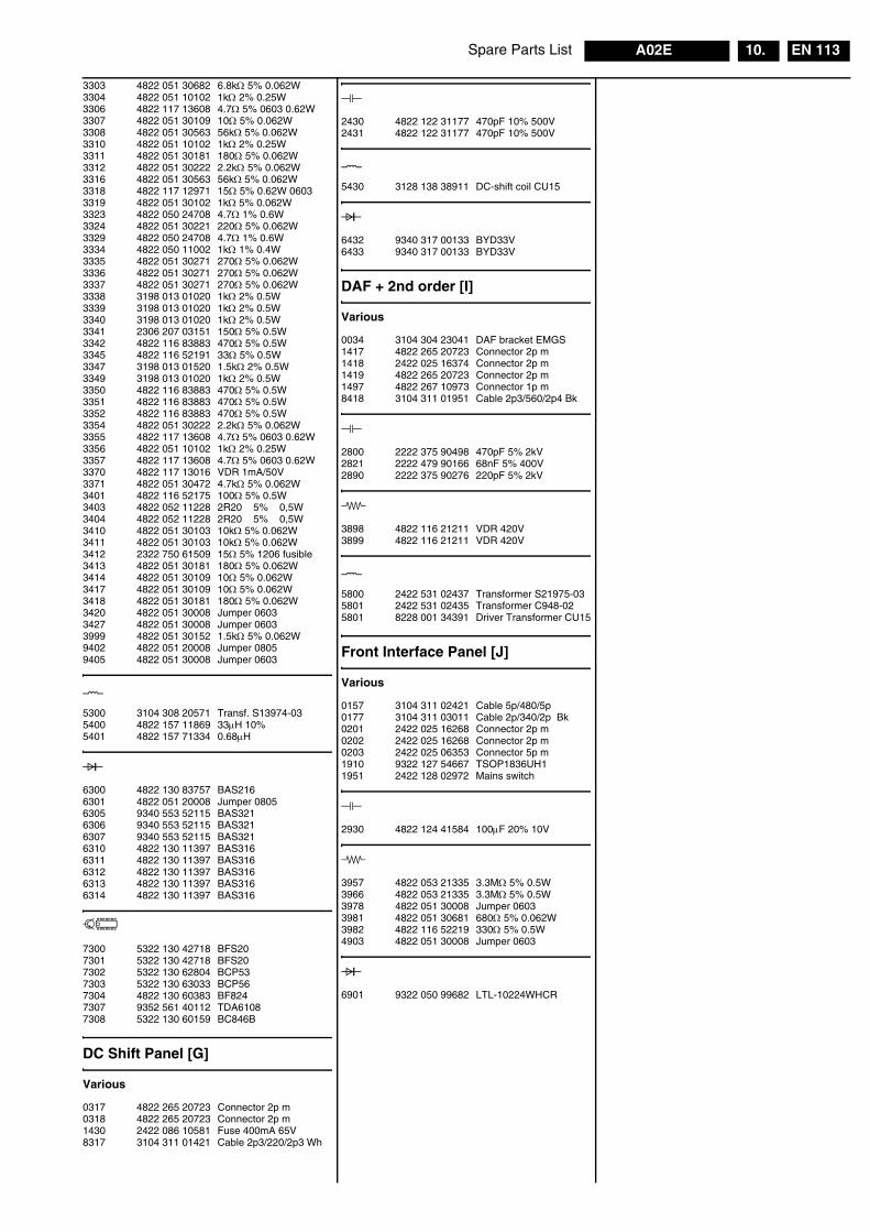
Spare Parts List EN 113A02E 10.
3303 4822 051 30682 6.8kΩ 5% 0.062W3304 4822 051 10102 1kΩ 2% 0.25W3306 4822 117 13608 4.7Ω 5% 0603 0.62W3307 4822 051 30109 10Ω 5% 0.062W3308 4822 051 30563 56kΩ 5% 0.062W3310 4822 051 10102 1kΩ 2% 0.25W3311 4822 051 30181 180Ω 5% 0.062W3312 4822 051 30222 2.2kΩ 5% 0.062W3316 4822 051 30563 56kΩ 5% 0.062W3318 4822 117 12971 15Ω 5% 0.62W 06033319 4822 051 30102 1kΩ 5% 0.062W3323 4822 050 24708 4.7Ω 1% 0.6W3324 4822 051 30221 220Ω 5% 0.062W3329 4822 050 24708 4.7Ω 1% 0.6W3334 4822 050 11002 1kΩ 1% 0.4W3335 4822 051 30271 270Ω 5% 0.062W3336 4822 051 30271 270Ω 5% 0.062W3337 4822 051 30271 270Ω 5% 0.062W3338 3198 013 01020 1kΩ 2% 0.5W3339 3198 013 01020 1kΩ 2% 0.5W3340 3198 013 01020 1kΩ 2% 0.5W3341 2306 207 03151 150Ω 5% 0.5W3342 4822 116 83883 470Ω 5% 0.5W3345 4822 116 52191 33Ω 5% 0.5W3347 3198 013 01520 1.5kΩ 2% 0.5W3349 3198 013 01020 1kΩ 2% 0.5W3350 4822 116 83883 470Ω 5% 0.5W3351 4822 116 83883 470Ω 5% 0.5W3352 4822 116 83883 470Ω 5% 0.5W3354 4822 051 30222 2.2kΩ 5% 0.062W3355 4822 117 13608 4.7Ω 5% 0603 0.62W3356 4822 051 10102 1kΩ 2% 0.25W3357 4822 117 13608 4.7Ω 5% 0603 0.62W3370 4822 117 13016 VDR 1mA/50V3371 4822 051 30472 4.7kΩ 5% 0.062W3401 4822 116 52175 100Ω 5% 0.5W3403 4822 052 11228 2R20 5% 0,5W3404 4822 052 11228 2R20 5% 0,5W3410 4822 051 30103 10kΩ 5% 0.062W3411 4822 051 30103 10kΩ 5% 0.062W3412 2322 750 61509 15Ω 5% 1206 fusible3413 4822 051 30181 180Ω 5% 0.062W3414 4822 051 30109 10Ω 5% 0.062W3417 4822 051 30109 10Ω 5% 0.062W3418 4822 051 30181 180Ω 5% 0.062W3420 4822 051 30008 Jumper 06033427 4822 051 30008 Jumper 06033999 4822 051 30152 1.5kΩ 5% 0.062W9402 4822 051 20008 Jumper 08059405 4822 051 30008 Jumper 0603
5300 3104 308 20571 Transf. S13974-035400 4822 157 11869 33µH 10%5401 4822 157 71334 0.68µH
6300 4822 130 83757 BAS2166301 4822 051 20008 Jumper 08056305 9340 553 52115 BAS3216306 9340 553 52115 BAS3216307 9340 553 52115 BAS3216310 4822 130 11397 BAS3166311 4822 130 11397 BAS3166312 4822 130 11397 BAS3166313 4822 130 11397 BAS3166314 4822 130 11397 BAS316
7300 5322 130 42718 BFS207301 5322 130 42718 BFS207302 5322 130 62804 BCP537303 5322 130 63033 BCP567304 4822 130 60383 BF8247307 9352 561 40112 TDA61087308 5322 130 60159 BC846B
DC Shift Panel [G]
Various
0317 4822 265 20723 Connector 2p m0318 4822 265 20723 Connector 2p m1430 2422 086 10581 Fuse 400mA 65V8317 3104 311 01421 Cable 2p3/220/2p3 Wh
2430 4822 122 31177 470pF 10% 500V2431 4822 122 31177 470pF 10% 500V
5430 3128 138 38911 DC-shift coil CU15
6432 9340 317 00133 BYD33V6433 9340 317 00133 BYD33V
DAF + 2nd order [I]
Various
0034 3104 304 23041 DAF bracket EMGS1417 4822 265 20723 Connector 2p m1418 2422 025 16374 Connector 2p m1419 4822 265 20723 Connector 2p m1497 4822 267 10973 Connector 1p m8418 3104 311 01951 Cable 2p3/560/2p4 Bk
2800 2222 375 90498 470pF 5% 2kV2821 2222 479 90166 68nF 5% 400V2890 2222 375 90276 220pF 5% 2kV
3898 4822 116 21211 VDR 420V3899 4822 116 21211 VDR 420V
5800 2422 531 02437 Transformer S21975-035801 2422 531 02435 Transformer C948-025801 8228 001 34391 Driver Transformer CU15
Front Interface Panel [J]
Various
0157 3104 311 02421 Cable 5p/480/5p0177 3104 311 03011 Cable 2p/340/2p Bk0201 2422 025 16268 Connector 2p m0202 2422 025 16268 Connector 2p m0203 2422 025 06353 Connector 5p m1910 9322 127 54667 TSOP1836UH11951 2422 128 02972 Mains switch
2930 4822 124 41584 100µF 20% 10V
3957 4822 053 21335 3.3MΩ 5% 0.5W3966 4822 053 21335 3.3MΩ 5% 0.5W3978 4822 051 30008 Jumper 06033981 4822 051 30681 680Ω 5% 0.062W3982 4822 116 52219 330Ω 5% 0.5W4903 4822 051 30008 Jumper 0603
6901 9322 050 99682 LTL-10224WHCR


![philips tv chasis L03[1][1][1].2L AA](https://img.pdfslide.net/doc/110x75/54e9955e4a795910478b468e/philips-tv-chasis-l031112l-aa.jpg)

![PHILIPS PDP Ch. LC4.41E AA[1]](https://img.pdfslide.net/doc/110x75/551eedde497959cf398b4d89/philips-pdp-ch-lc441e-aa1.jpg)