Embed Size (px)
Citation preview

ALL RIGHTS ARE STRICTLY RESERVED. ANY PORTION OF THIS PAPER SHALL NOT BE REPRODUCED, COPIED, OR TRANSLATED TO ANY OTHER FORMS WITHOUT PERMISSION FROM PHISON ELECTRONICS
CORPORATION.
Phison Electronics Corporation
TLC microSD 3.0 Memory Card Specification
(UHS-I)
Version 1.9
Document Number: S-14346
No.1, Qun-Yi Road, Jhunan, Miaoli County, Taiwan 350, R.O.C Tel: +886-37-586-896 Fax: +886-37-587-868 E-mail : [email protected] /

TLC microSD Card (UHS-I)
Revision History
Revision History Draft Date Remark
1.0 First release 2013/12/23 Yvonne
1.1 Add new configuration 2014/04/03 Lucas
1.2 Modify temperature range 2014/04/08 Lucas
1.3 Modify configuration & Modify power consumption 2014/05/19 Lucas
1.4 Modify power consumption 2014/05/21 Lucas
1.5 Add note in Temperature and Humidity 2014/05/22 Lucas
1.6 Modify absolute maximum rating 2014/06/03 Lucas
1.7 Add new configuration 2014/06/26 Lucas
1.8 1. Modify performance overview
2. Add Table 4-2
2014/07/17 Lucas
1.9 1. Modify performance overview
2. Add note in card capacitance for each signal pin
3. Add note in tIH of SDR50 and SDR104 input timing
2014/07/24 Lucas

TLC microSD Card (UHS-I)
Overview
Flash Type
Toshiba 19nm TLC
Toshiba A19nm TLC
Bus Speed Mode
UHS-I
Speed Class
Class 2/4/6/10
Power Consumption Note
Power Up Current < 250uA
Standby Current < 1000uA
Read Current < 400mA
Write Current < 400mA
CPRM (Content Protection for Recordable
Media)
Advanced Flash Management
Static and Dynamic Wear Leveling
Bad Block Management
Write Protect with mechanical switch
Supply Voltage 2.7 ~ 3.6V
Temperature Range
Operation: 0°C ~ 70°C
Storage: -25°C ~ 85°C
RoHS compliant
EMI compliant
NOTE: Please see Chapter 5.1 Power Consumption for details.

TLC microSD Card (UHS-I)
Performance Overview
Capacity Class UHS-I Controller
Flash
(Bit-per-cell: TLC)
HDBenchWINXP
(@1000MB) Kbytes
TestMetrix Test
Test 500MB
Density Process Read
(KB/s)
Write
(KB/s)
Read
(MB/s)
Write
(MB/s)
4GB CL4 UHS-I PS8035 32Gb*1 19nm 25,323 5,016 30.00 5.39
8GB CL4 UHS-I PS8035 64Gb*1 A19nm 28,864 4,823 30.13 5.19
16GB CL10 UHS-I
(Grade 1) PS8035 64Gb*2 A19nm 43,325 10,512 45.09 13.46
32GB CL10 UHS-I
(Grade 1) PS8035 64Gb*4 A19nm 41,888 13,000 45.55 13.75
64GB CL10 UHS-I
(Grade 1) PS8035 64Gb*8 A19nm 41,126 14,201 43.13 15.36
4GB CL4 UHS-I PS8037 32Gb*1 19nm 42,265 5,039 46.00 5.40
8GB CL4 UHS-I PS8037 64Gb*1 19nm 41,967 5,248 45.97 5.66
8GB CL4 UHS-I PS8037 64Gb*1 A19nm 43,325 4,839 46.00 5.26
16GB CL4 UHS-I PS8037 64Gb*2 A19nm 44.772 4.795 46.01 5.17
16GB CL10 UHS-I
(Grade 1) PS8210 64Gb*2 A19nm 79,367 12,234 83.73 13.34
32GB CL10 UHS-I
(Grade 1) PS8210 64Gb*4 A19nm 79,657 18,223 82.44 21.66
64GB CL10 UHS-I
(Grade 1) PS8210 64Gb*8 A19nm 78,515 19,914 87.05 22.04

TLC microSD Card (UHS-I)
Table of Contents
1. Introduction ................................................................................................ 1
1.1. General Description ......................................................................................................... 1
1.2. Flash Management ........................................................................................................... 1
1.2.1. Error Correction Code (ECC) .............................................................................. 1
1.2.2. Wear Leveling ...................................................................................................... 1
1.2.3. Bad Block Management ....................................................................................... 2
2. Product Specifications................................................................................. 3
3. Environmental Specifications ..................................................................... 4
3.1. Environmental Conditions ............................................................................................... 4
4. SD Card Comparison ................................................................................... 7
5. Electrical Specifications .............................................................................. 8
5.1. Power Consumption ......................................................................................................... 8
5.2. Absolute Maximum Rating .............................................................................................. 9
5.3. DC Characteristic ............................................................................................................. 9
5.3.1. Bus Operation Conditions for 3.3V Signaling ..................................................... 9
5.3.2. Bus Signal Line Load ......................................................................................... 10
5.3.3. Power Up Time .................................................................................................. 11
5.4. AC Characteristic ........................................................................................................... 12
5.4.1. microSD Interface Timing (Default) .................................................................. 12
5.4.2. microSD Interface Timing (High-Speed Mode) ................................................ 13
5.4.3. SD Interface Timing (SDR12, SDR25, SDR50 and SDR104 Modes) .............. 14
5.4.4. microSD Interface Timing (DDR50 Mode) ....................................................... 16
6. Interface .................................................................................................... 18
6.1. Pad Assignment and Descriptions.................................................................................. 18
7. Physical Dimension ................................................................................... 20

TLC microSD Card (UHS-I)
List of Tables
Table 3-1 High Temperature Test Condition ......................................................................................... 4
Table 3-2 Low Temperature Test Condition .......................................................................................... 4
Table 3-3 High Humidity Test Condition ............................................................................................... 4
Table 3-4 Temperature Cycle Test ........................................................................................................ 5
Table 3-5 Shock Specification ............................................................................................................... 5
Table 3-6 Vibration Specification ......................................................................................................... 5
Table 3-7 Drop Specification ................................................................................................................ 5
Table 3-8 Bending Specification ........................................................................................................... 5
Table 3-9 Torque Specification ............................................................................................................. 5
Table 3-10 Contact ESD Specification ................................................................................................... 6
Table 4-1 Comparing SD3.0 Standard, SD3.0 SDHC and SD3.0 SDXC ................................................... 7
Table 4-2 Comparing UHS Speed Grade Symbols ................................................................................ 7
Table 5-1 Power Consumption of microSD card .................................................................................. 8
Table 5-2 Threshold Level for High Voltage Range ............................................................................... 9
Table 5-3 Peak Voltage and Leakage Current ....................................................................................... 9
Table 5-4 Threshold Level for 1.8V Signaling ..................................................................................... 10
Table 5-5 Input Leakage Current for 1.8V Signaling ........................................................................... 10
Table 5-6 Clock Signal Timing ............................................................................................................. 14
Table 5-7 Output Timing of Fixed Data Window (SDR12, SDR25, SDR50 and SDR104 Modes) ......... 15
Table 5-8 Output Timing of Variable Window (SDR104) .................................................................... 16
Table 5-9 Bus Timings – Parameters Values (DDR50 Mode) .............................................................. 17
Table 6-1 microSD Memory Card Pad Assignment ............................................................................ 18

TLC microSD Card (UHS-I)
1
1. INTRODUCTION
1.1. General Description
The Micro Secure Digital (microSD) card version 3.0 is fully compliant with the standards released by the SD
Card Association. The Command List supports [Part 1 Physical Layer Specification Ver3.01 Final] definitions.
Card capacities of non-secure area and secure area support [Part 3 Security Specification Ver3.0 Final]
Specifications.
The microSD 3.0 card comes with an 8-pin interface, designed to operate at a maximum frequency of
208MHz. It can alternate communication protocol between the SD mode and SPI mode. It performs data
error detection and correction with very low power consumption. The Card capacity could be more than
64GB and up to 2TB in the future with ex-FAT file system, which is called SDXC (Extended Capacity SD
Memory Card).
Micro Secure Digital 3.0 cards are one of the most popular cards today due to its high performance, good
reliability and wide compatibility.
1.2. Flash Management
1.2.1. Error Correction Code (ECC)
Flash memory cells will deteriorate with use, which might generate random bit errors in the stored data.
Thus, microSD card applies the BCH ECC Algorithm, which can detect and correct errors occur during Read
process, ensure data been read correctly, as well as protect data from corruption.
1.2.2. Wear Leveling
NAND Flash devices can only undergo a limited number of program/erase cycles, and in most cases, the
flash media are not used evenly. If some area get updated more frequently than others, the lifetime of the
device would be reduced significantly. Thus, Wear Leveling technique is applied to extend the lifespan of
NAND Flash by evenly distributing write and erase cycles across the media.
Phison provides advanced Wear Leveling algorithm, which can efficiently spread out the flash usage through
the whole flash media area. Moreover, by implementing both dynamic and static Wear Leveling algorithms,
the life expectancy of the NAND Flash is greatly improved.
TLC microSD Card (UHS-I)
2
1.2.3. Bad Block Management
Bad blocks are blocks that include one or more invalid bits, and their reliability is not guaranteed. Blocks
that are identified and marked as bad by the manufacturer are referred to as “Initial Bad Blocks”. Bad blocks
that are developed during the lifespan of the flash are named “Later Bad Blocks”. Phison implements an
efficient bad block management algorithm to detect the factory-produced bad blocks and manages any bad
blocks that appear with use. This practice further prevents data being stored into bad blocks and improves
the data reliability.

TLC microSD Card (UHS-I)
3
2. PRODUCT SPECIFICATIONS
Support SD system specification version 3.0
Card capacity of non-secure area and secure area support [Part 3 Security Specification
Ver3.0 Final] Specifications
Support SD SPI mode
Designed for read-only and read/write cards
Bus Speed Mode (use 4 parallel data lines)
Non-UHS Mode
Default speed mode: 3.3V signaling, frequency up to 25MHz, up to 12.5 MB/sec
High speed mode: 3.3V signaling, frequency up to 50MHz, up to 25 MB/sec
UHS Mode
SDR12: SDR up to 25MHz, 1.8V signaling
SDR25: SDR up to 50MHz, 1.8V signaling
SDR50: 1.8V signaling, frequency up to 100MHz, up to 50 MB/sec
SDR104: 1.8V signaling, frequency up to 208MHz, up to 104MB/sec
DDR50: 1.8V signaling, frequency up to 50MHz, sampled on both clock edges, up to 50
MB/sec
NOTES: 1. Timing in 1.8V signaling is different from that of 3.3V signaling.
2. To properly run the UHS mode, please ensure the device supports UHS-I mode.
The command list supports [Part 1 Physical Layer Specification Ver3.1 Final] definitions
Copyrights Protection Mechanism
Compliant with the highest security of CPRM standard
Support CPRM (Content Protection for Recordable Media) of SD Card
Card removal during read operation will never harm the content
Password Protection of cards (optional)
Write Protect feature using mechanical switch
Built-in write protection features (permanent and temporary)
+4KV/-4KV ESD protection in contact pads
Operation voltage range: 2.7 ~ 3.6V
Support Dynamic and Static Wear Leveling
Dimension: 15mm (L) x 11mm (W) x 1mm (H)
TLC microSD Card (UHS-I)
4
3. ENVIRONMENTAL SPECIFICATIONS
3.1. Environmental Conditions
Temperature and Humidity
Temperature Range (NOTE)
Operational: 0°C ~ 70°C
Storage: -25°C ~ 85°C
NOTE: we suggest that customer use SD/micro SD card during the temperature range for better
reliability.
Humidity
Operational: RH = 93% under 25°C
Diamond grade: RH = 93% under 40°C
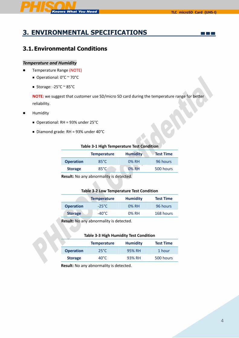
Table 3-1 High Temperature Test Condition
Temperature Humidity Test Time
Operation 85°C 0% RH 96 hours
Storage 85°C 0% RH 500 hours
Result: No any abnormality is detected.
Table 3-2 Low Temperature Test Condition
Temperature Humidity Test Time
Operation -25°C 0% RH 96 hours
Storage -40°C 0% RH 168 hours
Result: No any abnormality is detected.
Table 3-3 High Humidity Test Condition
Temperature Humidity Test Time
Operation 25°C 95% RH 1 hour
Storage 40°C 93% RH 500 hours
Result: No any abnormality is detected.

TLC microSD Card (UHS-I)
5
Table 3-4 Temperature Cycle Test
Temperature Test Time Cycle
Operation -25°C 30 min
10 Cycles 85°C 30 min
Storage -40°C 30 min
10 Cycles 85°C 30 min
Result: No any abnormality is detected.
Shock
Table 3-5 Shock Specification
Acceleration Force Half Sin Pulse Duration
microSD card 500G 2ms
Result: No any abnormality is detected when power on.
Vibration
Table 3-6 Vibration Specification
Condition Vibration Orientation
Frequency/Displacement Frequency/Acceleration
microSD card 20Hz~80Hz/1.52mm 80Hz~2000Hz/20G X, Y, Z axis/30 min for each
Result: No any abnormality is detected when power on.
Drop
Table 3-7 Drop Specification
Height of Drop Number of Drop
microSD card 150cm free fall 6 face of each unit
Result: No any abnormality is detected when power on.
Bending
Table 3-8 Bending Specification
Force Action
microSD card ≥ 10N Hold 1min/5 times
Result: No any abnormality is detected when power on.
Torque
Table 3-9 Torque Specification
Force Action
microSD card 0.1N-m or +/-2.5 deg Hold 30 seconds/5 times
Result: No any abnormality is detected when power on.
TLC microSD Card (UHS-I)
6
Electrostatic Discharge (ESD)
Table 3-10 Contact ESD Specification
Condition Result
microSD card Contact: +/- 4KV each item 5 times
Air: +/- 15KV 5 times PASS
EMI Compliance
FCC: CISPR22
CE: EN55022
BSMI 13438

TLC microSD Card (UHS-I)
7
4. SD CARD COMPARISON
Table 4-1 Comparing SD3.0 Standard, SD3.0 SDHC and SD3.0 SDXC
Table 4-2 Comparing UHS Speed Grade Symbols
*UHS (Ultra High Speed), the fastest performance category available today, defines bus-interface speeds up to 312 Megabytes per second for greater device performance. It is available on SDXC and SDHC memory cards and devices.
SD3.0 SDSC
(Backward compatible to 2.0
host)
SD3.0 SDHC
(Backward compatible to 2.0 host)
SD3.0 SDXC
File System FAT 12/16 FAT32 exFAT
Addressing Mode Byte
(1 byte unit)
Block
(512 byte unit)
Block
(512 byte unit)
HCS/CCS bits of ACMD41 Support Support Support
CMD8 (SEND_IF_COND) Support Support Support
CMD16 (SET_BLOCKLEN) Support Support
(Only CMD42)
Support
(Only CMD42)
Partial Read Support Not Support Not Support
Lock/Unlock Function Mandatory Mandatory Mandatory
Write Protect Groups Optional Not Support Not Support
Supply Voltage 2.7v – 3.6v
(for operation) Support Support Support
Total Bus Capacitance for each signal line
40pF 40pF 40pF
CSD Version
(CSD_STRUCTURE Value) 1.0 (0x0) 2.0 (0x1) 2.0 (0x1)
Speed Class Optional Mandatory
(Class 2 / 4 / 6 / 10)
Mandatory
(Class 2 / 4 / 6 / 10)
U1 ( UHS Speed Grade 1) U3 ( UHS Speed Grade 3)
Operable Under *UHS-I Bus I/F, UHS-II Bus I/F
SD Memory Card SDHC UHS-I and UHS-II, SDXC UHS-I and UHS-II
Mark
Performance 10 MB/s minimum write speed 30 MB/s minimum write speed
Applications
Full higher potential of recording real-time
broadcasts and capturing large-size HD videos.
Capable of recording 4K2K video.

TLC microSD Card (UHS-I)
8
5. ELECTRICAL SPECIFICATIONS
5.1. Power Consumption
The table below is the power consumption of microSD card with different flash memory types.
Table 5-1 Power Consumption of microSD card
Flash Mode Max. Power Up
Current (uA)
Max. Standby
Current (uA)
Max. Read
Current (mA)
Max. Write
Current (mA)
Default Speed Mode 250 1000 150 @ 3.6V 150 @ 3.6V
High Speed Mode 250 1000 200 @ 3.6V 200 @ 3.6V
UHS-I Mode UHS50/DDR50 250 1000 400 @ 3.6V 400 @ 3.6V
UHS104 250 1000 400 @ 3.6V 400 @ 3.6V
NOTES:
1. Power consumptions are measured at room temperature.
2. Power consumption of Max. Standby Current is for microSD cards under and including 64GB only. For 128GB
and 256GB, the power consumption is to be determined.

TLC microSD Card (UHS-I)
9
5.2. Absolute Maximum Rating
Item Symbol Parameter MIN MAX Unit
1 Ta Operating Temperature 0 +70
2 Tst Storage Temperature -25 +85
Parameter Symbol Min MAX Unit
Operating Temperature Ta 0 +70
VDD Voltage VDD 2.7 3.6 V
5.3. DC Characteristic
5.3.1. Bus Operation Conditions for 3.3V Signaling
Table 5-2 Threshold Level for High Voltage Range
Table 5-3 Peak Voltage and Leakage Current
Parameter Symbol Min Max. Unit Remarks
Peak voltage on all lines -0.3 VDD+0.3 V
All Inputs
Input Leakage Current -10 10 uA
All Outputs
Output Leakage Current -10 10 uA
Parameter Symbol Min. Max Unit Condition
Supply Voltage VDD 2.7 3.6 V
Output High Voltage VOH 0.75*VDD V IOH=-2mA VDD Min
Output Low Voltage VOL 0.125*VDD V IOL=2mA VDD Min
Input High Voltage VIH 0.625*VDD VDD+0.3 V
Input Low Voltage VIL VSS-0.3 0.25*VDD V
Power Up Time 250 ms From 0V to VDD min

TLC microSD Card (UHS-I)
10
Table 5-4 Threshold Level for 1.8V Signaling
Table 5-5 Input Leakage Current for 1.8V Signaling
Parameter Symbol Min Max. Unit Remarks
Input Leakage Current -2 2 uA DAT3 pull-up is
disconnected.
5.3.2. Bus Signal Line Load
Bus Operation Conditions – Signal Line’s Load
Total Bus Capacitance = CHOST + CBUS + N CCARD
Parameter symbol Min Max Unit Remark
Pull-up resistance RCMD
RDAT 10 100 kΩ to prevent bus floating
Total bus capacitance for each signal
line CL 40 pF
1 card
CHOST+CBUS shall
not exceed 30 pF
Card Capacitance for each signal pin CCARD 101 pF
Maximum signal line inductance 16 nH
Pull-up resistance inside card (pin1) RDAT3 10 90 kΩ May be used for card
detection
Capacity Connected to Power Line CC 5 uF To prevent inrush current
<Note 1> PS8210 is SD and eMMC(4.51) controller, so the maximum of eMMC capacitance will be 12pF.
Parameter Symbol Min. Max Unit Condition
Supply Voltage VDD 2.7 3.6 V
Regulator Voltage VDDIO 1.7 1.95 V Generated by VDD
Output High Voltage VOH 1.4 - V IOH=-2mA
Output Low Voltage VOL - 0.45 V IOL=2mA
Input High Voltage VIH 1.27 2.00 V
Input Low Voltage VIL Vss-0.3 0.58 V

TLC microSD Card (UHS-I)
11
5.3.3. Power Up Time
Host needs to keep power line level less than 0.5V and more than 1ms before power ramp up.
Power On or Power Cycle
Followings are requirements for Power on and Power cycle to assure a reliable SD Card hard reset.
(1) Voltage level shall be below 0.5V.
(2) Duration shall be at least 1ms.
Power Supply Ramp Up
The power ramp up time is defined from 0.5V threshold level up to the operating supply voltage which is
stable between VDD (min.) and VDD (max.) and host can supply SDCLK.
Followings are recommendations of Power ramp up:
(1) Voltage of power ramp up should be monotonic as much as possible.
(2) The minimum ramp up time should be 0.1ms.
(3) The maximum ramp up time should be 35ms for 2.7-3.6V power supply. (4) Host shall wait until VDD is stable. (5) After 1ms VDD stable time, host provides at least 74 clocks before issuing the first command.
Power Down and Power Cycle
(1) When the host shuts down the power, the card VDD shall be lowered to less than 0.5Volt for a minimum
period of 1ms. During power down, DAT, CMD, and CLK should be disconnected or driven to logical 0 by
the host to avoid a situation that the operating current is drawn through the signal lines.
(2) If the host needs to change the operating voltage, a power cycle is required. Power cycle means the
power is turned off and supplied again. Power cycle is also needed for accessing cards that are already
in Inactive State. To create a power cycle the host shall follow the power down description before
power up the card (i.e. the card VDD shall be once lowered to less than 0.5Volt for a minimum period of
1ms).

TLC microSD Card (UHS-I)
12
5.4. AC Characteristic
5.4.1. microSD Interface Timing (Default)
Parameter Symbol Min Max Unit Remark
Clock CLK (All values are referred to min(VIH) and max(VIL)
Clock frequency Data Transfer Mode
fPP
0 25 MHz Ccard≤ 10 pF
(1 card)
Clock frequency Identification Mode
fOD 0(1)/100 400 kHz Ccard≤ 10 pF
(1 card)
Clock low time tWL 10 ns Ccard≤ 10 pF
(1 card)
Clock high time tWH 10 ns Ccard≤ 10 pF
(1 card)
Clock rise time tTLH 10 ns Ccard≤ 10 pF
(1 card)
Clock fall time tTHL 10 ns Ccard≤ 10 pF
(1 card)

TLC microSD Card (UHS-I)
13
Inputs CMD, DAT (referenced to CLK)
Input set-up time tISU 5 ns Ccard≤ 10 pF
(1 card)
Input hold time tIH 5 ns Ccard≤ 10 pF
(1 card)
Outputs CMD, DAT (referenced to CLK)
Output Delay time during Data Transfer Mode
tODLY 0 14 ns CL≤40 pF (1 card)
Output Delay time during Identification Mode
tODLY 0 50 ns CL≤40 pF (1 card)
(1) 0Hz means to stop the clock. The given minimum frequency range is for cases where continuous
clock is required.
5.4.2. microSD Interface Timing (High-Speed Mode)
Parameter Symbol Min Max Unit Remark
Clock CLK (All values are referred to min(VIH) and max(VIL)
Clock frequency Data Transfer Mode
fPP 0 50 MHz Ccard ≤ 10 pF
(1 card)
Clock low time tWL 7 ns Ccard ≤ 10 pF
(1 card)
Clock high time tWH 7 ns Ccard ≤ 10 pF
(1 card)
Clock rise time tTLH 3 ns Ccard ≤ 10 pF
(1 card)
Clock fall time tTHL 3 ns Ccard ≤ 10 pF
(1 card)
Inputs CMD, DAT (referenced to CLK)
Input set-up time tISU 6 ns Ccard ≤ 10 pF

TLC microSD Card (UHS-I)
14
(1 card)
Input hold time tIH 2 ns Ccard ≤ 10 pF
(1 card)
Outputs CMD, DAT (referenced to CLK)
Output Delay time during Data Transfer Mode
tODLY 14 ns CL ≤ 40 pF (1 card)
Output Hold time TOH 2.5 ns CL ≤ 15 pF (1 card)
Total System capacitance of each line¹
CL 40 pF CL ≤ 15 pF
(1 card)
(1) In order to satisfy severe timing, the host shall drive only one card.
5.4.3. SD Interface Timing (SDR12, SDR25, SDR50 and SDR104 Modes)
Input
Table 5-6 Clock Signal Timing
Symbol Min Max Unit Remark
tCLK 4.80 - ns 208MHz (Max.), Between rising edge, VCT= 0.975V
tCR, tCF - 0.2* tCLK ns tCR, tCF < 2.00ns (max.) at 100MHz, CCARD=10pF
Clock Duty 30 70 %

TLC microSD Card (UHS-I)
15
SDR50 and SDR104 Input Timing
Symbol Min Max Unit SDR104 Mode
tIS 1.40 - ns CCARD =10pF, VCT= 0.975V
tIH 0.801 - ns CCARD = 5pF, VCT= 0.975V
Symbol Min Max Unit SDR50 Mode
tIS 3.00 - ns CCARD =10pF, VCT= 0.975V
tIH 0.801 - ns CCARD = 5pF, VCT= 0.975V
<Note 1> PS8210 is SD and eMMC(4.51) controller, so the maximum CCARD becomes 12pF and minimum of tIH will be 1.10 ns.
Output(SDR12, SDR25, SDR50 and SDR104 Modes)
Table 5-7 Output Timing of Fixed Data Window (SDR12, SDR25, SDR50 and SDR104 Modes)
Symbol Min Max Unit Remark
tODLY - 7.5 ns tCLK>=10.0ns, CL=30pF, using driver Type B, for SDR50
tODLY - 14 ns tCLK>=20.0ns, CL=40pF, using driver Type B, for SDR25 and
SDR12,
TOH 1.5 - ns Hold time at the tODLY (min.), CL=15pF

TLC microSD Card (UHS-I)
16
Output(SDR12, SDR25 and SDR50)
Table 5-8 Output Timing of Variable Window (SDR104)
Symbol Min Max Unit Remark
tOP 0 2 Ul Card Output Phase
tOP -350 +1550 ps Delay variable due to temperature change after tuning
tODW 0.60 - Ul tODW = 2.88ns at 208MHz
5.4.4. microSD Interface Timing (DDR50 Mode)
Symbol Min Max Unit Remark
tCLK 20 - ns 50MHz (Max.), Between rising edge
tCR, tCF - 0.2* tCLK ns tCR, tCF < 4.00ns (max.) at 50MHz, CCARD=10pF
Clock Duty 45 55 %

TLC microSD Card (UHS-I)
17
Table 5-9 Bus Timings – Parameters Values (DDR50 Mode)
Parameter Symbol Min Max Unit Remark
Input CMD (referenced to CLK rising edge)
Input set-up time tISU 6 - ns Ccard≤ 10 pF
(1 card)
Input hold time tIH 0.8 - ns Ccard≤ 10 pF
(1 card)
Output CMD (referenced to CLK rising edge)
Output Delay time during Data Transfer Mode
tODLY 13.7 ns CL≤30 pF (1 card)
Output Hold time TOH 1.5 - ns CL≥15 pF (1 card)
Inputs DAT (referenced to CLK rising and falling edges)
Input set-up time tISU2x 3 - ns Ccard≤ 10 pF
(1 card)
Input hold time tIH2x 0.8 - ns Ccard≤ 10 pF
(1 card)
Outputs DAT (referenced to CLK rising and falling edges)
Output Delay time during Data Transfer Mode
tODLY2x - 7.0 ns CL≤25 pF (1 card)
Output Hold time TOH2x 1.5 - ns CL≥15 pF (1 card)

TLC microSD Card (UHS-I)
18
6. INTERFACE
6.1. Pad Assignment and Descriptions
Table 6-1 microSD Memory Card Pad Assignment
pin SD Mode SPI Mode
Name Type1 Description Name Type Description
1 DAT2 I/O/PP Data Line [bit2] RSV
2 CD/DAT3 2 I/O/PP 3 Card Detect/
Data Line [bit3] CS I 3 Chip Select (net true)
3 CMD PP Command/Response DI I Data In
4 VDD S Supply voltage VDD S Supply voltage
5 CLK I Clock SCLK I Clock
6 VSS S Supply voltage ground VSS S Supply voltage ground
7 DAT0 I/O/PP Data Line [bit0] DO O/PP Data Out
8 DAT1 I/O/PP Data Line [bit1] RSV
(1) S: power supply, I: input; O: output using push-pull drivers; PP: I/O using push-pull drivers.
(2) The extended DAT lines (DAT1-DAT3) are input on power up. They start to operate as DAT lines after
SET_BUS_WIDTH command. The Host shall keep its own DAT1-DAT3 lines in input mode as well while
they are not used. It is defined so in order to keep compatibility to MultiMedia Cards.
(3) At power up, this line has a 50KOhm pull up enabled in the card. This resistor serves two functions:
Card detection and Mode Selection. For Mode Selection, the host can drive the line high or let it be
pulled high to select SD mode. If the host wants to select SPI mode, it should drive the line low. For
Card detection, the host detects that the line is pulled high. This pull-up should be disconnected by the
user during regular data transfer with SET_CLR_CARD_DETECT (ACMD42) command.

TLC microSD Card (UHS-I)
19
Name Width Description
CID 128bit Card identification number; card individual number for identification.
Mandatory
RCA1 16bit Relative card address; local system address of a card, dynamically suggested
by the card and approved by the host during initialization. Mandatory
DSR 16bit Driver Stage Register; to configure the card’s output drivers. Optional
CSD 128bit Card Specific Data; information about the card operation conditions.
Mandatory
SCR 64bit SD Configuration Register; information about the SD Memory Card's Special
Features capabilities Mandatory
OCR 32bit Operation conditions register. Mandatory.
SSR 512bit SD Status; information about the card proprietary features
Mandatory
OCR 32bit Card Status; information about the card status
Mandatory
(1) RCA register is not used (or available) in SPI mode.

TLC microSD Card (UHS-I)
20
7. PHYSICAL DIMENSION
Dimension: 15mm(L) x 11mm(W) x 1mm(H)

TLC microSD Card (UHS-I)
21


![microSD-CONF 1 タヴシクヴダ · 2011-08-08 · 1 or 8 bit幅 エリア設定 ロータリSW ①microSD => FPGA直接転送モード microSD microSD-CONF1 XMODE XAREA[3:0] 図1-1.uSD-CONF1](https://img.pdfslide.net/doc/110x75/5f30bf189d8acd0cba350893/microsd-conf-1-fff-2011-08-08-1-or-8-bit-iiie-iiiisw.jpg)