Embed Size (px)
Citation preview

h t t p : / / w w w . s e m i c o n . t o s h i b a . c o . j p / e n gS E M I C O N D U C T O R
PRODUCT GUIDE
Photocouplers and Photorelays
2011-3
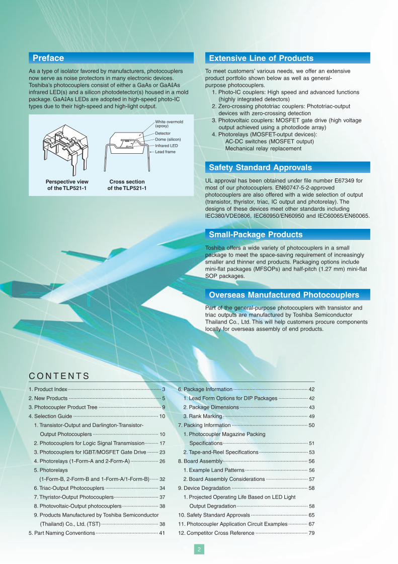
Perspective viewof the TLP521-1
Cross sectionof the TLP521-1
White overmold (epoxy)
Lead frame
Detector
Dome (silicon)
Infrared LED
To meet customers’ various needs, we offer an extensive product portfolio shown below as well as general-purpose photocouplers.
1. Photo-IC couplers: High speed and advanced functions (highly integrated detectors)
2. Zero-crossing phototriac couplers: Phototriac-output devices with zero-crossing detection
3. Photovoltaic couplers: MOSFET gate drive (high voltage output achieved using a photodiode array)
4. Photorelays (MOSFET-output devices): AC-DC switches (MOSFET output)Mechanical relay replacement
Extensive Line of Products
Safety Standard Approvals
UL approval has been obtained under file number E67349 for most of our photocouplers. EN60747-5-2-approved photocouplers are also offered with a wide selection of output (transistor, thyristor, triac, IC output and photorelay). The designs of these devices meet other standards including IEC380/VDE0806, IEC60950/EN60950 and IEC60065/EN60065.
Small-Package Products
Toshiba offers a wide variety of photocouplers in a small package to meet the space-saving requirement of increasingly smaller and thinner end products. Packaging options include mini-flat packages (MFSOPs) and half-pitch (1.27 mm) mini-flat SOP packages.
Overseas Manufactured Photocouplers
Part of the general-purpose photocouplers with transistor and triac outputs are manufactured by Toshiba Semiconductor Thailand Co., Ltd. This will help customers procure components locally for overseas assembly of end products.
PrefaceAs a type of isolator favored by manufacturers, photocouplers now serve as noise protectors in many electronic devices.Toshiba’s photocouplers consist of either a GaAs or GaA Asinfrared LED(s) and a silicon photodetector(s) housed in a mold package. GaA As LEDs are adopted in high-speed photo-IC types due to their high-speed and high-light output.
C O N T E N T S1. Product Index............................................................... 3
2. New Products .............................................................. 5
3. Photocoupler Product Tree .......................................... 9
4. Selection Guide ......................................................... 10
1. Transistor-Output and Darlington-Transistor-
Output Photocouplers ............................................... 10
2. Photocouplers for Logic Signal Transmission.......... 17
3. Photocouplers for IGBT/MOSFET Gate Drive ........ 23
4. Photorelays (1-Form-A and 2-Form-A) .................... 26
5. Photorelays
(1-Form-B, 2-Form-B and 1-Form-A/1-Form-B)...... 32
6. Triac-Output Photocouplers ...................................... 34
7. Thyristor-Output Photocouplers................................ 37
8. Photovoltaic-Output photocouplers .......................... 38
9. Products Manufactured by Toshiba Semiconductor
(Thailand) Co., Ltd. (TST) ......................................... 38
5. Part Naming Conventions.......................................... 41
6. Package Information .................................................. 42
1. Lead Form Options for DIP Packages ..................... 42
2. Package Dimensions................................................. 43
3. Rank Marking ......................................................... 49
7. Packing Information ................................................... 50
1. Photocoupler Magazine Packing
Specifications............................................................. 51
2. Tape-and-Reel Specifications................................... 53
8. Board Assembly......................................................... 56
1. Example Land Patterns.......................................... 56
2. Board Assembly Considerations .............................. 57
9. Device Degradation ................................................... 58
1. Projected Operating Life Based on LED Light
Output Degradation ................................................... 58
10. Safety Standard Approvals ...................................... 65
11. Photocoupler Application Circuit Examples ............. 67
12. Competitor Cross Reference ................................... 79
2
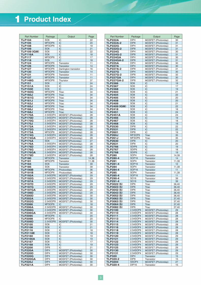
TLP104TLP105TLP108TLP109TLP109 (IGM)TLP116ATLP117TLP118TLP124TLP126TLP127TLP130TLP131TLP137TLP148GTLP151TLP151ATLP155ETLP160GTLP160JTLP161GTLP161JTLP163JTLP165JTLP166JTLP168JTLP170ATLP170DTLP170GTLP170JTLP172ATLP172GTLP173ATLP174GTLP174GATLP175ATLP176ATLP176DTLP176GTLP176GATLP179DTLP180TLP181TLP184TLP185TLP190BTLP191BTLP192ATLP192GTLP197ATLP197DTLP197GTLP197GATLP199DTLP200DTLP202ATLP202GTLP2066TLP206ATLP206GTLP206GATLP2095TLP2098TLP209DTLP2105TLP2108TLP2116TLP2118ETLP2160TLP2166ATLP2167TLP2168TLP2200TLP220ATLP220DTLP220GTLP220GATLP220JTLP221A
SO6MFSOP6MFSOP6SO6SO6SO6MFSOP6SO6MFSOP6MFSOP6MFSOP6MFSOP6MFSOP6MFSOP6MFSOP6SO6SO6SO6MFSOP6MFSOP6MFSOP6MFSOP6MFSOP6MFSOP6MFSOP6MFSOP62.54SOP42.54SOP42.54SOP42.54SOP42.54SOP42.54SOP4MFSOP62.54SOP42.54SOP4SO62.54SOP42.54SOP42.54SOP42.54SOP42.54SOP4MFSOP6MFSOP6SO6SO6MFSOP6MFSOP62.54SOP62.54SOP62.54SOP62.54SOP62.54SOP62.54SOP62.54SOP62.54SOP82.54SOP82.54SOP8MFSOP62.54SOP82.54SOP82.54SOP8MFSOP6MFSOP62.54SOP8SO8SO8SO8SO8SO8SO8SO8SO8DIP8DIP4DIP4DIP4DIP4DIP4DIP4
2220182122181718111416141111372424243434343434343434282828282828282828272828282828
14,3811,38
393936362929292929292930303018303030202030212118181919171921303030303030
ICICICICICICICICTransistorTransistorDarlington transistorTransistorTransistorTransistorThyristorICICICTriacTriacTriacTriacTriacTriacTriacTriacMOSFET (Photorelay)MOSFET (Photorelay)MOSFET (Photorelay)MOSFET (Photorelay)MOSFET (Photorelay)MOSFET (Photorelay)MOSFET (Photorelay)MOSFET (Photorelay)MOSFET (Photorelay)MOSFET(Photorelay)MOSFET (Photorelay)MOSFET (Photorelay)MOSFET (Photorelay)MOSFET (Photorelay)MOSFET (Photorelay)TransistorTransistorTransistorTransistorPhotovoltaicPhotovoltaicMOSFET (Photorelay)MOSFET (Photorelay)MOSFET (Photorelay)MOSFET (Photorelay)MOSFET (Photorelay)MOSFET (Photorelay)MOSFET (Photorelay)MOSFET (Photorelay)MOSFET (Photorelay)MOSFET (Photorelay)ICMOSFET (Photorelay)MOSFET (Photorelay)MOSFET (Photorelay)ICICMOSFET (Photorelay)ICICICICICICICICICMOSFET (Photorelay)MOSFET (Photorelay)MOSFET (Photorelay)MOSFET (Photorelay)MOSFET (Photorelay)MOSFET (Photorelay)
TLP222ATLP222A-2TLP222GTLP222G-2TLP224GTLP224G-2TLP224GATLP224GA-2TLP225ATLP227ATLP227A-2TLP227GTLP227G-2TLP227GATLP227GA-2TLP2366TLP2367TLP2368TLP2403TLP2404TLP2405TLP2408TLP2409TLP2409 (IGM)TLP2418TLP2451TLP2451ATLP2466TLP2467TLP2468TLP2530TLP2531TLP2601TLP260JTLP261JTLP2630TLP2631TLP2766TLP2767TLP2768TLP280TLP280-4TLP281TLP281-4TLP284TLP284-4TLP285TLP285-4TLP290-4TLP291-4TLP3022 (S)TLP3023 (S)TLP3042 (S)TLP3043 (S)TLP3052 (S)TLP3062 (S)TLP3063 (S)TLP3064 (S)TLP3082 (S)TLP3100TLP3110TLP3111TLP3113TLP3114TLP3115TLP3116TLP3118TLP3119TLP3120TLP3121TLP3122TLP3123TLP3125TLP3130TLP3131TLP320TLP320-2TLP3203TLP320-4
DIP4DIP8DIP4DIP8DIP4DIP8DIP4DIP8DIP4DIP4DIP8DIP4DIP8DIP4DIP8SO6SO6SO6SO8SO8SO8SO8SO8SO8SO8SO8SO8SO8SO8SO8DIP8DIP8DIP8MFSOP6MFSOP6DIP8DIP8SDIP6SDIP6SDIP6SOP4SOP16SOP4SOP16SOP4SOP16SOP4SOP16SO16SO16DIP6DIP6DIP6DIP6DIP6DIP6DIP6DIP6DIP62.54SOP62.54SOP42.54SOP42.54SOP42.54SOP42.54SOP42.54SOP42.54SOP62.54SOP42.54SOP62.54SOP42.54SOP42.54SOP42.54SOP82.54SOP42.54SOP4DIP4DIP8SSOP4DIP16
30313131303130313030313032303219171921222020212218242419181922221935352020191819
14,3914
11,3912
11,3911
11,39113939
36,4036,4036,4036,4036,4037,4037,4037,4037,40
2928282828282828282929292929292915152715
MOSFET (Photorelay)MOSFET (Photorelay)MOSFET (Photorelay)MOSFET (Photorelay)MOSFET (Photorelay)MOSFET (Photorelay)MOSFET (Photorelay)MOSFET (Photorelay)MOSFET (Photorelay)MOSFET (Photorelay)MOSFET (Photorelay)MOSFET (Photorelay)MOSFET (PhotorelayMOSFET (Photorelay)MOSFET (Photorelay)ICICICICICICICICICICICICICICICICICICTriacTriacICICICICICTransistorTransistorTransistorTransistorTransistorTransistorTransistorTransistorTransistorTransistorTriacTriacTriacTriacTriacTriacTriacTriacTriacMOSFET (Photorelay)MOSFET (Photorelay)MOSFET (Photorelay)MOSFET (Photorelay)MOSFET (Photorelay)MOSFET (Photorelay)MOSFET (Photorelay)MOSFET (Photorelay)MOSFET (Photorelay)MOSFET (Photorelay)MOSFET (Photorelay)MOSFET (Photorelay)MOSFET (Photorelay)MOSFET (Photorelay)MOSFET (Photorelay)MOSFET (Photorelay)TransistorTransistorMOSFET (Photorelay)Transistor
Part Number Package Output Part Number Package OutputPage Page
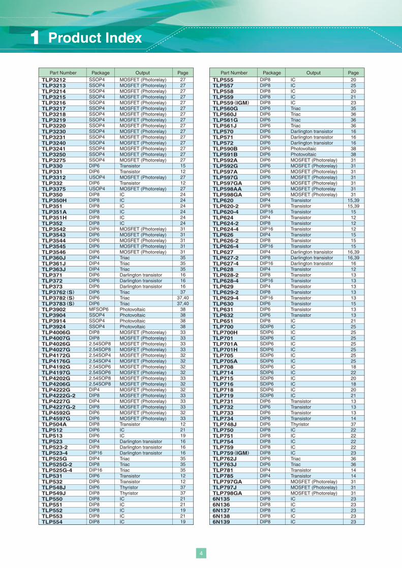
1 Product Index
3
2727272727272727272727272727271512271227242424242424313131313135353516161637
37,4037,40
3838383833333333323232323332323333333233122119161616353535121237372121192119
202520212335363636161616383831313131313131
15,3915,39
15121212151515
16,3916,39
16121313131313151313212525252525252518222018202113131314372222222223363614143131312323232323
Part Number
TLP3212TLP3213TLP3214TLP3215TLP3216TLP3217TLP3218TLP3219TLP3220TLP3230TLP3231TLP3240TLP3241TLP3250TLP3275TLP330TLP331TLP3312TLP332TLP3375TLP350TLP350HTLP351TLP351ATLP351HTLP352TLP3542TLP3543TLP3544TLP3545TLP3546TLP360JTLP361JTLP363JTLP371TLP372TLP373TLP3762 (S)TLP3782 (S)TLP3783 (S)TLP3902TLP3904TLP3914TLP3924TLP4006GTLP4007GTLP4026GTLP4027GTLP4172GTLP4176GTLP4192GTLP4197GTLP4202GTLP4206GTLP4222GTLP4222G-2TLP4227GTLP4227G-2TLP4592GTLP4597GTLP504ATLP512TLP513TLP523TLP523-2TLP523-4TLP525GTLP525G-2TLP525G-4TLP531TLP532TLP548JTLP549JTLP550TLP551TLP552TLP553TLP554
SSOP4SSOP4SSOP4SSOP4SSOP4SSOP4SSOP4SSOP4SSOP4SSOP4SSOP4SSOP4SSOP4SSOP4SSOP4DIP6DIP6USOP4DIP6USOP4DIP8DIP8DIP8DIP8DIP8DIP8DIP6DIP6DIP6DIP6DIP6DIP4DIP4DIP4DIP6DIP6DIP6DIP6DIP6DIP6MFSOP6SSOP4SSOP4SSOP4DIP8DIP82.54SOP82.54SOP82.54SOP42.54SOP42.54SOP62.54SOP62.54SOP82.54SOP8DIP4DIP8DIP4DIP8DIP6DIP6DIP8DIP6DIP6DIP4DIP8DIP16DIP4DIP8DIP16DIP6DIP6DIP6DIP8DIP8DIP8DIP8DIP8DIP8
MOSFET (Photorelay)MOSFET (Photorelay)MOSFET (Photorelay)MOSFET (Photorelay)MOSFET (Photorelay)MOSFET (Photorelay)MOSFET (Photorelay)MOSFET (Photorelay)MOSFET (Photorelay)MOSFET (Photorelay)MOSFET (Photorelay)MOSFET (Photorelay)MOSFET (Photorelay)MOSFET (Photorelay)MOSFET (Photorelay)TransistorTransistorMOSFET (Photorelay)TransistorMOSFET (Photorelay)ICICICICICICMOSFET (Photorelay)MOSFET (Photorelay)MOSFET (Photorelay)MOSFET (Photorelay)MOSFET (Photorelay)TriacTriacTriacDarlington transistorDarlington transistorDarlington transistorTriacTriacTriacPhotovoltaicPhotovoltaicPhotovoltaicPhotovoltaicMOSFET (Photorelay)MOSFET (Photorelay)MOSFET (Photorelay)MOSFET (Photorelay)MOSFET (Photorelay)MOSFET (Photorelay)MOSFET (Photorelay)MOSFET (Photorelay)MOSFET (Photorelay)MOSFET (Photorelay)MOSFET (Photorelay)MOSFET (Photorelay)MOSFET (Photorelay)MOSFET (Photorelay)MOSFET (Photorelay)MOSFET (Photorelay)TransistorICICDarlington transistorDarlington transistorDarlington transistorTriacTriacTriacTransistorTransistorThyristorThyristorICICICICIC
Package Output Part NumberPage Page
TLP555TLP557TLP558TLP559TLP559 (IGM)TLP560GTLP560JTLP561GTLP561JTLP570TLP571TLP572TLP590BTLP591BTLP592ATLP592GTLP597ATLP597GTLP597GATLP598AATLP598GATLP620TLP620-2TLP620-4TLP624TLP624-2TLP624-4TLP626TLP626-2TLP626-4TLP627TLP627-2TLP627-4TLP628TLP628-2TLP628-4TLP629TLP629-2TLP629-4TLP630TLP631TLP632TLP651TLP700TLP700HTLP701TLP701ATLP701HTLP705TLP705ATLP708TLP714TLP715TLP716TLP718TLP719TLP731TLP732TLP733TLP734TLP748JTLP750TLP751TLP754TLP759TLP759 (IGM)TLP762JTLP763JTLP781TLP785TLP797GATLP797JTLP798GA6N1356N1366N1376N1386N139
DIP8DIP8DIP8DIP8DIP8DIP6DIP6DIP6DIP6DIP6DIP6DIP6DIP6DIP6DIP6DIP6DIP6DIP6DIP6DIP6DIP6DIP4DIP8DIP16DIP4DIP8DIP16DIP4DIP8DIP16DIP4DIP8DIP16DIP4DIP8DIP16DIP4DIP8DIP16DIP6DIP6DIP6DIP8SDIP6SDIP6SDIP6SDIP6SDIP6SDIP6SDIP6SDIP6SDIP6SDIP6SDIP6SDIP6SDIP6DIP6DIP6DIP6DIP6DIP6DIP8DIP8DIP8DIP8DIP8DIP6DIP6DIP4DIP4DIP6DIP6DIP6DIP8DIP8DIP8DIP8DIP8
ICICICICICTriacTriacTriacTriacDarlington transistorDarlington transistorDarlington transistorPhotovoltaicPhotovoltaicMOSFET (Photorelay)MOSFET (Photorelay)MOSFET (Photorelay)MOSFET (Photorelay)MOSFET (Photorelay)MOSFET (PhotorelayMOSFET (Photorelay)TransistorTransistorTransistorTransistorTransistorTransistorTransistorTransistorTransistorDarlington transistorDarlington transistorDarlington transistorTransistorTransistorTransistorTransistorTransistorTransistorTransistorTransistorTransistorICICICICICICICICICICICICICICTransistorTransistorTransistorTransistorThyristorICICICICICTriacTriacTransistorTransistorMOSFET (Photorelay)MOSFET (Photorelay)MOSFET (Photorelay)ICICICICIC
Package Output
1 Product Index
4
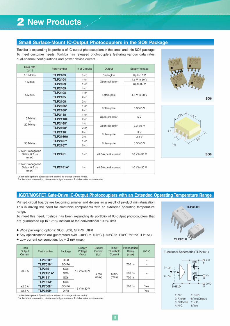
Functional Schematic (TLP2451)
2.6
6.0
3.95 5.1
1.27
2+
3–
VCC(M1)
(M2)VO
GNDSHIELD
8
6
5
Small Surface-Mount IC-Output Photocouplers in the SO8 Package
IGBT/MOSFET Gate-Drive IC-Output Photocouplers with an Extended Operating Temperature Range
1: N.C.2: Anode3: Cathode4: N.C.
5: GND6: VO (Output)7: N.C.8: VCC
TLP2403TLP2404TLP2409TLP2405TLP2408TLP2105TLP2108TLP2466*TLP2160*TLP2418TLP2118ETLP2468*TLP2168*TLP2116TLP2166ATLP2467*TLP2167*
TLP2451
TLP2451A*
0.1 Mbit/s
1 Mbit/s
5 Mbit/s
15 Mbit/s
20 Mbit/s
50 Mbit/s
Driver PropagationDelay: 0.7 μs
(max)
Driver PropagationDelay: 0.5 μs
(max)
1-ch
1-ch
1-ch
1-ch
1-ch
2-ch
2-ch
1-ch
2-ch
1-ch
2-ch
1-ch
2-ch
2-ch
2-ch
1-ch
2-ch
1-ch
1-ch
Data rate(typ.) Part Number # of Circuits
Darlington
Output
Up to 18 V
4.5 V to 30 V
Up to 30 V
Totem-pole 4.5 V to 20 V
Totem-pole 3.3 V/5 V
Open-collector
Open-collector
5 V
Open-collector 3.3 V/5 V
5 VTotem-pole
3.3 V
Totem-pole 3.3 V/5 V
±0.6-A peak current 10 V to 30 V
±0.6-A peak current 10 V to 30 V
Supply Voltage
TLP351H*TLP701H*TLP2451TLP2451A*TLP151*TLP151A*TLP700H*TLP350H*
±0.6 A 10 V to 30 V
15 V to 30 V
PeakOutputCurrent
Part NumberSupplyVoltage(VCC)
2 mA(max)
SupplyCurrent
(ICC)
DIP8
SDIP6
SO8
SO8
SO6
SO6
SDIP6
DIP8
Package
700 ns
700 ns
500 ns
±2.0 A
±2.5 A
500 ns
PropagationDelay(max)
5 mA(max)
InputThresholdCurrent
−
−
−
−
−
−
Yes
Yes
UVLO
SO8
SO8
TLP351H
TLP701H
*Under development. Specifications subject to change without notice. For the latest information, please contact your nearest Toshiba sales representative.
*Under development. Specifications subject to change without notice. For the latest information, please contact your nearest Toshiba sales representative.
Toshiba is expanding its portfolio of IC-output photocouplers in the small and thin SO8 package. To meet customer needs, Toshiba has released photocouplers featuring various data rates, dual-channel configurations and power device drivers.
Printed circuit boards are becoming smaller and denser as a result of product miniaturization. This is driving the need for electronic components with an extended operating temperature range.To meet this need, Toshiba has been expanding its portfolio of IC-output photocouplers that are guaranteed up to 125°C instead of the conventional 100°C limit.
● Wide packaging options: SO6, SO8, SDIP6, DIP8● Key specifications are guaranteed over –40°C to 125°C (–40°C to 110°C for the TLP151)● Low current consumption: ICC = 2 mA (max)
to
2 New Products
5
2.6
6.0
3.95 5.1
1.27
4.0
9.7
6.84.58
1.27
2.6
7.0
4.43.6
1: Anode 12: Cathode 13: Cathode 24: Anode 25: GND6: Output 27: Output 18: VCC
1
2
3
4
8
5
7
6
VCC
GNDSHIELD
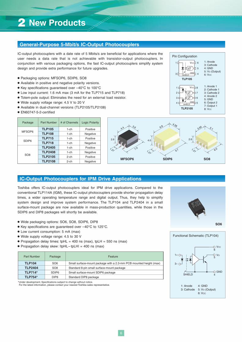
TLP2105
TLP105
1: Anode3: Cathode4: GND5: VO (Output)6: VCC
1
3
6
4
5
VCC
GNDSHIELD
1+
3–
VCC
VO
GND
6
5
4SHIELD
Functional Schematic (TLP104)
1.27
General-Purpose 5-Mbit/s IC-Output Photocouplers
IC-output photocouplers with a date rate of 5 Mbits/s are beneficial for applications where the user needs a data rate that is not achievable with transistor-output photocouplers. In conjunction with various packaging options, the fast IC-output photocouplers simplify system design and provide extra performance for future upgrades.
● Packaging options: MFSOP6, SDIP6, SO8● Available in positive and negative polarity versions.● Key specifications guaranteed over –40°C to 100°C● Low input current: 1.6 mA max (3 mA for the TLP715 and TLP718)● Totem-pole output: Eliminates the need for an external load resistor.● Wide supply voltage range: 4.5 V to 20 V● Available in dual-channel versions (TLP2105/TLP2108)● EN60747-5-2-certified
IC-Output Photocouplers for IPM Drive Applications
Toshiba offers IC-output photocouplers ideal for IPM drive applications. Compared to the conventional TLP114A (IGM), these IC-output photocouplers provide shorter propagation delay times, a wider operating temperature range and digital output. Thus, they help to simplify system design and improve system performance. The TLP104 and TLP2404 in a small surface-mount package are now available in mass-production quantities, while those in the SDIP6 and DIP8 packages will shortly be available.
● Wide packaging options: SO6, SO8, SDIP6, DIP8● Key specifications are guaranteed over –40°C to 125°C.● Low current consumption: 5 mA (max)● Wide supply voltage range: 4.5 to 30 V● Propagation delay times: tpHL = 400 ns (max), tpLH = 550 ns (max)● Propagation delay skew: |tpHL– tpLH| = 400 ns (max)
MFSOP6
SDIP6
SO8
TLP105TLP108TLP715TLP718TLP2405TLP2408TLP2105TLP2108
1-ch
1-ch
1-ch
1-ch
1-ch
1-ch
2-ch
2-ch
Positive
Negative
Positive
Negative
Positive
Negative
Positive
Negative
Package Part Number # of Channels Logic Polarity
TLP104TLP2404TLP714*TLP754*
SO6
SO8
SDIP6
DIP8
Small surface-mount package with a 2.3-mm PCB mounted height (max)
Standard 8-pin small surface-mount package
Small surface-mount SDIP6 package
Standard DIP8 package
Part Number Package Feature
SO8
SO6
SDIP6MFSOP6
Pin Configuration
*Under development. Specifications subject to change without notice. For the latest information, please contact your nearest Toshiba sales representative. 1: Anode
3: Cathode4: GND5: VO (Output)6: VCC
2 New Products
6
1.65
3.25
2.852.2
1.27
1 4
2 3
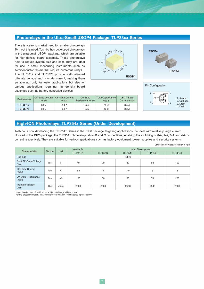
Photorelays in the Ultra-Small USOP4 Package: TLP33xx Series
There is a strong market need for smaller photorelays. To meet this need, Toshiba has developed photorelays in the ultra-small USOP4 package, which are suitable for high-density board assembly. These photorelays help to reduce system size and cost. They are ideal for use in small measuring instruments such as semiconductor testers that require numerous relays.The TLP3312 and TLP3375 provide well-balanced off-state voltage and on-state current, making them suitable not only for tester applications but also for various applications requiring high-density board assembly such as battery-controlled devices.
TLP3312TLP3375
60 V
50 V
0.4 A
0.3 A
1.5 Ω
1.5 Ω
20 pF
12 pF
Part NumberOff-State Voltage
(max)On-State Current
(max)On-State
Resistance (max)Total Capacitance
(typ.)
3 mA
3 mA
LED TriggerCurrent (max)
Pin Configuration
1. Anode2. Cathode3. Drain4. Drain
USOP4
USOP4
SSOP4
High-ION Photorelays: TLP354x Series (Under Development)
Package
VOFF
ION
RON
BVS
V
A
mΩ
Vrms
40
2.5
100
2500
20
4
50
2500
40
3.5
60
2500
60
3
70
2500
100
2
200
2500
DIP6
Characteristic Symbol UnitAvailable Under Development
Toshiba is now developing the TLP354x Series in the DIP6 package targeting applications that deal with relatively large current.Housed in the DIP6 package, the TLP354x photorelays allow B and C connections, enabling the switching of 8-A, 7-A, 6-A and 4-A dc current respectively. They are suitable for various applications such as factory equipment, power supplies and security systems.
Peak Off-State Voltage (min)
On-State Current (max)
On-State Resistance (max)
Isolation Voltage (min)
TLP3542 TLP3543 TLP3544 TLP3545 TLP3546
− −
Scheduled for mass production in April
*Under development. Specifications subject to change without notice. For the latest information, please contact your nearest Toshiba sales representative.
7
2.3
7.0
4.553.7
1.27
TLP104TLP109TLP116ATLP2366*TLP118TLP2368*TLP2367*
1 Mbit/s Open-collector, optimized for IPM drive
Open-collector
Totem-pole inverting logic
Open-collector inverting logic
Totem-pole inverting logic
1 Mbit/s
20 Mbit/s
50 Mbit/s
20 Mbit/s
4.5 V to 30 V
4.5 V to 30 V
5 V
3.3 V/5 V
5 V
3.3 V/5 V
3.3 V/5 V
Part NumberData rate
(typ.)Output Supply voltage
5 mA
−
5 mA
5 mA
5 mA
5 mA
5 mA
Input ThresholdCurrent (max)
SO6
SO6
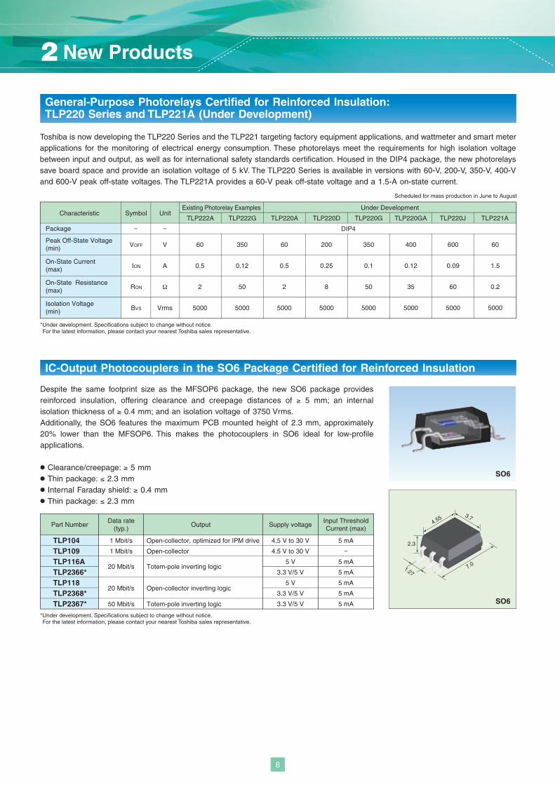
IC-Output Photocouplers in the SO6 Package Certified for Reinforced Insulation
Despite the same footprint size as the MFSOP6 package, the new SO6 package provides reinforced insulation, offering clearance and creepage distances of ≥ 5 mm; an internal isolation thickness of ≥ 0.4 mm; and an isolation voltage of 3750 Vrms.Additionally, the SO6 features the maximum PCB mounted height of 2.3 mm, approximately 20% lower than the MFSOP6. This makes the photocouplers in SO6 ideal for low-profile applications.
● Clearance/creepage: ≥ 5 mm● Thin package: ≤ 2.3 mm● Internal Faraday shield: ≥ 0.4 mm● Thin package: ≤ 2.3 mm
*Under development. Specifications subject to change without notice. For the latest information, please contact your nearest Toshiba sales representative.
*Under development. Specifications subject to change without notice. For the latest information, please contact your nearest Toshiba sales representative.
General-Purpose Photorelays Certified for Reinforced Insulation: TLP220 Series and TLP221A (Under Development)
Toshiba is now developing the TLP220 Series and the TLP221 targeting factory equipment applications, and wattmeter and smart meter applications for the monitoring of electrical energy consumption. These photorelays meet the requirements for high isolation voltage between input and output, as well as for international safety standards certification. Housed in the DIP4 package, the new photorelays save board space and provide an isolation voltage of 5 kV. The TLP220 Series is available in versions with 60-V, 200-V, 350-V, 400-V and 600-V peak off-state voltages. The TLP221A provides a 60-V peak off-state voltage and a 1.5-A on-state current.
Package
VOFF
ION
RON
BVS
V
A
Ω
Vrms
60
0.5
2
5000
350
0.12
50
5000
60
0.5
2
5000
200
0.25
8
5000
350
0.1
50
5000
400
0.12
35
5000
600
0.09
60
5000
60
1.5
0.2
5000
DIP4
Characteristic Symbol UnitExisting Photorelay Examples Under Development
Peak Off-State Voltage (min)
On-State Current (max)
On-State Resistance (max)
Isolation Voltage (min)
TLP222A TLP222G TLP220A TLP220D TLP220G TLP220GA TLP221ATLP220J
− −
Scheduled for mass production in June to August
2 New Products
8
VCC
GND
Vcc
GND
ZC
Photocoupler Product Tree
DIP4
DIP4
SDIP6
SDIP6
SO6
SO6
SO8
DIP8
DIP8
DIP16
DIP16DIP6
DIP6
SOP16
SO16
SOP16
2.54SOP8
2.54SOP82.54SOP6
2.54SOP6
2.54SOP4
2.54SOP4
SSOP4
USOP4
SSOP4
MFSOP6
MFSOP6
SOP4
SOP4
● General-purpose packages● Lead-forming options for surface mounting
Package
Transistor-Output
Transistor-Output IC-Output
Photorelays
Thyristor- and Triac-Output Photovoltaic-Output
Triac Output Thyristor Output Photovoltaic-Output
Darlington-Transistor Output Logic Output
Gate Drive
Photorelays
● ≥ 7-mm clearance/creepage; ≥ 0.4-mm isolation thickness● 6-pin SMD package (1.27-mm lead pitch)
● ≥ 5-mm clearance/creepage; ≥ 0.4-mm isolation thickness● 5-pin SMD package (1.27-mm lead pitch); low-profile
● SMD package (1.27-mm lead pitch)
● SMD package (2.54-mm lead pitch)
● Ultra-small; SMD package (1.27-mm lead pitch)
USOP4 ● Ultra-small; SMD package (1.27-mm lead pitch)
● 4-pin SMD package (1.27-mm lead pitch)● 16-pin SMD package (1.27-mm lead pitch)
SO16
SO8 ● 8-pin SMD package (1.27-mm lead pitch)● 16-pin SMD package (1.27-mm lead pitch)
Output Choices
3 Photocoupler Product Tree
9
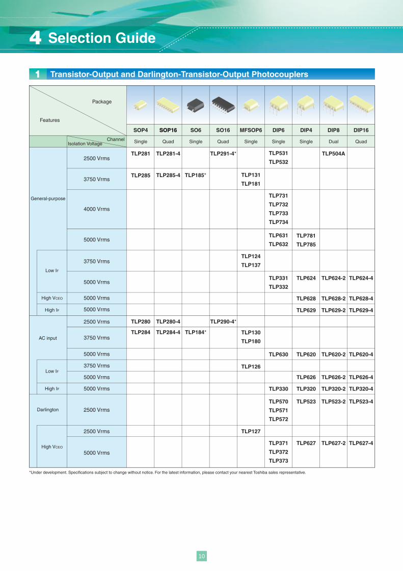
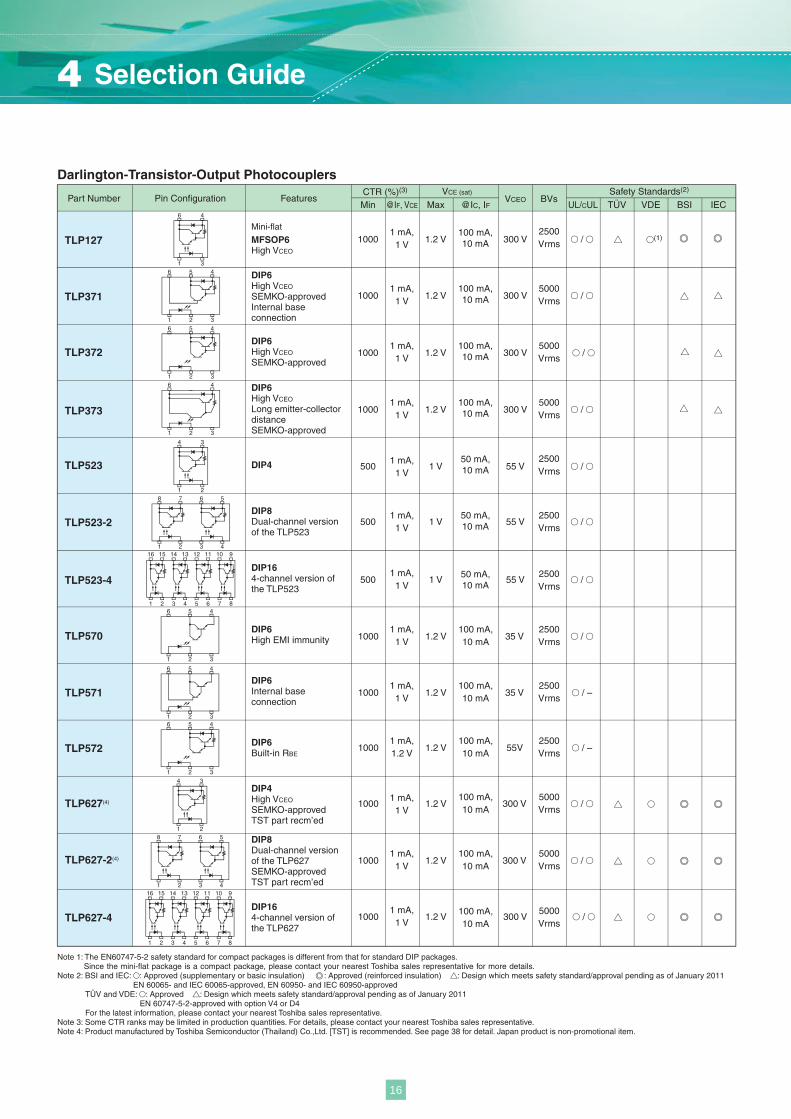
Transistor-Output and Darlington-Transistor-Output Photocouplers1
Isolation VoltageChannel Single Quad Single Single Single Dual Quad
SOP4 SOP16SOP16
Quad
SO16 MFSOP6
Single
SO6 DIP4DIP6 DIP8 DIP16
5000 Vrms
5000 Vrms
5000 Vrms
5000 Vrms
5000 Vrms
5000 Vrms
5000 Vrms
5000 Vrms
4000 Vrms
3750 Vrms
3750 Vrms
3750 Vrms
3750 Vrms
2500 Vrms
2500 Vrms
2500 Vrms
2500 Vrms
TLP280 TLP280-4
TLP284 TLP284-4 TLP184*
TLP290-4*
TLP285
TLP124
TLP137
TLP131
TLP181
TLP126
TLP130
TLP180
TLP127
TLP731
TLP732
TLP733
TLP734
TLP331
TLP332
TLP631
TLP632
TLP624
TLP781
TLP785
TLP624-2 TLP624-4
TLP330 TLP320 TLP320-2
TLP281 TLP281-4
TLP285-4 TLP185*
TLP291-4* TLP531
TLP532
TLP504A
TLP630
TLP626 TLP626-2 TLP626-4
TLP620 TLP620-2 TLP620-4
TLP320-4
TLP570
TLP571
TLP572
TLP523 TLP523-2 TLP523-4
TLP371
TLP372
TLP373
TLP627 TLP627-2 TLP627-4
TLP628 TLP628-2 TLP628-4
TLP629 TLP629-2 TLP629-4
High VCEO
General-purpose
High IF
High IF
Low IF
AC input
Low IF
Darlington
High VCEO
Package
Features
*Under development. Specifications subject to change without notice. For the latest information, please contact your nearest Toshiba sales representative.
4 Selection Guide
10
4
1
3
2
16
1
15
2
14
3
13
4
12
5
11
6
10
7
9
8
4
1
3
2
4
1
3
2
16
1
15
2
14
3
13
4
12
5
11
6
10
7
9
8
1
6 4
3
6
1
5 4
3
6
1
5 4
3
6
1
4
3
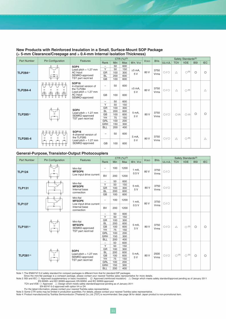
New Products with Reinforced Insulation in a Small, Surface-Mount SOP Package (≥ 5-mm Clearance/Creepage and ≥ 0.4-mm Internal Isolation Thickness)
Part Number Pin Configuration Features VCEO BVsRank Min Max VDE BSI IEC
Safety Standards(2)
TÜVCTR (%)(3)
@IF, VCE UL/CUL
Note 1: The EN60747-5-2 safety standard for compact packages is different from that for standard DIP packages.Since the mini-flat package is a compact package, please contact your nearest Toshiba sales representative for more details.
Note 2: BSI and IEC: : Approved (supplementary or basic insulation) : Approved (reinforced insulation) : Design which meets safety standard/approval pending as of January 2011EN 60065- and IEC 60065-approved, EN 60950- and IEC 60950-approved
TÜV and VDE: : Approved : Design which meets safety standard/approval pending as of January 2011EN 60747-5-2-approved with option V4 or D4
For the latest information, please contact your nearest Toshiba sales representative.Note 3: Some CTR ranks may be limited in production quantities. For details, please contact your nearest Toshiba sales representative.Note 4: Product manufactured by Toshiba Semiconductor (Thailand) Co.,Ltd. [TST] is recommended. See page 38 for detail. Japan product is non-promotional item.
±5 mA,5 V
GB 100
TLP284-4
– 50 600
600
SOP164-channel version of the TLP284Lead pitch = 1.27 mmAC InputSEMKO-approved
3750Vrms
80 V / (1)
– 50 600Y 50 150
GR 100 300BL 200GB 100
600600
TLP284(4)
SOP4Lead pitch = 1.27 mmAC InputSEMKO-approvedTST part recm’ed
±5 mA,5 V
3750Vrms
80 V / (1)
TLP285(4)
SOP4Lead pitch = 1.27 mmSEMKO-approvedTST part recm’ed
– 50 600Y 50 150
GR 100 300BL 200GB 100YH 75 150
GRL 100 200GRH 150 300BLL 200 400
600600
5 mA,5 V
3750Vrms
80 V / (1)(1)
5 mA, 5 V
GB 100
TLP285-4
– 50 600
600
SOP164-channel version of the TLP285Lead pitch = 1.27 mmSEMKO-approved
3750Vrms
80 V / (1)
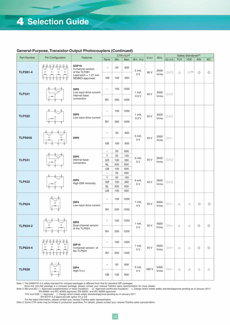
General-Purpose, Transistor-Output Photocouplers
Part Number Pin Configuration Features VCEO BVsRank Min Max VDE BSI IEC
Safety Standards(2)
TÜVCTR (%)(3)
@IF, VCE UL/CUL
Mini-flatMFSOP6Low input drive current
1 mA,0.5 V
BV 200TLP124
– 100 1200
1200
3750Vrms
80 V /
– 50 600Y 50 150 5 mA,
5 VGR 100 300BL 200GB 100
TLP131600600
Mini-flatMFSOP6Internal base connection
3750Vrms
80 V /
Mini-flatMFSOP6Low input drive currentInternal base connection
BV 200TLP137
– 1003750Vrms
1 mA,0.5 V
1200
1200
80 V /
– 50 600Y 50 150
GR 100 300BL 200GB 100YH 75 150
GRL 100 200GRH 150 300BLL 200 400
600600TLP181(4)
Mini-flatMFSOP6SEMKO-approvedTST part recm’ed
5 mA,5 V
3750Vrms
80 V / (1)
TLP281(4)
SOP4Lead pitch = 1.27 mmSEMKO-approvedTST part recm’ed
– 50 600Y 50 150
GR 100 300BL 200GB 100YH 75 150
GRL 100 200GRH 150 300BLL 200 400
600600
5 mA,5 V
2500Vrms
80 V / (1)(1)
11
16
1
15
2
14
3
13
4
12
5
11
6
10
7
9
8
8
1
6 5
43
7
2
6
1
5 4
32
6
1
5 4
32
6
1
5 4
32
6
1
5 4
32
4
1
3
2
8
1
6 5
43
7
2
16
1
15
2
14
3
13
4
12
5
11
6
10
7
9
8
4
1
3
2
Note 1: The EN60747-5-2 safety standard for compact packages is different from that for standard DIP packages.Since the mini-flat package is a compact package, please contact your nearest Toshiba sales representative for more details.
Note 2: BSI and IEC: : Approved (supplementary or basic insulation) : Approved (reinforced insulation) : Design which meets safety standard/approval pending as of January 2011EN 60065- and IEC 60065-approved, EN 60950- and IEC 60950-approved
TÜV and VDE: : Approved : Design which meets safety standard/approval pending as of January 2011EN 60747-5-2-approved with option V4 or D4
For the latest information, please contact your nearest Toshiba sales representative.Note 3: Some CTR ranks may be limited in production quantities. For details, please contact your nearest Toshiba sales representative.
General-Purpose, Transistor-Output Photocouplers (Continued)
Part Number Pin Configuration Features VCEO BVsRank Min Max VDE BSI IEC
Safety Standards(2)
TÜVCTR (%)(3)
@IF, VCE UL/CUL
5 mA,5 V
GB 100
TLP281-4
– 50 600
600
SOP164-channel version of the TLP281Lead pitch = 1.27 mmSEMKO-approved
2500Vrms
80 V / (1)
– 50
GB 100
TLP504A DIP85 mA,
5 V2500Vrms
600
600
55 V / –
DIP6Low input drive currentInternal base connection
DIP6Low input drive current
BV 200
BV 200
TLP332
– 100
TLP331
– 1001 mA,0.5 V
5000Vrms
1200
1200
55 V /
1 mA,0.5 V
5000Vrms
1200
1200
55 V /
TLP531
50 600
Y 50 150
GR 100 300
BL 200
GB 100
600
DIP6Internal base connection
5 mA,5 V
2500Vrms
55 V /
5 mA,5 V
2500Vrms
55 V /TLP532
50 600
Y 50 150
GR 100 300
BL 200
GB 100
600
DIP6High EMI immunity
–
–
600
600
TLP624DIP4Low input drive current
1 mA,5 V
BV 200
– 100 1200
1200
5000Vrms
55 V / −
BV 200
TLP624-2
– 100 1200DIP8Dual-channel version of the TLP624
1 mA,5 V
5000Vrms
55 V / –
1200
BV 200
TLP624-4
– 100DIP164-channel version of the TLP624
1 mA,5 V
5000Vrms
1200
55 V / –
DIP4High VCEO
GB 100
TLP628
– 505 mA,
5 V5000Vrms
600
350 V / –
1200
600
4 Selection Guide
12
4
1
3
2
8
1
6 5
43
7
2
16
1
15
2
14
3
13
4
12
5
11
6
10
7
9
8
6
1
5 4
32
8
1
6 5
43
7
2
16
1
15
2
14
3
13
4
12
5
11
6
10
7
9
8
6
1
5 4
32
6
1
5 4
32
6
1
5 4
32
6
1
5 4
32
DIP4High input currentIF = 150 mA
TLP629100 mA,
1 V5000Vrms
– 20 80 55 V / –
80TLP629-2 – 20DIP8Dual-channel version of the TLP629
100 mA,1 V
5000Vrms
55 V / –
TLP629-4DIP164-channel version of the TLP629
100 mA,1 V
5000Vrms
– 20 80 55 V / –
– 50 600
600
GR 100 300
GB 100TLP631DIP6Internal base connection
5 mA,5 V
5000Vrms
55 V /
Note 1: The EN60747-5-2 safety standard for compact packages is different from that for standard DIP packages.Since the mini-flat package is a compact package, please contact your nearest Toshiba sales representative for more details.
Note 2: BSI and IEC: : Approved (supplementary or basic insulation) : Approved (reinforced insulation) : Design which meets safety standard/approval pending as of January 2011EN 60065- and IEC 60065-approved, EN 60950- and IEC 60950-approved
TÜV and VDE: : Approved : Design which meets safety standard/approval pending as of January 2011EN 60747-5-2-approved with option V4 or D4
For the latest information, please contact your nearest Toshiba sales representative.Note 3: Some CTR ranks may be limited in production quantities. For details, please contact your nearest Toshiba sales representative.
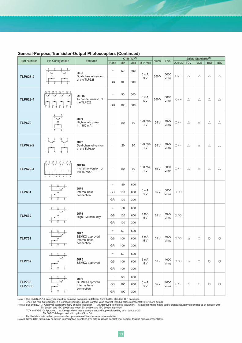
General-Purpose, Transistor-Output Photocouplers (Continued)
Part Number Pin Configuration Features VCEO BVsRank Min Max VDE BSI IEC
Safety Standards(2)
TÜVCTR (%)(3)
@IF, VCE UL/CUL
GB 100
600
TLP628-2
– 50DIP8Dual-channel version of the TLP628
5 mA,5 V
5000Vrms
350 V / –
GB 100
TLP628-4
– 50DIP164-channel version of the TLP628
5 mA,5 V
600
600
600
350 V5000Vrms / –
– 50 600
GR 100 300
TLP632DIP6High EMI immunity
5 mA,5 V
5000Vrms
55 V /GB 100
5 mA,5 V
4000Vrms
55 V /
– 50 600
GB 100TLP731
GR 100 300
DIP6SEMKO-approvedInternal base connection
600
600
TLP732
– 50 600
GR 100 300
GB 100DIP6SEMKO-approved
5 mA,5 V
4000Vrms
55 V /
5 mA,5 V
4000Vrms
55 V / –
– 50 600
GB 100
600
600TLP733TLP733F
GR 100 300
DIP6SEMKO-approvedInternal base connection
13
6
1
5 4
32
4
1
3
2
6
1
4
3
16
1
15
2
14
3
13
4
12
5
11
6
10
7
9
8
6
1
4
3
4
1
3
2
6
1
5 4
3
4
1
3
2
*Under development. Specifications subject to change without notice. For the latest information, please contact your nearest Toshiba sales representative.Note 1: The EN60747-5-2 safety standard for compact packages is different from that for standard DIP packages.
Since the mini-flat package is a compact package, please contact your nearest Toshiba sales representative for more details.Note 2: BSI and IEC: : Approved (supplementary or basic insulation) : Approved (reinforced insulation) : Design which meets safety standard/approval pending as of January 2011
EN 60065- and IEC 60065-approved, EN 60950- and IEC 60950-approvedTÜV and VDE: : Approved : Design which meets safety standard/approval pending as of January 2011
EN 60747-5-2-approved with option V4 or D4For the latest information, please contact your nearest Toshiba sales representative.
Note 3: Some CTR ranks may be limited in production quantities. For details, please contact your nearest Toshiba sales representative.Note 4: Product manufactured by Toshiba Semiconductor (Thailand) Co.,Ltd. [TST] is recommended. See page 38 for detail. Japan product is non-promotional item.Note 5: For safety standard compliance criteria including the operating temperature conditions, please contact your nearest Toshiba representative.Note 6: About the package dimensions and lead form options, see each datasheet.
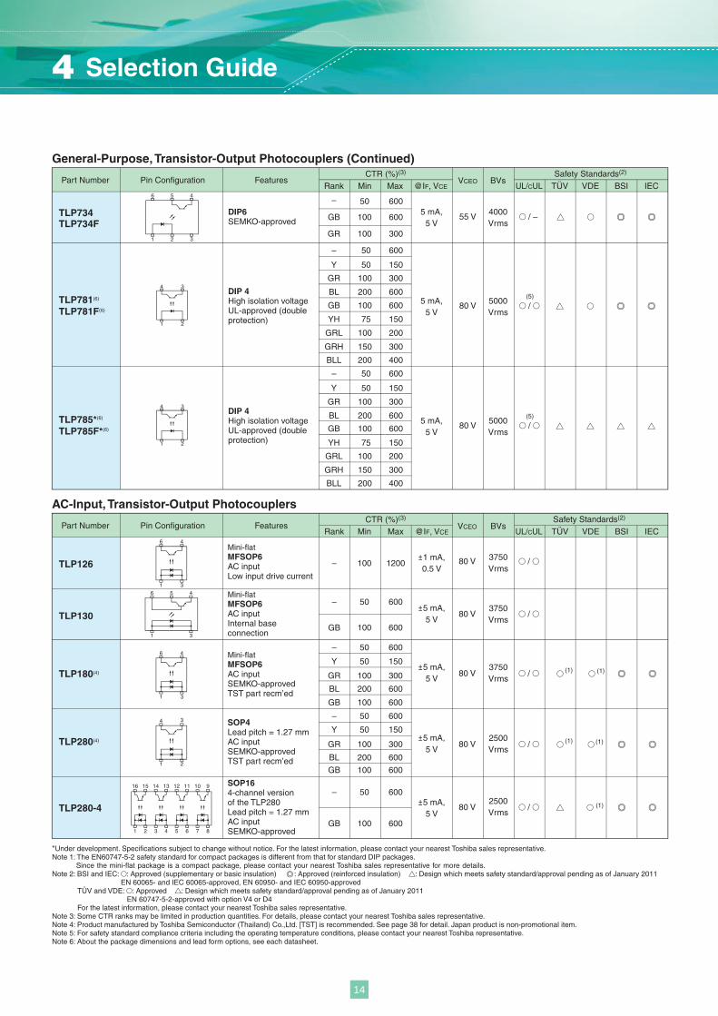
General-Purpose, Transistor-Output Photocouplers (Continued)
Part Number Pin Configuration Features VCEO BVsRank Min Max VDE BSI IEC
Safety Standards(2)
TÜVCTR (%)(3)
@IF, VCE UL/CUL
5 mA,5 V
4000Vrms
55 V / –
– 50 600
600TLP734TLP734F
GR 100 300
GB 100DIP6SEMKO-approved
TLP781(6)
TLP781F(6)
DIP 4High isolation voltageUL-approved (double protection)
/5 mA,
5 V5000Vrms
80 V
– 50 600
Y 50 150
GR 100 300
BL 200
GB 100
YH 75 150
GRL 100 200
GRH 150 300
BLL 200 400
600
600
AC-Input, Transistor-Output Photocouplers
Part Number Pin Configuration Features VCEO BVsRank Min Max VDE BSI IEC
Safety Standards(2)
TÜVCTR (%)(3)
@IF, VCE UL/CUL
Mini-flatMFSOP6AC inputLow input drive current
±1 mA,0.5 V
1200TLP126 – 1003750Vrms
80 V /
±5 mA,5 V
GB 100
TLP280-4
– 50 600
600
SOP164-channel version of the TLP280Lead pitch = 1.27 mmAC inputSEMKO-approved
2500Vrms
80 V / (1)
– 50 600
Y 50 150
GR 100 300
BL 200
GB 100
– 50 600
Y 50 150
GR 100 300
BL 200
GB 100
600
600
TLP280(4)
600
600
TLP180(4)
Mini-flatMFSOP6AC inputSEMKO-approvedTST part recm’ed
SOP4Lead pitch = 1.27 mmAC inputSEMKO-approvedTST part recm’ed
/
±5 mA,5 V
2500Vrms
80 V /
±5 mA,5 V
3750Vrms
80 V (1) (1)
(1) (1)
– 50±5 mA,
5 VGB 100
TLP130
600
600
Mini-flatMFSOP6AC inputInternal base connection
3750Vrms
80 V /
(5)
TLP785*(6)
TLP785F*(6)
DIP 4High isolation voltageUL-approved (double protection)
/5 mA,
5 V5000Vrms
80 V
– 50 600
Y 50 150
GR 100 300
BL 200
GB 100
YH 75 150
GRL 100 200
GRH 150 300
BLL 200 400
600
600
(5)
4 Selection Guide
14
4
1
3
2
8
1
6 5
43
7
2
16
1
15
2
14
3
13
4
12
5
11
6
10
7
9
8
6
1 2
5 4
3
4
1
3
2
6
1
5 4
32
8
1
6 5
43
7
216
1
15
2
14
3
13
4
12
5
11
6
10
7
9
8
4
1
3
2
8
1
6 5
43
7
2
16
1
15
2
14
3
13
4
12
5
11
6
10
7
9
8
VCEO BVsRank Max VDE BSI IECTÜV@IF, VCEMin UL/CUL
DIP4Low input drive currentAC input
±1 mA,0.5 V
BV 200
1200TLP626– 100
5000Vrms
55 V / −
BV 200
TLP626-2
– 100DIP8Dual-channel version of the TLP626
±1 mA,0.5 V
5000Vrms1200 55 V / –
BV 200
TLP626-4
TLP630
– 100DIP164-channel version of the TLP626
±1 mA,0.5 V
5000Vrms1200 55 V / –
– 50
GB 100
600
DIP6AC inputHigh isolation voltageInternal base connection
±5 mA,5 V
5000Vrms55 V /
Note 1: The EN60747-5-2 safety standard for compact packages is different from that for standard DIP packages.Since the mini-flat package is a compact package, please contact your nearest Toshiba sales representative for more details.
Note 2: BSI and IEC: : Approved (supplementary or basic insulation) : Approved (reinforced insulation) : Design which meets safety standard/approval pending as of January 2011EN 60065- and IEC 60065-approved, EN 60950- and IEC 60950-approved
TÜV and VDE: : Approved : Design which meets safety standard/approval pending as of January 2011EN 60747-5-2-approved with option V4 or D4
For the latest information, please contact your nearest Toshiba sales representative.Note 3: Some CTR ranks may be limited in production quantities. For details, please contact your nearest Toshiba sales representative.Note 4: Product manufactured by Toshiba Semiconductor (Thailand) Co.,Ltd. [TST] is recommended. See page 38 for detail. Japan product is non-promotional item.
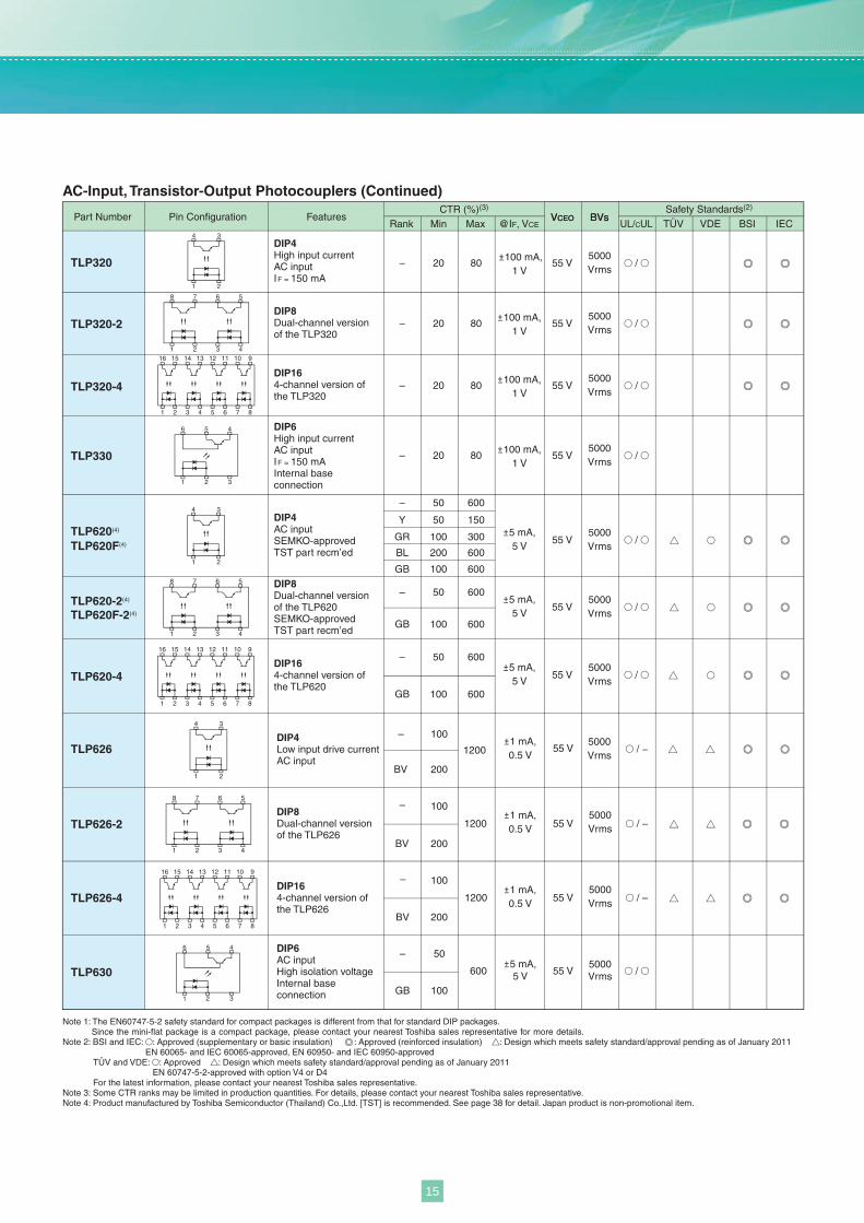
AC-Input, Transistor-Output Photocouplers (Continued)
Part Number Pin Configuration Features VCEO BVsSafety Standards(2)CTR (%)(3)
DIP4High input currentAC inputIF = 150 mA
TLP320 ±100 mA,1 V
5000Vrms
– 20 80 55 V /
DIP6High input currentAC inputIF = 150 mAInternal base connection
TLP3305000Vrms
±100 mA,1 V
– 20 80 55 V /
TLP320-2DIP8Dual-channel version of the TLP320
– 20±100 mA,
1 V
5000Vrms
80 55 V /
TLP320-4DIP164-channel version of the TLP320
±100 mA,1 V
5000Vrms
– 20 80 55 V /
– 50 600
TLP620(4)
TLP620F(4)
Y 50 150
BL 200
GB 100
GR 100 300
600
600
DIP4AC inputSEMKO-approvedTST part recm’ed
±5 mA,5 V
5000Vrms
55 V /
GB 100
TLP620-2(4)
TLP620F-2(4)
– 50DIP8Dual-channel version of the TLP620SEMKO-approvedTST part recm’ed
±5 mA,5 V
5000Vrms
600
600
55 V /
GB 100
TLP620-4
– 50DIP164-channel version of the TLP620
±5 mA,5 V
5000Vrms
600
600
55 V /
15
6
1
4
36
1
5 4
326
1
5 4
326
1
4
32
4
1
3
28
1
6 5
43
7
216
1
15
2
14
3
13
4
12
5
11
6
10
7
9
8
6
1
5 4
32
6
1
5 4
32
6
1
5 4
32
4
1
3
28
1
6 5
43
7
216
1
15
2
14
3
13
4
12
5
11
6
10
7
9
8
Note 1: The EN60747-5-2 safety standard for compact packages is different from that for standard DIP packages.Since the mini-flat package is a compact package, please contact your nearest Toshiba sales representative for more details.
Note 2: BSI and IEC: : Approved (supplementary or basic insulation) : Approved (reinforced insulation) : Design which meets safety standard/approval pending as of January 2011EN 60065- and IEC 60065-approved, EN 60950- and IEC 60950-approved
TÜV and VDE: : Approved : Design which meets safety standard/approval pending as of January 2011EN 60747-5-2-approved with option V4 or D4
For the latest information, please contact your nearest Toshiba sales representative.Note 3: Some CTR ranks may be limited in production quantities. For details, please contact your nearest Toshiba sales representative.Note 4: Product manufactured by Toshiba Semiconductor (Thailand) Co.,Ltd. [TST] is recommended. See page 38 for detail. Japan product is non-promotional item.
Darlington-Transistor-Output Photocouplers
Part Number Pin Configuration Features VCEO BVsMin Max VDE BSI IEC
Safety Standards(2)
TÜVCTR (%)(3)
@IC, IF@IF, VCE
VCE (sat)
UL/CUL
TLP127Mini-flat
MFSOP6High VCEO
1 mA,1 V
100 mA,10 mA
2500Vrms1.2 V 300 V1000 / (1)
TLP372
TLP371
DIP6High VCEO
SEMKO-approvedInternal base connection
DIP6High VCEO
SEMKO-approved
TLP373
DIP6High VCEO
Long emitter-collector distanceSEMKO-approved
/1 mA,
1 V100 mA,10 mA
5000Vrms
1000 1.2 V 300 V
/1 mA,
1 V100 mA,10 mA
5000Vrms
1000 1.2 V 300 V
/1 mA,
1 V100 mA,10 mA
5000Vrms
1000 1.2 V 300 V
TLP52350 mA,10 mA
2500Vrms1 V 55 V /500DIP4 1 mA,
1 V
TLP523-21 mA,
1 V50 mA,10 mA
2500Vrms
500 1 V 55 V /DIP8Dual-channel version of the TLP523
DIP164-channel version of the TLP523
TLP523-450 mA,10 mA
1 mA,1 V
2500Vrms
500 1 V 55 V /
TLP5701 mA,
1 V100 mA,10 mA
2500Vrms
1000 1.2 V 35 V /
1 mA,1 V
100 mA,10 mA
2500Vrms
1000 1.2 V 35 V / –
DIP6High EMI immunity
TLP572 / –1 mA,1.2 V
100 mA,10 mA
2500Vrms
1000 1.2 V 55V
TLP571DIP6Internal base connection
DIP6Built-in RBE
TLP627(4)
DIP4High VCEO
SEMKO-approvedTST part recm’ed
100 mA,10 mA
5000Vrms
1.2 V 300 V10001 mA,
1 V/
TLP627-2(4)
DIP8Dual-channel version of the TLP627SEMKO-approvedTST part recm’ed
1 mA,1 V
100 mA,10 mA
5000Vrms
1000 1.2 V 300 V /
DIP164-channel version of the TLP627
TLP627-4100 mA,10 mA
1 mA,1 V
5000Vrms
1000 1.2 V 300 V /
4 Selection Guide
16
SH
IELD
6
1
5 4
3
Vcc
GN
D
VC
C
GN
D
8
1
6 5
43
7
2
SH
IELD
SH
IELD
6
1
5 4
3
Vcc
GN
D
1 Mbit/s
IPMdrive
Dualpolarityinput5 Mbit/s
5 V
5 V
3.3 V3.3 V/5 V
3.3 V/5 V
3.3 V/5 V
5 V
10 Mbit/s
15 to 20 Mbit/s
50 Mbit/s
0.3 Mbit/s
(TLP112)*2 TLP109 TLP719 TLP512
TLP2403
TLP2409
TLP553
TLP550 TLP2530
6N1386N1396N135
(TLP112A)*2 TLP551 TLP2531 6N136(TLP114A)*2 TLP559
TLP651TLP750TLP751TLP759
(TLP114A(IGM))*3 TLP559(IGM)TLP2409(IGM)TLP759(IGM)
TLP109(IGM)
TLP105 TLP715TLP2405TLP108 TLP718TLP2408
TLP2105TLP2108
TLP2095TLP2098
TLP104TLP714*1
TLP2404TLP754*1
TLP555TLP558TLP2200
(TLP113)*4 TLP513 TLP552 TLP2630 6N137(TLP115)*4 TLP554 TLP2631(TLP115A)*4 TLP2601
TLP2366*1
TLP116A
TLP2368*1
TLP118
TLP2367*1 TLP2467*1
TLP2466*1 TLP2160*1
TLP2168*1
TLP2116
TLP2118
TLP2166ATLP2766*1
TLP708
TLP716
TLP2768*1
TLP2767*1TLP2167*1
TLP2468*1
TLP2418
TLP117
TLP2066
(TLP116)*5
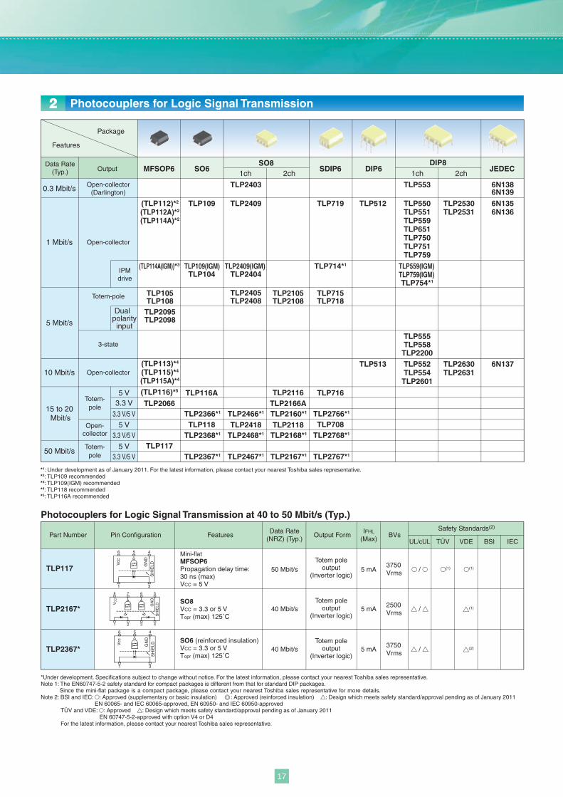
SDIP6 DIP6 JEDEC1ch 2ch 1ch 2ch
MFSOP6 SO6SO8 DIP8Data Rate
(Typ.) Output
Open-collector(Darlington)
Open-collector
Open-collector
Open-collector
Totem-pole
Totem-pole
Totem-pole
3-state
Package
Features
*1: Under development as of January 2011. For the latest information, please contact your nearest Toshiba sales representative.*2: TLP109 recommended*3: TLP109(IGM) recommended*4: TLP118 recommended*5: TLP116A recommended
Photocouplers for Logic Signal Transmission2
Photocouplers for Logic Signal Transmission at 40 to 50 Mbit/s (Typ.)
Mini-flatMFSOP6Propagation delay time: 30 ns (max)VCC = 5 V
SO8VCC = 3.3 or 5 VTopr (max) 125˚C
SO6 (reinforced insulation)VCC = 3.3 or 5 VTopr (max) 125˚C
TLP117
TLP2167*
TLP2367*
3750Vrms
2500Vrms
3750Vrms
50 Mbit/s
40 Mbit/s
40 Mbit/s
Totem poleoutput
(Inverter logic)
Totem poleoutput
(Inverter logic)
Totem poleoutput
(Inverter logic)
5 mA
5 mA
5 mA
/
/
/
(1)
(2)
(1) (1)
Output FormVDE BSI IECUL/cUL TÜV
Part Number Pin Configuration Features BVsSafety Standards(2)
Data Rate(NRZ) (Typ.)
IFHL
(Max)
*Under development. Specifications subject to change without notice. For the latest information, please contact your nearest Toshiba sales representative.Note 1: The EN60747-5-2 safety standard for compact packages is different from that for standard DIP packages.
Since the mini-flat package is a compact package, please contact your nearest Toshiba sales representative for more details.Note 2: BSI and IEC: : Approved (supplementary or basic insulation) : Approved (reinforced insulation) : Design which meets safety standard/approval pending as of January 2011
EN 60065- and IEC 60065-approved, EN 60950- and IEC 60950-approvedTÜV and VDE: : Approved : Design which meets safety standard/approval pending as of January 2011
EN 60747-5-2-approved with option V4 or D4For the latest information, please contact your nearest Toshiba sales representative.
17
SH
IELD
6
1
5 4
3
Vcc
GN
D
SH
IELD
6
1
5 4
32
Vcc
GN
D
SH
IELD
6
1
5 4
3
Vcc
GN
D
VC
C
GN
D
8
1
6 5
43
7
2
SH
IELD
6
1
5 4
3
SH
IELDV
CC
GN
D
6
1
5 4
32
SH
IELDV
CC
GN
D
VC
C
GN
D
8
1
6 5
43
7
2
SH
IELD
SH
IELD
6
1
5 4
32
Vcc
GN
D
VC
C
GN
D
8
1
6 5
43
7
2
SH
IELD
VC
C
GN
D
8
1
6 5
43
7
2
SH
IELD
*Under development. Specifications subject to change without notice. For the latest information, please contact your nearest Toshiba sales representative.Note 1: The EN60747-5-2 safety standard for compact packages is different from that for standard DIP packages.
Since the mini-flat package is a compact package, please contact your nearest Toshiba sales representative for more details.Note 2: BSI and IEC: : Approved (supplementary or basic insulation) : Approved (reinforced insulation) : Design which meets safety standard/approval pending as of January 2011
EN 60065- and IEC 60065-approved, EN 60950- and IEC 60950-approvedTÜV and VDE: : Approved : Design which meets safety standard/approval pending as of January 2011
EN 60747-5-2-approved with option V4 or D4For the latest information, please contact your nearest Toshiba sales representative.
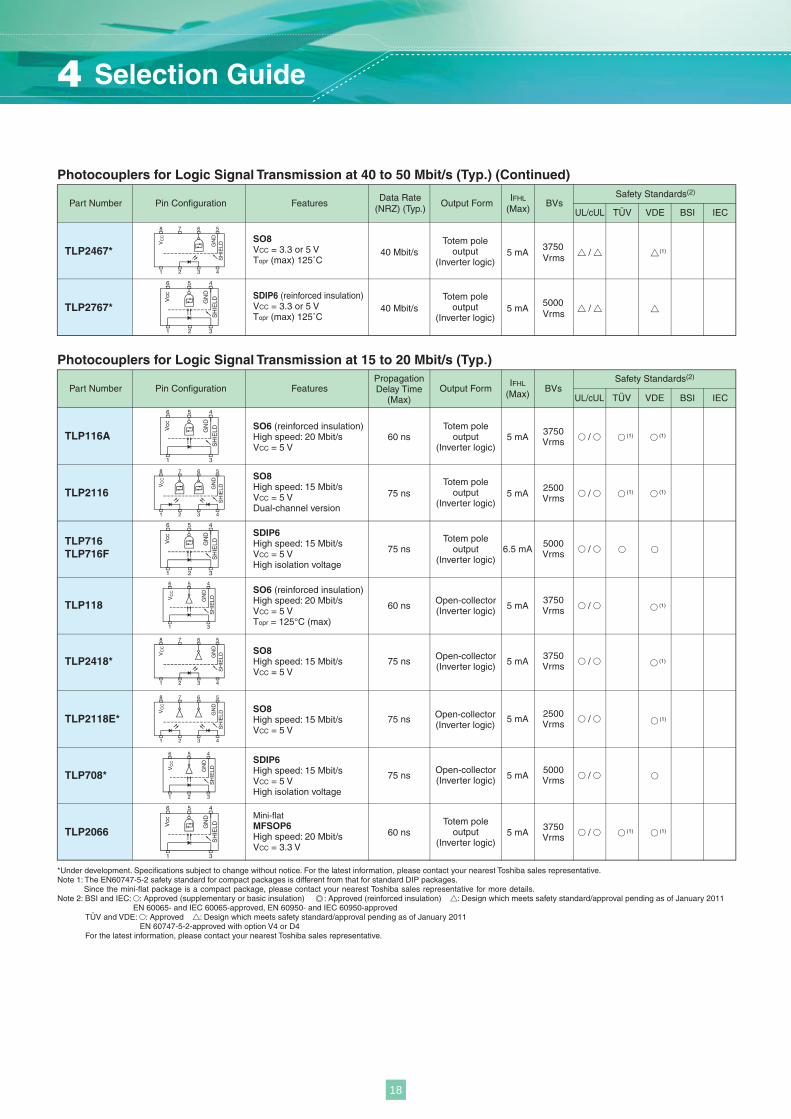
Photocouplers for Logic Signal Transmission at 15 to 20 Mbit/s (Typ.)
SO6 (reinforced insulation)High speed: 20 Mbit/sVCC = 5 V
SO6 (reinforced insulation)High speed: 20 Mbit/sVCC = 5 VTopr = 125°C (max)
TLP116A (1)60 ns
60 ns
75 ns
3750Vrms
Totem poleoutput
(Inverter logic)5 mA
5 mA
/
(1) /
(1)
SDIP6High speed: 15 Mbit/sVCC = 5 VHigh isolation voltage
TLP716TLP716F 75 ns
Totem poleoutput
(Inverter logic)6.5 mA
5000Vrms /
/
Mini-flatMFSOP6High speed: 20 Mbit/sVCC = 3.3 V
TLP2066 3750Vrms60 ns
Totem poleoutput
(Inverter logic)5 mA
SO8High speed: 15 Mbit/sVCC = 5 VDual-channel version
(1)
(1)
(1)
(1) / (1)
(1)
SDIP6High speed: 15 Mbit/sVCC = 5 VHigh isolation voltage
5000Vrms
2500Vrms
75 nsOpen-collector(Inverter logic) 5 mA /
/
TLP2116Totem pole
output(Inverter logic)
3750Vrms
2500Vrms
75 ns 5 mA /
/
SO8High speed: 15 Mbit/sVCC = 5 V
Open-collector(Inverter logic)
3750Vrms
TLP2118E*
TLP708*
TLP2418*
TLP118 5 mA
5 mA
Open-collector(Inverter logic)
Output FormVDE BSI IECUL/cUL TÜV
Part Number Pin Configuration Features BVsSafety Standards(2)Propagation
Delay Time(Max)
IFHL
(Max)
Photocouplers for Logic Signal Transmission at 40 to 50 Mbit/s (Typ.) (Continued)
Output FormVDE BSI IECUL/cUL TÜV
Part Number Pin Configuration Features BVsSafety Standards(2)
Data Rate(NRZ) (Typ.)
IFHL
(Max)
SO8High speed: 15 Mbit/sVCC = 5 V
TLP2767* 5000Vrms
40 Mbit/sTotem pole
output(Inverter logic)
75 ns Open-collector(Inverter logic)
5 mASDIP6 (reinforced insulation)VCC = 3.3 or 5 VTopr (max) 125˚C
/
SO8VCC = 3.3 or 5 VTopr (max) 125˚C
TLP2467* 3750Vrms
40 Mbit/sTotem pole
output(Inverter logic)
5 mA (1)
4 Selection Guide
18
VC
C
GN
D
6
1
5
2
4
3
VC
C
8
1
6 5
43
7
2
SH
IELDG
ND
VC
C
8
1
6 5
43
7
2
SH
IELDG
ND
VC
C
8
1
6 5
43
7
2
GN
DS
HIE
LD
6
1
5 4
3
Vcc
GN
D
VC
C
GN
D
8
1
6 5
43
7
2
SH
IELD
6
1
5 4
3
SH
IELDV
CC
GN
D
VC
C
GN
D
8
1
6 5
43
7
2
SH
IELD
VC
C
GN
D
8
1
6 5
43
7
2
SH
IELD
SH
IELD
6
1
5 4
32
Vcc
GN
D
6
1
5 4
32
SH
IELDV
CC
GN
D
VC
C
GN
D
8
1
6 5
43
7
2
SH
IELD
VC
C
GN
D
8
1
6 5
43
7
2
SH
IELD
15 Mbit/sTLP2166ATotem pole
output(Inverter logic)
2500Vrms
5000Vrms
5000Vrms
3 mA
SO8Propagation delay time: 75 nsVCC = 3.3 VDual-channel version
/
/
SO8VCC = 3.3 or 5 VTopr = 125˚C (max)Dual-channel version
3750Vrms
3750Vrms
3750Vrms
3750Vrms
3750Vrms
20 Mbit/s
20 Mbit/s
20 Mbit/s
20 Mbit/s
20 Mbit/s
20 Mbit/s
20 Mbit/s
Open-collector(Inverter logic) 5 mA
3.5 mA
5 mA
3.5 mA
5 mA
3.5 mA
5 mA
/ (1)
/
/
/
/
/
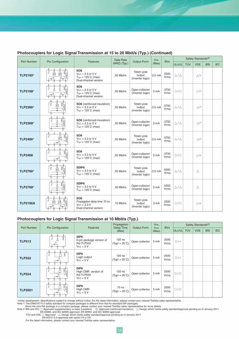
TLP2168*
TLP2366*
TLP2368*
TLP2466*
TLP2468
TLP2766*
TLP2768*
Photocouplers for Logic Signal Transmission at 15 to 20 Mbit/s (Typ.) (Continued)
Output FormVDE BSI IECUL/cUL TÜV
Part Number Pin Configuration Features BVsSafety Standards(2)
Data Rate(NRZ) (Typ.)
IFHL
(Max)
(1)
(1)
*Under development. Specifications subject to change without notice. For the latest information, please contact your nearest Toshiba sales representative.Note 1: The EN60747-5-2 safety standard for compact packages is different from that for standard DIP packages.
Since the mini-flat package is a compact package, please contact your nearest Toshiba sales representative for more details.Note 2: BSI and IEC: : Approved (supplementary or basic insulation) : Approved (reinforced insulation) : Design which meets safety standard/approval pending as of January 2011
EN 60065- and IEC 60065-approved, EN 60950- and IEC 60950-approvedTÜV and VDE: : Approved : Design which meets safety standard/approval pending as of January 2011
EN 60747-5-2-approved with option V4 or D4For the latest information, please contact your nearest Toshiba sales representative.
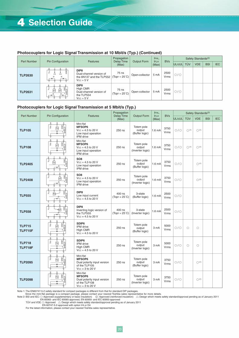
Photocouplers for Logic Signal Transmission at 10 Mbit/s (Typ.)
Output FormVDE BSI IECUL/cUL TÜV
Part Number Pin Configuration Features BVsSafety Standards(2)Propagation
Delay Time(Max)
IFHL,IFLH
(Max)
DIP8High CMRVCC = 5 V
/ –
/
/
DIP66-pin package version of the TLP552VCC = 5 V
TLP513 5 mA
DIP8Logic outputVCC = 5 V
TLP552 5 mA
DIP8High CMR version of the TLP552VCC = 5 V
2500Vrms
/ –2500Vrms
TLP554 5 mA
TLP2601
120 ns(Topr = 25˚C)
120 ns(Topr = 25˚C)
75 ns(Topr = 25˚C)
120 ns(Topr = 25˚C)
Open-collector
Open-collector
Open-collector
Open-collector 5 mA2500Vrms
2500Vrms
Open-collector(Inverter logic)
SO6 (reinforced insulation)VCC = 3.3 or 5 VTopr = 125˚C (max)
SO6 (reinforced insulation)VCC = 3.3 or 5 VTopr = 125˚C (max)
SO8VCC = 3.3 or 5 VTopr = 125˚C (max)
SO8VCC = 3.3 or 5 VTopr = 125˚C (max)
SDIP6VCC = 3.3 or 5 VTopr = 125˚C (max)
SDIP6VCC = 3.3 or 5 VTopr = 125˚C (max)
Totem poleoutput
(Inverter logic)
Open-collector(Inverter logic)
Totem poleoutput
(Inverter logic)
Open-collector(Inverter logic)
Totem poleoutput
(Inverter logic)
2500Vrms3.5 mA (1)
(1)
(1)
(1)
/ TLP2160*
SO8VCC = 3.3 or 5 VTopr = 125˚C (max)Dual-channel version
20 Mbit/sTotem pole
output(Inverter logic)
19
SH
IELD
6
1 2
5 4
3
Vcc
GN
D
SH
IELD
6
1 2
5 4
3
Vcc
GN
D
VC
C
8
1
6 5
43
7
2
SH
IELDG
ND
VC
C
8
1
6 5
43
7
2
SH
IELDG
ND
SH
IELD
6
1
5 4
3
Vcc
GN
D
SH
IELD
6
1
5 4
3
Vcc
GN
D
VC
C
GN
D
8
1
6 5
43
7
2
SH
IELD
SH
IELD
6
1
5 4
3
Vcc
GN
D
SH
IELD
6
1
5 4
3
Vcc
GN
D
VC
C
GN
D
8
1
6 5
43
7
2
SH
IELD
8
1
6 5
43
7
2
VC
C
GN
D
VC
C
GN
D
8
1
6 5
43
7
2
SH
IELD
Note 1: The EN60747-5-2 safety standard for compact packages is different from that for standard DIP packages.Since the mini-flat package is a compact package, please contact your nearest Toshiba sales representative for more details.
Note 2: BSI and IEC: : Approved (supplementary or basic insulation) : Approved (reinforced insulation) : Design which meets safety standard/approval pending as of January 2011EN 60065- and IEC 60065-approved, EN 60950- and IEC 60950-approved
TÜV and VDE: : Approved : Design which meets safety standard/approval pending as of January 2011EN 60747-5-2-approved with option V4 or D4
For the latest information, please contact your nearest Toshiba sales representative.
1.6 mA (1)
SO8VCC = 4.5 to 20 VLow input operationIPM drive
/ 250 nsTotem pole
output(Inverter logic)
3750Vrms
Output FormVDE BSI IECUL/cUL TÜV
Part Number Pin Configuration Features BVsSafety Standards(2)Propagation
Delay Time(Max)
Photocouplers for Logic Signal Transmission at 5 Mbit/s (Typ.) IFHL,IFLH
(Max)
SDIP6IPM driveHigh CMRVCC = 4.5 to 20 V
SDIP6IPM driveHigh CMRVCC = 4.5 to 20 V
Totem poleoutput
(Inverter logic)
TLP718TLP718F
TLP715TLP715F
5000Vrms
Totem poleoutput
(Buffer logic)3 mA
3 mA
5000Vrms
/
/
DIP8Inverting logic version of the TLP555VCC = 4.5 to 20 V
2500VrmsTLP558 /
2500Vrms
/ DIP8Low input currentVCC = 4.5 to 20 V
TLP555
TLP2408
1.6 mA400 ns(Topr = 25˚C)
250 ns
250 ns
3-state(Inverter logic)
1.6 mA400 ns
(Topr = 25˚C)3-state
(Buffer logic)
3 mA
Mini-flatMFSOP6Dual polarity input version of the TLP105VCC = 3 to 20 V
TLP2095Totem pole
output(Buffer logic)
Totem poleoutput
(Inverter logic)
3750Vrms
3750Vrms
Mini-flatMFSOP6Dual polarity input version of the TLP108VCC = 3 to 20 V
TLP2098 3 mA250 ns
250 ns / (1)
/ (1)
(1)1.6 mA (1)
Mini-flatMFSOP6VCC = 4.5 to 20 VLow input operationIPM drive
/ TLP105 250 nsTotem pole
output(Buffer logic)
3750Vrms
1.6 mA (1)
SO8VCC = 4.5 to 20 VLow input operationIPM drive
/ 250 nsTotem pole
output(Buffer logic)
3750Vrms
(1)1.6 mA (1)
Mini-flatMFSOP6VCC = 4.5 to 20 VLow input operationIPM drive
/ TLP108 250 nsTotem pole
output(Inverter logic)
3750Vrms
TLP2405
/
/ Open-collector
Open-collector
DIP8Dual-channel version of the 6N137 and the TLP552VCC = 5 V
DIP8High CMRDual-channel version of the TLP554VCC = 5 V
2500Vrms
2500Vrms
TLP263075 ns
(Topr = 25˚C)
TLP263175 ns
(Topr = 25˚C)
5 mA
5 mA
Photocouplers for Logic Signal Transmission at 10 Mbit/s (Typ.) (Continued)
Output FormVDE BSI IECUL/cUL TÜV
Part Number Pin Configuration Features BVsSafety Standards(2)Propagation
Delay Time(Max)
IFHL,IFLH
(Max)
4 Selection Guide
20
VC
C
8
1
6 5
43
7
2
SH
IELDG
ND
VC
C
GN
D
8
1
6 5
43
7
2
SH
IELD
VC
C
GN
D
8
1
6 5
43
7
2
SH
IELD
SH
IELD
6
1
5 4
3
8
1
6 5
43
7
2
SH
IELD
8
1
6 5
43
7
2
SH
IELD
6
1
5
2
4
3
8
1
6 5
43
7
2
8
1
6 5
43
7
2
8
1
6 5
43
7
2
SH
IELD
321
6 5 4
8
1
6 5
43
7
2
8
1
6 5
43
7
2
(1)
(1)
1.6 mA
1.6 mA
(1)
(1)
SO8Dual-channel version forthe TLP105VCC = 4.5 to 20 V
SO8Dual-channel version forthe TLP108VCC = 4.5 to 20 V
/
/
TLP2105
TLP2108
Totem poleoutput
(Buffer logic)
Totem poleoutput
(Inverter logic)
3750Vrms
3750Vrms
2500Vrms
/
DIP8Low input currentVCC = 4.5 to 20 V
TLP2200 1.6 mA400 ns
250 ns
250 ns
3-state(Buffer logic)
SO6 (reinforced insulation)TLP109
TLP2409
3750Vrms1 Mbit/s 20% (min) 16 mA (1)/
SO8Topr = 125˚C(max)SO8 version of the TLP109
16 mA1 Mbit/s 20% (min) / (1)3750Vrms
Note 1: The EN60747-5-2 safety standard for compact packages is different from that for standard DIP packages.Since the mini-flat package is a compact package, please contact your nearest Toshiba sales representative for more details.
Note 2: BSI and IEC: : Approved (supplementary or basic insulation) : Approved (reinforced insulation) : Design which meets safety standard/approval pending as of January 2011EN 60065- and IEC 60065-approved, EN 60950- and IEC 60950-approved
TÜV and VDE: : Approved : Design which meets safety standard/approval pending as of January 2011EN 60747-5-2-approved with option V4 or D4
For the latest information, please contact your nearest Toshiba sales representative.
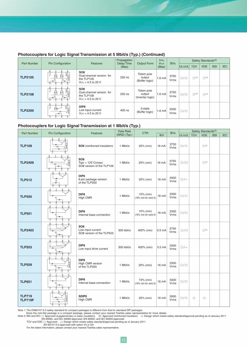
Photocouplers for Logic Signal Transmission at 1 Mbit/s (Typ.)
CTRVDE BSI IECUL/cUL TÜV
Part Number Pin Configuration Features BVsSafety Standards(2)Data Rate
(NRZ) (Typ.) @IF
DIP66-pin package version of the TLP550
DIP8High CMR
TLP512
TLP550
2500Vrms
1 Mbit/s 20% (min) 16 mA / –
10% (min)(19% min for rank 0)
2500Vrms1 Mbit/s 16 mA /
DIP8Internal base connectionTLP551
TLP2403
2500Vrms
10% (min)(19% min for rank 0)
1 Mbit/s 16 mA /
DIP8Low input drive current
2500VrmsTLP553 300 kbit/s 400% (min) 0.5 mA / –
DIP8Internal base connectionTLP651
10% (min)(19% min for rank 0)
1 Mbit/s 16 mA /
SDIP6High CMR
TLP719TLP719F
5000Vrms
5000Vrms
1 Mbit/s 20% (min) 16 mA /
DIP8High CMR version of the TLP550
2500VrmsTLP559 20% (min) 16 mA / 1 Mbit/s
SO8Low input currentSO8 version of the TLP553
0.5 mA300 kbit/s 400% (min) / (1)3750Vrms
Photocouplers for Logic Signal Transmission at 5 Mbit/s (Typ.) (Continued)
Output FormVDE BSI IECUL/cUL TÜV
Part Number Pin Configuration FeaturesSafety Standards(2)Propagation
Delay Time(Max)
IFHL,IFLH
(Max)BVs
21
SH
IELD
6
1
5 4
3
8
1
6 5
43
7
2
SH
IELD
SH
IELD
6
1
5 4
3
SH
IELD
6
1
5 4
38
1
7 6 5
42 3
SH
IELD
8
1
7 6 5
42 3
SH
IELD
8
1
6 5
43
7
2
8
1
6 5
43
7
2
8
1
6 5
43
7
2
8
1
6 5
43
7
2
8
1
6 5
43
7
2
SH
IELD
*Under development. Specifications subject to change without notice. For the latest information, please contact your nearest Toshiba sales representative.Note 1: The EN60747-5-2 safety standard for compact packages is different from that for standard DIP packages.
Since the mini-flat package is a compact package, please contact your nearest Toshiba sales representative for more details.Note 2: BSI and IEC: : Approved (supplementary or basic insulation) : Approved (reinforced insulation) : Design which meets safety standard/approval pending as of January 2011
EN 60065- and IEC 60065-approved, EN 60950- and IEC 60950-approvedTÜV and VDE: : Approved : Design which meets safety standard/approval pending as of January 2011
EN 60747-5-2-approved with option V4 or D4For the latest information, please contact your nearest Toshiba sales representative.
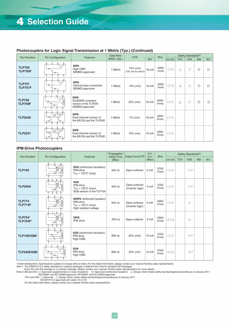
IPM-Drive Photocouplers
Output Form/CTRVDE BSI IECUL/cUL TÜV
Part Number Pin Configuration Features BVsSafety Standards(2)Propagation
Delay Time(Max)
IFHL,IFLH
(Max)
SO8IPM driveHigh CMR
3750Vrms800 ns 20% (min) 10 mA
SO6 (reinforced insulation)IPM driveHigh CMR
3750Vrms25% (min) 10 mA / (1)
(1)
800 ns
5 mASO6 (reinforced insulation)IPM driveTopr = 125°C (max)
TLP104 550 ns Open-collector / 3750Vrms
5 mASDIP6 (reinforced insulation)IPM driveTopr = 125°C (max)High isolation voltage
550 ns Open-collector(Inverter logic)
/ 5000Vrms
5 mADIP8IPM drive
TLP754*TLP754F*
TLP109(IGM)
TLP2409(IGM)
TLP714TLP714F
TLP2404
Open-collector5000Vrms550 ns /
/ (1)
5 mA (1)
SO8IPM driveTopr = 125°C (max)SO8 version of the TLP104
/ 550 nsOpen-collector(Inverter logic)
3750Vrms
DIP8High CMRSEMKO-approved
DIP8Internal base connectionSEMKO-approved
5000Vrms
1 Mbit/s 10% (min) 16 mA
TLP750TLP750F
TLP751TLP751F
10% (min)(19% min for rank 0)
1 Mbit/s 16 mA /
5000Vrms
/
DIP8IEC60950-compliantversion of the TLP559SEMKO-approved
TLP759TLP759F
5000Vrms1 Mbit/s 20% (min) 16 mA /
/ DIP8Dual-channel version of the 6N135 and the TLP550
DIP8Dual-channel version of the 6N136 and the TLP550
TLP2530 1 Mbit/s 7% (min)
TLP2531 1 Mbit/s 19% (min)
16 mA
/ 16 mA
2500Vrms
2500Vrms
Photocouplers for Logic Signal Transmission at 1 Mbit/s (Typ.) (Continued)
CTRVDE BSI IECUL/cUL TÜV
Part Number Pin Configuration Features BVsSafety Standards(2)Data Rate
(NRZ) (Typ.) @IF
4 Selection Guide
22
8
1
6 5
43
7
2
SH
IELD
8
1
6 5
43
7
2
SH
IELD
VC
C
GN
D
8
1
6 5
43
7
2
8
1
6 5
43
7
2
8
1
6 5
43
7
2
8
1
6 5
43
7
2
8
1
6 5
43
7
2
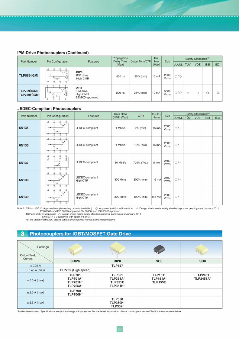
DIP8IPM driveHigh CMR
TLP559(IGM) 2500Vrms
800 ns 25% (min) 10 mA /
5000Vrms25% (min) 10 mA
DIP8IPM driveHigh CMRSEMKO-approved
TLP759(IGM)TLP759F(IGM) / 800 ns
± 0.25 A
± 0.45 A (max)
± 0.6 A (max)
± 2.0 A (max)
± 2.5 A (max)
Output PeakCurrent
Package
SDIP6 DIP8 SO6 SO8
TLP705 (High speed)
TLP701
TLP700H*TLP700
TLP701A*TLP701H*TLP705A*
TLP350H*TLP352*
TLP151*
TLP557
TLP351
TLP351ETLP351A*
TLP351H*TLP155ETLP151A*
TLP350
TLP2451TLP2451A*
*Under development. Specifications subject to change without notice. For the latest information, please contact your nearest Toshiba sales representative.
Photocouplers for IGBT/MOSFET Gate Drive3
Note 2: BSI and IEC: : Approved (supplementary or basic insulation) : Approved (reinforced insulation) : Design which meets safety standard/approval pending as of January 2011EN 60065- and IEC 60065-approved, EN 60950- and IEC 60950-approved
TÜV and VDE: : Approved : Design which meets safety standard/approval pending as of January 2011EN 60747-5-2-approved with option V4 or D4
For the latest information, please contact your nearest Toshiba sales representative.
JEDEC-Compliant Photocouplers
CTRVDE BSI IECUL/cUL TÜV
Part Number Pin Configuration Features BVsSafety Standards(2)Data Rate
(NRZ) (Typ.)IFHL, IFLH
(Max)
JEDEC-compliant
JEDEC-compliant
JEDEC-compliant
JEDEC-compliantHigh CTR
JEDEC-compliantHigh CTR
6N135 7% (min)
2500Vrms
6N136 19% (min)
2500Vrms
2500Vrms
2500Vrms
2500Vrms
6N138 300 kbit/s 300% (min) 1.6 mA
400% (min) 0.5 mA
1 Mbit/s 16 mA
6N137 10 Mbit/s 700% (Typ.) 5 mA
/ –
300 kbit/s / –
/ –
1 Mbit/s 16 mA / –
/ –
6N139
IPM-Drive Photocouplers (Continued)
Output Form/CTRVDE BSI IECUL/cUL TÜV
Part Number Pin Configuration Features BVsSafety Standards(2)Propagation
Delay Time(Max)
IFHL,IFLH
(Max)
23
6
1
5 4
3
6
1
5 4
3
8
1
6 5
43
7
2
8
1
6 5
43
7
2
8
1
6 5
43
7
2
8
1
6 5
43
7
2
8
1
6 5
43
7
2
8
1
6 5
43
7
2
8
1
6 5
43
7
2
*Under development. Specifications subject to change without notice. For the latest information, please contact your nearest Toshiba sales representative.Note 1: The EN60747-5-2 safety standard for compact packages is different from that for standard DIP packages.
Since the mini-flat package is a compact package, please contact your nearest Toshiba sales representative for more details.Note 2: BSI and IEC: : Approved (supplementary or basic insulation) : Approved (reinforced insulation) : Design which meets safety standard/approval pending as of January 2011
EN 60065- and IEC 60065-approved, EN 60950- and IEC 60950-approvedTÜV and VDE: : Approved : Design which meets safety standard/approval pending as of January 2011
EN 60747-5-2-approved with option V4 or D4For the latest information, please contact your nearest Toshiba sales representative.
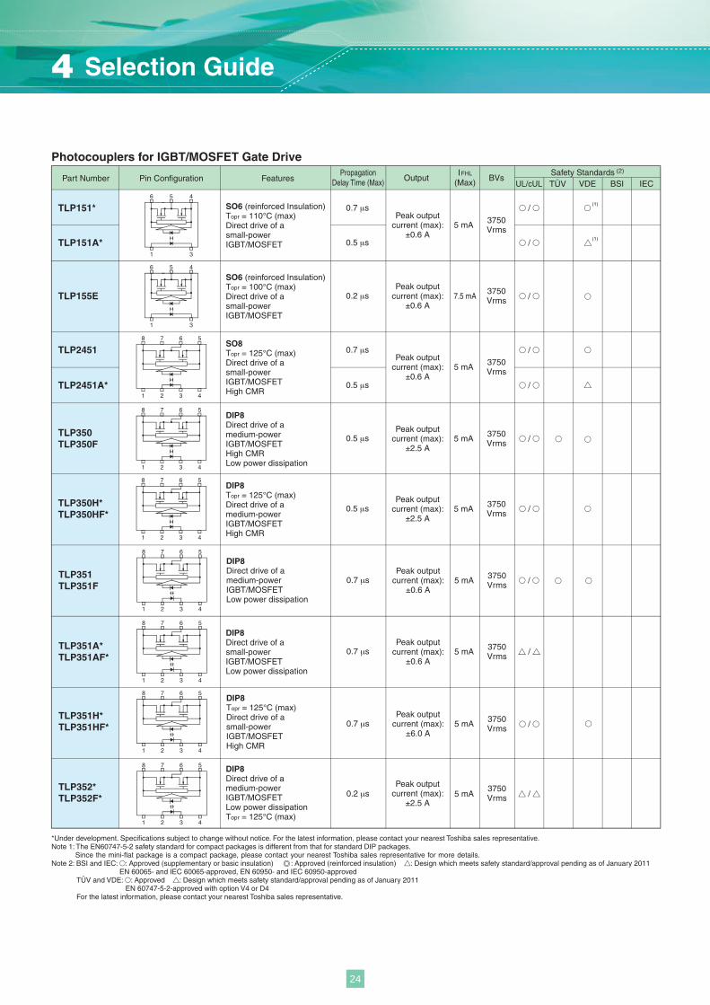
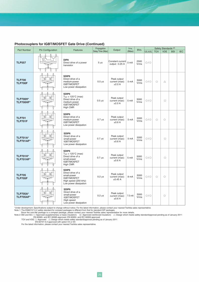
Photocouplers for IGBT/MOSFET Gate Drive
OutputVDE BSI IECUL/cUL TÜV
Part Number Pin Configuration Features BVsSafety Standards (2)Propagation
Delay Time (Max)IFHL
(Max)
SO6 (reinforced Insulation)Topr = 110°C (max)Direct drive of a small-power IGBT/MOSFET
TLP151*
TLP155E
TLP2451
3750Vrms
3750Vrms
0.7 μs
0.2 μs
Peak outputcurrent (max):
±0.6 A
Peak outputcurrent (max):
±0.6 A
5 mA
7.5 mA
DIP8Direct drive of a medium-power IGBT/MOSFETHigh CMRLow power dissipation
SO8Topr = 125°C (max)Direct drive of a small-power IGBT/MOSFETHigh CMR
TLP350TLP350F
TLP350H*TLP350HF*
3750Vrms
0.5 μsPeak output
current (max):±2.5 A
5 mA /
DIP8Topr = 125°C (max)Direct drive of a medium-power IGBT/MOSFETHigh CMR
3750Vrms
0.5 μsPeak output
current (max):±2.5 A
Peak outputcurrent (max):
±2.5 A
5 mA /
/
/
/
/
TLP151A* 0.5 μs /
/
(1)
(1)
3750Vrms
0.7 μsPeak output
current (max):±0.6 A
5 mA
/
TLP2451A* 0.5 μs /
DIP8Direct drive of a medium-power IGBT/MOSFETLow power dissipation
TLP351TLP351F
TLP351A*TLP351AF*
TLP351H*TLP351HF*
TLP352*TLP352F*
3750Vrms
3750Vrms
0.7 μs
0.7 μs
Peak outputcurrent (max):
±0.6 A
Peak outputcurrent (max):
±0.6 A
5 mA
5 mA
/
3750Vrms
3750Vrms
0.7 μs
0.2 μs
Peak outputcurrent (max):
±6.0 A5 mA
5 mA
DIP8Topr = 125°C (max)Direct drive of a small-power IGBT/MOSFETHigh CMR
SO6 (reinforced Insulation)Topr = 100°C (max)Direct drive of a small-power IGBT/MOSFET
DIP8Direct drive of a small-power IGBT/MOSFETLow power dissipation
DIP8Direct drive of a medium-power IGBT/MOSFETLow power dissipationTopr = 125°C (max)
4 Selection Guide
24
8
1
6 5
43
7
2
6
1 2
5 4
3
6
1 2
5 4
3
6
1 2
5 4
3
6
1 2
5 4
3
6
1 2
5 4
3
6
1 2
5 4
3
6
1 2
5 4
3
*Under development. Specifications subject to change without notice. For the latest information, please contact your nearest Toshiba sales representative.Note 1: The EN60747-5-2 safety standard for compact packages is different from that for standard DIP packages.
Since the mini-flat package is a compact package, please contact your nearest Toshiba sales representative for more details.Note 2: BSI and IEC: : Approved (supplementary or basic insulation) : Approved (reinforced insulation) : Design which meets safety standard/approval pending as of January 2011
EN 60065- and IEC 60065-approved, EN 60950- and IEC 60950-approvedTÜV and VDE: : Approved : Design which meets safety standard/approval pending as of January 2011
EN 60747-5-2-approved with option V4 or D4For the latest information, please contact your nearest Toshiba sales representative.
Photocouplers for IGBT/MOSFET Gate Drive (Continued)
OutputVDE BSI IECUL/cUL TÜV
Part Number Pin Configuration Features BVsSafety Standards (2)Propagation
Delay Time (Max)IFHL
(Max)
DIP8Direct drive of a power transistor
TLP557 2500Vrms
5 μs Constant currentoutput : 0.25 A 5 mA /
SDIP6Topr = 125°C (max)Direct drive of a medium-power IGBT/MOSFETHigh CMR
5000Vrms
0.5 μsPeak output
current (max):±2.0 A
5 mA /
SDIP6Topr = 125°C (max)Direct drive of a small-power IGBT/MOSFETHigh CMR
5000Vrms
0.7 μs
0.7 μs
Peak outputcurrent (max):
±0.6 A5 mA /
/
/
SDIP6Direct drive of a medium-power IGBT/MOSFETLow power dissipation
TLP701TLP701F
TLP701H*TLP701HF*
TLP705A*TLP705AF*
TLP701A*TLP701AF*
TLP705TLP705F
SDIP6Direct drive of a medium-power IGBT/MOSFETLow power dissipation
TLP700TLP700F
TLP700H*TLP700HF*
5000Vrms
5000Vrms
0.7 μsPeak output
current (max):±0.6 A
Peak outputcurrent (max):
±0.6 A
5 mA
5 mA
SDIP6Direct drive of a small-power IGBT/MOSFETHigh speed (250 kHz)Low power dissipation
8 mA
7.5 mA
5000Vrms
5000Vrms
0.2 μs
0.2 μs
Peak outputcurrent (max):
±0.45 A
5000Vrms
0.5 μsPeak output
current (max):±2.0 A
5 mA
/
/
/
SDIP6Direct drive of a small-power IGBT/MOSFETLow power dissipation
SDIP6Direct drive of a small-power IGBT/MOSFETHigh speed Low power dissipation
Peak outputcurrent (max):
±0.6 A
25
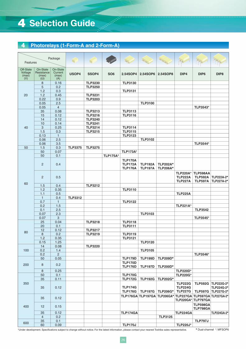
Photorelays (1-Form-A and 2-Form-A)4
20
40
60
80
100
50
350
200
400
600
85
1.21.2
0.05
351514103
1.50.130.06
2
2
0.70.20.1
2520128
1.20.1514
50
35
35
35
12
354
60
0.160.20.30.45
2.50.05 4
0.080.120.120.140.25
2.50.06 3.5
0.31
50 0.0750 0.1
0.4
0.5
1
0.07 3
1.5
0.2 1.40.2 2
2.5
0.040.10.120.20.351.250.08
0.05
0.2
0.11
0.12
0.12
0.15
0.120.2
0.09
TLP3230TLP3250
TLP32310.22 0.9 TLP3203
TLP3213TLP3216TLP3240TLP3241TLP3214TLP3215
TLP3375
TLP3123
TLP3217
TLP3220
TLP3130
TLP3131
TLP3113TLP3116
TLP3114TLP3115
TLP172ATLP170A
TLP176A
TLP3122
TLP3105
TLP3118TLP3218TLP3111
TLP3119TLP3219TLP3121
TLP179D
TLP176D8
0.258
TLP170D
TLP172G50 0.1 TLP170G
TLP176GTLP174G
TLP176GA
TLP174GA
TLP3100
TLP3102
TLP192ATLP197A
TLP3120
TLP199D
TLP197D
TLP192G
TLP197GTLP197GA
TLP202A◆
TLP173A†
1.5 0.3 TLP3275
TLP206A◆
TLP209D◆
TLP200D◆
TLP202G◆
TLP206G◆
TLP220J*
TLP220GA*TLP206GA◆
TLP3125
TLP221A*
TLP220D*TLP220G*
TLP222ATLP227A
TLP222G
TLP227GTLP224G
TLP227GA
TLP224GA
TLP598AATLP220A*TLP592ATLP597A
TLP3542
TLP3544*
TLP3543*
TLP3545*
TLP3546*
0.07 2.3 TLP3103
TLP592G
TLP597GTLP597GATLP797GATLP598GATLP798GA
TLP170J35 0.1 TLP797J
TLP222A-2◆
TLP227A-2◆
0.4 TLP331211.1 0.5 TLP225A1.2 0.35 TLP31101.5 0.4 TLP3212
TLP222G-2◆
TLP227G-2◆
TLP224G-2◆
TLP227GA-2◆
TLP224GA-2◆
DIP6DIP42.54SOP82.54SOP62.54SOP4SSOP4 SO6USOP4 DIP8Off-StateVoltage(max)
(V)
On-StateResistance
(max)(Ω)
On-StateCurrent(max)
(A)
PackageFeatures
◆ Dual-channel †: MFSOP6*Under development. Specifications subject to change without notice. For the latest information, please contact your nearest Toshiba sales representative.
TLP175A*
4 Selection Guide
26
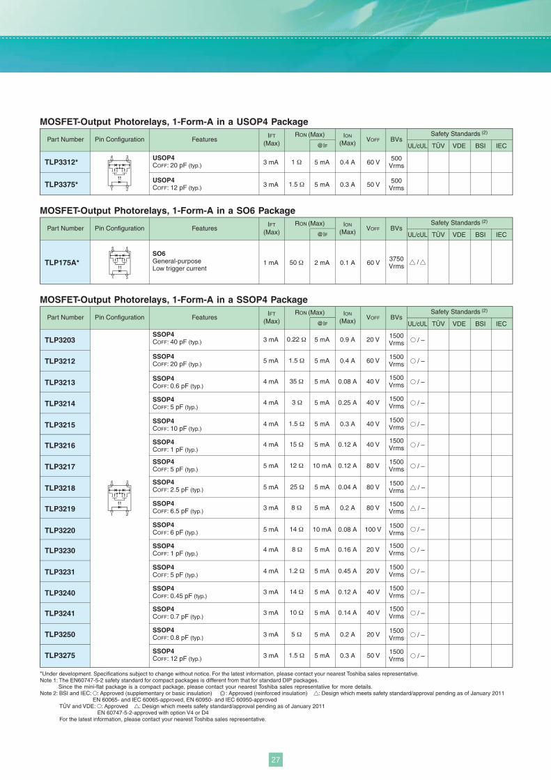
1
4 3
2
1
4 3
2
1
6 4
3
MOSFET-Output Photorelays, 1-Form-A in a USOP4 Package
Part Number Pin Configuration FeaturesRON (Max)
VDE BSI IECUL/cUL TÜVBVsVOFF
IFT
(Max) @IF
ION
(Max)Safety Standards (2)
IEC
500Vrms60 VTLP3312* 1 Ω3 mA 5 mA 0.4 A
USOP4COFF: 20 pF (typ.)
500Vrms50 VTLP3375* 1.5 Ω3 mA 5 mA
50 Ω 2 mA
0.3 AUSOP4COFF: 12 pF (typ.)
MOSFET-Output Photorelays, 1-Form-A in a SO6 Package
Part Number Pin Configuration FeaturesRON (Max)
VDE BSI IECUL/cUL TÜVBVsVOFF
IFT
(Max) @IF
ION
(Max)Safety Standards (2)
3750Vrms60 VTLP175A* 1 mA 0.1 A
*Under development. Specifications subject to change without notice. For the latest information, please contact your nearest Toshiba sales representative.Note 1: The EN60747-5-2 safety standard for compact packages is different from that for standard DIP packages.
Since the mini-flat package is a compact package, please contact your nearest Toshiba sales representative for more details.Note 2: BSI and IEC: : Approved (supplementary or basic insulation) : Approved (reinforced insulation) : Design which meets safety standard/approval pending as of January 2011
EN 60065- and IEC 60065-approved, EN 60950- and IEC 60950-approvedTÜV and VDE: : Approved : Design which meets safety standard/approval pending as of January 2011
EN 60747-5-2-approved with option V4 or D4For the latest information, please contact your nearest Toshiba sales representative.
MOSFET-Output Photorelays, 1-Form-A in a SSOP4 Package
Part Number Pin Configuration FeaturesRON (Max)
VDE BSI IECUL/cUL TÜVBVsVOFF
IFT
(Max) @IF
ION
(Max)Safety Standards (2)
SSOP4COFF: 20 pF (typ.)
SSOP4COFF: 40 pF (typ.)
/ –
/ –
TLP3212
TLP3203
5 mA 1.5 Ω 5 mA 0.4 A
3 mA 0.22 Ω 5 mA 0.9 A 20 V
60 V
40 V
40 V
40 V
40 V
SSOP4COFF: 5 pF (typ.)
SSOP4COFF: 2.5 pF (typ.)
SSOP4COFF: 6.5 pF (typ.) / –
/
TLP3219
/ –TLP3218
TLP3217 / –80 V
80 V
80 V
20 V
20 V
3 mA
5 mA
5 mA
8 Ω
12 Ω
25 Ω
5 mA
10 mA
5 mA
0.2 A
0.12 A
0.04 A
IEC
SSOP4COFF: 6 pF (typ.) / –TLP3220 100 V5 mA 14 Ω 10 mA 0.08 A
/ –TLP3213 35 Ω4 mA 5 mA 0.08 ASSOP4COFF: 0.6 pF (typ.)
/ –TLP3214 3 Ω4 mA 5 mA 0.25 ASSOP4COFF: 5 pF (typ.)
TLP3215 1.5 Ω4 mA 5 mA 0.3 ASSOP4COFF: 10 pF (typ.)
/ –
TLP3216 15 Ω4 mA 5 mA 0.12 ASSOP4COFF: 1 pF (typ.)
/ –
TLP3230 / –8 Ω4 mA 5 mA 0.16 ASSOP4COFF: 1 pF (typ.)
TLP3231 / –1.2 Ω4 mA 5 mA 0.45 ASSOP4COFF: 5 pF (typ.)
/ –TLP3240 14 Ω3 mA 5 mA 0.12 ASSOP4COFF: 0.45 pF (typ.)
/ –
1500Vrms
1500Vrms
1500Vrms
1500Vrms
1500Vrms
1500Vrms
1500Vrms
1500Vrms
1500Vrms
1500Vrms
1500Vrms
1500Vrms
1500Vrms
1500Vrms
40 V
40 VTLP3241 10 Ω3 mA 5 mA 0.14 ASSOP4COFF: 0.7 pF (typ.)
/ –1500Vrms20 VTLP3250 5 Ω3 mA 5 mA 0.2 A
SSOP4COFF: 0.8 pF (typ.)
/ –1500Vrms50 VTLP3275 1.5 Ω3 mA 5 mA 0.3 A
SSOP4COFF: 12 pF (typ.)
SO6General-purposeLow trigger current
27
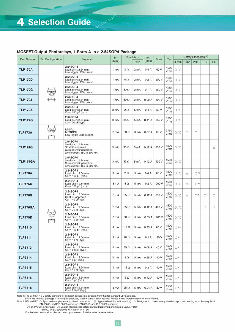
1
4 3
2
1
4 3
2
1
6 4
3
TLP176A 1500Vrms
(1)/2 Ω3 mA 5 mA 0.4 A2.54SOP4Lead pitch: 2.54 mmCOFF: 130 pF (typ.)
60 V
TLP173A3750Vrms /50 Ω2 mA 3 mA 0.07 A
Mini-flatMFSOP6Low trigger LED current
60 V
1500Vrms / –TLP3110 1.2 Ω4 mA 5 mA 0.35 A
2.54SOP4Lead pitch: 2.54 mmCOFF: 100 pF (typ.)
60 V
/ –
1500Vrms
TLP3116
/ –TLP3113 35 Ω4 mA 5 mA 40 V
1500Vrms40 V15 Ω4 mA 5 mA 0.12 A
0.08 A2.54SOP4Lead pitch: 2.54 mmCOFF: 0.6 pF (typ.)
2.54SOP4Lead pitch: 2.54 mmCOFF: 1 pF (typ.)
2.54SOP4Lead pitch: 2.54 mmCOFF: 2.5 pF (typ.)
/ –1500VrmsTLP3118 80 V3 mA 25 Ω 5 mA 0.04 A
2.54SOP4Lead pitch: 2.54 mmCOFF: 11 pF (typ.)
/ –1500VrmsTLP3111 80 V4 mA 20 Ω 5 mA 0.1 A
2.54SOP4Lead pitch: 2.54 mmCOFF: 15 pF (typ.)
/TLP179D1500Vrms200 V3 mA 50 Ω 5 mA 0.05 A
2.54SOP4Lead pitch: 2.54 mmCOFF: 100 pF (typ.)
TLP176D / (1)1500Vrms200 V3 mA 8 Ω 5 mA 0.2 A
/ –TLP3115
/ –TLP3114 1500Vrms40 V
1500Vrms40 V1.5 Ω4 mA 5 mA 0.3 A
3 Ω4 mA 5 mA 0.25 A2.54SOP4Lead pitch: 2.54 mmCOFF: 5 pF (typ.)
2.54SOP4Lead pitch: 2.54 mmCOFF: 10 pF (typ.)
Note 1: The EN60747-5-2 safety standard for compact packages is different from that for standard DIP packages.Since the mini-flat package is a compact package, please contact your nearest Toshiba sales representative for more details.
Note 2: BSI and IEC: : Approved (supplementary or basic insulation) : Approved (reinforced insulation) : Design which meets safety standard/approval pending as of January 2011EN 60065- and IEC 60065-approved, EN 60950- and IEC 60950-approved
TÜV and VDE: : Approved : Design which meets safety standard/approval pending as of January 2011EN 60747-5-2-approved with option V4 or D4
For the latest information, please contact your nearest Toshiba sales representative.
1500Vrms / (1)TLP176G 350 V35 Ω3 mA 5 mA 0.12 A
2.54SOP4Lead pitch: 2.54 mmSEMKO-approvedCOFF: 40 pF (typ.)
TLP176GA1500Vrms /400 V35 Ω3 mA 5 mA 0.12 A
2.54SOP4Lead pitch: 2.54 mmCOFF: 70 pF (typ.)
1500Vrms
1500Vrms
TLP174G /350 V
400 V
35 Ω3 mA 5 mA 0.12 A
2.54SOP4Lead pitch: 2.54 mmSEMKO-approvedCurrent-limiting functionLimit current: 150 to 300 mA
TLP174GA /35 Ω3 mA 5 mA 0.12 A2.54SOP4Lead pitch: 2.54 mmCurrent-limiting functionLimit current: 150 to 300 mA
Part Number Pin Configuration FeaturesRON (Max)
VDE BSI IECUL/cUL TÜVBVsVOFF
IFT
(Max) @IF
ION
(Max)Safety Standards (2)
MOSFET-Output Photorelays, 1-Form-A in a 2.54SOP4 Package
1500Vrms
1500Vrms
1500Vrms
1500Vrms
1500Vrms
1500Vrms
/60 VTLP170A 2 Ω1 mA 2 mA 0.4 A2.54SOP4Lead pitch: 2.54 mmLow trigger LED current
/200 VTLP170D 8 Ω1 mA 2 mA 0.2 A2.54SOP4Lead pitch: 2.54 mmLow trigger LED current
/350 VTLP170G 50 Ω1 mA 2 mA 0.1 A2.54SOP4Lead pitch: 2.54 mmLow trigger LED current
/600 V
60 V
TLP170J 60 Ω1 mA 2 mA 0.09 A2.54SOP4Lead pitch: 2.54 mmLow trigger LED current
TLP172A /2 Ω3 mA 5 mA 0.4 A2.54SOP4Lead pitch: 2.54 mmCOFF: 130 pF (typ.)
2.54SOP4Lead pitch: 2.54 mmCOFF: 30 pF (typ.)
/TLP172G 35 Ω3 mA 5 mA 0.11 A 350 V
4 Selection Guide
28
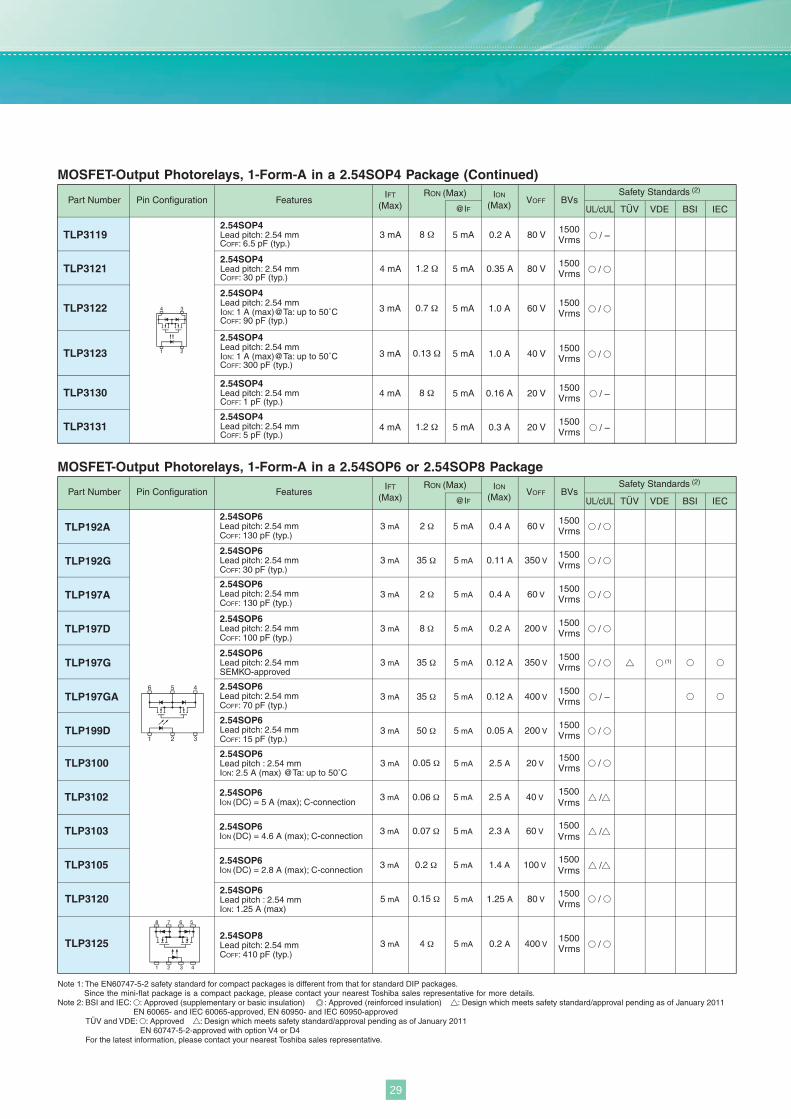
6
1
5 4
32
1
8 7 6 5
32 4
1
4 3
2
Note 1: The EN60747-5-2 safety standard for compact packages is different from that for standard DIP packages.Since the mini-flat package is a compact package, please contact your nearest Toshiba sales representative for more details.
Note 2: BSI and IEC: : Approved (supplementary or basic insulation) : Approved (reinforced insulation) : Design which meets safety standard/approval pending as of January 2011EN 60065- and IEC 60065-approved, EN 60950- and IEC 60950-approved
TÜV and VDE: : Approved : Design which meets safety standard/approval pending as of January 2011EN 60747-5-2-approved with option V4 or D4
For the latest information, please contact your nearest Toshiba sales representative.
MOSFET-Output Photorelays, 1-Form-A in a 2.54SOP6 or 2.54SOP8 Package
TLP192A1500Vrms /
2.54SOP6Lead pitch: 2.54 mmCOFF: 130 pF (typ.)
60 V
1500Vrms60 V
3 mA 2 Ω 5 mA 0.4 A
TLP197A /2.54SOP6Lead pitch: 2.54 mmCOFF: 130 pF (typ.)
3 mA 2 Ω 5 mA 0.4 A
2.54SOP6Lead pitch : 2.54 mmION: 1.25 A (max)
/TLP3120 1500Vrms80 V5 mA 0.15 Ω 5 mA 1.25 A
2.54SOP6Lead pitch: 2.54 mmCOFF: 15 pF (typ.)
TLP199D /1500Vrms200 V3 mA 50 Ω 5 mA 0.05 A
2.54SOP6Lead pitch: 2.54 mmCOFF: 100 pF (typ.)
TLP197D /8 Ω3 mA 5 mA 200 V0.2 A1500Vrms
1500Vrms /TLP192G 350 V35 Ω3 mA 5 mA 0.11 A
2.54SOP6Lead pitch: 2.54 mmCOFF: 30 pF (typ.)
1500Vrms / (1)TLP197G 350 V
TLP197GA / –1500Vrms400 V35 Ω3 mA 5 mA 0.12 A
2.54SOP6Lead pitch: 2.54 mmCOFF: 70 pF (typ.)
35 Ω3 mA 5 mA 0.12 A2.54SOP6Lead pitch: 2.54 mmSEMKO-approved
TLP3125 /1500Vrms400 V4 Ω3 mA 5 mA 0.2 A
2.54SOP8Lead pitch: 2.54 mmCOFF: 410 pF (typ.)
1500Vrms /TLP3100 20 V0.05 Ω 5 mA 2.5 A3 mA
2.54SOP6Lead pitch : 2.54 mmION: 2.5 A (max) @Ta: up to 50˚C
MOSFET-Output Photorelays, 1-Form-A in a 2.54SOP4 Package (Continued)
20 V
20 V
1500Vrms40 V
/1500Vrms0.7 Ω3 mA 5 mA 1.0 ATLP3122 60 V
/TLP3123 0.13 Ω3 mA 5 mA 1.0 A
1500Vrms
1500Vrms
/ –
TLP3131 / –1.2 Ω
8 Ω
4 mA
4 mA
5 mA
5 mATLP3130
0.3 A
0.16 A2.54SOP4Lead pitch: 2.54 mmCOFF: 1 pF (typ.)
2.54SOP4Lead pitch: 2.54 mmION: 1 A (max)@Ta: up to 50˚CCOFF: 90 pF (typ.)
2.54SOP4Lead pitch: 2.54 mmION: 1 A (max)@Ta: up to 50˚CCOFF: 300 pF (typ.)
2.54SOP4Lead pitch: 2.54 mmCOFF: 5 pF (typ.)
2.54SOP4Lead pitch: 2.54 mmCOFF: 6.5 pF (typ.)
2.54SOP4Lead pitch: 2.54 mmCOFF: 30 pF (typ.)
/TLP3121
/ –TLP3119 1500Vrms80 V
1500Vrms80 V4 mA
3 mA
1.2 Ω
8 Ω
5 mA
5 mA
0.35 A
0.2 A
Part Number Pin Configuration FeaturesRON (Max)
VDE BSI IECUL/cUL TÜVBVsVOFF
IFT
(Max) @IF
ION
(Max)Safety Standards (2)
Part Number Pin Configuration FeaturesRON (Max)
VDE BSI IECUL/cUL TÜVBVsVOFF
IFT
(Max) @IF
ION
(Max)Safety Standards (2)
1500Vrms /TLP3102 40 V0.06 Ω 5 mA 2.5 A3 mA2.54SOP6
ION (DC) = 5 A (max); C-connection
1500Vrms /TLP3103 60 V0.07 Ω 5 mA 2.3 A3 mA2.54SOP6
ION (DC) = 4.6 A (max); C-connection
1500Vrms /TLP3105 100 V0.2 Ω 5 mA 1.4 A3 mA2.54SOP6
ION (DC) = 2.8 A (max); C-connection
29
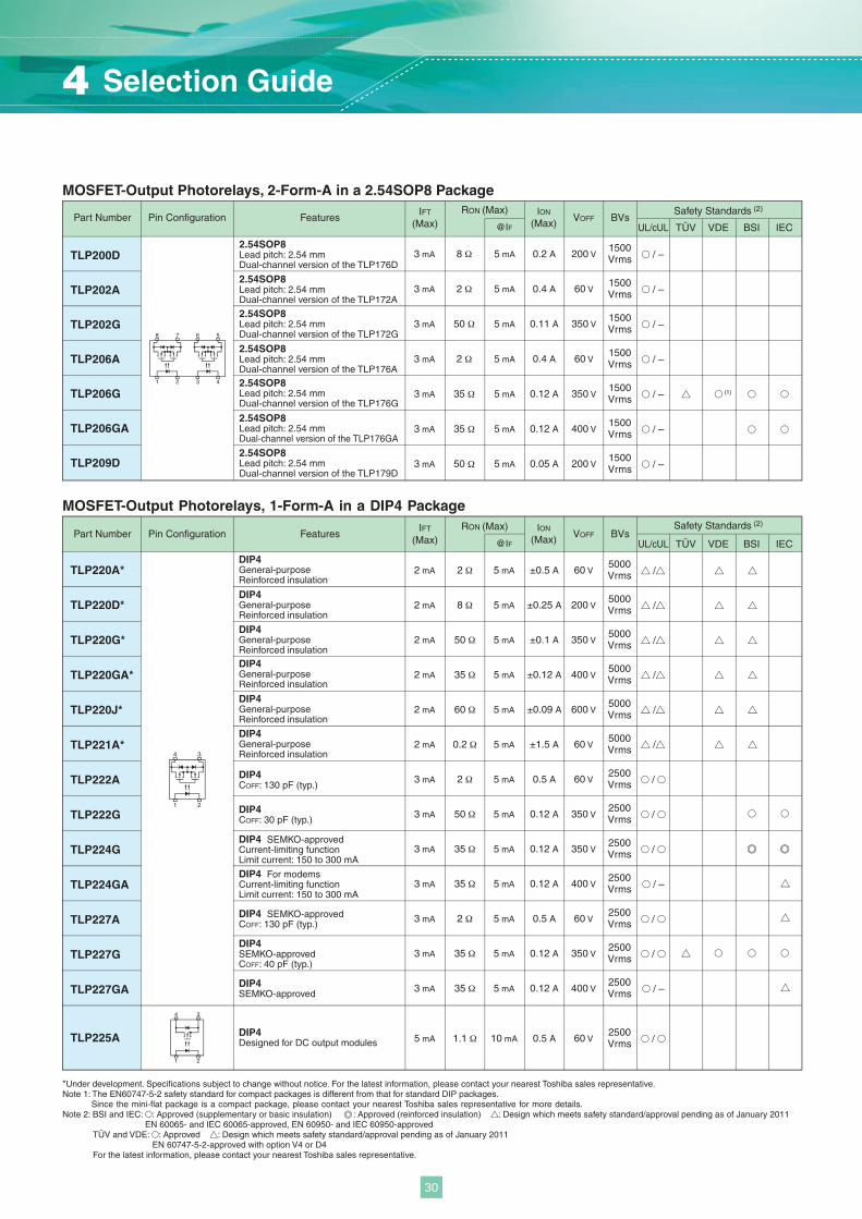
1
4 3
2
4
1
3
2
8
1
6 5
43
7
2
MOSFET-Output Photorelays, 1-Form-A in a DIP4 Package
DIP4COFF: 130 pF (typ.)
2500Vrms /TLP222A 60 V3 mA 2 Ω 5 mA 0.5 A
DIP4 SEMKO-approvedCOFF: 130 pF (typ.) /
2500VrmsTLP227A 60 V3 mA 2 Ω 5 mA 0.5 A
2500Vrms /TLP225A 1.1 Ω5 mA 10 mA 0.5 A
DIP4Designed for DC output modules 60 V
/TLP222G2500Vrms
/2500Vrms350 VTLP224G 35 Ω3 mA 5 mA 0.12 A
DIP4 SEMKO-approvedCurrent-limiting functionLimit current: 150 to 300 mA
350 V50 Ω3 mA 5 mA 0.12 ADIP4COFF: 30 pF (typ.)
/ –2500VrmsTLP224GA 400 V35 Ω3 mA 5 mA 0.12 A
DIP4 For modemsCurrent-limiting functionLimit current: 150 to 300 mA
/ –2500VrmsTLP227GA 400 V35 Ω3 mA 5 mA 0.12 ADIP4
SEMKO-approved
TLP227G /2500Vrms350 V35 Ω3 mA 5 mA 0.12 A
DIP4SEMKO-approvedCOFF: 40 pF (typ.)
5000Vrms /
/
/
/
/
/
TLP220A* 60 V2 mA 2 Ω 5 mA ±0.5 A
5000VrmsTLP220J* 600 V2 mA 60 Ω 5 mA ±0.09 A
TLP220D* 5000Vrms
5000Vrms350 VTLP220G* 50 Ω2 mA 5 mA ±0.1 A
200 V8 Ω2 mA 5 mA ±0.25 A
5000VrmsTLP220GA* 400 V35 Ω2 mA 5 mA ±0.12 A
TLP221A*5000Vrms60 V0.2 Ω2 mA 5 mA ±1.5 A
MOSFET-Output Photorelays, 2-Form-A in a 2.54SOP8 Package
1500VrmsTLP200D / –200 V
2.54SOP8Lead pitch: 2.54 mmDual-channel version of the TLP176D
8 Ω 5 mA3 mA 0.2 A
1500Vrms / –TLP202A 60 V
2.54SOP8Lead pitch: 2.54 mmDual-channel version of the TLP172A
2 Ω 5 mA3 mA 0.4 A
1500VrmsTLP202G / –350 V
2.54SOP8Lead pitch: 2.54 mmDual-channel version of the TLP172G
50 Ω 5 mA3 mA 0.11 A
TLP206A / –1500Vrms60 V
2.54SOP8Lead pitch: 2.54 mmDual-channel version of the TLP176A
2 Ω 5 mA3 mA 0.4 A
1500VrmsTLP206G 350 V
2.54SOP8Lead pitch: 2.54 mmDual-channel version of the TLP176G
35 Ω 5 mA3 mA 0.12 A / – (1)
1500VrmsTLP206GA / –400 V
2.54SOP8Lead pitch: 2.54 mmDual-channel version of the TLP176GA
35 Ω 5 mA3 mA 0.12 A
1500Vrms / –TLP209D 200 V
2.54SOP8Lead pitch: 2.54 mmDual-channel version of the TLP179D
50 Ω 5 mA3 mA 0.05 A
Part Number Pin Configuration FeaturesRON (Max)
VDE BSI IECUL/cUL TÜVBVsVOFF
IFT
(Max) @IF
ION
(Max)Safety Standards (2)
Part Number Pin Configuration FeaturesRON (Max)
VDE BSI IECUL/cUL TÜVBVsVOFF
IFT
(Max) @IF
ION
(Max)Safety Standards (2)
*Under development. Specifications subject to change without notice. For the latest information, please contact your nearest Toshiba sales representative.Note 1: The EN60747-5-2 safety standard for compact packages is different from that for standard DIP packages.
Since the mini-flat package is a compact package, please contact your nearest Toshiba sales representative for more details.Note 2: BSI and IEC: : Approved (supplementary or basic insulation) : Approved (reinforced insulation) : Design which meets safety standard/approval pending as of January 2011
EN 60065- and IEC 60065-approved, EN 60950- and IEC 60950-approvedTÜV and VDE: : Approved : Design which meets safety standard/approval pending as of January 2011
EN 60747-5-2-approved with option V4 or D4For the latest information, please contact your nearest Toshiba sales representative.
DIP4General-purposeReinforced insulation
DIP4General-purposeReinforced insulation
DIP4General-purposeReinforced insulation
DIP4General-purposeReinforced insulation
DIP4General-purposeReinforced insulation
DIP4General-purposeReinforced insulation
4 Selection Guide
30
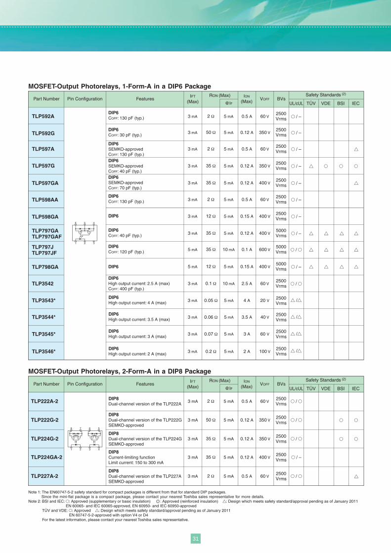
8
1
6 5
43
7
2
6
1
5 4
32
Note 1: The EN60747-5-2 safety standard for compact packages is different from that for standard DIP packages.Since the mini-flat package is a compact package, please contact your nearest Toshiba sales representative for more details.
Note 2: BSI and IEC: : Approved (supplementary or basic insulation) : Approved (reinforced insulation) : Design which meets safety standard/approval pending as of January 2011EN 60065- and IEC 60065-approved, EN 60950- and IEC 60950-approved
TÜV and VDE: : Approved : Design which meets safety standard/approval pending as of January 2011EN 60747-5-2-approved with option V4 or D4
For the latest information, please contact your nearest Toshiba sales representative.
MOSFET-Output Photorelays, 2-Form-A in a DIP8 Package
/TLP222A-2 2500Vrms60 V
DIP8Dual-channel version of the TLP222A
2 Ω 5 mA3 mA 0.5 A
TLP222G-2 2500Vrms /350 V
DIP8Dual-channel version of the TLP222GSEMKO-approved
50 Ω 5 mA3 mA 0.12 A
TLP224G-2 /2500Vrms350 V
DIP8Dual-channel version of the TLP224GSEMKO-approved
35 Ω 5 mA3 mA 0.12 A
/ –TLP224GA-2 2500Vrms400 V
DIP8Current-limiting functionLimit current: 150 to 300 mA
35 Ω 5 mA3 mA 0.12 A
TLP227A-2 /2500Vrms60 V
DIP8Dual-channel version of the TLP227ASEMKO-approved
2 Ω 5 mA3 mA 0.5 A
MOSFET-Output Photorelays, 1-Form-A in a DIP6 Package
DIP6COFF: 130 pF (typ.) / –
2500Vrms
DIP6SEMKO-approvedCOFF: 130 pF (typ.)
/ –TLP597A 2500Vrms60 V3 mA 2 Ω 5 mA 0.5 A
TLP592A 60 V3 mA 2 Ω 5 mA 0.5 A
DIP6COFF: 130 pF (typ.) / –TLP598AA
2500Vrms
DIP6High output current: 2.5 A (max)COFF: 400 pF (typ.)
TLP3542 /2500Vrms60 V3 mA 0.1 Ω 10 mA 2.5 A
60 V3 mA 2 Ω 5 mA 0.5 A
/ –2500Vrms350 VTLP592G 50 Ω3 mA 5 mA 0.12 A
DIP6COFF: 30 pF (typ.)
2500Vrms / –350 V35 Ω3 mA 5 mATLP597G 0.12 A
DIP6SEMKO-approvedCOFF: 40 pF (typ.)
5000Vrms / –400 V35 Ω3 mA 5 mATLP797GA
TLP797GAF0.12 A
DIP6COFF: 40 pF (typ.)
5000Vrms / –400 V12 Ω5 mA 5 mATLP798GA 0.15 ADIP6
5000Vrms /600 V35 Ω5 mA 10 mATLP797J
TLP797JF0.1 A
DIP6COFF: 120 pF (typ.)
DIP6SEMKO-approvedCOFF: 70 pF (typ.)
2500Vrms / –3 mATLP597GA 35 Ω 5 mA 400 V
DIP6 2500Vrms / –3 mATLP598GA 12 Ω 5 mA 400 V0.15 A
0.12 A
Part Number Pin Configuration FeaturesRON (Max)
VDE BSI IECUL/cUL TÜVBVsVOFF
IFT
(Max) @IF
ION
(Max)Safety Standards (2)
Part Number Pin Configuration FeaturesRON (Max)
VDE BSI IECUL/cUL TÜVBVsVOFF
IFT
(Max) @IF
ION
(Max)Safety Standards (2)
2500Vrms
/TLP3543* 20 VDIP6High output current: 4 A (max)
DIP6High output current: 3.5 A (max)
DIP6High output current: 3 A (max)
DIP6High output current: 2 A (max)
0.05 Ω 5 mA3 mA 4 A
2500Vrms
/TLP3544* 40 V0.06 Ω 5 mA3 mA 3.5 A
2500Vrms
/TLP3545* 60 V0.07 Ω 5 mA3 mA 3 A
2500Vrms
/TLP3546* 100 V0.2 Ω 5 mA3 mA 2 A
31
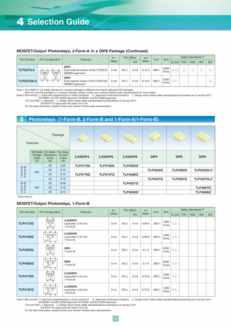
Part Number Pin Configuration FeaturesRON (Max)
VDE BSI IECUL/cUL TÜVBVsVOFF
IFT
(Max) @IF
ION
(Max)Safety Standards (2)
1
4 3
2
6
1
5 4
32
1
4 3
26
1
5 4
32
6
1
5 4
32
1
4 3
2
8
1
6 5
43
7
2
Photorelays (1-Form-B, 2-Form-B and 1-Form-A/1-Form-B)5
MOSFET-Output Photorelays, 1-Form-B
Note 2: BSI and IEC: : Approved (supplementary or basic insulation) : Approved (reinforced insulation) : Design which meets safety standard/approval pending as of January 2011EN 60065- and IEC 60065-approved, EN 60950- and IEC 60950-approved
TÜV and VDE: : Approved : Design which meets safety standard/approval pending as of January 2011EN 60747-5-2-approved with option V4 or D4
For the latest information, please contact your nearest Toshiba sales representative.
2.54SOP4Lead pitch: 2.54 mm1-Form-B
2.54SOP6Lead pitch: 2.54 mm1-Form-B
DIP41-Form-B
DIP61-Form-B
2.54SOP4Lead pitch: 2.54 mm 1-Form-B
2.54SOP6Lead pitch: 2.54 mm 1-Form-B
TLP4197G / –
1500Vrms
1500Vrms
/ –TLP4176G
TLP4592G / –
/ –TLP4222G
2500Vrms
2500Vrms
TLP4192G / –
1500Vrms
1500Vrms
/ –
25 Ω
25 Ω
50 Ω
50 Ω
50 Ω
50 Ω
3 mA
3 mA
3 mA
3 mA
3 mA
3 mA
0 mA
0 mA
0 mA
0 mA
0 mA
0 mATLP4172G
350 V
350 V
350 V
350 V
350 V
350 V
0.12 A
0.12 A
0.1 A
0.1 A
0.09 A
0.09 A
On-StateCurrent(max)
(A)
Off-StateVoltage(max)
(V)
On-StateResistance
(max)(Ω)
Features
Package
0.0950
0.1050350
1-F
orm
-B,
2-F
orm
-B1-
For
m-A
/1-
For
m-B
0.1225
0.1525
0.0950
0.1050350
0.1225
2.54SOP4 2.54SOP6 2.54SOP8 DIP4 DIP6 DIP8
TLP4172G TLP4192G TLP4202G*TLP4222G TLP4592G TLP4222G-2*
TLP4176G TLP4197G TLP4206G*TLP4227G TLP4597G TLP4227G-2*
TLP4027G*TLP4007G*
TLP4026G* TLP4006G** Dual-channel
Part Number Pin Configuration FeaturesRON (Max)
VDE BSI IECUL/cUL TÜVBVsVOFF
IFT
(Max) @IF
ION
(Max)Safety Standards (2)
Note 1: The EN60747-5-2 safety standard for compact packages is different from that for standard DIP packages.Since the mini-flat package is a compact package, please contact your nearest Toshiba sales representative for more details.
Note 2: BSI and IEC: : Approved (supplementary or basic insulation) : Approved (reinforced insulation) : Design which meets safety standard/approval pending as of January 2011EN 60065- and IEC 60065-approved, EN 60950- and IEC 60950-approved
TÜV and VDE: : Approved : Design which meets safety standard/approval pending as of January 2011EN 60747-5-2-approved with option V4 or D4
For the latest information, please contact your nearest Toshiba sales representative.
TLP227G-2 2500Vrms /350 V
DIP8Dual-channel version of the TLP227GSEMKO-approved
35 Ω 5 mA3 mA 0.12 A
DIP8Dual-channel version of the TLP227GASEMKO-approved
TLP227GA-2 2500Vrms / –400 V35 Ω 5 mA3 mA 0.12 A
MOSFET-Output Photorelays, 2-Form-A in a DIP8 Package (Continued)
4 Selection Guide
32
8
1
6 5
43
7
2
8
1
6 5
43
7
2
MOSFET-Output Photorelays, 2-Form-B
MOSFET-Output Photorelays, 1-Form-A/1-Form-B
Note 2: BSI and IEC: : Approved (supplementary or basic insulation) : Approved (reinforced insulation) : Design which meets safety standard/approval pending as of January 2011EN 60065- and IEC 60065-approved, EN 60950- and IEC 60950-approved
TÜV and VDE: : Approved : Design which meets safety standard/approval pending as of January 2011EN 60747-5-2-approved with option V4 or D4
For the latest information, please contact your nearest Toshiba sales representative.
2.54SOP8Lead pitch: 2.54 mmDual-channel version of the TLP4172G2-Form-B
DIP8Dual-channel version of the TLP4222G2-Form-B
2.54SOP8Lead pitch: 2.54 mmDual-channel version of the TLP4176G2-Form-B
DIP8Dual-channel version of the TLP4227G2-Form-BSEMKO-approved
TLP4227G-2 0.15 A25 Ω3 mA2500Vrms / –
1500Vrms / –25 Ω3 mA
TLP4222G-2 0.1 A50 Ω3 mA2500Vrms / –
1500Vrms / –50 Ω
0 mA
0 mA
0 mA
0 mA3 mATLP4202G 350 V
350 V
350 V
350 V
0.09 A
TLP4206G 0.12 A
2.54SOP8Lead pitch: 2.54 1a1b (N.C. + N.O.)
DIP81a1b (N.C. + N.O.)
2.54SOP8Lead pitch: 2.541a1b (N.C. + N.O.)
DIP81a1b (N.C. + N.O.)TLP4006G 0.12 A25 Ω3 mA
2500Vrms / –
1500Vrms / –25 Ω3 mA
TLP4007G 0.1 A50 Ω3 mA2500Vrms / –
1500Vrms / –50 Ω
(Form-A)5 mA
(Form-B)0 mA
(Form-A)5 mA
(Form-B)0 mA
(Form-A)5 mA
(Form-B)0 mA
(Form-A)5 mA
(Form-B)0 mA
3 mATLP4027G 350 V
350 V
350 V
350 V
0.09 A
TLP4026G 0.12 A
Part Number Pin Configuration FeaturesRON (Max)
VDE BSI IECUL/cUL TÜV
VDE BSI IECUL/cUL TÜV
BVsVOFFIFT
(Max) @IF
ION
(Max)
Part Number Pin Configuration FeaturesRON (Max)
BVsVOFFIFT
(Max) @IF
ION
(Max)
Safety Standards (2)
Safety Standards (2)
6
1
5 4
32
1
4 3
2
MOSFET-Output Photorelays, 1-Form-B (Continued)
DIP41-Form-BSEMKO-approved
DIP61-Form-BSEMKO-approved
TLP4597G / –
/ –TLP4227G
2500Vrms
2500Vrms
25 Ω
25 Ω
3 mA
3 mA
0 mA
0 mA 350 V
350 V0.15 A
0.15 A
Part Number Pin Configuration FeaturesRON (Max)
VDE BSI IECUL/cUL TÜVBVsVOFF
IFT
(Max) @IF
ION
(Max)Safety Standards (2)
33
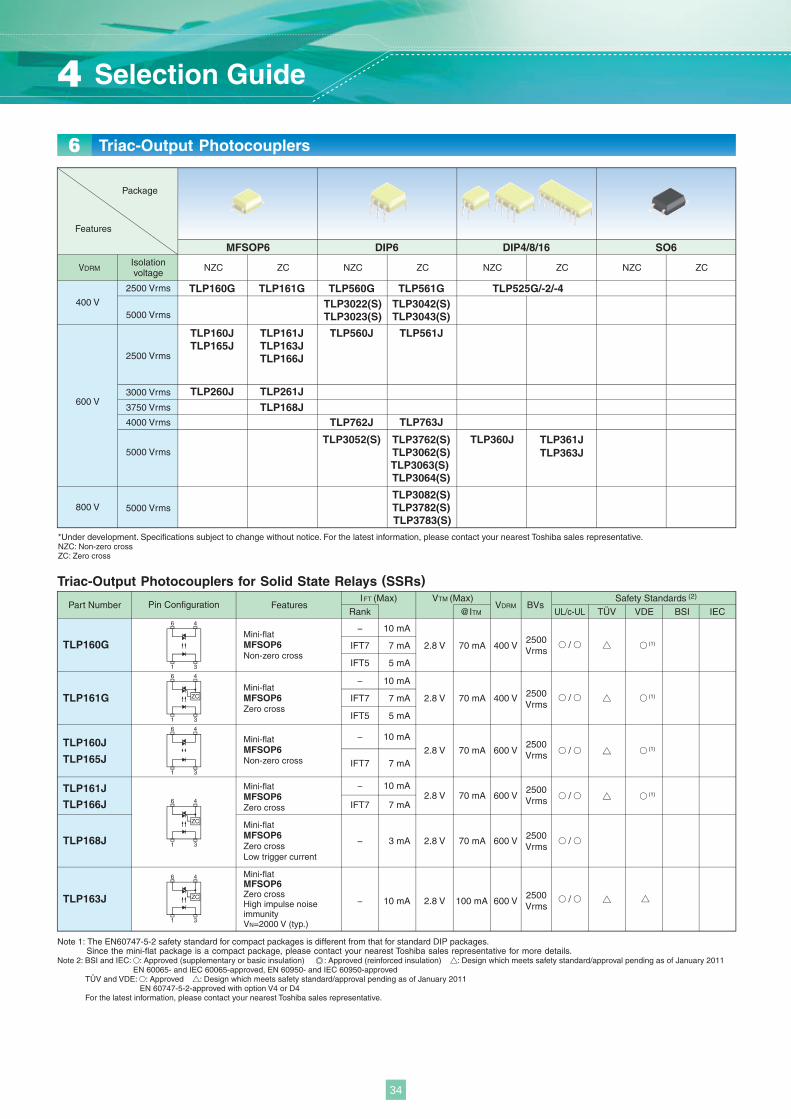
6
1
4
3
6
1
4
3
ZC
6
1
4
3
6
1
4
3
ZC
6
1
4
3
ZC
Triac-Output Photocouplers6
VDRMIsolationvoltage
Features
Package
2500 Vrms
NZC
2500 Vrms
3000 Vrms
3750 Vrms
4000 Vrms
5000 Vrms
5000 Vrms
5000 Vrms
MFSOP6 DIP6 DIP4/8/16 SO6
TLP160G
TLP160JTLP165J
TLP260J
ZC
TLP161G
TLP161JTLP163JTLP166J
TLP261JTLP168J
NZC
TLP560GTLP3022(S)TLP3023(S)
TLP3042(S)TLP3043(S)
TLP3762(S)TLP3062(S)TLP3063(S)TLP3064(S)
TLP3082(S)TLP3782(S) TLP3783(S)
TLP3052(S) TLP361JTLP363J
TLP360J
TLP560J
TLP762J
ZC
TLP561G
TLP561J
TLP763J
NZC
TLP525G/-2/-4
ZC NZC ZC
400 V
600 V
800 V
*Under development. Specifications subject to change without notice. For the latest information, please contact your nearest Toshiba sales representative.NZC: Non-zero crossZC: Zero cross
Note 1: The EN60747-5-2 safety standard for compact packages is different from that for standard DIP packages.Since the mini-flat package is a compact package, please contact your nearest Toshiba sales representative for more details.
Note 2: BSI and IEC: : Approved (supplementary or basic insulation) : Approved (reinforced insulation) : Design which meets safety standard/approval pending as of January 2011EN 60065- and IEC 60065-approved, EN 60950- and IEC 60950-approved
TÜV and VDE: : Approved : Design which meets safety standard/approval pending as of January 2011EN 60747-5-2-approved with option V4 or D4
For the latest information, please contact your nearest Toshiba sales representative.
Triac-Output Photocouplers for Solid State Relays (SSRs)
VDRMPart Number Pin Configuration Features BVsRank VDE BSI IEC
Safety Standards (2)
UL/c-UL TÜV
IFT (Max)
@ITM
VTM (Max)
2500Vrms
2500Vrms
2500Vrms
2500Vrms
2500Vrms
2500Vrms
TLP160J
TLP165J
TLP161J
TLP166J
(1)
(1)
TLP160G
400 V
400 V /
/
/
/
/
/
TLP161G
2.8 V
2.8 V
2.8 V
70 mA
2.8 V 70 mA
70 mA
70 mA
100 mA
(1)
(1)
TLP168J
TLP163J
10 mA
7 mA 2.8 V
2.8 V
5 mA
10 mA
7 mA
5 mA
7 mA
7 mA
10 mA
10 mA
3 mA
10 mA
IFT7
IFT5
IFT7
IFT5
IFT7
IFT7
−
−
−
−
−
−
600 V
600 V
600 V
600 V
Mini-flatMFSOP6Non-zero cross
Mini-flatMFSOP6Zero cross
Mini-flatMFSOP6Non-zero cross
Mini-flatMFSOP6Zero cross
Mini-flatMFSOP6Zero crossLow trigger current
Mini-flatMFSOP6Zero crossHigh impulse noise immunityVN=2000 V (typ.)
70 mA
4 Selection Guide
34
8
1
6 5
43
7
2
16
1
15
2
14
3
13
4
12
5
11
6
10
7
9
8
4
1
3
2
6
1
4
32
4
1
3
2
4
1
3
2
ZC
4
1
3
2
ZC
6
1
4
3
6
1
4
3
ZC
TLP525G-2 10 mA
TLP525G-4 10 mA
−
− /
DIP8Dual-channel version of the TLP525G
DIP164-channel version of the TLP525G
Note 2: BSI and IEC: : Approved (supplementary or basic insulation) : Approved (reinforced insulation) : Design which meets safety standard/approval pending as of January 2011EN 60065- and IEC 60065-approved, EN 60950- and IEC 60950-approved
TÜV and VDE: : Approved : Design which meets safety standard/approval pending as of January 2011EN 60747-5-2-approved with option V4 or D4
For the latest information, please contact your nearest Toshiba sales representative.
Triac-Output Photocouplers for AC 100 to 120 V Lines
VDE BSI IECTÜV@ITM
10 mA
IFT7 7 mA
IFT5 5 mA
TLP525G
TLP560G
10 mA /2500Vrms
/ –
−
−
VDRMPart Number Pin Configuration Features BVsRank
Safety Standards (2)IFT (Max) VTM (Max)
UL/c-UL
DIP4
DIP6General-purposeNon-zero cross
100 mA 400 V3 V
2500Vrms
100 mA 400 V3 V
/2500Vrms
100 mA 400 V3 V
2500Vrms
100 mA 400 V3 V
Triac-Output Photocouplers for Office Equipment
VDRMPart Number Pin Configuration Features BVsRank
Safety Standards (2)IFT (Max) VTM (Max)
VDE BSI IECUL/c-UL TÜV@ITM
TLP360JTLP360JF
7 mA
TLP363JTLP363JF
10 mA
7 mA
10 mA
/
IFT7
−
10 mA /−
IFT7
−TLP361JTLP361JF
5000Vrms70 mA2.8 V /600 V
5000Vrms70 mA2.8 V 600 V
5000Vrms70 mA2.8 V 600 V
DIP4Non-zero cross
DIP4Zero cross
DIP4Zero crossHigh impulse noise immunityVN = 2000 V (typ.)
Triac-Output Photocouplers for Solid State Relays (SSRs) (Continued)
VDRMPart Number Pin Configuration Features BVsRank VDE BSI IEC
Safety Standards (2)
UL/c-UL TÜV
IFT (Max)
@ITM
VTM (Max)
(1)/ –
/ –
70 mA
70 mA
TLP260J
3000Vrms
3000Vrms
(1)TLP261J
10 mA
10 mA
−
− 600 V
600 VMini-flatMFSOP6Non-zero cross
Mini-flatMFSOP6Zero cross
2.8 V
2.8 V
35
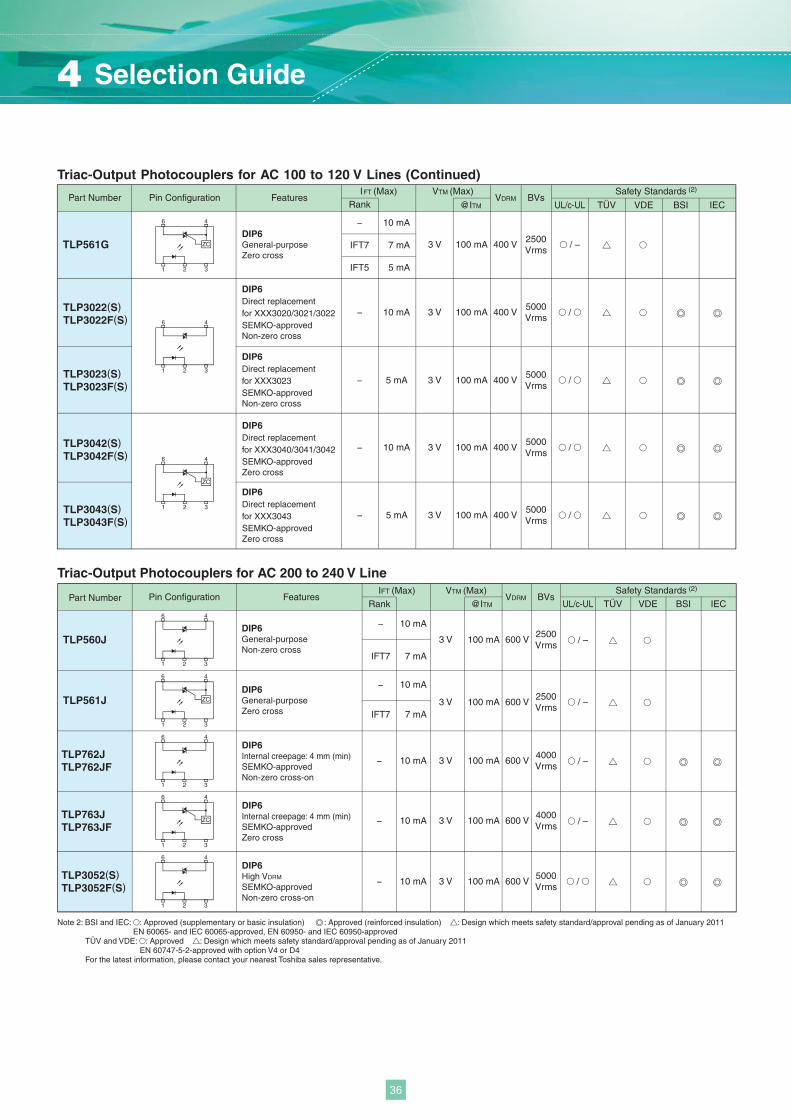
6
1
4
32
ZC
6
1
4
32
6
1
4
32
ZC
6
1
4
32
6
1
4
32
ZC
6
1
4
32
6
1
4
32
ZC
6
1
4
32
Triac-Output Photocouplers for AC 200 to 240 V Line
Note 2: BSI and IEC: : Approved (supplementary or basic insulation) : Approved (reinforced insulation) : Design which meets safety standard/approval pending as of January 2011EN 60065- and IEC 60065-approved, EN 60950- and IEC 60950-approved
TÜV and VDE: : Approved : Design which meets safety standard/approval pending as of January 2011EN 60747-5-2-approved with option V4 or D4
For the latest information, please contact your nearest Toshiba sales representative.
Part Number Pin Configuration Features BVsVDRMRank VDE BSI IEC
Safety Standards (2)
UL/c-UL TÜV
IFT (Max)
@ITM
VTM (Max)
DIP6Internal creepage: 4 mm (min)SEMKO-approvedNon-zero cross-on
DIP6Internal creepage: 4 mm (min)SEMKO-approvedZero cross
DIP6High VDRM
SEMKO-approvedNon-zero cross-on
TLP762JTLP762JF
TLP763JTLP763JF
TLP3052(S)TLP3052F(S)
10 mA
10 mA
10 mA
−
−
−
/ –
/ –
/
4000Vrms
4000Vrms
5000Vrms
10 mA
IFT7 7 mA
IFT5 5 mA
TLP561G
−
IFT7 7 mA
IFT7 7 mA
TLP560J
10 mA
TLP561J
10 mA
−
−
/ –3 V 600 V
/ –
2500Vrms
100 mA
3 V 600 V100 mA
3 V 600 V100 mA
3 V 600 V100 mA
3 V 600 V2500Vrms
100 mA
DIP6General-purposeZero cross
DIP6General-purposeNon-zero cross
DIP6General-purposeZero cross
DIP6Direct replacementfor XXX3020/3021/3022SEMKO-approvedNon-zero cross
DIP6Direct replacementfor XXX3023SEMKO-approvedNon-zero cross
−
−
10 mA
5 mA
/
/ –
5000Vrms
100 mA 400 V3 V
5000Vrms
2500Vrms
100 mA 400 V3 V
100 mA 400 V3 V
100 mA 400 V3 V
/
TLP3022(S)TLP3022F(S)
TLP3023(S)TLP3023F(S)
Triac-Output Photocouplers for AC 100 to 120 V Lines (Continued)
VDE BSI IECTÜV@ITMVDRMPart Number Pin Configuration Features BVs
RankSafety Standards (2)IFT (Max) VTM (Max)
UL/c-UL
DIP6Direct replacementfor XXX3040/3041/3042SEMKO-approvedZero cross
−
−
10 mA
5 mA
5000Vrms
/
100 mA 400 V3 V5000Vrms
/
TLP3042(S)TLP3042F(S)
TLP3043(S)TLP3043F(S)
DIP6Direct replacementfor XXX3043SEMKO-approvedZero cross
4 Selection Guide
36
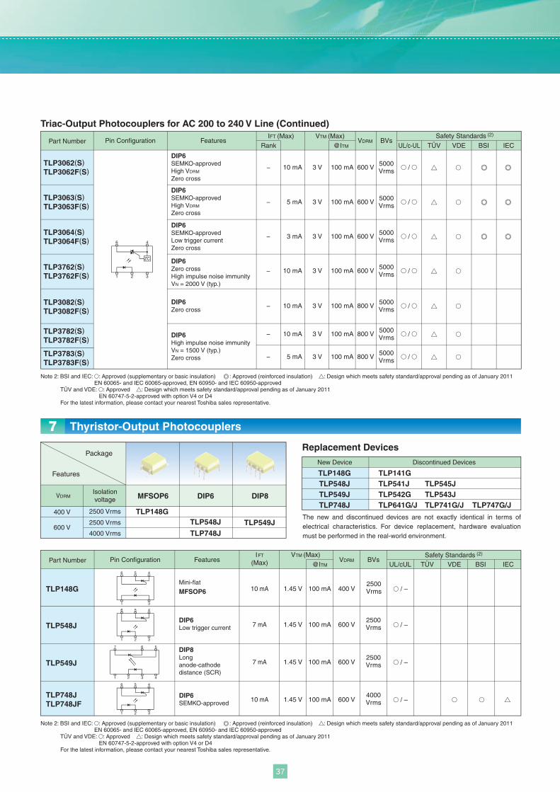
6
1
5 4
3
6
1
5 4
32
2
6 5
41 3
7
6
1
5 4
32
ZC
6
1
4
32
Part Number Pin Configuration Features VDRM BVsVDE BSI IEC
Safety Standards (2)
UL/cUL TÜV
IFT
(Max) @ITM
VTM (Max)
TLP148GMini-flat
MFSOP6 1.45 V 400 V100 mA10 mA2500Vrms
TLP548JDIP6Low trigger current
2500Vrms1.45 V7 mA 100 mA 600 V
TLP549J
DIP8Longanode-cathodedistance (SCR)
2500Vrms1.45 V7 mA 100 mA 600 V
TLP748JTLP748JF
DIP6SEMKO-approved
4000Vrms1.45 V10 mA 100 mA 600 V
Note 2: BSI and IEC: : Approved (supplementary or basic insulation) : Approved (reinforced insulation) : Design which meets safety standard/approval pending as of January 2011EN 60065- and IEC 60065-approved, EN 60950- and IEC 60950-approved
TÜV and VDE: : Approved : Design which meets safety standard/approval pending as of January 2011EN 60747-5-2-approved with option V4 or D4
For the latest information, please contact your nearest Toshiba sales representative.
/ –
/ –
/ –
/ –
Replacement Devices
VDRMIsolationvoltage
Features
New DevicePackage
2500 Vrms
2500 Vrms
4000 Vrms
MFSOP6 DIP8DIP6
TLP148G
TLP148GTLP548JTLP549JTLP748J
Discontinued Devices
TLP141GTLP541JTLP542GTLP641G/J
TLP545JTLP543JTLP741G/J TLP747G/J
TLP548J
TLP748JTLP549J
400 V
600 V
The new and discontinued devices are not exactly identical in terms of electrical characteristics. For device replacement, hardware evaluation must be performed in the real-world environment.
Thyristor-Output Photocouplers7
Triac-Output Photocouplers for AC 200 to 240 V Line (Continued)
Note 2: BSI and IEC: : Approved (supplementary or basic insulation) : Approved (reinforced insulation) : Design which meets safety standard/approval pending as of January 2011EN 60065- and IEC 60065-approved, EN 60950- and IEC 60950-approved
TÜV and VDE: : Approved : Design which meets safety standard/approval pending as of January 2011EN 60747-5-2-approved with option V4 or D4
For the latest information, please contact your nearest Toshiba sales representative.
Part Number Pin Configuration Features BVsVDRMRank VDE BSI IEC
Safety Standards (2)
UL/c-UL TÜV
IFT (Max)
@ITM
VTM (Max)
DIP6SEMKO-approvedHigh VDRM
Zero cross
DIP6SEMKO-approvedHigh VDRM
Zero cross
DIP6SEMKO-approvedLow trigger currentZero cross
DIP6High impulse noise immunityVN = 1500 V (typ.)Zero cross
DIP6Zero crossHigh impulse noise immunityVN = 2000 V (typ.)
DIP6Zero cross
TLP3062(S)TLP3062F(S)
TLP3063(S)TLP3063F(S)
TLP3064(S)TLP3064F(S)
TLP3082(S)TLP3082F(S)
TLP3762(S)TLP3762F(S)
TLP3782(S)TLP3782F(S)
TLP3783(S)TLP3783F(S)
3 V
10 mA
5 mA
3 mA
−
−
−
600 V
600 V
600 V
/
5000Vrms
5000Vrms
5000Vrms
5000Vrms
5000Vrms
5000Vrms
100 mA
3 V 100 mA
3 V 100 mA
600 V 5000Vrms3 V 100 mA
3 V 100 mA
3 V 100 mA
3 V 100 mA
10 mA−
10 mA−
800 V
800 V
800 V
10 mA−
/
/
5 mA−
/
/
/
/
37
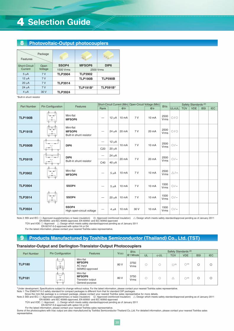
6
1
4
3
6
1
4
3
6
1
4
32
6
1
4
32
6
1
4
3
4
1
3
2
6
1
4
3
4
1
6
3
Photovoltaic-Output photocouplers8
VDE BSI IECUL/cUL TÜV@IF@IF
2500Vrms
2500Vrms
2500Vrms
2500Vrms
2500Vrms
1500Vrms
1500Vrms
1500Vrms
— 12 μA
C20 20 μA
— 24 μA
C40 40 μA
TLP190B — 12 μA
5 μA
10 mA 7 V 10 mA
TLP191B — 24 μA
— 5 μA
20 mA 7 V 20 mA
TLP590B 10 mA 7 V 10 mA
TLP591B
TLP3904
TLP3914
TLP3924
20 mA 7 V 20 mA
Mini-flatMFSOP6
Mini-flatMFSOP6Built-in shunt resistor
Mini-flatMFSOP6
DIP6
10 mA 7 V 10 mA
— 20 μA 10 mA 7 V 10 mA
— 4 μA 10 mA 30 V 10 mA
— 5 μATLP3902 10 mA 7 V 10 mA
/
/
/ –
/ –
/ –
/ –
/ –
/ –
SSOP4High open-circuit voltage
DIP6Built-in shunt resistor
Part Number Pin Configuration Features BVsRank
Safety Standards (2)Short-Circuit Current (Min) Open-Circuit Voltage (Min)
Note 2: BSI and IEC: : Approved (supplementary or basic insulation) : Approved (reinforced insulation) : Design which meets safety standard/approval pending as of January 2011EN 60065- and IEC 60065-approved, EN 60950- and IEC 60950-approved
TÜV and VDE: : Approved : Design which meets safety standard/approval pending as of January 2011EN 60747-5-2-approved with option V4 or D4
For the latest information, please contact your nearest Toshiba sales representative.
SSOP4
SSOP4
*Built-in shunt resistor
OpenVoltage
Short-CircuitCurrent
Features
Package
1500 Vrms 2500 Vrms
SSOP4 DIP6MFSOP6
TLP3904
TLP3914
TLP3924
TLP3902
TLP190B TLP590B
TLP191B* TLP591B*
7 V
12 μA 7 V
20 μA 7 V
24 μA 7 V
4 μA 30 V
(1)
TLP181 (1)
TLP180 3750Vrms
80 V
3750Vrms
80 V
(1)
Mini-flatMFSOP6AC input SEMKO-approved
Mini-flatMFSOP6Transistor outputGeneral-purpose
Products Manufactured by Toshiba Semiconductor (Thailand) Co., Ltd. (TST) 9
VCEOVDE BSI IECUL TÜVc-UL
Part Number Pin Configuration FeaturesBVs
@1 MinuteSafety Standards (2)
*Under development. Specifications subject to change without notice. For the latest information, please contact your nearest Toshiba sales representative.Note 1: The EN60747-5-2 safety standard for compact packages is different from that for standard DIP packages.
Since the mini-flat package is a compact package, please contact your nearest Toshiba sales representative for more details.Note 2: BSI and IEC: : Approved (supplementary or basic insulation) : Approved (reinforced insulation) : Design which meets safety standard/approval pending as of January 2011
EN 60065- and IEC 60065-approved, EN 60950- and IEC 60950-approvedTÜV and VDE: : Approved : Design which meets safety standard/approval pending as of January 2011
EN 60747-5-2-approved with option V4 or D4For the latest information, please contact your nearest Toshiba sales representative.
Some of the photocouplers with triac output are also manufactured by Toshiba Semiconductor Thailand Co.,Ltd. For detailed information, please contact your nearest Toshiba sales representative.
Transistor-Output and Darlington-Transistor-Output Photocouplers
4 Selection Guide
38
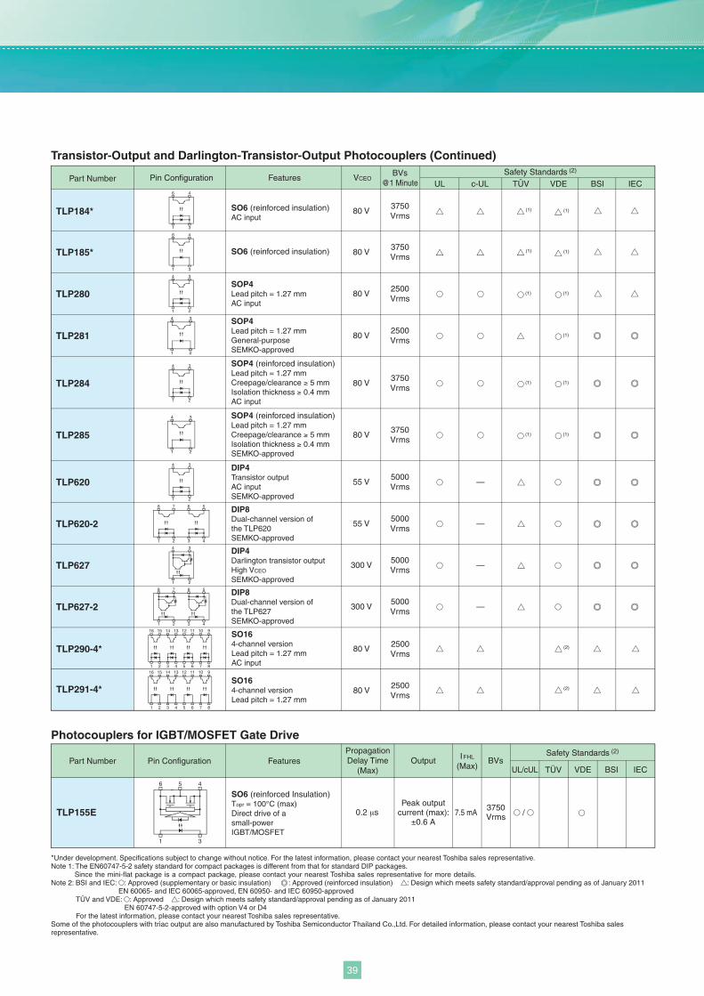
4
1
3
2
4
1
3
2
4
1
3
2
8
1
6 5
43
7
2
4
1
3
2
8
1
6 5
43
7
2
4
1
6
3
16
1
15
2
14
3
13
4
12
5
11
6
10
7
9
816
1
15
2
14
3
13
4
12
5
11
6
10
7
9
8
6
1
5 4
3
6
1
4
3
4
1
3
2
4
1
3
2
VCEOVDE BSI IECUL TÜV
TLP627 300 V
TLP627-2
5000Vrms
300 V5000Vrms
5000Vrms
5000Vrms
TLP620
55 V
55 V
TLP620-2
2500Vrms
2500Vrms
TLP185*
TLP281
TLP280
TLP284
TLP2853750Vrms
3750Vrms
80 V
80 V
80 V
80 V
3750Vrms
80 V
c-ULPart Number Pin Configuration Features
BVs@1 Minute
Safety Standards (2)
(1)
(1)
(1)(1)
(1)(1)
—
—
—
—
(1)
(1)(1)
DIP4Transistor outputAC input SEMKO-approved
DIP8Dual-channel version of the TLP620SEMKO-approved
DIP4Darlington transistor outputHigh VCEO
SEMKO-approved
DIP8Dual-channel version of the TLP627SEMKO-approved
SOP4Lead pitch = 1.27 mmGeneral-purposeSEMKO-approved
SOP4Lead pitch = 1.27 mmAC input
SOP4 (reinforced insulation)Lead pitch = 1.27 mmCreepage/clearance ≥ 5 mmIsolation thickness ≥ 0.4 mmAC input
SOP4 (reinforced insulation)Lead pitch = 1.27 mmCreepage/clearance ≥ 5 mmIsolation thickness ≥ 0.4 mmSEMKO-approved
SO6 (reinforced insulation)
TLP184*3750Vrms
80 V (1)(1)SO6 (reinforced insulation)AC input
TLP290-4*
TLP291-4*
2500Vrms
2500Vrms
80 V
80 V
(2)
(2)
SO164-channel versionLead pitch = 1.27 mmAC input
SO164-channel versionLead pitch = 1.27 mm
*Under development. Specifications subject to change without notice. For the latest information, please contact your nearest Toshiba sales representative.Note 1: The EN60747-5-2 safety standard for compact packages is different from that for standard DIP packages.
Since the mini-flat package is a compact package, please contact your nearest Toshiba sales representative for more details.Note 2: BSI and IEC: : Approved (supplementary or basic insulation) : Approved (reinforced insulation) : Design which meets safety standard/approval pending as of January 2011
EN 60065- and IEC 60065-approved, EN 60950- and IEC 60950-approvedTÜV and VDE: : Approved : Design which meets safety standard/approval pending as of January 2011
EN 60747-5-2-approved with option V4 or D4For the latest information, please contact your nearest Toshiba sales representative.
Some of the photocouplers with triac output are also manufactured by Toshiba Semiconductor Thailand Co.,Ltd. For detailed information, please contact your nearest Toshiba sales representative.
Transistor-Output and Darlington-Transistor-Output Photocouplers (Continued)
TLP155E 3750Vrms0.2 μs
Peak outputcurrent (max):
±0.6 A7.5 mA /
SO6 (reinforced Insulation)Topr = 100°C (max)Direct drive of a small-power IGBT/MOSFET
Photocouplers for IGBT/MOSFET Gate Drive
OutputVDE BSI IECUL/cUL TÜV
Part Number Pin Configuration Features BVsSafety Standards (2)Propagation
Delay Time(Max)
IFHL
(Max)
39
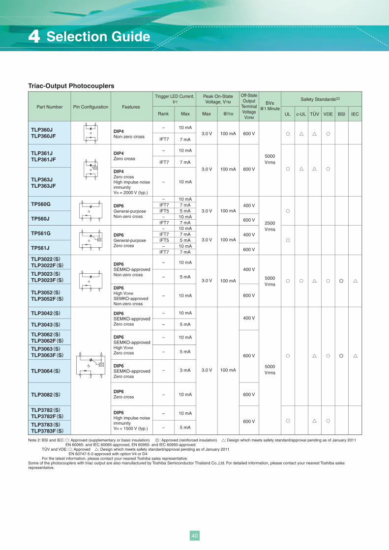
ZC
6
1
4
32
6
1
4
32
ZC
6
1
4
32
4
1
3
2
4
1
3
2
ZC
6
1
4
32
Triac-Output Photocouplers
TLP3042 (S)
TLP3043 (S)
TLP3062 (S)TLP3062F (S)
TLP3063 (S)TLP3063F (S)
TLP3064 (S)
TLP3082 (S)
TLP3782 (S)TLP3782F (S)
TLP3783 (S)TLP3783F (S)
TLP360JTLP360JF
TP560G
TLP361JTLP361JF
TLP363JTLP363JF
TLP3022 (S)TLP3022F (S)
TLP3023 (S)TLP3023F (S)
TLP3052 (S)TLP3052F (S)
TP560J
TP561G
TP561J
DIP4Non-zero cross
DIP6General-purposeNon-zero cross
DIP6General-purposeZero cross
DIP6SEMKO-approvedNon-zero cross
DIP6High VDRM
SEMKO-approvedNon-zero cross
DIP4Zero cross
DIP4Zero crossHigh impulse noise immunityVN = 2000 V (typ.)
DIP6SEMKO-approvedZero cross
DIP6SEMKO-approvedZero cross
DIP6Zero cross
DIP6High impulse noise immunityVN = 1500 V (typ.)
DIP6SEMKO-approvedHigh VDRM
Zero cross
100 mA
100 mA
100 mA
100 mA
100 mA
100 mA
5000Vrms
5000Vrms
5000Vrms
2500Vrms
10 mA
7 mA
7 mA
10 mA
7 mA
7 mA
5 mA
10 mA
5 mA
10 mA
5 mA
10 mA
10 mA
10 mA
5 mA
5 mA
3 mA
10 mA
10 mA
10 mA
7 mA
7 mA
5 mA
10 mA
10 mA
10 mA
–
IFT7
IFT7
–
IFT7
IFT7
IFT5
–
–
–
–
–
–
–
–
–
–
–
–
–
IFT7
IFT7
IFT5
–
–
–
3.0 V
3.0 V
3.0 V
3.0 V
3.0 V
3.0 V
600 V
600 V
400 V
600 V
400 V
600 V
Off-StateOutput
TerminalVoltageVDRM
BVs@1 Minute
Rank Max VDE BSI IECTÜV@ITMMax UL c-UL
Part Number Pin Configuration Features
Safety Standards(2)Tingger LED Current, IFT
Peak On-StateVoltage, VTM
Note 2: BSI and IEC: : Approved (supplementary or basic insulation) : Approved (reinforced insulation) : Design which meets safety standard/approval pending as of January 2011EN 60065- and IEC 60065-approved, EN 60950- and IEC 60950-approved
TÜV and VDE: : Approved : Design which meets safety standard/approval pending as of January 2011EN 60747-5-2-approved with option V4 or D4
For the latest information, please contact your nearest Toshiba sales representative.Some of the photocouplers with triac output are also manufactured by Toshiba Semiconductor Thailand Co.,Ltd. For detailed information, please contact your nearest Toshiba sales representative.
400 V
600 V
400 V
600 V
600 V
600 V
4 Selection Guide
40
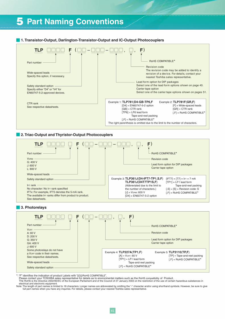
1. Transistor-Output, Darlington-Transistor-Output and IC-Output Photocouplers
TLP F F )( , ,– –
Part number
Wide-spaced leadsSpecify this option, if necessary.
Safety standard optionSpecify either “D4” or “V4” for EN60747-5-2-approved devices.
CTR rankSee respective datasheets.
RoHS COMPATIBLE*
Revision codeThe revision code may be added to identify a revision of a device. For details, contact your nearest Toshiba sales representative.
Lead form option for DIP packagesSelect one of the lead form options shown on page 40.Carrier tape optionSelect one of the carrier tape options shown on pages 51.
Example 1: TLP781(D4-GB-TP6,F[D4] = EN60747-5-2 option[GB] = CTR rank[TP6] = LF6 lead form
Tape-and-reel packing[,F] = RoHS COMPATIBLE*
The right parenthesis is omitted due to the limit to the number of characters.
Example 2: TLP781F(GR,F)[F] = Wide-spaced leads[GR] = CTR rank[,F] = RoHS COMPATIBLE*
2. Triac-Output and Thyristor-Output Photocouplers
F F )( , ,– –TLP
Part number
VDRM
G: 400 VJ: 600 VL: 800 V
Wide-spaced leads
Safety standard option
IFT rankNo character: No IFT rank specifiedIFTx: For example, IFT5 denotes the 5-mA rank.The available IFT ranks differ from product to product. See datasheets.
RoHS COMPATIBLE*
Revision code
Lead form option for DIP packagesCarrier tape option
Example 3: TLP361J(D4-IFT7-TP1,S,F)TLP361J(D4T7TP1S,F)(Abbreviated due to the limit to the number of characters.)[J] = VDRM: 600 V[D4] = EN60747-5-2 option
[IFT7] = [T7] = IFT = 7 mA[TP1] = LF1 lead form
Tape-and-reel packing[,S] = [S] = Revision code: S[,F] = RoHS COMPATIBLE*
3. Photorelays
Example 5: TLP3110(TP,F)[TP] = Tape-and-reel packing[,F] = RoHS COMPATIBLE*
F ( –TLP
Part number
VOFF
A: 60 VD: 200 VG: 350 VGA: 400 VJ: 600 VSome photorelays do not have a VOFF code in their names. See respective datasheets.
Wide-spaced leads
Safety standard option
F ), ,
RoHS COMPATIBLE*
Revision code
Lead form option for DIP packagesCarrier tape option
Example 4: TLP227A(TP1,F)[A] = VOFF: 60 V[TP1] = LF1 lead form
Tape-and-reel packing[,F] = RoHS COMPATIBLE*
*: “F” identifies the indication of product Labels with “[[G]]/RoHS COMPATIBLE”.Please contact your TOSHIBA sales representative for details as to environmental matters such as the RoHS compatibility of Product.The RoHS is the Directive 2002/95/EC of the European Parliament and of the Council of 27 January 2003 on the restriction of the use of certain hazardous substances in electrical and electronic equipment.
Note: The length of part names is limited to 18 characters. Longer names are abbreviated by omitting the “-“ character and/or using shorthand symbols. However, be sure to give full part names when you have any inquiries. For details, please contact your nearest Toshiba sales representative.
5 Part Naming Conventions
41
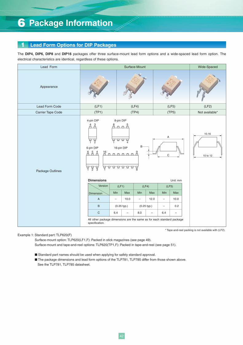
4 3
1 2
4-pin DIP
6 45
1 2 3
6-pin DIP16
1
9
8
16-pin DIP
8 5
1 4
8-pin DIP
A
B
C
10.16
10 to 12
Lead Form Options for DIP Packages1
Lead Form
Lead Form Code
Carrier Tape Code
Appearance
Package Outlines
* Tape-and-reel packing is not available with (LF2).
(LF1) (LF4) (LF5) (LF2)
(TP1) (TP4) (TP5) Not available*
The DIP4, DIP6, DIP8 and DIP16 packages offer three surface-mount lead form options and a wide-spaced lead form option. The
electrical characteristics are identical, regardless of these options.
Example 1: Standard part: TLP620(F)
Surface-mount option: TLP620(LF1,F): Packed in stick magazines (see page 49).
Surface-mount and tape-and-reel options: TLP620(TP1,F): Packed in tape-and-reel (see page 51).
■ Standard part names should be used when applying for safety standard approval.
■ The package dimensions and lead form options of the TLP781, TLP785 differ from those shown above.
See the TLP781, TLP785 datasheet.
All other package dimensions are the same as for each standard package specification.
Unit: mmDimensions
Version (LF1) (LF4) (LF5)
Dimension
–
–
6.4
12.0
–
–
8.0
(0.25 typ.)
10.0
–
(0.35 typ.)
–
6.4
10.0
0.2
–
A
B
C
Min Max Min Min MaxMax
Surface-Mount Wide-Spaced
6 Package Information
42
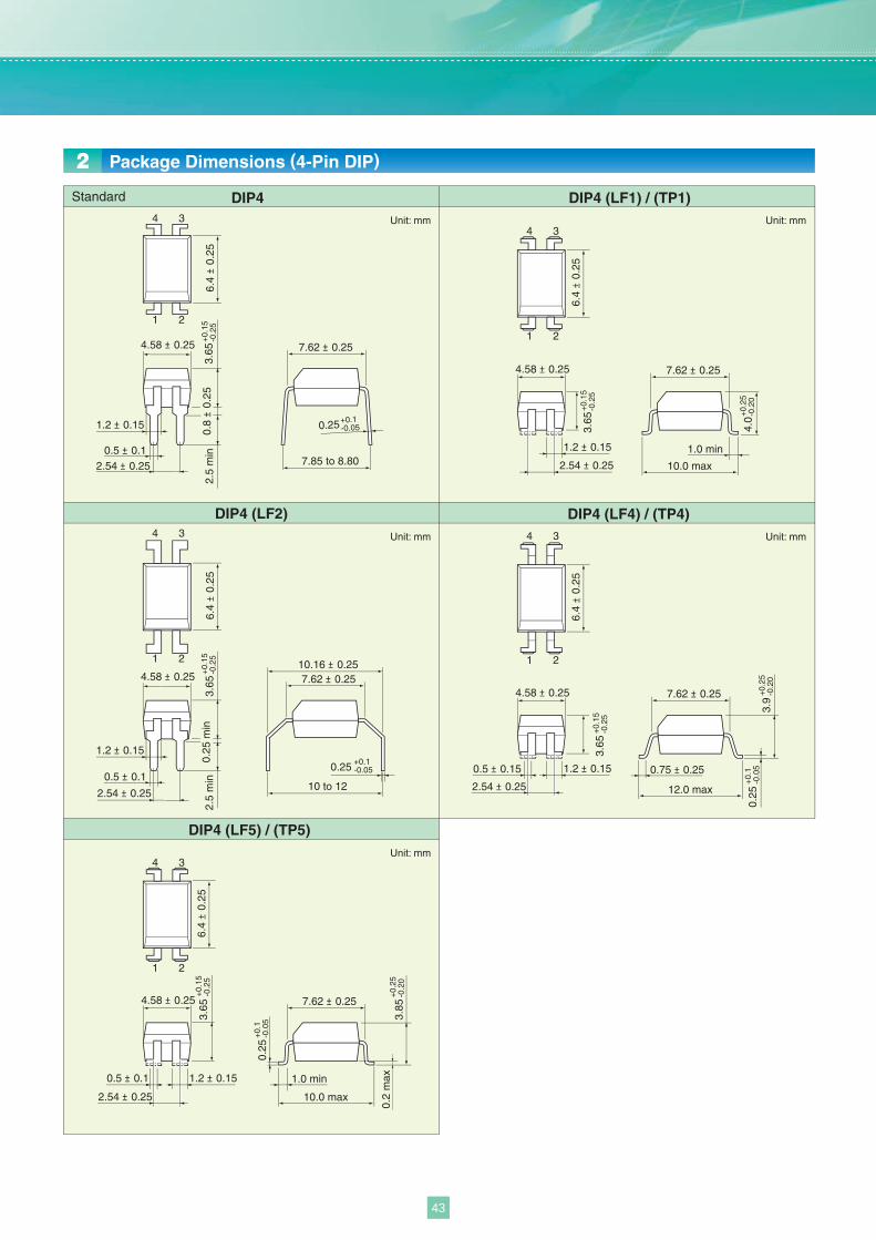
4 3
1 2
6.4
± 0.
25
7.85 to 8.80
7.62 ± 0.25
0.25+0.1-0.05
3.65
+0.
15-0
.25
1.2 ± 0.15
0.5 ± 0.12.54 ± 0.25
4.58 ± 0.25
0.8
±0.
252.
5 m
in
4 3
1 2
6.4
± 0.
25
10.0 max
1.0 min
7.62 ± 0.25
3.65
+0.
15-0
.25
4.58 ± 0.25
2.54 ± 0.25
1.2 ± 0.15
4.0
+0.
25-0
.20
12.0 max
0.75 ± 0.25
7.62 ± 0.25
3.65
+0.
15-0
.25
4.58 ± 0.25
2.54 ± 0.25
1.2 ± 0.15
0.25
+0.
1-0
.05
3.9
+0.
25-0
.20
4 3
1 2
6.4
± 0.
25
0.5 ± 0.15
4 3
1 2
6.4
± 0.
25
10 to 12
0.25
7.62 ± 0.25
3.65
+0.
15-0
.25
1.2 ± 0.15
0.5 ± 0.1
2.54 ± 0.25
4.58 ± 0.25
0.25
min
2.5
min
10.16 ± 0.25
+0.1-0.05
4 3
1 2
6.4
± 0.
25
10.0 max
1.0 min
7.62 ± 0.25
3.65
+0.
15-0
.25
0.25
+0.
1-0
.05
4.58 ± 0.25
2.54 ± 0.25
1.2 ± 0.15
3.85
+0.
25-0
.20
0.2
max0.5 ± 0.1
Package Dimensions (4-Pin DIP)2Standard DIP4
DIP4 (LF2) DIP4 (LF4) / (TP4)
DIP4 (LF5) / (TP5)
Unit: mmUnit: mm
Unit: mmUnit: mm
Unit: mm
DIP4 (LF1) / (TP1)
43
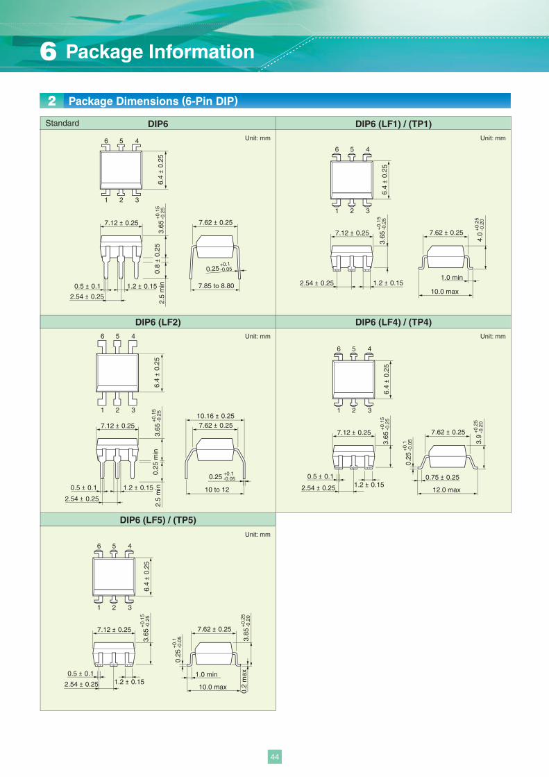
6 5 4
1 2 3
7.12 ± 0.25
6.4
±0.
25
1.2 ± 0.152.54 ± 0.25
3.65 7.62 ± 0.25
10.0 max
1.0 min
+0.
15-0
.25
4.0
+0.
25-0
.20
6 5 4
1 2 3
7.12 ± 0.25
6.4
±0.
25
0.5 ± 0.1 1.2 ± 0.15
2.54 ± 0.25
2.5
min
0.25
min
3.65 7.62 ± 0.25
10.16 ± 0.25
10 to 12
+0.
15-0
.25
0.25 +0.1-0.05
6 5 4
1 2 3
7.12 ± 0.25
6.4
±0.
25
1.2 ± 0.150.5 ± 0.1
2.54 ± 0.25
3.65
7.62 ± 0.25
12.0 max
0.75 ± 0.25
+0.
15-0
.25
0.25
+0.
1-0
.05 3.9
+0.
25-0
.20
6 5 4
1 2 3
7.12 ± 0.25
6.4
±0.
25
1.2 ± 0.150.5 ± 0.1
2.54 ± 0.25
3.65
7.62 ± 0.25
10.0 max
1.0 min
+0.
15-0
.25
0.25
+0.
1-0
.05 3.85
0.2
max
+0.
25-0
.20
6 5 4
1 2 3
7.12 ± 0.25
6.4
±0.
25
0.5 ± 0.1 1.2 ± 0.15
2.54 ± 0.25
2.5
min
0.8
±0.
253.
65 7.62 ± 0.25
0.25+0.1-0.05
7.85 to 8.80
+0.
15-0
.25
DIP6 (LF4) / (TP4)
DIP6 (LF5) / (TP5)
DIP6 (LF1) / (TP1)
DIP6 (LF2)
DIP6Standard
Package Dimensions (6-Pin DIP)
Unit: mmUnit: mm
Unit: mmUnit: mm
Unit: mm
2
6 Package Information
44
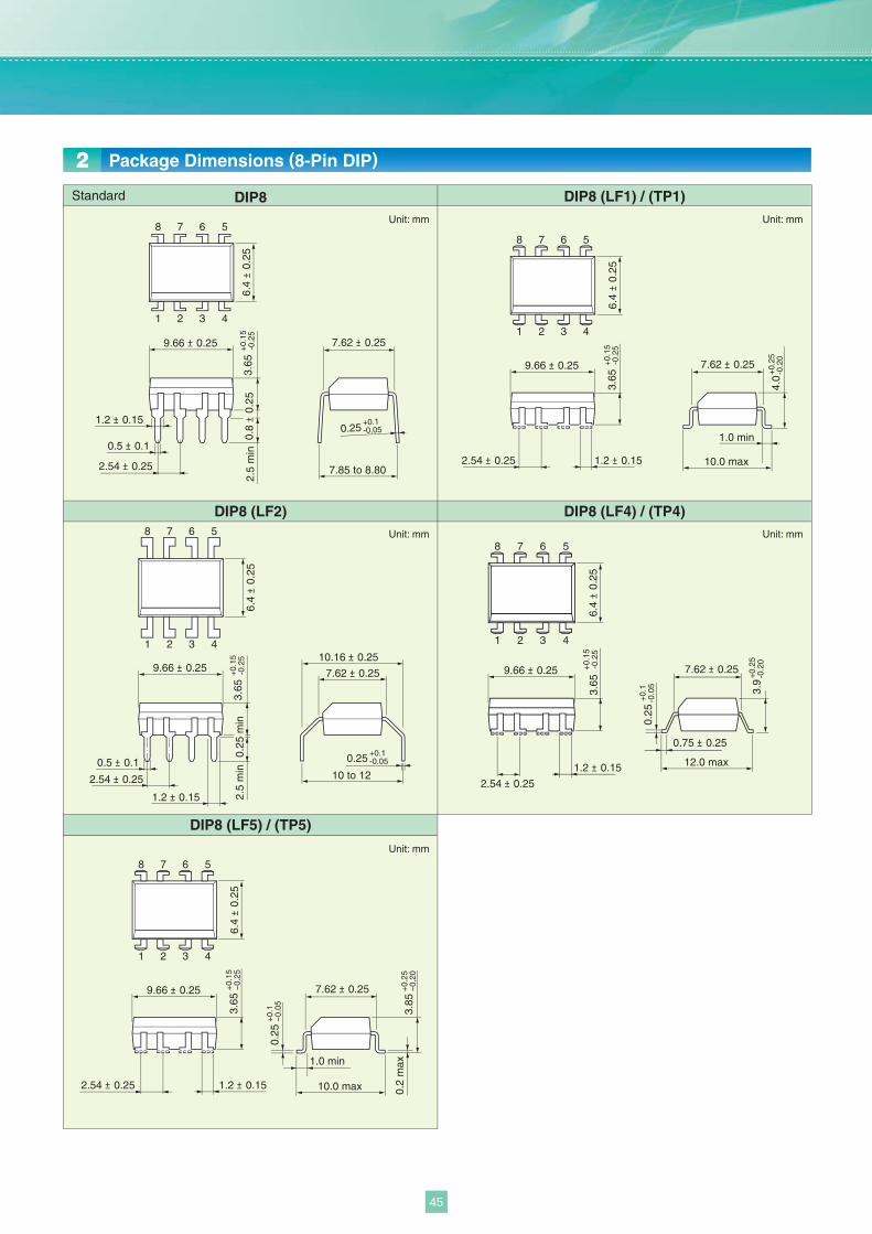
8 7 6 5
1 2
9.66 ± 0.25
3 4
6.4
± 0.
250.
8±
0.25
2.5
min
3.65
+0.
15-0
.25
2.54 ± 0.25
1.2 ± 0.15
0.5 ± 0.1
7.85 to 8.80
0.25+0.1-0.05
7.62 ± 0.25
8 7 6 5
1 2
9.66 ± 0.25
3 4
6.4
± 0.
250.
25 m
in2.
5 m
in3.
65+
0.15
-0.2
5
2.54 ± 0.25
1.2 ± 0.15
0.5 ± 0.110 to 12
0.25 +0.1-0.05
7.62 ± 0.25
10.16 ± 0.25
8 7 6 5
1 2
9.66 ± 0.25
3 4
6.4
± 0.
253.
65+
0.15
-0.2
5
2.54 ± 0.25 1.2 ± 0.15 10.0 max
1.0 min
7.62 ± 0.25
4.0
+0.
25-0
.20
8 7 6 5
1 2
9.66 ± 0.25
3 4
6.4
± 0.
25+
0.15
-0.2
5
+0.
1-0
.05
2.54 ± 0.25
1.2 ± 0.15 12.0 max
0.75 ± 0.25
7.62 ± 0.25
3.9
+0.
25-0
.20
3.65
0.25
8 7 6 5
1 2
9.66 ± 0.25
3 4
6.4
± 0.
253.
65+
0.15
-0.
25
0.25
+0.
1-
0.05
2.54 ± 0.25 1.2 ± 0.15 10.0 max 0.2
max1.0 min
7.62 ± 0.25
3.85
+0.
25-
0.20
Standard
DIP8 (LF2) DIP8 (LF4) / (TP4)
DIP8 DIP8 (LF1) / (TP1)
DIP8 (LF5) / (TP5)
Package Dimensions (8-Pin DIP)
Unit: mmUnit: mm
Unit: mmUnit: mm
Unit: mm
2
45
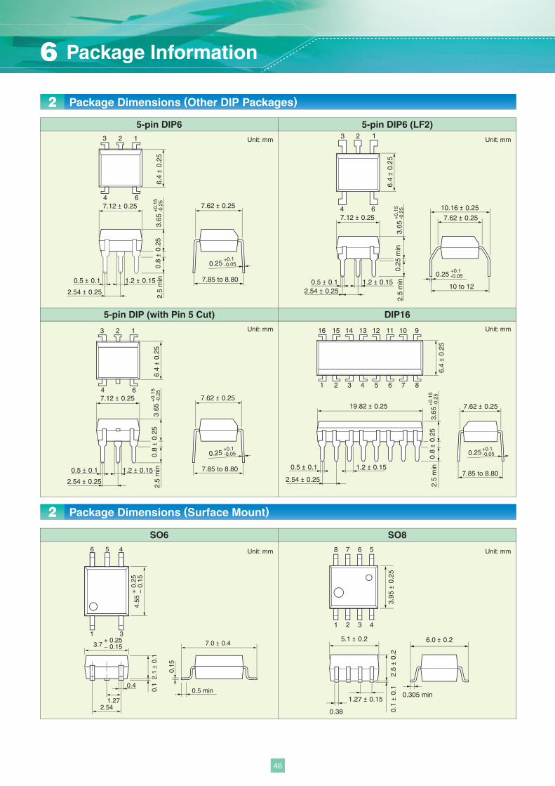
6.4
± 0.
25
7.85 to 8.80
0.25+0.1-0.05
7.62 ± 0.25
0.5 ± 0.1 1.2 ± 0.15
2.54 ± 0.25
19.82 ± 0.25
2.5
min
0.8
± 0.
253.
65+
0.15
-0.2
5
16 15 10 9
1 2 7 8
13 12 11
4 5 6
14
3
3 2 1
7.85 to 8.80
0.25+0.1-0.05
3.65
+0.
15-0
.25
7.62 ± 0.25
0.8
±0.
256.
4±
0.25
2.5
min0.5 ± 0.1 1.2 ± 0.15
2.54 ± 0.25
4 67.12 ± 0.25
4 6
10 to 12
0.25 +0.1-0.05
3.65
+0.
15-0
.25
7.62 ± 0.25
10.16 ± 0.25
0.25
min
6.4
±0.
25
2.5
min0.5 ± 0.1 1.2 ± 0.15
2.54 ± 0.25
3 2 1
7.12 ± 0.25
3 2 1
7.85 to 8.80
0.25+0.1-0.05
3.65
+0.
15-0
.25
7.62 ± 0.25
0.8
±0.
256.
4±
0.25
2.5
min0.5 ± 0.1 1.2 ± 0.15
2.54 ± 0.25
4 67.12 ± 0.25
6 4
1 3
4.55
+ 0
.25
− 0
.15
0.5 min
0.15
7.0 ± 0.43.7+ 0.25− 0.15
2.541.27
0.4
0.1
2.1
± 0.
1
5
0.305 min
6.0 ± 0.25.1 ± 0.2
0.38
1.27 ± 0.15
0.1
± 0.
12.
5±
0.2
3.95
± 0.
25
8 567
1 432
DIP165-pin DIP (with Pin 5 Cut)
SO6 SO8
5-pin DIP6 5-pin DIP6 (LF2)
Package Dimensions (Other DIP Packages)
Package Dimensions (Surface Mount)
Unit: mmUnit: mm
Unit: mmUnit: mm
Unit: mm Unit: mm
2
2
6 Package Information
46
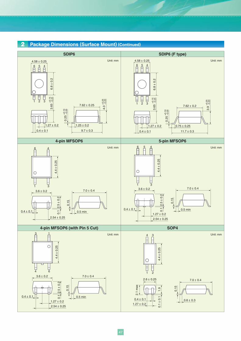
7.0 ± 0.4
0.6 ± 0.3
0.15
4 3
1 2
4.4
± 0.
25
2.6 ± 0.25
2.1
max
0.4 ± 0.1
1.27 ± 0.2
0.1
± 0.
11.
9
4.58 ± 0.25
0.4 ± 0.1
1.27 ± 0.2 1.25 ± 0.2
7.62 ± 0.25
6.8
± 0.
23.
65
9.7 ± 0.3
1 2 3
6 5 4
+0.
15-
0.25
0.25
+0.
10-
0.05
4.0
+0.
25-
0.20
4.58 ± 0.25
6.8
± 0.
2
1 2 3
6 5 4
0.4 ± 0.1
1.27 ± 0.2
3.65
+0.
15-
0.25
0.75 ± 0.25
7.62 ± 0.2
11.7 ± 0.3
0.25
+0.
10-
0.05
3.9
+0.
25-
0.20
6 5 4
1 3
4.4
± 0.
25
0.5 min
0.15
7.0 ± 0.43.6 ± 0.2
0.1
2.5
± 0.
2
0.4 ± 0.1
1.27 ± 0.2
2.54 ± 0.25
6 4
1 3
4.4
± 0.
25
0.5 min
0.15
7.0 ± 0.43.6 ± 0.2
0.4 ± 0.1
0.1
2.5
± 0.
2
2.54 ± 0.25
7.0 ± 0.4
3 1
4 6
4.4
± 0.
25
0.5 min
0.15
3.6 ± 0.2
1.27 ± 0.2
0.1
2.5
± 0.
2
0.4 ± 0.1
2.54 ± 0.25
4-pin MFSOP6
SDIP6 (F type)
4-pin MFSOP6 (with Pin 5 Cut)
5-pin MFSOP6
SOP4
SDIP6
Package Dimensions (Surface Mount) (Continued)
Unit: mmUnit: mm
Unit: mmUnit: mm
Unit: mmUnit: mm
2
47
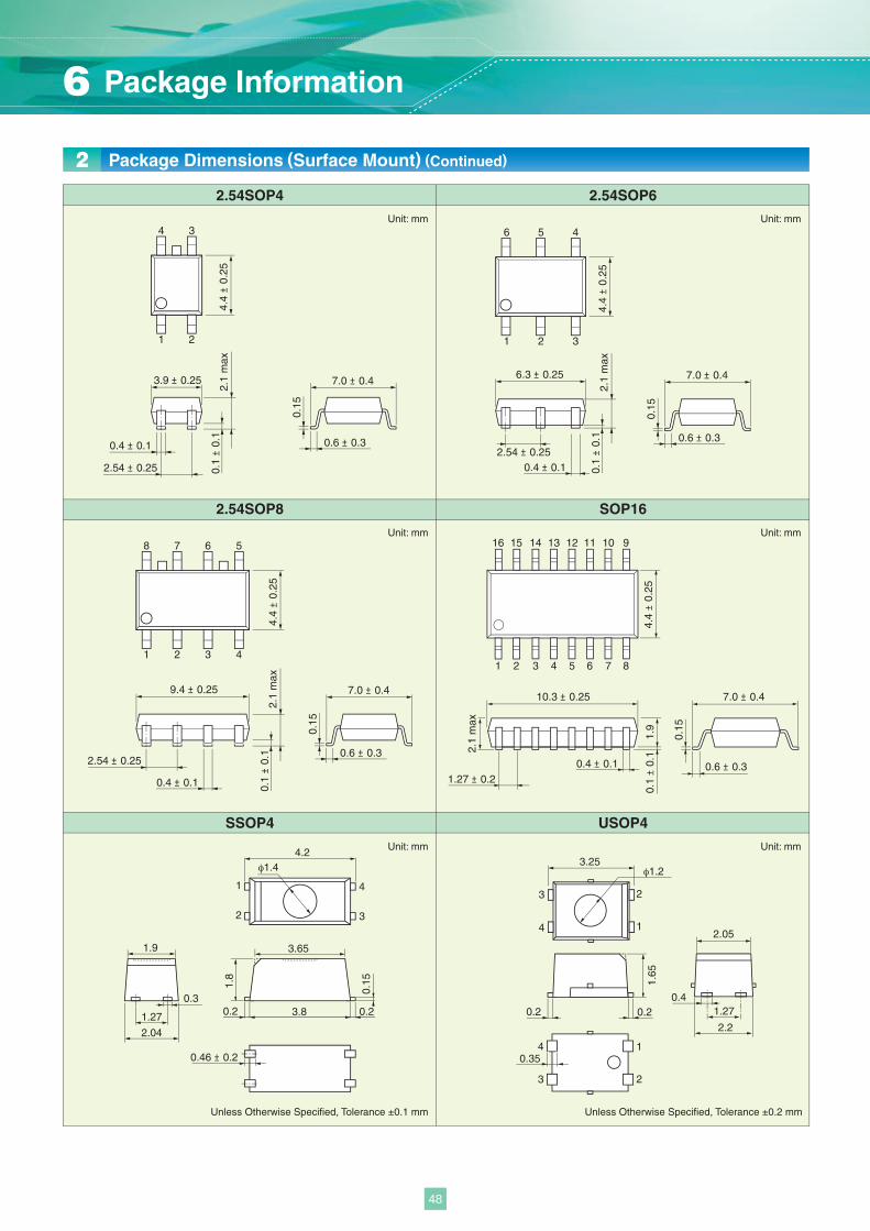
0.15
0.6 ± 0.3
7.0 ± 0.49.4 ± 0.25
2.1
max
0.1
± 0.
1
2.54 ± 0.25
0.4 ± 0.1
8 7 6 5
4.4
± 0.
25
1 2 3 40.
15
0.6 ± 0.3
7.0 ± 0.4
4.4
± 0.
25
6 5 4
1 2 3
6.3 ± 0.25
2.1
max
0.1
± 0.
1
2.54 ± 0.250.4 ± 0.1
φ1.44.2
0.46 ± 0.2
1
2
3.651.9
2.04
1.27
0.33.80.2 0.2
1.8
0.15
4
3
1516 10 9
21 7 8
12 11
5 6
1314
43
7.0 ± 0.4
0.6 ± 0.3
0.15
4.4
± 0.
25
10.3 ± 0.25
2.1
max
0.4 ± 0.11.27 ± 0.2
0.1
± 0.
11.
9
0.15
0.6 ± 0.3
7.0 ± 0.43.9 ± 0.25
2.1
max
0.1
± 0.
1
2.54 ± 0.25
0.4 ± 0.1
4 3
1 2
4.4
± 0.
25
φ1.23.25
0.35
3
4
2.05
2.2
1.270.4
0.2 0.2
1.65
2
1
3
4
2
1
2.54SOP62.54SOP4
2.54SOP8 SOP16
SSOP4
Package Dimensions (Surface Mount) (Continued)
Unit: mmUnit: mm
Unit: mmUnit: mm
Unit: mm Unit: mm
Unless Otherwise Specified, Tolerance ±0.2 mmUnless Otherwise Specified, Tolerance ±0.1 mm
2
USOP4
6 Package Information
48
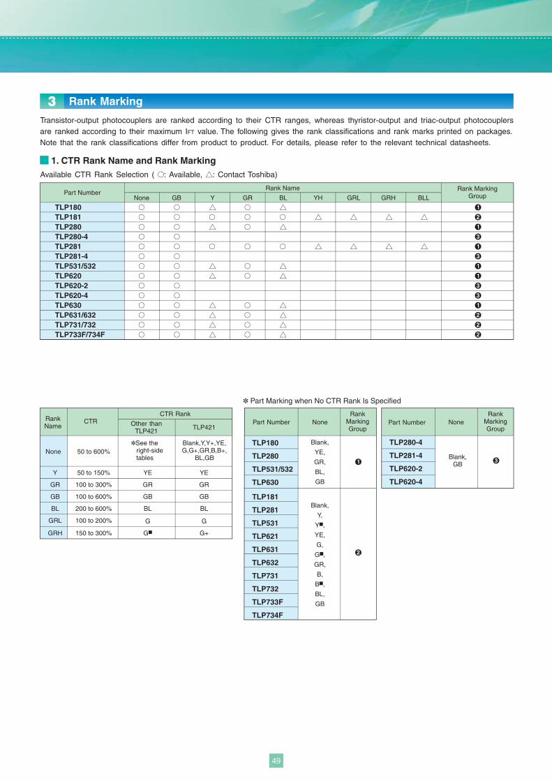
Rank Marking
Transistor-output photocouplers are ranked according to their CTR ranges, whereas thyristor-output and triac-output photocouplers are ranked according to their maximum IFT value. The following gives the rank classifications and rank marks printed on packages.Note that the rank classifications differ from product to product. For details, please refer to the relevant technical datasheets.
Available CTR Rank Selection ( ●: Available, ▲: Contact Toshiba)
✽ Part Marking when No CTR Rank Is Specified
TLP180TLP181TLP280TLP280-4TLP281TLP281-4TLP531/532TLP620TLP620-2TLP620-4TLP630TLP631/632TLP731/732TLP733F/734F
Part NumberRank Marking
GroupNone GB Y GR BL YH GRL GRH BLL
Rank Name
None
Y
GR
GB
BL
GRL
GRH
RankName
50 to 600%
50 to 150%
100 to 300%
100 to 600%
200 to 600%
100 to 200%
150 to 300%
CTR Other thanTLP421
✽See the right-side tables
YE
GR
GB
BL
G
G■
YE
GR
GB
BL
G
G+
Blank,Y,Y+,YE,G,G+,GR,B,B+,
BL,GB
TLP421
Blank,
Y,
Y■,
YE,
G,
G■,
GR,
B,
B■,
BL,
GB
Blank,
YE,
GR,
BL,
GB
NoneRank
MarkingGroup
Part Number NoneRank
MarkingGroup
Part Number
TLP180
TLP280
TLP531/532
TLP630
TLP181
TLP281
TLP531
TLP621
TLP631
TLP632
TLP731
TLP732
TLP733F
TLP734F
Blank,GB
TLP280-4
TLP281-4
TLP620-2
TLP620-4
CTR Rank
1
1
1
1
1
1
3
3
3
3
3
2
2
1
2
2
2
1. CTR Rank Name and Rank Marking
3
49
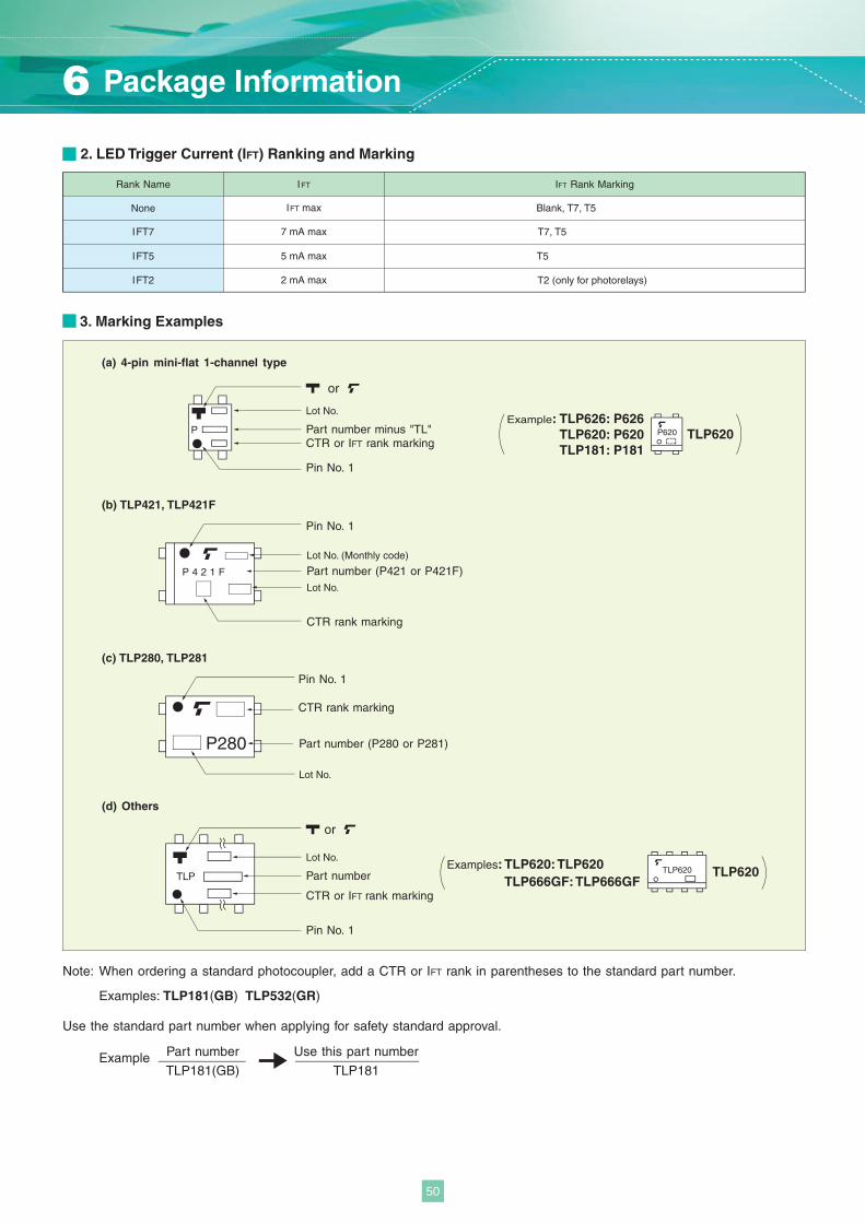
P
Lot No.
Part number minus "TL"CTR or IFT rank marking
Pin No. 1
or
P 4 2 1 F
Lot No. (Monthly code)
Part number (P421 or P421F)Lot No.
CTR rank marking
Pin No. 1
Lot No.
CTR rank marking
Part number (P280 or P281)
Pin No. 1
TLP620TLP
Lot No.
Part number
CTR or IFT rank marking
or
Pin No. 1
(a) 4-pin mini-flat 1-channel type
(d) Others
(b) TLP421, TLP421F
(c) TLP280, TLP281
P620Example: TLP626: P626 TLP620: P620 TLP181: P181
TLP620
Examples: TLP620: TLP620 TLP666GF: TLP666GF
TLP620
P280
3. Marking Examples
Note: When ordering a standard photocoupler, add a CTR or IFT rank in parentheses to the standard part number.
Examples: TLP181(GB) TLP532(GR)
Use the standard part number when applying for safety standard approval.
Example Part number
TLP181(GB)
Use this part number
TLP181
2. LED Trigger Current (IFT) Ranking and Marking
7 mA max
IFT max
5 mA max
2 mA max
Blank, T7, T5
T7, T5
T5
T2 (only for photorelays)
Rank Name
None
IFT7
IFT5
IFT2
IFT IFT Rank Marking
6 Package Information
50
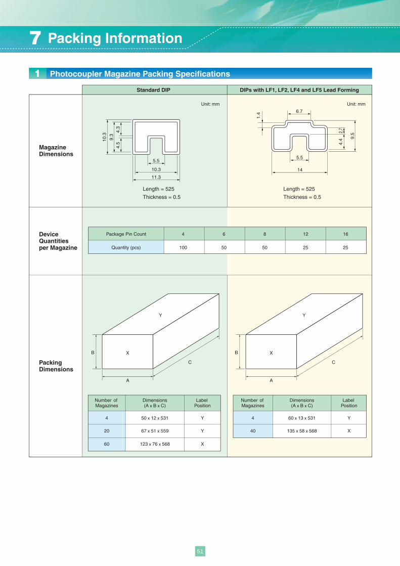
1
11.3
10.3
5.5
10.3
9.3
4.5
4.3
14
5.5
6.7
2.7
4.4 9.
5
1.4
B
A
X
Y
C
B
A
X
Y
C
Photocoupler Magazine Packing Specifications
Standard DIP DIPs with LF1, LF2, LF4 and LF5 Lead Forming
MagazineDimensions
DeviceQuantitiesper Magazine
Packing Dimensions
Length = 525
Thickness = 0.5
Length = 525
Thickness = 0.5
Unit: mm Unit: mm
60 x 13 x 531
135 x 58 x 568
Dimensions(A x B x C)
LabelPosition
Y
X
4
40
Number of Magazines
50 x 12 x 531
67 x 51 x 559
123 x 76 x 568
Dimensions(A x B x C)
Y
Y
X
LabelPosition
4
20
60
Number of Magazines
Package Pin Count
Quantity (pcs)
4
100
6
50
8
50
12
25
16
25
7 Packing Information
51
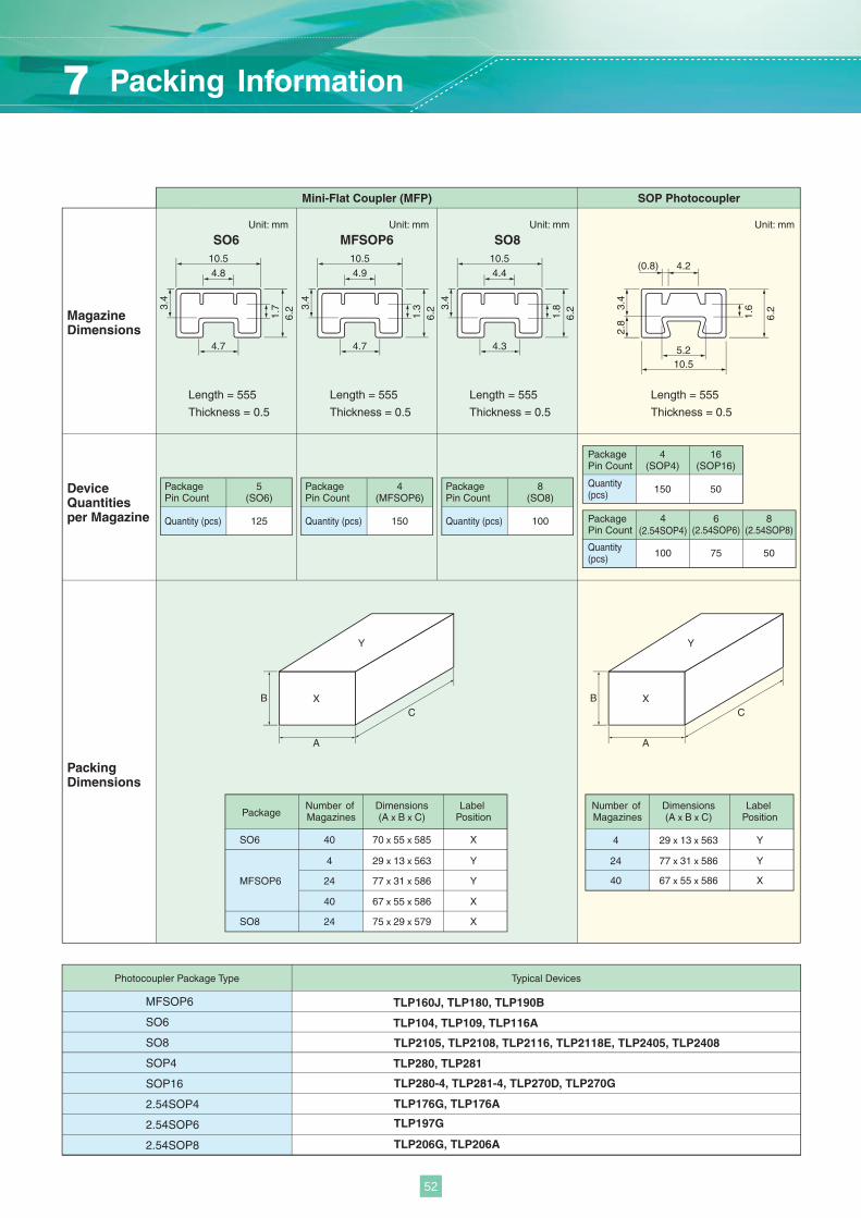
B
A
X
Y
CB
A
X
Y
C
10.54.9
4.7
3.4
6.2
1.3
10.5
4.2(0.8)
5.2
2.8
3.4
6.2
1.6
10.54.8
4.7
3.4
6.2
1.7
10.54.4
4.3
3.4
6.2
1.8
Mini-Flat Coupler (MFP) SOP Photocoupler
MagazineDimensions
DeviceQuantitiesper Magazine
Packing Dimensions
Length = 555
Thickness = 0.5
Length = 555
Thickness = 0.5
Length = 555
Thickness = 0.5
Unit: mmUnit: mmUnit: mm Unit: mm
4
24
40
Y
Y
X
29 x 13 x 563
77 x 31 x 586
67 x 55 x 586
Dimensions(A x B x C)
LabelPosition
Number of Magazines
40
4
24
X
Y
Y
70 x 55 x 585
29 x 13 x 563
77 x 31 x 586
40 X67 x 55 x 586
24
SO6
MFSOP6
SO8 X75 x 29 x 579
Dimensions(A x B x C)
LabelPosition
Number of MagazinesPackage
Package Pin Count
Quantity (pcs)
5(SO6)
125
Package Pin Count
Quantity (pcs)
4(MFSOP6)
150
Package Pin Count
Quantity (pcs)
8(SO8)
100
Quantity(pcs)
TLP160J, TLP180, TLP190B
TLP104, TLP109, TLP116A
TLP176G, TLP176A
TLP206G, TLP206A
TLP197G
TLP2105, TLP2108, TLP2116, TLP2118E, TLP2405, TLP2408
TLP280, TLP281
TLP280-4, TLP281-4, TLP270D, TLP270G
Typical DevicesPhotocoupler Package Type
PackagePin Count
Quantity(pcs)
PackagePin Count
4(SOP4)
16(SOP16)
6(2.54SOP6)
4(2.54SOP4)
8(2.54SOP8)
150 50
100 75 50
MFSOP6
SO6
SO8
SOP4
SOP16
2.54SOP4
2.54SOP6
2.54SOP8
SO6 MFSOP6 SO8
Length = 555
Thickness = 0.5
7 Packing Information
52
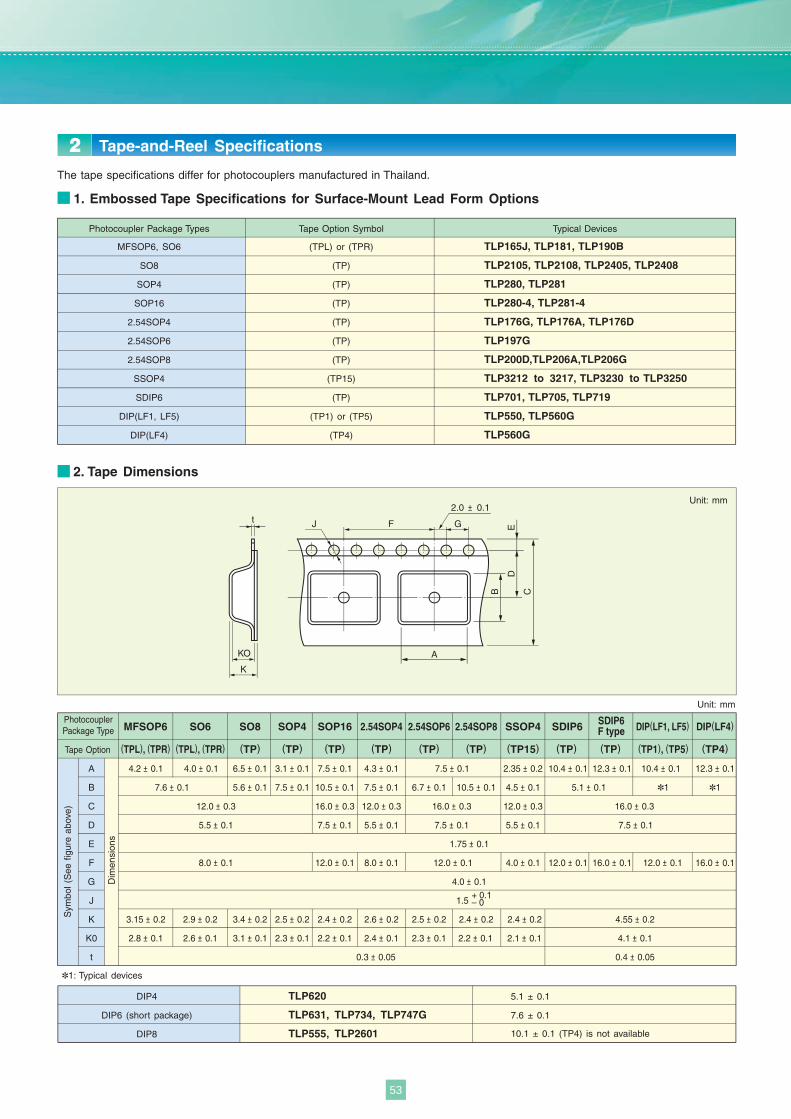
t
KO
K
J F
A
G
DE
CB
2.0 ± 0.1
2 Tape-and-Reel Specifications
The tape specifications differ for photocouplers manufactured in Thailand.
1. Embossed Tape Specifications for Surface-Mount Lead Form Options
2. Tape Dimensions
Unit: mm
Unit: mm
✽1: Typical devices
Photocoupler Package Types
MFSOP6, SO6
SO8
SOP16
2.54SOP4
2.54SOP6
2.54SOP8
DIP(LF1, LF5)
DIP(LF4)
Tape Option Symbol
(TPL) or (TPR)
(TP)
(TP)
(TP)
(TP)
(TP)
(TP1) or (TP5)
(TP4)
Typical Devices
TLP165J, TLP181, TLP190B
TLP2105, TLP2108, TLP2405, TLP2408
SOP4 (TP) TLP280, TLP281
TLP280-4, TLP281-4
TLP176G, TLP176A, TLP176D
TLP197G
TLP200D,TLP206A,TLP206G
TLP550, TLP560G
SSOP4 (TP15) TLP3212 to 3217, TLP3230 to TLP3250
SDIP6 (TP) TLP701, TLP705, TLP719
TLP560G
A
B
PhotocouplerPackage Type
Tape Option
MFSOP6
(TPL), (TPR)
4.2 ± 0.1
SO6
(TPL), (TPR)
4.0 ± 0.1
7.6 ± 0.1
C
D
SOP4
(TP)
SO8
(TP)
SOP16
(TP)
2.54SOP4
(TP)
2.54SOP6
(TP)
2.54SOP8 SSOP4
(TP) (TP15)
SDIP6
(TP)
SDIP6F type
(TP)
2.5 ± 0.2
2.3 ± 0.1
2.4 ± 0.2 2.4 ± 0.2
2.2 ± 0.1 2.1 ± 0.1
4.55 ± 0.2
4.1 ± 0.1
0.4 ± 0.050.3 ± 0.05
DIP(LF1, LF5)
(TP1), (TP5)
DIP(LF4)
(TP4)
3.1 ± 0.1
7.5 ± 0.1
6.5 ± 0.1
5.6 ± 0.1
7.5 ± 0.1
10.5 ± 0.1
4.3 ± 0.1
7.5 ± 0.1
3.15 ± 0.2
2.8 ± 0.1
2.5 ± 0.2
2.3 ± 0.1
3.4 ± 0.2
3.1 ± 0.1
2.9 ± 0.2
2.6 ± 0.1
2.4 ± 0.2
2.2 ± 0.1
2.6 ± 0.2
2.4 ± 0.1
16.0 ± 0.3
7.5 ± 0.1
12.0 ± 0.3
5.5 ± 0.1
8.0 ± 0.1
12.0 ± 0.3
5.5 ± 0.1
1.75 ± 0.1
4.0 ± 0.1
1.5
12.0 ± 0.3
5.5 ± 0.1
16.0 ± 0.3
7.5 ± 0.1
16.0 ± 0.3
7.5 ± 0.1
12.0 ± 0.1 8.0 ± 0.1
6.7 ± 0.1
7.5 ± 0.1
10.5 ± 0.1
4.0 ± 0.112.0 ± 0.1 12.0 ± 0.1
10.4 ± 0.12.35 ± 0.2
4.5 ± 0.1 5.1 ± 0.1
12.0 ± 0.1
10.4 ± 0.1
16.0 ± 0.1
12.3 ± 0.1 12.3 ± 0.1
E
F
G
J
K
K0
t
DIP4
DIP6 (short package)
DIP8
TLP620
TLP631, TLP734, TLP747G
TLP555, TLP2601
5.1 ± 0.1
7.6 ± 0.1
10.1 ± 0.1 (TP4) is not available
+ 0.1– 0
16.0 ± 0.1
Sym
bol (
See
fig
ure
abov
e)
Dim
ensi
ons
✽1 ✽1
53
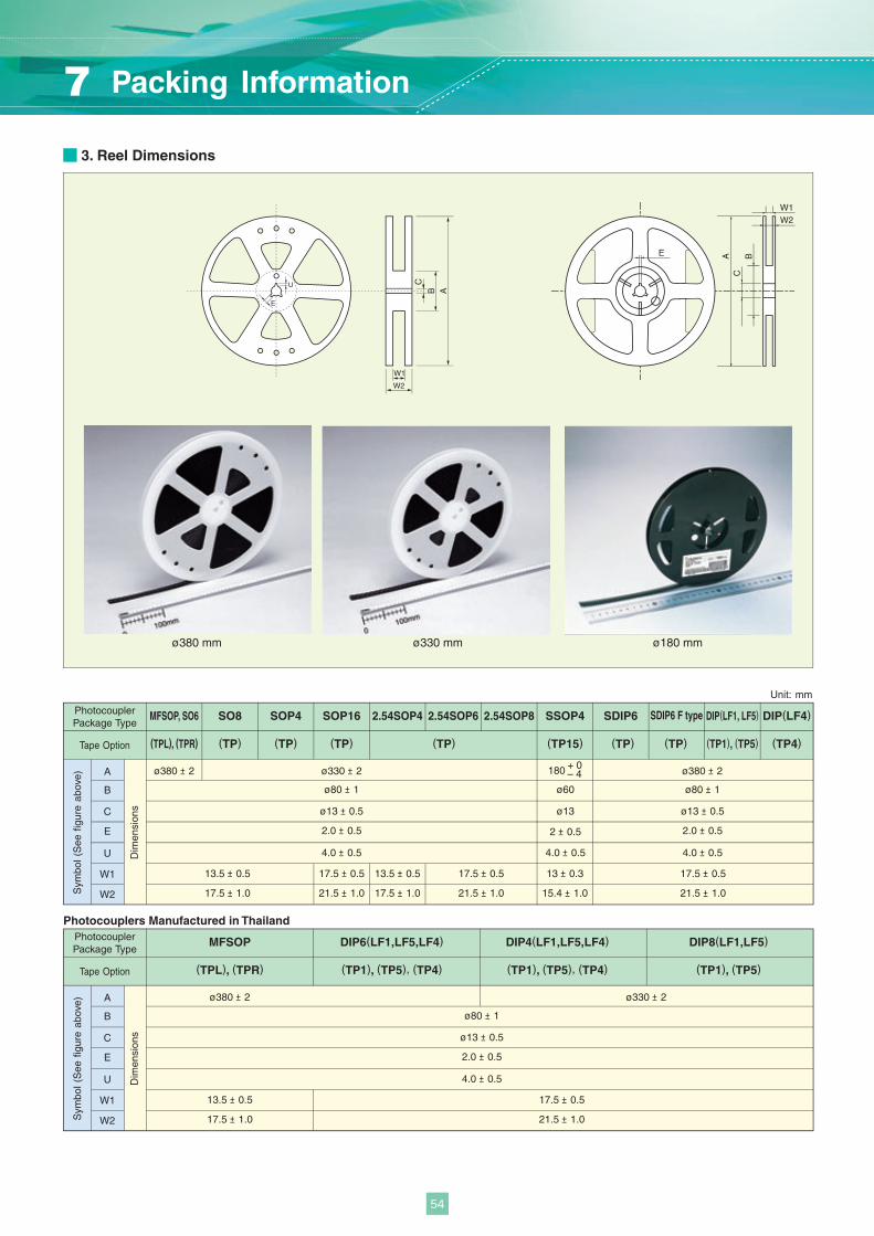
E
U
W2
W1
C
B A
BC
E A
W2W1
ø380 mm ø330 mm ø180 mm
ø380 ± 2
ø80 ± 1
ø13 ± 0.5
2.0 ± 0.5
4.0 ± 0.5
ø60
ø13
4.0 ± 0.5
2 ± 0.5
ø80 ± 1
ø13 ± 0.5
2.0 ± 0.5
4.0 ± 0.5
13.5 ± 0.5
17.5 ± 1.0
ø380 ± 2
13.5 ± 0.5
17.5 ± 1.0
13 ± 0.3
15.4 ± 1.0
17.5 ± 0.5
21.5 ± 1.0
17.5 ± 0.5
21.5 ± 1.0
ø330 ± 2
B
C
E
U
W1
W2
A
17.5 ± 0.5
21.5 ± 1.0
Unit: mm
PhotocouplerPackage Type
Tape Option
MFSOP, SO6
(TPL), (TPR)
SOP4
(TP)
SO8
(TP)
SOP16
(TP)
2.54SOP4
(TP) (TP) (TP)(TP15)
DIP(LF4)
(TP4)
DIP(LF1, LF5)2.54SOP8 SSOP4 SDIP6 SDIP6 F type2.54SOP6
(TP1), (TP5)
180 + 0– 4
Sym
bol (
See
fig
ure
abov
e)
Dim
ensi
ons
ø380 ± 2
ø80 ± 1
ø13 ± 0.5
2.0 ± 0.5
4.0 ± 0.5
13.5 ± 0.5
17.5 ± 1.0
ø330 ± 2
B
C
E
U
W1
W2
A
17.5 ± 0.5
21.5 ± 1.0
PhotocouplerPackage Type
Tape Option
MFSOP
(TPL), (TPR)
DIP6(LF1,LF5,LF4)
(TP1), (TP5), (TP4)
DIP4(LF1,LF5,LF4)
(TP1), (TP5), (TP4) (TP1), (TP5)
DIP8(LF1,LF5)
Sym
bol (
See
fig
ure
abov
e)
Dim
ensi
ons
Photocouplers Manufactured in Thailand
3. Reel Dimensions
7 Packing Information
54
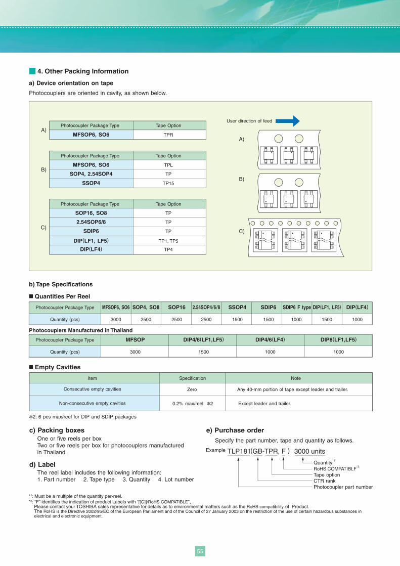
User direction of feed
A)
B)
C)
4. Other Packing Information
a) Device orientation on tape
Photocouplers are oriented in cavity, as shown below.
b) Tape Specifications
SOP16, SO8
2.54SOP6/8
SDIP6
MFSOP6, SO6
SOP4, 2.54SOP4
Photocoupler Package Type
MFSOP6, SO6
DIP(LF1, LF5)
DIP(LF4)
TP
TP
TP
TPL
TP
SSOP4 TP15
Tape Option
Photocoupler Package Type Tape Option
Photocoupler Package Type Tape Option
TPR
TP1, TP5
TP4
A)
B)
C)
■ Quantities Per Reel
■ Empty Cavities
✽2: 6 pcs max/reel for DIP and SDIP packages
Item
Consecutive empty cavities
Non-consecutive empty cavities
Specification
Zero
0.2% max/reel ✽2
Note
Any 40-mm portion of tape except leader and trailer.
Except leader and trailer.
Photocoupler Package Type
Quantity (pcs)
MFSOP6, SO6
3000
SOP4, SO8
2500
SOP16
2500
SSOP4
1500
2.54SOP4/6/8
2500
DIP(LF1, LF5)
1500
DIP(LF4)
1000
SDIP6
1500
SDIP6 F type
1000
Photocouplers Manufactured in Thailand
Photocoupler Package Type
Quantity (pcs)
MFSOP
3000
DIP4/6(LF1,LF5)
1500
DIP4/6(LF4)
1000
DIP8(LF1,LF5)
1000
c) Packing boxes
d) Label
One or five reels per boxTwo or five reels per box for photocouplers manufactured in Thailand
The reel label includes the following information:1. Part number 2. Tape type 3. Quantity 4. Lot number
*1: Must be a multiple of the quantity per-reel.*2: “F” identifies the indication of product Labels with “[[G]]/RoHS COMPATIBLE”.
Please contact your TOSHIBA sales representative for details as to environmental matters such as the RoHS compatibility of Product.The RoHS is the Directive 2002/95/EC of the European Parliament and of the Council of 27 January 2003 on the restriction of the use of certain hazardous substances in electrical and electronic equipment.
e) Purchase orderSpecify the part number, tape and quantity as follows.
Example TLP181 3000 units(GB-TPR, F )
Quantity*1
RoHS COMPATIBLF*2
Tape optionCTR rankPhotocoupler part number
55
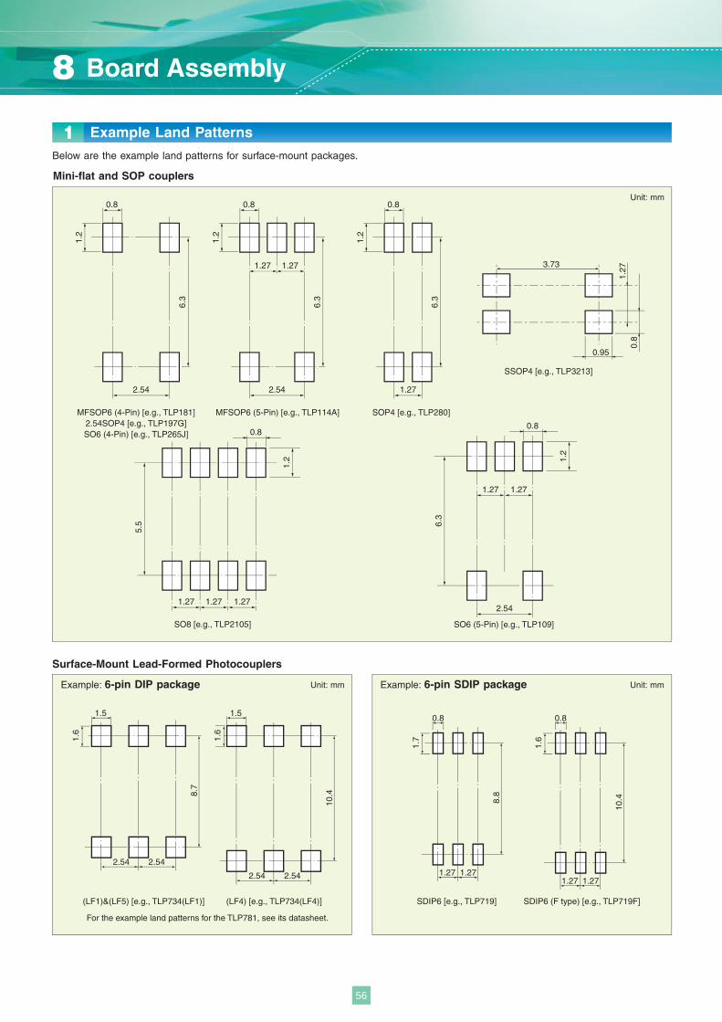
2.54 2.54
1.5
1.6
10.4
2.54 2.54
1.5
1.6
8.7
1.27 1.27
0.8
1.7
8.8
1.27 1.27
0.8
1.6
10.4
MFSOP6 (4-Pin) [e.g., TLP181]2.54SOP4 [e.g., TLP197G]SO6 (4-Pin) [e.g., TLP265J]
MFSOP6 (5-Pin) [e.g., TLP114A]
SO6 (5-Pin) [e.g., TLP109]
SOP4 [e.g., TLP280]
SO8 [e.g., TLP2105]
(LF1)&(LF5) [e.g., TLP734(LF1)] (LF4) [e.g., TLP734(LF4)] SDIP6 [e.g., TLP719] SDIP6 (F type) [e.g., TLP719F]
For the example land patterns for the TLP781, see its datasheet.
0.8
2.54
1.2
6.3
0.8
1.27 1.27
2.54
1.2
6.3
0.8
1.27
1.2
6.3
0.8
2.54
1.271.27
1.2
6.3
0.8
1.271.271.27
1.2
5.5
1.27
0.8
3.73
0.95
SSOP4 [e.g., TLP3213]
1 Example Land Patterns
Mini-flat and SOP couplers
Surface-Mount Lead-Formed Photocouplers
Below are the example land patterns for surface-mount packages.
Unit: mm
Unit: mmUnit: mmExample: 6-pin DIP package Example: 6-pin SDIP package
8 Board Assembly
56
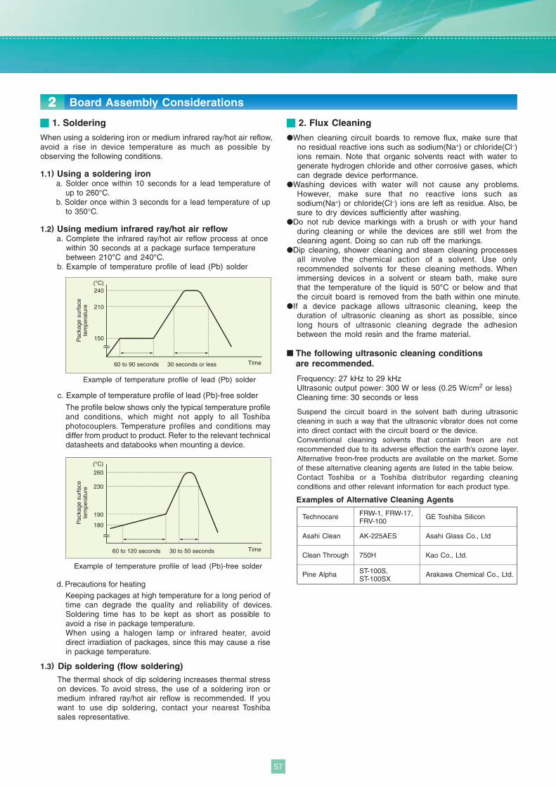
Example of temperature profile of lead (Pb) solder
(°C)240
210
150Pac
kage
sur
face
tem
pera
ture
60 to 90 seconds 30 seconds or less Time
Example of temperature profile of lead (Pb)-free solder
(°C)
260
230
180
190
Pac
kage
sur
face
tem
pera
ture
60 to 120 seconds 30 to 50 seconds Time
Board Assembly Considerations
1. Soldering 2. Flux Cleaning
When using a soldering iron or medium infrared ray/hot air reflow, avoid a rise in device temperature as much as possible by observing the following conditions.
1.1) Using a soldering irona. Solder once within 10 seconds for a lead temperature of
up to 260°C.b. Solder once within 3 seconds for a lead temperature of up
to 350°C.
1.2) Using medium infrared ray/hot air reflowa. Complete the infrared ray/hot air reflow process at once
within 30 seconds at a package surface temperature between 210°C and 240°C.
b. Example of temperature profile of lead (Pb) solder
●When cleaning circuit boards to remove flux, make sure that no residual reactive ions such as sodium(Na+) or chloride(Cl–)ions remain. Note that organic solvents react with water to generate hydrogen chloride and other corrosive gases, which can degrade device performance.
●Washing devices with water will not cause any problems. However, make sure that no reactive ions such as sodium(Na+) or chloride(Cl–) ions are left as residue. Also, be sure to dry devices sufficiently after washing.
●Do not rub device markings with a brush or with your hand during cleaning or while the devices are still wet from the cleaning agent. Doing so can rub off the markings.
●Dip cleaning, shower cleaning and steam cleaning processes all involve the chemical action of a solvent. Use only recommended solvents for these cleaning methods. When immersing devices in a solvent or steam bath, make sure that the temperature of the liquid is 50°C or below and that the circuit board is removed from the bath within one minute.
●If a device package allows ultrasonic cleaning, keep the duration of ultrasonic cleaning as short as possible, since long hours of ultrasonic cleaning degrade the adhesion between the mold resin and the frame material.
Suspend the circuit board in the solvent bath during ultrasonic cleaning in such a way that the ultrasonic vibrator does not come into direct contact with the circuit board or the device.Conventional cleaning solvents that contain freon are not recommended due to its adverse effection the earth’s ozone layer. Alternative freon-free products are available on the market. Some of these alternative cleaning agents are listed in the table below.Contact Toshiba or a Toshiba distributor regarding cleaning conditions and other relevant information for each product type.
1.3) Dip soldering (flow soldering)
Keeping packages at high temperature for a long period of time can degrade the quality and reliability of devices. Soldering time has to be kept as short as possible to avoid a rise in package temperature.When using a halogen lamp or infrared heater, avoid direct irradiation of packages, since this may cause a rise in package temperature.
The thermal shock of dip soldering increases thermal stress on devices. To avoid stress, the use of a soldering iron or medium infrared ray/hot air reflow is recommended. If you want to use dip soldering, contact your nearest Toshiba sales representative.
d. Precautions for heating
The profile below shows only the typical temperature profile and conditions, which might not apply to all Toshiba photocouplers. Temperature profiles and conditions may differ from product to product. Refer to the relevant technical datasheets and databooks when mounting a device.
■ The following ultrasonic cleaning conditions are recommended.
Frequency: 27 kHz to 29 kHzUltrasonic output power: 300 W or less (0.25 W/cm2 or less)Cleaning time: 30 seconds or less
Examples of Alternative Cleaning Agents
Technocare GE Toshiba Silicon
Asahi Clean Asahi Glass Co., Ltd
Clean Through
AK-225AES
750H Kao Co., Ltd.
Pine Alpha Arakawa Chemical Co., Ltd.
FRW-1, FRW-17, FRV-100
ST-100S, ST-100SX
c. Example of temperature profile of lead (Pb)-free solder
2
57
1Toshiba photocouplers use one of four types of LEDs and a projection of the operating life has been made for each LED. The table on page 57 shows the types of LED used in photocouplers and the figures on pages 58 to 60 show projections of long-term light output performance and operating life. Note that these operating life data are estimates extrapolated from long-term light output degradation over a single wafer lot and are shown as reference only.
F50% operating life
1,300,000 h
540,000 h
1,000,000 h
260,000 h
100,000 h
200,000 h
Projected Operating Life Ta = 40°C, IF = 20 mA, failure criteria:
degradation rate Δ PO < –50%
F0.1% operating life
Photocouplers
GaAs LED
GaA As(SH) LED
GaA As(DH) LED3
1
2
Projected Operating Life Based on LED Light Output Degradation
Mainly for phototransistor output devices
and phototriac output devices
Mainly for photorelays (MOSFET output),
photovoltaic couplers and photo-IC couplers
Mainly for photo-IC couplers
Ask your local Toshiba sales representative.GaA As(MQW) LED4 Mainly for photo-IC couplers
F50% (cumulative failure rate 50%) operating life: Time period until the projected long-term light output degradation curve of the average light output change (X) shown on pages 58 to 60 reaches the failure criteria.
F0.1% (cumulative failure rate 0.1%) operating life: Time period until the projected long-term light output degradation curve of X - 3σ shown on pages 58 to 60 reaches the failure criteria.
The relationship between LED light output degradation and optical coupling characteristics is shown below.
(1) The relationship between LED light output degradation
and current transfer ratio (CTR)/short circuit current (ISC) is 1:1.
CTR (t)
CTR (o)
Po (t)
Po (o)=
(2) The relationship between a reciprocal value of LED light output degradation
and IFT/IFLH/IFHL/IFH change is 1:1. IFT ( t )
IFT (o)
Po (t)
Po (o)= ( )-1
9 Device Degradation
58
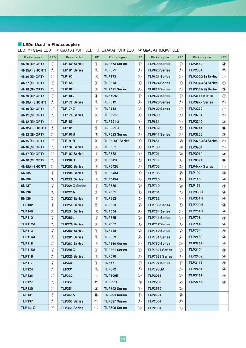
LEDs Used in PhotocouplersLED: GaAs LED GaA As (SH) LED 31 2 GaA As (DH) LED 4 GaA As (MQW) LED
4N25 (SHORT)
4N25A (SHORT)
4N26 (SHORT)
4N27 (SHORT)
4N28 (SHORT)
4N29 (SHORT)
4N29A (SHORT)
4N30 (SHORT)
4N31 (SHORT)
4N32 (SHORT)
4N32A (SHORT)
4N33 (SHORT)
4N35 (SHORT)
4N36 (SHORT)
4N37 (SHORT)
4N38 (SHORT)
4N38A (SHORT)
6N135
6N136
6N137
6N138
6N139
TLP102
TLP106
TLP112
TLP112A
TLP113
TLP114A
TLP115
TLP116TLP116
TLP117
TLP115A
TLP124
TLP126
TLP127
TLP130
TLP131
TLP137
LED
TLP141G
TLP160 Series
TLP161 Series
TLP163
TLP165J
TLP166J
TLP168J
TLP172 Series
TLP174G
TLP176 Series
TLP180
TLP181
TLP190B
TLP191B
TLP192 Series
TLP197 Series
TLP200D
TLP202 Series
TLP206 Series
TLP222 Series
TLP224G Series
TLP225A
TLP227 Series
TLP250 Series
TLP251 Series
TLP260J
TLP270 Series
TLP280 Series
TLP281 Series
TLP283 Series
TLP296G
TLP320 Series
LED
TLP330
TLP331
TLP371
TLP372
TLP373
TLP421 Series
TLP504A
TLP512
TLP513
TLP521-1
TLP521-2
TLP521-4
TLP523 Series
TLP525G Series
TLP531
TLP532
TLP541G
TLP542G
TLP543J
TLP545J
TLP550
TLP551
TLP552
TLP553
TLP554
TLP555
TLP557
TLP558
TLP559
LED
TLP560 Series
TLP561 Series
TLP570
TLP594 Series
TLP597 Series
TLP598 Series
TLP599 Series
TLP620 Series
TLP621 Series
TLP624 Series
TLP626 Series
TLP627 Series
TLP628 Series
TLP629 Series
TLP630
TLP631
TLP632
TLP641 Series
TLP3022(S) Series
TLP651
TLP731
TLP719
TLP705
TLP701
TLP700
TLP732
TLP733 Series
LED
TLP734 Series
TLP741 Series
TLP763J Series
TLP797 Series
TLP798GA
TLP2200
TLP2066
TLP2530
TLP2531
TLP2601
TLP260J
TLP2630
TLP2631
TLP31xx Series
TLP32xx Series
TLP4xxx Series
LED
TLP3762(S) Series
TLP3063(S) Series
TLP3042(S) Series
3
3
3
3
3
1
1
1
1
1
1
1
1
1
1
1
1
1
1
1
1
1
1
1
1
1
1
1
2
2
2
2
2
2
2
2
2
2
TLP3230
TLP3231
TLP3240
TLP3241
TLP3250
TLP706
TLP716
TLP702
1
1
1
1
1
1
1
1
1
1
1
1
1
1
1
1
1
1
1
2
2
2
2
2
2
2
2
2
2
2
1
1
1
3
3
3
1
1
1
1
1
1
1
1
1
1
1
1
1
1
1
1
1
1
1
1
1
1
1
1
1
1
1
1
1
2
2
TLP332
TLP351
TLP351A
TLP360 Series
TLP361 Series
TLP363 Series
TLP350
1
2
2
2
TLP571
TLP572
TLP590B
TLP591B
3
3
1
1
TLP592 Series
TLP747 Series
TLP750 Series
TLP759 Series
TLP762J Series
3
1
1
1
1
1
1
1
1
1
1
1
1
1
1
1
2
3
1
1
1
1
1
2
2
2
2
2
2
1
2
2TLP751 Series
1
1
1
2
TLP3904
TLP3914
TLP3924
3
3
1
2
2
2
2
3
1
1
1
1
1
1
1
1
2
2
3
3
1
3
3
3
4
4
4
4
4
4
4
4
4
4
4
4
4
4
4
4
4
4
TLP104
TLP118
TLP151
TLP350H
TLP351H
TLP700H
TLP701H
TLP708
TLP714
TLP754
TLP2168
TLP2368
TLP2404
TLP2409
TLP2418
TLP2451
TLP2468
TLP2768
Photocouplers Photocouplers Photocouplers Photocouplers Photocouplers
59
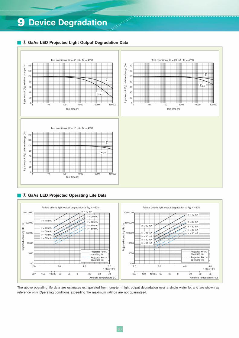
Test time (h)
Test conditions: IF = 50 mA, Ta = 40°C
Ligh
t ou
tput
(P
O)
rela
tive
chan
ge (
%)
Test time (h)
Test conditions: IF = 10 mA, Ta = 40°C
Ligh
t out
put (
PO
) re
lativ
e ch
ange
(%
)
Test time (h)
Test conditions: IF = 20 mA, Ta = 40°C
Ligh
t out
put (
PO
) re
lativ
e ch
ange
(%
)
Failure criteria light output degradation Δ PO < –50%
Pro
ject
ed o
pera
ting
life
(h)
Failure criteria light output degradation Δ PO < –30%
Pro
ject
ed o
pera
ting
life
(h)
10
20
40
60
80
100
120
140
10 100 1000 10000 100000 10
20
40
60
80
100
120
140
10 100 1000 10000 100000
X-3σ
X
10
20
40
60
80
100
120
140
10 100 1000 10000 100000
X-3σ
X
X-3σ
X
2.0 3.0 4.0 5.0100
1000
10000
100000
1000000
10000000
IF = 20 mA
IF = 30 mA
IF = 40 mA
IF = 50 mA
IF = 10 mA
IF = 20 mA
IF = 30 mA
IF = 40 mA
IF = 50 mA
IF = 10 mA
Projected F50% operating life
Projected F0.1% operating life
2.0 3.0 4.0 5.0100
1000
10000
100000
1000000
10000000
IF = 20 mA
IF = 30 mA
IF = 40 mA
IF = 50 mA
IF = 10 mA
IF = 20 mA
IF = 30 mA
IF = 40 mA
IF = 50 mA
IF = 10 mA
Projected F50% operating life
Projected F0.1% operating life
227 150 60 025 –30 –50 –7385100
1 / K (x10-3)
Ambient Temperature (°C) Ambient Temperature (°C)
227 150 60 025 –30 –50 –7385100
1 / K (x10-3)
GaAs LED Projected Light Output Degradation Data1
GaAs LED Projected Operating Life Data1
The above operating life data are estimates extrapolated from long-term light output degradation over a single wafer lot and are shown as
reference only. Operating conditions exceeding the maximum ratings are not guaranteed.
9 Device Degradation
60
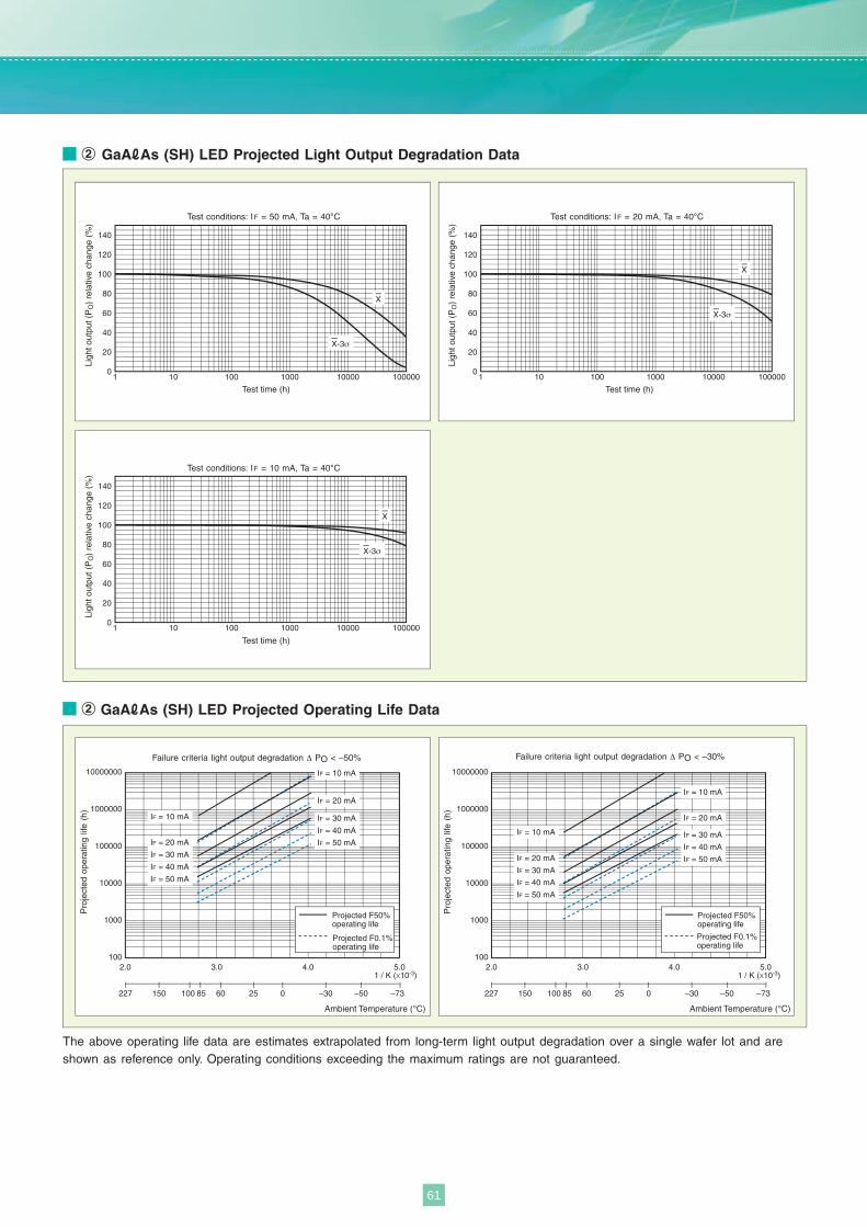
Failure criteria light output degradation Δ PO < –30%
Pro
ject
ed o
pera
ting
life
(h)
Failure criteria light output degradation Δ PO < –50%
Pro
ject
ed o
pera
ting
life
(h)
Test time (h)
Test conditions: IF = 50 mA, Ta = 40°C
Ligh
t out
put (
PO
) re
lativ
e ch
ange
(%
)
Test time (h)
Test conditions: IF = 10 mA, Ta = 40°C
Ligh
t out
put (
PO
) re
lativ
e ch
ange
(%
)
Test time (h)
Test conditions: IF = 20 mA, Ta = 40°C
Ligh
t out
put (
PO
) re
lativ
e ch
ange
(%
)
10
20
40
60
80
100
120
140
10 100 1000 10000 100000
X-3σ
X
10
20
40
60
80
100
120
140
10 100 1000 10000 100000
X-3σ
X
10
20
40
60
80
100
120
140
10 100 1000 10000 100000
X-3σ
X
2.0 3.0 4.0 5.0100
1000
10000
100000
1000000
10000000
IF = 20 mA
IF = 30 mA
IF = 40 mA
IF = 50 mA
IF = 10 mA
IF = 20 mA
IF = 30 mA
IF = 40 mA
IF = 50 mA
IF = 10 mA
Projected F50% operating life
Projected F0.1% operating life
2.0 3.0 4.0 5.0100
1000
10000
100000
1000000
10000000
IF = 20 mA
IF = 30 mA
IF = 40 mA
IF = 50 mA
IF = 10 mA
IF = 20 mA
IF = 30 mA
IF = 40 mA
IF = 50 mA
IF = 10 mA
Projected F50% operating life
Projected F0.1% operating life
227 150 60 025 –30 –50 –7385100
1 / K (x10-3)
227 150 60 025 –30 –50 –7385100
1 / K (x10-3)
Ambient Temperature (°C)Ambient Temperature (°C)
2
2 GaA As (SH) LED Projected Light Output Degradation Data
The above operating life data are estimates extrapolated from long-term light output degradation over a single wafer lot and are shown as reference only. Operating conditions exceeding the maximum ratings are not guaranteed.
GaA As (SH) LED Projected Operating Life Data
61
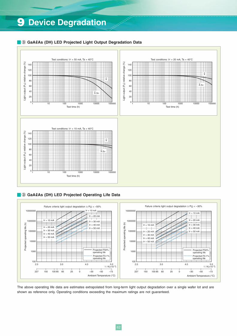
Failure criteria light output degradation Δ PO < –30%
Pro
ject
ed o
pera
ting
life
(h)
Failure criteria light output degradation Δ PO < –50%
Pro
ject
ed o
pera
ting
life
(h)
Test time (h)
Test conditions: IF = 50 mA, Ta = 40°C
Ligh
t out
put (
PO
) re
lativ
e ch
ange
(%
)
Test time (h)
Test conditions: IF = 10 mA, Ta = 40°C
Ligh
t out
put (
PO
) re
lativ
e ch
ange
(%
)
Test time (h)
Test conditions: IF = 20 mA, Ta = 40°C
Ligh
t out
put (
PO
) re
lativ
e ch
ange
(%
)
10
20
40
60
80
100
120
140
10 100 1000 10000 100000
X-3σ
X
10
20
40
60
80
100
120
140
10 100 1000 10000 100000
X-3σ
X
10
20
40
60
80
100
120
140
10 100 1000 10000 100000
X-3σ
X
2.0 3.0 4.0 5.0100
1000
10000
100000
1000000
10000000
IF = 20 mA
IF = 30 mA
IF = 40 mA
IF = 50 mA
IF = 10 mA
IF = 20 mA
IF = 30 mA
IF = 40 mA
IF = 50 mA
IF = 10 mA
Projected F50% operating life
Projected F0.1% operating life
2.0 3.0 4.0 5.0100
1000
10000
100000
1000000
10000000
IF = 20 mA
IF = 30 mA
IF = 40 mA
IF = 50 mA
IF = 10 mA
IF = 20 mA
IF = 30 mA
IF = 40 mA
IF = 50 mA
IF = 10 mA
Projected F50% operating life
Projected F0.1% operating life
227 150 60 025 –30 –50 –7385100
1 / K(×10−3)
Ambient Temperature (°C)
227 150 60 025 –30 –50 –7385100
1 / K(×10−3)
Ambient Temperature (°C)
The above operating life data are estimates extrapolated from long-term light output degradation over a single wafer lot and are shown as reference only. Operating conditions exceeding the maximum ratings are not guaranteed.
GaA As (DH) LED Projected Light Output Degradation Data3
GaA As (DH) LED Projected Operating Life Data3
9 Device Degradation
62
N o t e
Toshiba is now preparing the light output degradation and operating life data for GaA As LEDs. These data are available for individual LEDs. Ask your local Toshiba sales representative.
GaA As (MQW) LED Projected Light Output Degradation and Operating Life Data4
63
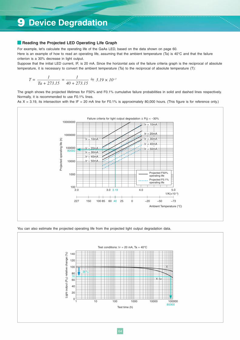
227 150 100 85 60 40 25 0 −20 −50 −73
2.0
1 10
140
120
100
807060
40
20
0100 1000 10000 100000
80000
3.0 4.03.19 5.0
Ambient Temperature (°C)
Test time (h)
Failure criteria for light output degradation Δ PO < –30%
Test conditions: IF = 20 mA, Ta = 40°C
Pro
ject
ed o
pera
ting
life
(h)
Ligh
t out
put (
PO
) re
lativ
e ch
ange
(%
)
Projected F50% operating life
IF = 10mA
IF = 20mA
IF = 30mA
IF = 40mA
IF = 50mA
IF = 10mA
IF = 20mAIF = 30mA
IF = 40mA
IF = 50mA
Projected F0.1% operating life
1/K(×10–3)
10000000
1000000
10000080000
10000
1000
100
–30%
X-3σ
X
Reading the Projected LED Operating Life GraphFor example, let's calculate the operating life of the GaAs LED, based on the data shown on page 60.Here is an example of how to read an operating life, assuming that the ambient temperature (Ta) is 40°C and that the failure criterion is a 30% decrease in light output.Suppose that the initial LED current, IF, is 20 mA. Since the horizontal axis of the failure criteria graph is the reciprocal of absolute temperature, it is necessary to convert the ambient temperature (Ta) to the reciprocal of absolute temperature (T):
The graph shows the projected lifetimes for F50% and F0.1% cumulative failure probabilities in solid and dashed lines respectively. Normally, it is recommended to use F0.1% lines.As X = 3.19, its intersection with the IF = 20 mA line for F0.1% is approximately 80,000 hours. (This figure is for reference only.)
You can also estimate the projected operating life from the projected light output degradation data.
T = =1Ta + 273.15
140 + 273.15
3.19 × 10⁻³
9 Device Degradation
64
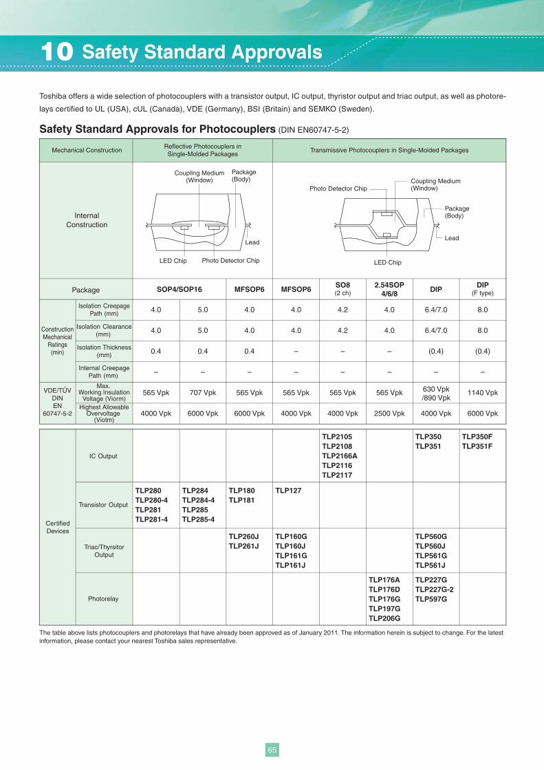
Coupling Medium(Window)
Photo Detector ChipLED Chip
Lead
Package(Body) Coupling Medium
(Window)Photo Detector Chip
LED Chip
Lead
Package(Body)
Transmissive Photocouplers in Single-Molded PackagesReflective Photocouplers inSingle-Molded Packages
Mechanical Construction
4.0 4.0 4.0 4.2 4.0 6.4/7.0 8.05.0
4.0 4.0 4.0 4.2 4.0 6.4/7.0 8.05.0
0.4 0.4 – – – (0.4) (0.4)0.4
– – – – – – ––
565 Vpk
4000 Vpk
707 Vpk
6000 Vpk
565 Vpk
6000 Vpk
565 Vpk
4000 Vpk
565 Vpk
4000 Vpk
565 Vpk
2500 Vpk
630 Vpk/890 Vpk
4000 Vpk
1140 Vpk
6000 Vpk
SOP4/SOP16 MFSOP6 MFSOP6 DIPSO8(2 ch)
2.54SOP4/6/8
DIP(F type)
ConstructionMechanical
Ratings(min)
VDE/TÜVDINEN
60747-5-2
Isolation CreepagePath (mm)
IC Output
Transistor Output
Triac/ThyrsitorOutput
Photorelay
CertifiedDevices
Isolation Clearance(mm)
Isolation Thickness(mm)
Internal CreepagePath (mm)
Max. Working Insulation
Voltage (Viorm)Highest Allowable
Overvoltage (Viotm)
InternalConstruction
Package
TLP280TLP280-4TLP281TLP281-4
TLP284TLP284-4TLP285TLP285-4
TLP180TLP181
TLP260JTLP261J
TLP127
TLP560GTLP560JTLP561GTLP561J
TLP160GTLP160JTLP161GTLP161J
TLP176ATLP176DTLP176GTLP197GTLP206G
TLP227GTLP227G-2TLP597G
TLP2105TLP2108TLP2166ATLP2116TLP2117
TLP350TLP351
TLP350FTLP351F
Safety Standard Approvals for Photocouplers (DIN EN60747-5-2)
Toshiba offers a wide selection of photocouplers with a transistor output, IC output, thyristor output and triac output, as well as photore-
lays certified to UL (USA), cUL (Canada), VDE (Germany), BSI (Britain) and SEMKO (Sweden).
The table above lists photocouplers and photorelays that have already been approved as of January 2011. The information herein is subject to change. For the latest information, please contact your nearest Toshiba sales representative.
10 Safety Standard Approvals
65
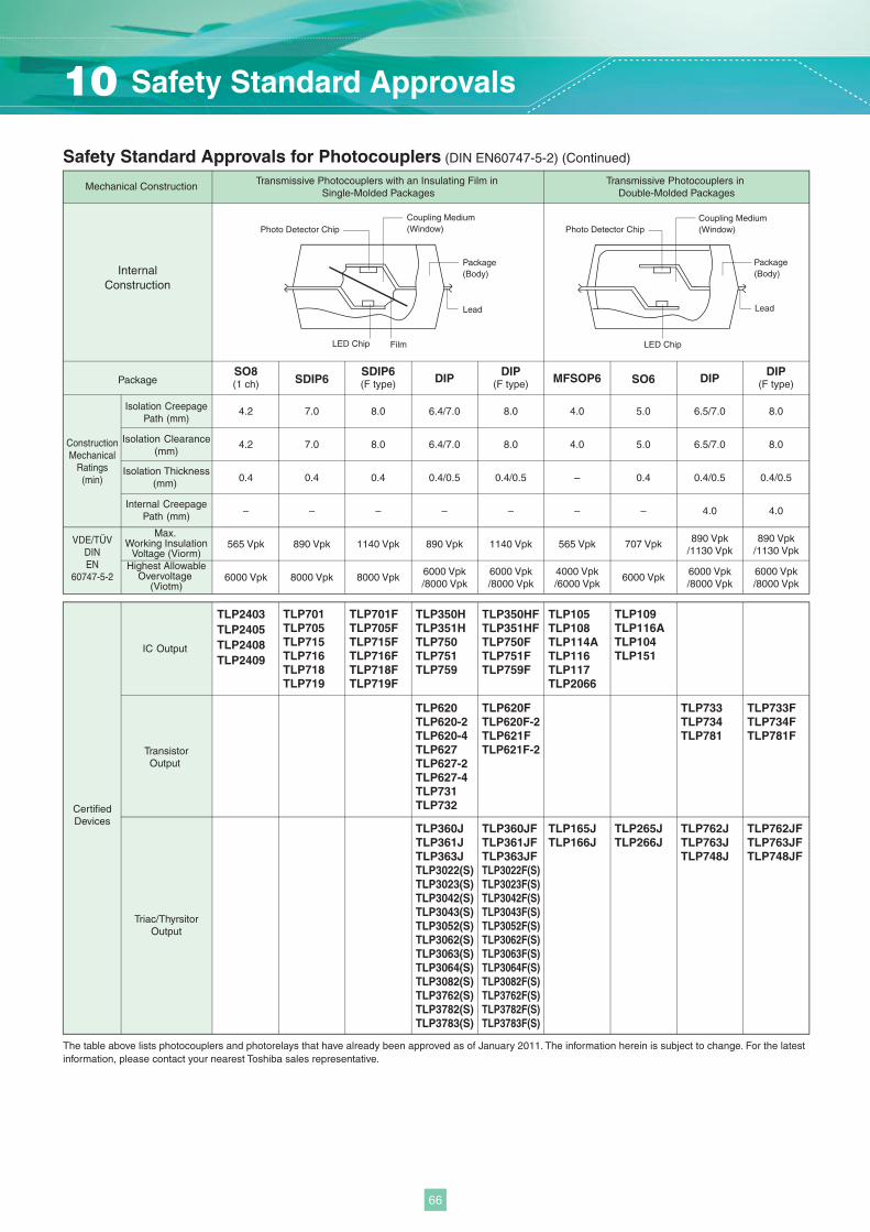
Coupling Medium(Window)Photo Detector Chip
LED Chip
Lead
Package(Body)
Coupling Medium(Window)Photo Detector Chip
LED Chip Film
Lead
Package(Body)
TLP620TLP620-2TLP620-4TLP627TLP627-2TLP627-4TLP731TLP732
TLP620FTLP620F-2TLP621FTLP621F-2
TLP360JTLP361JTLP363JTLP3022(S)TLP3023(S)TLP3042(S)TLP3043(S)TLP3052(S)TLP3062(S)TLP3063(S)TLP3064(S)TLP3082(S)TLP3762(S)TLP3782(S)TLP3783(S)
TLP360JFTLP361JFTLP363JFTLP3022F(S)TLP3023F(S)TLP3042F(S)TLP3043F(S)TLP3052F(S)TLP3062F(S)TLP3063F(S)TLP3064F(S)TLP3082F(S)TLP3762F(S)TLP3782F(S)TLP3783F(S)
TLP733TLP734TLP781
TLP165JTLP166J
TLP733FTLP734FTLP781F
TLP265JTLP266J
TLP762JTLP763JTLP748J
TLP762JFTLP763JFTLP748JF
Transmissive Photocouplers in Double-Molded Packages
Transmissive Photocouplers with an Insulating Film in Single-Molded Packages
7.0 8.0 4.0 5.0 8.08.0
7.0 8.0 4.0 5.0 8.08.0
0.4 0.4/0.5 – 0.4
6.4/7.0
6.4/7.0
0.4/0.5
6.5/7.0
6.5/7.0
0.4/0.5 0.4/0.50.4
– – – – – 4.0 4.0–
890 Vpk
8000 Vpk
1140 Vpk
8000 Vpk
890 Vpk 1140 Vpk 565 Vpk 707 Vpk
6000 Vpk
890 Vpk/1130 Vpk
890 Vpk/1130 Vpk
6000 Vpk/8000 Vpk
6000 Vpk/8000 Vpk
4000 Vpk/6000 Vpk
6000 Vpk/8000 Vpk
6000 Vpk/8000 Vpk
DIP MFSOP6 DIPSDIP6SDIP6(F type)
DIP(F type) SO6
DIP(F type)
ConstructionMechanical
Ratings(min)
VDE/TÜVDINEN
60747-5-2
Isolation CreepagePath (mm)
IC Output
TransistorOutput
Triac/ThyrsitorOutput
CertifiedDevices
Isolation Clearance(mm)
Isolation Thickness(mm)
Internal CreepagePath (mm)
Max. Working Insulation
Voltage (Viorm)Highest Allowable
Overvoltage (Viotm)
InternalConstruction
Package
TLP105TLP108TLP114ATLP116TLP117TLP2066
TLP350HFTLP351HFTLP750FTLP751FTLP759F
TLP350HTLP351HTLP750TLP751TLP759
TLP701FTLP705FTLP715FTLP716FTLP718FTLP719F
TLP701TLP705TLP715TLP716TLP718TLP719
TLP109TLP116ATLP104TLP151
The table above lists photocouplers and photorelays that have already been approved as of January 2011. The information herein is subject to change. For the latest information, please contact your nearest Toshiba sales representative.
Safety Standard Approvals for Photocouplers (DIN EN60747-5-2) (Continued)
Mechanical Construction
4.2
4.2
0.4
–
565 Vpk
6000 Vpk
SO8(1 ch)
TLP2403TLP2405TLP2408TLP2409
10 Safety Standard Approvals
66
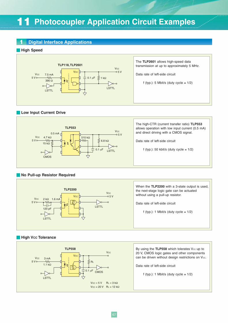
VCC
VCC
LSTTL
0.1 μF
LSTTL
5 VVCC
5 V7.5 mA
390 Ω1 kΩ
TLP118, TLP2601
VCC
VCC
LSTTL
LSTTL
5 VVCC
5 V2 kΩ 1.6 mA
120 pF
TLP2200
5 V
VCC
RL
VCC
VCC = 5 V RL = 3 kΩ
VCC = 20 V RL = 12 kΩ
CMOS
VCC 3 mA
1.1 kΩ
0.1 μF
LSTTL
TLP558
VCC
LSTTL0.1 μF
CMOS
5 VVCC
5 V4.7 kΩ
0.5 mA
15 kΩ6.8 kΩ
510 kΩ
TLP553
1
The TLP2601 allows high-speed data transmission at up to approximately 5 MHz.
Data rate of left-side circuit
f (typ.): 5 Mbit/s (duty cycle ≅ 1/2)
No Pull-up Resistor Required
When the TLP2200 with a 3-state output is used, the next-stage logic gate can be actuated without using a pull-up resistor.
Data rate of left-side circuit
f (typ.): 1 Mbit/s (duty cycle ≅ 1/2)
By using the TLP558 which tolerates VCC up to 20 V, CMOS logic gates and other components can be driven without design restrictions on VCC.
Data rate of left-side circuit
f (typ.): 1 Mbit/s (duty cycle ≅ 1/2)
Digital Interface Applications
The high-CTR (current transfer ratio) TLP553allows operation with low input current (0.5 mA) and direct driving with a CMOS signal.
Data rate of left-side circuit
f (typ.): 50 kbit/s (duty cycle ≅ 1/2)
Low Input Current Drive
High Speed
High VCC Tolerance
11 Photocoupler Application Circuit Examples
67
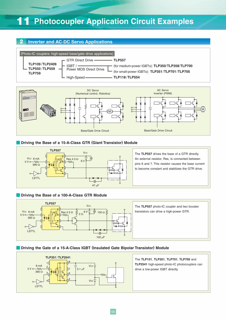
MM
Base/Gate Drive Circuit
DC Servo(Numerical control, Robotics)
Base/Gate Drive Circuit
AC ServoInverter (PWM)
TLP557VCC
47 μF
LSTTL
6 VVCC
5 V8 mA
390 Ω
Rex 4.3 Ω
TLP557VCC
100 μF
LSTTL
8 VVCC
5 V8 mA
390 Ω
Rex 4.3 Ω2 Ω
150 Ω
TLP351 / TLP2541
VCC
VEE
LSTTL
0.1 μF5 V8 mA
12
3
45
6
7
8
390 Ω
2
TLP557
(for medium-power IGBTs): TLP350/ TLP358/ TLP700
(for small-power IGBTs): TLP351 / TLP701 / TLP705
TLP118 / TLP554
GTR Direct Drive
IGBT / Power MOS Direct Drive
High-Speed
TLP109 / TLP2409TLP550 / TLP559TLP759
The TLP557 drives the base of a GTR directly.
An external resistor, Rex, is connected between
pins 6 and 7. This resistor causes the base current
to become constant and stabilizes the GTR drive.
The TLP557 photo-IC coupler and two booster
transistors can drive a high-power GTR.
The TLP151, TLP351, TLP701, TLP705 and
TLP2541 high-speed photo-IC photocouplers can
drive a low-power IGBT directly.
[Photo-IC couplers: high-speed base/gate drive applications]
Inverter and AC-DC Servo Applications
Driving the Base of a 15-A-Class GTR (Giant Transistor) Module
Driving the Base of a 100-A-Class GTR Module
Driving the Gate of a 15-A-Class IGBT (Insulated Gate Bipolar Transistor) Module
11 Photocoupler Application Circuit Examples
68
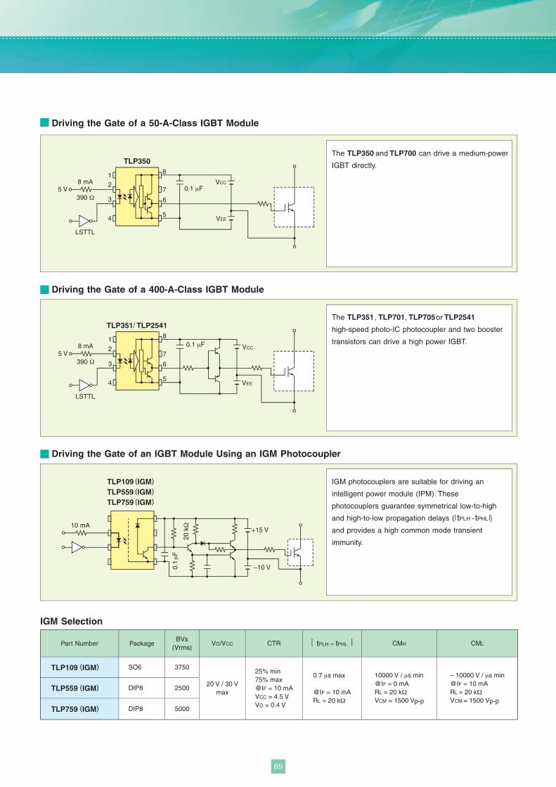
TLP109 (IGM)
TLP559 (IGM)
TLP759 (IGM)
10 mA
0.1μ
F
20 kΩ
+15 V
–10 V
TLP351/ TLP2541
VCC
VEE
LSTTL
0.1 μF5 V
8 mA12
3
45
6
7
8
390 Ω
TLP350
VCC
VEE
LSTTL
0.1 μF5 V8 mA
12
3
45
6
7
8
390 Ω
IGM Selection
20 V / 30 Vmax
25% min75% max@IF = 10 mAVCC = 4.5 VVO = 0.4 V
0.7 μs max
@IF = 10 mARL = 20 kΩ
10000 V / μs min@IF = 0 mARL = 20 kΩVCM = 1500 Vp-p
– 10000 V / μs min@IF = 10 mARL = 20 kΩVCM = 1500 Vp-p
Part Number PackageBVs
(Vrms)VO/VCC CTR CMH CMLtPLH – tPHL
TLP559 (IGM)
TLP759 (IGM)
SO6TLP109 (IGM) 3750
DIP8 2500
DIP8 5000
Driving the Gate of an IGBT Module Using an IGM Photocoupler
IGM photocouplers are suitable for driving an
intelligent power module (IPM). These
photocouplers guarantee symmetrical low-to-high
and high-to-low propagation delays (l tPLH - tPHLl)
and provides a high common mode transient
immunity.
The TLP351 , TLP701, TLP705or TLP2541
high-speed photo-IC photocoupler and two booster
transistors can drive a high power IGBT.
Driving the Gate of a 400-A-Class IGBT Module
The TLP350 and TLP700 can drive a medium-power
IGBT directly.
Driving the Gate of a 50-A-Class IGBT Module
69
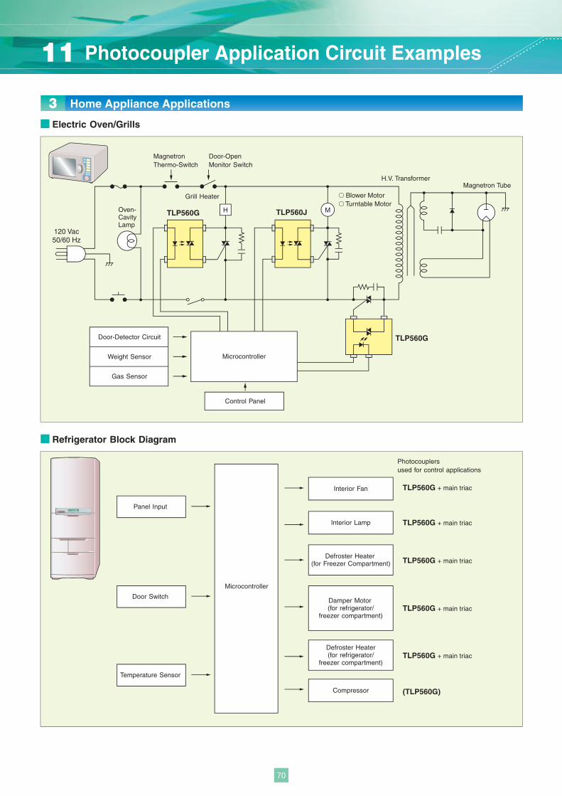
TLP560G + main triac
TLP560G + main triac
TLP560G + main triac
TLP560G + main triac
TLP560G + main triac
(TLP560G)
Panel Input
Microcontroller
Door Switch
Temperature Sensor
Compressor
Defroster Heater(for refrigerator/
freezer compartment)
Damper Motor (for refrigerator/
freezer compartment)
Defroster Heater (for Freezer Compartment)
Interior Lamp
Interior Fan
Photocouplersused for control applications
HTLP560G
TLP560G
TLP560J M
120 Vac50/60 Hz
Oven-CavityLamp
MagnetronThermo-Switch
Door-OpenMonitor Switch
H.V. TransformerMagnetron Tube
Blower MotorTurntable Motor
Grill Heater
Weight Sensor
Door-Detector Circuit
Gas Sensor
Microcontroller
Control Panel
Electric Oven/Grills
Refrigerator Block Diagram
Home Appliance Applications3
11 Photocoupler Application Circuit Examples
70
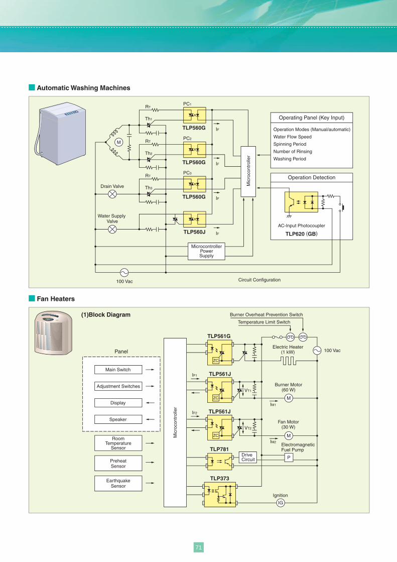
(1)Block Diagram
Main Switch
Adjustment Switches
Display
Speaker
M
TLP560G
RT
IF
PC1
Th1
TLP560G
RT
IF
PC2
Th2
TLP560G
RT
IF
PC3
Th3
TLP560J IF
AC-Input Photocoupler
TLP620 (GB)
100 Vac
Drain Valve
Water Supply Valve
MicrocontrollerPowerSupply
Operating Panel (Key Input)
Operation Detection
Operation Modes (Manual/automatic)
Water Flow Speed
Spinning Period
Number of Rinsing
Washing Period
Circuit Configuration
Mic
roco
ntro
ller
100 Vac
P
M
TLP561G
ZC
ZC
ZC
IF1
VT1
TLP561J
IM1
M
IF2
VT2
TLP561J
IG
TLP781
TLP373
IM2
Panel
Temperature Limit Switch
Burner Overheat Prevention Switch
DriveCircuit
RoomTemperature
Sensor
PreheatSensor
EarthquakeSensor
Ignition
Burner Motor(60 W)
Electric Heater(1 kW)
Fan Motor(30 W)
ElectromagneticFuel Pump
Mic
roco
ntro
ller
Automatic Washing Machines
Fan Heaters
71
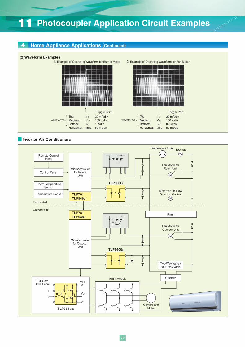
Trigger Point
Top: IF1 20 mA/divMedium: VT1 100 V/divBottom: IM1 1 A/divHorizontal: time 50 ms/div
Top: IF2 20 mA/divMedium: VT2 100 V/divBottom: IM2 0.5 A/divHorizontal: time 50 ms/div
Trigger Point
1. Example of Operating Waveform for Burner Motor 2. Example of Operating Waveform for Fan Motor
TLP560G
M
M
100 Vac
TLP781TLP548J
TLP560G
TLP351 x 6
M
TLP781TLP548J
VCC
VO
ZC
Fan Motor forRoom Unit
Motor for Air-FlowDirection Control
Control Panel
Remote ControlPanel
Room TemperatureSensor
Temperature Sensor
Indoor Unit
Outdoor Unit
Fan Motor forOutdoor Unit
Temperature Fuse
Rectifier
CompressorMotor
IGBT ModuleIGBT GateDrive Circuit
Two-Way Valve /Four-Way Valve
Filter
Microcontrollerfor Indoor
Unit
Microcontrollerfor Outdoor
Unit
waveforms waveforms
(2)Waveform Examples
Inverter Air Conditioners
4 Home Appliance Applications (Continued)
11 Photocoupler Application Circuit Examples
72
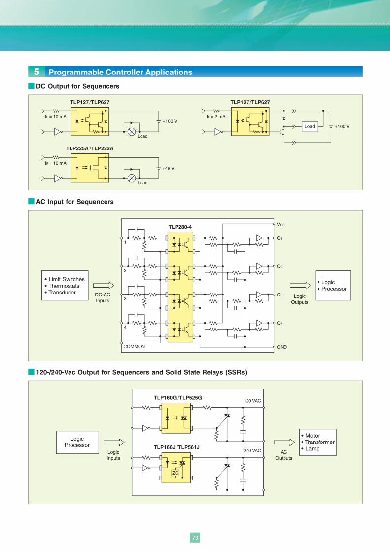
+100 V
Load
IF = 10 mA
TLP127 /TLP627
+100 VLoad
IF = 2 mA
TLP127 /TLP627
+48 V
Load
IF = 10 mA
TLP225A /TLP222A
ACOutputs
LogicInputs
LogicProcessor
● Motor● Transformer● Lamp
TLP160G /TLP525G
TLP166J /TLP561J
ZC
240 VAC
120 VAC
● Limit Switches● Thermostats● Transducer
● Logic ● Processor
1O1
VCCTLP280-4
2O2
3O3
4O4
GNDCOMMON
DC-ACInputs
LogicOutputs
DC Output for Sequencers
Programmable Controller Applications
120-/240-Vac Output for Sequencers and Solid State Relays (SSRs)
AC Input for Sequencers
5
73
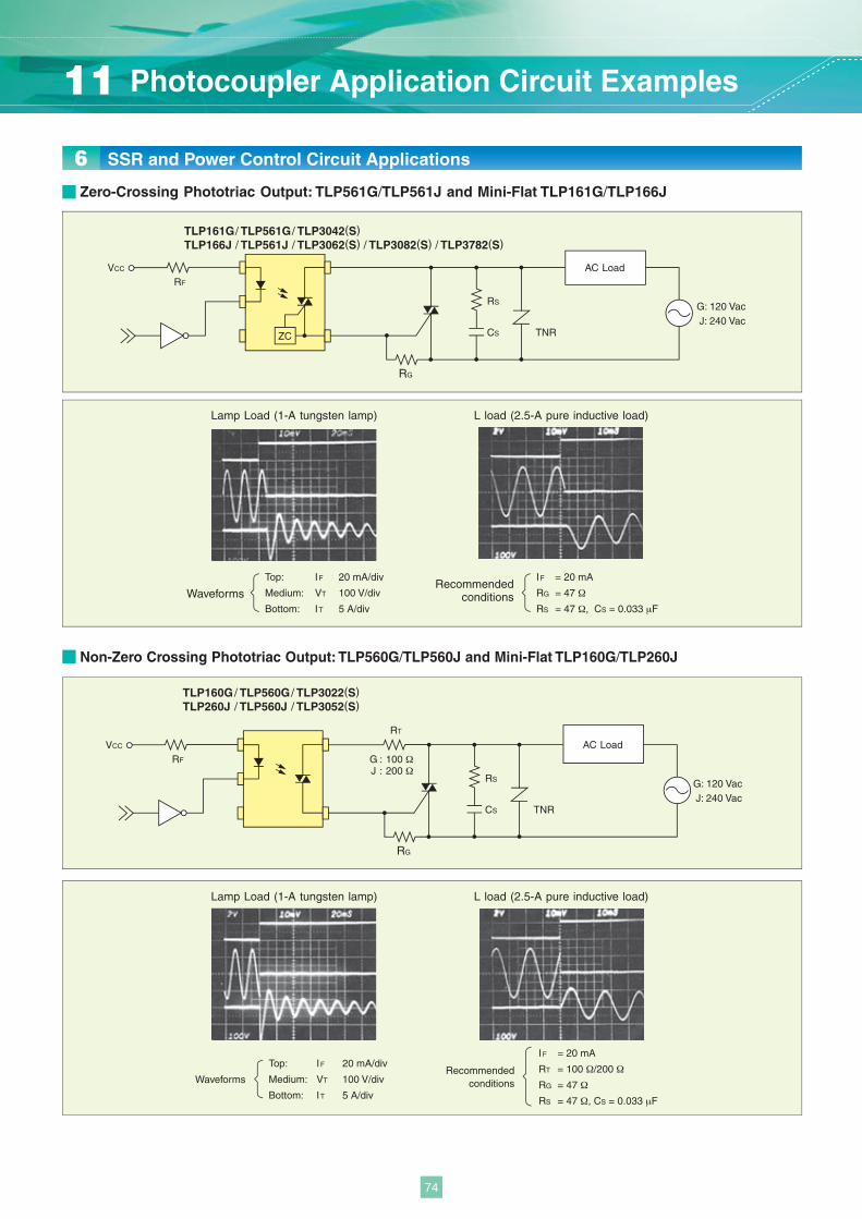
RS
RG
RF
VCC
CS TNR
AC Load
ZC
G: 120 VacJ: 240 Vac
Lamp Load (1-A tungsten lamp) L load (2.5-A pure inductive load)
Lamp Load (1-A tungsten lamp) L load (2.5-A pure inductive load)
TLP161G/ TLP561G / TLP3042(S)TLP166J / TLP561J / TLP3062(S) / TLP3082(S) / TLP3782(S)
Top: IF 20 mA/div
Medium: VT 100 V/div
Bottom: IT 5 A/div
Waveforms
Top: IF 20 mA/div
Medium: VT 100 V/div
Bottom: IT 5 A/div
Waveforms
IF = 20 mA
RG = 47 Ω
RS = 47 Ω, CS = 0.033 μF
IF = 20 mA
RT = 100 Ω/200 Ω
RG = 47 Ω
RS = 47 Ω, CS = 0.033 μF
Recommendedconditions
Recommendedconditions
TLP160G / TLP560G / TLP3022(S)TLP260J / TLP560J / TLP3052(S)
RS
RG
RF
RT
G : 100 Ω J : 200 Ω
VCC
CS TNR
AC Load
G: 120 VacJ: 240 Vac
SSR and Power Control Circuit Applications6Zero-Crossing Phototriac Output: TLP561G/TLP561J and Mini-Flat TLP161G/TLP166J
Non-Zero Crossing Phototriac Output: TLP560G/TLP560J and Mini-Flat TLP160G/TLP260J
11 Photocoupler Application Circuit Examples
74
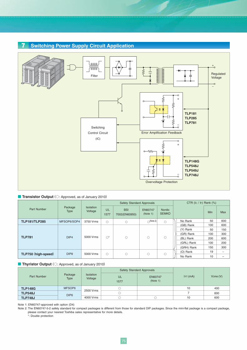
TLP181TLP285TLP781
TLP148GTLP548JTLP549JTLP748J
Filter
Switching
Control Circuit
(IC)
RegulatedVoltage
Error Amplification Feedback
−
−
−
+
+
+
Overvoltage Protection
7 Switching Power Supply Circuit Application
■ Transistor Output ( : Approved, as of January 2010)
■ Thyristor Output ( : Approved, as of January 2010)
Note 1: EN60747-approved with option (D4)Note 2: The EN60747-5-2 safety standard for compact packages is different from those for standard DIP packages. Since the mini-flat package is a compact package,
please contact your nearest Toshiba sales representative for more details.*: Double protection
Safety Standard Approvals CTR (IC / IF) Rank (%)
PackageType UL
1577
EN60747(Note 1)
NordicSEMKO
BSI
7002(EN60950)
Part NumberMin Max
IsolationVoltage
PackageType UL
1577
EN60747(Note 1)
Safety Standard Approvals
Part NumberIsolationVoltage
IFT (mA) VDRM (V)
No Rank(GB) Rank
(Y) Rank
(GR) Rank
(BL) Rank
(GRL) Rank
(GRH) Rank
No Rank
(O) Rank
TLP181/TLP285
TLP781
TLP750 (high-speed)
MFSOP6/SOP4
DIP4
DIP8
*
(Note 2) 50100
50
100
200
100
150
19
10
600600
150
300
600
200
300
–
–
DIP6
TLP148GTLP548JTLP748J
MFSOP6
3750 Vrms
5000 Vrms
5000 Vrms
2500 Vrms
4000 Vrms
10
7
10 600
600
400
75
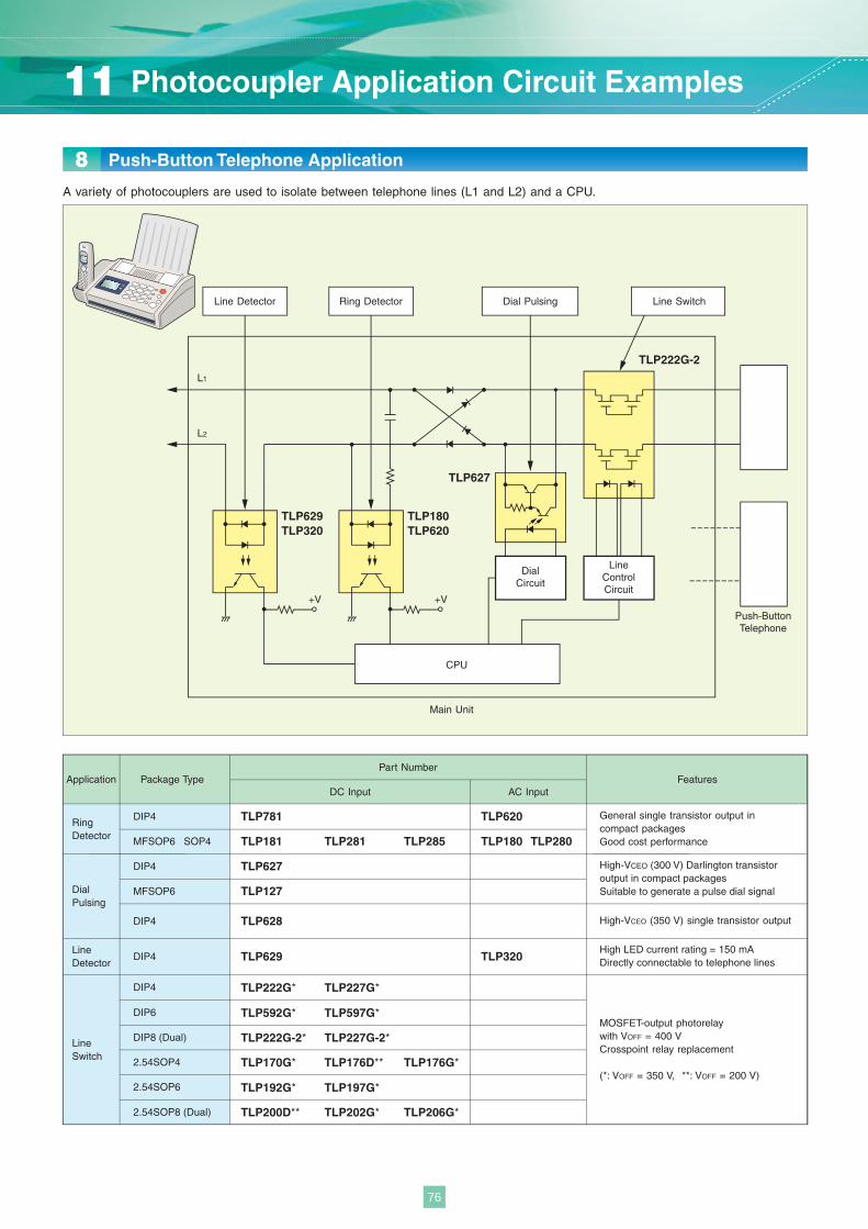
TLP180TLP620
TLP222G-2
CPU
L1
L2
+V
TLP629TLP320
+V
TLP627
Dial PulsingRing Detector Line SwitchLine Detector
Push-ButtonTelephone
LineControlCircuit
DialCircuit
Main Unit
Push-Button Telephone Application8A variety of photocouplers are used to isolate between telephone lines (L1 and L2) and a CPU.
Application Package Type FeaturesPart Number
DC Input AC Input
General single transistor output in compact packagesGood cost performance
High-VCEO (300 V) Darlington transistor output in compact packagesSuitable to generate a pulse dial signal
MOSFET-output photorelay with VOFF = 400 VCrosspoint relay replacement
(*: VOFF = 350 V, **: VOFF = 200 V)
High LED current rating = 150 mADirectly connectable to telephone lines
High-VCEO (350 V) single transistor output
RingDetector
DialPulsing
LineDetector
LineSwitch
DIP4
MFSOP6 SOP4
DIP4
MFSOP6
DIP4
DIP4
DIP4
DIP6
2.54SOP4
2.54SOP6
TLP781
TLP181 TLP281 TLP285
TLP627
TLP127
TLP628
TLP629
TLP620
TLP180 TLP280
TLP320
TLP222G* TLP227G*
TLP592G* TLP597G*
TLP222G-2* TLP227G-2*
TLP170G* TLP176D** TLP176G*
TLP192G* TLP197G*
TLP200D** TLP202G* TLP206G*
DIP8 (Dual)
2.54SOP8 (Dual)
11 Photocoupler Application Circuit Examples
76
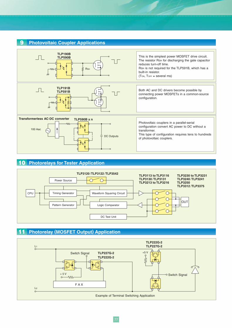
100 Aac
DC Outputs
TLP590B x n
RSH
TLP190BTLP590B
TLP191BTLP591B
TLP222G-2TLP227G-2
TLP227G-2TLP222G-2
L1
L2
Switch Signal
Switch Signal
Example of Terminal Switching Application
+5 V
+ 5 V
F A X
Timing GeneratorCPU
OUT
Waveform Squaring Circuit
Power Source
DC Test Unit
Logic ComparatorPattern Generator
TLP3120 /TLP3122 /TLP3542TLP3113 to TLP3116TLP3130 /TLP3131TLP3213 to TLP3216
TLP3230 to TLP3231TLP3240 /TLP3241TLP3250TLP3312 /TLP3375
Transformerless AC-DC converter
Photovoltaic Coupler Applications
Photorelay (MOSFET Output) Application
Photorelays for Tester Application10
9
11
This is the simplest power MOSFET drive circuit. The resistor RSH for discharging the gate capacitor reduces turn-off time. RSH is not required for the TLP591B, which has a built-in resistor.(TON, TOFF ≅ several ms)
Both AC and DC drivers become possible by connecting power MOSFETs in a common-source configuration.
Photovoltaic couplers in a parallel-serial configuration convert AC power to DC without a transformer. This type of configuration requires tens to hundreds of photovoltaic couplers.
77
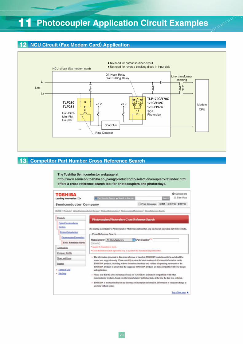
TLP280TLP281
TLP172G/170G176G/192G176D/197GSOPPhotorelay
Off-Hook RelayDial Pulsing Relay
● No need for output snubber circuit● No need for reverse-blocking diode in input side
NCU circuit (fax modem card)
Half-PitchMini-FlatCoupler
Line transformershorting
+5 V +5 V
Line
Modem
CPU
Controller
Ring Detector
L1
L2
NCU Circuit (Fax Modem Card) Application
Competitor Part Number Cross Reference Search
12
13
The Toshiba Semiconductor webpage at http://www.semicon.toshiba.co.jp/eng/product/opto/selection/coupler/xref/index.html offers a cross reference search tool for photocouplers and photorelays.
11 Photocoupler Application Circuit Examples
78
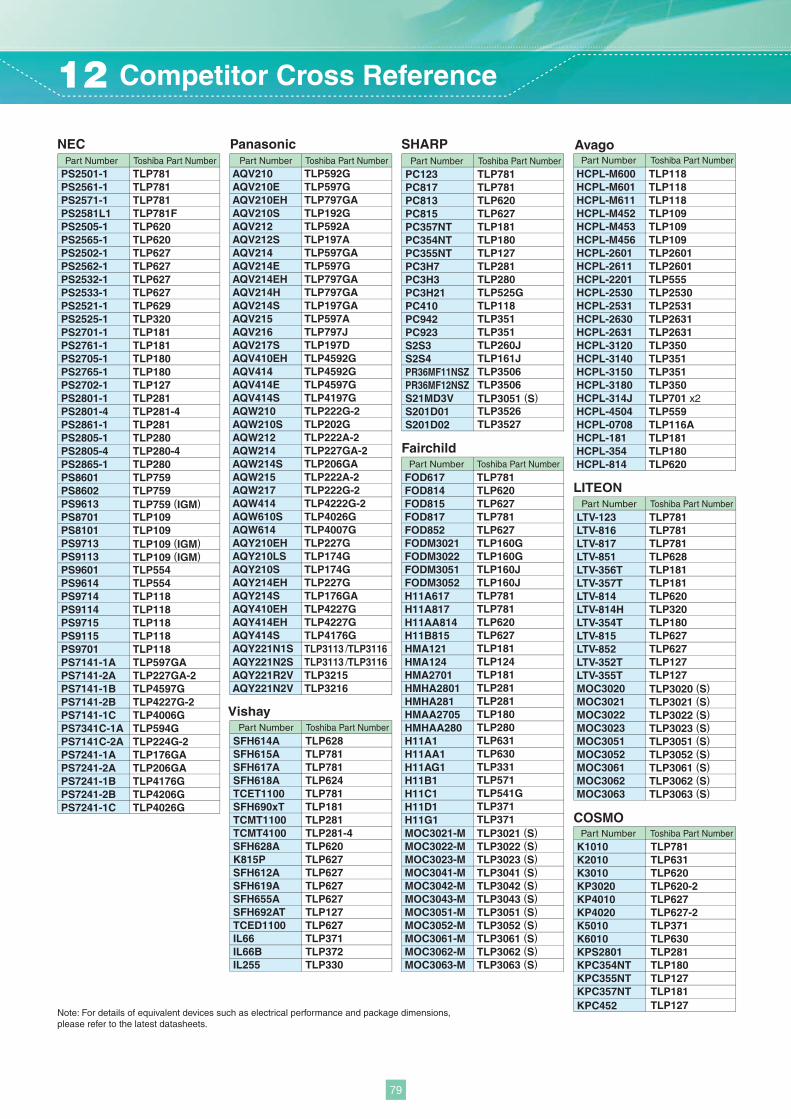
Note: For details of equivalent devices such as electrical performance and package dimensions, please refer to the latest datasheets.
AvagoSHARPPanasonicNEC
COSMO
K1010K2010K3010KP3020KP4010KP4020K5010K6010KPS2801KPC354NTKPC355NTKPC357NTKPC452
TLP781TLP631TLP620TLP620-2TLP627TLP627-2TLP371TLP630TLP281TLP180TLP127TLP181TLP127
HCPL-M600HCPL-M601HCPL-M611HCPL-M452HCPL-M453HCPL-M456HCPL-2601HCPL-2611HCPL-2201HCPL-2530HCPL-2531HCPL-2630HCPL-2631HCPL-3120HCPL-3140HCPL-3150HCPL-3180HCPL-314JHCPL-4504HCPL-0708HCPL-181HCPL-354HCPL-814
TLP118TLP118TLP118TLP109TLP109TLP109TLP2601TLP2601TLP555TLP2530TLP2531TLP2631TLP2631TLP350TLP351TLP351TLP350TLP701 x2TLP559TLP116ATLP181TLP180TLP620
Vishay
SFH614ASFH615ASFH617ASFH618ATCET1100SFH690xTTCMT1100TCMT4100SFH628AK815PSFH612ASFH619A
TLP628TLP781TLP781TLP624TLP781TLP181TLP281TLP281-4TLP620TLP627TLP627TLP627
SFH655A TLP627SFH692AT TLP127TCED1100 TLP627IL66 TLP371IL66B TLP372IL255 TLP330
Fairchild
H11A617H11A817H11AA814H11B815HMA121HMA124HMA2701HMHA2801HMHA281HMAA2705HMHAA280H11A1H11AA1H11AG1H11B1H11C1H11D1H11G1MOC3021-MMOC3022-MMOC3023-MMOC3041-MMOC3042-MMOC3043-MMOC3051-MMOC3052-MMOC3061-MMOC3062-MMOC3063-M
TLP781
FOD617 TLP781FOD814 TLP620FOD815 TLP627FOD817 TLP781FOD852 TLP627FODM3021 TLP160GFODM3022 TLP160GFODM3051 TLP160JFODM3052 TLP160J
TLP781TLP620TLP627TLP181TLP124TLP181TLP281TLP281TLP180TLP280TLP631TLP630TLP331TLP571TLP541GTLP371TLP371TLP3021 (S)TLP3022 (S)TLP3023 (S)TLP3041 (S)TLP3042 (S)TLP3043 (S)TLP3051 (S)TLP3052 (S)TLP3061 (S)TLP3062 (S)TLP3063 (S)
LITEON
LTV-123LTV-816LTV-817LTV-851LTV-356TLTV-357TLTV-814LTV-814HLTV-354TLTV-815LTV-852LTV-352TLTV-355TMOC3020
TLP781TLP781TLP781TLP628TLP181TLP181TLP620TLP320TLP180TLP627TLP627TLP127TLP127
MOC3021MOC3022MOC3023MOC3051MOC3052MOC3061MOC3062MOC3063
TLP3020 (S)TLP3021 (S)TLP3022 (S)TLP3023 (S)TLP3051 (S)TLP3052 (S)TLP3061 (S)TLP3062 (S)TLP3063 (S)
PC123PC817PC813PC815PC357NTPC354NTPC355NTPC3H7PC3H3PC3H21PC410PC942PC923S2S3
TLP781TLP781TLP620TLP627TLP181TLP180TLP127TLP281TLP280TLP525GTLP118TLP351TLP351TLP260J
S2S4 TLP161JPR36MF11NSZ TLP3506PR36MF12NSZ TLP3506S21MD3V TLP3051 (S)S201D01 TLP3526S201D02 TLP3527
AQV210AQV210EAQV210EHAQV210SAQV212AQV212SAQV214AQV214EAQV214EHAQV214HAQV214SAQV215AQV216AQV217SAQV410EHAQV414AQV414EAQV414SAQW210AQW210SAQW212
AQW214SAQW214
AQW215
TLP592GTLP597GTLP797GATLP192GTLP592ATLP197ATLP597GATLP597GTLP797GATLP797GATLP197GATLP597ATLP797JTLP197DTLP4592GTLP4592GTLP4597GTLP4197GTLP222G-2TLP202GTLP222A-2TLP227GA-2TLP206GA
AQW217TLP222A-2TLP222G-2
AQW414 TLP4222G-2AQW610S TLP4026GAQW614 TLP4007GAQY210EH TLP227GAQY210LS TLP174GAQY210S TLP174GAQY214EH TLP227GAQY214S TLP176GAAQY410EH TLP4227GAQY414EH TLP4227GAQY414S TLP4176GAQY221N1S TLP3113 /TLP3116AQY221N2S TLP3113 /TLP3116AQY221R2V TLP3215AQY221N2V TLP3216
PS2501-1PS2561-1PS2571-1PS2581L1PS2505-1PS2565-1PS2502-1PS2562-1PS2532-1PS2533-1PS2521-1PS2525-1PS2701-1PS2761-1PS2705-1PS2765-1PS2702-1PS2801-1PS2801-4PS2861-1PS2805-1PS2805-4PS2865-1PS8601PS8602PS9613PS8701
TLP781TLP781TLP781TLP781FTLP620TLP620TLP627TLP627TLP627TLP627TLP629TLP320TLP181TLP181TLP180TLP180TLP127TLP281TLP281-4TLP281TLP280TLP280-4TLP280TLP759TLP759TLP759 (IGM)TLP109
PS8101 TLP109PS9713 TLP109 (IGM)PS9113 TLP109 (IGM)PS9601 TLP554PS9614 TLP554PS9714 TLP118PS9114 TLP118PS9715 TLP118PS9115 TLP118PS9701 TLP118PS7141-1A TLP597GAPS7141-2A TLP227GA-2PS7141-1B TLP4597GPS7141-2B TLP4227G-2PS7141-1C TLP4006GPS7341C-1A TLP594GPS7141C-2A TLP224G-2PS7241-1A TLP176GAPS7241-2A TLP206GAPS7241-1B TLP4176GPS7241-2B TLP4206GPS7241-1C TLP4026G
Part Number Toshiba Part Number
Part Number Toshiba Part Number
Part Number Toshiba Part Number
Part Number Toshiba Part Number
Part Number Toshiba Part Number
Part Number Toshiba Part NumberPart Number Toshiba Part NumberPart Number Toshiba Part Number
12 Competitor Cross Reference
79
Website: http://www.semicon.toshiba.co.jp/engSemiconductor Company
BCE0034G
Photocouplers and P
hotorelays
Previous edition: BCE0034F2011-3(5k)SO-DQ
2011
OVERSEAS SUBSIDIARIES AND AFFILIATES
Toshiba AmericaElectronic Components, Inc.• Irvine, Headquarters Tel: (949)623-2900 Fax: (949)474-1330
• Buffalo Grove (Chicago) Tel: (847)484-2400 Fax: (847)541-7287
• Duluth/Atlanta Tel: (770)931-3363 Fax: (770)931-7602
• El PasoTel: (915)771-8156
• Marlborough Tel: (508)481-0034 Fax: (508)481-8828
• Parsippany Tel: (973)541-4715 Fax: (973)541-4716
• San Jose Tel: (408)526-2400 Fax: (408)526-2410
• Wixom (Detroit) Tel: (248)347-2607 Fax: (248)347-2602
• Bloomington Tel: (952)842-2400 Fax: (952)893-8031
• San Diego Tel: (858)385-5900 Fax: (858)674-7606
Toshiba Electronics do Brasil Ltda.Tel: (011)2539-6681 Fax: (011)2539-6675
Toshiba Electronics Europe GmbH• Düsseldorf Head Office Tel: (0211)5296-0 Fax: (0211)5296-400
• France Branch Tel: (1)47282181
• Italy Branch Tel: (039)68701 Fax: (039)6870205
• Spain Branch Tel: (91)660-6798 Fax: (91)660-6799
• U.K. Branch Tel: (0870)060-2370 Fax: (01252)53-0250
• Sweden Branch Tel: (08)704-0900 Fax: (08)80-8459
Toshiba Electronics Asia (Singapore) Pte. Ltd.Tel: (6278)5252 Fax: (6271)5155
Toshiba Electronics Service (Thailand) Co., Ltd.Tel: (02)501-1635 Fax: (02)501-1638
Toshiba Electronics Trading (Malaysia) Sdn. Bhd.• Kuala Lumpur Head Office Tel: (03)5631-6311 Fax: (03)5631-6307
• Penang Office Tel: (04)226-8523 Fax: (04)226-8515
Toshiba India Private Ltd.Tel: (0124)499-6600 Fax: (0124)499-6611
Toshiba Electronics Asia, Ltd.• Hong Kong Head Office Tel: 2375-6111 Fax: 2375-0969
• Beijing Office Tel: (010)6590-8796 Fax: (010)6590-8791
• Chengdu Office Tel: (028)8675-1773 Fax: (028)8675-1065
• Qingdao Office Tel: (532)8579-3328 Fax: (532)8579-3329
Toshiba Electronics (Shenzhen) Co.,LtdTel: (0755)2399-6897 Fax: (0755)2399-5573
Toshiba Electronics (Shanghai) Co., Ltd.• Shanghai PUXI Branch Tel: (021)6139-3888 Fax: (021)6190-8288
• Hangzhou Office Tel: (0571)8717-5004 Fax: (0571)8717-5013
• Nanjing Office Tel: (025)8689-0070 Fax: (025)8689-0070
Toshiba Electronics (Dalian) Co., Ltd.Tel: (0411)8368-6882 Fax: (0411)8369-0822
Tsurong Xiamen Xiangyu Trading Co., Ltd.Tel: (0592)226-1398 Fax: (0592)226-1399
Toshiba Electronics Korea Corporation• Seoul Head Office Tel: (02)3484-4334 Fax: (02)3484-4302
• Daegu Office Tel: (053)428-7610 Fax: (053)428-7617
Toshiba Electronics Taiwan Corporation• Taipei Head Office Tel: (02)2508-9988 Fax: (02)2508-9999
2011-3(As of February 14, 2011)
Toshiba Corporation, and its subsidiaries and affiliates (collectively “TOSHIBA”), reserve the right to make changes to the information in this document, and related hardware, software and systems (collectively “Product”) without notice.
This document and any information herein may not be reproduced without prior written permission from TOSHIBA. Even with TOSHIBA’s written permission, reproduction is permissible only if reproduction is without alteration/omission.
Though TOSHIBA works continually to improve Product's quality and reliability, Product can malfunction or fail. Customers are responsible for complying with safety standards and for providing adequate designs and safeguards for their hardware, software and systems which minimize risk and avoid situations in which a malfunction or failure of Product could cause loss of human life, bodily injury or damage to property, including data loss or corruption. Before customers use the Product, create designs including the Product, or incorporate the Product into their own applications, customers must also refer to and comply with (a) the latest versions of all relevant TOSHIBA information, including without limitation, this document, the specifications, the data sheets and application notes for Product and the precautions and conditions set forth in the "TOSHIBA Semiconductor Reliability Handbook" and (b) the instructions for the application with which the Product will be used with or for. Customers are solely responsible for all aspects of their own product design or applications, including but not limited to (a) determining the appropriateness of the use of this Product in such design or applications; (b) evaluating and determining the applicability of any information contained in this document, or in charts, diagrams, programs, algorithms, sample application circuits, or any other referenced documents; and (c) validating all operating parameters for such designs and applications. TOSHIBA ASSUMES NO LIABILITY FOR CUSTOMERS' PRODUCT DESIGN OR APPLICATIONS.
Product is intended for use in general electronics applications (e.g., computers, personal equipment, office equipment, measuring equipment, industrial robots and home electronics appliances) or for specific applications as expressly stated in this document. Product is neither intended nor warranted for use in equipment or systems that require extraordinarily high levels of quality and/or reliability and/or a malfunction or failure of which may cause loss of human life, bodily injury, serious property damage or serious public impact (“Unintended Use”). Unintended Use includes, without limitation, equipment used in nuclear facilities, equipment used in the aerospace industry, medical equipment, equipment used for automobiles, trains, ships and other transportation, traffic signaling equipment, equipment used to control combustions or explosions, safety devices, elevators and escalators, devices related to electric power, and equipment used in finance-related fields. Do not use Product for Unintended Use unless specifically permitted in this document.
Do not disassemble, analyze, reverse-engineer, alter, modify, translate or copy Product, whether in whole or in part.
Product shall not be used for or incorporated into any products or systems whose manufacture, use, or sale is prohibited under any applicable laws or regulations.
The information contained herein is presented only as guidance for Product use. No responsibility is assumed by TOSHIBA for any infringement of patents or any other intellectual property rights of third parties that may result from the use of Product. No license to any intellectual property right is granted by this document, whether express or implied, by estoppel or otherwise.
ABSENT A WRITTEN SIGNED AGREEMENT, EXCEPT AS PROVIDED IN THE RELEVANT TERMS AND CONDITIONS OF SALE FOR PRODUCT, AND TO THE MAXIMUM EXTENT ALLOWABLE BY LAW, TOSHIBA (1) ASSUMES NO LIABILITY WHATSOEVER, INCLUDING WITHOUT LIMITATION, INDIRECT, CONSEQUENTIAL, SPECIAL, OR INCIDENTAL DAMAGES OR LOSS, INCLUDING WITHOUT LIMITATION, LOSS OF PROFITS, LOSS OF OPPORTUNITIES, BUSINESS INTERRUPTION AND LOSS OF DATA, AND (2) DISCLAIMS ANY AND ALL EXPRESS OR IMPLIED WARRANTIES AND CONDITIONS RELATED TO SALE, USE OF PRODUCT, OR INFORMATION, INCLUDING WARRANTIES OR CONDITIONS OF MERCHANTABILITY, FITNESS FOR A PARTICULAR PURPOSE, ACCURACY OF INFORMATION, OR NONINFRINGEMENT.
Product may include products using GaAs (Gallium Arsenide). GaAs is harmful to humans if consumed or absorbed, whether in the form of dust or vapor. Handle with care and do not break, cut, crush, grind, dissolve chemically or otherwise expose GaAs in Product.
Do not use or otherwise make available Product or related software or technology for any military purposes, including without limitation, for the design, development, use, stockpiling or manufacturing of nuclear, chemical, or biological weapons or missile technology products (mass destruction weapons). Product and related software and technology may be controlled under the Japanese Foreign Exchange and Foreign Trade Law and the U.S. Export Administration Regulations. Export and re-export of Product or related software or technology are strictly prohibited except in compliance with all applicable export laws and regulations.
Product may include products subject to foreign exchange and foreign trade control laws.
Please contact your TOSHIBA sales representative for details as to environmental matters such as the RoHS compatibility of Product. Please use Product in compliance with all applicable laws and regulations that regulate the inclusion or use of controlled substances, including without limitation, the EU RoHS Directive. TOSHIBA assumes no liability for damages or losses occurring as a result of noncompliance with applicable laws and regulations.
Mouser Electronics
Authorized Distributor
Click to View Pricing, Inventory, Delivery & Lifecycle Information: Toshiba:
TLP3217(TP15,F) TLP3125(TP,F) TLP558(F) TLP559(F) TLP748J(TP1,F) TLP148G(U,F) TLP114A(TPR,F)
TLP2200(TP1,F) TLP250(TP1,F) TLP251(TP1,F) TLP176A(F) TLP2095(F)


![NOTE: LENGTHS. FOR OTHER LENGTHS CONTACT SAMTEC. · 2017. 10. 11. · sealed overmold: pa66 gf13 fr(70g13l); max regrind: 10%, shot weight: 12.70g [.028lb] non-sealed overmold: pvc;](https://img.pdfslide.net/doc/110x75/60b39d4e8b811c2c356b77ef/note-lengths-for-other-lengths-contact-2017-10-11-sealed-overmold-pa66.jpg)