Embed Size (px)
Citation preview
Photoemission study of the electronic structure and charge density
waves of Na2Ti2Sb2O
S. Y. Tan1,2, J. Jiang2,3, Z. R. Ye2, X. H. Niu2,3, Y. Song4, C. L. Zhang4,5, P. C. Dai4, B. P. Xie2,3,
X. C. Lai1 and D. L. Feng2,3* 1 Science and Technology on Surface Physics and Chemistry Laboratory, Mianyang 621907, China
2Physics Department, Applied Surface Physics State Key Laboratory, and Advanced Materials Laboratory, Fudan
University, Shanghai 200433, China 3Collaborative Innovation Center of Advanced Microstructures, Nanjing University, Nanjing 210093, China
4Department of Physics and Astronomy, Rice University, Houston, Texas 77005, USA 5Department of Physics and Astronomy, The University of Tennessee, Knoxville, Tennessee 37996-1200, USA
*Correspondence and requests for materials should be addressed to D.L.Feng([email protected])
The electronic structure of Na2Ti2Sb2O, a parent compound of the newly discovered
titanium‐based oxypnictide superconductors, is studied by photon energy and polarization
dependent angle‐resolved photoemission spectroscopy (ARPES). The obtained band structure
and Fermi surface agree well with the band structure calculation of Na2Ti2Sb2O in the
non‐magnetic state, which indicating that there is no magnetic order in Na2Ti2Sb2O and the
electronic correlation is weak. Polarization dependent ARPES results suggest the multi‐band
and multi‐orbital nature of Na2Ti2Sb2O. Photon energy dependent ARPES results suggest that
the electronic structure of Na2Ti2Sb2O is rather two‐dimensional. Moreover, we find a density
wave energy gap forms below the transition temperature and reaches 65 meV at 7 K, indicating
that Na2Ti2Sb2O is likely a weakly correlated CDW material in the strong electron‐phonon
interaction regime.
Layered compounds of transition-metal elements always show interesting and novel electric and
magnetic properties and have been studied extensively. The discovery of basic superconducting
layers, such as the CuO2 plane1 in cuprates and Fe2An2 (An = P, As, S, Se, Te) layers2 in iron based
superconductors, have opened new fields in physics and chemistry of layered superconductors.
Recently another class of layered compounds built from alternatively stacking of special
conducting octahedral layers Ti2Pn2O (Pn=Sb, As) and certain charge reservoir layers [e.g., Na2,
Ba, (SrF)2, (SmO)2] have attracted much attention3-17. Most notably, these compounds exhibit
competing phases just like in cuprates and iron based superconductors. Both experiments and band
calculations show that the ground states of Na2Ti2Sb2O (Ref. 6, 9, 18-19) and BaTi2Sb2O (Ref. 12,
13, 20, 21) are possible spin-density wave (SDW) or charge-density wave (CDW) phases, and the
Na+ substitution of Ba2+ in NaxBa1-xTi2Sb2O suppresses the CDW/SDW, and leads to
superconductivity, whose critical temperature (Tc) can be as high as 5.5 K for x=0.15(Ref. 13).
These layered compounds provide a new platform to study unconventional superconductivity.
Na2Ti2Sb2O is a sister compound to BaTi2Sb2O, which shows a phase transition at Ts~115 K
as characterized by a sharp jump in resistivity and a drop in spin susceptibility 3. The microscopic
mechanism for this phase transition has not been determined, but it has been suggested to arise
from the SDW or CDW instability driven by the strongly nested electron and hole Fermi surfaces
(Ref.18-23). However, the nature of the phase transition and its correlation with the
superconductivity are still unknown. A recent DFT calculation23 predicted possible SDW
instabilities in Na2Ti2Pn2O (Pn=As, Sb), and more specifically that the ground states of
Na2Ti2Sb2O and Na2Ti2As2O are bi-collinear antiferromagnetic semimetal and novel blocked
checkerboard antiferromagnetic semiconductor, respectively. An optical study24 reveals a
significant spectral change across the phase transition and the formation of a density-wave-like
energy gap. However, one cannot distinguish whether the ordered state is CDW or SDW since
both states have the same coherent factor. To date, the experimental electronic structure of
Na2Ti2Sb2O has not been reported, which is critical for understanding the nature of the density
waves in these compounds.
In this article, we investigate the electronic structure of Na2Ti2Sb2O with angle-resolved
photoemission spectroscopy (ARPES). Our polarization and photon energy dependent studies
reveal the multi-orbital and weak three-dimensional nature of this material. The obtained band
structure and Fermi surface agree well with the band structure calculation of Na2Ti2Sb2O in the
non-magnetic state, which indicating that there is no magnetic order in Na2Ti2Sb2O and the
electronic correlation is weak. Temperature dependent ARPES results reveal that a density wave
energy gap forms below the transition temperature and reaches 65 meV at 7 K, indicating that
Na2Ti2Sb2O is likely a weakly correlated CDW material in the strong electron-phonon interaction
regime.
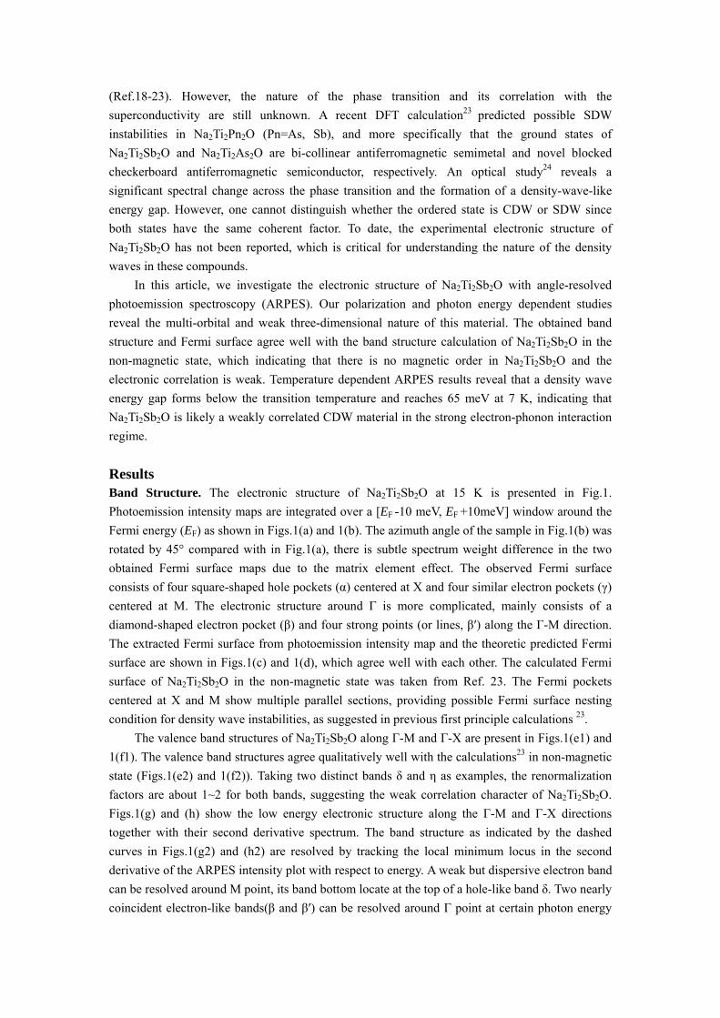
Results Band Structure. The electronic structure of Na2Ti2Sb2O at 15 K is presented in Fig.1.
Photoemission intensity maps are integrated over a [EF -10 meV, EF +10meV] window around the
Fermi energy (EF) as shown in Figs.1(a) and 1(b). The azimuth angle of the sample in Fig.1(b) was
rotated by 45° compared with in Fig.1(a), there is subtle spectrum weight difference in the two
obtained Fermi surface maps due to the matrix element effect. The observed Fermi surface
consists of four square-shaped hole pockets (α) centered at X and four similar electron pockets (γ)
centered at M. The electronic structure around Γ is more complicated, mainly consists of a
diamond-shaped electron pocket (β) and four strong points (or lines, β′) along the Γ-M direction.
The extracted Fermi surface from photoemission intensity map and the theoretic predicted Fermi
surface are shown in Figs.1(c) and 1(d), which agree well with each other. The calculated Fermi
surface of Na2Ti2Sb2O in the non-magnetic state was taken from Ref. 23. The Fermi pockets
centered at X and M show multiple parallel sections, providing possible Fermi surface nesting
condition for density wave instabilities, as suggested in previous first principle calculations 23.
The valence band structures of Na2Ti2Sb2O along Γ-M and Γ-X are present in Figs.1(e1) and
1(f1). The valence band structures agree qualitatively well with the calculations23 in non-magnetic
state (Figs.1(e2) and 1(f2)). Taking two distinct bands δ and η as examples, the renormalization
factors are about 1~2 for both bands, suggesting the weak correlation character of Na2Ti2Sb2O.
Figs.1(g) and (h) show the low energy electronic structure along the Γ-M and Γ-X directions
together with their second derivative spectrum. The band structure as indicated by the dashed
curves in Figs.1(g2) and (h2) are resolved by tracking the local minimum locus in the second
derivative of the ARPES intensity plot with respect to energy. A weak but dispersive electron band
can be resolved around M point, its band bottom locate at the top of a hole-like band δ. Two nearly
coincident electron-like bands(β and β′) can be resolved around Γ point at certain photon energy
along the Γ-M direction, while there is only one electron-like band β across EF near Γ along the
Γ-X direction. A hole-like band α crosses EF and forms the square-shaped pockets around X. The
overall measured electronic structure of Na2Ti2Sb2O agrees well with the calculations, and the
near-unity renormalization factor suggests that the ground state of Na2Ti2Sb2O is nonmagnetic and
the correlation is weak.
Fig.1 The electronic structure of Na2Ti2Sb2O at 15 K. (a) and (b), Photoemission intensity map at
EF integrated over [EF -10 meV, EF +10 meV], data were measured with 100 eV photons energy.
(c), The Fermi surface topology extract from (a) and (b). (d), The theoretic predicted Fermi
surface of Na2Ti2Sb2O. (e1-e2), The experiment and theoretic23 valence band structure along Γ-M
direction. (f1-f2), The experiment and theoretic23 valence band structure along Γ-X direction. Data
were measured with 100 eV photons energy in (e) and (f). (g1-g2), The photoemission intensity
and its second derivative of the intensity plot with respect to energy along Γ-M direction. (h1-h2),
The photoemission intensity and its second derivative of the intensity plot with respect to energy
along Γ-X direction, data were measured with 114 eV photons energy.
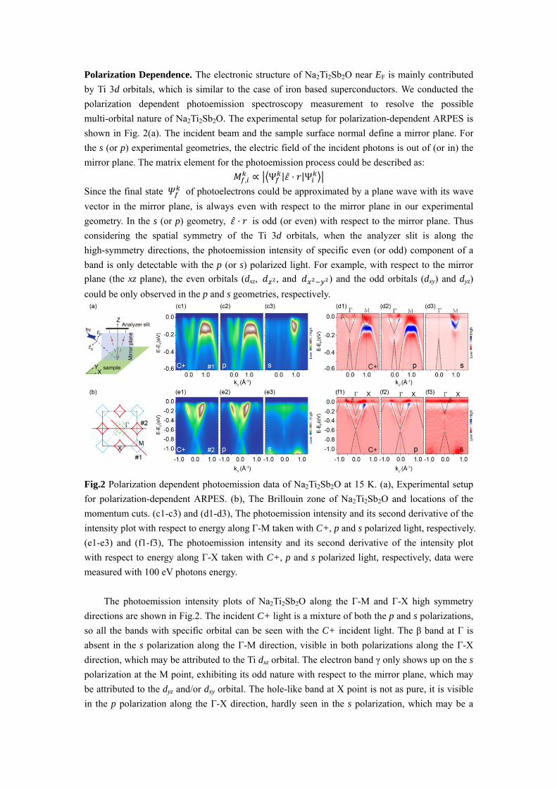
Polarization Dependence. The electronic structure of Na2Ti2Sb2O near EF is mainly contributed
by Ti 3d orbitals, which is similar to the case of iron based superconductors. We conducted the
polarization dependent photoemission spectroscopy measurement to resolve the possible
multi-orbital nature of Na2Ti2Sb2O. The experimental setup for polarization-dependent ARPES is
shown in Fig. 2(a). The incident beam and the sample surface normal define a mirror plane. For
the s (or p) experimental geometries, the electric field of the incident photons is out of (or in) the
mirror plane. The matrix element for the photoemission process could be described as:
, ∝ Ψ | ̂ |Ψ
Since the final state of photoelectrons could be approximated by a plane wave with its wave
vector in the mirror plane, is always even with respect to the mirror plane in our experimental
geometry. In the s (or p) geometry, ̂ is odd (or even) with respect to the mirror plane. Thus
considering the spatial symmetry of the Ti 3d orbitals, when the analyzer slit is along the
high-symmetry directions, the photoemission intensity of specific even (or odd) component of a
band is only detectable with the p (or s) polarized light. For example, with respect to the mirror
plane (the xz plane), the even orbitals (dxz, , and ) and the odd orbitals (dxy) and dyz)
could be only observed in the p and s geometries, respectively.
Fig.2 Polarization dependent photoemission data of Na2Ti2Sb2O at 15 K. (a), Experimental setup
for polarization-dependent ARPES. (b), The Brillouin zone of Na2Ti2Sb2O and locations of the
momentum cuts. (c1-c3) and (d1-d3), The photoemission intensity and its second derivative of the
intensity plot with respect to energy along Γ-M taken with C+, p and s polarized light, respectively.
(e1-e3) and (f1-f3), The photoemission intensity and its second derivative of the intensity plot
with respect to energy along Γ-X taken with C+, p and s polarized light, respectively, data were
measured with 100 eV photons energy.
The photoemission intensity plots of Na2Ti2Sb2O along the Γ-M and Γ-X high symmetry
directions are shown in Fig.2. The incident C+ light is a mixture of both the p and s polarizations,
so all the bands with specific orbital can be seen with the C+ incident light. The β band at Γ is
absent in the s polarization along the Γ-M direction, visible in both polarizations along the Γ-X
direction, which may be attributed to the Ti dxz orbital. The electron band γ only shows up on the s
polarization at the M point, exhibiting its odd nature with respect to the mirror plane, which may
be attributed to the dyz and/or dxy orbital. The hole-like band at X point is not as pure, it is visible
in the p polarization along the Γ-X direction, hardly seen in the s polarization, which may be a
mixture of different Ti 3d orbitals. In general, Na2Ti2Sb2O exhibits obvious polarization
dependence, which resembles the multi-band and multi-orbital nature of band structure of iron
pnictide superconductors25.
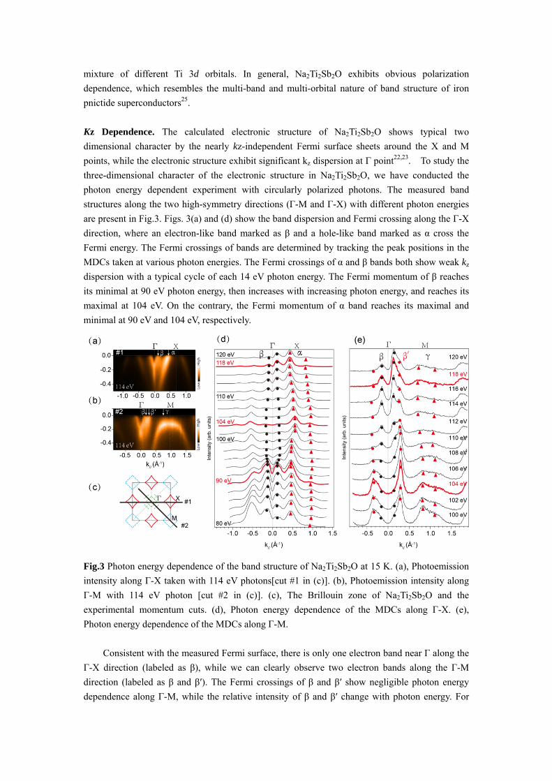
Kz Dependence. The calculated electronic structure of Na2Ti2Sb2O shows typical two
dimensional character by the nearly kz-independent Fermi surface sheets around the X and M
points, while the electronic structure exhibit significant kz dispersion at Γ point22,23. To study the
three-dimensional character of the electronic structure in Na2Ti2Sb2O, we have conducted the
photon energy dependent experiment with circularly polarized photons. The measured band
structures along the two high-symmetry directions (Γ-M and Γ-X) with different photon energies
are present in Fig.3. Figs. 3(a) and (d) show the band dispersion and Fermi crossing along the Γ-X
direction, where an electron-like band marked as β and a hole-like band marked as α cross the
Fermi energy. The Fermi crossings of bands are determined by tracking the peak positions in the
MDCs taken at various photon energies. The Fermi crossings of α and β bands both show weak kz
dispersion with a typical cycle of each 14 eV photon energy. The Fermi momentum of β reaches
its minimal at 90 eV photon energy, then increases with increasing photon energy, and reaches its
maximal at 104 eV. On the contrary, the Fermi momentum of α band reaches its maximal and
minimal at 90 eV and 104 eV, respectively.
Fig.3 Photon energy dependence of the band structure of Na2Ti2Sb2O at 15 K. (a), Photoemission
intensity along Γ-X taken with 114 eV photons[cut #1 in (c)]. (b), Photoemission intensity along
Γ-M with 114 eV photon [cut #2 in (c)]. (c), The Brillouin zone of Na2Ti2Sb2O and the
experimental momentum cuts. (d), Photon energy dependence of the MDCs along Γ-X. (e),
Photon energy dependence of the MDCs along Γ-M.
Consistent with the measured Fermi surface, there is only one electron band near Γ along the
Γ-X direction (labeled as β), while we can clearly observe two electron bands along the Γ-M
direction (labeled as β and β′). The Fermi crossings of β and β′ show negligible photon energy
dependence along Γ-M, while the relative intensity of β and β′ change with photon energy. For
instance at 104 eV, the β′ intensity is high, while the β intensity is low. With increasing photon
energy, the intensity of β′ decreases while that of β increases, reaching their minimum and
maximum at 118 eV, respectively. The relative intensity instead of Fermi crossing shows distinct
photon energy dependence for β and β′. For the γ band near the M point, its Fermi momentum
shows weak kz dispersion, with the minimal and maximum at 104 eV and 118 eV, respectively.
The theoretic predicted Fermi surface of Na2Ti2Sb2O shows cylinder Fermi sheets near M
and X and strong kz dependent Fermi sheet near Γ22,23, our photoemission data confirmed the two
dimensional character of the electronic structure at X and M. The weak photon energy dependence
of the electronic structure at Γ is not consistent with the theoretic calculation, and this discrepancy
may be due to the poor kz resolution of our ARPES experiment in the vacuum ultra-violet photon
energy range. It is known that the poor kz resolution would largely smear out the dispersive
information along kz for a fast-dispersive band, as likely observed here.
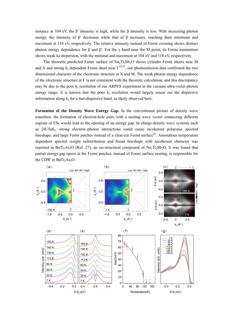
Formation of the Density Wave Energy Gap. In the conventional picture of density wave
transition, the formation of electron-hole pairs with a nesting wave vector connecting different
regions of FSs would lead to the opening of an energy gap. In charge-density wave systems such
as 2H-TaS2, strong electron–photon interactions could cause incoherent polaronic spectral
lineshape, and large Fermi patches instead of a clear-cut Fermi surface26. Anomalous temperature
dependent spectral weight redistribution and broad lineshape with incoherent character was
reported in BaTi2As2O (Ref. 27), an iso-structural compound of Na2Ti2Sb2O. It was found that
partial energy gap opens at the Fermi patches, instead of Fermi surface nesting, is responsible for
the CDW in BaTi2As2O.
Fig.4 The temperature dependence of Na2Ti2Sb2O band structure. (a) and (b), the photoemission
intensity map at 150 K and 7 K respectively, The intensity was integrated over a window (EF-10
meV, EF+10 meV). (c), The symmetrized photoemission intensity along Γ-X direction at 150 K
and 7 K, respectively. (d) and (e), Temperature dependence of the EDCs and symmetrized EDCs
at the Fermi crossing of M, the EDCs are integrated over the red rectangle area in (c). (f), The
temperature dependence of the CDW gap. The solid line is the fit to a mean field formula:
∆ 1 / , where Δ0=65 meV, TCDW=115 K. (g), Temperature dependence of the EDCs
around the Fermi crossing near Γ, the EDCs are integrated over the yellow rectangle area in (c).
Data were measured with 21.2 eV photons from a Helium discharge lamp.
The detailed temperature dependence of the low energy electronic structure of Na2Ti2Sb2O is
presented in Fig.4. The Fermi surface topologies of Na2Ti2Sb2O at 150 K and 7 K are rather
similar, but a dramatic spectra weight change can be observed around the X point. At 150 K,
which is above the phase transition temperature at 115 K, the spectra weight around X is quite
strong compared with those around the Γ point. At 7 K, which is well below the transition, the
spectral weight near X is obviously suppressed, while it was slightly enhanced near Γ. Fig.4(c)
shows the symmetrized spectrum along Γ-X. The band dispersion shows much alike at both
temperatures, but an energy gap opens at X point when it comes into the CDW/SDW state at 7 K.
We tracked the EDCs at the Fermi crossing of α band to reveal the CDW/SDW gap opening
behavior more precisely. The density of states near EF is obviously suppressed with decreasing
temperature; an energy gap opens at 113 K below the phase transition temperature of 115 K for
Na2Ti2Sb2O. The gap size increased with decreasing temperature, following the typical BCS
formula[Fig.4(f)]. The gap size get saturated at low temperature and the largest gap size is about
65 meV at 7 K, which give a large ratio of 2Δ/kBTs~13. The optical study24 revealed 2Δ/kBTs ~14,
in consistent with our findings. Such a large ratio indicates that this density wave system is in the
strong electron–photon coupling regime27.
Intriguingly, the photoemission spectrum of the electron band β around Γ shows a broad line
shape without a sharp quasiparticle peak near EF, and the spectral weight increases slightly with
deceasing temperature [Fig.4(g)]. Furthermore, the peak position moves slightly upward to EF
with deceasing temperature. Compared with the obvious gap opening behavior at X, it is safe to
conclude that the gap does not open near Γ. In consideration of the theoretic prediction that X and
M show multiple parallel sections, it is nature to deduce that Fermi surface nesting may happen
between the parallels sections of X and M. Due to the Matrix element effects, the spectral weight
near M is extremely weak for data taken with 21.2 eV photons, we thus cannot access the
temperature dependence there. On the other hand, the large energy scale spectral weight transfer
and broad lineshape, together with the large gap all suggest that the system is likely in the
strong-coupling regime, therefore as previously observed in BaTi2As2O(Ref. 27), 2H-TaS2(Ref. 26)
and 2H-NbSe2(Ref. 28), the low energy states over the entire Brillouin zone instead of only Fermi
surface might be responsible for the density wave formation.
Discussion It is crucial to understand the nature of the phase transition in the parent compounds of the newly
discovered titanium-based oxypnictide superconductors, which is an essential step towards a
thorough understanding of their superconducting mechanism. The SDW origin of the instability
would favor an unconventional superconductivity with a possibly sign-changing s-wave pairing,
while the CDW origin would suggest more conventional superconductivity with a simple s-wave
pairing. Previous experimental and theoretical studies have evoked much controversy on the
nature of the possible density wave transition. Our photoemission results are consistent with the
density wave origin of the phase transition in Na2Ti2Sb2O. Moreover, considering the qualitative
agreement of the experimental results and the calculated electronic structure23 in the nonmagnetic
states, and it is reasonable to deduce that it is possibly a conventional CDW transition in
Na2Ti2Sb2O. Although further low temperature ARPES or STM experiment is certainly needed to
reveal the exact nature of the superconducting samples, one can speculate that the
superconductivity in NaxBa1-xTi2Sb2O(Ref. 13) is likely due to electron phonon interactions, just
like in NbSe2(Ref. 28).
In summary, our experimental band structure agrees qualitatively well with the calculation23
in the nonmagnetic state, excluding the existence of possible magnetic order in Na2Ti2Sb2O.
Na2Ti2Sb2O shows obvious multi-band and multi orbital nature, which resemble the iron-based
superconductors. The electron band at M and the hole band at X show weak kz dispersion,
consistent with its layered crystal structure. We observe a large density wave gap of 65 meV which
forms near the X point at 7 K, indicating that Na2Ti2Sb2O is likely a CDW material. The weak
renormalization of the overall band structure indicates weak electron-electron correlation, while
the broad lineshape and large energy gap and spectral weight transfer suggest the system is likely
in the strong electron-phonon interaction regime.
Methods Sample synthesis. Single crystals of Na2Ti2Sb2O were synthesized by the self-flux method. A
mixture of Na, Sb, Ti and Ti2O3 with molar ratio of 18:18:1:4 is prepared and put into an
aluminum oxide crucible sealed inside a Ta tube. The mixture is gradually heated to 800 °C and
quenched to room temperature. Afterwards the mixture is heated at 1100 °C for 2 hours and cooled
to 500 °C at 5 °C/hour before quenched to room temperature.
ARPES measurement. The polarization and photon energy dependent ARPES data were taken at
the surface and interface spectroscopy beamline of the Swiss Light Source (SLS), The temperature
dependent ARPES data were taken with an in-house setup at Fudan University. All data were
collected with Scienta R4000 electron analyzers. The overall energy resolution was 15 meV or
better, and the typical angular resolution was 0.3◦. The samples were cleaved in-situ and measured
under ultrahigh vacuum better than 3×10⁻¹¹ mbar.
1. Bednorz, J. G. and K. A. Müller. Possible high Tc superconductivity in the Ba-La-Cu-O system. Z. Phys. B.
64, 189-193 (1986).
2. Kamihara, Y., et al. Iron-Based Layered Superconductor La(O1-xFx) FeAs (x=0.05−0.12) with Tc = 26 K. J.
Am. Chem. Soc. 130, 3296-3297 (2008).
3. Adam, A., and Schuster, H.-U. Darstellung und Kristallstruktur der Pnictidoxide Na2Ti2As2O und Na2Ti2Sb2O.
Z. Anorg. Allg. Chem. 584, 150-158 (1990).
4. Axtell, E. A., et al. Phase Transition and Spin-gap Behavior in a Layered Tetragonal Pnictide Oxide. J. Solid
State Chem.134, 423-426 (1997).
5. Ozawa, T. C., et al. Powder Neutron Diffraction Studies of Na2Ti2Sb2O and Its Structure–Property
Relationships. J. Solid State Chem. 153, 275-281(2000).
6. Ozawa, T., et al. Possible Charge-Density-Wave/Spin-Density-Wave in the Layered Pnictide−Oxides:
Na2Ti2Pn2O (Pn = As, Sb). Chem. Mat. 13, 1804-1810(2001).
7. Ozawa, T. C. and S. M. Kauzlarich. Single crystal growth and characterization of a layered transition metal
pnictide oxide: Na2Ti2Sb2O. J. Cryst. Growth. 265, 571-576 (2004).
8. Ozawa, T. C. and S. M. Kauzlarich. Chemistry of layeredd-metal pnictide oxides and their potential as
candidates for new superconductors. Sci. Technol. Adv. Mater. 9, 033003 (2008).
9. Liu, R. H., et al. Physical properties of the layered pnictide oxides Na2Ti2P2O (P=As, Sb). Phys. Rev. B
80,144516(2009).
10. Wang, X. F., et al. Structure and physical properties for a new layered pnictide-oxide: BaTi2As2O. J. Phys.
Condens .Matter. 22, 075702 (2010).
11. Liu, R. H., et al. Structure and Physical Properties of the Layered Pnictide-Oxides:(SrF)2Ti2Pn2O (Pn = As, Sb)
and (SmO)2Ti2Sb2O. Chem. Mat. 22, 1503-1508 (2010).
12. Yajima, T., et al. Superconductivity in BaTi2Sb2O with a d1 Square Lattice. J. Phys. Soc. Jpn. 81,
103706(2012).
13. Doan, P., et al. Ba1-xNaxTi2Sb2O (0.0≤x≤0.33): A Layered Titanium-Based Pnictide Oxide Superconductor. J.
Am. Chem. Soc. 134, 16520-16523(2012).
14. Gooch, M., et al. Weak coupling BCS-like superconductivity in the pnictide oxide Ba1−xNaxTi2Sb2O (x=0 and
0.15). Phys. Rev. B 88, 064510 (2013).
15. Litvinchuk, A. P., et al. Lattice dynamics of Ti-based pnictide superconductors Ba1−xNaxTi2Sb2O. Phys. Rev. B
87, 064505(2013).
16. Von Rohr, F., et al. Conventional superconductivity and charge-density-wave ordering in Ba1−xNaxTi2Sb2O.
Phys. Rev. B 88, 140501 (2013)
17. Zhai, H.-F., et al. Superconductivity, charge- or spin-density wave, and metal-nonmetal transition in
BaTi2(Sb1−xBix)2O. Phys. Rev. B. 87, 100502 (2013).
18. Biani, F. F. d., et al. Concerning the Resistivity Anomaly in the Layered Pnictide Oxide Na2Ti2Sb2O. Inorg.
Chem. 37, 5807–5810(1998).
19. Pickett, W. E. Electronic instability in inverse-K2NiF4-structure Na2Ti2Sb2O. Phys. Rev. B 58, 4335-4340
(1998).
20. Singh, D. J. Electronic structure, disconnected Fermi surfaces and antiferromagnetism in the layered pnictide
superconductor NaxBa1−xTi2Sb2O. New J. Phys. 14, 123003(2012).
21. Subedi, A. Electron-phonon superconductivity and charge density wave instability in the layered
titanium-based pnictide BaTi2Sb2O. Phys. Rev. B 87, 054506 (2013).
22. Suetin, D. V. and A. L. Ivanovskii. Structural, electronic properties, and chemical bonding in quaternary
layered titanium pnictide-oxides Na2Ti2Pn2O and BaTi2Pn2O (Pn=As, Sb) from FLAPW–GGA calculations. J.
Alloy. Compd. 564,117-124(2013).
23. Yan, X.-W. and Z.-Y. Lu. Layered pnictide-oxide Na2Ti2Pn2O (Pn=As, Sb): a candidate for spin density waves.
J. Phys-Condens. Mat. 25, 365501(2013).
24. Huang, Y., et al. Formation of the density wave energy gap in Na2Ti2Sb2O: An optical spectroscopy study.
Phys. Rev. B 87, 100507(2013).
25. Zhang, Y., et al. Orbital characters of bands in the iron-based superconductor BaFe1.85Co0.15As2. Phys. Rev. B
83, 054510 (2011).
26. Shen, D. W., et al. Novel Mechanism of a Charge Density Wave in a Transition Metal Dichalcogenide. Phys.
Rev. Lett. 99, 216404(2007).
27. Xu, H. C., et al. Electronic structure of the BaTi2As2O parent compound of the titanium-based oxypnictide
superconductor. Phys. Rev. B 89, 155108 (2014).
28. Shen, D. W., et al. Primary Role of the Barely Occupied States in the Charge Density Wave Formation of
NbSe2. Phys. Rev. Lett. 101, 226406 (2008).
Acknowledgements We thank Dr. M. Shi for the experimental support at Swiss Light Source(SLS). We gratefully
acknowledge helpful discussions with Prof. N. L. Wang. This work is supported in part by the
National Science Foundation of China and the National Basic Research Program of China (973
Program) under Grants No. 2012CB921400, No. 2011CB921802, No.2011CBA00112, No.
2011CB309703, and No. 91026016. The single crystal growth work at the University of Tennessee
was supported by the U.S. DOE, BES, through Contract No. DE-FG02-05ER46202.
Author contributions S. Y. Tan, J. Jiang, Z. R. Ye, X. H. Niu and B. P. Xie performed the ARPES measurements. Y.
Song, C. L. Zhang and P. C. Dai provided the single crystal samples. S. Y. Tan and D. L. Feng
analyzed the ARPES data, S. Y. Tan and D. L. Feng wrote the paper. D. L. Feng and X. C. Lai are
responsible for the infrastrure, projection and planning.
Additional information Competing financial interests: The authors declare no competing financial interests.
Correspondence and requests for materials should be addressed to D.L.Feng


![An investigation of surface electronic structure and …...DanishPhysical Society Annual Meeting, Nyborg, Denmark, June 2001. ‘Photoemission lineshapeat finite temperature’ [FF10]](https://img.pdfslide.net/doc/110x75/5f789393ff76b14e8f6f0122/an-investigation-of-surface-electronic-structure-and-danishphysical-society.jpg)