Embed Size (px)
Citation preview
VTT PU
BLIC
ATIO
NS 692
Photonic module integration based on silicon, ceram
ic and plastic...Keränen
Kimm
o
ESPOO 2008ESPOO 2008ESPOO 2008ESPOO 2008ESPOO 2008 VTT PUBLICATIONS 692
Kimmo Keränen
Photonic module integrationbased on silicon, ceramic andplastic technologies
In this work, we have developed and evaluated silicon, multilayer ceramicand plastic technologies in implementation of photonic modules utilizingpassive alignment between critical devices and components. Silicontechnology can provide sub-micron alignment accuracy between devicesdue to the lithographic manufacturing process. Silicon technology,however, is not yet capable of producing effective light sources throughmonolithic integration and hybrid integration has to still be applied inphotonic module integration. Multilayer ceramic technology substrate isdeveloped to provide 3 … 10 µm transverse alignment tolerance betweenlaser diode and fiber in passive alignment. The achieved tolerance isadequate for multimode applications, but inadequate for single modeapplications. Utilization of lithographic tooling process and light sensitivecoating materials with multilayer ceramic substrates seems to be the bestapproach to achieve single mode tolerances in the future. In-moldintegration technology utilizing bare devices assembled on substrates andusing these sub-modules as inserts in injection molding process isevaluated by implementing and testing HVCSEL illuminator andmicroscope lens for mobile phone demonstrators. Passive alignmentinaccuracy below +/- 60 µm is achieved, which is adequate for thepresented applications and also for many other illumination and sensingapplications.
123456789012345678901234567890121234567890123456789012345678901212345678901234567812345678901234567890123456789012123456789012345678901234567890121234567890123456781234567890123456789012345678901212345678901234567890123456789012123456789012345678123456789012345678901234567890121234567890123456789012345678901212345678901234567812345678901234567890123456789012123456789012345678901234567890121234567890123456781234567890123456789012345678901212345678901234567890123456789012123456789012345678123456789012345678901234567890121234567890123456789012345678901212345678901234567812345678901234567890123456789012123456789012345678901234567890121234567890123456781234567890123456789012345678901212345678901234567890123456789012123456789012345678123456789012345678901234567890121234567890123456789012345678901212345678901234567812345678901234567890123456789012123456789012345678901234567890121234567890123456781234567890123456789012345678901212345678901234567890123456789012123456789012345678123456789012345678901234567890121234567890123456789012345678901212345678901234567812345678901234567890123456789012123456789012345678901234567890121234567890123456781234567890123456789012345678901212345678901234567890123456789012123456789012345678123456789012345678901234567890121234567890123456789012345678901212345678901234567812345678901234567890123456789012123456789012345678901234567890121234567890123456781234567890123456789012345678901212345678901234567890123456789012123456789012345678123456789012345678901234567890121234567890123456789012345678901212345678901234567812345678901234567890123456789012123456789012345678901234567890121234567890123456781234567890123456789012345678901212345678901234567890123456789012123456789012345678123456789012345678901234567890121234567890123456789012345678901212345678901234567812345678901234567890123456789012123456789012345678901234567890121234567890123456781234567890123456789012345678901212345678901234567890123456789012123456789012345678123456789012345678901234567890121234567890123456789012345678901212345678901234567812345678901234567890123456789012123456789012345678901234567890121234567890123456781234567890123456789012345678901212345678901234567890123456789012123456789012345678123456789012345678901234567890121234567890123456789012345678901212345678901234567812345678901234567890123456789012123456789012345678901234567890121234567890123456781234567890123456789012345678901212345678901234567890123456789012123456789012345678123456789012345678901234567890121234567890123456789012345678901212345678901234567812345678901234567890123456789012123456789012345678901234567890121234567890123456781234567890123456789012345678901212345678901234567890123456789012123456789012345678123456789012345678901234567890121234567890123456789012345678901212345678901234567812345678901234567890123456789012123456789012345678901234567890121234567890123456781234567890123456789012345678901212345678901234567890123456789012123456789012345678123456789012345678901234567890121234567890123456789012345678901212345678901234567812345678901234567890123456789012123456789012345678901234567890121234567890123456781234567890123456789012345678901212345678901234567890123456789012123456789012345678123456789012345678901234567890121234567890123456789012345678901212345678901234567812345678901234567890123456789012123456789012345678901234567890121234567890123456781234567890123456789012345678901212345678901234567890123456789012123456789012345678123456789012345678901234567890121234567890123456789012345678901212345678901234567812345678901234567890123456789012123456789012345678901234567890121234567890123456781234567890123456789012345678901212345678901234567890123456789012123456789012345678123456789012345678901234567890121234567890123456789012345678901212345678901234567812345678901234567890123456789012123456789012345678901234567890121234567890123456781234567890123456789012345678901212345678901234567890123456789012123456789012345678123456789012345678901234567890121234567890123456789012345678901212345678901234567812345678901234567890123456789012123456789012345678901234567890121234567890123456781234567890123456789012345678901212345678901234567890123456789012123456789012345678123456789012345678901234567890121234567890123456789012345678901212345678901234567812345678901234567890123456789012123456789012345678901234567890121234567890123456781234567890123456789012345678901212345678901234567890123456789012123456789012345678123456789012345678901234567890121234567890123456789012345678901212345678901234567812345678901234567890123456789012123456789012345678901234567890121234567890123456781234567890123456789012345678901212345678901234567890123456789012123456789012345678123456789012345678901234567890121234567890123456789012345678901212345678901234567812345678901234567890123456789012123456789012345678901234567890121234567890123456781234567890123456789012345678901212345678901234567890123456789012123456789012345678123456789012345678901234567890121234567890123456789012345678901212345678901234567812345678901234567890123456789012123456789012345678901234567890121234567890123456781234567890123456789012345678901212345678901234567890123456789012123456789012345678123456789012345678901234567890121234567890123456789012345678901212345678901234567812345678901234567890123456789012123456789012345678901234567890121234567890123456781234567890123456789012345678901212345678901234567890123456789012123456789012345678123456789012345678901234567890121234567890123456789012345678901212345678901234567812345678901234567890123456789012123456789012345678901234567890121234567890123456781234567890123456789012345678901212345678901234567890123456789012123456789012345678
ISBN 978-951-38-7115-4 (soft back ed.) ISBN 978-951-38-7116-1 (URL: http://www.vtt.fi/publications/index.jsp)ISSN 1235-0621 (soft back ed.) ISSN 1455-0849 (URL: http://www.vtt.fi/publications/index.jsp)
Julkaisu on saatavana Publikationen distribueras av This publication is available from
VTT VTT VTTPL 1000 PB 1000 P.O. Box 1000
02044 VTT 02044 VTT FI-02044 VTT, FinlandPuh. 020 722 4520 Tel. 020 722 4520 Phone internat. + 358 20 722 4520
http://www.vtt.fi http://www.vtt.fi http://www.vtt.fi

VTT PUBLICATIONS 692
Photonic module integration based on silicon, ceramic and plastic
technologies
Kimmo Keränen
Academic dissertation for the degree of Doctor of Technology to be presented, with the permission of the Department of Electrical Engineering of the University
of Oulu, for public discussion in the Auditorium L6, Linnanmaa, on November 14th, at 12 oclock noon.
ISBN 978-951-38-7115-4 (soft back ed.) ISSN 1235-0621 (soft back ed.)
ISBN 978-951-38-7116-1 (URL: http://www.vtt.fi/publications/index.jsp) ISSN 1455-0849 (URL: http://www.vtt.fi/publications/index.jsp)
Copyright © VTT Technical Research Centre of Finland 2008
JULKAISIJA UTGIVARE PUBLISHER
VTT, Vuorimiehentie 3, PL 1000, 02044 VTT puh. vaihde 020 722 111, faksi 020 722 4374
VTT, Bergsmansvägen 3, PB 1000, 02044 VTT tel. växel 020 722 111, fax 020 722 4374
VTT Technical Research Centre of Finland, Vuorimiehentie 3, P.O.Box 1000, FI-02044 VTT, Finland phone internat. +358 20 722 111, fax + 358 20 722 4374
VTT, Kaitoväylä 1, PL 1100, 90571 OULU puh. vaihde 020 722 111, faksi 020 722 2320
VTT, Kaitoväylä 1, PB 1100, 90571 ULEÅBORG tel. växel 020 722 111, fax 020 722 2320
VTT Technical Research Centre of Finland, Kaitoväylä 1, P.O. Box 1100, FI-90571 OULU, Finland phone internat. +358 20 722 111, fax +358 20 722 2320
Technical editing Maini Manninen Edita Prima Oy, Helsinki 2008
3
Keränen, Kimmo. Photonic module integration based on silicon, ceramic and plastic technologiesEspoo 2008. VTT Publications 692. 100 p. + app. 72 p.
Keywords device, multi-layer ceramic, plastic, substrate, module, alignment structures,passive alignment, hermetic, encapsulation, integration, injection molding, cost-efficiency
Abstract This thesis reports the main results in photonic module integration using silicon, multilayer ceramic and plastic technologies.
In order to implement high-performance photonic modules the accurate alignment between critical devices and components is very essential. Cost-efficient photonic modules in volume production can be achieved, when the alignment of devices and components is implemented passively. Utilization of lithographic manufacturing process in silicon processing ensures that the required alignment tolerances between devices are well possible to achieve with photonic modules. The capability of silicon technology to produce a monolithically integrated photonic sensor system, a miniaturized infrared (IR) spectrometer, is studied and evaluated in this work.
The capability of a multilayer ceramics substrate to act as an optical platform for a miniature profilometer and an optical bench for passive alignment of laser chip and fiber is evaluated. The components of the miniature profilometer are aligned below +/- 100 µm transverse tolerance passively, which enables operational sensor module implementation. The multilayer ceramic optical bench substrate demonstrates transverse passive alignment tolerances of 3 10 µm in laser-to-fiber coupling. The tolerances are at adequate level for multimode couplings, but inadequate for single-mode couplings.
Transverse alignment tolerances below +/-60 µm are achieved between source and lens surface using in-mold integration with a novel VCSEL illuminator. In addition, a fully operational microscope lens system for Nokia 6630 mobile phone using in-mold integration is designed, implemented and evaluated.
4
Preface The work covered by this thesis has been carried out at VTT Technical Research Centre of Finland (VTT) during the years 19972007. The major part of the research was executed in the projects NIRSARI, MODIR, SIMO and AKTIVA, funded mainly by Finnish Funding Agency for Technology and Innovation (Tekes) and VTT.
I wish to thank my supervisors, Prof. Pentti Karioja (VTT) and Prof. Risto Myllylä (University of Oulu), for their guidance, support and encouragement during the course of this research. I thank Prof. Harri Kopola (VTT) for encouragement to complete post-graduate studies and his effort to generate research projects. Dr. Ari Tervonen (Helsinki University of Technology) and Dr. Klaus-Dieter Lang (Fraunhofer Institut) are greatly acknowledged for comprehensive peer-reviewing of the manuscript of the thesis. Great thanks to Janne Aikio, Veli Heikkinen and Jukka-Tapani Mäkinen for their expert assistance and support. I thank all my co-workers for their great attitude and the assistance they have given. I especially want to thank Mikko Heikkinen, Jussi Hiltunen, Marianne Hiltunen, Jouni Kangas, Risto Karjalainen, Sami Karjalainen, Mikko Karppinen, Kari Kautio, Sari Kivelä, Pentti Korhonen, Jyrki Ollila, Jarno Petäjä, Kari Rönkä, Jussi Tenhunen and Airi Weissenfelt. Furthermore, I thank Seija Rajaniemi for helping me to obtain the scientific literature and Tuija Soininen for helping me to improve the visualization of the publications.
The financial stimulation funds received from the Nokia Research Foundation and the Ulla Tuominen Foundation are gratefully acknowledged. I would also like to acknowledge the financial support for the finalization of the thesis from the Infotech Oulu.
My sons Eemeli, Kasperi and Jussi have to be greatly acknowledged for giving me the opportunity to experience life with my body and soul in addition to the confined techno-scientific approach.
Finally, I thank Minna for the motivation and encouragement to complete this thesis. Oulu, September 2008 Kimmo Keränen
5
Contents
Abstract ................................................................................................................. 3
Preface .................................................................................................................. 4
List of publications ............................................................................................... 7
Authors contribution............................................................................................ 9
List of abbreviations and symbols ...................................................................... 10
1. Introduction................................................................................................... 17 1.1 Background and motivation ................................................................ 17 1.2 Scope and objectives of the thesis ....................................................... 21 1.3 Contribution of the thesis .................................................................... 22
2. Main integration types for photonic modules ............................................... 24 2.1 Monolithic integration ......................................................................... 24 2.2 Hybrid integration ............................................................................... 29
3. Manufacturing technologies for optics and opto-mechanics for photonic modules............................................................................................................... 35
3.1 Silicon surface micromachining .......................................................... 35 3.2 Traditional and modern lens tooling.................................................... 36 3.3 Molding technologies .......................................................................... 38
3.3.1 Molding technology variations ............................................... 38 3.3.2 Thermoplastic materials .......................................................... 40 3.3.3 Tool manufacturing technologies............................................ 42
3.4 Polymer encapsulation of electronics and integration with mechanics and optics using injection molding...................................................... 43
4. Photonic module integration demonstrators ................................................. 45 4.1 Miniature infrared spectrometer .......................................................... 45
4.1.1 Devices and operational principle of the spectrometer ........... 45 4.1.2 System optical modeling ......................................................... 47 4.1.3 Packaging of the spectrometer ................................................ 50 4.1.4 Characterization of the spectrometer module.......................... 52
6
4.1.5 Evaluation of the spectrometer implementation...................... 53 4.2 Optical profilometer implemented on an LTCC substrate .................. 54
4.2.1 Sensor module concept ........................................................... 54 4.2.2 Transmitter and receiver optics of the sensor.......................... 55 4.2.3 LTCC platform of the sensor .................................................. 55 4.2.4 Optomechanics of the sensor .................................................. 56 4.2.5 Performance of the profilometer ............................................. 56 4.2.6 Evaluation of the profilometer implementation ...................... 57
4.3 Passive alignment laser modules based on an LTCC substrate ........... 58 4.3.1 Passive alignment features on an LTCC substrate .................. 59 4.3.2 Optical modeling of the laser-to-fiber coupling...................... 60 4.3.3 Thermal management of high power laser diode .................... 63 4.3.4 Packaging of the modules ....................................................... 64 4.3.5 Characterizations of the modules ............................................ 66 4.3.6 Evaluation of the passive alignment laser modules based on
LTCC technology.................................................................... 70 4.4 In-mold integration of VCSEL collimator........................................... 71
4.4.1 Manufacturing concept............................................................ 71 4.4.2 Design of the demonstrator module ........................................ 71 4.4.3 Design and implementation of the sub-modules and tools...... 72 4.4.4 Processing of the collimator.................................................... 73 4.4.5 Testing of the collimator ......................................................... 74
4.5 In-mold integration of microscope lens for mobile phone .................. 77 4.5.1 Design of the microscope module........................................... 77 4.5.2 Design and implementation of the sub-modules and tools...... 80 4.5.3 Processing of the microscope lens .......................................... 81 4.5.4 Testing and characterization of the microscope lens............... 82 4.5.5 Evaluation of the in-mold integrated demonstrators ............... 85
5. Discussion..................................................................................................... 87
6. Summary....................................................................................................... 91
References........................................................................................................... 93 Appendices
Papers IVI
Appendices of this publication are not included in the PDF version.Please order the printed version to get the complete publication (http://www.vtt.fi/publications/index.jsp)
7
List of publications This thesis is based on the following original publications, which are referred to in the text by their Roman numerals:
I: Keränen, K., Karioja, P., Blomberg, M., Tenhunen, J., Rusanen, O. & Kopola, H. 2001. Miniaturization and module integration of an infrared spectrometer. Opt. Eng., Vol. 40, No. 10, pp. 23082314.
II: Heikkinen, V., Heikkinen, M., Keränen, K., Mitikka, R., Putila, V.-P. & Tukkiniemi, K. 2005. Laser profilometer module based on a low-temperature cofired ceramic substrate. Opt. Eng., Vol. 44, No. 9, pp. 093603-17.
III: Keränen, K., Mäkinen, J.-T., Kautio, K., Ollila, J., Petäjä, J., Heikkinen, V., Heilala, J. & Karioja, P. 2006. Fiber pigtailed multimode laser module based on passive device alignment on an LTCC substrate. IEEE Trans. Adv. Packag., Vol. 29, No. 3, pp. 463472.
IV: Keränen, K., Ollila, J., Mäkinen, J.-T., Korhonen, P. Kautio, K., Heikkinen, V. & Karioja, P. Hermetic fiber pigtailed laser module utilizing passive device alignment on an LTCC substrate. Accepted for publication in IEEE Trans. Adv. Packag.
V: Keränen, K., Saastamoinen, T., Mäkinen, J.-T., Silvennoinen, M., Mustonen, I., Vahimaa, P., Jääskeläinen, T., Lehto, A., Ojapalo, A., Schorpp, M., Hoskio, P. & Karioja, P. 2007. Injection moulding integration of a red VCSEL illuminator module for a hologram reader sensor. Proc. of SPIE, Vol. 6585, Pp. 658503-110.
VI: Mäkinen, J.-T., Keränen, K., Hakkarainen, J., Silvennoinen, M., Salmi, T., Syrjälä, S., Ojapalo, A., Schorpp, M., Hoskio, P. & Karioja, P. 2007. Inmould integration of a microscope add-on system to a 1.3 Mpix camera phone. Proc. of SPIE, Vol. 6585, Pp. 658507-110.
8
Publication I presents the design, simulation, implementation and characterization of the miniature IR spectrometer demonstrator based on a silicon surface micromechanics technology.
Publication II presents the design, simulation, implementation and characterization of the optical profilometer demonstrator implemented on an LTCC substrate.
Publication III presents the design, simulation, implementation and characterization of the passively aligned fiber pigtailed multimode laser module based on the development of an LTCC precision substrate.
Publication IV presents the design, simulation, implementation and characterization of the hermetic passively aligned laser module. The implementation of the passive alignment is based on the work in LTCC precision substrate development described in Publication III.
Publication V presents the design, implementation and characterization of the in-mold integrated VCSEL collimator module.
Publication VI presents the design, simulation, implementation and characterization of the in-mold integrated microscope add-on lens module for a mobile phone.
9
Authors contribution The results presented in this thesis have been achieved in co-operation within the research group and with the co-authors.
For publication I, the author was responsible for the module integration project. He participated in the packaging design and made the optical modeling and simulations, except for the Fabry-Perot analytical model, which was created by Mr. Jussi Tenhunen. The author characterized the modules and analyzed the results. The manuscript was prepared by him.
For publication II, the author generated the concept of the measurement system and performed the conceptual system design. He also designed module optics and actively participated in the preparation of the manuscript.
For publication III, the author was responsible for the module integration project. He participated in the characterization of the demonstrator modules and analysis of the results. The manuscript was prepared by him.
For publication IV, the author was responsible for the module integration project. He participated in the module characterizations. The manuscript was prepared by him.
For publication V, the author was responsible for the module integration project. He participated in the characterization of the demonstrator modules and analyzed the results. He performed the cost-of-ownership modeling. The manuscript was prepared by him.
For publication VI, the author was responsible for the module integration project. He participated in the characterization of the demonstrator modules and analysis of the results. He participated in the preparation of the manuscript.

10
List of abbreviations and symbols 2D two-dimensional
3D three-dimensional
ε emissivity of the radiator
λ wavelength
θ angle
σ Stefan-Bolzmann constant ≈ 5.67 × 10⁻⁸ W/m2K4
A surface area
APB aligned pillar bonding
AR anti-reflection
ASAP advanced system analysis program
BPSG borophosphorsilicate glass
c speed of light in vacuum
CAD computer-aided design
CCD charge-coupled device
CMOS complementary metal oxide semiconductor
CNC computer numerical control
COC cyclo-olefin copolymer

11
CTE coefficient of thermal expansion
CVD chemical vapor deposition
d distance
DGW dielectric growth window
DIL dual-in-line
DOE diffractive optics element
EB electron beam
EDM electric discharge machining
EEL edge emitting laser
EFL effective focal length
EoE epitaxy on electronics
FFT fast Fourier transform
FOV field-of-view
FPI Fabry-Perot interferometer
FR4 flame retardant class 4 fiberglass epoxy electronic substrate
FR5 flame retardant class 5 fiberglass epoxy electronic substrate

12
FTIR Fourier transform infrared
FWHM full width half maximum
GaAs gallium arsenide
GaInAlAs gallium indium aluminum arsenide
GaInAsP gallium indium arsenic phosphide
GaN gallium nitride
h Plancks constant ≈ 6.63 ×10⁻³⁴ Js
HF hydrofluoric
H-GaAs high-integration gallium arsenide
IC integrated circuit
InGaP indium gallium phosphide
InP indium phosphide
IR infrared
LBBλ spectral radiance of the blackbody
LCP liquid crystal polymer
LD laser diode
LED light emitting diode
LIGA lithographie galvanoformung abformung
LiNbO3 lithium niobate

13
LTCC low-temperature cofired ceramics
Mbb exitance of the emitter surface
MBE molecular beam epitaxy
MEMS micro-electro-mechanical system
MESFET metal semiconductor field effect transistor
MOCVD metal organic chemical vapor deposition
MOEMS micro-optical electro-mechanical system
MSM metal semiconductor metal
MTF modulation transfer function
n refractive index
NA numerical aperture
NIR near-infrared
OIC optical integrated circuit
OPFET optically enhanced field effect transistor
PA polyamide
PC polycarbonate
PECVD plasma-enhanced chemical vapor deposition
PEEK polyetheretherketone
PE-HD polyethylene high density

14
PE-LD polyethylene low density
PFA perfluoralkoxy
PIC photonic integrated circuit
PLC planar waveguide circuit
PMMA polymethyl methacrylate
POM polyoxymethylene
PS polystyrene
PSU polysulfone
PTFE polytetrafluoroethylene
R reflectivity
RIE reactive ion etching
RMS root mean square
RTD resonant tunneling diode
SEED self electro-optical device
Si silicon
SiO2-Si quartz-silicon
SMD surface mount device
SNR signal-to-noise ratio
SOB silicon-optical-bench

15
SOI silicon-on-insulator
SonG silicon-on-gallium arsenide
SOS silicon-on-sapphire
SPM scanning probe microscopy
SSC spot size converter
T temperature
TFPI transmission of the FPI
UV ultraviolet
VCSEL vertical cavity surface emitting laser
VGA video graphics array
VLSI very-large-scale integration

16
17
1. Introduction
1.1 Background and motivation
The performance of electronic circuits based on silicon integrated circuit (IC) technology doubled every twelve months in the 1960s and every twenty-four months in the 1970s (Moore, 1998). This exponential progress is frequently used as an example of the rapid and still ongoing evolution of microelectronics. Each reduction in the typical device feature size of most very-large-scale-integration (VLSI) circuits has meant that more gates could be fabricated in the unit area of a chip. The feature and device size reduction development is known as Moores law and it has implied an increase in the internal computational bandwidth of the chips. State-of-the-art Intel Xeon processor is implemented using 65-nm 8-metal silicon technology and it has a total of 1.3 billion transistors (Chang et al., 2008).
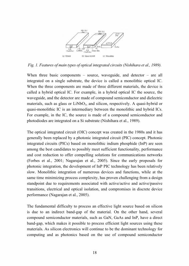
Connections between VLSI chips to one another with wire interconnects, however, is insufficient because the aggregate communication bandwidth of the wire links is only a small fraction of the internal bandwidth of the chips (Towe, 2000). The wire interconnections are not likely to meet the chip-to-chip and board-to-board communication needs of future high-performance systems. Use of optics at the chip-to-chip and board-to-board interconnections is being explored by a number of groups and it is seen as promising alternative for interconnections (Liu et al., 2000). An optical integrated circuit (OIC) is a thin-film-type optical circuit designed to have a certain function by integration of a laser diode, switches/modulators, waveguides and photo detectors, on a single substrate. OICs have been divided into three types from the standpoint of materials. Features of each type are shown in Fig. 1.
18
Fig. 1. Features of main types of optical integrated circuits (Nishihara et al., 1989).
When three basic components source, waveguide, and detector are all integrated on a single substrate, the device is called a monolithic optical IC. When the three components are made of three different materials, the device is called a hybrid optical IC. For example, in a hybrid optical IC the source, the waveguide, and the detector are made of compound semiconductor and dielectric materials, such as glass or LiNbO3, and silicon, respectively. A quasi-hybrid or quasi-monolithic IC is an intermediary between the monolithic and hybrid ICs. For example, in the IC, the source is made of a compound semiconductor and photodiodes are integrated on a Si substrate (Nishihara et al., 1989).
The optical integrated circuit (OIC) concept was created in the 1980s and it has generally been replaced by a photonic integrated circuit (PIC) concept. Photonic integrated circuits (PICs) based on monolithic indium phosphide (InP) are seen among the best candidates to possibly meet sufficient functionality, performance and cost reduction to offer compelling solutions for communications networks (Forbes et al., 2001; Nagarajan et al., 2005). Since the early proposals for photonic integration, the development of InP PIC technology has been relatively slow. Monolithic integration of numerous devices and functions, while at the same time minimizing process complexity, has proven challenging from a design standpoint due to requirements associated with active/active and active/passive transitions, electrical and optical isolation, and compromises in discrete device performance (Nagarajan et al., 2005).
The fundamental difficulty to process an effective light source based on silicon is due to an indirect band-gap of the material. On the other hand, several compound semiconductor materials, such as GaN, GaAs and InP, have a direct band-gap, which makes it possible to process efficient light sources using these materials. As silicon electronics will continue to be the dominant technology for computing and as photonics based on the use of compound semiconductor
19
technologies will dominate in communications, the effective integration of these two technologies in optical interconnection systems is extremely alluring. The effective integration of silicon VLSI electronics technology with compound semiconductor photonics technology, however, seems to be impractical due to the incompatibility of these two processing technologies. In addition, novel processing technologies based on the use of silicon are not capable in the near future, maybe never, to produce efficient and commercially feasible light sources (Ng et al., 2001; Castagna et al., 2003). Effective integration of silicon electronics technology with photonics technology for manufacturable, practical and cost-efficient chips seems to be impossible in the near future and hybrid integration technologies still seem to be needed.
The present silicon processing industry produces a diverse spectrum of integrated circuits in electronics including amplifiers, converters, multiplexers and processors. The traditional electronic package hierarchy for microelectronics products can be listed as follows (Tummala & Rymaszewski, 1989).
1. IC chips are packaged to a chip capsule, a module, in the first level of packaging.
2. Modules are assembled on multilayer cards in the second level of packaging.
3. Cards are assembled on boards in the third level of packaging.
4. Boards are assembled in gates and interconnected by pluggable cables in the fourth level of packaging.
Compound semiconductor processing industry produces effective solid state emitters, such as light emitting diodes (LEDs), laser diodes (LDs) and detectors utilized in various sensing and communication applications. In the packaging of hybrid integrated photonic modules, the bare semiconductor devices have to be refined to the component level by implementing essential internal and external electrical, optical, mechanical and thermal interfaces in a packaging process, as well as protection against environmental stresses, such as electro-magnetic interference, thermal variations, mechanical vibrations and shocks. The encapsulation of the bare devices also provides a shield against humidity, dust and corrosive chemicals in order to ensure reliable operation of devices. It is also
20
possible to pass component or sub-module packaging level and apply bare semiconductor devices in module implementations (Paper I, Paper III, Paper IV, Paper V, Paper VI).
The bonding and encapsulation of the source and detector devices is an essential part of photonic module integration, but the integration contains also implementation of functionalities needed in the application. Implementation of functionalities typically requires the adding of several different types of optical components, such as filters and lenses, to the system. Effective integration technologies to solve efficiently light coupling challenges from chip-to-chip and board-to-board are pursued for photonic communication solutions, especially in single-mode applications, where sub-micrometer alignment accuracy between devices is required. In several other applications light coupling challenges are diverse, but typically the required alignment accuracy between devices is not as high as in communication applications.
Optical interconnections is one very important application area for photonic modules, but the use and importance of photonics is steadily increasing in medical, lighting, automotive, security/biometrics, consumer electronics and sensors in general as well. Several hundreds millions mobile phones containing a camera module are sold annually and the annual growth rate is typically around ten percent. At the supermarkets most of the tills work in conjunction with optical bar code scanning systems. Music and movies are available on CD and/or DVD players and computers store data on optical disks. Information from the disks is read using laser diodes and sophisticated optics. Cars are generally equipped with brake and tail signals implemented with LED lamps. In addition, the car indoor lighting is increasingly implemented with LED lamps and use of LEDs is making breakthrough in head lamps. Different kind of optical sensors are widely used in applications which require high sensitivity and resolution, non-contact measurement principle and interference free operation. Some novel sensor and illumination module demonstrators are presented and evaluated in this thesis.
21
1.2 Scope and objectives of the thesis
Photonic module manufacturers pursue packaging and manufacturing technologies capable of producing modules that are miniature, stable over the long-term, precise and cost-effective. The main objective of the thesis was to develop and apply novel packaging technologies for photonic module integration in order to meet the pursued requirements of the manufacturers. The discussion concerning prototype designs and implementations in this thesis is restricted to issues of the first level packaging, that is, module packaging (Tummala & Rymaszevski, 1989). Here the photonic devices, optical elements, electrical components in chip or submount form, and the mechanical parts are integrated into a single module. In real-life communication and sensor applications the module will first be assembled onto a printed circuit board that will then be typically inserted into the instrument cabinet. The issues relating to the packaging of these second and third levels have been left out of this thesis.
The corner stone defining the final photonic module performance is how precisely the alignment between devices and components is implemented. Photonic modules can require one to two decades tighter alignment tolerances than electronic modules, which typically require around +/- 100 µm tolerances for ensuring electrical connections between components. Multimode photonic devices can require below +/- 5 µm tolerances and single mode devices can require sub-micron tolerances for optical couplings. In addition, the required tolerances of optical parameters, such as, lens curvatures can be below +/- 5 µm. The primary objective of this thesis was to study how well the required optical couplings in photonic modules can be implemented passively utilizing silicon, ceramic and plastic technologies.
Monolithic integration seems to offer the most cost-effective technology to produce high-performance photonic modules. Utilization of lithographic manufacturing process ensures that the required alignment tolerances between devices are well possible to achieve in photonic modules. The required tight internal structure tolerances are achieved as well. One objective of this thesis is to evaluate the capability of silicon processing technologies to produce monolithically integrated sensor module for sensing applications.
22
Hybrid technologies can still satisfy many near-term needs for the photonic module manufacturing in applications, which are not possible to implement using monolithic integration. Another objective of this work was to develop and test promising hybrid integration technology candidates, such as ceramic and plastics technologies, for photonic module implementation.
The multilayer ceramic technology was studied and developed in order to implement passive alignment of bare laser chip and fiber using precision substrates with accurate alignment structures. The passive alignment of devices typically requires less time than the active alignment. The overall construction in the passive alignment is simple and it typically requires fewer components than the active alignment construction and is therefore lower cost than active alignment. One of the objectives in this thesis was to characterize achieved passive alignment accuracy of the laser chip and the fiber using developed alignment structures on the multilayer ceramic precision substrate.
Another interesting candidate for photonic module integration was the plastic technology. The plastic integration method, in which bare photonic chips were assembled on electronic substrates and these sub-assemblies were used as electronic inserts in the injection molding process in order to effectively integrate electronics, optics and mechanics, was seen as a very potential integration method for photonic sensor modules. The most important objectives in this part were evaluation of the operational yield of the encapsulated photonic chips and evaluation of the injection-molded optics performance and achieved alignment tolerances in plastic-integrated modules.
1.3 Contribution of the thesis
This thesis merges information on the areas of monolithic, pseudo-monolithic and hybrid integration technologies for photonic modules to achieve required optical coupling between devices using passive alignment and introduces six different photonic module prototypes produced using silicon, ceramic and plastic technologies. The main elements of this thesis are:
− This thesis reviews the monolithic, pseudo-monolithic and hybrid integration technologies for photonic module manufacturing and introduces capability
23
of silicon technology to produce a monolithically integrated IR spectrometer module.
− This thesis presents the use of a low-temperature co-fired ceramic (LTCC) substrate to produce an accurate assembly platform for a sensor module. The results show that it is possible to accurately attach the photonic devices to the substrate, tool the optomechanics using a five-axis NC machine and attach the substrate and optical components to the optomechanics so that the maximum transverse alignment tolerance between critical components is below ±0.1 mm.
− The thesis shows that the LTCC substrate can be equipped with alignment structures capable of producing alignment tolerance of 310 µm between fiber and laser diode using passive alignment in packaging. The achieved alignment accuracy is adequate for multimode applications but inadequate for single-mode applications.
− The thesis presents the use of an LTCC substrate as an integral part of a hermetic passively aligned laser module. The measured leak rate for the dummy modules using a buffer stripped fiber without a rubber guard tube is 3 × 10⁻⁹ 1 x 10⁻⁸ atm × cm3/s. The maximum allowed leak rate for that size of hermetic module is 1 x 10⁻⁷ atm × cm3/s. The measured leak rate proves that the developed packaging is hermetic.
− The thesis introduces plastic integration technology in which different substrates, such as polymer foils, can be equipped with photonic devices and these sub-modules can be used as inserts in injection molding process in order to add optical and mechanical functions to the modules. Novel VCSEL illuminator and microscope modules are demonstrated by encapsulating the bare emitter chips on FR4 substrates in optical polymer and processing the lens surfaces at the same time in injection molding process. Lens surface is molded on top of a source below +/- 60 µm transverse alignment tolerance, which is adequate level for the application. It is noticed that the high accuracy requirements for imaging lenses can be attained through mold modifications and process parameter iterations for the final production. The demonstrated manufacturing method seems to be a very cost-effective way to produce photonic modules in volume production.
24
2. Main integration types for photonic modules
2.1 Monolithic integration
In the monolithic integration all of the devices in a circuit are formed in a single substrate, and in a manner that is compatible with simultaneously processing large batches of full wafers, each containing numerous individual circuit chips (Towe, 2000). In the monolithic integration of photonics system-on-chip, the light generation, guiding and detecting structures are possible to implement using compound semiconductor processes based on GaAs or InP materials in a single substrate. The realization of fully silicon based photonics system is very alluring due to the possibility to utilize existing silicon production infrastructure and its capability to produce high performance control and signal processing ICs. It is not feasible, however, to process an effective light source based on silicon due to an indirect band-gap of the material.
Photonic integrated circuits (PICs) focus primarily on the monolithic integration of optically interconnected guided-wave optoelectronic devices (Koch & Koren, 1991). The principal motivation for the PIC research has been the expected cost reduction and package robustness associated with replacing individually aligned single-mode optical connections between discrete optoelectronic devices with lithographically produced integrated waveguides. InP technology is capable of producing monolithically integrated light sources, waveguides and sensors. The InP semiconductor and its lattice-matched quaternary compound semiconductors (GaInAsP, GaInAlAs) is thought to be the most appropriate material system for mobile and satellite communication networks (Kaiser & Heidrich, 2002).
The main devices implemented on the PIC demonstrators are laser diode (Coldren & Corzine, 1995), modulators (Hofstetter et al., 1998; Asaka et al., 2003) and couplers (Liu et al., 2000; Taillaert et al., 2002). The basic building block for monolithic PIC on InP is a vertically tapered spot-size-converter (SSC) in order to allow low-loss and loose alignment tolerance in laser light coupling from InP waveguides to optical fibers or planar waveguides such as silica on Si waveguides on hybrid planar waveguide circuits (PLCs) (Moerman et al., 1997).
25
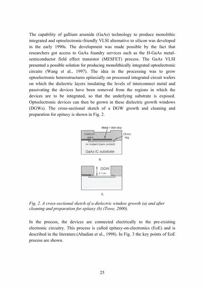
The capability of gallium arsenide (GaAs) technology to produce monolithic integrated and optoelectronic-friendly VLSI alternative to silicon was developed in the early 1990s. The development was made possible by the fact that researchers got access to GaAs foundry services such as the H-GaAs metal-semiconductor field effect transistor (MESFET) process. The GaAs VLSI presented a possible solution for producing monolithically integrated optoelectronic circuits (Wang et al., 1997). The idea in the processing was to grow optoelectronic heterostructures epitaxially on processed integrated circuit wafers on which the dielectric layers insulating the levels of interconnect metal and passivating the devices have been removed from the regions in which the devices are to be integrated, so that the underlying substrate is exposed. Optoelectronic devices can then be grown in these dielectric growth windows (DGWs). The cross-sectional sketch of a DGW growth and cleaning and preparation for epitaxy is shown in Fig. 2.
Fig. 2. A cross-sectional sketch of a dielectric window growth (a) and after cleaning and preparation for epitaxy (b) (Towe, 2000).
In the process, the devices are connected electrically to the pre-existing electronic circuitry. This process is called epitaxy-on-electronics (EoE) and is described in the literature.(Ahadian et al., 1998). In Fig. 3 the key points of EoE process are shown.
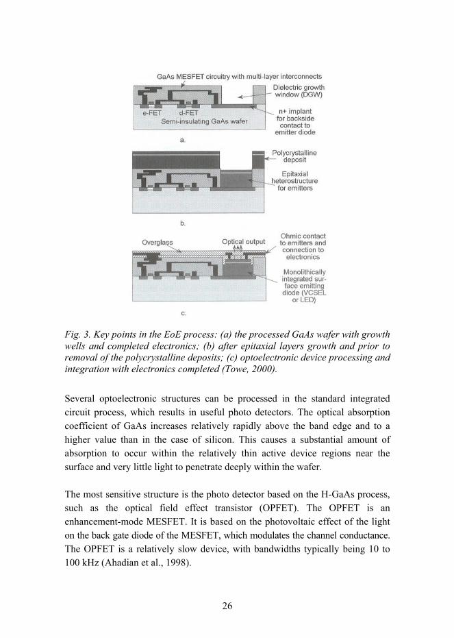
26
Fig. 3. Key points in the EoE process: (a) the processed GaAs wafer with growth wells and completed electronics; (b) after epitaxial layers growth and prior to removal of the polycrystalline deposits; (c) optoelectronic device processing and integration with electronics completed (Towe, 2000).
Several optoelectronic structures can be processed in the standard integrated circuit process, which results in useful photo detectors. The optical absorption coefficient of GaAs increases relatively rapidly above the band edge and to a higher value than in the case of silicon. This causes a substantial amount of absorption to occur within the relatively thin active device regions near the surface and very little light to penetrate deeply within the wafer.
The most sensitive structure is the photo detector based on the H-GaAs process, such as the optical field effect transistor (OPFET). The OPFET is an enhancement-mode MESFET. It is based on the photovoltaic effect of the light on the back gate diode of the MESFET, which modulates the channel conductance. The OPFET is a relatively slow device, with bandwidths typically being 10 to 100 kHz (Ahadian et al., 1998).
27
The much faster H-GaAs photo detector is a metal-semiconductor-metal (MSM) detector. It is made using the gate Schottky diode metal in an interdigitated finger pattern over a channel implant. In the standard H-GaAs process the exposed regions between the fingers are ion implanted with the source/drain implant dose which reduces the sensitivity of the detector significantly. Adding a masking step to the process to block the implant in these regions improves the MSM sensitivity. MSM photo detector bandwidth of 4 GHz is demonstrated. The commercial process, however, requires substantial additions to realize a high performance MSM photo detector (Giziewicz et al., 2004).
Monolithically integrated InGaP LEDs have been processed on GaAs substrates using epitaxy-on-electronics (EoE) technology (Hall et al., 1999). EoE technology has been applied to create a neural network based on smart pixel implementation. The experimental results demonstrate limitations in the performance of the detectors and LEDs for use in a full-scale implementation.
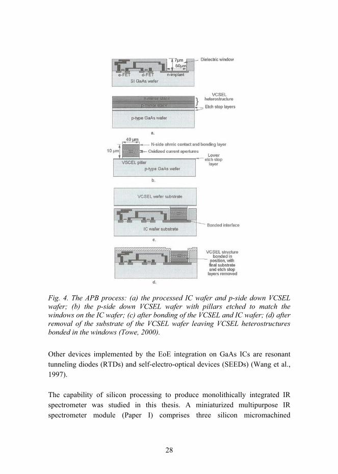
EoE integrated vertical-cavity surface-emitting lasers have not been actively pursued, because the focus has been instead on integrating VCSELs by aligned pillar bonding (APB) (Fonstad, 2001). It should be noticed that APB VCSELs involve the same processing after the heterostructures are bonded in the DGWs as do the EoE VCSELs after epitaxy and removal of the polycrystalline deposits. It seems that the technology developed for APB VCSEL processing will apply for EoE VCSELs as well. The main disadvantages of APB technology are lack of large GaAs or InP wafers and low efficiency in the use of the epitaxial material (Fonstad, 2001). In Fig. 4 the APB process is shown.
28
Fig. 4. The APB process: (a) the processed IC wafer and p-side down VCSEL wafer; (b) the p-side down VCSEL wafer with pillars etched to match the windows on the IC wafer; (c) after bonding of the VCSEL and IC wafer; (d) after removal of the substrate of the VCSEL wafer leaving VCSEL heterostructures bonded in the windows (Towe, 2000).
Other devices implemented by the EoE integration on GaAs ICs are resonant tunneling diodes (RTDs) and self-electro-optical devices (SEEDs) (Wang et al., 1997).
The capability of silicon processing to produce monolithically integrated IR spectrometer was studied in this thesis. A miniaturized multipurpose IR spectrometer module (Paper I) comprises three silicon micromachined

29
components: an electrically modulated thermal infrared emitter, an electrically tunable Fabry-Perot interferometer (FPI) and a photo detector. The infrared emitter and a photo detector are monolithically integrated into a silicon substrate. In addition, an integrated circuit (IC) chip is die-bonded and wire-bonded and an FPI flip-chip bonded on a silicon substrate.
The implemented IR spectrometer module can be considered to be an example of the achievable monolithic integration level of MOEMS using silicon processing. Source and detector are monolithically integrated to the substrate, but the system does not contain waveguide at all, but instead a free-space propagation path. In addition, the dispersive device is flip-chip bonded and the pre-amplifier chip is die-bonded to the substrate. Therefore, the implementation can be considered to be a quasi-hybrid or pseudo-monolithic.
The development of silicon processing technology has now enabled integration of the GSM/GPRS radio of a mobile phone on a single chip using 90 nm CMOS silicon technology, which makes the implementation extremely miniature and cost efficient (Muhammad et al., 2005). On the other hand, a fully monolithically integrated system containing photonic structures generating, manipulating and sensing light and implemented together with signal processing, computing and control sections into a single chip has not yet been successfully implemented, at least not for industrial applications.
The quasi-hybrid or pseudo-monolithic photonic integrated circuit is an intermediate between the monolithic and hybrid photonic integrated circuit (Nishihara et al., 1989). The pseudo-monolithic integration techniques so far combine all the best features of monolithic integration with the flexibility and universality of hybrid integration (Towe, 2000).
2.2 Hybrid integration
The hybrid integration of an optical interconnection system is possible to perform by processing a compound-semiconductor-based emitter and detector wafers and silicon-based complementary metal oxide semiconductor (CMOS) driving and processing electronics wafers in specific separate manufacturing processes. The devices on wafers are diced apart and the module integration is
30
possible to perform by bonding discrete devices on an electronic substrate, which is typically assembled in a metal casing. The electronic substrate and the casing are then equipped with needed optical, electrical, mechanical and thermal interconnections and encapsulation for the devices in the packaging process.
The possible electronic substrates used in the optical interconnections include flame retardant 4 (FR4) glass fiber reinforced epoxy, flexible polymer, printed electronics and low-temperature co-fired ceramics (LTCC) substrate. Typically, the same kind of assembly methods for devices to the substrates can be used, but the main characteristics of the substrates and possible applications can vary a lot. The FR4 substrate is commonly used in various electronics applications and its overall performance is good for optical interconnect and photonic applications. The more heat resistive material FR5 is also commercially available.
Flexible printed circuit polymer materials include polyimide (trade name Kapton), polyethylene, polyacrylate, polycarbonate and polyester. The operation temperature of polyimide is the highest, about 260°C and it is lead-free assembly process compatible. Polyimide foils can be used as electronic substrates with surface mount technology assembly systems.
Polytetrafluoroethylene (PTFE) is another high temperature polymer material and it can be reinforced with glass fiber. PTFE was originally developed by DuPond and its trade name is Teflon. Its properties start to degrade when temperature increases above 260°C. PTFE has excellent dielectric properties and it is used at high radio frequencies, making it suitable for use as an insulator in cables and connectors and as substrate material for microwave applications (Pal et al., 2005).
Liquid crystal polymer (LCP) material can also be utilized in electronic packages produced by injection molding. LCP polymer compounds combined with ancillary materials, such as metal lead frames and adhesives, which combine to produce a range of cavity package configurations that can compete in the same performance arena as ceramics (Ross, 2004).
Plastic-compatible printed conductor process using gold nanocrystals is demonstrated (Huang et al., 2003). The main advantage of using nanoparticles is that patterning of the substrates can be annealed at a low temperature. This
31
enables the use of very low-cost substrate materials in extremely cost-sensitive applications. The main difference compared to a traditional flexible substrate patterning is that additive processes such as gravure printing and inkjet instead of metallization patterning through lithography and etching can be utilized. The main advantages of the printed electronics substrates are high-speed production capability combined with low-cost and low-complexity manufacturing.
Low-temperature co-fired ceramics (LTCC) technology have typically been utilized to implement various radio frequency (RF) and microwave systems, such as a compact Bluetooth system module (Yeung et al., 2006) and a compact transmitter module for 62 GHz wireless terminals applications (Lee & Park, 2007). A wireless transceiver front-end including antenna operating at 56 GHz has also been implemented in LTCC technology (Pergola et al., 2007). The front-end is demonstrated with an optical interface in the application. The optical interface is implemented on a silicon motherboard and the modulated optical carrier is transmitted at 1.55 µm wavelength. The front-end module can be used in wireless local area networks, such as IEEE 802.11a or HIPERLAN2 requiring a direct link to an optical backbone. The main benefits of using LTCC in these applications have been multilayer integration capability, excellent metal conductivity, low attenuation characteristics and temperature coefficient of expansion of substrate material close to semiconductors such as silicon and GaAs.
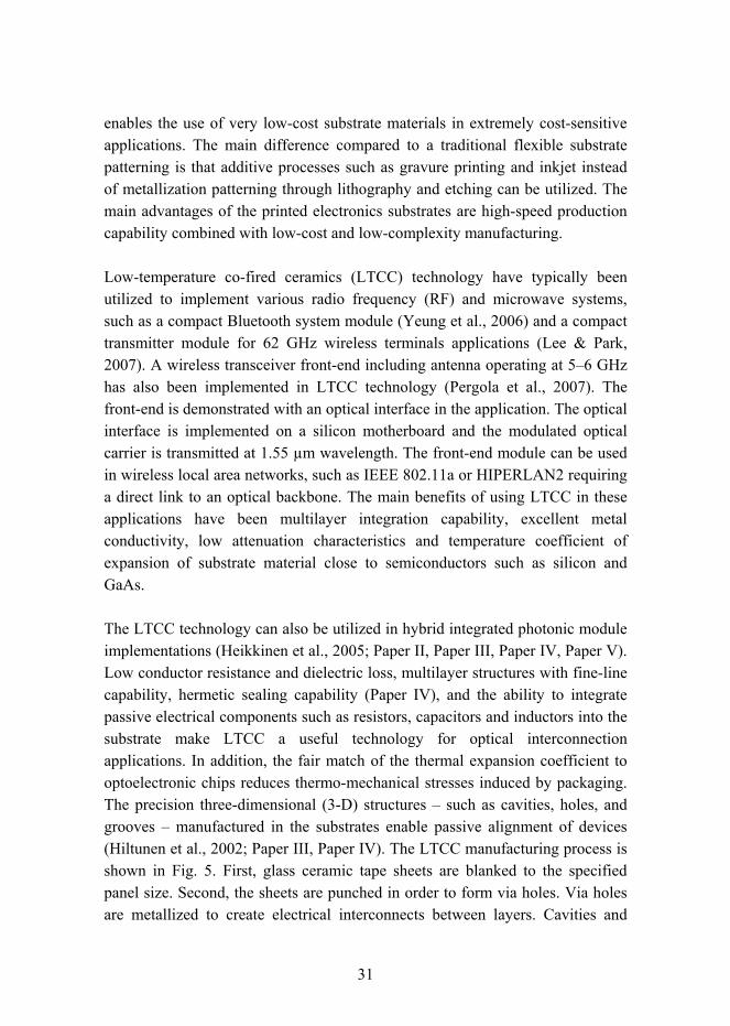
The LTCC technology can also be utilized in hybrid integrated photonic module implementations (Heikkinen et al., 2005; Paper II, Paper III, Paper IV, Paper V). Low conductor resistance and dielectric loss, multilayer structures with fine-line capability, hermetic sealing capability (Paper IV), and the ability to integrate passive electrical components such as resistors, capacitors and inductors into the substrate make LTCC a useful technology for optical interconnection applications. In addition, the fair match of the thermal expansion coefficient to optoelectronic chips reduces thermo-mechanical stresses induced by packaging. The precision three-dimensional (3-D) structures such as cavities, holes, and grooves manufactured in the substrates enable passive alignment of devices (Hiltunen et al., 2002; Paper III, Paper IV). The LTCC manufacturing process is shown in Fig. 5. First, glass ceramic tape sheets are blanked to the specified panel size. Second, the sheets are punched in order to form via holes. Via holes are metallized to create electrical interconnects between layers. Cavities and
32
grooves can be processed by via punching. The next step is patterning of electrical conductors and passive circuits onto each layer using screen-printing or photo imaging. The final steps are layer lamination, firing below a temperature of 980°C, processing of photo-imaged grooves and circuit dicing. Relatively low sintering temperature allows the use of noble metal conductor materials such as silver and gold.
Fig. 5. LTCC manufacturing process.
Fiber grooves can be processed by punching or by lithography using photosensitive materials to the substrates. The use of passive alignment in the production of hybrid integrated modules is especially advantageous in Volume production, due to the fact that the concept is simple and fast (Hunziker et al., 1995).
Silicon micromachining technologies that are used in the microelectronics industry are widely applied to tool high precision silicon substrates for passive alignment of fiber optic subassemblies. The accuracy of silicon substrates is adequate for the passive alignment of single mode photonic devices and components (Armiento et al., 1991; Sunaga et al., 2000; Uekawa et al., 2003).
Another possible technology for producing high precision structures with high aspect ratios and great structural heights with tight tolerances is LIGA (Malek & Saile, 2004). Classical LIGA technology based on x-ray deep-etch lithography is
33
characterized by aspect ratios up to 100, lateral features size of 1 µm and side wall surfaces as smooth as 50 nm of root mean square (RMS) roughness (Pantenburg et al., 1998). The LIGA process has been utilized to produce micro-optical benches for the passive alignment of devices (Muller et al., 1996; Schift and Söchtig, 1998) and mold inserts for fiber optic passive alignment substrate replication (Karioja et al., 2000). However, the high cost of the mask production for the LIGA master limits the application of LIGA to systems that are not cost-sensitive or are produced in a very large volume (Rode & Hillerich, 1999).
Medium and low volume production pursues methods with high flexibility and low processing cost. In order to meet the processing cost requirement for medium and low volume production of alignment substrates, a concept in which alignment grooves are embossed into metallic substrates has also been suggested (Rode & Hillerich, 1999).
The LTCC technology is applicable also to low and medium volume applications due to the fact that process-related initial and mask costs are typically moderate compared to silicon and LIGA processes (Paper III).
The LTCC panel manufacture and component assembly are realized using standard high Volume applicable production methods, such as screen printing, flip-chip assembly of devices and surface mount assembly and reflow soldering of discrete components. The use of standard high volume production methods enables competitive electronics integration on a hybrid platform comprising alignment structures for passive alignment of fiber and laser diode for high volume applications (Paper III, Paper IV).
The sub-section of hybrid integration technologies closer to monolithic integration than traditional hybrid integration is called heterogeneous optoelectronic integration. Heterogeneous integration attempts to develop basic technologies necessary for optical interconnections, which are based on wafer scale packaging (Towe, 2000). The basic idea in heterogeneous integration technology is the combination of silicon and photonic materials by epitaxy or by bonding (Jokerst et al., 2003). Material properties, such as crystal lattice structure and coefficient of thermal expansion (CTE), are critical for reliable heterogeneous integration. Typical epitaxy temperatures are 600°C and 750°C for GaAs by molecular beam epitaxy (MBE) and metal organic chemical vapor deposition (MOCVD),

34
respectively, and 1000°C, or more, for Si by chemical vapor deposition (CVD). It is obvious that the epitaxial layer will be under severe stress when the layer is cooled down to room temperature. The minimum thickness of the heterostructure layer of several hundred nanometers is needed for GaAs-based devices. On the other hand, a GaAs layer that is much more than a hundred nanometers thick cracks easily, when the wafer temperature has decreased from process temperature to room temperature.
If the material combination is made by bonding, the CTE problem still has to be solved. Wafers bonded together and heated or cooled several hundred degrees from the bonding temperature can confront destructively large stresses. As an example, if Si and GaAs wafers four inches in diameter are hydrophilically bonded together or even simply epoxied at room temperature and the temperature of the bonded pair is then increased, there will be significant stressing and bowing of the pair until one or both of the wafers breaks at approximately 335°C (London et al., 1999).
Functional amorphous silicon thin-film transistors have been processed on polyimide substrates (Hsu et al., 2002). This kind of development work can be considered to pave the way for heterogeneous integration based on the combination of polymer electronics substrate and epitaxial silicon tooling of signal processing electronics.
35
3. Manufacturing technologies for optics and opto-mechanics for photonic modules
3.1 Silicon surface micromachining
A silicon surface micromachining process, in which micro-optical devices are batch-fabricated on the surface of a silicon wafer, offers very promising production techniques for micro-optical devices and systems. The used production technologies typically employ the emerging micro-electro-mechanical-systems (MEMS) technologies. When MEMS technologies are used to implement optical components, the technology is called micro-opto-electro-mechanical-systems (MOEMS) (Wu, 1997).
Silicon surface micromachined optical components are intended to facilitate automated packaging of optoelectronic devices and subsystems, hence substantially lowering the overall packaging costs of products. Silicon-optical-bench (SOB) technology, commonly used to align optical systems on a silicon substrate using etched V-grooves, solder bumps, and other IC process derived techniques can be used to achieve +/- 1 µm transverse alignment tolerances (Cohen et al., 1992).
SOB technology can also be used for initial placement of the various optical components and devices in the module, followed by an automated active alignment procedure using micro mirrors, which are prefabricated on the silicon substrate using MEMS technologies (Muller & Lau, 1998).
A versatile manipulation of light is possible using surface silicon micro-machined components. Silicon surface micromachined Fabry-Perot resonators, which enable tunable spectral filtering, have been demonstrated (Tran et al., 1996). Silicon surface micromachined electrically tunable Fabry-Perot interferometer is the heart of CARBOCAP, the carbon dioxide sensor manufactured by Vaisala (Carson, 1997).
Comb drive micro mirrors for single-mode coupling and scanning systems have been demonstrated (Muller & Lau, 1998). A torsion vertical mirror, which has
36
been implemented for a 2x2 optical switch to be used in the reconfiguration of an optical network, has also been demonstrated (Lee et al., 1999).
3.2 Traditional and modern lens tooling
Traditional lens tooling utilizes milling, grinding and polishing of specific optical materials. The machining of optical materials with diamond tools for preparing surfaces for grinding and polishing is called milling. This is a collective term that is used to describe plano milling, curve generating, and more recently also the fine-milling done prior to high-speed polishing. Fine-milling operations have become important for the volume production of optics and they have replaced to a large degree the grinding with loose abrasives. Although more expensive tools and machines are required for fine-milling, these operations can be more cost-effective than abrasive grinding because of shorter work cycles and because several machines can be operated by the same operator (Karow, 2004).
Optical parts, which are almost always made of nonmagnetic materials, are generally wax blocked to a magnetic tool plate or to a nonmagnetic Pyrex blocking body held on the table by magnetic wedges. Stacked square or rectangular parts are usually waxed into metal jigs that are then magnetically held to the table. The loaded work piece table is manually moved underneath the raised up diamond wheel by a hand wheel or a power feed. While the table rotates, the diamond tool spindle is then lowered slowly until the wheel comes in contact with the work piece. After contact has been made, the diamond tool spindle is switched on and an aqueous coolant is supplied by a pump at a rate of 75 l/min. The tool spindle is then automatically lowered at a preselected feed rate to remove the desired amount of material (Karow, 2004).
Grinding is the process of shaping optical materials with free or loose abrasives. The abrasive powder is mixed with water and the grinding is done on grinding tools made of cast iron. The pregrinding and fine-grinding steps are now frequently replaced in volume production by finishing the glasses with diamond tools. For prototype lenses and low-volume production, free abrasive grinding continues to be widely used (Karow, 2004).
37
The final fabrication step in optical component tooling is polishing. The fine-ground surfaces become specular reflective and transparent during polishing. The optical surfaces attain their final shape at the same time. Metal polishing tools are covered with a viscoelastic material to which an aqueous slurry of a mildly abrasive polishing compound is applied (Karow, 2004).
The solution-gelatin (sol-gel) technique has been commercially in production of AR coatings since 1960s. The sol-gel technique consists of hydrolytic polycondensation of metal alkoxides to form 3D amorphous poly-networks of metal oxides through a gradual transition from a sol to a gel, that is, from a polymer or colloidal containing liquid to a solid state. The in situ transformation from liquid to solid is the most important requirement of the replication process. Nano-replication procedure for glass structures, which is capable of fabricating micro- and nano-scale features with diffraction gratings and Fresnel lenses have been demonstrated (Parashar et al., 2003). A thick micro lens fabrication using photosensitive sol-gel material has also been demonstrated (Yu & Yuan, 2003).
Although polishing optics using traditional methods is well established for spherical shape lenses, it is more difficult to polish parabolic or aspherical lens shapes. The use of aspherical lens profiles is advantageous in optical systems, because the amount of spherical aberration is decreased compared to spherical lenses, resulting in improved imaging quality. The improved image quality compared to spherical lenses is the main reason for applying aspherical lenses in implemented photonic module demonstrations (Paper II, Paper VI). Aspherical lens shapes can be tooled by a specific molding method similar to hot embossing (Maschmeyer et al., 1983, Sunohara et al., 1987). The process requires a specific molding tool, the temperature of which is warmed above glass transition temperature of the mold material. A pretooled glass piece is inserted between mold halves, which are then pressed towards each other, which induces compression to the pretooled piece and enforces its shape to the desired form. The method enables faster production speed of glass lenses than traditional lens machining (Sunohara et al., 1987; Yi et al., 2006).
The molding of glass materials typically requires clearly higher processing temperatures than thermoplastic materials. Glass molding has clearly higher tool costs due to more rapid wear of the tool compared to thermoplastic material molding in a volume production. The processing cycle in glass molding is
38
clearly longer than with thermoplastic molding. Method has, however, a competitive edge compared to diamond tool grinding, when glass material properties are required in a large volume application and plastic materials can not be applied.
3.3 Molding technologies
Molding technologies using thermoplastic polymers are efficient and cost-effective methods to fabricate optical parts (Michaeli & Wielpuetz, 2000). The fabrication cost of molded pieces is hardly affected by the complexity of the design. When the mold and insert have been tooled, tens of thousands pieces can be molded with a little effort. The raw materials cost is typically neglible, especially when the processed parts are miniature. Molding technologies enable production of pieces suitable for applications requiring very low-cost and disposable components (Heckele & Schomburg, 2004).
3.3.1 Molding technology variations
Injection molding is one of the widespread standard processes to fabricate polymer parts. It is used to form almost any geometry from a large variety of thermoplastic materials, and almost any plastic part with dimensions ranging from the millimeter to centimeter range can be manufactured with this technology. The fabrication of necessary mounting and assembly features, such as brackets and snap-fit-joints for component assembly in a one-shot molding process is possible (Michaeli & Wielpuetz, 2000).
The injection molding process starts with the raw polymer material, which is used in granular form. These granules are fed into a cylinder, a heated screw, where the grains start to melt. The melt is then transported towards the mold cavity. Typical temperatures in this region range from 200°C for polymers such as polymethyl methacrylate (PMMA) and polystyrene (PS) above 280°C for polymer like polycarbonate (PC) and up to 350°C for materials like polyetheretherketone (PEEK). The molten material is then injected under high pressure (6001000 bar) into the evacuated mold, which can contain a specific part to produce high precision features to the molded parts. When processing
39
macroscopic systems, the cavity can be held under the solidification temperature of the polymer and the so-called cold-cavity process is used. The mold is opened and the fabricated piece is ejected from the mold, when the piece has been solidified. The process allows rapid fabrication and the cycle times of some seconds are standard for most applications (Becker & Gärtner, 2000).
As the features become smaller, less material has to be injected into the cavity and the surface-to-volume ratio increases, and the cavity has to be heated closer to the melting point of polymer to allow the polymer to flow into all small features of the mold insert. The cavity will then be cooled to allow the ejection of micro-structured part. This process is called vario-therm and it allows manufacturing of smaller structures than cold-cavity process, but increases the cycle time due to the heating and cooling cycle. Typical cycle times of microinjection process are on the order of 1 to 3 minutes (Becker & Gärtner, 2000; Heckele & Schomburg, 2004).
There is a large gradient between injection and ejection temperature of the polymer as well as the phase transition between liquid and solid phase, and the resulting volume change and thermal shrinkage has to be taken into account in the insert and mold fabrication (Becker & Gärtner, 2000).
Sub-micrometer features down to 200 nm line width and 1:1 aspect ratio have been successfully processed by injection molding using several optical polymers. Best molding results were achieved, when the used melt and mold temperatures were high. The presented injection molding results indicate that grating periods between 0.8 µm to 1.6 µm can be replicated, which allows mass production of diffractive elements for the creation of different holographic effects (Mönkkönen et al., 2002).
Reaction injection molding is similar to injection molding, but instead of one type of plastic, two components are injected into the closed tool. This technique allows a use of materials that are not thermoplastic, such as thermosetting materials and elastomers. Earlier there were difficulties to achieve good mixture of components in micro scale and short cycle times. Now it is possible to use ultraviolet (UV) curing instead of thermal initiation of the polymerization, and reaction injection molding has appeared again. Today this process is quite fast
40
and allows a type of rapid prototyping because thermal cycling is not necessary any more (Heckele & Schomburg, 2004).
In the hot embossing process, the molding tool, the so-called insert, is pressed under a vacuum into a semi-finished polymer at a temperature above its glass temperature. Characteristics of this technology include comparably simple machines, low mechanical influences to the mold insert, the possibility to mold extremely small structures, the exact replication over large distances and the possibility to produce optical components (Heckele et al., 1998).
Hot embossing lithography is currently used for production of nanostructures as it has several advantages over other fabrication techniques. In this context the hot embossing is called nanoimprint technology. In comparison with optical lithography, it is not limited by the diffraction limit and thin resist layers can be patterned down to 10 nm (Chou et al., 1997). The method is fast, when compared to electron beam (EB) and scanning probe microscopy (SPM) lithography and cost-efficient when compared to x-ray lithography (Heyderman et al., 2000).
3.3.2 Thermoplastic materials
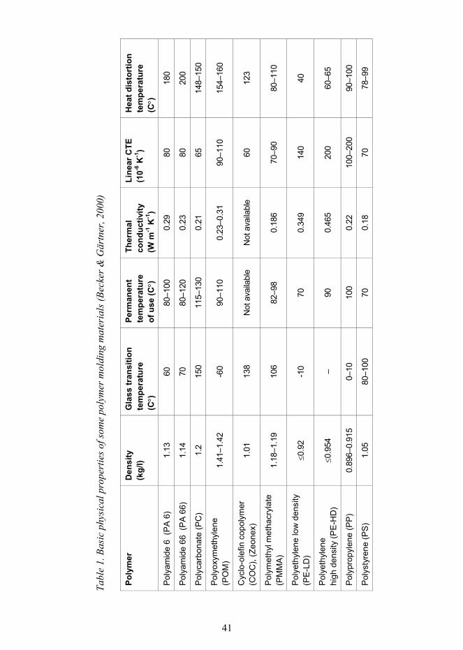
Thermoplastic polymers are a very large material group, which contains suitable polymer candidates for almost every application. There are materials, which are stable at temperatures as high as 250°C, such as PEEK and some polymers which resist aggressive chemicals such as alkaline solutions, acids, and solvents like perfluoralkoxy (PFA). Polymers are electrical and thermal insulators, but when filled with proper powders they can be used as conductors and heat sinks. Molded pieces can be soft and elastic as polyoxymethylene (POM) or hard and brittle like polysulfone (PSU). They are available from optically transparent as cyclo-olefin copolymer (COC) and opaque like polyamide (PA) filled with graphite (Heckele & Schomburg, 2004). Basic physical properties of some polymer molding materials are shown in Table 1.
Tabl
e 1.
Bas
ic p
hysi
cal p
rope
rtie
s of s
ome
poly
mer
mol
ding
mat
eria
ls (B
ecke
r & G
ärtn
er, 2
000)
Poly
mer
D
ensi
ty
(kg/
l) G
lass
tran
sitio
n te
mpe
ratu
re
(C°)
Perm
anen
t te
mpe
ratu
re
of u
se (C
°)
Ther
mal
co
nduc
tivity
(W
m-1
K-1
)
Line
ar C
TE
(10-6
K-1
) H
eat d
isto
rtio
n te
mpe
ratu
re
(C°)
Pol
yam
ide
6 (P
A 6
) 1.
13
60
801
00
0.29
80
18
0
Pol
yam
ide
66 (
PA
66)
1.
14
70
801
20
0.23
80
20
0
Pol
ycar
bona
te (P
C)
1.2
150
115
130
0.21
65
14
815
0
Poly
oxym
ethy
lene
(P
OM
) 1.
411
.42
-60
901
10
0.23
0.3
1 90
110
15
416
0
Cyc
lo-o
lefin
cop
olym
er
(CO
C),
(Zeo
nex)
1.
01
138
Not
ava
ilabl
e N
ot a
vaila
ble
60
123
Pol
ymet
hyl m
etha
cryl
ate
(PM
MA
) 1.
181
.19
106
829
8 0.
186
709
0 80
110
Pol
yeth
ylen
e lo
w d
ensi
ty
(PE
-LD
) ≤0
.92
-10
70
0.34
9 14
0 40
Pol
yeth
ylen
e
high
den
sity
(PE
-HD
) ≤0
.954
90
0.46
5 20
0 60
65
Pol
ypro
pyle
ne (P
P)
0.89
60.
915
010
10
0 0.
22
100
200
901
00
Pol
ysty
rene
(PS
) 1.
05
801
00
70
0.18
70
78
99
41
42
The main disadvantages of polymer materials in photonics applications compared to silicon, glass and ceramic materials are lower heat distortion temperature, larger CTE, moisture absorption, a tendency to creep and diffusion of gases (Heckele & Schomburg, 2004).
3.3.3 Tool manufacturing technologies
The tool for replication is typically called a mold. The two main technologies for mold manufacturing are traditional mechanical machining using modern computer numerical control (CNC) multi-axis machines with diamond tools and electric discharge machining (EDM). An integrated part of the mold, the function of which is to replicate high precision and minute features in the molding process, is called an insert. The insert can be manufactured by diamond tooling technologies (Bäumer, 2005) and by several lithographic technologies like, optical, x-ray (Heckele & Schomburg, 2004) and electron beam (EB) lithography (Mönkkönen et al. 2002). The current EB lithography is able to tool sub-10 nm features, but the processing of large areas is time consuming.
Lithographic processes are particularly suited for minute structures. A resist is patterned with a micro-structure that is electroplated to build up a mold insert. A novel LIGA technique for resist exposure capable of producing 3D microstructures has been demonstrated. The technique has been applied to fabricate PMMA microlens arrays for micro-optic application and micro needles for bio-medical applications. The measured RMS surface roughness of the fabricated pieces has been 10 nm (Sugiyama et al., 2004).
Laser machining can also be used in fabrication of the insert. The laser technology is of particular interest, as it allows tooling of stainless steel and tungsten carbide, which are very difficult to tool using previously mentioned technologies and diamond tooling (Heckele & Schomburg, 2004).
Diamond tooling of the insert is actually the final manufacturing phase to produce a high precision surface with a low surface roughness to a nickel coated surface on a steel insert. Measured RMS surface roughness of nickel coated insert has been 56 nm and the surface roughnesses of replicated lenses have been at the same level (Paper VI). A nickel layer is required on the top of the
43
steel due to the fact that the diamond tool wears very rapidly when being in contact with the carbon in the steel during the tooling process. The normal procedure to fabricate an insert is to pre-tool the insert using a traditional CNC multi-axis machine, so that the coating layer thickness is observed in the tooling. The insert surface is coated next with nickel and finally tooled to the accurate profile by diamond tooling. It is a very substantial characteristic of diamond tooling that an aspheric surface profile is possible to tool as easily as a spherical surface to the insert. There are some companies, such as Rochester Precision Optics in USA and Juken in Japan, offering nickel coating and diamond tooling services for the insert fabrication.
Mold inserts from glass or silicon substrates, which can be lithographically patterned using wet etching or reactive ion etching (RIE), can be also used in molding, but the silicon is a very brittle material and the wafers tend to break. Therefore the wafer is bonded on the top of quartz glass to get a stable compound. If less than ten molding cycles are performed for prototyping purposes, mold inserts made from silicon may be suitable. Silicon treated by wet-etching is more favorable, because it shows inclined side walls and a smoother surface than dry-etched silicon (Heckele & Schomburg, 2004).
3.4 Polymer encapsulation of electronics and integration with mechanics and optics using injection molding
A very cost-effective mass production method to encapsulate electronic substrates by polymers using injection molding has been developed for the manufacture of plastic automotive components with embedded electronics and power distribution (Teh et al., 2000). The electronic sub-systems are simultaneously packaged within the automotive structural thermoplastic component during the injection molding process. The process and product integration represents an opportunity to significantly reduce component counts and wiring loom overhead for the vehicle. The assembly, weight and cost advantages envisaged from the proposed technology is suggested to satisfy the ever increasing demand for automotive suppliers to manufacture complete, ready-to-assemble, reconfigurable component modules with superior reliability and as such may contribute to the increasing incorporation of vehicle telematics (Teh et al., 2000).
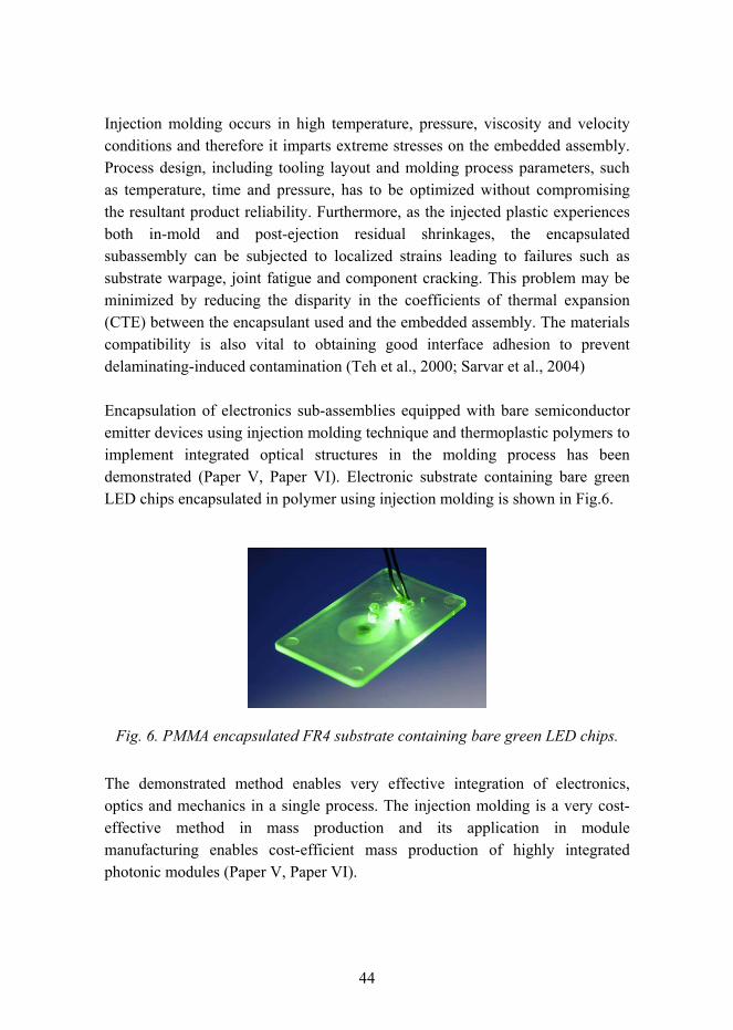
44
Injection molding occurs in high temperature, pressure, viscosity and velocity conditions and therefore it imparts extreme stresses on the embedded assembly. Process design, including tooling layout and molding process parameters, such as temperature, time and pressure, has to be optimized without compromising the resultant product reliability. Furthermore, as the injected plastic experiences both in-mold and post-ejection residual shrinkages, the encapsulated subassembly can be subjected to localized strains leading to failures such as substrate warpage, joint fatigue and component cracking. This problem may be minimized by reducing the disparity in the coefficients of thermal expansion (CTE) between the encapsulant used and the embedded assembly. The materials compatibility is also vital to obtaining good interface adhesion to prevent delaminating-induced contamination (Teh et al., 2000; Sarvar et al., 2004)
Encapsulation of electronics sub-assemblies equipped with bare semiconductor emitter devices using injection molding technique and thermoplastic polymers to implement integrated optical structures in the molding process has been demonstrated (Paper V, Paper VI). Electronic substrate containing bare green LED chips encapsulated in polymer using injection molding is shown in Fig.6.
Fig. 6. PMMA encapsulated FR4 substrate containing bare green LED chips.
The demonstrated method enables very effective integration of electronics, optics and mechanics in a single process. The injection molding is a very cost-effective method in mass production and its application in module manufacturing enables cost-efficient mass production of highly integrated photonic modules (Paper V, Paper VI).
45
4. Photonic module integration demonstrators
4.1 Miniature infrared spectrometer
The objective of this work was to demonstrate the capabilities of surface silicon micromechanics design and manufacturing tools in the implementation of micro-optical electro-mechanical systems (MOEMS) and evaluate the feasibility of a monolithically integrated sensor system.
4.1.1 Devices and operational principle of the spectrometer
A miniaturized multipurpose IR spectrometer module (Paper I), comprises of three silicon micro machined devices: an electrically modulated thermal infrared emitter, an electrically tunable Fabry-Perot interferometer (FPI) and a photo detector.
The size of the infrared emitter is 1 mm x 1 mm. The emitter consists of several emitting wires with 1-µm thickness, 20-µm width and 1000-µm length. The operating temperature of the emitter is about 1000 K.
The silicon micro machined FPI device (Pat. US 5,561,523, 1996) is an optical resonator consisting of two parallel highly reflective mirrors separated by a cavity. The transmission band of the device is controlled by electrically changeable gap between the mirrors. The structure of the FPI device is shown in Fig. 7. The size of the FPI chip is 3.3 mm x 3.3 mm x 0.5 mm. The active area diameter is 0.75 mm. The typical transmission of the FPI is 65% and the typical FWHM band pass 70 nm, when Numerical Aperture (NA) of 0.2 is used. A 20% tuning range of the nominal wavelength, 95% transmission and a 25 dB contrast can be obtained.
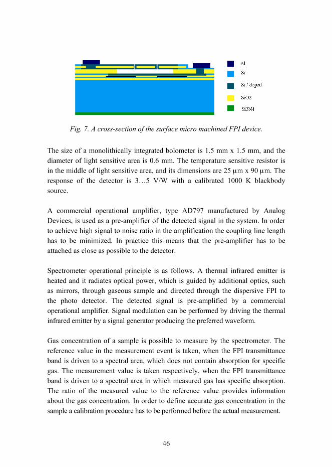
46
Fig. 7. A cross-section of the surface micro machined FPI device.
The size of a monolithically integrated bolometer is 1.5 mm x 1.5 mm, and the diameter of light sensitive area is 0.6 mm. The temperature sensitive resistor is in the middle of light sensitive area, and its dimensions are 25 µm x 90 µm. The response of the detector is 35 V/W with a calibrated 1000 K blackbody source.
A commercial operational amplifier, type AD797 manufactured by Analog Devices, is used as a pre-amplifier of the detected signal in the system. In order to achieve high signal to noise ratio in the amplification the coupling line length has to be minimized. In practice this means that the pre-amplifier has to be attached as close as possible to the detector.
Spectrometer operational principle is as follows. A thermal infrared emitter is heated and it radiates optical power, which is guided by additional optics, such as mirrors, through gaseous sample and directed through the dispersive FPI to the photo detector. The detected signal is pre-amplified by a commercial operational amplifier. Signal modulation can be performed by driving the thermal infrared emitter by a signal generator producing the preferred waveform.
Gas concentration of a sample is possible to measure by the spectrometer. The reference value in the measurement event is taken, when the FPI transmittance band is driven to a spectral area, which does not contain absorption for specific gas. The measurement value is taken respectively, when the FPI transmittance band is driven to a spectral area in which measured gas has specific absorption. The ratio of the measured value to the reference value provides information about the gas concentration. In order to define accurate gas concentration in the sample a calibration procedure has to be performed before the actual measurement.

47
4.1.2 System optical modeling
The system optical modeling was concentrated on the most critical characteristics of the spectrometer system, which were throughput, optical crosstalk and usable numerical aperture (NA) of the system. The aim of the optical modeling was to optimize the systems performance. An analytical modeling results achieved by MathCAD were compared to the ray trace model achieved by Advanced System Analyzation Program (ASAP).
A throughput value of an optical system is defined to be
Ω= AT , (1)
where A is the limiting transmitting element area and Ω is the solid angle. In order to estimate optical throughput and resulting signal from the source to the detector, an analytical model of the system was derived treating the thermal infrared emitter as a graybody radiator (McCluney, 1994).
The total radiant flux emitted by the thermal source is depending of the source absolute temperature. The total radiant flux emitted from the surface of a graybody radiator at this temperature can be expressed by the Stefan-Boltzmann law, as
4TM bb εσ= , (2)
where Mbb is the exitance of the emitter surface in vacuum, ε is emissivity of the radiator, σ is the Stefan-Boltzmanns constant, and T is the temperature of the source in Kelvin. A blackbody at 973 K emits at the rate of 50823 W/m2.
The Plancks blackbody spectral radiation law accurately predicts the spectral radiance of blackbodies in vacuum at any temperature in the form
)1(
2
5
2
−=
Thcbb
e
hcLλσ
λ
λ
ε, (3)

48
where h is the Plancks constant, c is the speed of light in vacuum, and λ is the wavelength.
Inserting the values of the constants into equation 3 and multiplying by π, λ in µm, we get spectral exitance of the emitter
)1(10741.3
/143885
428
−×××
= ×
−
TKmbb emmWM λµλ λµ
, (4)
If the specific wavelength is 4.5 µm, then the spectral exitance of the emitter is 7845 W×m-2×µm-1. By assuming emitter area to be circular, the size of which is the same as that of the detector, we get 0.16 mW at 70 nm wavelength band. It is possible to collect about 2% of the IR emitters total radiant power and transmit it to the detector by the optics, when the IR emitter is approximated to a point source and ideal optics is used. If the FPI transmittance is 65%, the detector response 5 V/W and the Voltage amplification 570, then the signal value will be 5.9 mV.
According to ray trace simulations, the optical throughput from the source to the detector was 0.4% without a cover. Approximation with a point source with an ideal optics gave the efficiency of 2%. The spherical aberration of a mirror and the fact that the transmission losses had been ignored in the analytical modeling were the main causes of this discrepancy.
The obtained level of a normalized optical crosstalk value was 1:12000 at the maximum in ray trace simulation. The main part of the stray light was origin from the emitter coupled via silicon substrate to the detector. A gap was etched to the substrate next to the emitter to block most of the substrate coupled rays.
In order to estimate the effect of the incident light angular distribution on the surface of the FPI, the analytical model of the FPI transmittance as a function of angular distribution was created. The FPI transmission spectrum for a plane wave is the following (Hecht, 1990)

49
22
22
)cos(2(sin(4)1(
)1()1(
1
),,,,,(
⎥⎦⎤
⎢⎣⎡++−
+−⎥⎦
⎤⎢⎣
⎡−
−
=
λθπ
θλ
ndRR
RR
A
nARdTFPI
(5)
and the transmission in a converging beam is
∫
∫
=
max
max
0
0
max
2
2),,,,,(
),,,,,(
θ
θ
θ
θπθ
θπθθλ
θλ
d
dnARdT
nARdT
FPI
FPI
. (6)
The calculated average transmission of the FPI, when a converging beam half angle θmax is 0.1° (NA≈1.7 × 10⁻³), 5.7° (NA≈0.1), 11.5° (NA≈0.2) and 17.5° (NA≈0.3), is shown in Fig. 8.
Fig. 8. Calculated average transmittance of the FPI, when the beam half angle θmax is 0.1°, 5.7°, 11.5° and 17.5°.
As it can be seen from Fig. 8, when the converging beam half angle increases, the transmission peak lowers, broadens and moves towards shorter wavelengths. The selectivity of the measurement system increases when NA is decreasing, but
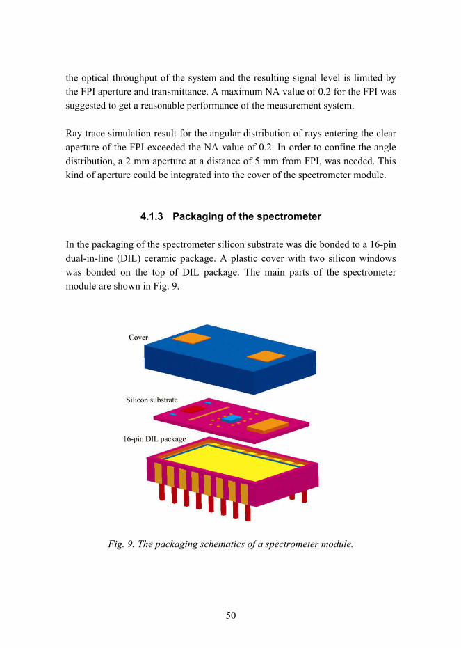
50
the optical throughput of the system and the resulting signal level is limited by the FPI aperture and transmittance. A maximum NA value of 0.2 for the FPI was suggested to get a reasonable performance of the measurement system.
Ray trace simulation result for the angular distribution of rays entering the clear aperture of the FPI exceeded the NA value of 0.2. In order to confine the angle distribution, a 2 mm aperture at a distance of 5 mm from FPI, was needed. This kind of aperture could be integrated into the cover of the spectrometer module.
4.1.3 Packaging of the spectrometer
In the packaging of the spectrometer silicon substrate was die bonded to a 16-pin dual-in-line (DIL) ceramic package. A plastic cover with two silicon windows was bonded on the top of DIL package. The main parts of the spectrometer module are shown in Fig. 9.
Fig. 9. The packaging schematics of a spectrometer module.
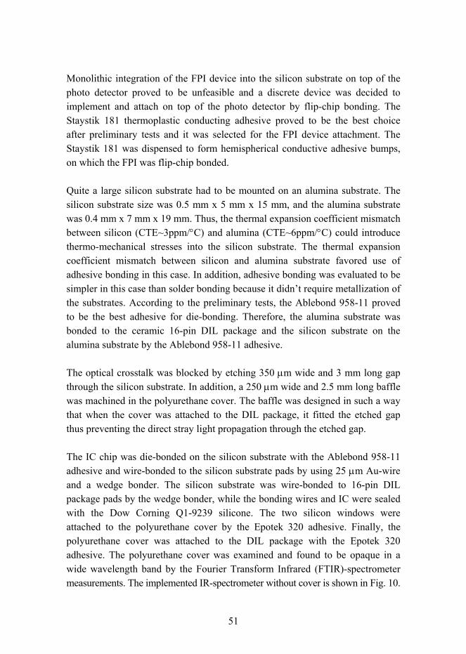
51
Monolithic integration of the FPI device into the silicon substrate on top of the photo detector proved to be unfeasible and a discrete device was decided to implement and attach on top of the photo detector by flip-chip bonding. The Staystik 181 thermoplastic conducting adhesive proved to be the best choice after preliminary tests and it was selected for the FPI device attachment. The Staystik 181 was dispensed to form hemispherical conductive adhesive bumps, on which the FPI was flip-chip bonded.
Quite a large silicon substrate had to be mounted on an alumina substrate. The silicon substrate size was 0.5 mm x 5 mm x 15 mm, and the alumina substrate was 0.4 mm x 7 mm x 19 mm. Thus, the thermal expansion coefficient mismatch between silicon (CTE~3ppm/°C) and alumina (CTE~6ppm/°C) could introduce thermo-mechanical stresses into the silicon substrate. The thermal expansion coefficient mismatch between silicon and alumina substrate favored use of adhesive bonding in this case. In addition, adhesive bonding was evaluated to be simpler in this case than solder bonding because it didnt require metallization of the substrates. According to the preliminary tests, the Ablebond 958-11 proved to be the best adhesive for die-bonding. Therefore, the alumina substrate was bonded to the ceramic 16-pin DIL package and the silicon substrate on the alumina substrate by the Ablebond 958-11 adhesive.
The optical crosstalk was blocked by etching 350 µm wide and 3 mm long gap through the silicon substrate. In addition, a 250 µm wide and 2.5 mm long baffle was machined in the polyurethane cover. The baffle was designed in such a way that when the cover was attached to the DIL package, it fitted the etched gap thus preventing the direct stray light propagation through the etched gap.
The IC chip was die-bonded on the silicon substrate with the Ablebond 958-11 adhesive and wire-bonded to the silicon substrate pads by using 25 µm Au-wire and a wedge bonder. The silicon substrate was wire-bonded to 16-pin DIL package pads by the wedge bonder, while the bonding wires and IC were sealed with the Dow Corning Q1-9239 silicone. The two silicon windows were attached to the polyurethane cover by the Epotek 320 adhesive. Finally, the polyurethane cover was attached to the DIL package with the Epotek 320 adhesive. The polyurethane cover was examined and found to be opaque in a wide wavelength band by the Fourier Transform Infrared (FTIR)-spectrometer measurements. The implemented IR-spectrometer without cover is shown in Fig. 10.
52
Fig. 10. IR-spectrometer.
4.1.4 Characterization of the spectrometer module
In the measurements biasing electronics, operating voltage electronics and filtering electronics were placed on a FR4 board, which also contained a base for the 16-pin DIL spectrometer module. Thermal source was driven by 50/50 square pulses at a frequency band from 0.1.Hz to 20 Hz. The heating and cooling process was time consuming, which limited the upper practical modulation frequency at the level of a one hundred hertz. A spherical mirror was used to couple light from the source to the detector through the dispersive FPI device. The signal was amplified and measured by a phase-locked amplifier.
The simulated transmission value of the system was 0.4% and FPI transmission 0.65, which would give 1.2 mV signal level as a result. When modulating the source at 5 Hz, the detected module signal level at a reference band was 1 mV and peak-to-peak noise level was 10 µV, resulting in a 100 signal-to-noise ratio at 1 Hz bandwidth. Thus, the measured signal value was 83% of the ray trace signal value, which is in a good agreement with the simulation.
The detected signal contained about a 3 mV offset level when the source was modulated at the 0.1 ... 20 Hz frequency band. The offset level was due to electrical crosstalk of the system. Crosstalk coupling from the emitter circuitry to the detector electronics seemed to be capacitive coupling via the silicon
53
substrate. The electrical crosstalk could be attenuated about 30 dB by using sine wave modulation of the source instead of square wave modulation.
4.1.5 Evaluation of the spectrometer implementation
The implemented IR-spectrometer module can be considered to be example of the achievable monolithic integration level of MOEMS using silicon surface micromachining. The thermal emitter and photo detector were monolithically integrated to the silicon substrate, but the FPI was flip-chip bonded and pre-amplifier IC was die-bonded, meaning that they were hybrid integrated, to the module.
The thermal emitter upper modulation frequency was limited to one hundred hertz, which denotes that the measuring speed of the system was moderate. In addition, the thermal source life time was typically much shorter than achieved with compound semiconductor technology emitters.
The fill factor of the substrate was low and the size of the substrate was relatively large, which highly compromised the system cost-efficiency. The optical cross talk was attenuated in a very low level by etching gap and inserting a baffle in the system, but a considerable amount of electrical cross talk was still measured in the implemented system.
The substrate was assembled into a ceramic package, which is hermetic material, but the gas is capable to penetrate through polyurethane cover. It could be advantageous to utilize novel polymer blends, which effectively limit the gas penetration into the sensor module package. That kind of material technology, however, was not available at the time of the system packaging.
As a conclusion, the system implementation proved that a complete monolithic integration of optical functions and driving and signal processing electronics on a single silicon chip was not practical using silicon surface micromachining technologies.
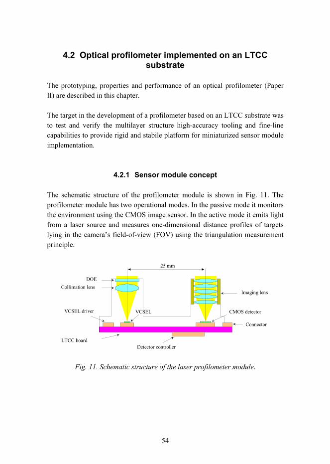
54
4.2 Optical profilometer implemented on an LTCC substrate
The prototyping, properties and performance of an optical profilometer (Paper II) are described in this chapter.
The target in the development of a profilometer based on an LTCC substrate was to test and verify the multilayer structure high-accuracy tooling and fine-line capabilities to provide rigid and stabile platform for miniaturized sensor module implementation.
4.2.1 Sensor module concept
The schematic structure of the profilometer module is shown in Fig. 11. The profilometer module has two operational modes. In the passive mode it monitors the environment using the CMOS image sensor. In the active mode it emits light from a laser source and measures one-dimensional distance profiles of targets lying in the cameras field-of-view (FOV) using the triangulation measurement principle.
DOECollimation lens
CMOS detector
Imaging lens
VCSEL driver
Detector controllerLTCC board
Connector
VCSEL
25 mm
Fig. 11. Schematic structure of the laser profilometer module.
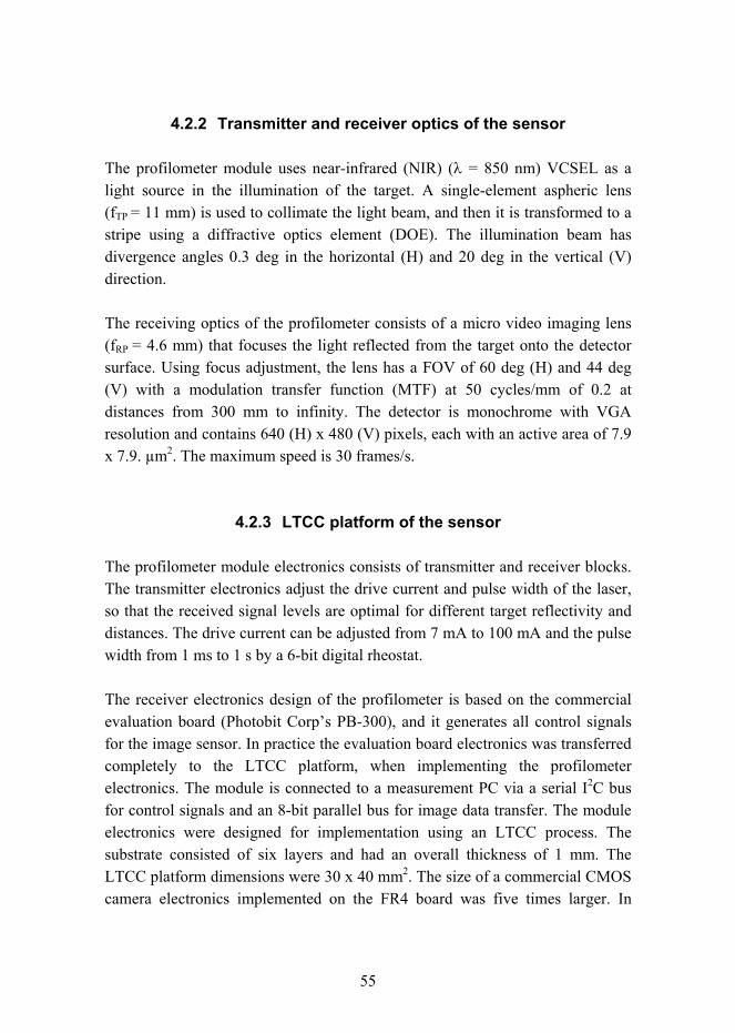
55
4.2.2 Transmitter and receiver optics of the sensor
The profilometer module uses near-infrared (NIR) (λ = 850 nm) VCSEL as a light source in the illumination of the target. A single-element aspheric lens (fTP = 11 mm) is used to collimate the light beam, and then it is transformed to a stripe using a diffractive optics element (DOE). The illumination beam has divergence angles 0.3 deg in the horizontal (H) and 20 deg in the vertical (V) direction.
The receiving optics of the profilometer consists of a micro video imaging lens (fRP = 4.6 mm) that focuses the light reflected from the target onto the detector surface. Using focus adjustment, the lens has a FOV of 60 deg (H) and 44 deg (V) with a modulation transfer function (MTF) at 50 cycles/mm of 0.2 at distances from 300 mm to infinity. The detector is monochrome with VGA resolution and contains 640 (H) x 480 (V) pixels, each with an active area of 7.9 x 7.9. µm2. The maximum speed is 30 frames/s.
4.2.3 LTCC platform of the sensor
The profilometer module electronics consists of transmitter and receiver blocks. The transmitter electronics adjust the drive current and pulse width of the laser, so that the received signal levels are optimal for different target reflectivity and distances. The drive current can be adjusted from 7 mA to 100 mA and the pulse width from 1 ms to 1 s by a 6-bit digital rheostat.
The receiver electronics design of the profilometer is based on the commercial evaluation board (Photobit Corps PB-300), and it generates all control signals for the image sensor. In practice the evaluation board electronics was transferred completely to the LTCC platform, when implementing the profilometer electronics. The module is connected to a measurement PC via a serial I2C bus for control signals and an 8-bit parallel bus for image data transfer. The module electronics were designed for implementation using an LTCC process. The substrate consisted of six layers and had an overall thickness of 1 mm. The LTCC platform dimensions were 30 x 40 mm2. The size of a commercial CMOS camera electronics implemented on the FR4 board was five times larger. In
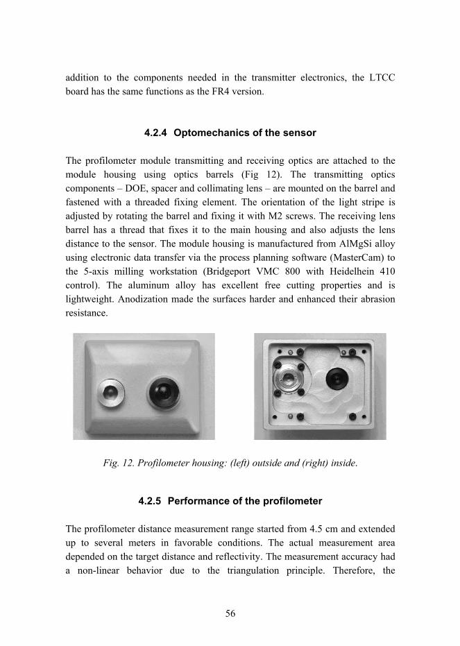
56
addition to the components needed in the transmitter electronics, the LTCC board has the same functions as the FR4 version.
4.2.4 Optomechanics of the sensor
The profilometer module transmitting and receiving optics are attached to the module housing using optics barrels (Fig 12). The transmitting optics components DOE, spacer and collimating lens are mounted on the barrel and fastened with a threaded fixing element. The orientation of the light stripe is adjusted by rotating the barrel and fixing it with M2 screws. The receiving lens barrel has a thread that fixes it to the main housing and also adjusts the lens distance to the sensor. The module housing is manufactured from AlMgSi alloy using electronic data transfer via the process planning software (MasterCam) to the 5-axis milling workstation (Bridgeport VMC 800 with Heidelhein 410 control). The aluminum alloy has excellent free cutting properties and is lightweight. Anodization made the surfaces harder and enhanced their abrasion resistance.
Fig. 12. Profilometer housing: (left) outside and (right) inside.
4.2.5 Performance of the profilometer
The profilometer distance measurement range started from 4.5 cm and extended up to several meters in favorable conditions. The actual measurement area depended on the target distance and reflectivity. The measurement accuracy had a non-linear behavior due to the triangulation principle. Therefore, the
57
measurement resolution corresponding to one pixel varied from 1 mm in short ranges to 1 cm at a distance of 1 m. According to the test results, distance profiles could be obtained from 100 points with accuracy (standard deviation) varying from 0.1 mm at a distance of 5 cm, to 2 cm at a distance of 1.5 m. An example of distance profile measurement presented using the graphical overlay is shown in Fig. 13. Here the corner of a card box was used as a target. The middle section of the laser stripe is marked with a gray line. The results shown here correspond to detector rows from 140 to 290 with a 10-row increment.
Fig. 13. Distance profile measurement of the cardboard box.
The image quality of the sensor was determined using an MTF test chart (Sine Patterns M-13-60, 4X version). The sensor was able to distinguish features with the dimensions on the order of 1 mm at a distance of 200 mm.
4.2.6 Evaluation of the profilometer implementation
The multilayer LTCC technology, combined with the possibility of integrating passive electrical components and alignment features into the substrate, clearly reduced the size of the circuit board. This opens up new possibilities to use the sensor in portable devices where small size, light weight, and low power consumption are important. The LTCC substrate offered a rigid and stable platform for profilometer implementation.
58
The laser and detector were attached to the LTCC substrate under the microscope with a lateral inaccuracy of ±0.03 mm. The 5-axis precision machine tool manufactured the housing structure with a dimensional tolerance of ±0.02 mm. The holes in the LTCC substrate, drilled by an Nd:YAG laser, had a centering inaccuracy of ±0.03 and a diameter tolerance of ±0.02 mm. So the achieved lateral positioning inaccuracy was better than ±0.1 in the alignment of the active photonic components.
The profilometer characterization proved that the module mainly operated as designed. The poor quality of the beam-spreading element limited the useful portion of the laser stripe to about one-third of the detector height. This limited the number of profile measurement points. It was naturally possible to acquire and assemble a high quality beam-spreading element into the module, but the system performance was still well adequate to demonstrate the LTCC substrate advantages for miniature distance sensor implementations. The one drawback of using LTCC substrate in this case was that repairing of the prototype boards was seen to be more difficult than epoxy fiberglass PCBs due to the rugged nature of the ceramic material. It was also noticed that targets with strong specular reflectance sometimes caused incorrect distance measurement results, which are common to triangulation sensors using laser spot or stripe illumination.
As a conclusion, the module implementation demonstrated that it is possible to utilize LTCC substrate as an accurate optomechanical platform for miniature sensor modules for portable devices.
4.3 Passive alignment laser modules based on an LTCC substrate
The capabilities of low-temperature co-fired ceramics technology tooling to produce passive alignment of devices were developed and tested in this work (Paper III, Paper IV). In addition, the ceramics technology capability to supply hermetic package for a fiber pigtailed laser module using substrate as an integral part of the package was verified (Paper IV).
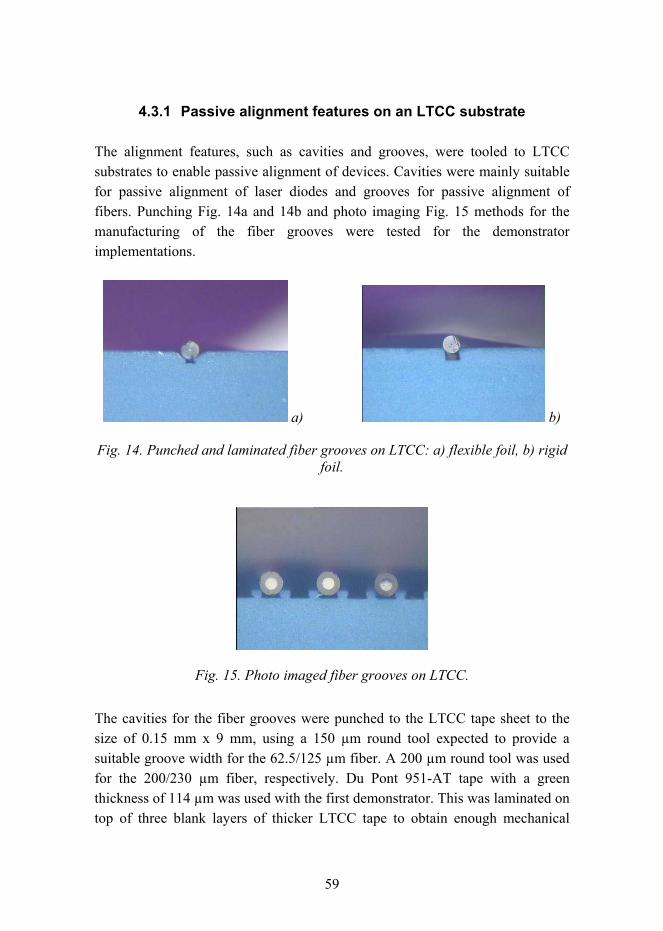
59
4.3.1 Passive alignment features on an LTCC substrate
The alignment features, such as cavities and grooves, were tooled to LTCC substrates to enable passive alignment of devices. Cavities were mainly suitable for passive alignment of laser diodes and grooves for passive alignment of fibers. Punching Fig. 14a and 14b and photo imaging Fig. 15 methods for the manufacturing of the fiber grooves were tested for the demonstrator implementations.
a) b)
Fig. 14. Punched and laminated fiber grooves on LTCC: a) flexible foil, b) rigid foil.
Fig. 15. Photo imaged fiber grooves on LTCC.
The cavities for the fiber grooves were punched to the LTCC tape sheet to the size of 0.15 mm x 9 mm, using a 150 µm round tool expected to provide a suitable groove width for the 62.5/125 µm fiber. A 200 µm round tool was used for the 200/230 µm fiber, respectively. Du Pont 951-AT tape with a green thickness of 114 µm was used with the first demonstrator. This was laminated on top of three blank layers of thicker LTCC tape to obtain enough mechanical
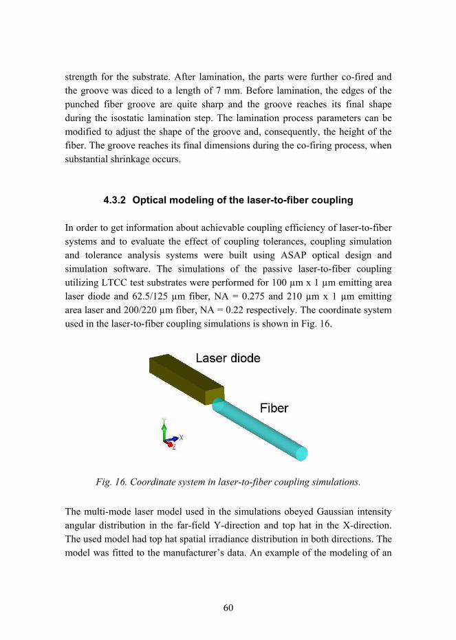
60
strength for the substrate. After lamination, the parts were further co-fired and the groove was diced to a length of 7 mm. Before lamination, the edges of the punched fiber groove are quite sharp and the groove reaches its final shape during the isostatic lamination step. The lamination process parameters can be modified to adjust the shape of the groove and, consequently, the height of the fiber. The groove reaches its final dimensions during the co-firing process, when substantial shrinkage occurs.
4.3.2 Optical modeling of the laser-to-fiber coupling
In order to get information about achievable coupling efficiency of laser-to-fiber systems and to evaluate the effect of coupling tolerances, coupling simulation and tolerance analysis systems were built using ASAP optical design and simulation software. The simulations of the passive laser-to-fiber coupling utilizing LTCC test substrates were performed for 100 µm x 1 µm emitting area laser diode and 62.5/125 µm fiber, NA = 0.275 and 210 µm x 1 µm emitting area laser and 200/220 µm fiber, NA = 0.22 respectively. The coordinate system used in the laser-to-fiber coupling simulations is shown in Fig. 16.
Fig. 16. Coordinate system in laser-to-fiber coupling simulations.
The multi-mode laser model used in the simulations obeyed Gaussian intensity angular distribution in the far-field Y-direction and top hat in the X-direction. The used model had top hat spatial irradiance distribution in both directions. The model was fitted to the manufacturers data. An example of the modeling of an
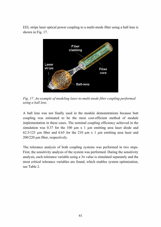
61
EEL stripe laser optical power coupling to a multi-mode fiber using a ball lens is shown in Fig. 17.
Fig. 17. An example of modeling laser-to-multi-mode fiber coupling performed using a ball lens.
A ball lens was not finally used in the module demonstrations because butt coupling was estimated to be the most cost-efficient method of module implementation in these cases. The nominal coupling efficiency achieved in the simulation was 0.37 for the 100 µm x 1 µm emitting area laser diode and 62.5/125 µm fiber and 0.65 for the 210 µm x 1 µm emitting area laser and 200/220 µm fiber, respectively.
The tolerance analysis of both coupling systems was performed in two steps. First, the sensitivity analysis of the system was performed. During the sensitivity analysis, each tolerance variable using a 3σ value is simulated separately and the most critical tolerance variables are found, which enables system optimization, see Table 2.
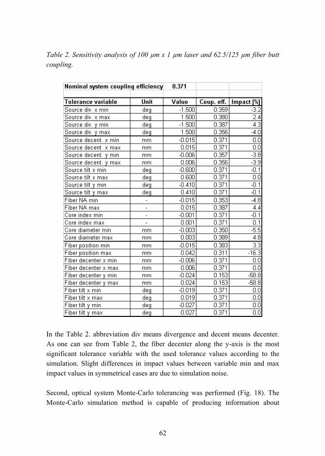
62
Table 2. Sensitivity analysis of 100 µm x 1 µm laser and 62.5/125 µm fiber butt coupling.
In the Table 2. abbreviation div means divergence and decent means decenter. As one can see from Table 2, the fiber decenter along the y-axis is the most significant tolerance variable with the used tolerance values according to the simulation. Slight differences in impact values between variable min and max impact values in symmetrical cases are due to simulation noise.
Second, optical system Monte-Carlo tolerancing was performed (Fig. 18). The Monte-Carlo simulation method is capable of producing information about
63
performance distribution of large manufacturing lot of modules. In Monte-Carlo tolerancing, all tolerance variables are simulated simultaneously as distributions and statistical information about the system performance is obtained. Typically, symmetrical distributions used in the Monte-Carlo simulations are Gaussian and non-symmetrical distributions are truncated Gaussian.
Fig. 18. Relative coupled power of 100 µm x 1 µm laser to 62.5/125 µm fiber.
As one can see from Fig. 18, the coupling efficiency peaks at around 0.36 and the maximum value is about 0.4.
4.3.3 Thermal management of high power laser diode
The thermal conductivity of LTCC material is quite low, about 3 W/m×K. However, the thermal conductivity of LTCC can be increased locally by processing heat spreaders, thermal vias and cooling channels on the LTCC substrate. This enables the use of LTCC substrate with a high-power laser diode. We developed a buried liquid cooling channel at the LTCC substrate underneath a laser diode. The biggest challenge was to develop the manufacturing methods for a buried channel without excessive deformation of the substrate surface, which would deteriorate the passive alignment accuracy and fiber-to-laser coupling efficiency. The channel structure, 1.65 mm wide and with a total length of about 30 mm, was punched on two tape layers that were buried two layers
64
deep. To prevent sagging of the LTCC stack during the lamination, the buried channel was filled with an organic precision machined filler insert, which burns off efficiently during the co-firing. The final dimensions of the channel cross section were 1.4 mm x 0.4 mm. The planarity of the surface on top of the buried channel was measured on eight samples, showing a typical warpage of 2 5 µm, and 7 µm in the worst case. In the module packaging process the warping effect is added to the laser diode height tolerance chain. Obviously, to introduce a minimum amount of warping the thickness of the organic insert must be controlled very accurately. The implemented cooling channel cross section is shown in Fig. 19.
Fig. 19. Cooling channel cross section 1.4 mm x 0.4 mm.
4.3.4 Packaging of the modules
In order to test the achievable laser-to-fiber passive alignment accuracy, a series containing 40 modules in two different series was realized using a six layer LTCC substrate, with a size of 22 mm x 25 mm. To test the hermeticity of the laser modules, a series containing eight modules was realized utilizing LTCC substrate, with a size of 10 mm x 22 mm.
In the alignment accuracy series the packaging started with laser chip alignment and attachment to the LTCC substrate gold metallization. The laser chip dimensions were 117 µm (H) x 200 µm (W) x 1000 µm (L). The laser chip was aligned with a flip-chip bonder and attached to the LTCC substrate by a
65
50%In/50%Pb solder perform. The solder perform size was 200 µm x 200 µm and thickness of 20 µm was used in the attachment. The upper contact was wire-bonded by a wedge-bonder using a 25 µm diameter gold wire.
A 62.5/125 µm multi-mode graded-index NA = 0.275 fiber (Spectran) was aligned manually to the LTCC groove under a microscope. The separation between the laser and the fiber was adjusted to about 40 um. The fiber was pressed to the groove using a small weight at the fiber center and epoxy bonded using three separate drops of Loctite 3525 UV-epoxy. The strain relief was realized by bonding the fiber buffer to the widened groove using the same epoxy. In Fig. 20 a passively aligned fiber pigtailed laser module is shown.
Fig. 20. Passively aligned fiber pigtailed laser module.
In the hermetic module series the used laser chip dimensions were 115 µm (H) x 500 µm (W) x 1000 µm (L) and the fiber was 200/220 µm. In addition, the module structure contained also a frame and a lid. The frame material was Kovar and it was tooled by 5-axis machine tooling. Before soldering the frame was electro-galvanized with nickel. Sn62Pb36Ag2 solder paste was dispensed around the frame and the frame was aligned with the substrate and then soldered. Solder was melted using an integrated thermal resistor formed by the metallization on the LTCC substrate.
66
The hermetic fiber feed-through was processed into the frame using a glass preform (DIEMAT DM2700PF). DM2700PF is a low-temperature glass preform designed specifically for hermetic optical fiber sealing. The glass has the following key properties: coefficient of thermal expansion 7.5 ppm/°C, glass transition temperature 215°C, density 4.5 g/cm3 and sealing temperature 320350 °C. The glass preform was heated by a hot gas to the melting temperature of the preform, which in turn collapsed around the fiber and wetted down the inside diameter of the ferrule. After the fiber sealing, the metallic strain relief tube and heat-shrinkable plastic creating the mechanical shields were assembled over the junction area with a UV-epoxy. The module was dried at 80°C for 24 hours before the sealing. Finally, a Kovar lid was attached to the top of the frame by laser welding in inert gas. The dimensions of the module are 22 mm (L) x 10 mm (W) x 4 mm (H). In Fig. 21, the manufactured module and the LTCC platform are shown.
Fig. 21. Hermetic fiber pigtailed laser module and LTCC platform.
4.3.5 Characterizations of the modules
The accuracy of laser diode-to-fiber passive alignment on the LTCC substrate was characterized by measuring alignment errors of assembled devices from the

67
realized modules. Wyko NT 3300 white light interferometer and Smartscope 200 optical 3D coordinate measurement system were used in the measurements. Table 3 shows the measured alignment tolerances.
Table 3. Measured alignment tolerances.
The transverse alignment errors in both series are under 9.1 µm, which suggests good coupling efficiency between laser diode and fiber.
The coupling efficiency of the modules was measured so that the fiber coupled power was first measured after module assembly by an optical power meter applying a 10 mm square silicon detector. Second, the substrate was cut near the laser diode and the total emitted power produced by the laser diode was measured using the same meter and detector. The coupling efficiency was achieved by simply dividing the fiber-coupled power by the total power. The average coupling efficiency and distribution are shown in Table 4.
Table 4. Measured average coupling efficiency and distribution in prototype series.
The total number of operational modules was 13 in the AT series and 16 in the A2 series. The total number of manufactured modules was 40. A pre-study found poor laser output with 11 modules, and fibers were not assembled on those modules.
68
As one can see from Table 4, the average coupling efficiency in the A2 series is better than in the AT series. This is very consistent with the fact that the measured alignment errors are smaller in the A2 series than in the AT series. The distribution of coupling efficiency in both series is wider than expected based on the simulations. Laser near- and far-field intensity distributions were measured in order to see the accuracy of the laser model used. Near-field intensity distribution was measured by imaging a laser facet to a CCD camera detector using a microscope objective. In Fig. 22, an example of the measured spatial intensity distribution is shown.
Fig. 22. Example of measured laser spatial near-field intensity.
We can see from Fig. 22 that the laser near-field irradiance distribution is clearly a multimode and not a top hat as used in the initial simulations. There is an intensity drop in the middle of the laser facet facing the fiber core in butt coupling at nominal alignment. This causes a clear reduction in the coupling efficiency. In the opposite case with a very bright laser center area, the coupling efficiency would be higher than nominally possible with a top hat spatial irradiance laser model. Therefore, a more accurate laser model is needed in order to achieve truly predictive simulations. Finally, characterized and qualified devices are needed for high-yield passive packaging production.
69
Cooling system efficiency was tested by running a high-power laser diode with and without water-cooling and by measuring surface temperature near the laser diode using a thermistor. However, the thermistor measurement does not measure the laser surface temperature. In order to get a better view of laser surface temperature, a thermal camera model SC3000 manufactured by FLIR Systems was used. The ambient temperature was 24°C, cooling water temperature 22.5°C and flow rate 50 ml/min during the measurements. Simulated (Flotherm) and measured temperature distributions are shown in Fig. 23.
Fig. 23. Simulated (left) and measured (right) laser surface temperatures.
As one can see from Fig. 23, a fairly good correspondence between the simulated and measured temperature values was achieved. The temperature maximum value in the simulation was achieved at the laser active layer near the front mirror surface.
The dimensions of the implemented hermetic module were 22 mm (L) x 10 mm (W) x 4 mm (H), so the total volume of the package was 0.88 cm3. The maximum allowed leak rate of 1 x 10⁻⁷ atm × cm3/s under 1 cm3 volume module was specified in the applied MIL-STD-883F method 1014.9 specification. A leak rate of 1 × 10⁻⁷ 8 x 10⁻⁷ atm × cm3/s was measured in the helium leak tests of the final operational prototypes with a fine leak tester, model. The leak rate for the dummy modules using a buffer stripped fiber without a rubber guard tube was 3 × 10⁻⁹ 1 x 10⁻⁸ atm × cm3/s. The measured leak rates proved that the developed packaging was hermetic. The clearly higher leak rate in the final
70
module leak measurement is mainly due to helium absorbed by the fiber polymer buffer layer and rubber guard tube in the pressurization process (Newman, 2001).
4.3.6 Evaluation of the passive alignment laser modules based on LTCC technology
The implementation of the passive alignment laser modules proved that it is possible to tool alignment structures such as grooves, holes and cavities to the LTCC substrates which enable passive alignment of a laser diode and a fiber with 3 5 µm transverse tolerances. The achieved transverse tolerance values are adequate for multimode applications, but inadequate for single mode applications.
When the laser diode chip and component tolerances are tight enough, the passive alignment allows high coupling efficiency realizations of multimode fiber pigtailed laser modules. The multimode fiber pigtailed laser modules can be used in optical interconnection and sensor systems. Due to the limited bandwidth of multimode optical interconnection system, the number of potential applications, however, is quite limited. Sensor applications requiring high transmitter power are one potential application for the developed technology due to the fact that the high-power lasers used in these applications are mainly multimode lasers.
The LTCC substrate was possible to equip with cooling structures to enable thermal management of high-power devices. The demonstrated structures include buried cooling channel, thermal vias and heat spreaders. The utilization of buried cooling channel and thermal vias clearly decreased the temperature of high-power laser diode. The low operational temperature of a high-power laser diode is important in order to achieve a long lifetime for the device.
LTCC substrate is inherently hermetic and it was used as an integral part of passively aligned laser module packaging. The implemented laser modules were hermetic according to the performed leak tests. The demonstrated packaging has good potential to enable hermetic packaging of fiber pigtailed laser modules cost-efficiently.
71
4.4 In-mold integration of VCSEL collimator
VCSEL collimator integration in injection molding process was studied in this work (Paper V).
4.4.1 Manufacturing concept
The in-mould integration concept for photonic module manufacturing is as follows. Electronic substrates such as FR4 or LTCC substrates are processed and active devices, semiconductor chips, are assembled on the substrates. The manufactured sub-modules are used as inserts in the injection molding process, in which the module optical and mechanical interconnections are implemented (Paper V). The sealing of the active devices and refractive index matching between chip semiconductor material and air is achieved at the same time.
The main features of the manufacturing concept are the utilization of bare semiconductor chips assembled on the electronic substrates and the use of these electronic sub-modules as inserts in injection molding and integration with optics and mechanics in an injection molding process.
4.4.2 Design of the demonstrator module
The VCSEL module was planned to be used as an illuminator module in a compact hologram reader system. The optical design of the lens was based on the device selection for the application. A red VCSEL device seemed to be a good choice for the application due to its vertical beam radiation and visibility to the user. The possibility to use the system as a replacement system for a pointer laser system based on an edge-emitting laser seemed to be very attractive as well. The selected VCSEL device measures were 270 µm x 200 µm x 170 µm (LxWxH) and its active area diameter was 10 µm, beam divergence 13 deg (FWHM) and emission peak wavelength of 664.5 nm.
In the optical system design performed using OSLO, the target values for illumination beam were as following. The beam 1/e2 diameter in the exit pupil should be 1.5 mm and the maximum illumination beam divergence 2 mrad. The
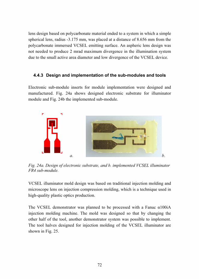
72
lens design based on polycarbonate material ended to a system in which a simple spherical lens, radius -3.175 mm, was placed at a distance of 8.656 mm from the polycarbonate immersed VCSEL emitting surface. An aspheric lens design was not needed to produce 2 mrad maximum divergence in the illumination system due to the small active area diameter and low divergence of the VCSEL device.
4.4.3 Design and implementation of the sub-modules and tools
Electronic sub-module inserts for module implementation were designed and manufactured. Fig. 24a shows designed electronic substrate for illuminator module and Fig. 24b the implemented sub-module.
a. b.
Fig. 24a. Design of electronic substrate, and b. implemented VCSEL illuminator FR4 sub-module.
VCSEL illuminator mold design was based on traditional injection molding and microscope lens on injection compression molding, which is a technique used in high-quality plastic optics production.
The VCSEL demonstrator was planned to be processed with a Fanuc α100iA injection molding machine. The mold was designed so that by changing the other half of the tool, another demonstrator system was possible to implement. The tool halves designed for injection molding of the VCSEL illuminator are shown in Fig. 25.
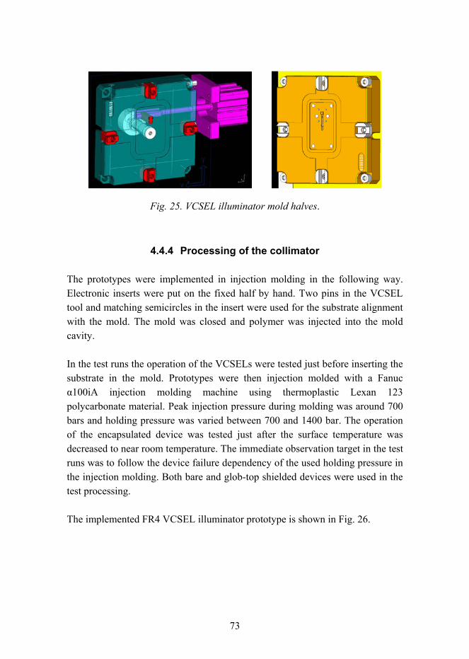
73
Fig. 25. VCSEL illuminator mold halves.
4.4.4 Processing of the collimator
The prototypes were implemented in injection molding in the following way. Electronic inserts were put on the fixed half by hand. Two pins in the VCSEL tool and matching semicircles in the insert were used for the substrate alignment with the mold. The mold was closed and polymer was injected into the mold cavity.
In the test runs the operation of the VCSELs were tested just before inserting the substrate in the mold. Prototypes were then injection molded with a Fanuc α100iA injection molding machine using thermoplastic Lexan 123 polycarbonate material. Peak injection pressure during molding was around 700 bars and holding pressure was varied between 700 and 1400 bar. The operation of the encapsulated device was tested just after the surface temperature was decreased to near room temperature. The immediate observation target in the test runs was to follow the device failure dependency of the used holding pressure in the injection molding. Both bare and glob-top shielded devices were used in the test processing.
The implemented FR4 VCSEL illuminator prototype is shown in Fig. 26.
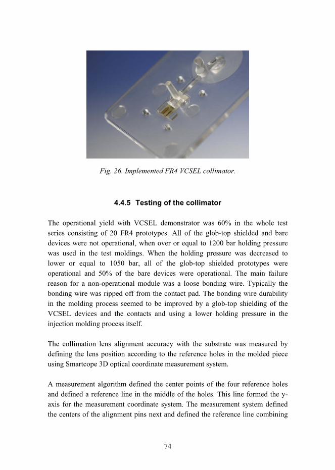
74
Fig. 26. Implemented FR4 VCSEL collimator.
4.4.5 Testing of the collimator
The operational yield with VCSEL demonstrator was 60% in the whole test series consisting of 20 FR4 prototypes. All of the glob-top shielded and bare devices were not operational, when over or equal to 1200 bar holding pressure was used in the test moldings. When the holding pressure was decreased to lower or equal to 1050 bar, all of the glob-top shielded prototypes were operational and 50% of the bare devices were operational. The main failure reason for a non-operational module was a loose bonding wire. Typically the bonding wire was ripped off from the contact pad. The bonding wire durability in the molding process seemed to be improved by a glob-top shielding of the VCSEL devices and the contacts and using a lower holding pressure in the injection molding process itself.
The collimation lens alignment accuracy with the substrate was measured by defining the lens position according to the reference holes in the molded piece using Smartcope 3D optical coordinate measurement system.
A measurement algorithm defined the center points of the four reference holes and defined a reference line in the middle of the holes. This line formed the y-axis for the measurement coordinate system. The measurement system defined the centers of the alignment pins next and defined the reference line combining
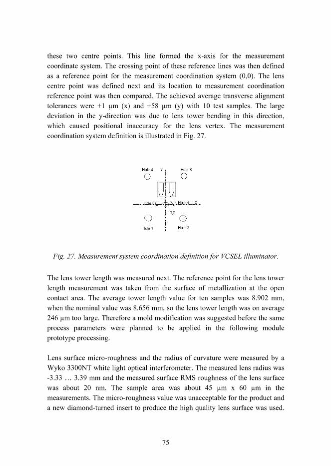
75
these two centre points. This line formed the x-axis for the measurement coordinate system. The crossing point of these reference lines was then defined as a reference point for the measurement coordination system (0,0). The lens centre point was defined next and its location to measurement coordination reference point was then compared. The achieved average transverse alignment tolerances were +1 µm (x) and +58 µm (y) with 10 test samples. The large deviation in the y-direction was due to lens tower bending in this direction, which caused positional inaccuracy for the lens vertex. The measurement coordination system definition is illustrated in Fig. 27.
Fig. 27. Measurement system coordination definition for VCSEL illuminator.
The lens tower length was measured next. The reference point for the lens tower length measurement was taken from the surface of metallization at the open contact area. The average tower length value for ten samples was 8.902 mm, when the nominal value was 8.656 mm, so the lens tower length was on average 246 µm too large. Therefore a mold modification was suggested before the same process parameters were planned to be applied in the following module prototype processing.
Lens surface micro-roughness and the radius of curvature were measured by a Wyko 3300NT white light optical interferometer. The measured lens radius was -3.33 3.39 mm and the measured surface RMS roughness of the lens surface was about 20 nm. The sample area was about 45 µm x 60 µm in the measurements. The micro-roughness value was unacceptable for the product and a new diamond-turned insert to produce the high quality lens surface was used.
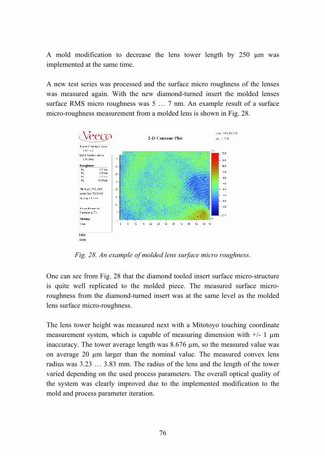
76
A mold modification to decrease the lens tower length by 250 µm was implemented at the same time.
A new test series was processed and the surface micro roughness of the lenses was measured again. With the new diamond-turned insert the molded lenses surface RMS micro roughness was 5 7 nm. An example result of a surface micro-roughness measurement from a molded lens is shown in Fig. 28.
Fig. 28. An example of molded lens surface micro roughness.
One can see from Fig. 28 that the diamond tooled insert surface micro-structure is quite well replicated to the molded piece. The measured surface micro-roughness from the diamond-turned insert was at the same level as the molded lens surface micro-roughness.
The lens tower height was measured next with a Mitotoyo touching coordinate measurement system, which is capable of measuring dimension with +/- 1 µm inaccuracy. The tower average length was 8.676 µm, so the measured value was on average 20 µm larger than the nominal value. The measured convex lens radius was 3.23 3.83 mm. The radius of the lens and the length of the tower varied depending on the used process parameters. The overall optical quality of the system was clearly improved due to the implemented modification to the mold and process parameter iteration.
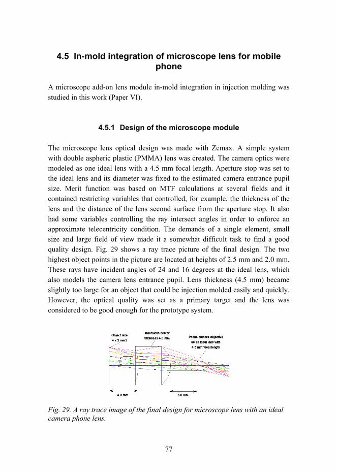
77
4.5 In-mold integration of microscope lens for mobile phone
A microscope add-on lens module in-mold integration in injection molding was studied in this work (Paper VI).
4.5.1 Design of the microscope module
The microscope lens optical design was made with Zemax. A simple system with double aspheric plastic (PMMA) lens was created. The camera optics were modeled as one ideal lens with a 4.5 mm focal length. Aperture stop was set to the ideal lens and its diameter was fixed to the estimated camera entrance pupil size. Merit function was based on MTF calculations at several fields and it contained restricting variables that controlled, for example, the thickness of the lens and the distance of the lens second surface from the aperture stop. It also had some variables controlling the ray intersect angles in order to enforce an approximate telecentricity condition. The demands of a single element, small size and large field of view made it a somewhat difficult task to find a good quality design. Fig. 29 shows a ray trace picture of the final design. The two highest object points in the picture are located at heights of 2.5 mm and 2.0 mm. These rays have incident angles of 24 and 16 degrees at the ideal lens, which also models the camera lens entrance pupil. Lens thickness (4.5 mm) became slightly too large for an object that could be injection molded easily and quickly. However, the optical quality was set as a primary target and the lens was considered to be good enough for the prototype system.
Fig. 29. A ray trace image of the final design for microscope lens with an ideal camera phone lens.
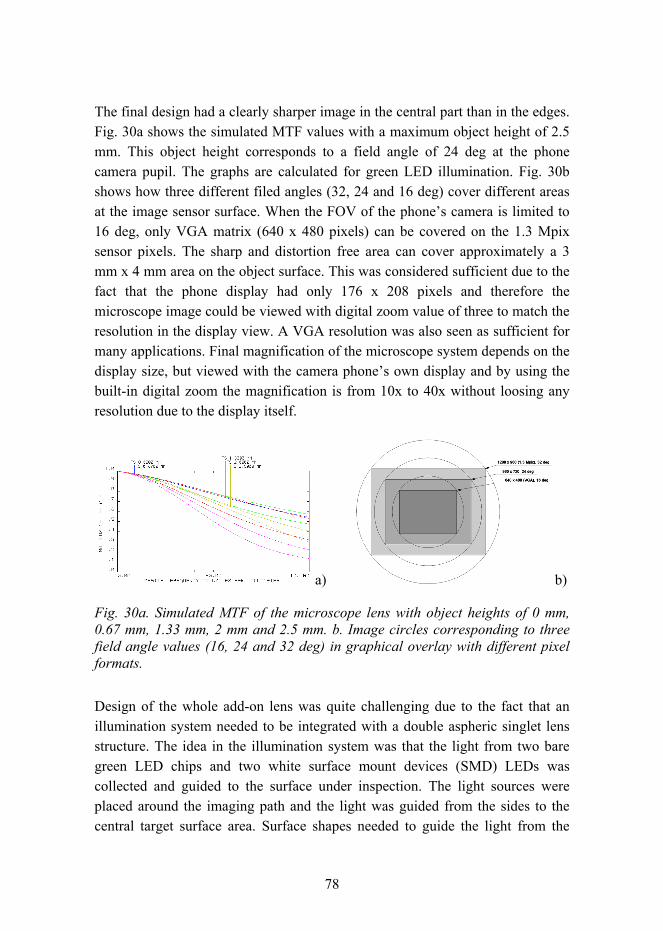
78
The final design had a clearly sharper image in the central part than in the edges. Fig. 30a shows the simulated MTF values with a maximum object height of 2.5 mm. This object height corresponds to a field angle of 24 deg at the phone camera pupil. The graphs are calculated for green LED illumination. Fig. 30b shows how three different filed angles (32, 24 and 16 deg) cover different areas at the image sensor surface. When the FOV of the phones camera is limited to 16 deg, only VGA matrix (640 x 480 pixels) can be covered on the 1.3 Mpix sensor pixels. The sharp and distortion free area can cover approximately a 3 mm x 4 mm area on the object surface. This was considered sufficient due to the fact that the phone display had only 176 x 208 pixels and therefore the microscope image could be viewed with digital zoom value of three to match the resolution in the display view. A VGA resolution was also seen as sufficient for many applications. Final magnification of the microscope system depends on the display size, but viewed with the camera phones own display and by using the built-in digital zoom the magnification is from 10x to 40x without loosing any resolution due to the display itself.
a) b)
Fig. 30a. Simulated MTF of the microscope lens with object heights of 0 mm, 0.67 mm, 1.33 mm, 2 mm and 2.5 mm. b. Image circles corresponding to three field angle values (16, 24 and 32 deg) in graphical overlay with different pixel formats.
Design of the whole add-on lens was quite challenging due to the fact that an illumination system needed to be integrated with a double aspheric singlet lens structure. The idea in the illumination system was that the light from two bare green LED chips and two white surface mount devices (SMD) LEDs was collected and guided to the surface under inspection. The light sources were placed around the imaging path and the light was guided from the sides to the central target surface area. Surface shapes needed to guide the light from the
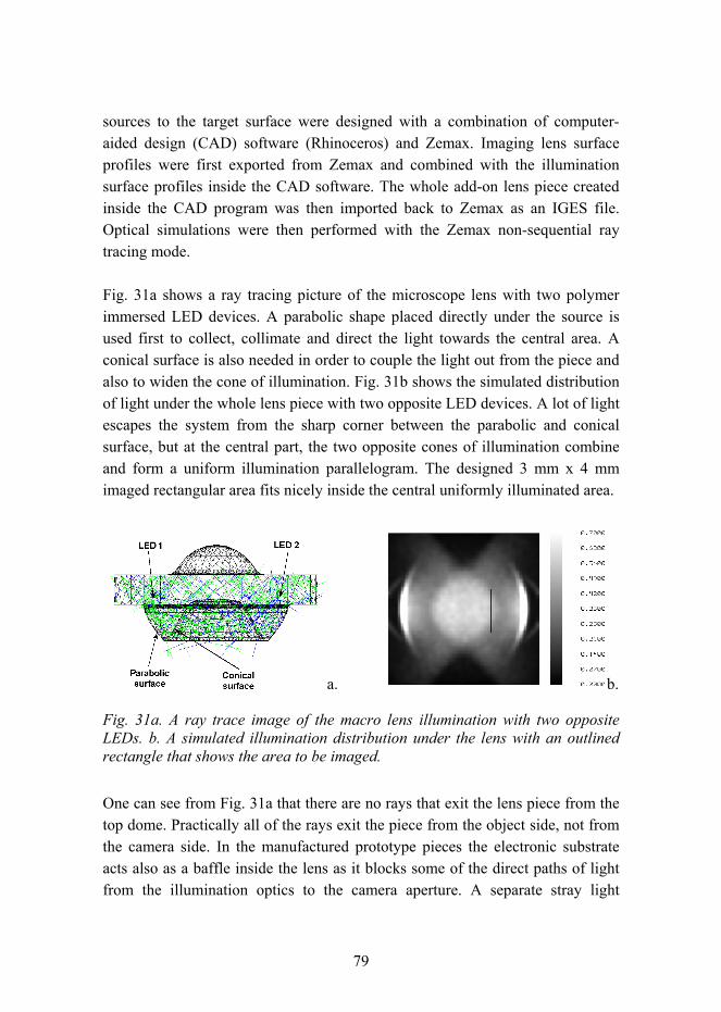
79
sources to the target surface were designed with a combination of computer-aided design (CAD) software (Rhinoceros) and Zemax. Imaging lens surface profiles were first exported from Zemax and combined with the illumination surface profiles inside the CAD software. The whole add-on lens piece created inside the CAD program was then imported back to Zemax as an IGES file. Optical simulations were then performed with the Zemax non-sequential ray tracing mode.
Fig. 31a shows a ray tracing picture of the microscope lens with two polymer immersed LED devices. A parabolic shape placed directly under the source is used first to collect, collimate and direct the light towards the central area. A conical surface is also needed in order to couple the light out from the piece and also to widen the cone of illumination. Fig. 31b shows the simulated distribution of light under the whole lens piece with two opposite LED devices. A lot of light escapes the system from the sharp corner between the parabolic and conical surface, but at the central part, the two opposite cones of illumination combine and form a uniform illumination parallelogram. The designed 3 mm x 4 mm imaged rectangular area fits nicely inside the central uniformly illuminated area.
a. b.
Fig. 31a. A ray trace image of the macro lens illumination with two opposite LEDs. b. A simulated illumination distribution under the lens with an outlined rectangle that shows the area to be imaged.
One can see from Fig. 31a that there are no rays that exit the lens piece from the top dome. Practically all of the rays exit the piece from the object side, not from the camera side. In the manufactured prototype pieces the electronic substrate acts also as a baffle inside the lens as it blocks some of the direct paths of light from the illumination optics to the camera aperture. A separate stray light
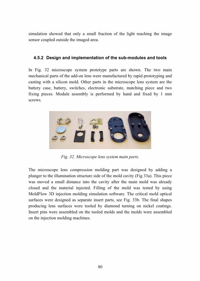
80
simulation showed that only a small fraction of the light reaching the image sensor coupled outside the imaged area.
4.5.2 Design and implementation of the sub-modules and tools
In Fig. 32 microscope system prototype parts are shown. The two main mechanical parts of the add-on lens were manufactured by rapid prototyping and casting with a silicon mold. Other parts in the microscope lens system are the battery case, battery, switches, electronic substrate, matching piece and two fixing pieces. Module assembly is performed by hand and fixed by 1 mm screws.
Fig. 32. Microscope lens system main parts.
The microscope lens compression molding part was designed by adding a plunger to the illumination structure side of the mold cavity (Fig 33a). This piece was moved a small distance into the cavity after the main mold was already closed and the material injected. Filling of the mold was tested by using MoldFlow 3D injection molding simulation software. The critical mold optical surfaces were designed as separate insert parts, see Fig. 33b. The final shapes producing lens surfaces were tooled by diamond turning on nickel coatings. Insert pins were assembled on the tooled molds and the molds were assembled on the injection molding machines.
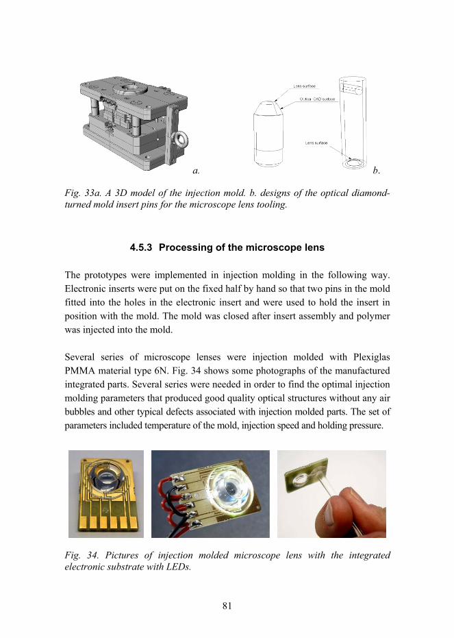
81
a. b.
Fig. 33a. A 3D model of the injection mold. b. designs of the optical diamond-turned mold insert pins for the microscope lens tooling.
4.5.3 Processing of the microscope lens
The prototypes were implemented in injection molding in the following way. Electronic inserts were put on the fixed half by hand so that two pins in the mold fitted into the holes in the electronic insert and were used to hold the insert in position with the mold. The mold was closed after insert assembly and polymer was injected into the mold.
Several series of microscope lenses were injection molded with Plexiglas PMMA material type 6N. Fig. 34 shows some photographs of the manufactured integrated parts. Several series were needed in order to find the optimal injection molding parameters that produced good quality optical structures without any air bubbles and other typical defects associated with injection molded parts. The set of parameters included temperature of the mold, injection speed and holding pressure.
Fig. 34. Pictures of injection molded microscope lens with the integrated electronic substrate with LEDs.
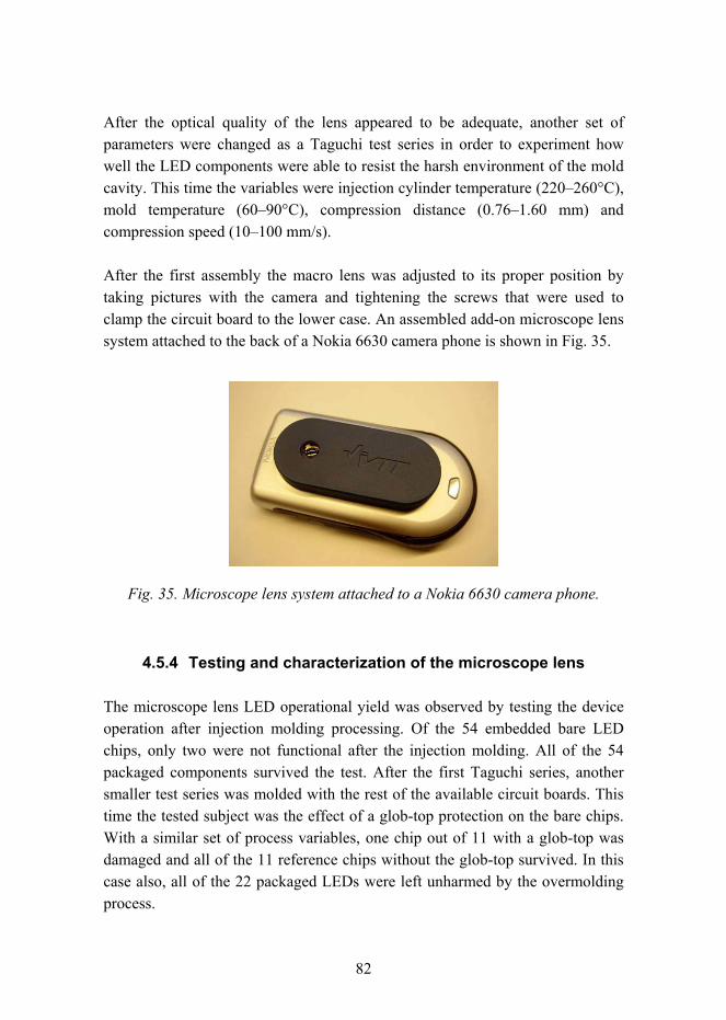
82
After the optical quality of the lens appeared to be adequate, another set of parameters were changed as a Taguchi test series in order to experiment how well the LED components were able to resist the harsh environment of the mold cavity. This time the variables were injection cylinder temperature (220260°C), mold temperature (6090°C), compression distance (0.761.60 mm) and compression speed (10100 mm/s).
After the first assembly the macro lens was adjusted to its proper position by taking pictures with the camera and tightening the screws that were used to clamp the circuit board to the lower case. An assembled add-on microscope lens system attached to the back of a Nokia 6630 camera phone is shown in Fig. 35.
Fig. 35. Microscope lens system attached to a Nokia 6630 camera phone.
4.5.4 Testing and characterization of the microscope lens
The microscope lens LED operational yield was observed by testing the device operation after injection molding processing. Of the 54 embedded bare LED chips, only two were not functional after the injection molding. All of the 54 packaged components survived the test. After the first Taguchi series, another smaller test series was molded with the rest of the available circuit boards. This time the tested subject was the effect of a glob-top protection on the bare chips. With a similar set of process variables, one chip out of 11 with a glob-top was damaged and all of the 11 reference chips without the glob-top survived. In this case also, all of the 22 packaged LEDs were left unharmed by the overmolding process.
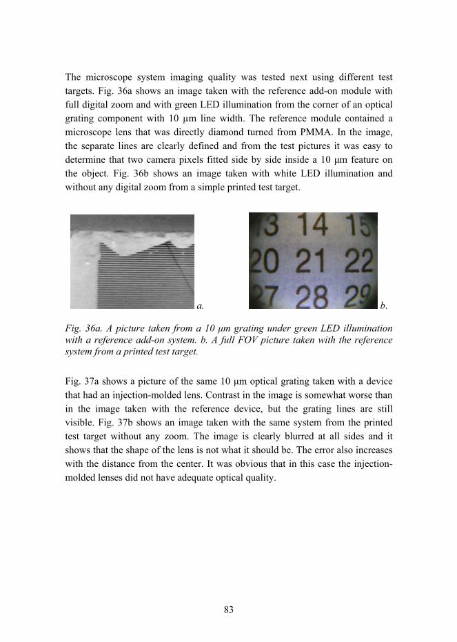
83
The microscope system imaging quality was tested next using different test targets. Fig. 36a shows an image taken with the reference add-on module with full digital zoom and with green LED illumination from the corner of an optical grating component with 10 µm line width. The reference module contained a microscope lens that was directly diamond turned from PMMA. In the image, the separate lines are clearly defined and from the test pictures it was easy to determine that two camera pixels fitted side by side inside a 10 µm feature on the object. Fig. 36b shows an image taken with white LED illumination and without any digital zoom from a simple printed test target.
a. b.
Fig. 36a. A picture taken from a 10 µm grating under green LED illumination with a reference add-on system. b. A full FOV picture taken with the reference system from a printed test target.
Fig. 37a shows a picture of the same 10 µm optical grating taken with a device that had an injection-molded lens. Contrast in the image is somewhat worse than in the image taken with the reference device, but the grating lines are still visible. Fig. 37b shows an image taken with the same system from the printed test target without any zoom. The image is clearly blurred at all sides and it shows that the shape of the lens is not what it should be. The error also increases with the distance from the center. It was obvious that in this case the injection-molded lenses did not have adequate optical quality.
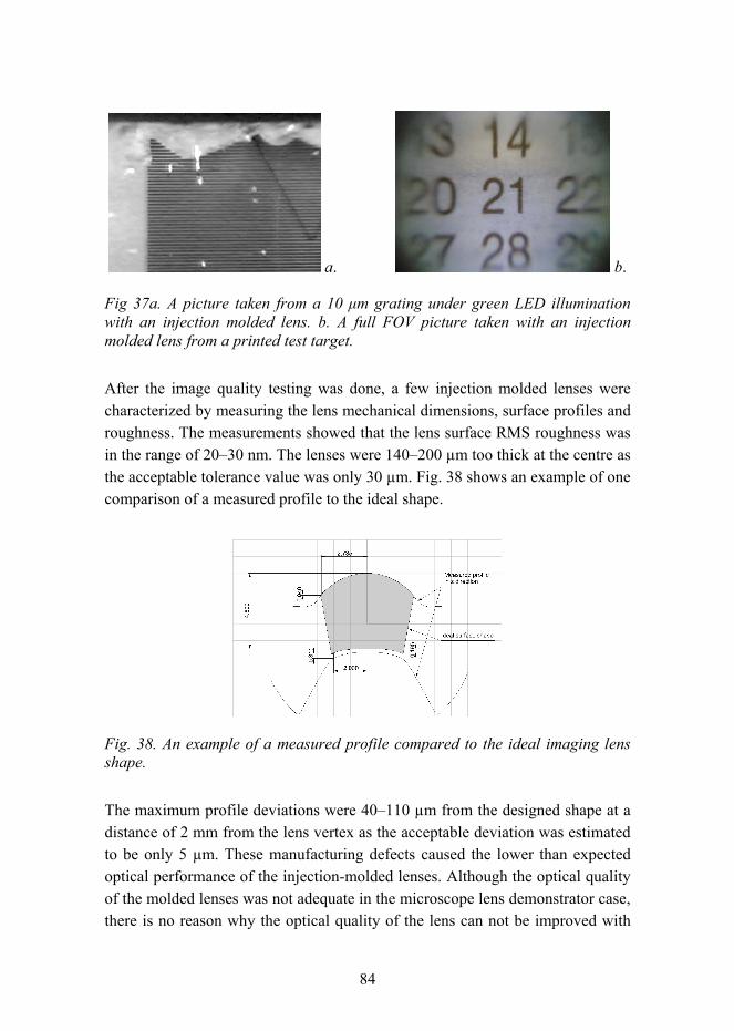
84
a. b.
Fig 37a. A picture taken from a 10 µm grating under green LED illumination with an injection molded lens. b. A full FOV picture taken with an injection molded lens from a printed test target.
After the image quality testing was done, a few injection molded lenses were characterized by measuring the lens mechanical dimensions, surface profiles and roughness. The measurements showed that the lens surface RMS roughness was in the range of 2030 nm. The lenses were 140200 µm too thick at the centre as the acceptable tolerance value was only 30 µm. Fig. 38 shows an example of one comparison of a measured profile to the ideal shape.
Fig. 38. An example of a measured profile compared to the ideal imaging lens shape.
The maximum profile deviations were 40110 µm from the designed shape at a distance of 2 mm from the lens vertex as the acceptable deviation was estimated to be only 5 µm. These manufacturing defects caused the lower than expected optical performance of the injection-molded lenses. Although the optical quality of the molded lenses was not adequate in the microscope lens demonstrator case, there is no reason why the optical quality of the lens can not be improved with
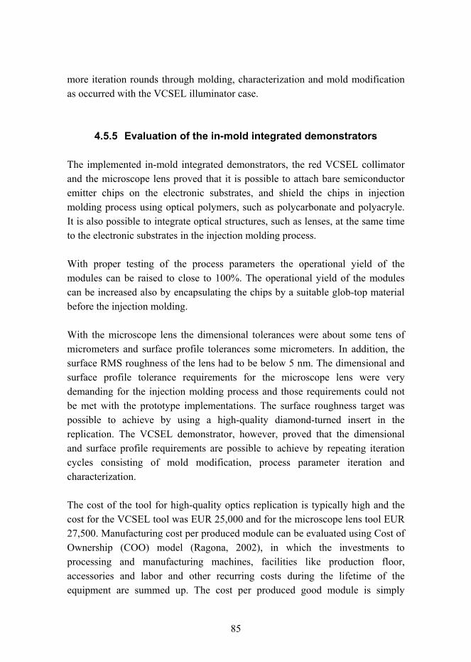
85
more iteration rounds through molding, characterization and mold modification as occurred with the VCSEL illuminator case.
4.5.5 Evaluation of the in-mold integrated demonstrators
The implemented in-mold integrated demonstrators, the red VCSEL collimator and the microscope lens proved that it is possible to attach bare semiconductor emitter chips on the electronic substrates, and shield the chips in injection molding process using optical polymers, such as polycarbonate and polyacryle. It is also possible to integrate optical structures, such as lenses, at the same time to the electronic substrates in the injection molding process.
With proper testing of the process parameters the operational yield of the modules can be raised to close to 100%. The operational yield of the modules can be increased also by encapsulating the chips by a suitable glob-top material before the injection molding.
With the microscope lens the dimensional tolerances were about some tens of micrometers and surface profile tolerances some micrometers. In addition, the surface RMS roughness of the lens had to be below 5 nm. The dimensional and surface profile tolerance requirements for the microscope lens were very demanding for the injection molding process and those requirements could not be met with the prototype implementations. The surface roughness target was possible to achieve by using a high-quality diamond-turned insert in the replication. The VCSEL demonstrator, however, proved that the dimensional and surface profile requirements are possible to achieve by repeating iteration cycles consisting of mold modification, process parameter iteration and characterization.
The cost of the tool for high-quality optics replication is typically high and the cost for the VCSEL tool was EUR 25,000 and for the microscope lens tool EUR 27,500. Manufacturing cost per produced module can be evaluated using Cost of Ownership (COO) model (Ragona, 2002), in which the investments to processing and manufacturing machines, facilities like production floor, accessories and labor and other recurring costs during the lifetime of the equipment are summed up. The cost per produced good module is simply
86
achieved by dividing all the manufacturing costs by a number of produced acceptable modules. Thus COO depends on the production rate, equipment acquisition cost, equipment reliability, maintenance, utilization, throughput, yield, rework and scrap cost and useful life time of the system.
The estimated COO of the VCSEL collimator was EUR 0.14, when 10 Million good modules were produced in a year. It is important to notice that the total costs of the module was evaluated to be EUR 0.84, so the packaging costs were about 20% and component costs about 80% of the module total costs. It seems to be a normal trend that the component cost portion about total cost increases and the packaging cost portion about total cost decreases, when the production lot size increases. Therefore, the component cost is very critical in the volume production.
The COO modeling can be correspondingly applied to estimate production cost of any photonic system, when accurate information about production yield and throughput rate is available. The achieved results with the demonstrators suggest that the in-mold integration can be considered a very cost-efficient method to produce intelligently integrated photonic products.

87
5. Discussion The most important general characteristics of a photonic module are performance, cost and reliability. The order of importance between these characteristics depends strongly on the application and in some applications the order of importance can even be cost, cost and cost.
The very essential issue in the photonic module packaging related to the performance is the optical coupling implementation. The efficient optical coupling between emitters and waveguides, the active area dimensions of which can be only some micrometers with single-mode devices requiring sub-micrometer alignment tolerances, is very challenging especially when the coupling has to be implemented with high cost-efficiency. In this thesis the cost-efficiency is applied through the integration in such a way that several functions are typically combined in a single piece. Implementation of passive alignment features on a multilayer ceramic electronic substrate, for example, combine electronic functions and optomechanical high accuracy features in a single platform enabling passive alignment of devices. The passive alignment of devices enable module implementation with lesser components, more economy assembly machines and shorter throughput time compared to the active alignment, if the component and substrate tolerances are tight enough. By means of passive alignment and integration, an improved cost-efficiency of the modules is possible to attain.
In this thesis the performance of the passive alignment substrates was seen to be adequate for multimode applications. Further studies are needed in order to achieve alignment tolerances required in single-mode applications. It seems that the use of new photoimageable materials offers the greatest opportunity for improvement of the alignment structure accuracy. Another benefit would be that the passive alignment structures or alignment fiducials for the photonic devices can be manufactured in the same process. Another possibility to reach accuracy for single-mode applications is to combine passive and active alignment by implementing the rough alignment passively and then applying the required fine-tuning by an additional actuator. In practice this can be implemented by a fine adjustment actuator integrated to the substrate. It is worth mentioning here that the high-accuracy silicon substrates are capable of providing required passive alignment accuracy for single-mode applications.
88
The experiences in the course of this thesis have shown that the possibility to evaluate packaging concepts and optimize detailed structures and tolerances through simulations offer a very effective tool for photonic module integration. The sensitivity analysis informs the most significant tolerance variables and directs the enhance effort to the most important variable targets where the largest benefit is gained. This is an important part in the cost-effective packaging design of modules. The sensitivity analysis can be supplemented by Monte-Carlo tolerancing in which all tolerance variables are simulated simultaneously as distributions and statistical information about the system performance is obtained. This kind of simulation information can be used to evaluate how much a certain tolerance value improvement is expected to increase the yield. Finally, cost-of-ownership modeling can be applied to estimate manufacturing cost of the packaged modules. The simulations are important tools, but in the end the implementation and characterization of the prototype devices and modules verifies designs and offers information to enhance design and simulation models.
The most important environmental factors that deteriorate photonic modules and shorten the lifetime of active devices are probably temperature and moisture. Therefore, the thermal management of high-power laser diodes and LEDs is very critical and electronic substrates have to be equipped with effective thermal vias, heat spreaders and possibly with cooling channels in order to enable reliable and stable operation of devices.
The effect of moisture can be revoked by sealing the sensitive devices hermetically. Hermetic sealing provides tight barrier also for water vapor and it enables long-term reliability for photonic devices. The created packaging concept utilizing ceramic substrates as an integral part of the hermetic package can be further utilized with various module implementations requiring hermetic sealing of devices.
Epoxy or polymer encapsulation revokes water penetration and retards water vapor penetration, but finally water vapor reaches the semiconductor surface and bonding wire joint and the deterioration of the junction and joint accelerates rapidly. The long-term operational reliability of the in-mold integrated modules has not yet been studied very well. Performed tests so far showed that the operational temperature of devices is a very critical issue, when considering in-mold integrated module lifetime. In practice, the excess thermal power has to be
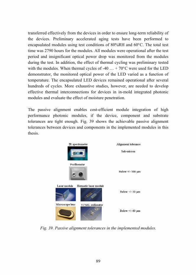
89
transferred effectively from the devices in order to ensure long-term reliability of the devices. Preliminary accelerated aging tests have been performed to encapsulated modules using test conditions of 80%RH and 60°C. The total test time was 2790 hours for the modules. All modules were operational after the test period and insignificant optical power drop was monitored from the modules during the test. In addition, the effect of thermal cycling was preliminary tested with the modules. When thermal cycles of -40 + 70°C were used for the LED demonstrator, the monitored optical power of the LED varied as a function of temperature. The encapsulated LED devices remained operational after several hundreds of cycles. More exhaustive studies, however, are needed to develop effective thermal interconnections for devices in in-mold integrated photonic modules and evaluate the effect of moisture penetration.
The passive alignment enables cost-efficient module integration of high performance photonic modules, if the device, component and substrate tolerances are tight enough. Fig. 39 shows the achievable passive alignment tolerances between devices and components in the implemented modules in this thesis.
Fig. 39. Passive alignment tolerances in the implemented modules.
90
The IR spectrometer can be considered to present an example of the achievable integration level of MOEMS using silicon processing. Silicon processing enables sub-micron alignment tolerances between devices in monolithically integrated module. Infrared spectrometer implementation in this thesis proved that monolithic integration of high-speed optical functions and driving and signal processing electronics on a single silicon chip is technologically very demanding task and it was not feasible in this case.
The development work towards high performance and cost-effective monolithic PICs based on InP and GaAs materials for communication systems will continue in the future. The silicon technology development will also continue towards monolithic PIC, but the probability to reach the target is very low in the near future.
Most of the presented demonstrators are located within the hybrid integration theme. Hybrid integration enables effective combination of the high efficiency photonic sources produced by compound semiconductor technologies with photonic sensors and driving and processing electronics produced by silicon technologies.
There are no examples of heterogeneous integration presented in this thesis. The microscope lens and VCSEL collimator demonstrators, however, show one possible development direction to approach the heterogeneous integration theme. The plastics integration technology based on utilization of printed electronics substrates containing photonic devices combined with plastic optics using molding technologies seems to provide an example of a possible heterogeneous integration technology for photonic modules of the future. It could also be possible that processing and material technology development enables wafer bonding of polymer and thin silicon substrates and integration of optical components in a molding process in the future.
91
6. Summary In this thesis, we have developed ways to implement the very critical optical coupling between devices in photonic module packaging using passive alignment.
Silicon surface micromachining allows implementation of optical structures of devices and alignment between devices with sub-micron accuracy. The achieved high alignment and structural accuracy of devices in silicon processing is based on utilization of lithographic processes, which are well capable to produce below 100 nm features accurately. In this thesis a high integration level infrared spectrometer sensor module was demonstrated using silicon surface micromachining. It was noticed that silicon technology was capable to produce monolithically integrated emitter and detector on a silicon chip. The silicon technology, however, was not capable of producing dispersive optical component, driving and data processing electronics to a same chip and development of effective hybrid integration technologies is therefore still required.
As an example of utilizing electronic substrate in the photonic module hybrid integration, multilayer ceramics substrate technology was studied. A miniature profilometer based on an active triangular distance measurement principle was implemented on a multilayer ceramic substrate. The passively achieved transverse alignment accuracy in assembly between components was below +/- 100 µm, which was adequate to enable accurate measurements with the sensor system.
It is also possible to produce photonic modules using hybrid integration in which the alignment and optical coupling between devices and components is based on use of a suitable substrate with alignment structures or other mechanical alignment structure. In multimode fiber optics applications below +/- 5 µm and in single mode applications sub-micron alignment tolerances are typically required. The utilization of passive alignment in photonic is cost-efficient method to implement modules, when the tolerances of the devices and substrates are tight enough. In this thesis transverse alignment accuracy of 3 10 µm between laser diode and fiber was achieved using passive alignment based on multilayer ceramic substrate technology. The achieved passive alignment
92
accuracy is adequate for multimode applications, but inadequate for single mode applications.
The multilayer ceramic substrate was used as an integrated part of the casing structure in a passively packaged hermetic laser module demonstrator. The dimensions of the module were 22 mm (L) x 10 mm (W) x 4 mm (H) so the total volume of the package was 0.88 cm3. The maximum allowed leak rate of 1 x 10⁻⁷ atm × cm3/s under a 1 cm3 volume module was specified in the applied MIL standard for a hermetic module. A leak rate of 1 × 10⁻⁷ 8 x 10⁻⁷ atm × cm3/s was measured in the helium leak tests of the final operational prototypes. The leak rate for the dummy modules using a buffer stripped fiber without a rubber guard tube was 3 × 10⁻⁹ 1 x 10⁻⁸ atm × cm3/s. The measured leak rates proved that the developed packaging was hermetic.
The utilization of bare chips assembled on the substrates and encapsulated with polymer in the in-mold integration process was demonstrated successfully by a novel VCSEL illuminator for a future hologram reader and a microscope add-on lens for a Nokia 6630 mobile phone. Demonstrator modules were processed by encapsulating the bare emitter chips on FR4 substrates in optical polymer and processing the lens surfaces at the same time in injection molding process. Lens surface was molded on top of a source below +/- 60 µm transverse alignment tolerances, which was at adequate level in both demonstrators and also in many other sensor and illumination module applications. The required surface roughness of around 5 nm for replicated optical surfaces was possible to achieve using diamond tooled inserts. It was noticed that the high profile and dimensional accuracy requirements for imaging lenses can be obtained through mold modifications and process parameter iterations for the final production.
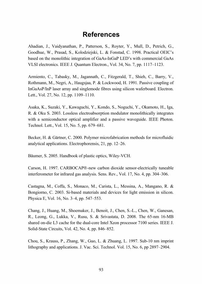
93
References Ahadian, J., Vaidyanathan, P., Patterson, S., Royter, Y., Mull, D., Petrich, G., Goodhue, W., Prasad, S., Kolodziejski, L. & Fonstad, C. 1998. Practical OEICs based on the monolithic integration of GaAs-InGaP LEDs with commercial GaAs VLSI electronics. IEEE J. Quantum Electron., Vol. 34, No. 7, pp. 11171123.
Armiento, C., Tabasky, M., Jagannath, C., Fitzgerald, T., Shieh, C., Barry, V., Rothmann, M., Negri, A., Haugsjaa, P. & Lockwood, H. 1991. Passive coupling of InGaAsP/InP laser array and singlemode fibres using silicon waferboard. Electron. Lett., Vol. 27, No. 12, pp. 11091110.
Asaka, K., Suzaki, Y., Kawaguchi, Y., Kondo, S., Noguchi, Y., Okamoto, H., Iga, R. & Oku S. 2003. Lossless electroabsorption modulator monolithically integrates with a semiconductor optical amplifier and a passive waveguide. IEEE Photon. Technol. Lett., Vol. 15, No. 5, pp. 679681.
Becker, H. & Gärtner, C. 2000. Polymer microfabrication methods for microfluidic analytical applications. Electrophorensis, 21, pp. 1226.
Bäumer, S. 2005. Handbook of plastic optics, Wiley-VCH.
Carson, H. 1997. CARBOCAP®-new carbon dioxide sensor-electrically tuneable interferometer for infrared gas analysis. Sens. Rev., Vol. 17, No. 4, pp. 304306.
Castagna, M., Coffa, S., Monaco, M., Carista, L., Messina, A., Mangano, R. & Bongiorno, C. 2003. Si-based materials and devices for light emission in silicon. Physica E, Vol. 16, No. 34, pp. 547553.
Chang, J., Huang, M., Shoemaker, J., Benoit, J., Chen, S.-L., Chen, W., Ganesan, R., Leong, G., Lukka, V., Rusu, S. & Srivastata, D. 2008. The 65-nm 16-MB shared on-die L3 cache for the dual-core Intel Xeon processor 7100 series. IEEE J. Solid-State Circuits, Vol. 42, No. 4, pp. 846852.
Chou, S., Krauss, P., Zhang, W., Guo, L. & Zhuang, L. 1997. Sub-10 nm imprint lithography and applications. J. Vac. Sci. Technol. Vol. 15, No. 6, pp 28972904.
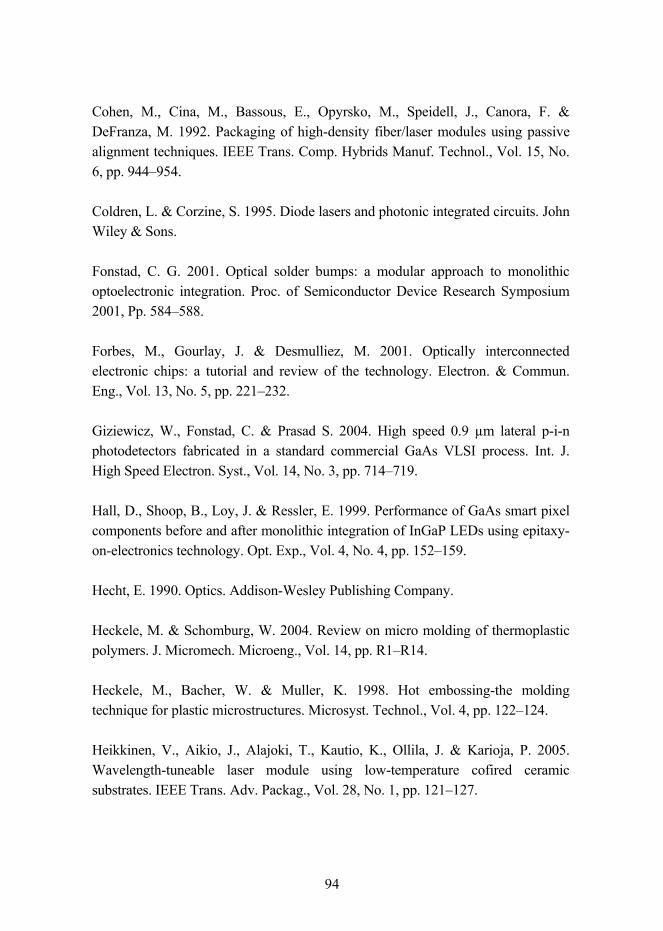
94
Cohen, M., Cina, M., Bassous, E., Opyrsko, M., Speidell, J., Canora, F. & DeFranza, M. 1992. Packaging of high-density fiber/laser modules using passive alignment techniques. IEEE Trans. Comp. Hybrids Manuf. Technol., Vol. 15, No. 6, pp. 944954.
Coldren, L. & Corzine, S. 1995. Diode lasers and photonic integrated circuits. John Wiley & Sons.
Fonstad, C. G. 2001. Optical solder bumps: a modular approach to monolithic optoelectronic integration. Proc. of Semiconductor Device Research Symposium 2001, Pp. 584588.
Forbes, M., Gourlay, J. & Desmulliez, M. 2001. Optically interconnected electronic chips: a tutorial and review of the technology. Electron. & Commun. Eng., Vol. 13, No. 5, pp. 221232.
Giziewicz, W., Fonstad, C. & Prasad S. 2004. High speed 0.9 µm lateral p-i-n photodetectors fabricated in a standard commercial GaAs VLSI process. Int. J. High Speed Electron. Syst., Vol. 14, No. 3, pp. 714719.
Hall, D., Shoop, B., Loy, J. & Ressler, E. 1999. Performance of GaAs smart pixel components before and after monolithic integration of InGaP LEDs using epitaxy-on-electronics technology. Opt. Exp., Vol. 4, No. 4, pp. 152159.
Hecht, E. 1990. Optics. Addison-Wesley Publishing Company.
Heckele, M. & Schomburg, W. 2004. Review on micro molding of thermoplastic polymers. J. Micromech. Microeng., Vol. 14, pp. R1R14.
Heckele, M., Bacher, W. & Muller, K. 1998. Hot embossing-the molding technique for plastic microstructures. Microsyst. Technol., Vol. 4, pp. 122124.
Heikkinen, V., Aikio, J., Alajoki, T., Kautio, K., Ollila, J. & Karioja, P. 2005. Wavelength-tuneable laser module using low-temperature cofired ceramic substrates. IEEE Trans. Adv. Packag., Vol. 28, No. 1, pp. 121127.
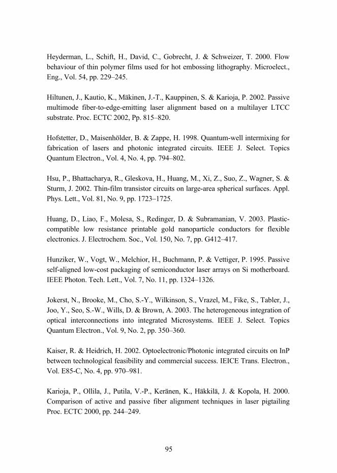
95
Heyderman, L., Schift, H., David, C., Gobrecht, J. & Schweizer, T. 2000. Flow behaviour of thin polymer films used for hot embossing lithography. Microelect., Eng., Vol. 54, pp. 229245.
Hiltunen, J., Kautio, K., Mäkinen, J.-T., Kauppinen, S. & Karioja, P. 2002. Passive multimode fiber-to-edge-emitting laser alignment based on a multilayer LTCC substrate. Proc. ECTC 2002, Pp. 815820.
Hofstetter, D., Maisenhölder, B. & Zappe, H. 1998. Quantum-well intermixing for fabrication of lasers and photonic integrated circuits. IEEE J. Select. Topics Quantum Electron., Vol. 4, No. 4, pp. 794802.
Hsu, P., Bhattacharya, R., Gleskova, H., Huang, M., Xi, Z., Suo, Z., Wagner, S. & Sturm, J. 2002. Thin-film transistor circuits on large-area spherical surfaces. Appl. Phys. Lett., Vol. 81, No. 9, pp. 17231725.
Huang, D., Liao, F., Molesa, S., Redinger, D. & Subramanian, V. 2003. Plastic-compatible low resistance printable gold nanoparticle conductors for flexible electronics. J. Electrochem. Soc., Vol. 150, No. 7, pp. G412417.
Hunziker, W., Vogt, W., Melchior, H., Buchmann, P. & Vettiger, P. 1995. Passive self-aligned low-cost packaging of semiconductor laser arrays on Si motherboard. IEEE Photon. Tech. Lett., Vol. 7, No. 11, pp. 13241326.
Jokerst, N., Brooke, M., Cho, S.-Y., Wilkinson, S., Vrazel, M., Fike, S., Tabler, J., Joo, Y., Seo, S.-W., Wills, D. & Brown, A. 2003. The heterogeneous integration of optical interconnections into integrated Microsystems. IEEE J. Select. Topics Quantum Electron., Vol. 9, No. 2, pp. 350360.
Kaiser, R. & Heidrich, H. 2002. Optoelectronic/Photonic integrated circuits on InP between technological feasibility and commercial success. IEICE Trans. Electron., Vol. E85-C, No. 4, pp. 970981.
Karioja, P., Ollila, J., Putila, V.-P., Keränen, K., Häkkilä, J. & Kopola, H. 2000. Comparison of active and passive fiber alignment techniques in laser pigtailing Proc. ECTC 2000, pp. 244249.
96
Karow, H. 2004. Fabrication methods for precision optics. John Wiley & Sons.
Koch, T. & Koren, U. 1991. Semiconductor photonic integrated circuits. IEEE J. Quantum Electron., Vol. 27, No. 3, pp. 641653.
Lee, Y. & Park C. 2007. A very compact 62 GHz transmitter LTCC SIP module for wireless terminals applications. Microw. Opt. Tech. Lett., Vol. 49, No 3, pp.576578.
Lee, S.-S., Huang, L.-S., Kim, C.-J. & Wu, M. 1999. Free-space fiber-optic switches based on MEMS vertical torsion mirrors. J. Lightwave Technol., Vol. 17, No. 1, pp. 713.
Liu, B., Shakouri, A., Abraham, P. & Bowers, J. 2000. A wavelength multiplexer using cascaded three-dimensional vertical couplers. Appl. Phys. Lett., Vol. 76, No. 3, pp. 282284.
London, J., Loomis, A., Ahadian, J. & Fonstad, C. 1999. Preparation of silicon-on-gallium arsenide wafers for monolithic optoelectronic integration. IEEE Photon. Technol. Lett., Vol. 11, No. 8, pp. 958960.
Malek, C. & Saile, V. 2004. Applications of LIGA technology to precision manufacturing of high-aspect-ratio micro-components and systems: a review. Microelectron. J., Vol. 24, No. 35, pp. 131143.
Maschmeyer, R., Hujar, R., Carpenter, L., Nicholson, B. & Vozenilek, E. 1983. Optical performance of a diffraction-limited molded-glass biaspheric lens. Appl. Opt., Vol. 22, No. 16, pp. 2413-2415.
McCluney, R. 1994. Introduction to radiometry and photometry. Artech House.
Michaeli, W. & Wielpuetz, M. 2000. Optimisation of the optical part quality of polymer glasses in the injection compression moulding process. Macromol. Mater. Eng., Vol. 284/285, pp. 813.
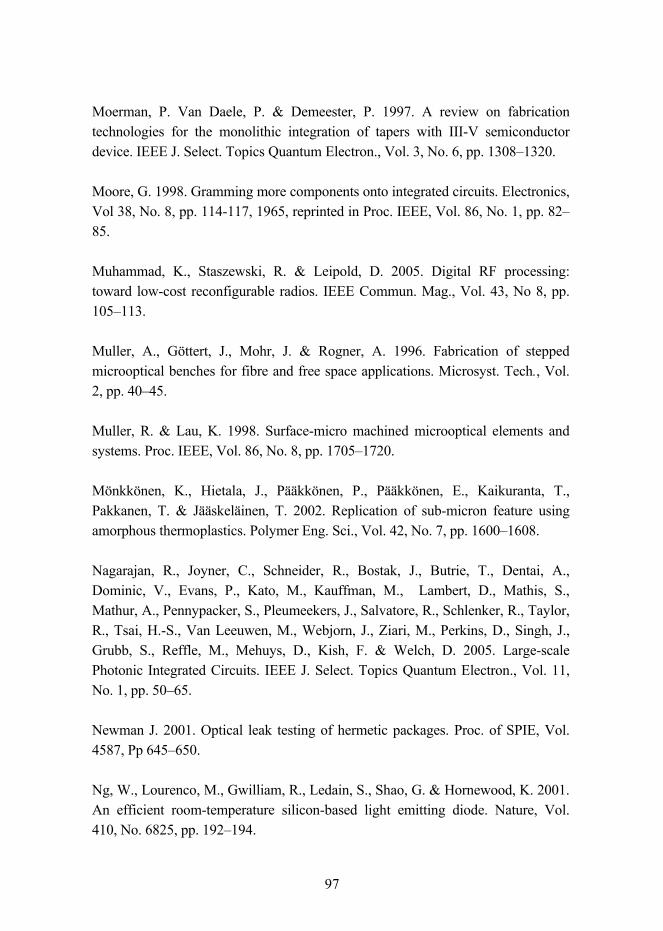
97
Moerman, P. Van Daele, P. & Demeester, P. 1997. A review on fabrication technologies for the monolithic integration of tapers with III-V semiconductor device. IEEE J. Select. Topics Quantum Electron., Vol. 3, No. 6, pp. 13081320.
Moore, G. 1998. Gramming more components onto integrated circuits. Electronics, Vol 38, No. 8, pp. 114-117, 1965, reprinted in Proc. IEEE, Vol. 86, No. 1, pp. 8285.
Muhammad, K., Staszewski, R. & Leipold, D. 2005. Digital RF processing: toward low-cost reconfigurable radios. IEEE Commun. Mag., Vol. 43, No 8, pp. 105113.
Muller, A., Göttert, J., Mohr, J. & Rogner, A. 1996. Fabrication of stepped microoptical benches for fibre and free space applications. Microsyst. Tech., Vol. 2, pp. 4045.
Muller, R. & Lau, K. 1998. Surface-micro machined microoptical elements and systems. Proc. IEEE, Vol. 86, No. 8, pp. 17051720.
Mönkkönen, K., Hietala, J., Pääkkönen, P., Pääkkönen, E., Kaikuranta, T., Pakkanen, T. & Jääskeläinen, T. 2002. Replication of sub-micron feature using amorphous thermoplastics. Polymer Eng. Sci., Vol. 42, No. 7, pp. 16001608.
Nagarajan, R., Joyner, C., Schneider, R., Bostak, J., Butrie, T., Dentai, A., Dominic, V., Evans, P., Kato, M., Kauffman, M., Lambert, D., Mathis, S., Mathur, A., Pennypacker, S., Pleumeekers, J., Salvatore, R., Schlenker, R., Taylor, R., Tsai, H.-S., Van Leeuwen, M., Webjorn, J., Ziari, M., Perkins, D., Singh, J., Grubb, S., Reffle, M., Mehuys, D., Kish, F. & Welch, D. 2005. Large-scale Photonic Integrated Circuits. IEEE J. Select. Topics Quantum Electron., Vol. 11, No. 1, pp. 5065.
Newman J. 2001. Optical leak testing of hermetic packages. Proc. of SPIE, Vol. 4587, Pp 645650.
Ng, W., Lourenco, M., Gwilliam, R., Ledain, S., Shao, G. & Hornewood, K. 2001. An efficient room-temperature silicon-based light emitting diode. Nature, Vol. 410, No. 6825, pp. 192194.
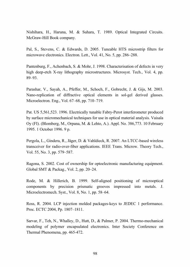
98
Nishihara, H., Haruna, M. & Suhara, T. 1989. Optical Integrated Circuits. McGraw-Hill Book company.
Pal, S., Stevens, C. & Edwards, D. 2005. Tuneable HTS microstrip filters for microwave electronics. Electron. Lett., Vol. 41, No. 5, pp. 286288.
Pantenburg, F., Achenbach, S. & Mohr, J. 1998. Characterisation of defects in very high deep-etch X-ray lithography microstructures. Microsyst. Tech., Vol. 4, pp. 8993.
Parashar, V., Sayah, A., Pfeffer, M., Schoch, F., Gobrecht, J. & Gijs, M. 2003. Nano-replication of diffractive optical elements in sol-gel derived glasses. Microelectron. Eng., Vol. 6768, pp. 710719.
Pat. US 5,561,523. 1996. Electrically tunable Fabry-Perot interferometer produced by surface micromechanical techniques for use in optical material analysis. Vaisala Oy (FI). (Blomberg, M., Orpana, M. & Lehto, A.). Appl. No. 386,773. 10 February 1995. 1 October 1996. 9 p.
Pergola, L., Gindera, R., Jäger, D. & Vahldieck, R. 2007. An LTCC-based wireless transceiver for radio-over-fiber applications. IEEE Trans. Microw. Theory Tech., Vol. 55, No. 3, pp. 579587.
Ragona, S. 2002. Cost of ownership for optoelectronic manufacturing equipment. Global SMT & Packag., Vol. 2, pp. 2024.
Rode, M. & Hillerich, B. 1999. Self-aligned positioning of microoptical components by precision prismatic grooves impressed into metals. J. Microelectromech. Syst., Vol. 8, No. 1, pp. 5864.
Ross, R. 2004. LCP injection molded packages-keys to JEDEC 1 performance. Proc. ECTC 2004, Pp. 18071811.
Sarvar, F., Teh, N., Whalley, D., Hutt, D., & Palmer, P. 2004. Thermo-mechanical modeling of polymer encapsulated electronics. Inter Society Conference on Thermal Phenomena, pp. 465-472.
99
Schift, H. & Söchtig, J. 1998. LIGA-technology for the fabrication of positioned planar surfaces. Microsyst. Tech., Vol. 4, pp. 132134.
Sugiyama, S., Khumpuang, S. & Kawaguchi, G. 2004. Plain-pattern to cross-section transfer (PCT) technique for deep x-ray lithography and applications. J. Micromech. Microeng., Vol. 14, pp 13991404.
Sunaga, Y., Takahashi, R., Tokoro, T. & Kobayashi, M. 2000. 2 GBit/s small form factor fiber-optic transceiver for single mode optical fiber. IEEE Trans. Adv. Packag., Vol. 23, No. 2, pp.176181.
Sunohara, M., Tanaka Y., Nagaoka Y., Ueda M. & Azuma K. 1987. Single lens CD player pickup system using a bi-aspheric molded glass lens. IEEE Trans. Cons. Electr. Vol CE-33, No. 4, pp. 520-530.
Taillaert, D., Bogaerts, W., Bienstman, P., Krauss, T., Van Daele, P., Moerman, I., Verstuyft, S., De Mesel, K. & Baets, R. 2002. An out-of-plane grating coupler for efficient butt-coupling between compact planar waveguides and single-mode fibers. IEEE J. Quantum Electron., Vol. 38, No. 7, pp. 949953.
Teh, N., Prosser, S., Conway, P., Palmer, P. & Kioul, A. 2000. Embedding of electronics within thermoplastic polymers using injection moulding technique. IEEE/CPMT Int. Electronics Manufacturing Technology Symposium. pp. 10-18.
Towe, E. (ed.). 2000. Heterogeneous optoelectronics integration. SPIE Press.
Tran, A., Lo, Y., Zhu, Z., Haronian, D. & Mozdy, E. 1996. Surface micro machined Fabry-Perot tuneable filter. IEEE Photon. Technol. Lett., Vol. 8, No. 3, pp. 393395.
Tummala, R. & Rymaszewski, E. (eds.). 1989. Microelectronics packaging handbook. Van Nostrand Reinhold.
Uekawa, M., Sasaki, H., Shimura, D., Kotani, K., Maeno, Y. & Takamori, T. 2003. Surface-mountable silicon microlens for low-cost laser modules. IEEE Photon. Tech. Lett., Vol. 15, No. 7, pp. 945947.
100
Wang, H., Luo, J., Shenoy, K., Royter, Y., Fonstad, C. & Psaltis, D. 1997. Monolithic integration of SEEDs and VLSI GaAs circuits by epitaxy on electronics. IEEE Photon. Technol. Lett., Vol. 9, No. 5, pp. 607609.
Wu, M. 1997. Micromachining for optical and optoelectronic systems. Proc. IEEE, Vol. 85, No. 11, pp. 18331854.
Yeung, L., Wang, J., Huang, J., Lee, S.-C. & Wu, K.-L. 2006. A compact LTCC Bluetooth system module with an integrated antenna. Int. J. of RF and Microwave CAE, Vol. 16, pp. 238244.
Yi, A., Chen, Y., Klocke, F., Pongs, G., Demmer, A., Grewell, D. & Benatar, A.. 2006. A high volume precision compression molding process of glass diffractive optics by use of micromachined fused silica wafer mold and low Tg optial glass. J. Micromech. Microeng., Vol 16, pp. 2000-2005.
Yu, W. & Yuan, X.-C. 2003. A simple method for fabrication of thick sol-gel microlens as a single-mode fiber coupler. IEEE Photon. Technol. Lett., Vol. 15, No. 10, pp. 14101412.
Appendices of this publication are not included in the PDF version. Please order the printed version to get the complete publication (http://www.vtt.fi/publications/index.jsp)
Series title, number and report code of publication
VTT Publications 692 VTT-PUBS-692
Author(s) Keränen, Kimmo Title
Photonic module integration using silicon, ceramic and plastic technologies Abstract In this work, we have developed and evaluated silicon, multilayer ceramic and plastic technologies in implementation of photonic modules utilizing passive alignment between critical devices and components. Silicon technology can provide sub-micron alignment accuracy between devices due to the lithographic manufacturing process. Silicon technology, however, is not yet capable of producing effective light sources through monolithic integration and hybrid integration has to still be applied in photonic module integration. Multilayer ceramic technology substrate is developed to provide 3 10 µm transverse alignment tolerance between laser diode and fiber in passive alignment. The achieved tolerance is adequate for multimode applications, but inadequate for single mode applications. Utilization of lithographic tooling process and light sensitive coating materials with multilayer ceramic substrates seems to be the best approach to achieve single mode tolerances in the future. In-mold integration technology utilizing bare devices assembled on substrates and using these sub-modules as inserts in injection molding process is evaluated by implementing and testing VCSEL illuminator and microscope lens for mobile phone demonstrators. Passive alignment inaccuracy below +/- 60 µm is achieved, which is adequate for the presented applications and also for many other illumination and sensing applications. ISBN 978-951-38- 7115-4 (soft back ed.) 978-951-38-7116-1 (URL: http://www.vtt.fi/publications/index.jsp)
Series title and ISSN Project number
VTT Publications 1235-0621 (soft back ed.) 1455-0849 (URL: http://www.vtt.fi/publications/index.jsp)
31130
Date Language Pages October 2008 English 100 p. + app. 72 p.
Name of project Commissioned by
Keywords Publisher device, multi-layer ceramic, plastic, substrate, module, alignment structures, passive alignment, hermetic, encapsulation, integration, injection molding, cost-efficiency
VTT P.O.Box 1000, FI-02044 VTT, Finland Phone internat. +358 20 722 4404 Fax +358 20 722 4374
VTT PU
BLIC
ATIO
NS 692
Photonic module integration based on silicon, ceram
ic and plastic...Keränen
Kimm
oESPOO 2008ESPOO 2008ESPOO 2008ESPOO 2008ESPOO 2008 VTT PUBLICATIONS 692
Kimmo Keränen
Photonic module integrationbased on silicon, ceramic andplastic technologies
In this work, we have developed and evaluated silicon, multilayer ceramicand plastic technologies in implementation of photonic modules utilizingpassive alignment between critical devices and components. Silicontechnology can provide sub-micron alignment accuracy between devicesdue to the lithographic manufacturing process. Silicon technology,however, is not yet capable of producing effective light sources throughmonolithic integration and hybrid integration has to still be applied inphotonic module integration. Multilayer ceramic technology substrate isdeveloped to provide 3 … 10 µm transverse alignment tolerance betweenlaser diode and fiber in passive alignment. The achieved tolerance isadequate for multimode applications, but inadequate for single modeapplications. Utilization of lithographic tooling process and light sensitivecoating materials with multilayer ceramic substrates seems to be the bestapproach to achieve single mode tolerances in the future. In-moldintegration technology utilizing bare devices assembled on substrates andusing these sub-modules as inserts in injection molding process isevaluated by implementing and testing HVCSEL illuminator andmicroscope lens for mobile phone demonstrators. Passive alignmentinaccuracy below +/- 60 µm is achieved, which is adequate for thepresented applications and also for many other illumination and sensingapplications.
123456789012345678901234567890121234567890123456789012345678901212345678901234567812345678901234567890123456789012123456789012345678901234567890121234567890123456781234567890123456789012345678901212345678901234567890123456789012123456789012345678123456789012345678901234567890121234567890123456789012345678901212345678901234567812345678901234567890123456789012123456789012345678901234567890121234567890123456781234567890123456789012345678901212345678901234567890123456789012123456789012345678123456789012345678901234567890121234567890123456789012345678901212345678901234567812345678901234567890123456789012123456789012345678901234567890121234567890123456781234567890123456789012345678901212345678901234567890123456789012123456789012345678123456789012345678901234567890121234567890123456789012345678901212345678901234567812345678901234567890123456789012123456789012345678901234567890121234567890123456781234567890123456789012345678901212345678901234567890123456789012123456789012345678123456789012345678901234567890121234567890123456789012345678901212345678901234567812345678901234567890123456789012123456789012345678901234567890121234567890123456781234567890123456789012345678901212345678901234567890123456789012123456789012345678123456789012345678901234567890121234567890123456789012345678901212345678901234567812345678901234567890123456789012123456789012345678901234567890121234567890123456781234567890123456789012345678901212345678901234567890123456789012123456789012345678123456789012345678901234567890121234567890123456789012345678901212345678901234567812345678901234567890123456789012123456789012345678901234567890121234567890123456781234567890123456789012345678901212345678901234567890123456789012123456789012345678123456789012345678901234567890121234567890123456789012345678901212345678901234567812345678901234567890123456789012123456789012345678901234567890121234567890123456781234567890123456789012345678901212345678901234567890123456789012123456789012345678123456789012345678901234567890121234567890123456789012345678901212345678901234567812345678901234567890123456789012123456789012345678901234567890121234567890123456781234567890123456789012345678901212345678901234567890123456789012123456789012345678123456789012345678901234567890121234567890123456789012345678901212345678901234567812345678901234567890123456789012123456789012345678901234567890121234567890123456781234567890123456789012345678901212345678901234567890123456789012123456789012345678123456789012345678901234567890121234567890123456789012345678901212345678901234567812345678901234567890123456789012123456789012345678901234567890121234567890123456781234567890123456789012345678901212345678901234567890123456789012123456789012345678123456789012345678901234567890121234567890123456789012345678901212345678901234567812345678901234567890123456789012123456789012345678901234567890121234567890123456781234567890123456789012345678901212345678901234567890123456789012123456789012345678123456789012345678901234567890121234567890123456789012345678901212345678901234567812345678901234567890123456789012123456789012345678901234567890121234567890123456781234567890123456789012345678901212345678901234567890123456789012123456789012345678123456789012345678901234567890121234567890123456789012345678901212345678901234567812345678901234567890123456789012123456789012345678901234567890121234567890123456781234567890123456789012345678901212345678901234567890123456789012123456789012345678123456789012345678901234567890121234567890123456789012345678901212345678901234567812345678901234567890123456789012123456789012345678901234567890121234567890123456781234567890123456789012345678901212345678901234567890123456789012123456789012345678123456789012345678901234567890121234567890123456789012345678901212345678901234567812345678901234567890123456789012123456789012345678901234567890121234567890123456781234567890123456789012345678901212345678901234567890123456789012123456789012345678123456789012345678901234567890121234567890123456789012345678901212345678901234567812345678901234567890123456789012123456789012345678901234567890121234567890123456781234567890123456789012345678901212345678901234567890123456789012123456789012345678123456789012345678901234567890121234567890123456789012345678901212345678901234567812345678901234567890123456789012123456789012345678901234567890121234567890123456781234567890123456789012345678901212345678901234567890123456789012123456789012345678123456789012345678901234567890121234567890123456789012345678901212345678901234567812345678901234567890123456789012123456789012345678901234567890121234567890123456781234567890123456789012345678901212345678901234567890123456789012123456789012345678123456789012345678901234567890121234567890123456789012345678901212345678901234567812345678901234567890123456789012123456789012345678901234567890121234567890123456781234567890123456789012345678901212345678901234567890123456789012123456789012345678123456789012345678901234567890121234567890123456789012345678901212345678901234567812345678901234567890123456789012123456789012345678901234567890121234567890123456781234567890123456789012345678901212345678901234567890123456789012123456789012345678123456789012345678901234567890121234567890123456789012345678901212345678901234567812345678901234567890123456789012123456789012345678901234567890121234567890123456781234567890123456789012345678901212345678901234567890123456789012123456789012345678123456789012345678901234567890121234567890123456789012345678901212345678901234567812345678901234567890123456789012123456789012345678901234567890121234567890123456781234567890123456789012345678901212345678901234567890123456789012123456789012345678
ISBN 978-951-38-7115-4 (soft back ed.) ISBN 978-951-38-7116-1 (URL: http://www.vtt.fi/publications/index.jsp)ISSN 1235-0621 (soft back ed.) ISSN 1455-0849 (URL: http://www.vtt.fi/publications/index.jsp)
Julkaisu on saatavana Publikationen distribueras av This publication is available from
VTT VTT VTTPL 1000 PB 1000 P.O. Box 1000
02044 VTT 02044 VTT FI-02044 VTT, FinlandPuh. 020 722 4520 Tel. 020 722 4520 Phone internat. + 358 20 722 4520
http://www.vtt.fi http://www.vtt.fi http://www.vtt.fi