Embed Size (px)
Citation preview

UNITED STATES MILITARY ACADEMY
2009 Program Review
Photonics Research Center
United States Military Academy West Point, NY 10996


iii
THE PHOTONICS RESEARCH CENTER
Bi-Annual Research Program Review 2007 – 2009
Director’s Message
The Photonics Research Center has advanced into the second decade of service to the United States Army. Established by a memorandum of understanding between the Superintendent of the Military Academy and the Vice Chief of Staff of the Army, the Center has three principal missions: educate future Army leaders, conduct basic research, and support the Army and the Department of Defense in the areas of lasers and photonic technologies. This report summarizes the research and education efforts of the Photonics Research Center from the last report in April, 2007 to November, 2009. This report is produced in partial fulfillment of a bi-annual program review conducted by the Army Research Office, the Center’s major funding agency. The personnel situation within the center has begun to slowly stabilize over the past two years. Since the last review, the previous Director of the Center, LTC John Hartke took over the core Physics Program and has been decisively engaged with the administration of that critical program within the Department of Physics. While LTC Hartke is actively engaged in that program, LTC Walter Cole became the principal investigator for the Department of Physics after arriving to the center upon completion of his Ph.D. in the Optical Sciences. LTC William F. Pearman arrived back at West Point in January of 2008 after completing his Ph.D. in Analytical Chemistry. LTC Pearman filled the position previously vacated by LTC(R) Fountain as the Chemistry and Life Science principal investigator and the sixth Academy Professor assigned to the Center in its history. LTC Pearman assumed the duties as the Director of the Center in June of 2008. In 2007, LTC Jim Raftery vacated the Department of Electrical Engineering and Computer Science’s (D/EECS) principal investigator position in the PRC to serve as the Army's Product Manager (PM) for Information Warfare. LTC Greg Kilby moved from Department of Electrical Engineering and Computer Sciences (EECS) to fill the vacancy. In 2008, LTC Raftery was selected as the seventh Academy Professor assigned to the center and is scheduled to return to fill the Academy Professor position in 2011 after completing his PM duties and The Army War College.
Our researchers continued to engage cadets in our primary mission of educating future Army officers in the area of photonics. The Center received a grant from the High Energy Laser Joint Technology Office in support of the teaching mission. The number of cadets performing research in the Center has steadily increased over the past two years. A multidisciplinary team of cadets placed third in the Soldier Design Competition held at Massachutes Institute of Technology in 2008. Cadet Gee, working with the chemistry cell, received the 2009 Undergraduate Student Award from the New York Section of the Society for Applied Spectroscopy (NYSAS) for his spectroscopy work.
Most importantly, the Center and its personnel continue to provided outreach and expertise in laser related technologies across the Army and the Department of Defense in research efforts in support of the Joint Technology Office, ARDEC, and JIEDDO among others. LTC Pearman continues to serve as a subject matter expert (SME) and has evaluated numerous systems and spectroscopic techniques for counter improvised explosives devices (CIED) support the deployed Army. Furthermore, the center is participating in the program to redesign a more effective camouflage pattern for Operation Enduring Freedom by providing both equipment and spectroscopic expertise.
The research accomplishments highlighted in this report represents the products of a healthy, mature research organization focused on educating our future Army leaders and closing the technology gaps in the area of photonics. They are the result of hard work and are a tribute to the extremely talented researchers, cadets, and support staffs that are associated with the Center.
William F. Pearman, Ph.D. Lieutenant Colonel, Academy Professor Director

iv
THE PHOTONICS RESEARCH CENTER
Center Overview The Photonics Research Center is entering its twenty third year of service at the United States Military Academy. It was established at West Point in May of 1987 through a Memorandum of Understanding between the Superintendent of the United States Military Academy and the Vice Chief of Staff of the Army. An excerpt from this memorandum provides some insight into the charter of the Center:
“As the Army modernizes in an increasingly complex technological environment, it is essential that Army officers understand the advanced technologies which form critical elements of our evolving weapons systems. One technology field which is already exerting a major influence on force planning, and whose impact is certain to grow over the next two decades, is the physics and engineering of lasers, and the technologies associated with their development and applications. The Army needs a strong base of research and development in laser-related fields. It also needs an officer corps generally familiar with laser technologies and a subset of that officer corps whose members are experts in developing and applying those technologies.”
The Photonics Research Center is comprised of researchers from the Departments of Chemistry and Life Science, Electrical Engineering and Computer Science, and Physics who conduct basic and applied research using lasers and laser technology. The Center's three primary missions focus on education of both cadets and officers, the conduct of basic and applied research, and support to the Army in the area of lasers and photonics. Funding support for the Center is provided through the Physics Division of the Army Research Office. Each year, educational programs associated with the Photonics Research Center introduce over 1000 cadets to a general familiarity with laser technology, provide over 50 cadets with an in-depth understanding of lasers and laser technology, and return several officers to the Army who are now considered experts in developing and applying laser technologies. In the area of basic and applied research, the Center maintains upwards of eight active research experiments producing both faculty and student conference presentations and technical journal articles. Specific research areas include surface-enhanced Raman spectroscopy, laser-induced carbonization of polymers, non-linear optics and optical limiting, optical information processing, interferometry, hyperspectral imaging, atmospheric effects on laser propagation, and remote sensing. Additionally, the Center has provided direct support to the Army and DoD agencies in the form of technical support to Program Manager – Kuwait Iraq C4 Commercialization (PM-KICC) and the Joint Improvised Explosive Device Defeat organization (JIEDDO). The Center has also hosted scientist from Baghdad University as part of the Academy’s outreach to the educators in Iraq. Finally, the Center has increased its interaction with the Army research and development enterprise by increasing collaboration with the Army Research Laboratory as well as other DoD organizations.

v
Photonics Research Center Staff and Faculty
2007 – 2009 Board of Directors COL David C. Allbee, Ph.D. in Physical Chemistry, Pennsylvania State University, 1985, Professor and Head, Department of Chemistry and Life Science. COL Eugene K. Ressler, Ph.D. in Computer Science, Cornell University, 1993, Professor and Head, Department of Electrical Engineering and Computer Science. COL Edward P. Naessens, Jr., Ph.D. in Nuclear Engineering, Rensselaer Polytechnic Institute, 1999, Professor and Head, Department of Physics. Academy Professors COL Barry L. Shoop, Ph.D. in Electrical Engineering, Stanford University, 1992, Professor of Electrical Engineering, Department of Electrical Engineering and Computer Science. LTC John Hartke, Ph.D. in Optical Sciences, The University of Arizona, 2005, Associate Professor (Photonics), Department of Physics. COL Robert W. Sadowski, Ph.D. in Electrical Engineering, Stanford University, 1995, Associate Professor (Photonics), Department of Electrical Engineering and Computer Science. LTC William F. Pearman, Ph.D. in Analytical Chemistry, University of South Carolina, 2007, Academy Professor, Department of Chemistry and Life Science. Title X Civilians Thomas M. Spudich, Ph.D. in Analytical Chemistry, Northern Illinois University, 1999, Assistant Professor, Department of Chemistry and Life Science. Wenli Huang, Ph.D. in Electrical Engineering, University of Connecticut, 1995, Professor of Electrical Engineering, Department of Electrical Engineering and Computer Science. Rotating Military Faculty LTC Walter P. Cole, Ph.D. in Optical Sciences, Air Force Institute of Technology, 2008, Department of Physics. MAJ John D. Delong, MS in Optics, University of Rochester, 2007, Department of Physics. LTC John M. Ingram, MS in Physical Chemistry, University of Idaho, 1999, Department of Chemistry and Life Sciences. LTC Gregory R. Kilby, Ph.D. in Electrical Engineering, Georgia Institute of Technology, 2005, Department of Electrical Engineering and Computer Sciences. MAJ Walter D. Zacherl, MS in Applied Physics, Stanford, 2007, Department of Physics. Administration Telephone numbers: Commercial (845) 938- xxxx or DSN 688-xxxx
Director LTC William Pearman Laboratory Facilities Manager Mrs. Andrea E. Sanborn Budget Assistant and Administrative Officer: Mrs. Carrol Piatt-Southard
Photonics Research Center Bartlett Hall, Building 753, Room B21 MADN-PRC West Point, New York 10996 General Information x-3739 Facsimile x-3062 Director x-4013 Facilities Manager x-8705 Administrative Assistant x-2624

vi
Table of Contents
Director’s Message ................................................................................................................. iii Center Overview .................................................................................................................... iv
Photonics Research Center Staff and Faculty ...................................................................... v
Department of Chemistry & Life Science ............................................................................. 1 Surface-Enhanced Raman Spectroscopy of Saxitoxins: Exploratory Studies ................................................... 2 Hyperspectral Imaging to Develop Adaptable Near Infrared Camouflage ..................................................... 10 Development of an Identification Friend or Foe Emitter Using the Laser Carbonized Light Emitting Filament .......................................................................................................................................................... 18
Department of Electrical Engineering & Computer Sciences .......................................... 29 VLSI Electronics for Photonic Image Processing, Smart Pixel Technology and Optical A/D Conversion.... 30 Minimization of color halftone texture visibility using three-dimensional error diffusion neural network .... 41 Photonic Crystal Vertical-Cavity Surface-Emitting Laser Research .............................................................. 54 Cadet Capstone Design and Independent Study Projects ............................................................................... 62 Project 1: Electronic Laser Instrument ........................................................................................................... 63 Project 2: Optical Coherence Tomography ..................................................................................................... 66 Project 3: Target Location and Direction Module .......................................................................................... 69 Project 4: IED Employment and Initiation ..................................................................................................... 70 Cadet Extracurricular Activities at the PRC – The Electronics Experimental Club ....................................... 71
Department of Physics .......................................................................................................... 72
Electronic Speckle Pattern Interferometry for Atmospheric Phase Disturbances ........................................... 73 Analysis of the Joint High Power Solid State Laser for Neutralization of an 81mm Mortar Threat .............. 85 Optical Signatures and Atmospheric Effects on Laser Propagation ............................................................... 88 Characterization of Non-linear Optical Materials Through Double Pump-Probe Measurements .................. 94
PRC Principle Investigator Biographical Information ................................................... 100
Walter Cole ................................................................................................................................................... 101 John Hartke ................................................................................................................................................... 102 Wenli Huang ................................................................................................................................................. 103 John M. Ingram ............................................................................................................................................. 104 Gregory R. Kilby .......................................................................................................................................... 105 William F. Pearman ...................................................................................................................................... 106 Robert W. Sadowski ..................................................................................................................................... 107 Barry L. Shoop.............................................................................................................................................. 108

1
Department of Chemistry & Life Science
2
Surface-Enhanced Raman Spectroscopy of Saxitoxins: Exploratory Studies
William F. Pearman*1 and Sherwood Hall**
*Department of Chemistry and Life Science, United States Military Academy, West Point, NY, 10996
**Food and Drug Administration, HFS-716, CHCB DBC ORS CFSAN, College Park, Maryland 20740
Abstract Saxitoxins are a family of toxins produced by cyanobacteria and dinoflagellates that are
found in both harmful algal blooms (HAB) in the world’s oceans and in freshwater lakes. Previous published work established the feasibility of Surface Enhanced Raman Spectroscopy as a viable method for the detection and quantification of the parent toxin, Saxitoxin. Current studies are focused on three saxitoxin derivatives (two 11-hydroxysulfate (GTX2, GTX3) and one N-1- hydroxyl (NEO)). These studies include both the spectral identification of the individual derivatives using SERS and the possible classification of the each derivative using multivariate statistical techniques. Background
Saxitoxins are a family of toxins produced by cyanobacteria and dinoflagellates1 that are found in both harmful algal blooms (HAB) in the world’s oceans2 and in freshwater lakes1,3 of which Saxitoxin is the nominal parent. Saxitoxins are naturally produced algal toxins (marine or fresh water) that are often associated with shellfish bed closings and surface water contamination during harmful algal blooms.1,2,4 Human exposure to this deadly toxin, mostly through the consumption of contaminated shellfish5, can lead to paralysis, respiratory failure, and/or death. Aside from the obvious health related concerns generated by this toxin, there are also environmental (fish kills, shellfish contamination) and economic (commercial fisheries, recreation and tourism) impacts to consider.6
To date several analytical techniques have been utilized to detect saxitoxin. These
techniques can be separated into two broad, if not overlapping categories; bioassay and spectroscopic techniques. The current standard for the detection and quantification of aqueous saxitoxin is the mouse injection assay7 which, though accurate, it is impractical for on site applications and hampered by the need for a large number of live animals.
Raman spectroscopy, specifically Surface Enhanced Raman Spectroscopy (SERS), is an effective technique for the non-invasive analysis of biologically relevant molecules.8 The normal Raman effect is very weak where only one in ~109 photons will be inelastically or Raman scattered. However, SERS significantly enhances the detectable Raman signal by several orders of magnitude through both electromagnetic and chemical enhancement factors. It is also a rapid technique requiring little sample preparation. Thus, a major benefit of SERS is the ability to qualify and quantify molecules at biologically relevant concentrations in near real time.8 Previous work demonstrated the feasibility of using SERS for the detection and quantification of

3
saxitoxin.9 The current work focuses on studies of three saxitoxin derivatives (two 11-hydroxysulfate (GTX2, GTX3) and one N-1- hydroxyl (NEO)) for SERS analysis. The structures for GTX2, GTX3, and NEO are shown in Figure 1 below.
Figure
1.
Structures
of GTX2 (a), GTX3 (b), and NEO (c)
Experimental Materials Stock saxitoxin solution were made by dissolving solid saxitoxins in 3 mM HCl. All saxitoxin samples were provided by the United States Food and Drug Administration (USFDA). NaBH4, 30% H2O2 and AgNO3 were purchased from Sigma and H2SO4 purchased from Fisher Scientific. All reagents were used without further purification or modification. All samples and dilutions were prepared in pure water Instrumentation An Argon Ion Laser operating at both 514 and 488nm was used as the excitation source for this study. The laser energy was delivered to the sample vials via a fiber optically coupled, focused Raman probe (InPhotonics Raman Probe). The collection fiber from the Raman Probe was coupled to a .5m spectrometer. Raman spectra were recorded using a 16-bit, TE cooled, CCD. Daily calibrations of the system were performed using cyclohexane. Colloidal particle sizing was performed via dynamic light scattering (Brookhaven Instruments Corp., ZetaPlus Particle Sizing). Finally, UV/VIS spectra of the Ag colloid were obtained using a Lamda 19 UV/Vis Spectrometer.
a) b) c)

4
Borohydride Stabilized Ag Colloidal Synthesis All glassware was cleaned using a 4:1 H2SO4:30% H2O2 solution prior to colloid
synthesis. Borohydride stabilized particles were prepared using a slightly modified procedure originally described by Cermakova et al.10 Briefly, 150 mL of 1.2 mM NaBH4(aq) was placed in a 250 mL round bottom flask submerged in an ice bath. 20 mL of 2.2 mM AgNO3(aq) were prepared in a separate flask and also chilled in an ice bath. After approximately one half hour, a stir bar was added and the NaBH4 solution was vigorously stirred. The AgNO3 was then added drop wise with the use of a disposable pipette to the NaBH4. The balance of the AgNO3 solution remained in the flask in the ice bath until use. Once added, the drops would turn dark gray, disperse in the NaBH4, ultimately turning the bulk of the solution a pale yellow. Once all of the AgNO3 was added, the colloidal solution was removed from the ice bath and stirring was continued for an additional 45 minutes. The hydrosol used herein was synthesized for a previous, unrelated experiment and was stored for a period of three months prior to use in this study.
Sample preparation Aqueous dilutions of the stock saxitoxin solutions were performed prior to addition to the Ag colloidal hydrosol. Standard half dram sample vials (Fisher Scientific) were used for both the preparation and the collection of SERS spectra. The SERS samples were all prepared with 800µL of borohydride reduce silver nanoparticles (AgNPs) that had aged for several weeks. To the AgNP, a 20µL aliquot of a stock toxin solution was added and vortex mixed for 2 seconds. The final toxin concentrations were on the order of 40 µM. Results and Discussion 514nm Excitation To test the SERS response for the individual toxins (GTX2, GTX3, and NEO) at 514nm, SERS spectra were collected and analyzed for each toxin. The SERS samples were prepared as detailed above and after mixing, the sample vial was placed into the sample holder and irradiated for 10 minutes at 40mW prior to the collection of any SERS data. This approach minimized the influence of adsorption kinetics on the measured SERS spectra. Each SERS spectrum was recorded with 6 acquisitions of 10 seconds each and 5 replicate samples were analyzed for each toxin. Removing the contribution of adsorption kinetics allowed for the collection of fairly reproducible SERS spectra for the individual toxins. Collecting the SERS response at times <5 minutes introduced significant fluctuations in the SERS spectra. Therefore, a delay of 10 minutes was used to minimize these fluctuations. The individual SERS spectra for GTX2, GTX3, and NEO are shown in Figure 2.

5
a) b)
c)
Figure 2. SERS spectra of GTX2 (a), GTX3 (b), and NEO (c) collected at 40mW, 514nm excitation.
It is interesting to note that there are slight differences between the SERS spectra of
GTX2 and GTX3, two stereo isomers. Reviewing the 514nm data, there appears to be two particular regions of note for identifying the spectral differences between GTX2 and GTX3. These regions are around 825cm-1 and between 1300 – 1425cm-1. The general trends are shown in Figure 3.
Figure 3. Average SERS spectra for GTX2 (black) and GTX3 (red) and the observed trends between the two toxins (red and black arrows). The blue arrow and bracket denote the spectral regions of interest.

6
In Figure 3, the red trace is for the SERS response of GTX3 and the black trace is for GTX2. The arrows are colored by their observed trends in the SERS spectra, i.e. red arrow shows trends for GTX3 and black is indicative of trends for GTX2.
Not surprisingly, multivariate analysis of the spectral data of the 15 different spectra from
the three different toxins also show clear separation in both principal component space and in cluster analysis as shown in Figure 4.
Figure 4. Multivariate analysis of SERS data obtained from 514nm excitation.
In both of the plots shown in Figure 4, the SERS data was both normalized and mean centered prior to analysis. Additionally, the data was analyzed using three principal components which captured 99.12% of the variance in the data. 488nm Excitation The same sample preparation protocols from the study using 514nm excitation were followed in a separate study using new toxin samples and 488nm excitation. For all SERS data collected all experimental parameters were identical to that of the 514nm study with the exception of the laser energy. For the 488nm study, 50mW of laser energy was used. According to theory, the SERS response should be independent of laser excitation wavelength and thus should serve as a means of confirming the trends and overall SERS response observed in the 514nm study. The individual SERS spectra obtained at λex = 488nm are shown in Figure 5. As with the NEO 514nm SERS samples, there was little measured difference with the SERS response for NEO at 488nm when compared to both GTX2 and GTX3. This is most likely due to the rquick adsorption of NEO to the colloidal surface as indicated by a color change of the AgNPs upon the addition of NEO to the colloidal suspension.

7
a) b)
c)
Figure 5. SERS spectra of GTX2 (a), GTX3 (b), and NEO (c) collected at 50mW, 488nm excitation.
Once again analysis of the SERS spectra under 488nm excitation using principal
component analysis shows good separation of the three toxins in the study as shown in Figure 6.
Figure 6. Multivariate analysis of SERS data obtained from 514nm excitation.
In both of the plots shown in Figure 6, the SERS data was both normalized and mean centered prior to analysis. Additionally, the data was analyzed using only two principal components which captured 99.29% of the variance in the data.

8
Comparison of 514 and 488nm SERS Data The SERS response under the two wavelengths used in this study holds true to the theory in terms of the independence from the excitation wavelength. There are some slight intensity differences in the 488nm data that do not appear in the 514nm data. The data currently supports a possible near-resonance condition with the 488nm excitation. Careful examination of the UV/Vis data shows a new feature around 351nm in the AgNP/GTX3 sample after 488nm radiation that is not pronounced or present in the AgNP or AgNP/GTX3 sample prior to exposure to laser radiation (Figure 7)
a) b)
Figure 7. UV/Vis data from GTX3 and AgNPs. UV/Vis data (a) from the AgNPs only (green), AgNPs/GTX3 prior to 488nm excitation (red), and AgNPs/GTX3 after exposure to 488nm excitation (black). 7.b shows the first derivative plot of the AgNPs/GTX3 after exposure to 488nm excitation Taking the average spectrum from both the 514nm and 488nm study and placing them on
the same graph (Figure 8) also clearly shows the spectral similarities for the three toxins analyzed in this study.
a) b)
c)
Figure 5. Average SERS spectra of GTX2 (a), GTX3 (b), and NEO (c) collected at 514nm (red) 488nm (black) excitation.

9
Finally, it does not appear that the spectral differences around 825cm-1 transfer well
between the two different excitation wavelengths, however the bands between 300 – 1425cm-1 do remain consistent between the two excitation wavelengths. Conclusion It is clear through this study that SERS can provide powerful qualitative information and discrimination amongst structurally similar toxins. The main issue of substrate reproducibility is the focus of future studies. The AgNPs must meet specific conditions to achieve or introduce adsorption of the toxins to the AgNP surface have yet to be qualified. Due to the age of the SERS active colloids, it appears that aggregation of the AgNPs is the most likely cause for the SERS response. The SERS response of the mature colloids versus the lack of any SERS response for freshly prepared colloids is also indicative of aggregation. However, once the colloidal conditions are qualified, the ability of SERS to discriminate amongst structurally similar members of a specific class of toxins is very promising for future applications Bibliography 1. Newcombe, G.; Nicholson, B., Treatment options for the saxitoxin class of cyanotoxins. Water Science & Technology: Water Supply 2002, 2 (5-6), 271-275. 2. K. G. Sellner, G. J. D., and G. J. Kirkpatrick, J. Ind. Microbiol. Biotechnol. 2003, 30, 383. 3. Kaas, H.; Henriksen, P., Saxtioxins (PSP Toxins) in Danish Lakes. Water Research 2000, 34 (7), 2089-2097. 4. M. C. Louzao, M. R. V., J. M. V. Baptista de Sousa, F. Leira, and L. M. Botana, Anal. Biochem. 2001, 289, 246. 5. M. A. Quillian and J. L. C. Wright, Anal. Chem. 1989, 61 (18), 1053A. 6. P. Hoagland, D. M. A., Y. Karoru, and A. W. White, Estuaries 2002, 25 (4b), 819. 7. AOAC Official Method 959.08, P. S. P. 8. Pearman, W. F.; Lawrence-Snyder, M.; Angel, S. M.; Decho, A. W., Surface-Enhanced Raman Spectroscopy for in Situ Measurements of Signaling Molecules (Autoinducers) Relevant to Bacteria Quorum Sensing. Applied Spectroscopy 2007, 61, 1295-1300. 9. Pearman, W. F.; Angel, S. M.; Ferry, J. L.; Hall, S., Characterization of the Ag Mediated Surface-Enhanced Raman Spectroscopy of Saxitoxin. Applied Spectroscopy 2008, 62, 727-732. 10. Cermakova, K.; Sestak, O.; Matejka, P.; Baumruk, V.; Vlckova, B., Surface-Enhanced Raman-Scattering (Sers) Spectroscopy with Borohydride-Reduced Silver Colloids - Controlling Adsorption of the Scattering Species by Surface-Potential of Silver Colloid. Collection of Czechoslovak Chemical Communications 1993, 58 (11), 2682-2694.

10
Hyperspectral Imaging to Develop Adaptable Near Infrared Camouflage
LTC William F. Pearman1, LTC John Ingram2, Cadet Noah Kim1 and Cadet Sungjin Song1and Betsy Moore3
1Photonics Research Center and the Department of Chemistry and Life Science, United States Military Academy, West Point, NY, 10996 , 2United States Military Academy, West Point, NY
10996 Currently with CENTCOM, Tampa, FL 3Marine Corps Systems Command Combat Equipment Support Equipment Program Manager
Infantry Combat Equipment, 2200 Lester Street Quantico, VA 22134-6050
Abstract
The availability of commercial and surplus military night vision optics utilizing generation I and II (GEN I & II) light intensifying technologies has caused an increase in concern of the spectral qualities of camouflage, specifically the near infrared. A field expedient appliqué which allows individuals to match the background spectral response in the NIR can significantly reduce the possibility of detection. Initial studies utilized COTS products applied to different patterns and clothing materials and were evaluated with both hyperspectral imaging and GEN II night vision devices. These early results indicated that it was possible to use a NIR absorber to alter the NIR reflectance of the materials, thus decreasing the overall probability of detection. Current research is directed towards the identification of NIR materials, potentially both absorbers and fluorescers that can achieve the desired effect of matching the spectral background across both the visible and NIR without irreparable damage to the clothing material. The use of such appliqués would allow individuals, with specific mission sets, to apply and assess the effectiveness of these appliqués in the operational area.
Background Hyper-spectral imaging (HSI) is a powerful sensing technology. Its strength lies in the camera’s ability to collect banded spectrum data over a defined area rapidly. HSI output data contains complete banded spectra for each pixel (Figure 1). These individual spectra can be manipulated using any number of algorithms designed for imaging the specific target. HSI output data can be viewed as a two dimensional array like a regular digital photo.
HSI has several advantages over point spectrometer or color pictures. The captured HSI scene contains all the information for calibrating and comparing unknown materials and the background reflectance. There are no errors in color matching because all the information is collected simultaneously. One 30 second scan can provide all the information needed to match test materials against the background under those lighting conditions.
Current hyper-spectral imaging has several limitations. The major drawback is that the HSI image must be collected on site with natural lighting and background. Simulated or modeled background would more than likely miss many subtleties of an actual outdoor scene. The individual spectra are banded resulting in relatively low resolution of individual spectral features. In this application, however, only broad peak identification is needed for imaging purposes. Another weakness to hyper-spectral imaging is that the complete data package is very

11
large. One 640x640 pixel hyper-spectral image is almost 100MB. For our post picture analysis, this is a small limiting factor.
x
yλ
x
yλ
Figure 1: Hyperspectral Data Cube
HSI is a rapidly expanding technology. HSI sensors are being used in many high altitude
applications from measuring water content in soil to assessing different tree species in Finland to identifying mineral concentrations in the Californian deserts. Most space exploratory vehicles have an integrated HSI or multispectral sensing system. Hyper-spectral imaging is being used in agriculture to quickly assess produce for disease and ripeness. The technology has been incorporated into microscopes to conduct micro analysis on chemical composition of pharmaceuticals. HSI systems are sold commercially with coverage in increments from UV/VIS to LWIR.
The goal of this project was to use Hyperspectral imaging to provide technical evaluation
of camouflage materials and household application sprays with the overall goal to answer the question “What is the best combination of materials and application sprays to create adaptable camouflage in the NIR (600-800nm)?” Experimental Materials
Several COTS items were purchased from the Post Exchange that spanned across several different classes of products. They included spray paints, (Krylon Camo Spray Paint and Krylon Clear Spray Paint), deodorants (Sure and Gillette), and hair spray (Suave and Aqua Net). The

12
materials are depicted in Figure 2. A NIR absorbing COTS dye was purchased from Fabric Holding Inc.
Figure 2: COTS products used in initial study
Instrumentation The Hyper-spectral imager used in the study was a OKSI Hyperscan VNIR. The Hyperscan VNIR is a Push-Broom type imager with a spectral range from 390-1060 nm with 520 bands (1.29 nm resolution). Two lenses (70mm and 35mm) are available for use with the system. The spectral data is analyzed using ENVI software (ITT Visual Information Solutions). Illumination in the laboratory was provided by a 1000 W Oriel Research Quartz Tungsten Halogen (QTH) lamp.
Results and Discussion Black Control Fabric
The initial study developed controlled experiments to determine the near infrared (NIR) signature of materials and sprays in a laboratory environment. The COTS products could then be identified as either infrared (IR) absorbers or fluorescers. A swath of black cotton was used as the control sample for the evaluation of these COTS products. The COTS products were applied to the black material and the HSI data was collected and then evaluated using the ENVI software. The results from these experiments are found in Figure 3. For the products tested, on the Sure product produced a more intense IR signal than the control fabric swath.

13
37
39
41
43
45
47
49
51
53
745 765 785 805 825 845
Arb
irta
ry R
efer
ence
Wavelength (nm)
Experimental Data on Black Control Fabric
Sure
Control
Gillette
Krylon Clear
Aqua Net
Krylon Camouflage
Figure 3. NIR results from initial tests for COTS products on black control fabric.
MARPAT 50/50 Material Following the same protocols and experimental design, the same COTS products were tested in the Marine Corps camouflage pattern (MARPAT) on the standard 50/50 cotton blend fabric. The results from these experiments are shown in Figure 4. Although the Kylon Camouflage paint did significantly reduced the NIR signature; it in essence destroyed the visible properties of the material as well – turning the whole uniform brown.
40
45
50
55
60
65
70
75
80
740 760 780 800 820 840 860
Arb
itra
ry R
efer
ence
Wavelength (nm)
MARPAT Laboratory Data
Sure
MARPAT (control)
Krylon Clear
Gillette
Suave
Aqua Net
Krylon Camouflage
Figure 4. NIR results from initial tests for COTS products on MARPAT fabric.
The MARPAT camouflage was then evaluated against a natural background, to determine if the MARPAT NIR signature needed to be increased or reduced for those particular

14
background conditions. Then, based upon laboratory data, apply the COTS products in an attempt to tailor the NIR signature of the MARPAT material to match the background.
50
55
60
65
70
75
80
740 760 780 800 820 840 860 880 900
Arb
itra
ry R
efer
ence
Wavelength (nm)
MARPAT Field Test
MARPAT blouse (untreated)Background
MARPAT Blouse (Aqua Net Treated)
Figure 5. NIR results from initial tests for COTS products on MARPAT fabric.
The results shown in Figure 5 showed promise into the prospect of applying an appliqué that could not only reduce the overall NIR response of the MARPAT material, but could be applied to match the spectral response of the background. Assessment of a COTS IR Absorbing Dye Instead of attempting to identify the IR absorbing materials in the COTS products discussed earlier, the evaluation of an NIR absorbing fabric dye was evaluated. The UV/Vis spectrum for once such dye is shown in Figure 6. The optimum NIR absorbing dye needs to have little absorbance in the visible while possessing a peak absorbance in the NIR. This particular dye has an overall greenish tint, so it could also serve the purpose of reducing the spectral reflectance in the visible as well.

15
Figure 6. Absorbance spectrum from a COTS NIR absorbing dye.
Three different camouflage patterns were evaluated on a similar fabric base. The three patterns were the MARPAT, the Universal Camouflage Pattern (UCP) for the Army Combat Uniform (ACU), and Multicam. The bottom half of each fabric swath as sprayed with a diluted solution of the COTS dye from Figure 6. The RGB representation from the HSI data is shown in Figure 7.
a) b) c)
Figure 7. RGB representation from the HSI image collected from three different patterns a)
MARPAT, b)UCP, and c) Multicam.

16
A single HSI image was collected of all three swaths of fabric at one time and therefore under identical lighting conditions. Five regions of interest (ROIs) were selected for the areas of the fabric without the dye and five ROIs were evaluated on the area of the fabric where the dye had been applied. The ROIs were selected to give an average response across the whole pattern and thus no consideration was given to selecting ROIs on regions of the patterns that possessed the same colors. The average spectra for these ROIs is shown in Figure 8.
a) b)
c)
Figure 8. Average reflectance spectra for 5 ROIs without dye (black) and 5 ROIs with dye applied (red) for the three different patterns shown in Figure 7.
Clearly there was a reduction in both the visible and NIR regions for all three samples. However, the MARPAT showed the least amount of visible change. Additionally, the underlying patters of the MARPAT were still visible even under observation from GEN II night vision optics. This can be better seen in Figure 9 where images of the MARPAT swath were collected via a standard digital camera and by the same camera through two different night vision optics. It is difficult to see in these images, but by eye through the night vision optics, the patterning of the MARPAT is clearly visible. This experiment needs to be conducted against a natural background. However, the possibility exists for the underlying patterning of the material to act as the NIR reflector, while a applied dye would serve as the NIR absorbing material.

17
a) b) c)
Figure 9. Digital camera images collected a) normally, b) through a AN/PVS7D, and c)
through AN/AVS6V(I) night vision optics. Conclusions There does exist the possibility for individual service members, with specific mission sets, to tailor the NIR spectral properties of their individual equipment. There is a significant amount of research to pursue to achieve this possibility. However, from the very basic beginnings of applying COTS products from the post exchange, the potential to advance this concept though basic science and spectroscopic measurements is very intriguing.

18
Development of an Identification Friend or Foe Emitter Using the Laser Carbonized Light Emitting Filament
Dr. Thomas M. Spudich, LTC Gregory R. Kilby, LTC John M. Ingram1
Department of Chemistry and Life Science, and Department of Electrical Engineering and Computer Science Photonics Research Center
United States Military Academy, West Point, NY 10996 1Currently with CENTCOM, Tampa, FL
The Photonics Research Center has worked on laser pyrolized polyimide films for almost twenty years, and research has included both fundamental science and material applications.(1-8) The overall goal of this research project is utilize these pyrolized polyimide films in developing a small, high output mid/longwave infrared (IR) emitter, in 4-12 micron region of the spectrum, which could be integrated into an individual friend or foe (IFF) device. The unique IR emission characteristics of these laser pyrolized filaments and have been demonstrated. Their relatively high intensity in the mid/longwave IR region enhances their potential for use in an IFF device, but there is still room for improvement in both design and fabrication. The first prototype provided identification out to 50 meters using an AN/PAS 13B heavy. The advantages of the current design are the extremely low cost, ease of assembly, and relatively low power consumption.
Background Kapton is a condensation product of pyrometallic dianhydride and p,p’-oxydianiline. Prior research has shown that, when exposed to a continuous wave, argon-ion laser, the Kapton undergoes pyrolysis as seen below in Figure 1. This pyrolysis process involves UV laser radiation that creates a carbon pattern on the surface of the Kapton without significantly changing the shape of the film. A computer aided design program works in conjunction with the laser to produce the pattern. The carbon pattern conducts an electric current when attached to a power supply.
Figure 1. Reaction associated with the pyrolysis of Kapton with an argon ion laser.(6)
Research has shown that the pyrolized Kapton emits a very intense thermal image compared to other blackbody radiators. The thermal emission of the Kapton filament may prove to be very useful if the emission spectrum could be characterized. The pyrolized Kapton was compared with other blackbody emitters in this process, to include resistors. Rationale for this type of work includes a wide variety of military law enforcement applications, including functioning as an IFF device in the field if Key Performance Parameters can be met and these parameters are listed in Table 1.
NN
O
O
O
O
O
n
λ = 488 nm & 514 nm C(s) (96%) + CO(g)
+ CO2(g) + C2H2 (g) + HCN (g) + N2H4(g) + CH4(g)

19
Table 1. Simplified Key Performance Parameter list from proposed IFF requirements document. LEF is the designation for the initial IFF prototype produced by the PRC.
KPP Target Optimal IFF Distance 300 meters 1000 meters Wavelength 8-12 microns Weight 6 oz < 4 oz # of Emitters 5 omni-directional 1 omni-directional Cost $350/unit
This work will focus on the characterization of the Kapton filament emission and building of an IFF device. Experimental Pyrolysis Procedure A Coherent Innova 200 argon ion laser operating in multiple wavelength mode, simultaneously utilizing 488 nm and 514 nm radiation, was used to pyrolize Kapton Samples (Figure 2). Pyrolysis took place in a custom made chamber consisting of a 10x5x8 cm black aluminum box with a removable lid sealed with a rubber gasket. The chamber had a 0.635 cm (1/4”) Swagelok inlet and exhaust port to deliver the argon gas flow at 2 L/min throughout pyrolysis. The front side of the chamber contained a a 1 cm thick quartz window. The chamber served two purposes: the atmosphere surrounding the Kapton sample could be controlled and the hazardous byproducts of pyrolysis could be exhausted safely. 500 HN (127 mm thick) Kapton sheets were used as received from DuPont. The filament was carbonized onto a 3x1 cm piece of Kapton under an argon atmosphere in the pyrolysis chamber. A General Scanning Inc (Billerica, Massachusetts) DE2000 scanner was used to control the laser pattern on Kapton surface. Laser beam was focused using a plano-convex lens having a focal length of 20 cm. The laser pyrolysis mechanism of Kapton is described in detail elsewhere (5-8). Emission Characterization A Midac Model M FTIR absorption spectrometer was modified to allow for the instrument to function as an emission spectrometer. The source was removed and effectively replaced with a source of interest. The system software was run to acquire the background radiation (radiation intensity vs. wavenumber); this data is typically acquired to determine transmittance, %transmittance, or absorbance with this instrument. The raw data was then converted to a plot of radiation intensity vs. wavelength plot and presented in the data section. The Kapton filament used for this characterization had a resistance of 100 Ohms. A corresponding 100 Ohm resistor (carbon film, rated to 0.5 W) was used as a comparison, as well as a Helios Works IR emitter (EP-3963). The Kapton filament and resistor were mounted on a piece of aluminum in open air, while the Helios Works IR emitter is sealed, believed to be in a vacuum, and has a sapphire window. The power applied was 0.45 W & 1.2 W for initial comparisons. Also, characterization of just the Kapton filament was completed at varying potentials ranging from 1-9 Volts in 2 Volt increments to gauge emission intensity.

20
Figure 2. Laser pyrolysis experimental set-up. Argon ion laser is tunable to 333, 364, 488, and 514 nm.
Radiation Decay Characterization A 100 Ohm Kapton filament had 0, 1, 2, 3, or 4 Volts applied and comparable resistor had 0 or 4 Volts applied; both were on for either 1 second or 5 seconds. These potentials were timed and applied manually using a DC power supply. The corresponding emission was obtained using a Newport thermopile detector, model 70261, connected to a Newport power meter, model 70260. The analog output from this power meter was then stored digitally using a National Instruments USB-6251 A/D system. Building and testing of an IFF device The light emitting filaments (LEFs) were mounted on an 1”x1” piece of aluminum. The filament was then surrounded with a rubber ring and a thin polyethylene material was placed on top of the LEF to prevent the filament from being damaged. A vest was constructed with 4 LEFs and a circuit board was prototyped and made to pulse the LEFs at 9 Volts for 1 second intervals. The LEFs were attached to the vest with Velcro to allow for ease of movement and each LEF was wired to the controlling unit. The vest was then tested by the Behavioral Sciences and Leadership Department using an AN/PAS 13B Heavy night vision system to quantify an acceptable viewing distance. Experimental Results and Discussion For the emission characterization, there are reproducibility issues that are inherent with the crude nature of this emission detection of modifying the FTIR spectrometer. But, some general conclusions can be made and seen in Figure 3a & 3b. The observed emission by the pyrolized Kapton is 2-3 greater in the 8-12 micron region of the spectrum than the 100 Ohm resistor and

21
the Helios IR source while operating at 0.45 W. Since the Helios IR operates at a lower resistance (approximately 0.5 Ohms), it can be predicted that this source will be much more intense in the 3-5 micron range, but observed emission will minimal at wavelengths longer than 5 microns from this source using the current spectrometer detection system.
Figure 3a & 3b. IR emission of pyrolized polyimide (KaptonTM) filament compared to a blackbody
emitter (100 ohm resistor) at 0.45W (Figure 3a.) and 1.2W (Figure 3b.).
Figure 3a.
Figure 3b.

22
Figure 4 shows a plot of the emission observed at the emission over a range of 1-9 Volts of applied potential over 2 Volt intervals, where the Kapton filament intensity does vary with applied potential. There tends to a maximum of the applied potential in a wide range of 12-24 Volts where the filament burns out. This varies with respect to resistance obtained during the pyrolysis of the Kapton.
Figure 4. Emission decay characterization for a 100 ohm Kapton filament at 1 second and 5 seconds applied potential.
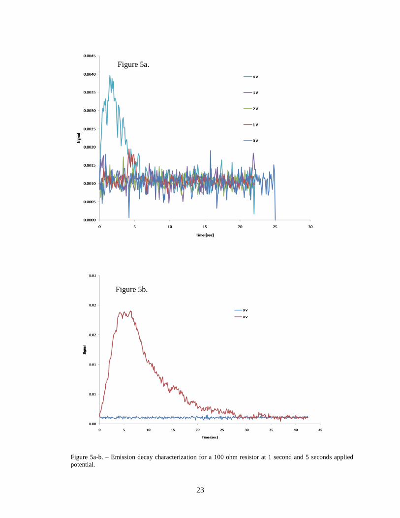
Radiation Decay Characterization As seen in Figures 5 and 6, for both 1 second (part a on each figure) and 5 seconds (part b on each figure) applied potentials, it can be seen that the pyrolized Kapton emitted more radiation than the resistor. Further studies need to be completed using a wider range of time differentials and applied potentials, such as a short (0.10 second), high potential (10 Volts) application.
23
Figure 5a-b. – Emission decay characterization for a 100 ohm resistor at 1 second and 5 seconds applied potential.
Figure 5b.
Figure 5a.

24
Figure 6a-b. Emission decay characterization for a 100 ohm Kapton filament at 1 second and 5 seconds applied potential.
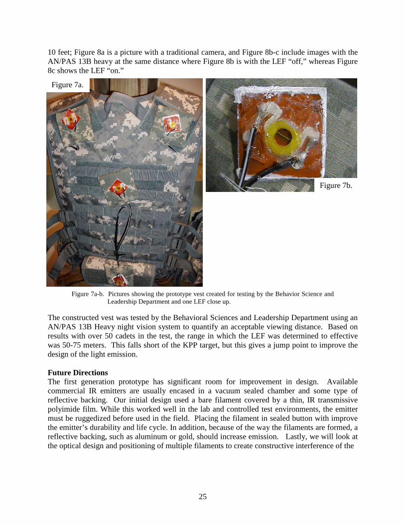
Building and Testing of an IFF device Figure 7a-b shows a picture of the prototype vest that was constructed. One can see 4 LEFs wired to the controller board at the bottom of the vest. Figure 7b shows the feasibility to keep the design of the LEF basic, and make the device relatively rugged based even thought the construction used extremely simple and inexpensive components. Figure 8a-c shows a picture of a CDT Eric Creighton wearing the vest with one functioning LEF at a distance of approximately
Figure 6a.
Figure 6b.
25
10 feet; Figure 8a is a picture with a traditional camera, and Figure 8b-c include images with the AN/PAS 13B heavy at the same distance where Figure 8b is with the LEF “off,” whereas Figure 8c shows the LEF “on.”
Figure 7a-b. Pictures showing the prototype vest created for testing by the Behavior Science and Leadership Department and one LEF close up.
The constructed vest was tested by the Behavioral Sciences and Leadership Department using an AN/PAS 13B Heavy night vision system to quantify an acceptable viewing distance. Based on results with over 50 cadets in the test, the range in which the LEF was determined to effective was 50-75 meters. This falls short of the KPP target, but this gives a jump point to improve the design of the light emission. Future Directions The first generation prototype has significant room for improvement in design. Available commercial IR emitters are usually encased in a vacuum sealed chamber and some type of reflective backing. Our initial design used a bare filament covered by a thin, IR transmissive polyimide film. While this worked well in the lab and controlled test environments, the emitter must be ruggedized before used in the field. Placing the filament in sealed button with improve the emitter’s durability and life cycle. In addition, because of the way the filaments are formed, a reflective backing, such as aluminum or gold, should increase emission. Lastly, we will look at the optical design and positioning of multiple filaments to create constructive interference of the
Figure 7a.
Figure 7b.

26
Figure 8a-c. Pictures showing CDT Eric Creighton wearing the LEF vest (Figure 8a), one LEF “off” (Figure 8b), and the LEF “on” (Figure 8c).
emission sources. Dependent on the number of filaments per individual light emitter, the intensity should increase significantly, although battery lifetime will probably decrease. The second area for improvement is in filament optimization. The unique, sponge-like structure and glassy carbon/graphite composition of the laser carbonized filaments allow for potential modification using a variety of chemical reactions. Graphite and glassy carbon can be intercalated with several different compounds. The filaments can be surfaced doped post laser pyrolysis or the polyimide can be pretreated with coatings to form new pyrolisis products within the filament. Plans include testing using oxidation/reduction intercalation reaction with sulfuric
Figure 8b.
Figure 8c.
Figure 8a.

27
acid mixtures for doping post pyrolysis and using pretreated polyimide film with nitronium and boron salts. In regards to pretreatment, a visit to George Whitesides’ lab at Harvard gave us some insight on how to deposit these compounds on the surface inexpensively.(9,10) These potential chemical changes might allow us to narrow the response range of the filament and increase its emission. In addition to chemical means, the electrical properties of the filament can be adjusted by varying the laser pyrolization energy. While this is easily done in the lab, we have not had the resources to fully explore the wide range of configuration options. Filament optimization will be probably be addressed, with input laser pyrolisis variables such as focus length, laser power, scan speed, and wavelength the main focus of the study. Cadet and Faculty Involvement LTC John M. Ingram (PI) Dr. Thomas M. Spudich (new PI) LTC Gregory R. Kilby CDT Bryan Bird CDT Eric Creighton CDT Katie Fenton CDT Jesse Teahon CDT Jenn Vanecek CDT Claire Heid CDT Blake Rulison CDT Kyle Johnson Acknowledgements Funding from the Army Research Labs and Program Executive Officer Soldier supported this research. We would like to thank DuPont for generously donating the Kapton. References
1. Hall RR, Wilson WD, Loehle WD, Allbee DC. Formation of a porous, patternable, electrically conducting carbon network by the ultraviolet laser irradiation of the polyimide PMDA-ODA (Kapton). Chemistry of Materials 1994;6:888.
2. Srinivasan R, Hall RR, Wilson WD, Loehle WD, Allbee DC. Ultraviolet laser irradiation of the polyimide, PMDA-ODA (KaptonTM), to yield a patternable, porous, electrically conducting carbon network. Synth.Met. 1994;66:301.
3. Srinivasan R, Hall RR, Loehle WD, Wilson WD, Allbee DC. Chemical transformations of the polyimide Kapton brought about by ultraviolet laser radiation. J.Appl.Phys. 1995;78(8):4881.
4. Wynn GH, Fountain AWI. Development and characterization of electrochemical devices using ultraviolet laser induced carbonization of polyimide films. J.Electrochem.Soc. 1997;144(11):3769.

28
5. Dinetz SF, Bird EJ, Wagner RL, Fountain III AW. Thermal and UV laser pyrolysis of the polyimide PMDA-ODA: analysis of the gaseous products by time-resolved and discrete infrared spectroscopy. : Brill Academic Publishers; 2001. p. 55.
6. Dinetz SF, Bird EJ, Wagner RL, Fountain III AW. A comparative study of the gaseous products generated by thermal and ultra-violet laser pyrolyses of the polyimide PMDA-ODA. Journal of Analytical and Applied Pyrolysis 2002;63:241.
7. Ingram JM, Greb M, Nicholson JA, Fountain III AW. Polymeric humidity sensor based on laser carbonized polyimide substrate. Sensors and Actuators B 2003;96:283.
8. Ingram JM, Nicholson JA, Fountain III AW. Development and optimization of a laser carbonized polyimide film as a sensor substrate for an all-polymer humidity sensor. In: Mittal KL, editor. Polyimides and Other High Temperature Polymers, Volume 2 The Netherlands: Brill Academic Publishers; 2003. p. 437.
9. Gates BD, Xu Q, Stewart M, Ryan D, Willson CG, Whitesides GM. New Approaches to Nanofabrication: Molding, Printing, and Other Techniques. Chem.Rev. 2005;105:1171-1196.
10. Deng T, Wu H, Brittain ST, Whitesides GM. Prototyping of Masks, Masters, and Stamps/Molds for Soft Lithography Using an Office Printer and Photographic Reduction. Anal.Chem. 2000;72:3176-3180.

29
Department of Electrical Engineering & Computer Sciences

30
VLSI Electronics for Photonic Image Processing, Smart Pixel Technology and Optical A/D Conversion
COL Robert W. Sadowski and COL Barry L. Shoop
Photonics Research Center
Department of Electrical Engineering and Computer Science US Military Academy, West Point NY 10996 USA
e-mail: robert.sadowski or barry.shoop @usma.edu Abstract. We report on improvements to an underlying hardware approach to implement a neural network for real-time image halftoning. We present theoretical and experimental results using a modified current starved comparator as the quantizing element. The neuron is self-biasing with error weighting achieved through current division to enable operation at a variety of bias voltages. The circuit is designed for eventual integration with a photodiode array for imaging applications.
Background Digital halftoning is a technique originally developed for grayscale print and display applications but has progressed to color and multispectral applications. In the case of grayscale images, halftoning is a process for converting continuous tone images into binary valued images. The human visual system perceives the illusion of a continuous tone even though only black and white values are used to render the image. An optoelectronic implementation of the error diffusion neural network (EDN) uses a photodiode array integrated with an underlying electronic neural network for halftone computation. EDNs spatially distribute the quantitization error across an image through weighted interconnects to reduce correlated artifacts and perform spectral noise shaping. Our approach to the error diffusion neural network provides the ability to perform real-time image halftoning for applications such as remote sensing, xerography, and facsimile enabling digitization in a single step. This report describes specific improvements in the design and performance of the silicon circuitry.
Theory Halftoning Theory One of the most popular halftoning processes, originally introduced by Floyd and Steinberg[1], uses an error diffusion algorithm in which each individual pixel value is quantized and the resulting quantization error is diffused in a predetermined weighted pattern to neighboring pixels. The distributed error influences the quantization decision of the neighboring pixels in order to improve the overall quality of the halftoned image.
A variety of error diffusion algorithms have been proposed which differ in their diffusion pattern [Jarvis, Stucki]. In conventional unidirectional error diffusion, the algorithm raster scans the image (typically from upper left to lower right) and the quantization error from each pixel is diffused forward and down in a fixed, deterministic weighted pattern. For each pixel, a binary quantization decision is made based on the intensity of the individual pixel and the weighted error diffused from the previously quantized pixels. As a result of this unidirectional processing,

31
the diffusion filter is necessarily casual and results in undesirable visual artifacts that are not part of the original image but instead result from the algorithm. Several of these correlated visual artifacts are identified by the arrows in the halftoned image in Figure 1. We have developed a two-dimensional error diffusion algorithm that improves overall halftone image quality [2,3]. In this implementation, all quantization decisions are made in parallel and the error is diffused symmetrically in two spatial dimensions. Visual artifacts previously attributable to the unidirectional halftoning algorithm are eliminated and the overall halftoned image quality is improved as depicted in Figure 2.
Computer simulations of the two-dimensional error diffusion neural network have produced some of the best halftoned images to date. However, software implementation is generally not practical due to the computational complexity of the algorithm. The neural algorithm is ideally suited for implementation in analog circuitry.
Fig. 1. Visual artifacts from halftoning process. The image on the left is the original gray scale. The image on the right has been halftoned using the Floyd-Steinberg algorithm. Note the visual artifacts seen near the arrows.
Fig. 2. Reduced visual artifacts from the halftoning process. The image on the left is the original gray scale. The image on the right has been halftoned using the Shoop-Ressler algorithm. Note the reduction in visual artifacts as compared to Figure 1.
Previous work We have previously explored several smart pixel technologies as possible hardware implementations to achieve real-time function of the neural halftoning algorithm.[4] Proof-of-concept smart pixel arrays (SPAs), using different approaches were manufactured and tested to evaluate their capability to implement the full-scale error diffusion neural network: flip-chip bonding of gallium arsenide (GaAs) self electro optic effect device (SEED) modulators on silicon CMOS circuitry [5,6]; liquid crystal spatial light modulators integrated with silicon CMOS circuitry, referred to as liquid crystal on silicon (LCOS) [7]; and monolithic integration of LEDs with GaAs circuitry using Epitaxy-on-Electronics (EoE) [4,8]. All have demonstrated promise as viable technologies capable of high quality halftoned images at video frame rates. These proofs of concept circuits consumed too much power for large scale integration.

32
Previously we designed a scalable neuron architecture that meets reduced current requirements for practical array sizes. The following sections describe the basic theory, neural circuitry, and design methodology. Our target process is 0.35 µm with NIR photodiode array integration for limited visibility sensing.
Fig. 3. Basic EDN neuron. All state variables are currents. A single pixel on the photodiode array generates an input current of x(r,c).
Error Diffusion Network Functionality Basic Neuron Figure 3 depicts the block diagram of a single EDN pixel. The theoretical analysis underpinning the EDN is described elsewhere [2,3]. The circuitry to implement a single neuron of the neural network consists of a one-bit quantizer with finite slope, two summing nodes, and error weighting for the diffusion filter. The error weighting scheme comprises the largest physical portion of the design. State variables are represented as currents which lends itself to photodiode array implementation. The input optical input image generates analog photocurrents corresponding to individual pixel intensities. The input current at a particular row (r) and column (c) is represented by x(r,c). Error currents from adjacent neurons are subtracted creating the state variable u(r,c) which is then passed to the quantizer. The quantizer provides a smooth thresholding function for the neuron producing the output signal y(r,c). The output signal is compared to the original state variable u(r,c). The difference between the original quantizer input u(r,c) and the output y(r,c) is the total error current ε(r,c). This error current is spatially distributed to adjacent neurons according to a weighted 2-D error diffusion filter shown in Figure 4. The error diffusion filter is circularly symmetric with the coefficient weights inversely proportional to the radial distance from the neuron.
Fig. 4. 2-D Error diffusion filter. The central dot represents an individual neuron. The numbers represent the desired error current fraction diffused to nearby neurons. The labels in parentheses were used during simulation.

33
The neuron-to-neuron interconnections are accomplished using CMOS metallization layers. Our original work relied upon a Carver Mead-based quantizer using a wide-range transconductance amplifier. Each neuron comprised 90 transistors, but consumed nearly 2 mA per pixel in 0.5 µm technology making it unrealistic for large-scale integration.
Design Methodology Although an analog current based device, we use standard digital CMOS fabrication runs available through MOSIS. Accurate analog simulations normally require SPICE models that include small geometry and subthreshold effects. Unfortunately MOSIS provided extracted run parameters represent an average set of extractions optimized for a digital audience. We analyzed extracted run parameter sets and opted for larger transistors than normally required for digital circuits to minimize mismatch effects. We began our efforts using 5V 1.5 µm silicon (AMIS ABN) because lower fabrication costs allow us to iterate prior to going to smaller feature sizes. We verified circuit operation and experimental procedures in the 1.5 µm process and have moved 0.5 µm AMIS C5F. We currently have designs in fabrication in 3.3V 0.35 µm TSMC. Smaller feature sizes offer area savings and achieve packing densities required to create large image sizes.
Current starved Comparator based neuron Desired Neuron Characteristics The 2-D EDN theory places several constraints on the circuit implementation. The quantizer must be symmetric about zero input current with quantized current output that is positive or negative. A quantizer transition slope of approximately thirty produces the best images. Error currents are linear scaled percentages that are bi-directional with allowable tolerances on the order of ten percent and desired weights of 11.24%, 7.45%, 2.45% and 1.81%. Small current values must be accurately summed and passed to neighboring elements. The network convergence time must be quick enough to allow video frame rates. The analog circuit must tolerate run-to-run parameter variations. A photodiode offset equal to half of the quantizer range must be subtracted from each pixel compensating for the positive only input photocurrent. Finally, we desire the circuit to work with different bias voltages enabling a rudimentary gain control for low light conditions. The circuitry shown in Figure 5 implements all of these features and depicts the core of the neuron: a one-bit quantizer with finite slope and two summing nodes. Lower bias voltages produce a quantized output for a lower input current level, i.e. gain control.
Summing Nodes Summing elements are constructed using cascoded inverter pairs with diode connected inputs (see the first set of 8 transistors in Figure 5). These modified inverter pairs form a unity-gain push/pull current amplifier with low input impedance, high output impedance, reduced bias current, and cutoff exceeding several MHz. The stage has a nominal current gain of minus one. The nodes linearly transfer current with inputs exceeding +/- twice the DC bias current per stack.
Quantizer The quantizer is a modified current starved comparator often found in VCO circuits. A reference current is generated by a four diode-connected transistor stack similar to the summing node input. To achieve of slope near thirty, two cascoded outputs serve as high impedance loads reducing the sharp quantizer transition. The quantizer itself generates an output centered about

34
zero input current. The output is monitored by a parallel comparator driving an open drain NMOS transistor. A third quantizer with input tied to VDD generates a photodiode offset current fed to the first summing node.
Fig. 5. Basic neuron circuit without the error weight circuitry. State variables are represented by analog currents.
Fig. 6. Diffusion error weight circuitry for the four error weights. The first three weights have four outputs each labeled A-D. Error weight 4 has eight outputs labeled A-H. The circuit scales the error current ε(r,c) by 11.11%, 7.41%, 2.47%, and 1.85% respectively.
Error Weights The error weight circuitry is depicted in Figure 6. Originally we tried W/L scaling to generate the error currents. However, DC offsets exceeding the error currents were generated as a result of the non-identical transistors being tied to summing node inputs. To avoid the systematic offsets we employed a fractional current division approach. Random process mismatches will generate offsets that should average out across an entire array of devices. By loading a high impedance summing node output with nine low impedance diode connected stacks, we generate an error current that is one ninth or 11.11% of the original current in a single stack. The mirrored current

35
lies within five percent of the 11.45% desired value. We generate the second weight by tying two high impedance outputs into three low impedance loads and mirroring the result (7.41% is roughly two thirds of 11.11%). The remaining weights are realized in a likewise fashion. The weights are then spatially fed to adjacent neurons as shown in Figure 4. Although the entire neuron contains 256 transistors, we can build the entire circuit from only one set of matched PMOS/NMOS transistors. The tradeoff for the self-biasing diode connected transistor stacks is reduced power supply noise immunity. However, the target application is battery powered and the ability to retain functionality at lower supply voltages coupled with scalability makes this an attractive approach.
(a) (b) Fig. 7. (a) Simulated neuron response vs. input photocurrent. The quantizer output current is scaled by one quarter. (b) Simulated error weights with linear fits.
Comparison of Error 1 thru 4
-0.02
-0.01
-0.01
0.00
0.01
0.01
0.02
0.00 0.50 1.00 1.50 2.00 2.50
Input Current in uA
Erro
r Wei
ght O
ut (
Arb
. Uni
ts)
VE_In - B_E1A
VE_In - B_E2A
VE_In - B_E3A
VE_In - B_E4A
(a) (b)
Fig. 8. (a) Measured comparison of four duplicate Error 1 weights. (b) Comparison of four different error weights from single device. Results from MOSIS T63Y run.
Early Simulation and Measured Results Our experimental setup consisted of a PC running ICCAP and an Agilent 4156C Semiconductor Parameter Analyzer. The simulations did not include any bonding parasitics. Figures 7 and 8 depict comparisons between predicted and measured performance in PSPICE using extracted BSIM 3.3.1 MOSIS T58B run parameters. The simulated quantizer output in Figure 7 has been reduced by four to emphasize the error weights. Figure 8 shows measured error weight performance for a single neuron design in the 1.5 µm silicon. We conducted a series of swept measurements to confirm neuron operation. Figure 8 shows results from the error weight
Error Weight 1 Comparison
-0.015
-0.010
-0.005
0.000
0.005
0.010
0.015
0.00 0.50 1.00 1.50 2.00 2.50Input Current in uA
Erro
r Wei
ght O
ut (A
rb U
nits
)
VE_In - B_E1A
VE_In - B_E1B
VE_In - B_E1C
VE_In - B_E1D

36
measurements. It is difficult to measure the actual current flowing through the error weights. However, by measuring the voltage we can approximate the current flow between nodes. We measured the same error weight and determined that the variation (n=20) was less than 2% between individual weights of the same size. We then determined the ratio of the error weights to each other to confirm our ratio metric approach to designing the error weights. The expected values is in parentheses for a sample size of n=4: Error Weight 1 - 11.10% Measured (11.11% expected), Ratio of Error Weight 1 to 2 - 66.5% Measured (67% Expected), Ratio of Error Weight 2 to 3 - 33.7% Measured (33% Expected), and Ratio of Error Weight 2 to 4 ~ 25.3% Measured (25% Expected).
Expanding beyond single neurons, simulated halftones for larger neural arrays produced results in concert with theory. We were software limited to 32 x 32 arrays containing 1,024 pixels comprising over 250 thousand transistors. Figure 9 depicts the one-quarter, one-half, and three-quarter grayscales for the T24P parameter set. Our goal is to reproduce these results in silicon before integrating any photodiode array.
Fig. 9. Simulated output for a 32 x 32 array for (a) one-quarter, (b) one-half, (c) and three-quarter grayscale inputs.
Chip Layouts Figure 10 shows the complete chip layout, blow-up of the central neuron with locations of the key elements, and a micrograph of the finished device.
Fig. 10. (a) Chip layout for three neurons including HiESD pad circuitry with (b) single neuron and (c) micrograph of fabricated central neuron on AMIS ABN run T58B via MOSIS.
Although the results were promising as a proof of concept, the layout had several challenges: a

37
high-aspect ratio and non-standard transistor layout with active cuts made individually. We undertook considerable effort to reduce and symmetrize the neuron footprint while retaining circuit performance. This required restarting the layout from scratch. We decided to complete these efforts before scaling to smaller feature sizes. Figure 11 depicts some of the neuron changes implemented in the 1.5 µm silicon as part of the optimization. We achieved a roughly twenty percent decrease in area without altering the circuit design. Active cuts now contained multiple transistors and sub-circuits were stacked horizontally rather than vertically. Figure 11 shows the revised central neuron with locations of the key elements with a micrograph of a finished device in Figure 12.
(a)
(b) Fig. 10. Chip layout for the (a) original single neuron and (b) the revised central neuron. The active cuts are depicted in lime green and occur in a multi-transistor trench in (b) as opposed to individually in (a). A higher packing density can be achieved in the revised layout resulting in ~20% less area required.
Quantizer
Error 4
Error 2 & 3
Error 1

38
Fig. 11. Chip layout for a 6x6 array with the revised central neuron and a micrograph of a fabricated central neuron on an AMIS 1.5 µm silicon through MOSIS ABN run via MOSIS.
Scaling to smaller feature sizes Currently we have two designs in fabrication in both 05. µm and 0.35 µm technologies. They are essentially the same design and depicted in Figure 12. These designs were created by simply scaling to smaller feature sizes while maintaining the original NMOS/PMOS aspect ratios. Once we verify individual neural operation (response symmetry and appropriate error weighting), we will construct fully interconnected diffusion networks for electrical testing. In a parallel effort, we will layout lateral diodes to explore potentially combining these on a single device for photodiode inputs rather than flip-chip bonding .
(a) (b)
Fig. 12. Chip layouts for a 7x7 arrays with the revised central neuron in (a) AMIS 0.5 µm and (b) TSMC 0.35 µm silicon through MOSIS that are currently in fabrication. The layout has been shrunk to fit in the same vertical dimension. The outer pads are actually the same size: 80 x 80 µm.

39
Future Direction We are confident that we have identified a circuit topology and technical approach to real-time halftoning. We will continue the development of smart pixel technology in an effort to demonstrate a hardware platform capable of providing real-time processing for the error diffusion neural algorithm. This solution allows implementation of the entire neuron utilizing a single pair of matched NMOS/PMOS transistors. Our next step is to validate performance as we migrate from 0.5 to 0.35 µm devices. We expect to expand our new design to larger interconnected array sizes. Current place and route routines have difficulty creating the symmetrical interconnects required for our meshed architecture. Our target architecture, a 32 x 32 array will have 24,000 neural interconnects. We can easily expand the design as was done in earlier implementations, but with huge sacrifices of layout space where seventy percent of the design was dedicated to interconnects. We are optimizing our interconnect scheme while the latest devices are in fabrication by exploring geometric arrangements that should enable more compact interconnection using the upper metal layers. Cadet and Faculty Publications Faculty:
P. Patterson, PhD. Dissertation. George Washington University, May 2009.
P. Patterson, R. Polcawich, and J. Zara, " Polyimide as a Structural Material in Piezoelectrically Actuated Microelectromechanical Systems," The 15th Annual Army Research Laboratory/United States Military Academy Technical Symposium, Atlantic City, NJ, October 30-31, 2007.
P. E. Patterson, J. M. Zara, "Real-time high-displacement amplified bimorph scanning mirror", Proceedings of the SPIE, Optomechatronic Actuators, Manipulation, and Systems Control. volume 6374, Boston, MA. 63740B, 2006.
P. E. Patterson, M. Dubey, J. Pulskamp, R. Polcawich, L. Currano, and J. Zara, "Piezoelectric polyimide scanning micromirror" Proceedings of The 14th Annual Army Research Laboratory/United States Military Academy Technical Symposium, November 2006.
R.W. Sadowski, M. C. Ballmann, and B.L. Shoop, “A Neural Network CMOS Circuit Implementation for Real-Time Halftoning Applications,” Proceedings of the 49th International IEEE MW Circuits and Systems Symposium, Image Processing II, C2L-E, IEEE, Aug 2006.
R.W. Sadowski and B.L. Shoop, “Error Diffusion Neural Network Implementation for Real Time Halftoning Applications,” Frontiers in Optics: The 89th OSA Annual Meeting, FWO3, Optical Society of America, Oct 2005.
Student:
M. C. Ballmann and R.W. Sadowski, “Experimental Validation of a CMOS Circuit Implementation for Real-Time Halftoning Applications Using an Error Diffusion Neural Network,” Proceedings of the National Conference of Undergraduate Education, April 2007.

40
Cadet Design Project Teams:
2006: Optical Parking Assistant: CDT Ivan Knez, CDT Nediljko Radanovic, and CDT Juan Ramos.
References [1] R. Floyd and L. Steinberg, "An adaptive algorithm for spatial gray scale," Society for Information Display
Digest, vol. 75, pp. 35-36, 1975. [2] B. L. Shoop and E. K. Ressler, "An error diffusion neural network for digital image halftoning," Proc. IEEE
Workshop on Neural Networks, Boston, Massachusetts, pp. 427-436, 1995. [3] E. K. Ressler and B. L. Shoop, "High quality digital halftones from error diffusion networks," Proc. Society for
Information Display, San Diego, California, pp. 506-509, 1996. [4] D. A. Hall, B. L. Shoop, J. R. Loy, G. B. Tait, E. K. Ressler, J. F. Ahadian and C. G. Fonstad, “Performance of
GaAs smart pixel components before and after monolithic integration of InGaP LEDs using Epitaxy-on-Electronics technology,” Optics Express, vol.4, no. 4, 1999.
[5] B. L. Shoop, A. H. Sayles, D. A. Hall and E. K. Ressler, "A smart pixel implementation of an error diffusion neural network for digital halftoning," Special Issue of International Journal of Optoelectronics on Smart Pixels (Invited), vol. 11, pp. 217-228, 1997.
[6] D. A. Hall, A. H. Sayles, G. P. Dudevoir, R. W. Sadowski and B.L. Shoop, "Experimental demonstration of a 5x5 smart pixel neural array for digital image halftoning," OSA Annual Meeting Technical Digest (Postdeadline), Washington, D.C., 1998.
[7] D. A. Hall, B. L. Shoop, G. P. Dudevoir and A. H. Sayles, "Experimental demonstration of a 3x3 liquid crystal on silicon smart pixel array for digital image halftoning," OSA Annual Meeting Technical Digest, Washington, D.C., 1998.
[8] D. A. Hall, B. L. Shoop, J. R. Loy, G. B. Tait, E. K. Ressler, J. F. Ahadian and C. G. Fonstad, Jr.,"Experimental demonstration of a 3x3 monolithically integrated smart pixel array based on Epitaxy-on- Electronics,” OSA Annual Meeting Technical Digest (Postdeadline), Washington, D.C., 1997.
41
Minimization of color halftone texture visibility using three-dimensional error diffusion neural network
Dr. Wenli Huang, COL Eugene Ressler, COL Barry Shoop and Dr. Jean Blair
Photonics Research Center
Department of Electrical Engineering and Computer Science United States Military Academy, West Point, NY 10996
e-mail: [email protected] Abstract. Previously we have shown that error diffusion neural networks (EDNs) find local minima of frequency-weighted error between a binary halftone output and corresponding smoothly varying input, an ideal framework for solving halftone problems. An extension of our work to color halftoning employs a three dimensional (3D) interconnect scheme. We cast color halftoning as four related sub-problems: the first three are to compute good binary halftones for each primary color and the fourth is to simultaneously minimize frequency-weighted error in the luminosity of the composite result. We have showed that an EDN with a 3D interconnect scheme can solve all four problems in parallel. This paper shows that our 3D EDN algorithm not only shapes the error to frequencies to which the Human Visual System (HVS) is least sensitive but also shapes the error in colors to which the HVS is least sensitive. The correlation among the color planes by luminosity reduces the formation of high contrast pixels, such as black and white pixels that often constitute color noise, resulting in a smoother and more homogeneous appearance in a halftone image and a closer resemblance to the continuous tone image. The texture visibility of color halftone patterns is evaluated in two ways: (1) by computing the radially averaged power spectrum (2) by computing the visual cost function. Introduction Color halftoning is a process by which a continuous-tone image is rendered using only binary valued pixels in the three primary color planes. Error diffusion is one method of halftoning in which the error associated with a nonlinear quantization process is diffused within a local region and subsequent filtering methods are employed to improve some performance metric. The goal is to create an image that the human eye perceives as a continuous tone image due to the limited spatial frequency response and color sensitivity of the HVS. A classic error diffusion algorithm, such as first introduced by Floyd and Steinberg1, raster scans the image and performs the quantization and error distribution pixel by pixel in a particular direction. The one-dimensional filter, also called scale error diffusion, often leads to undesirable visual artifacts. We have previously developed a two-dimensional (2D) monochromatic halftoning approach using an EDN that diffuses the error symmetrically in all directions in the image plane2,3,4. The advantage of the neural algorithm is that all pixel quantization decisions are computed in parallel and therefore the error diffusion process becomes un-directional and symmetric. This had eliminated the artifacts caused by the scalar error diffusion. One approach of color halftoning is to halftone each color plane independently using identical error diffusion filters. This often yields color artifacts and poor color rendition because it does not exploit correlations among the color planes. A common visual effect is the halftone texture formed by high contrast adjacent pixels. Such brightness variation among adjacent pixels is a major cause of color noise. Better color halftone quality can be obtained by limiting the number of output colors in a local region. Many methods have been studied to constrain the primary colors so to avoid overlapping dots wherever possible to reduce the visibility of halftone texture and generate the smoothest possible halftone pattern5,6. An extension of our previous work to color images employs a new three-dimensional interconnection scheme by adding a luminosity

42
error filter as the 3rd dimension7. We claim that to produce color halftones with minimum halftone texture visibility, an EDN must perform four tasks simultaneously: minimize frequency-weighted error between (1) red outputs and inputs, (2) green outputs and inputs, (3) blue outputs and inputs, and (4) luminosity of the output and luminosity of the input. We have designed a 3D EDN filter that performs the above four tasks in parallel with user-adjustable emphasis on the relative importance of weighted error in luminosity. The algorithm provides synchronization of the red, green and blue halftone solutions so that luminosity error is shaped concurrently with error in each of the primaries. Finally, the texture visibility of our color halftone patterns is evaluated and compared with Floyd-Steinberg’s halftoning methods by using Ulichney and Lau’s method8,9 to compute the radially averaged power spectrum in luminosity errors and by using the visual cost function introduced by Sullivan10. Three Dimensional Error Diffusion Neural Network Artificial neural networks are groups of interconnected processing elements called “neurons” working in parallel to achieve a specific task. The interconnect strengths between neural pairs are called “weights”. Each neuron receives inputs from other neurons that are interconnected to it and sums them to produce an output through a nonlinear transfer function. The output in turn passes to other neurons through the interconnect weights. Neural networks are naturally applicable in solving optimization problems. Specifically, the problem of creating a halftone image can be cast in terms of an optimization problem where the performance metric to be minimized is the difference between the original and the halftone images. The pixels on which error diffusion and quantization are performed resemble the neurons. The interconnect weights of the error diffusion filter resemble the strengths between the neural pairs. Since introduction of error in the halftoning process is inevitable, this energy-minimizing behavior of the network is ideal in the sense that it allows output error to be “shaped” toward frequencies outside the signal band.
We are concerned with analyzing error diffusion algorithms for computing good halftones. A halftone algorithm is a function, y=h(x), where x is a discretely sampled real-valued input. Values of x are drawn from [0,1]. The corresponding binary output, y, is drawn from {0,1}. By convention, zero is black and one is “as bright as possible'' for the output device. A halftone algorithm is considered good if it produces good halftones. As11, we consider function E(x,y) defined as the sum of squares of spatial frequency-weighted error between x and y and a low value of E is equivalent to a good halftone. Thus the algorithm that achieves minimum E for
Figure 1. Block diagram of an error diffusion architecture.

43
given x is optimal. Figure 1 shows the block diagram of an error diffusion network. In equilibrium, the error diffusion neural network satisfies
xuyWu +−= )( (1) which results in an equivalence to the Hopfield network. Hopfield showed12 that when the matrix of interconnect weights W is symmetric with zero diagonal elements and the high-gain limit of the sigmoid ℑ[·] is used, the stable states of the outputs are the local minima of an energy function. It cab be proven that EDN converges to a local minimum of the energy function7
AeexyAxy
AxxAxyAyyyxET
error
T
error
TTT
=−−=
+−=
)()(
2),(, where 1)( −+= WIA (2)
The Fourier transform of this convolution yields a useful alternative form of Equation (2)
21
0
21
0)~(~)~~(~),(~
kk
n
kkk
k
n
keAxyAyxE ∑=−∑=
−
=
−
= (3)
Equation (3) shows that EDNs offer a natural tool for digital halftoning subject to a frequency-weighted square error. Behavior of the network is determined by the N ×N matrix of weights W, which filters the errors. Filtered errors are fed back to neuron inputs through a vector sum element which adds to the input gray image x.
An EDN for color halftoning has, in our case, three neurons per pixel, one for each primary color. We assume these are red, green, and blue. Hence the color of an input pixel is completely described by a triple <xR, xG, xB> ∈ [0,1]3, and an output pixel by <yR, yG, yB> ∈ {0,1}3. Output pixels thus have one of eight possible colors including black and white. Figure 2 illustrates our three-dimensional error diffusion scheme. The arrows indicate the directions in which error diffuses. We choose 7×7 matrices as the error diffusion weights, W. Consider a green pixel in the center of a 7×7 color pixel array. The quantization error from the green pixel diffuses symmetrically in three dimensions as follows: The error is distributed by weights WGG to its 48 neighbor green pixels; the error is also distributed to its 49 neighbors in the red plane by interconnect weights WGR and to its 49 neighbors in the blue plane by interconnect weights WGB. The same scenario applies to red and blue pixels.
RGB RGB (Original)
(Halftoned)
WRR
WGG
WBB
WRG=WGR
WGB=WBG
WRB=WBR
Figure 2. Three-dimensional EDN

44
The in-plane error diffusion weights, WRR, WGG and WBB, can each be taken as the ones we previously found in monochromic halftoning2,4,
===
0.0005 0.0020 0.0052 0.0069 0.0052 0.0020 0.0005 0.0020 0.0104 0.0249 0.0329 0.0249 0.0104 0.0020 0.0052 0.0249 0.0584 0.0767 0.0584 0.0249 0.0052 0.0069 0.0329 0.0767 0 0.0767 0.0329 0.0069 0.0052 0.0249 0.0584 0.0767 0.0584 0.0249 0.0052 0.0020 0.0104 0.0249 0.0329 0.0249 0.0104 0.0020 0.0005 0.0020 0.0052 0.0069 0.0052 0.0020 0.0005
BBGGRR RWW (4)
The sum of the weights is 1 so that the error is not amplified or reduced and the total intensity is kept the same for each primary color. The cross-plane weights, WRG, WRB and WGB, the 3rd error diffusion dimension, must maintain the advantage of being non-directional and symmetric. The sum of the weights must be zero so that there is no net transfer of color from one primary to the others. Such filters are constructed based on minimizing the luminosity error. The luminosity of an arbitrary pixel <r, g, b> is
.1 and 0,, where, RR =++>++= BGBGBGR bgrl βββββββββ (5) The constant βR, βG, and βB correspond to the relative visual sensitivity of the human eye to the primaries. Standard values are
.11.0 and ,59.0 ,30.0R === BG βββ (6) We claim that to produce good color halftones, an EDN must perform four tasks simultaneously:
• Minimize frequency weighted error between red outputs and inputs, and the same for green and blue.
• Minimize frequency-weighted error between luminosity of the output and luminosity of the input.
The importance of the first three tasks is clear. They can be performed by three separate EDNs working independently. The last is more subtle and best illustrated by examples. Suppose four pixels with identical 25% gray values, < 0.25, 0.25, 0.25 >, are halftoned. To minimize 0 Hz error, the EDN must fill one (otherwise black) pixel with each of red, green, and blue. There are many ways to do this. One way is to fill all red, green and red on one pixel (resulting a white pixel), and leave the other three pixels black. Another way is to fill red, green and red on three different pixels and leave one pixel black. All these results are equally likely if the red, green, and blue outputs are computed independently. Yet they are far from equal in quality with respect to luminosity error. Clearly some methods of combining red, green, and blue primaries are better than others. Hence the introduction of the 3rd dimension in error diffusion serves as a constraint to the halftone fill-in patterns from the three primaries. Weights WRG, WRB and WGB are directed at “synchronizing” the red, green, and blue halftone solutions so that luminosity error is shaped concurrently with error in each of the primaries. The detailed theoretical treatment of finding such filters is presented in our published work7. If we consider the color halftoning EDN to be organized as three “planes” of neurons — red, green, and blue — then the interconnection weights of neurons within any plane are identical to W for monochrome halftones. We can use the same convolution kernel as shown in our earlier work in Equation 4.

45
Connections between the red and green planes are kRG(W + I). The corresponding convolution kernel is obtained by replacing the center zero of the monochrome kernel with a one and multiplying the whole by kRG = kGR, where
GRGRRG d
bkkββ
−==
1 and BR
BRRB dgkkββ
−==
1 , BG
BGGB drkkββ
−==
1 (7)
Here
21 and ,21 ,21B
BbG
GgR
Rrβ
ρ
β
ρ
β
ρ+=+=+= (8)
where ρR, ρG, ρB > 0 is user adjustable with a constraint
drgrbgb
BBR=
−=
−=
−222
111βββ
(9)
Here, d is an arbitrary positive value. ρR, ρG, ρB set the importance of primary color errors relative to luminance. Note that the resulting kernel sums to zero. Thus error in one plane influences only the phase of patterns in the others, not their mean values. Red-blue and green-blue interconnections are similar, using kRB and kGB respectively. For example, choose ρR = 2; errors in the red color plane have two times the weight of luminosity errors in the minimization performed by the EDN. Then we find ρG = 1.7, ρB = 2.0, kRG = -.0842, kRB = -.0133, and kGB = -0.0299. The resulting cross plane interconnection weights are:
−==
0.0000- 0.0002- 0.0004- 0.0006- 0.0004- 0.0002- 0.0000-
0.0002- 0.0009- 0.0021- 0.0028- 0.0021- 0.0009- 0.0002-
0.0004- 0.0021- 0.0049- 0.0065- 0.0049- 0.0021- 0.0004-
0.0006- 0.0028- 0.0065- 0.0842 0.0065- 0.0028- 0.0006-
0.0004- 0.0021- 0.0049- 0.0065- 0.0049- 0.0021- 0.0004-
0.0002- 0.0009- 0.0021- 0.0028- 0.0021- 0.0009- 0.0002-
0.0000- 0.0002- 0.0004- 0.0006- 0.0004- 0.0002- 0.0000 -
GRRG WW (10)
−==
0.0000- 0.0000- 0.0001- 0.0001- 0.0001- 0.0000- 0.0000-
0.0000- 0.0001- 0.0003- 0.0004- 0.0003- 0.0001- 0.0000-
0.0001- 0.0003- 0.0008- 0.0010- 0.0008- 0.0003- 0.0001-
0.0001- 0.0004- 0.0010- 0.0133 0.0010- 0.0004- 0.0001-
0.0001- 0.0003- 0.0008- 0.0010- 0.0008- 0.0003- 0.0001-
0.0000- 0.0001- 0.0003- 0.0004- 0.0003- 0.0001- 0.0000-
0.0000- 0.0000- 0.0001- 0.0001- 0.0001- 0.0000- 0.0000-
BRRB WW (11)

46
−==
0.0000- 0.0001- 0.0002- 0.0002- 0.0002- 0.0001- 0.0000-
0.0001- 0.0003- 0.0007- 0.0010- 0.0007- 0.0003- 0.0001-
0.0002- 0.0007- 0.0017- 0.0023- 0.0017- 0.0007- 0.0002-
0.0002- 0.0010- 0.0023- 0.0299 0.0023- 0.0010- 0.0002-
0.0002- 0.0007- 0.0017- 0.0023- 0.0017- 0.0007- 0.0002-
0.0001- 0.0003- 0.0007- 0.0010- 0.0007- 0.0003- 0.0001-
0.0000- 0.0001- 0.0002- 0.0002- 0.0002- 0.0001- 0.0000-
BGGB WW (12).
Simulation results To compare our 3D filter with other filters, we created a gray scale image as shown in Fig. 3 (a). The value of each pixel is 77, which is 30% of its maximum brightness of 255. We treated the image as a color image with RGB values of 77 in each primary color. When we performed color halftoning using the identical 2D filters (Equation 4) for each color plane independently, we obtained a halftone image shown as Fig 3(b). From the enlarged section, it is clear that the pixels are made of all eight possible colors. As explained earlier, this is because all combinations of the red, green, blue colors are equally likely when the color planes are treated independently. However, when we performed color halftoning using the 3D filters shown in Equations (4) and (10)-(12), the halftone pixels consisted of only six colors. The yellow and white pixels were diminished due to the constraint of minimizing the luminosity error. The result is shown in Fig 3(c). The enlarged halftone pattern in Fig. 3(c) has smoother color transitions and less contrast compared to Fig. 3(b), especial the gray scale images that represent the luminance information. As a result, the visibility of the halftone texture, which consists of pixels with high contrast, is minimized. Thus the overall image appears to have a more homogeneous tone. For comparison purpose, we also performed color halftoning with the traditional Floyd-Steinberg’s filter1. The results are shown in Fig 3 (d). The Floyd-Steinberg’s filter simply yielded a black and white image since the error diffusion process and the halftone results are identical in all three primaries. In the 3D EDN process, the halftoning in the primaries and the minimization of luminosity error are performed simultaneously in the original RGB coordinates. The algorithm has the advantages of being simple and computationally efficient due to its parallelism. As a consequence of minimizing luminosity error, the visibility of the color halftone texture is reduced. This inevitably supports the minimum brightness variation criterion which is based on the characteristics of the human visual system color perception to the error diffusion pattern. It has been shown13 that brightness variation between adjacent dots is a major cause of color noise and a better halftone quality can be obtained by limiting the number of output colors in a local area. Different methods have been studied to constrain primaries with this criterion14,15. For instance, Klassen et al.14 suggested replacing black pixels in CMY printing by avoiding overlap dots wherever possible to generate the finest mosaic pattern, thus reducing the contrast of the halftone texture.

47
Another advantage of the 3D interconnections is the user adjustable parameter, ρR, that allows the user to adjust the weights of the luminosity error. The smaller ρR is the smoother and more homogenous the image appears. As ρR approaches infinite, the 3D filter reduces to the 2D filter. However, if ρR becomes too small, which means the algorithm over-emphasizes the important of the luminosity error, the image begins to lose its sharpness. A proper value needs to be chosen to balance between the “homogeneity” and the “sharpness” of the halftone image. Our simulation results show that in general a good value of ρR is between 2 to 3.
Figure 3: A gray scale image and its halftone results. (a) The original 30% gray scale continuous tone image; (b) Halftone image generated from two-dimensional gray scale EDN independently on each color plane; (c) Halftone image generated from the 3-D interconnect weights when ρR=2.0; (d) Halftone image generated from Floyd-Steinberg’s filter;
gray scale image showing luminance information
gray scale image showing luminance information

48
Evaluating the visibility of noise in color halftone pattern Radially averaged power spectrum in luminosity error One way to evaluate the noise in halftone pattern is to employ Ulichney and Lau’s method8,9 to compute the radially averaged power spectrum in luminosity errors. The power spectrum is proportional to the amplitude square of the Fourier transform of the halftone pattern. It represents the halftone noise power as a function of frequency. Because the human visual system is a low pass filter, a gray halftone image that is pleasing to a human observer should exhibit a radially averaged power spectrum that has low amplitude in the low frequency portion, a sharp transition region and a flat distribution over the high frequency range8. We first converted the color halftone image into a gray scale image with luminosity values on each pixel. Then following the exact same method described in Ulichney’s paper8, we computed the radially averaged power spectrum for Figure 3(b)-(d). The results are shown in Fig. 4. The plots indicate that the halftone pattern generated by the 3D END filter has less noise than the one generated by the 2D EDN filter. Floyd-Steinberg method has the highest noise power in luminosity because it does not take into account the correlations among the primaries.
0
0.1
0.2
0.3
0.4
0.5
0.6
0.7
0 0.1 0.2 0.3 0.4 0.5 0.6 0.7 0.8
Radial Frequency (s-1)
Rad
ially
Ave
rage
d Po
wer
Spe
ctru
m (P
r(fr
)) 2D filter3D filterFloyd-Steinberg
Visual cost function Another way to evaluate the perception of noise in halftone pattern is to use a visual cost function proposed by Sullivan10. The cost function computes the noise in the frequencies that most visible to human visual system in the opponent space. The visual cost measures have been used in the past in image processing. Minimizing visual cost function associated with the luminosity in designing jointly optimized blue-noise dither matrices was discussed by Spaulding16.
Figure 4: A radially averaged power spectrum in luminosity for halftone images of Fig. 3(b) - (d).

49
The color perception of human visual system can be separated into one luminance component and two chrominance components (red-green and yellow blue), namely opponent space. The HVS is more sensitive to noises in luminance than the noises in chrominance. The contrast sensitivity function in luminance can be modeled by a band pass filter with a cutoff at low spatial frequency10,17:
))114.0(exp()114.0192.0(2.2)( 1.1rrrl fffC −+= (13)
And the contrast sensitivity function in chrominance can be modeled by a low pass filter with a much lower cutoff spatial frequency:
>−+
=otherwise .01 if ))342.0(exp()342.0192.0(2.2 max
1.1 ffffC rrr
c (14)
where fr is the radial frequency in cycle/degree. Assuming the image size is N x N, the print resolution is R, the viewing distance is d and the (i,j) is the position in frequency domain, fr can be computed by:
22
1801 ji
NRd
sfr +
⋅⋅⋅
⋅=π (15)
where s is a scale factor to compensate the decrease in sensitivity away from horizontal and vertical directions. s is expressed as:
,2
1)4cos(2
1)( ωθωθ ++
−=s where )arctan(
ij
=θ (16)
ω is chosen empirically as 0.7. An illustration of the two functions is shown in Fig. 5. The cost of a binary pattern can be computed by weighting the Discrete Fourier Transform (DFT) of the pattern in luminance and chrominance space and summing the modulus of the result over all frequencies10:
∑ ∑ ∑ ∑++∑ ∑=N N N N
ccccccN N
lll PPCPPCPPCCost1 1 1 1
*22
2*11
2
1 1
*2 (17)
where Pl, Pc1 and Pc2 are the DFT of the halftone patterns in opponent channels. Cl and Cc are the contrast sensitivity functions described by Equation 13 and 14.

50
0 5 10 15 20 25 300
0.1
0.2
0.3
0.4
0.5
0.6
0.7
0.8
0.9
1
Spatial frequency (cycles/degree)
Con
trast
sen
sitiv
ity fu
nctio
ns luminance
chrominance
Table 1. Comparison of the cost for three different error diffusion filters (Assume R=90 dpi, viewing distance d=18 in)
Grey level Floyd-Steinberg (107) 2D filter(107) 3D filter (107) 15% 26.471 13.533 10.880 25% 29.529 18.263 11.650 35% 29.271 21.100 9.718 50% 3.962 22.546 4.476 65% 29.271 20.965 9.629 75% 29.529 18.191 11.619 85% 26.471 13.515 10.899
Table 1 listed the values of calculated cost at varies gray levels. Comparisons are made between Floyd-Steinberg’s filter, 2D EDN filter and 3D EDN filter. The cost represents the perceived color noise in the frequencies where HVS are most sensitive; the lower the cost, the smaller the noise in the color halftone texture. Results show that 3D EDN filter yields the minimum cost at all gray levels with the exception of 50% gray level. This is mainly because that Floyd-Steinberg’s filter was specifically design for 50% gray level1. Conclusions We have developed an EDN with a 3D interconnection scheme that can coordinate the red, green, and blue halftoning solutions so that luminosity error is shaped concurrently with the error in each of the primaries, with user-adjustable emphasis on the relative importance of weighted error in luminosity. The appearance of a smoother and more homogenous image is accomplished. In other words, the correlation among the primary planes reduces the overall visibility of the halftone texture and results in a closer reproduction of the continuous tone image. The 3D EDN filter consequentially leads the halftoned solution to meet the minimum brightness variation criterion, which is known to be a measure of a good color halftoning algorithm. In terms of the computational speed of the algorithms, while the algorithm requires a more computational effort than others discussed here, which have similar goals, ours is amenable to
Fig. 5 Contrast Sensitivity functions in luminance and chrominance.

51
massively parallel implementation — up to one processor per pixel — using very simple computing nodes. In this regime, extremely high speeds are possible. In general, in software simulation, the more interconnect elements of the filter there are, the slower the performance of the software simulation is, unless parallel processors are used. Floyd-Steinberg’s method is the fastest since it only has 5 error diffusion elements. It takes about 0.23 second to halftone a 256×256 color image on a Dell precision M65 laptop computer. The 3D EDN scheme requires 5 to 50 iterations with each iteration time of ~ 4.5 seconds. So the 3D EDN scheme is rather slow in terms of software simulation. However, the hardware implementation of the EDN algorithm has the advantage of parallelism. It is likely to be the fastest when implemented in hardware. Most of error diffusion methods are sequential algorithms. This means pixels (e.g. 256×256) are raster scanned one pixel at a time and processed in sequence. A pixel quantization can not be performed until the prior connected pixel has finished quantization and passed the error to it. This process has to repeat for the total number of pixels and can be performed in RGB planes in parallel. In our EDN scheme, all 256×256 pixels quantization and error diffusions are processed simultaneously in parallel. The process is repeated by the iteration times, which is many times less than the total number of pixels. Therefore, the EDN scheme in a hardware implementation will be much more efficient than the sequential methods. We have started investigating the hardware implantation of the EDN algorithm19. Future Direction In this work, we simply used symmetrical low pass filters to model the eye response to spatial frequencies. The frequency response of the filter is circular symmetric to minimize directional artifacts, although the HVS is not equally sensitive to the frequency content of the halftone image in all directions18. A possible future improvement is to design the filters to match a more precise model of the human visual system. Acknowledgements This project was supported by the Army Research Laboratory. The views expressed in this article are those of the authors and do not reflect the official policy or position of the United States Military Academy, the Department of the Army, or the Department of Defense or U.S. Government. Cadet and Faculty Involvement Faculty Involvement: COL Barry L. Shoop, COL Eugene K. Ressler, Dr. Jean R. S. Blair, LTC Robert W. Sadowski, COL Andre H. Sayles, Dr. Wenli Huang Cadet involvement: CDT Mark Buck, CDT Daaron Spears
Publications
1. B. L. Shoop and E.K. Ressler, “An error diffusion neural network for digital image halftoning,” Proc. of the IEEE Workshop on Neural Networks, 427-436 (1995).

52
2. E. K. Ressler and B. L. Shoop, "High quality digital halftones from error diffusion networks,” Proc. of the Society for Information Display, (San Diego, California) 506-509 (1996).
3. B. L. Shoop, P. K. Das, E. K. Ressler, and T, J. Talty, “High-resolution photonic A/D conversion using oversampling techniques,” in Proceedings of Conference on Lasers and Electro-Optics, (San Fransisco, California), May 2000.
4. B. L. Shoop, P. K. Das, and E. K. Ressler, “A novel approach to photonic A/D conversion based on a fully-connected, distributed mesh feedback architecture,”Proceedings of the SPIE, vol. 4089, pp. 333-344, June 2000.
5. J. R. S. Blair, T. D. Wagner, D. A. Nash, E. K. Ressler, B. L. Shoop, and T. J. Talty, “Partitioning schemes for use in a neural network for digital image halftoning,” Proceedings of the SPIE, vol. 4055, pp. 36-48, April 2000.
6. J. J. Liu, B. R. Gollsneider, W. Chang, “Two-Dimensional Opto-Electronic Interconnect-Processor and Its Operational Bit-Error-Rate”, in Proceedings of Optics East Conference, (Philadelphia, Pennsylvania), October 2004.
7. Wenli Huang, Barry Shoop, Eugene Ressler, Cedric Bonamigo, Alexandre Garcia, “Application specific multispectral imaging processing using a novel halftoning algorithm,” FIO the 89th OSA Annual Meeting, Laser Science XXI, Tucson, AZ, 16-20 Oct 2005.
8. Eugene K. Ressler, Wenli Huang, Barry L. Shoop, “Three-Dimensional Error Diffusion For Color Halftoning,” Conference presentation in Frontiers in Optics 2006 OSA Annual Meeting, Rochester, NY, 8-12 Oct 2006. 9. W. Huang, E. Ressler and B. Shoop, “Error Diffusion for Color Halftoning Using Three-Dimensional Neural Interconnects”, Proceedings in The 3rd International IEEE EMBS Conference on Neural Engineering, pp. 553-556, Kohala Coast, HI, 2-5 May 2007. 10. W. Huang, E. Ressler and B. Shoop, “A Three-Dimensional Interconnect Scheme for Color Error Diffusion,” J. of Electronic Imaging, vol. 17, issue 2, April 2008. 11. W. Huang, E. Ressler and B. Shoop, “Minimization of color halftone texture visiblity using three-dimensional error diffusion neural network,” Proc. of the 21st Annual IS&T/SPIE Symposium on Electronic Imaging, San Jose Convention Center, San Jose, CA, Jan 18-22, 2009. References: [1] R. Floyd and L. Steinberg, “An adaptive algorithm for spatial gray scale,” Proc. SID 17(2), 75-77 (1976). [2] E. K. Ressler and B. L. Shoop, "High quality digital halftones from error diffusion networks,” Proc. SID 27, 506-509 (1996). [3] B. L. Shoop and E. K. Ressler, “An error diffusion neural network for digital image halftoning,” Proc. of the IEEE Workshop on Neural Networks, 427-436 (1995).

53
[4] W. Huang, B. L. Shoop, E. K. Ressler, C. Bonamigo, Al. Garcia, “Application specific multispectral imaging processing using a novel halftoning algorithm,” Conference presentation in Frontiers in Optics, the 89th OSA Annual Meeting, Laser Science XXI, Tucson, AZ, 16-20 Oct. 2005. [5] F.A. Baqai, J. Lee, A. U. Agar and J.P. Allebach, “Digital color halftoning: problems, algorithm, and recent trends,” IEEE Signal Process. Mag., 22(1), pp. 87-96 (2005). [6] D. Shaked, N. Arad, A. Fitzhugh, and I. Sobel, “Ink relocation for color halftones,” Proc. IS&T Image Processing, Image Quality, Image Capture Syst. Conf., pp. 340–343 (1998). [7] W. Huang, E. K. Ressler and B. L. Shoop, “A Three-Dimensional Interconnect Scheme for Color Error Diffusion,” J. Electron. Imaging 17 (2), 1 (Apr-Jun 2008). [8] R. A. Ulichney, “Dithering with blue noise,” Proc. IEEE, 26, pp. 56–79 (1988).
54
Photonic Crystal Vertical-Cavity Surface-Emitting Laser Research
LTC Gregory R. Kilby, LTC James J. Raftery, Jr
Photonics Research Center Department of Electrical Engineering & Computer Science
United States Military Academy, West Point, New York 10996 E-mail: [email protected]
Abstract. Photonic crystal vertical cavity surface emitting lasers have potential applications in areas to include optical interconnects, extended area coherent sources, and steerable beams. This research project expands the body of work in the area of photonic crystal vertical-cavity surface-emitting lasers. Opportunities for junior faculty and cadet involvement are expected in device modeling and simulation, design, and characterization. External contact with government laboratories and university collaborators are expected in these areas and in the area of device fabrication.
Background The incorporation of a two-dimensional (2D) photonic crystal (PhC) lattice containing a single defect into a distributed Bragg reflector (DBR) of a vertical-cavity surface-emitting laser (VCSEL) has proven to be effective for introducing a precisely controlled index step for lateral optical beam confinement leading to single mode device operation.1 Such devices are desirable for short-haul optical communication systems, as well as other applications such as light sources for very compact atomic clocks. PhC VCSELs with a single lattice defect have demonstrated single fundamental mode operation at high power (> 3 mW)2 and at high speed (> 9 Gb/s).3 Creating multiple defects in the PhC lattice of a PhC VCSEL has lead to coherently coupled arrays of vertically emitting microcavities producing both out-of-phase4 and in-phase far field radiation patterns.5 It has been found that the phase difference between these emitting defect cavities can be tuned with injection current, and can result in an electronically steerable beam as observed in the far field radiation pattern.6 Coherently coupled 2D arrays of vertically emitting lasers offer the potential of extended area coherent sources with high spectral purity, useful in a variety of applications, such as electronically steerable laser sources for spectroscopic sensing or navigation vision systems for unmanned ground systems. The activity reported here is a natural extension and continuation of Army supported work which began at the University of Illinois at Urbana-Champaign (UIUC) and was partially supported by award no. DAAD19-03-1-0299. PRC involvement in this project began in the fall of 2005 with personnel support. PRC funding support for this project started in the second quarter of FY2007. Over the past two years, significant characterization apparatus and modeling capabilities have been added to the project. Experimental apparatus to measure the light, voltage and current (LIV) characteristics and the optical spectra of the devices has been constructed and validated with the existing characterization equipment of our collaborator at the University of Illinois, Urbana-Champagne. Additionally, a far-field camera system has been constructed and similarly validated to experimentally evaluate the far field characteristics of PhC VCSELs. Finally, a simulation capability using the commercial finite difference time domain (FDTD) software Optiwave has been added to the project. Current simulations investigating the effects of PhC

55
hole depth have been initiated. Additional parametric studies for other design and fabrication variables is planned. Experiment Theory This basic research project has several topic areas which are being investigated within the PRC: computational modeling and simulation, device design, and characterization. These research tasks, along with the fabrication of devices outside of USMA, will allow for the completion of parametric studies aimed at achieving a better understanding of the underlying physics involved. Experimental results will be used to improve and validate the models. In turn, it is expected that these improved models will lead to successively better designs, resulting in enhanced device performance and capability. Several fundamental principles are involved, such as, coherence effects, coupled-cavity theory, optical and electrical properties of semiconductor devices, and distributed computing. Computational Modeling & Simulation One of the primary thrusts of this research project has been to establish computational capabilities that will permit full three-dimensional (3-D) simulation of PhC VCSEL devices. Up to this point, computational efforts within this project have been primarily focused on simulations used to gain a better understanding of collected data. Commercial software packages have been run on a single personal computer and have been able to provide useful results in a reasonable amount of time (less than one hour of run time). For example, simulations calculated using the beam propagation method yielded insight into relative phase differences of emitting array elements as observed in the measured far field radiation patterns. While this information is useful, simulations that will provide useful design information on devices are not available with this limited computational capability. To obtain this type of information, a PhC VCSEL requires a fully three-dimensional (3D) calculation, as once the PhC lattice is added, the device has no useful symmetries to simplify calculations. Specifically, the nano-scale physical features of the alternating layers of the DBR layers and the finite etch depth of the PhC holes should be included in any calculation that would be expected to yield results from which design choices could be made. To accomplish 3-D simulations, a server with dual quad-core 64-bit processors and the Optiwave OptiFDTD software package was installed in the Department of Electrical Engineering and Computer Science server room. The devices are iteratively built and simulated in the software. The software displays the 3-D Discretized Fourier Transform (DFT) for the center wavelength and a given polarization (Fig. 1) and the far-field calculation of the radiated field (Fig. 2). Simulated results also include a 2-D spectral response of the radiated field (Fig. 3). Despite the large computing capability, device simulations still take several days to complete. The computation is used to determine the theoretical device performance. Devices with satisfactory simulation results are then compared to actual devices with the same design specifications. Current simulations are investigating the effect of hole depth and the terminating point of the PhC etch pattern in relation to the DBR layers. Future studies include adjusting the

56
Fig 1. 3-D DFT of the simulation results using the Optiwave OptiFDTD software package for a single defect PhC-VCSEL.
Fig 2. Far-field radiation calculation (inset shows 3-D pattern) using simulated data for the single defect PhC-VCSEL.
Fig 3. Spectral response using simulated data for the single defect PhC-VCSEL.
design parameters based on simulation results for various hole depths, variances associated with the PhC periodic lattice, and the width of the oxide window.
Device Design This research task requires a computer-aided-design (CAD) software package which can run on a personal computer. The commercial software package L-Edit is being used. The necessary files required for device fabrication can be generated by PRC researchers and provided to external collaborators for fabrication. Characterization Over the past two years, several new characterization apparatus have been constructed and validated. To measure near field radiation data of PhC VCSELs (fig 4), spectral data (fig 5), optical power data, and electrical (voltage and current) characteristics of the devices (fig 6), a Cascade-Microtech M150 optical probe station system was built. The necessary instrumentation for these measurements have been integrated to facilitate the collection of an entire data set on a particular device once the operating point has been selected.

57
Fig 7. Far-field radiation data of the single defect PhC-VCSEL (inset shows 3-D pattern) collected using a goniometric radiometer.
Fig 4. Near-field radiation pattern of a PhC-VCSEL sample with a single defect in the PhC lattice.
Fig 5. Spectral response of the single defect PhC-VCSEL collected using an optical spectrum analyzer.
Fig 6. Automated data collection of the light and voltage versus current (LIV) characteristics using NI LabVIEW
Additionally, an experimental set-up for measuring far field radiation patterns (fig. 7) has been assembled using a Photon Inc. LD-8900 Goniometric Radiometer.
0.0
0.5
1.0
1.5
0 10 20 30
Current (mA)
Ligh
t (m
W)
0.0
1.0
2.0
3.0
4.0
Voltage (V)
Light (mW)Voltage (V)
The measurements from all experimental apparatus have been validated by obtaining measurements on devices is the PRC lab and confirming the measurements with data recorded on the same devices from our collaborator’s lab. Results and Discussion A number of noteworthy findings have resulted from this work to date, to include out-of-phase and in-phase coherent coupling in 2x1 and 2x2 arrangements of defect cavities in PhC VCSELs. These were the first such reports of these achievements. A parametric study of 100 2x1 defect cavity devices was conducted, achieving 95% device yield and leading to the discovery that the relative phase difference between the emitted beams varied with injection current. Devices were

58
also observed to tune with current between coupled and uncoupled states. These results have lead to further discoveries related to coherence and visibility between cavities, and to observed electrical beam steering. A confirmation of the contribution of this work to the discipline is seen by the number of publications and technical presentations listed in sections 5 and 7 below. Of particular note is the invited technical article titled “Mode Control in Photonic Crystal Vertica-Cavity Surface Emitting Lasers and Coherent Arrays ” in the 2009 IEEE Journal on Selected Topics in Quantum Electronics. Future Direction The near term goals for this project are to continue the modeling and simulation effort to complete parametric studies on the devices. We will also continue to improve our computational modeling & simulation capability and the device characterization capability so that additional computed and measured data may be collected to further this body of work. Collaboration with Prof. Choquette’s Photonics Device Research Group (PDRG) will continue and in the long term, we will be able to apply our results to the design of new devices. Parametric studies built on iterations of this process will lead to a better understanding of the underlying physics and to enhanced device performance and capabilities. It is the goal of this research project to provide the mechanism to include USMA faculty and cadets in meaningful scholarly activities leading to recognized contributions to the discipline. Ultimately, a transition of this basic research to an applied or developmental program supporting national defense is the goal. Cadet, Student, and Faculty Involvement At this point, there have been limited opportunities for cadet and student involvement. The LIV and spectral measurements apparatus were demonstrated to all cadets enrolled in the core physics program at West Point. Additionally, a summer high school intern was involved in the mapping of fabricated devices to facilitate measurement and a referencing scheme for the samples. The completion of modeling and experimental set-ups as explained above are expected to create research opportunities for cadets majoring in electrical engineering, physics, and computer science. In addition to PI involvement, two faculty members have participated in this work. LTC Lisa Shay has started simulations using the OPTIWAVE software. MAJ Kirk Ingold was responsible for the validation of all PRC experimental apparatus. MAJ Ingold has interfaced closely with our primary collaborator at the University of Illinois. Faculty Involvement. LTC James J. Raftery, Jr., Ph.D. August 2005 to present (at USMA) LTC Gregory R. Kilby, Ph.D. May 2006 to present LTC Lisa Shay, Ph.D. August 2006 to present MAJ Kirk A. Ingold August 2007 to August 2009 Publications. 1. D. F. Siriana, M. P. Tan, A. M. Casten, A. C. Lehman-Harren, P. O. Leisher, J. D. Sulkin, J. J. Raftery, Jr., A. J. Danner, A. V. Giannopolous, and K. D. Choquette, “Mode Control in Photonic Crystal Vertica-Cavity Surface Emitting Lasers and Coherent Arrays,” IEEE J. Selected Topics in Quantum Electronics, vol 15, no. 3, May/June (2009) (Invited).

59
2. A. C. Lehman, J. J. Raftery, Jr., P. S. Carney, and K. D. Choquette, “Coherence of Photonic Crystal Vertical Cavity Surface Emitting Laser Arrays,” IEEE J. Quantum Electron., vol. 43, no. 1, pp. 25-30 (2007). 3. A. C. Lehman, J. J. Raftery, Jr., P. S. Carney, and K. D. Choquette, “Coherence of Photonic Crystal Vertical Cavity Surface Emitting Laser Arrays,” IEEE J. Quantum Electron., vol. 43, no. 1, pp. 25-30 (2007). 4. A. C. Lehman, J. J. Raftery, Jr., and K. D. Choquette, “Photonic Crystal Vertical Cavity Surface Emitting Laser Arrays,” Journal of Modern Optics, vol. 53, nos. 16-17, pp. 2303-2308 (2006). 5. P. O. Leisher, A. J. Danner, J. J. Raftery, Jr., D. Siriani, and K. D. Choquette, “Loss and index guiding in single mode proton-implanted holey vertical-cavity surface-emitting lasers,” IEEE J. Quantum Electron., vol. 42, pp. 1091-1096 (2006). 6. J. J. Raftery, Jr., A. C. Lehman, A. J. Danner, P. O. Leisher, A. V. Giannopolous, and K. D. Choquette, “In-Phase Evanescent Coupling of Two-Dimensional Arrays of Defect Cavities in Photonic Crystal Vertical Cavity Surface Emitting Lasers,” Appl. Phys. Lett., vol. 89, p. 081119 (2006). (see also Virtual Journal of Nanoscale Science & Technology, vol. 14, no. 10, 2006). 7. K. D. Choquette, J. J. Raftery, Jr., and A. C. Lehman, “Beam Steering in Photonic Crystal Vertical Cavity Semiconductor Laser Arrays,” IEEE Aerospace Conference Proceedings (2006). 8. A. J. Danner, J. J. Raftery, Jr., P. O. Leisher, and K. D. Choquette, “Single Mode Photonic Crystal Vertical Cavity Lasers,” Appl. Phys. Lett., vol. 88, p. 091114 (2006). (see also Virtual Journal of Nanoscale Science & Technology, vol. 13, no. 10, 2006). 9. J. J. Raftery, Jr., A. C. Lehman, A. J. Danner, P. O. Leisher, A. V. Giannopoulos, and K. D. Choquette, “Coherent Transverse Coupling in Photonic Crystal Vertical Cavity Lasers,” C. Lei and K. D. Choquette, Editors; Proc. SPIE 6132, Vertical-Cavity Surface-Emitting Lasers X, 61320I (2006). 10. A. C. Lehman, J. J. Raftery, Jr., A. J. Danner, P. O. Leisher, and K. D. Choquette, “Relative Phase Tuning of Coupled Defects in Photonic Crystal Vertical-Cavity Surface-Emitting Lasers,” Appl. Phys. Lett., vol. 88, p. 021102 (2006). (see also Virtual Journal of Nanoscale Science & Technology, vol. 13, no. 3, 2006). 11. P. O. Leisher, J. J. Raftery, Jr., A. M. Kasten, and K. D. Choquette, “Etch Damage and Deposition Repair of Vertical Cavity Surface Emitting Lasers,” J. Vac. Sci. Tech. B, vol. 24, pp. 104-107 (2005). 12. P. O. Leisher, A. J. Danner, J. J. Raftery, Jr., and K. D. Choquette, “Proton Implanted Single Mode Holey Vertical-Cavity Surface-Emitting Lasers,” Electron. Lett., vol. 41, pp. 1010-1011 (2005). Technical Presentations 1. K. A. Ingold, L. A. Shay and G. R. Kilby, “Hole Depth Studies in Single-Defect Photonic Crystal Vertical-Cavity Surface-Emitting Lasers Using 3-D FDTD Simulations,” Frontiers in Optics: The 93rd OSA Annual Meeting, Optical Society of America., San Jose (Oct 2009). 2. K. A. Ingold, L. A. Shay and G. R. Kilby, “The Optical and Electronic Characteristics of Photonic Crystal Vertical-Cavity Surface-Emitting Lasers,” Frontiers in Optics: The 92nd OSA Annual Meeting, Optical Society of America., Rochester, NY (Sep 2008). 3. G. R. Kilby and J. J. Raftery, Jr., “Photonic Crystal VCSEL Characterization,” APS/AAPT NYSS 2007 Spring Meeting, West Point, NY, USA (Apr. 2007).

60
4. J. J. Raftery, Jr., G. R. Kilby, A. C. Lehman, K. D. Choquette, “Coherent Coupling in Photonic Crystal VCSELs,” APS/AAPT NYSS 2007 Spring Meeting, West Point, NY, USA (Apr. 2007). 5. J. J. Raftery, Jr. and G. R. Kilby, “A Modified Single Defect Cavity Study for Coherent Coupling in Photonic Crystal VCSELs,” Frontiers in Optics the 90th OSA Annual Meeting/Laser Science XXII, Rochester, NY, USA (Oct. 2006). 6. J. J. Raftery, Jr., A. J. Danner, A. C. Lehman, P. O. Leisher, A. V. Giannopoulos, and K. D. Choquette, “A Parametric Study of Coherent Coupling in Photonic Crystal VCSELs with 2x1 Arrangements of Defect Cavities,” CLEO (Conference on Lasers and Electro Optics), Long Beach, CA, USA (May 2006). 7. P. O. Leisher, D. F. Siriani, J. J. Raftery, Jr., A. J. Danner, K. D. Choquette, “Loss and Index Guiding in Single-Mode Holey Vertical-Cavity Surface-Emitting Lasers,” CLEO (Conference on Lasers and Electro Optics), Long Beach, CA, USA (May 2006). 8. A. C. Lehman, J. J. Raftery, Jr., and K. D. Choquette, "Coherence and phase variation in coupled 2x1 photonic crystal VCSEL arrays," CLEO (Conference on Lasers and Electro-Optics), Long Beach, CA, USA (May 2006). 9. K. D. Choquette, J. J. Raftery, Jr., and A. C. Lehman, “Beam Steering in Photonic Crystal Vertical Cavity Semiconductor Laser Arrays,” IEEE Aerospace Conference, Big Sky MT, USA (Mar. 2006). 10. J. J. Raftery, Jr., A. C. Lehman, A. J. Danner, P. O. Leisher, A. V. Giannopoulos, and K. D. Choquette, “Coherent Transverse Coupling in Photonic Crystal Vertical Cavity Lasers,” SPIE Photonics West Conference, San Jose, CA, USA (Jan. 2006). 11. P. O. Leisher, A. J. Danner, J. J. Raftery, Jr., and K. D. Choquette, “Proton Implanted Single Mode Holey Vertical Cavity Surface Emitting Lasers,” IEEE/LEOS (Lasers and Electro-Optics Society) 18th Annual Meeting, Sydney, Australia (Oct. 2005). 12. K. D. Choquette, A. J. Danner, J. J. Raftery, Jr., “Single Mode Photonic Crystal Vertical Cavity Lasers and Arrays,” (invited) Frontiers in Optics the 89th OSA Annual Meeting/Laser Science XXI, Tucson, AZ, USA (Oct. 2005).
Acknowledgements Collaborators: (University of Illinois at Urbana-Champaign, Urbana, Illinois) Prof. Kent D. Choquette, Ph.D. Members of Prof. Choquette’s Photonic Device Research Group Collaborator: (Avago Technologies, Singapore) Dr. Aaron J. Danner Dr. Gary Washington of the Center for Molecular Sciences within the USMA Department of Chemistry and Life Science is acknowledged for his initial contributions supporting the computational modeling & simulation effort.
References 1 N. Yokouchi, A. J. Danner, and K. D Choquette, “Two-dimensional photonic crystal confined vertical-cavity surface-emitting lasers,” IEEE Journal of Selected Topics in Quantum Electronics, vol. 9, no. 5, 1439-1445 (2003).

61
2 A. J. Danner, T. S. Kim, and K. D. Choquette, “Single fundamental mode photonic crystal vertical cavity laser with improved output power,” Electronics Letters, vol. 41, no. 6, 325-326 (2005). 3 T. S. Kim, A. J. Danner, D. M. Grasso, E. W. Young, and K. D. Choquette, “Single fundamental mode photonic crystal vertical cavity surface emitting laser with 9 GHz bandwidth,” Electronics Letters, vol. 40, no. 21, 1340-1341 (2004). 4 J. J. Raftery, Jr., A. J. Danner, J. C. Lee, and K. D. Choquette, “Coherent Coupling of Two-Dimensional Arrays of Defect Cavities in a Photonic Crystal Vertical Cavity Surface Emitting Lasers,” Appl. Phys. Lett., vol. 86, p. 201104 (2005). 5 J. J. Raftery, Jr., A. C. Lehman, A. J. Danner, P. O. Leisher, A. V. Giannopolous, and K. D. Choquette, “In-Phase Evanescent Coupling of Two-Dimensional Arrays of Defect Cavities in Photonic Crystal Vertical Cavity Surface Emitting Lasers,” Appl. Phys. Lett., vol. 89, p. 081119 (2006). (see also Virtual Journal of Nanoscale Science & Technology, vol. 14, no. 10, 2006). 6 A. C. Lehman, J. J. Raftery, Jr., A. J. Danner, P. O. Leisher, and K. D. Choquette, “Relative Phase Tuning of Coupled Defects in Photonic Crystal Vertical-Cavity Surface-Emitting Lasers,” Appl. Phys. Lett., vol. 88, p. 021102 (2006). (see also Virtual Journal of Nanoscale Science & Technology, vol. 13, no. 3, 2006). 7 J. J. Raftery, Jr., A. J. Danner, A. V. Giannopoulos, E. C. Shyu, and K. D. Choquette, “In-Phase Coherently Coupled 2D Arrays of Defect Cavities within a Photonic Crystal VCSEL,” (invited) CLEO (Conference on Lasers and Electro-Optics), Baltimore, MD, USA (May 2005). 8 E. Miyai, K. Sakai, T. Okano, W. Kunishi, D. Ohnishi, and S. Noda, "Photonics: Lasers producing tailored beams," Nature, vol. 441, no. 7096, 946 (2006).

62
Cadet Capstone Design and Independent Study Projects Background Electrical Engineering majors in the Department of Electrical Engineering and Computer Science participate in a capstone design experience during their final semester at the academy. The capstone design experience requires the students to integrate math, science, and engineering into the design of a comprehensive system. To succeed, each student must participate as a member of a design team to execute the engineering design methodology to design, build, and test an electronic system or sub-system. The experience focuses on analog and digital electronics systems but may also include mechanical and photonic sub-systems. Projects are open-ended and must result in a product that performs within pre-determined or negotiated constraints. The projects listed below were conducted in the Photonics Research Center (PRC). Throughout the project, faculty advisors served as project customers driving the specifications and constraints of the problem.

63
Project 1: Electronic Laser Instrument
Cadets Gregory Booker, Trenin Spencer and Marydell Westman Faculty Advisors: LTC Gregory R. Kilby, MAJ Paul Patterson
Photonics Research Center
Department of Electrical Engineering and Computer Science United States Military Academy
West Point, NY 10996. USA
Abstract. A compact, portable electro-optic laser instrument (ELI) has been designed, built and tested. The demonstrated instrument is capable of playing musical selections over a range of two octaves. The system incorporates design aspects from electronics, electromagnetics, computer engineering, and photonics. The ELI system employs three green laser modules and free-space optical components to construct an array of 12 individual laser beams. Each beam is detected using a silicon photodiode. When an individual beam is blocked by the user, the photodiode current drops. The analog current signal from each photodiode is used as an input to an ATmega16 microprocessor. A user-activated octave selection input provides the 13th input to the microprocessor. The microprocessor output is decoded and the desired oscillator circuit is turned on, amplified and played over a speaker system. The user plays the instrument by sequentially blocking laser beams over a two-octave musical range of starting with the C4 (middle C) key at 261.63 Hz and ending at the B5 key at 987.77 Hz. Introduction Team Electro-optic Laser Instrument (ELI) set out to design, build, and test and instrument that employs photonics technologies. ELI will be used to demonstrate a few of the capabilities of laser optics, and familiarize new students to this important field. Team ELI, consisting of three electrical engineering majors, developed the laser-based keyboard instrument as part of a senior capstone project in the USMA electrical engineering program. Problem Specifications The customer provided seven performance specifications that were to be met in the design of ELI. These specifications included three Key Performance Parameters (KPPs), among other design requirements. The KPPs must be met in the delivered solution. The other design requirements are objectives or goals desired in the final solution but failing to meet one of these requirements will not halt the program. They are altered using a trade-off analysis to design an optimal system. The ELI specifications follow:
Performance Parameters • Audio - ELI must be audible at a range of 50 ft from the instrument (KPP) • Capability - ELI must be able to play the school fight song “On Brave Old Army Team”
(KPP) • Robustness - ELI must be able to be operational within 5 minutes of being moved from
one location to another (KPP) • Size – Eli must occupy a volume of less than 18 cubic feet • Optical Sources – ELI must contain no more than four optical sources • Power – ELI must be powered by single plug to external AC power • Weight – ELI cannot exceed 20 lbs.

64
Methodology This project was first addressed from the system level by considering all of the specifications as a whole and then determining a general concept for the instrument that would meet the requirements. Ease of use, marketability, and the ability for ELI to be mass produced were also taken into account while designing ELI. After identifying a concept for the instrument, the project was divided into subsystems and each subsystem was designed to meet its required specification.
After understanding what the system needed to produce, the system was divided into five subsystems: power, photonics, processor, oscillators, and audio. The interconnections between subsystems were identified. Figure 1 shows the block diagram with interconnections between each subsystem. Each subsystem was designed individually on breadboards and tested to ensure each subsystem met the specifications. The subsystems were then integrated to ensure the complete ELI system met specifications. Once the instrument was functional on the optical table, the instrument was packaged into a practical size by fabricating printed circuit boards (PCBs) and custom mounting mechanisms for all components.
Figure 1. ELI Block Diagram
Results and Conclusion Once subsystems were designed and met specifications, the breadboard components were integrated and tested at the system level. After successful testing, the design was then optimized and components were packaged. Holders and mounts for the lasers and mirrors were designed and fabricated to save on space and money, and decrease the overall physical size of the system. Printed circuit boards were designed and fabricated for the photodiodes, microprocessors, and oscillator circuits also to save on space and money, and decrease the weight of ELI. The user

65
actuators, which are piano keys, were constructed out of acrylic for an added visual effect when they obstruct the optical path. All of the components were mounted directly to a 1/8 inch aluminum base to ensure the stability of ELI. Precision mounting of the optical components onto a ¼ inch aluminum mount was required in the photonics subsystem. In its final form, ELI’s dimensions were 15 x 22 x 6 inches. By following a systematic design process, the challenges associated with constructing a photonics based instrument were overcome. An ELI breadboard system which meets all of the KPPs as specified by the customer has been demonstrated and the completion of the initial prototype is on schedule to meet course constraints for budget and time.
.
Figure 5. Breadboard version of the oscillator subsystem Publications 1. Gregory Booker, Trenin Spencer, and Marydell Westman, “Electro-optic Laser Instrument,” Proceedings of the 2008 National Conference on Undergraduate Research (NCUR), Salisbury, Maryland, April 10-12, 2008. 2. G. Booker, T. Spencer, and M. Westman, “Electro-Optical Laser Instrument”, Rochester Institute of Technology Design Competition, Rochester, NY 3 May 2008.

66
Project 2: Optical Coherence Tomography
Cadets Aaron Amacker, Nazirul Bin Roslan, Robert Chatman, Joseph Doyle, Ibrahim Thaufeeq, and Derek Voight
Faculty Advisors: LTC Gregory Kilby, MAJ Paul Patterson
Photonics Research Center Department of Electrical Engineering and Computer Science
United States Military Academy West Point, NY 10996. USA
Abstract. A time-domain optical coherence tomography (OCT) system has been designed, built and tested. In the system, a broad-band infrared light source is coupled into a Michelson interferometer consisting of an optical circulator, fiber coupler, rapid scan optical delay line, and a target arm. The infrared beam in the target arm scans the area of interest and the scattered return beam interferes with the reference arm signal. The intensity of the resulting interferogram is detected by a photo detector and sampled using a high-speed analog-to-digital converter. The three-dimensional image of a 1 x 1 x 2 mm scanned area is assembled from the digitized signal in real time. System applications include non-invasive medical imaging and forensic analysis. Introduction A design team consisting of four undergraduate electrical engineering majors and two computer science majors was formed for the construction of the OCT system. The electrical engineers addressed the optical and electronic subsystems while the computer science majors focused on the data collection, processing, and user interface elements of the project. The team was given a statement of work which described the capabilities of the required OCT system. Problem Specifications The OCT system was specified with both key performance parameters (KPP) and general design requirements. The KPPs are the critical specifications that must be met in the delivered solution. The design requirements are system objectives or goals desired in the final solution. The KPPs included specifications on system mobility, initialization time, resolution, and image display. In this case, the system was required to be portable by one person so it could be moved and used in a variety of physical settings. Once it was moved to a new location, the system needed to be operational within 2 minutes of arrival. This would require the system to have minimal alignment requirements after having been moved. Finally, the system was required to display 20 µm resolution images of a 1 x 1 x 2 mm target volume. Other system specifications in the areas of weight, size, and power requirements were specified in the statement of work but the team was allowed to perform trade-off analysis with these requirements to help limit the cost of the system. System deliverables included a functioning prototype instrument, documentation, and a presentation board. The user manual included sections on the set up of the OCT instrument, the operation of the instrument, and technical design drawings of all components and connections. Methodology In order to deal with the complexity of this design, the project was divided into functional subsystems so that individual team members could focus efforts on various aspects of the OCT system. After a common set of specifications were identified based on the statement of work,

67
team members addressed the individual sub-systems. Once subsystems were complete and tested to specification, the components would be integrated and packaged into the final prototype system. The system consists of a fiber-coupled low coherent infrared source that emits over a range of wavelengths. This optical beam divides at a 50:50 beam splitter in the interferometer; one beam propagates in the target arm while the other travels in the reference arm. A rapid scan optical delay line in the reference arm varies the optical path length over the desired depth of the image. The target arm scans a 2-dimensional area of the target. The backscattered infrared light returns back into the interferometer. A balanced detector detects the optical intensity difference between the target and scanning arm and produces a voltage signal. An analog to digital converter samples this signal that is then processed by a laptop computer at the user interface level. The computer is programmed to fill a data cube of the intensity measurements to constructs an almost-real-time 3-dimensional image. Figure 1 shows the subsystems and their interconnections
Subsystem III: Detection
Source
Interferometer
Subsystem VI: Electronics
Analog Digital
Convert
Subsystem VII: User Interface
Computer
Power Line
Optical
Physical Input
Electronic Data
Output
Power
120V @ 60Hz
Display Screen
Subsystem I: Power Supply Unit
PowerCircuit
text
Source
Subsystem II: Light Source
Ref BeamRef Mirror
Target Optics Object to
Scan
Subsystem IV:Scanning Optics
Subsystem V:Reference Optics
Figure 1: Block diagram of a time domain OCT system.
Results and Conclusions After completion of the subsystem design phase, subsystems were tested against the system specification to ensure that each part of the project met acceptable specifications. Breadboard components were then mounted onto a miniature 2 foot by 2 foot optical breadboard on a rolling cart. The source, source drivers, analog to digital converter, and processing system were

68
mounted in the lower level of the cart. In the final prototype, with the exception of the Scanning Optics sub-system, all components functioned properly. By decomposing the project into subsystems and designing components individually, a low-cost OCT system was constructed. Some challenges associated with the alignment of the target and reference arms and with coupling light from the rapid scan optical delay line back into the interferometer need to be addressed.
Publications 1. Derek Voight, Aaron Amacker, Joseph Doyle, Robert Chapman, Nazirul Roslan and Ibrahim Thaufeeq, “Broadband Infrared Imaging System,” Proceedings of the 2009 National Conference on Undergraduate Research (NCUR), La Crosse, Wisconsin, April 16-18, 2009.

69
Project 3: Target Location and Direction Module
Cadets John Eischer, George Hopkins, and Derek Wales Faculty Advisor: LTC Gregory Kilby
Photonics Research Center
Department of Electrical Engineering and Computer Science United States Military Academy
West Point, NY 10996. USA
Abstract. A new system is being developed in the Photonics Research Center that will provide an indirect fire and location capability down to the individual soldier level. The new system will be a slightly less capable, but also significantly less expensive system than the system current used by forward observers. This system, the Mini Eye-Safe Laser Infrared Observation Set (MELIOS) provides the forward observer with accurate range, azimuth, and vertical angle determination to provide target acquisition data for direct and indirect weapons systems using eye-safe technology at a weight of 4-6 lbs. MELIOS has a maximum range of ten kilometers (+/- 5 m) and is being procured on a sole source contract with Northrup Grumman Electronic Systems. The MELIOS system costs approximately $30,000 per unit. This project will strive to design a low cost, lightweight system using commercial-off-the-shelf components (COTS). The new system will have capabilities similar to the MELIOS with the exception of a decreased maximum range. Introduction A design team consisting of three undergraduate electrical engineering majors has been formed for the construction of a new target location system. The team has been given a statement of work which describes the capabilities of the required target location system. The team is currently conducting requirements analysis an analysis of alternatives for the design of the system. The projected completion date of the project is April 2010.

70
Project 4: IED Employment and Initiation
Cadets: Neil Milchak, Jeremy Paquin, Kevin Quigley, David Shore, James Treharne, Alan Adame, Alex Diaz-Martinez, Richard Miles, David Nelson, Sarah
Noreen, Andrew Thompson, Megan Ennenga, Josh Kassel, Adam Moore, and Courtney Wright
Students: Stephan Lamica, Brian Dyroff, and Frederick Moxley
Faculty Advisors: LTC Gregory Kilby. DR. John Rogers, MAJ Chris Korpela, LTC Scot Lathrop, LTC Dan Mccarthy
Photonics Research Center
United States Military Academy West Point, NY 10996. USA
Abstract. Improvised explosive devices (IEDs) are the biggest killer of American soldiers in Iraq and Afghanistan. This project, headquartered out of the Photonics Research Center and Operations Research Center (ORCEN), investigates new methods to initiate and employ improvised explosive devices. The work is funded by the Joint IED Defeat Organization (JIEDDO) technical gaming team. Over the past several years, cadets and civilian students have attempted to develop new IED tactics, initiation, and employment systems. Introduction IED technology and tactics experience rapid evolution depending on countermeasures and defeat mechanisms employed. The enemy is able to rapidly adjust his tactics to enable IEDs to continue to cause significant casualties. In an effort to get ahead of the evolution cycle, the cadets and students investigate the IED problem from various directions to discover new tactics and techniques that we may see in the future. These developments will enable friendly forces to pre-establish a response to new devices. Problem Specifications The development of new devices is not an easy task. Students use their academic background to identify commercial off the shelf components that can be employed but an IED maker. The students, being young and familiar with commercial technologies, share many characteristics and demographics with our adversary. The problem has been presented the students as an open-ended problem so as to not bias the students in the development of new ideas. Results and conclusions Several cadet groups have investigated the use of robotics in the employment of IED systems. A web based interface for a robot would enable the employment of a robot borne IED from any public internet access point. Other robotics projects have investigated and modeled the swarming of ground and air vehicle mounted IEDS. Students have also built new IED initiation systems to include ultrasonic systems, luggage locations systems (RF-based), Wi-Fi based using a wireless dog fence, and solar activated IEDs.

71
Cadet Extracurricular Activities at the PRC – The Electronics Experimental Club
MAJ Chris Reitsma, Officer in Charge
Department of Electrical Engineering and Computer Science Photonics Research Center
United States Military Academy West Point, NY 10996. USA
The Electronics Experimental Club is one of the cadet clubs under the Directory of Cadet Activities at USMA. The club is supported by the Photonics Research Center. It holds its activities during the club night at the Photonics Research Center where cadets assemble various kits using center’s equipment. The Mission of the club: The Electronic Experimenter’s Club expands its members’ exposure to electronic devices, circuits, and design by purchasing simple electronic kits that the members build. They explore simple circuits that are then interfaced with each other to produce the electronic kit. Various kits include motion sensors, small robots, radios, solar powered cars, audio amplifiers, lighting effects, and many, many others. Some members redesign and modify the kits to enhance performance or interface with other kits, thus experiencing some small scale electronic design. Furthermore, the cadets are exposed to many unusual electronic devices and actually experience soldering and building a real electronic circuit.
Cadets at the Electronics Experimental Club assembling various kits.

72
Department of Physics

73
Electronic Speckle Pattern Interferometry for Atmospheric Phase Disturbances
MAJ Walter D. Zacherl, MAJ John S. Delong
Department of Physics and Photonics Research Center United States Military Academy, West Point, New York 10996
E-mail: [email protected] An interferometer has been constructed to demonstrate and study the imaging of atmospheric phase disturbances. The impact of experimental parameters on the electronic collection of phase-disturbance information will be compared to theoretical models with the intention of developing practical designs for imaging atmospheric flow for military applications. The experiment is a cadet independent research project that allows cadets to apply their knowledge of classical optics and electromagnetic waves.
Introduction The objective of this experiment is to measure changes in optical phase for military applications, specifically air turbulence around rotor blades or disturbances caused by high energy lasers mounted on supersonic aircraft. In 1997 the National Reconnaissance Office (NRO) funded PRC research in the area of holographic interferometry. That research extended grating-based holographic interferometry techniques to remote sensing and examined the suitability of three materials for interferomic imaging: photorefractive crystals, photopolymer films, and thermoplastic recording media. Unique advantages were identified for each of the three media. However, the study identified two key obstacles to designing a system useful outside the laboratory: the system’s small sampling region and its degradation by atmospheric turbulence1. Two other obvious limitations to battlefield interferomic imaging systems are that the sampling region lies within the instrument and that the optical pathway can be obscured. The use of a speckle images could both expand the sampling region and eliminate the need for an unaberratted beam path. Speckle Pattern Correlation Interferometry is a laser-based technique for measuring sub-wavelength displacements2. This type of interferometry is sometimes referred to as Electronic Speckle Pattern Interferometry (ESPI), and even more recently Digital Speckle Pattern Interferometry3. A speckle pattern can be produced by reflecting a laser off an optically rough surface. Usually considered a nuisance, speckle is used here as a tool. It removes the need for an unaberrated beam and will potentially increase spatial resolution. In order to extract useful information from speckle, at least two separate images must be captured. Three basic techniques are summarized as follows. 1. The intensity patterns from two temporally-separated images are subtracted. The result is a series of correlation fringes related to the phase change between the images. This technique is useful in observing surface deformations of optically rough surfaces. To produce a phase map related to the actual change in optical path length, knowledge of

74
each pixel’s modulation intensity is required. Only differences in phase can be calculated with this technique3. 2. The next method will be referred to as the Hilbert transform method. The Hilbert transform method is applied to a series of images. The intensity pattern of the first image is subtracted from all subsequent images and the algorithm described by Madjarova et. al. in reference 5 is applied. This method has many drawbacks. It can only be applied to a large data sample and the change from one frame to the next must occur at a uniform, constant rate. 3. The difference of phase method uses a series of three or more pictures to calculate a phase map across the image plane. The phase is varied by fixed amounts typically with a mirror mounted to piezoelectric stacks or Pockels cell. An algorithm is applied to the series of pictures to determine the phase at each pixel3. This technique allows the exact phase to be calculated and the phase can be varied at random from one series of pictures to the next. Previous work has focused on methods 1 and 2. In 2005, with a similar setup to the one in Figure 1 below, researchers attempted to image a bullet and its turbulent wake using method 1. They met with limited success.
Verdi V5, 532nm
LensCCD
Spatial Filter
Pressure Cell
Diffuser
Half wave plate
Mirror
Polarizing Cube Beamsplitter
Microscope objective
Verdi V5, 532nm
LensCCD
Spatial Filter
Pressure CellPressure Cell
Diffuser
Half wave plate
Mirror
Polarizing Cube Beamsplitter
Microscope objective
Half wave plate
Mirror
Polarizing Cube Beamsplitter
Microscope objective
Figure 1: 2006-2008 ESPI Experimental Setup.

75
The experimental setup in Figure 1 was used from 2006-2008 to study uniform changes in atmospheric pressure using the Hilbert transform method. It only met with limited success for several reasons. The depth of focus was much smaller than the pressure cell, and alignment of the system to ensure the image planes of both the reference and object beams coincided with the plane of the CCD array was challenging. Theory The intensity at each point in the speckle image of the interfering beams of the interferometer is given by
( ) ( ) ( ) ( )yxyxIyxIyxI M ,cos,,, 0 φ+= (1) where the bias intensity, 0I , and the modulation intensity, MI , can be written in terms of the intensity of the two interfering arms of the interferometer as3
( ) 210 , IIyxI += (2) and
( ) 212, IIyxI M = . (3)
The phase term, ( )yx,φ , is a combination of random fluctuations due to the random nature of speckle patterns and the fluctuations due to changes in the modulated experimental parameter. For linear, time independent systems, the Hilbert transform advances the phase of each spectral component by 90º. Consequently, the Hilbert transform may be used to uniquely calculate the phase in systems where the phase is uniformly and constantly varied. The technique eliminates the requirement for multiple measurements.
( ) ( )( )( )
= −
pyxIpyxIH
pyxji
jiji ,,
,,tan,, 1φ .
(4)
The phase is a function of the cross-sectional position and pressure. ( )( )pyxIH ji ,, is the Hilbert transform of the intensity at a single pixel5. The deference of phase method uses a series of images to uniquely determine the phase at a single pixel. For each series of pictures, the phase is varied by set amounts. In general, at least three images must be captured corresponding to the three independent variables in equation (1). Additional images may be captured to reduce error and the magnitude of the required phase shift between images. This experiment will use the four-frame algorithm. The phase will be varied by 900 between images.

76
( ) ( ) ( )( ) ( )
−−
= −
2013tan0ˆ 1
IIIIφ
(5)
( ) ( ) ( )[ ] ( ) ( )[ ]22 20130ˆ IIIIIM −+−= (6)
The ‘^’ is used to denote ( )0φ̂ and ( )0ˆ
MI as estimators for the true phase and modulation intensity. The main cause of deviation is miscalibration of the phase variation device. If the true phase varies from the estimated phase by
( )εφφ += 1ˆ , (5) Then the phase error is
( )4
2cos3ˆ φπεφφδφ +=−= . (5) For changes in phase, the πε3 constant term cancels. The remainder leaves a sinusoidally varying error term with frequency twice that of the fundamental3. Experiment During AY 2008-2009 the experimental setup in Figure 2 was used to again study constant changes in pressure using the Hilbert transform method.

77
Figure 2: AY 2008-2009 ESPI Experimental Setup
The source was a Verdi V5, 5W, 532nm, continuous wave, Nd:YVO4 laser. The beam first passed through a spatial filter made from two microscope objectives of differing powers giving a net magnification of four and a 25 micron pinhole. The beam was then passed into a Mach-Zender interferometer made from beamsplitters BS1 and BS2, and first-surface aluminum mirrors M1 and M2. Inside both the object and reference arms were diffusers 1 and 2, made from ground glass. While only one diffuser is required for the experiment, two were used to equalize the intensity of the beams. The pressure cell had a 5 cm aperture and was 2 cm in length. The pressure was measured with a MKS, Baratron, manometer and a MKS, PDR-C-2C, powersupply/ readout. The PDR-C-2C outputted a voltage proportional to the absolute pressure. The pressure was recorded by LabVIEW through a DAQ card. The imaging device was a Sony XC-75, closed-circuit camera. The images captured by the camera are a two-dimension projection of the three-dimensional pressure changes in the pressure cell. To a first order approximation, each pixel represents the integrated change in pressure along a line parallel to the optical axis. In actuality the line has some cross-sectional area. At the focal plane the area is equal to the area of the CCD array pixel times the magnification of the camera lens. Away from the focal plane, the cross-sectional area increases along with the area of the circle of
Verdi V5 M1
M2
BS1
BS2
Camera
Spatial Filter
Pressure Cell
Diffuser 1
Diffuser 2

78
confusion. Vibration causes the circles of confusion from the object arm and reference arm to overlap by randomly varying amounts, blurring the image. Steps to minimize this effect included, reducing the length of the pressure cell from the 30 cm in the 2006-2008 experimental setup to 10 cm in an interim design then finally to the 2 cm described above. Additionally, the camera aperture was reduced to the smallest size possible without obscuring the image to increase the depth of focus, and the optical table was isolated. These steps reduced but did not eliminate vibrations. During the summer of 2009 the experimental setup was altered to match Figrure 3. The change will allow the application of the four-frame difference of phase method to measure random fluctuations in pressure. The four-frame method described by Rastogi will be used3. The 90º phase shifts in the object beam are produced with Pockels cells P1, P2, and P3. The high voltage switches for the Pockels cells were constructed with single high voltage MOSFETs. The Sony XC-75 camera was replaced with a Redlake LGE, full-frame, high-speed camera. The camera will enable measurement of pressure changes occurring on a 10 ms time scale. A Glan-Taylor polarizer and half-wave plate were added to the experimental setup to both attenuate the laser and balance the intensity of the objective and reference beams. An external trigger from a SRS DG535 is used to trigger the high-speed camera and the Pockels cells. The camera is run in Burst On Demand mode enabling the capture of four frames with each trigger. A digital circuit was constructed to synchronize the asynchronous camera clock with the DG535 and the Pockels cells.
Figure 3: Summer 2009 ESPI Experimental Setup.
Verdi V5 M1
M2
BS1
BS2
P1 P2 P3 HWP
GT
HS Camera
BE1
BE2
Test Chamber
Diffuser 1
Diffuser 2

79
Results and Discussion
Graph 1: Intensity versus pixel location.
Graph 2: 3D plot of intensity versus pixel location.
Graphs 1 and 2 are plots made from images taken on 21 November 2008 using the AY 2008-2009 experimental setup. For this data run, the pressure in the cell was brought to

80
133 kPA and released slowly over the course of 15 minutes until the pressure reached 103kPa. Images were captured at constant pressure intervals.
Graph 3: Intensity as a function of pressure for six representative pixels.
Graph 3 is a plot of intensity versus pressure for six representative pixels. Note the drastic difference in modulation intensity and the higher frequency oscillation added to each of the sinusoidal intensity profiles. The variation in modulation intensity from one pixel to the next is typical. Low modulation intensity is attributed to multiple speckles of differing phases overlapping on the same pixel. In such cases, the modulation components tend to cancel. The higher frequency oscillation was analyzed using the FFT. In each case the oscillation is nine times the fundamental modulation frequency. It is believed that the oscillation is due to internal reflections in the pressure cell and not mechanical vibration since it is a function of pressure and not time. The lack of third, fifth, and seventh harmonics cannot be explained.

81
Graph 4: Unwrapped phase change for a 51x51 block of pixels.
The remainder of the analysis on the 21 November 2008 data set focused on a 51x51 block of pixels taken from the center of the image. A subset of the data was taken to reduce computing time. To remove the high-frequency oscillation and reduce the effect of noise, the temporal profile of each pixel was filtered by convolution with a nine-element rectangle function. The Hilbert transform algorithm was applied to each pixel and the phase was unwrapped by adding or subtracting 2π every time a 2π-discontinuity occurred. The results are plotted in Graph 4. Most pixels are in good agreement with expectations, a constant phase change near 74 radians everywhere in the pressure cell. Approximately, 2% of the pixels are “bad” pixels that vary greatly from this value. The discrepancies between the “good” and “bad” pixels are attributed to the net modulation intensity of the contributing speckles in a given pixel being of the same magnitude as the background noise. Consequently, the calculated pressure change diverges greatly from the actual pressure change for these pixels. Visually, the phase change of the bad pixels can be estimated by taking the average of the surrounding good pixels. Several algorithms were attempted to estimate the actual phase change at the locations of the bad pixels. A simple averaging algorithm was ineffective since the bad pixels are significantly different from the surrounding good pixels and tend to distort the image. The algorithm with the best results used a least-squares, best-fit, eleventh-order polynomial. Each pixel was compared to the polynomial fit. If the calculated value differed from the fit by more than one radian, it was replaced with the value from the fit. Graph 5 shows the best-fit functions. Graph 6 is a plot of the 51x51 pixel block with the bad pixels replaced by the values from the best fit functions. The mean phase change is

82
74.4+/-0.4 radians. The near constant phase change across the entire surface is in excellent agreement with expectations.
Graph 5: Eleventh order polynomial fit.
Graph 6: Unwrapped phase change for a 51x51 block of pixels with bad pixels removed.

83
Many steps were taken to limit random fluctuations in pixel intensity. As stated above, the aperture on the camera lens was reduced to its smallest possible setting to reduce the circle of confusion and hence the system’s susceptibility to vibration. The output of the laser was measured with a Fabry-Perot interferometer. It was verified that the laser operates in multiple frequency modes at low-power settings. Consequently, the laser was operated above 100 mW and attenuated with the Glan-Taylor polarizer. A case for the interferometer was constructed to limit air turbulence. The experiment was moved to a different lab with less mechanical vibration from the building’s heating system and a more stable floor. Future Direction All that remains before the summer 2009 ESPI experimental setup is functional is to calculate the applied voltage on each Pockels cell required for a 900 phase shift in the object arm. This process is complicated by non-linearities in the in the piezoelectric properties of the crystals and non-uniformities between the cells. The next step will be to reintroduce the pressure cell back into the experimental apparatus and repeat the experiment run last year using the Hilbert transform method with the difference of phase method. This is expected to verify the current setup. Finally, the pressure cell will be replaced with a wind tunnel constructed from of a glass cylinder mounted perpendicular to the object beam. Objects whose effect on flow is already well understood such as a cylinder will be studied as a final confirmation of the experimental setup. This experiment is anticipated to offer a viable alternating to conventional wind tunnels. It will overcome the necessity to add particulate matter to observe flow. It has the additional advantage over both conventional wind tunnels and laser shadowography, that the results will be quantified changes in pressure as apposed to the qualitative images produced by the other techniques. Cadet and Faculty Involvement and Publications COL Donovan LTC Davis MAJ Schwartz MAJ Florence MAJ Calvert MAJ Hunter MAJ Giacomozzi CDT Dave Farrar CDT Venkat Motupalli CDT Logan Philips T.R. Moore, “A simple design for an electronic speckle pattern interferometer,” Am. J. Phys., Vol 72, pp. 1380-1383, (2004).

84
Acknowledgements Special thanks to Dr. Thom Moore from Rollins College for his continued collaboration on this project.. References 1. T. R. Moore, R. L. Blair, A. J. Megofna, M. P. Riegner, and B. L. Shoop, Apll. Opt., 37, 5176 (1998). 2. R. Jones and C. Wykes, Holographic and Speckle Interferometry, (Cambridge University Press,
Cambridge), 1989. 3. P. K. Rastogi, Digital Speckle Pattern Interferometry and Related Techniques, (John Wiley & Sons
Ltd, New York), 2001. 4. NIST, Engineering Metrology Toolbox, http://emtoolbox.nist.gov/Main/Main.asp, last accessed 11
Mar 07. 5. V. Madjarova, H. Kadono, and S. Toyooka, “Dynamic electronic speckle pattern interferometry
(DESPI) phase analysis with temporal Hilbert transform,” Opt. Express 11, 617-623 (2003). 6. V. Madjarova, H. Kadono, and S. Toyooka, “Use of dynamic electronic speckle pattern interferometry
with Hilbert transform method to investigate thermal expansion of a joint material,” Applied Optics, 45, 7590-7596 (2006).

85
Analysis of the Joint High Power Solid State Laser for Neutralization of an 81mm Mortar Threat
Cadets Clay Canning, Dan Gluszko, Christopher Larson, Nicole Myers, and Ryan
Townsend
Faculty advisors: LTC John Hartke (Physics), Dr. Gunnar Tamm (mechanical engineering), Dr. John Smith (Social Sciences), MAJ Walter Zacherl (Physics) and MAJ
John Delong (Physics)
United States Military Academy, West Point, New York 10996 E-mail: [email protected]
Abstract: The Joint High Power Solid State Laser (JHPSSL) competitive program will produce 100kW solid state lasers for tactical Army units. The effectiveness of this laser to neutralize an 81mm mortar is analyzed for multiple environments and flight characteristics. Additionally, the economic impact of a mass fielding of laser weapons at the county level is analyzed.
Background The West Point High Energy Laser team first formed in August, 2006. This team consisted of cadets majoring in physics, mechanical engineers, law, and systems engineering. The original mission of the team was to analyze the effectiveness of directed energy weapons against Improvised Explosive Devices (IED). They focused their study on the Solid State Heat Capacity Laser (SSHCL) developed at Lawrence Livermore National Laboratory. The quality factors of the laser and the heat transfer characteristics of the targets were used to determine deflagration times. An examination of the legality of fielding high energy weapons was also included. This team presented their findings on March, 2007, at the Directed Energy Systems Symposium at Monterey, CA. A new team of cadets has continued the project each subsequent year, refining the mission and studying different high energy lasers based on current capabilities. The High-Energy Laser Joint Technology Office (JTO) established a competitive contract for the development of a high energy solid state laser (HEL) capable of producing an output beam of over 100kW with a beam quality (M2) of less than two. Currently, two companies remain in contention for the contract. The Textron laser system utilizes a ceramic gain medium and a linear cavity design. Northrop Grumman has developed a laser system that combines several 15kW modules into one composite beam. This model has surpassed the 100kW milestone in recent public demonstrations. The JTO dictated the design criteria for the 100kW laser with the defeat of enemy rocket and artillery rounds as the intended performance objective. Cadets at the United States Military Academy (USMA) formed a multidisciplinary team to analyze the effectiveness of the JHPSSL to neutralize an 81mm mortar round. During academic year 08-09 the cadet team continued to focus on the use of the JHPSSL. The mechanical engineering cadets developed a finite elements heat transfer model with time dependent material properties. The physics cadets examined the effect of the

86
atmosphere, beam quality, and laser output power on the irradiance on target. The physicists used beam propagation modeling software to develop probability of kill curves as a function of laser beam quality and output power for the different scenarios and for different wavelength lasers. This year the team was joined by a cadet majoring in economics. She examined the impact of HEL contracts on the economy of counties. Analysis Laser output power The cadet team started with an examination of the required laser output power of the system to be effective against an 81mm mortar round fired at a range of 3km. The examination included using the High Energy Laser End-to-End Operational Simulation (HELEEOS) software developed by the Air Force Institute of Technology (AFIT). In the model cadets varied atmosphere types, output power, and beam quality to determine the power output required to detonate the mortar round. Once the output power was determined, it became an input for the thermal model. The cadets assumed negligible jitter and constant atmospheric attenuation. The results of their analysis are shown in the graphs below. Thermal Modeling Once the irradiance on the target has been determined, a heat transfer model determined the ‘kill time’ for the given irradiance. ‘Kill time’ is only achieved with explosive ignition for this study. The heat transfer model simplified the geometry of the 81mm mortar round as a cylinder consisting of a finite quantity of elements. Within each element, heat entered through radiation and conduction in both the longitudinal and transverse directions, while heat is removed through radiation and convection outwards, as well as by conduction in all directions. The model incorporates a continuous feedback mechanism for all elements. It also accounts for multiple layers within the mortar round, such as various metals, paints, and other coatings. The mesh size was optimized for a maximum acceptable level of error (approximately 50k elements). Rotation of the cylindrical round was also varied through all plausible values. Economics Analysis The eventual deployment of high energy lasers on the battlefield will displace funds that currently support the production of conventional weapons and ammunition. The impact of this paradigm shift will effect jobs, income, and quality of life in communities where current and future factories exist. At the county level, a sampling of the effect of a high energy laser fielding was balanced with a hypothetical stop in production of 120mm tank rounds. The comparison at the county level balanced approved previously awarded contracts. Three counties received contracts for the 120mm rounds in 2003, and have maintained those contracts through the time of the study. The high energy laser components are far more diverse, as 24 contracts have been awarded in 2008 alone. A total of 39 counties are involved with the production of the lasers, and one of those counties also produces 120mm rounds. If current production trends are maintained, the high energy laser fielding will lead to more diverse economic impacts.

87
Unfortunately, limited data points in the study rendered the study statistically insignificant. Future iterations of this study should analyze the extent of subcontracting, as well as specific quantities pertaining to the effects on jobs and materials produced and consumed through development. Results and Discussion The time to reach explosive ignition for the simplified model of a 81mm mortar round is between 5.4 and 5.6 seconds. A trained mortar team requires approximately two seconds to successfully fire consecutive rounds. An opponent with unlimited ammunition should managed to defeat a single high energy laser defense system.
The results for urban, continental, and desert environments appeared very consistent, with the particulates in a desert environment reducing the overall irradiance on the target. Further work is required to analyze the effects of the altitude, variation of the incident beam angle through the flight path, and possibility of a round continuing to cook-off after contact with the target is terminated. Future Direction This project continues annually with new cadet involvement every year. Cadets familiarize themselves with the previous group’s work, and then improve it through the systematic removal of assumptions and increased understanding of the problem. Cadet and Faculty Involvement and Publications Cadet Involvement: Cadets Clay Canning, Dan Gluszko, Christopher Larson, Nicole Myers, and Ryan Townsend, members of the class of 2009.
Presentations: “Is It Worth It? Defense Procurement Impacts at the Sub-State Level,” N. Myers, Presented at the Directed Energy Systems Symposium, Monterey, CA. (April 2009). “Thermal Modeling Of High Energy Lasers Using Dynamic Simulation With A Finite Element Analysis,” C. Larson and C. Canning, Presented at the Directed Energy Systems Symposium, Monterey, CA. (April 2009). “High Energy Laser Characteristics’ Impact on Neutralization of an 81mm Mortar Threat,” D. Gluszko and R. Townsend, Presented at the Directed Energy Systems Symposium, Monterey, CA. (April 2009). Acknowledgements The following provided tremendous insight into the problem: High Energy Laser - Joint Technology Office (HELJTO), HEL-JTO Director Mark Niece, Directed Energy Professional Society, and Dan Trainer, Textron.

88
Optical Signatures and Atmospheric Effects on Laser Propagation
MAJ Walter D. Zacherl, MAJ John S. Delong, LTC Walter P. Cole
Department of Physics and Photonics Research Center United States Military Academy, West Point, New York 10996
E-mail: [email protected] Laser illumination has proven an effective means by which to identify the possible location of optical devices. One difficulty with this method has been the ability to distinguish between the retroreflected returns from an optical device and those from a specular glint. Glints from frequently encountered objects or from other highly reflective objects often result in false positives for the possible location of an optic. In order to reduce these false alarms, we examine retroreflections from a number of optical targets in a variety of detection scenarios using near-infrared laser illumination. Using our test results and a return-power predictive model several key characteristics of these returns are examined.
Introduction The use of optical systems as components of typical military equipment has made detection of optics used in these devices an effective tool in determining the location of potential threat systems. Additionally, the widespread use of commercial video and digital cameras as surveillance or documentary devices has increased the need to identify the presence of these devices in areas of interest. Recent intelligence indicates that a video recording device is often standard equipment for an improvised explosive device (IED) cell in Iraq.1 For this reason, the ability to locate these devices has the potential to aid in the location of IEDs. Developments in laser technology have made laser interrogation systems capable tools for the detection of these threat optical devices. Using lasers, electro-optic (EO) sensors and other optical devices can be detected via optically-augmented (OA) retroreflections. Understanding these retroreflections is critical for both our own use in the detection of threat systems and determining the vulnerability of our own optical systems to detection. The Battlefield Optical Surveillance System (BOSS) and other sniper detection systems have been developed in an attempt to exploit retroreflections as a means of detecting optical sniper scopes.2-5 Similar principles can aid in the detection of more complex optical equipment and sensors.6 Supporting Theory One commonly used form of the laser range equation that predicts the return power or flux (Pr) of a laser with power (Plaser) directed toward a sensor is given by7-8
2
2ar2 4
laser recr t a T rec
T
P DPR
σ τ τ τθ
= , (1)
where the τ terms account for the transmission losses of the atmosphere (subscript a), transmitter (subscript T), and receiver (subscript rec), tarσ is the target optical cross

89
section (OCS), Tθ is the transmitted beam divergence, Drec is the diameter of the receiver optic, and R is the laser-transmitter-to-target distance. In practice the laser range equation in the form of equation (1) and its radar equivalent often produce unreliable predictions when compared to actual results under field conditions.9
Due to the inability of the laser range equation to produce accurate predictions, a new laser-range-equation-based predictive model was developed that significantly improves return power predictions. The new model for a monostatic detection scenario of an optical device is14
22
ar2 4laser shape
r t a T rec turbT
P P DP
Rσ τ τ τ τ
θ=
(2)
where Tθ is measured to the 1/e2
point of the transmitted beam’s irradiance, 2
2
2
2
2[1 exp( )]
2[1 exp( )]
rec
LTturb
rec
rec
rw
rw
τ
−−
=−
−, (3)
recr is the radius of the receiving aperture, and 2shapeP = for a beam propagating in the TEM00 mode. Using this new model, our approach is to better define the optical signatures of devices in order to improve laser detection techniques.
Experimental Results and Discussion Using the new model, several important laser interrogation considerations become apparent. Figure 2 shows how the model’s predicted returns change when only the interrogation wavelength is changed.15 The data for each set of tests was adjusted to the same testing conditions in order to assess the overall effect of using a different wavelength. For example, data was adjusted to the same transmission through the receiving aperture for each case. Other parameters that required a corrective factor due to differences in testing parameters were the divergence angle and the turbulence correction factor. Data for the 9.29 mµ wavelength was obtained from a previous experiment conducted on 30 November 2005. 16

90
Figure 2. Wavelength Effects on Return Power
Several important considerations are evident by examining Figure 2. First, atmospheric turbulence effects on the return power increase as the interrogation wavelength decreases. With all other parameters equal, to include the OCS of the target, a longer interrogation wavelength provides a greater return with less dependence on the atmospheric 2
nC . Note that the 9.29- µ m results are very near the results predicted by the range equation model without a corrective factor across a wide range of 2
nC values.
Another important point is that the OCS is normalized out of Figure 2. The OCS of a circular aperture is proportional to 21/ λ . Wavelength effects alone will increase the optical cross section of an optic by a factor of approximately 1.5 as the interrogation wavelength decreases from 1064-nm to 860-nm. The effects are more pronounced for a reduction of interrogation wavelength from 9.29- µ m to 860-nm. For this scenario the OCS increases by approximately a factor of 116. The net effect of an increase of the target’s OCS along with the corresponding decrease in return power and a stronger 2
nC dependence must be considered when selecting the best interrogation wavelength for a given detection scenario. Additionally, other important factors that may be strongly wavelength dependent such as atmospheric transmission, and the optical transmission and reflectivity of the target materials must be considered when determining an optimal wavelength for use in a laser illumination system. Finally, eye safety is also an important consideration. In addition to wavelength effects on the return power, atmospheric effects on the

91
propagating beam result in a time varying return. Return power measurements for a monostatic detection scenario recorded at a rate of 10 Hz over a relatively constant 2
nC are shown in Figure 3.15
Figure 3. Return Power Distribution 1341 to 1343 on 15 February 2008
The average measured return during this time period is 1.57 Wµ with a standard sample standard deviation of 0.38 Wµ . The large fluctuations in return power for a monostatic detection scenario during a relatively constant 2
nC illustrate one of the challenges on developing optical signatures, particularly for non bore-sight or dynamic detection scenarios. Returns vary due to atmospheric conditions alone, while at the same time returns will also vary due to changing detection geometry for scenarios of interest. For example, Figure 4 shows how the optical cross section of an optic changes with the angle of laser interrogation relative to the optical axis of the device.

92
Figure 4. Optical Cross Section for a Lens-Mirror Optic
Developing a better understanding of the optical signatures for detection scenarios in which the laser device is in motion relative to the target optic is one of the areas of research needing further study. We will examine methods to distinguish between returns from optical devices and other glint producing objects.
Future Direction Incorporating a better understanding of the optical signatures of devices during detection scenarios of interest, the primary aim is to improve laser illumination devices by reducing false alarms. Additional areas of interest include eye safety, algorithm development, as well as scanning efficiency. Currently, our efforts are focused on improving the Picatinny Optical Detection System (PODS). Cadet and Faculty Involvement and Publications MAJ Zacherl MAJ Delong LTC Cole CDT Desai 1. Cole, W. P., M. A. Marciniak, and M. B. Haeri, “Atmospheric-turbulence-effects correction factors for the laser range equation,” Optical Engineering 47 (12), 126001 (2008). 2. Cole, W. P. and M. A. Marciniak, “Path-averaged Cn2 estimation using a laser-and-corner-cube system,” Applied Optics 48, 4256-4262, ( July 2009).

93
3. Cole, W. P., M. A. Marciniak, S. C. Cain, J. E. McCrae, and M. B. Haeri, “Laser Illumination of Optical Devices,” Proceedings of the 2008 Meeting of the MSS Specialty Group on Electro-Optical and Infrared Countermeasures, (April 2008). 4. Cole, W. P., M. A. Marciniak, and M. B. Haeri, “Modification of the Laser Range Equation,” Proceedings of the 2008 Meeting of the Military Sensing Symposia (MSS) Specialty Group on Passive Sensors, (February 2008). Collaborators: (ARDEC, Picatinny Arsenal, NJ) Deepak Bupathi Jestin Matthew References 1 R. Atkinson, "Left of Boom: The Struggle to Defeat Roadside Bombs, Part 2 -- Summer 2004 - Summer 2005," Washington Post, A, 01 (2007, 1 October). 2 W. T. Cooley, T. Davis, and J. Kelly, "Battlefield Optical Surveillance System (BOSS) - A HMMWV Mounted System for Non-Lethal Point Defense," in Non-Lethal Defense III, NDIA, Johns Hopkins Appl. Physics Lab. (1998). 3 C. Lecocq, G. Deshors, O. Lado-Bordowsky, and J. L. Meyzonnette, "Sight Laser Detection Modeling," Proceedings of the SPIE - The International Society for Optical Engineering 5086, 280-286 (2003). 4 S. Z. Peplinski and C. D. Lindstrom, "Non-Lethal Laser System for Sniper Detection Via Optical Augmentation," in Non-Lethal Defense III, NDIA, Johns Hopkins Applied Physics Laboratory (1998). 5 A. White, "Incoming fire: Sniper-detection Systems Support Counter-insurgency Operations," Jane's International Defense Review 39, 59-65 (2006). 6 P. Chiu, I. Shih, S. Shi, and P. Laou, "Study of Laser Reflection of Infrared Cameras with Germanium Optics", SPIE-Int. Soc. Opt. Eng, 5075, 190-199 (2003). 7 Claude Cooke, John Cernius, and Anthony J. LaRocca, “Ranging, Communications, and Simulation Systems,” Chap. 23 in The Infrared Handbook, W. L. Wolfe, G. J. Zissis, Eds., IRIA Center, Environmental Research Institute of Michigan, for the Office of Naval Research, Department of the Navy, pp. 23-6 (1985). 8 O. Steinvall, "Effects of target shape and reflection on laser radar cross sections," Appl. Opt. 39, 4381-4391 (2000). 9 L. V. Blake, "Accuracy of Radar Range Predictions," in Radar Range-Performance Analysis, Artech House, Norwood, MA, pp. 399 (1986). 10 N. J. Abel, M. A. Marciniak, M. B. Haeri, and S. C. Cain, "Wave-optics Modeling of Aberration Effects in Optical Cross Section Measurements," Optical Engineering 44, 084302-084308 (2005). 11 C. S. Gardner, "Effects of Random Path Fluctuations on the Accuracy of Laser Ranging Systems," Applied Optics 15, 2539-2545 (1976). 12 A. Tunick, "Toward increasing the accuracy and realism of future optical turbulence calculations," Meteorology and Atmospheric Physics 90, 159-164 (2004). 13 Y. Xiong and H. Feng, "Modification of Laser Ranging Equation, in Proceedings from the Science Session and Full Proceedings CD-ROM," in 13th
14 W. P. Cole , M. A. Marciniak, and M. B. Haeri, “Atmospheric-turbulence-effects correction factors for the laser range equation,” Optical Engineering 47 (12), 126001 (2008).
International Workshop on Laser Ranging, R. Noomen, S. Klosko, C. Noll and M. Pearlman, ed., NASA/CP (October 2003).T. R. Moore, R. L. Blair, A. J. Megofna, M. P. Riegner, and B. L. Shoop, Apll. Opt., 37, 5176 (1998).
15 W. P. Cole, M. A. Marciniak, S. C. Cain, J. E. McCrae, and M. B. Haeri, “Laser Illumination of Optical Devices,” Meeting of the MSS Specialty Group on Electro-Optical and Infrared Countermeasures, Laurel, MD (May 2008). 16 J. M. Lemery, M. A. Marciniak, N. J. Abel and S. R. Davidson, “Analysis of electro-optic sensor detection via optically augmented retro-reflections,” Proceedings of the 2006 Meeting of the Military Sensing Symposium Specialty Group on Infrared Countermeasures, (2006).

94
Characterization of Non-linear Optical Materials Through Double Pump-Probe Measurements
LTC John Hartke, MAJ John S. Delong, MAJ Walter D. Zacherl
Department of Physics and Photonics Research Center
United States Military Academy, West Point, New York 10996 E-mail: [email protected]
Abstract: Double pump-probe experimental techniques will be used to characterize the nonlinear optical response of materials whose properties make them good candidates for use in eye and optical sensor protection applications. To that end we have constructed a double pump-probe experiment based on a design validated by Swatton et al1
. In a double-pump probe experiment, two pulses sequentially excite the sample so that cross-sections and lifetimes of various quantum states involved in the optical absorption process can be measured. The use of a mode-locked, pulsed laser allows resolution in the picosecond regime.
Background The proliferation and availability of intense lasers has increased the possibility of their use as offensive weapons. It then becomes necessary to investigate ways in which protection could be afforded to vulnerable (space- and ground-based) optical sensors, and to personnel on the battlefield. The Army has unique concerns in that personnel and equipment both on the ground and in the air require protection. Army-wide sensor protection needs include direct view optical systems, thermal viewers, camera systems, and 2I devices. In fact, the Army has over 40 different optical systems (currently fielded) that require protection. These optical systems operate over a wide variety of wavelengths, and the operating spectrum of each device must be protected as much as possible. General requirements that candidate materials must satisfy include bandwidth and dynamic range considerations, optical density (OD) requirements, and damage thresholds. One such group of candidates to be examined in this study includes optical limiters. Optical limiters have the potential of providing agile eye/optical protection because intense laser light initiates the response in these materials. In addition to the general considerations listed above, optical limiting materials (such as reverse saturable absorbers) that are being considered for use in optical protection devices must also have a high linear transmission at key wavelengths (map colors, panel and equipment diodes and LEDs), as well as a fast material response time to ensure the leading edge of the laser weapon pulse does no damage. This experiment is being performed in collaboration with the Nonlinear Optics Team of the Optics Branch of the Army Research Laboratory (ARL) located in Adelphi, Md. The Nonlinear Optics Team will supply materials of interest to be tested by USMA Photonics Research Center (PRC) researchers whose efforts in the picosecond regime will compliment the nanosecond pump-probe experiment currently being run by the ARL Team. Dr. Timothy Pritchett of ARL has already begun to develop the theory necessary to interpret the results of both the picosecond and nanosecond experiments.

95
Theory Materials being considered for use in military applications must be completely characterized to ensure their nonlinear optical properties make them good candidates for use in optical protection devices. Therefore, one must measure not only ground state decay times and absorption cross-sections, but also the florescence lifetimes and decay rates of excited states. There exist many experimental techniques that can be used to measure the excited state parameters of these materials 2-9, but the time-resolved double pump-probe (DPP) technique allows one to measure all the relevant parameters in a single experiment. For example, the DPP technique can be used to measure the excited singlet and triplet quantum parameters in organic dyes, while with the single pump-probe technique, one can only (perhaps) infer the formation of a long-lived triplet state1. In DPP experiments, the first pulse populates various molecular excited states. The second pulse induces transitions whose rates depend on the population in the ground state, which in turn, depends on the triplet yield. This means that DPP techniques are ideal to study materials that have significant triplet state absorption cross sections because the second pump pulse can further excite molecules into excited triplet states 1,10. Most recently, the DPP technique has been successfully employed by McEwan et al. in a comparative study of metal-substituted porphyrins 10
.
Experimental Set-up The experimental setup is shown in figure 1. A state-of-the-art solid-state mode-locked, frequency-doubled Nd:YAG laser by Continuum (Leopard model) is used to generate both pump pulses and the weak probe pulse. This newer model laser has an improved shot-to-shot stability, ensuring more reliable data collection and transmittance calculations. The laser pulses have a wavelength of 532 nm and a temporal pulse length of about 57 picoseconds, and are linearly polarized. The laser operates at a repetition rate of 20 Hz. Immediately after exiting the laser, fluence of the pulses are modulated and modified by a set of crossed polarizers which also ensure the pulses are linearly polarized. Upon exiting the polarizers, the probe pulse is separated by an optical flat and guided via a cubic beamsplitter to a Newport IMS Series 6200 motorized linear delay line. Part of the probe pulse is captured by a PJP 765 silicon energy probe used to monitor shot-to-shot variations in laser pulse energy. The rest of the probe pulse traverses the delay line four times before being reflected by a terminal mirror. The terminal mirror reflects the probe pulse back through the delay line four more times so that the probe pulse traverses the delay line a total of eight times. The delay line can travel up to 585 mm, thus allowing the arrival of the probe pulse to the sample to be varied by as much as 15.60 nanoseconds. In this manner, the probe pulse can be caused to arrive into the sample either before both pumps, after the first pump but before the second, or after both pump pulses. The final leg of the probe optical path consists of a 2:1 telescope arrangement to collimate the beam, and a 25 cm converging lens used to steer and focus the probe pulse into the center of the sample cuvette. A half-waveplate has been inserted in to the probe optical path to set the polarization of the probe pulse at 54.7 degrees relative to the pump polarization (the so-called “magic angle”). Under these conditions, factors arising from orientation of the sample molecules can be ignored 11
.

96
Figure 1: Sketch of experimental layout
Results and Discussion Recent work has focused on improving the variable stage. The stage has now been motorized in order to improve data collection. Additionally, work has continued on establishing the profile of the laser beam. Cadet Tullia will work to establish the beam properties in order to ensure consistency of the data collection process. It is critical that the spatial profiles of both pump beams and the probe beam are known at the sample location. The beam spatial profiles will be sent to Dr. Pritchett to be included in his theoretical model. This beam profiling portion of the experimental set-up will help reduce the uncertainty of the measurements.
Pump 1Probe
0 2
0
2
4
6
8
10
Derivitive of Knife Edge Pum p Beam 2 Profile w ith respecct to distance
dP/d
x in
arb
itrar
y un
its o
f Pow
er in
mic
rojo
ules
Deriv itive Guassian F it
xc 0.70001 ±0.01291w 0.41183 ±0.02944
position(x) in m illim eters
Pump 2
0 2
0
10
20
30
40
Derivitive of Knife Edge Pump Beam 1 Profile with respecct to distance
Derivitive Guassian Fit
dP/d
x in
arb
itrar
y un
its o
f Pow
er in
nan
ojou
les
xc 0.79185 ±0.00348w 0.3018 ±0.0075
Position (x) in millimeters
0 2 4-202468
101214161820222426
Derivitive of Knife Edge Probe Beam Profile with respecct to distance
xc 0.83452 ±0.00856w 0.34205 ±0.01841
dP/d
x in
arbit
rary
uni
ts of
Pow
er in
micr
ojoule
s
Position(x) in millimeters
Derivitive Guassian Fit
Figure 2: Results of initial beam profiling of both pump beams and the probe beam
During data collection we vary the relative time the probe beam hits the sample relative to the two pump beams by changing the path length of the variable stage (figure 1). The
Legend: Laser Line for Streak measurements Probe line for DPP Spectroscopy Pump line for DPP Spectroscopy Iris
DPP Spectroscopy Experimental Set
Coherent Leopard II Solid State Pulsed
532 nm, 36 ps 1 2 3
5 6
Variable Stage with 600 mm of travel Steps Probe pulse through ~16 ns temporally
4
1 1
9
1
1
1
1
1 1
1
2
2
2
2 2
Off the optic table and back for a path length
Streak Camera
(37)
7
8
1
2
2
2
2
2
2
2 3
3
3
3
3
3
3

97
variable stage has a slight bow in the line. This bow causes the probe beam to walk off the pump beam location in the sample during data acquisition. In the past we compensated for the bow by placing a CCD camera in the experimental set-up. After moving the variable stage to the next temporal location, the experimenter would verify the probe beam was still hitting the sample in the same location as the pump beams before taking the next data point. The motorized stage should help to alleviate this problem. Future Direction We will integrate an autocorrelator and once the automated probe beam position controller is integrated into the experimental set-up, a full data set will be collected for the SiNc and the results compared to those of Swatton. We will use that compression to validate the experiment and then begin testing other materials to determine their non-linear optical responses and suitability for use as and optical limiter. Cadet and Faculty Involvement and Publications Cadet Involvement: 1. CDT Tullia, Class of 2010, Fall 2009. 2. CDT Daniel Galgano, Class of 2007, Spring 2007. 3. CDT Douglas Odera, Class of 2006, Fall 2004 – Spring 2006. 4. CDT Andrew T. Jensen, Class of 2004, Fall 2003 - Spring 2004. 5. CDT Richard Burgess and CDT Joshua Hunter, Class of 2003, Fall 2002. 6. CDT Jason Choi and Dennis Mackin, Class of 2002, Spring 2002. Former Faculty Involvement: LTC Vern Davis, 2002 -2005 MAJ Lou Florence, 2003 – 2005 MAJ Kirk Hunter, 2001 – 2003 MAJ Lyle Martin, 2002 – 2004 MAJ Martha Fountain, 2003 – 2004 LTC Michael Donovan, 1999 – 2002 Publications and Presentations 1. CDT Douglas Odera, “Spatial and Temporal Beam Profiling of a Pulsed Laser
Beam,” Rochester Symposium for Undergraduate Physics Students (RSPS) XXV, Houghton, NY, April 2006.
2. 2LT Damian Laffont De Colognes and 2LT Michel Stachowski, “Material Characterization through Picosecond Laser Interaction,” Saint-Cyr, France, June 2004.
3. CDT Andrew T. Jensen, “Characterizing the Non-Linear Optical Response of Reverse Saturable Absorbers Using Double Pump Probe Spectroscopy,” Rochester Symposium for Undergraduate Physics Students (RSPS) XXIII, Rochester, NY, April 2004.

98
4. MAJ Lyle Martin, “Non-linear Optical Material Characterization using a Double-Pump Probe with Picosecond Laser Interaction,” 11th Annual USMA/ARL Symposium, November 2003.
Acknowledgements This research has been performed in collaboration with the Nonlinear Optics Team, Optics Branch, Sensors and Electronic Devices Directorate (SEDD), Army Research Laboratories, Adelphi, Md. References 1. S. N. R. Swatton, K. R. Welford, and R. C. Hollins, Appl. Phys. Lett., 71, 10 (1997). 2. S. N. R. Swatton, K. R. Welford, S. J. Till, and J. R. Sambles, Appl. Phys. Ltt., 66, 1868 (1995). 3. J. R. Heflin, D. C. Rodenberger, R. F. Shi, M. Wu, N. Q. Wang, Y. M. Cai, and A. F. Garito, Phys Rev
A, 45, R4233 (1991). 4. J. E. LaSala, K. Dietrick, G. Beneke, T. Buhr, D. Gardener, C. Gerving, and A. Perica, J. Opt. Soc.
Am. B, 14, 1138 (1996). 5. V. I. Dudarev, A. I. Parkhomenko, V. P. Safonov, and M. I> Shtokman, Sov. Phys. Tech. Phys., 25,
867 (1980). 6. M. A. Vasil’eva, V. B. Gul,binas, V. I. Kabelka, A. V. Masalov, and V. P. Syrus, Sov. J. Quantum
Electron., 13, 233 (1983). 7. J. W. Perry, L. R. Khundkar, D. R. Coulter, D. Alvarez, Jr., S. R. Marder, T. H. Wei, M. J. Sence, E.
W. Van Stryland, and T. J. Hagen, Organic Molecules for Nonlinear Optics and Photonics, J. Messier et al., eds., (Kluwer Academic Publishers, The Netherlands, 1991), pp. 369-382.
8. O. V. Przhonska, J. H. Lim, D. J. Hagen, E. W. Van Srtyland, M. V. Bondar, and Y. L. Slominsky, J. Opt. Soc. Am. B, 15,802 (1997).
9. R. Lepkowicz, A. Kobyakov, D. J. Hagen, and E. W. Van Stryland, J. Opt. Soc. AM. B, 19, 94 (2002). 10. K. J. McEwan, J. M. Robertson, and H. L. Anderson, Mat. Res. Soc. Symp. Proc, 597, 395 (2000). 11. D. Markovitsi, N. Pfeffer, F. Charra, J-M. Nunzi, H. Bengs, and H. Ringsdorf, J. Chem. Soc. Faraday
Trans, 89, 37 (1993).

99

100
PRC Principle Investigator Biographical Information

101
Walter Cole Military Rank: Lieutenant Colonel Branch: Engineer, Nuclear and
Counterproliferation Officer Academic Rank: Associate Professor Office Address: Photonics Research Center, Bldg. 753, Rm. B24 United States Military Academy West Point, New York 10996-5000 (845) 938-5810 (845) 938-3062 (FAX) Email: [email protected] EDUCATION:
Ph.D. Air Force Institute of Technology, Wright-Patterson Air Force Base, Ohio
Major: Optical Sciences, 2008 Dissertation Advisor: Michael Marciniak Dissertation Title: “Atmospheric-turbulence-effects Correction
Factors for the Laser Range Equation” M.S. University of Wisconsin, Madison, Wisconsin Majors: Nuclear Engineering and Engineering Physics, 1999
Mechanical Engineering, 1999 Advisor: John Pfotenhauer B.S. United States Military Academy, West Point, NY Major: Mechanical Engineering, 1989
RESEARCH INTERESTS: Optical and infrared signatures, Atmospheric effects on laser propagation

102
John Hartke Military Rank: Lieutenant Colonel Branch: Engineer, Academy Professor Academic Rank: Associate Professor Office Address: Photonics Research Center, Bldg. 753, Rm. B21 United States Military Academy West Point, New York 10996-5000 (845) 938-5810 (845) 938-3062 (FAX) Email: [email protected] EDUCATION:
Ph.D. University of Arizona, Tucson, Arizona Major: Optical Sciences, 2005 Dissertation Advisor: Eustace Dereniak Dissertation Title: “Dual Band Hyperspectral Imaging
Spectrometer” M.S. Naval Postgraduate School, Monterey, California Major: Physics, 1997 Thesis Advisor: Richard Harkins Thesis Title: “Characterization of an Electromagnetic Railgun” B.S. United States Military Academy, West Point, NY Major: Engineering Management, 1988
RESEARCH INTERESTS: Hyperspectral imaging, Infrared focal planes, high energy lasers, physics education

103
Wenli Huang Academic Rank: Professor Office Address: Photonics Research Center United States Military Academy West Point, New York 10996-5000 (845) 938-5095 (845) 938-3062 (FAX) Email: [email protected] EDUCATION:
Ph.D. University of Connecticut, Storrs, CT Major: Electrical Engineering, 1995 Dissertation Advisor: Faquir Jain Dissertation Title: “Exciton Effects in ZnCdS/ZnSSe quantum
well lasers and modulators” M.S. University of Connecticut, Storrs, CT Major: Physics, 1992 B.S. Beijing University, Beijing, China. Major: Physics, 1990
RESEARCH INTERESTS: Digital halftoning; Design, modeling, and fabrication of semiconductor optoelectronic devices; nanostructure blue/green semiconductor lasers and modulators.

104
John M. Ingram Military Rank: Lieutenant Colonel Branch: Infantry, Army Acquisition Corps Academic Rank: Assistant Professor Office Address: Photonics Research Center, Bldg. 753, Rm. B24 United States Military Academy West Point, New York 10996-5000 (845) 938-8624 (845) 938-3062 (FAX) Email: [email protected] EDUCATION:
M.B.A. Webster University, ST. Louis, Missouri M.S. University of Idaho, Moscow, Idaho Major: Physical Chemistry, 1999 Thesis Advisor: Rick Fletcher Thesis Title: “H + O2 Reaction Dynamics at Near Threshold
Collision Energy” B.S. University of Idaho, Moscow, Idaho Major: Chemistry, 1989
RESEARCH INTERESTS: Chemical sensor design and detection, hyperspectral imaging, high energy lasers

105
Gregory R. Kilby Military Rank: Lieutenant Colonel Branch: Acquisition Corps Academic Rank: Assistant Professor Office Address: Photonics Research Center & Department of Electrical Engineering and Computer Science United States Military Academy West Point, New York 10996 (845) 938-5565 (845) 938-5049 (FAX) Email: [email protected] EDUCATION:
Ph.D. Georgia Institute of Technology, Atlanta, Georgia Major: Electrical Engineering, 2005 Dissertation Advisor: Thomas K. Gaylord Dissertation Title: “Infrared Methods Applied to Photonic
Crystal Device Development” M.S. University of Minnesota, Minneapolis, Minnesota Major: Electrical Engineering, 1996 Thesis Advisor: James Leger Thesis Title: “Dynamic Focus Lens System with Diffractive
Optic Correction” B.S. United States Military Academy, West Point, NY Major: Electrical Engineering, 1987
RESEARCH INTERESTS: Photonics and Optoelectronic devices, Photonic crystals, Electromagnetic modeling.

106
William F. Pearman Military Rank: Lieutenant Colonel Branch: Air Defense Artillery
/Academy Professor Academic Rank: Assistant Professor Office Address: Photonics Research Center & Department of Electrical Engineering and Computer Science United States Military Academy West Point, New York 10996-5000 (845) 938-4013 (845) 938-3062 (FAX) Email: [email protected] EDUCATION:
Ph.D. University of South Carolina, Columbia Major: Analytical Chemistry, December 2007 Dissertation Advisor: S. Michael Angel Dissertation Title: “Enhanced Raman Spectroscopy: Gas
Analysis Using a New Type of Multi-Pass Optical Waveguide and Surface-Enhanced Raman Spectroscopy of Biologically Relevant Molecules”
M.S. University of South Carolina, Columbia Major: Analytical Chemistry, May 2003 Thesis Advisor: S. Michael Angel Thesis Title: “Lasers in Analytical Spectroscopy: Dual-Pulse
Laser-Induced Breakdown Spectroscopy and Raman Microscopy”
B.S. Elon College, Elon College North Carolina Major: Chemistry, May 1992
RESEARCH INTERESTS: Analytical Chemistry: Laser Induced Breakdown Spectroscopy, Raman Spectroscopy, Hyper-spectral Imaging, and Chemometrics. My primary interests involve the use of optical spectroscopy for qualitative and quantitative analysis, and to fully understand the theoretical foundations of spectroscopic technique that I employ. I am especially interested in the development, fabrication, and validation of laser based probes that can provide relevant spectrochemical information on site or in situ.

107
Robert W. Sadowski
Military Rank: Colonel Branch: Signal Corps, Academy Professor Academic Rank: Associate Professor Office Address: Dept of EE&CS, Bldg 601 Thayer Road United States Military Academy West Point, New York 10996 (845) 938-2858 (845) 938-5956 (FAX) Email: [email protected] EDUCATION:
Ph.D. The Leland Stanford Junior University, Stanford, California Major: Electrical Engineering, June 1995 Dissertation Advisor: Richard H. Pantell and H. John Shaw Dissertation Title: “Nonlinear All-Optical Switching in Doped
Silica Fiber.” M.S. The Leland Stanford Junior University, Stanford, California Major: Electrical Engineering, June 1992 B.S. United States Military Academy, West Point, NY Major: Engineering Management, 1986
RESEARCH INTERESTS: Current research interests focus on opto-electronic information processing and analog circuit implementation of error diffusion networks, smart pixel technology, and analog-to-digital (A/D) converters. Applications include high-speed, high-resolution A/D conversion, two-dimensional artificial neural networks for digital half toning, and wavelet transforms for radar signal processing.

108
Barry L. Shoop
Military Rank: Colonel Branch: Signal Corps, Academy Professor Academic Rank: Professor of Electrical Engineering Office Address: Photonics Research Center & Department of Electrical Engineering and Computer Science United States Military Academy West Point, New York 10996-5000 (845) 938-5567 (845) 938-3062 (FAX) Email: [email protected] EDUCATION:
Ph.D. Stanford University, Stanford, California Major: Electrical Engineering, June 1992 Dissertation Advisor: Joseph W. Goodman Dissertation Title: “Optical Oversampled Analog-to-Digital
Conversion.” M.A. U.S. Naval War College, Newport, Rhode Island Major: National Security and Strategic Studies, June 2002 M.S. Naval Postgraduate School, Monterey, California Major: Electrical Engineering, September 1986 B.S. The Pennsylvania State University, State College, Pennsylvania Major: Electrical Engineering, June 1980
RESEARCH INTERESTS: Current research interests focus on optical and optoelectronic information processing for analog-to-digital (A/D) conversion and includes a major research thrust in the area of smart pixel technology. Applications include high-speed, high-resolution A/D conversion, two-dimensional artificial neural networks for digital halftoning, and wavelet transforms for radar signal processing. Additionally, recent extensions include mage processing algorithms for multispectral and hyperspectral processing applications.

Photonics Research Center United States Military Academy
West Point, New York 10996 http://www.dean.usma.edu/photonics