Embed Size (px)
DESCRIPTION
Hello
Citation preview
1 | P a g e
PHYSICS PROJECT
ON
TRANSISTOR AMPLIFIER
NAME: NAMIDA .M
XII F2
ROLL NO: 20
2
Table of Contents
1 INTRODUCTION TO SEMICONDUCTOR ................................................................... 3
1.1 INTRINSIC SEMICONDUCTOR ............................................................................................................ 3
1.2 EXTRINSIC SEMICONDUCTOR........................................................................................................... 3
2 COMPONENTS ....................................................................................................... 4
2.1 P-N JUNCTION ................................................................................................................................ 4
2.1 BIPOLAR JUNCTION TRANSISTOR (BJT) ....................................................................................... 5
2.1.1 Description of a transistor ............................................................................................ 5
2.1.2 General Operation .................................................................................................................. 6
2.1.3 Uses ............................................................................................................................................ 6
2.1.4 Operation of a transistor in Active state .............................................................. 6
2.1.5 Transistor as an amplifier ............................................................................................. 9
2.2 RESISTOR .................................................................................................................................. 10
2.2.1 Resistivity ............................................................................................................................. 10
2.2.2 Basic Applications Of Resistors .................................................................................. 12
2.3 CAPACITORS ............................................................................................................................ 12
2.3.1 HOW CAPACITORS WORK ....................................................................................................... 13
2.3.2 TYPES ........................................................................................................................................ 14
2.4 CATHODE RAY OSCILLOSCOPE ............................................................................................ 15
2.4.1 Uses of CRO............................................................................................................................. 16
2.5 AUDIO FREQUENCY OSCILLATOR (AFO) ........................................................................... 16
2.5.1 Applications of AF Oscillators ................................................................................... 17
3 AMPLIFIER......................................................................................................... 18
3.1 POWER AMPLIFIER ....................................................................................................................... 18
3.2 TRANSISTOR AMPLIFIERS ............................................................................................................ 18
3.3 OSCILLOSCOPE VERTICAL AMPLIFIERS ........................................................................................ 18
3.4 AMPLIFIER TYPES ........................................................................................................................ 19
3.5 TRANSISTOR AS AN AMPLIFIER .................................................................................................. 20
4 EXPERIMENT ..................................................................................................... 23
4.1 OBSERVATION AND CALCULATION ................................................................................... 23
4.2 RESULT ....................................................................................................................................... 24
4.3 GRAPH ...................................................................................................................................... 25
5 APPLICATIONS OF AMPLIFIERS ........................................................................ 26
5.1 PURPOSE ..................................................................................................................................... 26
5.2 APPLICATIONS ............................................................................................................................ 26
6 BIBLIOGRAPHY ................................................................................................. 28
3
1 INTRODUCTION TO SEMICONDUCTOR A semiconductor is a material which has electrical conductivity between that of a
conductor such as copper and that of an insulator such as glass. Semiconductors are
the foundation of modern electronics, including transistors, solar cells, light-emitting
diodes (LEDs). The modern understanding of the properties of a semiconductor relies
on quantum physics to explain the movement of electrons inside a lattice of atoms.
The conductivity of a semiconductor material increases with increasing temperature,
behaviour opposite to that of a metal. Semiconductors can display a range of useful
properties such as passing current more easily in one direction than the other, variable
resistance, and sensitivity to light or heat. Because the conductive properties of a
semiconductor material can be modified by controlled addition of impurities or by the
application of electrical fields or light, devices made with semiconductors are very
useful for amplification of signals, switching, and energy conversion.
Semiconductor is broadly classified as Intrinsic and Extrinsic semiconductor.
1.1 Intrinsic semiconductor
An intrinsic semiconductor, also called an undoped semiconductor or i-type
semiconductor, is a pure semiconductor without any significant dopant species
present. The number of charge carriers is therefore determined by the
properties of the material itself instead of the amount of impurities. In
intrinsic semiconductors the number of excited electrons and the number of
holes are equal: n = p.
The electrical conductivity of intrinsic semiconductors can be due to
crystallographic defects or electron excitation. In an intrinsic semiconductor
the number of electrons in the conduction band is equal to the number of holes
in the valence band. An example is Hg 0.8Cd 0.2Te at room temperature.
An indirect band gap intrinsic semiconductor is one in which the maximum
energy of the valence band occurs at a different k (k-space wave vector) than
the minimum energy of the conduction band. Examples include silicon and
germanium. A direct band gap intrinsic semiconductor is one where the maximum
energy of the valence band occurs at the same k as the minimum energy of the
conduction band. Examples include gallium arsenide.
1.2 Extrinsic semiconductor
An extrinsic semiconductor is a semiconductor that has been doped, that is, into
which a doping agent has been introduced, giving it different electrical
properties than the intrinsic (pure) semiconductor.
4
Doping involves adding dopant atoms to an intrinsic semiconductor, which
changes the electron and hole carrier concentrations of the semiconductor at
thermal equilibrium. Dominant carrier concentrations in an extrinsic
semiconductor classify it as either an n-type or p-type semiconductor. The
electrical properties of extrinsic semiconductors make them essential
components of many electronic devices.
2 COMPONENTS
Components are listed below:
Transistor
Resistor
Capacitor
Cathode Ray Oscilloscope (CRO)
Audio Frequency Oscillator (AFO)
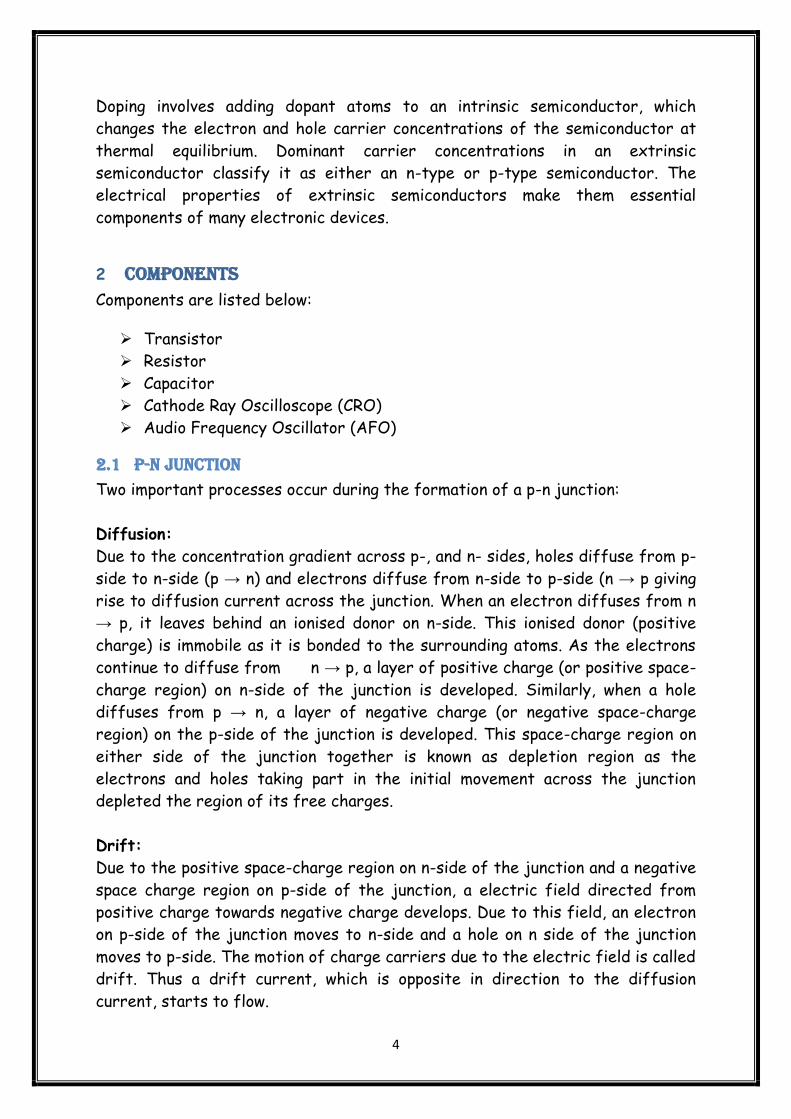
2.1 P-N Junction
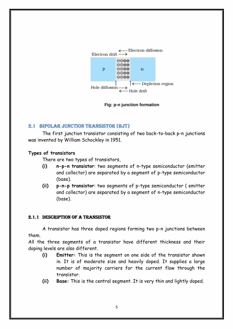
Two important processes occur during the formation of a p-n junction:
Diffusion:
Due to the concentration gradient across p-, and n- sides, holes diffuse from p-
side to n-side (p → n) and electrons diffuse from n-side to p-side (n → p giving
rise to diffusion current across the junction. When an electron diffuses from n
→ p, it leaves behind an ionised donor on n-side. This ionised donor (positive
charge) is immobile as it is bonded to the surrounding atoms. As the electrons
continue to diffuse from n → p, a layer of positive charge (or positive space-
charge region) on n-side of the junction is developed. Similarly, when a hole
diffuses from p → n, a layer of negative charge (or negative space-charge
region) on the p-side of the junction is developed. This space-charge region on
either side of the junction together is known as depletion region as the
electrons and holes taking part in the initial movement across the junction
depleted the region of its free charges.
Drift:
Due to the positive space-charge region on n-side of the junction and a negative
space charge region on p-side of the junction, a electric field directed from
positive charge towards negative charge develops. Due to this field, an electron
on p-side of the junction moves to n-side and a hole on n side of the junction
moves to p-side. The motion of charge carriers due to the electric field is called
drift. Thus a drift current, which is opposite in direction to the diffusion
current, starts to flow.
5
2.1 Bipolar Junction Transistor (BJT)
The first junction transistor consisting of two back-to-back p-n junctions
was invented by William Schockley in 1951.
Types of transistors
There are two types of transistors,
(i) n-p-n transistor: two segments of n-type semiconductor (emitter
and collector) are separated by a segment of p-type semiconductor
(base).
(ii) p-n-p transistor: two segments of p-type semiconductor ( emitter
and collector) are separated by a segment of n-type semiconductor
(base).
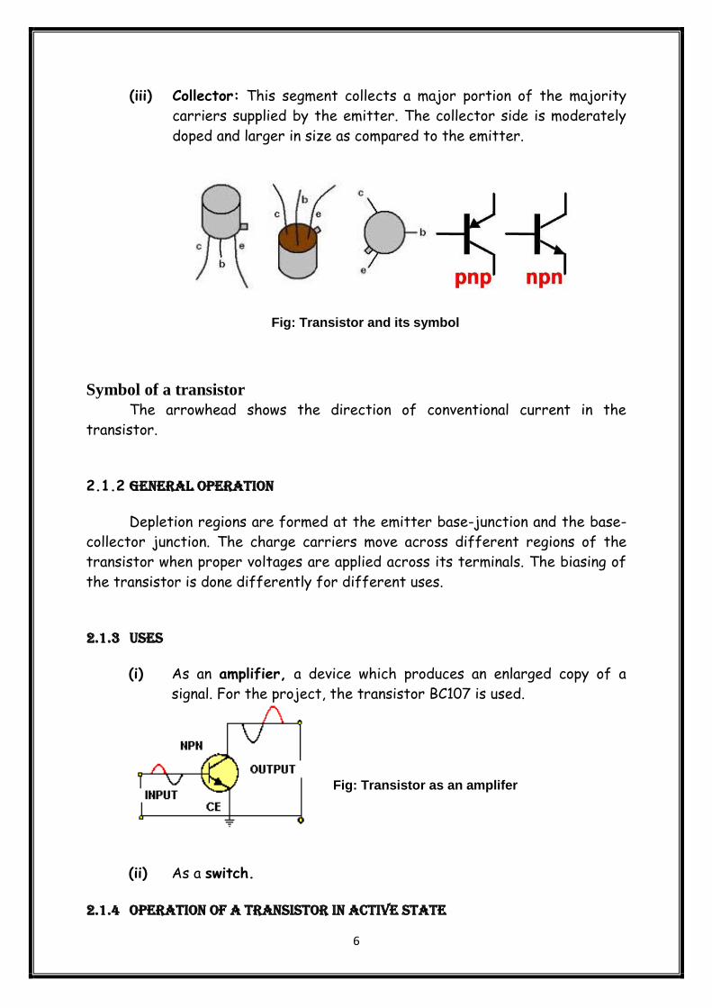
2.1.1 Description of a transistor
A transistor has three doped regions forming two p-n junctions between
them.
All the three segments of a transistor have different thickness and their
doping levels are also different.
(i) Emitter: This is the segment on one side of the transistor shown
in. It is of moderate size and heavily doped. It supplies a large
number of majority carriers for the current flow through the
transistor.
(ii) Base: This is the central segment. It is very thin and lightly doped.
Fig: p-n junction formation
6
(iii) Collector: This segment collects a major portion of the majority
carriers supplied by the emitter. The collector side is moderately
doped and larger in size as compared to the emitter.
Symbol of a transistor
The arrowhead shows the direction of conventional current in the
transistor.
2.1.2 General Operation
Depletion regions are formed at the emitter base-junction and the base-
collector junction. The charge carriers move across different regions of the
transistor when proper voltages are applied across its terminals. The biasing of
the transistor is done differently for different uses.
2.1.3 Uses
(i) As an amplifier, a device which produces an enlarged copy of a
signal. For the project, the transistor BC107 is used.
(ii) As a switch.
2.1.4 Operation of a transistor in Active state
Fig: Transistor and its symbol
Fig: Transistor as an amplifer
7
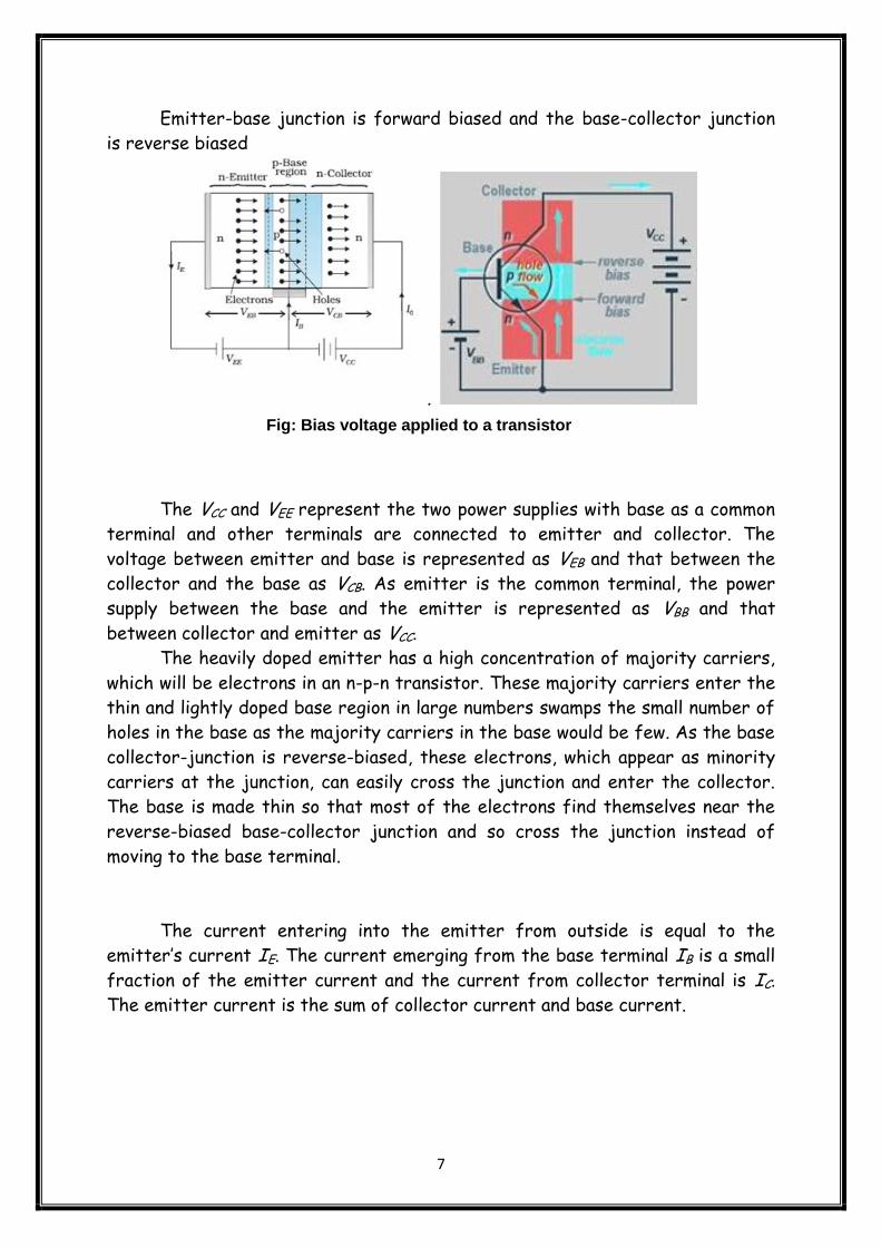
Emitter-base junction is forward biased and the base-collector junction
is reverse biased
.
The VCC and VEE represent the two power supplies with base as a common
terminal and other terminals are connected to emitter and collector. The
voltage between emitter and base is represented as VEB and that between the
collector and the base as VCB. As emitter is the common terminal, the power
supply between the base and the emitter is represented as VBB and that
between collector and emitter as VCC.
The heavily doped emitter has a high concentration of majority carriers,
which will be electrons in an n-p-n transistor. These majority carriers enter the
thin and lightly doped base region in large numbers swamps the small number of
holes in the base as the majority carriers in the base would be few. As the base
collector-junction is reverse-biased, these electrons, which appear as minority
carriers at the junction, can easily cross the junction and enter the collector.
The base is made thin so that most of the electrons find themselves near the
reverse-biased base-collector junction and so cross the junction instead of
moving to the base terminal.
The current entering into the emitter from outside is equal to the
emitter’s current IE. The current emerging from the base terminal IB is a small
fraction of the emitter current and the current from collector terminal is IC.
The emitter current is the sum of collector current and base current.
Fig: Bias voltage applied to a transistor
8
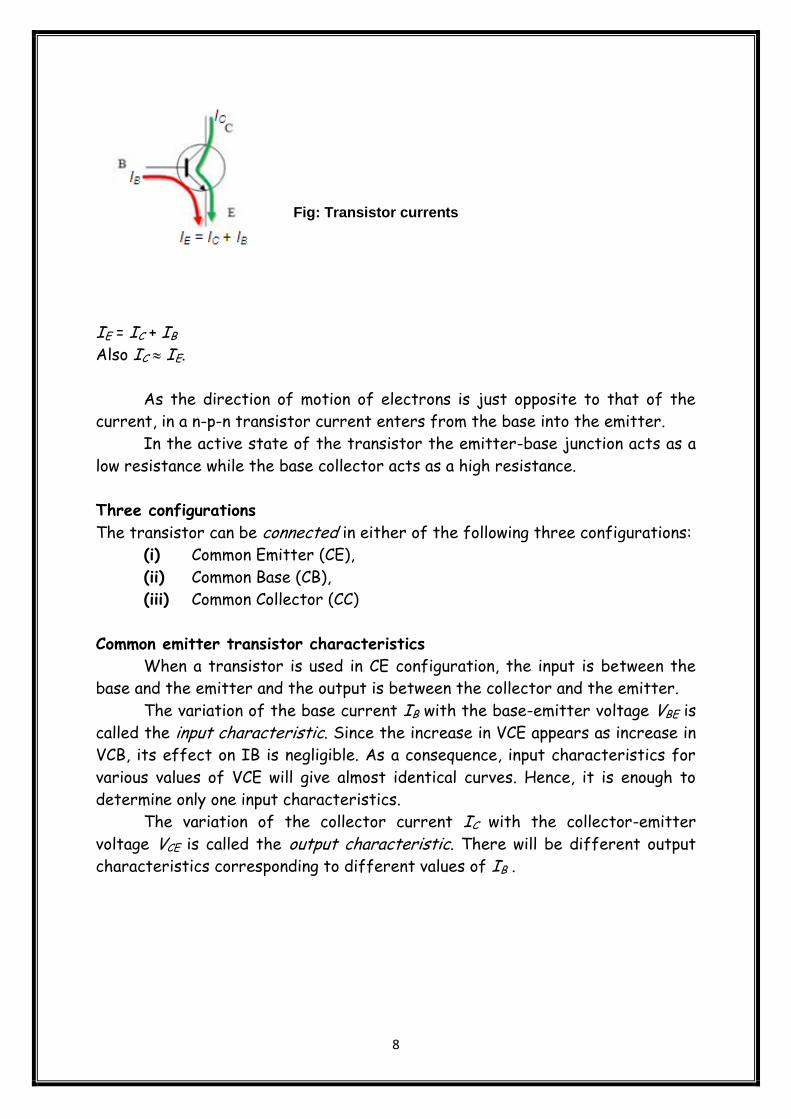
IE = IC + IB
Also IC IE.
As the direction of motion of electrons is just opposite to that of the
current, in a n-p-n transistor current enters from the base into the emitter.
In the active state of the transistor the emitter-base junction acts as a
low resistance while the base collector acts as a high resistance.
Three configurations
The transistor can be connected in either of the following three configurations:
(i) Common Emitter (CE),
(ii) Common Base (CB),
(iii) Common Collector (CC)
Common emitter transistor characteristics
When a transistor is used in CE configuration, the input is between the
base and the emitter and the output is between the collector and the emitter.
The variation of the base current IB with the base-emitter voltage VBE is
called the input characteristic. Since the increase in VCE appears as increase in
VCB, its effect on IB is negligible. As a consequence, input characteristics for
various values of VCE will give almost identical curves. Hence, it is enough to
determine only one input characteristics.
The variation of the collector current IC with the collector-emitter
voltage VCE is called the output characteristic. There will be different output
characteristics corresponding to different values of IB .
Fig: Transistor currents
9
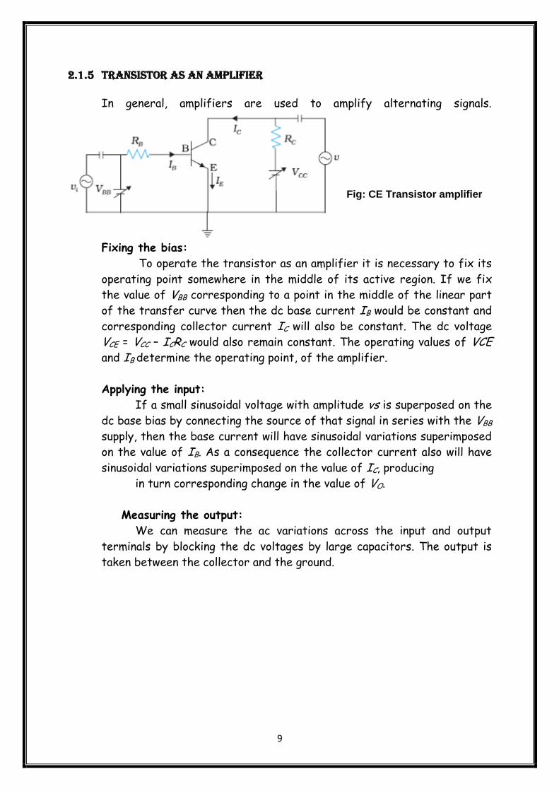
2.1.5 Transistor as an amplifier
In general, amplifiers are used to amplify alternating signals.
Fixing the bias:
To operate the transistor as an amplifier it is necessary to fix its
operating point somewhere in the middle of its active region. If we fix
the value of VBB corresponding to a point in the middle of the linear part
of the transfer curve then the dc base current IB would be constant and
corresponding collector current IC will also be constant. The dc voltage
VCE = VCC – ICRC would also remain constant. The operating values of VCE and IB determine the operating point, of the amplifier.
Applying the input:
If a small sinusoidal voltage with amplitude vs is superposed on the
dc base bias by connecting the source of that signal in series with the VBB supply, then the base current will have sinusoidal variations superimposed
on the value of IB. As a consequence the collector current also will have
sinusoidal variations superimposed on the value of IC, producing
in turn corresponding change in the value of VO.
Measuring the output:
We can measure the ac variations across the input and output
terminals by blocking the dc voltages by large capacitors. The output is
taken between the collector and the ground.
Fig: CE Transistor amplifier
10
2.2 RESISTOR
A resistor is an electrical component designed to have an electrical
resistance that is independent of the current flowing through it. The common
type of resistor is also designed to be independent of temperature and other
factors. Resistors may be fixed or variable. Variable resistors are also
called potentiometers or rheostats
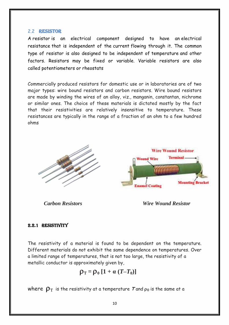
Commercially produced resistors for domestic use or in laboratories are of two
major types: wire bound resistors and carbon resistors. Wire bound resistors
are made by winding the wires of an alloy, viz., manganin, constantan, nichrome
or similar ones. The choice of these materials is dictated mostly by the fact
that their resistivities are relatively insensitive to temperature. These
resistances are typically in the range of a fraction of an ohm to a few hundred
ohms
Carbon Resistors Wire Wound Resistor
2.2.1 Resistivity
The resistivity of a material is found to be dependent on the temperature.
Different materials do not exhibit the same dependence on temperatures. Over
a limited range of temperatures, that is not too large, the resistivity of a
metallic conductor is approximately given by,
= 0 [1 + α (T–T0)]
where is the resistivity at a temperature T and 0 is the same at a
11
reference temperature T0. α is called the temperature co-efficient of resistivity, and the dimension of α is (Temperature)–1.
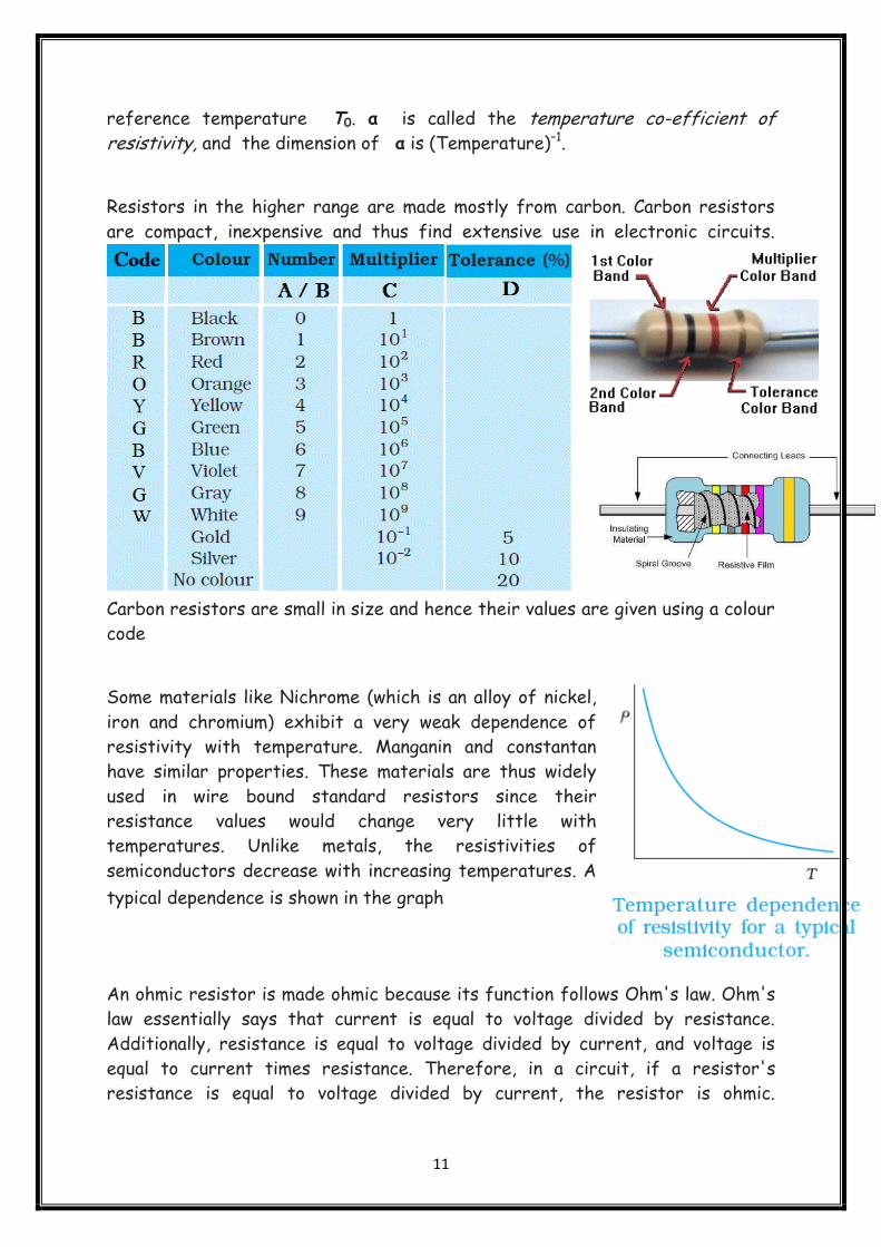
Resistors in the higher range are made mostly from carbon. Carbon resistors
are compact, inexpensive and thus find extensive use in electronic circuits.
Carbon resistors are small in size and hence their values are given using a colour
code
Some materials like Nichrome (which is an alloy of nickel,
iron and chromium) exhibit a very weak dependence of
resistivity with temperature. Manganin and constantan
have similar properties. These materials are thus widely
used in wire bound standard resistors since their
resistance values would change very little with
temperatures. Unlike metals, the resistivities of
semiconductors decrease with increasing temperatures. A
typical dependence is shown in the graph
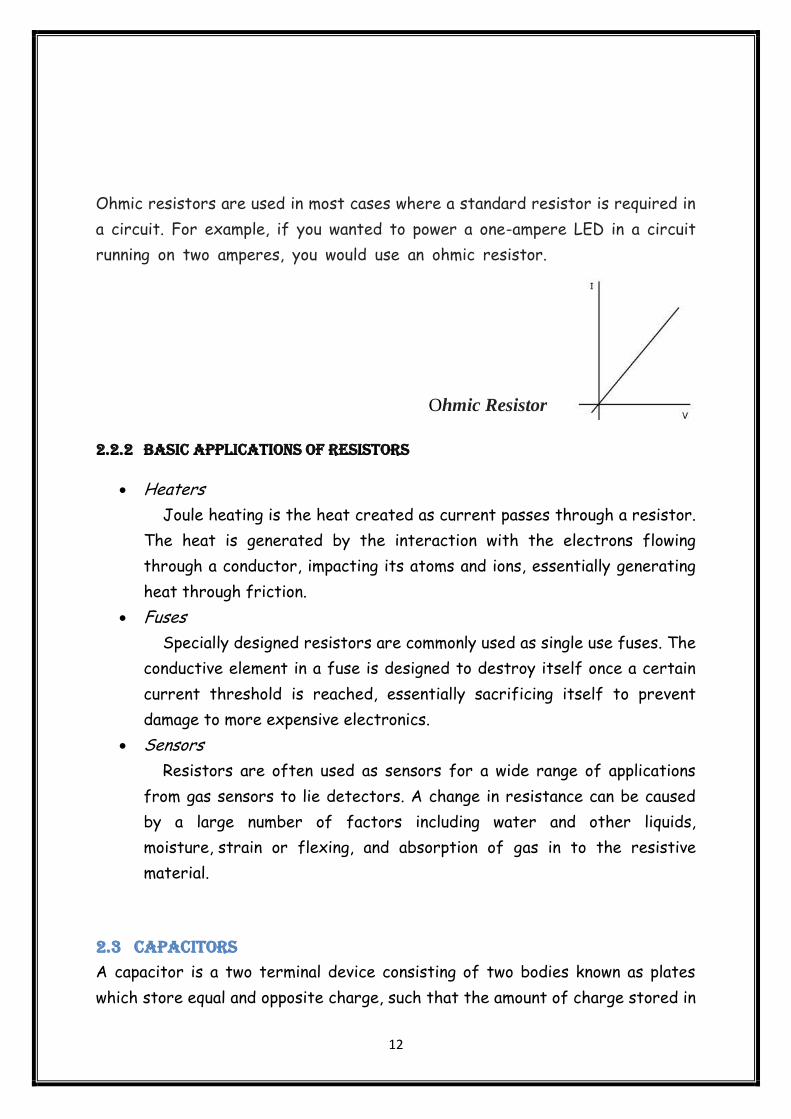
An ohmic resistor is made ohmic because its function follows Ohm's law. Ohm's
law essentially says that current is equal to voltage divided by resistance.
Additionally, resistance is equal to voltage divided by current, and voltage is
equal to current times resistance. Therefore, in a circuit, if a resistor's
resistance is equal to voltage divided by current, the resistor is ohmic.
12
Ohmic resistors are used in most cases where a standard resistor is required in
a circuit. For example, if you wanted to power a one-ampere LED in a circuit
running on two amperes, you would use an ohmic resistor.
Ohmic Resistor
2.2.2 Basic Applications Of Resistors
Heaters
Joule heating is the heat created as current passes through a resistor.
The heat is generated by the interaction with the electrons flowing
through a conductor, impacting its atoms and ions, essentially generating
heat through friction.
Fuses
Specially designed resistors are commonly used as single use fuses. The
conductive element in a fuse is designed to destroy itself once a certain
current threshold is reached, essentially sacrificing itself to prevent
damage to more expensive electronics.
Sensors
Resistors are often used as sensors for a wide range of applications
from gas sensors to lie detectors. A change in resistance can be caused
by a large number of factors including water and other liquids,
moisture, strain or flexing, and absorption of gas in to the resistive
material.
2.3 CAPACITORS
A capacitor is a two terminal device consisting of two bodies known as plates
which store equal and opposite charge, such that the amount of charge stored in
13
each plate of the capacitor is directly proportional to the potential difference
across the plates (terminals) of the capacitor, and the proportionality constant
is called capacitance.
Capacitors vary in shape and size, but the basic configuration is two conductors
carrying equal but opposite charges. Capacitors have many important
applications in electronics. Some examples include storing electric potential
energy, delaying voltage changes when coupled with resistors, filtering out
unwanted frequency signals, forming resonant circuits and making frequency-
dependent and independent voltage dividers when combined with resistors.
The conductors may be so charged by connecting them to the two terminals of a
battery. Q is called the charge of the capacitor, though this, in fact, is the
charge on one of the conductors – the total charge of the capacitor is zero. The
electric field in the region between the conductors is proportional to the charge
Q. That is, if the charge on the capacitor is, say doubled, the electric field will
also be doubled at every point. (This follows from the direct proportionality
between field and charge implied by Coulomb’s law and the superposition
principle.)
2.3.1 HOW CAPACITORS WORK
When the voltage from a source such as a battery is connected, the negative
side of the battery voltage immediately begins to push negative charges toward
one of the plates. Simultaneously, the positive side of the battery voltage
begins to pull electrons (negative charges) away from the second plate.
What permits current to flow is the electric field that quickly builds up
between the two plates. As the plate on the negative side of the circuit fills
with electrons, the electric field created by those electrons begins to push
electrons away from the plate on the other side of the insulator, toward the
positive side of the battery voltage.
As this current flows, the negative plate of the capacitor builds up an excess of
electrons, whereas the positive side develops a corresponding deficiency of
electrons. Thus, voltage is developed between the two plates of the capacitor.
But there's a catch: This current flows only for a brief time. As the electrons
build up on the negative plate and are depleted from the positive plate, the
14
voltage between the two plates increases because the difference in charge
between the two plates increases.
The voltage continues to increase until the capacitor voltage equals the battery
voltage. Once the voltages are the same, current stops flowing through the
circuit, and the capacitor is said to be charged.
Also, once a capacitor has been charged, you can disconnect the battery from
the capacitor, and the voltage will remain in the capacitor. In other words,
although the voltage in the capacitor is created by the battery, this voltage
isn't dependent on the battery for its continued existence. Disconnect the
battery, and the voltage remains across the two plates of the capacitor.
Thus, capacitors have the ability to store charge — an ability known as
capacitance.
2.3.2 TYPES
The capacitance of a capacitor purely depends on the geometry of the capacitor
and the medium in which it is placed. A few common types are 9based on
geometry:
Cylindrical capacitors
Parallel plate capacitor
Spherical capacitors
Based on material they are classified as:
Air - Often used in radio tuning circuits
Mylar - Most commonly used for timer circuits like clocks, alarms and
counters
Glass - Good for high voltage applications
Ceramic - Used for high frequency purposes like antennas, X-ray and MRI
machines
Super capacitor - Powers electric and hybrid cars
15
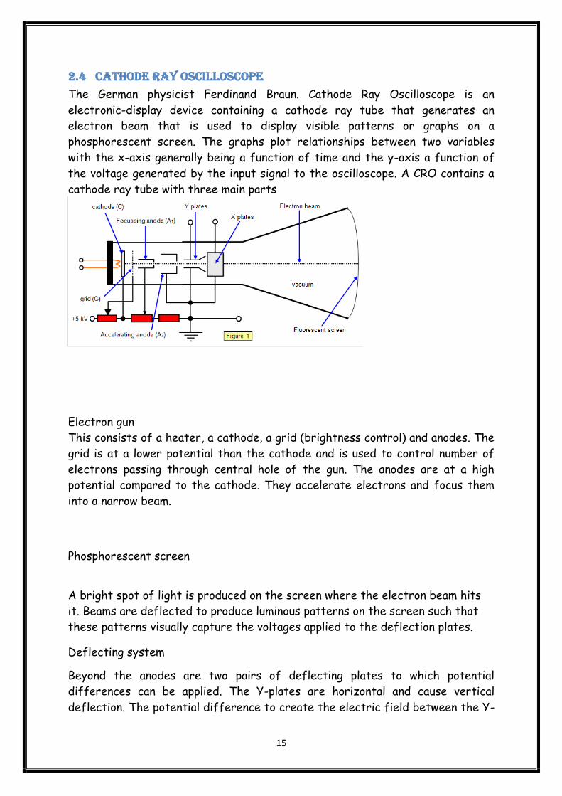
2.4 CATHODE RAY OSCILLOSCOPE
The German physicist Ferdinand Braun. Cathode Ray Oscilloscope is an
electronic-display device containing a cathode ray tube that generates an
electron beam that is used to display visible patterns or graphs on a
phosphorescent screen. The graphs plot relationships between two variables
with the x-axis generally being a function of time and the y-axis a function of
the voltage generated by the input signal to the oscilloscope. A CRO contains a
cathode ray tube with three main parts
Electron gun
This consists of a heater, a cathode, a grid (brightness control) and anodes. The
grid is at a lower potential than the cathode and is used to control number of
electrons passing through central hole of the gun. The anodes are at a high
potential compared to the cathode. They accelerate electrons and focus them
into a narrow beam.
Phosphorescent screen
A bright spot of light is produced on the screen where the electron beam hits
it. Beams are deflected to produce luminous patterns on the screen such that
these patterns visually capture the voltages applied to the deflection plates.
Deflecting system
Beyond the anodes are two pairs of deflecting plates to which potential
differences can be applied. The Y-plates are horizontal and cause vertical
deflection. The potential difference to create the electric field between the Y-
16
plates is applied to the Y-input terminal. The input is usually amplified to give
suitable vertical deflection. The vertical plates are called the X-plates and they
produce horizontal deflection. The potential difference applied to the X-plates
is also amplified by an amplifier – the X-amplifier, and is commonly from the
time base circuit of the CRO. The time base circuit of the CRO applies a wave
saw-tooth waveform to the X-plates. The beam is moved from the left hand side
to the right in the time that the voltage rises to a maximum, and then is
returned rapidly to the left as the voltage returns to zero. Alternatively the
electron beam may also be deflected magnetically through externally mounted
deflection coils.
2.4.1 Uses of CRO
1) Voltage Measurements
The oscilloscope must first be calibrated with by connecting a dc source of
known emf to the Y-plates and measuring the deflection of the spot on the
screen. By repeating this process by altering the known emf, the linearity of the
deflections, in Volts per meter can be found.
2) Displaying waveforms
In this role, the time base is on. The CRO acts as a graph-plotter to show the
waveform i.e. the variation of potential difference applied across the Y-plates
with time.
3) Frequency Measurements
Measurement of frequency is enabled by a calibrated time base. If the time
base is set at a certain value in time per length for a waveform, one complete
waveform occupies two units of length. Therefore twice the value at which the
time base is set is the time period of the waveform. The reciprocal of the time-
period is the frequency of the waveform.
2.5 AUDIO FREQUENCY OSCILLATOR (AFO)
Audio Frequency Oscillator (AF Oscillator), also known as audio oscillator, is a
useful test instrument capable of generating sine, and also square & triangle
waveforms at any required frequency within audible range of average human
being. The generally accepted standard range of audible frequency of human is
20Hz – 20KHz.
Oscillators come with different waveforms, which determine how it varies.
Some, such as sine wave oscillators are smooth whereas others are sharp and
sudden, like square wave oscillators.
17
An AFO merely produces an oscillation in voltage, not air pressure. Hence we
cannot hear it directly. In order to hear it, the AFO needs to be connected to a
speaker through the output terminals.
An AFO uses an electron tube, transistor, or other nonrotating device to
produce an audio-frequency alternating current. The instrument is provided with
output banana sockets and generally gives a maximum wave output of 20 volts
peak to peak approximately, which may be adjusted by an amplitude control
potentiometer. The frequency of the signal source is set on a dial (1 to 11)
provided with the AFO, along with a multiplier range switch (x1, x10, x100, x1K,
x10K, x100K).
General specifications of an AFO may be stated as,
Frequency range : 20Hz to 20KHz (audible range)
Wave forms : Sine, Square, Triangle waveforms
Output Amplitude : 0-20V peak to peak variable ± 3% approx.
Power Supply : 220 Volts
2.5.1 Applications of AF Oscillators
AFO’s are widely used in electronic industry and educational institutions
AFO's are often used as test signal sources in laboratories and research
facilities.
Variable frequency oscillators are used in audio signal generators that are
essential for testing amplifiers and fault tracing in many electronics
18
3 AMPLIFIER
An electronic amplifier is an electronic device that increases the power of
a signal. It does this by taking energy from a power supply and controlling the
output to match the input signal shape but with a larger amplitude. In this
sense, an amplifier modulates the output of the power supply.
There are four basic types of electronic amplifier: the voltage amplifier,
the current amplifier, the transconductance amplifier, and the transresistance
amplifier.
3.1 Power amplifier
The term power amplifier is a relative term with respect to the amount of
power delivered to the load and/or provided by the power supply circuit. In
general the power amplifier is the last 'amplifier' or actual circuit in a signal
chain (the output stage) and is the amplifier stage that requires attention to
power efficiency.
3.2 Transistor amplifiers
The essential role of this active element is to magnify an input signal to yield a
significantly larger output signal. The amount of magnification (the "forward
gain") is determined by the external circuit design as well as the active device.
Applications are numerous, some common examples are audio amplifiers in a
home stereo or PA system, RF high power generation for semiconductor
equipment, to RF and Microwave applications such as radio transmitters
3.3 Oscilloscope vertical amplifiers
These deal with video signals that drive an oscilloscope display tube, and can
have bandwidths of about 500 MHz.
19
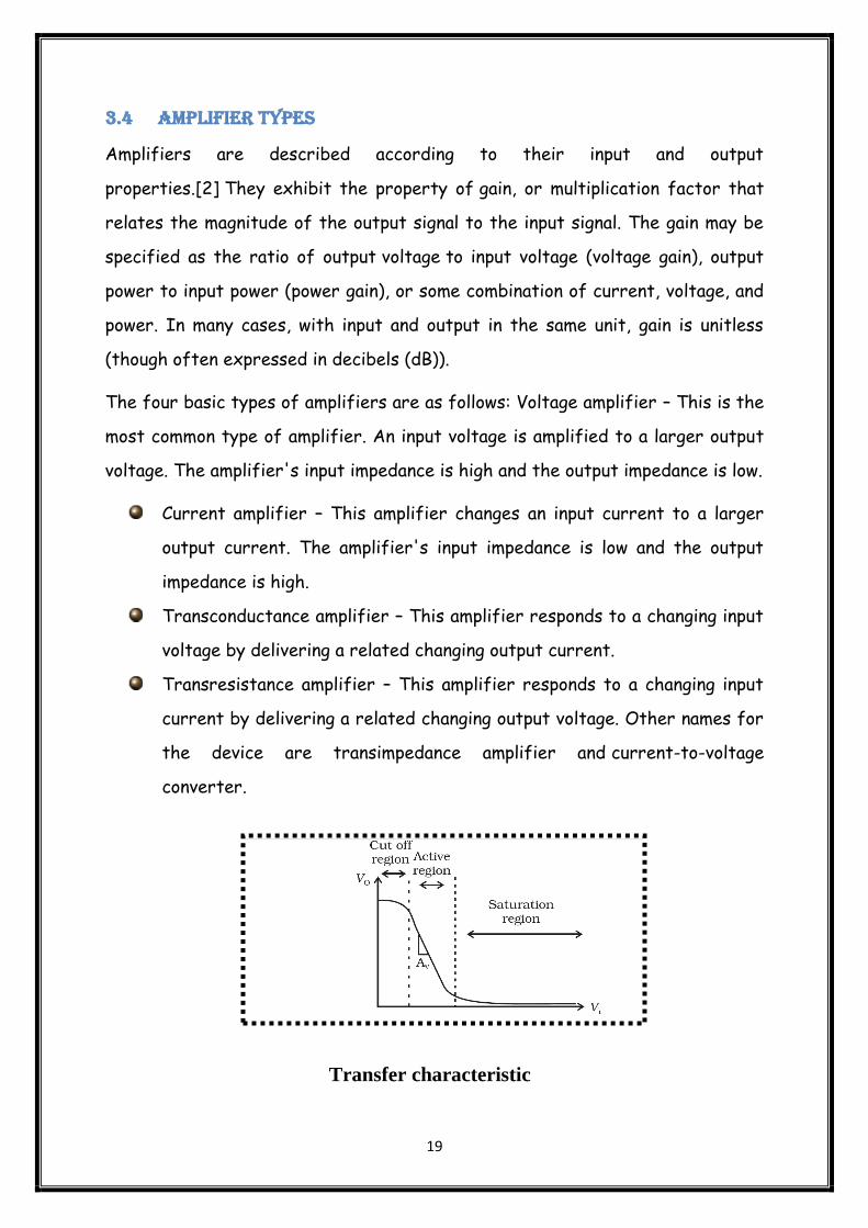
3.4 Amplifier types
Amplifiers are described according to their input and output
properties.[2] They exhibit the property of gain, or multiplication factor that
relates the magnitude of the output signal to the input signal. The gain may be
specified as the ratio of output voltage to input voltage (voltage gain), output
power to input power (power gain), or some combination of current, voltage, and
power. In many cases, with input and output in the same unit, gain is unitless
(though often expressed in decibels (dB)).
The four basic types of amplifiers are as follows: Voltage amplifier – This is the
most common type of amplifier. An input voltage is amplified to a larger output
voltage. The amplifier's input impedance is high and the output impedance is low.
Current amplifier – This amplifier changes an input current to a larger
output current. The amplifier's input impedance is low and the output
impedance is high.
Transconductance amplifier – This amplifier responds to a changing input
voltage by delivering a related changing output current.
Transresistance amplifier – This amplifier responds to a changing input
current by delivering a related changing output voltage. Other names for
the device are transimpedance amplifier and current-to-voltage
converter.
Transfer characteristic
20
3.5 Transistor as an amplifier
For using the transistor as an amplifier we will use the active region of the Vo
versus Vi curve. The slope of the linear part of the curve represents the rate of
change of the output with the input. It is negative because the output is VCC –
ICRC and not ICRC. That is why as input voltage of the CE amplifier increases
its output voltage decreases and the output is said to be out of phase with the
input. If we consider ΔVo and ΔVi as small changes in the output and input
voltages then ΔVo/ΔVi is called the small signal voltage gain AV of the
amplifier. If the VBB voltage has a fixed value corresponding to the mid point
of the active region, the circuit will behave as a CE amplifier with voltage gain
ΔVo/ ΔVi. We can express the voltage gain AV in terms of the resistors in the
circuit and the current gain of the transistor as follows.
We have, Vo = VCC – ICRC
Therefore, ΔVO = 0 – RCΔ Ic
Similarly, from Vi = IBRB + VBE
ΔVi= RB ΔIB + ΔVBE
But ΔVBE is negligibly small in comparison to ΔIBRB in this circuit.
So, the voltage gain of this CE amplifier is given by
AV = – RC Δ IC / RB ΔIB
= –βac(RC/RB )
where βac is equal to Δ IC/ΔIB . Thus the linear portion of the active region of
the transistor can be exploited for the use in amplifiers. Transistor as an
amplifier (CE configuration) is discussed in detail in the next section.
The most common way to use a transistor as an amplifier is in an electronic
circuit sometimes called a common-emitter circuit because the emitter is
connected to ground, which means that both the input signal and the output
signal share the emitter connection.
Below circuit uses a pair of resistors as a voltage divider to control exactly how
much voltage is placed across the base and emitter of the transistor. The AC
signal from the input is then superimposed on this bias voltage to vary the bias
current. Then, the amplified output is taken from the collector and emitter.
Variations in the bias current are amplified in the output current.
21
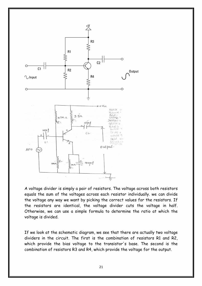
A voltage divider is simply a pair of resistors. The voltage across both resistors
equals the sum of the voltages across each resistor individually. we can divide
the voltage any way we want by picking the correct values for the resistors. If
the resistors are identical, the voltage divider cuts the voltage in half.
Otherwise, we can use a simple formula to determine the ratio at which the
voltage is divided.
If we look at the schematic diagram, we see that there are actually two voltage
dividers in the circuit. The first is the combination of resistors R1 and R2,
which provide the bias voltage to the transistor's base. The second is the
combination of resistors R3 and R4, which provide the voltage for the output.
22
This second voltage divider is a variable voltage divider: The ratio of the
resistances changes based on the bias voltage, which means the voltage at the
collector varies as well. The amplification occurs because very small variations in
an input signal are reflected in much larger variations in the output signal.
Looking at this circuit more closely:
The input arrives at the left side of the circuit in the form of a signal,
which usually has both a DC and an AC component. In other words, the
voltage fluctuates but never goes negative.
One side of the input is connected to ground, to which the battery's
negative terminal is also connected. The transistor's emitter is also
connected to ground (through a resistor), as is one side of the output.
The purpose of C1 is to block the DC component of the input signal. Only
pure AC gets past the capacitor. Without this capacitor, any DC voltage in
the input signal would be added to the bias voltage applied to the
transistor, which could spoil the transistor's ability to faithfully amplify
the AC part of the input signal.
R1 and R2 form a voltage divider that determines how much DC voltage is
applied to the transistor base. The AC portion of the signal that gets
past C1 is combined with this DC voltage, which causes the transistor's
base current to vary with the voltage.
R3, R4, and the variable resistance of the collector-emitter circuit form
a voltage divider on the output side of the amplifier. Amplification occurs
because the full power supply voltage is applied across the output circuit.
The varying resistance of the collector-emitter path reflects the small
AC input signal on the much larger output signal.
C2 blocks the DC component of the output signal so that only pure AC is
passed on to the next stage of the amplifier circuit.
23
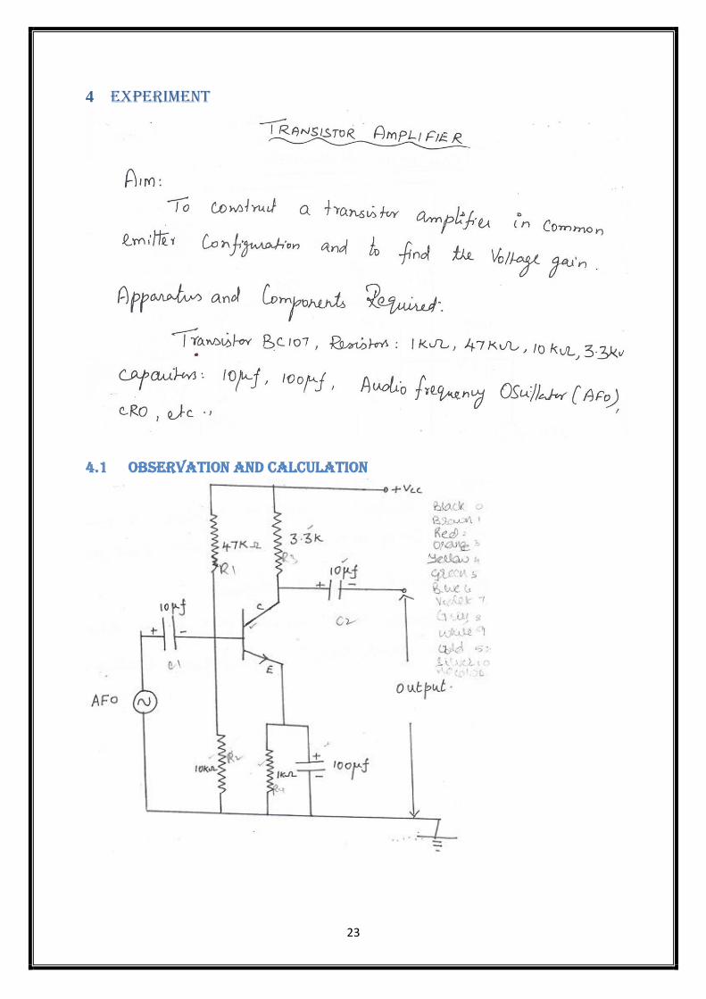
4 EXPERIMENT
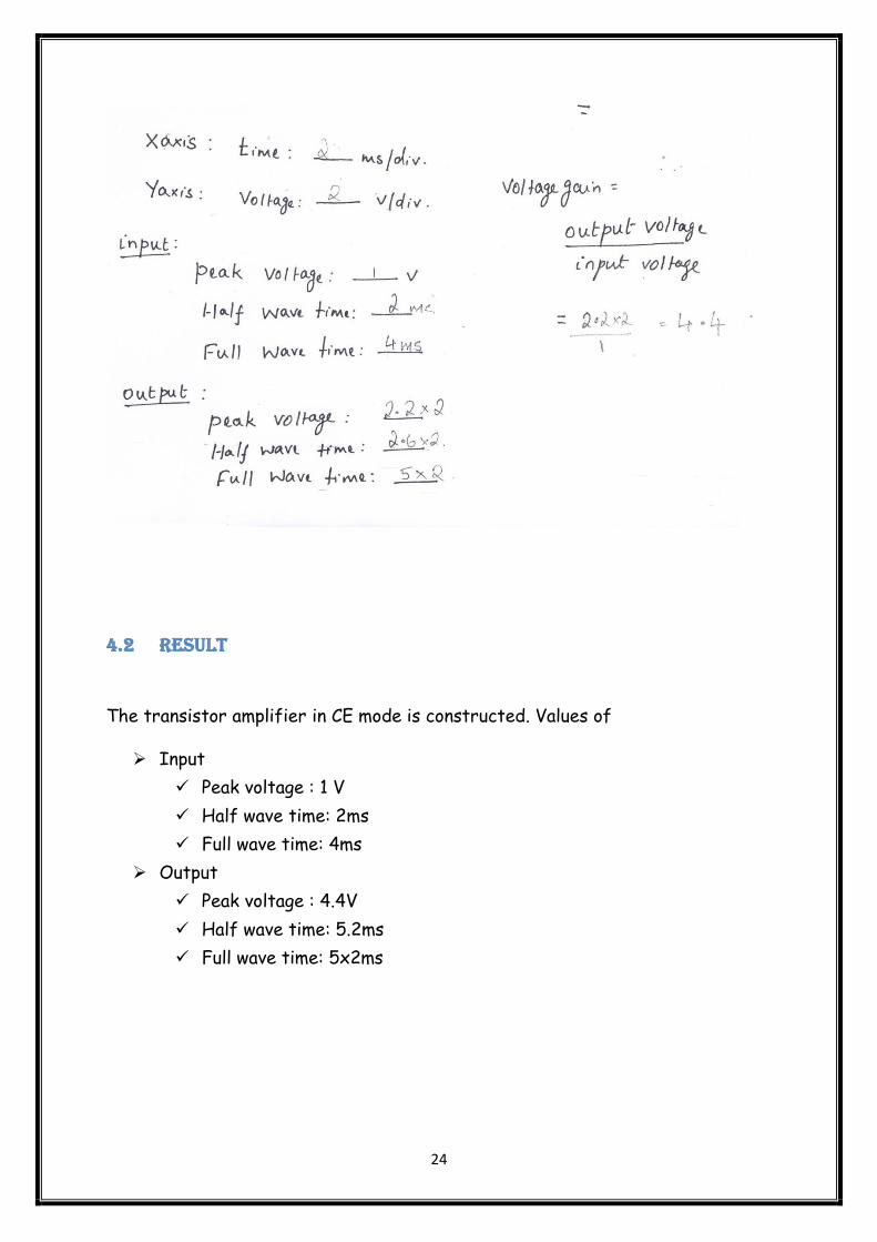
4.1 OBSERVATION AND CALCULATION
24
4.2 Result
The transistor amplifier in CE mode is constructed. Values of
Input
Peak voltage : 1 V
Half wave time: 2ms
Full wave time: 4ms
Output
Peak voltage : 4.4V
Half wave time: 5.2ms
Full wave time: 5x2ms
25
4.3 GRAPH
26
5 Applications of Amplifiers
5.1 Purpose
Used for amplification i.e. the process of increasing the amplitude (and
consequently the strength) of a signal. Amplifiers are capable of increasing the
power, voltage or current of a signal. It comprises of an electronic circuit and is
necessary for the compensation of the attenuation of signals in communication
using a DC power source.
The amplifier plays a role at locations between the source and the
destination wherever the signal strength becomes weaker than the
required strength.
5.2 Applications
Amplifiers are generally seen in audio systems where signals are
repeatedly converted from electrical signals to audio signals and vice
versa. During the conversion, amplifiers set the signal to the frequency
required for the specific device.
The common emitter amplifier is commonly used and is used in transistor
circuits where voltage gain is required.
The common-emitter amplifier is designed so that a small change in the
input voltage (Vin) changes the small current through the base of the
transistor; the transistor's current amplification combined with the
properties of the circuit mean that small swings in Vin produce large
changes in Vout (output voltage).
Amplifiers are used in devices that transmit signals as well as devices
that receive signals.
Amplifiers are used in devices like mobile phones and televisions for
sound reproduction, radio transmission, and signal processing.
27
When the power dissipated across the resistor in the amplifier circuit is
more than the supply power, the amplifier is a power amplifier.
In the common emitter amplifier, the voltage across the resistor in the
amplifier circuit is more than the input voltage.
28
6 BIBLIOGRAPHY
www.howstuffworks.com
www.electronicstutorials
hyperphysics.phy-astr.gsu.edu/hbase/solids/trans.html
www.britannica.com/
www.ncert.nic.in