Embed Size (px)
Citation preview

1
Physical properties of transparent perovskite oxides (Ba,La)SnO3 with high electrical mobility at room temperature
Hyung Joon Kim1, Useong Kim2, Tai Hoon Kim1, Jiyeon Kim2, Hoon Min Kim2, Byung-Gu Jeon1, Woong-Jhae Lee1, Hyo Sik Mun2, Kwang Taek Hong1, Jaejun Yu2, Kookrin Char2†
and Kee Hoon Kim1†
1Center for Novel States of Complex Materials Research, Department of Physics and Astronomy, Seoul National University, Seoul 151-747, Republic of Korea
2Center for Strongly Correlated Materials Research, Department of Physics and Astronomy, Seoul National University, Seoul 151-747, Republic of Korea
ABSTRACT
Transparent electronic materials are increasingly in demand for a variety of optoelectronic
applications, ranging from passive transparent conductive windows to active thin film transistors.
BaSnO3 is a semiconducting oxide with a large band gap of more than 3.1 eV. Recently, we
discovered that BaSnO3 doped with a few percent of La exhibits unusually high electrical mobility of
320 cm2(Vs)-1 at room temperature and superior thermal stability at high temperatures [H. J. Kim et al.
Appl. Phys. Express. 5, 061102 (2012)]. Following that work, we report here various physical
properties of (Ba,La)SnO3 single crystals and epitaxial films including temperature-dependent
transport and phonon properties, optical properties and first-principles calculations. We find that
almost doping-independent mobility of 200-300 cm2(Vs)-1 is realized in the single crystals in a broad
doping range from 1.01019 to 4.01020 cm-3. Moreover, the conductivity of ~104 -1cm-1 reached at
the latter carrier density is comparable to the highest value previously reported in the transparent
conducting oxides. We attribute the high mobility to several physical properties of (Ba,La)SnO3: a
small effective mass coming from the ideal Sn-O-Sn bonding in a cubic perovskite network, small
disorder effects due to the doping away from the SnO2 conduction path, and reduced carrier scattering
due to the high dielectric constant. The observation of a reduced mobility of ~ 70 cm2(Vs)-1 in the
epitaxial films is mainly attributed to additional carrier-scattering due to dislocations and grain

2
boundaries, which are presumably created by the lattice mismatch between the substrate SrTiO3 and
(Ba,La)SnO3. The main optical gap coming from the charge transfer from O 2p to Sn 5s bands in
(Ba,La)SnO3 single crystals remained at about 3.33 eV and the in-gap states only slightly increased,
thus maintaining optical transparency in the visible spectral region. Based on all these results, we
suggest that the doped BaSnO3 system holds great potential for realizing all perovskite-based,
transparent high-temperature high-power functional devices as well as highly mobile two-dimensional
electron gas via interface control of heterostructured films.
PACS number: 81.05.Hd, 71.20.Nr, 72.10.Bg, 72.20.Dp, 78.40.Fy

3
I. INTRODUCTION
Transparent oxide materials offer great potential for a wide range of device applications, e.g.
transparent conductive windows for solar cells, flat panel displays, light emitting diodes, and
transparent logic devices. Numerous oxide materials including ZnO, In2O3, and SnO2 have been
investigated for these purposes, successfully demonstrating passive conducting leads to active
semiconducting devices such as pn junctions, field effect transistors, and UV lasers.1-8 However, these
well-known material systems still have limitations so that there is currently active scientific research
to find alternative transparent materials which can potentially exhibit better physical properties. For
example, high mobility is one essential ingredient for developing transparent logic devices with high
density, and oxygen stability is also crucial to overcome interface degradation problems in the oxide
pn junctions. Moreover, controlling and minimizing the density of defects or dislocations becomes
also important to realize useful devices based on transparent conducting oxides (TCOs) and
transparent oxide semiconductors (TOSs).
Oxide materials with the perovskite structure have exhibited a plethora of interesting physical
properties such as superconductivity, colossal magnetoresistance, ferroelectricity, piezoelectricity, and
multiferroicity.9-12 Extensive research efforts have been made to utilize such varied physical properties
in the form of thin film heterostructures.13 The perovskite materials have also been investigated in the
context of searching for new TCOs and TOSs as doped SrTiO3 and doped CaTiO3.14-18 The alkaline
earth stannates with a chemical formula ASnO3 (A = Ba, Sr, and Ca) are another perovskite system
that has been used in industry for photoelectrochemical energy conversions, stable capacitors, and gas
sensors.19-21. In particular, BaSnO3 is known to form an ideal cubic perovskite structure (See, Fig.
1(a)), in which the Sn-O-Sn bonding angle is close to 180, and corresponds to a transparent, wide
band gap semiconductor with an optical gap of ~ 3.1 eV.22 In order to have electrical conduction in
BaSnO3, both Ba and Sn sites were doped to form compounds like (Ba,La)SnO3 and Ba(Sn,Sb)O3 in
polycrystalline or thin film forms.23-27 However, the reported electrical mobility in the thin film was
4
relatively low, less than 2 cm2(Vs)-1 and the conductivity reached at most 500 -1cm-1.26,27 As those
reported transport properties might not be intrinsic, possibly due to, e.g., grain boundary scattering or
off-stoichiometry, the growth of high quality single crystals of doped BaSnO3 and the study of their
intrinsic physical properties are of high interest.
Recently, we succeeded in growing single crystals28-29 of (Ba,La)SnO3 and Ba(Sn,Sb)O3 by the Cu2O-
flux method up to a lateral size of ~2 mm. In particular, we discovered that a (Ba,La)SnO3 single
crystal shows an unprecedentedly high electrical mobility of ~ 320 cm2(Vs)-1 with a carrier density of
1.01020 cm-3 at room temperature.28 In parallel with our discovery, there was a similar report on the
growth of (Ba,La)SnO3 single crystals by PbO and PbF2 flux,30 in which the highest electrical
mobility was found to be ~103 cm2(Vs)-1. We also found that the epitaxial thin films of (Ba,La)SnO3
grown on SrTiO3 (001) substrate shows an electrical mobility as high as 70 cm2(Vs)-1, which is much
larger than the previously reported values26,27 in thin films. Moreover, the resistivity of the
(Ba,La)SnO3 film has shown little change even at 500 C in air, which suggests extremely good
oxygen stability and related physical properties at high temperatures.28
In order to understand further the origins of such high mobility in the (Ba,La)SnO3 system, we
systematically report various physical properties of the single crystals and epitaxial films in the
following sections. In Sec. II, we describe the various experimental tools we have employed. In Sec.
III, we present experimental and theoretical results in wide doping ranges in the crystals and films,
including temperature-dependent transport properties, structural characteristics, band structure
calculations, and optical properties. From the Hall effect measurements in a broad doping range from
1.01019 to 4.01020 cm-3, we found that the mobility remains as high as ~200-300 cm2(Vs)-1 and does
not show clear dependence on the carrier density. In Sec. IV, we discuss mainly the possible physical
origins for obtaining the high electrical mobility. In Sec. V, we conclude that (Ba,La)SnO3 has a great
potential for being used as perovskite-based TOSs with high electrical mobility and superior thermal
stability.

5
II. EXPERIMENTAL
For the single crystal growth of Ba1-xLaxSnO3 (x = 0-0.04), the corresponding polycrystalline
specimen was first synthesized as a seed material. High purity BaCO3, SnO2, and La2O3 powders were
weighed in a stoichiometric ratio, thoroughly mixed in an agate mortar, and fired at 1250 oC for 6
hours. After several intermediate grindings, the powders were pressed into a pellet and sintered at
1400-1450 oC for 24-48 hours. For the growth of (Ba,La)SnO3 single crystals, the Cu2O flux and the
sintered powder were placed in a Pt crucible with a molar ratio of about 15:1 and were fired in air
above 1250 ºC and then slowly cooled down to 1210 º C, followed by a slow furnace cooling to room
temperature. The crystals show a cube-like shape as shown in Fig. 1(b).
We grew epitaxial films by use of the pulsed laser deposition technique, using BaSnO3,
Ba0.96La0.04SnO3, and Ba0.93La0.07SnO3 targets. We used single crystal SrTiO3 (001) as a substrate, and
performed the deposition in an O2 pressure of 100 mTorr at 750 oC. After the deposition, we cooled
the samples in an O2 pressure of about 600 mTorr.
We investigated the structural properties of the poly- and single-crystalline samples by use of X-ray
diffraction (XRD), for which we used a high power X-ray diffractometer equipped with a single Cu
K1 source (EmpyreanTM, PANalytical). We performed temperature-dependent X-ray diffraction
measurements for the polycrystalline powder of Ba0.999La0.001SnO3 by use of a closed-cycle cryostat
(PheniXTM, Oxford Instruments), operating in the 20-300 K temperature range. We also characterized
the structure of epitaxial films with a four-circle X-ray diffractometer.
The first-principles density functional theory (DFT) calculations were performed by using the
Vienna ab-initio Simulation Package (VASP) code.31 The projector-augmented-wave (PAW)
method32 and the Ceperley-Alder parameterization were employed within the local density
approximation (LDA).33 To determine the electronic structure of La-doped BaSnO3, we adopted a
333 supercell containing 135 atoms and carried out the k-space integration using a 222 mesh
within the Monkhorst-Pack k-point sampling. For the calculations, all atomic coordinates were

6
relaxed and the Hellmann-Feynman force reached to less than 0.02 eV Å-1. The cut-off energy used
for the plane wave basis set was 520 eV.
Temperature-dependent resistivity was measured by the conventional four-probe technique for the
single crystals and films from 2 K to 300 K either in a closed cycle refrigerator or in a physical
property measurement system (PPMSTM, Quantum Design). The five-wire configuration was
employed to investigate the Hall effect in single crystals and some thin films as a function of
temperatures in a magnetic field up to 9 tesla. To make electrical contacts, the single crystals
were cut and polished into a rectangular parallelepiped, of which lateral size and thickness
were typically ~ 1.50.8 mm2 and ~ 50 m, respectively, as shown in Fig. 1 (b). By use of a
shadow mask, we subsequently deposited 100 nm thick Au films as electrical pads on the top
of the polished surface. Two electrical pads having a line shape were deposited at both ends
of the specimen as current pads. Similarly, four rectangular pads were deposited for the
longitudinal (resistivity) and transverse (Hall effect) voltage measurements. In particular, to
calculate the transport data accurately, we have tried to minimize the size of the rectangular
pads to be less than 100100 m2. Furthermore, we attached thin Au wires, of which the
diameter is 50 m, inside the electrical pads with care by use of silver epoxy. Detailed shape
for the electrical contacts can be found in the bottom of Fig. 1 (b). A digital ruler was used to
obtain accurately the geometry of the sample size and the distance of the electrical leads.
Optical transmission spectra were obtained in BaSnO3 and (Ba,La)SnO3 (n = 2.391020 cm-3) single
crystals, which were optically polished to have thickness less than 100 m. The ultraviolet-visible-
near infrared transmission spectra were measured by a fiber-optic spectrometer (StellaNet, EPP2000)
equipped with a Xe-arc lamp as a light source. For the absorption coefficient (), we repeated the
transmission measurements of the same piece of sample in two different thicknesses and calculated
based on the formula = -ln(Tthick/Tthin)/d, where d is the thickness difference.

7
Heat capacity data of BaSnO3 single crystals were measured by using a commercial calorimeter
provided by PPMSTM (Quantum Design). A custom-made program was developed to perform a least-
square-fitting based on the relaxation method with the lumped-2 model,34 which is often called as the
curve fitting method.35 Based on the fitting, we first extracted the heat capacity of the sapphire
platform and thermal grease (addenda) in a wide temperature range from 2 K to 340 K. After
obtaining the addenda heat capacity, we subsequently measured the total heat capacity including the
BaSnO3 single crystal (total mass = 20.33 mg) and the addenda to extract the heat capacity of the
single crystal.
III. RESULTS
A. Chemical and structural properties
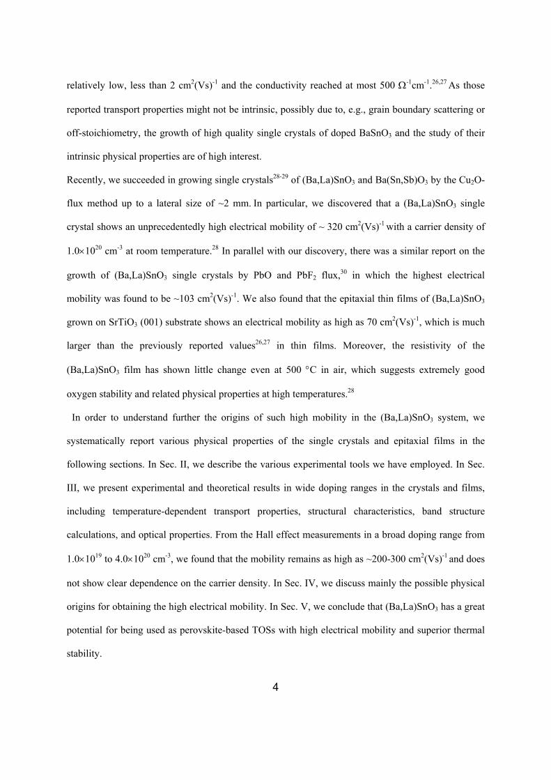
Figure 1 (c) shows the XRD pattern (θ-2θ scan) of a typical (Ba,La)SnO3 single crystal after
grinding into a fine powder form. The pattern reveals that the single crystal forms the cubic perovskite
phase without any detectable impurity phase. We have indeed tried to grow high quality single
crystals by using various kinds of fluxes to investigate the intrinsic properties of La-doped BaSnO3.
Among those trials, we could also grow rather a large size BaSnO3 single crystals (~221 mm3) by
using the mixed flux of PbO and PbF2, which is similar to the recent report.30 However, the EPMA
(electron-probe-micro-analyses) study28 showed that the grown single crystals using the Pb-containing
flux unavoidably contained significant Pb impurities. On the other hand, the crystals grown by the
Cu2O flux did not contain any Cu related impurity according to the EPMA study. It is thus expected
that our single crystals without any Cu impurity from the Cu2O flux can offer a better chance to
observe the intrinsic properties of (Ba,La)SnO3.
In the case of (Ba,La)SnO3 thin films, the XRD patterns in Fig. 1 (d) show the (00l) peaks, due to the
epitaxial growth on SrTiO3 (001) as demonstrated in the reciprocal mapping study in Ref. 28. The
inset in Fig. 1 (d) shows that the full-width-at-half-maximum (FWHM) in the rocking curve is only

8
0.09˚, supporting a high degree of crystallinity in our epitaxial film. It is worth mentioning that the
FWHM in a previous report was about 0.57˚,26 which is much larger than that of our films. This
experimental result suggests that the quality of the thin films should be superior to those studied in
previous publications.26,27
Figure 2 shows the variation of the lattice parameters of polycrystalline Ba1-xLaxSnO3 (x = 0.00, 0.01,
0.02, and 0.04) as obtained from the Rietveld refinement of the powder diffraction data. It is noted
that as the La concentration (x) increases, the lattice parameter increases almost linearly. It is rather
unusual to find such an increase of the lattice parameter while doping by the La3+ ion, which has a
smaller ionic radius (0.103 nm) than that of Ba2+ (0.135 nm).36 We will discuss the origin of this
unusual lattice expansion in a coming section B below.
B. First-principles calculations
Figure 3 presents the band structures of both BaSnO3 and (Ba,La)SnO3 as obtained by first-
principles density functional theory (DFT) calculations with local density approximation (LDA). To
our knowledge, the band structure calculation based on the LDA approximation was reported only for
BaSnO3,22 not for (Ba,La)SnO3. The band structures of BaSnO3 and (Ba,La)SnO3 were drawn for the
333 supercell with 27 unit cells corresponding to the doping rate of x = 0.037 in Ba1-xLaxSnO3.
According to the folded Brillouin zone of the 333 supercell as shown in Fig. 3 (a), BaSnO3 seems
to have an indirect band gap. Moreover, based on the band structure in Fig. 3 (b), the La-doping
provides electron states directly well-inside the conduction band of BaSnO3, which is mainly
characterized as the Sn 5s states with the Sn-O antibonding character. This means that a La ion acts as
an electron donor and its ionic valence becomes La3+. The occupation in the anti-bonding state is
likely to result in repulsive forces between Sn and O to lower the total energy of the crystal structure,
thereby inducing expansion of the lattice. The theoretically calculated equilibrium lattice constants of
BaSnO3 and 3.7% La doped BaSnO3 are found to be 4.098 Å and 4.102 Å, respectively, showing

9
clearly the increasing trend upon La doping, consistent with experimental results. This theoretical
result supports that the experimentally found lattice expansion upon La doping comes from the anti-
bonding nature of conduction bands.
It is further noted that the electronic structure of BaSnO3 has a highly dispersive conduction band,
mainly composed of Sn 5s bands, mainly due to the presence of an ideal Sn-O-Sn network with its
bonding angle close to 180.22 The shape of the conduction band is indeed similar to the LDA result
of the In2O337, a mother compound of the well-known TCO material, In2O3:Sn. This observation
indicates that similar to In2O3:Sn, there is a good possibility of obtaining highly mobile n-type carriers
in BaSnO3 upon doping. When the La doping is made to form (Ba,La)SnO3, the Fermi level is formed
well inside the Sn 5s band (the dotted line in Fig. 3 (b)). The change of the band structure by La-
doping is negligible near the Fermi level. The presence of La 4f bands at 2 eV above the Fermi level
did not affect the band dispersion of the original conduction band of BaSnO3. The calculated effective
masses of the conduction band turn out to be about 0.4m0 for both BaSnO3 and (Ba,La)SnO3, where
m0 is the free electron mass. The Fermi level of (Ba,La)SnO3 in Fig. 3 (b) indicates that the 3.7 % La
doped (Ba,La)SnO3 is in a degenerately doped regime with n-type carriers, which is consistent with
the temperature-dependent transport results explained below.
C. Transport properties
Figure 4 summarizes the resistivity and mobility variation as a function of carrier density at room
temperature in both single crystals and thin films. The data from our earlier report are also compared
(closed squares and triangles). Previously,28 we found that the mobility of single crystals is roughly
proportional to n-1, while the mobility of thin films is proportional to n1/2 in a low doping range
smaller than n = 41020 cm-3. The n-1 dependence of single crystals could be understood as an ionized-
dopant scattering effect, which is known to be roughly proportional to the number of scattering
centers, i.e., ionized dopant density.28 In the case of films, the n1/2 dependence could be mainly

10
attributed to the dominant dislocation or grain boundary scattering effects, which are increasingly
screened in roughly proportional to the square root of the mobile carrier density. The existence of the
dislocations or grain boundaries in the films is expected due to the large lattice mismatch between
(Ba,La)SnO3 and SrTiO3.
On the other hand, in the extended measurements for the single crystals in a broad doping range
from 1.01019 to 4.01020 cm-3, we find that the measured electrical mobility values are instead
scattered between 200 - 300 cm2(Vs)-1 without showing clear dependence on the carrier density. It is
noteworthy that the previous data for the single crystals (solid squares in Fig 4.) show rather large
variation of mobility and reduced mobility at a high carrier density although the crystals come from
the same batch. Thus, we tentatively presume that the crystals studied in Ref. 28 might have
systematic increase of oxygen vacancy with carrier density increase. We note that the present newly
updated mobility values still mark the highest record among the wide-band-gap oxide semiconductors
in a similar doping level; e.g., highest mobility around the doping level of n = ~ 11020 cm-3 was ~160
cm2(Vs)-1 for indium oxide (In2O3),38 ~ 50 cm2(Vs)-1 for tin oxide (SnO2),
39 and ~100 cm2(Vs)-1 for
zinc oxide (ZnO).40 We further note that, due to the high mobility of the (Ba,La)SnO3 system, the
conductivity value in the high doping regions above n = 21020 cm-3 is ~104 cm-1 in the single
crystal at room temperature (Fig. 4 (a)), which is close to the highest value among the transparent
conductors. The best conductivity of the In2O3:Sn is known to be ~104 cm-1. Thus, (Ba,La)SnO3
can be also used as transparent conductors.
To understand further detailed electrical transport properties, we performed the temperature-
dependent resistivity measurements as summarized in Fig. 5. First, we note that the carrier densities
are almost temperature-independent in both single crystals and films (Figs. 5 (a) and (b)). The
resistivities of both single crystals and films mostly increase as increasing temperature (Figs. 5 (e) and
(f)). The positive temperature coefficient of the resistivity and temperature-independent carrier
density clearly show the metallic behavior in both films and single crystals, indicating that all the

11
materials are in a degenerately doped semiconducting regime. The resistivity values of the single
crystals decrease nearly by a factor of two upon being cooled from room temperature to 2 K (Fig. 5
(e)), which then results in the increase of the corresponding mobility by the same factor (Fig. 5 (c)).
The mobility increases at low temperatures seem to be a common property of both crystals and films.
The factor of the resistivity decrease from room temperature to 2 K, as observed in the films with x =
0.04 and 0.07, is also reflected in the increase in the corresponding mobility (Fig. 5 (d)). On the other
hand, it is found that the residual resistivity values of the films are generally larger than those of the
crystals (Fig. 5 (f)) upon being compared at a similar carrier concentration (e.g. one order higher near
n 11020 cm-3), implying that there exist extra-scattering sources in the films such as grain
boundaries and dislocations.
D. Optical properties
Figure 6 compares the transmission and optical absorption spectra for the two single crystals,
undoped BaSnO3 and (Ba,La)SnO3 with n = 2.391020 cm-3. Transmittance of the BaSnO3 single
crystal reaches as high as 0.71 in the visible spectral region (1.8-3.1 eV) although its thickness of 68.7
m is rather high. The significant suppression of the transmittance as well as a sharp increase in
near 3.1 eV reflects the development of an optical gap. Transmittance of the La doped crystal is
progressively suppressed at a low frequency region, resulting in the Drude-type absorption tail,
presumbably due to the increase of free carriers. However, the transmittance level in the doped crystal
remains finite around 0.2 albeit it is rather thick (~53.7 m) and has rather a high doping level (n =
2.391020 cm-3). The resultant spectra of the doped crystal is still less than 300 cm-1 in the visible
spectral region, predicting that the doped sample should have transmittance of ~ 0.8 in e.g., a thin film
having thickness about 100 nm. This high transparency has been also observed in previous optical
studies on the thin films grown on SrTiO3 substrates26. It is also noted that the steeply increasing

12
part in has slightly shifted to a higher energy in the doped crystal, indicating the presence of the
Burstein-Moss shift41,42 as often observed in degenerate semiconductors.
According to the band calculation in Fig. 3, BaSnO3 is an indirect gap semiconductor, in which the
conduction band minimum and the valence band maximum have predominant Sn 5s and O 2p
characters, respectively. To determine experimentally the gap nature of BaSnO3, we plotted the curves
of α0.5 and α2 vs photon energy for both undoped BaSnO3 and (Ba,La)SnO3 in the inset of Fig. 6 (b).
For BaSnO3, we could find a linearly increasing region in both curves. Upon applying a linear
extrapolation, the indirect and direct band gaps are estimated as 2.95 eV and 3.10 eV, respectively.
This observation suggests that the optical transition with the lowest energy reflects the indirect
transition nature while the direct optical transition with a bit higher energy is quite strong in this
material. This is somewhat expected because the direct optical transition between the -points of the
valence and conduction band satisfies an optical selection rule (from O 2p to Sn 5s), while the indirect
transition from the valence band maximum (R-point) to the conduction band minimum (-point) are
generally low. It is noteworthy that quite similar optical transition characters have been also observed
in another cubic perovskite SrGeO3, a new TCO candidate compound reported recently.43
The experimentally estimated direct or indirect band gaps (2.95-3.10 eV) in BaSnO3 is much larger
than that (~1 eV) estimated from the band structure in Fig. 3. It is rather well-known that the gap
predicted by the band calculation based on the LDA approximation underestimates the actual gap in
many transparent oxide materials because the LDA calculation doesn’t take into account the electron
correlation effect properly. Even the well-known TCO, In2O3:Sn exhibits a similar kind of
discrepancy between the LDA calculation and the experimentally determined gap due to the
correlation effect37. In addition, In2O3:Sn was found to show yet another discrepancy of 0.81 eV
between the experimental optical gap and the gap measured by the photoemission and X-ray emission
spectroscopy due to the presence of the optical selection rule.44 Therefore, it will be interesting to
study in future the origin of such an optical gap enhancement in BaSnO3 as well. In reference to the

13
case of In2O3:Sn, it will be worthwhile to check whether the electron correlation effects alone can
explain the discrepancy or an additional optical selection becomes necessary.
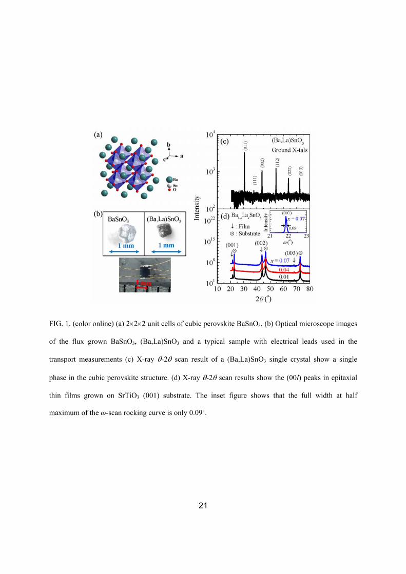
E. Debye temperatures
To extract the information on the Debye temperature, we used two methods, i.e., heat capacity and
thermal expansion measurements. Figure 7 (a) shows the specific heat of a BaSnO3 single crystal at
temperatures between 2 and 330 K. For the heat capacity analysis, we found that the two Debye
phonon modes become necessary because one phonon mode alone could not fully explain the
experimental data. Based on the Debye theory, the temperature dependent specific heat coming from
the two phonon contributions can be described as follows:45
9⁄
d⁄
d (1)
, where low and high are the Debye temperatures of each phonon mode, and x and y are the weights
of the phonon modes. Open circles represent the temperature-dependent specific heat data of the
BaSnO3 single crystal while the lines refer to the two phonon mode contributions (dotted lines) and
their sum (solid line). The model fitting can successfully explain the experimental data at least above
20 K and the resultant two Debye temperatures low and high are found to be 307 K and 950 K,
respectively. The resultant x/y ratio is around 1.5, implying that the heat capacity below 300 K is
mainly governed by the low energy Debye phonon.
Figure 7 (b) displays the evolution of temperature-dependent lattice constant of a Ba0.999La0.001SnO3
polycrystalline specimen. Upon increasing the temperature, the lattice parameter increases, consistent
with lattice expansion due to anharmonic thermal vibration. To model the thermal expansion data of
Ba0.999La0.001SnO3, we assumed that the two Debye temperatures as obtained from the heat capacity
data can explain the intrinsic energy of the lattice and thus its temperature-dependent expansion as
well. Then, the temperature dependencies of the lattice parameter (a) can be described as:46
⁄d
⁄d (2)

14
, where a0 and D are the lattice constant at 0 K and Debye temperature, respectively, and b and c
are the constant prefactors. Upon using the same Debye temperatures from heat capacity, we could get
satisfactory fitting result, confirming that the two Debye temperatures of 307 K and 950 K are quite
effective in describing the lattice energy and related thermal properties. As the two Debye
temperatures are quite different, one phonon mode around 300 K seems to be approximately effective
in describing the phonon properties of BaSnO3 at low temperatures. For example, upon fitting the
thermal expansion data with one Debye temperature of 365 K, we could obtain almost the same good
fit results as the two phonon approximation (not shown), supporting that the lower energy phonon
mode contributes mostly the thermal expansion as well.
IV. DISCUSSION
The electrical mobility () in a simple one band model is expressed by an electron effective mass
(m*) and a total electron scattering rate (-1):
/ , (3)
where e is an electron charge. Therefore, a high mobility can be realized with a small electron
effective mass and a small total electron scattering rate. In the followings, we discuss the origins for
achieving such a high mobility in (Ba,La)SnO3 based on the peculiar characteristics reflected in the
two key physical parameters, i.e., electron scattering rate and effective mass.
A. High mobility in the crystals and thin films
Controlling impurity scattering seems to be important to obtain the highest mobility of ~ 320
cm2(Vs)-1 in (Ba,La)SnO3 single crystals as observed in our previous study28 and 200- 300 cm2(Vs)-1
as found in this work. It was recently reported that single crystals grown by PbO + PbF2 flux
produced a mobility30 close to 103 cm2(Vs)-1 at a doping level ~ 8 – 101019 cm-3. As the Pb impurity
can enter both Ba and Sn sites in this flux, the observation of lower mobility implies that the presence

15
of the additional impurity other than La might lead to the increased dopant scattering. As mentioned
in Sec. III A, the absence of Cu impurity in our single crystals should be then helpful in reducing the
additional impurity scattering and obtaining physical properties close to the intrinsic ones.
In the thin films, it is interesting to note that a previous study found the mobility to be at best 0.69
cm2(Vs)-1 although the reported (Ba,La)SnO3 films were epitaxially grown on the same type of
substrate, SrTiO3 (001),26 as the present work. The FWHM in the rocking curve was 0.57 in the
previous study26 while it is 0.09 in our study (Fig. 1 (d)), which represents a conspicuous
improvement in the crystallinity. Therefore, the highest electrical mobility of ~ 70 cm2(Vs)-1 realized
in our thin films is most likely to be associated with the superior structural properties.
On the other hand, the highest mobility of ~ 70 cm2(Vs)-1 in our films is still much lower than the
values in the single crystals. Even though our films were epitaxially grown, we found from the
transmission electron microscopy study that there exist significant grain boundaries and threading
dislocations, due to the large lattice mismatch (more than 4%) between the substrate and (Ba,La)SnO3.
Those grain boundaries/dislocations are expected to act as double-Schotttky barriers for the electron
transport,47,48 thereby giving rise to lower electrical mobility and higher residual resistivity than single
crystals as demonstrated in Fig. 5. Therefore, it is expected that the mobility in thin films will be
further improved when the dislocation density gets reduced by, e.g., using BaSnO3 single crystal
substrates.
Related to the presence of such grain boundaries/dislocations, the room temperature carrier densities
in the films with nominal doping concentration x = 0.01, 0.04, and 0.07 are 7.01019 cm-3, 4.01020
cm-3, and 6.81020 cm-3, respectively. The activation rates of dopants then become 45, 69, and 67 %,
respectively. The lower activation rate for the lowest doping indicates existence of the enhanced
charge trapping mechanism. Moreover, as evident in Fig. 5 (d), the mobility is reduced significantly
when carrier density is decreased.28 This observation implies that the higher carrier density effectively
reduces the effect of dislocation/grain boundary scattering. Once the double Schottky barrier is

16
formed in the films, the higher carrier density is likely to induce thinner barrier width and smear out
the barriers, resulting in the enhanced mobility as the carrier density increases up to around n ~ 41020
cm−3. However, as the doping rate becomes higher than 41020 cm-3, the scattering by ionized dopants
seems to start dominating rather than dislocations or grain boundaries, to induce a mobility decrease
by the increased dopant level.
B. Effective mass
To understand the high mobility observed in the (Ba,La)SnO3 single crystals within the band
structure framework, one should expect quite a small effective mass. As mentioned in the LDA
calculation results (Sec. III B), the effective masses of BaSnO3 and (Ba,La)SnO3 are predicted to be
~0.4m0. It turns out that the value of ~0.4m0 is comparable to, but not particularly smaller than the
theoretically predicted effective masses of other wide-band-gap oxide semiconductors, e.g., In2O3
(0.30m0),49 SnO2 (0.38m0),
50 and ZnO (0.24m0).51 The effective mass can be also estimated by the
Burstein-Moss shift,41,42 which predicts the energy difference in the optical band gap (ΔE) between
undoped and doped semiconductors as ΔE = h2(3n/π) 2/3/(8m*), where h is Plank constant and m* is
effective mass. As we estimate ΔE from the shift in the direct optical gap in the inset of Fig. 6 b, ΔE =
~ 0.23 eV so that the effective mass is estimated as ~ 0.60m0. This value is slightly larger than the
theoretical prediction but small enough to guarantee a high mobility. On the other hand, there exist
another recent predictions of m* =0.06m052 or 0.2m0
53 based on the LDA calculations based on
different approximations such as GGA (generalized gradient approximation) or use of a specific
hybid-functional, respectively. The predictions of the effective mass at this stage are thus scattered,
ranging from 0.06 to 0.5m0, indicating that it is rather sensitive to the approximation in the DFT
calculation. Therefore, to pin down whether the effective mass is a dominant quantity for creating the
high mobility or not, it would be necessary to determine an effective mass of (Ba,La)SnO3 more
accurately.

17
C. Effects of various scattering in the crystal
Another key physical quantity to determine the electrical mobility is the electron scattering rate,
which can be expressed by a sum of several scattering rates, according to Matthiessen's rule:
∑ (4)
, where are the electron scattering rates from different scattering sources. In the single crystals of
(Ba,La)SnO3 with minimized extrinsic scattering sources, e.g., defects, the electron-phonon and
ionized-dopant scatterings are likely to be main sources of the electron scattering. It is generally
known that the ionized-dopant scattering in the degenerately doped regime is almost temperature
independent. Then, the majority of the temperature-dependent scattering can be attributed to the
electron-phonon scattering in the (Ba,La)SnO3 system, in which the degenerately doped regime is
clearly realized when the doping rate is higher than 1.01019 cm-3. For example, the temperature-
dependent resistivity variation should be then determined by the electron-phonon scattering as the
carrier density is mostly temperature-independent (Fig. 4 (b)).
The Debye temperature should be closely related to the electron-phonon scattering strength, as the
electron-phonon scattering will increase with the number of thermally activated phonons; e.g., a
smaller Debye temperature will result in a higher amount of phonon population at a given temperature.
The Debye temperatures of (Ba,La)SnO3 are 307 K and 950 K as determined by both heat capacity
and thermal expansion measurements. The Debye temperature of 307 K is indeed a bit lower than the
known Debye temperatures of In2O3 (420 K),54 SnO2 (500 K),54 and, ZnO (399.5 K).55 Therefore, it is
expected that the electron-phonon scattering in (Ba,La)SnO3 should not be particularly smaller to
cause the higher mobility than those of the other transparent electronic materials.
Another important contribution to the total scattering rate is the ionized-dopant scattering. In
(Ba,La)SnO3, the La3+ dopants are the main ionized impurities. In a degenerately doped
semiconductor, the mobility due to the ionized impurity (ii) can be expressed as:56,57

18
Z and 3π /
/ (5)
, where the screening function Fii(d) is given by:
1 1 ln 1 2 1 and 1 . (6)
Here, h is Planck’s constant, Ni is a number of ionized dopant, and r is a dielectric constant. is
the effective mass at the conduction band edge and 1 2 C , where α is the non-
parabolicity parameter and E EC is the electron energy relative to the conduction band edge (EC).
Equation (5) predicts that in the ionized impurity scattering regime, ii is generally proportional to the
square of the dielectric constant. We should note that the dielectric constant of BaSnO3 (about 20)58 is
almost two times larger than the well-known transparent electronic materials; In2O3 (about 9), SnO2
(9.6 - 13.5), and ZnO (8.75 - 7.8).56 Therefore, the high mobility state in (Ba,La)SnO3 may be due to
greatly reduced ionized-dopant scattering, coming from the enhanced screening strength associated
with the high dielectric constant.
Another important factor to reduce the ionized-dopant scattering could be the capability of doping
the La dopant into the Ba site. It is expected that the ionized-dopant scattering should be greatly
reduced if the dopant is located away from the SnO2 network that are the main conduction paths. This
would be favorable for realizing almost defect-free SnO2 conduction paths. Empirical comparison of
the residual resistivity supports this reasoning. The residual resistivity of the Ta doped SnO2 was ~
0.83 mcm, at n = ~ 11020 cm-3,39 which is seven times larger than that of (Ba,La)SnO3 single
crystal, ~ 0.12 mcm at n = 1.181020 cm-3 (Fig. 5). Thus, it is postulated that the location of La
dopant away from the SnO2 conduction paths plays an important role to minimize the ionized-dopant
scattering as well.
One caveat in applying equation (5) to understand the ionized-dopant scattering in our single crystals
lies in the screening function Fii(d). Once the ionized impurity level (Ni) and actual carrier density (n)
are proportional to each other, ii is inversely proportional to Fii(d). In general, Fii(d) increases as the

19
carrier density increases so that one should expect a reduced ii with increase of n in the ionized-
dopant scattering regime. However, the new result in Fig. 4 (b) is not yet decisive to draw a
conclusion whether the mobility indeed shows any dependence on n. The mobility values near the
same carrier density level exhibit large scatter. This indicates that the single crystals are not yet
perfect so that they might have additional scattering sources such as oxygen vacancies. If the oxygen
vacancies are present in the middle of the SnO2 conduction paths, they are expected to act as stronger
scattering centers than the La3+ ions. Moreover, the actual carrier density can be also fluctuating inside
a single crystal or over different pieces, possibly resulting in the scattered mobility and carrier density
as seen in Fig. 4 (b). In light of the very small oxygen diffusion constant in BaSnO3 material system,
as we reported previously,28 full and uniform oxygenation of mm-thick crystals may be difficult.
Further studies are underway to reduce such additional scattering sources.
V. CONCLUSIONS
We found a high electrical mobility in the transparent perovskite material, (Ba,La)SnO3. The
(Ba,La)SnO3 single crystals grown by the Cu2O flux method showed an electrical mobility of 200-300
cm2(Vs)-1 in a broad doping range from 1.01019 to 4.01020 cm-3, constituting the highest value
among the known transparent electronic materials, such as doped In2O3, SnO2, and ZnO. In the thin
films grown epitaxially on SrTiO3 (001), the maximum mobility reached only ~ 70 cm2(Vs)-1 due to
the presence of dislocations/grain boundaries, which points out the possibility of enhancing the
mobility in the thin film form upon having a proper substrate material. We discussed that the high
mobility can arise from several unique physical conditions of (Ba,La)SnO3: highly dispersive Sn 5s
band coming from an ideal Sn-O-Sn bonding angle close to 180 and minimized ionized-dopant
scattering from the high dielectric constant and the capability of putting La3+ dopant away from the
main SnO2 conduction paths. Moreover, it is noteworthy that such a high mobility is linked to the high
conductivity ~ 104 -1cm-1 at room temperature at a doping level of n = 21020 cm-3, which is

20
comparable to the highest value among the transparent conducting oxides. Therefore, combined with
the thermal stability of the oxygen diffusion, the (Ba,La)SnO3 system offers an unprecedented
opportunity for realizing all perovskite based, transparent high-temperature, high-power functional
devices.
ACKNOWLEDGEMENTS
We thank Tae Won Noh, Yun Daniel Park, and Tak Hee Lee for discussions. We acknowledge
support from the NRF through Accelerated Research Program (R17-2008-33-01000-0) and through
the Creative Research Initiative (2010-0018300), and by MKE through the Fundamental R&D
program for Core Technology of Materials.
†Correspondence and requests for materials should be addressed to Kee Hoon Kim ([email protected]) and Kookrin Char ([email protected]).
21
FIG. 1. (color online) (a) 222 unit cells of cubic perovskite BaSnO3. (b) Optical microscope images
of the flux grown BaSnO3, (Ba,La)SnO3 and a typical sample with electrical leads used in the
transport measurements (c) X-ray -2 scan result of a (Ba,La)SnO3 single crystal show a single
phase in the cubic perovskite structure. (d) X-ray -2 scan results show the (00l) peaks in epitaxial
thin films grown on SrTiO3 (001) substrate. The inset figure shows that the full width at half
maximum of the ω-scan rocking curve is only 0.09˚.

22
FIG. 2. (a) Cubic lattice parameter for polycrystalline Ba1-xLaxSnO3 (x = 0, 0.01, 0.02, and 0.04)
measured at RT. Line is drawn as a guide to the eye.

23
FIG 3. The band structure of (a) BaSnO3 and (b) (Ba,La)SnO3 obtained by first-principles calculations
with 27 (333) unit cells. For (Ba,La)SnO3, one of Ba2+ ions is substituted by a La3+ ion
corresponding to the doping rate of x=0.037 in Ba1-xLaxSnO3.

24
FIG. 4. (color online) (a) Resistivity () and (b) mobility () vs. carrier density (n) plot. closed (black)
squares and (green) triangles are for the reported single crystals and films28, respectively. Closed (red)
circles are for the data of single crystals in this work.

25
FIG. 5. (color online) Temperature-dependent carrier density n, resistivity , and mobility are
plotted for selected (Ba,La)SnO3 single crystals (BLSO #1, 2, 3, and 4) (a,c,e) and thin films (b,d,f).
The nominal La composition (x) is presented for the thin films.

26
FIG. 6. (color online) (a) Transmission spectra and (b) absorption coefficient () of BaSnO3 (BSO)
and (Ba,La)SnO3 single crystals are plotted as a function of photon energy. Absorption coefficient
for each undoped and doped sample (n = 2.391020 cm-3) was extracted by measurements of
transmission spectra of the same specimen in two different thicknesses. The inset shows that the
curves of α0.5 and α2 vs photon energy for both undoped BaSnO3 and (Ba,La)SnO3.
27
Fig. 7 (color online) (a) Open circles are the temperature dependent specific heat of BaSnO3 single
crystal. The dotted lines are two phonon mode contributions (blue and green) and the solid line refers
to their sum (red). (b) Thermally induced cubic lattice parameter expansion of polycrystalline
Ba0.999La0.001SnO3. The solid (red) line is the thermal expansion fitting based on the Debye model with
the two Debye temperatures.

28
REFERENCES
1. D. S. Ginley and C. Bright, MRS Bull. 25, 15 (2000).
2. A. J. Freeman, K. R. Poeppelmeier, T. O. Mason, R. P. H. Chang, and T. J. Marks, MRS Bull. 25,
45 (2000).
3. T. Minami, MRS Bull. 25, 38 (2000).
4. H. Hosono, Thin Solid Films 515, 6000 (2007).
5. Z. K. Tang, G. K. L. Wong, P. Yu, M. Kawasaki, A. Ohtomo, H. Koinuma, and Y. Segawa, Appl.
Phys. Lett. 72, 3270 (1998).
6. H. Ohta, M. Orita, M. Hirano, H. Tanji, H. Kawazoe, and H. Hosono, Appl. Phys. Lett. 76, 2740
(2000).
7. T. Makino, Y. Segawa, A. Tsukazaki, A. Ohtomo, and M. Kawasaki, Appl. Phys. Lett. 87, 022101
(2005).
8. K. Nomura, H. Ohta, K. Ueda, T. Kamiya, M. Hirano, and H. Hosono, Science 300, 1269 (2003)
9. R. J. Cava, B. Batlogg, J. J. Krajewski, R. Farrow, L. W. Rupp Jr, A. E. White, K. Short, W. F.
Peck, and T. Kometani , Nature 332, 814 (1988).
10. Y. Tokura and Y. Tomioka, J. Magn. Magn. Mater. 200, 1 (1999).
11. G. H. Haertling, J. Am. Ceram. Soc. 82, 797 (1999).
12. T. Kimura, T. Goto, H. Shintani, K. Ishizaka, T. Arima, and Y. Tokura, Nature 426, 55 (2003).
13. C. H. Ahn, J.-M. Triscone, and J. Mannhart, Nature 424, 1015 (2003).
14. H.-H. Wang, D.-F. Cui, S.-Y Dai, H.-B. Lu, Y.-L. Zhou, Z.-H. Chen, and G.-Z. Yang, J. Appl.
Phys. 90, 4664 (2001).
15. H. Guo, L. Liu, Y. Fei, W. Xiang, H. Lü, S. Dai, Y. Zhou, and Z. Chen, J. Appl. Phys. 94, 4558
(2003).
16. J. H. Cho and H. J. Cho, Appl. Phys. Lett.79, 1426 (2001).
17. R. P. Wang and C. J. Tao, J. Crys. Growth 245, 63 (2002).

29
18. K. Ueda, H. Yanagi, H. Hosono, and H. Kawazoe, Phys. Rev. B 56, 12998 (1997).
19. B. Hadjarab, A. Bouguelia, and M. Trari, J. Phys. Chem. Solids 68, 1491 (2007).
20. P. Singh, D. Kumar, and O. Parkash, J. Appl. Phys. 97, 074103 (2005).
21. U. Lampe, J. Gerblinger, and H. Meixner, Sens. Actuators, B, 24-25, 657 (1995).
22. H. Mizoguchi, H. W. Eng, and P. M. Woodward, Inorg. Chem. 43, 1667 (2004).
23. T. Huang, T. Nakamura, M. Itoh, Y. Inaguma, and O. Ishiyama, J. Mater. Sci. 30, 1556 (1995).
24. R. J. Cava, P. Gammel, B. Batlogg, J. J. Krajewski, W. F. Peck, Jr., L. W. Rupp, Jr., R. Felder,
and R. B. van Dover, Phys. Rev. B 42, 4815 (1990).
25. M. Yasukawa, T. Kono, K. Ueda, H. Yanagi, H. Hosono, Mater. Sci. Eng. B. 173, 29 (2010).
26. H. F. Wang, Q. Z. Liu, F. Chen, G. Y. Gao, W. Wu, and X. H. Chen, J. Appl. Phys. 101, 106105
(2007).
27. Q. Liu, J. Dai, Z. Liu, X. Zhang, G. Zhu, and G. Ding, J. Phys. D: Appl. Phys. 43, 455401 (2010).
28. H. J. Kim, U. Kim , H. M. Kim, T. H. Kim, H. S. Mun, B.-G. Jeon, K. T. Hong, W.-J. Lee, C. Ju,
K. H. Kim, and K. Char, Appl. Phys. Express 5, 061102 (2012).
29. H. J. Kim, J. Kim, W. S. Choi, D. W. Jeong, J. Yu, T. W. Noh, and K. H. Kim, 2012 MRS Spring
Meeting & Exhibit G9.12/S8.12
30. X. Luo, Y. S. Oh, A. Sirenko, P. Gao, T. A. Tyson, K. Char, and S.-W. Cheong, Appl. Phys. Lett.
100, 172112 (2012).
31. G.Kresse and J. Furthmüller, Phys. Rev. B 54, 11169 (1996).
32. P. E. Blöchl, Phys. Rev. B 50, 17953 (1994).
33. D. M. Ceperley and B. J. Alder, Phys. Rev. Lett. 45, 566 (1980).
34. R. Bachmann, F. J. DiSalvo, Jr., T. H. Geballe, R. L. Greene, R. E. Howard, C. N. King, H. C.
Kirsch, K. N. Lee, R. E. Schwall, H.‐U. Thomas, and R. B. Zubeck, Rev. Sci. Instrum. 43, 205
(1972).
35. J. S. Hwang, K. J. Lin, and C. Tien, Rev. Sci. Instrum. 68, 94 (1997).

30
36. R. D. Shannon, Acta Cryst. A 32, 751 (1976).
37. O. N. Mryasov and A. J. Freeman, Phys. Rev. B 64, 233111 (2001).
38. R. L. Weiher, J. Appl. Phys. 33, 2834 (1962).
39. H. Toyosaki, M. Kawasaki, and Y. Tokura, Appl. Phys. Lett. 93, 132109 (2008).
40. A. Ohtomo, K. Tamura, K. Saikusa, K. Takahashi, T. Makino, Y. Segawa, H. Koinuma, and M.
Kawasaki, Appl. Phys. Lett. 75, 2635 (1999).
41. E. Burstein, Phys, Rev. 93, 632 (1954).
42. T. S. Moss, Proc. Phys. Soc. (London) B67, 775 (1954).
43. H. Mizoguchi, T. Kamiya, S. Matsuishi, and H. Hosono, Nature Comm. 2, 470 (2011).
44. A. Walsh, J. L. F. Da Silva, S.-H. Wei, C. Körber, A. Klein, L. F. J. Piper, A. DeMasi, K. E.
Smith, G. Panaccione, P. Torelli, D. J. Payne, A. Bourlange, and R. G. Egdell, Phys. Rev. Lett.
100, 167402 (2008).
45. A. D. Fortes, I. G. Wood, J. P. Brodholt, M. Alfredsson, L. Vočadlo, G. S. McGrady, and K. S.
Knight, J. Chem. Phys. 119, 10806 (2003).
46. C. Roder, S. Einfeldt, S. Figge, and D. Hommel. Phys. Rev. B 72, 085218 (2005).
47. M. Vollman and R. Waser, J. Am. Ceram. Soc. 77, 235 (1994).
48. K. Ellmer and R. Mientus, Thin Solid Films 516, 4620 (2008).
49. H. Odaka, S. Iwata, N. Taga, S. Ohnishi, Y. Kaneta, and Y.Shigesato, Jpn. J. Appl. Phys. 36, 5551
(1997).
50. P. D. Borges, L. M. R. Scolfaro, H. W. L. Alves and E. F. da Silva, Jr., Theor. Chem. Acc. 126, 39
(2010).
51. M. Oshikiri, Y. Imanaka, F. Aryasetiawan, and G. Kido, Physica B 298, 472 (2001).
52. E. Moreira, J. M. Henriques, D. L. Azevedo, E. W. S. Caetano, V. N. Freire, and E. L.
Albuquerque, J. Solid State Chem. 187, 186 (2012).
53. H.-R Liu, J.-H. Yang, H. J. Xiang, X. G. Gong, and Su-Huai Wei, arXiv:1209.2845
54. K. J. Bachmann, F.S.L. Hsu, and J. P. Remeika, Phys. Stat. Sol. (a) 67, K39 (1981).

31
55. W. N. Lawless and T. K. Gupta, J. Appl. Phys. 60, 607 (1986).
56. K. Ellmer, J. Phys. D: Appl. Phys. 34 3097 (2001).
57. T. Pisarkiewicz, K. Zakrzewska and E. Leja, Thin Solid Films 174, 217 (1989).
58. P. Singh, B. J. Brandenburg, C. P. Sebastian, P. Singh, S. Singh, D. Kumar, and O. Parkash, Jpn. J.
Appl. Phys. 47, 3540 (2008).