Embed Size (px)
Citation preview
PHYSICAL REVIEW B 102, 035125 (2020)Editors’ Suggestion
Eightfold fermionic excitation in a charge density wave compound
Xi Zhang,1 Qiangqiang Gu,1 Haigen Sun,2 Tianchuang Luo ,1 Yanzhao Liu,1 Yueyuan Chen,1 Zhibin Shao,3
Zongyuan Zhang,2 Shaojian Li,2 Yuanwei Sun,1,4 Yuehui Li,1,4 Xiaokang Li,2,5 Shangjie Xue,1,6 Jun Ge,1 Ying Xing,7
R. Comin,6 Zengwei Zhu,2,5 Peng Gao,1,4,8 Binghai Yan,9 Ji Feng,1,10,* Minghu Pan ,2,3,† and Jian Wang 1,8,10,‡
1International Center for Quantum Materials, School of Physics, Peking University, Beijing 100871, China2School of Physics, Huazhong University of Science and Technology, Wuhan 430074, China
3School of Physics and Information Technology, Shaanxi Normal University, Xi’an 710062, China4Electron Microscopy Laboratory, School of Physics, Peking University, Beijing 100871, China
5Wuhan National High Magnetic Field Center, Huazhong University of Science and Technology, Wuhan 430074, China6Department of Physics, Massachusetts Institute of Technology, Cambridge, Massachusetts 02139, USA
7Department of Materials Science and Engineering, School of New Energy and Materials,China University of Petroleum, Beijing 102249, China
8Beijing Academy of Quantum Information Sciences, Beijing 100193, China9Department of Condensed Matter Physics, Weizmann Institute of Science, Rehovot 7610001, Israel
10CAS Center for Excellence in Topological Quantum Computation, University of Chinese Academy of Sciences, Beijing 100190, China
(Received 12 September 2019; accepted 24 June 2020; published 14 July 2020)
Unconventional quasiparticle excitations in condensed matter systems have become one of the most importantresearch frontiers. Beyond twofold and fourfold degenerate Weyl and Dirac fermions, threefold, sixfold, andeightfold symmetry protected degeneracies have been predicted. However they remain challenging to realize insolid state materials. Here the charge density wave compound TaTe4 is proposed to hold eightfold fermionicexcitation and Dirac point in energy bands. High quality TaTe4 single crystals are prepared, where the chargedensity wave is revealed by directly imaging the atomic structure and a pseudogap of about 45 meV on thesurface. Shubnikov-de Haas oscillations of TaTe4 are consistent with band structure calculation. Scanningtunneling microscopy/spectroscopy reveals atomic step edge states on the surface of TaTe4. This work uncoversthat the charge density wave is able to induce new topological phases and sheds new light on the novel excitationsin condensed matter materials.
DOI: 10.1103/PhysRevB.102.035125
I. INTRODUCTION
Condensed matter systems, as a translational symmetrybroken universe, host passionately pursued quasiparticle ex-citations analogous to high-energy elementary particles. Asuccessful example is the prediction and observation of Dirac[1–3] and Weyl [4–6] fermions in solids protected by bandtopology. Weyl semimetals (WSMs) hold twofold degenerateWeyl points with nontrivial Chern number in energy bands.Fourfold degenerate Dirac points (DPs) with linear dispersionprotected by time-reversal and inversion symmetry exist inDirac semimetals (DSMs) and are stabilized by uniaxial ro-tation symmetries [7] or nonsymmorphic space group (SG)symmetries [1]. Recently, relations between Dirac or Weylfermions and collective phenomena such as superconductivity(SC) is addressed [8–11], which is regarded as a route torealize topological SC and condensed matter analog of a thirdtype of elementary particle, Majorana fermions [12].
However, the marvelous story is to be continued. First,classification of condensed matter fermionic excitations by
*Corresponding author: [email protected]†Corresponding author: [email protected]‡Corresponding author: [email protected]
Dirac, Weyl, and Majorana is incomplete. The 230 SG sym-metries in three-dimensional (3D) lattices impose constraintsweaker than Poincaré symmetry required in quantum fieldtheory and therefore permit free fermionic excitations with nohigh-energy analog. Complete enumeration predicts threefold,sixfold, and eightfold degenerate fermions in condensed mat-ter systems in addition to Dirac and Weyl fermions [13,14].Threefold degeneracy has already been observed in MoP [15]and WC [16] while other types are still awaiting confirmationin real materials.
Second, apart from SC, another collective phenomenon ofparticular interest, the charge density wave (CDW), is muchless studied in the context of topological materials. CDW isthe ground state of a wide range of bulk compounds showingquasi-one-dimensional (quasi-1D) or quasi-two-dimensional(quasi-2D) lattice structures such as NbSe3 [17], (TaSe4)2I[18,19], and some transition metal dichalcogenides [20] aris-ing from electron-phonon interaction. When cooling belowPeierls transition temperature Tp, periodic modulation ofcharge density as well as structural distortion occur in thesematerials and an energy gap is opened at Fermi level. Similarto SC, CDW is also characterized by a complex order param-eter �eiϕ , where the phase ϕ is of fundamental importance,whose fluctuation forms a gapless current-carrying phasemode. However, the phase mode of the CDW can be pinned by
2469-9950/2020/102(3)/035125(8) 035125-1 ©2020 American Physical Society
XI ZHANG et al. PHYSICAL REVIEW B 102, 035125 (2020)
impurities, lattice defects, and, in the commensurate case, thelattice itself. As a result, they can only give rise to nonlinearconductivity above a threshold electric field ET [21].
Interplay between CDW and topology has been theoreti-cally considered in the context of 2D DSMs [22], topologicalinsulators (TIs) [23], topological WSMs [24,25], and DSMs[26]. In weak TI, the CDW is predicted to gap the surfacestates, however, create helical edge states on CDW domainwalls [23]. In WSMs and DSMs, interaction effect may inducethe CDW which gaps topologically protected degeneracypoints and the phase of the CDW couples to the electromag-netic field in an analogous way to axion [25,26]. However,up to now, experimental studies of the CDW in topologicalsemimetals are insufficient to test these hypotheses. Attemptsof identifying topological phases in typical CDW compoundsare also lacking.
In this article we report a topological semimetal phase ina CDW compound TaTe4. TaTe4 is structurally regarded asone of the simplest inorganic materials hosting a CDW [27].Our calculation further points out that TaTe4 is a topologicalsemimetal both with and without the presence of the CDW.In its undistorted crystal structure P4/mcc (SG124) withoutCDW, TaTe4 holds DPs along high symmetry lines �-Z andM-A. A commensurate CDW phase in TaTe4 is calculated tobe the zero-temperature ground state and hold double Diracpoint (DDP) with eightfold degeneracy at A as well as a Diracpoint at Z in the CDW Brillouin zone. The calculated bandstructure of the CDW phase is consistent with the observedShubnikov-de Haas (SdH) oscillations. The nontrivial topol-ogy of TaTe4 is also suggested by the scanning tunnelingspectroscopy (STS) detection of states residing on atomic stepedges on the surface of TaTe4. The coexistence of the CDWand fermionic excitations has been rarely reported before inother materials. Our results reveal the CDW-induced topolog-ical phases, which may lead to the possibility of dynamicallytuning the topological properties of crystalline materials, andprovide new insight into the interplay between the CDW andfermionic excitations.
II. EXPERIMENTAL AND CALCULATION METHODS
A. Band structure calculations
A density functional theory (DFT) calculation is performedusing Vienna ab initio simulation package (VASP) [28]within the generalized gradient approximation, parametrizedby Perdew, Burke, and Ernzerhof [29]. The energy cutoff for aplane-wave basis is set to 400 eV and the k-point mesh is takenas 11 × 11 × 11 for the non-CDW phase and 5 × 5 × 5 for theCDW phase. The CDW structure of TaTe4 is obtained by fullyrelaxing a 2a × 2b × 3c supercell of the non-CDW phase ofTaTe4 after adding a random distortion. a, b, and c are latticevectors in the non-CDW unit cell. The fully relaxation pro-cedure was performed with a conjugated gradient algorithm,until the Hellmann-Feynman force on each atom is less than10−3 eV/Å. The spin-orbit coupling effect is self-consistentlyincluded.
B. Single-crystal growth
High quality TaTe4 single crystals are prepared by chem-ical vapor transport (CVT) technique in a multizone single
crystal furnace [30]. Ta and Te powder are mixed at atomicratio 1:4.3 and sealed with 5 − 10 mg/cm3 iodine in anevacuated quartz tube. The mixture is first heated to 1000 °Cand kept for 12 h, and then slowly cooled down to roomtemperature. The quartz tube is then placed coaxially in themultizone furnace and the multizone function is used. Thereaction zone is kept at 540 °C and growth zone at 440 °C for7 days. After slowly cooling down to room temperature, bulksamples with metallic luster are obtained. Samples grown bythis method are quite stable in atmosphere.
C. Sample characterization and transport measurements
Chemical composition of prepared crystals is confirmed byenergy dispersive x-ray spectroscopy (EDS). The high-angleannular dark-field (HAADF) scanning transmission electronmicroscopy (STEM) image is performed on an aberration-corrected transmission electron microscope FEI Titan CubedThemis G2 300. The single crystal property of the sample isconfirmed by a Bruker D8 Advance powder x-ray diffractome-ter. ρ − T measurement and magnetotransport measurementunder magnetic field up to 15 T are performed in a PhysicalProperty Measurement System (PPMS-16 T) by QuantumDesign. Magnetoresistance up to 56 T is measured at WuhanNational High Magnetic Field Center with a pulsed magneticfield. Standard 4-probe/6-probe configuration is used through-out transport measurements.
D. Scanning tunneling microscopy (STM) measurements
For the STM study, the crystals chosen are approximatelythe size 2 mm × 1 mm×0.5 mm. Samples are first cleavedin situ at room temperature in an ultrahigh vacuum chamberwith pressure lower than 1 × 10⁻¹⁰ Torr. After cleavage, thecrystal exhibits a mirrorlike surface. An electrochemicallyetched tungsten wire is used as the STM tip. All measurementsby STM were conducted at liquid helium temperature 4.2 K.
III. RESULTS AND DISCUSSION
A. Crystal structure and schematic electronic structure of TaTe4
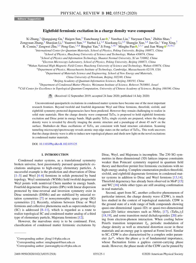
TaTe4 crystallizes in a tetragonal P4/mcc space group inthe absence of the CDW. Quasi-1D chains along the c axis areformed by every Ta surrounded by 8 Te atoms [Fig. 1(a)] (alsosee Fig. S1 in the Supplemental Material (SM) [31]). At roomtemperature, TaTe4 exhibits a commensurate CDW phase,which enlarges its unit cell to be 2a × 2b × 3c [Fig. 1(a)](also see SM [31] Fig. S2). With CDW distortion, Ta atomsform Ta3 clusters in the chain while Te atoms are slightlyrotated around the Ta chains, which develop the equivalent1D chains into three distinct types. The simulated CDW phasecrystal structure is consistent with previous [38,39] and ourexperimental observations. The space group under the CDWphase is P4/ncc where C4 rotation and inversion symmetryare preserved. We prepare TaTe4 single crystals using theCVT technique (details are presented in Methods section).The atomically resolved HAADF STEM image manifests thehigh quality of our sample [Fig. 2(a)]. Schematic structureclearly shows lattice distortions. After performing fast Fouriertransform (FFT), four spots around the center are detected to
035125-2
EIGHTFOLD FERMIONIC EXCITATION IN A CHARGE … PHYSICAL REVIEW B 102, 035125 (2020)
FIG. 1. Band structures of TaTe4 with and without CDW. (a) Lower left panel and right panel show unit cell of non-CDW phase and CDWphase TaTe4, where green polyhedrons indicate Ta3 clusters. Upper left panel is the 3D bulk Brillouin zone of non-CDW/CDW phase TaTe4
with high-symmetry points indicated. (b) Band structure along high-symmetry lines in the non-CDW Brillouin zone of TaTe4 without CDW.Red dashed rectangles indicate DPs. (c) Band structure along high-symmetry lines in the CDW Brillouin zone of the CDW phase TaTe4.Red dashed rectangles indicate DP and DDP. (d) Magnified dispersion around DDP in (c) and 3D linear dispersion around DDP. x, y, and z,respectively, correspond to the direction of a, b, and c axes.
represent an enlarged unit cell in the CDW phase (SM [31]Fig. S3(a)). XRD is also performed for the ac surface. Itsresult further confirms a uniform CDW phase in our sample(SM [31] Fig. S3(b)).
The band structure corresponding to the non-CDW struc-ture of TaTe4 is shown in Fig. 1(b). Two DPs are detectedand marked by the red dashed rectangles in Fig. 1(b) nearthe Fermi level. The Dirac point DP1 lies in the �-Z lineand 293 meV below the Fermi level, while the Dirac pointDP2 lies 288 meV above the Fermi level in the M-A line.The Fermi energies of DPs (the energies of DPs relative tothe Fermi level) in non-CDW TaTe4 are comparable to thatin Cd3As2 [40,41]. Figure 1(c) shows the band structure ofTaTe4 after considering CDW induced lattice distortion. Thetwo DPs in the non-CDW band no longer exist. Instead, aneightfold degeneracy (or a DDP) at A point protected bysymmetries of SG130 arises [13,14] at 644 meV below the
Fermi level [Figs. 1(c) and 1(d)]. Also, a new Dirac pointlocated 457 meV below the Fermi level appears at Z point[Fig. 1(c)]. As a result, the CDW dramatically modifies theband structure and Fermi surface (FS) of TaTe4 and TaTe4
holds eightfold fermionic excitation in the CDW phase. Ourcalculation results indicate that the CDW may strongly affectthe topological property of a material, which has not beenseriously considered before.
Interestingly, a surface CDW phase distinct from bulkCDW is observed by STM. At 4.2 K, a topographic imageof the cleaved ac surface measured by STM shows a clearperiodic modulation [bright strips in Fig. 2(c)]. FFT of animage shows the CDW peak at around ±2π ( 1
4a , 0, 16c ) (SM
[31] Fig. S3(d)), indicating an enlarged 4a × 6c surface unitcell which is larger than the bulk unit cell by the CDW latticedistortion (2a × 2b × 3c). Intriguingly, for the region whereCDW modulation is present, a pseudogap of approximately
035125-3
XI ZHANG et al. PHYSICAL REVIEW B 102, 035125 (2020)
b
(d)
0 100 200 3000.0
0.2
0.4
)mc·
m( T (K)
S1
a
I//cb
cB
a
(c)
1 nm
[010]
Ta
Te
c
a
20
15
10
25
dI/dV
(pA
/V)
-0.15 -0.10 -0.05 0 0.05 0.10 0.15
Bias (V)
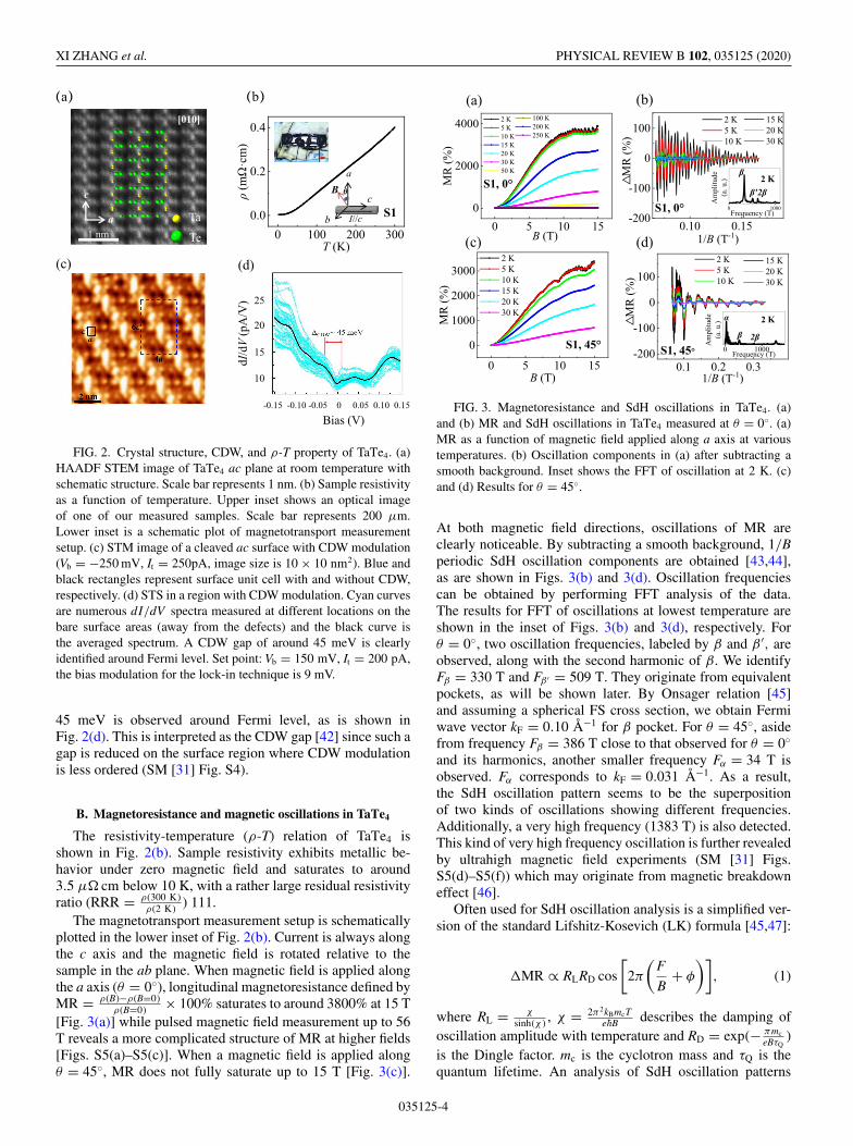
FIG. 2. Crystal structure, CDW, and ρ-T property of TaTe4. (a)HAADF STEM image of TaTe4 ac plane at room temperature withschematic structure. Scale bar represents 1 nm. (b) Sample resistivityas a function of temperature. Upper inset shows an optical imageof one of our measured samples. Scale bar represents 200 μm.Lower inset is a schematic plot of magnetotransport measurementsetup. (c) STM image of a cleaved ac surface with CDW modulation(Vb = −250 mV, It = 250pA, image size is 10 × 10 nm2). Blue andblack rectangles represent surface unit cell with and without CDW,respectively. (d) STS in a region with CDW modulation. Cyan curvesare numerous dI/dV spectra measured at different locations on thebare surface areas (away from the defects) and the black curve isthe averaged spectrum. A CDW gap of around 45 meV is clearlyidentified around Fermi level. Set point: Vb = 150 mV, It = 200 pA,the bias modulation for the lock-in technique is 9 mV.
45 meV is observed around Fermi level, as is shown inFig. 2(d). This is interpreted as the CDW gap [42] since such agap is reduced on the surface region where CDW modulationis less ordered (SM [31] Fig. S4).
B. Magnetoresistance and magnetic oscillations in TaTe4
The resistivity-temperature (ρ-T) relation of TaTe4 isshown in Fig. 2(b). Sample resistivity exhibits metallic be-havior under zero magnetic field and saturates to around3.5 μ� cm below 10 K, with a rather large residual resistivityratio (RRR = ρ(300 K)
ρ(2 K) ) 111.The magnetotransport measurement setup is schematically
plotted in the lower inset of Fig. 2(b). Current is always alongthe c axis and the magnetic field is rotated relative to thesample in the ab plane. When magnetic field is applied alongthe a axis (θ = 0◦), longitudinal magnetoresistance defined byMR = ρ(B)−ρ(B=0)
ρ(B=0) × 100% saturates to around 3800% at 15 T[Fig. 3(a)] while pulsed magnetic field measurement up to 56T reveals a more complicated structure of MR at higher fields[Figs. S5(a)–S5(c)]. When a magnetic field is applied alongθ = 45◦, MR does not fully saturate up to 15 T [Fig. 3(c)].
0 5 10 150
2000
4000 100 K 200 K 250 K
)%(
RM
B (T)
2 K 5 K 10 K 15 K 20 K 30 K 50 K
S1, 0°
0 5 10 15
0
1000
2000
3000
)%(
RM
B (T)
2 K 5 K 10 K 15 K 20 K 30 K
S1, 45°
0.1 0.2 0.3-200
-100
0
100 15 K 20 K 30 K)
%( R
M
1/B (T-1)
2 K 5 K 10 K
S1, 45°
0.10 0.15-200
-100
0
100 15 K 20 K 30 K)
%( R
M
1/B (T-1)
2 K 5 K 10 K
S1, 0°
(a) (b)
(c) (d)
(a. u
.)
Frequency (T)
0 1000
edutilpm
A(a
. u.)
Frequency (T)
2 K
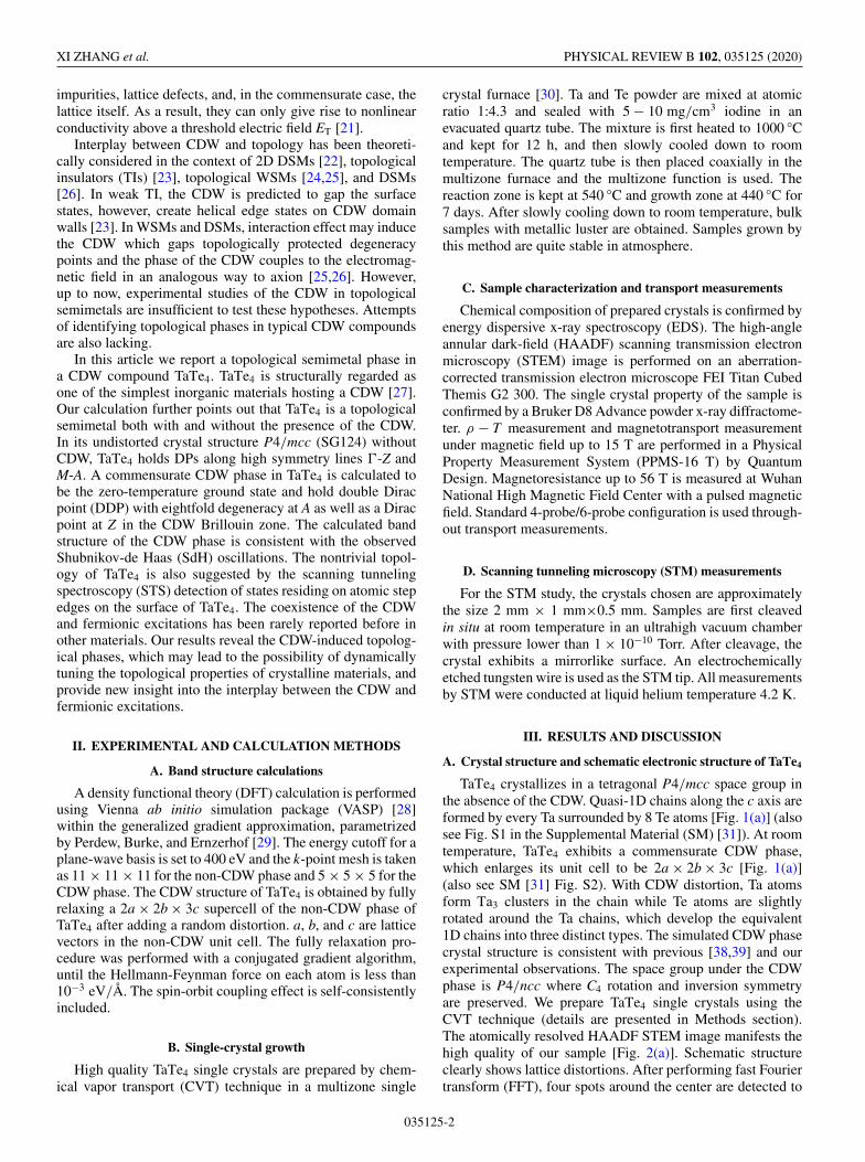
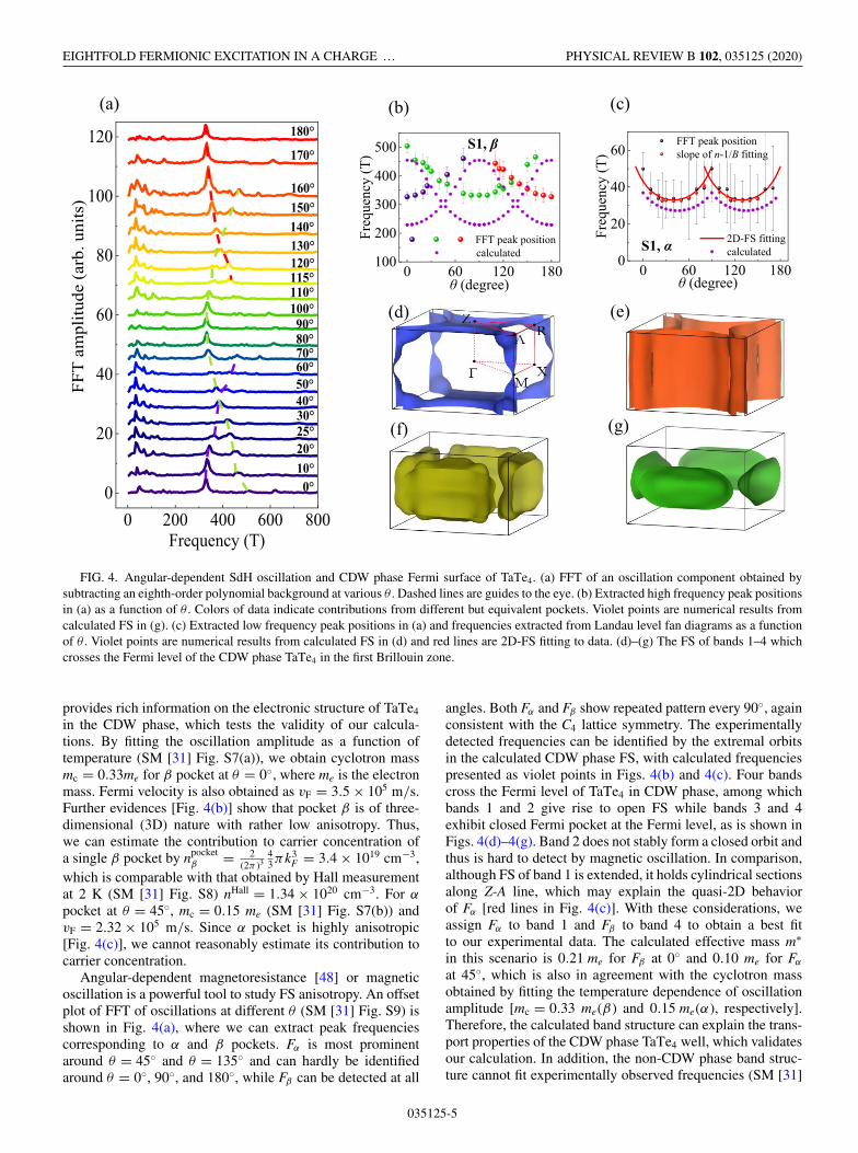
FIG. 3. Magnetoresistance and SdH oscillations in TaTe4. (a)and (b) MR and SdH oscillations in TaTe4 measured at θ = 0◦. (a)MR as a function of magnetic field applied along a axis at varioustemperatures. (b) Oscillation components in (a) after subtracting asmooth background. Inset shows the FFT of oscillation at 2 K. (c)and (d) Results for θ = 45◦.
At both magnetic field directions, oscillations of MR areclearly noticeable. By subtracting a smooth background, 1/Bperiodic SdH oscillation components are obtained [43,44],as are shown in Figs. 3(b) and 3(d). Oscillation frequenciescan be obtained by performing FFT analysis of the data.The results for FFT of oscillations at lowest temperature areshown in the inset of Figs. 3(b) and 3(d), respectively. Forθ = 0◦, two oscillation frequencies, labeled by β and β ′, areobserved, along with the second harmonic of β. We identifyFβ = 330 T and Fβ ′ = 509 T. They originate from equivalentpockets, as will be shown later. By Onsager relation [45]and assuming a spherical FS cross section, we obtain Fermiwave vector kF = 0.10 Å−1 for β pocket. For θ = 45◦, asidefrom frequency Fβ = 386 T close to that observed for θ = 0◦and its harmonics, another smaller frequency Fα = 34 T isobserved. Fα corresponds to kF = 0.031 Å−1. As a result,the SdH oscillation pattern seems to be the superpositionof two kinds of oscillations showing different frequencies.Additionally, a very high frequency (1383 T) is also detected.This kind of very high frequency oscillation is further revealedby ultrahigh magnetic field experiments (SM [31] Figs.S5(d)–S5(f)) which may originate from magnetic breakdowneffect [46].
Often used for SdH oscillation analysis is a simplified ver-sion of the standard Lifshitz-Kosevich (LK) formula [45,47]:
�MR ∝ RLRD cos
[2π
(F
B+ φ
)], (1)
where RL = χ
sinh(χ ) , χ = 2π2kBmcTeh̄B describes the damping of
oscillation amplitude with temperature and RD = exp(− πmceBτQ
)is the Dingle factor. mc is the cyclotron mass and τQ is thequantum lifetime. An analysis of SdH oscillation patterns
035125-4
EIGHTFOLD FERMIONIC EXCITATION IN A CHARGE … PHYSICAL REVIEW B 102, 035125 (2020)
0 200 400 600 8000
20
40
60
80
100
120
(a
rb. u
nits
) edutilp
ma TFF
Frequency (T)
0°10°20°25°
60°50°40°30°
70°80°90°
100°
130°120°115°110°
140°150°160°
170°
180°
(a) (b) (c)
(d) (e)
(f)
0 60 120 1800
20
40
60 FFT peak position slope of n-1/B fitting
2D-FS fitting calculated
)T( ycneuqerF
(degree)
S1,
0 60 120 180100
200
300
400
500
FFT peak position calculated
)T( ycneuqerF
(degree)
S1,
(g)
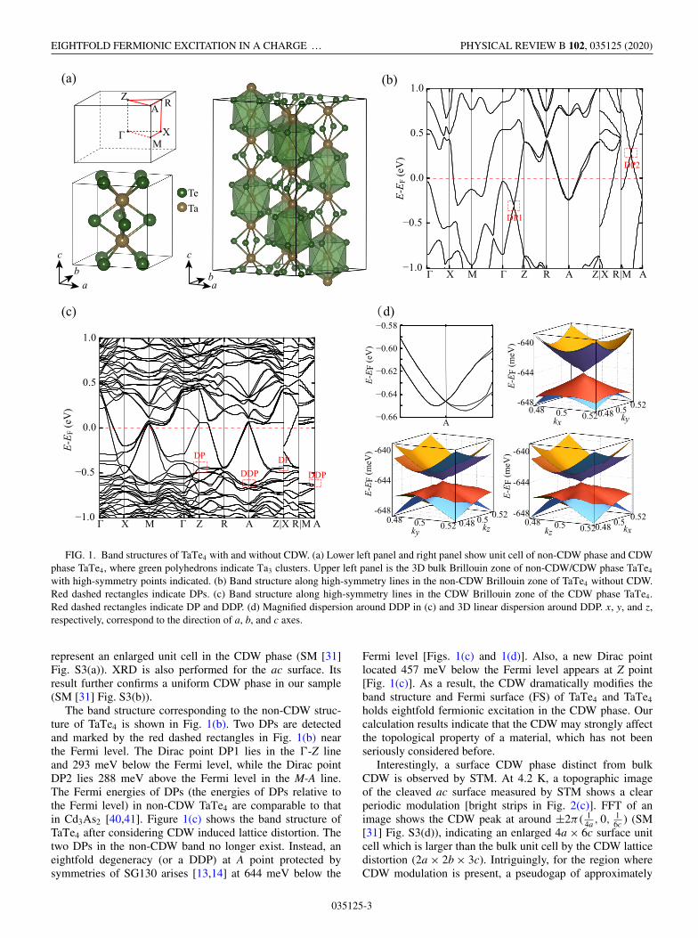
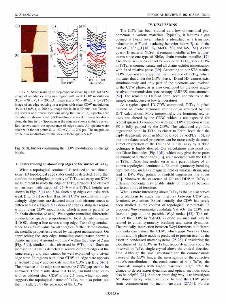
FIG. 4. Angular-dependent SdH oscillation and CDW phase Fermi surface of TaTe4. (a) FFT of an oscillation component obtained bysubtracting an eighth-order polynomial background at various θ . Dashed lines are guides to the eye. (b) Extracted high frequency peak positionsin (a) as a function of θ . Colors of data indicate contributions from different but equivalent pockets. Violet points are numerical results fromcalculated FS in (g). (c) Extracted low frequency peak positions in (a) and frequencies extracted from Landau level fan diagrams as a functionof θ . Violet points are numerical results from calculated FS in (d) and red lines are 2D-FS fitting to data. (d)–(g) The FS of bands 1–4 whichcrosses the Fermi level of the CDW phase TaTe4 in the first Brillouin zone.
provides rich information on the electronic structure of TaTe4
in the CDW phase, which tests the validity of our calcula-tions. By fitting the oscillation amplitude as a function oftemperature (SM [31] Fig. S7(a)), we obtain cyclotron massmc = 0.33me for β pocket at θ = 0◦, where me is the electronmass. Fermi velocity is also obtained as vF = 3.5 × 10⁵ m/s.Further evidences [Fig. 4(b)] show that pocket β is of three-dimensional (3D) nature with rather low anisotropy. Thus,we can estimate the contribution to carrier concentration ofa single β pocket by npocket
β = 2(2π )3
43πk3
F = 3.4 × 1019 cm−3,which is comparable with that obtained by Hall measurementat 2 K (SM [31] Fig. S8) nHall = 1.34 × 1020 cm−3. For α
pocket at θ = 45◦, mc = 0.15 me (SM [31] Fig. S7(b)) andvF = 2.32 × 10⁵ m/s. Since α pocket is highly anisotropic[Fig. 4(c)], we cannot reasonably estimate its contribution tocarrier concentration.
Angular-dependent magnetoresistance [48] or magneticoscillation is a powerful tool to study FS anisotropy. An offsetplot of FFT of oscillations at different θ (SM [31] Fig. S9) isshown in Fig. 4(a), where we can extract peak frequenciescorresponding to α and β pockets. Fα is most prominentaround θ = 45◦ and θ = 135◦ and can hardly be identifiedaround θ = 0◦, 90◦, and 180◦, while Fβ can be detected at all
angles. Both Fα and Fβ show repeated pattern every 90◦, againconsistent with the C4 lattice symmetry. The experimentallydetected frequencies can be identified by the extremal orbitsin the calculated CDW phase FS, with calculated frequenciespresented as violet points in Figs. 4(b) and 4(c). Four bandscross the Fermi level of TaTe4 in CDW phase, among whichbands 1 and 2 give rise to open FS while bands 3 and 4exhibit closed Fermi pocket at the Fermi level, as is shown inFigs. 4(d)–4(g). Band 2 does not stably form a closed orbit andthus is hard to detect by magnetic oscillation. In comparison,although FS of band 1 is extended, it holds cylindrical sectionsalong Z-A line, which may explain the quasi-2D behaviorof Fα [red lines in Fig. 4(c)]. With these considerations, weassign Fα to band 1 and Fβ to band 4 to obtain a best fitto our experimental data. The calculated effective mass m∗in this scenario is 0.21 me for Fβ at 0◦ and 0.10 me for Fα
at 45◦, which is also in agreement with the cyclotron massobtained by fitting the temperature dependence of oscillationamplitude [mc = 0.33 me(β ) and 0.15 me(α), respectively].Therefore, the calculated band structure can explain the trans-port properties of the CDW phase TaTe4 well, which validatesour calculation. In addition, the non-CDW phase band struc-ture cannot fit experimentally observed frequencies (SM [31]
035125-5
XI ZHANG et al. PHYSICAL REVIEW B 102, 035125 (2020)
(b)
(a)
8 nm
8 nm -100 0 1000
20
40
60
80
)V/
Ap(Vd/Id
Bias(mV)-100 0 100
0
20
40
60
80
)V/
Ap(Vd/Id
Bias(mV)
(c) (d)
dI/dV
(pA
/V)
Bias (mV) Bias (mV)dI
/dV
(pA
/V)
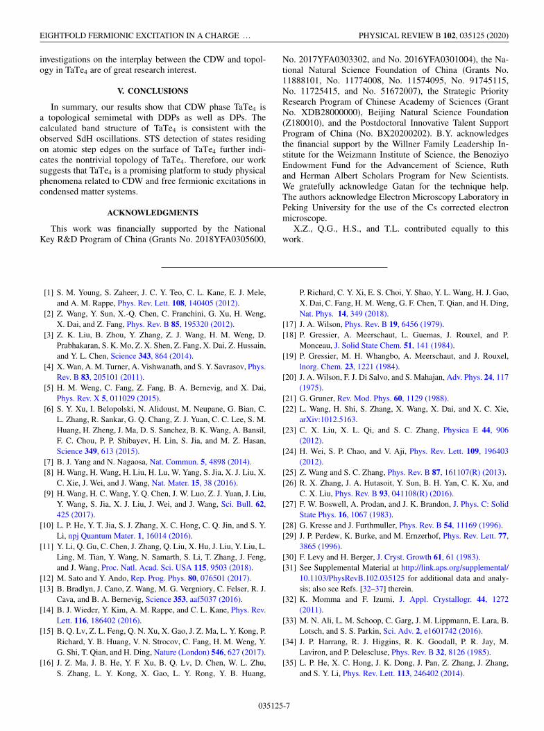
FIG. 5. States residing on step edges observed by STM. (a) STMimage of an edge existing in a region with weak CDW modulation(Vb = −70 mV, It = 200 pA, image size is 40 × 40 nm2). (b) STMimage of an edge existing in a region with clear CDW modulation(Vb = 12 mV, It = 200 pA, image size is 40 × 40 nm2). (c) Tunnel-ing spectra at different locations along the line in (a). Spectra nearthe edge are shown in red. (d) Tunneling spectra at different locationsalong the line in (b). Spectra near the edge are shown in thick curves.Red arrows mark the appearance of edge states. All spectra weretaken with the set point: Vb = 150 mV, It = 200 pA. The magnitudeof the bias modulation for the lock-in technique is 9 mV.
Fig. S10), further confirming the CDW modulation on energybands.
C. States residing on atomic step edges on the surface of TaTe4
When a topological semimetal is reduced to two dimen-sions, 1D topological edge states could be detected. To furtherconfirm the topological property of TaTe4, we carry out STMmeasurement to study the edge of TaTe4 terraces. The cleavedac surfaces with steps of 2b (b = a in TaTe4) height areshown in Figs. 5(a) and 5(b). Such step edges can exist withweak [Fig. 5(a)] or clear [Fig. 5(b)] CDW modulation. Inter-estingly, edge states are detected under both circumstances atdifferent biases. Figure 5(a) shows an edge existing in a regionwithout clear CDW modulation, which is mostly parallel toTa chain direction (c axis). We acquire tunneling differentialconductance spectra, proportional to local density of states(LDOS), along a line across a step edge. Tunneling conduc-tance has a finite value for all energies, further demonstratingthe metallic properties revealed by transport measurement. Onapproaching the step edge, tunneling conductance shows adrastic increase at around −75 meV within the range of 2 nm[Fig. 5(c)], similar to that observed in WTe2 [49]. Such anincrease in LDOS is detected at several different edges at thesame energy and thus cannot be well explained by a trivialedge state. In regions with clear CDW, an edge state appearsat around 12 meV and coexists with the CDW gap [Fig. 5(d)].The presence of the edge state makes the CDW gap seem to benarrower. These results show that TaTe4 can hold edge stateswith or without clear CDW in the 2D limit, which not onlysuggests the topological nature of TaTe4 but also points outthat it is altered by the presence of the CDW.
IV. DISCUSSIONS
The CDW has been studied as a low dimensional phe-nomenon in various materials. Typically, it features a gapopened at Fermi level, which is identified as a transitionbehavior in ρ-T and insulating behavior below Tp, as in thecase of (TaSe4)2I [18], K0.3MoO3 [50], and TaS3 [51]. As forquasi-1D material NbSe3, it remains metallic at low temper-atures since one type of NbSe3 chain remains metallic [17].The above scenarios cannot be applied to TaTe4, since CDWin TaTe4 is commensurate and all chains exhibit trimerizationwith fixed relative phase [39]. According to our STS results,CDW does not fully gap the Fermi surface of TaTe4, whichindicates that under the CDW phase, 1D and 3D features existsimultaneously and only part of the electrons are involvedin the CDW phase, as is also concluded by previous angle-resolved photoemission spectroscopy (ARPES) measurement[52]. The remaining DOS at Fermi level contributes to thesample conductance at low temperatures.
As a typical quasi-1D CDW compound, TaTe4 is giftedto hold an exotic fermionic excitation as revealed by ourDFT calculations. More interestingly, the fermionic excita-tions are altered by the CDW, which is not expected fortypical quasi-1D compounds with the CDW transition whoseFS is fully gapped by the CDW. The calculated eightfolddegenerate point in TaTe4 is closer to Fermi level than thetriply degenerate point in MoP observed by ARPES [15], sothat the related novel properties can be more easily detected.Direct observation of the DDP and DP in TaTe4 by ARPEStechnique is highly desired. Our calculations also point outthat Dirac line nodes [Fig. 1(d)], which may give rise to pairsof drumhead surface states [13], are associated with the DDPin TaTe4. Dirac line nodes serve as a parent phase of allknown topological semimetals. External symmetry-breakingperturbations, such as a magnetic field or uniaxial strain, maylead to DPs, Weyl points, or twofold degenerate line nodes[13]. Moreover, the existence of DP and DDP in TaTe4 atdifferent momenta may enable study of interplay betweendifferent kinds of fermions.
What is more interesting about TaTe4 is that it also servesas a platform to study the interplay between CDW andfermionic excitations. Experimentally, the CDW has rarelybeen studied in the context of topological semimetals. Inproposed Weyl semimetal candidate Y2Ir2O7, the CDW wasfound to gap out the possible Weyl nodes [53]. The ori-gin of the CDW in Y2Ir2O7 is quite unusual and may berelated to chiral symmetry breaking and axion dynamics.Theoretically, interaction between Weyl fermions at differentmomenta can induce the CDW, which gaps Weyl or Diracpoints and the phase mode is predicted to present itself as theaxion in condensed matter systems [25,26]. Considering therobustness of the CDW in TaTe4, axion dynamics could beobserved in TaTe4 single crystal above the critical electricalfield. Although the small resistance and the commensuratenature of the CDW hinder the investigation of the collectivemode’s contribution to the conductance of bulk TaTe4, thenanoscale samples with higher resistance might offer thechance to detect axion dynamics and optical methods couldalso be helpful [21]. Another promising way is to investigateNb doped TaTe4, which is found to tune the CDW phasefrom commensurate to incommensurate [27,54]. Further
035125-6
EIGHTFOLD FERMIONIC EXCITATION IN A CHARGE … PHYSICAL REVIEW B 102, 035125 (2020)
investigations on the interplay between the CDW and topol-ogy in TaTe4 are of great research interest.
V. CONCLUSIONS
In summary, our results show that CDW phase TaTe4 isa topological semimetal with DDPs as well as DPs. Thecalculated band structure of TaTe4 is consistent with theobserved SdH oscillations. STS detection of states residingon atomic step edges on the surface of TaTe4 further indi-cates the nontrivial topology of TaTe4. Therefore, our worksuggests that TaTe4 is a promising platform to study physicalphenomena related to CDW and free fermionic excitations incondensed matter systems.
ACKNOWLEDGMENTS
This work was financially supported by the NationalKey R&D Program of China (Grants No. 2018YFA0305600,
No. 2017YFA0303302, and No. 2016YFA0301004), the Na-tional Natural Science Foundation of China (Grants No.11888101, No. 11774008, No. 11574095, No. 91745115,No. 11725415, and No. 51672007), the Strategic PriorityResearch Program of Chinese Academy of Sciences (GrantNo. XDB28000000), Beijing Natural Science Foundation(Z180010), and the Postdoctoral Innovative Talent SupportProgram of China (No. BX20200202). B.Y. acknowledgesthe financial support by the Willner Family Leadership In-stitute for the Weizmann Institute of Science, the BenoziyoEndowment Fund for the Advancement of Science, Ruthand Herman Albert Scholars Program for New Scientists.We gratefully acknowledge Gatan for the technique help.The authors acknowledge Electron Microscopy Laboratory inPeking University for the use of the Cs corrected electronmicroscope.
X.Z., Q.G., H.S., and T.L. contributed equally to thiswork.
[1] S. M. Young, S. Zaheer, J. C. Y. Teo, C. L. Kane, E. J. Mele,and A. M. Rappe, Phys. Rev. Lett. 108, 140405 (2012).
[2] Z. Wang, Y. Sun, X.-Q. Chen, C. Franchini, G. Xu, H. Weng,X. Dai, and Z. Fang, Phys. Rev. B 85, 195320 (2012).
[3] Z. K. Liu, B. Zhou, Y. Zhang, Z. J. Wang, H. M. Weng, D.Prabhakaran, S. K. Mo, Z. X. Shen, Z. Fang, X. Dai, Z. Hussain,and Y. L. Chen, Science 343, 864 (2014).
[4] X. Wan, A. M. Turner, A. Vishwanath, and S. Y. Savrasov, Phys.Rev. B 83, 205101 (2011).
[5] H. M. Weng, C. Fang, Z. Fang, B. A. Bernevig, and X. Dai,Phys. Rev. X 5, 011029 (2015).
[6] S. Y. Xu, I. Belopolski, N. Alidoust, M. Neupane, G. Bian, C.L. Zhang, R. Sankar, G. Q. Chang, Z. J. Yuan, C. C. Lee, S. M.Huang, H. Zheng, J. Ma, D. S. Sanchez, B. K. Wang, A. Bansil,F. C. Chou, P. P. Shibayev, H. Lin, S. Jia, and M. Z. Hasan,Science 349, 613 (2015).
[7] B. J. Yang and N. Nagaosa, Nat. Commun. 5, 4898 (2014).[8] H. Wang, H. Wang, H. Liu, H. Lu, W. Yang, S. Jia, X. J. Liu, X.
C. Xie, J. Wei, and J. Wang, Nat. Mater. 15, 38 (2016).[9] H. Wang, H. C. Wang, Y. Q. Chen, J. W. Luo, Z. J. Yuan, J. Liu,
Y. Wang, S. Jia, X. J. Liu, J. Wei, and J. Wang, Sci. Bull. 62,425 (2017).
[10] L. P. He, Y. T. Jia, S. J. Zhang, X. C. Hong, C. Q. Jin, and S. Y.Li, npj Quantum Mater. 1, 16014 (2016).
[11] Y. Li, Q. Gu, C. Chen, J. Zhang, Q. Liu, X. Hu, J. Liu, Y. Liu, L.Ling, M. Tian, Y. Wang, N. Samarth, S. Li, T. Zhang, J. Feng,and J. Wang, Proc. Natl. Acad. Sci. USA 115, 9503 (2018).
[12] M. Sato and Y. Ando, Rep. Prog. Phys. 80, 076501 (2017).[13] B. Bradlyn, J. Cano, Z. Wang, M. G. Vergniory, C. Felser, R. J.
Cava, and B. A. Bernevig, Science 353, aaf5037 (2016).[14] B. J. Wieder, Y. Kim, A. M. Rappe, and C. L. Kane, Phys. Rev.
Lett. 116, 186402 (2016).[15] B. Q. Lv, Z. L. Feng, Q. N. Xu, X. Gao, J. Z. Ma, L. Y. Kong, P.
Richard, Y. B. Huang, V. N. Strocov, C. Fang, H. M. Weng, Y.G. Shi, T. Qian, and H. Ding, Nature (London) 546, 627 (2017).
[16] J. Z. Ma, J. B. He, Y. F. Xu, B. Q. Lv, D. Chen, W. L. Zhu,S. Zhang, L. Y. Kong, X. Gao, L. Y. Rong, Y. B. Huang,
P. Richard, C. Y. Xi, E. S. Choi, Y. Shao, Y. L. Wang, H. J. Gao,X. Dai, C. Fang, H. M. Weng, G. F. Chen, T. Qian, and H. Ding,Nat. Phys. 14, 349 (2018).
[17] J. A. Wilson, Phys. Rev. B 19, 6456 (1979).[18] P. Gressier, A. Meerschaut, L. Guemas, J. Rouxel, and P.
Monceau, J. Solid State Chem. 51, 141 (1984).[19] P. Gressier, M. H. Whangbo, A. Meerschaut, and J. Rouxel,
lnorg. Chem. 23, 1221 (1984).[20] J. A. Wilson, F. J. Di Salvo, and S. Mahajan, Adv. Phys. 24, 117
(1975).[21] G. Gruner, Rev. Mod. Phys. 60, 1129 (1988).[22] L. Wang, H. Shi, S. Zhang, X. Wang, X. Dai, and X. C. Xie,
arXiv:1012.5163.[23] C. X. Liu, X. L. Qi, and S. C. Zhang, Physica E 44, 906
(2012).[24] H. Wei, S. P. Chao, and V. Aji, Phys. Rev. Lett. 109, 196403
(2012).[25] Z. Wang and S. C. Zhang, Phys. Rev. B 87, 161107(R) (2013).[26] R. X. Zhang, J. A. Hutasoit, Y. Sun, B. H. Yan, C. K. Xu, and
C. X. Liu, Phys. Rev. B 93, 041108(R) (2016).[27] F. W. Boswell, A. Prodan, and J. K. Brandon, J. Phys. C: Solid
State Phys. 16, 1067 (1983).[28] G. Kresse and J. Furthmuller, Phys. Rev. B 54, 11169 (1996).[29] J. P. Perdew, K. Burke, and M. Ernzerhof, Phys. Rev. Lett. 77,
3865 (1996).[30] F. Levy and H. Berger, J. Cryst. Growth 61, 61 (1983).[31] See Supplemental Material at http://link.aps.org/supplemental/
10.1103/PhysRevB.102.035125 for additional data and analy-sis; also see Refs. [32–37] therein.
[32] K. Momma and F. Izumi, J. Appl. Crystallogr. 44, 1272(2011).
[33] M. N. Ali, L. M. Schoop, C. Garg, J. M. Lippmann, E. Lara, B.Lotsch, and S. S. Parkin, Sci. Adv. 2, e1601742 (2016).
[34] J. P. Harrang, R. J. Higgins, R. K. Goodall, P. R. Jay, M.Laviron, and P. Delescluse, Phys. Rev. B 32, 8126 (1985).
[35] L. P. He, X. C. Hong, J. K. Dong, J. Pan, Z. Zhang, J. Zhang,and S. Y. Li, Phys. Rev. Lett. 113, 246402 (2014).
035125-7
XI ZHANG et al. PHYSICAL REVIEW B 102, 035125 (2020)
[36] Y. F. Zhao, H. W. Liu, C. L. Zhang, H. C. Wang, J. F. Wang, Z.Q. Lin, Y. Xing, H. Lu, J. Liu, Y. Wang, S. M. Brombosz, Z. L.Xiao, S. Jia, X. C. Xie, and J. Wang, Phys. Rev. X 5, 031037(2015).
[37] C. M. Wang, H. Z. Lu, and S. Q. Shen, Phys. Rev. Lett. 117,077201 (2016).
[38] K. D. Bronsema, S. Vansmaalen, J. L. Deboer, G. A. Wiegers, F.Jellinek, and J. Mahy, Acta Crystallogr. Sect. B 43, 305 (1987).
[39] J. M. Corbett, L. G. Hiltz, F. W. Boswell, J. C. Bennett, and A.Prodan, Ultramicroscopy 26, 43 (1988).
[40] S. Jeon, B. B. Zhou, A. Gyenis, B. E. Feldman, I. Kimchi, A.C. Potter, Q. D. Gibson, R. J. Cava, A. Vishwanath, and A.Yazdani, Nat. Mater. 13, 851 (2014).
[41] T. Liang, Q. Gibson, M. N. Ali, M. Liu, R. J. Cava, and N. P.Ong, Nat. Mater. 14, 280 (2015).
[42] P. Chen, W. W. Pai, Y. H. Chan, A. Takayama, C. Z. Xu, A.Karn, S. Hasegawa, M. Y. Chou, S. K. Mo, A. V. Fedorov, andT. C. Chiang, Nat. Commun. 8, 516 (2017).
[43] Y. X. Gao, L. M. Xu, Y. Qiu, Z. M. Tian, S. L. Yuan, and J. F.Wang, J. Appl. Phys. 122, 135101 (2017).
[44] X. Luo, F. C. Chen, Q. L. Pei, J. J. Gao, J. Yan, W. J. Lu, P.Tong, Y. Y. Han, W. H. Song, and Y. P. Sun, Appl. Phys. Lett.110, 092401 (2017).
[45] D. Shoenberg, Magnetic Oscillations in Metals (CambridgeUniversity Press, Cambridge, 1984).
[46] S. Pezzini, M. R. van Delft, L. M. Schoop, B. V. Lotsch, A.Carrington, M. I. Katsnelson, N. E. Hussey, and S. Wiedmann,Nat. Phys. 14, 178 (2018).
[47] D. X. Qu, Y. S. Hor, J. Xiong, R. J. Cava, and N. P. Ong, Science329, 821 (2010).
[48] X. Zhang, T. Luo, X. Hu, J. Guo, G. Lin, Y. Li, Y. Liu, X. Li, J.Ge, Y. Xing, Z. Zhu, P. Gao, L. Sun, and J. Wang, Chin. Phys.Lett. 36, 057402 (2019).
[49] L. Peng, Y. Yuan, G. Li, X. Yang, J. J. Xian, C. J. Yi, Y. G. Shi,and Y. S. Fu, Nat. Commun. 8, 659 (2017).
[50] X. M. Wang, L. Lu, H. M. Duan, B. J. Jin, and D. L. Zhang,Solid State Commun. 69, 829 (1989).
[51] T. Sambongi, K. Tsutsumi, Y. Shiozaki, M. Yamamoto, K.Yamaya, and Y. Abe, Solid State Commun. 22, 729 (1977).
[52] F. Zwick, H. Berger, M. Grioni, G. Margaritondo, L. Forro, J.LaVeigne, D. B. Tanner, and M. Onellion, Phys. Rev. B 59, 7762(1999).
[53] A. Juyal, A. Agarwal, and S. Mukhopadhyay, Phys. Rev. Lett.120, 096801 (2018).
[54] A. Prodan, V. Marinkovic, F. W. Boswell, J. C. Bennett, and M.Remskar, J. Alloy. Compd. 219, 69 (1995).
035125-8