Embed Size (px)
Citation preview
Lab 7 - 1
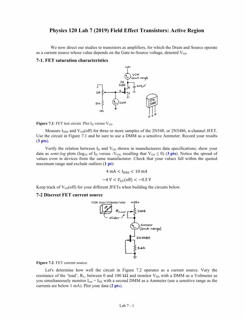
Physics 120 Lab 7 (2019) Field Effect Transistors: Active Region
We now direct our studies to transistors as amplifiers, for which the Drain and Source operate as a current source whose value depends on the Gate-to-Source voltage, denoted VGS.
7-1. FET saturation characteristics
Figure 7.1: FET test circuit. Plot ID versus VGS.
Measure IDSS and VGS(off) for three or more samples of the 2N548, or 2N5486, n-channel JFET. Use the circuit in Figure 7.1 and be sure to use a DMM as a sensitive Ammeter. Record your results (3 pts).
Verify the relation between ID and VGS shown in manufacturers data specifications; show your data as semi-log plots (log10 of ID versus -VGS, recalling that VGS ≤ 0) (3 pts). Notice the spread of values even in devices from the same manufacturer. Check that your values fall within the quoted maximum range and exclude outliers (1 pt):
4 mA < I!"" < 10 mA
−4 V < 𝑉!"(off) < −0.5 V
Keep track of VGS(off) for your different JFETs when building the circuits below.
7-2 Discreet FET current source
Figure 7.2: FET current source.
Let's determine how well the circuit in Figure 7.2 operates as a current source. Vary the resistance of the ‘load’, RL, between 0 and 100 kΩ and monitor VDS with a DMM as a Voltmeter as you simultaneously monitor Iout = IDS with a second DMM as a Ammeter (use a sensitive range as the currents are below 1 mA). Plot your data (2 pts).
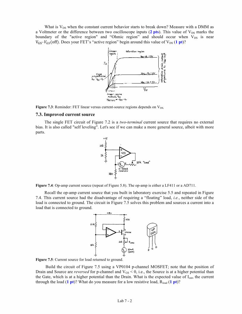
Lab 7 - 2
What is VDS when the constant current behavior starts to break down? Measure with a DMM as a Voltmeter or the difference between two oscilloscope inputs (2 pts). This value of VDS marks the boundary of the "active region" and “Ohmic region” and should occur when VDS is near V!"!𝑉!"(off). Does your FET’s “active region” begin around this value of VDS (1 pt)?
Figure 7.3: Reminder: FET linear versus current-source regions depends on VDS.
7.3. Improved current source The single FET circuit of Figure 7.2 is a two-terminal current source that requires no external
bias. It is also called "self leveling". Let's see if we can make a more general source, albeit with more parts.
Figure 7.4: Op-amp current source (repeat of Figure 5.8). The op-amp is either a LF411 or a AD711.
Recall the op-amp current source that you built in laboratory exercise 5.5 and repeated in Figure 7.4. This current source had the disadvantage of requiring a “floating” load, i.e., neither side of the load is connected to ground. The circuit in Figure 7.5 solves this problem and sources a current into a load that is connected to ground.
Figure 7.5: Current source for load returned to ground.
Build the circuit of Figure 7.5 using a VP0104 p-channel MOSFET; note that the position of Drain and Source are reversed for p-channel and VGS < 0, i.e., the Source is at a higher potential than the Gate, which is at a higher potential than the Drain. What is the expected value of Iout, the current through the load (1 pt)? What do you measure for a low resistive load, Rload (1 pt)?
Lab 7 - 3
Measure the variation in Iout as you vary Rload. To understand why the current source eventually fails, it may help to use a Voltmeter (or the difference between two oscilloscope channels) to watch the voltage across the FET, i.e., VDS. Present your result (2 pts). Briefly discuss if the FET’s Ohmic region, i.e., the region with VDS below VGS - VGS(off), restricts the range of circuit performance as it did for the discrete FET current source (section 7.2) (1 pt).
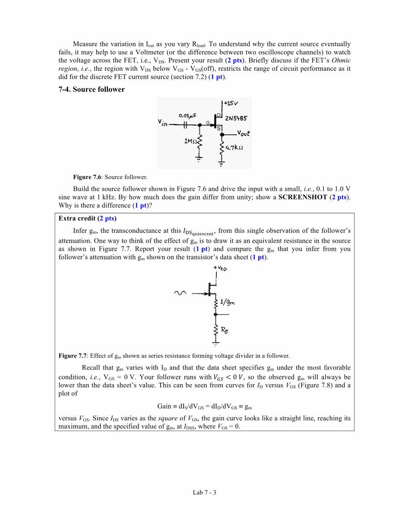
7-4. Source follower
Figure 7.6: Source follower.
Build the source follower shown in Figure 7.6 and drive the input with a small, i.e., 0.1 to 1.0 V sine wave at 1 kHz. By how much does the gain differ from unity; show a SCREENSHOT (2 pts). Why is there a difference (1 pt)?
Extra credit (2 pts)
Infer gm, the transconductance at this 𝐼!"!"#$%&$'(, from this single observation of the follower’s attenuation. One way to think of the effect of gm is to draw it as an equivalent resistance in the source as shown in Figure 7.7. Report your result (1 pt) and compare the gm that you infer from you follower’s attenuation with gm shown on the transistor’s data sheet (1 pt).
Figure 7.7: Effect of gm shown as series resistance forming voltage divider in a follower.
Recall that gm varies with ID and that the data sheet specifies gm under the most favorable condition, i.e., VGS = 0 V. Your follower runs with 𝑉!" < 0 𝑉, so the observed gm will always be lower than the data sheet’s value. This can be seen from curves for ID versus VGS (Figure 7.8) and a plot of
Gain ≡ dIS/dVGS = dID/dVGS ≡ gm
versus VGS. Since IDS varies as the square of VGS, the gain curve looks like a straight line, reaching its maximum, and the specified value of gm, at IDSS, where VGS = 0.

Lab 7 - 4
Figure 7.8: ID versus VGS, andgain versus VGS. Gain varies linearly with VGS – VGS(off).
From your observation of the selected, quiescent value of VDS, denoted VDS-quiescent; you know VGS-
quiescent; recall that VG rests at ground through the 1 MΩ pull-down resistor. Having measured VGS(off) at the start of today’s laboratory, you can see where you must be on the FET’s curve. Make a sketch (2 pts).
7.5. Source follower with current source load Modify the circuit of Figure 7.6 to include a current source load, as shown in Figure 7.9.
Confirm that this follower performs much better than the simpler circuit.
Figure 7.9: Low-Offset source follower with current source load.
Measure the gain with a 1 V, 1 kHz signal and document with a SCREENSHOT (1 pt). Is the gain closer to 1.0 than with simple follower of Figure 7.6 (1 pt)? Is the offset closer to zero volts than with simple follower of Figure 7.6 (1 pt)?
Attempt to measure the input impedance. Document your work and report at least a lower bound (2 pts). Hint: If you conclude that Rin is around 10 MΩ ohms, you have likely fallen into a trap!
Measure the DC offset and Is there a measureable DC offset? document with a SCREENSHOT (1 pt). What does or could accounts for a non-zero offset (1 pt)? Mismatch of FETs? Mismatch of resistors? Anything else? What easy circuit changes would let you find out, if you are in doubt (1 pt)?
30 points total
2 point bonus

![[Chapter III] Basic Knowledge of Discrete Semiconductor ......transistors (IGBTs) Power transistors (2SAxx,2SBxx,2SCxx,2SDxx, TTAxx,TTBxx,TTCxx,TTDxx) Types of Transistors Transistors](https://img.pdfslide.net/doc/110x75/5e766014341a1a707d5f4c34/chapter-iii-basic-knowledge-of-discrete-semiconductor-transistors-igbts.jpg)