Embed Size (px)
Citation preview

This article was downloaded by: [Boston College]On: 04 August 2011, At: 05:44Publisher: Taylor & FrancisInforma Ltd Registered in England and Wales Registered Number: 1072954 Registeredoffice: Mortimer House, 37-41 Mortimer Street, London W1T 3JH, UK
Advances in PhysicsPublication details, including instructions for authors andsubscription information:http://www.tandfonline.com/loi/tadp20
Physics and applications of alignedcarbon nanotubesYucheng Lan a , Yang Wang b & Z. F. Ren aa Department of Physics, Boston College, Chestnut Hill, MA,02467, USAb School of Physics and Telecommunication Engineering, SouthChina Normal University, Higher Education Mega Center,Guangzhou, 510006, China
Available online: 04 Aug 2011
To cite this article: Yucheng Lan, Yang Wang & Z. F. Ren (2011): Physics and applications of alignedcarbon nanotubes, Advances in Physics, 60:4, 553-678
To link to this article: http://dx.doi.org/10.1080/00018732.2011.599963
PLEASE SCROLL DOWN FOR ARTICLE
Full terms and conditions of use: http://www.tandfonline.com/page/terms-and-conditions
This article may be used for research, teaching and private study purposes. Anysubstantial or systematic reproduction, re-distribution, re-selling, loan, sub-licensing,systematic supply or distribution in any form to anyone is expressly forbidden.
The publisher does not give any warranty express or implied or make any representationthat the contents will be complete or accurate or up to date. The accuracy of anyinstructions, formulae and drug doses should be independently verified with primarysources. The publisher shall not be liable for any loss, actions, claims, proceedings,demand or costs or damages whatsoever or howsoever caused arising directly orindirectly in connection with or arising out of the use of this material.

Advances in PhysicsVol. 60, No. 4, July–August 2011, 553–678
REVIEW ARTICLE
Physics and applications of aligned carbon nanotubes
Yucheng Lana, Yang Wangb and Z.F. Rena*
aDepartment of Physics, Boston College, Chestnut Hill, MA 02467, USA; bSchool of Physics andTelecommunication Engineering, South China Normal University, Higher Education Mega Center
Guangzhou 510006, China
(Received 7 January 2011; final version received 21 June 2011 )
Ever since the discovery of carbon nanotubes (CNTs) by Iijima in 1991, there have beenextensive research efforts on their synthesis, physics, electronics, chemistry, and applicationsdue to the fact that CNTs were predicted to have extraordinary physical, mechanical, chemi-cal, optical, and electronic properties. Among the various forms of CNTs, single-walled andmulti-walled, random and aligned, semiconducting and metallic, aligned CNTs are especiallyimportant since fundamental physics studies and many important applications will not be pos-sible without alignment. Even though there have been significant endeavors on growing CNTsin an aligned configuration since their discovery, little success had been realized before our firstreport on growing individually aligned CNTs on various substrates by plasma-enhanced chemi-cal vapor deposition (PECVD) [Science 282 (1998) 1105–1108]. Our report spearheaded a newfield on growth, characterization, physics, and applications of aligned CNTs. Up to now, therehave been thousands of scientific publications on synthesizing, studying, and utilizing alignedCNTs in various aspects. In this communication, we review the current status of aligned CNTs,the physics for their alignment, their applications in field emission, optical antennas, subwave-length light transmission in CNT-based nanocoax structures, nanocoax arrays for novel solarcell structures, etc.
The focus of this review is to examine various aligned CNT systems, either as an individualor as an array, either the orientation is vertical, parallel, or at other angles to the substratehorizon, either the CNT core structures are mostly hollow channels or are composed of complexcompartments. Major fabrication methods are illustrated in detail, particularly the most widelyused PECVD growth technique on which various device integration schemes are based, followedby applications whereas current limitations and challenges will also be discussed to lay downthe foundation for future developments.
PACS: 61.48.De Structure of carbon nanotubes, boron nanotubes, and other related sys-tems, 85.35.Kt Nanotube devices, 81.07.-b Nanoscale materials and structures: fabrication andcharacterization, 01.30.Rr Surveys and tutorial papers; resource letters
Keywords: carbon nanotubes; aligned arrays
Contents PAGE
1. Introduction 5561.1. Discovery of CNTs 5561.2. Structures of CNTs 561
1.2.1. Graphite 5611.2.2. Single-walled CNTs 5611.2.3. Double-walled CNTs 5621.2.4. Multi-walled CNTs 5631.2.5. Bamboo-like CNTs 5631.2.6. Other carbon nanomaterials 564
*Corresponding author. Email: [email protected]
ISSN 0001-8732 print/ISSN 1460-6976 online© 2011 Taylor & FrancisDOI: 10.1080/00018732.2011.599963http://www.informaworld.com
Dow
nloa
ded
by [
Bos
ton
Col
lege
] at
05:
44 0
4 A
ugus
t 201
1

554 Y. Lan et al.
1.3. High anisotropic properties of CNTs 5641.3.1. Anisotropic mechanical properties 5651.3.2. Anisotropic electrical properties 5651.3.3. Anisotropic thermal properties 5651.3.4. Other anisotropic physical properties 566
1.4. Growth techniques of CNTs 5671.4.1. Arc discharge 5671.4.2. Laser ablation 5681.4.3. Chemical vapor deposition 5691.4.4. Other methods 570
2. Technologies to achieve CNT alignment 5712.1. In situ techniques for CNT alignment 572
2.1.1. Thermal CVD with crowding effect 5722.1.2. Thermal CVD with imposed electric fields 5732.1.3. Vertically aligned CNT arrays by PECVD 577
2.1.3.1 One-dimensionally ordered CNT arrays 5782.1.3.2 Three-dimensionally ordered CNT arrays 581
2.1.4. Thermal CVD growth under gas flow fields 5842.1.4.1 Fast heating under high gas flow 5842.1.4.2 Buoyant effect at low gas flow 5842.1.4.3 Trench structure 5852.1.4.4 Two-dimensional CNT networks 586
2.1.5. Thermal CVD growth with epitaxy 5872.1.5.1 Lattice-directed growth 5872.1.5.2 Ledge-directed growth 5872.1.5.3 Graphoepitaxy 5882.1.5.4 Two-dimensional CNT networks 590
2.1.6. Thermal CVD under magnetic fields 5912.2. Ex situ techniques for CNT alignment 591
2.2.1. Electric fields 5912.2.2. Magnetic fields 5922.2.3. Mechanical methods 594
2.2.3.1 Stretching method 5942.2.3.2 Spinning methods 595
2.2.4. Other ex situ methods 5963. Direct-current PECVD 596
3.1. Equipment setup and growth procedure 5963.2. Substrate and underlayer 5973.3. Growth temperature 5983.4. Plasma heating and etching effects 5993.5. Plasma states 6003.6. Catalyst crystal orientation 6013.7. Electric field manipulation 602
4. Properties and applications of aligned CNT arrays 6034.1. Field-emission devices 603
4.1.1. Field emission of aligned CNT arrays 6044.1.2. CNT array emitters 6074.1.3. High-intensity electron sources 6074.1.4. Lighting 607
Dow
nloa
ded
by [
Bos
ton
Col
lege
] at
05:
44 0
4 A
ugus
t 201
1

Advances in Physics 555
4.1.5. Field-emission flat-panel displays 6104.1.6. Incandescent displays 6114.1.7. X-ray generators 6124.1.8. Microwave devices 613
4.2. Optical devices 6134.2.1. Photonic crystals 6134.2.2. Optical antennae 6154.2.3. Optical waveguides 6164.2.4. Solar cells based on nanocoaxes 619
4.3. Nanoelectrode-based sensors 6204.3.1. Nanoelectrode arrays 6204.3.2. Ion sensors 6234.3.3. Gas sensors 625
4.3.3.1 Hydrogen gas sensors 6274.3.3.2 Nitrogen gas sensors 6284.3.3.3 Nitrous oxide gas sensors 6294.3.3.4 Ammonia gas sensors 6294.3.3.5 Other gas sensors 631
4.3.4. Biosensors 6314.3.4.1 Glucose sensors 6314.3.4.2 DNA sensors 6334.3.4.3 Protein sensors 635
4.3.5. Catalyst 6364.4. Thermal devices: thermal interface materials 6374.5. Electrical interconnects and vias 639
5. Potential applications of CNT arrays 6415.1. Mechanical devices 641
5.1.1. Carbon nanotube ropes 6425.1.2. TEM grids 6445.1.3. Mechanical tapes 645
5.2. Electrical devices 6455.2.1. Low κ dielectrics 6465.2.2. Random access memory 6465.2.3. Transistors 646
5.3. Thermoacoustic loudspeakers 6475.4. Electrochemical/chemical storage devices 649
5.4.1. Fuel cells 6505.4.2. Supercapacitors 6535.4.3. Lithium ion batteries 6575.4.4. Hydrogen storage 658
5.5. Electromechanical devices 6585.5.1. Actuators 6585.5.2. Artificial muscles 658
5.6. Terahertz sources 6595.7. Other applications 659
6. Conclusions 659Note 660Acknowledgements 660References 660
Dow
nloa
ded
by [
Bos
ton
Col
lege
] at
05:
44 0
4 A
ugus
t 201
1

556 Y. Lan et al.
1. Introduction
Carbon nanotubes (CNTs) and related nanostructures have been one of the most scientificallystudied material systems in the recent years ever since their well-known experimental discovery[1]. A large variety of potential applications have been envisioned, some of which have alreadybeen reduced to practice, while others are still under study. The most intriguing properties of CNTslie in their unique quasi-one-dimensional nanoscale structures that are intrinsically anisotropic:properties in the longitudinal direction are drastically different from those in the azimuthal direc-tions. It is critical in most applications to know and control how a CNT is oriented either as astand-alone individual or in a group of many. And it is obviously more challenging and moredesirable to obtain a CNT ensemble with all its members having a common orientation, some-thing usually referred to as an aligned CNT array. Such an array, in many ways, preserves theanisotropic properties of individual CNTs, and in the mean time can be more robust and larger inits physical size as a whole, which greatly facilitates their integration into practical devices. Asa necessary introduction, we will first review the fundamental structures of CNTs, their uniqueanisotropic properties, and the general growth mechanisms by chemical vapor deposition (CVD),without specifying their orientation or alignment. This will carry out the necessary preparation forthe following in-depth review of the state-of-the-art discoveries and progresses in the fabricationand applications of aligned CNT arrays.
1.1. Discovery of CNTs
The well-known allotropes of carbon are diamond, graphite, amorphous carbon, and fullerenesdiscovered in 1985 [2]. Fullerene is entirely composed of carbon in the form of a hollow sphere(buckyball) or ellipsoid. Figure 1 shows the crystallographic structures of the four allotropes ofcarbon. CNTs (also called buckytubes in earlier days) are elongated cylindrical fullerenes withdiameters of subnanometer to tens of nanometers depending on the number of graphitic layersand lengths of submicron to hundreds of or even thousands of microns.
The length of the CNT ranges from less than a micron to several millimeters. The carbon atomsin a CNT are bonded trigonally in a curved sheet (graphitic layer) that forms a hollow cylinder.Such unique nanostructures result in many extraordinary properties such as high tensile strength,
Figure 1. Allotropes of carbon. (a) Diamond where the carbon atoms are bonded together in a tetrahedrallattice arrangement; (b) graphite where the carbon atoms are bonded together in sheets of a hexagonal latticewith van der Waals forces bonding the sheets together; (c) amorphous carbon with the random carbon atoms;(d–f) fullerenes where the carbon atoms are bonded together in spherical formation (C60) (d), in ellipsoidalformations (C70) (e), and in tubular formations (CNTs) (f).
Dow
nloa
ded
by [
Bos
ton
Col
lege
] at
05:
44 0
4 A
ugus
t 201
1

Advances in Physics 557
high electrical and thermal conductivities, high ductility, high thermal and chemical stability,which makes them suitable for various applications as discussed in Sections 4 and 5.
CNTs are typically categorized as single-walled (SWCNTs), double-walled (DWCNTs), andmulti-walled (MWCNTs) with respect to the number of graphitic layers. The nature of the atomicbonding in a CNT is described by applied quantum chemistry or, specifically, orbital hybridization.The chemical bonds in CNTs are all sp2 bonds, similar to those of graphite. The details of atomicstructure of individual CNTs are well described in previous reviews.
The CNTs have an arguably long history of discovery. It was speculated [3] that the first carbonfilament was possibly synthesized as early back as 1889 [4] at Thomas Alva Edison’s era when alight bulb filament was searched for incandescent lamps. Carbon filaments were then produced bya thermal decomposition of gaseous hydrocarbon (methane) to make light bulb filaments. In thatera, carbon filaments smaller than a few microns in diameter could not be observed because of thelow resolution of the optical microscopes used at the time. Based on the experimental method andconditions described in the corresponding patent, it is conceivable that hollow carbon filamentswere possibly produced then [3], although no images were recorded as direct evidences.
The first transmission electron microscopy (TEM) evidence for the tubular nature of nanoscalecarbon filaments was published in 1952 [5]. Clear TEM images of hollow carbon filaments werepublished, as shown in Figure 2(a), which clearly illustrates that the carbon filaments are hollowtubes with diameters of about 50 nm. The graphitic walls are clearly observed from the TEMimage contrast. The structures seem to be multi-walled with 15–20 layers [3]. In 1973, Boehmreported hollow carbon fibers by catalytic disproportionation of carbon monoxide at 480–700◦C[7]. In 1976, hollow carbon fibers with nanometer-scale diameters were synthesized using a vapor-growth technique [6]. The reported TEM image (Figure 2(b)) clearly shows that the hollow fiberconsists of a single graphitic layer. In 1979, hollow carbon fibers were produced on carbon anodesduring arc discharge and presented in a conference [8]. These hollow tubular nanostructures weregrown in a nitrogen atmosphere at low pressures. In 1987, a patent to produce “cylindrical discretecarbon fibrils” with a “constant diameter between about 3.5 and about 70 nanometers . . ., length102 times the diameter, and an outer region of multiple essentially continuous layers of orderedcarbon atoms and a distinct inner core . . .” was issued [9]. Some scientists even believed thathollow carbon nanostructures were likely produced in ancient forging (ad 900–1800) although, ofcourse, nobody noticed them at that time [10]. Most of the work before 1991 were unfortunatelynot well known by the broader scientific community, nor were the hollow carbon structures called“carbon nanotubes”, and therefore not creating a significant impact.
Figure 2. Typical hollow carbon fiber images in the history. (a) First TEM images of possible MWCNTspublished in 1952; (b) first TEM image of possible SWCNTs published in 1976. (a) Reprinted from Carbon,44, M. Monthioux and V.L. Kuznetsov, pp. 1621–1623 [3]. Copyright (2006), with permission from Elsevier.(b) Reprinted from Journal of Crystal Growth, 32, M. Oberlin et al., pp. 335–349 [6]. Copyright (1976), withpermission from Elsevier.
Dow
nloa
ded
by [
Bos
ton
Col
lege
] at
05:
44 0
4 A
ugus
t 201
1

558 Y. Lan et al.
Since buckminster fullerene (shown in Figure 1(d)) was discovered by arc discharge in 1985 [2],more and more scientists expressed interests in nanomaterials. Shortly after, Iijima, using the samemethod (arc discharge) to produce C60, found that the central core of the cathodic deposit containeda variety of closed graphitic structures including nanoparticles and nanotubes [1]. The obtainedCNTs were MWCNTs as shown in Figure 3(a). The work was published in Nature in 1991 andhas been noticed worldwide in the scientific community. It is fair to say that the report of CNTsby Iijima strengthened the scientific community’s pursuit to nanoscience and nanotechnology.Readers interested in the CNT discovery stories are referred to the related literatures [3,13,14],especially the editorial paper written by Monthioux and Kuznetsov in Carbon [3].
Following the research of MWCNTs by Iijima in 1991, SWCNTs were independently synthe-sized using arc-discharge techniques (see Figure 3(b) and (c)) by adding transition-metal catalysts(Fe [11] or Co [12]). The synthesis of SWCNTs is an important milestone in the development ofCNT research because many theoretical predications of CNT properties can be more convenientlytested on the simplest SWCNT structures.
The arc-discharge-produced materials are mixtures of amorphous carbon, graphite, and CNTswith a low CNT yield. Pure CNTs are usually obtained by various purification methods [15–20].Although the yield is low and the purification procedure is complex, the produced CNTs have goodcrystallinity and very few defects. So the method is still widely used today. In 1995, an alternativemethod of preparing SWCNTs, laser vaporization of graphite, was discovered by Smalley’s group[21]. This method resulted in a high yield of SWCNTs with unusually uniform diameters [22].
Besides the above classic CNT structures, hybrid CNTs, such as CNT Y-junctions [23–26](Figure 4(a) and (b)) and CNT nanobuds [27,29] (Figure 4(c)), are also discovered. CNT nanotorus(Figure 4(d)) is also predicted. They are, however, beyond the content of this review.
Along with the synthesis of individual CNTs, CNT arrays consisting of a number of individualCNTs were also fabricated at the same time. CNT ropes consisting of 100–500 aligned SWCNTsin a closely stacked two-dimensional triangular lattice arrangement were reported as early asin 1996 using a laser ablation method (Figure 5) [22]. SWCNT ropes were synthesized from acarbon–nickel–cobalt mixture at 1200◦C. These SWCNTs are nearly uniform in diameter andself-organize into “ropes” consisting of 100 to 500 SWCNTs with a SWCNT spacing of 17Å.
Later, large-scale MWCNTs were fabricated from iron nanoparticles embedded in mesoporoussilica by pyrolysis of acetylene using a CVD method (Figure 6) [30]. The MWCNTs grown from
Figure 3. High-resolution TEM (HRTEM) images of the most well-known (a) MWCNTs published in 1991[1], (b) SWCNTs published in 1993 grown from iron catalyst [11], and (c) SWCNTs published simultaneouslywith (b) using another catalyst, cobalt [12].All these CNTs were synthesized by DC arc-discharge evaporationof carbon. (a) Reprinted by permission from Macmillan Publishers Ltd: Nature [1], copyright (1991). (b)Reprinted by permission from Macmillan Publishers Ltd: Nature [11], copyright (1993). (c) Reprinted bypermission from Macmillan Publishers Ltd: Nature [12], copyright (1993).
Dow
nloa
ded
by [
Bos
ton
Col
lege
] at
05:
44 0
4 A
ugus
t 201
1

Advances in Physics 559
Figure 4. (a) TEM image of CNT Y-junction; (b) SEM image of CNT Y-junction with a smooth surface;(c) TEM image of CNT nanobuds in which a fullerene is combined with an SWCNT and attached to thesurface of the SWCNT. Inset is the structure of the nanobud on an SWCNT. (d) A predicted CNT nan-otorus. (a) Reprinted by permission from Macmillan Publishers Ltd: Nature [23], copyright (1999). (b)Reprinted with permission from W.Z. Li et al., Applied Physics Letters 79, pp. 1879–1881, 2001 [24].Copyright (2001), American Institute of Physics. (c) Reprinted by permission from Macmillan Pub-lishers Ltd: Nature Nanotechnology [25], copyright (2007). (d) Reprinted figure with permission fromL. Liu et al., Physical Review Letters 88, p. 217206, 2002 [26]. Copyright (2002) by the American PhysicalSociety.
Figure 5. TEM images of an SWCNT rope prepared by laser vaporization of graphite in 1996. (a) A singleSWCNT rope made up of ∼100 SWCNTs as it bends through the image plane of the microscope, showinguniform diameter and triangular packing of the tubes within the rope. (b) Side view of a rope segment. FromA. Thess et al., Science, 273, pp. 483–487, 1996 [22]. Reprinted with permission from AAAS.
the iron nanoparticles embedded in mesoporous silica are approximately perpendicular to thesurface of the silica and form an aligned array of isolated tubes with a tube spacing of about100 nm [30]. It is believed that some catalytic iron nanoparticles were embedded in the verticalcylindrical pores. When CNTs grew in these vertical pores, they became perpendicular to thesurface of the silica substrate. Those formed on iron nanoparticles embedded in inclined cylindricalpores were tilted along the axes of the pores. The growth direction of the nanotubes can becontrolled by the pores from which the nanotubes grow. These MWCNTs were randomly grown
Dow
nloa
ded
by [
Bos
ton
Col
lege
] at
05:
44 0
4 A
ugus
t 201
1

560 Y. Lan et al.
Figure 6. (a) SEM image of a film composed of aligned CNTs prepared in 1996. This film with a thicknessof 50 μm was obtained by growing for 2 h. (b) High-resolution TEM image of a CNT composing the CNTfilm in (a), consisting of about 40 concentric shells of graphitic sheets with a sheet spacing of 0.34 nm.The inner and outer diameters of the tube are 4 and 34 nm, respectively. From W.Z. Li et al., Science, 274,pp. 1701–1703, 1996 [30]. Reprinted with permission from AAAS.
Figure 7. (a) Low-magnification SEM image of an MWCNT array grown by PECVD in 1998. (b)High-magnification SEM image of MWCNTs shown in (a). The CNTs are vertically grown on the substrateand the CNT sites are random. From Z.F. Ren et al., Science, 282, pp. 1105–1107, 1998 [32]. Reprinted withpermission from AAAS.
on the substrates, not very straight, and very often entangled together. Large-scale MWCNTs werealso fabricated from thin films of cobalt catalysts patterned on a silica substrate by pyrolysis of2-amino-4,6-dichloro-s-triazine [31].
Straight, well-aligned, and separated CNT arrays were not successfully fabricated until 1998using a plasma-enhanced chemical vapor deposition (PECVD) method below 666◦C (Figure 7)[32]. CNTs were aligned over areas up to several square centimeters on nickel-coated glass. Thediameter and length of the aligned CNTs are controllable from 20 to 400 nm and from 0.1 to 50 μm,respectively. The CNTs were very straight (Figure 7(b)). Because the catalytic nickel nanoparticleswere fabricated by radio frequency magnetron sputtering, the nanoparticles distributed randomlyon the glass substrate. The vertical CNTs were then randomly grown on the glass surface.
Later, large periodic arrays of CNTs were grown by plasma-enhanced hot filament CVD onperiodic arrays of nickel dots prepared by e-beam lithography [33] (Figure 8). The sites of theCNTs depend on the sites of catalytic nickel nanodots. The nanotube growth process is compatiblewith silicon integrated circuit processing, and CNT devices requiring freestanding vertical CNTscan be readily fabricated since then.
In order to obtain periodic catalytic nanoparticles cheaply, polystyrene microsphere lithographywas developed [34,35]. Figure 9(a) shows aligned CNTs in a honeycomb lattice pattern. The CNTsgrow from the periodically patterned catalysts prepared by microsphere lithography (Figure 9(b)).From then on, the vertically grown CNTs are site-controlled. These 3D-aligned CNTs have wideapplications, such as field-emission displays, physical and biological sensors, etc.
Dow
nloa
ded
by [
Bos
ton
Col
lege
] at
05:
44 0
4 A
ugus
t 201
1

Advances in Physics 561
Figure 8. SEM images of highly ordered arrays with the assistance of e-beam lithography for making thecatalytic Ni dots. (a) A repeated CNT array pattern and (b) a CNT array pattern. Reprinted with permissionfrom Z.F. Ren et al., Applied Physics Letters 75, pp. 1086–1088, 1999 [33]. Copyright (1999), AmericanInstitute of Physics.
Figure 9. (a) SEM images of a honeycomb array of aligned CNTs grown by PECVD in 2003 [34]. (b) AFMimage of Ni catalytic dots used to grow CNTs in (a). The Ni catalytic dots were prepared by polystyrenemicrosphere masks. Inset: higher magnification image of nickel dots. Reprinted with permission from Z.P.Huang et al., Applied Physics Letters 82, pp. 460–462, 2003 [34]. Copyright (2003), American Institute ofPhysics.
At the same time, superlong CNT arrays were also grown vertically to the substrate surfaceusing a thermal CVD method [36], especially the water-assisted CVD method.
Among the various CNT-related structures discovered, we mainly discuss here arrays of alignedCNTs which may be SWCNTs, DWCNTs, MWCNTs, and bamboo or fiber-like. Meanwhile, werecommend a handful of available books to interested readers for further reading and understandingon individual CNTs of more varieties [37–40].
1.2. Structures of CNTs
1.2.1. Graphite
A graphitic layer is a one-atom-thick planar sheet of sp2-bonded carbon atoms with a honeycombcrystal lattice structure (Figure 10(a)). The carbon–carbon bond length is 0.142 nm. Graphite layeris the basic structural element of CNTs. Its unique physical properties are reviewed in a collectionof books and in a vast amount of literatures.
1.2.2. Single-walled CNTs
SWCNTs can be synthesized by CVD [6], arc discharge [11,12], and thermocatalytical dispro-portionation of carbon monoxide [42,43]. Now massive amount of SWCNTs is produced mainly
Dow
nloa
ded
by [
Bos
ton
Col
lege
] at
05:
44 0
4 A
ugus
t 201
1

562 Y. Lan et al.
Figure 10. (a) An infinite graphite layer with (n, m) nanotube naming scheme describing how a nanotubeis rolled up. a1 and a2 are the unit vectors of graphite layer in real space. (b) SWCNT of zigzag struc-ture, (c) SWCNT of armchair structure, and (d) SWCNT of chiral structure. C.N.R. Rao et al., Nanoscale 1,pp. 96–105, 2009 [41] – Reproduced by permission of The Royal Society of Chemistry.
by CVD methods. Most SWCNTs have a diameter close to 1 nm, with length extendable up tomillimeter or even centimeter scales.
The structure of an SWCNT can be conceptualized by wrapping a graphitic layer into a seamlesscylinder. Figure 10(a) shows how an SWCNT is rolled up from a graphitic layer. The way thelayer is wrapped is represented by a pair of indices (n, m) called the chiral vector. The integers nand m denote the number of unit vectors along two directions in the honeycomb crystal lattice ofa graphitic layer. If n = m, the SWCNTs are called armchair. If m = 0, they are called zigzag,and the rest are called chiral.
SWCNTs have unique electrical properties. For a given (n, m) SWCNT, if n = m, the CNTis metallic with low energy properties of a Tomonaga–Luttinger liquid [44], and the rest of theSWCNTs can be either metallic or semiconducting depending on their chirality (or equivalentlyspeaking, their diameter), as theoretically predicted [45–47] and experimentally confirmed [48,49].The unique physical properties of SWCNTs are reviewed in various books [50] and literatures.For example, metallic CNTs can theoretically carry an electrical current density as high as 4 ×10⁹ A/cm2 which is more than 1000 times greater than good metals such as copper [51].
1.2.3. Double-walled CNTs
DWCNTs were observed during arc-discharge synthesis [1] and during the disproportiona-tion of carbon monoxide [42]. The presence of DWCNTs was related to the nature of the
Dow
nloa
ded
by [
Bos
ton
Col
lege
] at
05:
44 0
4 A
ugus
t 201
1

Advances in Physics 563
Figure 11. (a) HRTEM image of an MWCNT. (b) 3D model of an MWCNT [57]. (a) Reprinted from Carbon,14, A. Oberlin et al., pp. 133–135 [56]. Copyright (1976), with permission from Elsevier.
catalyst [52]. Now DWCNTs can be synthesized by CVD methods [53,54] and produced at gramscales [55].
DWCNTs are interesting members of the CNT family because their morphology and mostphysical properties are similar to these of SWCNTs, while their electrical and chemical propertiesare significantly improved for many application considerations. DWCNTs are especially importantwhen functionalization is required to add new properties to the CNTs. In the case of SWCNTs,covalent functionalization will break some C-C bonds, leaving holes in the CNT structures andthus modifying both their mechanical and electrical properties. In the case of DWCNTs, only theouter walls are modified and therefore many properties are well preserved.
1.2.4. Multi-walled CNTs
The MWCNT structure (Figure 11) can be conceptualized by wrapping several graphite layersinto a concentric seamless cylinder. There are two models, namely the Russian Doll model and theParchment model [58], which can be used to describe the structures of MWCNTs. In the RussianDoll model, graphitic sheets are arranged in the form of concentric cylinders, for example, a (0,8)SWCNT within a wider (0,10) SWCNT. The inter-layer distance in an MWCNT is slightly abovethat in graphite, which is approximately 3.3Å, suggesting a different layer-stacking mechanism.In the Parchment model proposed in 1960 [58] to explain the cylindrical structure of carbon fibers,a single continuous graphitic layer scrolls or rolls up to form concentric tubes.
1.2.5. Bamboo-like CNTs
Bamboo-like CNTs are usually synthesized using thermal CVD methods. They are usually pro-duced at low gas pressures and high temperatures or at high gas pressures regardless of temperature[59,60].As the pressure goes up, the wall and the inner diameter of the CNTs get thicker and larger,respectively, by increasing the number of graphitic layers. Once a layer forms in the bamboo-likestructure, all the layers will terminate on the surface of the CNTs. Crystallinity of the bamboo-like CNTs usually becomes poorer with the increase in pressure due to higher growth rates. Theinclination angle (the angle between the fringes of the wall and the axis of the CNT) increaseswith the pressure.
PECVD methods are also frequently employed to produce bamboo-like CNTs with even higherdegree of deviations from the classic CNT structures. In some cases at low growth temperatures,
Dow
nloa
ded
by [
Bos
ton
Col
lege
] at
05:
44 0
4 A
ugus
t 201
1

564 Y. Lan et al.
Figure 12. Bamboo-like CNTs. (a) TEM image of a bamboo-like CNT after 5 min PECVD growth on siliconsubstrate. The black dotted lines indicate the wall angle in the sidewalls. The white circular dots mark thetransition between the cup bottoms and cup walls. (b) HRTEM image of a bamboo-like CNT grown bythermal CVD. (c) HRTEM image of a bamboo-like CNT with a zero inclination angle, synthesized by aWolff–Kishner reduction process. (a) Reprinted with permission from H. Cui et al., Applied Physics Letters84, pp. 4077–4079, 2004 [59]. Copyright (2004), American Institute of Physics. (b) Reprinted from AppliedPhysicsA 73, pp. 259–264, W.Z. Li et al. [61]. Copyright (2001) from Springer. (c) Reprinted with permissionfrom W. Wang et al., Journal of the American Chemical Society, 127, pp. 18018–18019, 2005 [62]. Copyright(2005) American Chemical Society.
the structure is composed of closely stacked graphitic cups with very small hollow core or innercompartment space (Figure 12). The cross-sectional views of these PECVD-produced nanostruc-tures look very much like fishbones [61] and are therefore occasionally called fishbone CNTs,or stacked-cup CNTs, or simply carbon nanofibers (CNFs) to ignore its low level of hollownessaltogether. Note that these CNFs sometimes may also have concentric outer walls with a zeroinclination angle in addition to the fishbone structures [63].
1.2.6. Other carbon nanomaterials
Besides the above carbon nanomaterials, there are other varieties, such as CNTY-junctions [23,24,26,64,65], amorphous CNTs [66–70], coiled CNTs [71–73], CNT nanobuds [27], CNT rings [74–76], carbon microtubes [77], and carbon nano-onions [78,79]. The interested readers are referredto these references.
1.3. High anisotropic properties of CNTs
For an overview of the basic physical properties of SWCNTs, we refer the readers to some excellentbooks and review articles on electronic properties [50,80–86], structural properties [50,84,86],optical properties [40,50,85–88], electrical properties [40,50,86], thermal properties [40,85,86,89],
Dow
nloa
ded
by [
Bos
ton
Col
lege
] at
05:
44 0
4 A
ugus
t 201
1

Advances in Physics 565
Figure 13. Eight stress versus strain curves obtained from the tensile-loading experiments on individ-ual SWCNT ropes. Reprinted figure with permission from M.-F. Yu et al., Physical Review Letters 84,pp. 5552–5555, 2000 [95]. Copyright (2000) by the American Physical Society.
mechanical properties [40,83,86,90], atomic properties [40,86], magnetic properties [83,91], andvibrational properties [80].
Because of the anisotropic properties of graphite along a-plane and c-plane directions, thephysical properties of CNTs are also anisotropic. The diameter of a CNT is several nanometers,while the length may be in millimeters even centimeters [92–94]. In these cases, the high aspectratios of individual CNTs can go up to ∼107, meaning a CNT can be macroscopic and nanoscopicat the same time. High aspect ratios further enhance the degree of anisotropy of CNT propertiesand also facilitate the construction of a macroscopic device that is easy to handle. The anisotropicproperties and high aspect ratios make the aligned CNTs necessary in many applications.
1.3.1. Anisotropic mechanical properties
Simple geometrical considerations suggest that CNTs should be much softer in the radial directionthan along the tube axis. Experimental Young’s modulus of SWCNTs is 1002 GPa [95] along theSWCNT axis (Figure 13). At the same time, TEM observation of radial elasticity suggested thateven the van der Waals forces can deform two adjacent CNTs [96]. Nanoindentation experimentsperformed on MWCNTs indicated thatYoung’s modulus is in the order of several GPa, confirmingthat CNTs are indeed rather soft in the radial direction [97].
1.3.2. Anisotropic electrical properties
The electrical resistivity in the CNT axis direction is much lower than that in the radial direction.Figure 14 shows the electrical resistance along and perpendicular to the CNT tube axis. When theelectrons travel perpendicular to the CNT tube axis, the electrons need to hop from one graphiticlayer to another, causing a higher electrical resistivity.
1.3.3. Anisotropic thermal properties
All CNTs are expected to be very good thermal conductors along the axis direction, sometimesexhibiting ballistic transports, but are simultaneously good thermal insulators perpendicular tothe CNT axis. Measurements show SWCNTs’ room-temperature thermal conductivity is about
Dow
nloa
ded
by [
Bos
ton
Col
lege
] at
05:
44 0
4 A
ugus
t 201
1

566 Y. Lan et al.
Figure 14. Electrical resistance of a CNT array. Inset: resistivity anisotropy ρ⊥/ρ‖. From W.A. de Heeret al., Science, 268, pp. 845–847, 1995 [97]. Reprinted with permission from AAAS.
Figure 15. Thermal conductivity of SWCNT versus temperature. The dashed line marks the 1/T trendexpected due to Umklapp phonon–phonon scattering. Inset: SEM image of a typical SWCNT used forthermal conductivity measurement, freely suspending across a trench and lying on top of the Pt contacts.Reprinted with permission from E. Pop et al., Nano Letters 6, pp. 96–100, 2006 [98]. Copyright (2006)American Chemical Society.
3500 W/m/K (Figure 15) along CNT axis direction. The value is much higher than that of copper,a metal well known for its good thermal conductivity of 385 W/m/K.
1.3.4. Other anisotropic physical properties
Ellipsometry experiments of aligned MWCNT films indicated that the dielectric function parallelto the CNT axis resembles that of graphite parallel to the graphitic planes, while the dielectricfunction perpendicular to the CNT axis shows features characteristic of the dielectric function ofgraphite perpendicular to the graphitic planes [97].
Figure 16 shows the anisotropic magnetic susceptibility of CNTs. A calculation using thetight-binding model and the London approximation shows that the magnetic susceptibility χ isa sensitive function of the magnetic field direction θ [101]. Numerically, the θ dependence is
Dow
nloa
ded
by [
Bos
ton
Col
lege
] at
05:
44 0
4 A
ugus
t 201
1

Advances in Physics 567
Figure 16. Static magnetic susceptibilities of CNTs versus temperature, for field parallel (χ‖) and perpendic-ular (χ⊥) to the CNTs [99]. χraw, raw nanotube-containing material consisting of the electrode deposit; χc,planar graphite. From A.P. Ramirez et al., Science, 265, pp. 84–86, 1994 [100]. Reprinted with permissionfrom AAAS.
Table 1. Synthesis methods of CNTs.
Reaction CNTtemperature length CNT growth CNT
Method (◦C) (μm) rate (μm/s) CNT yield quality Purity
Arc discharge ∼ 4000 ∼ 1 Up to 107 Low High LowLaser ablation RT–1000 ∼ 1 ∼ 0.1 Low High MedFlame 500–1200 1–10 10–100 Low High MedThermal CVD 500–1200 0.1–105 0.1–10 High Med Med–highPECVD 100–800 0.1–10 0.01–1 Low Low–med Med
well approximated by a function χ(θ) = a + b cos(2θ). Experiments also show that the magneticsusceptibility of CNT bundles is more diamagnetic when the magnetic field is parallel to the CNTaxis than when the field is perpendicular to the CNT axis [102]. The magnetic behavior of CNTbundles is different from that of random CNTs [100].
1.4. Growth techniques of CNTs
CNTs have been synthesized by arc discharge, laser ablation, CVD, and flame synthesis. Most ofthese processes take place in vacuum or with process gases. CNTs can be produced in massivequantities, making them available to industrial-scale applications. Table 1 lists some synthesismethods. Below we will briefly discuss these techniques.
1.4.1. Arc discharge
The arc-discharge technique was first established to synthesize Buckminster fullerenes in 1985 [2].Figure 17 shows a growth setup of arc discharge. During this process, the carbon contained in thenegative electrode sublimates because of the high discharge temperature (above 1200◦C). In 1991,the method was used by Iijima [1] who observed MWCNTs in the carbon soot of graphite electrodesusing a current of 100A originally intended to produce fullerenes. Bulk quantities of MWCNTs
Dow
nloa
ded
by [
Bos
ton
Col
lege
] at
05:
44 0
4 A
ugus
t 201
1

568 Y. Lan et al.
Figure 17. Setup of an arc-discharge technique. Reproduced from Japanese Journal of Applied Physics, 32,pp. L954–L957, 1993, Y. Saito and M. Inagaki. [103].
can be produced by this method under suitable arc-evaporation conditions [104]. After addingcatalysts, SWCNTs were also produced [11,12] and sometimes even in large quantities [105].
The method has been most widely used for CNT synthesis because of the simple setup. Theyield is up to 30% by weight and both SWCNTs and MWCNTs of lengths up to 50 μm can beproduced. Industrially, the CNTs are usually separated from the amorphous carbon by-productsthrough purification processes found in some review literatures [16,18,19] for SWCNTs [18] andMWCNTs [19]. The diameter and the length of the CNTs are hard to control because of thetemperature nonuniformity and pressure instability issues [106]. The CNTs synthesized by arcdischarge have very few structural defects and are quite straight. The method is reviewed in somebooks and papers [107,108].
Usually the arc-discharge-produced CNTs are random. Recently, it was reported that self-aligned CNTs were synthesized [109] in the soot deposited at the carbon cathode by a DC arc-discharge method using copper catalysts.
1.4.2. Laser ablation
Laser ablation is a process of removing materials from a solid surface by irradiating the surfacewith a laser beam. At low laser flux, the material is heated by the absorbed laser energy andevaporates or sublimates.
Laser ablation was developed in 1995 to produce CNTs [21,111]. Figure 18 illustrates thegrowth setup of laser ablation. In a typical laser ablation process for CNT growth, the graphiteblock is placed inside an oven and hit by a pulsed laser, and Ar gas is pumped along the directionof the laser point. The oven temperature is set approximately to 1200◦C. As the laser ablates thetarget, carbon is vaporized and carried by the flowing gas onto a cool copper collector. CNTsgrow on the cooler surfaces of the reactor as the vaporized carbon condenses. Sometimes, a water-cooled surface may be included in the system to collect the CNTs. SWCNTs are formed froma composite block of graphite and metal catalyst particles [21], whereas MWCNTs form frompure graphite as the starting material [111]. Growth mechanisms for CNTs in a laser-ablationprocess can be found in the literature [112]. It is proposed that the laser heats and vaporizesthe target surface containing graphite and catalytic metal (nickel and cobalt). As the vaporizedspecies cool, small carbon molecules and atoms quickly condense to form larger clusters, including
Dow
nloa
ded
by [
Bos
ton
Col
lege
] at
05:
44 0
4 A
ugus
t 201
1

Advances in Physics 569
Figure 18. Laser ablation equipment to produce CNTs. Reprinted figure with permission from B. Yakobsonand R. Smalley, American Scientist 85, pp. 324–337, 1997 [110]. Copyright (1997) American Scientist.
possibly fullerenes. The catalysts also begin to condense, but more slowly at first and attach tocarbon clusters preventing their closing into cage structures. From these initial clusters, tubularmolecules grow into SWCNTs until the catalyst particles become too large, or until conditionshave cooled sufficiently down that carbon no longer can diffuse through or on the catalyst particles.It is also possible that the particles become completely coated with a carbon layer such that nomore carbon atoms can be absorbed and therefore nanotube growth ceases.
The laser ablation method yields around 70–90 wt% CNTs in the growth product. Comparedto arc discharge, the diameter of the laser-ablation-produced CNTs can be better controlled by thereaction temperature. However, laser ablation is more expensive than either arc discharge or CVDdue to the need for high-power lasers. Ordered CNT bundles (Figure 5) can also be synthesizedusing this method.
Besides laser heating, other heating methods can also be employed, such as using an electronbeam to evaporate graphite blocks in high vacuum to grow CNTs [113] or to evaporate ultrathingraphite foils in ultrahigh vacuum [114].
1.4.3. Chemical vapor deposition
CVD is a chemical process used to produce high-purity, high-performance solid materials. Theprocess is often used in the semiconductor industry to produce thin films.
The catalytic vapor-phase deposition of carbon was first reported in 1959 using carbonmonoxide–hydrogen mixtures over Fe [115]. In 1993, CNTs were synthesized by this process fromacetylene over Fe particles at 700◦C [116]. Large-scale aligned CNTs were synthesized by thermalCVD catalyzed by iron nanoparticles embedded in mesoporous silica [30]. The aligned nanotubesare approximately perpendicular to the surface of the silica and form an aligned array of isolatedtubes with inter-tube spacings of about 100 nm (Figure 19(a)). The growth direction of the nan-otubes may be controlled by orientation of the pores from which the nanotubes grow (Figure 19(b)).
Later, the method was employed to grow CNT arrays on glass under the assistance of plasma[32]. Large-scale CNT arrays are well synthesized (Figure 20). Up to now, this PECVD process
Dow
nloa
ded
by [
Bos
ton
Col
lege
] at
05:
44 0
4 A
ugus
t 201
1

570 Y. Lan et al.
Figure 19. CNT array grown by thermal CVD method. (a) High-magnification SEM image of CNTs grow-ing out from the mesoporous iron/silica substrate and forming an array. (b) Possible growth model ofCNTs formed on iron nanoparticles embedded in mesoporous silica. From W.Z. Li et al., Science, 274,pp. 1701–1703, 1996 [30]. Reprinted with permission from AAAS.
Figure 20. SEM micrograph of CNTs grown by DC PECVD on glass. From Z.F. Ren et al., Science, 282,pp. 1105–1107, 1998 [32]. Reprinted with permission from AAAS.
has become one of the most popular methods to synthesize CNTs and CNT arrays on varioussubstrates.
In the CVD process, the catalyst is one of the key factors for CNT growth. Nickel, cobalt,stainless steel [117,118], gold, platinum, and many alloys have been successfully used as cat-alysts. Discussions on the formation mechanism for catalytically grown CNTs can be found inthe literatures [6,71,119–124], including bulk diffusion mechanisms [123,124], surface diffusionmechanisms [6], spatial velocity hodograph [71] and catalyst surface step edge effects [120]. Therealso exists a two-step growth mechanism: the first step corresponding to the catalytic growth of aCNT and the second step corresponding to a thickening step via a catalyst-free pyrolytic carbondeposition mechanism [125–129].
1.4.4. Other methods
Hydrothermal. In the previous methods, high reaction temperatures and metal catalysts arealways needed. The hydrothermal method is capable of synthesizing CNTs at lower tempera-tures. It is reported that CNTs were synthesized from polyethylene, ethylene glycol, and othersources with or without catalysts under hydrothermal conditions at 700–800◦C [130,131], bya ethanol thermal reduction process using magnesium in a stainless autoclave at 600◦C [132],from hexachorobenzene or tetrachloroethylene in the presence of Co/Ni catalyst at 350◦C [133],by a solvothermal approach at 310◦C [134], by reducing ethyl alcohol with NaBH4 in a highconcentration/strong basic solution at 180◦C [135], from CCl4 using iron-encapsulated poly-propyleneimine dendrimers as a catalyst in supercritical carbon dioxide medium at 175◦C [136],
Dow
nloa
ded
by [
Bos
ton
Col
lege
] at
05:
44 0
4 A
ugus
t 201
1

Advances in Physics 571
Figure 21. CNTs synthesized by hydrothermal method. (a) SEM image of CNTs and (b) HRTEM image ofa CNT. Reprinted with permission from W. Wang et al., Journal of the American Chemical Society, 127, pp.18018–18019, 2005 [62]. Copyright (2005) American Chemical Society.
from ethyl alcohol/polyethylene glycol in a basic aqueous solution with high concentration ofNaOH at 160◦C without the addition of catalyst of Fe/Co/Ni [137], and from hydrothermalmethod at autogenic pressure [138]. The synthesized CNTs are MWCNTs or SWCNTs. TheCNTs usually graphitized well (Figure 21). It is worth noting that the diameters of the as-preparedMWCNTs by the low-temperature hydrothermal route are much smaller than those prepared byhigh-temperature hydrothermal methods [131].
Flame method. In addition to the above-described state-of-the-art techniques used in the lab-oratories, CNTs are commonly formed in such mundane places as ordinary flames, producedby burning methane, ethylene, and benzene, found in soot from both indoor and outdoor air inthe natural, incidental, and controlled flame environments. Curved CNTs have been found in thebricks of blast furnaces at 450◦C from carbon monoxide [139]. It was reported that CNTs werediscovered in ancient Damascus sabers forged more than 400 years ago [10]. However, thesenaturally occurring varieties can be highly irregular in size and quality because the environmentin which they are produced is often highly uncontrolled. Recently, uniform CNTs [140], such asMWCNT arrays [141] and SWCNT arrays [142], are produced in controlled flame environments.
Disproportionation of carbon monoxide. As discussed in Section 1.1, the first probable CNTspublished in 1952 were synthesized by this method [5]. Later, hollow MWCNTs [7] as well asSWCNTs [42] were produced by catalytic disproportionation of carbon monoxide.
Catalytic pyrolysis of hydrocarbons. Pyrolysis is an old method to grow CNTs. As we dis-cussed in Section 1.1, carbon filaments were produced by the thermal decomposition of methanebefore 1900 [4] and CNTs were probably synthesized through benzene decomposition in 1976[6]. Pyrolytic CNT growth mechanism was described in some literature [125].
Electrolysis. CNTs can also be prepared through electrolysis in molten alkali halide salts[143,144]. More details of the synthesis of CNTs are found in the review literatures and relatedbooks [88,145,146].
2. Technologies to achieve CNT alignment
Because of the strong anisotropy of CNT properties, it is almost always necessary to consider theorientation of its longitudinal direction when a CNT component is considered for both scientificstudies and practical applications. Knowing the orientation is also a prerequisite to locate the
Dow
nloa
ded
by [
Bos
ton
Col
lege
] at
05:
44 0
4 A
ugus
t 201
1
572 Y. Lan et al.
two ends of a CNT that usually needs to be physically contacted by instrumental probing duringcharacterizations or device integration. For a group of CNTs, the anisotropic nature of individualCNTs is best preserved and explicitly conceived when all the CNTs are aligned in the same direc-tion as an array. Also as opposed to many random CNT ensembles where individual CNTs arefrequently bundled and twisted around one another, aligned CNT arrays usually are composed ofisolated straight individual CNTs, making it possible to control the morphology of each of them,the spatial arrangement among them, the uniformity across the entire array, etc. This degree ofdetailed control is critically required for many major applications in electronics, optics, and others.
There are a handful of experimental technologies available to align a single or an array of CNTsalong a pre-determined orientation. The techniques rely on different mechanisms and thereforeare applicable to different situations. These techniques are categorized into two groups pertainingto when the alignment is achieved: (a) in situ techniques where alignment is achieved duringthe CNT growth process and (b) ex situ techniques where CNTs are originally grown in randomorientations and alignment is achieved afterwards such as during the device integration process.Such a choice is not out of absolute necessity but it emphasizes those differences between the twoschemes that are more important for potential large-scale manufacturing. While in situ techniquesbear the benefit of straightforwardness and simplicity, ex situ techniques are free of growth restric-tions such as substrate material and temperature. As process simplicity always comes first by theconsideration of a manufacturer, the majority alignment techniques invented so far are in situ.
2.1. In situ techniques for CNT alignment
In situ techniques directly align CNTs during the CNT growth process. It is straightforward andsimple. Up to now, aligned CNTs are most frequently grown using the in situ techniques of thermalCVD and PECVD assisted by catalytic nanoparticles.
2.1.1. Thermal CVD with crowding effect
In a catalytic CVD growth process, CNTs are grown from catalyst nanoparticles deposited ona substrate. One of the most common scenario is that the nanoparticles are formed through asolid-state dewetting process [147,148] of a continuous polycrystalline thin film deposited byphysical vapor deposition (sputtering, evaporation, etc.). When a thin film of catalytic material(such as Fe) is heated under a non-reactive gas ambient or vacuum, voids will first appear at grainboundary triple junctions and grow larger driven by surface energy minimization. According tothe Rayleigh instability theory [149], the continuation of such a dewetting process will lead tofingering morphology at the void rims and edges of the film and eventually result in isolatedparticle formation with both particle size and spacing determined by the film thickness. For CNTgrowth by CVD, catalytic nanoparticle size is usually only 0.5–10 nm, which requires very thinstarting catalyst films and consequently very tight particle spacing. As CNTs begin to grow fromthese densely distributed catalyst particles, it is generally conceived that van der Waals forcesamong close-by CNT neighbors cause them to all grow vertically to the substrate. Indeed, whencertain growth conditions lead to a low growth yield, i.e., CNTs only grow from a small fractionof all the catalyst particles, the decrease in CNT site density (or increase in CNT spacing) resultsin complete randomness of CNT orientations [150], which confirms the crowding effect as thealignment mechanism for densely packed CNT arrays. Besides the thin-film dewetting techniqueto obtain high-density catalyst particles, there are other ways to deposit pre-prepared catalystnanoparticles at a high density onto growth substrates such as solution-based techniques [151],sublimation techniques [152], and deposition techniques [153]. As long as the CNTs are grownat a high enough areal density with a tight spacing, crowding effect will be effective to ensurevertical alignment of all individual CNTs.
Dow
nloa
ded
by [
Bos
ton
Col
lege
] at
05:
44 0
4 A
ugus
t 201
1

Advances in Physics 573
Since catalyst particles prepared by dewetting of thin films from physical vapor depositionusually have small inter-particle spacing, the task to achieve aligned CNT growth solely relies onhigh growth yield by optimal CVD growth control. Such high yield growth has been repeatedlyachieved throughout the CNT research community, for SWCNTs [92,150], DWCNTs [154], andMWCNTs [155], and the wall number control is a complicated topic including factors of catalystparticle size, growth conditions, etc. which are not the intended focus of this review. The key torealize high yield growth is a proper introduction of oxidative agents (O2, H2O, etc.) under thegas ambient so that the catalyst particle surfaces remain active for the longest possible period,which is presumably achieved by balancing the competition between amorphous carbon growthand sp2 graphitic crystal formation on the catalyst particles. Oxidants can not only remove or pre-vent amorphous carbon growth, but may also etch into graphite layers when used at higher thanfavorable concentrations. Another important function of oxidants is to remove excessive H2 whichis found to have negative effects on CNT growth during the incubation stage [150]. Controlling theproper level of oxidants in the growth environment depends on the specific deposition apparatusconfiguration and in some cases the timing and duration of oxidant introduction. When alignmentis achieved, it is possible to grow aligned arrays of very long CNTs up to multiple millimeters(Figure 22) as the growth front is kept unblocked [156], not possible in the case of unaligned growth.
If the starting catalyst thin film is patterned, aligned CNTs can grow into interesting verticalbundles with pre-designed shape and coordinate. Also, because such an aligned growth is indepen-dent of the substrate macroscopic morphology, one can use shaped substrates to obtain CNT arraysoriented in different directions according to local substrate surface curvature. Figure 23 showsSEM images of CNT arrays with different shapes. These CNT arrays are aligned by crowdingeffect during thermal CVD.
CNT arrays can also be grown on micron-sized substrates using the crowding effect. Thenanobrush shown in Figure 24 demonstrated the versatility of this crowding effect method withvarious substrate surface geometries, as long as the catalyst particle spacing and high yield growthconditions are met.
In addition, there are so-called “regrowth” techniques where one aligned CNT array as a layerof thick microscopic forests can be grown on top of another [157,158] with the top array havingits spacing and alignment inherited from the bottom one (Figure 25). A series of multiply stackednanotube towers are selectively grown on SiO2 substrate with Au patterns. The vertically alignednanotube arrays are perfectly stacked on top of one another, each grown on the substrate viaCVD and vapor-phase catalyst delivery. During the growth, each layer, consisting of uniformlyaligned arrays of hundreds-of-microns-long multi-walled nanotubes, nucleates and grows from theburied original substrate plane (silicon oxide) even after the substrate gets completely covered bycontinuous and multiple layers of nanotubes deposited during previous growth sequences. In orderfor this to happen, it is imperative that the hydrocarbon and the catalyst metal precursors diffusethrough several hundreds of microns of porous nanotube films and start growing on top of theburied substrate, underneath the bottom of the multilayered stack of nanotubes. It also means that,every time a fresh layer is nucleated and grown from the bottom, the rest of the layers in the stack getlifted up from the substrate, moving up with the freshly growing nanotubes, from the bottom-up.
2.1.2. Thermal CVD with imposed electric fields
Since CNTs are all electrically conductive (although with varying conductivities), a growing CNTunder an external electric field can be treated as an induced electric dipole having a tendency toalign with the electric field lines. Various methods have been developed to apply a strong enoughelectric field during the CNT growth process to achieve uniform alignment of CNTs based onthis principle. Such field-directed growth is a useful technique to organize CNTs into horizontallyaligned arrays.
Dow
nloa
ded
by [
Bos
ton
Col
lege
] at
05:
44 0
4 A
ugus
t 201
1

574 Y. Lan et al.
Figure 22. SWCNT forest grown with water-assisted CVD. (a) Optical image of a 2.5–mm tall SWCNTforest on a 7 × 7 mm silicon wafer. (b) SEM image of the same SWCNT forest. (c) SEM image of theSWCNT forest ledge. Scale bar: 1 μm. (d) Low-resolution TEM image of the nanotubes. Scale bar: 100 nm.(e) HRTEM image of the SWCNTs. Scale bar: 5 nm. From K. Hata et al., Science, 306, pp. 1362–1364,2004 [92]. Reprinted with permission from AAAS.
Electric fields can orient CNTs owing to their large and highly anisotropic polarizability [160].Figure 26(b) shows parallel CNTs directed by an electric field between a pair of electrodes on adielectric substrate [159]. In the absence of an electric field, the CNTs grow into random CNTnetworks (Figure 26(a)). SWCNTs can be field directed along the field direction above 0.13V/μmDC field strength or above 0.25V/μm AC field strength. Highly aligned suspended SWCNTs canbe grown under field strength in the range of 0.5–2V/μm [159].
The field-alignment effect originates from the high polarizability of CNTs. The electric field Eproduces a dipole moment P on a CNT, that is, P = αE. The polarizability along the tube axis α‖ ismuch higher than that perpendicular to the tube axis α⊥ [160]. For a nanotube oriented at an angleθ with respect to E, the dipole moment of the nanotube is along the tube axis with P = α‖E cos θ .The torque on the dipole moment is τ = |P × E| = α‖E2 sin θ cos θ . Correspondingly, a forceis applied to the dipole to rotate and align the tube with E (inset in Figure 26(b)). Calculationindicated that the induced large dipole moments lead to large aligning torques and forces on theCNT and totally prevent randomization of nanotube orientation by thermal fluctuations when theelectric field E is ≥0.5 V/μm and the length of CNT is about 20 μm at 900◦C [159].
Dow
nloa
ded
by [
Bos
ton
Col
lege
] at
05:
44 0
4 A
ugus
t 201
1

Advances in Physics 575
Figure 23. SEM images of vertical CNT arrays with various shapes. (a) Molecular O2-assisted growth ofvertical SWCNT square and circular towers. (b) CNT tower CVD synthesized on 38 μm × 38 μm cata-lyst patterns. (c) SWCNT cylindrical pillars with 150 μm radius, 250 μm pitch, and 1 mm height, grownby water-assisted CVD on patterned catalyst. Inset: SEM image of a root of a pillar. Scale bar: 50 μm.(d) SWCNT sheets with 10 μm thickness, grown by water-assisted CVD on catalytic stripe patterns. (a)Reprinted with permission from G. Zhang et al., Proceedings of the National Academy of Sciences, 102,pp. 16141–16145, 2005 [150]. Copyright (2005) National Academy of Sciences, USA. (b) From S. Fan,et al., Science, 283, pp. 512–514, 1999 [36]. Reprinted with permission from AAAS. (c) From K. Hata etal., Science, 306, pp. 1362–1362, 2004 [92]. Reprinted with permission from AAAS.
The grown CNTs suspend across the electrodes [159] or lie on the substrate surface [161,162]. Two important factors control the aligned growth of CNTs on substrates. The first is thealigning ability of the electric field. For a 10 μm SWCNT, a 1V/μm field strength would inducea dipole of 10 Debye, sufficient to overcome most of the orientation randomizing forces suchas thermal vibration [159]. Besides the external electric field, the local electric field caused bystatic charging can also orient the CNTs grown by CVD [163]. For example, when aluminumnano-islands are patterned on oxidized silicon substrates, a large electric field can be created bysurface charging in the hot, reactive conditions of the CVD growth, and/or by an unbalancedcharge at the alumina/oxide interface. Negative charge densities as high as 7 × 10¹² electron/cm2
can be produced at the alumina/oxide interfaces [164]. CNTs grow on the silicon oxide surfacenear an alumina boundary, orienting perpendicularly to the boundary. Another factor is strongvan der Waals interaction between the CNT and the substrate. It is believed that during growthand lengthening of CNTs, the nanotubes stay away from substrate surfaces and the nanotubesfully experience the aligning effect of the electric field. CNTs do not contact the substrate surfaceuntil CNTs have been fully aligned to the electric field and guided onto the substrate surface. It isobserved that field-directed CNTs suspend over quartz substrate [159] while lying on the SiO2/Si
Dow
nloa
ded
by [
Bos
ton
Col
lege
] at
05:
44 0
4 A
ugus
t 201
1
576 Y. Lan et al.
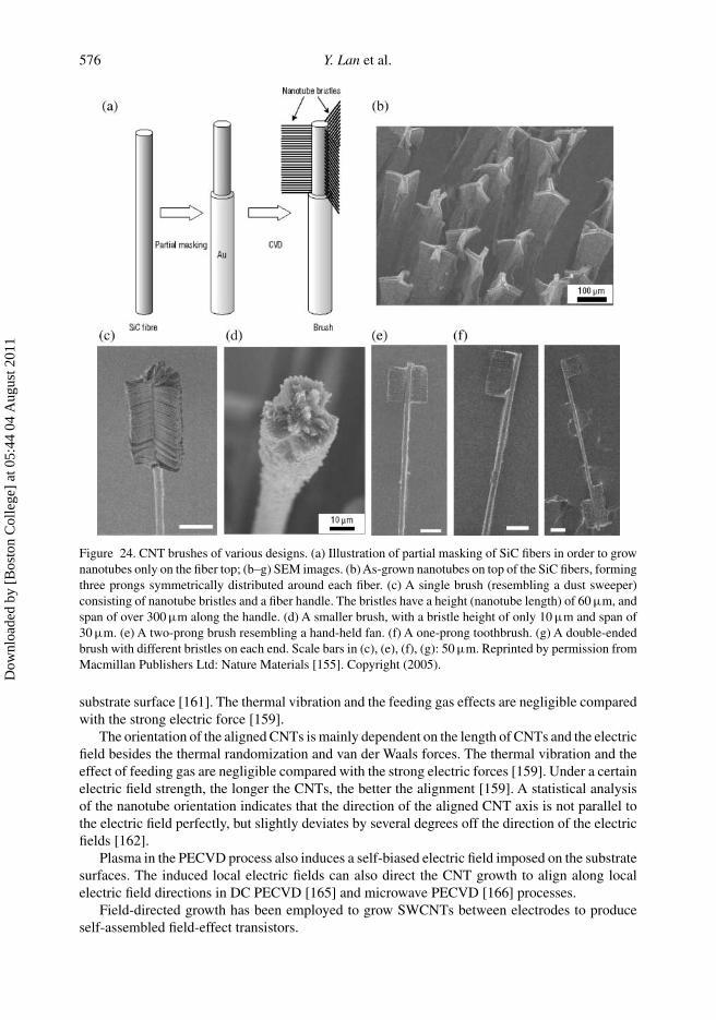
Figure 24. CNT brushes of various designs. (a) Illustration of partial masking of SiC fibers in order to grownanotubes only on the fiber top; (b–g) SEM images. (b) As-grown nanotubes on top of the SiC fibers, formingthree prongs symmetrically distributed around each fiber. (c) A single brush (resembling a dust sweeper)consisting of nanotube bristles and a fiber handle. The bristles have a height (nanotube length) of 60 μm, andspan of over 300 μm along the handle. (d) A smaller brush, with a bristle height of only 10 μm and span of30 μm. (e) A two-prong brush resembling a hand-held fan. (f) A one-prong toothbrush. (g) A double-endedbrush with different bristles on each end. Scale bars in (c), (e), (f), (g): 50 μm. Reprinted by permission fromMacmillan Publishers Ltd: Nature Materials [155]. Copyright (2005).
substrate surface [161]. The thermal vibration and the feeding gas effects are negligible comparedwith the strong electric force [159].
The orientation of the aligned CNTs is mainly dependent on the length of CNTs and the electricfield besides the thermal randomization and van der Waals forces. The thermal vibration and theeffect of feeding gas are negligible compared with the strong electric forces [159]. Under a certainelectric field strength, the longer the CNTs, the better the alignment [159]. A statistical analysisof the nanotube orientation indicates that the direction of the aligned CNT axis is not parallel tothe electric field perfectly, but slightly deviates by several degrees off the direction of the electricfields [162].
Plasma in the PECVD process also induces a self-biased electric field imposed on the substratesurfaces. The induced local electric fields can also direct the CNT growth to align along localelectric field directions in DC PECVD [165] and microwave PECVD [166] processes.
Field-directed growth has been employed to grow SWCNTs between electrodes to produceself-assembled field-effect transistors.
Dow
nloa
ded
by [
Bos
ton
Col
lege
] at
05:
44 0
4 A
ugus
t 201
1

Advances in Physics 577
Figure 25. (a) SEM image showing a 2D array of CNT pillars, each made of eight stacks of aligned nan-otube layers. Eight separate growth sequences (CVD steps) were used to grow the eight stack pillars. (b)High-magnification SEM image showing the interfaces (positions indicated by arrows) between the separatestacks of nanotubes in a single pillar. The stacks are numbered 1 to 8, corresponding to the first to the eighthstack grown sequentially. Reprinted with permission from X. Li et al., Nano Letters, 5, pp. 1997–2000,2005 [157]. Copyright (2005) American Chemical Society.
Attempts to organize CNTs into 2D crossbar structures by electric field-directed growth intwo dimensions have also been carried out [167,168]. The crossbar structure of CNT alignmentis hard to obtain only through electric fields. Usually, CNT crossbar architectures are achievedby combining field-directed growth with surface-directed growth [169] (see Section 2.1.5.4). 2DSWCNTs have successfully been produced along faceted nanosteps and along electric field inCVD growth. The electric field-directed CNTs are perpendicular to the surface-directed CNTs.The two alignment mechanisms take place simultaneously, producing dense nanotube grids.
2.1.3. Vertically aligned CNT arrays by PECVD
CNT arrays have been in situ fabricated more successfully by the PECVD method. The CNTarrays in situ aligned vertically were first synthesized using DC-PECVD [32,170–172]. Latera variety of PECVD methods, such as RF-PECVD, hot-filament PECVD, microwave PECVD,electron cyclotron PECVD, etc., are developed to grow aligned CNTs. DC-PECVD is discussed in
Dow
nloa
ded
by [
Bos
ton
Col
lege
] at
05:
44 0
4 A
ugus
t 201
1

578 Y. Lan et al.
Figure 26. The electric field-directed SWCNTs. (a) E = 0V/μm and (b) E = 0.5V/μm (inset: force appliedon a CNT in an electric field). Reprinted with permission from Y. Zhang et al., Applied Physics Letters, 79,pp. 3155–3157, 2001 [159]. Copyright (2001), American Institute of Physics.
detail in Section 3, including the experimental setup and experimental conditions. Other PECVDmethods are largely similar to the DC-PECVD method.
In these PECVD processes, DC electric fields, radio-frequency electric fields, or microwavesproduce plasmas to primarily lower the synthesis temperature of CNTs. At the same time, anelectric field (DC or AC) is also produced over the substrate surface, directing the CNT growthsimilar to the electric field effect discussed in Section 2.1.2. The straight CNTs grow along thedirection of the parasitic electric field in the plasma [165,166].
Besides the CNT alignment along the plasma-induced electric field, CNTs can also be arrangedon the substrate surface to form 3D CNT arrays. The sites of catalytic nanoparticles are criticalto the location of CNTs on the substrate surface. Because the CNTs grow only from the catalyticnanoparticles in a PECVD process, the sites of catalytic nanoparticles determine spatial locationsof CNTs. So the preparation of catalytic nanoparticles is very important on the fabrication ofvertical CNT arrays of various patterns. Table 2 summarizes several methods for preparing catalyticnanoparticles.
2.1.3.1 One-dimensionally ordered CNT arrays Usually the PECVD-grown CNTs are one-dimensionally (1D) ordered: the aligned CNTs are vertical to the substrate surface, while the CNT
Table 2. Some preparation methods of catalytic nanoparticles.
Catalyst
Methods Position Size Site density Procedure Others
Solution method Random Several nanometers Simple, easy CheapSputtering deposition Random Controllable narrow Easy CheapElectrochemical deposition Random Narrow ControllablePhotolithography Controllable Controllable Controllable Time consuming ExpensiveMicrosphere lithography Controllable Controllable Controllable Less than three
patternse-beam Controllable Controllable Controllable ExpensiveMicro-stamp Controllable Controllable Controllable One pattern
Dow
nloa
ded
by [
Bos
ton
Col
lege
] at
05:
44 0
4 A
ugus
t 201
1

Advances in Physics 579
sites are random because of the random locations of catalytic nanoparticles on the substrate. Thecatalytic nanoparticles can be prepared by many methods, such as solution method [173–176],sputtering deposition [32,154,177], and electrochemical deposition [178]. The average number ofcatalytic nanoparticles per unit area can be controlled while the site locations of the nanoparticlesremain random on the substrate surface.
Solution method. Solution method is the simplest way for producing catalysts while also widelyemployed in preparing catalysts for various nanowire growths. Usually the substrate is soaked inthe catalytic compound, water or alcohol solution (such as NiNO3 solution), for several minutesand then dried at room temperature. The deposited ions or ion clusters work as catalysts. Insome cases, the deposited catalyst particles are reduced in hydrogen to activate their catalyticactivity. CNTs are grown from these catalysts. The catalysts prepared by the solution methodrandomly distribute on the substrate surfaces and the PECVD-grown CNTs are 1D ordered alongthe plasma-induced electric field.
For example, iron catalysts have been prepared by this method. Iron nanoclusters with diametersbetween 3 and 13 nm were synthesized in organic solvents by thermal decomposition of ironpentacarbonyl and then were deposited onto a silicon substrate [173]. Iron oxide nanoparticleswith diameters of 1–2 nm were synthesized by soaking silicon oxide substrates in a solution ofhydroxylamine and FeCl3 [174]. Iron catalysts were also prepared by the iron-storage protein,ferritin [175], and by the polystyrene-block-polyferrocenyldimethylesilane diblock copolymer[176]. 1D CNT arrays were successfully grown from these catalysts.
Sputtering deposition. Sputtering (magnetron) deposition is usually employed to coat thinfilms on substrates and now is one of the most commonly used methods to synthesize the surfacearrays of metal particles. The sputtered film is usually continuous at a thickness above 1 nm. Suchas-coated films are not good catalysts for CNT growth. However, the continuous films are alwayscoarsened into discrete nanoparticles under annealing or through a solid-state dewetting process.So-prepared nanoparticles are usually well capable of catalyzing the growth of CNTs.
The catalyst preparation procedure of sputtering is simple and effective to grow catalyticnanoparticles for the growth of vertically aligned CNTs [32,154,177]. Up to now, catalytic nanopar-ticles have been DC magnetron sputtered or radio frequency sputtered on substrates. Although thismethod is straightforward, it offers little control over the size or spacing of the metal nanoparticles,and patterned nanoparticle arrays are not achievable this way without additional modifications suchas templating.
In a typical DC magnetron sputtering process, substrates are cleaned in alcohol by ultra-sonication first, and then loaded into the sputtering chamber for catalyst film deposition. Thechamber is evacuated to a base pressure of 5 × 10⁻⁷ to 3 × 10⁻⁶ Torr. Then the pressure is main-tained at 3–6 mTorr by introducing Ar gas. The catalyst target is Ar+ bombarded for a few minutesto remove the oxidized surface layer on the target. Then the substrate temperature is maintainedat 0–300◦C during deposition. The sputtering normally takes a few seconds to about 20 min toachieve catalyst film thickness of 2–100 nm.
The thickness of the sputtered films is usually in the range of 2–100 nm. The as-deposited filmsare normally smooth and continuous.
In order to enhance the catalytic activity, the as-sputtered films are always annealed at hightemperature before CVD growth. The annealing is usually carried out in the same CVD chamberfor CNT growth. The catalyst-coated substrates are loaded into the chamber, then the chamber ispumped down to about 1 mTorr or less, followed by heating to several hundred Celsius degrees.If the catalyst films have been exposed to air, annealing in hydrogen may remove the oxidizedsurface layer on the catalyst films. Depending on the annealing temperature and time, the contin-uous film develops into many individual nanoparticles, as shown in Figure 27. Statistical analysisof nanoparticle sizes indicates the catalyst nanoparticle size increases linearly with the increase
Dow
nloa
ded
by [
Bos
ton
Col
lege
] at
05:
44 0
4 A
ugus
t 201
1
580 Y. Lan et al.
Figure 27. SEM photographs of Ni particles with varying thicknesses deposited using magnetron sputteringon 50 nm of SiO2 and then annealed at 750◦C in 20 Torr of H2 for 15 min. Reprinted with permission from M.Chhowalla et al., Journal of Applied Physics, 90, pp. 5308–5317, 2001 [179]. Copyright (2001), AmericanInstitute of Physics.
of the sputtered film thickness when it is below 100 nm, as theoretically predicted by Rayleighinstability theory.
Aligned CNTs are usually grown by PECVD methods immediately after the annealing step.During the PECVD growth, the plasma intensity should be well controlled for optimal results. Ifnot, those catalytic nanoparticles would either be quickly knocked off the substrate (over-etched)or agglomerate (over-heated) into bigger ones to survive.
In order to grow isolated aligned CNTs, discrete catalytic nanoparticles shown in Figure 28(c),not adjacent ones shown in Figure 28(a) and (b), are needed. Otherwise, more than one CNTs willgrow closely together forming CNT bundles as shown in Figure 28(d) and (e). In order to obtainuniform and isolated catalysts, the as-prepared catalysts can be pre-etched by a plasma beforeintroducing carbon sources.
Electrochemical deposition. Electrochemical deposition has been employed to prepare Ni[170,178,181], Ag [182–184], Au [184], and Pt [185] catalytic nanoparticles with different nucle-ation site densities and different particle diameters for CNT array growth. Similar to the catalystsprepared by the sputtering method, the electrochemically deposited nanoparticles are also ran-dom. The site density and diameter of catalytic nanoparticles can be adjusted straightforwardly.Compared with the sputtering methods, the electrochemically deposited metal nanoparticles couldhave a lower site density, smaller sizes, more uniform diameters, and can be well controlled. ForNi catalytic nanoparticles, the site density can be easily tuned between about 106 and 108 cm−2
and the diameter can be finely tuned from less than 50 nm up to 200 nm [178,186]. Figure 29shows the CNTs with different site densities from different catalytic site densities.
The electrochemical deposition of catalytic nanoparticles is a cheap, effective technique, and isscalable to tens of inches in surface distribution dimension. The CNT arrays grown from catalystsprepared by electrochemical deposition are therefore also inexpensive and scalable although theCNTs are randomly arranged on the substrate surface.
Dow
nloa
ded
by [
Bos
ton
Col
lege
] at
05:
44 0
4 A
ugus
t 201
1

Advances in Physics 581
Figure 28. Formation of (a) multiple, (b) double, and (c) single Ni catalytic nanoparticles on a substrateand subsequent growth of (d) multiple, (e) double, and (f) single vertical MWCNTs from the catalyticnanoparticles shown in (a)–(c), respectively. Reprinted with permission from V.I. Merkulov, Applied PhysicsLetters, 76, pp. 3555–3557, 2000 [180]. Copyright (2000), American Institute of Physics.
2.1.3.2 Three-dimensionally ordered CNT arrays In order to synthesize 3D ordered CNTs,2D ordered catalytic nanoparticles are required. The 2D ordered catalytic nanoparticles canbe prepared by photolithography, X-ray photolithography, e-beam lithography [36,187], micro-sphere lithography, anodized aluminum oxide (AAO) templating [141,188,189], and micro-stampmethod [190]. Among them, the microsphere lithography technique is a simple, cheap, and effec-tive method to produce 2D ordered catalytic nanoparticles in inch-scale. After the 2D catalyticnanoparticles are prepared, the CNTs are vertically grown from them using PECVD method toform 3D CNT arrays.
Microsphere lithography. Microsphere lithography has been proved to be a very simple,economic, and effective technique to fabricate large-scale nanoparticle arrays with long-rangeperiodicity [34,35,191–194]. It utilizes submicron latex beads hexagonally arranged into a mono-layer as a shadow mask for the following evaporation of various materials. As-deposited catalyticnanoparticles have a quasi-triangular shape, caused by the aperture shape in the microspheres
Dow
nloa
ded
by [
Bos
ton
Col
lege
] at
05:
44 0
4 A
ugus
t 201
1

582 Y. Lan et al.
Figure 29. SEM images of CNT arrays grown on Ni nanoparticles deposited electrochemically with a sitedensity of (a) 7.5 × 105 cm−2, (b) 2 × 106 cm−2, (c) 6 × 106 cm−2, (d) 2 × 107 cm−2, (e) 3 × 108 cm−2,and (f) a freestanding CNT. Reprinted with permission from Y. Tu et al., Applied Physics Letters, 80,pp. 4018–4020, 2002 [178]. Copyright (2002), American Institute of Physics.
mask, and their size is tunable by the use of different sphere diameters. The technique has beenused to prepare 2D catalytic nanoparticles to grow 3D CNT arrays [34,35], to prepare 2D orderedcatalyst patterns for ZnO nanorod arrays [195], and to grow TiO2 nanobowl arrays [196].
The microsphere lithography process involves three main steps [191,193,195]. Firstly, a 2Dself-assembled and periodically ordered monolayer of microspheres is formed on a substratesurface (Figure 30(a)). Several drops of the microsphere suspension are applied to the surfaceof a substrate and then spread using a pipette tip. After being held stationary for about 1 min toobtain good dispersion of the suspension, the substrate is then slowly immersed into a pond ofdeionized water. Once the microsphere-coated surface is immersed, microspheres lift off from thesubstrate and form an unordered monolayer floating on the water surface. Then, a few drops of2% dodecylsodiumsulfate solution are added to the water surface to change the surface tension(surface tension of water is 72.8 dynes/cm2 at 20◦C, while that of sodium dodecylsulfate solutionis 40–70 dynes/cm2 [197]). After the surface tension is reduced, all microspheres immediatelyassemble into a close-packed monolayer. At the same time, the monolayer is pushed aside dueto the change in the surface tension. The prior substrate is then removed through a clear area.Then the microsphere monolayer is picked up by another clean substrate that is then slowly dried.
Dow
nloa
ded
by [
Bos
ton
Col
lege
] at
05:
44 0
4 A
ugus
t 201
1

Advances in Physics 583
Figure 30. Highly ordered monolayer of polystyrene microspheres (diameter 0.5 μm) on a Si substrate madeby the self-assembly microsphere lithography. (a)AFM image of the closely packed hexagonal microspheres.(b) Optical image of a Si substrate coated with microspheres. Reprinted with permission from K. Kempaet al., Nano Letters, 3, pp. 13–18, 2003 [35]. Copyright (2003) American Chemical Society.
Figure 30(a) shows a monolayer of polystyrene microspheres deposited on a 10 mm × 10 mm Sisubstrate. The uniform diffraction color in Figure 30(b) shows that the coated microspheres areindeed highly ordered without major defects over a long distance. This is further confirmed by afast Fourier transform analysis. The area of a single domain can reach a few square centimeters.
Secondly, the microsphere monolayer is subsequently used as a shadow mask for physicalvapor deposition of the catalyst (Fe, Co, or Ni). During this deposition process, the metal vaporcan go through apertures in hexagonally packed microspheres leading to a honeycomb latticearray of quasi-triangular particles. Various deposition techniques such as e-beam lithography,magnetron sputtering, and thermal evaporation can be used to deposit metal catalysts throughthe microspheres. During a sputtered process, the isotropic velocity of the adatoms results incatalysts covering all opening areas, even beneath the microspheres. Therefore, after removingthe microspheres, the sputtering technique usually produces a honeycomb-like catalyst network.During a thermal evaporation process, the deposition is line-of-site and the catalytic material is onlydeposited onto the areas of the substrate that are not shadowed vertically by the microspheres.Aftermask removal, a highly ordered hexagonal array of catalyst particles is formed on the substrate.
Thirdly, the microspheres are chemically etched away in toluene or tetrahydrofuran or mechan-ically by ultrasonication, leaving a patterned catalyst array on the substrate surface. Figure 31(a)
Figure 31. (a) SEM image of honeycomb array of nickel catalytic particles evaporated through the 980 nmdiameter microsphere mask. (b) SEM image of the 45◦ tilted view of the honeycomb array of aligned CNTsgrown on the nickel particle array shown in (a). Reprinted with permission from J. Rybczynski et al., AppliedPhysics Letters, 88, p. 203122, 2006 [192]. Copyright (2006), American Institute of Physics.
Dow
nloa
ded
by [
Bos
ton
Col
lege
] at
05:
44 0
4 A
ugus
t 201
1

584 Y. Lan et al.
shows the triangular particles exposed after microsphere mask removal. The inter-particle spacingcan be adjusted by adopting microspheres of different diameters.
After the 2D catalyst arrays are prepared, 3D ordered CNT arrays can be grown from themusing PECVD methods, as shown in Figure 31(b).
2.1.4. Thermal CVD growth under gas flow fields
When CNTs grow at high temperatures, a feeding gas mixture (including reactive gases such asC2H4 and carrying gases such as H2) passes over the growing CNTs. The feeding gas produces aflow field, causing CNTs to move along the direction of the gas flow. So the flow field caused bythe feeding gas can orient the CNTs along the flow direction.
There are two key components in the alignment mechanism. Firstly, the growing fronts ofnanotubes should be free above the substrate surface. This may happen due to buoyant effect or byfast-heating method, or at elevated sites over the substrate ground-level surface. Secondly, thereshould be a gas flow field to direct the CNT growth. A flow field always exists in the CNT growthprocessing by CVD. Once the flow gas can carry CNTs (or their growing fronts) to overcomegravity, CNTs will grow along the gas flow direction.
2.1.4.1 Fast heating under high gas flow The flow-directed method is first employed to orientCNTs in a fast-heating CVD process [198–201]. Si wafer substrates with catalysts were heatedquickly to the reaction temperature in a CVD reaction chamber. Some resulting CNTs are longand oriented, while the short ones are random in orientation. The orientation of the long nanotubesis controlled by the gas flow direction.
It is believed that the fast-heating process causes a convection of the gas flow due to thetemperature difference between the substrate and the feed gas. Such a convection flow of the feedgas lifts the nanotubes upward and keeps them floating and waving in the feed gas until CNTs arecaught by the substrate because of van der Waals forces. During the whole growth process, thenanotubes are floating in the feed gas and growing along the gas flow direction.
In the fast-heating growth process, the flow rate is typically about 1000 sccm [201]. Such ahigh-rate flow would cause local flow turbulences. The stability of the gas flow depends on theinner diameter φ of the quartz tube of the CVD furnace and the gas flow speed ν, and can becharacterized by the Reynolds number Re = ρvφ/γ , where ρ is the density and γ the viscositycoefficient of the feed gas. The turbulent flow causes some CNTs to touch the substrate surface andterminates the CNT growth, producing short CNTs. The long CNTs are well oriented along theflow direction. So the synthesized CNTs in a fast-heating growth usually consist of well-orientedlong CNTs and short ones that are randomly oriented as shown in Figure 32(a) [198]. At a higherReynolds number, such as in the case of a large-diameter quartz tube and a high flow rate, relativelyshort and disordered CNTs are produced [202].
In order to grow long CNTs with alignment, a stable laminar gas flow is required to stabilizethe catalytic tip of the growing CNTs, making CNT tips travel longer distances over the substratesurface. When using a small-diameter quartz tube and a low flow rate (such as less than 200 sccm),the Reynolds number can be reduced down to 50, near the lower limit of conventional laminarflow ranges. Better aligned CNTs can be achieved at low laminar flow rates (Figure 32(b)). Stablelaminar flows with low Reynolds numbers are favorable for growing aligned CNT arrays [202].
The catalyst also affects the alignment of CNTs. It is reported that high-quality horizontallyaligned SWCNT arrays can be prepared when Cu is used as the catalyst (Figure 32(c)) [203].
2.1.4.2 Buoyant effect at low gas flow When a feeding gas reaches the center region of aquartz tube from the relatively cooler end during CVD growth, a temperature difference between
Dow
nloa
ded
by [
Bos
ton
Col
lege
] at
05:
44 0
4 A
ugus
t 201
1
Advances in Physics 585
Figure 32. SEM image of long CNTs oriented in a flow field. (a) SWCNTs grown under laminar flow ranges(Reynolds number = 50–2000). (b) MWCNTs grown at Reynolds number of 50. (c) SWCNTs grown fromCu catalysts. (a) Reprinted with permission from S. Huang et al., The Journal of Physical Chemistry B, 107,pp. 13251–13254, 2003 [198]. Copyright (2003) American Chemical Society. (b) Reprinted with permissionfrom B.H. Hong et al., Journal of the American Chemical Society, 127, pp. 15336–15337, 2005 [202].Copyright (2005) American Chemical Society. (c) Reprinted with permission from W. Zhou et al., NanoLetters, 6, pp. 2987–2990, 2006 [203]. Copyright (2006) American Chemical Society.
the substrate surface and the nearby gas will generate a vertical gas density difference (buoyanteffect). The buoyant effect of convection flow induced by such gas density gradient can lift theCNTs up above the substrate, and the growth direction of CNTs can then be guided by a shearflow near the substrate surface [204].
When the gas velocity is sufficiently low, the buoyant force will dominate. Figure 33 shows anSEM image of CNT arrays aligned by the buoyant effect. The CNTs are well aligned in parallelarrays. In order to improve the stability of the feed gas, the Reynolds number is decreased to below1.0 by employing a very low gas flow rate and a narrow CVD quartz tube [204].
2.1.4.3 Trench structure The CNTs can also be oriented by a gas flow without a lift forcewhen the catalysts are deposited on a high platform fabricated on a substrate surface [205,206].Figure 34(a) shows a microtrench substrate surface structure. Catalytic nanoparticles are depositedon top of the trench. During growth, the nanotubes are freely suspended over the substrate surfaceand oriented along the flow direction. When CNTs grow long enough, they would touch anothermicrotrench (Figure 34(b)) or settle down to the substrate surface due to gravity.
Figure 33. SEM image of SWCNT arrays obtained with 0.5 sccm of CH4 and 1.0 sccm of H2 at 970◦C.Reynolds number is 0.76 during CNT growth. Reprinted with permission from Z. Jin et al., Nano Letters, 7,pp. 2073–2079, 2007 [204]. Copyright (2007) American Chemical Society.
Dow
nloa
ded
by [
Bos
ton
Col
lege
] at
05:
44 0
4 A
ugus
t 201
1

586 Y. Lan et al.
Figure 34. A CNT array grown from trench structure. (a) Schematic drawing of nanotube growth fromelevated catalyst sites. (b) An SEM image of initial and terminal points of long nanotubes. Scale bar:50 μm. Reprinted with permission from Z.Yu et al., Chemistry of Materials, 16, pp. 3414–3416, 2004 [206].Copyright (2004) American Chemical Society.
The key point of the method is to elevate the catalytic site. The catalysts can be deposited ontop of the micotreches fabricated by photolithography [205,206]. A slight tilting of the substratealso raises the catalysts. Long and oriented CNTs grow in the gas flow direction from the substrateedge when a laminar flow dominates the growth dynamics inside the CVD reaction tube [207].The laminar flow is also important in the growth process. If turbulent flow occurs, the CNTs wouldgrow short and randomly, as observed in the fast-heating method. Depending on the experimentalconditions, the flow rate can be 1200 sccm [206], 60–300 sccm [207], or much lower (6 sccm) [204].
In some cases, the catalytic patterns produced by photolithography works similarly andSWCNTs are horizontally aligned between patterns [208].
Compared with other methods, CNTs grown in a gas flow are not only well oriented, but alsofrequently exceptionally long (in centimeters). So the method has also been used to grow longSWCNTs [202,203].
2.1.4.4 Two-dimensional CNT networks When a multi-step growth is carried out, crossed CNTarrays can be produced using the flow method. Figure 35 shows an SEM image of crossed nanotubearrays grown by a two-step growth process. The CNTs are grown first along one direction undera flow field. Then catalysts are deposited on the substrate and the substrate is rotated 90◦ to growanother CNT array in a perpendicular direction.
Combined with the epitaxy technique (Section 2.1.5.1–2.1.5.3), 2D crossed CNT arrays canbe synthesized by a one-step CVD procedure, as discussed in Section 2.1.5.4.
Figure 35. An SEM image of a 2D nanotube network grown by multistep growth in a flow field. Reprintedwith permission from S. Huang et al., Journal of the American Chemical Society, 125, pp. 5636–5637,2003 [199]. Copyright (2003) American Chemical Society.
Dow
nloa
ded
by [
Bos
ton
Col
lege
] at
05:
44 0
4 A
ugus
t 201
1

Advances in Physics 587
Figure 36. (a) An SEM image of SWCNTs grown in direction [1101] on R-plane sapphire substrate. Scalebar is 20 μm. (b) Simulation of the surface structure of the oxygen-depleted R-plane sapphire. The red andgray atoms indicate Al and O, respectively. The blue arrows indicate the direction [1101]. Reprinted withpermission from Q. Yu et al., The Journal of Physical Chemistry B, 110, pp. 22676–22680, 2006 [214].Copyright (2006) American Chemical Society.
2.1.5. Thermal CVD growth with epitaxy
Epitaxy is another promising approach to align CNTs horizontally. There are three differenttypes of epitaxial growth of CNTs [209]: lattice-directed epitaxy by atomic rows, taking place onatomically flat surfaces; ledge-directed epitaxy by atomic steps, taking place on vicinal surfaces;and graphoepitaxy by nanofacets, taking place on nanostructured surfaces.
2.1.5.1 Lattice-directed growth The lattice-directed growth of CNTs were observed along thelow-index directions of Si (100) [210], Si (111) [210],Au (111) [211], and 6H-SiC (0001) [212,213]surfaces. The synthesized CNTs are usually short. Later, long SWCNTs are aligned in parallelhorizontally on R-plane [214–217] and a-plane [217,218] sapphire.
In the lattice-directed growth, sapphire without intentional miscut (less than 0.5◦) is usuallyused as the substrate. SWCNTs grow on atomically flat surfaces. Figure 36(a) shows SWCNTsgrown on an R-plane sapphire surface. SWCNTs are aligned in parallel to the [1101]-direction.It is believed that the original surface layer of O atoms of the sapphire substrate may be depletedin the CVD process leaving the surface terminated by Al atoms, as shown in Figure 36(b). Inthis case, [1101] becomes the direction of the compact arrangement of Al atoms on the sapphiresurface and the arrangement of Al atoms builds the pseudo-one-dimensional arrays, shown as aseries of grooves aligned in the direction [1101] in Figure 36(b). The CNTs usually grow along theunique 1D array of surface atoms [217,219,220]. It is observed that SWCNTs are aligned alongthe [1100]-direction on (1120) a-plane [218,221] or along the [1101]-direction on (1102) R-planesapphire [214,215,219]. The preferential growth of SWCNTs along these lattice directions wasattributed to higher charge densities along these atomic rows due to electrostatic and van der Waalsforces.
Lattice-directed epitaxial growth of SWCNTs also takes place on other atomically flat single-crystal substrates. Recently, for instance, SWCNTs were observed to grow on MgO (001)preferentially along the [110] and [110] directions, and on single-crystal quartz [220,222].
2.1.5.2 Ledge-directed growth The formation of highly aligned and dense arrays of long SWC-NTs was first observed on c-plane sapphires in a CVD process [223]. The c-plane sapphire wafersturned out to have a miscut of a few degrees off the c-plane to produce atomic steps of the vicinalα-Al2O3 (0001) surfaces (Figure 37(a) and (b)). The atomic steps, with a height equal to one-sixthof the hexagonal unit cell (h = c/6 = 0.219 nm), follow a general direction perpendicular to themiscut direction (Figure 37(b)). Their average spacing is d = h/ sin θ , where θ is the miscut incli-nation. CNTs grow along the atomic steps of the vicinal α-Al2O3 (0001) surfaces and form highlyaligned dense arrays (Figure 37(c)).
Dow
nloa
ded
by [
Bos
ton
Col
lege
] at
05:
44 0
4 A
ugus
t 201
1
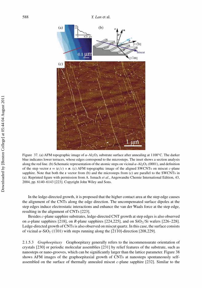
588 Y. Lan et al.
Figure 37. (a) AFM topographic image of α-Al2O3 substrate surface after annealing at 1100◦C. The darkerblue indicates lower terraces, whose edges correspond to the microsteps. The inset shows a section analysisalong the red line. (b) Schematic representation of the atomic steps on vicinal α-Al2O3 (0001), and definitionof the step vector s = (c/c) × n. (c) AFM topographic image of the aligned SWCNTs on miscut c-planesapphire. Note that both the s vector from (b) and the microsteps from (c) are parallel to the SWCNTs in(a). Reprinted figure with permission from A. Ismach et al., Angewandte Chemie International Edition, 43,2004, pp. 6140–6143 [223]. Copyright John Wiley and Sons.
In the ledge-directed growth, it is proposed that the higher contact area at the step edge causesthe alignment of the CNTs along the edge direction. The uncompensated surface dipoles at thestep edges induce electrostatic interactions and enhance the van der Waals force at the step edge,resulting in the alignment of CNTs [223].
Besides c-plane sapphire substrates, ledge-directed CNT growth at step edges is also observedon a-plane sapphires [218], on R-plane sapphires [224,225], and on SiO2/Si wafers [226–228].Ledge-directed growth of CNTs is also observed on miscut quartz. In this case, the surface consistsof vicinal α-SiO2 (1101) with steps running along the [2110]-direction [208,229].
2.1.5.3 Graphoepitaxy Graphoepitaxy generally refers to the incommensurate orientation ofcrystals [230] or periodic molecular assemblies [231] by relief features of the substrate, such asnanosteps or nano-grooves, which can be significantly larger than the lattice parameter. Figure 38shows AFM images of the graphoepitaxial growth of CNTs at nanosteps spontaneously self-assembled on the surface of thermally annealed miscut c-plane sapphire [232]. Similar to the
Dow
nloa
ded
by [
Bos
ton
Col
lege
] at
05:
44 0
4 A
ugus
t 201
1

Advances in Physics 589
Figure 38. Graphoepitaxial SWCNT growth on different annealed miscut c-plane sapphire substrates. (a)SEM image of straight nanosteps along [1010]. (b) AFM image of CNTs grown on the nanosteps along[1010]. (c) Nanosteps along [1120] and (d) the highly faceted sawtooth-shaped nanosteps along [1010].Insets: the possible morphologies of CNTs grown along the faceted nanosteps of sapphire substrates. Thewhite arrows in (c) and (d) mark the grown CNTs. Reprinted with permission from A. Ismach et al., Journalof the American Chemical Society, 127, pp. 1110–1116, 2005 [230]. Copyright (2005) American ChemicalSociety.
miscut of c-plane sapphire [223], wafers are miscut and mechanically polished to produce atomicsteps toward the [1100] or [1210] directions with a height of h = c/6 = 0.21 nm (Figure 37(b)).The substrates were then thermally annealed at high temperature. Upon annealing, the thermo-dynamically unstable atomic steps tend to reduce the surface energy by bunching atomic stepstogether into faceted nanosteps spaced by flat c-plane terraces. The height of the nanosteps isbetween one and three times larger than the unit cell, i.e., 1.3–3.8 nm. The atomic steps along[1120] can bunch into stable R-faceted nanosteps (inset in Figure 38(c)) and the CNTs grow onthis surface graphoepitaxially to form CNT arrays along the [1120]-direction (Figure 38(c)).
The atomic steps along [1010] initially bunch into metastable P-faceted nanosteps (inset inFigure 38(a)), which leads to graphoepitaxial nanotube growth along [1010] (Figure 38(b)). Uponfurther annealing, the metastable P-faceted nanosteps break into sawtooth-shaped S-/R-bifacetednanosteps (inset in Figure 38(d)) and graphoepitaxy produces nanotubes loosely conformal toalternate S and R facets along [1120] and [2110], respectively, as shown in Figure 38(d).
Using artificial nanosteps, SWCNTs can also be horizontally aligned on other substrates. Forexample, plasma treatment creates some steps with several nanometers height on Si/SiO2 wafersurfaces. SWCNTs with a site density of 3–8 tubes/μm can be horizontally aligned on suchsubstrate surfaces [226]. SWCNTs can also be directly aligned along the trenches created byelectron beam lithography on SiO2/Si substrates [227], or along the patterned steps of sapphire[224]. Different from the flow-directed growth where CNTs are grown across the trenches, herethe CNTs are grown along the trenches.
Dow
nloa
ded
by [
Bos
ton
Col
lege
] at
05:
44 0
4 A
ugus
t 201
1

590 Y. Lan et al.
Figure 39. Orthogonal self-assembly of SWCNT crossbar architectures by simultaneous graphoepitaxyand field-directed growth in a one-step CVD procedure. (a) Schematic representation of the orthogo-nal self-assembly. (b) SEM image of a dense SWCNT grid obtained by simultaneous graphoepitaxy andfield-directed growth. Reprinted with permission from A. Ismach and E. Joselevich, Nano Letters, 6, pp.1706–1710, 2006 [169]. Copyright (2006) American Chemical Society.
2.1.5.4 Two-dimensional CNT networks Combinations of the CNT epitaxial growth with thefield-directed growth (Section 2.1.2) or flow-directed growth (Section 2.1.4) can produce 2Dcrossbar arrays of CNTs in a one-step CVD procedure.
Figure 39 shows a crossbar array of SWCNTs spontaneously produced in a one-step CVDprocedure by simultaneous graphoepitaxy and field-directed growth, perpendicular to each other.The miscut c-plane sapphire is annealed to produce the nanosteps along the [1120]-direction,while an electric field is applied perpendicularly to the nanosteps. The nanotubes originating fromcatalyst nanoparticles lying on the sapphire grow along the faceted nanosteps, while the nanotubesemerging from the catalyst on patterned amorphous SiO2 stripes grow freely without interactingwith the surface, in a way that allows their alignment by the electric field, eventually falling acrossthe nanotubes previously grown on the sapphire. SWCNTs grow along the atomic steps of miscutc-plane sapphire surfaces [223], or along the 1.3–4 nm high-faceted nanosteps of annealed miscutc-pane sapphire [232]. The alignment of the graphoepitaxial SWCNTs is unaffected by externalforces, such as electric field and gas flow field [223,232]. So the nanotubes originating from thecatalyst nanoparticles lying on the bare sapphire grow along the nanosteps, while the nanotubesoriginating from catalyst nanoparticles lying on the amorphous SiO2 islands grow up freely and arealigned by the electric field perpendicular to the nanosteps. The two alignment mechanisms takeplace selectively on miscut c-plane sapphire and patterned amorphous SiO2 strips, respectively,without mutual interference, producing dense nanotube grids.
Similar to the combination of lattice-directed growth and electric field-directed growth, 2Dcrossbar structured CNTs can also be produced in a one-step CVD process from a combinationof lattice-directed growth and flow-directed growth [233]. Figure 40 shows the mechanism andSEM images of SWCNT crossbar structures grown on quartz substrates in this way. The averagelength of lattice-orientated SWCNTs can reach hundreds of microns, and the spacing betweenthe nanotubes is about several microns. Gas flow-directed SWCNTs are millimeters long and thespacing between nanotubes can be reduced to about 10 μm. The CNT node density of the crossbarstructure is about 107 cm−2.
Combining lattice-directed growth and graphoepitaxial growth, bent CNTs can be horizon-tally grown on crystal substrates, like R-plane sapphire with artificial nanosteps [224]. SWCNTsfirst grow along the specific crystallographic [1101]-direction on R-plane sapphire due to thelattice-oriented growth and then grow along artificial nanosteps, perpendicular to the first SWCNT
Dow
nloa
ded
by [
Bos
ton
Col
lege
] at
05:
44 0
4 A
ugus
t 201
1

Advances in Physics 591
Figure 40. 2D CNT networks produced from a combination of lattice-directed growth and flow-directedgrowth. (a) Illustration of the mechanism for the growth of crossbar structured CNTs based on lattice-directedand flow-directed growth. (b) SEM image of SWCNT crossbar structure on quartz. Reprinted with permissionfrom B. Zhang et al., The Journal of Physical Chemistry C, 113, pp. 5341–5344, 2009 [233]. Copyright (2009)American Chemical Society.
growth direction [1101]. These nanosteps change the nanotube growth direction from [1101] tothe nanostep direction with the bending angle of nearly 90◦.
2.1.6. Thermal CVD under magnetic fields
Another approach to align CNTs is to control the orientation of catalyst nanoparticles [234,235].Ferromagnetic materials, such as iron, nickel, and cobalt, have been used for CNT catalysts andhave one crystallographic magnetic easy axis. The magnetic easy axis tends to be parallel tothe magnetic field. As a result, an applied magnetic force can orient these magnetic catalyticnanoparticles, like catalytic iron nanoparticles [234] and Fe3O4 nanoparticles [235]. Because onlya certain nanocrystalline facet of catalytic nanoparticles is catalytically active and the diffusion rateof carbon atoms on the facet is the highest (such as (220) of Ni) [165,236], the CNTs preferentiallygrow from the certain facet of the catalytic nanoparticles and the grown CNTs are oriented at acertain angle. Figure 41 shows the histogram distribution of CNTs synthesized with or withoutan external magnetic field. When a magnetic field is applied during the CNT growth, CNT growpreferentially along two certain directions.
2.2. Ex situ techniques for CNT alignment
Ex situ assembly of CNTs is a post-synthesis method for CNT alignment. CNTs are first synthe-sized by CVD or other methods, and then are assembled by electric fields, magnetic fields, forcefields, or other methods. Compared with the in situ techniques, the ex situ techniques are free ofcollateral growth restrictions such as substrate material and growth temperature.
2.2.1. Electric fields
CNTs can be aligned under electric fields in liquids [237–240]. The electric fields can be DC or ACfields. Figure 42 shows SEM images of aligned CNTs between two electrodes. Gold interdigitatedelectrodes are fabricated by vacuum deposition on Si/SiO2 substrates. Then the substrates areimmersed in the SWCNT suspension and an electric field is generated between the electrodes[237]. The CNTs are polarized in the suspension by the electric field because of dielectric mismatchbetween CNTs and the liquid. The polarization moment rotates the CNTs toward the direction ofelectric field lines, therefore aligning them in a common direction. After being aligned, the CNTsare taken out with the substrates and dried in air.
Dow
nloa
ded
by [
Bos
ton
Col
lege
] at
05:
44 0
4 A
ugus
t 201
1

592 Y. Lan et al.
Figure 41. (a) Histogram distribution of CNTs obtained by analyzing as-synthesized CNT growth angles inthe presence of a magnetic field. The histogram displays two preferred growth directions centering at 60◦and 130◦. (b) Histogram distribution attained by analyzing as-synthesized CNT growth angles prepared inthe absence of a magnetic field. No preferential growth angle is observable from these samples. Reprintedwith permission from N. Kumar et al., Applied Physics Letters, 86, p. 173101, 2005 [235]. Copyright (2005),American Institute of Physics.
Figure 42. SEM images of the SWCNTs aligned under AC electric fields. (a) Aligned by applying an ACelectric field with a frequency of 5 MHz and a voltage of 10V peak to peak. (b) Aligned by applying anAC electric field with a frequency of 500 Hz and a voltage of 10V peak to peak. Reprinted with permissionfrom X.Q. Chen et al., Applied Physics letters, 78, pp. 3714–3716, 2001 [237]. Copyright (2001), AmericanInstitute of Physics.
Another approach to align random CNTs, also related to electric-field-directed alignment, isthe orientationally selective ablation of random networks with a planarly polarized laser [241].SWCNTs oriented with a projection in the plane of polarization were selectively ablated, leavingon the surface only those that are oriented perpendicular to the plane of polarization.
2.2.2. Magnetic fields
Calculations reveal that CNTs exhibit diamagnetic or paramagnetic responses depending on themagnetic field direction, the helicity of CNTs, the Fermi energy of CNTs, and the radius [101].Metallic SWCNTs are paramagnetic in the direction of their long axes, confirmed by experimental
Dow
nloa
ded
by [
Bos
ton
Col
lege
] at
05:
44 0
4 A
ugus
t 201
1

Advances in Physics 593
Figure 43. (a) Field dependence of the magnetic moment of CNTs at high fields. The CNTs withdiameter of 2–10 nm are grown by arc-discharge technique. (b) Experimental setup to align CNTs inmagnetic fields. (c) Small-angle neutron scattering pattern of CNTs aligned in magnetic fields shown in (b).(a) Reprinted figure with permission from J. Heremans et al., Physical Review B 49, pp.15122–15125, 1994[242]. Copyright (1994) by the American Physical Society. (b) and (c) Reprinted figure with permissionfrom D.K. Yoon et al., Advanced Materials, 18, 2006, pp. 509–513 [243]. Copyright John Wiley and Sons.
data (Figure 43(a)). Under magnetic field B, the CNTs with magnetic dipole moment P receivea torque vector given by τ = P × B. At high magnetic fields, the magnetic force applied on theCNTs can align the whole CNTs along the magnetic field direction.
Usually CNTs are dispersed ultrasonically in a liquid epoxy resin and then the mixture is leftin a magnetic field at room temperature before it is cured (Figure 43(b)). The alignment of CNTsin the liquid under a magnetic field occurs due to the cooperative effect of the magnetic torqueexerted by the magnetic field directly on the nanotubes and the hydrodynamic torque and viscousshear (i.e., drag forces) exerted on the nanotubes by the polymer chains [244–248]. Small-angleneutron scattering of CNTs indicates that the CNTs really rotate and align in the magnetic field(Figure 43(c)). The calculation of SWCNT susceptibilities predicts that a field in the order of 10 Tcan produce an observable alignment in a liquid suspension of SWCNTs [249]. Transmitted lightmeasurement indicates that 90% of purified SWCNTs can be aligned in dimethylformamide alonga magnetic field (19 T) axis with a CNT axial orientation within 17 ± 1◦ [250]. The alignment
Dow
nloa
ded
by [
Bos
ton
Col
lege
] at
05:
44 0
4 A
ugus
t 201
1

594 Y. Lan et al.
energy from CNT susceptibility should be much higher (> 5κBT) to overcome the Brownianmotion with an average energy of κBT , where T is the experimental temperature. Additionally,X-ray diffraction experiments also confirm that CNTs can align along the magnetic field direction.
The as-synthesized CNTs are usually paramagnetic because of the entrapped catalytic nanopar-ticles in the CNTs [242,244]. The magnitude of magnetization of the as-synthesized CNTs istypically several orders of magnitude higher than the purified CNTs. Under a magnetic field, the as-synthesized CNTs also tend to align parallel to the external magnetic field. In order to increase thesusceptibility of individual CNTs, they may be coated or filled with magnetic nanoparticles [251].
2.2.3. Mechanical methods
CNTs can be effectively aligned by various mechanical methods. Below we briefly review thesemechanical methods.
2.2.3.1 Stretching method Stretching method is probably the simplest ex situ method to alignCNTs. CNTs are aligned under an external force field.
Figure 44 shows a simple stretching method to align CNTs on substrates. The CNTs are synthe-sized first on a substrate. The as-synthesized CNTs are random, tangled, and curved (Figure 44(a)).Once the substrate is broken in the middle, a force pulls the CNTs on the substrate and the CNTsare aligned (Figure 44(b)). The aligned CNTs are parallel to each other and perpendicular tothe crack.
CNTs are also aligned in polymers. The CNTs are first embedded in a polymer matrix, andaligned CNTs can be obtained by cutting thin slices of the CNT/polymer composites [253].The CNT composites are also casted into films and then cut into small strips. Mechanicallystretching the cast strips to a desired stretching ratio at high temperature aligns CNTs parallel tothe stretching direction [254]. 2D X-ray diffraction patterns indicate that the CNTs are alignedwith their longitudinal axes parallel to the stretching direction. The mechanical stretching methodhas been used to align SWCNTs in polymeric composite films [255,256].
Different from the force field produced by stretching, spinning produces a radial force field.When CNTs are dispersed in thermoplastic resins and melt-spun at high temperature, they can bewell aligned in the composite along the spinning direction [257].
Figure 44. (a) Thermal CVD-grown MWCNTs deposited on the substrate. The grown CNTs are curledand randomly distributed on substrate surface. (b) Aligned DWCNTs after being pulled out. The CNTs arestraight and parallel to the substrate surface. Reprinted from Chemical Physics Letters, 368, W.Z. Li et al.,pp. 299–306 [252]. Copyright (2003), with permission from Elsevier.
Dow
nloa
ded
by [
Bos
ton
Col
lege
] at
05:
44 0
4 A
ugus
t 201
1

Advances in Physics 595
Figure 45. MWCNT forest conversion into sheets and assemblies of those sheets. (a) Photograph of aself-supporting 3.4 cm-wide, meter-long MWCNT sheet that has been hand-drawn from a nanotube forest;it is transparent. (b) SEM image, at a 35◦ angle with respect to the forest plane, capturing an MWCNTforest being drawn into a sheet. (c) SEM micrograph showing the cooperative 90◦ rotation of MWCNTsin a forest to form a sheet. (d) SEM micrograph of a 2D reinforced structure fabricated by overlaying fournanotube sheets with a 45◦ shift in orientation between successive sheets. From M. Zhang et al., Science, 309,pp. 1215–1219, 2008 [258]. Reprinted with permission from AAAS.
The stretching method can macroscopically align the CNTs while not providing deterministiccontrol over individual CNT alignment or position during assembly. The direction of CNTs cannotbe aligned along the force field perfectly.
2.2.3.2 Spinning methods The spinning method has been successfully used to fabricate CNTropes and CNT clothes [258–263]. Figure 45 shows a CNT sheet assembled by a spinning method.The CNTs are well aligned along the force direction. The transparent thin CNT sheets are fabricatedin meters. This kind of nanosheets can be used for TEM grids (Section 5.1.2), incandescent displaysand lighting (Section 4.1.4), thermoacoustic loudspeakers (Section 5.3), etc.
Up to now, two main kinds of spinning methods, wet-spinning and dry-spinning, havebeen invented. In a wet-spinning process, the synthesized CNTs are dispersed in a melt or aliquid/solution, aligned by flow processing, and then converted into a fiber through cooling orsolvent removal [265]. The dry-spinning method directly spins the CNT forests synthesized byCVD [93], directly spins a CNT aerogel formed in the reaction zone [262], or spins cotton-likeraw CNTs to form CNT yarns or continuous fibers. Here we do not review these spinning methods
Dow
nloa
ded
by [
Bos
ton
Col
lege
] at
05:
44 0
4 A
ugus
t 201
1

596 Y. Lan et al.
in detail since there are already some thorough reviews on wet-spinning from solution [209,266],on dry-spinning [209,259], and on electrospinning from CNT composites [258].
2.2.4. Other ex situ methods
Besides the ex situ methods discussed above, CNTs can also be aligned by fluidic methods [97],electrophoresis [267,268], surface forces [269], surface acoustic waves [270], and by chemicallydirected assembly [271].
3. Direct-current PECVD
Probably the most widely used growth method for aligned CNTs is DC-PECVD due to its effec-tiveness in alignment control and equipment setup simplicity. It is, therefore, worth to dedicatethis section to review this technique in more thorough details while also not limiting the discus-sion to a single type of electrical discharge (plasma). Besides, comprehensive reviews on variousaspects of PECVD techniques for aligned CNT growth is already available [272,273]. Althoughit has been reported that, in DC configurations, CNTs can be grown under either a positive ornegative bias [274], the most popular choice is applying a negative bias on the substrate probablyto utilize the ion bombardment effects that will be discussed in the following paragraphs. Unlikein the cases of AC plasmas where identical parallel plate electrodes are predominantly used forgrowth uniformity, DC plasmas require a higher breakdown voltage to initiate and therefore theelectrode shapes need to be modified to facilitate the initiation. The simplest and most popularoption is to have the positive electrode of a much smaller effective surface area, e.g., a small plateor even a rod end with a flat or pointy tip, so that its local sharp edges can more easily inducestrong local electric fields to initiate the plasma. Besides, this configuration can also provide rel-atively uniform CNT growth over centimeter scales, sufficient for laboratory research. There arealso specific characteristics of DC plasma growth such as the substrate conductivity requirementand dark discharge plasma states, which will be demonstrated together with some general growthaspects in all PECVD processes.
3.1. Equipment setup and growth procedure
An exemplary schematic setup of the DC-PECVD apparatus is illustrated in Figure 46 [275]. Insidea vacuum chamber (1), a rod-shaped molybdenum anode (2) hangs vertically about 1–2 cm over
Figure 46. (a) Setup of DC-PECVD system [275]. (b) 3D structure of the growth chamber of alignedCNTs [57].
Dow
nloa
ded
by [
Bos
ton
Col
lege
] at
05:
44 0
4 A
ugus
t 201
1

Advances in Physics 597
a horizontal molybdenum cathode plate (3) which also serves as a sample stage. The diameters ofthe rod and the plate are 0.25′′ and 4′′, respectively. Underneath the cathode plate is a resistive plateheater (4) powered by an external AC voltage (5). The two electrodes are connected to an externalpower supply (6), MDX-1K Magnetron Drive (The Advanced Energy�), which runs on a constantvoltage, current or power mode. Feedstock gases are introduced into the chamber via a single gaspipe (7) after going through respective flow controllers (8, 9), and the chamber evacuation is solelyexecuted by a mechanical pump (10). The evacuation speed and therefore the system pressure aremanually controlled by a gate valve (11) which throttles the evacuation channel. In addition tothe basic structure in Figure 46, a pressure sensor is installed in the chamber base plate, and athermocouple is first insulated in a thin quartz tubing and then brought into contact to the cathodefor temperature monitoring. Compared to the other plasma sources which are mostlyAC, the majorsetup difference is that the anode surface is shrunk into a much smaller size than the cathode. Thismakes the sharp edges of the anode to be almost the closest geometrical point to the cathode wherethe plasma should initiate and the edges allow a relatively low breakdown voltage due to localfield enhancement.
The DC-PECVD process for vertically aligned CNT arrays includes four basic steps, namelyevacuation, heating, plasma generation, and cooling. A typical procedure can be described asfollows. After samples are loaded onto the sample stage, the chamber is evacuated to a basepressure of around 10−2 Torr. NH3 is then introduced into the chamber to reach a pressure of8 Torr and the heater is turned on to gradually elevate the stage temperature. Typical growthtemperatures used are in the range of 450–600◦C which can be normally reached in a period of15–30 min. The pressure is maintained by adjusting the aperture of the gate valve. As soon asthe temperature and pressure are stabilized, a DC bias voltage of 450–650V is applied to thegap between the two electrodes to ignite an electrical discharge (plasma) over the sample. Theplasma current intensity may typically vary within 0.1–0.5A. C2H2 is then introduced to trigger theCNT growth. The flow rate ratio of NH3:C2H2 is usually around 4:1 which results in a minimumamount of amorphous carbon formation. And the growth time may vary from a couple of minutesto hours depending on the growth rate and desired CNT length. When the end of growth time isreached, the bias voltage is removed immediately to terminate the plasma. Meanwhile, the gasesare discontinued and the gate valve is fully opened to evacuate the chamber. The heater is alsoturned off for the samples to cool down naturally. Inert gases such as N2 or Ar can also be fed intothe chamber to speed up the cooling process if desired.
Again, the above setup and procedure should be taken as a basic example with room forvariations in peripheral aspects such as triode-type electrode setups [274], different mechanismsfor substrate heating, and application of other reacting gases such as CH4 and H2. The apparatusand process simplicity has greatly facilitated the adoption of this technique by many researchgroups around the globe and has helped to push the aligned CNT research forward rapidly andsignificantly.
3.2. Substrate and underlayer
For any growth process of CNTs, the general requirements for the underlying substrate (or under-layer coated onto the substrate) are that (1) it has to be both physically and chemically stable forup to the growth temperature and (2) its surface must not poison the catalyst particles in contact(such as by forming an inactive alloy) which can be frequently avoided by an inert buffer layercoating. For PECVD processes, the substrate must also be chemically stable under the plasmawhich is rich of H-species. Some weakly bonded oxides such as indium oxide can be quicklyreduced in this plasma and is therefore usually not applicable as the substrate or underlayer. Andfor DC-PECVD, in particular, the substrate must be electrically conductive to sustain a continuous
Dow
nloa
ded
by [
Bos
ton
Col
lege
] at
05:
44 0
4 A
ugus
t 201
1

598 Y. Lan et al.
DC current flow through its surface where the CNTs grow from. Most metals and semiconduc-tors (such as silicon wafers) are very good substrate materials, and insulating substrates suchas glass [32] and polyimide [276] can be first coated with a conductive layer to work properly(requiring electrical contact of the conductive layer to the cathode during growth). Although ithas been reported [32] that directly depositing catalyst films onto glass may still result in alignedCNT growth, this phenomenon should be due to the formation of a conductive amorphous carbonlayer which connects the narrow spacing among the dewetted catalyst particles, which is moredirectly observed on polyimide substrates [276]. Indeed, large-spacing catalyst particles are foundto always require a conductive substrate or underlayer for CNT alignment. Common transparentconductive oxide (TCO) thin films can also be applied as conductive underlayers on insulatingglass substrates for aligned CNT growth by DC-PECVD, although it requires proper choice of thedischarge conditions [276], which will be discussed in detail later.
3.3. Growth temperature
One of the major advantages of using PECVD growth techniques is the low growth temperature.The ionization of the neutral hydrocarbon molecules inside the plasma facilitates the breaking ofthe C–H bonds and lowers the activation energy of the CNT growth. Indeed, the activation energyfor PECVD processes is experimentally measured to be ∼0.3 eV, much lower than the ∼1.2 eV forthermal CVD processes [277]. Figure 47 shows the extrapolated activation energy values for DC-PECVD and thermal CVD growth based on experimental data. DC-PECVD growth temperaturehas successfully been demonstrated to be as low as 390◦C for bamboo-like CNTs and 120◦C foramorphous CNFs [278], compared to CVD growth temperatures in the 500–700◦C range.
Although at very low temperatures the C-atoms in the grown structure begin to be moredisordered (Figure 48), the fact that C-atoms can still diffuse and precipitate along the catalystsurfaces to result in nanostructure growth demonstrates that carbon diffusivity is just the limiting
Figure 47.Arrhenius plots for CNT growth rates on different catalysts in NH3 diluted C2H2. Reprinted figurewith permission from S. Hofmann et al., Physical Review Letters 95, pp. 036101-036104, 2005 [277].Copyright (2005) by the American Physical Society.
Dow
nloa
ded
by [
Bos
ton
Col
lege
] at
05:
44 0
4 A
ugus
t 201
1

Advances in Physics 599
Figure 48. CNF PECVD deposited at (a, d) 500◦C, (b, e) 270◦C, and (c, f) 120◦C. (a)–(c) SEM imagesof CNF arrays and (d)–(f) HRTEM images of a CNF. Reprinted with permission from S. Hofmann et al.,Applied Physics Letters, 83, pp. 135–137, 2003 [278]. Copyright (2003), American Institute of Physics.
factor for low-temperature growth rate, whereas the feedstock hydrocarbon dissociation is reallythe bottleneck process for growth initiation. This understanding leads to remote-plasma CVDprocesses for growth temperature lowering [206,279], which is beyond the scope of this review.Since alignment can still be achieved at these low temperatures (Figure 48), many applicationopportunities open up, especially in templating on plastic substrates where temperature is sensitiveand morphology is more essential than crystallinity.
3.4. Plasma heating and etching effects
Although the primary intention to introduce plasma in CNT growth is to reduce the activationenergy by facilitating hydrocarbon dissociation as stated above, the plasma has two other majorcollateral effects which must be taken into consideration and sometimes utilization: heating andetching. As a DC voltage higher than the breakdown threshold on the Paschen curve is appliedacross the electrodes, free electrons are energized and subsequently ionize neutral species throughelastic collisions, generating more free electrons. Such an avalanche process causes an electricaldischarge state of a collection of free electrons, ions, and neutral species, which is called plasma.The collisions among energized charged particles and neutral molecules inside the plasma bodyraise the gas temperature which can be conducted to the substrate. Also the ionic bombardmentonto the substrate surface (sitting at a negative potential on the cathode) caused by positive ionsaccelerated across the plasma sheath field incurs ohmic heating of the substrate. Both processestogether can lead to significant substrate heating to above 700◦C in real growth chambers withouta separate heater [172]. Figure 49 shows that plasma heating can raise the substrate temperatureas much as using a separate heater. Aligned CNTs can grow with such plasma heating just as wellas with separate heating mechanisms. It is also this plasma heating effect that puts the accuracy ofmany low-temperature PECVD growth results into question. Special care has to be taken during the
Dow
nloa
ded
by [
Bos
ton
Col
lege
] at
05:
44 0
4 A
ugus
t 201
1

600 Y. Lan et al.
Figure 49. (a) Photograph showing combined resistive heating using an external tungsten heater beneaththe electrode and plasma heating at 700◦C. (b) Plasma heating of the cathode at 700◦C, using 200 W ofplasma power with the external heater off. The chamber was filled with a mixture of gases of 54:200 sccmof C2H2/NH3 at a pressure of 12 mbar. Reprinted with permission from K.B.K. Teo et al., Nano Letters, 4,pp. 921–926, 2003 [172]. Copyright (2003) American Chemical Society.
experimental setup to measure the substrate temperature which includes the heating contributionfrom the plasma.
Besides partially causing the plasma heating effect, the ion bombardment on the substrate sur-face exposed to the plasma also causes physical or chemical mass removal, especially at locationswhere the local field strength is high. Such a plasma etching effect is widely conceived to accountfor the removal of amorphous carbon during CNT growth and facilitate the catalyst thin-filmdewetting prior to CNT growth. One of the clearest demonstrations of the plasma etching effect isdone using 2D periodic catalyst particle arrays where particle size (and the resulting CNT diame-ter) is shown to decrease with increasing time of plasma exposure before CNT growth [177,280].This provides an opportunity to tailor the catalyst particle size and control the resulting CNTdiameter by exposing the particles to a certain period of plasma etching prior to CNT growth.Besides reducing the particle size, the plasma etching also rounds off any sharp edges of theoriginal particle shape and, in some cases, facilitates and modifies the breaking down (dewetting)of a continuous film [276,281–283].
3.5. Plasma states
For DC plasmas, there exists a series of discharge states with different current density levels. Fromcurrent density levels of low to high, a DC plasma can experience dark discharge, glow discharge,
Dow
nloa
ded
by [
Bos
ton
Col
lege
] at
05:
44 0
4 A
ugus
t 201
1

Advances in Physics 601
Figure 50. An SEM image of aligned CNF arrays grown from a 6 nm thick Ni film at 400◦C for 1 hby a dark-discharge current density of <6.2 μA/cm2. Reprinted with permission from Y. Wang et al.,Nanotechnology 17, pp. 501–505, 2006 [276]. Copyright (2006) by the Institute of Physics.
and arc-discharge states [284]. Since right after gas breakdown, the plasma directly enters theglow discharge state which is most frequently used for most PECVD growth processes. If thecurrent density of a glow discharge state is continuously lowered crossing a critical point whenthe bias voltage experiences an abrupt increase, the plasma enters a new state of dark discharge.The extremely low current density level of dark discharges can significantly reduce the plasmaheating and etching effects, which may be beneficial to aligned CNT growth in many scenarioswhere such effects are detrimental. For instance, aligned CNF arrays with exceptionally smalldiameters (<10 nm) are successfully grown using a dark discharge plasma (Figure 50), and theprocess also allowed direct CNF growth on TCO underlayers such as ITO and ZnO at a moderatelylow temperature [276]. Counterintuitively, dark discharges have a highly uniform nature which issuitable for large-scale applications.
3.6. Catalyst crystal orientation
It is almost always preferable to have identical CNTs or CNFs in an aligned array over a macro-scopic distance. Further work needs to be done to improve the uniformity across an array by startingfrom catalyst particles of identical morphology and crystallographic orientation. It has been shownthat during CNT growth by DC-PECVD, the crystallographic orientations of the catalyst particlesare preserved [285]. Figure 51 shows the XRD results comparison among the original Ni film, thedewetted Ni particles, and the Ni particles embedded in the CNTs after growth. Such preservationmeans that it is useful to prepare catalyst particles all with the same crystallographic orientationby epitaxial growth methods [286,287] or graphoepitaxy [288–290], etc. The motivations for suchepitaxial control of the catalyst particles are: (1) carbon diffusion rates along different catalystcrystal planes are different, meaning that catalyst particles with the same orientation might providethe same CNT growth rate [285,291]; (2) CNT cap formation is determined by the surface facets ofthe catalyst particles, meaning that catalyst particles with the same orientation might yield CNTswith the same atomic structure (chirality, diameter, etc.) [292–294]. Of course, precise control ofCNT structures on the atomic level in an aligned array will involve much more than controlling thecrystallographic orientation of the catalyst particles, but this is certainly a first and necessary stepto take. And the orientation preservation of the catalyst particles during the DC-PECVD processprovides the prerequisite condition for achieving this ambitious goal.
Dow
nloa
ded
by [
Bos
ton
Col
lege
] at
05:
44 0
4 A
ugus
t 201
1

602 Y. Lan et al.
Figure 51. Ni (111) reflection following (a) initial thin-film deposition at room temperature, (b) the pre-etch tobreak-up the film into discrete nanoparticles associated with a 2θ peak shift to the right indicating a tensile,biaxial stress that developed in the film due to the thermal cycle, and (c) suspension of the nanoparticlefilm above the substrate surface by the aligned CNFs. Reprinted from Carbon, 44, J.D. Fowlkes et al.,pp. 1503–1510 [285]. Copyright (2006), with permission from Elsevier.
3.7. Electric field manipulation
Since CNTs grow along the electric field lines in the DC-PECVD process, one can impose spe-cial conditions where CNTs grow at an angle to the substrate plane. This is usually done at arelatively small scale by modifying the local field direction using a second conductor block duringthe PECVD growth in the chamber, such as that shown in Figure 52(a). Furthermore, once the first
Figure 52. (a, b) Mechanism of carbon capping. CNT growth direction is changed by modifying local electricfield direction using a conductor block. SEM images of CNTs with over 90◦ bends (c) and longer CNTs withmultiple bends to produce a zigzag structure (d). (c) and (d) Reprinted with permission from J.F. AuBuchonet al., The Journal of Physical Chemistry B, 109, pp. 6044–6048, 2005 [295]. Copyright (2005) AmericanChemical Society.
Dow
nloa
ded
by [
Bos
ton
Col
lege
] at
05:
44 0
4 A
ugus
t 201
1

Advances in Physics 603
inclined CNT growth is completed, the setup can be changed to result in a different field directionand then the growth can be restarted by re-activating the catalyst particles [295] or introducingnew catalysts [296]. Repeating the above procedure may result in zigzag-shaped bent CNT arrays(Figure 52(d)), which exemplifies the degree of alignment manipulation using variations of con-ventional DC-PECVD methods. Such techniques are valuable for the study of catalytic propertiesof nanoparticles and the electric field effects on CNT growth and, most importantly, widen thepossibilities to achieve more complicated and well-controlled CNT morphologies. One can imag-ine that in an advanced PECVD setup where the substrate is surrounded by various conductorswhose positions and shapes can be remotely controlled at all time during the growth by an externalcontroller, CNTs can be accurately grown into almost arbitrary shapes with even more variety andcomplexity in a quite straightforward way.
4. Properties and applications of aligned CNT arrays
Individual CNTs have wide applications because of their unique properties, such as nanoprobesin scanning probe microscopes [297], tips of atomic force microscopes [298,299], electron fieldemitters [300], mechanical memory elements [301,302], SWCNT chemical sensors [303], quan-tum resistors of MWCNTs [304], nanobalances to weigh nanoparticles [305], nanodevices [306],transistors [65,307,308], logic gates of SWCNTs [309], MWCNT nano-motors without friction(molecular linear motors and rotational motors [310]), nano-electronics [311,312], nano-test tubes[313], molecular delivery to shuttle macromolecules into cells [314–316] or rapid transport of goldnanoparticles across the cell wall [316], high-pressure nano-cylinders [317], etc. However, it isnot the emphasis of this review to discuss applications of individual CNTs. We refer the interestedreaders to the relevant reviews on this topic [146,302,318] for detailed information.
Bulk CNT ensembles without ordering are also widely applied in many cases to improve themechanical, thermal, electrical, and other physical properties of the target materials. For example,bulk CNTs have already been used as composite fibers/reinforcing additives in polymers orceramics to improve the mechanical, thermal, and electrical properties of the bulk products, such asceramic composites [319–328] and metal composites [319,323,324,326,329–331]. In a fully denseSWCNTs/Al2O3 composite without damaging the CNTs, a fracture toughness of 9.7 MPa m1/2,nearly three times higher than that of pure nanocrystalline alumina, was achieved in the sparkplasma-sintered composites [332] and in hot-pressed samples [327,330]. CNTs have high thermalconductivity and have therefore been used as additives to increase the thermal conductivities inliquids [333]. Random CNT bulks are also used for solar cells [334,335], fuel cells [336,337], andhydrogen storage [338,339]. The readers are referred to the respective literatures [331,340–356].The research on the application of CNT bulks is a rich field that has already been discussed inseveral excellent reviews.
Aligned CNT arrays have unique properties from random CNT bulks and have wider appli-cation potentials, including field emission and flat screens, ultracapacitors, nanoelectrode arrays,fuel cells, solar cells, transistors, chemical and biological sensors, due to the ordering of theirstructures. In the following sections, we focus on the applications of the well-aligned CNT arraysand talk about these applications in details.
4.1. Field-emission devices
Field emission in solids occurs in intense electric fields (the gradients are typically higher than1000V/μm for pure metals) and is strongly dependent on the work function of the emittingmaterial. In a parallel-plate arrangement, the macroscopic field Emacro between the plates is givenby Emacro = V/d, where d is the plate separation and V the applied voltage. If a sharp object is
Dow
nloa
ded
by [
Bos
ton
Col
lege
] at
05:
44 0
4 A
ugus
t 201
1

604 Y. Lan et al.
created on a plate, then the local field Elocal at its apex is greater than Emacro and can be related toEmacro by
Elocal = γ × Emacro. (1)
The parameter γ is called the field-enhancement factor and basically determined by the shape ofthe object. Because the field-emission characteristics are determined by the local field Elocal, thehigher the γ -value of the object, the lower the value of Emacro at which significant emission occurs.
CNTs have high aspect ratios (length divided by diameter) and induce very high local electricfield intensities around the tips. So CNTs are considered as one of the best electron-emittingmaterials. Emission of CNTs was first reported in 1994 [357] and several papers were publishedin the subsequent three years [300,358–370]. From 1998, interests in field-emission propertiesof CNTs undertook a very sharp increase all over the world and thousands of papers have beenpublished ever since, such as field-emission property of aligned CNT arrays [36], due mainly tothe successes in the alignment of CNTs. The early history of CNT field emission is reviewedrecently [371].
The intrinsic field-enhancement factor γ of an individual CNT in the planar diode configurationcan be approximated by [372]
γ0 = 1.2 ×(
2.5 + l
r
)0.9
, (2)
where l and r are the length and the radius of the CNT, respectively.Typical field-enhancement factors ranging from 30,000 to 50,000 can be obtained from indi-
vidual CNTs. The field-enhancement factors of CNT films consisting of random CNTs are muchsmaller than those of individual CNTs because of the planar substrate supporting the CNT film. γfrom 1000 to 3000 can be usually obtained from the CNT films [373]. A high field-enhancementfactor of 1.88 × 10⁴ was achieved for CNTs grown on carbon cloth [367]. A recorded low turn-onelectric field of less than 0.4V/μm is required to reach an emission current density of 1 mA/cm2
[367]. The field emission of the CNT films consisting of random CNTs has been widely reviewedrecently. Next we talk about the field emission of aligned CNTs and their applications.
4.1.1. Field emission of aligned CNT arrays
The field-enhancement factor γ of CNT arrays can be experimentally determined from the slopeof Fowler–Nordheim plot if the work function is known. The extracted field-enhancement factorγ from the Fowler–Nordheim plot is affected by the adsorbates [374] and by the geometry ofconfiguration [375].
The Fowler–Nordheim dependence of an aligned CNT array takes the form [371]
j ≈ 1.56 × 10⁻⁶ (γ Emacro)2
φexp
(−0.683 × 10⁷φ3/2
γ Emacro
), (3)
where j is the current density (in A/cm2), φ the work function (in eV; it is assumed that φ =4.7 eV for CNT nanotubes), and Emacro the average electric field (in V/μm). In the Fowler–Nordheim coordinates of MWCNTs, ln[j/(Emacro)
2] ∝ 1/γ Emacro. The field-enhancement factorγ is experimentally determined from the slope of the Fowler–Nordheim plot.
In the typical measurements of Fowler–Nordheim plots, the field-emission currents of CNTarrays are measured in a simple diode configuration. The anode is a molybdenum disk with adiameter of 5 mm and the substrate on which the CNT arrays have grown works as a cathode. The
Dow
nloa
ded
by [
Bos
ton
Col
lege
] at
05:
44 0
4 A
ugus
t 201
1

Advances in Physics 605
Figure 53. (a) The measured current densities as a function of the macroscopic electric field for eight samples.(b) SEM micrograph at a grazing incidence of 45◦ to the substrate of the four samples. The white scale barcorresponds to 10 μm. (c) Length and areal density of eight CNT arrays. Reprinted with permission fromS.H. Jo et al., Applied Physics Letters, 82, pp. 3520–3522, 2003 [186]. Copyright (2003), American Instituteof Physics.
gap between the silicon substrate and the anode is 300 μm [186]. Figure 53 shows the field-emissioncurrent of CNT arrays measured by the diode method.
Figure 53 clearly shows that the field enhancement of CNT ensembles is affected by the lengthof CNTs and the spacing between them. So it is important to characterize the effects of lengthand spacing on field-emission properties in order to obtain a large and uniform field-emissioncurrent at low electric field. The studies on the effects of length and spacing have been reportedfor vertically aligned CNT arrays [186,359,361,376–378] as well as for randomly oriented CNTensembles [190,379,380].
The field-enhancement factors of dense CNT arrays are smaller than those of CNTs with lowersite density because the electric field on one nanotube is screened by the proximity of neighboringnanotubes. Through analyzing the vertically aligned MWCNT arrays, it is found that, for a givenlength of CNTs, γ increases as the spacing of CNTs is increased [186]. It is estimated that γ
is nearly saturated when the site density is about 106 cm−2 and the length is longer than 10 μm.However, for the very-high-density CNT assemblies, the increase in length increases γ slightly,whereas for the very short CNT arrays, the increase in spacing does not effectively reduce γ . Itis found that the field emission was critically affected by the CNT height that protruded from thesurface because of the field-screening effect [376].
Dow
nloa
ded
by [
Bos
ton
Col
lege
] at
05:
44 0
4 A
ugus
t 201
1

606 Y. Lan et al.
Figure 54. (a) Simulation of the equipotential lines of the electrostatic field for CNTs of 1 μm height and2 nm radius, for average nanotube spacings of 4, 1, and 0.5 μm. (b) The calculated field-enhancement factorγ of CNT arrays with a honeycomb structure. H is the height, d diameter of a CNT, and R the distancebetween the nearest CNT neighbors. (a) Reprinted with permission from L. Nilsson et al., Applied PhysicsLetters, 76, pp. 2071–2073, 2000 [190]. Copyright (2000), American Institute of Physics. (b) Reprinted fromRadiophysics and Quantum Electronics, A.I. Zhbanov et al. [371]. Copyright (2004) from Springer.
The theoretical simulation indicates that the field emission is optimal when the nanotube heightis close to the inter-nanotube distance (Figure 54). The theory predicts that the field emission isbest enhanced when the CNT spacing is one-half of the height [190].
Taking into consideration the effect of spacing between CNTs, the field-enhancement factorγ of CNT arrays can be approximated by [373]
γ = γ0
[1 − e−2.3172 × R
l
], (4)
where R is the spacing between CNTs and l the height of CNTs.The emission property of aligned CNT arrays is not satisfactory if the areal density is higher than
109 cm−2 because of small enhancement factors at the CNT tips [189]. An areal density of about107 cm−2 has been estimated to be the optimal density for electron emission properties in termsof both emission site distribution and current density [190]. PECVD discussed in Section 2.1.3provides a valuable approach for obtaining optimal emitter density of CNTs. The CNT forestsgrown by the thermal CVD method under crowding effect (see Section 2.1.1) is not good for fieldemission because of high site density.
To enhance the field-emission properties of aligned CNT arrays, some effective methods havebeen carried out, such as plasma treatments in H2 [381], in O2 [382] after growth, controllingthe site densities of CNTs during growth to decrease the electrostatic screening effect [178], lasertreatment [383], annealing in oxygen or ozone to open the end of the CNTs [384], and thermaloxidation in air [369]. The field-emission current density can be significantly improved by a factorof 4 [369] or even 8 [384] after the treatments.
More detailed information on the physics of electron emission of CNT arrays can be found inthe recent published reviews [385–388].
Dow
nloa
ded
by [
Bos
ton
Col
lege
] at
05:
44 0
4 A
ugus
t 201
1

Advances in Physics 607
When a bias potential is applied between a CNT-coated surface and an anode, a strong localfield is produced at the small CNT tips, inducing electrons to tunnel from the tips into the vacuumspace toward the anode. When a phosphor layer is coated on the anode, the field-emitted elec-trons will bombard the phosphor to produce light, a useful process in flat-panel displays/lightingsources. Prototype devices using the superior field-emission properties of aligned CNT arrayshave been demonstrated, including X-ray sources, flat-panel displays, and lamps. We will intro-duce some applications of vertically aligned CNT arrays in the following sections based on theirfield-emission properties.
4.1.2. CNT array emitters
Based on the emission properties of aligned CNT arrays, CNT field emitters are produced [190,389,390].At present, CNT emitters operate stably under moderate-vacuum conditions (10−8 Torr),which is an advantage over metal field emitters such as those made of tungsten and molybdenumrequiring ultra-high vacuum environments (10−10 Torr) [391].
The short-term emission of CNT emitters is stable with a current density of 1 mA/cm2 and afluctuation of 2% without bias resistors. This kind of emission current is sufficient for practicalapplications in flat-panel displays.
4.1.3. High-intensity electron sources
Based on their field-emission properties, aligned CNT arrays can be used as high-intensity electronguns [359]. Such electron sources are air-stable and longtime reliable with field-emission currentdensities of ∼0.1 mA/cm2 under an applied voltage as low as 200V. Current densities greaterthan 100 mA/cm2 have also been realized under 700V, making such electron sources suitable forhigh-intensity applications.
In addition to the emission current density, the stabilities of aligned CNT arrays (the variationof emission current over time) are also critical to obtain a long-lasting reliable field-emissionelectron source. The field-emission current from CNTs usually shows an unstable behavior in airdue to reaction with ambient gas. When the CNTs are coated by amorphous layers, the coatedCNTs have stable emission current for more than 60 h in vacuum (Figure 55), while the emissioncurrent of non-coated CNTs decreases with time [367]. The emission current of coated CNT arraysis decreased after an air exposure but recovers after re-evacuation.
4.1.4. Lighting
Three kinds of CNT lighting devices have been demonstrated. One is the cathodoluminescentlight-emitting element of cylindrical geometry [392,393] (Figure 56). MWCNTs are grown ona conductive cathode of radius r1, located on the symmetry axis of the cylindrical anode ofinner radius r2. The anode is a glass tube with a conductive coating and a phosphor layer onthe inner surface. When working at an operating voltage of 5.4 kV, the emitted current densityis 0.5 mA/cm2 on the cathode and 0.06 mA/cm2 on the anode [392]. The emitted light intensityamounts to 10,000 cd/m2, comparable to a commercial fluorescent tube (11,000 cd/m2).
The second kind (Figure 57) is the diode-structured flat-panel luminescent light source with aCNT array field-emission cathode [391,394]. In such a flat-panel source, the CNT arrays as thecathode are vertically grown on a substrate with patterned catalyst particles (Figure 57(c)). Underhigh voltages, the electrons from CNT tips bombard onto a phosphor screen to generate light,similar to the first kind of light source.
The underlying substrates also affect the field-emission properties of CNT emitters. Figure 58shows the typical current density versus the electric field intensity for CNT emitters on stainless
Dow
nloa
ded
by [
Bos
ton
Col
lege
] at
05:
44 0
4 A
ugus
t 201
1

608 Y. Lan et al.
Figure 55. (a) Stability of field-emission current with time in vacuum. The CNT arrays are covered with anamorphous layer of 10–25 nm thickness. (b) An SEM image of the CNT arrays. The average length and sitedensity of CNTs are 8.5 μm and 1 × 106 cm−2, respectively. The diameter of the CNTs is in the range of50–80 nm. Reprinted with permission from S.H. Jo et al., Applied Physics Letters, 84, pp. 413–415, 2004[367]. Copyright (2004), American Institute of Physics.
Figure 56. Luminescent field-emission device in cylindrical geometry. (a) Schematic structure of the device.(b) Product of the CNT field-emission device. Reprinted with permission from J.-M. Bonard et al., AppliedPhysics Letters, 78, pp. 2775–2777, 2001 [392]. Copyright (2001), American Institute of Physics.
steel substrates and on nickel substrates, at 1 × 10⁻⁶ Pa and room temperature [394]. The inset inFigure 58 shows Fowler–Nordheim (F–N) plots of the same emission data. CNTs on stainless steel(3 × 3 mm2) begin to emit electrons at a lower electric field level than CNTs on nickel, indicatingthat the emission property of CNTs depends also on the substrate material supporting the catalystsfor CNT growth. The emission current density of the stainless steel substrate displays an onsetfield near 1.2V/μm. A field-emission current density of 1 mA/cm2, the critical value requiredfor conventional flat-panel displays, is achieved at a field intensity level of about 3V/μm. Strongsaturations above 1 mA/cm2 on nickel substrates and 100 mA/cm2 on stainless steel substrates areobserved, with the F–N slope diminishing by a factor of 2 on nickel substrates and by a factor of 3on stainless steel substrates. These current saturations for aligned CNT emitters are also reportedin random CNT emitters [395,396].
CNT-based lighting sources can emit white light as well as colored light. The CNT lightingsources can provide stable emission, long lifetimes (over 4000 h), and low emission thresholdvoltages [388,391]. The emission current of a white-color CNT device is stable with a fluctuationof 2% without bias resistors. The lifetime of such device exceeds 10,000 h recently [394]. Theluminance of about 6 × 10⁴ cd/m2 for green light is obtained using CNT cold cathodes [391].
Dow
nloa
ded
by [
Bos
ton
Col
lege
] at
05:
44 0
4 A
ugus
t 201
1

Advances in Physics 609
Figure 57. CRT light source device with a flat-field-emission cathode composed of CNTs. (a) Schematicstructure of a cross-section. (b) Photographs of fluorescent displays emitting the three primary colors: green,red, and blue. (c) SEM micrograph of a cathode made of MWCNTs with columnar structure. Reproducedfrom Japanese Journal of Applied Physics, 37, pp. L346–L348, 1998, Y. Saito et al. [391].
Figure 58. Field-emission current density versus electric field of a CRT lighting device equipped with aflat-aligned CNT array cathode. CNTs grown on stainless steel substrates (filled circle) and on nickel sub-strates (open square). Inset: corresponding Fowler–Nordheim plot. Arrows indicate the onsets of saturation.Reprinted with permission from H. Murakami et al., Applied Physics Letters, 76, pp. 1776–1778, 2000 [394].Copyright (2000), American Institute of Physics.
Ultrahigh luminance light sources can be produced by employing special MWCNTs as fieldemitters in hydrogen gas. An extremely high luminance of 106 cd/m2 is achieved for ZnS/Cu/Algreen phosphor as a cathode with a DC voltage of 30 kV and a DC current of 400 μA. The ultra-high luminance light source is expected to emit luminous flux of more than 1000 lm [397]. Thesedata are comparable to those of CRT-based lamps. For CRT light-emitting-based electric lampswith various colors, the current density at the cathode is 10 mA/cm2, the average electric fieldintensity is 1.5V/μm, and the luminance of elements of various colors range from 1.5 × 10⁴ to6.3 × 104 cd/m2 [388].
The last kind is the planar incandescent light source consisting of CNT sheets [264]. CNTsheets are usually fabricated by the dry-spinning method described in Section 2.2.3.2. Figure 59shows such a planar lighting source. Pure CNT sheets are connected to two electrodes. When
Dow
nloa
ded
by [
Bos
ton
Col
lege
] at
05:
44 0
4 A
ugus
t 201
1

610 Y. Lan et al.
Figure 59. Planar incandescent light source consisting of CNT sheets (16 mm × 22 mm). From M. Zhanget al., Science, 309, pp. 1215–1219, 2008 [258]. Reprinted with permission from AAAS.
current passes through the CNT sheets, the CNTs are heated up to over 1000◦C in less than 1 msand then emit light.
4.1.5. Field-emission flat-panel displays
In conventional field-emission displays, metal tips with micron sizes have usually served as emis-sion sources. When a voltage is applied between a gate electrode and a metal emitter, a higherelectric field is generated at the apex of a metal tip, inducing electron emission from the metaltip. Emitted electrons are accelerated toward an anode and bombard a phosphor layer, producingvisible light. Such metal field-emission displays perform as cathode ray tube (CRT)-like displaysbut their production cost is higher.
CNTs have been spotlighted as one of the promising alternatives for new electron sources usedin flat field-emission displays, due to their superior emission properties as discussed in Section4.1.3 and their straightforward fabrication processes. CNTs are expected to produce field-emissiondisplays with low cost, low power consumption, and high scalability [398]. Now flat-panel displayis one of the most lucrative CNT applications being developed in the commercial sector.
CNTs provide high current densities, stable emission, long lifetimes, and low emission thresh-old potentials [359,388]. Current densities as high as 4A/cm2 have been obtained, compared withthe 10 mA/cm2 needed for flat-panel field-emission displays [399]. The short-term emission ofCNT emitters is stable with a current density of 1 mA/cm2 and a fluctuation of 2% without biasresistors. This emission current is sufficient for practical use in flat-panel displays. A lifetimeexceeding 10,000 h is suggested under direct current driving and continuous electron emissionwithout diminution [394]. These reliable results, i.e., high current densities and long-time stabil-ity, enable the commercialization potentials of large-area full-color flat-panel displays using CNTemitters in the near future.
Based on the emission properties of the aligned CNT arrays, a series of flat-panel displays havebeen designed. The first CNT-based flat-panel display consisting of 32 × 32 matrix-addressablepixels was reported in 1998 using random CNTs as the electron emission source [400]. Later,4.5′′ [401,402] and 9′′ [398] colorful field-emission displays have been reported. At present, flat-panel displays based on CNT field-emission cathodes are developed in hundreds of laboratories,and commercial displays have already been manufactured. The CNTs in the commercial flat-panel displays are usually vertically aligned on cathode electrodes for better electron emission. At
Dow
nloa
ded
by [
Bos
ton
Col
lege
] at
05:
44 0
4 A
ugus
t 201
1

Advances in Physics 611
Figure 60. (a) Schematic illustration of a flat-panel display based on well-separated SWCNT bundles pro-truding from the supporting metal base. (b) Photograph of a 5′′ CNT field-emission red–blue–green colordisplay that can reproduce moving images. From R.H. Baughman, et al., Science, 297, pp. 787–792, 2002[318]. Reprinted with permission from AAAS.
present, CVD technologies are employed to synthesize vertically aligned CNTs over a large areaof substrates, as discussed in Section 2.1 and Section 3.
Figure 60(a) shows a basic structure of a flat-panel display based on CNTs. CNTs are verticallygrown on a substrate in the form of bundles, working as the cathode electron source. Indium tinoxide (ITO) is deposited on glass as the anode. By applying a bias voltage across the CNTs andthe ITO anode, electrons are emitted from CNT tips and bombard onto the phosphor screen toemit light. Figure 60(b) illustrates an image produced by a CNT-based color flat-panel display.
The commercial flat-panel displays have more complex structures. Figure 61 shows a double-gated CNT display. The emitted electrons are focused by a focusing electrode before arriving atthe phosphor layers.
Compared with liquid crystal displays, the field-emission displays have a lower power con-sumption, a higher brightness, a wider viewing angle, a higher response rate, and a wider operatingtemperature range [318].
4.1.6. Incandescent displays
Besides the field-emission displays, CNT array displays can also be fabricated based on incan-descence mechanisms [403]. Figure 62 illustrates an incandescent CNT array display fabricated
Figure 61. Double-gated field emitter array. (a) Schematic diagram of the structure. (b) SEM image of thestructure. (c) Magnified image of the white rectangular part in (b). Reprinted with permission fromY.C. Choiet al., Applied Physics Letters 88, p. 263504, 2006 [402]. Copyright (2006), American Institute of Physics.
Dow
nloa
ded
by [
Bos
ton
Col
lege
] at
05:
44 0
4 A
ugus
t 201
1

612 Y. Lan et al.
Figure 62. Incandescent CNT array displays. (a) Superaligned CNT film used in the incandescent display.(b) Top-view SEM image of the CNT film working as an individual pixel in the incandescent display.Inset: schematic illustration (side view) of the pixels. (c) Image of a Chinese character displayed by anincandescent display with a 16 pixel × 16 pixel array. Reprinted figure with permission from P. Liu et al.,Advanced Materials, 21, 2009, pp. 3563–3566 [403]. Copyright John Wiley and Sons.
from a CNT cloth. The CNT cloth is fabricated from aligned CNTs by the dry-spinning method(see Section 2.2.3.2). The superaligned CNT cloth (Figure 62(a)) is suspended on the screen-printed electrodes of several tens of microns (Figure 62(b)). Then the CNT cloth is cut intoseparate 100 μm × 300 μm units (Figure 62(b)) as display pixels using a laser. When a currentis applied through the cloth film on the electrodes, the CNT film is heated to incandescencein vacuum, as discussed in incandescent light (Section 4.1.4) and observed in the macro-CNTcloth [404].
The maximum brightness of an individual pixel is 6400 cd/m2 at about 0.08 W heating power.The current and incandescent brightness stabilities of a pixel are 0.05 and 1.1%, respectively, at1740 K. Figure 62(c) shows an image of one Chinese word displayed by the incandescent 16 pixel× 16 pixel array.
The lifetime of the CNT incandescent display is estimated to be about 550 h because of theevaporation of CNTs at high temperature. Compared with field-emission CNT displays, the turn-on voltage of the CNT incandescent displays is about 4–7V, the response time is less than 1 ms,and there is no viewing-angle problems of LCDs.
4.1.7. X-ray generators
When the field-emitted electrons from CNT tips bombard onto a metal target, not a phosphorescentscreen, X-rays are emitted instead of light [405]. Figure 63(a) illustrates a circuit of X-ray CNTgenerator. The field-emitted electrons from CNT tips bombard on the Cu target to produce X-ray. The X-ray intensity increases exponentially with the linear increase in accelerating potential.When the CNTs are uniform, the emission energy distribution of emitted electrons is far moreuniform than for thermal electrons [405]. This near uniformity in electron energy provides higherresolution than thermionic electron sources do (Figure 63(b)).
Dow
nloa
ded
by [
Bos
ton
Col
lege
] at
05:
44 0
4 A
ugus
t 201
1

Advances in Physics 613
Figure 63. (a) Diagram of the X-ray producing circuit. (b) Fresh leaf imaged at 10 kV using the CNT X-raygenerator. Reprinted with permission from H. Sugie et al., Applied Physics Letters, 78, pp. 2578–2580, 2001[405]. Copyright (2001), American Institute of Physics.
4.1.8. Microwave devices
The CNT arrays can also be constructed into a microwave diode [406], as shown in Figure 64.The CNT arrays consist of uniform individual CNTs (average diameter of 59 nm and height of5.5 μm) with a spacing of twice the CNT height. The CNTs can be grown by the PECVD methodand a catalytic pattern can be prepared by the e-beam lithography, as discussed in Section 2.1.3.2.Such diodes can operate at 1.5 GHz or even 32 GHz, holding promises for a new generation ofcompact microwave devices for telecommunication.
4.2. Optical devices
CNTs (with or without a surface coating) can interact with light strongly due to their nanoscaledimensions. The interaction is contributed to either Mie resonances or plasmonic resonances whenthe frequency of light is close to the CNT surface plasmon frequencies. When an array of alignedCNTs of uniform sizes is incident with light, each CNT can be viewed as physically identicalelements. The intra-CNT factor (interacting with light as individuals) and the inter-CNT factor(interacting with light as pairs or groups) will play a role in the overall interaction behaviors ofthe CNT array. These two factors can be adjusted by using arrays of different inter-CNT spacingsand periodicities, to purposely suppress the other factor. More specifically, the inter-CNT factor issuppressed when the CNTs have a random spatial distribution among each other, where it is suitableto observe the intra-CNT factor in optical antennas and classical nanocoaxes. The intra-CNTfactor is suppressed when the CNTs are arranged periodically in space where the inter-CNT factorprevails in the overall characteristics (2D photonic crystals, distributed nanocoaxes, etc.). Thesemiconducting CNTs can also interact with light to generate photo-induced carriers in a photo-electric process and can be used in photoelectrochemical solar cells [407], but such effects wouldnot significantly benefit from CNT alignment and are therefore beyond the scope of this review.
The aligned CNTs used for optical devices are 3D ordered. Such 3D ordered CNTs are usuallyfabricated by the PECVD method described in Section 2.1.3.2.
4.2.1. Photonic crystals
It was reported that periodic arrays of aligned CNTs diffract light, behaving as polaritonic crystalswith formation of polaritonic and photonic band gaps [35]. The photonic crystal behaviors liein the high aspect ratio of individual CNTs, their alignment, and their wavelength-scale periodic
Dow
nloa
ded
by [
Bos
ton
Col
lege
] at
05:
44 0
4 A
ugus
t 201
1

614 Y. Lan et al.
Figure 64. (a) Simulation of the coaxial resonant cavity that was used to generate a high electric field (red) atthe carbon-nanotube-array cathode from the radiofrequency input; color scale shows the applied macroscopicelectric field in volts (×105) per meter. (b) SEM images of the carbon-nanotube-array cold cathode at a tiltof 45◦. The CNTs have an average diameter of 49 nm, height of 5.5 μm, and a spacing of 10 μm; scale bar,15 μm; inset, photograph of 16 cathodes. (c) Representation of the equivalent electrical circuit, where Eis the applied electric field and I the emitted current; CN, CNT array CN: carbon nanotube. (d) Measuredaverage current density plotted against applied radiofrequency electric field using 1.5 GHz sinusoidal input.The circled point corresponds to I = 3.2 mA. The cavity-quality factor is 3160. Reprinted by permissionfrom Macmillan Publishers Ltd: Nature [406]. Copyright (2005).
distribution in the plane perpendicular to their alignment which causes high-contrast periodicmodulations of the dielectric function of the system [280,408–412].
Figure 65(b) shows a laser diffraction pattern obtained from an aligned CNT array of hexagonalperiodicity and lattice parameters close to the visible wavelengths (Figure 65(a)). The diffractionpattern was obtained by a shining green (560 nm) and a blue (454 nm) laser light perpendicularto the plane of the lattice, and collecting the projection onto an almost flat screen, which allowedfor an observation of a large portion of the projected reciprocal space but caused a distortion ofthe triangular symmetry of the pattern. Apart from this, the pattern is highly rotationally sym-metric (except for the third-order blue diffraction spots), showing that the scatters (nanotubes)are circularly symmetric in the plane. Note that there is a rather small hexatic distortion of thepattern, indicating the presence of a possible formation of misaligned crystalline macro regions.There is also a small diffusive scattering (nonzero Ursell function) resulting from the fact that thenanotubes are not perfectly straight (see Figure 65(a)). For perfectly straight CNTs, the diffrac-tion spots would be points and the green background around the central spot would disappear.The amount of the spot broadening can be estimated using the Debye–Waller factor and assum-ing that bent nanotubes can be viewed as effectively displaced from the lattice sites. The insetin Figure 65(b) shows the diffraction pattern for a red light (680 nm), obtained at an incidence
Dow
nloa
ded
by [
Bos
ton
Col
lege
] at
05:
44 0
4 A
ugus
t 201
1

Advances in Physics 615
Figure 65. (a) Periodically aligned CNTs arrays. (b) Diffraction pattern of laser light at different frequenciesby the nanotube arrays shown in (a). The CNT height is 1 μm. Inset: diffraction pattern of red laser light.Reprinted with permission from K. Kempa et al., Nano Letters, 3, pp. 13–118, 2003 [35]. Copyright (2003)American Chemical Society.
angle of 45◦. Note that there is an asymmetry of the spot intensity favoring the forward reflection.This reflects the fact that with increasing angle of incidence, the diffraction pattern must evolveinto the in-plane scattering, which according to the Laue construction should consist of only onediffraction spot for a given incoming direction.
The CNTs can be coated to extend the variation scopes of the photonic crystal parameters.They can also be used as structural templates to obtain nonmetallic photonic arrays, includingnonmetallic 2D bandgap crystals [35].
4.2.2. Optical antennae
When individual CNTs in an aligned array have lengths of a few hundred nanometers (wavelengthof visible light in air), the array interacts with visible light so strongly that the reflection spectrumshows a series of peaks depending on the CNT length. Such interaction is due to the excitedoscillation of the free electron gas of the CNTs by the electromagnetic field, which may furtherdevelop into a resonant state if the CNT length (i.e., the cavity length of the electron oscillation)matches the field wavelength such that L = mλ/2, where m is an integer.
This is in great analogy with conventional dipole antennas reacting with radio waves exceptthat here the operating frequency is much higher (optical frequencies). The CNTs therefore belongto the scope of optical antennas where metallic nanostructures show high scattering/absorptionefficiencies with incident light. The alignment of the dipole optical CNT antennas in an arrayallows the orientation features in the reflection of individual CNT antennas to be preserved in thereflection of the macroscopic array. This means that the polarization effects of a dipole antenna, i.e.,the antenna response is strong when the incident light is polarized in the antenna length direction,and suppressed in the perpendicular direction, can be fully observed on the array composed ofmillions of individual dipoles. Indeed, this is the case (shown in Figure 66) as one observes thesinusoidal variation of the reflection intensity as the incident polarization is rotated with respectto the CNT length orientation [413].
The angular radiation patterns of aligned CNT antennas (Figure 67) have also been recordedusing arrays of lower areal densities and of different CNT lengths. Again, the alignment of thearrays allows for the probing of individual CNT characteristics. Using a projection method, thereflection patterns of CNT antennas show consistency with dipole or multipole antenna theorieswhere multiple intensity lobes are confirmed and related to the antenna length. The discovery
Dow
nloa
ded
by [
Bos
ton
Col
lege
] at
05:
44 0
4 A
ugus
t 201
1

616 Y. Lan et al.
Figure 66. Polarization effect. Reflected, normalized light intensity versus polarization angle θ for the sampleshown in the insets. Circles represent the light intensity from the random array of nanotubes, and squares fromthe metallic film. Lines represent the expected functional dependencies: I = cos2 θ for nanotubes (solid),I = sin2 θ for the metallic film (dotted). Left inset: sample viewed with the polarization plane parallelto nanotubes (p-polarization), θ = 0◦. Right inset: sample viewed through polarizer with the polarizationplane perpendicular to nanotubes (s-polarization), θ = 90◦. Scale bars: 1 cm. Reprinted with permission fromY. Wang et al., Applied Physics Letters, 85, pp. 2607–2609, 2004 [413]. Copyright (2004), American Instituteof Physics.
that arrays of aligned CNTs can work as optical antennas reveals tremendous potentials in futureapplications in optical and optoelectronic devices, such as optical polarizers, detectors, and solarcells which will be further discussed in the following sections.
4.2.3. Optical waveguides
CNT coaxial cables (Figure 68) can waveguide visible light. These nanocoaxes are optically longbut have subwavelength channel with and they strongly transmit light in the entire visible frequencyrange without a frequency cutoff. With judicious choice of materials, the propagation is essentiallyvia the conventional transmission electromagnetic mode of a common coaxial cable.
Figure 69 shows the results of optical reflection from, and transmission through, a nanocoaxarray (see Figure 68) [414]. In Figure 69(a), white light is reflected from the top surface ofthe sample, showing the topography, with dark spots due primarily to absorption of light by thenanocoaxes. When the light is incident from the backside, it is absorbed and transmitted along thecoaxes and emerges at the top surface, as seen by the spots in Figure 69(b) for the same regionof this sample. Note that the transmitted light remains white, suggesting that there is no cutofffrequency. The inset in Figure 69(a) shows an SEM image of a nanocoax used for the experiment.
More experiments indicated that a laser beam (λ = 680 nm) can transmit directly through thenanocoax array and the transmission is independent of nanocoax length [414]. Transmission at λ =532 nm was obtained for various sample thicknesses (i.e., coax lengths). This length independenceis fully consistent with the theoretical value for the photon propagation length (50 μm), which is
Dow
nloa
ded
by [
Bos
ton
Col
lege
] at
05:
44 0
4 A
ugus
t 201
1

Advances in Physics 617
Figure 67. A comparison of the measured (a, d) and calculated (b, e) radiation maps for the CNT antennasof length (a, b) = 850 nm, and (d, e) for l = 3.5 μm. The light wavelength is λ = 543.5 nm, and the angle ofincidence is θi = 40◦. The corresponding calculated freestanding antenna radiation patterns are shown in thebottom panels [inset in (c) and (f)] (in decibels, i.e., the log10 of the ratio of the incident power to the emittedpower). Each pattern was used to calculate the lobe angles for the corresponding middle panel maps. (c) Theexperimental and calculated intensity profiles, taken along the line x indicated in (a). Reprinted figure withpermission from K. Kempa et al., Advanced Materials, 19, 2007, pp. 421–426 [408]. Copyright John Wileyand Sons.
much greater than each film thickness. There is also no cutoff frequency. The nanocoax mediumis expected to process transmitted light in a discrete manner by breaking the incoming planewave into wavelets, transmitting it to the other side, and then re-assembling the plane wave onthe other side of the medium. For straight, identical coaxes, the re-assembled wave retains all
Dow
nloa
ded
by [
Bos
ton
Col
lege
] at
05:
44 0
4 A
ugus
t 201
1

618 Y. Lan et al.
Figure 68. Sketch of a nanocoax array, with SEM images of an exposed end of a nanocoax, a side view ofa nanocoax with an open section at the substrate revealing the layered structure. Reprinted with permissionfrom J. Rybczynski et al., Applied Physics Letters, 90, p. 021104, 2007 [414]. Copyright (2007), AmericanInstitute of Physics.
Figure 69. High-resolution optical microscope image of white light (a) reflected from and (b) transmittedthrough the Al2O3/Cr-coated CNT nanocoax array medium. Inset in (a): SEM image of a coated CNT (tiltedview). Reprinted with permission from J. Rybczynski et al., Applied Physics Letters, 90, p. 021104, 2007[414]. Copyright (2007), American Institute of Physics.
the propagation characteristics of the incoming wave. This explains the observed lack of beamdivergence.
By replacing the inter-electrode dielectric with a nonlinear material in each nanocoax, onemay achieve light mixing, switching, or phase conjugation. The nanocoax structures describedhere can be fabricated from a wide variety of materials. The inner and outer conductors can be
Dow
nloa
ded
by [
Bos
ton
Col
lege
] at
05:
44 0
4 A
ugus
t 201
1
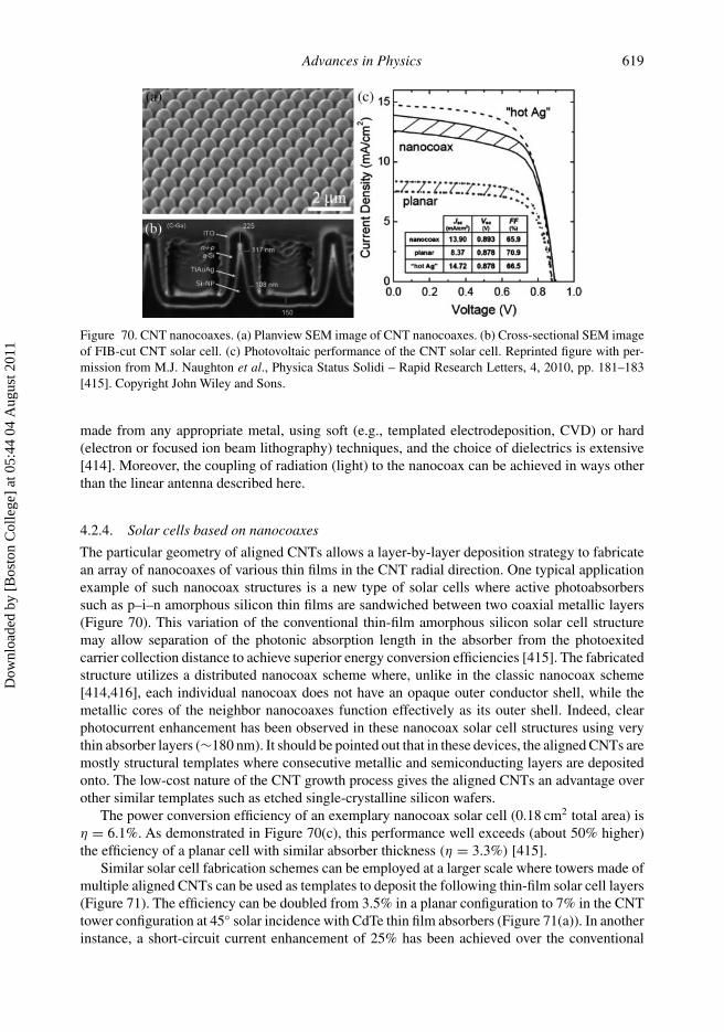
Advances in Physics 619
Figure 70. CNT nanocoaxes. (a) Planview SEM image of CNT nanocoaxes. (b) Cross-sectional SEM imageof FIB-cut CNT solar cell. (c) Photovoltaic performance of the CNT solar cell. Reprinted figure with per-mission from M.J. Naughton et al., Physica Status Solidi – Rapid Research Letters, 4, 2010, pp. 181–183[415]. Copyright John Wiley and Sons.
made from any appropriate metal, using soft (e.g., templated electrodeposition, CVD) or hard(electron or focused ion beam lithography) techniques, and the choice of dielectrics is extensive[414]. Moreover, the coupling of radiation (light) to the nanocoax can be achieved in ways otherthan the linear antenna described here.
4.2.4. Solar cells based on nanocoaxes
The particular geometry of aligned CNTs allows a layer-by-layer deposition strategy to fabricatean array of nanocoaxes of various thin films in the CNT radial direction. One typical applicationexample of such nanocoax structures is a new type of solar cells where active photoabsorberssuch as p–i–n amorphous silicon thin films are sandwiched between two coaxial metallic layers(Figure 70). This variation of the conventional thin-film amorphous silicon solar cell structuremay allow separation of the photonic absorption length in the absorber from the photoexitedcarrier collection distance to achieve superior energy conversion efficiencies [415]. The fabricatedstructure utilizes a distributed nanocoax scheme where, unlike in the classic nanocoax scheme[414,416], each individual nanocoax does not have an opaque outer conductor shell, while themetallic cores of the neighbor nanocoaxes function effectively as its outer shell. Indeed, clearphotocurrent enhancement has been observed in these nanocoax solar cell structures using verythin absorber layers (∼180 nm). It should be pointed out that in these devices, the aligned CNTs aremostly structural templates where consecutive metallic and semiconducting layers are depositedonto. The low-cost nature of the CNT growth process gives the aligned CNTs an advantage overother similar templates such as etched single-crystalline silicon wafers.
The power conversion efficiency of an exemplary nanocoax solar cell (0.18 cm2 total area) isη = 6.1%. As demonstrated in Figure 70(c), this performance well exceeds (about 50% higher)the efficiency of a planar cell with similar absorber thickness (η = 3.3%) [415].
Similar solar cell fabrication schemes can be employed at a larger scale where towers made ofmultiple aligned CNTs can be used as templates to deposit the following thin-film solar cell layers(Figure 71). The efficiency can be doubled from 3.5% in a planar configuration to 7% in the CNTtower configuration at 45◦ solar incidence with CdTe thin film absorbers (Figure 71(a)). In anotherinstance, a short-circuit current enhancement of 25% has been achieved over the conventional
Dow
nloa
ded
by [
Bos
ton
Col
lege
] at
05:
44 0
4 A
ugus
t 201
1

620 Y. Lan et al.
Figure 71. (a) CdTe solar cell deposited on towers of aligned CNT arrays; inset: SEM image of a cut tower. (b)SEM image of line-patterned array of coaxial MWCNTs (ITO and amorphous silicon-coated CNTs). Inset:schematic of the coaxial MWCNTs. Scale bar: 2 micron. (a) Reprinted from JOM – Journal of the Minerals,Metals and Materials Society, 59 pp. 39–42, R. Camacho et al. [417]. Copyright (2001) from Springer. (b)Reprinted figure with permission from H. Zhou et al., Advanced Materials, 21, 2009, pp. 3919–3923 [418].Copyright John Wiley and Sons.
planar structure, owing to the highly effective light-trapping structure of the coaxial MWCNT/a-Si:H nanowire array (Figure 71(b)) [418]. In this case, the nanocoax effect is absent due to thelarge dimensions of the structures and the performance enhancement is purely expected from theenlarged surface area of the absorber material and the higher ray scattering frequency for broadincident angles due to the 3D geometry.
4.3. Nanoelectrode-based sensors
Individual CNTs can be semiconducting or metallic, and are good candidates for electrode mate-rials. So CNT arrays have been fabricated into nanoelectrode arrays for various applications. Inthis section, we review the CNT nanoelectrode arrays and their applications.
4.3.1. Nanoelectrode arrays
Microelectrode arrays consisting of hundreds of metal microelectrodes with diameters of severalmicrometers have been fabricated by lithographic techniques [419]. The microelectrodes showmany advantages over the conventional macroelectrodes such as high mass sensitivities, enhancedmass transport, and a decreased influence from the solution resistance. Further size reductions ofeach individual electrode to nanometers and an increase in the density of electrodes can improve thedetection limits and the signal-to-noise ratio [170] since the noise level depends on the active areaof the individual electrode, whereas the signal strength depends on the total area of the electrodes[420]. Such 2D nanoelectrode arrays have been fabricated based on gold nanowires [421].
SWCNTs exhibit high electrical conductivities and are the most promising candidates forminiaturizing electrodes beyond the micrometer-scale currently used in electronics. Up to now,CNT-based nanoelectrodes have already been fabricated [422–431].
CNT nanoelectrode arrays are fabricated with aligned CNTs of low site densities. Such alignedCNTs can be grown by PECVD method from catalytic patterns, as described in Section 2.1.3.2.To make each CNT working as an individual nanoelectrode, the spacing needs to be sufficientlylarger than the CNT diameters to prevent the diffusion layer from overlapping with the neighbor-ing electrodes [432,433]. Based on these low-site-density CNTs, nanoelectrode arrays consist ofmillions of nanoelectrodes (with each electrode being less than 100 nm in diameter). Because thetotal current of the loosely packed electrode arrays is proportional to the total number of individual
Dow
nloa
ded
by [
Bos
ton
Col
lege
] at
05:
44 0
4 A
ugus
t 201
1

Advances in Physics 621
Figure 72. Fabrication scheme of the nanoelectrode arrays. (a) Ni nanoparticle electrodeposition. (b) Growthof aligned CNT. (c) Coating of SiO2 and M-bond. (d) Polishing to expose CNTs. Reprinted with permissionfrom Y. Tu et al., Nano Letters, 3, 2003, pp. 107–109 [170]. Copyright (2003) American Chemical Society.
electrodes, the number of electrodes totaling in the millions is highly desirable. The size reduc-tion of each individual CNT electrode and the increased total number of CNT electrodes resultin improvements in both the signal-to-noise ratio and the detection limits of CNT array-basednanoelectrode arrays [420,421].
The fabrication of CNT nanoelectrode arrays has been described in existing literatures [170,178,434]. Figure 72 shows the SiO2/epoxy-coated nanoelectrode arrays. The CNTs are directlygrown on the conductive substrate to ensure good electrical conductivity to the external circuit. Ina typical experiment, Ni catalytic nanoparticles are electrodeposited on a Cr-coated Si substrateof 1 cm2 in area (Figure 72(a)). The site density of the catalytic nanoparticles is low. Aligned CNTarrays are then grown from those Ni nanoparticles by PECVD (Figure 72(b)). Next, the CNTspacings are filled by epoxy spin-coating or various other coating methods (Figure 72(c)). In atypical filling process, an epoxy-based polymer with a curing agent is spin-coated on the substrateand covers up to half of the CNT length. The protruding parts of the CNTs are mechanicallyremoved subsequently by polishing (Figure 72(d)).
Figure 73 shows the SEM images of the CNT nanoelectrode array fabrication steps correspond-ing to the scheme shown in Figure 72. The bright dots in Figure 72(a) are the electrodepositedNi nanoparticles that are randomly distributed on the substrate. Figure 72(b) shows the low den-sity aligned CNT array grown by PECVD from the Ni nanoparticles. Figure 72(c) shows themorphology after coating with a thin layer of SiO2 followed by a second layer of epoxy film. The
Dow
nloa
ded
by [
Bos
ton
Col
lege
] at
05:
44 0
4 A
ugus
t 201
1
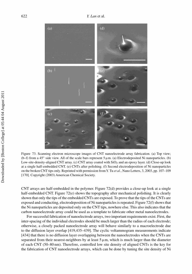
622 Y. Lan et al.
Figure 73. Scanning electron microscope images of CNT nanoelectrode array fabrication. (a) Top view;(b–f) from a 45◦ side view. All of the scale bars represent 5 μm. (a) Electrodeposited Ni nanoparticles. (b)Low-site-density-aligned CNT array. (c) CNT array coated with SiO2 and an epoxy layer. (d) Close-up lookat a single half-embedded CNT. (e) CNTs after polishing. (f) Second electrodeposition of Ni nanoparticleson the broken CNT tips only. Reprinted with permission fromY. Tu et al., Nano Letters, 3, 2003, pp. 107–109[170]. Copyright (2003) American Chemical Society.
CNT arrays are half-embedded in the polymer. Figure 72(d) provides a close-up look at a singlehalf-embedded CNT. Figure 72(e) shows the topography after mechanical polishing. It is clearlyshown that only the tips of the embedded CNTs are exposed. To prove that the tips of the CNTs areexposed and conducting, electrodeposition of Ni nanoparticles is repeated. Figure 72(f) shows thatthe Ni nanoparticles are deposited only on the CNT tips, nowhere else. This also indicates that thecarbon nanoelectrode array could be used as a template to fabricate other metal nanoelectrodes.
For successful fabrication of nanoelectrode arrays, two important requirements exist. First, theinter-spacing of the individual electrodes should be much larger than the radius of each electrode;otherwise, a closely packed nanoelectrode array will behave similarly to a macroelectrode dueto the diffusion layer overlap [419,435–439]. The cyclic voltammogram measurements indicate[434] that there is no diffusion layer overlapping between the nanoelectrodes when the CNTs areseparated from their nearest-neighbors by at least 5 μm, which is much larger than the diameterof each CNT (50–80 nm). Therefore, controlled low site density of aligned CNTs is the key forthe fabrication of CNT nanoelectrode arrays, which can be done by tuning the site density of Ni
Dow
nloa
ded
by [
Bos
ton
Col
lege
] at
05:
44 0
4 A
ugus
t 201
1

Advances in Physics 623
Figure 74. Cyclic voltammetry curve of the carbon nanoelectrode arrays. The curve was taken in a solutionof 4 mM K3Fe(CN)6 in 0.5 M KNO3. The scan rate was 40 mV/s. Reprinted with permission from Y. Tuet al., Nano Letters, 3, 2003, pp. 107–109 [170]. Copyright (2003) American Chemical Society.
nanoparticle catalysts, using an electrochemical deposition method [178]. Secondly, there mustbe a passivation layer that can protect the underlying conducting layer as well as prevent currentleakage and corrosion. Both inorganic materials, such as SiO2 and Si3N4, and organic materials,such as epoxy and photo resist, have been previously tested [440]. The ideal passivation layer iscaptive and crack-free, long lasting in aqueous electrolyte solutions, adhering well to substratesand electrodes, mechanically strong, and easily processable. Insulating materials should be goodenough to prevent the current leakage that results in the distortion of the cyclic voltammetrycurve. Very low background current and leakage current are achieved when the CNT arrays areexcellently sealed by the spin-coated epoxy resin, which enables the sensitivity analysis [434].
The cyclic voltammetry curve of the CNT nanoelectrode arrays (Figure 74) indicates that thesignal (in the range of microamperes) generated from the nanoelectrode arrays is much largercompared to the signal (a few picoamperes) generated from a couple of carbon electrodes witha similar disk shape [441] because the total current for the loosely packed electrode array isproportional to the number of individual electrodes [433].
To date, many research groups have fabricated CNT nanoelectrode arrays [170,429,435,441].These are based on the advantages of CNT materials over conventional macroelectrodes such asenhanced mass transport and decreased influence from the solution resistance, which makes anexcellent electrochemical transducer in various applications. The aligned CNT nanoelectrode hasa high mass sensitivity, an increased mass-transport rate, a decreased influence from the solutionresistance, and a higher signal-to-noise ratio, leading to a much lower background current thanother electrode configurations. For example, the CNT array of nanoelectrodes can produce amuch higher current than a single nanoelectrode [442] and bundles of CNTs [443,444], which canimprove the signal-to-noise ratio.
The nanoelectrodes have many practical applications such as ultrasensitive electrochemicalsensors for chemical and biological sensing. Below we will review some of these applications.
4.3.2. Ion sensors
The unique electronic, chemical, and mechanical properties of CNTs make them extremely attrac-tive for applications in chemical and biochemical sensors [318,445]. Most CNT sensing platforms
Dow
nloa
ded
by [
Bos
ton
Col
lege
] at
05:
44 0
4 A
ugus
t 201
1

624 Y. Lan et al.
take advantage of the unique properties of CNTs, such as increased electrode surface areas [446]and high electron transfer rates [447]. It is well known that the electron transfer rate of the electrodeis dominated by its surface structure. The sidewall atomic structure of MWCNTs is similar to thegraphitic basal plane and the open-end of CNTs is similar to the edge-plane. Because the electrontransfer on edge-plane graphite is faster than that on the basal-plane graphite, the open ends ofthe CNTs have higher electron transfer rates similar to a graphitic edge-plane electrode [448],while the sidewalls exhibit very low electron transfer rates similar to the graphitic basal plane.It is reported that the high-site-density CNT array and CNT forest show fast electron transfercharacteristics [447,449].
The CNT forest electrodes or high-site-density CNT arrays do not act as individual nanoelec-trodes because the high site density of the CNTs causes the overlapping of diffusion layers ofindividual nanoelectrodes, as discussed in Section 4.1.1. So the low-site-density CNT arrays areemployed as CNT ion-sensing platforms. To make each CNT work as an individual nano-electrode,the spacing needs to be sufficiently larger than the CNT diameter to prevent diffusion layer fromoverlapping with the neighboring electrodes. The microsphere lithography method is a good tech-nique to prepare nanoparticle catalysts with low site densities. The electrodeposition method isalso suitable to prepare such catalysts for low-site-density growth. In order to take advantage of ahigh electron transfer rate, the CNT tips are always opened. To eliminate the background currentleakage generated from the sidewalls of CNTs and the electrode capacitance, the sidewalls aresealed with an epoxy passivation layer. Such a structure provides a high signal-to-noise ratio.
The CNT sensoring platforms are fabricated similarly to nanoelectrode arrays, as shown inFigure 72. In a typical process, a CNT array is grown first by PECVD [429]. The site density of thealigned CNTs is controlled by tuning the site density of catalytic nanoparticles. The site densityis typically 1–3 × 106 cm−2, depending on the final length of CNTs. An epoxy resin layer ofmicrons thick is coated on the aligned CNT arrays grown on the substrate surface using a standardspin-coating method. The aligned CNTs show very good mechanical stabilities and preserve theirvertical alignment. The CNTs are half-embedded in the resin with 2–3 μm of length protrudingfrom the resin surface. By using a lens paper to gently polish the coated CNTs, the protrudingparts are broken and removed by ultrasonication in water. Then an electrical connection is madeto the CNT substrate to produce an ion-sensing platform.
Square-wave voltammetric measurements are carried out in an electrochemical cell containinga CNT-array working electrode, a Ag/AgCl reference electrode, and a platinum wire counter-electrode. A magnetic stirrer together with a magnetic bar provides the convectional conditionswhen needed.
Compared to the traditional macroelectrode, the aligned CNT nanoelectrode has a high masssensitivity, an increased mass-transport rate, a decreased influence from the solution resistance,and a higher signal-to-noise ratio, leading to a much lower background current. The CNT arraysensing platform shows potential to detect very low concentrations of heavy metal ions comparedto a traditional bulk and macro-electrode sensing platform [450].
Figure 75(a) presents a typical square voltammogram for a mixture containing 5 μg/l cadmiumand lead ions. A well-defined, undistorted, sharp signal with a favorable resolution is obtained.The peak potentials of cadmium and lead are −0.75 and −0.55V, respectively. The strippingsignal for the selected target metals is surrounded with low background contributions, indicatingeffective sealing on the sidewalls of CNTs during the preparation of the nanoelectrode array. Thevery attractive signal-to-noise characteristics and peak resolution indicate that the aligned CNTarray can be used as an excellent electrochemical sensing platform [450].
Figure 75(b) displays the square voltammogramic response of an aligned CNT array for increas-ing cadmium ion concentrations under the optimum experimental conditions. Well-defined peaks,proportional to the concentration of the corresponding cadmium, are observed.A linear relationship
Dow
nloa
ded
by [
Bos
ton
Col
lege
] at
05:
44 0
4 A
ugus
t 201
1

Advances in Physics 625
Figure 75. (a) Typical square wave voltammogram of 5 μg/l cadmium and lead in 0.1 M acetate buffer (pH4.5) in the presence of 500 μg/l bismuth. (b) Square wave voltammogramic response of cadmium solutionwith increasing concentration (0.5, 1, 2, 4, 6, 8 μg/l). The small shoulder peaks at −0.57V are attributedto a trace of lead in the blank solution. A square-wave voltammetric scan with step potential: 5 mV; ampli-tude: 20 mV; and frequency: 25 Hz. G Liu et al., Analyst 130, pp. 1098–1101, 2005 [450] – Reproduced bypermission of The Royal Society of Chemistry.
between the stripping current and cadmium concentration is obtained covering the concentrationrange from 0.5 to 8 μg/l, as the linear regression equation being I(nA) = 37.054 × concentration(μg/l)–10.486, with a correlation coefficient of 0.9955. The detection limit is improved signifi-cantly by increasing the accumulation time. A detection limit of 0.04 μg/l (40 ppm) is estimatedon the basis of an S/N = 3 characteristic of the 0.1 μg/l data points in connection with a 240-saccumulation time. Such improvement of the stripping signal and extremely low detection limitbenefit from the high signal-to-noise ratio of CNT arrays.
Lead is regarded as a highly toxic metal ion to a wide variety of organs in both human andanimals, including nerves, immune, reproductive, and gastrointestinal systems. The ability torapidly detect a trace amount of Pb2+ species on-site is very desirable. Figure 76 shows that thevoltammetric response is a linear function of Pb2+ concentrations ranging from 2 to 100 ppb [429].The lead concentration can be detected at a very low level. The inset shows the response peaks of2 to 100 ppb of Pb2+.
4.3.3. Gas sensors
A chemical sensor can be defined as a device that responds to changes in the local chemical envi-ronment. The response should be predictable such that it scales with the magnitude of change in
Dow
nloa
ded
by [
Bos
ton
Col
lege
] at
05:
44 0
4 A
ugus
t 201
1

626 Y. Lan et al.
Figure 76. The voltammetric response (current) of Pb2+ in 0.1 M NaNO3 solution as a function of Pb2+concentration, measured after 3 min of deposition. Pulse amplitude: 25 mV; step amplitude: 5 mV; frequency:100 Hz. The voltammograms correspond to Pb2+ concentration of 2, 5, 25, 50, and 100 ppb. Reprinted figurewith permission from Y. Tu et al., Electroanalysis, 17, 2005, pp. 79–84 [429]. Copyright John Wiley andSons.
the environment. Additionally, a chemical sensor should be sensitive and selective to the chemicalmolecule concerned. CNTs are good candidates for chemical detection, because the nanoscaledimensions and exceptionally large surface area of CNTs make them more environmentally sen-sitive than bulk carbon materials. To date, CNTs have shown sensitivities toward gases such asNH3, NO2, H2, C2H4, CO, SO2, H2S, and O2, and most of these demonstrated sensors are fabri-cated from random or individual CNTs in the configurations of CNT-based field-effect transistors[303,308,451,452]. The aligned CNTs can be 1D ordered, directly grown on random catalysts byPECVD method (see Section 2.1.3.1) or by thermal CVD method (see Section 2.1.1), or be 3Dordered, grown from 2D ordered catalysts by PECVD method (see Section 2.1.3.2).
There are two kinds of CNT array gas sensors. One is the two-terminal gas sensor (Figure 77(a))and the other is three-terminal, as shown in Figure 77(b). The two-terminal sensors are simple,
Figure 77. Schematic cross-section views of (a) two-terminal and (b) three-terminal CNT gas sensors. (a)Reprinted from Sensors and Actuators B: Chemical, 93, Y.M. Wong et al., pp. 327–332. Copyright (2003),with permission from Elsevier. (b) Reprinted from Diamond and Related Materials, 14, C.S. Huang et al.,pp. 1872–1875. Copyright (2005), with permission from Elsevier.
Dow
nloa
ded
by [
Bos
ton
Col
lege
] at
05:
44 0
4 A
ugus
t 201
1

Advances in Physics 627
while the sensitivity of the three-terminal sensors is higher. Let us review these gas sensors asfollows.
CNT-based gas sensors were demonstrated as early as in 2000 when the responses of CNTfield-effect transistor, mainly made of a single semiconducting SWCNT, to NO2 and NH3 gaseswere reported [303]. NH3 exposure resulted in a shift in the transfer characteristic gate voltageof approximately -4V, while NO2 exposure created a shift of approximately +4V. Alternatively,when the transistor was held at a constant gate voltage of VG = 0V, exposure to NH3 resulted ina decrease in the device current, while NO2 exposure (VG = +4V) resulted in an increase. Theresponse time to 200 ppm NO2 was a few seconds, and the sensitivity, defined as the resistanceafter exposure divided by the initial resistance, was approximately 100–1000. The response timeto approximately 1% NH3 was a few minutes with a sensitivity between 10 and 100. A floodgateof interests in the development of CNT-based gas sensors was generated by these initial resultsof CNT gas-sensing capabilities. Up to now, more than 1000 reports focused specifically on theapplication of CNTs in gas sensors have been published [455]. The gas and vapor sensors madeof individual CNTs or CNT networks are well reviewed recently [455–461]. Some CNT arraysensors are also reviewed recently [459]. Here we focus on the application of CNT arrays in gasand vapor sensors.
CNT array gas sensors have an outstanding sensitivity at low temperatures of fast responseand high selectivity [462]. Several types of gas sensors using CNTs have been proposed. Oneis the gas ionization sensor, in which CNTs are used as field-emission electrodes to ionize theanalyzing gas, resulting in high gas selectivity and sensitivity [463]. Another type is based on achange of the electrical conductance of CNTs when adsorbing gas molecules. The mechanismof the CNT gas sensors is based on the dependence of CNT electrical resistance with ambientgas concentration. When the p-type semiconducting CNTs adsorb oxidizing molecules, electricalresistance of the CNTs decreases with the number increase of the adsorbed gas molecules. In otherwords, the electrical conductance of p-type semiconducting CNTs is modified by the electrontransfer between CNTs and oxidizing or reducing gas molecules adsorbed on the CNT surfaces.The second type of gas sensors has extremely high sensitivity and fast response at room temperatureand is compatible with integrated circuit fabrication.
4.3.3.1 Hydrogen gas sensors The risk of explosion is the primary reason for the needs toaccurately measure H2 levels since concentrations as low as 4% in air can become explosive. BareCNTs do not show appreciable sensitivity to H2 due to the weak binding energy of hydrogen to thesurfaces of CNTs [464]. After being decorated or functionalized by Pd or Pt nanoparticles on theirsidewalls, the CNTs can detect the ppm level of H2 gas [465,466]. It is believed that H2 dissociatesinto atomic hydrogen on the Pd or Pt nanoparticle surface at room temperature to form PdH2 orPtH2, decreasing the Pd or Pt work function and leading to electron donation into the CNTs fromthe nanoparticles [467,468]. As a result, the electrical conductance of the Pd-decorated SWCNTdecreases, yielding a response time of a few seconds.
Figure 78(a) shows an SEM image of a vertically aligned CNT array grown in an AAO(anodized aluminum oxide) template used for room-temperature detection of ppm concentra-tions of H2. The CNTs are coated with a Pd film to form a two-terminal gas sensor to enhancethe sensitivity of the H2 detection. The electrical resistance varies with the concentration of H2
(Figure 78(b)). The Pd-coated CNT array sensor is sensitive to hydrogen gas concentrations from100 ppm to 1.5% at room temperature.
H2 is also detected by a Pd/MWCNTs/n-Si thin-film sandwich structure [453]. The thin layerof Pd is sputtered on top of the MWCNT array. The current is reduced in the presence of hydrogenand the reduction is attributed to an increase in the barrier height between the Pd-CNT interfaceafter H2 adsorption.
Dow
nloa
ded
by [
Bos
ton
Col
lege
] at
05:
44 0
4 A
ugus
t 201
1
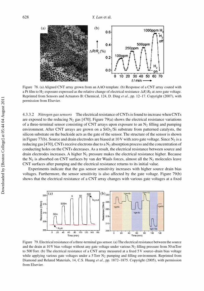
628 Y. Lan et al.
Figure 78. (a) Aligned CNT array grown from an AAO template. (b) Response of a CNT array coated witha Pt film to H2 exposure expressed as the relative change of electrical resistance R/R0 at zero gate voltage.Reprinted from Sensors and Actuators B: Chemical, 124, D. Ding et al., pp. 12–17. Copyright (2007), withpermission from Elsevier.
4.3.3.2 Nitrogen gas sensors The electrical resistance of CNTs is found to increase when CNTsare exposed to the reducing N2 gas [470]. Figure 79(a) shows the electrical resistance variationsof a three-terminal sensor consisting of CNT arrays upon exposure to an N2 filling and pumpingenvironment. After CNT arrays are grown on a SiO2/Si substrate from patterned catalysts, thesilicon substrate on the backside acts as the gate of the sensor. The structure of the sensor is shownin Figure 77(b). Source and drain electrodes are biased at 10V with zero gate voltage. Since N2 is areducing gas [470], CNTs receive electrons due to a N2 absorption process and the concentration ofconducting holes on the CNTs decreases. As a result, the electrical resistance between source anddrain electrodes increases. A higher N2 pressure makes the electrical resistance higher. Becausethe N2 is absorbed on CNT surfaces by van der Waals forces, almost all the N2 molecules leaveCNT surfaces after pumping and the electrical resistance returns to its initial value.
Experiments indicate that the gas sensor sensitivity increases with higher source drain biasvoltages. Furthermore, the sensor sensitivity is also affected by the gate voltage. Figure 79(b)shows that the electrical resistance of a CNT array changes with various gate voltages at a fixed
Figure 79. Electrical resistance of a three-terminal gas sensor. (a) The electrical resistance between the sourceand the drain at 10V bias voltage without any gate voltage under various N2 filling pressure from 50 mTorrto 500 Torr. (b) The electrical resistance of a CNT array measured at a fixed 5V source–drain bias voltagewhile applying various gate voltages under a 5 Torr N2 pumping and filling environment. Reprinted fromDiamond and Related Materials, 14, C.S. Huang et al., pp. 1872–1875. Copyright (2005), with permissionfrom Elsevier.
Dow
nloa
ded
by [
Bos
ton
Col
lege
] at
05:
44 0
4 A
ugus
t 201
1

Advances in Physics 629
5V source–drain voltage in a 5 Torr N2 pumping and filling environment. The initial electricalresistance increases when a positive gate voltage is applied and decreases with a negative gatevoltage. The resistance of CNT array restores its initial value after a cycle of N2 filling andpumping under different positive and negative gate voltages. The sensor sensitivity increases withthe decrease in the gate voltage from positive to negative due to the increase in the gas-bindingsites caused by a negative gate voltage.
4.3.3.3 Nitrous oxide gas sensors Nitrous oxides such as nitrogen monoxide (NO) and nitrogendioxide (NO2) are typical air pollutants that cause environmental problems. There are demandsfor small and cheap gas sensors for NO detection in medical applications and scientific research.
Figure 80 shows a two-terminal gas sensor with interdigitated electrodes. The platinum inter-digitated electrodes are deposited on the CNT arrays to provide larger sensing areas and sufficientcontact areas between the electrodes and the coated CNTs. The resistance change of CNTs undergas exposure is detected by two-terminal resistors with a DC voltage. NO2 exposure drasticallydecreases the electrical resistance of the CNT arrays and completely removing the gas exposurerestores the initial resistance of CNT arrays. The conductance change of the sensors shows alinear response to the gas concentration upon exposure to NO2, no matter MWCNT arrays [471]or SWCNT arrays [435] are used.
Besides NO2, NO can also be detected using gas sensors with identical structures [471,472].
4.3.3.4 Ammonia gas sensors In the case of chemical gas sensors based on electrical resistance,it is difficult to detect gas molecules with low adsorption energy. Compared to these resistance-based gas sensors, ionization gas sensors based on the finger-printing ionization characteristics ofthe detected gases can identify different kinds of gas molecules when the detected gas moleculesare ionized. There are no limits to identify gases with low adsorption energy and poor chargetransfer with the sensing materials. Detection of inert gases or gas mixtures can be easily achievedin an ionization chamber. Therefore, the effect of gas adsorption on CNT field-emission propertiesand CNT-enhanced ionization gas sensors has attracted a great amount of research interests.
Figure 81 shows a diagram of an ionization gas sensor with an aligned MWCNT array as theanode. It consists of an MWCNT array anode, an Al plate cathode, and a 150 μm thick glassinsulator between them (Figure 81(a)). Under electric fields, individual MWCNTs create very
Figure 80. Two-terminal NO2 gas sensor. (a) Schematic diagram of CNTs patterned with platinum contacts.(b) Electrical resistance variation of CNT arrays at an operating temperature of 165◦C and NO2 concentra-tion between 10 and 100 ppb. (a) Reprinted from Diamond and Related Materials, 17, T. Ueda et al., pp.1586–1589. Copyright (2008), with permission from Elsevier. (b) Reprinted from Diamond and RelatedMaterials, 13, L. Valentini et al., pp. 1301–1305. Copyright (2004), with permission from Elsevier.
Dow
nloa
ded
by [
Bos
ton
Col
lege
] at
05:
44 0
4 A
ugus
t 201
1

630 Y. Lan et al.
Figure 81. Ionization gas sensors. (a) Schematic diagram of the CNT array ionization gas sensor device. (b)SEM micrograph of vertically aligned MWCNT arrays used as the anode. Reprinted by permission fromMacmillan Publishers Ltd: Nature [463], copyright (2003).
Figure 82. Electrical properties of ionization gas sensors. (a) Breakdown voltage as a function of gas con-centration. The breakdown voltage varies only slightly with gas concentration. (b) Discharge current atbreakdown voltage as a function of gas concentration. The discharge current varies logarithmically withconcentration. Reprinted by permission from Macmillan Publishers Ltd: Nature [463], copyright (2003).
high nonlinear electric fields near the CNT tips, resulting in the formation of highly ionized gasesthat surrounds the MWCNT tips and the formation of a self-sustaining interelectrode discharge atvery low voltages.
The precise breakdown voltage provides a finger-print to each gas and indicates the potentialfor gas identification within a mixture of gases. The breakdown voltage is rarely affected bythe concentration in the range of 10−5–10−1 mol/l, while the breakdown voltage of each gas isunique (Figure 82(a)). Therefore by monitoring the breakdown voltage of the gas, its identity can bedetermined. The discharge current of each gas increases logarithmically with the gas concentration.Therefore, the discharge current provides a convenient means to quantify the concentration of thegas being detected (Figure 82(b)).
The ionization sensor works in the concentration range of 10−5–10−1 mol/l. In the lowerconcentration, the breakdown voltage decreases with air or the argon pressure below 10−5 mol/l
Dow
nloa
ded
by [
Bos
ton
Col
lege
] at
05:
44 0
4 A
ugus
t 201
1

Advances in Physics 631
[473,474] and varies slightly with the pressure above 10−5 mol/l [473]. Besides ammonia, argonand helium gases can also be detected using the ionization gas sensors.
NH3 is also measured from the electrical resistance variation of CNT arrays using two-terminalCNT sensors [472,475]. NH3 exposure increases the electrical resistance of p-type CNT arrays.
4.3.3.5 Other gas sensors Besides the exposure of the above gases, H2O, C2H6, and ethanolexposures also increase the electrical resistance of a CNT array and can be determined by two-terminal sensors [472].After being coated with conducting polymers such as polyvinyl acetate, thevertically aligned CNT arrays can also be used to detect cyclohexane and ethanol from electricalresistance variations [476].
4.3.4. Biosensors
CNTs can be functionalized with different biomolecules such as DNA and protein [444,448,477,478]. It was found that the electronic transport and thermopower of CNTs are very sensitive tosubstances that affect the amount of injected charge [22,303]. Based on these unique propertiesincluding the high electron transfer rate [448] and the high electrocatalytic activity [479,480], sev-eral research groups have demonstrated that bundles of CNTs [443,444], CNT membranes [481],polymer–CNT composites [434,479,482,483], and CNT-modified electrodes [445,478,484] canbe used as effective electrochemical biosensors. The main advantages of CNTs are the nano-size of the CNT-sensing element and the corresponding small amount of materials required fordetectable response. The well-aligned CNT arrays have been employed to work as ribonucleicacid (RNA) sensors [431], enzymes sensors [449], DNA sensors, and even protein sensors. Thebiological applications of aligned CNT arrays are reviewed recently [485–487]. Here we focus onthe structure properties of these CNT array biosensors and their working mechanisms.
4.3.4.1 Glucose sensors Because of the high demand for blood glucose monitoring, significantresearch and development efforts have been devoted to producing reliable glucose sensors for invitro or in vivo applications. The measurement principle of oxidase-based amperometric biosensorspreviously relied on the immobilization of oxidase enzymes on the surface of various electrodesand the detection of the current associated with the redox product in the biological reaction.To increase the selectivity and sensitivity of amperometric biosensors, artificial mediators andpermselective coatings are often used in the biosensor fabrication. Artificial mediators are used toshuttle electrons between the enzyme and the electrode to allow operation at low potentials. Thisapproach can minimize interferences with coexisting electro-active species, but the stability andthe toxicity of some mediators limit their in vivo applications. Permselective membranes are alsoused to eliminate interferences.
A mediator- and membrane-free biosensor was invented using CNT arrays [434]. The inno-vative method provides a means for measuring the cathodic current of enzymatically liberatedhydrogen peroxide in metal-dispersed carbon paste biosensors. The idea of the mediator- andmembrane-free biosensor is based on the reduction of hydrogen peroxide [488,489], the strongelectrocatalytic effect, and a high electron-transfer rate of CNTs [436]. The technique provided anew approach for biosensor development [488,489].
The glucose sensors are also based on the CNT nanoelectrode arrays with low site densities. Thealigned CNT arrays are first fabricated as the starting building block (Figure 83(a)). The detailedfabrication procedure of the CNT nanoelectrode arrays is described in Section 4.3.1. The CNTnanoelectrode arrays are pre-treated for functionalization in 1.0 M NaOH at 1.5V for 90 s. Afterthe electrochemical treatment, some functional groups (e.g., carboxylic acid) are created at theCNT tips (Figure 83(b)). Then enzymes are attached to the broken tips of the polished CNT arrays
Dow
nloa
ded
by [
Bos
ton
Col
lege
] at
05:
44 0
4 A
ugus
t 201
1

632 Y. Lan et al.
Figure 83. Fabrication of a glucose biosensor based on CNT nanoelectrode arrays. (a) CNT nanoelectrodearray with exposed CNT tips. (b) Electrochemical treatment of the CNT nanoelectrode arrays for function-alization. (c) Coupling of the enzyme (GOx) to the functionalized CNT nanoelectrode arrays. Reprintedwith permission from Y. Lin et al., Nano Letters, 4, 2004, pp. 191–195 [434]. Copyright (2004) AmericanChemical Society.
using standard water-soluble coupling agents 1-ethyl-3-(3-dimethylaminopropyl) carbodiimide(EDC) and N-hydroxy-sulfo-succinimide (sulfo-NHS) by forming amide linkages between theiramine residues and carboxylic acid groups on the CNT tips [434,436] (Figure 83(c)). In a typicalprocedure, the activated CNT nanoelectrode arrays are then immersed in a freshly prepared 10 mlaqueous solution of EDC (10 mg/ml). With stirring, 300 mg of sulfo-NHS is added to the solution.The pH of the solution is adjusted to 7. The reaction is allowed to occur at room temperature for2 h. Then the nanoelectrode is washed quickly with cold water and immediately immersed into adegassed solution (10 ml) with the desired amount of glucose oxidase (GOx) (2 mg/ml) in a 0.1 Mphosphate buffer solution (pH 7.4) with stirring. The resultant nanoelectrode array biosensor isstored at 4◦C before use.
The amperometric experiment was performed in a standard single-compartment electrochem-ical cell that contained a nanoelectrode array electrode, a Ag/AgCl reference electrode, and aplatinum wire auxiliary electrode. The electrochemical detector is connected to a portable com-puter. The amperometric response of the glucose biosensor based on CNT nanoelectrode arraysto glucose was recorded under steady-state conditions in a 0.1 M phosphate buffer (pH 7.4) byapplying a desired potential (for interference experiments, +0.4 and −0.2V; for the calibrationexperiment, −0.2V) to the biosensor. The background response of the biosensor is allowed todecay to a steady state with stirring. When the background current becomes stable, a solution ofglucose is injected into the electrolytic cell, and its response is measured and recorded.
The amperometric responses at the nanoelectrode array glucose biosensors for each successiveaddition of 2 × 10⁻³ M glucose are presented in Figure 84. The inset is the calibration curve. Well-defined current responses for glucose were obtained by the nanoelectrode array biosensor. Thereaction occurring at the biosensor is very fast in reaching a dynamic equilibrium upon each
Dow
nloa
ded
by [
Bos
ton
Col
lege
] at
05:
44 0
4 A
ugus
t 201
1

Advances in Physics 633
Figure 84.Amperometric responses of a CNT nanoelectrode array biosensor to successive additions of 2 mMglucose. Reprinted with permission from Y. Lin et al., Nano Letters, 4, 2004, pp. 191–195 [434]. Copyright(2004) American Chemical Society.
addition of the sample solution, generating a steady-state current signal within 20–30 s. The linearresponse of the glucose biosensor to glucose is up to about 30 mM of glucose, which is higherthan the 15 mM required for practical uses in the detection of blood glucose. The signal responsecurve is effective at low detection limits for glucose because of favorable signal-to-noise ratiocharacteristics at −0.2V. The limit of detection, based on a signal-to-noise ratio of 3, is 0.08 mM.
Besides the detection of glucose, such CNT nanoelectrode biosensors can also be used to detectascorbic acid, uric acid, and acetaminophen. The selectivity advantage accrued from the hydro-dynamic voltammograms is demonstrated in Figure 85 which compares amperometric responsesfor relevant physiological levels of glucose, ascorbic acid, acetaminophen, and uric acid at theGOx-modified nanoelectrode array at potentials of +0.4 and −0.2V, respectively. Amperometricresponses are obtained by a batch addition of interfering species (0.5 mM ascorbic acid, 0.5 mMuric acid, and 0.5 mM acetaminophen) after the 5 mM glucose addition at two different poten-tials (+0.40 and −0.2V). Well-defined cathodic and anodic glucose responses are obtained bythe nanoelectrode array biosensor at potentials of +0.4 and −0.2V. At an operating potential of+0.40V, the glucose response is overlapped by large anodic contributions from ascorbic acid,uric acid, and acetaminophen. The use of a lower operating potential greatly reduces these con-tributions. No interference is observed at a potential of −0.20V for the interference species,indicating high selectivity toward the glucose substrate. Such a highly selective response to glucoseis obtained by the nanoelectrode array biosensor without the use of mediators and permselectivemembranes [434].
Cyclic voltammetric experiments indicate that the oxidation of the interfering species at thenanoelectrode array starts at about +0.20V (ascorbic acid) and +0.30V (acetaminophen, uricacid) with no reduction until −0.2V [434].
4.3.4.2 DNA sensors Coated CNT nanoelectrode arrays have also been employed as DNA sen-sors [431,490,491]. Each individual CNT works as an individual nanoelectrode. The smaller radiusof CNT electrodes (10–100 nm) is close to the size of DNAs and makes the CNT nanoelectrodearrays applicable to detect individual DNA.
Figure 86 shows SEM images of a DNA sensor consisting of a 3 × 3 array of individuallyaddressed CNT electrodes on a Si(100) wafer covered with a 500 nm thick thermal oxide. Theelectrodes and contact lines are 200 nm thick Cr patterned with UV-lithography. Each electrode can
Dow
nloa
ded
by [
Bos
ton
Col
lege
] at
05:
44 0
4 A
ugus
t 201
1

634 Y. Lan et al.
Figure 85.Amperometric responses of a CNT nanoelectrode array glucose biosensor to glucose (G), ascorbicacid (AA), uric acid (UA), and acetaminophen (AC) at potentials of (a) +0.4V and (b) −0.2V. Reprintedwith permission from J. Li et al., Nano Letters, 3, 2003, pp. 597–602 [436]. Copyright (2003) AmericanChemical Society.
be varied from 2 × 2 to 200 × 200 μm2, consisting of a vertically aligned MWCNT array grownby PECVD from 10 to 20 nm thick Ni catalyst films. Figure 86(c) and (d) shows MWCNT arraysgrown on 2 μm and 200 nm diameter Ni catalytic spots prepared by UV and e-beam lithography,respectively. The spacing and spot size can be precisely controlled. The diameters of the MWCNTsare uniform over the whole chip and can be controlled between 30 and 100 nm by the PECVDgrowth process. The number of CNTs at each spot can be varied as well by changing the thickness ofthe Ni film. Single nanotubes can be grown at each catalyst spot if the catalytic spot size is reducedbelow 100 nm. A tetraethoxysilane CVD process is employed to encapsulate each nanotube andthe substrate surface with a conformal SiO2 film, resulting in a mechanically stable and well-insulated matrix, followed by chemical mechanical polishing for planarization and exposing thevery ends of the CNTs. Figure 86(e) and (f) shows the embedded CNT array electrodes withdifferent patterns after polishing. Clearly, CNTs retain their integrity and are separated from oneanother.
The aligned MWCNT nanoelectrodes shown in Figure 86 can detect DNA at a sensitivity limitlower than a few attomoles of oligonucleotide targets. The sensitivity can be further improved todetect only thousands of target DNAs after optimization, which could provide faster, cheaper, and
Dow
nloa
ded
by [
Bos
ton
Col
lege
] at
05:
44 0
4 A
ugus
t 201
1

Advances in Physics 635
Figure 86. SEM images of (a) 3 × 3 CNT electrode arrays. (b) Array of MWCNT bundles on one of theelectrode pads. (c, d) Array of MWCNTs grown from UV-lithography and e-beam patterned Ni catalyticspots, respectively. (e, f) Surface of polished MWCNT electrode arrays grown on 2 μm and 200 nm catalyticspots, respectively. Panels (a–d) are 45◦ perspective views and panels (e and f) are top views. Scale bars: (a)200 μm, (b) 50 μm, (c) 2 μm, (d) 5 μm, (e) 2 μm, and (f) 2 μm. Reprinted with permission from J. Li et al.,Nano Letters, 3, 2003, pp. 597–602 [436]. Copyright (2003) American Chemical Society.
simpler solutions for molecular diagnosis particularly for early cancer detection, point-of care,and field uses.
4.3.4.3 Protein sensors Figure 87 shows the fabrication of a protein sensor from CNT arrays bynanoimprint. The supporting polymer (SU8-2002) is spin-coated onto a glass substrate containingnanotube arrays. The template protein is initially incorporated into the nanocoating and, upon
Dow
nloa
ded
by [
Bos
ton
Col
lege
] at
05:
44 0
4 A
ugus
t 201
1

636 Y. Lan et al.
Figure 87. Fabrication of a protein nanosensor. (a) Schematic of nanosensor fabrication and template proteindetection. Template proteins trapped in the polyphenol (PPn) coating are removed to reveal the surfaceimprints. Inset: hypothetical sensor impedance responses at critical stages of fabrication and detection. (b)Scanning electron microscopy image of a polished nanotube array after PPn coating. Inset: cross-section ofa nanotube tip after polishing. (c) TEM images of a PPn-coated nanotube tip without (top) and with (bottom)hFtn. Reprinted by permission from Macmillan Publishers Ltd: Nature Nanotechnology [492], copyright(2010).
extraction of protein from the accessible surfaces on the nanocoating, the electrical impedanceof the CNT array is found to be greatly reduced due to electrical leakage through the surfaceimprints in the nanocoating. Subsequent recognition of the template protein is detected as anincrease in impedance due to the relatively lower conductivity of the protein. A critical componentfor the assembly of the sensor architecture is comprised of electropolymerizing non-conductivepolyphenol (PPn) nanocoating onto the tips of nanotubes. Such DNA sensors can selectivelyrecognize human papillomavirus E7 protein and is also useful for the detection of other pathogensand toxins, for diagnosing human diseases (through the detection of disease biomarkers), and fora host of proteomic applications.
In contrast to conventional protein sensors, a key architectural improvement of the CNT arraysensors is the non-conductive PPn nanocoating on the nanotube tips. The level of detection (e.g.,10 pg/l was achieved for hFtn [492]) surpasses that affordable by conventional sensors by a feworders of magnitude.
4.3.5. Catalyst
Besides the above applications of CNT nanoelectrode arrays, other important applications existsuch as catalysis. CNTs have high electron transfer rates [448] and high electrocatalytic activities[479,480]. So, CNT nanoelectrodes also have a strong catalytic effect on the reduction of hydrogenperoxide [434].
Dow
nloa
ded
by [
Bos
ton
Col
lege
] at
05:
44 0
4 A
ugus
t 201
1

Advances in Physics 637
4.4. Thermal devices: thermal interface materials
Thermal interface materials (TIMs) play a key role in the heat dissipation at all levels within amicroelectronic device, such as integrated chips (ICs). TIMs fill the microscopic gaps betweentwo contacting materials to enhance the heat conduction through the interfaces. The heat from theICs can be efficiently transferred to the heat sinks or ambient environment.
The total thermal resistance RTIM of real TIMs can be expressed as [493]
RTIM = BLT
kTIM+ Rc1 + Rc2, (5)
where Rc1 and Rc2 represent the contact thermal resistances of aTIM with the two bounding surfacesat the interfaces, BLT the bond line thickness of the TIM, and kTIM the thermal conductivity ofthe TIM.
CNTs have high thermal conductivities. The measured room-temperature thermal conductivityfor an individual MWCNT (>3000 W/m/K) is greater than that of natural diamond and the basalplane of graphite (both 2000 W/m/K) [494]. So CNTs are considered as one of the most promisingTIMs due to their high thermal conductivities.
CNTs are first used as a novel type of highly thermally conductive filler to modify micro- andnano-scale structures of the TIM materials to improve their thermal performance. After CNTs arerandomly dispersed in conventional TIMs or liquids, the thermal conductivity of the compositesis enhanced [333,495–497]. It is reported that the thermal conductivity is doubled with 1 wt%SWCNTs loading [495]. Some literatures reviewed the composites with random CNTs [342].However, the thermal conductivity of the CNT composite is much lower than the value estimatedfrom the intrinsic thermal conductivity of the CNTs and their volume fraction [498]. If all theCNTs are vertically aligned well on the substrate, phonons propagate easily along the CNTs andthe arrays are able to transport heat in one direction, along the alignment of the CNTs. AlignedCNT-based interfaces should conduct more heat than conventional thermal interface materials atthe same temperatures.
The distribution and alignment of the thermally conductive CNT fillers are important factorsto affect the phonon transport (Figure 88). The composite with aligned CNTs shows an enhance-ment of 0.65 W/m/K with a 0.3 wt% loading. Comparably, the enhanced thermal conductivity ofthe randomly dispersed CNT composite is below 0.05 W/m/K at the same loading of 0.3 wt%.Experiments indicate that the conductivity enhancement with aligned CNTs is at least two timesthat without CNTs (inset in Figure 88). So the vertically aligned CNT arrays are good candidatesfor TIM. At the same time, the CNT arrays have very low densities, 20 times lower than thatof a similar copper structure with similar cooling properties. So recently various SWCNT andMWCNT array thermal interface materials have been fabricated using thermal CVD and PECVDmethods [480–495].
Besides being used as fillers in the conventional TIMs, CNT arrays can also be used directlyas TIMs [500] after growth. Compared with the conventional TIMs, the thermal resistances ofthe pure CNT arrays are lower (Figure 89). In order to increase the thermal conductivity of CNTTIMs, the CNTs are usually fabricated by the thermal CVD method with the crowding effect (seeSection 2.1.1).
In order to enhance the thermal conductivity further and enforce the mechanical strength, theconventional TIMs can be filled into the gaps between CNTs. So-prepared CNT array compositeshave lower thermal resistances.
Despite the massive research efforts, the CNT TIMs are not commercialized yet. The per-formance of most of these novel TIMs is still not high enough to overtake the current high-end
Dow
nloa
ded
by [
Bos
ton
Col
lege
] at
05:
44 0
4 A
ugus
t 201
1

638 Y. Lan et al.
Figure 88. The enhanced values of thermal conductivity versus weight fraction of CNTs. The inset is acomparison of measured thermal conductivity values of different samples. 706: Silicone elastomer 706;S160: silicone elastomer Sylgard 160. Both are thermally conductive TIMs. The CNTs are aligned undermagnetic fields. Reprinted figure with permission from H. Huang et al., Advanced Materials, 17, 2005,pp. 1652–1656 [499]. Copyright John Wiley and Sons.
Figure 89. (a) Thermal resistance of a CNT array on Si at different pressures. (b) Thermal resistance ofdifferent materials [502]. (a) Reprinted with permission from X.J. Hu et al., Journal of Heat Transfer, 128,2006, pp. 1109–1113 [501]. Copyright (2006) ASME. (b) Reprinted with permission from K. Zhang et al.,Proceedings of the 56th Electronic Components and Technology Conference, 2006, 6 pp. [502]. Copyright(2006) IEEE.
commercial products. Many of them even generate undesirable results when compared to com-mercial materials. Several technical barriers have to be solved before commercial applications.Firstly, the measured highest thermal conductivity of CNT TIMs is much lower than the highestvalue of individual CNTs of perfect atomic structures. Secondly, the contact thermal resistancesbetween CNTs and other substances, e.g., the polymer matrix in composites and the substratesabove or below the aligned CNT arrays, are very high and cause the low overall performanceof the CNT TIMs. Another main technical barrier is the significant difficulty in achieving high
Dow
nloa
ded
by [
Bos
ton
Col
lege
] at
05:
44 0
4 A
ugus
t 201
1

Advances in Physics 639
filling ratio and better alignment of CNTs in the TIMs. In the case of aligned CNT arrays, thegaps between the CNTs in the arrays are indeed quite large compared to their diameters, causinga rather low effective filling factor.
4.5. Electrical interconnects and vias
Semiconductor technologies with feature sizes of several tens of nanometers are currently indevelopment and the future nanometer-scale circuits will contain more than a billion transistors in1 cm2 area and operate at clock speeds well over 10 GHz. The performance of a high-speed chipis highly dependent on interconnects/vias/contacts, which connect different microcells within achip. The interconnects, categorized as local, semiglobal, and global interconnects depending ontheir length, distribute power and signal across the chips. With the rapid down-scaling of featuresizes to deep submicron levels and the increase in the integration density of the complementarymetal-oxide semiconductors and frequency, which result in a significant increase in current densityand corresponding upgraded operating temperature, the requirements of high current carrying andthermal transport abilities are the major concerns in interconnect design besides the RC delay forthe interconnects/vias/contacts [503].
At present, copper is widely used in chip interconnect/vias/contacts for advanced integratedcircuits while facing serious challenges because of its electromigration, skin effect, dispersion,signal degradation, power dissipation, and electromagnetic interference at high frequencies andat the submicron level. For example, the dimension of Cu interconnects has already reached theorder of the electron mean free path in Cu (40 nm) at room temperature. The electrical resistivityof copper interconnects is increasing rapidly under the effects of enhanced grain boundary andsurface scattering, longer interconnect length, and higher frequency operation [504]. The signaldelay caused by the Cu interconnects becomes increasingly significant compared to the delaycaused by the gates and thus affecting the circuit’s reliability when the feature size is rapidly scaleddown to deep submicron levels. The rising Cu electrical resistivity with decreasing size also leadsto a significant rise in the metal temperature due to self-heating (metal interconnect temperaturesare above the typical device operating temperature of 100 ◦C [505]) leading to electromigrationproblems which degrade the IC performance.
The excellent electrical conductivity, high thermal conductivity, and good mechanical charac-teristics make CNTs a very promising candidate for interconnect applications. CNTs can conducthigh current densities up to 109 A/cm2 [506–510], 1000 times higher than Cu. Metallic CNTshave a long electron mean free path of several microns [511] and exhibit ballistic transport prop-erties [512]. Additionally, the excellent thermal conductivity of CNTs (5800 W/m/K [511] or3500 W/m/K [98] while only 385 W/m/K for Cu) can remove the heat sufficiently from thechips. Significant research efforts are therefore underway to develop CNT interconnect technolo-gies. The semiglobal and global CNT interconnects are reviewed [513] and the physical propertiesof SWCNT interconnects are analyzed [514] recently.
The current state-of-the-art on-chip integration of CNTs focuses on the hybrid Cu intercon-nect/MWCNT via systems [515–518]. The first reason is that the vias carry the highest currentdensity among interconnects, vias, and contacts. The second is that there is no convincing methodto grow dense CNT bundles of varying lengths for interconnects that are parallel to the chip sur-face in two perpendicular directions [519] although horizontally aligned CNTs have been grownusing gas-flow methods [199,520], electric field methods [159,161,162,167,205], fluidic assem-bly methods [521], or template selectivity growth methods [522]. The third is that MWCNTsshow metallic behaviors while it is very challenging to grow dense bundles of metallic SWCNTsbecause of the lack of control on SWCNT chirality to ensure metallic properties. So, most presentresearches have focused on the hybrid Cu-interconnect/MWCNT-via systems.
Dow
nloa
ded
by [
Bos
ton
Col
lege
] at
05:
44 0
4 A
ugus
t 201
1

640 Y. Lan et al.
Figure 90. (a) Schematic cross-sectional image of hybrid Cu interconnects/CNT vias. (b) SEM image ofCNT via array before top electrodes are deposited. (a) Reproduced from Japanese Journal ofApplied Physics,42, pp. L721–L723, 2003, M. Nihei et al. [517]. (b) Reprinted figure with permission from Y. Awano et al.,Physica Status Solidi A: Applications and Materials Science, 203, 2006, pp. 3611–3616 [523]. CopyrightJohn Wiley and Sons.
Figure 90 shows the hybrid CNT interconnect/CNT via system. Each CNT bundle consistsof many individual CNTs and conducts current in a parallel manner. The CNT bundles areideal electrical conductors when thousands of individual CNTs are tightly packed. Aligned CNTbundles can be manufactured by an in situ patterned growth of CNTs on a patterned substratesurface [516–518,523–525] or by an ex situ transfer process of the CNT forests to foreign sub-strates [526]. In order to grow CNT bundles on Si ICs, it is necessary to grow CNTs below themicroelectronics-compatible temperatures of 400–600 ◦C [523]. The hot-filament CVD methoddiscussed in Sections 1.4.3 and 3, is a suitable way to grow CNT bundles. CNT bundles are firstgrown from catalyst particles in the vias, aligning perpendicularly to the silicon wafer surface.Subsequently, SiO2 is deposited and the wafer is polished to open the nanotube ends for contacts.
CNT-based vias potentially offer significant advantages: longer mean free path of electrons,higher current densities, and higher thermal conductivities over copper [514].
Electrical resistance of CNT vias. When an isolated CNT is shorter than its mean free path ofelectrons, its resistance during ballistic transport is independent of length [509,527]. For longerisolated CNTs, the electrical resistance increases with length because of electron scattering. Theexperimentally measured resistance of an isolated CNT is usually much higher than the calculatedresistance because of the presence of imperfect metal–CNT contacts, which gives rise to anadditional contact resistance. The total resistance of a CNT via is a sum of the resistances: ballisticor scattering resistance and the imperfect contact resistance, typically in the range of 7 k� [528]to 100 k� [529] for an isolated CNT via. Such resistance is too high for actual via applications.Hence, a bundle or rope of CNTs is employed as an effective via to lower the resistance [516].The effective resistance of a CNT bundle is Rbundle = RCNT/nCNT, where RCNT is the electricalresistance of a CNT and nCNT the total number of CNTs in a via if it is assumed that all CNTs aremetallic and conducting. The total resistance of an MWCNT via consisting of 1000 MWCNTscan be decreased by three orders of magnitude from that of an isolated CNT, down to 100 � [530].The resistance can be reduced further by increasing the CNT density in the via holes. The totalresistance has been lowered to 0.59 � for 2 μm diameter vias with a CNT site density of 1011 cm−2
[523] and 0.7 � for a 2 μm diameter via consisting of about 1000 MWCNTs [524] when a TiN
Dow
nloa
ded
by [
Bos
ton
Col
lege
] at
05:
44 0
4 A
ugus
t 201
1

Advances in Physics 641
Figure 91. Calculated maximum temperature rise for Cu interconnects and Cu vias (left) versus CNT bundlevias integrated with Cu interconnects (right) [511]. The middle figure indicates the effect of node size.CNT thermal conductivity range: 1750 W/m/K < Kth < 5800 W/m/K. The substrate temperature is 378 K[514]. Reprinted with permission from N. Srivastava et al., Electron Devices Meeting, 2005. IEDM TechnicalDigest. IEEE International Issue, pp. 249–252 [514]. Copyright (2005) IEEE.
layer is employed in the metal–CNT contacts. Theoretical calculation indicates that the resistanceof packed CNT array vias (assuming perfect contacts) formed from SWCNTs shows an improvedresistance compared to Cu vias for 22–45 nm node technology or much lower than that of a Cuvia of identical dimensions [514].
Current density. At the same time, preliminary experimental researches show that an array ofCNT vias can carry more than an order of magnitude higher current densities than conventionalcopper vias [516].
Temperature. CNTs can sufficiently remove heat from the chips due to their excellent thermalconductivity [494]. Figure 91 compares the temperature rises of Cu interconnects/Cu vias with Cuinterconnects/CNT vias. The temperature of the chips rises to 428 K when CNT vias are employedwhile up to 770 K in traditional Cu interconnects/Cu vias. The vias composed of MWCNT bundlesserve as more effective heat conductors than Cu vias and can potentially reduce the temperaturegradient at the backend. Because the typical via height is smaller than 300 nm, shorter than boththe electron and phonon mean free paths of CNTs, CNT vias operate in both the electrical andthermal ballistic transport regimes. When CNT bundles are used only as vias integrated withCu interconnects, the maximum interconnect temperature rise is much smaller [514]. The lowerinterconnect temperatures in hybrid CNT/Cu structures can lead to two orders of magnitudeimprovement in the mean-time-to-failure of Cu global interconnects [514]. The Cu wire delay isalso improved by 30% [514].
5. Potential applications of CNT arrays
Besides the above applications described in Section 4, there are additional potential applicationsof CNT arrays which are relatively further away from commercialization and major progressesare still needed. We review these applications altogether in this section.
5.1. Mechanical devices
CNTs possess extremely high tensile strengths. The yield strength of SWCNTs exceeds 45 GPa[531] with an average strength of 30 GPa [95], over 20 times the yield strength of typical high-strength steels. The highest tensile strength of an individual MWCNT has been recorded to be63 GPa. The measured Young’s modulus of SWCNTs is over 1 TPa [95,532], lower than that ofMWCNTs (1.3 TPa [533] or 1.8 TPa [534]). The strain at tensile failure has been measured to beas high as 5.3% for SWCNTs [95] and 12% for MWCNTs [535]. The theoretical yield strain is up
Dow
nloa
ded
by [
Bos
ton
Col
lege
] at
05:
44 0
4 A
ugus
t 201
1

642 Y. Lan et al.
to 9% or higher [536,537] for defect-free SWCNTs. The unique strength and flexibility of CNTsmake them potentially useful in many mechanical applications, ranging from everyday items suchas clothes and sport gears to fictional combat jackets and space elevators. The aligned CNT ropes,CNT sheets, and aligned CNT composites would preserve the superb mechanical properties of theindividual CNTs.
There are two kinds of aligned CNT materials used for mechanical devices. One kind is alignedCNT composites where the CNTs are used as additive and embedded in a matrix. Such alignedCNTs are usually fabricated by ex situ methods discussed in Section 2.2. After CNTs are synthe-sized as described in Section 1.4, they are collected, purified, if needed, and mixed with polymeric,ceramic, or other materials. In order to improve the dispersion of CNTs in the processing com-posites, surfactants are usually used as a dispersing agent or the surfaces of CNTs are chemicallyfunctionalized. If the CNTs are randomly dispersed in the matrix, the mechanical properties of suchcomposites are slightly enhanced. For example, random CNTs have been employed to enhancethe mechanical strength of swords [10,538]. In order to align the CNTs in the matrix, force fields[117,254,539–541], magnetic fields [542,543], or electric fields [261,544–548] are applied on theliquid-like mixture. CNTs are aligned along a certain direction. The alignment methods for CNTsin matrices were reviewed [251] and discussed in Section 2.2.
The other kind is the aligned CNTs without matrices. The aligned CNTs can be synthesizedfirst and then aligned to achieve an ordered structure, such as CNT ropes, CNT clothes, CNT films,etc. The details of the alignment methods are discussed in Section 2.2. The aligned CNTs can alsobe in situ grown directly on a substrate (see Section 2.1). Below we review the applications ofboth kinds of aligned CNT materials.
5.1.1. Carbon nanotube ropes
The CNT ropes are fabricated by spinning methods, including the wet-spinning and the dry-spinning methods, as described in Section 2.2.3.2. The mechanical properties of CNT ropes orbundles are reviewed recently [259]. The mechanical properties of CNT ropes are lower thanthose of the individual CNTs. The CNTs in ropes are aligned parallel to one another [549] ortwisted [550]. In the un-twisted ropes, the CNTs are held together by van der Waals interactionsand the un-twisted ropes’ tensile strength is so weak that the rope breaks once pulled [550]. So theCNT ropes are usually twisted to increase the strength [550]. The twisted pure CNT ropes can befabricated by wet-spinning from CNT solvents [263] or dry-spinning directly from CVD-grownCNTs [262,550]. The fabrication details are discussed in Section 2. Figure 92 shows MWCNTropes prepared by the dry-spinning method from CVD-synthesized CNT forests. Its stress–straincurve is shown in Figure 93.
Detailed experimental results indicate that the CNTs in the twisted ropes are arranged in ahelical structure. The mechanical properties of CNT helical ropes depend on the microstructureof the ropes. The frictional force coupling CNTs in the twisted CNT ropes affects the tensilestrength of the CNT ropes. The tensile strength of twisted CNT ropes σrope, follows the mechanicalproperties of textile fiber yarns [550,551] and can be expressed as [552]
σrope ≈ σCNT cos2 α
[1 −
√dQ/u
3Lcos α
], (6)
where σCNT is the tensile strength of the CNT, α the helix angle that CNTs make with the rope axis,d the CNT diameter, L the CNT length, Q the CNT migration length, and u the friction coefficientbetween the CNTs. The CNTs in the twisted rope are inclined at the angle α with respect tothe tensile axis. The tensile strength decreases with the helix angle α [551]. For short CNTs,however, there is little strength in the absence of twist because there are no significant transverse
Dow
nloa
ded
by [
Bos
ton
Col
lege
] at
05:
44 0
4 A
ugus
t 201
1
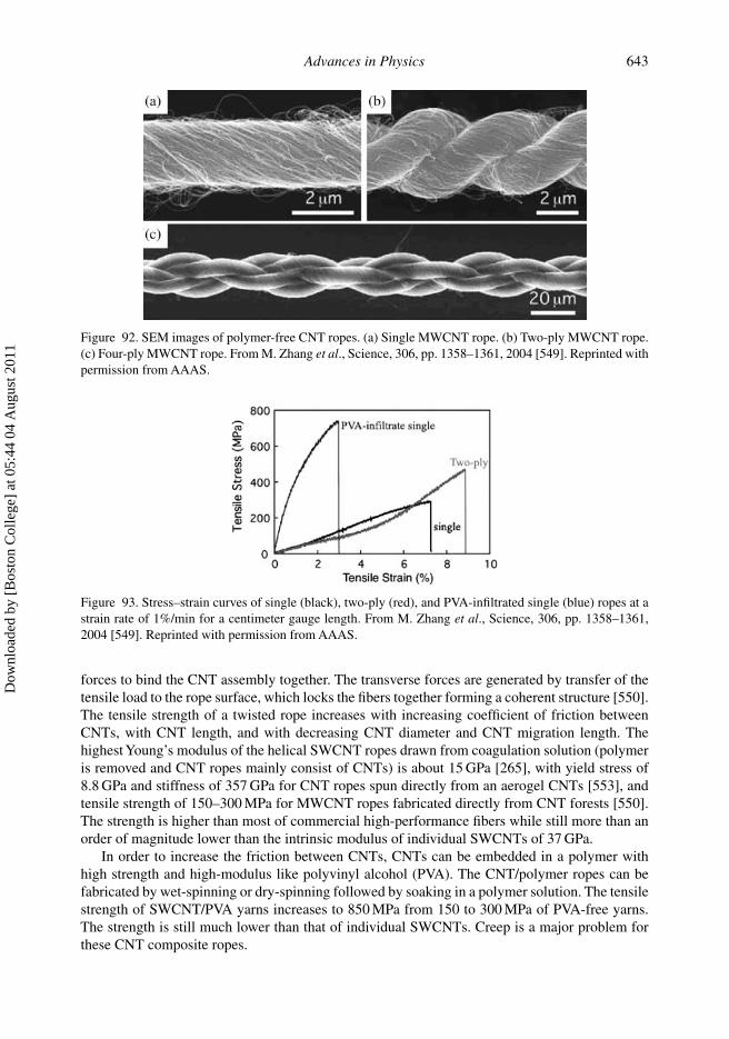
Advances in Physics 643
Figure 92. SEM images of polymer-free CNT ropes. (a) Single MWCNT rope. (b) Two-ply MWCNT rope.(c) Four-ply MWCNT rope. From M. Zhang et al., Science, 306, pp. 1358–1361, 2004 [549]. Reprinted withpermission from AAAS.
Figure 93. Stress–strain curves of single (black), two-ply (red), and PVA-infiltrated single (blue) ropes at astrain rate of 1%/min for a centimeter gauge length. From M. Zhang et al., Science, 306, pp. 1358–1361,2004 [549]. Reprinted with permission from AAAS.
forces to bind the CNT assembly together. The transverse forces are generated by transfer of thetensile load to the rope surface, which locks the fibers together forming a coherent structure [550].The tensile strength of a twisted rope increases with increasing coefficient of friction betweenCNTs, with CNT length, and with decreasing CNT diameter and CNT migration length. Thehighest Young’s modulus of the helical SWCNT ropes drawn from coagulation solution (polymeris removed and CNT ropes mainly consist of CNTs) is about 15 GPa [265], with yield stress of8.8 GPa and stiffness of 357 GPa for CNT ropes spun directly from an aerogel CNTs [553], andtensile strength of 150–300 MPa for MWCNT ropes fabricated directly from CNT forests [550].The strength is higher than most of commercial high-performance fibers while still more than anorder of magnitude lower than the intrinsic modulus of individual SWCNTs of 37 GPa.
In order to increase the friction between CNTs, CNTs can be embedded in a polymer withhigh strength and high-modulus like polyvinyl alcohol (PVA). The CNT/polymer ropes can befabricated by wet-spinning or dry-spinning followed by soaking in a polymer solution. The tensilestrength of SWCNT/PVA yarns increases to 850 MPa from 150 to 300 MPa of PVA-free yarns.The strength is still much lower than that of individual SWCNTs. Creep is a major problem forthese CNT composite ropes.
Dow
nloa
ded
by [
Bos
ton
Col
lege
] at
05:
44 0
4 A
ugus
t 201
1

644 Y. Lan et al.
Twisted polymer fibers consisting of CNTs at less than 10 wt% have also been fabricated. Themechanical strength and modulus are enhanced compared with pure polymer fibers [539]. It isreported that the tensile strength andYoung’s modulus have reached 4.2 and 167 GPa, respectively,in the dry-jet wet spinning poly(p-phenylene benzobisoxazole)/SWCNT ropes (SWCNT: 10 wt%)[554]. When the SWCNTs are lower than 2.1 wt%, the additive of SWCNTs does not enhance themechanical properties [555].
In order to avoid creeping, two-ply ropes are fabricated by over-twisting a single rope(Figure 92(b)), and four-ply ropes by oppositely twisting a two-ply rope (Figure 92(c)), andeven knitted or knotted ropes are fabricated. Higher tensile strength values of 250–460 MPa aremeasured for two-ply yarns, while only 150–300 MPa for single-ply yarns (Figure 93).
Figure 94 shows Young’s modulus of CNT ropes with different diameters. Both experimentaldata [556] and theoretical analysis [557] indicate that the tensile modulus depends strongly onthe diameter of the CNT ropes because of the creeping between CNTs. With the increase in ropediameters,Young’s modulus is diminished by approximately 68% when upscaling from nanoscaleto microscale.
5.1.2. TEM grids
The continuous CNT sheets with centimeters in width and tens of nanometers in thickness canbe fabricated by spinning methods [262,549,558] as described in Section 2.2.3.2. The CNTs areparallel-aligned in the drawing direction and end-to-end jointed to form a continuous thin film,having a much better alignment than the as-synthesized CNT arrays [558]. These aligned CNTsheets are transparent and highly conductive [264,558,559], as a good candidate for TEM gridsupporting films.
Figure 95 shows the morphologies of a TEM grid. In the fabrication of TEM grids, fourlayers of CNT thin sheets are directly cross-stacked layer by layer on TEM copper grids, then anorganic solvent is dispensed on the sheets to bond the sheets onto the copper grid, following aCNT sheet cutting by a focused laser beam. The ultrathin CNT sheets cover the copper grid baseand regular networks with numerous holes are formed. The holes are mostly less than 1 μm indiameter, and the nanometer-sized holes are more than 60% of all holes. Considering the goodelectrical conductivity and mechanical strength of CNTs, these TEM grids are ideal tools for thecharacterization of nanomaterials. HRTEM image of nanoparticles (Figure 95(c)) shows a clear
Figure 94. Young’s modulus of SWCNT ropes with helical array geometry. (a) Experimental data and (b)theoretical data. (a) Reprinted figure with permission from J.-P. Salvetat et al., Physical Review Letters 82,p. 944–947, 1999 [556]. Copyright (1999) by the American Physical Society. (b) Reprinted with permissionfrom R.B. Pipes and P. Hubert, Nano Letters, 3, 2003, pp. 239–243. Copyright (2003) American ChemicalSociety.
Dow
nloa
ded
by [
Bos
ton
Col
lege
] at
05:
44 0
4 A
ugus
t 201
1

Advances in Physics 645
Figure 95. Morphologies of a TEM grid with CNT sheet as a supporting film. (a) SEM image of the CNTsheet over the holes of a copper grid. Inset: optical image of the coated TEM grid with a diameter of 3 mm.(b) TEM image of the CNT sheet covering a hole showing a network morphology. (c) HRTEM image of aCu2S nanoparticle on one side of a nanotube of the TEM grid. Reprinted with permission from L. Zhanget al., Nano Letters, 8, 2008, pp. 2564–2569. Copyright (2008) American Chemical Society.
profile and the fine structures of an individual nanoparticle attached to a CNT of the TEM gridscovered with CNT sheets.
In comparison with conventional TEM holey carbon grids, the TEM grids with CNT sheetshave some advanced characteristics resulting from the excellent intrinsic physical properties ofCNTs [560]. Firstly, the CNT has strong adsorbability – it can easily adsorb small nanoparticles andensure them to be suspended stably during TEM observation. Secondly, due to good conductivityof MWCNTs, the CNT sheet also has good electrical conductivity (bulk resistivity is about 3.8 ×10⁻⁴ � m). Thirdly, because of the fixed interspace between sidewalls of the MWCNTs, i.e.,∼0.34 nm, the CNT grid can be a standard sample for calibration of HRTEM magnification andsize measurement of specimens. In addition, the CNT sheet has a better thermal stability than thatof the conventional amorphous carbon film.
5.1.3. Mechanical tapes
Replicating the multiscale structure of micron-size setae and nanometer-size spatulas of geckolizard feet using microfabricated MWCNTs, CNT arrays can translate weak van der Waals inter-actions into enormous attractive forces [561]. The CNT block arrays (50–500 μm patches) aresynthesized from photolithographic patterns as described in Section 2.1.3. Each block array worksas micron-size setae and consists of thousands of individual MWCNTs, the nano-sized spatulas.These patterned CNT arrays can stick to both hydrophobic and hydrophilic surfaces with a maxi-mum shear stress of 36 N/cm2, nearly four times higher than the gecko foot and 10 times higherthan polymer pillars. The shear forces supported by the patterned CNT arrays are very stable andtime-independent.
5.2. Electrical devices
SWCNTs are metallic or semiconducting according to their structures. The electronic propertiesof perfect MWCNTs are rather similar to those of perfect SWCNTs. In the 1D electronic structure,electrons transport in metallic SWCNTs and MWCNTs over long nanotube lengths, carrying highcurrent densities [304]. So much research work has been carried out to add random CNTs intovarious composites to enhance electrical conductivity. Depending on the composite matrix, con-ductivities of 0.01–10 S/m can be obtained for 5 wt% MWCNT loading or 0.1–0.2 wt% SWCNTloading in polymers. Such high conductivities and dissipate electrostatic charges [318,495], having
Dow
nloa
ded
by [
Bos
ton
Col
lege
] at
05:
44 0
4 A
ugus
t 201
1
646 Y. Lan et al.
potential applications in electrostatic discharge and electromagnetic radio interference protection.The preparation and electrical properties of random CNT composites are reviewed [340]. Theelectrical conductivity of CNT composites also depends on the alignment as well as the concen-tration of CNTs [562,563]. Here we review several electrical applications of aligned CNTs withoutmatrices.
5.2.1. Low κ dielectrics
Electrically insulating layers are required in integrated circuits on semiconductor substrates toreduce the coupling capacitance of interconnects. The low κ materials with low relative dielectricconstants are employed as the insulating layers in integrated circuits to reduce the coupling capaci-tance. Amorphous silicon dioxide with or without fluorine, hydrogen, or alkyl groups is often usedas the dielectric to electrically insulate the metallic interconnects from one another. The relativedielectric constant of electrically insulating layers can be reduced further by introducing cavitiesinto the low-κ materials. The κ-value decreases linearly with the cavity volume fraction. Thesimulation calculations demonstrate that the effective κ value is also affected by the morphologyof the cavities. If elongated and oriented pores are used, it is possible to reduce significantly theeffective κ value without increasing the proportion of the cavity volume in a dielectric. With thesame proportion of cavity volume, a reduction of 13% is achieved with a cavity aspect ratio of4:1 and a reduction of 20% is achieved with a cavity aspect ratio of 24:1 when the cavities areoriented perpendicularly to an electric field.
CNTs have a high aspect ratio and can be used to introduce elongated, oriented pores into alow-κ dielectric to further reduce the effective κ value of the dielectric.
In a typical procedure, aligned CNT forests are grown on a desired surface using PECVDmethods as described in Section 2.1.3. Silicon dioxide is deposited between and on top of CNTs.The oxide is removed by mechanical polishing or by a dry-etch process to expose the CNTs. In orderto create the oriented pores in the oxide, the CNTs are subsequently removed by high-temperatureoxidation and/or oxygen or hydrogen plasma.
5.2.2. Random access memory
Aligned CNTs can serve as addressable electromechanical switches arrayed across the surfaceof a microchip, storing hundreds of gigabits of information (Figure 96). When an electric fieldis applied to a nanotube, the electric field causes the CNT flex downward into a depression ontothe chip’s surface, where it contacts metal electrodes (in another design, the CNTs touch othernanotubes [564]). Once bent, the nanotubes maintain their shapes, including when the power isturned off, allowing for a nonvolatile operation. Van der Waals forces hold the switch in placeuntil application of a field of different polarity causes the nanotubes to return to their straightenedpositions. The binary 0 state corresponds to the nanotubes suspended and not making contact withthe electrode (Figure 96(b)). When a transistor turns on, the electrode produces an electric fieldthat causes the aligned CNTs to bend and touch an electrode, a configuration that denotes a 1 state(Figure 96(c)).
5.2.3. Transistors
Figure 97 shows a transistor array made from vertically aligned CNTs grown on a template ofporous aluminum oxide as described in Section 2.1.3.2. In the integrated device, each CNT iselectrically attached to a source electrode (lower electrode in Figure 97(b)) and a drain electrode(upper electrode in Figure 97(b)). The gate electrode is located close to the nanotubes. Current
Dow
nloa
ded
by [
Bos
ton
Col
lege
] at
05:
44 0
4 A
ugus
t 201
1

Advances in Physics 647
Figure 96. RAM made with aligned CNTs [564]. Reprinted from Materials Today, 11, E. Bichoutskaia et al.,pp. 38–43 [565]. Copyright (2008), with permission from Elsevier.
Figure 97. Architecture of a CNT transistor array. (a) Vertically grown CNTs with diameter of 20 nm andheight of 40 nm. (b) Structure of a CNT transistor. (c) Current–voltage diagram of a vertically oriented CNTtransistor at a temperature of 4.2 K. No bias is applied to the gate. Reprinted with permission from W.B.Choi et al., Applied Physics Letters, 79, 2001, pp. 3696–3698 [566]. Copyright (2001), American Instituteof Physics.
flows from the source electrode to the drain electrode and can be switched on or off by applyinga voltage to the gate. Figure 97(c) shows a current–voltage curve of a CNT transistor.
5.3. Thermoacoustic loudspeakers
The thermoacoustic phenomenon was discovered in the late nineteenth century. When an alter-nating current passes through a thin conducting plate or wire, a periodic heating takes place inthe conductor because of Joule’s effect, following the periodic change of the current amplitude.This periodic heating causes a periodic temperature oscillation that heats the surrounding medium(usually air) near the conductor surface, resulting in the contraction and expansion of moleculesnear the conductor while the conductor remains static. The vibrating movement of the moleculesresults in the generation of an acoustic wave. In a conventional thermoacoustic device (thermo-phone), the acoustic element is a thin metal film such as a gold film with a thickness of 285 nm[567] and a platinum strip with a thickness of 1.8 μm [568].
Dow
nloa
ded
by [
Bos
ton
Col
lege
] at
05:
44 0
4 A
ugus
t 201
1

648 Y. Lan et al.
To obtain appreciable amplitudes of acoustic waves, it is essential that the conductor be verythin and its heat capacity be very low to conduct the produced heat at a high rate [568]. CNTshave an extremely low heat capacity and good thermal conductivity, CNT sheets can be heatedup to 2000 ◦C in less than 1 ms, and the sheet temperature synchronizes with electrical currents ina wide frequency range of 1–105 Hz [403]. The thickness of CNT sheets is also very small, lessthan microns. So CNT sheets are one of the best candidates for thermoacoustic devices.
Figure 98(a) shows a CNT sheet loudspeaker. The CNT sheets are directly drawn out from CNTforests consisting of superaligned CNTs with diameters of 10 nm. Such a dry-spinning methodis described in Section 2.2.3.2. The thickness of the CNT sheet is of tens of nanometers. TheCNT sheet loudspeaker is formed by directly putting the CNT sheet on two electrodes. When asinusoidal voltage is applied across the two electrodes, clear and loud tones are emitted from theCNT sheet.
Figure 98(b) shows the input voltage and the output sound pressure. The output sound pressureis measured by a microphone near the CNT sheet. It is noted that the frequency of the soundpressure doubles that of the input voltage, as observed in a conventional thermophone. When analternating current passes through the CNT sheet, the CNT sheet is heated twice, once duringpositive and once during negative half-cycles of the alternating current, resulting in a double-frequency temperature oscillation, as well as a double frequency sound pressure [569]. The outputsound with doubled frequency always sounds strange. In order to reproduce human voice andmusic with normal frequency without introducing the double frequency effect, a direct currentbias must be superimposed to the alternating current. When the strength of the direct currentis several times higher than that of the alternating current, the double frequency effect can benegligible [568]. Then the CNT sheet loudspeaker can possess all the functions of a voice-coilloudspeaker (Figure 98(b)) [569].
The CNT sheet loudspeaker can generate sound in a wide frequency range (1–105 Hz). The highsound pressure level increases with increasing frequency and the sound pressure is proportionalto the input power. The sound pressure produced by the CNT sheet under an alternating currentcan be expressed as [568]
Prms =( √
αρ0
2√
πT0
√f
Cs
)Pinput
r(7)
in an open system (a more accurate while more complex expression is derived in references[569,570]), in which Cs is the heat capacity per unit area of the CNT sheet, f the frequency of
Figure 98. Thermoacoustic CNT loudspeaker. (a) Optical image of a thermoacoustic CNT sheet loudspeaker.(b) Real-time signals of the input voltage of a CNT thin-film loudspeaker and the output sound pressure fromthe microphone, indicating that the frequency of the sound pressure doubles that of the input voltage. Thephase shift between the input voltage and the output sound pressure signal is primarily due to the soundpropagation from the CNT sheet to the microphone detector. Reprinted with permission from L. Xiao et al.,Nano Letters, 8, 2008, pp. 4539–4545 [569]. Copyright (2008) American Chemical Society.
Dow
nloa
ded
by [
Bos
ton
Col
lege
] at
05:
44 0
4 A
ugus
t 201
1

Advances in Physics 649
sound, Pinput = I2R the input electrical power proportional to the square of applied root-mean-square (rms) current I = I0 sin(ωt), R the resistance of the CNT sheet, r the distance between thethin CNT sheet conductor and the sound pressure detector (microphone), ρ0, T0, and α the density,average temperature, and thermal diffusivity of the surrounding medium, respectively, and Prms
the root-mean-square sound pressure.Equation (7) indicates that the produced sound pressure decreases rapidly with distance. Usu-
ally the temperature of the CNT sheet is also a sinusoid of time, and the temperature wavespropagate into the atmosphere on either side. The periodic temperature change in the thin boundarylayer near the CNT sheets account for the sound vibration. Calculation shows that the temperaturewaves propagate into the working medium and are practically extinguished after one wavelength(27 μm in air and 2.0 μm in water) has been traversed [568].
According to Equation (7), the sound pressure generated by CNT sheet loudspeaker is 260times higher than that generated by a conventional thermophone with a 700 nm thick Pt film asthe acoustic element, corresponding to a 48 dB difference in the sound pressure level [569]. Themeasured sound pressure level of the CNT loudspeaker is over 100 dB at high frequencies, higherthan the conventional thermoacoustic device with a gold film of 285 nm in thickness as the acousticelement (63 dB) [567].
The pressure generation efficiency coefficient ξ = (√
αρ0/2√
πT0)(√
f /Cs) is affected bymany parameters [571], such as (1) the ability of the CNT sheet to be rapidly electrically heatedand then to transfer heat to the surrounding medium at high rates, thereby returning to a start-ing temperature within the excitation cycle; (2) the working medium, which enables rapid heattransfer while minimizing effective increase in the heat capacity of the projector material, andsurviving the possible extreme temperature of the CNT sheets; and (3) possible packaging, whichprovides protection for the CNT sheets and efficient transmission of internal acoustic oscillationto external locations. Theoretical calculation indicates that a CNT sheet working in argon has ahigher generation coefficient than that in air or in helium while 100 times higher than that workingin liquids, such as water, methanol, and ethanol [571].
Besides the freestanding CNT sheet loudspeaker, CNT sheets are also encapsulated into anargon- or air-filled chamber. Such encapsulated CNT loudspeakers can be used in liquids, such aswater [571]. In the small enclosure, the sound pressure is Prms = (
√αρ0T 1/4
surf)/(V0TaveCsf 3/2) ×Pinput, where Tsurf is the temperature of the surface of the CNT sheet, Tave the average temperatureof the filled gas, and V0 the volume of the enclose [568]. The produced pressure causes a vibrationof the attached enclosure windows with a resonant frequency fr (fr = 3.28 kHz when workingin air and 1050 Hz when immersed in water [571]). The highest sound pressure level is over130 dB, 30 dB higher than that exposed to air. The total energy conversion efficiency of the argon-encapsulated thermoacoustic device is 0.2%, while that of CNT freestanding sheet device in airdoes not exceed 0.001%.
5.4. Electrochemical/chemical storage devices
Systems for electrochemical energy storage and conversion include batteries, fuel cells, and elec-trochemical capacitors [572]. Although the mechanisms are different, the common features arethat the energy-providing processes take place at the phase boundary of the electrode/electrolyteinterface and that electron and ion transports are separated. All of them consist of two electrodesin contact with an electrolyte solution. Figure 99 is a simplified Ragone-diagram disclosing thespecific power and specific energy of these three electrochemical storage systems. Fuel cells canbe considered to be high-energy systems and supercapacitors to be high-power systems whilebatteries have intermediate power and energy characteristics. Although no single electrochemicalpower source can match the characteristics of the internal combustion engine (high power and high
Dow
nloa
ded
by [
Bos
ton
Col
lege
] at
05:
44 0
4 A
ugus
t 201
1

650 Y. Lan et al.
Figure 99. Simplified Ragone diagram of the energy storage domains for the electrochemical energy conver-sion systems compared to the internal combustion engine, turbines, and conventional capacitors. Reprintedwith permission from M. Winter and R.J. Brodd, Chemical Reviews, 104, 2004, pp. 4245–4270 [572].Copyright (2004) American Chemical Society.
energy), some hybrid electrochemical power sources combining fuel cells (deliver high energy) andsupercapacitors (provide high power) will be competitive with regard to the combustion enginesand turbines in the future.
Most favorable electrodes in these electrochemical storage systems are porous electrodes withlarge surface areas and low polarization. The porous structures of electrodes increase the surfacearea for reaction and shorten the diffusion path lengths to the reaction sites. The location of thereaction site inside a porous electrode is strongly dependent on the characteristics of the electrodestructures and the reactions themselves. The key parameters include conductivity, porosity, andpore size of the electrodes besides the characteristics of the electrolyte and the reactants [572].The effectiveness of a porous electrode can be estimated from the active surface area S and thepenetration depth of the reaction process into the porous electrode.
CNTs are the electrode material of choice because a CNT combines a large surface areawetted by an electrolyte, a high electrical conductivity, and a high chemical, mechanical, andelectrochemical stability. The electrochemical behaviors of CNTs have been studied [422,442,443,448,479–481,484,573,574] because of their good electrical conductivity/chemical inertness/widepotential range. Below we discuss the application of aligned CNT arrays as porous electrodes inthese chemical storage devices. Because of the large electrochemically accessible surface area ofCNT arrays, combined with their high electrical conductivity and useful mechanical properties,CNT arrays are attractive as electrodes for devices that use electrochemical double-layer chargeinjection [318].
5.4.1. Fuel cells
Fuel cells, one kind of electrochemical energy storage devices, are made up of three sandwichedsegments similar to ultracapacitors and batteries: an anode, an electrolyte, and a cathode, in areaction cell. Different from ultracapacitors and batteries in which the energy is stored in thecells and consumed, electricity is produced inside the fuel cells through the reactions between an
Dow
nloa
ded
by [
Bos
ton
Col
lege
] at
05:
44 0
4 A
ugus
t 201
1

Advances in Physics 651
external fuel and an oxidant in the presence of an electrolyte. At the anode, a catalyst, usually Ptnanoparticles, oxidizes the fuel, usually hydrogen, hydrocarbons, and alcohols, turning the fuelinto positively charged ions and negatively charged electrons. The electrolyte (usually composedof aqueous alkaline solution, polymer membrane, phosphoric acid, molten carbonate, and solidoxide substrates) blocks the transportation of electrons while conducting ions. On the cathode,the ions traveling through the electrolyte are re-united with the electrons passing through a loadduring a reaction with an oxidant, such as oxygen, chlorine, and chlorine dioxide, to producewater or carbon dioxide. In a typical fuel cell using methanol as the fuel, methanol is oxidized toproduce ions and electrons at the anode in a polymer electrolyte:
CH3OH + H2Ocatalyst−→ 6H+ + 6e− + CO2 (8)
and oxygen combines with electrons and H+ ions at the cathode catalyst surface to form water:
O2 + 4H+ + 4e− −→ 2H2O (9)
Fuel cells can operate continuously as long as the fuels and the oxidants are well maintained [572].Platinum and platinum alloys seem to be the best choice of catalysts for the electroreduction
of oxygen in an acidic media [575]. The catalytic nanoparticles are deposited on porous materials,like activated carbon, as electrodes. The electrocatalytic activity of platinum catalyst is dependenton many factors [576]. Among them, the good properties of the catalyst supports, such as highsurface area and good electrical properties, are essential for a Pt catalyst to highly promote catalyticactivities [577]. The large accessible surface area, low resistance, and high stability of CNTs[578,579] suggest that CNTs are suitable materials for electrodes and catalyst supports in fuelcells. The nanoparticles with electrocatalytic activities may decorate the external walls or beencapsulated in the interior of the CNTs [104]. Several papers have studied the electrocatalyticproperties of tangled and substrate-free CNTs [423,580–584]. More details of electrocatalyticactivities using CNT electrodes are reviewed recently [585,586]. Pt has been deposited on activatedSWCNTs or MWCNTs by chemical reduction methods and the resultant electrodes show goodelectrocatalytic properties for hydrogenation [580], and oxygen reduction [423,582]. Below wereview the electrocatalytic properties of CNT arrays.
Figure 100 shows the electrocatalytic properties of a Pt/CNT electrode for oxygen reductionreaction investigated by linear sweep voltammetry in a 0.1 M H2SO4 aqueous solution. The well-aligned CNT arrays are synthesized by the PECVD method (see Section 2.1.3) on a titaniumsubstrate as the working electrode. The CNT diameters are 50–70 nm and the lengths are 3–4 μm[578]. Experiments show that no O2 reduction current is observed using CNT array electrodesor using graphite electrodes over the studied potential range [578]. This means that the CNTarrays and the graphite substrate result in no obvious electrocatalytic activities. Then Pt catalystsare deposited on the CNT arrays using a potential-step electrodeposition method. Pt catalyticnanoparticles are also deposited on a conventional graphite electrode for comparison. After Ptcoating, electrocatalytic activity is observed (Figure 100). Figure 100(a) and (b) are the linearsweep voltammograms of Pt/CNT and Pt/graphite electrodes at different Pt deposition charges,respectively. For Pt/CNT electrodes, a large oxygen reduction current is observed at 0.36V, whichis the typical potential for oxygen electroreduction on platinum catalysts in a H2SO4 solution[587]. The specific current, defined by peak current density (mA/cm2) per unit of depositioncharge (μC/cm2) [587], is used to evaluate the electrocatalytic activity of Pt catalysts for oxygenreduction activities. When the Pt loading mass is low (deposition charge: 9.744 μC/cm2), thespecific current of the Pt/CNT electrode (solid curve in Figure 100(a)) is 0.41 mA/μC, whichis 1.4 times as large as that of a Pt/graphite electrode (dashed curve in Figure 100(a)). At a
Dow
nloa
ded
by [
Bos
ton
Col
lege
] at
05:
44 0
4 A
ugus
t 201
1

652 Y. Lan et al.
Figure 100. The linear sweep voltammograms of Pt/CNT arrays in N2 saturated 0.1 M H2SO4 aqueoussolution. For comparison, the voltammograms of platinum-electrodeposited graphite disk electrode (geom-etry area 1.71 cm2 prepared at the same conditions) are also plotted as dashed curves. (a) Pt nanoparticlesdisperse individually on CNT walls with a deposition charge of 9.744 μC/cm2. (b) Pt nanofilm is depositedon individual CNTs with a deposition charge of 572.5 μC/cm2 while the coated CNTs huddle together toform bundles of 2–10 CNTs. Linear sweep rate is 200 mV/s. Reprinted from Carbon, 42, H. Tang et al., pp.191–197 [578]. Copyright (2004), with permission from Elsevier.
high deposition charge (572.5 μC/cm2), the specific current of the Pt/CNT electrode (solid curvein Figure 100(b)) is almost twice as large as that of a Pt/graphite electrode (dashed curve inFigure 100(b)). These results imply that the Pt/CNT electrodes possess higher electrocatalyticactivities for oxygen reduction.
The increase in the O2 reduction activity of Pt/CNT array electrodes may be attributed tothe following two factors: (i) high dispersion of Pt nanoparticles on the 3D structure of CNTelectrodes can provide large acceptable surface areas of Pt nanoparticles for oxygen reduction;(ii) the particular structure and electrical properties of CNT arrays may be beneficial to the elec-trocatalytic reduction of oxygen. A previous study on the dissociation of adsorptive oxygen onthe surface of CNTs suggested that CNTs have the ability to promote electron-transfer reactions[574]. Additionally, the activity of the catalyst, which could be involved in the interaction betweenmetallic catalyst and catalyst support, can be strongly affected by the properties of the supportingmaterials. These results imply that well-aligned CNT arrays may be a good candidate for thecathodic catalyst supports in fuel cells.
Dow
nloa
ded
by [
Bos
ton
Col
lege
] at
05:
44 0
4 A
ugus
t 201
1
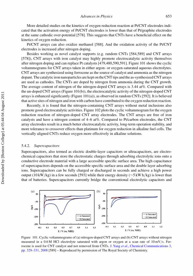
Advances in Physics 653
More detailed studies on the kinetics of oxygen reduction reaction at Pt/CNT electrodes indi-cated that the activation energy of Pt/CNT electrodes is lower than that of Pt/graphite electrodesat the same cathodic over-potential [578]. This suggests that CNTs have a beneficial effect on thekinetics of oxygen reduction.
Pt/CNT arrays can also oxidize methanol [588]. And the oxidation activity of the Pt/CNTelectrodes is increased after nitrogen doping.
Besides working as novel catalyst supports (e.g. random CNTs [584,589] and CNT arrays[578]), CNT arrays with iron catalyst may highly promote electrocatalytic activity themselvesafter nitrogen doping and can replace Pt catalysts [479,480,590,591]. Figure 101 shows the cyclicvoltammograms for CNT arrays taken in either argon- or oxygen-saturated aqueous electrolytes.CNT arrays are synthesized using ferrocene as the source of catalyst and ammonia as the nitrogendopant. The catalytic iron nanoparticles are kept on the CNT tips and the as-synthesized CNT arraysare used as cathodes. The CNTs are doped by nitrogen from ammonia during the CNT growth.The average content of nitrogen of the nitrogen-doped CNT arrays is 3.44 at%. Compared withthe un-doped CNT arrays (Figure 101(b)), the electrocatalytic activity of the nitrogen-doped CNTarrays is enhanced significantly (Figure 101(a)), as observed in random CNTs [592]. It is believedthat active sites of nitrogen and iron with carbon have contributed to the oxygen reduction reaction.
Recently, it is found that the nitrogen-containing CNT arrays without metal inclusions alsopromote good electrocatalytic activities. Figure 102 plots the cyclic voltammogram for the oxygenreduction reaction of nitrogen-doped CNT array electrodes. The CNT arrays are free of ironcatalysts and have a nitrogen content of 4–6 at%. Compared to Pt/carbon electrodes, the CNTarray electrodes result in a much better electrocatalytic activity, long-term operation stability, andmore tolerance to crossover effects than platinum for oxygen reduction in alkaline fuel cells. Thevertically aligned CNTs reduce oxygen more effectively in alkaline solutions.
5.4.2. Supercapacitors
Supercapacitors, also termed as electric double-layer capacitors or ultracapacitors, are electro-chemical capacitors that store the electrostatic charges through adsorbing electrolytic ions onto aconductive electrode material with a large accessible specific surface area. The high capacitanceof supercapacitors depends on the accessible specific surface area and the double layer adsorbingions. Supercapacitors can be fully charged or discharged in seconds and achieve a high poweroutput (10 kW/kg) in a few seconds [593] while their energy density (∼5 kW h/kg) is lower thanthat of batteries. Supercapacitors currently bridge the conventional electrolytic capacitors and
Figure 101. Cyclic voltammograms of (a) nitrogen-doped CNT arrays and (b) CNT arrays without nitrogenmeasured in a 0.6 M HCl electrolyte saturated with argon or oxygen at a scan rate of 10 mV/s. Fer-rocene is used for CNT catalyst and not removed from CNTs. J. Yang et al., Chemical Communications 3,pp. 329–331, 2008 [589] – Reproduced by permission of The Royal Society of Chemistry.
Dow
nloa
ded
by [
Bos
ton
Col
lege
] at
05:
44 0
4 A
ugus
t 201
1

654 Y. Lan et al.
Figure 102. The cyclic voltammogram for the oxygen reduction reaction of CNT array electrodes before(solid curves) and after (dotted curves) a continuous potentiodynamic swept for 100,000 cycles in anair-saturated 0.1 M KOH solution at 25◦C. The CNT array electrodes are free of metal catalysts. The proper-ties of Pt/carbon electrodes are also plotted as a reference. From G. Gong et al., Science, 323, pp. 760–764,2009 [591]. Reprinted with permission from AAAS.
traditional batteries because they combine the unique properties of conventional capacitors (highpower density) and that of traditional batteries (high energy density) [594].
Supercapacitors consist of two electrodes immersed in or impregnated with an electrolytesolution with a semi-permeable membrane serving as a separator that prevents electrical contactbetween the two electrodes. Figure 103 schematically illustrates a supercapacitor made of CNTarray electrodes. The supercapacitors store the electrostatic charges by reversible absorption ofelectrolytic ions on active materials with large accessible specific surface areas. Usually activatedcarbon and porous carbon are used as the active materials because of their large specific surfaceareas (1000–3500 m2/g). When an electric potential is applied to the electrodes, a potential dif-ference is created at the electrode–electrolyte interface because of the charge separation frompolarization. This electrostatic interface consists of a double-layer between the ions in the elec-trolyte and the electrical charges on the electrode. The capacitance of a supercapacitor is generally
Figure 103. Schematic of electrochemical double-layer capacitor based on [594]. The membrane thicknessis several nanometers. The potential difference is only several volts.
Dow
nloa
ded
by [
Bos
ton
Col
lege
] at
05:
44 0
4 A
ugus
t 201
1

Advances in Physics 655
assumed to follow that of a parallel-plate capacitor based on the Helmholtz model1 [595]:
C = ε0εrA
d, (10)
where εr is the dielectric constant of the electrolyte, ε0 the permittivity of vacuum, A the specificsurface area of the electrode accessible to the electrolyte ions, and d the effective thickness ofthe electrical double-layer. In the supercapacitors, the electrical energy is stored as the electro-static charges based on the separation of charged species in an electrical double-layer across theelectrode–solution interfaces and there is no faradic (redox) reaction.
The active materials with high specific surface area and electrically conducting electron col-lectors produce high capacitances. In conventional supercapacitors, activated carbon or glassycarbon are employed as electrodes. The graphitic carbon is a good candidate for supercapacitorsbecause of their high conductivity, high electrochemical stability, and porous structures. Up tonow, the double-layer capacitance of porous carbon with a broad distribution of pore sizes reaches100–200 F/g in organic electrolytes and exceeds 370 F/g in aqueous electrolytes [596]. The largersurface area of activated carbon promotes absorption of ions on electrodes, leading to an enhancedcapacitance [597] and store more energy than the conventional capacitors.
It is observed that the capacitance of supercapacitors is maximum when the electrode size isclose to the ion size [598], confirming the capacitance contribution from pores with sizes smallerthan the solvated ion size. CNTs are aligned regularly, possessing regular pore structures, andadjustable pore sizes, and therefore are the best candidates for supercapacitor electrodes.
The CNT arrays have larger surface areas than activated carbon to store electron charges insupercapacitors. In addition, the CNT site density can be adjusted to store elementary charges,such as electrons, and consequently the capacitance may be increased considerably.
Supercapacitors have giant capacitances in comparison with those of ordinary dielectric-based capacitors. Like ordinary capacitors, CNT supercapacitors are typically comprised of twoelectrodes separated by an electrically insulating material, which is ionically conducting in elec-trochemical devices [599,600]. The capacitance depends on the separation between the charges onthe electrodes and the countercharges in the electrolyte that contributed mostly to the capacitance.Very large capacitances result from the large CNT surface area accessible to the electrolyte. Thesecapacitances depend on the surface area of the CNT array. The capacitances of 180 and 102 F/gare achieved for random SWCNT electrodes and MWCNT electrodes, respectively. It is typicallybetween ∼15 and ∼200 F/g when random CNTs are employed [599,600]. The capacitances comefrom the large amounts of charge injection when only a few volts are applied. The application ofCNT arrays as capacitors are reviewed recently [594,596,601,602].
The CNT array electrodes possess lower ion diffusion resistance, higher electrical conductivity,larger pores, and more regular pore structure than the electrodes consisting of random CNTs. So,the CNT array electrodes have higher capacitances, lower resistances, and better rate performances[601].
The CNT array electrodes can be fabricated ex situ or in situ. In ex situ procedures, CNT arraysare grown by CVD methods described in Section 1.4. Then they are detached from the substrates,re-attached onto an electrically conductive current collector by binding [603], soldering, or surfacetension, to form a CNT array electrode. The CNT array electrodes can also be fabricated fromrandom CNTs by self-assembly processes [604]. In in situ procedures described in Section 2.1,a CNT array can be directly grown on a current collector to form an electrode [605–607]. Theprocedure is a one-step process, and the electrical resistance between the CNT array and thecurrent collector is relatively low.
CNT arrays store energy by the electrochemical double-layer formed on the surfaces of eachCNT in the array. Since the capacitive properties of the array-like CNT membranes were studied
Dow
nloa
ded
by [
Bos
ton
Col
lege
] at
05:
44 0
4 A
ugus
t 201
1

656 Y. Lan et al.
[481], capacitance of 18 F/g was obtained in 6 M KOH electrolytes using a 400 μm long CNTarray directly grown on a metallic alloy [606], and 35 F/g was obtained in 6 M KOH using aCNT array embedded in cellulose [608]. The cyclic voltammetry curves indicate that the contactresistance between the CNTs and the current collector is low. Beside the aqueous electrolytes,organic electrolytes are also tested. Capacitances of 22 F/g in ionic liquid electrolyte [608], 80 F/gin 1 M Et4NBF4/PC electrolyte using SWCNT arrays [609], 10–15 F/g in organic electrolytesat an extremely high current density of 200A/g [610], 83 F/g in organic electrolytes using aDWCNT array of 300 μm in length grown on a conductive Si substrate [611], and 27 F/g inorganic electrolytes [607] are reported.
Experimental results indicate that the CNT array electrodes possess lower ion diffusivity resis-tances and higher electrical conductivities, better rate performances, and higher capacitances thanrandom CNTs because of the regular pore structure and the large pore size of CNT arrays.
Although CNT array electrodes possess a higher rate capability than any other electrochemicalelectrode materials, their capacitances are moderate, i.e., 10–80 F/g [607,611,612], lower thanthe activated carbon and pseudo-capacitive materials. The moderate capacitance should comefrom the medium specific surface area of CNTs (120–500 m2/g), lower than that of active carbon(1000–3500 m2/g) [596]. In order to improve the power and cycle performances of CNT arrayelectrodes, pseudo-capacitive materials (including conducting polymers, such as polyaniline [613],polypyrrole, and polythiophene, metal oxides, such as ruthenium oxide, manganese oxide [614],NiO, and Fe3O4, and nitrides, such as vanadium nitride) are deposited on the CNT surface toform CNT composite electrodes. In these CNT composite capacitors, CNTs serve as an effectivesupport for pseudo-capacitive materials because of the excellent mechanical properties of CNTs.At the same time, the CNTs conduct electrons due to superior electrical properties. These pseudo-capacitive (or termed redox supercapacitive) materials can be fast and reversible redoxed onthe CNT surfaces or near-surface for charge storage and the pseudo-capacitance is faradic. Forexample, the ruthenium oxidation states in ruthenium oxide can react in electrolyte as [593]
RuO2 + xH+ + xe− ↔ RuO2−x(OH)x, 0 ≤ x ≤ 2 (11)
The continuous change of x during H+ insertion leads to a pseudo-capacitive behavior with ionadsorption. The charge storage mechanism of manganese oxide is based on the surface absorptionof electrolyte cations and proton incorporation:
MnO2 + xC+ + yH+ + (x + y)e− ↔ MnOOCxHy (12)
A study in an electrolyte ionic liquid shows that maximum capacitance is produced when the poresize is close to the ionic radius [598]. So the density of CNT array is usually very high with thegap between CNTs being a few nanometers. So, the conducting polymers and inorganic materialsare usually electrodeposited on CNT arrays, like PANI [613] and MnOx [614].
Such CNT array composites have higher capacitances than CNT arrays and pseudo-capacitivematerials due to the contribution of both double-layer capacitance and pseudo-capacitance(Figure 104). The capacitance of the PANI/CNTA composite is 1030 F/g at a low current densityof 5.9A/g [613], higher than the PANI materials. Compared to the best results from commercialproducts (about 130 F/g), the pseudo-capacitors have much higher energy storage capabilities.
The advantages of CNT arrays as capacitors come from their excellent mechanical properties,electrical conductivity, and good ion conduction owing to the straight conduction pathways [609].
Dow
nloa
ded
by [
Bos
ton
Col
lege
] at
05:
44 0
4 A
ugus
t 201
1

Advances in Physics 657
Figure 104. Specific capacitance of (a) manganese oxide-CNT array (CNTA), manganese oxide-entangledCNT (ECNT), manganese oxide-active carbon (AC), and CNTA versus discharge current density. (b) Polyani-line on CNT array compared with pilyaniline/CNTA. (a) Reprinted with permission from H. Zhang et al.,Nano Letters, 8, 2008, pp. 2664–2668 [614]. Copyright (2008) American Chemical Society. (b) Reprintedfrom Electrochemistry Communications, 10, H. Zhang et al., pp. 1056–1059 [613]. Copyright (2008), withpermission from Elsevier.
5.4.3. Lithium ion batteries
In batteries, electrical energy is generated by conversion of chemical energy via a redox reaction atthe anode and the cathode in a closed system. Unlike in ultracapacitors where the solvent of the elec-trolyte is not involved in the charge storage mechanism, the solvent of the electrolyte contributesto the solid–electrolyte interphase in batteries. The Li-ion batteries, one kind of rechargeable bat-teries, usually consist of an active carbon anode, a lithium–cobalt oxide cathode, and an organicelectrolyte.
Activated carbon is used in the commercial lithium-ion batteries. In order to obtain betterperformance, CNT arrays and CNT array composites are recently studied as electrodes besidesthe random CNTs and random CNT composites.
Figure 105 illustrates such a Li-ion battery consisting of CNT array (composite) electrodes anda Li electrode. The CNT arrays are prepared by the PECVD method described in Section 2.1.3. The
Figure 105. Schematic diagram showing the Li-ion battery devices with CNT array electrode as anode.Reprinted from Electrochemistry Communications, 10, H. Zhang et al., pp. 1056–1059 [613]. Copyright(2008), with permission from Elsevier.
Dow
nloa
ded
by [
Bos
ton
Col
lege
] at
05:
44 0
4 A
ugus
t 201
1

658 Y. Lan et al.
PANI/CNT array composite is used as the lithium-ion battery cathode [613]. The capacity of suchPANI/CNT array composite electrode (98 mA h/g) is higher than that of the PANI/random CNTcomposite electrode (86 mA h/g) [615]. MnOx/CNT array composite electrodes are also used ascathodes [614]. The capacity of MnOx/CNT array composite (246 mA h/g) is also higher than thatof MnOx-based nanostructures. In the CNT array composites, the CNT array framework enhancesthe rate performance of the electrode materials by providing good electrical conductivity andpreserving the benefits of the electrochemica properties of supercapacitive nanomaterials. TheCNT array electrodes can be used as lithium-ion battery anodes [481,601]. The rate and cycleperformance of CNT array electrodes are superior to random CNT electrodes.
5.4.4. Hydrogen storage
CNTs have been long heralded as potentially useful for hydrogen storage. It was reported that theamount of hydrogen desorbed on SWCNTs is 5–10 wt% at room temperature [616–618], closeto the reasonable automotive target of 6.5 wt%. Later, a higher hydrogen storage capacity wasreported and a lot of papers have been published in this field. For example, it was reported thatlithium-doped SWCNTs can absorb 20 wt% of hydrogen at room temperatures under ambientpressures [619]. However, experimental reports of high storage capacities are so controversial thatit is impossible to assess the true potential [318]. Careful experiments indicate that the largestabsorption percentage of hydrogen is less than 0.1 wt% at room temperature in SWCNTs [620],in MWCNTs [620], and in carbon fibers [621]. Recent investigations show only a small reversiblehydrogen uptake for SWCNTs [622]. More efforts are needed in the field, and the application ofCNT arrays in hydrogen storage is still far away from practical applications.
5.5. Electromechanical devices
5.5.1. Actuators
Electromechanical actuators are frequently used in robots and typically comprised of two elec-trodes separated by an electrically insulating material, similar to the supercapacitors. The chargeinjection causes electrode expansions and contractions that can do mechanical work in the elec-tromechanical actuators [623]. The maximum observed isometric actuator stress of SWCNT-sheetactuators is about 26 MPa, 100 times that of the stress generation capability of natural muscles.
5.5.2. Artificial muscles
Actuator materials can convert electrical, chemical, thermal, or photonic energies to mechanicalenergy. Electrostatic attraction and repulsion between two CNTs were used for cantilever-basednanotweezers [624] and electromechanically based logic elements [564] and nanoswitches [625].Macroscaled CNT actuators powered by electricity [623,626,627] or fuel [628] can provide ahundred times higher stress generation than natural muscles [629]. Aligned CNT composites canalso be actuators powered by IR irradiation [630] or by electricity [631], and be of shape memoryfunctions [632,633].
Figure 106 shows the CNT aerogel sheets used as the sole component of artificial muscles.The CNT aerogel sheets are fabricated by the spinning method described in Section 2.2.3.2. Suchmuscles can provide giant elongations and elongation rates of 220% and 3.7 × 10⁴% per second,respectively, at operating temperatures from 80 to 1900 K. The observed voltage dependence ofactuator stroke in the width direction at length center, normalized to the initial width to providegenerated strain W/W0, is shown in Figure 106(c) for single and stacked aerogel ribbons having
Dow
nloa
ded
by [
Bos
ton
Col
lege
] at
05:
44 0
4 A
ugus
t 201
1

Advances in Physics 659
Figure 106.Artificial muscles. (a) Photograph of a rigidly end-supported 50 mm long × 2 mm wide nanotubesheet strip. (b) Same sheet strip expanded in width by applying a 5 kV voltage with respect to ground. (c)Width-direction actuation strain, W/W0 versus applied voltage for N = 1–8 stacks of single aerogel sheetsand for a densified eight-sheet stack, labeled 1 to 8 and 8′, respectively, having L0 = 25 mm and W0 = 2 mm.The universal curve in the inset for this aspect ratio (12.5) shows results for un-densified nanotube sheet stacksthat are normalized with a single-fit parameter R, where the normalization factor is SN = (1/N − R)/(1 − R).From A.E. Aliev et al., Science, 323, pp. 1575–1578, 2009 [634]. Reprinted with permission from AAAS.
the same L0/W0 ratio. W/W0 increases approximately quadratically with applied voltage V ,while a crossover occurs at higher voltages to a weaker dependence, ∼ V 3/2.
5.6. Terahertz sources
CNTs have many properties – from their unique dimensions to an unusual current conductionmechanism – that make them ideal components of electrical circuits. For example, they haveshown to exhibit strong electron–phonon resonances, which indicate that under certain directcurrent bias and doping conditions their current and the average electron velocity, as well asthe electron concentration on the tube, oscillate at terahertz frequencies. These resonances couldpotentially be used to make terahertz sources or sensors.
5.7. Other applications
There are a handful of other applications of assembled CNTs, such as blackbody absorbers [635],vacuum microelectronic sources [361,370], and IR detectors [636,637].
6. Conclusions
In summary, the in situ and ex situ fabrication methods, the physics for alignment, the uniquephysical properties, and the broad application scale of aligned CNTs are reviewed. It has beenclearly demonstrated by numerous publications that PECVD and thermal CVD are frequently themost effective methods to in situ grow aligned CNT arrays with a pre-determined orientation,diameter, length, location, and site density. Depending on the spatial distribution of catalyticnanoparticles on substrates, the aligned CNTs may have 1D or 3D orderings. The mechanismsfor achieving alignment are discussed. Aligned CNTs have found their edges for applications inthermal, electrical, photonic, mechanical, chemical, and biological devices as well as various types
Dow
nloa
ded
by [
Bos
ton
Col
lege
] at
05:
44 0
4 A
ugus
t 201
1

660 Y. Lan et al.
of sensors for gas and bio-specie detections. These applications are reviewed and illustrated basedon the uniqueness of the aligned CNT geometry and the corresponding physical properties due toalignment.
Although there have been extensive research efforts on CNT alignment, the physics and prop-erties, and the broad application possibilities, there still remain tremendous unfinished work andunexplored territories to realize the full potentials of aligned CNTs. It is the hope of the authorsthat this review can generate even broader interests from researchers of all related fields and fromacademic and industrial funding institutions to further explore various applications of alignedCNTs with a grand goal of improving our fundamental scientific understanding and everyday life.
Note1. In fact, the structure of the electric double-layer is more complex than the Helmholtz model. Helmholtz
model states that two layers of opposite charges are formed at the electrode–electrolyte interface and areseparated by an atomic distance. Modified Gouy–Chapman model refers to a diffuse layer consistingof continuous distribution of electrolyte ions (both cations and anions), not a layer consisting of onlycations or only anions, in the electrolyte solution. The modern Stern model combines the Helmoltzmodel with the Gouy–Chapman model to structure two regions of ion distribution: the inner compactlayer (Stern layer) where ions are strongly absorbed by the electrode and an outer diffuse layer definedin the Gouy-Chapman model. The more accurate capacitance is a sum of the capacitances from the tworegions: 1/C = 1/CStern + 1/Cdiff . Both Stern layer contribution Cstern and diffuse layer contributionCdiff are proportional to the specific surface area and depend on the pore size.
Acknowledgements
The work carried out at Boston College was funded by the US Department of Energy undercontract number DOE DE-FG02-00ER45805 (Z.F.R.) and the Defense Threat Reduction Agencyunder a grant HDTRA1-07-1-0015 (Y.C.L.).
For all figures reprinted from American Physical Society material readers may view, browse,and/or download material for temporary copying purposes only, provided these uses are fornoncommercial personal purposes. Except as provided by law, this material may not be furtherreproduced, distributed, transmitted, modified, adapted, performed, displayed, published, or soldin whole or part, without prior written permission from the American Physical Society.
References
[1] S. Iijima, Nature 354 (1991), pp. 56–58.[2] H.W. Kroto, J.R. Heath, S.C. O’Brien, R.F. Curl, and R.E. Smalley, Nature 318 (1985), pp. 162–163.[3] M. Monthioux and V.L. Kuznetsov, Carbon 44 (2006), pp. 1621–1623.[4] T.V. Hughes and C.R. Chambers, US Patent 405480, (1889).[5] L.V. Radushkevich and V.M. Lukyanovich, J. Phys. Chem. Russia 26 (1952), pp. 88–95.[6] A. Oberlin, M. Endo, and T. Koyama, J. Cryst. Growth 32 (1976), pp. 335–349.[7] H.P. Boehm, Carbon 11 (1973) 583–586, IN581–IN585, 587–590.[8] J. Abrahamson, P.G. Wiles, and B.L. Rhoades, 14th Biennial Conference on Carbon, (1979).[9] H.G. Tennent, US Patent 4663230, (1987).
[10] M. Reibold, P. Paufler, A.A. Levin, W. Kochmann, N. Patzke, and D.C. Meyer, Nature 444 (2006),pp. 286–286.
[11] S. Iijima and T. Ichihashi, Nature 363 (1993), pp. 603–605.[12] D. S. Bethune, R. D. Johnson, J. R. Salem, M. S. de Vries, and C. S. Yannoni, Nature 366 (1993),
pp. 123–128.[13] J.A.E. Gibson, Nature 359 (1992), pp. 369–369.
Dow
nloa
ded
by [
Bos
ton
Col
lege
] at
05:
44 0
4 A
ugus
t 201
1

Advances in Physics 661
[14] H.P. Boehm, Carbon 35 (1997), pp. 581–584.[15] X.H. Chen, C.S. Chen, Q. Chen, F.Q. Cheng, G. Zhang, and Z.Z. Chen, Mater. Lett. 57 (2002),
pp. 734–738.[16] P. Chaturvedi, P. Verma, A. Singh, P.K. Chaudhary, Harsh, and P.K. Basu, Defence Sci. J. 58 (2008),
pp. 591–599.[17] K. MacKenzie, O. Dunens, and A.T. Harris, Sep. Purif. Technol. 66 (2009), pp. 209–222.[18] S.K. Pillai, S.S. Ray, and M. Moodley, J. Nanosci. Nanotechnol. 7 (2007), pp. 3011–3047.[19] S.K. Pillai, S.S. Ray, and M. Moodley, J. Nanosci. Nanotechnol. 8 (2008), pp. 6187–6207.[20] X. Song and Y. Fang, Spectrochim. Acta A 67 (2007), pp. 1131–1134.[21] T. Guo, P. Nikolaev,A. Thess, D.T. Colbert, and R.E. Smalley, Chem. Phys. Lett. 243 (1995), pp. 49–54.[22] A. Thess, R. Lee, P. Nikolaev, H. Dai, P. Petit, J. Robert, C. Xu,Y.H. Lee, S.G. Kim, A.G. Rinzler, D.T.
Colbert, G.E. Scuseria, n.D. Tomà, J.E. Fischer, and R.E. Smalley, Science 273 (1996), pp. 483–487.[23] J. Li, C. Papadopoulos, and J. Xu, Nature 402 (1999), pp. 253–254.[24] W.Z. Li, J.G. Wen, and Z.F. Ren, Appl. Phys. Lett. 79 (2001), pp. 1879–1881.[25] A.G. Nasibulin, P.V. Pikhitsa, H. Jiang, D.P. Brown, A.V. Krasheninnikov, A.S. Anisimov, P. Queipo,
A. Moisala, D. Gonzalez, G. Lientschnig, A. Hassanien, S.D. Shandakov, G. Lolli, D.E. Resasco, M.Choi, D. Tomanek, and E.I. Kauppinen, Nat. Nano. 2 (2007), pp. 156–161.
[26] L. Liu, G.Y. Guo, C.S. Jayanthi, and S.Y. Wu, Phys. Rev. Lett. 88 (2002) 217206.[27] G.E. Scuseria, Chem. Phys. Lett. 195 (1992), pp. 534–536.[28] B.C. Satishkumar, P.J. Thomas,A. Govindaraj, and C.N.R. Rao,Appl. Phys. Lett. 77 (2000), pp. 2530–
2532.[29] A.G. Nasibulin, A.S. Anisimov, P.V. Pikhitsa, H. Jiang, D.P. Brown, M. Choi, and E.I. Kauppinen,
Chem. Phys. Lett. 446 (2007), pp. 109–114.[30] W.Z. Li, S.S. Xie, L.X. Qian, B.H. Chang, B.S. Zou, W.Y. Zhou, R.A. Zhao, and G. Wang, Science,
274 (1996), pp. 1701–1703.[31] M. Terrones, N. Grobert, J. Olivares, J.P. Zhang, H. Terrones, K. Kordatos, W.K. Hsu, J.P. Hare,
P.D. Townsend, K. Prassides, A.K. Cheetham, H.W. Kroto, and D.R.M. Walton, Nature 388 (1997),pp. 52–55.
[32] Z.F. Ren, Z.P. Huang, J.W. Xu, J.H. Wang, P. Bush, M.P. Siegal, and P.N. Provencio, Science 282(1998), pp. 1105–1107.
[33] Z.F. Ren, Z.P. Huang, D.Z. Wang, J.G. Wen, J.W. Xu, J.H. Wang, L.E. Calvet, J. Chen, J.F. Klemic,and M.A. Reed, Appl. Phys. Lett. 75 (1999), pp. 1086–1088.
[34] Z.P. Huang, D.L. Carnahan, J. Rybczynski, M. Giersig, M. Sennett, D.Z. Wang, J.G. Wen, K. Kempa,and Z.F. Ren, Appl. Phys. Lett. 82 (2003), pp. 460–462.
[35] K. Kempa, B. Kimball, J. Rybczynski, Z.P. Huang, P.F. Wu, D. Steeves, M. Sennett, M. Giersig,D.V.G.L.N. Rao, D.L. Carnahan, D.Z. Wang, J.Y. Lao, W.Z. Li, and Z.F. Ren, Nano Lett. 3 (2003),pp. 13–18.
[36] S. Fan, M.G. Chapline, N.R. Franklin, T.W. Tombler, A.M. Cassell, and H. Dai, Science 283 (1999),pp. 512–514.
[37] M.S. Dresselhaus, G. Dresselhaus, and P.C. Eklund, The Science of Fullerenes and Carbon Nanotubes,Academic, San Diego, 1996.
[38] R. Saito, G. Dresselhaus, and M.S. Dresselhaus, Physical Properties of Carbon Nanotubes, WorldScientific, 1998.
[39] P.J.F. Harris, Carbon nanotubes and related structures: New materials for the twenty-first century,Cambridge University Press, Cambridge, 1999.
[40] M.S. Dresselhaus, G. Dresselhaus, and P.Avouris, Carbon Nanotubes: Synthesis, Structure, Properties,and Applications, Springer, 2001.
[41] C.N.R. Rao, R. Voggu, and A. Govindaraj, Nanoscale 1 (2009), pp. 96–105.[42] H. Dai, A.G. Rinzler, P. Nikolaev, A. Thess, D.T. Colbert, and R.E. Smalley, Chem. Phys. Lett., 260
(1996), pp. 471–475.[43] M. Audier and M. Coulon, Carbon (1985), pp. 317–323.[44] C. Kane, L. Balents, and M.P.A. Fisher, Phys. Rev. Lett. 79 (1997), p. 5086.[45] N. Hamada, S.-I. Sawada, and A. Oshiyama, Phys. Rev. Lett. 68 (1992), pp. 1579–1581.
Dow
nloa
ded
by [
Bos
ton
Col
lege
] at
05:
44 0
4 A
ugus
t 201
1

662 Y. Lan et al.
[46] R. Saito, M. Fujita, G. Dresselhaus, and M.S. Dresselhaus, Phys. Rev. B 46 (1992), pp. 1804–1811.[47] R. Saito, M. Fujita, G. Dresselhaus, and M.S. Dresselhaus,Appl. Phys. Lett. 60 (1992), pp. 2204–2206.[48] J.W.G. Wildoer, L.C. Venema, A.G. Rinzler, R.E. Smalley, and C. Dekker, Nature 391 (1998), pp. 59–
62.[49] T.W. Odom, J.-L. Huang, P. Kim, and C.M. Lieber, Nature 391 (1998), pp. 62–64.[50] S. Reich, C. Thomsen, and J. Maultzsch, Carbon Nanotubes: Basic Concepts and Physical Properties,
Wiley-VCH, Germany, 2004.[51] S. Hong and S. Myung, Nat. Nano. 2 (2007), pp. 207–208.[52] J.H. Hafner, M.J. Bronikowski, B.R. Azamian, P. Nikolaev, A.G. Rinzler, D.T. Colbert, K.A. Smith,
and R.E. Smalley, Chem. Phys. Lett. 296 (1998), pp. 195–202.[53] G.Y. Xiong, Y. Suda, D.Z. Wang, J.Y. Huang, and Z.F. Ren, Nanotechnology 16 (2005), pp. 532–535.[54] O.M. Dunens, K.J. MacKenzie, and A.T. Harris, Ind. Eng. Chem. Res. 49 (2010), pp. 4031–4035.[55] E. Flahaut, R. Bacsa, A. Peigney, and C. Laurent, Chem. Commun. 12 (2003), pp. 1442–1443.[56] A. Oberlin, M. Endo, and T. Koyama, Carbon 14 (1976), pp. 133–135.[57] Three-dimensional images are created using POV-Ray open-source software (http://www.povray.org).[58] R. Bacon, J. Appl. Phys. 31 (1960), pp. 283–290.[59] H. Cui, X.Yang, M.L. Simpson, D.H. Lowndes, and M. Varela, Appl. Phys. Lett. 84 (2004), pp. 4077–
4079.[60] W.Z. Li, J.G. Wen, and Z.F. Ren, Appl. Phys. A 74 (2002), pp. 397–402.[61] W.Z. Li, J.G. Wen, Y. Tu, and Z.F. Ren, Appl. Phys. A 73 (2001), pp. 259–264.[62] W. Wang, B. Poudel, D.Z. Wang, and Z.F. Ren, J. Am. Chem. Soc. 127 (2005), pp. 18018–18019.[63] Y. Ominami, Q. Ngo, A.J. Austin, H. Yoong, C.Y. Yang, A.M. Cassell, B.A. Cruden, J. Li, and
M. Meyyappan, Appl. Phys. Lett. 87 (2005), pp. 233105–233103.[64] P.R. Bandaru and J. Mater. Sci. 42 (2007), pp. 1809–1818.[65] M.S. Fuhrer, R.J. Nygå, L. Shih, M. Forero, Y.-G. Yoon, M.S.C. Mazzoni, H.J. Choi, J. Ihm, S.G.
Louie, A. Zettl, and P.L. McEuen, Science 288 (2000), pp. 494–497.[66] H. Nishino, R. Nishida, T. Matsui, N. Kawase, and I. Mochida, Carbon 41 (2003), pp. 2819–2823.[67] T. Luo, L. Chen, K. Bao, W. Yu, and Y. Qian, Carbon 44 (2006), pp. 2844–2848.[68] W.Y. Jang, N.N. Kulkarni, C.K. Shih, and Z. Yao, Applied Physics Letters 84 (2004), pp. 1177–1179.[69] Y.F. Hu, X.L. Liang, Q. Chen, L.M. Peng, and Z.D. Hu, Appl. Phys. Lett. 88 (2006) 063113.[70] J. Li, C. Papadopoulos, J.M. Xu, and M. Moskovits, Appl. Phys. Lett. 75 (1999), pp. 367–369.[71] S. Amelinckx, X.B. Zhang, D. Bernaerts, X.F. Zhang, V. Ivanov, and J.B. Nagy, Science 265 (1994),
pp. 635–639.[72] N. Grobert, M. Terrones, S. Trasobares, K. Kordatos, H. Terrones, J. Olivares, J.P. Zhang, P. Redlich,
W.K. Hsu, C.L. Reeves, D.J. Wallis,Y.Q. Zhu, J.P. Hare,A.J. Pidduck, H.W. Kroto, and D.R.M. Walton,Applied Physics A: Materials Science & Processing 70 (2000) 175–183.
[73] H. Hou, Z. Jun, F. Weller, and A. Greiner, Chemistry of Materials 15 (2003), pp. 3170–3175.[74] M. Sano, A. Kamino, J. Okamura, and S. Shinkai, Science 293 (2001), pp. 1299–1301.[75] J. Liu, H. Dai, J.H. Hafner, D.T. Colbert, R.E. Smalley, S.J. Tans, and C. Dekker, Nature 385 (1997),
pp. 780–781.[76] R. Martel, H.R. Shea, and P. Avouris, Nature 398 (1999) 299.[77] J.Q. Hu,Y. Bando, F.F. Xu,Y.B. Li, J.H. Zhan, J.Y. Xu, and D. Golberg, Advanced Materials 16 (2004),
pp. 153–156.[78] S. Iijima, Journal of Crystal Growth 50 (1980), pp. 675–683.[79] N. Sano, H. Wang, M. Chhowalla, I. Alexandrou, and G.A.J. Amaratunga, Nature 414 (2001),
pp. 506–507.[80] M. Burghard, Surf. Sci. Rep. 58 (2005), pp. 1–109.[81] S.G. Louie, Electronic properties, junctions, and defects of carbon nanotubes, in: M.S. Dresselhaus, G.
Dresselhaus, P. Avouris (Eds.) Carbon Nanotubes: Synthesis, Structure, Properties, and Applications,Springer, 2001, pp. 113–146.
[82] Z.Yao, C. Dekker, and P. Avouris, Electronic transport through single-wall carbon nanotubes, in: M.S.Dresselhaus, G. Dresselhaus, P. Avouris (Eds.) Carbon Nanotubes: Synthesis, Structure, Properties,and Applications, Springer, 2001, pp. 147–172.
Dow
nloa
ded
by [
Bos
ton
Col
lege
] at
05:
44 0
4 A
ugus
t 201
1

Advances in Physics 663
[83] L.A.S.O. Forro and N.C. Scho, Physical properties of multi-wall nanotubes, in: M.S. Dresselhaus, G.Dresselhaus, P. Avouris (Eds.) Carbon Nanotubes: Synthesis, Structure, Properties, and Applications,Springer, 2001, pp. 329–390.
[84] J. Bernholc, D. Brenner, M.B. Nardelli, V. Meunier, and C. Roland, Annu. Rev. Mater. Res. 32 (2002),pp. 347–375.
[85] V.N. Popov, Mat. Sci. Eng. R: Rep. 43 (2004), pp. 61–102.[86] M.S. Dresselhaus, G. Dresselhaus, and A. Jorio, Annu. Rev. Mater. Res. 34 (2004), pp. 247–278.[87] R. Saito and H. Kataura, Optical properties and raman spectroscopy of carbon nanotubes, in: M.S. Dres-
selhaus, G. Dresselhaus, and P. Avouris (Eds.) Carbon Nanotubes: Synthesis, Structure, Properties,and Applications, Springer, 2001, pp. 213–246.
[88] H. Dai, Surf. Sci. 500 (2002), pp. 218–241.[89] J. Hone, Phonons and thermal properties of carbon nanotubes, in: M.S. Dresselhaus, G. Dresselhaus, P.
Avouris (Eds.) Carbon Nanotubes: Synthesis, Structure, Properties, and Applications, Springer, 2001,pp. 273–286.
[90] B.I. Yakobson and P. Avouris, Carbon Nanotubes: Synthesis, Structure, Properties, and Applications,in: M.S. Dresselhaus, G. Dresselhaus, P. Avouris (Eds.), Springer, 2001, pp. 287–328.
[91] B. Dóra, M. Gulácsi, F. Simon, and H. Kuzmany, Phys. Rev. Lett. 99 (2007) 166402.[92] K. Hata, D.N. Futaba, K. Mizuno, T. Namai, M.Yumura, and S. Iijima, Science 306 (2004), pp. 1362–
1364.[93] H.W. Zhu, C.L. Xu, D.H. Wu, B.Q. Wei, R. Vajtai, and P.M. Ajayan, Science 296 (2002), pp. 884–886.[94] Z.W. Pan, S.S. Xie, B.H. Chang, C.Y. Wang, L. Lu, W. Liu, W.Y. Zhou, W.Z. Li, and L.X. Qian, Nature,
394 (1998), pp. 631–632.[95] M.-F. Yu, B.S. Files, S. Arepalli, and R.S. Ruoff, Phys. Rev. Lett. 84 (2000), pp. 5552–5555.[96] R.S. Ruoff, J. Tersoff, D.C. Lorents, S. Subramoney, and B. Chan, Nature 364 (1993), pp. 514–516.[97] W.A. de Heer, W.S. Bacsa, Ch, T.A. A, T. Gerfin, R. Humphrey-Baker, L. Forro, and D. Ugarte,
Science, 268 (1995), pp. 845–847.[98] E. Pop, D. Mann, Q. Wang, K. Goodson, and H. Dai, Nano Lett. 6 (2006), pp. 96–100.[99] D. Ugarte, W.S. Bacsa, B. Doudin, L. Forro, and W.A. de Heer, Braz. J. Phys. 26 (1996), pp. 123–127.
[100] A.P. Ramirez, R.C. Haddon, O. Zhou, R.M. Fleming, J. Zhang, S.M. McClure, and R.E. Smalley,Science 265 (1994), pp. 84–86.
[101] J.P. Lu, Phys. Rev. Lett. 74 (1995), pp. 1123–1126.[102] X.K. Wang, R.P.H. Chang, A. Patashinski, and J.B. Ketterson, J. Mater. Res. 9 (1994), pp. 1578–1582.[103] Y. Saito and M. Inagaki, Jpn. J. Appl. Phys. 32 (1993) L954-L957.[104] T.W. Ebbesen and P.M. Ajayan, Nature 358 (1992), pp. 220–222.[105] C. Journet, W.K. Maser, P. Bernier, A. Loiseau, M.L. de la Chapelle, S. Lefrant, P. Deniard, R. Leek,
and J.E. Fischer, Nature 388 (1997), pp. 756–768.[106] M. Ushio, D. Fan, and M. Tanaka, J. Phys. D: Appl. Phys. 27 (1994), pp. 561–566.[107] E.G. Gamaly, Growth mechanism of carbon nanotubes, in: T.W. Ebbesen (Ed.) Carbon nanotubes:
Preparation and properties, Chemical Rubber, Boca Raton, 1997, pp. 164–190.[108] S. Farhat and C.D. Scott, J. Nanosci. Nanotechnol. 6 (2006), pp. 1189–1210.[109] B. Ahmad, M. Ahmad, J.I. Akhter, and N. Ahmad, Materials Letters, 59 (2005), pp. 1585–1588.[110] B. Yakobson and R. Smalley, Am. Sci. 85 (1997), pp. 324–337.[111] T. Guo, P. Nikolaev, A.G. Rinzler, D. Tomanek, D.T. Colbert, and R.E. Smalley, J. Phys. Chem., 99
(1995), pp. 10694–10697.[112] C.D. Scott, S. Arepalli, P. Nikolaev, and R.E. Smalley, Appl. Phys. A 72 (2001), pp. 573–580.[113] Z.Y. Kosakovskaya, JETP Lett. 56 (1992) 26.[114] M. Ge and K. Sattler, Science 260 (1993), pp. 515–518.[115] P.L. Walker, J.F. Rakszawski, and G.R. Imperial, J. Phys. Chem. 63 (1959), pp. 133–140.[116] M. Joseyacaman, M. Miki-Yoshida, N.L. Rendò, and J.G. Santiesteban, Appl. Phys. Lett. 62 (1993),
pp. 657–659.[117] E.T. Thostenson, W.Z. Li, D.Z. Wang, Z.F. Ren, and T.W. Chou, J. Appl. Phys. 91 (2002), pp. 6034–
6037.[118] W.Z. Li, D.Z. Wang, S.X. Yang, J.G. Wen, and Z.F. Ren, Chem. Phys. Lett. 335 (2001), pp. 141–149.
Dow
nloa
ded
by [
Bos
ton
Col
lege
] at
05:
44 0
4 A
ugus
t 201
1

664 Y. Lan et al.
[119] J.B. Nagy, G. Bister,A. Fonseca, D. Mehn, Z. Konya, I. Kiricsi, Z.E. Horvath, and L.P. Biro, J. Nanosci.Nanotechnol. 4 (2004), pp. 4326–4345.
[120] S. Helveg, C. Lopez-Cartes, J. Sehested, P.L. Hansen, B.S. Clausen, J.R. Rostrup-Nielsen, F. Abild-Pedersen, and J.K. Norskov, Nature 427 (2004), pp. 426–429.
[121] H. Zhu, K. Suenaga, A. Hashimoto, K. Urita, K. Hata, and S. Iijima, Small 1 (2005), pp. 1180–1183.[122] F. Ding, K. Bolton, and A. Rosan, J. Phys. Chem. B 108 (2004), pp. 17369–17377.[123] R.T.K. Baker, M.A. Barber, P.S. Harris, F.S. Feates, and R.J. Waite, J. Catal. 26 (1972), pp. 51–62.[124] M. Audier and M. Coulon, Carbon 23 (1985), pp. 317–323.[125] M. Endo, K. Takeuchi, K. Kobori, K. Takahashi, H.W. Kroto, and A. Sarkar, Carbon, 33 (1995),
pp. 873–881.[126] J.-C. Charlier, A. De Vita, X. Blase, and R. Car, Science 275 (1997), pp. 647–649.[127] M. Yudasaka, R. Kikuchi, Y. Ohki, E. Ota, and S. Yoshimura, Appl. Phys. Lett. 70 (1997), pp. 1817–
1818.[128] J.C. Charlier and S. Iijima, Growth mechanisms of carbon nanotubes, in: M.S. Dresselhaus, G. Dres-
selhaus, P. Avouris (Eds.) Carbon Nanotubes: Synthesis, Structure, Properties, and Applications,Springer, 2001, pp. 55–81.
[129] T.W. Ebbesen, Carbon nanotubes: Preparation and properties, (CRC Publisher) Boca Raton, 1997.[130] J.M. Calderon Moreno and M. Yoshimura, J. Am. Chem. Soc. 123 (2001), pp. 741–742.[131] Y. Gogotsi, J.A. Libera, and M. Yoshimura, J. Mater. Res. 15 (2000), pp. 2591–2594.[132] J. Liu, M. Shao, X. Chen, W. Yu, X. Liu, and Y. Qian, J. Am. Chem. Soc. 125 (2003), pp. 8088–8089.[133] Y. Jiang,Y. Wu, S. Zhang, C. Xu, W.Yu,Y. Xie, andY. Qian, J. Am. Chem. Soc. 122 (2000), pp. 12383–
12384.[134] W. Wang, S. Kunwar, J.Y. Huang, D.Z. Wang, and Z.F. Ren, Nanotechnology 16 (2005), pp. 21–23.[135] W. Wang, B. Poudel, D.Z. Wang, and Z.F. Ren, J. Am. Chem. Soc. 127 (2005), pp. 18018–18019.[136] J.K. Vohs, J.J. Brege, J.E. Raymond, A.E. Brown, G.L. Williams, and B.D. Fahlman, J. Am. Chem.
Soc. 126 (2004), pp. 9936–9937.[137] W. Wang, J.Y. Huang, D.Z. Wang, and Z.F. Ren, Carbon 43 (2005), pp. 1328–1331.[138] S. Liu, J. Yue, and R.J. Wehmschulte, Nano Lett. 2 (2002), pp. 1439–1442.[139] W.R. Davis, R.J. Slawson, and G.R. Rigby, Nature 171 (1953), pp. 756–756.[140] M.J. Height, J.B. Howard, J.W. Tester, and J.B. Vander Sande, Carbon 42 (2004), pp. 2295–2307.[141] W. Hu, D. Gong, Z. Chen, L. Yuan, K. Saito, C.A. Grimes, and P. Kichambare, Appl. Phys. Lett. 79
(2001), pp. 3083–3085.[142] R.L. Vander Wal, G.M. Berger, and L.J. Hall, J. Phys. Chem. B 106 (2002), pp. 3564–3567.[143] W.K. Hsu, J. Hare, M.Terrones, H. Kroto, D.R.Walton, and P.J. Harris, Nature 377 (1995), pp. 687–687.[144] W.K. Hsu, M. Terrones, J.P. Hare, H. Terrones, H.W. Kroto, and D.R.M. Walton, Chem. Phys. Lett.
262 (1996), pp. 161–166.[145] H.J. Dai, Nanotube growth and characterization, in: M.S. Dresselhaus, G. Dresselhaus, P. Avouris
(Eds.) Carbon Nanotubes: Synthesis, Structure, Properties, and Applications, Springer, 2001, pp.29–53.
[146] M. Terrones, Annu. Rev. Mater. Res. 33 (2003), pp. 419–501.[147] E. Jiran and C. Thompson, J. Electron. Mater. 19 (1990), pp. 1153–1160.[148] E. Jiran and C.V. Thompson, Thin Solid Films 208 (1992), pp. 23–28.[149] L. Rayleigh, Proceedings of the London Mathematical Society, 1–10 (1878), pp. 4–13.[150] G. Zhang, D. Mann, L. Zhang, A. Javey, Y. Li, E. Yenilmez, Q. Wang, J.P. McVittie, Y. Nishi, J.
Gibbons, and H. Dai, Proc. Nat. Acad. Sci. U.S.A. 102 (2005), pp. 16141–16145.[151] J. Kong, H.T. Soh, A.M. Cassell, C.F. Quate, and H. Dai, Nature 395 (1998), pp. 878–881.[152] R. Andrews, D. Jacques, A.M. Rao, F. Derbyshire, D. Qian, X. Fan, and E.C. Dickey, J. Chen, Chem.
Phys. Lett. 303 (1999), pp. 467–474.[153] S. Sato, A. Kawabata, M. Nihei, and Y. Awano, Chem. Phys. Lett. 382 (2003), pp. 361–366.[154] G.-Y. Xiong, D.Z. Wang, and Z.F. Ren, Carbon 44 (2006), pp. 969–973.[155] A. Cao, V.P. Veedu, X. Li, Z. Yao, M.N. Ghasemi-Nejhad, and P.M. Ajayan, Nat. Mater. 4 (2005)
pp. 540–545.
Dow
nloa
ded
by [
Bos
ton
Col
lege
] at
05:
44 0
4 A
ugus
t 201
1

Advances in Physics 665
[156] S. Chakrabarti, T. Nagasaka, Y. Yoshikawa, L. Pan, and Y. Nakayama, Jpn. J. Appl. Phys. 45 (2006),pp. L720–L722.
[157] X. Li, A. Cao, Y.J. Jung, R. Vajtai, and P.M. Ajayan, Nano Lett. 5 (2005), pp. 1997–2000.[158] L. Zhu, D.W. Hess, and C.-P. Wong, J. Phys. Chem. B 110 (2006), pp. 5445–5449.[159] Y. Zhang, A. Chang, J. Cao, Q. Wang, W. Kim, Y. Li, N. Morris, E. Yenilmez, J. Kong, and H. Dai,
Appl. Phys. Lett. 79 (2001), pp. 3155–3157.[160] L.X. Benedict, S.G. Louie, and M.L. Cohen, Phys. Rev. B 52 (1995), pp. 8541–8549.[161] A. Ural, Y. Li, and H. Dai, Appl. Phys. Lett. 81 (2002), pp. 3464–3466.[162] E. Joselevich and C.M. Lieber, Nano Lett. 2 (2002), pp. 1137–1141.[163] I. Radu, Y. Hanein, and D.H. Cobden, Nanotechnology 15 (2004), p. 473.[164] R.S. Johnson, G. Lucovsky, and I. Baumvol, J. Vac. Sci. Technol. A 19 (2001), pp. 1353–1360.[165] J.G. Wen, Z.P. Huang, D.Z. Wang, J.H. Chen, S.X. Yang, Z.F. Ren, J.H. Wang, L.E. Calvet, J. Chen,
J.F. Klemic, and M.A. Reed, J. Mater. Res. 16 (2001), pp. 3246–3253.[166] C. Bower, W. Zhu, S. Jin, and O. Zhou, Appl. Phys. Lett. 77 (2000), pp. 830–832.[167] A. Nojeh, A. Ural, R.F. Pease, and H. Dai, J. Vac. Sci. Technol., B 22 (2004), pp. 3421–3425.[168] Y. Gao, Y.S. Zhou, W. Xiong, M. Mahjouri-Samani, M. Mitchell, and Y.F. Lu, Appl. Phys. Lett., 95
(2009) 143117.[169] A. Ismach and E. Joselevich, Nano Lett. 6 (2006), pp. 1706–1710.[170] Y. Tu, Y. Lin, and Z.F. Ren, Nano Lett. 3 (2003), pp. 107–109.[171] Y. Wang, J. Rybczynski, D.Z. Wang, K. Kempa, Z.F. Ren, W.Z. Li, and B. Kimball, Appl. Phys. Lett.,
85 (2004), pp. 4741–4743.[172] K.B.K.Teo, D.B. Hash, R.G. Lacerda, N.L. Rupesinghe, M.S. Bell, S.H. Dalal, D. Bose,T.R. Govindan,
B.A. Cruden, M. Chhowalla, G.A.J.Amaratunga, M. Meyyappan, andW.I. Milne, Nano Lett., 4 (2004),pp. 921–926.
[173] C.L. Cheung, A. Kurtz, H. Park, and C.M. Lieber, J. Phys. Chem. B 106 (2002), pp. 2429–2433.[174] H.C. Choi, S. Kundaria, D. Wang, A. Javey, Q. Wang, M. Rolandi, and H. Dai, Nano Lett. 3 (2003),
pp. 157–161.[175] Y. Li, W. Kim, Y. Zhang, M. Rolandi, D. Wang, and H. Dai, J. Phys. Chem. B 105 (2001), pp. 11424–
11431.[176] C. Hinderling, Y. Keles, T. Stöckli, H.F. Knapp, T. de los Arcos, P. Oelhafen, I. Korczagin, M.A.
Hempenius, G.J. Vancso, R. Pugin, and H. Heinzelmann, Adv. Mater. 16 (2004), pp. 876–879.[177] Z.P. Huang, J.W. Xu, Z.F. Ren, J.H. Wang, M.P. Siegal, and P.N. Provencio, Appl. Phys. Lett. 73
(1998), pp. 3845–3847.[178] Y. Tu, Z.P. Huang, D.Z. Wang, J.G. Wen, and Z.F. Ren, Appl. Phys. Lett. 80 (2002), pp. 4018–4020.[179] M. Chhowalla, K.B.K. Teo, C. Ducati, N.L. Rupesinghe, G.A.J. Amaratunga, A.C. Ferrari, D. Roy,
J. Robertson, and W.I. Milne, J. Appl. Phys. 90 (2001), pp. 5308–5317.[180] V.I. Merkulov, D.H. Lowndes,Y.Y. Wei, G. Eres, and E. Voelkl, Appl. Phys. Lett. 76 (2000), pp. 3555–
3557.[181] M.P. Zach and R.M. Penner, Adv. Mater. 12 (2000), pp. 878–883.[182] J.V. Zoval, R.M. Stiger, P.R. Biernacki, and R.M. Penner, J. Phys. Chem. 100 (1996), pp. 837–844.[183] G. Sandmann, H. Dietz, and W. Plieth, J. Electroanal. Chem. 491 (2000), pp. 78–86.[184] H. Liu and R.M. Penner, J. Phys. Chem. B 104 (2000), pp. 9131–9139.[185] J.V. Zoval, J. Lee, S. Gorer, and R.M. Penner, J. Phys. Chem. B 102 (1998), pp. 1166–1175.[186] S.H. Jo, Y. Tu, Z.P. Huang, D.L. Carnahan, D.Z. Wang, and Z.F. Ren, Appl. Phys. Lett. 82 (2003),
pp. 3520–3522.[187] T.A. El-Aguizy, J.-h. Jeong,Y.-B. Jeon, W.Z. Li, Z.F. Ren, and S.-G. Kim, Appl. Phys. Lett. 85 (2004),
pp. 5995–5997.[188] J.S. Suh and J.S. Lee, Appl. Phys. Lett. 75 (1999), pp. 2047–2049.[189] W.J. Yu, Y.S. Cho, G.S. Choi, and D. Kim, Nanotechnology 16 (2005), pp. S291–S295.[190] L. Nilsson, O. Groening, C. Emmenegger, O. Kuettel, E. Schaller, L. Schlapbach, H. Kind, J.M.
Bonard, and K. Kern, Appl. Phys. Lett. 76 (2000), pp. 2071–2073.[191] J. Rybczynski, U. Ebels, and M. Giersig, Colloids Surf., A 219 (2003), pp. 1–6.
Dow
nloa
ded
by [
Bos
ton
Col
lege
] at
05:
44 0
4 A
ugus
t 201
1

666 Y. Lan et al.
[192] J. Rybczynski, K. Kempa,Y. Wang, Z.F. Ren, J.B. Carlson, B.R. Kimball, and G. Benham, Appl. Phys.Lett. 88 (2006) 203122.
[193] J. Rybczynski, D. Banerjee,A. Kosiorek, M. Giersig, and Z.F. Ren, Nano Lett. 4 (2004), pp. 2037–2040.[194] A. Kosiorek, W. Kandulski, P. Chudzinski, K. Kempa, and M. Giersig, Nano Lett. 4 (2004), pp. 1359–
1363.[195] X. Wang, C.J. Summers, and Z.L. Wang, Nano Lett. 4 (2004), pp. 423–426.[196] X.D. Wang, E. Graugnard, J.S. King, Z.L. Wang, and C.J. Summers, Nano Lett. 4 (2004), pp. 2223–
2226.[197] K.J. Mysels, Langmuir 2 (1986), pp. 423–428.[198] S. Huang, X. Cai, C. Du, and J. Liu, J. Phys. Chem. B 107 (2003), pp. 13251–13254.[199] S. Huang, X. Cai, and J. Liu, J. Am. Chem. Soc. 125 (2003), pp. 5636–5637.[200] S. Huang, Q. Fu, L. An, and J. Liu, Phys. Chem. Chem. Phys. 6 (2004), pp. 1077–1079.[201] S. Huang, B. Maynor, X. Cai, and J. Liu, Adv. Mater. 15 (2003), pp. 1651–1655.[202] B.H. Hong, J.Y. Lee, T. Beetz,Y. Zhu, P. Kim, and K.S. Kim, J.Am. Chem. Soc. 127 (2005), pp. 15336–
15337.[203] W. Zhou, Z. Han, J. Wang, Y. Zhang, Z. Jin, X. Sun, Y. Zhang, C. Yan, and Y. Li, Nano Lett. 6 (2006),
pp. 2987–2990.[204] Z. Jin, H. Chu, J. Wang, J. Hong, W. Tan, and Y. Li, Nano Lett. 7 (2007), pp. 2073–2079.[205] Y. Li, D. Mann, M. Rolandi, W. Kim, A. Ural, S. Hung, A. Javey, J. Cao, D. Wang, E. Yenilmez, Q.
Wang, J.F. Gibbons, Y. Nishi, and H. Dai, Nano Lett. 4 (2004), pp. 317–321.[206] Z. Yu, S. Li, and P.J. Burke, Chem. Mater. 16 (2004), pp. 3414–3416.[207] L. Huang, B. White, M.Y. Sfeir, M. Huang, H.X. Huang, S. Wind, J. Hone, and S. O’Brien, J. Phys.
Chem. B 110 (2006), pp. 11103–11109.[208] C. Kocabas, M. Shim, and J.A. Rogers, J. Am. Chem. Soc. 128 (2006), pp. 4540–4541.[209] E. Joselevich, H. Dai, J. Liu, K. Hata, and A.H. Windle, Carbon nanotube synthesis and organization,
in Carbon Nanotubes, Topics in Applied Physics, A. Jorio, G. Dresselhaus and M.S. Dresselhaus. eds.,Springer Berlin / Heidelberg, 2008, pp. 101–164.
[210] M. Su,Y. Li, B. Maynor, A. Buldum, J.P. Lu, and J. Liu, J. Phys. Chem. B 104 (2000), pp. 6505–6508.[211] M. Tominaga, A. Ohira, A. Kubo, I. Taniguchi, and M. Kunitake, Chem. Commun. 2004 (2004),
pp. 1518–1519.[212] V. Derycke, R. Martel, M. Radosavljevic, F.M. Ross, and P. Avouris, Nano Lett. 2 (2002), pp. 1043–
1046.[213] L.B. Ruppalt, P.M. Albrecht, and J.W. Lyding, J. Vac. Sci. Technol., B 22 (2004), pp. 2005–2007.[214] Q. Yu, G. Qin, H. Li, Z. Xia, Y. Nian, and S.-S. Pei, J. Phys. Chem. B 110 (2006), pp. 22676–22680.[215] N. Ishigami, H. Ago, T. Nishi, K.-i. Ikeda, M. Tsuji, T. Ikuta, and K. Takahashi, J. Am. Chem. Soc.,
130 (2008), pp. 17264–17265.[216] W. Zhou, L. Ding, S. Yang, and J. Liu, J. Am. Chem. Soc. 132 (2005), pp. 336–341.[217] S. Han, X. Liu, and C. Zhou, J. Am. Chem. Soc. 127 (2005), pp. 5294–5295.[218] H. Ago, K. Imamoto, N. Ishigami, R. Ohdo, K.-i. Ikeda, and M. Tsuji, Appl. Phys. Lett. 90 (2007)
123112.[219] H. Ago, K. Nakamura, K.-i. Ikeda, N. Uehara, N. Ishigami, and M. Tsuji, Chem. Phys. Lett. 408
(2005), pp. 433–438.[220] A. Rutkowska, D. Walker, S. Gorfman, P.A. Thomas, and J.V. Macpherson, J. Phys. Chem. C, 113
(2009), pp. 17087–17096.[221] H. Ago, N. Uehara, K.-i. Ikeda, R. Ohdo, K. Nakamura, and M. Tsuji, Chem. Phys. Lett. 421 (2006),
pp. 399–403.[222] T. Ozel, D. Abdula, E. Hwang, and M. Shim, ACS Nano 3 (2009), pp. 2217–2224.[223] A. Ismach, L. Segev, E. Wachtel, and E. Joselevich, Angew. Chem. Int. Ed. 43 (2004), pp. 6140–6143.[224] H. Ago, K. Imamoto, T. Nishi, M. Tsuji, T. Ikuta, K. Takahashi, and M. Fukui, J. Phys. Chem. C, 113
(2009), pp. 13121–13124.[225] H. Ago, T. Nishi, K. Imamoto, N. Ishigami, M. Tsuji, T. Ikuta, and K. Takahashi, J. Phys. Chem. C,
114 (2010), pp. 12925–12930.
Dow
nloa
ded
by [
Bos
ton
Col
lege
] at
05:
44 0
4 A
ugus
t 201
1

Advances in Physics 667
[226] N.Yoshihara, H. Ago, K. Imamoto, M. Tsuji, T. Ikuta, and K. Takahashi, J. Phys. Chem. C 113 (2009),pp. 8030–8034.
[227] C.M. Orofeo, H. Ago, N. Yoshihara, and M. Tsuji, Appl. Phys. Lett. 94 (2009) 053113.[228] T. Kamimura and K. Matsumoto, Applied Physics Express 2 (2009) 015005.[229] C. Kocabas, S.-H. Hur, A. Gaur, M.A. Meitl, M. Shim, and J.a.A. Rogers, Small 1 (2005), pp. 1110–
1116.[230] A. Ismach, D. Kantorovich, and E. Joselevich, J. Am. Chem. Soc. 127 (2005), pp. 11554–11555.[231] H.I. Smith and D.C. Flanders, Appl. Phys. Lett. 32 (1978), pp. 349–350.[232] R.A. Segalman, H. Yokoyama, and E.J. Kramer, Adv. Mater. 13 (2001), pp. 1152–1155.[233] B. Zhang, G. Hong, B. Peng, J. Zhang, W. Choi, J.M. Kim, J.-Y. Choi, and Z. Liu, J. Phys. Chem. C,
113 (2009), pp. 5341–5344.[234] K.-H. Lee, J.-M. Cho, and W. Sigmund, Appl. Phys. Lett. 82 (2003), pp. 448–450.[235] N. Kumar, W. Curtis, and J.-i. Hahm, Appl. Phys. Lett. 86 (2005), p. 173101.[236] M.H. Kuang, Z.L. Wang, X.D. Bai, J.D. Guo, and E.G. Wang, Appl. Phys. Lett. 76 (2000), pp. 1255–
1257.[237] X.Q. Chen, T. Saito, H. Yamada, and K. Matsushige, Appl. Phys. Lett. 78 (2001), pp. 3714–
3716.[238] K. Yamamoto, S. Akita, and Y. Nakayama, Jpn. J. Appl. Phys. 35 (1996), pp. L917–L918.[239] K. Bubke, H. Gnewuch, M. Hempstead, J. Hammer, and M.L.H. Green, Appl. Phys. Lett. 71 (1997),
pp. 1906–1908.[240] J. Chung, K.-H. Lee, J. Lee, and R.S. Ruoff, Langmuir 20 (2004), pp. 3011–3017.[241] C. Kocabas, M.A. Meitl, A. Gaur, M. Shim, and J.A. Rogers, Nano Lett. 4 (2004), pp. 2421–2426.[242] J. Heremans, C.H. Olk, and D.T. Morelli, Phys. Rev. B 49 (1994), pp. 15122–15125.[243] D.K. Yoon, S.R. Lee, Y.H. Kim, S.M. Choi, and H.T. Jung, Adv. Mater. 18 (2006), pp. 509–513.[244] K. Kordás, T. Mustonen, G. Toth, J. Vahakangas, A. Uusimaki, H. Jantunen, A. Gupta, K.V. Rao,
R. Vajtai, and P.M. Ajayan, Chem. Mater. 19 (2007), pp. 787–791.[245] G. Korneva, H. Ye, Y. Gogotsi, D. Halverson, G. Friedman, J.-C. Bradley, and K.G. Kornev, Nano
Lett., 5 (2005), pp. 879–884.[246] C. Gao, W. Li, H. Morimoto, Y. Nagaoka, and T. Maekawa, J. Phys. Chem. B 110 (2006), pp. 7213–
7220.[247] S.C. Youn, D.-H. Jung, Y.K. Ko, Y.W. Jin, J.M. Kim, and H.-T. Jung, J. Am. Chem. Soc. 131 (2009),
pp. 742–748.[248] M.A. Correa-Duarte, M. Grzelczak, V. Salgueirino-Maceira, M. Giersig, L.M. Liz-Marzan, M. Farle,
K. Sierazdki, and R. Diaz, J. Phys. Chem. B 109 (2005), pp. 19060–19063.[249] M.F. Lin and K.W.K. Shung, Phys. Rev. B 52 (1995), pp. 8423–8438.[250] D.A. Walters, M.J. Casavant, X.C. Qin, C.B. Huffman, P.J. Boul, L.M. Ericson, E.H. Haroz, M.J.
O’Connell, K. Smith, D.T. Colbert, and R.E. Smalley, Chem. Phys. Lett. 338 (2001), pp. 14–20.[251] X.L. Xie, Y.W. Mai, and X.P. Zhou, Mat. Sci. Eng. R-Reports 49 (2005), pp. 89–112.[252] W.Z. Li, J.G. Wen, M. Sennett, and Z.F. Ren, Chem. Phys. Lett. 368 (2003), pp. 299–306.[253] P.M. Ajayan, O. Stephan, C. Colliex, and D. Trauth, Science 265 (1994), pp. 1212–1214.[254] L. Jin, C. Bower, and O. Zhou, Appl. Phys. Lett. 73 (1998), pp. 1197–1199.[255] M. Ichida, S. Mizuno, H. Kataura, Y. Achiba, and A. Nakamura, Appl. Phys. A 78 (2004), pp. 1117–
1120.[256] Y. Kim, N. Minami, and S. Kazaoui, Appl. Phys. Lett. 86 (2005), p. 073103.[257] X. Yuan, A.F.T. Mak, K.W. Kwok, B.K.O. Yung, and K. Yao, J. Appl. Polym. Sci. 81 (2001), pp. 251–
260.[258] M. Zhang, S. Fang, A.A. Zakhidov, S.B. Lee, A.E. Aliev, C.D. Williams, K.R. Atkinson, and
R.H. Baughman, Science 309 (2005), pp. 1215–1219.[259] M.B. Bazbouz and G.K. Stylios, Eur. Polym. J. 44 (2008), pp. 1–12.[260] N. Behabtu, M.J. Green, and M. Pasquali, Nano Today 3 (2008), pp. 24–34.[261] X. Zhang, Q. Li, T.G. Holesinger, P.N. Arendt, J. Huang, P.D. Kirven, T.G. Clapp, R.F. DePaula,
X. Liao, Y. Zhao, L. Zheng, D.E. Peterson, and Y. Zhu, Adv. Mater. 19 (2007), pp. 4198–4201.
Dow
nloa
ded
by [
Bos
ton
Col
lege
] at
05:
44 0
4 A
ugus
t 201
1

668 Y. Lan et al.
[262] F. Ko, Y. Gogotsi, A. Ali, N. Naguib, H. Ye, G.L. Yang, C. Li, and P. Willis, Adv. Mater. 15 (2003),pp. 1161–1165.
[263] Y.-L. Li, I.A. Kinloch, and A.H. Windle, Science 304 (2004), pp. 276–278.[264] L.M. Ericson, H. Fan, H. Peng, V.A. Davis, W. Zhou, J. Sulpizio, Y. Wang, R. Booker, J. Vavro, C.
Guthy, A.N.G. Parra-Vasquez, M.J. Kim, S. Ramesh, R.K. Saini, C. Kittrell, G. Lavin, H. Schmidt,W.W. Adams, W.E. Billups, M. Pasquali, W.-F. Hwang, R.H. Hauge, J.E. Fischer, and R.E. Smalley,Science 305 (2004), pp. 1447–1450.
[265] B. Vigolo, A. Penicaud, C. Coulon, C.E.D. Sauder, R.E. Pailler, C. Journet, P. Bernier, and P. Poulin,Science 290 (2000), pp. 1331–1334.
[266] P. Poulin, B. Vigolo, and P. Launois, Carbon 40 (2002), pp. 1741–1749.[267] Y. Huang, X. Duan, Q. Wei, and C.M. Lieber, Science 291 (2001), pp. 630–633.[268] S.J. Oh, Y. Cheng, J. Zhang, H. Shimoda, and O. Zhou, Appl. Phys. Lett. 82 (2003), pp. 2521–2523.[269] S.G. Rao, L. Huang, W. Setyawan, and S. Hong, Nature 425 (2003), pp. 36–37.[270] K.M. Seemann, J. Ebbecke, and A. Wixforth, Nanotechnology 17 (2006), p. 4529.[271] Y. Wang, D. Maspoch, S. Zou, G.C. Schatz, R.E. Smalley, and C.A. Mirkin, P. Natl. Acad. Sci. USA,
103 (2006), pp. 2026–2031.[272] A.V. Melechko, V.I. Merkulov, T.E. McKnight, M.A. Guillorn, K.L. Klein, D.H. Lowndes, and
M.L. Simpson, J. Appl. Phys. 97 (2005) 041301.[273] M. Meyyappan, L. Delzeit, A. Cassell, and D. Hash, Plasma Sources Sci. Technol. 12 (2003),
pp. 205–216.[274] K.C. Park, S.H. Lim, J.H. Moon, H.S. Yoon, J. Jang, D. Pribat, and Y. Bonnassieux, J. Korean Phys.
Soc. 45 (2004), pp. S833–S385.[275] Y. Wang, Ph. D Thesis. Nanophotonics of vertically aligned carbon nanotubes: two-dimensional
photonic crystals and optical dipole antenna, Boston College, Chestnut Hill, 2006.[276] Y. Wang, S.H. Jo, S. Chen, D.Z. Wang, and Z.F. Ren, Nanotechnology 17 (2006), pp. 501–505.[277] S. Hofmann, G. Csànyi, A.C. Ferrari, M.C. Payne, and J. Robertson, Phys. Rev. Lett. 95 (2005)
036101–036104.[278] S. Hofmann, C. Ducati, J. Robertson, and B. Kleinsorge, Appl. Phys. Lett. 83 (2003), pp. 135–137.[279] E.J. Bae, Y.-S. Min, D. Kang, J.-H. Ko, and W. Park, Chem. Mater. 17 (2005), pp. 5141–5145.[280] X. Wang, K. Kempa, Z.F. Ren, and B. Kimball, Appl. Phys. Lett. 84 (2004), pp. 1817–1819.[281] J.H. Choi, T.Y. Lee, S.H. Choi, J.-H. Han, J.-B. Yoo, C.-Y. Park, T. Jung, S. Yu, W. Yi, I.T. Han,
and J.M. Kim, Thin Solid Films 435 (2003), pp. 318–323.[282] S.H. Lim, K.C. Park, J.H. Moon, H.S. Yoon, D. Pribat, Y. Bonnassieux, and J. Jang, Thin Solid Films,
515 (2006), pp. 1380–1384.[283] J.H. Choi, T.Y. Lee, S.H. Choi, J.-H. Han, J.-B. Yoo, C.-Y. Park, T. Jung, S.G. Yu, W. Yi, I.-T. Han,
and J.M. Kim, Diamond Relat. Mater. 12 (2003), pp. 794–798.[284] J.R. Roth, Industrial Plasma Engineering, Bristol: Institute of Physics Publishing, 1995.[285] J.D. Fowlkes, A.V. Melechko, K.L. Klein, P.D. Rack, D.A. Smith, D.K. Hensley, M.J. Doktycz, and
M.L. Simpson, Carbon 44 (2006), pp. 1503–1510.[286] F. Silly and M.R. Castell, Appl. Phys. Lett. 87 (2005) 063106.[287] H. Zhou, D. Kumar, A. Kvit, A. Tiwari, and J. Narayan, J. Appl. Phys. 94 (2003), pp. 4841–4846.[288] M.W. Geis, D.C. Flanders, and H.I. Smith, Appl. Phys. Lett. 35 (1979), pp. 71–74.[289] A.L. Giermann and C.V. Thompson, Appl. Phys. Lett. 86 (2005) 121903.[290] Y.-J. Oh, C.A. Ross, Y.S. Jung, Y. Wang, and C.V. Thompson, Small 5 (2009), pp. 860–865.[291] T.E. McKnight, A.V. Melechko, D.W. Austin, T. Sims, M.A. Guillorn, and M.L. Simpson, J. Phys.
Chem. B 108 (2004), pp. 7115–7125.[292] S. Hong, Y.-H. Shin, and J. Ihm, Jpn. J. Appl. Phys. 41 (2002), pp. 6142–6144.[293] S. Reich, L. Li, and J. Robertson, Chem. Phys. Lett. 421 (2006), pp. 469–472.[294] S. Reich, L. Li, and J. Robertson, Phys. Rev. B 72 (2005), p. 165423.[295] J.F. AuBuchon, L.-H. Chen, and S. Jin, J. Phys. Chem. B 109 (2005), pp. 6044–6048.[296] J.F. AuBuchon, L.-H. Chen, C. Daraio, and S. Jin, Nano Lett. 6 (2006), pp. 324–328.[297] H. Dai, J.H. Hafner, A.G. Rinzler, D.T. Colbert, and R.E. Smalley, Nature 384 (1996), pp. 147–150.[298] C.L. Cheung, J.H. Hafner, and C.M. Lieber, Proc. Natl. Acad. Sci. 97 (2000), pp. 3809–3913.
Dow
nloa
ded
by [
Bos
ton
Col
lege
] at
05:
44 0
4 A
ugus
t 201
1

Advances in Physics 669
[299] N.R. Wilson and J.V. Macpherson, Nat. Nano. 4 (2009), pp. 483–491.[300] A.G. Rinzler, J.H. Hafner, P. Nikolaev, P. Nordlander, D.T. Colbert, R.E. Smalley, L. Lou, S.G. Kim,
and D. Tomanek, Science 269 (1995), pp. 1550–1553.[301] H. Ko, Z. Zhang, J.C. Ho, K. Takei, R. Kapadia, Y.-L. Chueh, W. Cao, B.A. Cruden, and A. Javey,
Small 6 (2010), pp. 22–26.[302] P.M. Ajayan and O.Z. Zhou, Applications of carbon nanotubes, in: M.S. Dresselhaus, G. Dresselhaus,
P. Avouris (Eds.) Carbon Nanotubes: Synthesis, Structure, Properties, and Applications, Springer,2001, pp. 391–425.
[303] J. Kong, N.R. Franklin, C. Zhou, M.G. Chapline, S. Peng, K. Cho, and H. Dai, Science 287 (2000),pp. 622–625.
[304] S. Frank, P. Poncharal, Z.L. Wang, and W.A. Heer, Science 280 (1998), pp. 1744–1746.[305] P. Poncharal, Z.L. Wang, D. Ugarte, and W.A. de Heer, Science 283 (1999), pp. 1513–1516.[306] P.G. Collins, A. Zettl, H. Bando, A. Thess, and R.E. Smalley, Science 278 (1997), pp. 100–102.[307] A. Javey, J. Guo, Q. Wang, M. Lundstrom, and H. Dai, Nature 424 (2003), pp. 654–657.[308] S.J. Tans, A.R.M. Verschueren, and C. Dekker, Nature 393 (1998), pp. 49–52.[309] Z. Chen, J. Appenzeller, Y.-M. Lin, J. Sippel-Oakley, A.G. Rinzler, J. Tang, S.J. Wind, P.M. Solomon,
and P. Avouris, Science 311 (2006), p. 1735.[310] Y. Takagi, T. Uda, and T. Ohno, J. Chem. Phys. 128 (2008), p. 194704.[311] P. Avouris, Acc. Chem. Res. 35 (2002), pp. 1026–1034.[312] P.L. McEuen, Nature 393 (1998), pp. 15–17.[313] H. Shiozawa, T. Pichler, C. Kramberger, M. Rummeli, D. Batchelor, Z. Liu, K. Suenaga, H. Kataura,
and S.R.P. Silva, Phys. Rev. Lett. 102 (2009), p. 046804.[314] D. Cai, J.M. Mataraza, Z.-H. Qin, Z. Huang, J. Huang, T.C. Chiles, D. Carnahan, K. Kempa, and
Z. Ren, Nat. Methods 2 (2005), pp. 449–454.[315] D. Cai, C.A. Doughty, T.B. Potocky, F.J. Dufort, Z. Huang, D. Blair, K. Kempa, Z.F. Ren, and
T.C. Chiles, Nanotechnology 18 (2007) 365101.[316] J.A. Rojas-Chapana, M.A. Correa-Duarte, Z. Ren, K. Kempa, and M. Giersig, Nano Lett. 4 (2004),
pp. 985–988.[317] L. Sun, F. Banhart, A.V. Krasheninnikov, J.A. Rodriguez-Manzo, M. Terrones, and P.M. Ajayan,
Science 312 (2006), pp. 1199–1202.[318] R.H. Baughman, A.A. Zakhidov, and W.A. de Heer, Science 297 (2002), pp. 787–792.[319] T. Kuzumaki, K. Miyazawa, H. Ichinose, and K. Ito, J. Mater. Res. 13 (1998), pp. 2445–2449.[320] J.W. An, D.H. You, and D.S. Lim, Wear 255 (2003), pp. 677–681.[321] L. Chen, B.-L. Zhang, M.-Z. Qu, and Z.-L. Yu, Powder Technol. 154 (2005), pp. 70–72.[322] F.L. Garcia, C. Estournes, A. Peigney, A. Weibel, E. Flahaut, and C. Laurent, Scr. Mater. 60 (2009),
pp. 741–744.[323] E. Flahaut, A. Peigney, C. Laurent, C. Marliere, F. Chastel, and A. Rousset, Acta Mater. 48 (2000),
pp. 3803–3812.[324] C. Laurent, A. Peigney, O. Dumortier, and A. Rousset, J. Eur. Ceram. Soc. 18 (1998), pp. 2005–2013.[325] A. Peigney, E. Flahaut, C. Laurent, F. Chastel, andA. Rousset, Chem. Phys. Lett. 352 (2002), pp. 20–25.[326] S.I. Cha, K.T. Kim, S.N. Arshad, C.B. Mo, and S.H. Hong, Adv. Mater. 17 (2005), pp. 1377–1381.[327] Y. Guo, H. Cho, D. Shi, J. Lian, Y. Song, J. Abot, B. Poudel, Z. Ren, L. Wang, and R.C. Ewing, Appl.
Phys. Lett. 91 (2007) 261903.[328] A. Peigney, Nat. Mater. 2 (2003), pp. 15–16.[329] K.T. Kim, S.I. Cha, and S.H. Hong, Mater. Sci. Eng., A, 449-451 (2007), pp. 46–50.[330] H. Cho, D. Shi,Y. Guo, J. Lian, Z. Ren, B. Poudel,Y. Song, J.L. Abot, D. Singh, J. Routbort, L. Wang,
and R.C. Ewing, J. Appl. Phys. 104 (2008) 074302.[331] A. Peigney, C. Laurent, E. Flahaut, and A. Rousset, Ceram. Int. 26 (2000), pp. 677–683.[332] G.-D. Zhan, J.D. Kuntz, J. Wan, and A.K. Mukherjee, Nat. Mater. 2 (2003), pp. 38–42.[333] S.U.S. Choi, Z.G. Zhang, W. Yu, F.E. Lockwood, and E.A. Grulke, Appl. Phys. Lett. 79 (2001),
pp. 2252–2254.[334] B.J. Landi, S.L. Castro, H.J. Ruf, C.M. Evans, S.G. Bailey, and R.P. Raffaelle, Sol. Energy Mater. Sol.
Cells 87 (2005), pp. 733–746.
Dow
nloa
ded
by [
Bos
ton
Col
lege
] at
05:
44 0
4 A
ugus
t 201
1

670 Y. Lan et al.
[335] I. Robel, B.A. Bunker, and P.V. Kamat, Adv. Mater. 17 (2005), pp. 2458–2463.[336] P. Santhosh, A. Gopalan, and K.-P. Lee, J. Catal. 238 (2006), pp. 177–185.[337] I. Robel, G. Girishkumar, B.A. Bunker, P.V. Kamat, and K. Vinodgopal, Appl. Phys. Lett. 88 (2006)
073113.[338] T. Yildirim and S. Ciraci, Phys. Rev. Lett. 94 (2005), p. 175501.[339] A. Anson, E. Lafuente, E. Urriolabeitia, R. Navarro, A.M. Benito, W.K. Maser, and M.T. Martìnez, J.
Phys. Chem. B 110 (2006), pp. 6643–6648.[340] W. Bauhofer and J.Z. Kovacs, Compos. Sci. Technol. 69 (2009), pp. 1486–1498.[341] L. Bokobza, Polymer 48 (2007), pp. 4907–4920.[342] O. Breuer and U. Sundararaj, Polym. Compos. 25 (2004), pp. 630–645.[343] J.N. Coleman, U. Khan, W.J. Blau, and Y.K. Gunko, Carbon 44 (2006), pp. 1624–1652.[344] J.N. Coleman, U. Khan, and Y.K. Gunko, Adv. Mater. 18 (2006), pp. 689–706.[345] A.V. Desai and M.A. Haque, Thin Wall Struct. 43 (2005), pp. 1787–1803.[346] Y. Ear and E. Silverman, MRS Bull. 32 (2007), pp. 328–334.[347] K.-T. Lau, M. Chipara, H.-Y. Ling, and D. Hui, Compos. Part B: Eng. 35 (2004), pp. 95–101.[348] K.T. Lau, M. Lu, and D. Hui, Compos. Part B: Eng. 37 (2006), pp. 437–448.[349] K.-T. Lau, C. Gu, and D. Hui, Compos. Part B: Eng. 37 (2006), pp. 425–436.[350] C. Li, E.T. Thostenson, and T.W. Chou, Compos. Sci. Technol. 68 (2008), pp. 1227–1249.[351] C. McClory, S.J. Chin, and T. McNally, Aust. J. Chem. 62 (2009), pp. 762–785.[352] H. Miyagawa, M. Misra, and A.K. Mohanty, J. Nanosci. Nanotechnol. 5 (2005), pp. 1593–1615.[353] M. Moniruzzaman and K.I. Winey, Macromolecules 39 (2006), pp. 5194–5205.[354] P. Podsiadlo, B.S. Shim, and N.A. Kotov, Coord. Chem. Rev. 253 (2009), pp. 2835–2851.[355] M. Singh, P.K. Kathuroju, and N. Jampana, Sens. Actuators, B 143 (2009), pp. 430–443.[356] E.T. Thostenson, Z.F. Ren, and T.W. Chou, Compos. Sci. Technol. 61 (2001), pp. 1899–1912.[357] Y.V. Gulyaev, A. Chernozatonskii, Z.J. Kosakovskaya, N.I. Sinitsyn, G.V. Torgashov, and Y.F.
Zakharchenko, in: Proceedings of the Technical Digest of 7th IVM Conference, Grenoble, France,1994, pp. 322–325.
[358] L.A. Chernozatonskii, Y.V. Gulyaev, Z.J. Kosakovskaja, N.I. Sinitsyn, G.V. Torgashov,Y.F. Zakharchenko, E.A. Fedorov, and V.P. Val’chuk, Chem. Phys. Lett. 233 (1995), pp. 63–68.
[359] W.A. de Heer, Ch, T.A. A, and D. Ugarte, Science 270 (1995), pp. 1179–1180.[360] L.A. Chernozatonskii, Z.Y. Kosakovskaya, Y.V. Gulyaev, N.I. Sinitsyn, G.V. Torgashov, and
Y.F. Zakharchenko, J. Vac. Sci. Technol., B 14 (1996), pp. 2080–2082.[361] P.G. Collins and A. Zettl, Appl. Phys. Lett. 69 (1996), pp. 1969–1971.[362] P.G. Collins and A. Zettl, Phys. Rev. B 55 (1997), pp. 9391–9399.[363] Y.V. Gulyaev, N.I. Sinitsyn, G.V. Torgashov, S.T. Mevlyut, A.I. Zhbanov, Y.F. Zakharchenko, Z.Y.
Kosakovskaya, L.A. Chernozatonskii, O.E. Glukhova, and I.G. Torgashov, J. Vac. Sci. Technol. B 15(1997), pp. 422–424.
[364] W.A.d. Heer, J.-M. Bonard, Kai Fauth, A. Chatelain, L. Forro, and D. Ugarte, Adv. Mater. 9 (1997),pp. 87–89.
[365] Y. Saito, K. Hamaguchi, K. Hata, K. Uchida, Y. Tasaka, F. Ikazaki, M. Yumura, A. Kasuya, andY. Nishina, Nature 389 (1997), pp. 554–555.
[366] Y.H.L. Lee, S.G. Kim, and D. Tománek, Chem. Phys. Lett. 265 (1997), pp. 667–672.[367] S.H. Jo, Y. Tu, Z.P. Huang, D.L. Carnahan, J.Y. Huang, D.Z. Wang, and Z.F. Ren, Appl. Phys. Lett.,
84 (2004), pp. 413–415.[368] S.H. Jo, J.Y. Huang, S. Chen, G.Y. Xiong, D.Z. Wang, and Z.F. Ren, J. Vac. Sci. Technol. B 23 (2005),
pp. 2363–2368.[369] B. Zeng, G. Xiong, S. Chen, W.Z. Wang, D.Z. Wang, and Z.F. Ren,Appl. Phys. Lett. 89 (2006) 223119.[370] H. Schmid and H.-W. Fink, Appl. Phys. Lett. 70 (1997), pp. 2679–2680.[371] A.I. Zhbanov, N.I. Sinitsyn, and G.V. Torgashov, Radiophys. Quantum Electron. 47 (2004), pp. 435–
452.[372] C.J. Edgcombe and U. Valdre, J. Microsc. 203 (2001), pp. 188–194.[373] J.-M. Bonard, F. Maier, T. Stockli, A. Chatelain, W.A. de Heer, J.-P. Salvetat, and L. Forro,
Ultramicroscopy 73 (1998), pp. 7–15.
Dow
nloa
ded
by [
Bos
ton
Col
lege
] at
05:
44 0
4 A
ugus
t 201
1

Advances in Physics 671
[374] K.A. Dean and B.R. Chalamala, Appl. Phys. Lett. 76 (2000), pp. 375–377.[375] J.-M. Bonard, M. Croci, I. Arfaoui, O. Noury, D. Sarangi, Ch, and T.A.E. A, Diamond Relat. Mater.,
11 (2002), pp. 763–768.[376] J.S. Suh, K.S. Jeong, J.S. Lee, and I. Han, Appl. Phys. Lett. 80 (2002), pp. 2392–2394.[377] M. Chhowalla, C. Ducati, N.L. Rupesinghe, K.B.K. Teo, and G.A.J. Amaratunga, Appl. Phys. Lett.,
79 (2001), pp. 2079–2081.[378] M.A. Guillorn,A.V. Melechko, V.I. Merkulov, D.K. Hensley, M.L. Simpson, and D.H. Lowndes,Appl.
Phys. Lett. 81 (2002), pp. 3660–3662.[379] J.M. Bonard, N. Weiss, H. Kind, T. Stockli, L. Forro, K. Kern, and A. Chatelain, Adv. Mater. 13 (2001),
pp. 184–188.[380] O. Groning, O.M. Kuttel, C. Emmenegger, P. Groning, and L. Schlapbach, J. Vac. Sci. Technol. B, 18
(2000), pp. 665–678.[381] T.C. Cheng, J. Shieh, W.J. Huang, M.C. Yang, M.H. Cheng, H.M. Lin, and M.N. Chang, Appl. Phys.
Lett. 88 (2006), p. 263118.[382] Z. Chen, D. den Engelsen, P.K. Bachmann,V. van Elsbergen, I. Koehler, J. Merikhi, and D.U. Wiechert,
Appl. Phys. Lett. 87 (2005), p. 243104.[383] Y. Liu and S. Fan, Nanotechnology 15 (2004), pp. 1033–1037.[384] S.-C. Kung, K.C. Hwang, and I.N. Lin, Appl. Phys. Lett. 80 (2002), pp. 4819–4821.[385] J.M. Bonard, M. Croci, C. Klinke, R. Kurt, O. Noury, and N. Weiss, Carbon 40 (2002), pp. 1715–1728.[386] Y. Saito, J. Nanosci. Nanotechnol. 3 (2003), pp. 39–50.[387] J.-M. Bonard, H. Kind, T. Stöckli, and L.-O. Nilsson, Solid-State Electronics 45 (2001), pp. 893–914.[388] Y. Saito and S. Uemura, Carbon 38 (2000), pp. 169–182.[389] Y. Shiratori, H. Hiraoka,Y. Takeuchi, S. Itoh, and M.Yamamoto,Appl. Phys. Lett. 82 (2003), pp. 2485–
2487.[390] S.-H. Jeong, H.-Y. Hwang, K.-H. Lee, and Y. Jeong, Appl. Phys. Lett. 78 (2001), pp. 2052–2054.[391] Y. Saito, S. Uemura, and K. Hamaguchi, Jpn. J. Appl. Phys. 37 (1998), pp. L346–L348.[392] J.-M. Bonard, T. Stockli, O. Noury, and A. Chatelain, Appl. Phys. Lett. 78 (2001), pp. 2775–2777.[393] J.X. Huang, J. Chen, S.Z. Deng, J.C. She, and N.S. Xu, J. Vac. Sci. Technol., B 26 (2008), pp. 1700–
1704.[394] H. Murakami, M. Hirakawa, C. Tanaka, and H.Yamakawa,Appl. Phys. Lett. 76 (2000), pp. 1776–1778.[395] J.-M. Bonard, J.-P. Salvetat, T. Stockli, W.A. de Heer, L. Forro, and A. Chatelain, Appl. Phys. Lett.,
73 (1998), pp. 918–920.[396] X. Xu and G.R. Brandes, Appl. Phys. Lett. 74 (1999), pp. 2549–2551.[397] Y. Saito, K. Hata, A. Takakura, J. Yotani, and S. Uemura, Physica B 323 (2002), pp. 30–37.[398] N.S. Lee, D.S. Chung, I.T. Han, J.H. Kang, Y.S. Choi, H.Y. Kim, S.H. Park, Y.W. Jin, W.K. Yi, M.J.
Yun, J.E. Jung, C.J. Lee, J. H,You, S.H. Jo, C.G. Lee, and J.M. Kim, Diamond Relat. Mater. 10 (2001),pp. 265–270.
[399] W. Zhu, C. Bower, O. Zhou, G. Kochanski, and S. Jin, Appl. Phys. Lett. 75 (1999), pp. 873–875.[400] Q.H. Wang, A.A. Setlur, J.M. Lauerhaas, J.Y. Dai, E.W. Seelig, and R.P.H. Chang, Appl. Phys. Lett.,
72 (1998), pp. 2912–2913.[401] W.B. Choi, D.S. Chung, J.H. Kang, H.Y. Kim, Y.W. Jin, I.T. Han, Y.H. Lee, J.E. Jung, N.S. Lee, G.S.
Park, and J.M. Kim, Appl. Phys. Lett. 75 (1999), pp. 3129–3131.[402] Y.C. Choi, K.S. Jeong, I.T. Han, H.J. Kim, Y.W. Jin, J.M. Kim, B.G. Lee, J.H. Park, and D.H. Choe,
Appl. Phys. Lett. 88 (2006) 263504.[403] P. Liu, L. Liu,Y.Wei, K. Liu, Z. Chen, K. Jiang, Q. Li, and S. Fan,Adv. Mater. 21 (2009), pp. 3563–3566.[404] Y. Wei, K. Jiang, X. Feng, P. Liu, L. Liu, and S. Fan, Phys. Rev. B 76 (2007) 045423.[405] H. Sugie, M. Tanemura, V. Filip, K. Iwata, K. Takahashi, and F. Okuyama, Appl. Phys. Lett. 78 (2001),
pp. 2578–2580.[406] K.B.K. Teo, E. Minoux, L. Hudanski, F. Peauger, J.-P. Schnell, L. Gangloff, P. Legagneux, D.
Dieumegard, G.A.J. Amaratunga, and W.I. Milne, Nature 437 (2005), p. 968.[407] T. Hasobe, S. Fukuzumi, and P.V. Kamat, Angew. Chem. Int. Ed. 45 (2006), pp. 755–759.[408] K. Kempa, J. Rybczynski, Z. Huang, K. Gregorczyk, A. Vidan, B. Kimball, J. Carlson, G. Benham,
Y. Wang, A. Herczynski, and Z.F. Ren, Adv. Mater. 19 (2007), pp. 421–426.
Dow
nloa
ded
by [
Bos
ton
Col
lege
] at
05:
44 0
4 A
ugus
t 201
1

672 Y. Lan et al.
[409] X. Wang, Z. Ren, and K. Kempa, Opt. Express 12 (2004), pp. 2919–2924.[410] X. Wang, Z.F. Ren, and K. Kempa, Appl. Phys. Lett. 86 (2005), p. 061105.[411] Y. Wang, X. Wang, J. Rybczynski, D.Z. Wang, K. Kempa, and Z.F. Ren, Appl. Phys. Lett. 86 (2005),
p. 153120.[412] Y. Wang, J. Rybczynski, D.Z. Wang, and Z.F. Ren, Nanotechnology 16 (2005), pp. 819–822.[413] Y. Wang, K. Kempa, B. Kimball, J.B. Carlson, G. Benham, W.Z. Li, T. Kempa, J. Rybczynski, A.
Herczynski, and Z.F. Ren, Appl. Phys. Lett. 85 (2004), pp. 2607–2609.[414] J. Rybczynski, K. Kempa, A. Herczynski, Y. Wang, M.J. Naughton, Z.F. Ren, Z.P. Huang, D. Cai, and
M. Giersig, Appl. Phys. Lett. 90 (2007) 021104.[415] M.J. Naughton, K. Kempa, Z.F. Ren, Y. Gao, J. Rybczynski, N. Argenti, W. Gao, Y. Wang, Y. Peng,
J.R. Naughton, G. McMahon, T. Paudel, Y.C. Lan, M.J. Burns, A. Shepard, M. Clary, C. Ballif, F.-J.Haug, T. Söderström, O. Cubero, and C. Eminian, Phys. Sta. Sol. RRL 4 (2010) 181–183.
[416] M. Tang, S.-T. Chang, T.-C. Chen, Z. Pei, W.-C. Wang, and J. Huang, Thin Solid Films 518 (2010)S259.
[417] R. Camacho, A. Morgan, M. Flores, T. McLeod, V. Kumsomboone, B. Mordecai, R. Bhattacharjea,W. Tong, B. Wagner, J. Flicker, S. Turano, and W. Ready, JOM-J MET 59 (2007), pp. 39–42.
[418] H. Zhou, A. Colli, A. Ahnood, Y. Yang, N. Rupesinghe, T. Butler, I. Haneef, P. Hiralal, A. Nathan, andG.A.J. Amaratunga, Adv. Mater. 21 (2009), pp. 3919–3923.
[419] R. Feeney and S.P. Kounaves, Electroanalysis 12 (2000), pp. 677–684.[420] S.G. Weber, Anal. Chem. 61 (1989), pp. 295–302.[421] V.P. Menon and C.R. Martin, Anal. Chem. 67 (1995), pp. 1920–1928.[422] J. Li, A. Cassell, L. Delzeit, J. Han, and M. Meyyappan, J. Phys. Chem. B 106 (2002), pp. 9299–9305.[423] W. Li, C. Liang, J. Qiu, W. Zhou, H. Han, Z. Wei, G. Sun, and Q. Xin, Carbon 40 (2002), pp. 791–794.[424] J.H. Chen, W.Z. Li, D.Z. Wang, S.X.Yang, J.G. Wen, and Z.F. Ren, Carbon 40 (2002), pp. 1193–1197.[425] J.H. Chen, Z.P. Huang, D.Z. Wang, S.X. Yang, J.G. Wen, and Z.F. Ren, Appl. Phys. A 73 (2001),
pp. 129–131.[426] J.H. Chen, Z.P. Huang, D.Z. Wang, S.X. Yang, W.Z. Li, J.G. Wen, and Z.F. Ren, Synth. Met., 125
(2002), pp. 289–294.[427] J. Li, Jessica E. Koehne, Alan M. Cassell, H. Chen, Hou T. Ng, Q. Ye, W. Fan, J. Han, and M.
Meyyappan, Electroanalysis 17 (2005), pp. 15–27.[428] A. Misra, J. Giri, and C. Daraio, ACS Nano 3 (2009), pp. 3903–3908.[429] Y. Tu, Y. Lin, W. Yantasee, and Z. Ren, Electroanalysis 17 (2005), pp. 79–84.[430] C.V. Nguyen, L. Delzeit, A.M. Cassell, J. Li, J. Han, and M. Meyyappan, Nano Lett. 2 (2002),
pp. 1079–1081.[431] J. Koehne, J. Li, A.M. Cassell, H. Chen, Q. Ye, H.T. Ng, J. Han, and M. Meyyappan, J. Mater. Chem.,
14 (2004), pp. 676–684.[432] P. Ugo, L.M. Moretto, and F. Vezzà, ChemPhysChem 3 (2002), pp. 917–925.[433] W.E. Morf and N.F. de Rooij, Sensor Actuat. B: Chem. 44 (1997), pp. 538–541.[434] Y. Lin, F. Lu, Y. Tu, and Z. Ren, Nano Lett. 4 (2004), pp. 191–195.[435] J. Li, Y. Lu, Q. Ye, M. Cinke, J. Han, and M. Meyyappan, Nano Lett. 3 (2003), pp. 929–933.[436] J. Li, H.T. Ng, A. Cassell, W. Fan, H. Chen, Q. Ye, J. Koehne, J. Han, and M. Meyyappan, Nano Lett.,
3 (2003), pp. 597–602.[437] S. Fletcher and M.D. Horne, Electrochem. Commun. 1 (1999), pp. 502–512.[438] M.E. Sandison, N. Anicet, A. Glidle, and J.M. Cooper, Anal. Chem. 74 (2002), pp. 5717–5725.[439] H.J. Lee, C. Beriet, R. Ferrigno, and H.H. Girault, J. Electroanal. Chem. 502 (2001), pp. 138–145.[440] F. Fabbender, G. Schmitt, S.M. J., H. Luth, G. Bub, and J.W. Schultze, Sensor Actuat. B: Chem., 68
(2000), pp. 128–133.[441] M.A. Guillorn, T.E. McKnight, A. Melechko, V.I. Merkulov, P.F. Britt, D.W. Austin, D.H. Lowndes,
and M.L. Simpson, J. Appl. Phys. 91 (2002), pp. 3824–3828.[442] J.K. Campbell, L. Sun, and R.M. Crooks, J. Am. Chem. Soc. 121 (1999), pp. 3779–3780.[443] P.J. Britto, K.S.V. Santhanam, and P.M. Ajayan, Bioelectrochem. Bioenerg. 41 (1996), pp. 121–125.[444] J.J. Davis, R.J. Coles, H. Allen, and O. Hill, J. Electroanal. Chem. 440 (1997), pp. 279–282.[445] Y. Lin, F. Lu, and J. Wang, Electroanalysis 16 (2004), pp. 145–149.
Dow
nloa
ded
by [
Bos
ton
Col
lege
] at
05:
44 0
4 A
ugus
t 201
1

Advances in Physics 673
[446] J. Wang, G. Liu, and M.R. Jan, J. Am. Chem. Soc. 126 (2004), pp. 3010–3011.[447] J.J. Gooding, R. Wibowo, J. Liu, W. Yang, D. Losic, S. Orbons, F.J. Mearns, J.G. Shapter, and D.B.
Hibbert, J. Amer. Chem. Soc. 125 (2003), pp. 9006–9007.[448] J.M. Nugent, K.S.V. Santhanam, A. Rubio, and P.M. Ajayan, Nano Lett. 1 (2001), pp. 87–91.[449] X. Yu, D. Chattopadhyay, I. Galeska, F. Papadimitrakopoulos, and J.F. Rusling, Electrochem.
Commun., 5 (2003), pp. 408–411.[450] G. Liu, Y. Lin, Y. Tu, and Z. Ren, Analyst 130 (2005), pp. 1098–1101.[451] R. Martel, T. Schmidt, H.R. Shea, T. Hertel, and P.Avouris,Appl. Phys. Lett. 73 (1998), pp. 2447–2449.[452] E.S. Snow, J.P. Novak, P.M. Campbell, and D. Park, Appl. Phys. Lett. 82 (2003), pp. 2145–2147.[453] Y.M. Wong, W.P. Kang, J.L. Davidson, A. Wisitsora-at, and K.L. Soh, Sens. Actuators, B 93 (2003),
pp. 327–332.[454] C.S. Huang, B.R. Huang, Y.H. Jang, M.S. Tsai, and C.Y. Yeh, Diamond Relat. Mater. 14 (2005),
pp. 1872–1875.[455] D.R. Kauffman and A. Star, Angew. Chem. Int. Ed. 47 (2008), pp. 6550–6570.[456] P. Bondavalli, P. Legagneux, and D. Pribat, Sens. Actuators, B 140 (2009), pp. 304–318.[457] H.E. Katz, Electroanalysis 16 (2004), pp. 1837–1842.[458] E.S. Snow, F.K. Perkins, and J.A. Robinson, Chem. Soc. Rev. 35 (2006), pp. 790–798.[459] Y. Wang and J.T.W. Yeow, Journal of Sensors 2009 (2009) p. 493904.[460] T. Zhang, S. Mubeen, N.V. Myung, and M.A. Deshusses, Nanotechnology 19 (2008), p. 332001.[461] M. Lee, K.Y. Baik, M. Noah, Y.K. Kwon, J.O. Lee, and S. Hong, Lab Chip 9 (2009), pp. 2267–2280.[462] C. Cantalini, L. Valentini, I. Armentano, J.M. Kenny, L. Lozzi, and S. Santucci, J. Eur. Ceram. Soc.,
24 (2004), pp. 1405–1408.[463] A. Modi, N. Koratkar, E. Lass, B. Wei, and P.M. Ajayan, Nature 424 (2003), pp. 171–174.[464] S. Dag, Y. Ozturk, S. Ciraci, and T. Yildirim, Phys. Rev. B 72 (2005) 155404.[465] J. Kong, M.G. Chapline, and H. Dai, Adv. Mater. 13 (2001), pp. 1384–1386.[466] I. Sayago, E. Terrado, E. Lafuente, M.C. Horrillo, W.K. Maser, A.M. Benito, R. Navarro, E.P.
Urriolabeitia, M.T. Martinez, and J. Gutierrez, Synth. Met. 148 (2005), pp. 15–19.[467] A.T. Gee, B.E. Hayden, C. Mormiche, and T.S. Nunney, J. Chem. Phys. 112 (2000), pp. 7660–7668.[468] R.A. Olsen, S.C. Badescu, S.C.Ying, and E.J. Baerends, J. Chem. Phys. 120 (2004), pp. 11852–11863.[469] D. Ding, Z. Chen, S. Rajaputra, and V. Singh, Sens. Actuators, B 124 (2007), pp. 12–17.[470] J. Zhao, A. Buldum, J. Han, and J.P. Lu, Nanotechnology 13 (2002), p. 195.[471] T. Ueda, S. Katsuki, K. Takahashi, H.A. Narges, T. Ikegami, and F. Mitsugi, Diamond Relat. Mater.,
17 (2008), pp. 1586–1589.[472] L.Valentini, C. Cantalini, I.Armentano, J.M. Kenny, L. Lozzi, and S. Santucci, Diamond Relat. Mater.,
13 (2004), pp. 1301–1305.[473] S. Kim, Sensors 6 (2006), pp. 503–513.[474] S.J. Kim, J. Phys. D: Appl. Phys. 39 (2006), p. 3026.[475] M. Arab, F. Berger, F. Picaud, C. Ramseyer, J. Glory, and M. Mayne-L’Hermite, Chem. Phys. Lett.,
433 (2006), pp. 175–181.[476] C. Wei, L. Dai, A. Roy, and T.B. Tolle, J. Am. Chem. Soc. 128 (2006), pp. 1412–1413.[477] R.J. Chen, Y. Zhang, D. Wang, and H. Dai, J. Am. Chem. Soc. 123 (2001), pp. 3838–3839.[478] B.R. Azamian, J.J. Davis, K.S. Coleman, C.B. Bagshaw, and M.L.H. Green, J. Am. Chem. Soc., 124
(2002), pp. 12664–12665.[479] J. Wang, M. Musameh, and Y. Lin, J. Am. Chem. Soc. 125 (2003), pp. 2408–2409.[480] H. Luo, Z. Shi, N. Li, Z. Gu, and Q. Zhuang, Anal. Chem. 73 (2001), pp. 915–920.[481] G. Che, B.B. Lakshmi, E.R. Fisher, and C.R. Martin, Nature 393 (1998), pp. 346–349.[482] Y. Yu, A. Cimeno, Y.C. Lan, J. Rybczynski, D.Z. Wang, T. Paudel, Z.F. Ren, D.J. Wagner, M.Q. Qiu,
and T.C. Chiles, D. Cai, Micro Nano Lett. 4 (2009), pp. 27–33.[483] M. Gao, L. Dai, and G.G. Wallace, Electroanalysis 15 (2003), pp. 1089–1094.[484] M. Musameh, J. Wang, A. Merkoci, and Y. Lin, Electrochem. Commun. 4 (2002), pp. 743–746.[485] N. Sinha, J. Ma, and J.T.W. Yeow, J. Nanosci. Nanotechnol. 6 (2006), pp. 573—590.[486] J. Wang, Electroanalysis 17 (2005), pp. 7–14.[487] K. Maehashi and K. Matsumoto, Sensors 9 (2009), pp. 5368–5378.
Dow
nloa
ded
by [
Bos
ton
Col
lege
] at
05:
44 0
4 A
ugus
t 201
1

674 Y. Lan et al.
[488] J. Wang, J. Liu, L. Chen, and F. Lu, Anal. Chem. 66 (1994), pp. 3600–3603.[489] J. Wang, F. Lu, L. Angnes, J. Liu, H. Sakslund, Q. Chen, M. Pedrero, L. Chen, and O. Hammerich,
Anal. Chim. Acta 305 (1995), pp. 3–7.[490] Y. Li, T. Kaneko, Y. Hirotsu, and R. Hatakeyama, Small 6 (2010), pp. 27–30.[491] F. Patolsky and C.M. Lieber, Mater. Today 8 (2005), pp. 20–28.[492] D. Cai, L. Ren, H. Zhao, C. Xu, L. Zhang, Y. Yu, H. Wang, Y. Lan, M.F. Roberts, J.H. Chuang, M.J.
Naughton, Z.R.E. N, and T.C. Chiles, Nat. Nano. 5 (2010), pp. 597–601.[493] R.S. Prasher, J. Heat Transfer 123 (2001), pp. 969–975.[494] P. Kim, L. Shi, A. Majumdar, and P.L. McEuen, Phys. Rev. Lett. 87 (2001), p. 215502.[495] M.J. Biercuk, M.C. Llaguno, M. Radosavljevic, J.K. Hyun, A.T. Johnson, and J.E. Fischer, Appl. Phys.
Lett. 80 (2002), pp. 2767–2769.[496] C.H. Liu, H. Huang, Y. Wu, and S.S. Fan, Appl. Phys. Lett. 84 (2004), pp. 4248–4250.[497] C.-W. Nan, G. Liu, Y. Lin, and M. Li, Appl. Phys. Lett. 85 (2004), pp. 3549–3551.[498] S.T. Huxtable, D.G. Cahill, S. Shenogin, L. Xue, R. Ozisik, P. Barone, M. Usrey, M.S. Strano, G.
Siddons, M. Shim, and P. Keblinski, Nat. Mater. 2 (2003), pp. 731–734.[499] H. Huang, C.H. Liu, Y. Wu, and S. Fan, Adv. Mater. 17 (2005), pp. 1652–1656.[500] X. J. Hu, A.A. Padilla, J. Xu, T. S. Fisher, and K. E. Goodson, IEEE Trans. Comp. Packaging Technol.
29 (2006) 261.[501] X.J. Hu,A.A. Padilla, J. Xu,T.S. Fisher, and K.E. Goodson, J. HeatTransfer 128 (2006), pp. 1109–1113.[502] K. Zhang, M.M.F. Yuen, N. Wang, J.Y. Miao, D.G.W. Xiao, and H.B. Fan, Thermal interface material
with aligned CNT and its application in HB-LED packaging, in: Proceedings of the 56th ElectronicComponents and Technology Conference, 2006, 6 pp.
[503] B.K. Kaushik, S. Goel, and G. Rauthan, Microelectron. Int. 24 (2007), pp. 53–63.[504] W. Steinhogl, G.u. Schindler, G. Steinlesberger, and M. Engelhardt, Phys. Rev. B 66 (2002), p. 075414.[505] S. Im, N. Srivastava, K. Banerjee, and K.E. Goodson, Electron Devices, IEEE Transactions on 52
(2005), pp. 2710–2719.[506] Y.Y. Wei, G. Eres, V.I. Merkulov, and D.H. Lowndes, Appl. Phys. Lett. 78 (2001), pp. 1394–1396.[507] M. Radosavljevic, J. Lefebvre, and A.T. Johnson, Phys. Rev. B 64 (2001), p. 241307.[508] P.G. Collins, M.S. Arnold, and P. Avouris, Science 292 (2001), pp. 706–709.[509] C.T. White and T.N. Todorov, Nature 393 (1998), pp. 240–242.[510] Z. Yao, C.L. Kane, and C. Dekker, Phys. Rev. Lett. 84 (2000), pp. 2941–2944.[511] J. Hone, M. Whitney, C. Piskoti, and A. Zettl, Phys. Rev. B 59 (1999), pp. R2514–R2516.[512] J. Kong, Phys. Rev. Lett. 87 (2001), pp. 106801–106801.[513] A. Naeemi and J.D. Meindl, Annu. Rev. Mater. Res. 39 (2009), pp. 255–275.[514] N. Srivastava, R.V. Joshi, and K. Banerjee, Electron Devices Meeting, 2005. IEDM Technical Digest.
IEEE International, (2005), pp. 249–252.[515] J. Li, Q. Ye, A. Cassell, H.T. Ng, R. Stevens, J. Han, and M. Meyyappan, Appl. Phys. Lett. 82 (2003),
pp. 2491–2493.[516] F. Kreupl, A.P. Graham, G.S. Duesberg, W. Steinhögl, M. Liebau, E. Unger, and W. Hönlein,
Microelectron. Eng. 64 (2002), pp. 399–408.[517] M. Nihei, A. Kawabata, and Y. Awano, Jpn. J. Appl. Phys. 42 (2003), pp. L721–L723.[518] Y.-M. Choi, S. Lee, H.S. Yoon, M.-S. Lee, H. Kim, I. Han, Y. Son, I.-S. Yeo, U.I. Chung, and J.-T.
Moon, Nanotechnology, 2006. IEEE-NANO 2006. Sixth IEEE Conference on 1 (2006), pp. 262–265.[519] F. Kreupl, Advanced Micro & Nanosystems 8 (2008), pp. 1–41.[520] H. Xin and A.T. Woolley, Nano Lett. 4 (2004), pp. 1481–1484.[521] Y.H.Yan, S. Li, L.Q. Chen, M.B. Chan-Park, and Q. Zhang, Nanotechnology 17 (2006), pp. 5696–5701.[522] B.Q. Wei, R. Vajtai, Y. Jung, J. Ward, R. Zhang, G. Ramanath, and P.M. Ajayan, Nature 416 (2002),
pp. 495–496.[523] Y. Awano, S. Sato, D. Kondo, M. Ohfuti, A. Kawabata, M. Nihei, and N. Yokoyama, Phys. Stat. Sol.
A, 203 (2006), pp. 3611–3616.[524] M. Nihei, D. Kondo, A. Kawabata, S. Sato, H. Shioya, M. Sakaue, T. Iwai, M. Ohfuti, and Y. Awano,
Interconnect Technology Conference, 2005. Proceedings of the IEEE 2005 International, (2005),pp. 234–236.
Dow
nloa
ded
by [
Bos
ton
Col
lege
] at
05:
44 0
4 A
ugus
t 201
1

Advances in Physics 675
[525] N. Chiodarelli, K. Kellens, D.J. Cott, N. Peys, K. Arstila, M. Heyns, S.D. Gendt, G. Groeseneken, andP.M. Vereecken, J. Electrochem. Soc. 157 (2010), pp. K211–K217.
[526] Z. Liu, N. Bajwa, L. Ci, S.H. Lee, S. Kar, P.M. Ajayan, and J.Q. Lu, International InterconnectTechnology Conference, IEEE 2007, (2007), pp. 201–203.
[527] P.L. McEuen, M. Bockrath, D.H. Cobden, Y.-G. Yoon, and S.G. Louie, Phys. Rev. Lett. 83 (1999),pp. 5098–5101.
[528] W. Liang, M. Bockrath, D. Bozovic, J.H. Hafner, M. Tinkham, and H. Park, Nature 411 (2001),pp. 665–669.
[529] T. Hunger, B. Lengeler, and J. Appenzeller, Phys. Rev. B 69 (2004) 195406.[530] M. Nihei, M. Horibe, A. Kawabata, and Y. Awano, IEEE 2004 (2004), pp. 251–253.[531] D.A. Walters, L.M. Ericson, M.J. Casavant, J. Liu, D.T. Colbert, K.A. Smith, and R.E. Smalley, Appl.
Phys. Lett. 74 (1999), pp. 3803–3805.[532] A. Krishnan, E. Dujardin, T.W. Ebbesen, P.N. Yianilos, and M.M.J. Treacy, Phys. Rev. B 58 (1998),
pp. 14013–14019.[533] E.W. Wong, P.E. Sheehan, and C.M. Lieber, Science 277 (1997), pp. 1971–1975.[534] M.M.J. Treacy, T.W. Ebbesen, and J.M. Gibson, Nature 381 (1996), pp. 678–680.[535] M.-F.Yu, O. Lourie, M.J. Dyer, K. Moloni, T.F. Kelly, and R.S. Ruoff, Science 287 (2000), pp. 637–640.[536] C. Wei, K. Cho, and D. Srivastava, Phys. Rev. B 67 (2003), p. 115407.[537] B.M. Nardelli, B.I. Yakobson, and J. Bernholc, Phys. Rev. B 57 (1998), pp. R4277–R4280.[538] K. Sanderson, Nature 444 (2006), p. 286.[539] R. Haggenmueller, H.H. Gommans, A.G. Rinzler, J.E. Fischer, and K.I. Winey, Chem. Phys. Lett.,
330 (2000), pp. 219–225.[540] B. Safadi, R. Andrews, and E.A. Grulke, J. Appl. Polym. Sci. 84 (2002), pp. 2660–2669.[541] A.R. Bhattacharyya, T.V. Sreekumar, T. Liu, S. Kumar, L.M. Ericson, R.H. Hauge, and R.E. Smalley,
Polymer 44 (2003), pp. 2373–2377.[542] E.S. Choi, J.S. Brooks, D.L. Eaton, M.S. Al-Haik, M.Y. Hussaini, H. Garmestani, D. Li, and
K. Dahmen, J. Appl. Phys. 94 (2003), pp. 6034–6039.[543] T. Kimura, H. Ago, M. Tobita, S. Ohshima, M. Kyotani, and M. Yumura, Adv. Mater. 14 (2002),
pp. 1380–1383.[544] Y. Dror,W. Salalha, R.L. Khalfin,Y. Cohen,A.L.Yarin, and E. Zussman, Langmuir 19 (2003), pp. 7012–
7020.[545] R. Sen, B. Zhao, D. Perea, M.E. Itkis, H. Hu, J. Love, E. Bekyarova, and R.C. Haddon, Nano Lett.,
4 (2004), pp. 459–464.[546] J. Gao, A. Yu, M.E. Itkis, E. Bekyarova, B. Zhao, S. Niyogi, and R.C. Haddon, J. Am. Chem. Soc.,
126 (2004), pp. 16698–16699.[547] J.J. Ge, H. Hou, Q. Li, M.J. Graham, A. Greiner, D.H. Reneker, F.W. Harris, and S.Z.D. Cheng, J. Am.
Chem. Soc. 126 (2004), pp. 15754–15761.[548] M.D. Lynch and D.L. Patrick, Nano Lett. 2 (2002), pp. 1197–1201.[549] M. Zhang, K.R. Atkinson, and R.H. Baughman, Science 306 (2004), pp. 1358–1361.[550] K. Jiang, Q. Li, and S. Fan, Nature 419 (2002), pp. 801–801.[551] R.B. Pipes and P. Hubert, Compos. Sci. Technol. 62 (2002), pp. 419–428.[552] J.W.S. Hearle, P. Grosberg, and S. Backer, Structural mechanics of fibers, yarns, and fabrics, Wiley-
Interscience, New York, 1969.[553] K. Koziol, J. Vilatela, A. Moisala, M. Motta, P. Cunniff, M. Sennett, and A. Windle, Science 318
(2007), pp. 1892–1895.[554] S. Kumar, T.D. Dang, F.E. Arnold, A.R. Bhattacharyya, B.G. Min, X. Zhang, R.A. Vaia, C. Park,
W.W. Adams, R.H. Hauge, R.E. Smalley, S. Ramesh, and P.A. Willis, Macromolecules 35 (2002),pp. 9039–9043.
[555] L.-Q. Liu, M. Eder, I. Burgert, D. Tasis, M. Prato, and H.D. Wagner, Appl. Phys. Lett. 90 (2007)083108.
[556] J.-P. Salvetat, G.A.D. Briggs, J.-M. Bonard, R.R. Bacsa, A.J. Kulik, T. Stockli, N.A. Burnham, andL. Forro, Phys. Rev. Lett. 82 (1999), pp. 944–947.
[557] R.B. Pipes and P. Hubert, Nano Lett. 3 (2003), pp. 239–243.
Dow
nloa
ded
by [
Bos
ton
Col
lege
] at
05:
44 0
4 A
ugus
t 201
1

676 Y. Lan et al.
[558] K. Liu, Y. Sun, L. Chen, C. Feng, X. Feng, K. Jiang, Y. Zhao, and S. Fan, Nano Lett. 8 (2008),pp. 700–705.
[559] Z. Wu, Z. Chen, X. Du, J.M. Logan, J. Sippel, M. Nikolou, K. Kamaras, J.R. Reynolds, D.B. Tanner,A.F. Hebard, and A.G. Rinzler, Science 305 (2004), pp. 1273–1276.
[560] L. Zhang, C. Feng, Z. Chen, L. Liu, K. Jiang, Q. Li, and S. Fan, Nano Lett. 8 (2008), pp. 2564–2569.[561] L. Ge, S. Sethi, L. Ci, P.M.Ajayan, andA. Dhinojwala, P. Natl.Acad. Sci. USA 104 (2007), pp. 10792–
10795.[562] F. Du, J.E. Fischer, and K.I. Winey, Phys. Rev. B 72 (2005) 121404.[563] J.K.W. Sandler, J.E. Kirk, I.A. Kinloch, M.S.P. Shaffer, andA.H.Windle, Polymer 44 (2003), pp. 5893–
5899.[564] T. Rueckes, K. Kim, E. Joselevich, G.Y. Tseng, C.-L. Cheung, and C.M. Lieber, Science 289 (2000),
pp. 94–97.[565] E. Bichoutskaia, A.M. Popov, and Y.E. Lozovi, Materials Today 11 (2008), pp.38–43.[566] W.B. Choi, J.U. Chu, K.S. Jeong, E.J. Bae, J.-W. Lee, J.-J. Kim, and J.-O. Lee, Appl. Phys. Lett., 79
(2001), pp. 3696–3698.[567] R.R. Boullosa and A.O. Santillan, Eur. J. Phys. 27 (2006) pp. 95–102.[568] H.D. Arnold and I.B. Crandall, Phys. Rev. 10 (1917), pp. 22–38.[569] L. Xiao, Z. Chen, C. Feng, L. Liu, Z.-Q. Bai, Y. Wang, L. Qian, Y. Zhang, Q. Li, K. Jiang, and S. Fan,
Nano Lett. 8 (2008), pp. 4539–4545.[570] E.C. Wente, Phys. Rev. 19 (1922), pp. 333–345.[571] A.E. Aliev, M.D. Lima, S. Fang, and R.H. Baughman, Nano Lett. 10 (2010), pp. 2374–2380.[572] M. Winter and R.J. Brodd, Chem. Rev. 104 (2004), pp. 4245–4270.[573] Y. Lin, S. Taylor, H.P. Li, K.A.S. Fernando, L.W. Qu, W. Wang, L.R. Gu, B. Zhou, and Y.P. Sun,
J. Mater. Chem. 14 (2004), pp. 527–541.[574] P.J. Britto, K.S.V. Santhanam,A. Rubio, J.A.Alonso, and P.M.Ajayan,Adv. Mater. 11 (1999), pp. 154–
157.[575] B.D. McNicol, D.A.J. Rand, and K.R. Williams, J. Power Sources 83 (1999), pp. 15–31.[576] A. Gamez, D. Richard, P. Gallezot, F. Gloaguen, R. Faure, and R. Durand, Electrochim.Acta 41 (1996),
pp. 307–314.[577] J.-S. Yu, S. Kang, S.B. Yoon, and G. Chai, J. Am. Chem. Soc. 124 (2002), pp. 9382–9383.[578] H. Tang, J.H. Chen, Z.P. Huang, D.Z. Wang, Z.F. Ren, L.H. Nie, Y.F. Kuang, and S.Z. Yao, Carbon,
42 (2004), pp. 191–197.[579] H. Dai, E.W. Wong, and C.M. Lieber, Science 272 (1996), pp. 523–526.[580] V. Lordi, N. Yao, and J. Wei, Chem. Mater. 13 (2001), pp. 733–737.[581] N. Jha,A.L.M. Reddy, M.M. Shaijumon, N. Rajalakshmi, and S. Ramaprabhu, Int. J. Hydrogen Energy,
33 (2008), pp. 427–433.[582] Z. Liu, X. Lin, J.Y. Lee, W. Zhang, M. Han, and L.M. Gan, Langmuir 18 (2002), pp. 4054–4060.[583] R. Yu, L. Chen, Q. Liu, J. Lin, K.-L. Tan, S.C. Ng, H.S.O. Chan, G.-Q. Xu, and T.S.A. Hor, Chem.
Mater. 10 (1998), pp. 718–722.[584] J.M. Planeix, N. Coustel, B. Coq, V. Brotons, P.S. Kumbhar, R. Dutartre, P. Geneste, P. Bernier, and
P.M. Ajayan, J. Am. Chem. Soc. 116 (1994), pp. 7935–7936.[585] I. Dumitrescu, P.R. Unwin, and J.V. Macpherson, Chem. Commun. 2009 (2009), pp. 6886–6901.[586] J.J. Gooding, Electrochim. Acta 50 (2005), pp. 3049–3060.[587] J. Perez, E.R. Gonzalez, and E.A. Ticianelli, J. Electrochem. Soc. 145 (1998), pp. 2307–2313.[588] W.-C. Fang, Nanoscale Research Letters 5 (2010), pp. 68–73.[589] J. Yang, D.-J. Liu, N.N. Kariuki, and L.X. Chen, Chem. Commun. 3 (2008), pp. 329–331.[590] H.B. Zhang, X.L. Liang, X. Dong, H.Y. Li, and G.D. Lin, Catal. Surv. Asia 13 (2009), pp. 41–58.[591] K. Gong, F. Du, Z. Xia, M. Durstock, and L. Dai, Science 323 (2009), pp. 760–764.[592] P. Matter and U. Ozkan, Catal. Lett. 109 (2006), pp. 115–123.[593] B. Conway, Electrochemical supercapacitors: Scientific fundamentals and technological applications,
Kluwer, 1999.[594] J.M. Boyea, R.E. Camacho, S.P. Turano, and W.J. Ready, Nanotechnology Law and Business 4 (2007),
pp. 585–593.
Dow
nloa
ded
by [
Bos
ton
Col
lege
] at
05:
44 0
4 A
ugus
t 201
1

Advances in Physics 677
[595] E. Frackowiak, Phys. Chem. Chem. Phys. 9 (2007), pp. 1774–1785.[596] L.L. Zhang and X.S. Zhao, Chem. Soc. Rev. 38 (2009), pp. 2520–2531.[597] E. Raymundo-Pinero, K. Kierzek, J. Machnikowski, and F. Beguin, Carbon 44 (2006), pp. 2498–
2507.[598] C. Largeot, C. Portet, J. Chmiola, P.-L. Taberna, Y. Gogotsi, and P. Simon, J. Am. Chem. Soc., 130
(2008), pp. 2730–2731.[599] C. Niu, E.K. Sichel, R. Hoch, D. Moy, and H. Tennent, Appl. Phys. Lett. 70 (1997), pp. 1480–1482.[600] K.H. An, W.S. Kim, Y.S. Park, J.M. Moon, D.J. Bae, S.C. Lim, Y.S. Lee, and Y.H. Lee, Adv. Funct.
Mater. 11 (2001), pp. 387–392.[601] H. Zhang, G.P. Cao, and Y.S. Yang, Energy Environ. Sci. 2 (2009), pp. 932–943.[602] P. Simon, and Y. Gogotsi, Nat. Mater. 7 (2008), pp. 845–854.[603] H. Zhang, G.P. Cao, and Y.S. Yang, Nanotechnology 18 (2007), p. 195607.[604] D. Nkosi and K.I. Ozoemena, Electrochim. Acta 53 (2008), pp. 2782–2793.[605] T. Hiraoka, T. Yamada, K. Hata, D.N. Futaba, H. Kurachi, S. Uemura, M. Yumura, and S. Iijima,
J. Am. Chem. Soc. 128 (2006), pp. 13338–13339.[606] S. Talapatra, S. Kar, S.K. Pal, R. Vajtai, L. Ci, P. Victor, M.M. Shaijumon, S. Kaur, O. Nalamasu, and
M.P. Ajayan, Nat. Nano. 1 (2006), pp. 112–116.[607] H. Zhang, G. Cao, Z. Wang, Y. Yang, and Z. Gu, Carbon 46 (2008), pp. 818–832.[608] V.L. Pushparaj, M.M. Shaijumon, A. Kumar, S. Murugesan, L. Ci, R. Vajtai, R.J. Linhardt, O.
Nalamasu, and P.M. Ajayan, P. Natl. Acad. Sci. USA 104 (2007), pp. 13574–13577.[609] D.N. Futaba, K.J. Hata, T. Yamada, T. Hiraoka, Y. Hayamizu, Y. Kakudate, O. Tanaike, H. Hatori, M.
Yumura, and S. Iijima, Nat. Mater. 5 (2006), pp. 987–994.[610] Y. Honda, T. Haramoto, M. Takeshige, H. Shiozaki, T. Kitamura, and M. Ishikawa, Electrochem. Solid-
State Lett. 10 (2007), pp. A106–A110.[611] T. Iwasaki, T. Maki, D. Yokoyama, H. Kumagai, Y. Hashimoto, T. Asari, and H. Kawarada, Phys. Stat.
Sol. (RRL) 2 (2008), pp. 53–55.[612] L. Gao, A. Peng, Z.Y. Wang, H. Zhang, Z. Shi, Z. Gu, G. Cao, and B. Ding, Solid State Commun.,
146 (2008), pp. 380–383.[613] H. Zhang, G. Cao, Z. Wang, Y. Yang, Z. Shi, and Z. Gu, Electrochem. Commun. 10 (2008), pp. 1056–
1059.[614] H. Zhang, G. Cao, Z. Wang, Y. Yang, Z. Shi, and Z. Gu, Nano Lett. 8 (2008), pp. 2664–2668.[615] S.R. Sivakkumar and D.-W. Kim, J. Electrochem. Soc. 154 (2007), pp. A134–A139.[616] A.C. Dillon, K.M. Jones, T.A. Bekkedahl, C.H. Kiang, D.S. Bethune, and M.J. Heben, Nature, 386
(1997), pp. 377–379.[617] Y. Ye, C.C. Ahn, C. Witham, B. Fultz, J. Liu, A.G. Rinzler, D. Colbert, K.A. Smith, and R.E. Smalley,
Appl. Phys. Lett. 74 (1999), pp. 2307–2309.[618] C. Liu,Y.Y. Fan, M. Liu, H.T. Cong, H.M. Cheng, and M.S. Dresselhaus, Science 286 (1999), pp. 1127–
1129.[619] P. Chen, X. Wu, J. Lin, and K.L. Tan, Science 285 (1999), pp. 91–93.[620] G.G. Tibbetts, G.P. Meisner, and C.H. Olk, Carbon 39 (2001), pp. 2291–2301.[621] C.C. Ahn, Y. Ye, B.V. Ratnakumar, C. Witham, R. C. Bowman, Jr., and B. Fultz, Appl. Phys. Lett., 73
(1998), pp. 3378–3380.[622] M. Hirscher, M. Becher, M. Haluska, A. Quintel, V. Skakalova,Y.-M. Choi, U. Dettlaff- Weglikowska,
S. Roth, I. Stepanek, P. Bernier,A. Leonhardt, and J. Fink, J.Alloys Compd., 330–332 (2002), pp. 654–658.
[623] R.H. Baughman, C. Cui, A.A. Zakhidov, Z. Iqbal, J.N. Barisci, G.M. Spinks, G.G. Wallace, A.Mazzoldi, D.D. Rossi, A.G. Rinzler, O. Jaschinski, S. Roth, and M. Kertesz, Science 284 (1999),pp. 1340–1344.
[624] P. Kim and C.M. Lieber, Science 286 (1999), pp. 2148–2150.[625] V.V. Deshpande, H.Y. Chiu, H.W.C. Postma, C. Miko, L. Forro, and M. Bockrath, Nano Lett. 6 (2006),
pp. 1092–1095.[626] U. Vohrer, I. Kolaric, M.H. Haque, S. Roth, and U. Detlaff-Weglikowska, Carbon 42 (2004), pp. 1159–
1164.
Dow
nloa
ded
by [
Bos
ton
Col
lege
] at
05:
44 0
4 A
ugus
t 201
1

678 Y. Lan et al.
[627] S. Gupta, M. Hughes, A.H. Windle, and J. Robertson, J. Appl. Phys. 95 (2004), pp. 2038–2048.[628] V.H. Ebron, Z. Yang, D.J. Seyer, M.E. Kozlov, J. Oh, H. Xie, J. Razal, L.J. Hall, J.P. Ferraris, A.G.
MacDiarmid, and R.H. Baughman, Science 311 (2006), pp. 1580–1583.[629] G.M. Spinks, G.G. Wallace, L.S. Fifield, L.R. Dalton, A. Mazzoldi, D. De Rossi, I.I. Khayrullin, and
R.H. Baughman, Adv. Mater. 14 (2002), pp. 1728–1732.[630] S.V. Ahir and E.M. Terentjev, Nat. Mater. 4 (2005), pp. 491–495.[631] S. Courty, J. Mine, A.R. Tajbakhsh, and E.M. Terentjev, Europhys. Lett. 64 (2003) 654-660.[632] H. Koerner, G. Price, N.A. Pearce, M. Alexander, and R.A. Vaia, Nat. Mater. 3 (2004), pp. 115–120.[633] P. Miaudet, A. Derre, M. Maugey, C. Zakri, P.M. Piccione, R. Inoubli, and P. Poulin, Science 318
(2007), pp. 1294–1296.[634] A.E. Aliev, J. Oh, M.E. Kozlov, A.A. Kuznetsov, S. Fang, A.F. Fonseca, R. Ovalle, M.A.R.D. Lima,
M.H. Haque, Y.N. Gartstein, M. Zhang, A.A. Zakhidov, and R.H. Baughman, Science 323 (2009),pp. 1575–1578.
[635] K. Mizuno, J. Ishii, H. Kishida, Y. Hayamizu, S. Yasuda, D.N. Futaba, M. Yumura, and K. Hata, P.Natl. Acad. Sci. USA 106 (2009), pp. 6044–6047.
[636] J.M. Xu, Infrared Phys. Technol. 42 (2001), pp. 485–491.[637] P. Mérel, J.-B.A. Kpetsu, C. Koechlin, S. Maine, R. Haidar, J.-L. Pélouard,A. Sarkissian, M.I. Ionescu,
X. Sun, P. Laou, and S. Paradis, Comptes Rendus Physique 11 (2010), p. 375.
Dow
nloa
ded
by [
Bos
ton
Col
lege
] at
05:
44 0
4 A
ugus
t 201
1