Embed Size (px)
Citation preview
San Jose State University San Jose State University
SJSU ScholarWorks SJSU ScholarWorks
Master's Theses Master's Theses and Graduate Research
Spring 2021
Physics-Based Modeling of Phase-Change Memory Devices and Physics-Based Modeling of Phase-Change Memory Devices and
Materials Materials
Johan Saltin San Jose State University
Follow this and additional works at: https://scholarworks.sjsu.edu/etd_theses
Recommended Citation Recommended Citation Saltin, Johan, "Physics-Based Modeling of Phase-Change Memory Devices and Materials" (2021). Master's Theses. 5187. DOI: https://doi.org/10.31979/etd.7zny-t5u6 https://scholarworks.sjsu.edu/etd_theses/5187
This Thesis is brought to you for free and open access by the Master's Theses and Graduate Research at SJSU ScholarWorks. It has been accepted for inclusion in Master's Theses by an authorized administrator of SJSU ScholarWorks. For more information, please contact [email protected].
PHYSICS-BASED MODELING OF PHASE-CHANGE MEMORY DEVICES AND
MATERIALS
A Thesis
Presented to
The Faculty of the Department of Electrical Engineering
San José State University
In Partial Fulfillment
of the Requirements for the Degree
Master of Science
by
Johan Saltin
May 2021

© 2021
Johan Saltin
ALL RIGHTS RESERVED
The Designated Thesis Committee Approves the Thesis Titled
PHYSICS-BASED MODELING OF PHASE-CHANGE MEMORY DEVICES AND
MATERIALS
by
Johan Saltin
APPROVED FOR THE DEPARTMENT OF ELECTRICAL ENGINEERING
SAN JOSÉ STATE UNIVERSITY
May 2021
Hiu Yung Wong, Ph.D Department of Electrical Engineering
Lili He, Ph.D Department of Electrical Engineering
Binh Q Le, Ph.D Department of Electrical Engineering
ABSTRACT
PHYSICS-BASED MODELING OF PHASE-CHANGE MEMORY DEVICES AND
MATERIALS
by Johan Saltin
Artificial intelligence (AI) has become a key enabler in many applications but requires
fast and energy-efficient computation. IBM is exploring an “Analog AI" acceleration
approach using phase change memories (PCM). As such, there is a need to accurately
model the physics inside each PCM cell, including the interplay between thermal and
electrical dynamics, and the impact of PCM polycrystal grains and grain boundaries in
materials such as Ge2Sb2Te5. The thesis uses an existing thermo electrodynamic
Technology Computer-Aided Design (TCAD), which was created at IBM, to simulate the
intermediate resistance states critical to the “Analog AI" application. The thesis discusses
the simulations thermal behavior, simulates against industrial tools, and uses the three-
dimensional conservation of energy to confirm the requirement of a TCAD tool. As an
accurate thermal simulator, the thesis continues to discuss and implement Poole Frenkel
to simulate against experimental PCM device data. Thereafter, it discusses the
complication of chalcogenide material and the impact of the polycrystalline electrical
impact of grain boundaries. The availability of an accurate TCAD simulation is expected
to have significant impact on the understanding and design of future Analog AI systems.
v
ACKNOWLEDGMENTS
I would like to acknowledge Dr. Geoffrey W. Burr and Dr. Stefano Ambrogio for
mentoring me at IBM. They have supported me during my time at IBM by teaching me
the device physics in phase change memories and how to present in front of a highly
prestigious group of researchers. I would like to especially thank Dr. Burr for all his
changes in the source code and his contributions in helping me script my presentation,
which was partially used to write the following thesis. The thesis study would not be
possible without Benedict Kersting, who let me use parts of his PCM experimental data.
Finally, I would like to thank the Analog AI team at IBM for allowing me take part in
their group, and past intern student Robin Peter for her inspirational presentation slides.
IBM has widened my view of research in the industrial sector. It has made me change
my career goal into studying device physics simulations. Therefore, I greatly appreciate
my time at IBM.
I would also like to thank my professors at San Jose State University (SJSU). Dr.
Wong taught me additional academic research in device physics, which expanded my
interests; he inspired me to apply to IBM.
vi
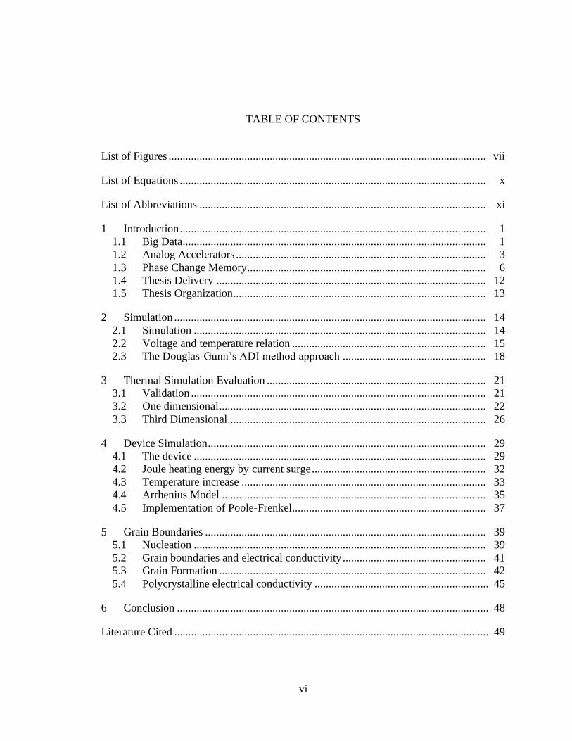
TABLE OF CONTENTS
List of Figures ................................................................................................................. vii
List of Equations ............................................................................................................. x
List of Abbreviations ...................................................................................................... xi
1 Introduction ............................................................................................................. 1 1.1 Big Data............................................................................................................ 1
1.2 Analog Accelerators ......................................................................................... 3
1.3 Phase Change Memory..................................................................................... 6 1.4 Thesis Delivery ................................................................................................ 12 1.5 Thesis Organization.......................................................................................... 13
2 Simulation ............................................................................................................... 14
2.1 Simulation ........................................................................................................ 14
2.2 Voltage and temperature relation ..................................................................... 15 2.3 The Douglas-Gunn’s ADI method approach ................................................... 18
3 Thermal Simulation Evaluation .............................................................................. 21 3.1 Validation ......................................................................................................... 21
3.2 One dimensional ............................................................................................... 22
3.3 Third Dimensional............................................................................................ 26
4 Device Simulation ................................................................................................... 29 4.1 The device ........................................................................................................ 29 4.2 Joule heating energy by current surge .............................................................. 32
4.3 Temperature increase ....................................................................................... 33 4.4 Arrhenius Model .............................................................................................. 35
4.5 Implementation of Poole-Frenkel..................................................................... 37
5 Grain Boundaries .................................................................................................... 39 5.1 Nucleation ........................................................................................................ 39
5.2 Grain boundaries and electrical conductivity ................................................... 41 5.3 Grain Formation ............................................................................................... 42
5.4 Polycrystalline electrical conductivity .............................................................. 45
6 Conclusion ............................................................................................................... 48
Literature Cited ................................................................................................................ 49
vii
LIST OF FIGURES
Fig. 1. Performance against amount data for manual data manipulation, standard
machinelearning, and deep neural networks. [2] ............................................... 1
Fig. 2. Neural networks in A) electrical hardware and B) bio hardware (brain). [4] ... 2
Fig. 3. A) Digital accelerators based on the Von Neumann Architecture (VNA)
and B) the none-VNA analog accelerator. [5] .................................................. 4
Fig. 4. A) Computational graph & B) Hardware implementation of neural
networks.[5][6][7] C) A PCM cell structure representation [8]. ...................... 5
Fig. 5. PCM cross bar devices, beside a projected and mushroom cell with
amorphous plug and crystalline surrounding it. [9] .......................................... 7
Fig. 6. The different states of PCM operation, RESET and SET. Describing the
change in applied voltage against the device current and resistance. [11]
[12] .................................................................................................................... 8
Fig. 7. The nucleation dominated GST, that nucleate from the inside and
outside, with a continuous pulse or step pulses. [13] ........................................ 10
Fig. 8. A) Voltage and B) Temperature presented as third dimensional mesh
resistors. ............................................................................................................ 17
Fig. 9. Steady heat transfer through a slab of material, to be shown that it is
alike a series of electrical resistors.................................................................... 23
Fig. 10. A) Our simulation and B) ANSYS simulation for the structure of 1
dimensional heat transfer. ................................................................................. 24
Fig. 11. The temperature distribution across the one-dimensional structure in the
ANSYS and IBM developed simulations, and the literature value across it. ... 25
Fig. 12. A) A 3D cube with symmetrical C) temperature gradient through its
Z-slice center and C) temperature gradient lining up in all dimensions
from the center. ................................................................................................. 26
Fig. 13. A) Two slices of the third dimensional domain to calculate the thermal
energy output across B) slice faces. .................................................................. 27
viii
Fig. 14. A) The device simulated against the experimental data analysis. B) The
description of electrical current traveling from the top to bottom contact.
C) The impact of melting on electrical current path. ......................................... 29
Fig. 15. A) The electrical conductivity of crystalline and molten GST. B) The
thermal conductivity dependent on the Wiedemann-Franz model. C) The
phase transition of GST and the structural property change, causing a
jump. D) The effect in the IV graph. ................................................................ 31
Fig. 16. A) Current flow and energy generation on top of heater. B) A closer view
of the energy from the side and top. ................................................................. 33
Fig. 17. Temperature 2D slice of simulated device, at different time intervals. ............ 34
Fig. 18. Albany Nanotech Center PCM device mean and median experimental
results (Benedict Kersting IBM Zurich lab) against device simulations at
different activation energies. ............................................................................. 36
Fig. 19. Poole-Frenkel Field effect on electrons by traps, increasing electrical
conductivity by field effect. .............................................................................. 37
Fig. 20. Experimental results with simulation results, using the Poole Frenkel
effect with the Arrhenius model. (Mean and Median PCM experimental
data from Zurich IBM lab 2020, by Benedict Kersting on Albany
Nanotech Center PCM devices) ........................................................................ 38
Fig. 21. The free energy plot of ∆𝐺, showing where the number of monomers
rather reduce than grow, across the critical value nc. [14][19] (Inspiration
from Robin Peter’s presentation) ...................................................................... 40
Fig. 22. A) The crystal structure of crystalline, amorphous, and polycrystalline,
where the pink line indicates a grain boundary. [21] B) Percolation
through a medium with changing resistance. .................................................... 42
Fig. 23. A) A slab of phase change material with an anode and cathode probed.
B) The resulting crystallization over time at a ramp of 0.01C/min.
Showing the grain ids on top and the phase on the bottom. (Crystalline =
yellow, Blue=Amorphous, Dark blue = GB, Brown= Growth front) ............... 43
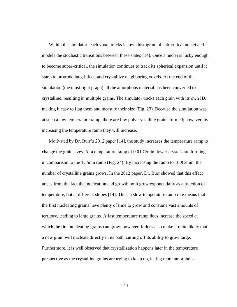
Fig. 24. Crystallization fraction of temperature ramps at 0.01, 1, and 100
C/minute. Determining the temperature ramps effect on the amount of
polycrystalline. .................................................................................................. 45
ix
Fig. 25. A) Polycrystalline cell state B) potential drop, C) electrical conductivity
(top) changes with crystal fraction growth (bottom), and D) current field
map. ................................................................................................................... 46
Fig. 26. Electrical resistance change against crystal fraction growth with different
temperature ramps. ............................................................................................. 47
x
LIST OF EQUATIONS
Equation 1: Joule Heating ........................................................................................... 15
Equation 2: Poisson Equation [16] .............................................................................. 16
Equation 3: A) Kirchhoff’s Current law, B) capacitance and current relation
equation, C) modified Voltage equation. ................................................. 16
Equation 4: A) Cartesian thermal diffusion equation, B) is eq 3 C) ........................... 18
Equation 5: A) The Crank-Nicolson thermal equation [15], B) Voltage in CN
format, derived Crank-Nicolson thermal equation .................................. 18
Equation 6: A) Douglas-Gunn ADI method, B) the three step Douglas-Gunn ADI
method approach [15] .............................................................................. 19
Equation 7: Fourier's heat equation, one dimensional ................................................. 21
Equation 8: Power equation......................................................................................... 22
Equation 9: Electrical conductivity by the Arrhenius model ...................................... 31
Equation 10: Wiedemann-Franz model [17] ................................................................. 32
Equation 11: Implemented Poole-Frenkel into Arrhenius model.................................. 37
Equation 12: Free energy [12] [14] ............................................................................... 39
xi
LIST OF ABBREVIATIONS
ML – Machine Learning
DNN - Deep Neural Networks
PCM – Phase Change Memory
IV – Current vs Voltage
ADI – Alternating Direction Implicit
FDM – Finite Difference Method
FEM – Finite Element Method
TCAD - Technology Computer-Aided Design
RV – resistance voltage
RP – resistance power
1
1 INTRODUCTION
1.1 Big Data
The internet is the global system of interconnected communication between networks
and devices. Today, 5 billion people use the internet; by 2022 that number will be 6
billion, which is more than 20% of the growing global population. [1]
Big data describes the large volume of data on the internet, both structured and
unstructured. However, it is not the amount of data that is important; it is what
organizations do with the data that matters. Big data can be analyzed for insights that lead
to better decisions and strategic business moves. By 2022, the amount of data in the
world is estimated to grow to 175 zettabytes of data, where a zettabyte is 10 to the 21st
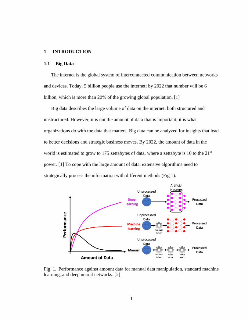
power. [1] To cope with the large amount of data, extensive algorithms need to
strategically process the information with different methods (Fig 1).
Fig. 1. Performance against amount data for manual data manipulation, standard machine
learning, and deep neural networks. [2]
2
An algorithm is a finite sequence of well-defined, computer-implementable
instructions, typically used to solve a class of problems or to perform a computation.
Man-made algorithms can handle moderate amounts of data; however, the performance
of scaling with large amounts of data becomes a hassle, especially when there are many
different types of data (Fig. 1).
Machine learning (ML) uses algorithms to parse data, learn from it, and make
informed decisions based on what it has learned. While it can work well for large
amounts of data, its performance saturates as the amount of data increases (Fig. 1). Its
saturation is due to the need for manual extraction of the features for the algorithms to
learn. [3]
Deep learning (DL), on the other hand, involves artificial neural networks that can
learn and make intelligent decisions on their own (Fig. 1). Instead of needing manual
extractions, the DL does so itself, creating deep artificial neurons that continues to
increase performance with larger amounts of data. [3]
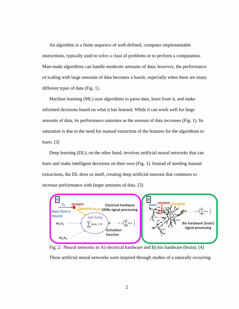
Fig. 2. Neural networks in A) electrical hardware and B) bio hardware (brain). [4]
These artificial neural networks were inspired through studies of a naturally occurring
3
neural network in the human biological hardware: the brain (Fig. 2 B). The brain is made
up of complex parts that contain many billions of neurons. As signals travel from one
axon to a dendrite through a synapse, signals will change dependent on the chemical
ionic composition, creating instances, fantasies, memories, or object identification (Fig.
2). Similar interactions occur within deep neural networks, with signals entering one
layer of neurons leading to a cascade of effects that are triggered in neurons deeper
within the network (Fig. 2 A). While a brain is a biological wetware that works by
biochemistry, a computer implements a deep neural network (DNN) with software
running on electronic hardware, such as digital accelerators, CPUs, or GPUs [5]. These
kinds of hardware are all based on the Von Neumann architecture.
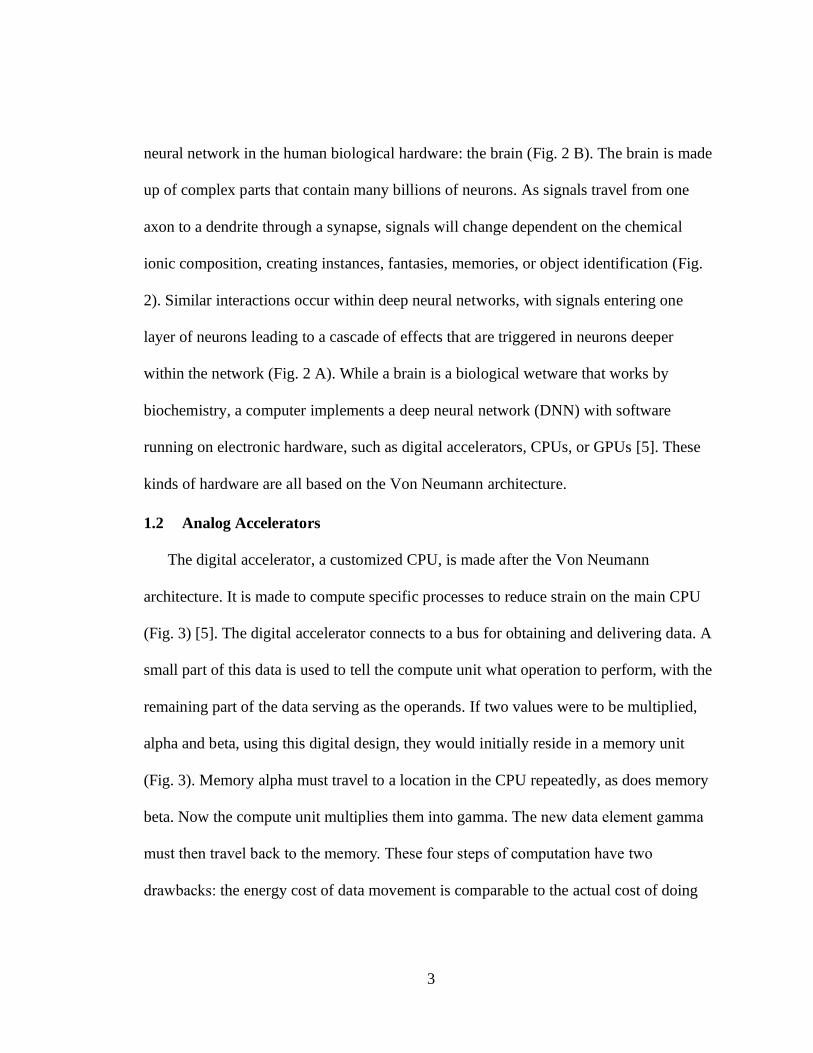
1.2 Analog Accelerators
The digital accelerator, a customized CPU, is made after the Von Neumann
architecture. It is made to compute specific processes to reduce strain on the main CPU
(Fig. 3) [5]. The digital accelerator connects to a bus for obtaining and delivering data. A
small part of this data is used to tell the compute unit what operation to perform, with the
remaining part of the data serving as the operands. If two values were to be multiplied,
alpha and beta, using this digital design, they would initially reside in a memory unit
(Fig. 3). Memory alpha must travel to a location in the CPU repeatedly, as does memory
beta. Now the compute unit multiplies them into gamma. The new data element gamma
must then travel back to the memory. These four steps of computation have two
drawbacks: the energy cost of data movement is comparable to the actual cost of doing
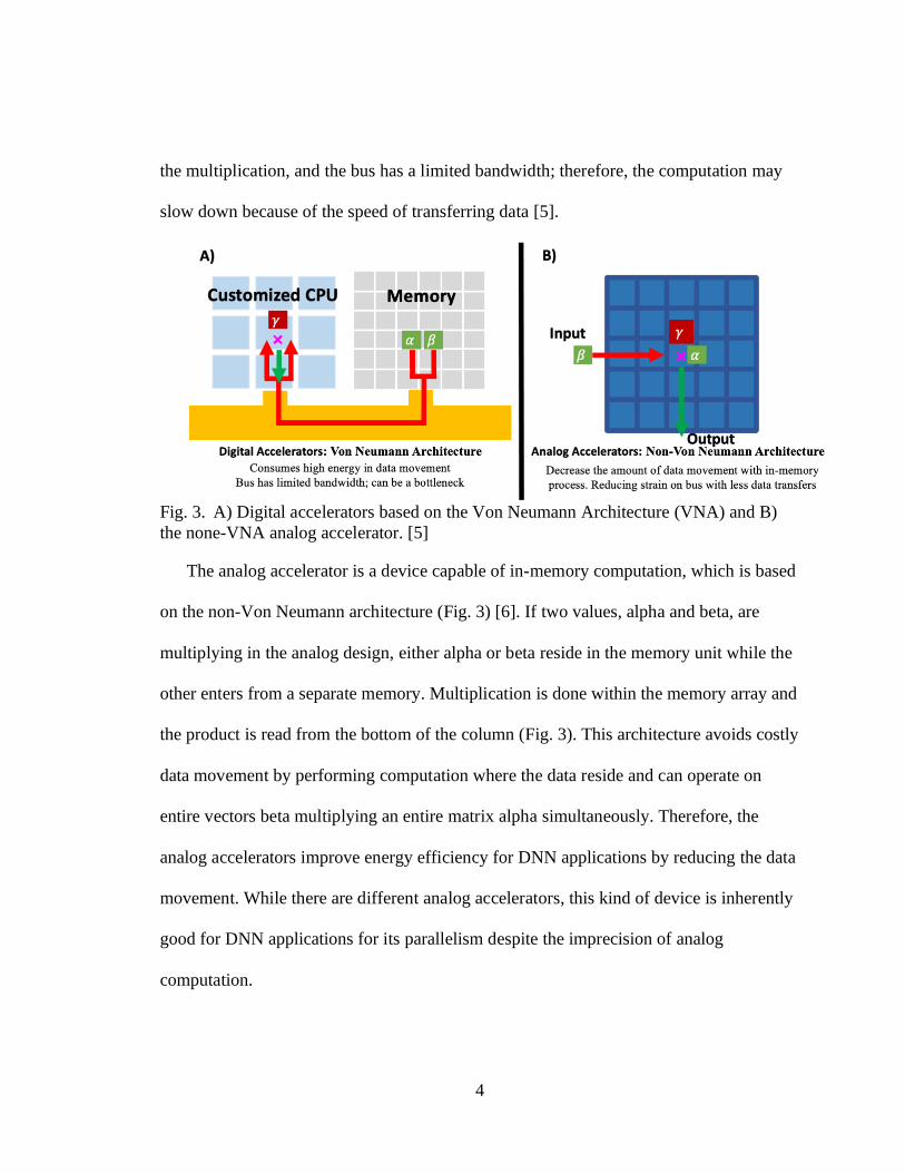
4
the multiplication, and the bus has a limited bandwidth; therefore, the computation may
slow down because of the speed of transferring data [5].
Fig. 3. A) Digital accelerators based on the Von Neumann Architecture (VNA) and B)
the none-VNA analog accelerator. [5]
The analog accelerator is a device capable of in-memory computation, which is based
on the non-Von Neumann architecture (Fig. 3) [6]. If two values, alpha and beta, are
multiplying in the analog design, either alpha or beta reside in the memory unit while the
other enters from a separate memory. Multiplication is done within the memory array and
the product is read from the bottom of the column (Fig. 3). This architecture avoids costly
data movement by performing computation where the data reside and can operate on
entire vectors beta multiplying an entire matrix alpha simultaneously. Therefore, the
analog accelerators improve energy efficiency for DNN applications by reducing the data
movement. While there are different analog accelerators, this kind of device is inherently
good for DNN applications for its parallelism despite the imprecision of analog
computation.
5
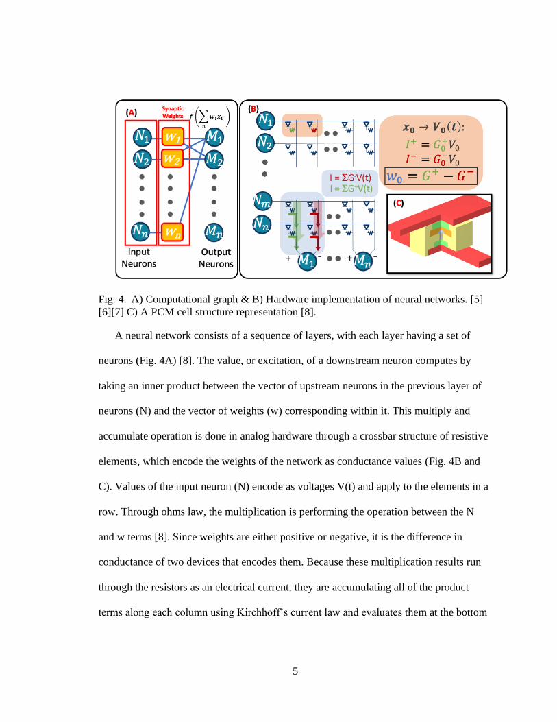
Fig. 4. A) Computational graph & B) Hardware implementation of neural networks. [5]
[6][7] C) A PCM cell structure representation [8].
A neural network consists of a sequence of layers, with each layer having a set of
neurons (Fig. 4A) [8]. The value, or excitation, of a downstream neuron computes by
taking an inner product between the vector of upstream neurons in the previous layer of
neurons (N) and the vector of weights (w) corresponding within it. This multiply and
accumulate operation is done in analog hardware through a crossbar structure of resistive
elements, which encode the weights of the network as conductance values (Fig. 4B and
C). Values of the input neuron (N) encode as voltages V(t) and apply to the elements in a
row. Through ohms law, the multiplication is performing the operation between the N
and w terms [8]. Since weights are either positive or negative, it is the difference in
conductance of two devices that encodes them. Because these multiplication results run
through the resistors as an electrical current, they are accumulating all of the product
terms along each column using Kirchhoff’s current law and evaluates them at the bottom
6
of the array (Fig. 4 B). Thereafter, a nonlinearity function, f(x), squashes the result to
produce the output neuron M. Each layer of the network continues to perform the
multiply and accumulate operation.
One resistive element that can act as the weight is the phase-change memory (PCM)
(Fig. 4C). The PCM unit cell is an electrically tunable resistor, which acts as the
manipulating resistance variable. Because these analog accelerators depend on the precise
manipulation of the variable resistance unit at each node of the crossbar array, it is crucial
to understand and accurately model the underlying physics. Therefore, the electrically
tunable resistors in the DNN crossbar array motivates to simulate the PCM device and its
operations.
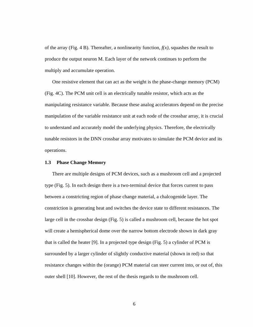
1.3 Phase Change Memory
There are multiple designs of PCM devices, such as a mushroom cell and a projected
type (Fig. 5). In each design there is a two-terminal device that forces current to pass
between a constricting region of phase change material, a chalcogenide layer. The
constriction is generating heat and switches the device state to different resistances. The
large cell in the crossbar design (Fig. 5) is called a mushroom cell, because the hot spot
will create a hemispherical dome over the narrow bottom electrode shown in dark gray
that is called the heater [9]. In a projected type design (Fig. 5) a cylinder of PCM is
surrounded by a larger cylinder of slightly conductive material (shown in red) so that
resistance changes within the (orange) PCM material can steer current into, or out of, this
outer shell [10]. However, the rest of the thesis regards to the mushroom cell.
7
Fig. 5. PCM cross bar devices, beside a projected and mushroom cell with amorphous
plug and crystalline surrounding it. [9]
As a current is conducted through the mushroom cell from the top to the bottom
electrode, this chalcogenide layer gets hot and can change states, switching between a
disorganized amorphous phase that has high resistivity and an ordered crystalline phase
that has low resistivity. These changing local properties cause the device to switch weight
in the neuron layers. When used as a binary memory device, the low resistance state is
called the set state, and the process of switching into the high resistance state is called the
reset operation.
Starting in set state, a mushroom cell full of crystalline material (Fig. 6 Set state) is a
highly conductive material. If a small read voltage passes through it, small enough to not
disturb the material state and measure the current out, it shows a low resistance
8
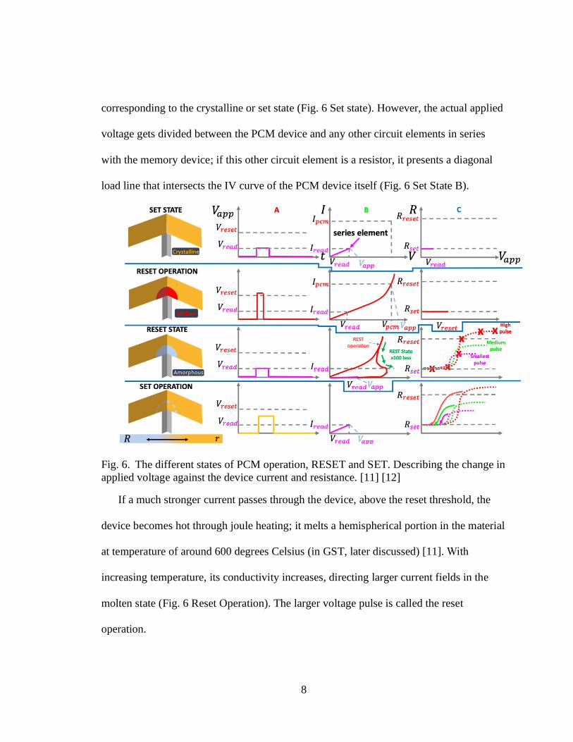
corresponding to the crystalline or set state (Fig. 6 Set state). However, the actual applied
voltage gets divided between the PCM device and any other circuit elements in series
with the memory device; if this other circuit element is a resistor, it presents a diagonal
load line that intersects the IV curve of the PCM device itself (Fig. 6 Set State B).
Fig. 6. The different states of PCM operation, RESET and SET. Describing the change in
applied voltage against the device current and resistance. [11] [12]
If a much stronger current passes through the device, above the reset threshold, the
device becomes hot through joule heating; it melts a hemispherical portion in the material
at temperature of around 600 degrees Celsius (in GST, later discussed) [11]. With
increasing temperature, its conductivity increases, directing larger current fields in the
molten state (Fig. 6 Reset Operation). The larger voltage pulse is called the reset
operation.
9
As the electrical pulse stops, the cooling process starts quickly and rapidly because
the device is small. If the material is brought out of the liquid state and down to room
temperature fast enough, without giving time for crystallization to occur, it has
successfully quenched the device. This results in an amorphous plug in the material, right
at the top of the narrow heater electrode, which causes the resulting device resistance to
increase (Fig. 6 Reset State). A PCM device can easily exhibit 100x or larger resistance
ratio between the set and reset states. However, since current is the dependent factor, the
resistance depends on electrical pulse length, electrical intensity, or heater size (Fig. 6
Reset State C). If there are devices with different heater diameters, there are changes in
both the voltage at which the reset transition occurred and the differences in the
maximum total resistance. This is undesirable because it means that it is important to
fabricate every device to have the same heater size. However, it turns out each of these
devices can be brought to intermediate resistance states between the full set and reset
states. This creates great opportunity to store the analog conductance needed for the
accelerators. However, the importance of understanding variability and understanding
how to get devices to precisely land in the intermediate resistance states additionally
motivates the interest in modeling PCM devices.
10
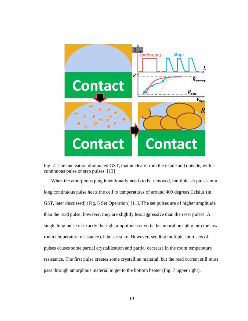
Fig. 7. The nucleation dominated GST, that nucleate from the inside and outside, with a
continuous pulse or step pulses. [13]
When the amorphous plug intentionally needs to be removed, multiple set pulses or a
long continuous pulse heats the cell to temperatures of around 400 degrees Celsius (in
GST, later discussed) (Fig. 6 Set Operation) [11]. The set pulses are of higher amplitude
than the read pulse; however, they are slightly less aggressive than the reset pulses. A
single long pulse of exactly the right amplitude converts the amorphous plug into the low
room temperature resistance of the set state. However, sending multiple short sets of
pulses causes some partial crystallization and partial decrease in the room temperature
resistance. The first pulse creates some crystalline material, but the read current still must
pass through amorphous material to get to the bottom heater (Fig. 7 upper right).
11
However, by continuing to send pulses they can create an all-crystalline pathway for the
read current.
The most popular phase-change material is called GST, Germanium Antimony
Tellurium. It is what’s called a nucleation dominated material [13]. This means that there
are two ways to remove the amorphous plug. As the plug nucleates new crystalline
nuclei, it can have crystal clusters reappear from the inside and there can be regrowth
from the crystalline material surrounding the plug. By applying a large pulse to the
material, the electrical conductivity will be lowered quickly due to the nucleation
domination. However, while sending the electrical set pulses through the GST after a
large pulse, the device resistance can continue to decrease. Therefore, the nucleation
domination creates something that is still changing as more pulses are fired (G. Burr,
personal communication, January 20, 2020).
As the amorphous plug changes to crystalline, grains are popping up like popcorn
depending on which random nuclei gained enough energy to be stable, and then could
grow larger and consume its amorphous surroundings (Fig. 7). At the point when a
crystalline path has been made through the amorphous material, the plug may already be
mostly in the crystalline phase (shown in orange), but between the grains there are still
amorphous like grain boundaries (shown in brown). This is now in a polycrystalline
phase. Now the device continues to decrease in electrical resistance due to the heat
generation as multiple pulses are applied. A hypothesis to explain this is that the heat is
reducing the number of grains, as big grains consume and eliminate small ones [14]. This
12
means that the electrical read current must pass through fewer grain boundaries to get to
the bottom electrode. To add to the hypothesis, this grain growth is what explains the
continual changes in device resistance. This means that there is a strong incentive to
include the creation and influence of grains and grain boundaries on the read current in a
TCAD simulator for studying the switching physics of these devices, particularly if there
are interests in the intermediate resistance states.
1.4 Thesis Delivery
IBM has long been at the forefront of PCM device technology, initially driven
by storage class memories and other data-storage applications. As part of this work, IBM
built a full 3D simulation modeling tool. This simulator uses the finite difference method
to approximate the derivatives within the underlying differential equations being
simulated. Thermodynamic modeling was enabled by the alternating direction implicit
(ADI) method, which divides each timestep into three parts, one part for each Cartesian
direction [15]. This allows a tri-diagonal-matrix approach, which can solve systems of
implicit equations in 1D, to be extended to three dimensions. This tool can also simulate
the nucleation and growth of polycrystalline grains [14]; however, it currently lacks the
capability of modeling the subsequent interaction of grains, the motion of grain
boundaries, or the full electrical impact of these grain boundaries. Although the local
IBM team later moved to analog-AI architectures, successfully publishing their work
based on PCM devices in Nature [7]. The existing TCAD simulator has not been
incorporated into any analog-AI work to date.
13
Therefore, to further develop the model and extend it for the investigation of
intermediate resistance states applicable to Analog AI, the purpose of this thesis is to
verify and validate the simulator, study its ability to track device simulations, and study
grain boundary impact on electrical conductivity. The study is done against literature
models and experimental results regarding to thermodynamics in PCM. The expected
outcome of this study was to validate and improve a tool that can be used across IBM
Research for engineering of the future analog-AI and memory systems based on PCM
technology.
1.5 Thesis Organization
The f thesis is organized in 6 chapters:
• Chapter 1: Includes the background information of PCM and the reason for the thesis.
• Chapter 2: Includes the explanation of the method used to simulate thermodynamic and
voltage distribution using the ADI method.
• Chapter 3: Includes the accuracy of the thermal modeling, comparing a one-dimensional
simulation against the industrial software ANSYS, while showing thermal distribution in
all directions and accuracy of the conservation of energy.
• Chapter 4: Simulates PCM against experimental data and adds standard physics for
improving the TCAD software.
• Chapter 5: Studies the grain boundary growth effect on electrical conductivity, due to
the formation of grains at different temperature ramping within GST.
• Chapter 6: Concludes the thesis.
14
2 SIMULATION
The simulator was created in 2004 at IBM’s Almaden Research Center by Dr.
Geoffrey Burr and has since been updated in 2012 and 2018 [14]. Its purpose is to
simulate the PCM devices within the third dimensional domain using the finite difference
method (FDM) and the Douglas-Gunn approach of the alternating direction implicit
(ADI) method. The chapter will describe the ADI methods approach to calculate both
voltage and temperature distribution that are the main factors for material changes.
2.1 Simulation
The most common method in industrial semiconductor simulating tools is the finite
element method (FEM). The FEM requires a significant amount of computer power, but
it can simulate fine structures through its triangular mesh. FDM, on the other hand, does
not need as much power for simple structures and reduces the number of needed nodes.
However, FDM’s rectangular mesh requires a larger number of nodes to simulate fine
structures. Because typical bar structures of PCM mushroom cells can be ideal
rectangular shapes, the FDM approach is a better candidate due to quick and accurate
simulations.
A conventional semiconductor simulator would track full electrical effects, including
drift diffusion and the dopant concentration within materials. However, this simulator
uses a third dimensional mesh of voxelated resistors, driving the simulation to completion
by minimizing leakage error current. The electrical, thermal, and nucleation models are
15
each updated once per cycle and provide the necessary information for computation of
the subsequent components.
The simulator initializes by applying a set voltage. It does so through evaluating
Poisson’s equation from an initialized voxel mesh. Thereafter, the mesh’s electrical field
and current density response is used to compute joule heating, which is heat generation
from electrical energy (Equation 1). However, thermal sources from no joule heating are
also possible through selected thermal generators.
Equation 1: Joule Heating
𝑄𝑣(𝑥, 𝑡) = 𝐽2(𝑥, 𝑡)
𝜎
Thereafter, the simulator uses the Douglas-Gunn’s approach to find the temperature
distribution from the generating heat source of either joule heating or others. Because it
knows the temperature, the simulator detects if a phase change material at each voxel is
crystallized, amorphized by quenching, or liquified through melting, which provides
resistance information for the next cycle to evaluate the current density. From here, the
cycle repeats until a termination state is reached, which is a pre-determined duration, a
maximum temperature, or a crystallization fraction.
2.2 Voltage and temperature relation
While voltage and temperature are two different phenomena, they are both dependent
on similar variables and equations. The third dimensional Poisson equation (Equation 2)
is used to calculate the voltage distribution in a Cartesian coordinated system. The first
16
value is negative charge over the material permittivity, which is equated to the sum of the
second spatial derivative of voltage in all coordinate directions. However, within the
simulator, there is no charge generation, and therefore, this term is equal to 0. The sum of
the voltage differentials must now be equal to 0.
Equation 2: Poisson Equation [16]
𝜌
𝜖𝑜= ∆𝑉 = 𝛻2𝑉 = (
𝛿2
𝛿𝑥2+
𝛿2
𝛿𝑦2+
𝛿2
𝛿𝑧2) 𝑉
−𝜌(𝑥, 𝑦, 𝑧)
∈𝑜=
𝛿2𝑉(𝑥, 𝑦, 𝑧)
𝛿𝑥2+
𝛿2𝑉(𝑥, 𝑦, 𝑧)
𝛿𝑦2+
𝛿2𝑉(𝑥, 𝑦, 𝑧)
𝛿𝑧2
0 =𝛿2𝑉(𝑥, 𝑦, 𝑧)
𝛿𝑥2+
𝛿2𝑉(𝑥, 𝑦, 𝑧)
𝛿𝑦2+
𝛿2𝑉(𝑥, 𝑦, 𝑧)
𝛿𝑧2
Equation 3: A) Kirchhoff’s Current law, B) capacitance and current relation equation, C)
modified Voltage equation.
A) 0 = 𝐼𝑥−/+ + 𝐼𝑦−/+ + 𝐼𝑧−/+
B) 𝐶𝛿𝑉
𝛿𝑡= 𝐼 =
𝑉
𝑅 𝐶
𝛿𝑉(𝑥, 𝑦, 𝑧)
𝛿𝑡=
𝑉(𝑥, 𝑦, 𝑧)
𝑅≈
𝛻2𝑉
𝑅
C) 𝐶𝛿𝑉(𝑥, 𝑦, 𝑧)
𝛿𝑡=
1
𝑅𝑥
𝛿2𝑉(𝑥, 𝑦, 𝑧)
𝛿𝑥2+
1
𝑅𝑦
𝛿2𝑉(𝑥, 𝑦, 𝑧)
𝛿𝑦2+
1
𝑅𝑧
𝛿2𝑉(𝑥, 𝑦, 𝑧)
𝛿𝑧2
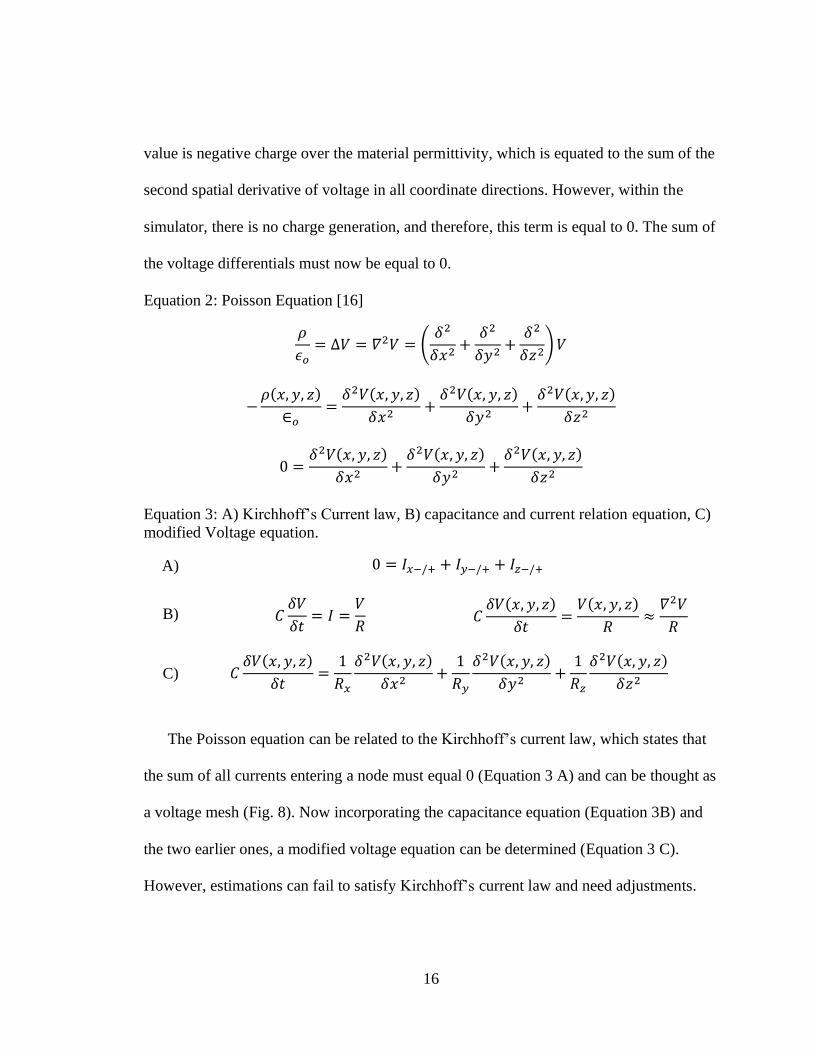
The Poisson equation can be related to the Kirchhoff’s current law, which states that
the sum of all currents entering a node must equal 0 (Equation 3 A) and can be thought as
a voltage mesh (Fig. 8). Now incorporating the capacitance equation (Equation 3B) and
the two earlier ones, a modified voltage equation can be determined (Equation 3 C).
However, estimations can fail to satisfy Kirchhoff’s current law and need adjustments.
17
Through implementing an imaginary capacitor to each node, any current that fails to
satisfy the Kirchhoff’s current law in the resistors must pass through the capacitor into
the ground. Therefore, the capacitance can act as a fudge factor so that the simulator can
converge the electrical voltage distribution. However, what is important to understand is
that every time it is run, steady state must be reached. If the equation stops before the
system has converged at steady state, there is potentially a large error current and
significant deviations from Poisson’s equation.
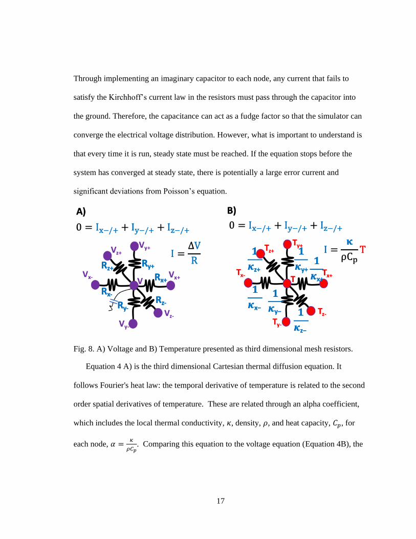
Fig. 8. A) Voltage and B) Temperature presented as third dimensional mesh resistors.
Equation 4 A) is the third dimensional Cartesian thermal diffusion equation. It
follows Fourier's heat law: the temporal derivative of temperature is related to the second
order spatial derivatives of temperature. These are related through an alpha coefficient,
which includes the local thermal conductivity, 𝜅, density, 𝜌, and heat capacity, 𝐶𝑝, for
each node, 𝛼 =𝜅
𝜌𝐶𝑝. Comparing this equation to the voltage equation (Equation 4B), the
18
heat can be thought of in terms of Kirchhoff’s current law, which relates this variable
alpha as if it was a kind of electrical conductance (Fig. 8). By looking at both the voltage
and temperature equation, there is a same first derivative in time on the left-hand side and
the same second-derivatives in space on the righthand side (Fig 8. A & B). However,
while the voltage equation is driven to steady state, the temperature equation uses the
actual physical timestep itself and computes the small temperature changes within any
given simulation cycle.
Equation 4: A) Cartesian thermal diffusion equation, B) is eq 3 C)
A) 𝜕𝑇(𝑥, 𝑦, 𝑧)
𝜕𝑡= 𝛼 [
𝜕𝑥2𝑇(𝑥, 𝑦, 𝑧)
𝜕𝑥2+
𝜕𝑦2𝑇(𝑥, 𝑦, 𝑧)
𝜕𝑦2+
𝜕𝑧2𝑇(𝑥, 𝑦, 𝑧)
𝜕𝑧2] +
1
𝜌𝐶𝑝𝑔(𝑥, 𝑦, 𝑧)
B) 𝐶𝛿𝑉(𝑥, 𝑦, 𝑧)
𝛿𝑡=
1
𝑅𝑥
𝛿2𝑉(𝑥, 𝑦, 𝑧)
𝛿𝑥2+
1
𝑅𝑦
𝛿2𝑉(𝑥, 𝑦, 𝑧)
𝛿𝑦2+
1
𝑅𝑧
𝛿2𝑉(𝑥, 𝑦, 𝑧)
𝛿𝑧2
2.3 The Douglas-Gunn’s ADI method approach
The Crank-Nicolson thermal equation is a 1 to 1 unconditionally stable equation that
is derived from the explicit and the implicit thermal equation (Equation 5 A) [15].
Equation 5: A) The Crank-Nicolson thermal equation [15], B) Voltage in CN format,
derived Crank-Nicolson thermal equation
A) 𝑇𝑛+1+𝑇𝑛
∆𝑡= 𝛼 [
𝜕𝑥2𝑇𝑛+1+𝜕𝑥
2𝑇𝑛
2(∆𝑥)2 +𝜕𝑦
2𝑇𝑛+1+𝜕𝑦2𝑇𝑛
2(∆𝑦)2 +𝜕𝑧
2𝑇𝑛+1+𝜕𝑧2𝑇𝑛
2(∆𝑧)2 ] +1
𝜌𝐶𝑝𝑔(𝑥, 𝑦, 𝑧)
B) 𝐶𝑉𝑛+1+𝑉𝑛
∆𝑡= [
1
𝑅𝑥
𝜕𝑥2𝑉𝑛+1+𝜕𝑥
2𝑉𝑛
2(∆𝑥)2 +1
𝑅𝑦
𝜕𝑦2𝑉𝑛+1+𝜕𝑦
2𝑉𝑛
2(∆𝑦)2 +1
𝑅𝑧
𝜕𝑧2𝑉𝑛+1+𝜕𝑧
2𝑉𝑛
2(∆𝑧)2 ] []
C)
−𝑟𝑥𝑇𝑥−1,𝑦,𝑧𝑛+1 − 𝑟𝑦𝑇𝑥,𝑦−1,𝑧
𝑛+1 − 𝑟𝑧𝑇𝑥,𝑦,𝑧−1𝑛+1 + 2(1 + 𝑟𝑥 + 𝑟𝑦 + 𝑟𝑧)𝑇𝑥,𝑦,𝑧
𝑛+1 − 𝑟𝑥𝑇𝑥+1,𝑦,𝑧𝑛+1
− 𝑟𝑥𝑇𝑥,𝑦+1,𝑧𝑛+1 − 𝑟𝑥𝑇𝑥,𝑦,𝑧+1
𝑛+1
19
= 𝑟𝑥𝑇𝑥−1,𝑦,𝑧𝑛 + 𝑟𝑦𝑇𝑥,𝑦−1,𝑧
𝑛+1 + 𝑟𝑧𝑇𝑥,𝑦,𝑧−1𝑛+1 + 2(1 − 𝑟𝑥 − 𝑟𝑦 − 𝑟𝑧)𝑇𝑥,𝑦,𝑧
𝑛 + 𝑟𝑥𝑇𝑥+1,𝑦,𝑧𝑛+1
+ 𝑟𝑥𝑇𝑥,𝑦+1,𝑧𝑛+1 + 𝑟𝑥𝑇𝑥,𝑦,𝑧+1
𝑛+1 +2∆𝑡
𝜌𝐶𝑝𝑔𝑥,𝑦,𝑧
The formula calculates the Cartesian thermal diffusion equation. Because equation 4A
and 4B are alike, the same can be done with the Crank-Nicolson to the voltage equation
(Equation 5 B). However, the Crank-Nicolson equation is complicated, and when
simplified it generates a large equation with up to 7 unknown values for the next time
step (Equation 5 C). Instead, Douglas and Gunn derived from the Crank-Nicholson
equation using the ADI method to make a new simpler equation that is third
dimensionally first ordered accurate [15].
Equation 6: A) Douglas-Gunn ADI method, B) the three step Douglas-Gunn ADI method
approach [15]
A)
𝑇𝑛+1 − 𝑇𝑛 = 𝑟𝑥
𝜕𝑥2
2(𝑇𝑛+1 − 𝑇𝑛) + 𝑟𝑦
𝜕𝑦2
2(𝑇𝑛+1 − 𝑇𝑛)
+ 𝑟𝑧
𝜕𝑧2
2(𝑇𝑛+1 − 𝑇𝑛) +
∆𝑡
𝜌𝐶𝑝𝑔
𝑟𝑥,𝑦,𝑧 =𝛼∆𝑡
(𝛿𝑥, 𝑦, 𝑧)2
B)
𝑇𝑛+13 − 𝑇𝑛 =
𝑟𝑥𝜕𝑥2
2(𝑇𝑛+
13 + 𝑇𝑛) + 𝑟𝑦𝜕𝑥
2𝑇𝑛 + 𝑟𝑧𝜕𝑧2𝑇𝑛 +
∆𝑡
𝜌𝐶𝑝𝑔
𝑇𝑛+23 − 𝑇𝑛 =
𝑟𝑥𝜕𝑥2
2(𝑇𝑛+
13 + 𝑇𝑛) +
𝑟𝑦𝜕𝑥2
2(𝑇𝑛+
23 + 𝑇𝑛) + 𝑟𝑧𝜕𝑧
2𝑇𝑛 +∆𝑡
𝜌𝐶𝑝𝑔
𝑇𝑛+1 − 𝑇𝑛 =𝑟𝑥𝜕𝑥
2
2(𝑇𝑛+
1
3 + 𝑇𝑛) +𝑟𝑦𝜕𝑥
2
2(𝑇𝑛+
2
3 + 𝑇𝑛) +𝑟𝑧𝜕𝑧
2
2(𝑇𝑛+1 + 𝑇𝑛) +
∆𝑡
𝜌𝐶𝑝𝑔 [15]
This is the Douglas-Gunn ADI method (Equation 6 A), and it is divided into three
steps for the different coordinates: x, y, and z. The first step is implicit along x and solves
20
for temperatures using 1/3 of the actual full-time step (Equation 6 B). By being explicit
along only one dimension, the tri-diagonal matrix method is used to solve this system of
equations together with appropriate boundary conditions at the simulation boundaries.
The second step is implicit along y and produces the temperatures at t + 2/3, using both
the original temperatures at time t and the results of the first step (Equation 6 B). Finally,
the third timestep generates the temperature at timestep t + 1 (Equation 6 B). This is all
repeated but for the voltage diffusion equation, to calculate it in third dimensional
domains with a first order accuracy.
21
3 THERMAL SIMULATION EVALUATION
The following chapter validates the thermal accuracy of the TCAD simulator. Its
thermal abilities are determined through measuring the steady-heat transfer against a
literature calculation and a ANSYS steady heat transfer simulation, and third dimensional
transfer of thermal energy throughout the device to equal the applied power input.
3.1 Validation
Steady heat state is the transfer of energy with no time change or generation of heat.
In a one-dimensional system, Fourier’s heat diffusion law can compute the steady state of
heat by incorporating dependence on heat conductivity, temperature difference, and the
distance between two points (Equation 7). Fourier’s law of heat transfer is the negative
gradient of temperature and the area across a distance where heat flows. The equation
represents the heat flow, q [𝑊
𝑚2], the material heat conductivity, k [𝑊
𝑚𝐾], the temperature
difference, dT [K], and the distance, dx [m].
Equation 7: Fourier's heat equation, one dimensional
q = −kdT
dx
In third dimensional systems, there are no equations as simple as equation 7.
Therefore, the Crank-Nicolson’s or other mathematical approaches need to be considered,
to estimate the third dimensional heat distribution by simulation. However, all
thermodynamic systems need to follow the law of conservation. The amount of energy
22
that enters a system must leave it. The total injection must be summed through
calculation of joule heating or its direct energy injection of each node in the simulation.
By determining the heat flow across six faces of a cube inside the edge of the simulation,
the power out can be calculated through simple Fourier’s law and compared to the
injected energy (Equation 8). Where Pin is the power input [W], qx+ [𝑊
𝑑𝑦𝑑𝑥] represents the
heat flux in the coordinate direction x+, while dy and dz makes up the area, where the five
other faces are represented by their direction.
Equation 8: Power equation
Pin = ∫ qx+dydz + 5 other faces = Pout
3.2 One dimensional
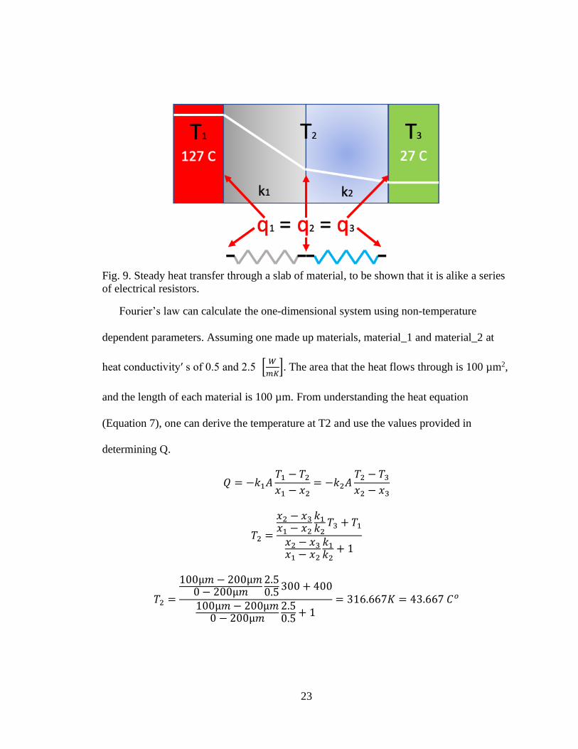
At steady state, the temperature difference driving heat conduction is constant.
Because there are no temperature changes, all the heat transferring in one direction
should be equal (for 1D) if it is from the same source and nothing is interfering.
Therefore, heat transfer through a slab of material can be thought as resistors in contact to
each node. At the equilibration time these heat resistors are constant. A structure of
multiple materials in series can then be thought of as multiple resistors in series (Fig. 9).
The slab has a high temperature potential of T1 of 127 oC and a lower at T3 of 27 oC.
Because materials can be thought of as resistors in series, all heat transfer from T1 to T3
must be equal. It can be seen in the resistor representation that all qs’; q1, q2, and q3 are
all equal while travelling through the structure.
23
Fig. 9. Steady heat transfer through a slab of material, to be shown that it is alike a series
of electrical resistors.
Fourier’s law can calculate the one-dimensional system using non-temperature
dependent parameters. Assuming one made up materials, material_1 and material_2 at
heat conductivity′ s of 0.5 and 2.5 [𝑊
𝑚𝐾]. The area that the heat flows through is 100 µm2,
and the length of each material is 100 µm. From understanding the heat equation
(Equation 7), one can derive the temperature at T2 and use the values provided in
determining Q.
𝑄 = −𝑘1𝐴𝑇1 − 𝑇2
𝑥1 − 𝑥2= −𝑘2𝐴
𝑇2 − 𝑇3
𝑥2 − 𝑥3
𝑇2 =
𝑥2 − 𝑥3𝑥1 − 𝑥2
𝑘1
𝑘2𝑇3 + 𝑇1
𝑥2 − 𝑥3𝑥1 − 𝑥2
𝑘1
𝑘2+ 1
𝑇2 =
100µ𝑚 − 200µ𝑚0 − 200µ𝑚
2.50.5
300 + 400
100µ𝑚 − 200µ𝑚0 − 200µ𝑚
2.50.5
+ 1= 316.667𝐾 = 43.667 𝐶𝑜
24
𝑄 = −0.5 [𝑊
𝑚𝐾] [100 ∗ 100 ∗ µ𝑚2] [
400 − 316.667
0 − 100µ𝑚] = 0.004167𝑊
𝑞 = 416677𝑊
𝑚2
Concluding that the literature temperature at position 2 is 43.67 oC, the total heat flow is
0.004167W, and the flux is 416677[𝑊
𝑚2].
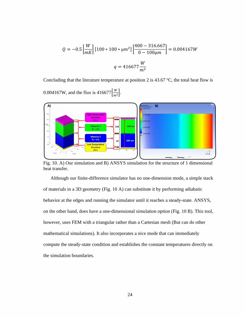
Fig. 10. A) Our simulation and B) ANSYS simulation for the structure of 1 dimensional
heat transfer.
Although our finite-difference simulator has no one-dimension mode, a simple stack
of materials in a 3D geometry (Fig. 10 A) can substitute it by performing adiabatic
behavior at the edges and running the simulator until it reaches a steady-state. ANSYS,
on the other hand, does have a one-dimensional simulation option (Fig. 10 B). This tool,
however, uses FEM with a triangular rather than a Cartesian mesh (But can do other
mathematical simulations). It also incorporates a nice mode that can immediately
compute the steady-state condition and establishes the constant temperatures directly on
the simulation boundaries.
25
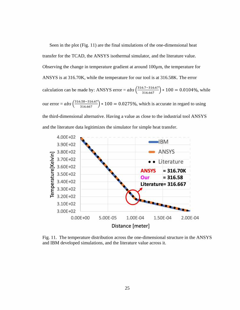
Seen in the plot (Fig. 11) are the final simulations of the one-dimensional heat
transfer for the TCAD, the ANSYS isothermal simulator, and the literature value.
Observing the change in temperature gradient at around 100µm, the temperature for
ANSYS is at 316.70K, while the temperature for our tool is at 316.58K. The error
calculation can be made by: ANSYS error = 𝑎𝑏𝑠 (316.7−316.67
316.667) ∗ 100 = 0.0104%, while
our error = 𝑎𝑏𝑠 (316.58−316.67
316.667) ∗ 100 = 0.0275%, which is accurate in regard to using
the third-dimensional alternative. Having a value as close to the industrial tool ANSYS
and the literature data legitimizes the simulator for simple heat transfer.
Fig. 11. The temperature distribution across the one-dimensional structure in the ANSYS
and IBM developed simulations, and the literature value across it.
26
3.3 Third Dimensional
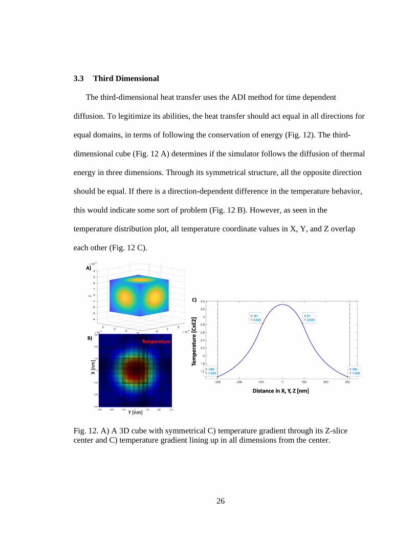
The third-dimensional heat transfer uses the ADI method for time dependent
diffusion. To legitimize its abilities, the heat transfer should act equal in all directions for
equal domains, in terms of following the conservation of energy (Fig. 12). The third-
dimensional cube (Fig. 12 A) determines if the simulator follows the diffusion of thermal
energy in three dimensions. Through its symmetrical structure, all the opposite direction
should be equal. If there is a direction-dependent difference in the temperature behavior,
this would indicate some sort of problem (Fig. 12 B). However, as seen in the
temperature distribution plot, all temperature coordinate values in X, Y, and Z overlap
each other (Fig. 12 C).
Fig. 12. A) A 3D cube with symmetrical C) temperature gradient through its Z-slice
center and C) temperature gradient lining up in all dimensions from the center.
27
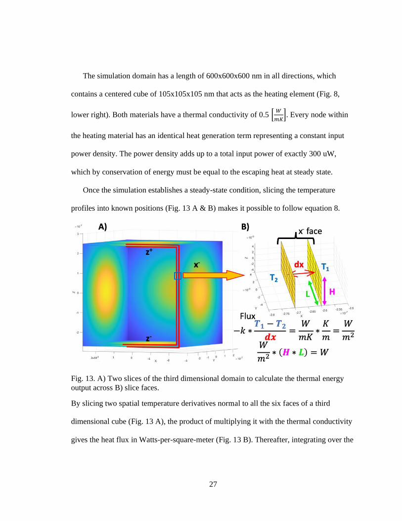
The simulation domain has a length of 600x600x600 nm in all directions, which
contains a centered cube of 105x105x105 nm that acts as the heating element (Fig. 8,
lower right). Both materials have a thermal conductivity of 0.5 [𝑊
𝑚𝐾]. Every node within
the heating material has an identical heat generation term representing a constant input
power density. The power density adds up to a total input power of exactly 300 uW,
which by conservation of energy must be equal to the escaping heat at steady state.
Once the simulation establishes a steady-state condition, slicing the temperature
profiles into known positions (Fig. 13 A & B) makes it possible to follow equation 8.
Fig. 13. A) Two slices of the third dimensional domain to calculate the thermal energy
output across B) slice faces.
By slicing two spatial temperature derivatives normal to all the six faces of a third
dimensional cube (Fig. 13 A), the product of multiplying it with the thermal conductivity
gives the heat flux in Watts-per-square-meter (Fig. 13 B). Thereafter, integrating over the
28
area of the six faces of the cube gives the power in units of Watts. The resulting value is
299.6567 uW, which has a difference of 𝑎𝑏𝑠 (299.6567−300
300) ∗ 100 = 0.1144 %, and
shows that the simulator is closely following the conservation of energy, validating its
third-dimensional usage, and is therefore capable of simulating temperature distributions
for PCM.
29
4 DEVICE SIMULATION
Running laboratory experiments can be expensive and time consuming. Simulating
these experiments numerically can help to reduce the cost of laboratory experiments,
study the detailed physical behavior of PCM, predict the device problems and solutions,
and most importantly develop design intuition that can invent new types of PCM cells.
Therefore, the following chapter simulates the reset procedure of PCM and fits it against
experimental data.
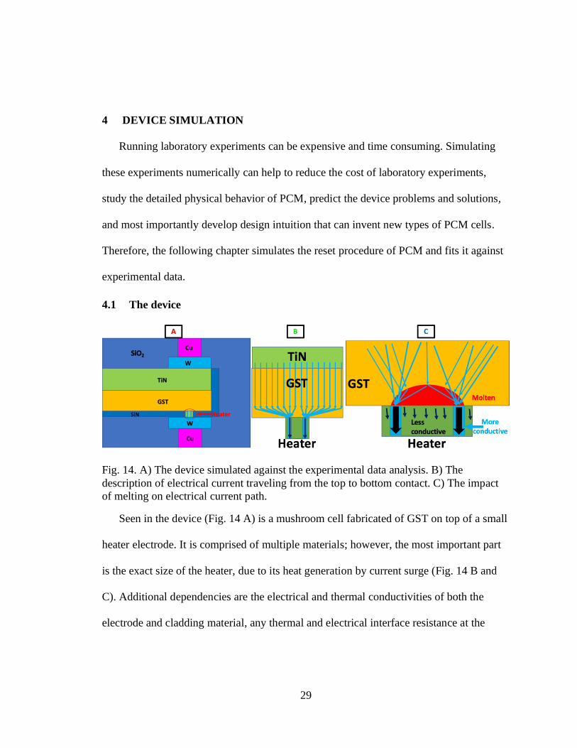
4.1 The device
Fig. 14. A) The device simulated against the experimental data analysis. B) The
description of electrical current traveling from the top to bottom contact. C) The impact
of melting on electrical current path.
Seen in the device (Fig. 14 A) is a mushroom cell fabricated of GST on top of a small
heater electrode. It is comprised of multiple materials; however, the most important part
is the exact size of the heater, due to its heat generation by current surge (Fig. 14 B and
C). Additional dependencies are the electrical and thermal conductivities of both the
electrode and cladding material, any thermal and electrical interface resistance at the
30
material boundaries, the voltage pulse inputs, and its interaction with the rest of the
electrical circuit outside the PCM device. However, because the materials are dependent
on temperature, it is the heater that makes the PCM work.
The heater is the spot where constricting current flows from the top of the electrode to
the bottom or vice-versa depending on the voltage polarity. The arrows (Fig. 14 B) show
the increase in current density entering the heater. To create this current surge, the heater
uses more conductive material (Fig. 14 B and C) (in light blue) in one portion of the
heater with surrounding material (light green) that is more resistive, confining the
current’s path even more. For faster simulations of the material, everything else is a true
insulator and thus blocks all current. This light blue cylindrical shell is where most of the
current flows, which leads to most of the joule heating either in this shell or just above it,
as the current bunches up before leaving the GST material. The heat injection by this
joule heating, and heat loss in all directions away from the body of the GST material,
causes a hemisphere of high temperature centered over the heater. As a result, this is the
region that will be the first to melt (Fig. 14 C).
Current surge is dependent on the electrical conductivity of the device material and is
calculated through the Arrhenius model (Equation 9). Seen in the IV curve (Fig. 15), the
voltage increases with current, which causes the release of heat energy that creates more
current surge.
31
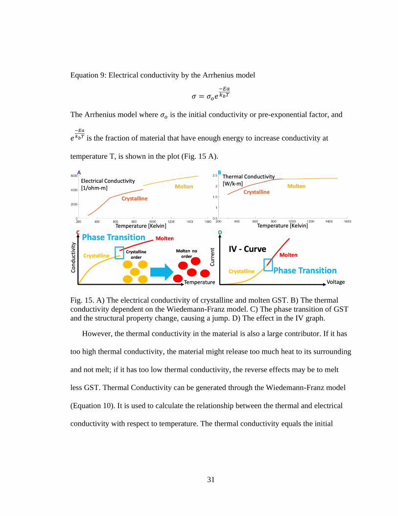
Equation 9: Electrical conductivity by the Arrhenius model
𝜎 = 𝜎𝑜𝑒−𝐸𝑎𝑘𝑏𝑇
The Arrhenius model where 𝜎𝑜 is the initial conductivity or pre-exponential factor, and
𝑒−𝐸𝑎
𝑘𝑏𝑇 is the fraction of material that have enough energy to increase conductivity at
temperature T, is shown in the plot (Fig. 15 A).
Fig. 15. A) The electrical conductivity of crystalline and molten GST. B) The thermal
conductivity dependent on the Wiedemann-Franz model. C) The phase transition of GST
and the structural property change, causing a jump. D) The effect in the IV graph.
However, the thermal conductivity in the material is also a large contributor. If it has
too high thermal conductivity, the material might release too much heat to its surrounding
and not melt; if it has too low thermal conductivity, the reverse effects may be to melt
less GST. Thermal Conductivity can be generated through the Wiedemann-Franz model
(Equation 10). It is used to calculate the relationship between the thermal and electrical
conductivity with respect to temperature. The thermal conductivity equals the initial
32
conductivity, 𝜅𝑝ℎ𝑜, added to the electrical conductivity, 𝜎, multiplied by the temperature
and Lorenz number, 𝐿, which makes up for the thermal conductivity.
Equation 10: Wiedemann-Franz model [17]
𝜅 = 𝜅𝑝ℎ𝑜 + 𝜎𝐿𝑇
However, what also needs to be considered is that the material structure properties
change between crystalline and molten phase. Seen in the plot (Fig. 15 C) is an almost
identical graph to A, which shows in blue where there is a phase transition. As the
crystalline gets hotter and hotter, it will lose its structure and at one point create a jump in
the conductivity of the material. The actual impact on the IV curve is minimal due to the
gradual change over many molecules (Fig. 15 D). However, it would be possible to be
seen if one could measure the maximum temperature of the device, due to latent heat.
Interestingly there is a difficult time to characterize molten conductivity. This is because
at nano scale, materials tend to change properties, which is not hard to measure in solid
materials, but because it acts as a liquid, researchers have lost contact with the molten
phase and have not been able to characterize its conductivity. Therefore, the simulation is
using assumptions within the molten phase.
4.2 Joule heating energy by current surge
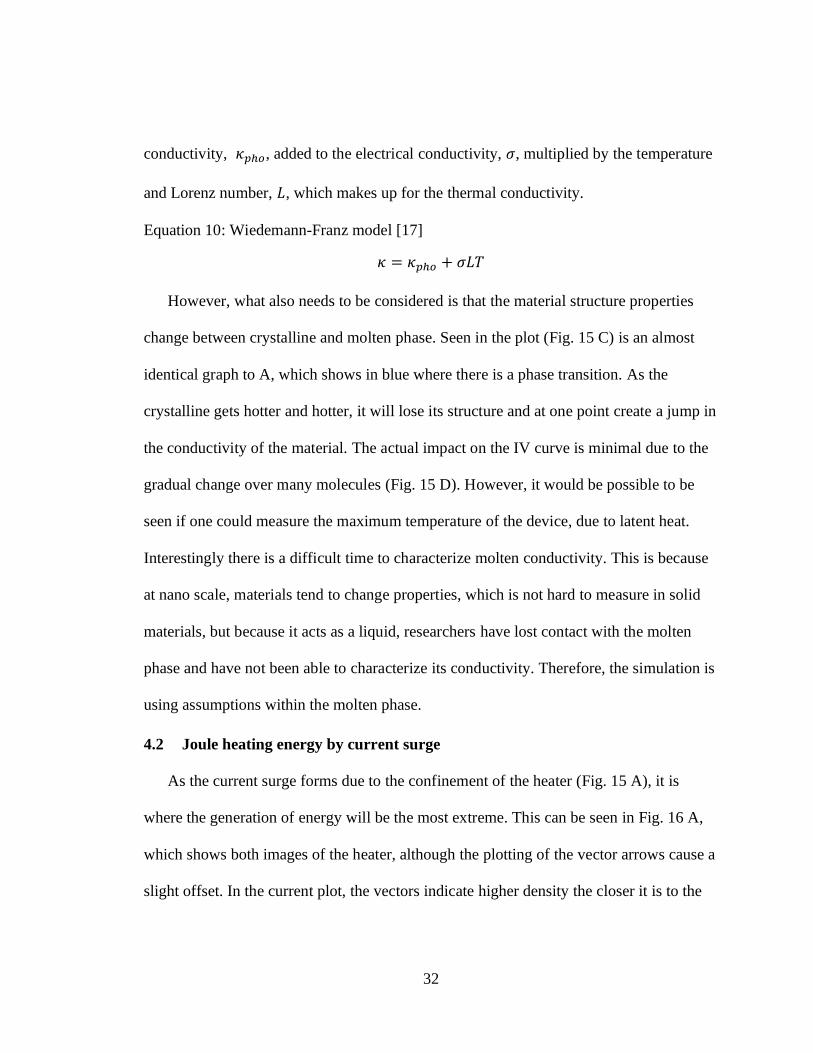
As the current surge forms due to the confinement of the heater (Fig. 15 A), it is
where the generation of energy will be the most extreme. This can be seen in Fig. 16 A,
which shows both images of the heater, although the plotting of the vector arrows cause a
slight offset. In the current plot, the vectors indicate higher density the closer it is to the
33
heater, while in the energy generation plot shining at these confinements indicates high
levels. Fig. 16 B is a large picture of the heater; here the energy is the largest at the edges
of the more conductive material and indicates that the current is coming from the outside
of the cell as it tries to flow into the narrow heater. This can clearly be seen in a Z slice
taken just inside the GST material (Fig. 16 B lower image). Again, the joule-heating is
maximum just at the very outside rim of the highest conductive path down and out of the
GST, causing temperatures to increase.
Fig. 16. A) Current flow and energy generation on top of heater. B) A closer view of the
energy from the side and top.
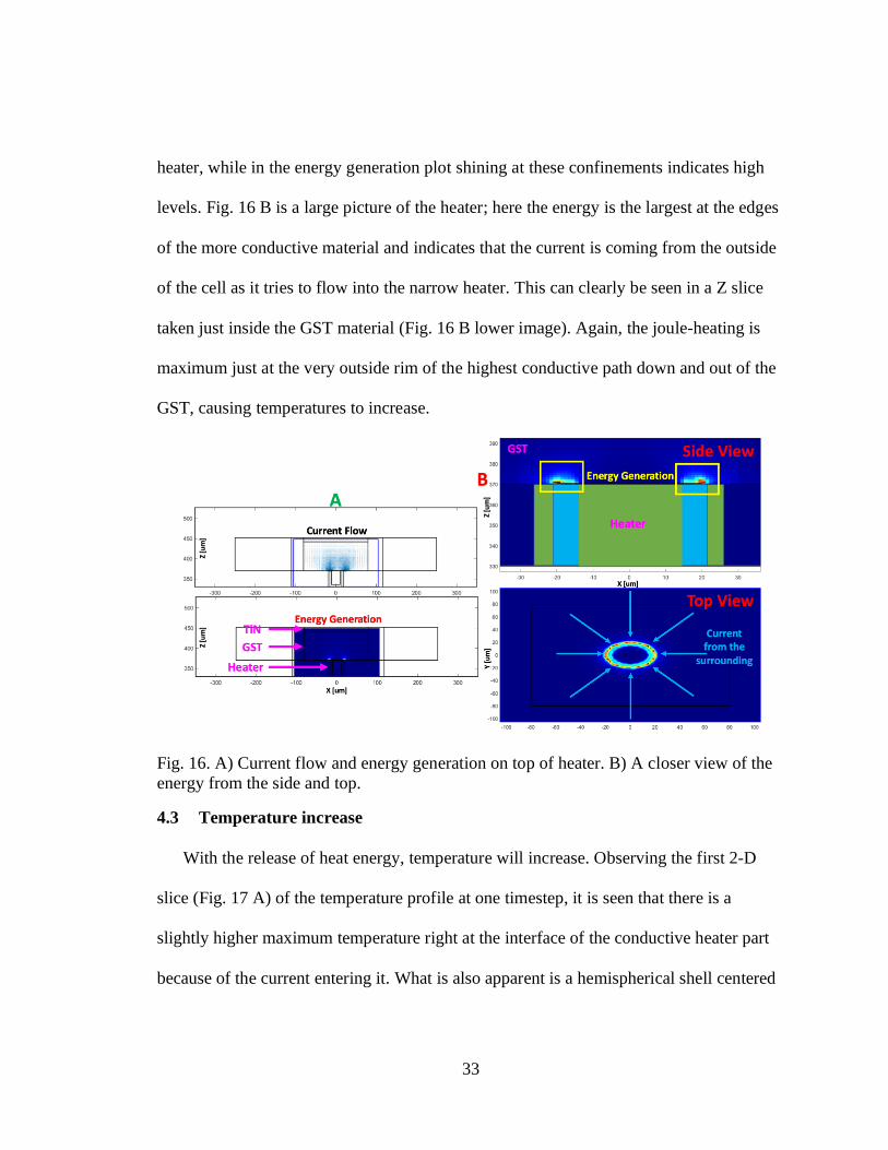
4.3 Temperature increase
With the release of heat energy, temperature will increase. Observing the first 2-D
slice (Fig. 17 A) of the temperature profile at one timestep, it is seen that there is a
slightly higher maximum temperature right at the interface of the conductive heater part
because of the current entering it. What is also apparent is a hemispherical shell centered
34
above the heater. The temperature in part A (Fig. 17) is taken at about 10 ns into a
simulation of a linearly increasing applied voltage, at a time when peak temperature is
well below melting. However, the plot indicates that the temperature is increasing at the
heater.
Fig. 17. Temperature 2D slice of simulated device, at different time intervals.
Increasing the applied voltage increases the peak temperature within the device.
However, at 116 ns it is seen that the maximum temperature has reached 600 degrees and
it seems to stay there for a few nanoseconds (Fig. 17 B). This is because the simulator
implements the latent heat of melting for GST, that is, the endothermic energy cost of
converting a solid into a liquid. Thereafter, at 124 ns (Fig. 17 C), parts of the structure
that have paid this energy cost are in the molten phase and are free to exceed 600 oC.
35
Other portions of the cell are undergoing the melting process, and as electricity is the
cause, it is important to be modeled and shown to properly follow the standard physics.
However, by continuing to ramp up the voltage, there will be larger amount of joule
heating while the simulator self-consistently solves for the dynamic resistance of the
PCM device as its local resistivity changes with temperature. As a result, it is not
expected that the IV curve of the PCM device to be a simple ohmic relation.
4.4 Arrhenius Model
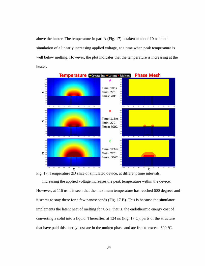
The Arrhenius-modeled electrical current is seen in the IV, resistance power (RP),
and resistance voltage (RV) graphs (Fig. 18). The experimental mean and median data
are taken by Benedict Kersting from IBM’s Zurich lab, on devices fabricated at the IBM
Albany nanotech center. Comparing the simulation result of activation energy 0.08 joule,
in red, that uses the simple model for electrical conductivity purely as a function of
temperature, it is seen that the values are a bit off. The simulated IV curve must bend up,
making the device more conductive at an earlier temperature. In the RV graph it is also
seen that the device has a too high electrical resistance compared to the experimental
device. The dynamic-resistance curve must bend down to match the experimental results,
again needing higher conductance. Observing the RP, it is clear as well, there is a need
for more conductive material.
Changing the activation energy, Ea, the conductivity changes within the device but
not nearly enough at lower applied voltages. The IV shows the increased Ea to become so
conductive that the device exhibits a thermally induced negative differential resistance. It
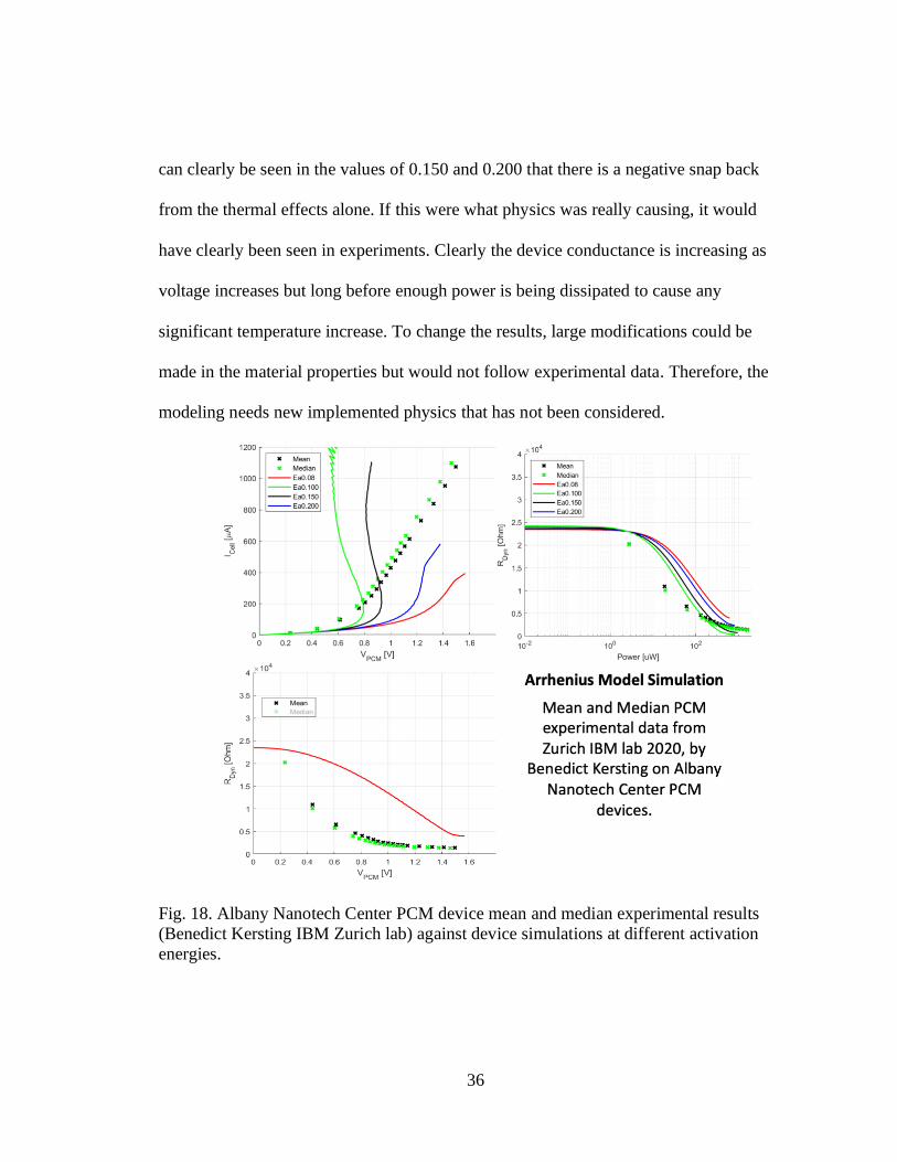
36
can clearly be seen in the values of 0.150 and 0.200 that there is a negative snap back
from the thermal effects alone. If this were what physics was really causing, it would
have clearly been seen in experiments. Clearly the device conductance is increasing as
voltage increases but long before enough power is being dissipated to cause any
significant temperature increase. To change the results, large modifications could be
made in the material properties but would not follow experimental data. Therefore, the
modeling needs new implemented physics that has not been considered.
Fig. 18. Albany Nanotech Center PCM device mean and median experimental results
(Benedict Kersting IBM Zurich lab) against device simulations at different activation
energies.
37
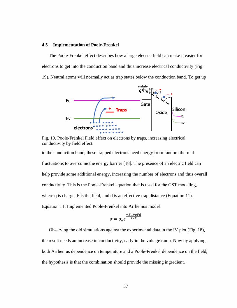
4.5 Implementation of Poole-Frenkel
The Poole-Frenkel effect describes how a large electric field can make it easier for
electrons to get into the conduction band and thus increase electrical conductivity (Fig.
19). Neutral atoms will normally act as trap states below the conduction band. To get up
Fig. 19. Poole-Frenkel Field effect on electrons by traps, increasing electrical
conductivity by field effect.
to the conduction band, these trapped electrons need energy from random thermal
fluctuations to overcome the energy barrier [18]. The presence of an electric field can
help provide some additional energy, increasing the number of electrons and thus overall
conductivity. This is the Poole-Frenkel equation that is used for the GST modeling,
where q is charge, F is the field, and d is an effective trap distance (Equation 11).
Equation 11: Implemented Poole-Frenkel into Arrhenius model
𝜎 = 𝜎𝑜𝑒−𝐸𝑎+𝑞𝐹𝑑
𝑘𝑏𝑇
Observing the old simulations against the experimental data in the IV plot (Fig. 18),
the result needs an increase in conductivity, early in the voltage ramp. Now by applying
both Arrhenius dependence on temperature and a Poole-Frenkel dependence on the field,
the hypothesis is that the combination should provide the missing ingredient.
38
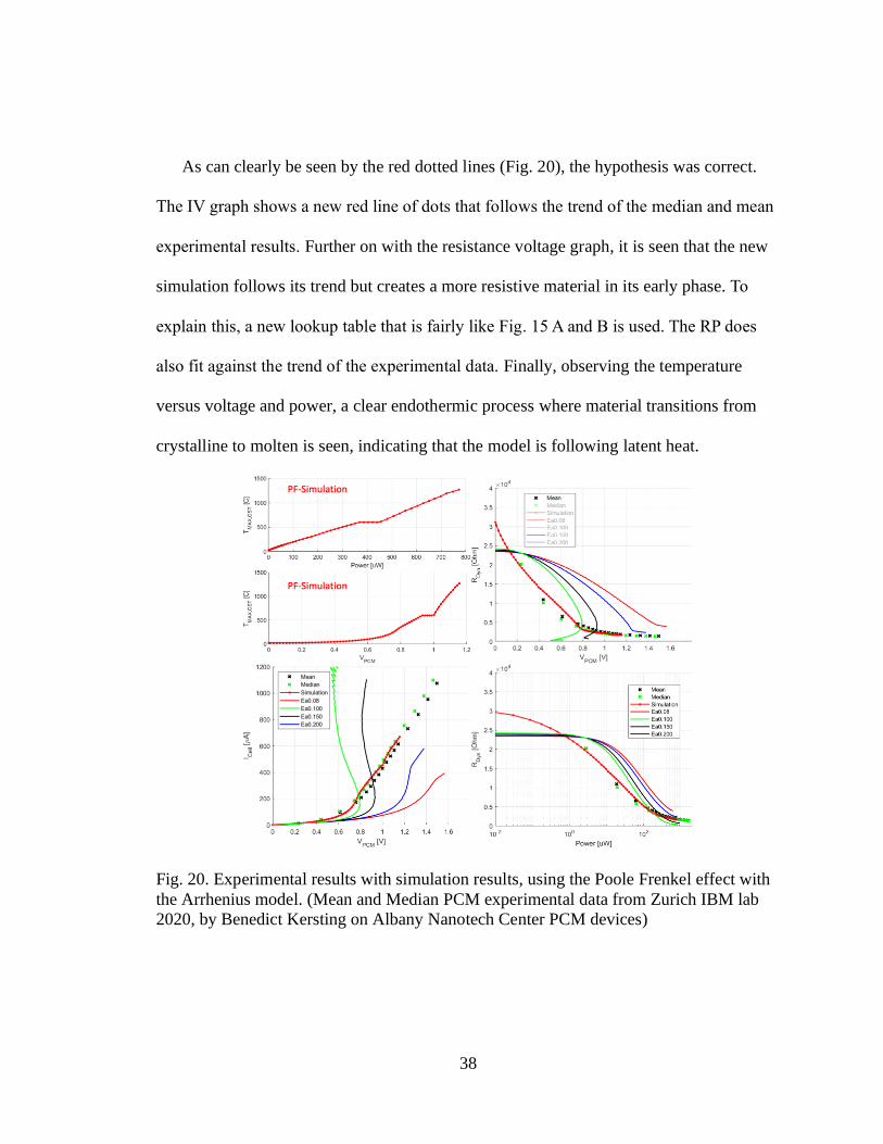
As can clearly be seen by the red dotted lines (Fig. 20), the hypothesis was correct.
The IV graph shows a new red line of dots that follows the trend of the median and mean
experimental results. Further on with the resistance voltage graph, it is seen that the new
simulation follows its trend but creates a more resistive material in its early phase. To
explain this, a new lookup table that is fairly like Fig. 15 A and B is used. The RP does
also fit against the trend of the experimental data. Finally, observing the temperature
versus voltage and power, a clear endothermic process where material transitions from
crystalline to molten is seen, indicating that the model is following latent heat.
Fig. 20. Experimental results with simulation results, using the Poole Frenkel effect with
the Arrhenius model. (Mean and Median PCM experimental data from Zurich IBM lab
2020, by Benedict Kersting on Albany Nanotech Center PCM devices)
39
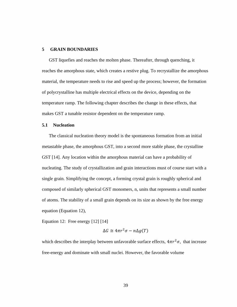
5 GRAIN BOUNDARIES
GST liquefies and reaches the molten phase. Thereafter, through quenching, it
reaches the amorphous state, which creates a restive plug. To recrystallize the amorphous
material, the temperature needs to rise and speed up the process; however, the formation
of polycrystalline has multiple electrical effects on the device, depending on the
temperature ramp. The following chapter describes the change in these effects, that
makes GST a tunable resistor dependent on the temperature ramp.
5.1 Nucleation
The classical nucleation theory model is the spontaneous formation from an initial
metastable phase, the amorphous GST, into a second more stable phase, the crystalline
GST [14]. Any location within the amorphous material can have a probability of
nucleating. The study of crystallization and grain interactions must of course start with a
single grain. Simplifying the concept, a forming crystal grain is roughly spherical and
composed of similarly spherical GST monomers, n, units that represents a small number
of atoms. The stability of a small grain depends on its size as shown by the free energy
equation (Equation 12),
Equation 12: Free energy [12] [14]
∆𝐺 ≅ 4𝜋𝑟2𝜎 − 𝑛∆𝑔(𝑇)
which describes the interplay between unfavorable surface effects, 4𝜋𝑟2𝜎, that increase
free-energy and dominate with small nuclei. However, the favorable volume
40
effects, ∆𝑔(𝑇), decrease the free-energy with monomer counts and dominate with a large
nuclei [9] [14].
When a single crystalline nuclei is small or sub-critical, it is more likely to shrink
than it is to grow. In this phase, the free-energy difference of growing and shrinking by
the monomer unit determines the rates of growth and decay in the sub-critical phase.
Once a nuclei gets over the critical size, nc, where volume effects overtake surface
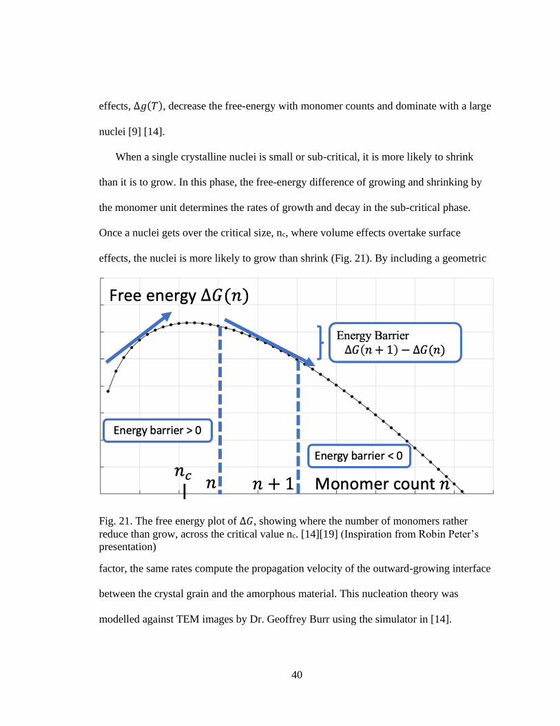
effects, the nuclei is more likely to grow than shrink (Fig. 21). By including a geometric
Fig. 21. The free energy plot of ∆𝐺, showing where the number of monomers rather
reduce than grow, across the critical value nc. [14][19] (Inspiration from Robin Peter’s
presentation)
factor, the same rates compute the propagation velocity of the outward-growing interface
between the crystal grain and the amorphous material. This nucleation theory was
modelled against TEM images by Dr. Geoffrey Burr using the simulator in [14].
41
However, the effect on the electrical conductivity by polycrystalline material was never
discussed.
5.2 Grain boundaries and electrical conductivity
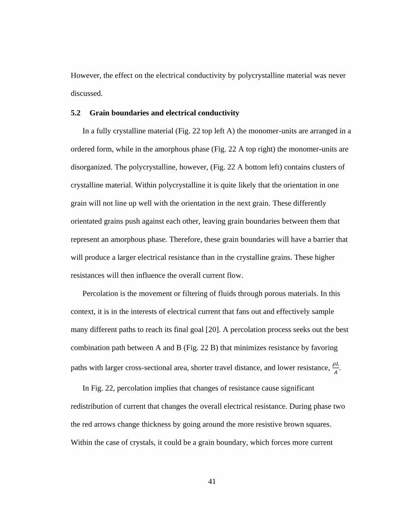
In a fully crystalline material (Fig. 22 top left A) the monomer-units are arranged in a
ordered form, while in the amorphous phase (Fig. 22 A top right) the monomer-units are
disorganized. The polycrystalline, however, (Fig. 22 A bottom left) contains clusters of
crystalline material. Within polycrystalline it is quite likely that the orientation in one
grain will not line up well with the orientation in the next grain. These differently
orientated grains push against each other, leaving grain boundaries between them that
represent an amorphous phase. Therefore, these grain boundaries will have a barrier that
will produce a larger electrical resistance than in the crystalline grains. These higher
resistances will then influence the overall current flow.
Percolation is the movement or filtering of fluids through porous materials. In this
context, it is in the interests of electrical current that fans out and effectively sample
many different paths to reach its final goal [20]. A percolation process seeks out the best
combination path between A and B (Fig. 22 B) that minimizes resistance by favoring
paths with larger cross-sectional area, shorter travel distance, and lower resistance, 𝜌𝐿
𝐴.
In Fig. 22, percolation implies that changes of resistance cause significant
redistribution of current that changes the overall electrical resistance. During phase two
the red arrows change thickness by going around the more resistive brown squares.
Within the case of crystals, it could be a grain boundary, which forces more current
42
through a smaller area. The changes can have large impacts, and if the more resistive
material disappears it will therefore change the reading of the material. This concept can
be compared to the polycrystalline forming and changing, while heating up an amorphous
material.
Fig. 22. A) The crystal structure of crystalline, amorphous, and polycrystalline, where the
pink line indicates a grain boundary. [21] B) Percolation through a medium with
changing resistance.
5.3 Grain Formation
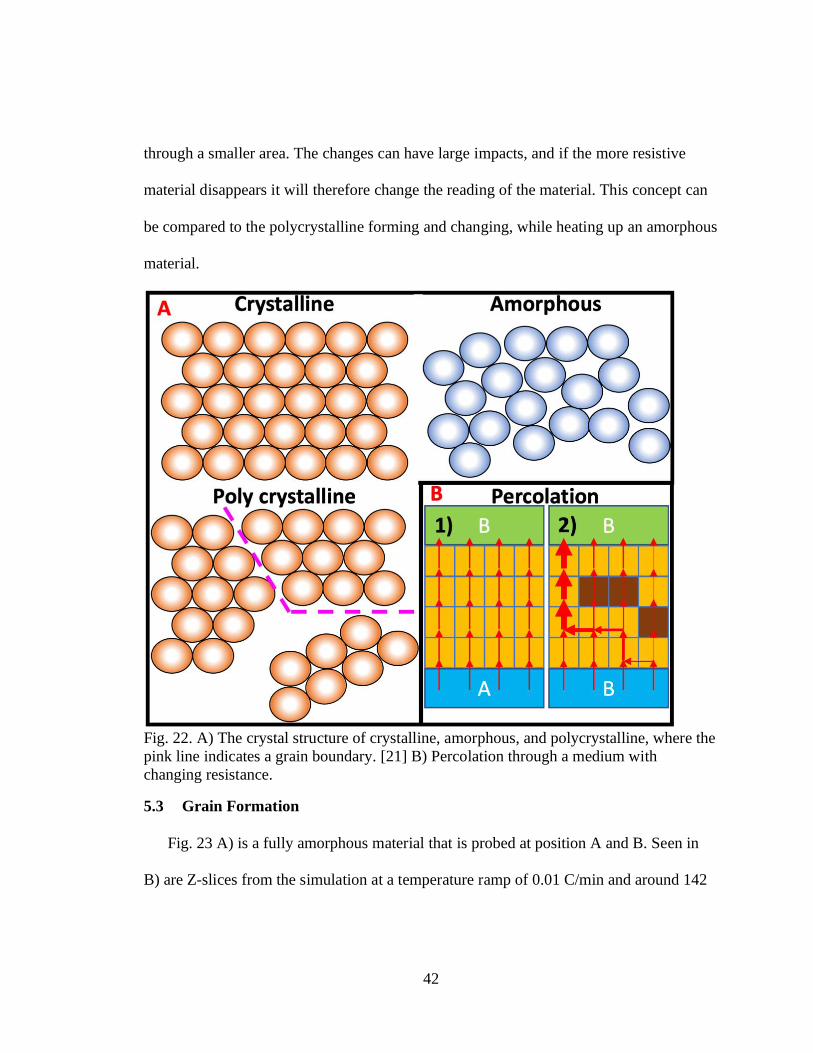
Fig. 23 A) is a fully amorphous material that is probed at position A and B. Seen in
B) are Z-slices from the simulation at a temperature ramp of 0.01 C/min and around 142
43
hours into the simulation. The bottom three graphs represent the phase of the material and
the left most graph of the light blue is amorphous. As temperature increases, a
crystallization process occurs (Set Operation). Yellow shows fully crystalline voxels, and
brown voxels represent freely moving crystal growth fronts, while dark blue indicates the
amorphous like grain boundaries where two or more different grains have run into each
other.
Fig. 23. A) A slab of phase change material with an anode and cathode probed. B) The
resulting crystallization over time at a ramp of 0.01C/min. Showing the grain ids on top
and the phase on the bottom. (Crystalline = yellow, Blue=Amorphous, Dark blue = GB,
Brown= Growth front)
44
Within the simulator, each voxel tracks its own histogram of sub-critical nuclei and
models the stochastic transitions between these states [14]. Once a nuclei is lucky enough
to become super-critical, the simulation continues to track its spherical expansion until it
starts to protrude into, infect, and crystallize neighboring voxels. At the end of the
simulation (the most right graph) all the amorphous material has been converted to
crystalline, resulting in multiple grains. The simulator tracks each grain with its own ID,
making it easy to flag them and measure their size (Fig. 23). Because the simulation was
at such a low temperature ramp, there are few polycrystalline grains formed; however, by
increasing the temperature ramp they will increase.
Motivated by Dr. Burr’s 2012 paper [14], the study increases the temperature ramp to
change the grain sizes. At a temperature ramp of 0.01 C/min, fewer crystals are forming
in comparison to the 1C/min ramp (Fig. 24). By increasing the ramp to 100C/min, the
number of crystalline grains grows. In the 2012 paper, Dr. Burr showed that this effect
arises from the fact that nucleation and growth both grow exponentially as a function of
temperature, but at different slopes [14]. Thus, a slow temperature ramp rate means that
the first nucleating grains have plenty of time to grow and consume vast amounts of
territory, leading to large grains. A fast temperature ramp does increase the speed at
which the first nucleating grains can grow; however, it does also make it quite likely that
a new grain will nucleate directly in its path, cutting off its ability to grow large.
Furthermore, it is well observed that crystallization happens later in the temperature
perspective as the crystalline grains are trying to keep up, letting more amorphous
45
material be exposed to energy, therefore creating stable grains. For the thesis purpose,
fluctuating the temperature ramp changes the number of grain boundaries and can
hypothetically do the same to the electrical resistance.
Fig. 24. Crystallization fraction of temperature ramps at 0.01, 1, and 100 C/minute.
Determining the temperature ramps effect on the amount of polycrystalline.
5.4 Polycrystalline electrical conductivity
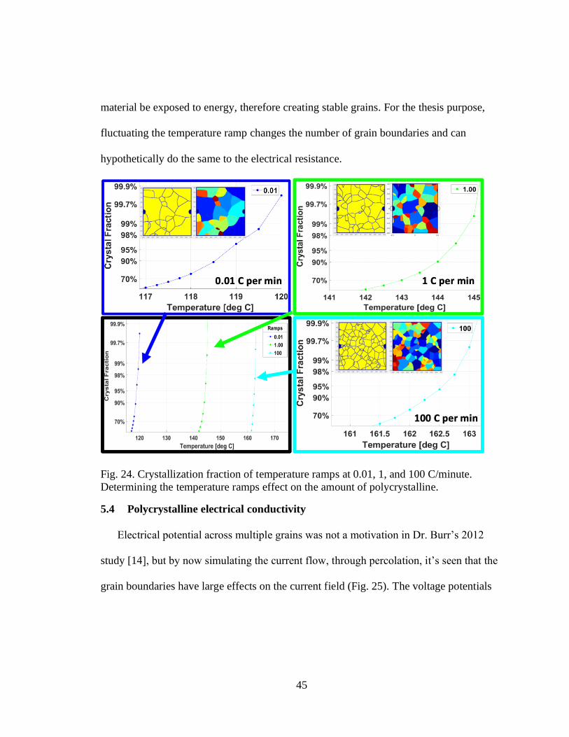
Electrical potential across multiple grains was not a motivation in Dr. Burr’s 2012
study [14], but by now simulating the current flow, through percolation, it’s seen that the
grain boundaries have large effects on the current field (Fig. 25). The voltage potentials
46
are at 0 and 1 (Fig. 25 B), and it’s clearly seen that the current vectors (Fig. 25 D) pass
through the least amount of grain boundaries (Fig. 25 A).
The resistance plot flattens at a fraction of 0.55 (Fig. 25 C), therefore having already
found the least resistive path through the smallest amount of grain boundaries. The
simulator uses three constant conductivities for the crystal-grain, grain-boundary, and
amorphous material, which are held constant even as temperature ramps up. The
conductivities represent the expected effect on the read current if the ramp was to stop
and cool back down to room temperature.
Fig. 25. A) Polycrystalline cell state B) potential drop, C) electrical conductivity (top)
changes with crystal fraction growth (bottom), and D) current field map.
47
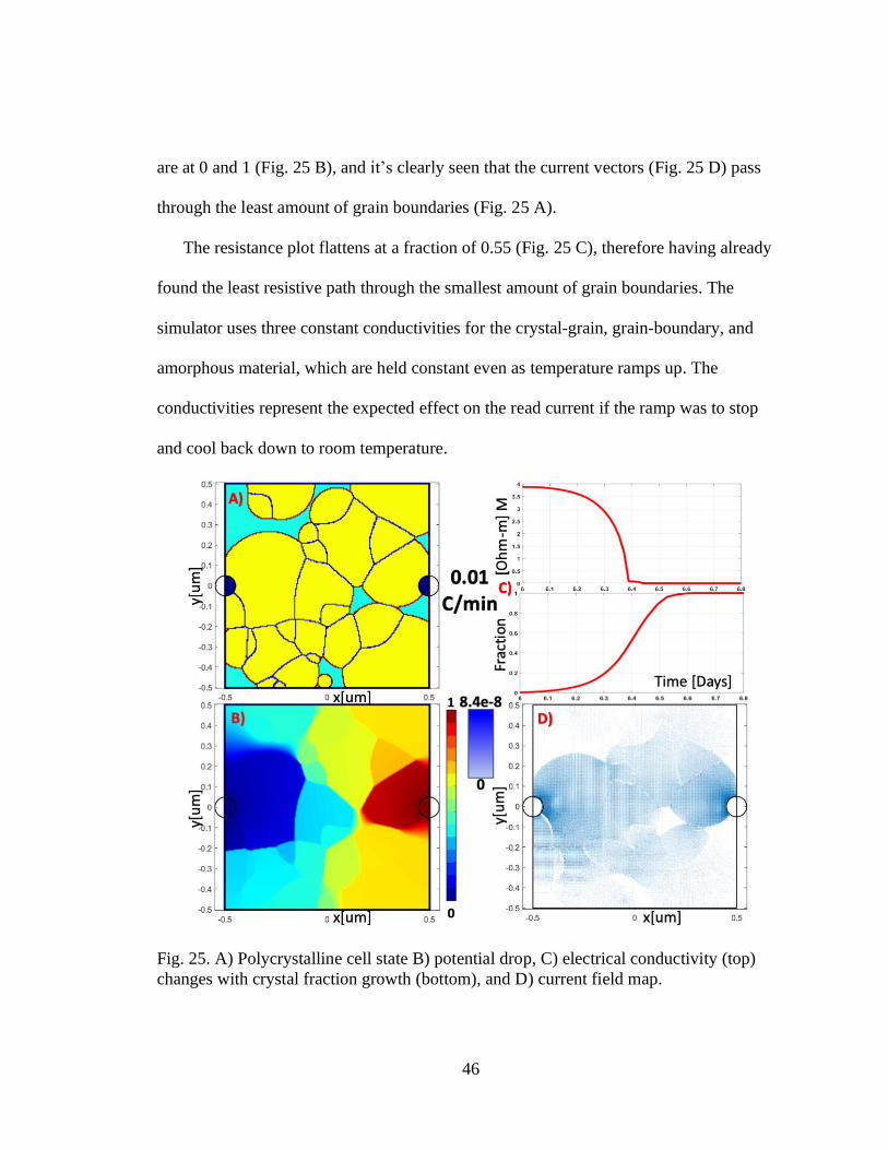
Increasing the temperature ramps should now do the same to the resistance to agree
with the hypothesis. Fig. 26 represents the crystal fraction versus the resistance. It focuses
on the end of the simulation where it has reached steady state and nothing else is
changing. The material is following the expected trend; the fast ramp rate that led to
small grains has high resistance due to many grain boundaries, while the slower ramp-
rates led to large grains has low resistance due to fewer grain boundaries.
Fig. 26. Electrical resistance change against crystal fraction growth with different
temperature ramps.
48
6 CONCLUSION
In conclusion, the thesis has introduced the studies of PCM devices, discussed the
simulators’ ability to calculate the thermal and voltage distribution through Douglas-
Gunn ADI method, simulated one dimensional and third dimensional thermal diffusion
against literate and the standard industry tool ANSYS, fitted simulations against
experimental PCM device IV data by including new physics, and finally shown the
impact and importance that grain boundaries has on intermediate resistance operations.
Therefore, the thesis has shown how important and useful it is to simulate PCM devices
for the future of Analog AI device research.
Future work would include more physics that correctly model the molten PCM, as
assumptions were used to simulate the IV plots. Additionally, future students who visit
IBM could develop the actual grain boundary interactions in the PCM cell.
49
Literature Cited
[1] Reinsel, D., Gantz, J., & Rydning, J. (2018). The Digitization of the World – From
Edge to Core. Needham, MA: IDC. doi:#US44413318
[2] Kavlakoglu, E. (2020, May 27). Ai vs. machine learning vs. deep learning vs.
neural networks: What's the difference? Retrieved March 16, 2021, from
https://www.ibm.com/cloud/blog/ai-vs-machine-learning-vs-deep-learning-vs-
neural-networks
[3] Lanzetta, M. (2018). Machine learning, deep learning, and artificial
intelligence. Artificial Intelligence for Autonomous Networks, 25-47.
doi:10.1201/9781351130165-2
[4] Meng, Z., Hu, Y., & Ancey, C. (2020). Using a data driven approach to predict
waves generated by gravity driven mass flows. Water, 12(2), 600.
doi:10.3390/w12020600
[5] Burr, G. W., Narayanan, P., Shelby, R. M., Sidler, S., Boybat, I., Di Nolfo, C., &
Leblebici, Y. (2015). Large-scale neural networks implemented with non-volatile
memory as the synaptic weight element: Comparative performance analysis
(accuracy, speed, and power). 2015 IEEE International Electron Devices Meeting
(IEDM). doi:10.1109/iedm.2015.7409625
[6] Tsai, H., Ambrogio, S., Narayanan, P., Shelby, R. M., & Burr, G. W. (2018).
Recent progress in analog memory-based accelerators for deep learning. Journal of
Physics D: Applied Physics, 51(28), 283001. doi:10.1088/1361-6463/aac8a5
[7] Ambrogio, S., Narayanan, P., Tsai, H., Shelby, R. M., Boybat, I., Di Nolfo, C., . . .
Burr, G. W. (2018). Equivalent-accuracy accelerated neural-network training using
analogue memory. Nature, 558(7708), 60-67. doi:10.1038/s41586-018-0180-5
[8] Burr, G. W. (2008, June 6). Storage Class Memory. Lecture presented at Storage
Class Memory - Stanford in Stanford, Palo Alto.
[9] Burr, G. W. (2013, February 12). Towards Storage Class Memory: 3-D crosspoint
access devices using Mixed-Ionic-Electronic- Conduction (MIEC) , IBM Research
– Almaden
[10] Kersting, B., Ovuka, V., Jonnalagadda, V. P., Sousa, M., Bragaglia, V., Sarwat, S.
G., . . . Sebastian, A. (2020). State dependence and temporal evolution of resistance
50
in projected phase change memory. Scientific Reports, 10(1). doi:10.1038/s41598-
020-64826-3
[11] Raoux, S., Xiong, F., Wuttig, M., & Pop, E. (2014). Phase change materials and
phase change memory. Materials Research Society, 39, 703-709.
doi:10.1557/mrs.2014.139
[12] Le Gallo, M., & Sebastian, A. (2020). An overview of phase-change memory
device physics. Journal of Physics D: Applied Physics, 53(21), 213002.
doi:10.1088/1361-6463/ab7794
[13] Lee, B., Shelby, R. M., Raoux, S., Retter, C. T., Burr, G. W., Bogle, S. N., . . .
Abelson, J. R. (2014). Nanoscale nuclei in phase change materials: Origin of
different crystallization mechanisms of ge2sb2te5 and aginsbte. Journal of Applied
Physics, 115(6), 063506. doi:10.1063/1.4865295
[14] Burr, G. W., Tchoulfian, P., Topuria, T., Nyffeler, C., Virwani, K., Padilla, A., . . .
Lee, B. (2012). Observation and modeling of polycrystalline grain formation in
ge2sb2te5. Journal of Applied Physics, 111(10), 104308. doi:10.1063/1.4718574
[15] Ting-Yuan Wang and Charlie C.P Chen, “3-D Thermal-ADI: A Linear-Time Chip
Level Transient Thermal Simulator”, IEEE transactions on computer-aided design
of integrated circuits and system, VOL, 21, NO. 12, December 2002.
doi: 10.1109/TCAD.2002.804385
[16] Schwartz, P., Barad, M., Colella, P., & Ligocki, T. (2006). A Cartesian grid
embedded BOUNDARY method for the heat equation and Poisson’s equation in
three dimensions. Journal of Computational Physics, 211(2), 531-550.
doi:10.1016/j.jcp.2005.06.010
[17] Mizuno, N., Kosai, S., & Yamasue, E. (2020). Applicability of Wiedemann-Franz
law to thermal conductivity of molten Field’s Metal. Materials Science Forum, 985,
1-9. doi:10.4028/www.scientific.net/msf.985.1
[18] Schroeder, H. (2015). Poole-Frenkel-effect as dominating current mechanism in
thin OXIDE FILMS—AN ILLUSION?! Journal of Applied Physics, 117(21),
215103. doi:10.1063/1.4921949
[19] Schmelzer, J. W. (2010). On the determination of the kinetic pre-factor in classical
nucleation theory. Journal of Non-Crystalline Solids, 356(52-54), 2901-2907.
doi:10.1016/j.jnoncrysol.2010.02.026
51
[20] Last, B. J., & Thouless, D. J. (1971). Percolation theory and electrical
conductivity. Physical Review Letters, 27(25), 1719-1721.
doi:10.1103/physrevlett.27.1719
[21] Li, Z., Lee, J., Reifenberg, J. P., Asheghi, M., Jeyasingh, R. G., Wong, H. P., &
Goodson, K. E. (2011). Grain boundaries, Phase impurities, and Anisotropic
thermal conduction IN Phase-Change Memory. IEEE Electron Device
Letters,32(7), 961-963. doi:10.1109/led.2011.2150193