Embed Size (px)
Citation preview

Ministry of Education and Science of the Russian Federation Saint Petersburg National Research University of Information
Technologies, Mechanics, and Optics
NANOSYSTEMS: PHYSICS, CHEMISTRY, MATHEMATICS
2014, volume 5 (6)
Наносистемы: физика, химия, математика 2014, том 5, 6
NANOSYSTEMS: PHYSICS, CHEMISTRY, MATHEMATICS
ADVISORY BOARD MEMBERS Chairman: V.N. Vasiliev (St. Petersburg, Russia), V.M. Ievlev (Voronezh), P.S. Kop’ev(St. Petersburg, Russia), V.N. Parmon (Novosibirsk), A.I. Rusanov (St. Petersburg, Russia).
EDITORIAL BOARD Editor-in-Chief: N.F. Morozov (St. Petersburg, Russia) Deputy Editor-in-Chief: I.Yu. Popov (St. Petersburg, Russia)
Section Co-Editors: Physics – V.M. Uzdin (St. Petersburg, Russia), Chemistry, material science –V.V. Gusarov (St. Petersburg, Russia), Mechanics – A.K. Belyaev (St. Petersburg, Russia), Mathematics – I.Yu. Popov (St. Petersburg, Russia).
Editorial Board Members: V.M. Adamyan (Odessa, Ukraine); O.V. Al’myasheva (St. Petersburg, Russia); S. Bechta (Stockholm, Sweden); V.G. Bespalov (St. Petersburg, Russia); A. Chatterjee (Hyderabad,
India); S.A. Chivilikhin (St. Petersburg, Russia); A.V. Chizhov (Dubna, Russia); P.P. Fedorov (Moscow, Russia); E.A. Gudilin (Moscow, Russia); D.A. Indeitsev (St. Petersburg, Russia); H. Jónsson (Reykjavik, Iceland); A.A. Kiselev (Madison, USA); Yu.S. Kivshar (Canberra, Australia); S.A. Kozlov (St. Petersburg, Russia); Yu.B. Kudasov (Sarov, Russia); S.E. Kul’kova (Tomsk, Russia); P.A. Kurasov (Stockholm, Sweden); A.V. Lukashin (Moscow, Russia); V.A. Margulis (Saransk, Russia); I.V. Melikhov (Moscow,
Russia); G.P. Miroshnichenko (St. Petersburg, Russia); H. Neidhardt (Berlin, Germany); K. Pankrashkin (Orsay, France); B.S. Pavlov (Auckland, New Zealand); A.V. Ragulya (Kiev,
Ukraine); V. Rajendran (Tamil Nadu, India); A.A. Rempel (Ekaterinburg, Russia); V.P. Romanov (St. Petersburg, Russia); V.Ya. Rudyak (Novosibirsk, Russia); V.M. Talanov (Novocherkassk, Russia); A.Ya. Vul’ (St. Petersburg, Russia).
Editors: I.V. Blinova; A.I. Popov; A.I. Trifanov; E.S. Trifanova (St. Petersburg, Russia),
R. Simoneaux (USA).
Address: University ITMO, Kronverkskiy pr., 49, St. Petersburg 197101, Russia. Phone: +7(812)232-67-65, Journal site: http://nanojournal.ifmo.ru/, E-mail: [email protected]
AIM AND SCOPE The scope of the journal includes all areas of nano-sciences. Papers devoted to basic problems of physics, chemistry, material science and mathematics inspired by nanosystems investigations are welcomed. Both theoretical and experimental works concerning the properties and behavior of nanosystems, problems of its creation and application, mathematical methods of nanosystem studies are considered. The journal publishes scientific reviews (up to 30 journal pages), research papers (up to 15 pages) and letters (up to 5 pages). All manuscripts are peer-reviewed. Authors are informed about the referee opinion and the Editorial decision.
N A N O
Ф &Х &М
Content PHYSICS M.R. Mohebbifar, M. Ahmadi daryakenari, G. Mosallanezhad, M. Zohrabi Effect of the elimination of the barrier layer period in productive process and its simulation of absorption spectra for anodic alumina membrane 737 S.Kh. Batygov, M.N. Mayakova, S.V. Kuznetsov, P.P. Fedorov X-ray luminescence of BaF2:Ce3+ powders 752 P.F. Bessarab, A. Skorodumov, V. M. Uzdin, H. Jónsson Navigation on the energy surface of the noncollinear Alexander-Anderson model 757 A.A. Bogdanov, S.P.Denisov, A.A. Karetnikov, A.P.Kovshik, V.P.Romanov, D. Brukkel The effect of the cell phone radiation on a freely suspended liquid-crystal film 782 V.F. Gremenok, V.A. Ivanov, H. Izadneshan, V.V. Lazenka, A. Bakouie Physical properties of hot wall deposited Sn1-xPbxS thin films 789 M.A. Jafarov, E.F. Nasirov, R. Mammadov, R. Jafarli Fabrication and Characterization ZnCdS nanowire 796 A.V. Kalenskii, M.V. Ananyeva Spectral regularities of the critical energy density of the pentaerythriol tetranitrate- aluminum nanosystems initiated by the laser pulse 803 V.V. Zakharov, M.A. Baranov, A.S. Zlatov, A.V. Veniaminov Measuring local quantum yield of photoluminescence and phototransformations with laser scanning microscope 811
CHEMISTRY AND MATERIAL SCIENCE Bassem Assfour, Thaer assaad, adnan odeh Hydrogen adsorption properties of metal-organic frameworks within the density-functional based tight-binding approach 820 Jun Li, Zhen Hu, Yuanjun Song, Yudong Huang, V.V. Zuev New route to poly (2, 6 – diimidaazo (4,5-b: 4’,5’ - e) pyridinelene-1,4 (2,5-dihydroxy)-phenylene) (pipd) and high modulus fiber on it basis 829 N.A. Lomanova Dielectric properties of Aurivillius phase Bi10Fe6Ti3O30 with a nano-sized pseudo-perovskite blocks 836 Sidheshwar G. Gaurkhede Synthesis and studies room temperature conductivity, dielectric analysis of LaF3 nanocrystals 843 V.V. Sokolov, N.A. Petrov, M.V. Tomkovich, V.V. Gusarov Porous structure of carbon nanoparticles prepared by chlorination of nanoparticles of silicon carbid 849 Е.А. Тugova, O.N. Karpov Nanocrystalline perovskite-like oxides formation in Ln2O3 – Fe2O3 – H2O (Ln = La, Gd) systems 854 Information for authors 861
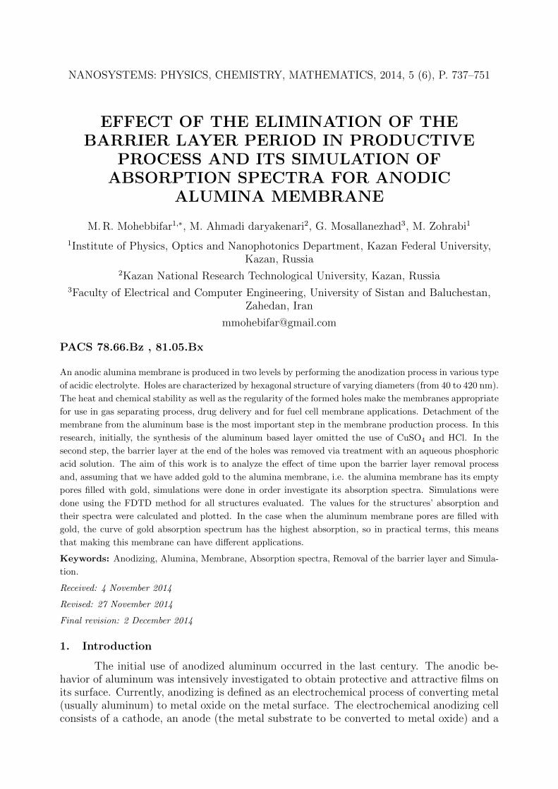
NANOSYSTEMS: PHYSICS, CHEMISTRY, MATHEMATICS, 2014, 5 (6), P. 737–751
EFFECT OF THE ELIMINATION OF THEBARRIER LAYER PERIOD IN PRODUCTIVE
PROCESS AND ITS SIMULATION OFABSORPTION SPECTRA FOR ANODIC
ALUMINA MEMBRANE
M. R. Mohebbifar1,∗, M. Ahmadi daryakenari2, G. Mosallanezhad3, M. Zohrabi1
1Institute of Physics, Optics and Nanophotonics Department, Kazan Federal University,Kazan, Russia
2Kazan National Research Technological University, Kazan, Russia3Faculty of Electrical and Computer Engineering, University of Sistan and Baluchestan,
Zahedan, Iran
PACS 78.66.Bz , 81.05.Bx
An anodic alumina membrane is produced in two levels by performing the anodization process in various type
of acidic electrolyte. Holes are characterized by hexagonal structure of varying diameters (from 40 to 420 nm).
The heat and chemical stability as well as the regularity of the formed holes make the membranes appropriate
for use in gas separating process, drug delivery and for fuel cell membrane applications. Detachment of the
membrane from the aluminum base is the most important step in the membrane production process. In this
research, initially, the synthesis of the aluminum based layer omitted the use of CuSO4 and HCl. In the
second step, the barrier layer at the end of the holes was removed via treatment with an aqueous phosphoric
acid solution. The aim of this work is to analyze the effect of time upon the barrier layer removal process
and, assuming that we have added gold to the alumina membrane, i.e. the alumina membrane has its empty
pores filled with gold, simulations were done in order investigate its absorption spectra. Simulations were
done using the FDTD method for all structures evaluated. The values for the structures’ absorption and
their spectra were calculated and plotted. In the case when the aluminum membrane pores are filled with
gold, the curve of gold absorption spectrum has the highest absorption, so in practical terms, this means
that making this membrane can have different applications.
Keywords: Anodizing, Alumina, Membrane, Absorption spectra, Removal of the barrier layer and Simula-
tion.
Received: 4 November 2014
Revised: 27 November 2014
Final revision: 2 December 2014
1. Introduction
The initial use of anodized aluminum occurred in the last century. The anodic be-havior of aluminum was intensively investigated to obtain protective and attractive films onits surface. Currently, anodizing is defined as an electrochemical process of converting metal(usually aluminum) to metal oxide on the metal surface. The electrochemical anodizing cellconsists of a cathode, an anode (the metal substrate to be converted to metal oxide) and a
738 M. R. Mohebbifar, M. Ahmadi daryakenari, et al.
direct current (DC) power supply. The anodic aluminum oxide thin film starts to grow atthe anode (aluminum surface) as the anodic current or voltage is applied [1, 2].
An anodic alumina membrane (AAM) can provide a simple template for the depo-sition and growth of various materials with ordered structure. A new bi-level method ofanodizing for the synthesis of porous aluminum oxide with regular structure in oxalic acidwas invented by H. Masuda in 1995 [3]. Since then, scientists have tried to discover newways to synthesize this structure with different features.
The success of anodic alumina membrane is owed to its attractive physical and chem-ical properties: its ceramic temperament involves high thermal strength (up to several hun-dred degrees) and excellent chemical insensitivity in many environments (within the pHrange of 5 to 9). It has highly-ordered nanopores with controllable and uniform dimensionsarranged in a close-packed hexagonal framework. Anodic alumina membranes with pore di-ameters ranging from 4 nm to 420 nm, density as high as 1011 pores/cm2, and film thicknessvariable from 0.1 µm to 300 µm has been obtained using two-step anodization or nanoim-print methods. These materials can be synthesized in slightly soluble electrolytes such assulfuric, phosphoric and oxalic acids [4, 5].
The synthesis of nanomaterials such as polymeric nanowire, metallic nanowire [6], 3Dnanodots [7], polymeric [8] and metallic nanotubes [9] and others provides many potentialresearch directions for anodic alumina membrane, also because it can be used as membranein various applications such as gas separation [10], drug delivery [11], membrane in solid acidfuel cell [12] and solar cells [13].
A key difficulty encountered in the above-mentioned applications is how to attainthrough-hole porous anodic alumina which is previously produced on an alumina barrierlayer covering aluminum substrate in the anodization process. Wet chemical etching, basedon H3PO4, is commonly viewed as the most reliable method for custom pore opening of AAM[14, 15]. The difficulty of this method is that the process of pore opening is controlled by theetching time, usually from 50–90 minutes. Different etching conditions such as concentrationof H3PO4 (5–10 wt %), temperatures (25–50C) have been reported for pore opening of AAM,but there are no details on how these variations affect the pore diameters of AAM [14,15].One aim of this work is to analyze the effect of time on the barrier layer removal process.Another aim is to perform simulations assuming that gold has been added to the membrane,i.e. the empty pores are filled with gold, in order investigate its absorption spectra. Themorphological modifications were monitored by Scanning Electron Microscopy (SEM) andClemex software.
A hemispherical shell with homogeneous thickness known as the barrier layer developsat the bottom of every nanopore during the anodization process. To date, this barrier layerhas not attracted much attention in the literature, even though many applications require itsremoval to create through-hole membranes. Examples for such applications include energy-efficient gas separation and pattern-transfer masks for e-beam evaporation,[16] reactive ionetching,[17] or molecular-beam epitaxial growth.[18] Through a carefully controlled barrierlayer etching process, one can systematically prepare a tunable pore opening. Three methodshave been used to open the barrier oxide layer: wet chemical etching,[3,20] ion milling,[19]and plasma etching.[17] Of these, the wet etching has been regarded as difficult to control andonly ion milling has received more detailed analysis in the literature.[19] Both ion milling andplasma etching have the advantage of maintaining intact pores after barrier layer removal, butrequire expensive equipment, and a typical setup allows only a small area around 1 x 1 mmto be removed at any given time and, thus, they are cost- and time-intensive. Wet chemicaletching, when properly controlled, can be used to etch samples with larger dimensions (for
Effect of the elimination of the barrier layer period... 739
example, 2 x 2 cm) and is fast, convenient, inexpensive, and reliable. This method hasbeen used routinely in our laboratory for opening the barrier layers of AAO membranes.Experimental results show that if the chemical etching is done with proper control, 10–95 nm openings in the barrier layer can be obtained systematically for AAO membranesgenerated in oxalic acid. In addition, very interesting double hexagon nanostructures wereobserved for the first time through AFM imaging before complete removal of the barrierlayer. These nanostructures reveal the impurity distribution in the membranes that bearsignificant implication for catalysis and sensing applications [21].
During anodization, a U-shaped aluminum oxide layer or barrier layer with a thicknessof 30–40 nm forms at the bottom of every nanopore. A protective polymer layer made ofa mixture of nitrocellulose and polyester resin was coated on the top surface of the AAOmembrane that is opposite to the barrier layer to prevent overetching of the surface structureand uneven diffusion of acid into the nanopores.[22]
2. AAO Barrier Layer
2.1. AAO Barrier Layer Opening
In addition, the membrane was then immersed in 200 mL of 5.00 wt% phosphoricacid at 30.0C for different periods of time, rinsed with distilled water, and dried underambient conditions. The barrier layer removal and pore widening process was then studiedwith use of atomic force microscopy (AFM) (Digital Instruments, Dimension 3000 with atype IIIa controller and TESP Si cantilevers) and SEM (Hitachi S-4700-II). Effective porediameters were determined by analyzing the total pore area of each image using Scion Imagebased on NIH Image to ascertain the average area per pore and, hence, the average porediameter [21].
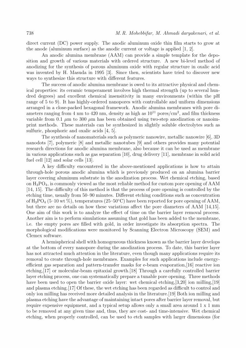
This study utilizes a freestanding anodic aluminum oxide (AAO) film with a pro-tective polymer layer made of a mixture of nitrocellulose and polyester resin on the porousside of the film [22]. The polymer layer is used to block the pores and thus prevent un-even etching of the AAO barrier layer from inside, which may be caused by the unevenacid diffusion through the AAO pores. The presence of the protective layer also focuses theetching process on the bottom side of the barrier layer, which is comprised of a hexagonallyclose packed array of hemispherical domes that are 120 nm in diameter and 27 nm in height(Fig. 1a). The domes begin to shrink both in diameter and height once the etching processstarts. After 18 min of etching, the domes have decreased in size to approximately 100 nmin diameter and 24 nm in height (Fig. 1b). It is interesting to note that, at this early stage ofthe etching process, the walls of each individual cell are becoming more pronounced, whichsuggests that the area in-between individual domes is not etched as quickly as the domesthemselves. This trend continues through 30 min of etching, with the domes continuing todecrease in size (85 nm in diameter and 16 nm in height) and the hexagonal cell walls becom-ing clearly visible to form a double hexagon nanostructure (Fig. 1c). After 40 min of etching,the barrier layer is finally breached by the acid (Fig. 1d). Note that the initial opening isuneven across the surface. The majority of the cells have an opening of ∼10 nm, while someof the cells remain closed. While the aluminum surface used to create the AAO membranewas annealed and electropolished before anodization, the surface still maintains a certaindegree of roughness. This roughness translates into a subtle variation in the thickness of thebarrier layer [23]. Those domes that are thinner would obviously be etched through earlier.It should also be noted that the walls of each individual cell have become distinct enough tocompletely encircle each dome. Once the domes have been breached initially, the openings
740 M. R. Mohebbifar, M. Ahmadi daryakenari, et al.
begin to widen to generate a unique surface topography which combines a hexagonal cellwall surrounding each opened dome. This process can be used to create membranes with awide range of pore diameters with fixed pore-to-pore distance, from sub-10 nm, to 34 nm,to 48 nm, and to 70 nm just by terminating the etching process at 40, 50, 60, and 70 min,respectively (Figs. 1d-1f and Fig. 2a). The pronounced hexagonal walls persist throughthe entire procedure, even after the barrier layer has been completely removed at 70 min ofetching [21].
Fig. 1. Stages of chemical etching process of the anodic aluminum oxide bar-rier layer. Etching progress after (a) 0 min, (b) 18 min, (c) 30 min, (d) 40 min,(e) 50 min, and (f) 60 min [21]
Note that the two techniques give fairly consistent results, especially before the com-plete removal of the barrier layer. From 40 to 90 min of etching, the pore opening rate is about1.3 nm/min, but the following pore expansion rate is much slower, at about 0.5 nm/min.This is attributed to the fact that the barrier layer is the growth front of the anodizationprocess; [24] it is constantly building up and redissolving. This action allows the oxalate
Effect of the elimination of the barrier layer period... 741
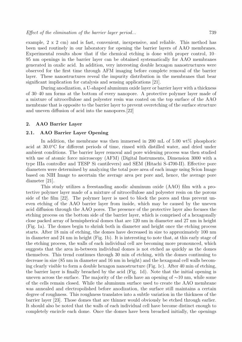
Fig. 2. AFM topography and phase images of the AAO membrane after(a and b) 70 min and (c and d) 90 min of etching
anion (Ox), C2O2−4 , and H2O to be mixed with the alumina within the barrier layer, leading
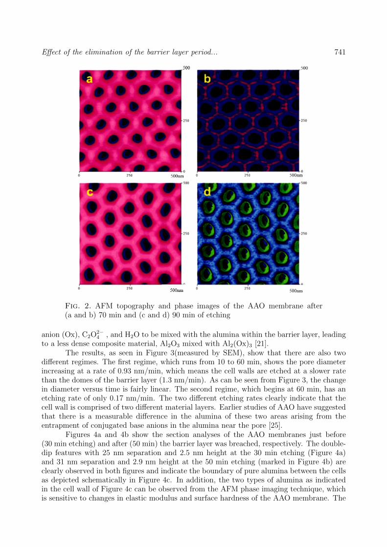
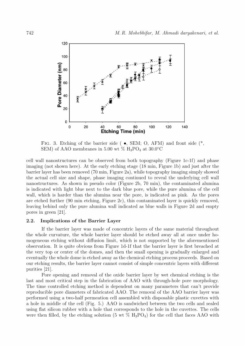
to a less dense composite material, Al2O3 mixed with Al2(Ox)3 [21].The results, as seen in Figure 3(measured by SEM), show that there are also two
different regimes. The first regime, which runs from 10 to 60 min, shows the pore diameterincreasing at a rate of 0.93 nm/min, which means the cell walls are etched at a slower ratethan the domes of the barrier layer (1.3 nm/min). As can be seen from Figure 3, the changein diameter versus time is fairly linear. The second regime, which begins at 60 min, has anetching rate of only 0.17 nm/min. The two different etching rates clearly indicate that thecell wall is comprised of two different material layers. Earlier studies of AAO have suggestedthat there is a measurable difference in the alumina of these two areas arising from theentrapment of conjugated base anions in the alumina near the pore [25].
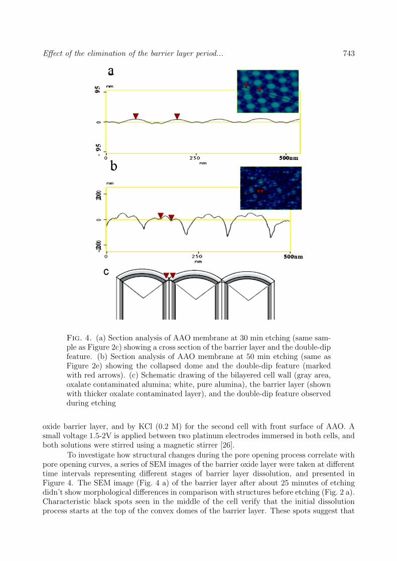
Figures 4a and 4b show the section analyses of the AAO membranes just before(30 min etching) and after (50 min) the barrier layer was breached, respectively. The double-dip features with 25 nm separation and 2.5 nm height at the 30 min etching (Figure 4a)and 31 nm separation and 2.9 nm height at the 50 min etching (marked in Figure 4b) areclearly observed in both figures and indicate the boundary of pure alumina between the cellsas depicted schematically in Figure 4c. In addition, the two types of alumina as indicatedin the cell wall of Figure 4c can be observed from the AFM phase imaging technique, whichis sensitive to changes in elastic modulus and surface hardness of the AAO membrane. The
742 M. R. Mohebbifar, M. Ahmadi daryakenari, et al.
Fig. 3. Etching of the barrier side ( •, SEM; O, AFM) and front side (*,SEM) of AAO membranes in 5.00 wt % H3PO4 at 30.0C
cell wall nanostructures can be observed from both topography (Figure 1c-1f) and phaseimaging (not shown here). At the early etching stage (18 min, Figure 1b) and just after thebarrier layer has been removed (70 min, Figure 2a), while topography imaging simply showedthe actual cell size and shape, phase imaging continued to reveal the underlying cell wallnanostructures. As shown in pseudo color (Figure 2b, 70 min), the contaminated aluminais indicated with light blue next to the dark blue pore, while the pure alumina of the cellwall, which is harder than the alumina near the pore, is indicated as pink. As the poresare etched further (90 min etching, Figure 2c), this contaminated layer is quickly removed,leaving behind only the pure alumina wall indicated as blue walls in Figure 2d and emptypores in green [21].
2.2. Implications of the Barrier Layer
If the barrier layer was made of concentric layers of the same material throughoutthe whole curvature, the whole barrier layer should be etched away all at once under ho-mogeneous etching without diffusion limit, which is not supported by the aforementionedobservation. It is quite obvious from Figure 1d-1f that the barrier layer is first breached atthe very top or center of the domes, and then the small opening is gradually enlarged andeventually the whole dome is etched away as the chemical etching process proceeds. Based onour etching results, the barrier layer cannot consist of simple concentric layers with differentpurities [21].
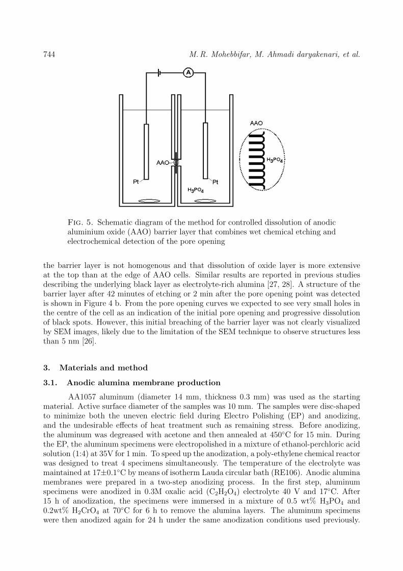
Pore opening and removal of the oxide barrier layer by wet chemical etching is thelast and most critical step in the fabrication of AAO with through-hole pore morphology.The time controlled etching method is dependent on many parameters that can’t providereproducible pore diameters of fabricated AAO. The removal of the AAO barrier layer wasperformed using a two-half permeation cell assembled with disposable plastic cuvettes witha hole in middle of the cell (Fig. 5.) AAO is sandwiched between the two cells and sealedusing flat silicon rubber with a hole that corresponds to the hole in the cuvettes. The cellswere then filled, by the etching solution (5 wt % H3PO4) for the cell that faces AAO with
Effect of the elimination of the barrier layer period... 743
Fig. 4. (a) Section analysis of AAO membrane at 30 min etching (same sam-ple as Figure 2c) showing a cross section of the barrier layer and the double-dipfeature. (b) Section analysis of AAO membrane at 50 min etching (same asFigure 2e) showing the collapsed dome and the double-dip feature (markedwith red arrows). (c) Schematic drawing of the bilayered cell wall (gray area,oxalate contaminated alumina; white, pure alumina), the barrier layer (shownwith thicker oxalate contaminated layer), and the double-dip feature observedduring etching
oxide barrier layer, and by KCl (0.2 M) for the second cell with front surface of AAO. Asmall voltage 1.5-2V is applied between two platinum electrodes immersed in both cells, andboth solutions were stirred using a magnetic stirrer [26].
To investigate how structural changes during the pore opening process correlate withpore opening curves, a series of SEM images of the barrier oxide layer were taken at differenttime intervals representing different stages of barrier layer dissolution, and presented inFigure 4. The SEM image (Fig. 4 a) of the barrier layer after about 25 minutes of etchingdidn’t show morphological differences in comparison with structures before etching (Fig. 2 a).Characteristic black spots seen in the middle of the cell verify that the initial dissolutionprocess starts at the top of the convex domes of the barrier layer. These spots suggest that
744 M. R. Mohebbifar, M. Ahmadi daryakenari, et al.
Fig. 5. Schematic diagram of the method for controlled dissolution of anodicaluminium oxide (AAO) barrier layer that combines wet chemical etching andelectrochemical detection of the pore opening
the barrier layer is not homogenous and that dissolution of oxide layer is more extensiveat the top than at the edge of AAO cells. Similar results are reported in previous studiesdescribing the underlying black layer as electrolyte-rich alumina [27, 28]. A structure of thebarrier layer after 42 minutes of etching or 2 min after the pore opening point was detectedis shown in Figure 4 b. From the pore opening curves we expected to see very small holes inthe centre of the cell as an indication of the initial pore opening and progressive dissolutionof black spots. However, this initial breaching of the barrier layer was not clearly visualizedby SEM images, likely due to the limitation of the SEM technique to observe structures lessthan 5 nm [26].
3. Materials and method
3.1. Anodic alumina membrane production
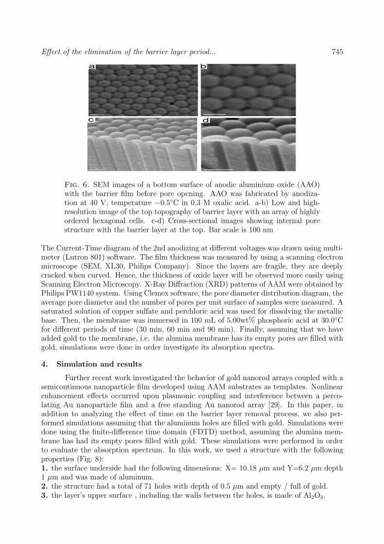
AA1057 aluminum (diameter 14 mm, thickness 0.3 mm) was used as the startingmaterial. Active surface diameter of the samples was 10 mm. The samples were disc-shapedto minimize both the uneven electric field during Electro Polishing (EP) and anodizing,and the undesirable effects of heat treatment such as remaining stress. Before anodizing,the aluminum was degreased with acetone and then annealed at 450C for 15 min. Duringthe EP, the aluminum specimens were electropolished in a mixture of ethanol-perchloric acidsolution (1:4) at 35V for 1 min. To speed up the anodization, a poly-ethylene chemical reactorwas designed to treat 4 specimens simultaneously. The temperature of the electrolyte wasmaintained at 17±0.1C by means of isotherm Lauda circular bath (RE106). Anodic aluminamembranes were prepared in a two-step anodizing process. In the first step, aluminumspecimens were anodized in 0.3M oxalic acid (C2H2O4) electrolyte 40 V and 17C. After15 h of anodization, the specimens were immersed in a mixture of 0.5 wt% H3PO4 and0.2wt% H2CrO4 at 70C for 6 h to remove the alumina layers. The aluminum specimenswere then anodized again for 24 h under the same anodization conditions used previously.
Effect of the elimination of the barrier layer period... 745
Fig. 6. SEM images of a bottom surface of anodic aluminium oxide (AAO)with the barrier film before pore opening. AAO was fabricated by anodiza-tion at 40 V, temperature −0.5C in 0.3 M oxalic acid. a-b) Low and high-resolution image of the top topography of barrier layer with an array of highlyordered hexagonal cells. c-d) Cross-sectional images showing internal porestructure with the barrier layer at the top. Bar scale is 100 nm
The Current-Time diagram of the 2nd anodizing at different voltages was drawn using multi-meter (Lutron 801) software. The film thickness was measured by using a scanning electronmicroscope (SEM, XL30, Philips Company). Since the layers are fragile, they are deeplycracked when curved. Hence, the thickness of oxide layer will be observed more easily usingScanning Electron Microscopy. X-Ray Diffraction (XRD) patterns of AAM were obtained byPhilips PW1140 system. Using Clemex software, the pore diameter distribution diagram, theaverage pore diameter and the number of pores per unit surface of samples were measured. Asaturated solution of copper sulfate and perchloric acid was used for dissolving the metallicbase. Then, the membrane was immersed in 100 mL of 5.00wt% phosphoric acid at 30.0Cfor different periods of time (30 min, 60 min and 90 min). Finally, assuming that we haveadded gold to the membrane, i.e. the alumina membrane has its empty pores are filled withgold, simulations were done in order investigate its absorption spectra.
4. Simulation and results
Further recent work investigated the behavior of gold nanorod arrays coupled with asemicontinuous nanoparticle film developed using AAM substrates as templates. Nonlinearenhancement effects occurred upon plasmonic coupling and interference between a perco-lating Au nanoparticle film and a free standing Au nanorod array [29]. In this paper, inaddition to analyzing the effect of time on the barrier layer removal process, we also per-formed simulations assuming that the aluminum holes are filled with gold. Simulations weredone using the finite-difference time domain (FDTD) method, assuming the alumina mem-brane has had its empty pores filled with gold. These simulations were performed in orderto evaluate the absorption spectrum. In this work, we used a structure with the followingproperties (Fig. 8):1. the surface underside had the following dimensions: X= 10.18 µm and Y=6.2 µm depth1 µm and was made of aluminum.2. the structure had a total of 71 holes with depth of 0.5 µm and empty / full of gold.3. the layer’s upper surface , including the walls between the holes, is made of Al2O3.
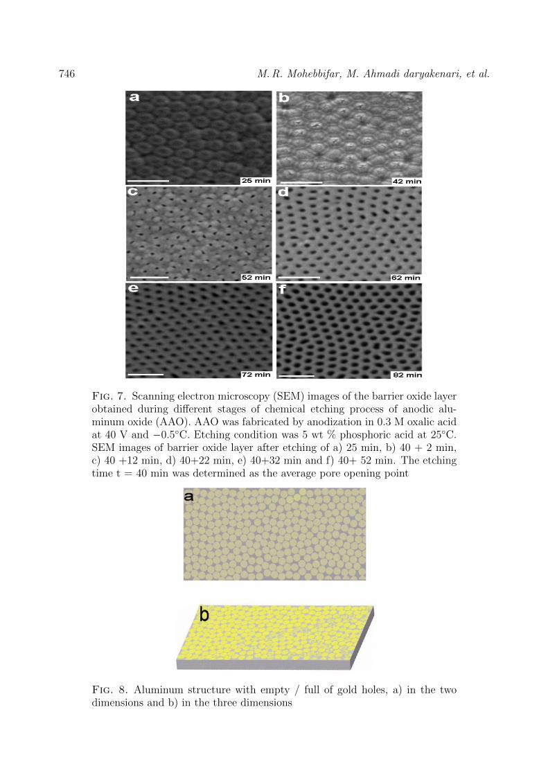
746 M. R. Mohebbifar, M. Ahmadi daryakenari, et al.
Fig. 7. Scanning electron microscopy (SEM) images of the barrier oxide layerobtained during different stages of chemical etching process of anodic alu-minum oxide (AAO). AAO was fabricated by anodization in 0.3 M oxalic acidat 40 V and −0.5C. Etching condition was 5 wt % phosphoric acid at 25C.SEM images of barrier oxide layer after etching of a) 25 min, b) 40 + 2 min,c) 40 +12 min, d) 40+22 min, e) 40+32 min and f) 40+ 52 min. The etchingtime t = 40 min was determined as the average pore opening point
Fig. 8. Aluminum structure with empty / full of gold holes, a) in the twodimensions and b) in the three dimensions
Effect of the elimination of the barrier layer period... 747
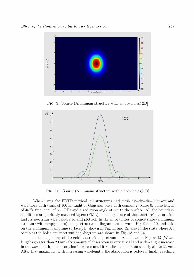
Fig. 9. Source (Aluminum structure with empty holes)[2D]
Fig. 10. Source (Aluminum structure with empty holes)[1D]
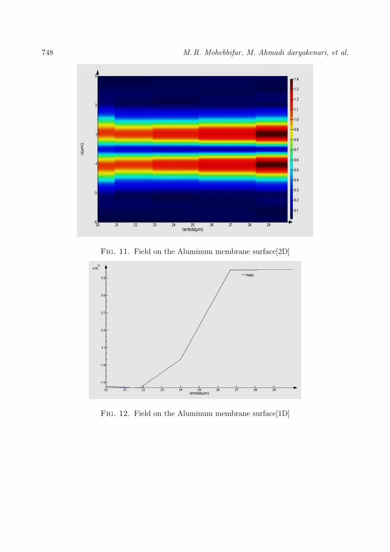
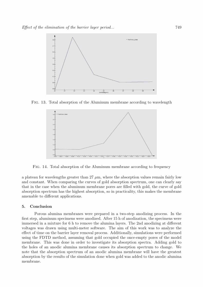
When using the FDTD method, all structures had mesh dx=dy=dz=0.05 µm andwere done with times of 100 fs. Light or Gaussian wave with domain 2, phase 0, pulse lengthof 45 fs, frequency of 650 THz and a radiation angle of 55 to the surface. All the boundaryconditions are perfectly matched layers (PML). The magnitude of the structure’s absorptionand its spectrum were calculated and plotted. In the empty holes or source state (aluminumstructure with empty holes), its spectrum and diagram are shown in Fig. 9 and 10, and fieldon the aluminum membrane surface[2D] shown in Fig. 11 and 12, also In the state where Auoccupies the holes, its spectrum and diagram are shown in Fig. 13 and 14.
In the beginning of the gold absorption spectrum curve, shown in Figure 13 (Wave-lengths greater than 20 µm) the amount of absorption is very trivial and with a slight increasein the wavelength, the absorption increases until it reaches a maximum slightly above 22 µm.After that maximum, with increasing wavelength, the absorption is reduced, finally reaching
748 M. R. Mohebbifar, M. Ahmadi daryakenari, et al.
Fig. 11. Field on the Aluminum membrane surface[2D]
Fig. 12. Field on the Aluminum membrane surface[1D]
Effect of the elimination of the barrier layer period... 749
Fig. 13. Total absorption of the Aluminum membrane according to wavelength
Fig. 14. Total absorption of the Aluminum membrane according to frequency
a plateau for wavelengths greater than 27 µm, where the absorption values remain fairly lowand constant. When comparing the curves of gold absorption spectrum, one can clearly saythat in the case when the aluminum membrane pores are filled with gold, the curve of goldabsorption spectrum has the highest absorption, so in practicality, this makes the membraneamenable to different applications.
5. Conclusion
Porous alumina membranes were prepared in a two-step anodizing process. In thefirst step, aluminum specimens were anodized. After 15 h of anodization, the specimens wereimmersed in a mixture for 6 h to remove the alumina layers. The 2nd anodizing at differentvoltages was drawn using multi-meter software. The aim of this work was to analyze theeffect of time on the barrier layer removal process. Additionally, simulations were performedusing the FDTD method, assuming that gold occupied the once-empty pores of the modelmembrane. This was done in order to investigate its absorption spectra. Adding gold tothe holes of an anodic alumina membrane causes its absorption spectrum to change. Wenote that the absorption spectrum of an anodic alumina membrane will have the greatestabsorption by the results of the simulation done when gold was added to the anodic aluminamembrane.
750 M. R. Mohebbifar, M. Ahmadi daryakenari, et al.
References
[1] F. Reidenbach, Surface Engineering, ASM International, Ohio, 124 p. (2007).[2] K. Itaya, S. Sugawara, K. Arai, and S. Saito. Properties of porous anodic aluminum oxide films as
membrances. Journal of Chemical Engineering of Japan, 17(6), P. 514–520 (1984).[3] H. Masuda, K. Yada and A. Osaka. Self-Ordering of Cell Configuration of Anodic Porous Alumina
with Large-Size Pores in Phosphoric Acid Solution. Japanese Journal of Applied Physics, 37(11A),P. 212–219 (1998).
[4] F. Keller, M.S. Hunter, D.L. Robinson, Structural Features of Oxide Coatings on Aluminum, TheElectrochemical Society, 1953, 100 (9), 411-419.
[5] D. Crouse, Y.H. Lo, A.E. Miller, M. Crouse. Self-ordered pore structure of anodized aluminum on siliconand pattern transfer. Appl. Phys. Lett., 76(1), P. 49–51 (2000).
[6] D.Qin , M.Lu , H.Li. Magnetic force microscopy of magnetic domain structure in highly ordered Conanowire arrays. Chem. Phys. Lett., 350(10), P. 51–56 (2001).
[7] T. Imai, S. Nomura. Quantum dot arrays prepared with self-organized nanopore and its photolumines-cence spectra. Physica E: Low-dimensional Systems and Nanostructures, 21(2), P. 1093–1097 (2004).
[8] M. Steinhart, R.B. Wehrspohn,U. Gosele, J. Wendorff. Nanotubes by Template Wetting: A ModularAssembly System. Chem. Int. Ed., 43(9), P. 1334–1344 (2004).
[9] J. Justin Gooding. Nanostructuring electrodes with carbon nanotubes: A review on electrochemistryand applications for sensing. Electrochim. Acta., 50(15), P. 3049–3060 (2005).
[10] D. Gong, V. Yadavalli, M. Paulose, M. Pishko, C. Grimes. Controlled molecular release using nanoporousalumina, Biomed. Microdevices., 5(1), P. 75–80 (2003).
[11] M. Darder, P. Aranda, M. Hernandez-Velez, E. Manova, E. Ruiz-Hitzky. Encapsulation of enzymes inalumina membranes of controlled pore size. Thin Solid Films., 495(8), P. 321–326 (2005).
[12] P. Bocchetta, R. Ferraro, F. Di Quarto. Advances in anodic alumina membranes thin film fuel cell:CsH2PO4 pore-filler as proton conductor at room temperature. Power Sources., 187(11), P. 49–56(2009).
[13] M. J. Zheng, L. D. Zhang, G. H. Li, W. Z. Shen. Fabrication and optical properties of large-scale uniformzinc oxide nanowire arrays by one-step electrochemical deposition technique. Chemical Physics Letters.,363(3), P. 123–128 (2002).
[14] W. Lee, R. Ji, U. Gosele, K. Nielsch. Fast fabrication of long-range ordered porous alumina membranesby hard anodization. Nature Materials, 5(6), P. 741–747 (2006).
[15] I. Vrubevsky, V. Parkoun, J. Schreckenbach, G. Marx. Study of porous oxide film growth on aluminumin oxalic acid using a re-anodizing technique. Applied Surface Science, 227(4), P. 282–292 (2004).
[16] H. Masuda, K. Yasui, Nishio. Fabrication of Ordered Arrays of Multiple Nanodots Using Anodic PorousAlumina as an Evaporation Mask. Advanced Materials., 12(14), P. 1031–1033 (2000).
[17] J. Liang, H. Chik, A. Yin, J.J. Xu. Two-dimensional lateral superlattices of nanostructures: Nonlitho-graphic formation by anodic membrane template. Appl. Phys., 91(12), P. 2544–2553 (2002).
[18] X. Mei, D. Kim, H. E. Ruda, Q. X. Guo. Molecular-beam epitaxial growth of GaAs and InGaAs/GaAsnanodot arrays using anodic Al2O3 nanohole array template masks. Appl. Phys. Lett., 81(11), P. 361–363 (2002).
[19] T. Xu, G. Zangari, R. M. Metzger. Periodic Holes with 10 nm Diameter Produced by Grazing Ar+Milling of the Barrier Layer in Hexagonally Ordered Nanoporous Alumina. Nano Lett., 2(1), P. 37–41(2002).
[20] H. Masuda and M. Satoh. Fabrication of Gold Nanodot Array Using Anodic Porous Alumina as anEvaporation Mask. J. Appl. Phys., 35(1), P. 126–129 (1996).
[21] Catherine Y. Han, Gerold A. Willing, Zhili Xiao, and H. Hau Wang. Control of the Anodic AluminumOxide Barrier Layer Opening Process by Wet Chemical Etching. Langmuir, 23(3), P. 1564–1568 (2007).
[22] T.T. Xu, R. Piner and R.S.Ruoff. An Improved Method to Strip Aluminum from Porous Anodic AluminaFilms. Langmuir, 19(5) P. 1443–1449 (2003).
[23] H. Masuda, A. Abe, M. Nakao, A. Yokoo, T. Tamamura, K. Nishio, Ordered Mosaic Nanocompositesin Anodic Porous Alumina. AdV. Mater., 15(2), P. 161–164 (2003).
[24] J. P. O’Sullivan and G. C. Wood. Proc. R. Soc. London, Ser. A. 317(2), P. 511–519 (1970).[25] G. E. Thompson, and G. C. Wood. Porous anodic film formation on aluminium. Nature, 290(9), P. 230–
232 (1981).

Effect of the elimination of the barrier layer period... 751
[26] Mickael Lillo, Dusan Losic. Pore opening detection for controlled dissolution of barrier oxide layerand fabrication of nanoporous alumina with through-hole morphology. Journal of Membrane Science.237(1), P. 11–17 (2008).
[27] C. Y. Han, G. A. Willing, Z. L. Xiao, H. H. Wang. Control of the anodic aluminum oxide barrier layeropening process by wet chemical etching. Langmuir, 23(3), P. 1564–1568 (2007).
[28] J. J. Schneider, N. Engstler, K. P. Budna, C. Teichert, S. Franzka, Freestanding, highly flexible, largearea, “nanoporous alumina membranes with complete through-hole pore morphology”. European Jour-nal of Inorganic Chemistry, 2005(12), P. 2352–2359 (2005).
[29] Zhou Z-K et al. Tuning gold nanorod-nanoparticle hybrids into plasmonic fano resonance for dramati-cally enhanced light emission and transmission. Nano Lett., 11(1), P. 49–55 (2011).
NANOSYSTEMS: PHYSICS, CHEMISTRY, MATHEMATICS, 2014, 5 (6), P. 752–756
X-RAY LUMINESCENCE OF BaF2:Ce3+ POWDERS
S. Kh. Batygov, M. N. Mayakova, S. V. Kuznetsov, P. P. Fedorov
A. M. Prokhorov General Physics Institute, Russian Academy of Sciences, Moscow, Russia
PACS 61.46
We studied the mechanism for the formation of cerium-activated barium fluoride scintillation ceramics and espe-
cially X-ray luminescence of its powdered precursors, prepared by co-precipitation of barium and cerium fluorides
from aqueous solutions. We have found that the Ce3+ luminescence, which is typical for cerium (III)-containing
ceramics and single crystals, was not observed for such polycrystalline precursors, and the intensity of barium
fluoride’s own luminescence decreases with increasing amounts of the cerium dopant in the specimens. We have
interpreted our results as two-phase precipitation of barium hydrofluoride (BaF2·HF) and cerium fluoride, respec-
tively. Cerium (III) became incorporated in fluorite-type barium fluoride lattice only later, in the course of ceramics
synthesis by the hot-pressing technique.
Keywords: Fluoride powder, nanoparticles, scintillators, X-ray luminescence.
Received: 30 October 2014
1. Introduction
The study of fluoride nanoceramics is one of the most promising areas of modernphotonics [1–3], and barium fluoride is one of the most interesting and actively studied fastscintillators [3–8]. BaF2 ceramics and single crystals exhibit two types of emission: a broadexcitonic line with maximum near 300 nm (slow luminescence, τ = 600 – 800 ns), and a short-wavelength line at 220 nm, corresponding to the superfast luminescence core-valence transitions(τ = 0.8 ns). Addition of CeF3 to the BaF2 matrix leads to the transfer of exciton energy tocerium ion and powerful Ce3+-luminescence at 300 – 350 nm [7, 9–12]. Because BaF2:Ce3+
ceramics have an enhanced scintillation yield compared to the same composition single crys-tals [11, 12], we have developed a technology for the further improvement of its optical qualitythat included precipitation of barium hydrofluoride BaF2·HF from aqueous solutions followedby its thermal decomposition with HF evolution. The latter has been found to be an active flu-orinating reagent that eliminated oxygen impurities from the batch materials [13, 14]. Thus, thetopic of the present paper concerns the influence of cerium doping on the synthesis of bariumfluoride scintillation ceramics and its precursors.
2. Experimental
99.99 wt. % pure Ba(NO3)2, Ce(NO3)3, HF and doubly-distilled water were usedas starting materials. All precipitation experiments were carried in polypropylene reactors atroom temperature under air. All samples were prepared by co-precipitation from aqueoussolutions [13–15]. Premixed corresponding amounts of starting 0.17 M metal nitrate solutions(Ce/(Ce+Ba) (molar ratios varied from 0.01 to 1%) were treated in a dropwise manner withconcentrated aqueous HF under vigorous stirring. The HF content in the formed matrix solutionwas maintained at about 47 vol. %. Formed precipitates were additionally treated with conc.HF, decanted, thoroughly washed with doubly-distilled water and dried under air at 40 C.
X-Ray luminescence of BaF2:Ce3+ powders 753
Further thermal treatment included heating of the synthesized precipitates at 10 C/min to550 C followed by 1-hour annealing at the same (550 C) temperature under air.
The phase composition of the synthesized samples was determined by X-ray diffractionanalysis (Bruker D8 diffractometer, CuKα radiation, TOPAS software for lattice parametercalculations and profile treatment of the X-ray diffraction pattern lines). All sample X-ray-initiated luminescence spectra were recorded at room temperature (KSVU spectrometer, Cuanode, 10 kV , 10 mA ).
3. Results and discussion
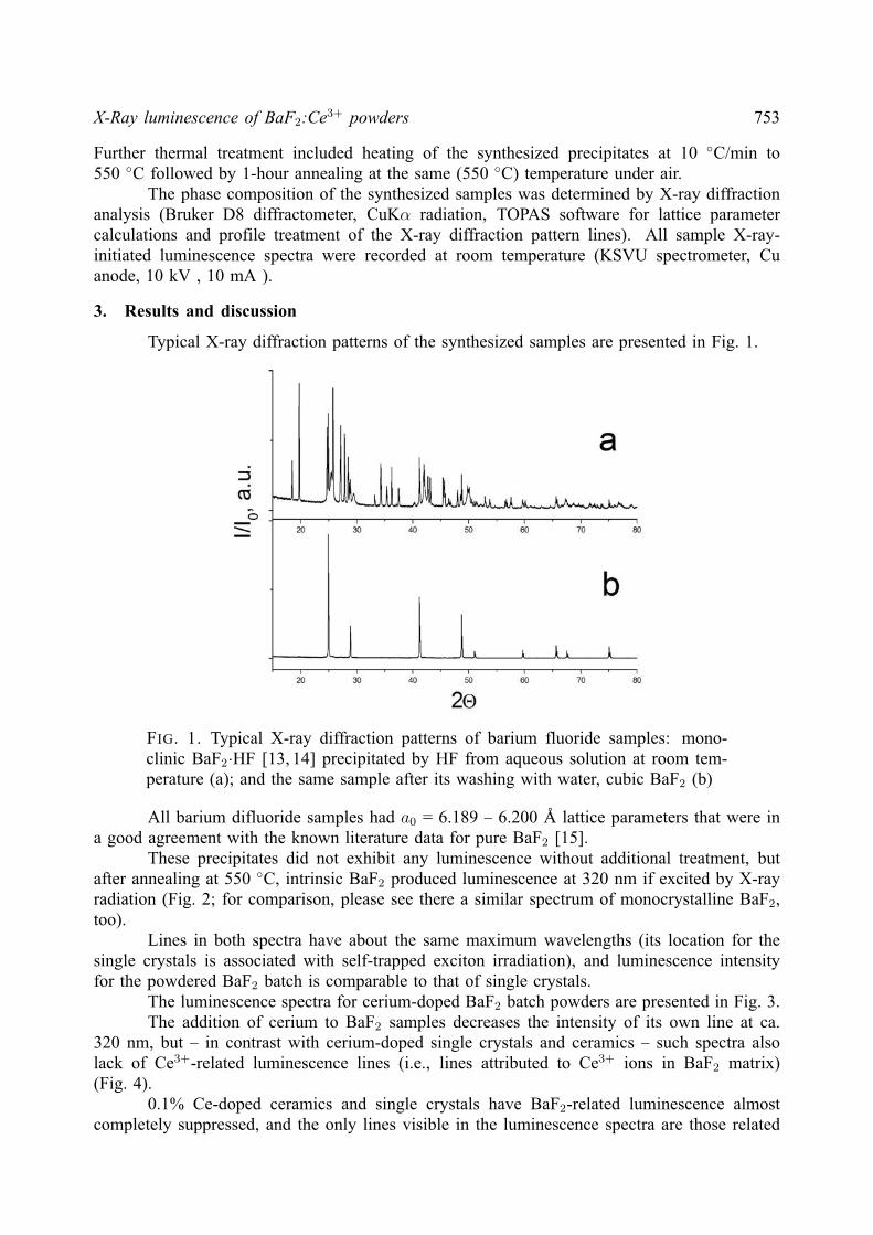
Typical X-ray diffraction patterns of the synthesized samples are presented in Fig. 1.
FIG. 1. Typical X-ray diffraction patterns of barium fluoride samples: mono-clinic BaF2·HF [13, 14] precipitated by HF from aqueous solution at room tem-perature (a); and the same sample after its washing with water, cubic BaF2 (b)
All barium difluoride samples had a0 = 6.189 – 6.200 A lattice parameters that were ina good agreement with the known literature data for pure BaF2 [15].
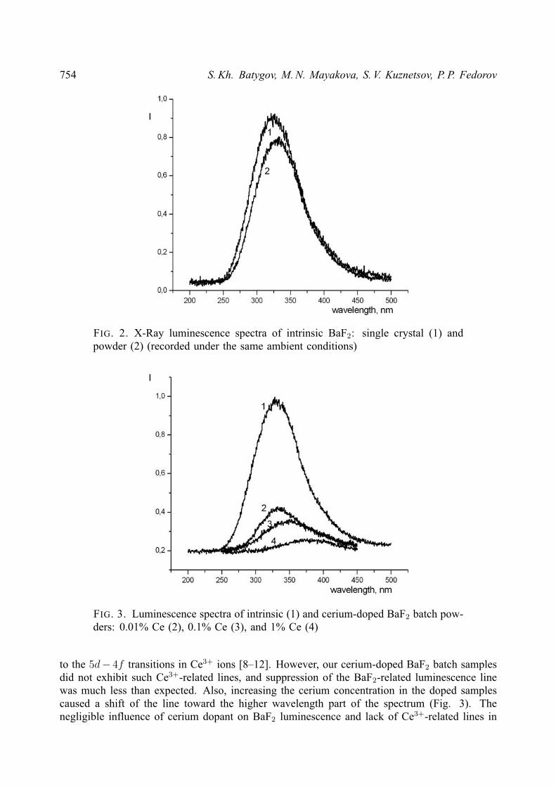
These precipitates did not exhibit any luminescence without additional treatment, butafter annealing at 550 C, intrinsic BaF2 produced luminescence at 320 nm if excited by X-rayradiation (Fig. 2; for comparison, please see there a similar spectrum of monocrystalline BaF2,too).
Lines in both spectra have about the same maximum wavelengths (its location for thesingle crystals is associated with self-trapped exciton irradiation), and luminescence intensityfor the powdered BaF2 batch is comparable to that of single crystals.
The luminescence spectra for cerium-doped BaF2 batch powders are presented in Fig. 3.The addition of cerium to BaF2 samples decreases the intensity of its own line at ca.
320 nm, but – in contrast with cerium-doped single crystals and ceramics – such spectra alsolack of Ce3+-related luminescence lines (i.e., lines attributed to Ce3+ ions in BaF2 matrix)(Fig. 4).
0.1% Ce-doped ceramics and single crystals have BaF2-related luminescence almostcompletely suppressed, and the only lines visible in the luminescence spectra are those related
754 S. Kh. Batygov, M. N. Mayakova, S. V. Kuznetsov, P. P. Fedorov
FIG. 2. X-Ray luminescence spectra of intrinsic BaF2: single crystal (1) andpowder (2) (recorded under the same ambient conditions)
FIG. 3. Luminescence spectra of intrinsic (1) and cerium-doped BaF2 batch pow-ders: 0.01% Ce (2), 0.1% Ce (3), and 1% Ce (4)
to the 5d− 4f transitions in Ce3+ ions [8–12]. However, our cerium-doped BaF2 batch samplesdid not exhibit such Ce3+-related lines, and suppression of the BaF2-related luminescence linewas much less than expected. Also, increasing the cerium concentration in the doped samplescaused a shift of the line toward the higher wavelength part of the spectrum (Fig. 3). Thenegligible influence of cerium dopant on BaF2 luminescence and lack of Ce3+-related lines in
X-Ray luminescence of BaF2:Ce3+ powders 755
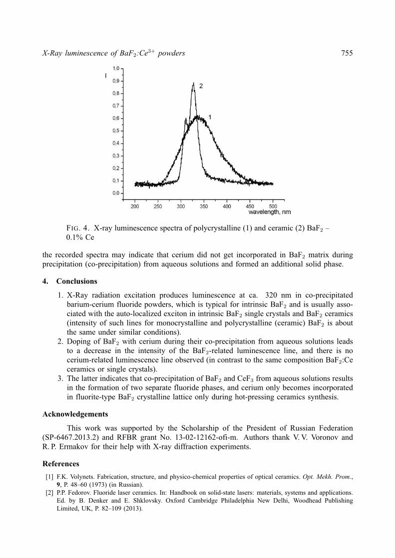
FIG. 4. X-ray luminescence spectra of polycrystalline (1) and ceramic (2) BaF2 –0.1% Ce
the recorded spectra may indicate that cerium did not get incorporated in BaF2 matrix duringprecipitation (co-precipitation) from aqueous solutions and formed an additional solid phase.
4. Conclusions
1. X-Ray radiation excitation produces luminescence at ca. 320 nm in co-precipitatedbarium-cerium fluoride powders, which is typical for intrinsic BaF2 and is usually asso-ciated with the auto-localized exciton in intrinsic BaF2 single crystals and BaF2 ceramics(intensity of such lines for monocrystalline and polycrystalline (ceramic) BaF2 is aboutthe same under similar conditions).
2. Doping of BaF2 with cerium during their co-precipitation from aqueous solutions leadsto a decrease in the intensity of the BaF2-related luminescence line, and there is nocerium-related luminescence line observed (in contrast to the same composition BaF2:Ceceramics or single crystals).
3. The latter indicates that co-precipitation of BaF2 and CeF3 from aqueous solutions resultsin the formation of two separate fluoride phases, and cerium only becomes incorporatedin fluorite-type BaF2 crystalline lattice only during hot-pressing ceramics synthesis.
Acknowledgements
This work was supported by the Scholarship of the President of Russian Federation(SP-6467.2013.2) and RFBR grant No. 13-02-12162-ofi-m. Authors thank V. V. Voronov andR. P. Ermakov for their help with X-ray diffraction experiments.
References
[1] F.K. Volynets. Fabrication, structure, and physico-chemical properties of optical ceramics. Opt. Mekh. Prom.,9, P. 48–60 (1973) (in Russian).
[2] P.P. Fedorov. Fluoride laser ceramics. In: Handbook on solid-state lasers: materials, systems and applications.Ed. by B. Denker and E. Shklovsky. Oxford Cambridge Philadelphia New Delhi, Woodhead PublishingLimited, UK, P. 82–109 (2013).
756 S. Kh. Batygov, M. N. Mayakova, S. V. Kuznetsov, P. P. Fedorov
[3] P.P. Fedorov, S.V. Kuznetsov, et al. Microstructure and scintillation characteristics of BaF2 ceramics. InorganicMaterials, 50 (7), P. 738–744 (2014).
[4] P. Schotanus, P. Dorenbos, C.W.E. van Eijk, R.W. Hollander. Recent development in scintillator research.IEEE Trans. Nucl. Sci., 36 (1), P. 132–136 (1989).
[5] M. Laval, M. Moszynaki, R. Allemand. Barium fluoride-inorganic scintillator for subnanosecond timing. Nucl.Instrum. Methods, 206 (1), P. 169–176 (1983).
[6] P.A. Rodnyi. Core-valence transitions in wide-band-gap ionic crystals. Phys. Solid State, 34 (7), P. 1975–1998(1992).
[7] B.P. Sobolev. Multicomponent crystals based on heavy metal fluorides for radiation detectors. Barcelona:Inst. d’Estudis Catalans (1994).
[8] D.M. Seliverstov, A.A. Demidenko, et al. New fast scintillators on the base of BaF2 crystals with increasedlight yield of 0.9 ns luminescence for TOF PET. Nuclear Instruments and Methods in Physics Research A,695, P. 369–372 (2012).
[9] P. Schotanus, P. Dorenbos, C.W.E. van Eijk, and R.W. Hollander. Recent development in scintillator research.IEEE Trans. Nucl. Sci., 36 (1), P. 132–136 (1989).
[10] A.J. Wojtowicz, P. Szupryczynski, et al., Radioluminescence and recombination processes in BaF2:Ce.J. Phys.: Condens. Matter, 12, P. 4097–4124 (2000).
[11] Kh.S. Batygov, L.S. Bolyasnikova, et al. BaF2:Ce3+ scintillation ceramics. Doklady Physics, 53 (9), P. 485–488 (2008).
[12] P.A. Rodnyi, S.D. Gain, et al. Spectral-kinetic characteristics of crystals and nanoceramics based on BaF2 andBaF2:Ce. Phys. Solid State, 52 (9), P. 1910–1914 (2010).
[13] A.A. Luginina, P.P. Fedorov, et al. Synthesis of BaF2·HF and BaF2 from nitric solutions. Nanosystems:Physics, Chemistry, Mathematics, 3 (5), P. 125–137 (2012) (in Russsian).
[14] A.A. Luginina, A.E. Baranchikov, A.I. Popov, P.P. Fedorov. Preparation of barium monohydrofluorideBaF2·HF from nitrate aqueous solutions. Mater. Res. Bull., 49 (1), P. 199–205 (2014).
[15] P.P. Fedorov, M.N. Mayakova, et al. Co-Precipitation of Yttrium and Barium Fluorides from Aqueous Solu-tions. Mater. Res. Bull., 47, P. 1794–1799 (2012).
NANOSYSTEMS: PHYSICS, CHEMISTRY, MATHEMATICS, 2014, 5 (6), P. 757–781
NAVIGATION ON THE ENERGY SURFACEOF THE NONCOLLINEAR
ALEXANDER-ANDERSON MODEL
P. F. Bessarab1,2, A. Skorodumov3, V. M. Uzdin2,3, H. Jonsson4,5
1 Royal Institute of Technology KTH, Stockholm, Sweden2 St. Petersburg State University, St. Petersburg, Russia
3 ITMO University, St. Petersburg, Russia4 University of Iceland, Reykjavık, Iceland
5 Aalto University, Espoo, Finland
[email protected], [email protected], v [email protected], [email protected]
PACS 05.20.Dd, 75.10.-b
Implementation of the multiple impurity, noncollinear Alexander-Anderson model is described in detail and an
analytical expression given for the force which determines the orientation of the magnetic momenta as well as a
corresponding magnetic force theorem. Applications to trimers of Cr, Mn and Fe adsorbed on a metal surface are
described, including the energy surface as a function of the the angles specifying the orientation of the magnetic
momenta and minimum energy paths for transitions between stable states, which necessarily involve noncollinear
ordering. A simple model for the interaction of a magnetic STM tip with a Cr dimer on a surface is briefly
described. A finite range approximation is also formulated, which simplifies the self-consistency calculations
and results in linear scaling of the computational effort with the number of magnetic atoms in the system. The
theoretical approach described here can be used to study magnetic systems with complex energy landscapes,
including stable states and magnetic transitions in frustrated magnetic systems, over a range in length scale, from
a few to several thousands of magnetic atoms.
Keywords: itinerant magnetism, Alexander-Anderson model, magnetic force theorem, noncollinear ordering, en-
ergy surface, minimum energy path.
Received: 7 November 2014
Revised: 15 November 2014
1. Introduction
Noncollinear magnetic states are of great importance, not only because the stable statesof many systems are noncollinear, as has been demonstrated in recent experimental measure-ments of nano-scale islands [1] and thin layers [2,3], but also because magnetic systems drivenout of equilibrium by some external perturbation such as a magnetic field, spin-polarized cur-rent or thermal fluctuation, as well as spin dynamics at finite temperature necessarily involveconfigurations where the magnetic momenta can be far from parallel to each other. In particular,a proper description of non-stationary, noncollinear magnetic states is important in studies ofthermally activated magnetic transitions. Within harmonic transition state theory (TST) [4], min-imum energy paths (MEPs) in a configuration space connecting stable states have to be found.Following an MEP means rotating the magnetic momenta in an optimal way so as to minimizethe energy with respect to all degrees of freedom perpendicular to the path. Of particular im-portance for estimating the rate are the maxima along the path which correspond to first ordersaddle points on the energy surface. These define the activation energy for transitions between
758 P. F. Bessarab, A. Skorodumov, V. M. Uzdin, H. Jonsson
stable magnetic states and give the temperature dependence of the transition rate. Being a pathof maximal statistical weight, an MEP also gives a detailed description of the optimal transitionmechanism. Even if the stable states of the system are collinear, the configurations along theMEP can be noncollinear, representing complex, non-uniform rotations of the spins [5–7].
The basic physical quantity from which most magnetic properties of an electronic systemcan be derived is the electron density, which becomes a 2 × 2 matrix in a noncollinear, spin-polarized theory:
ρ(~r) =
(ρ++(~r) ρ+−(~r)
ρ−+(~r) ρ−−(~r)
), (1)
where + and − denote the spin projections. The sum of the diagonal elements of ρ(~r) gives thecharge density while their difference gives the projection of the spin density on the quantizationaxis. The off-diagonal elements of the matrix (1) determine in quasi-classical framework thecomponents of the magnetization density perpendicular to the quantization axis. In general, atany point in space, the expectation value of magnetization density can be calculated from
~m(~r) = Trs [~σρ(~r)] . (2)
Here, ~σ = (σx, σy, σz) are the Pauli matrices and Trs means the trace operation in spin space. Acontinuous vector field of magnetization density can be calculated using, for example, densityfunctional theory (DFT) [8–10], for many important magnetic materials including 3d-transitionmetals and rare-earth magnets. But, in most cases, the magnetization density is highly localizedon atomic sites. An atomic moment approximation can then be used where the orientationof the magnetization within a region surrounding each atom is considered to be fixed and themagnetization density is assumed to be zero in the interstitial regions between the atomic sites.A magnetic configuration is then defined by a set of magnetic momentum vectors, one vectorassociated with each of the magnetic atoms.
A further approximation can be made based on the hierarchy of relaxation times. Therelaxation of charge and magnitude of the magnetic moments is assumed to be much faster thanthe relaxation of the orientation of the magnetic vectors [11]. The fast degrees of freedom,charge and magnitude of magnetic moments, are assumed to adjust instantaneously to changesin the slow degrees of freedom, the direction of the magnetic moments as defined by polar andazimuthal angles θ and φ. The magnetic properties of a system, including the total energy,are then completely characterized by the slow degrees of freedom only. This is analogous tothe Born-Oppenheimer approximation in atomic systems where the fast degrees of freedom areassociated with the electrons while the positions of the nuclei are the slowly varying degrees offreedom.
Within the atomic moment and adiabatic approximations, spin dynamics simulations aswell as iterative searches for stable magnetic states and MEPs between them can be viewed asnavigation on the systems energy surface as a function of the angles defining the orientationof the magnetic moments. Efficient navigation requires efficient evaluation of not only theenergy but also the changes in energy with orientation, that is the ‘forces’, or ‘torques’ actingon the magnetic moments. The energy surface can in principle be characterized within thetight-binding approach [12] and DFT [13,14]. Such calculations are, however, complicated andcomputationally intensive. In order to describe nonstationary magnetic states, local constrainingfields are needed to orient the magnetic vectors in the predefined orientations [15]. These localfields are not known a priori, so an additional iterative cycle needs to be added to the self-consistency procedure to find them. As a result, the calculation of an arbitrary, nonstationary,noncollinear state in a system of several non-equivalent magnetic moments is a challenging taskwithin DFT and tight-binding methods.
Navigation on the energy surface of the noncollinear Alexander-Anderson model 759
In most cases, the evolution of extended magnetic systems is described using simple,phenomenological models, in particular Heisenberg-type models, where the total energy andgradients of the energy can be obtained analytically. However, in order to describe magneticsystems accurately enough, the model Hamiltonian may need to include several phenomenolog-ical terms. In addition to the usual magnetic exchange, anisotropy and dipole-dipole interaction,more elaborate interactions, such as biquadratic exchange and Dzyaloshinsky-Moriya interac-tion have been invoked to reproduce experimental observations accurately enough [2]. Themagnitude of the magnetic moments and interaction parameters in such Heisenberg-type modelsare typically kept unchanged as the magnetic vectors rotate. This approach can be accurateenough for small deviations from collinear stable states, but is expected to fail for large rota-tion angles in itinerant electron systems [16] where the magnitude of the magnetic momentsand coupling parameters depend on the relative orientation of the moments. While additionalparameters and elaborate expressions for the dependence of the parameters on the orientation ofthe magnetic moments can, in principle, be used to make a Heisenberg-type model reproduceany magnetic system, the transferability of the parameter values obtained in this way may bequite limited. Models that better describe the underlying physics and rely on only a few, welldefined parameters are then preferable.
The Alexander-Anderson (AA) model [17, 18] describes the interaction of magnetic im-purities in a system containing itinerant electrons. It includes two electronic bands: a quasilocal-ized band of d-electrons and a band of itinerant s(p)-electrons. A noncollinear extension of theAA model (NCAA) has been developed within mean-field approximation as well as an efficientimplementation of the self-consistency calculations for an arbitrary number of non-equivalentmagnetic impurities using the recursive Green function method [19, 20] and analytical trans-formations of the density of states [21–23]. The NCAA model can be applied to large andcomplex magnetic systems where a self-consistent calculation of the number of d-electrons andmagnitude of the magnetic moments is carried out for a given orientation. For an arbitrary,stationary or non-stationary orientation, only the number of d-electrons and magnitude of themagnetic moments are modified during the self-consistency calculations. The orientation ofthe magnetic vectors remains unaffected, i.e. in the NCAA model, changes in orientation arecompletely decoupled from the self-consistency procedure. This is different from DFT calcu-lations, where the orientation of the magnetic moments at a non-stationary point is modifiedduring self-consistency calculations unless local constraining fields fixing the orientation of themagnetic moments to the predefined direction are included [15].
In our recent paper [23], a magnetic force theorem for the NCAA model has been derivedwhich makes it possible to calculate the energy gradient without repeated self-consistencycalculations and also provides analytic expression for the force acting on the orientation ofthe magnetic moments. This theorem is particularly important for large scale simulation ofdynamics, calcualtion of minimum energy paths, or, in general, navigation on the energy surfaceof a magnetic system.
The NCAA model, however, does not describe the band structure of an itinerant mag-net in detail. Similar to the Heisenberg-type models, the NCAA model only focuses on theenergetics due to magnetic interactions. But, unlike Heisenberg-type models, the NCAA modelcorrectly accounts for the itinerant nature of 3d-transition metal systems: both the magnitudeof the magnetic moments and the interatomic exchange parameters (analogous to exchangeparameters in a Heisenberg Hamiltonian), are predicted to vary upon rotation of the magneticmomentum vectors. The NCAA model has, for example, been used successfully to describe

760 P. F. Bessarab, A. Skorodumov, V. M. Uzdin, H. Jonsson
magnetism of 3d-metal surfaces and interfaces [22]. Moreover, a noncollinear ordering of mag-netic moments in nanoclusters of 3d-metal atoms was obtained in calculations using the NCAAmodel [24–26], and this prediction was later confirmed by DFT calculations [27, 28].
This article is organized as follows. In the following section, the NCAA model isdescribed as well as the method used in the self-consistency calculations. In Sec. III, themagnetic force theorem is presented and an expression given for the magnetic force. In Sec. IV,the method is applied to magnetic trimers and to a simple model of a magnetic tip of a scanningtunneling microscope (STM) interacting with a dimer adsorbed on a metal surface. In Sec. V,the finite range approximation is discussed as well as an application to Fe-atoms adsorbed on aW(110) surface, as both a full monolayer and a large island. Section VI gives a summary.
2. Noncollinear Alexander-Anderson model
The AA model [18] extended to multiple-impurities and noncollinear magnetic orderinghas been described elsewhere [21, 24]. However, we present here a comprehensive descriptionof the model and its implementation for completeness.
The electronic structure of a 3d transition metal system is approximated by an itinerants(p)-electron band and five degenerate, quasi-localized d-orbitals. The Hamiltonian is as follows:
H =∑k,α
εknkα +∑i,α
ε0iniα +∑k,i,α
(υikd
†iαckα + υkic
†kαdiα
)+∑i6=j,α
υijd†iαdjα +
1
2
∑i,α
Uiniαni−α,(3)
where only one of the five d-orbitals is considered explicitly. Here, d†iα(diα) and c†kα(ckα) arecreation (annihilation) operators for d-electrons localized on atom i and itinerant s(p)-electronswith the wave vector k, respectively; niα = d†iαdiα, nkα = c†kαckα are the correspondingoccupation number operators. Greek indices denote spin projection (α, β = ±). The energy ofnon-interacting s(p) electrons, εk, and d-electrons, ε0i , hybridization parameters, υik, hoppingparameters, υij , and Coulomb repulsion between electrons with opposite spin projection, Ui,are spin independent. The last term in the Hamiltonian, Uiniαni−α, describes the interactionbetween d-electrons localized on atom i.
This Hamiltonian is invariant with respect to the choice of quantization axis. In orderto describe noncollinear magnetic states, a mean field approximation is invoked at each site ifor the d-electron operators, d†iα and diα, where the quantization axis, zi, is chosen to be alongthe local magnetic moment associated with atom i. The last term in Eqn.(3) is transformedaccording to
niαni−α ≈ niα〈ni−α〉+ 〈niα〉ni−α − 〈niα〉〈ni−α〉. (4)
Operators with a tilde correspond to a local reference frame associated with the quantizationaxis zi and angular parentheses denote expectation values of operators. The last term in Eqn. (4)represents the double counting term. The mean-field Hamiltonian is rewritten in terms of d†iαand diα whose quantization axis is the laboratory z axis, the same for all sites i. Creation(annihilation) operators are transformed using the spin-1
2rotation matrix [29]:(
di+di−
)= U
(di+di−
), (5)
Navigation on the energy surface of the noncollinear Alexander-Anderson model 761
where U is given by:
U =
(exp (iφi/2) cos (θi/2) exp (−iφi/2) sin (θi/2)
− exp (iφi/2) sin (θi/2) exp (−iφi/2) cos (θi/2)
). (6)
Here, the polar angle θi and the azimuthal angle φi define the direction of ith magnetic momentwith respect to the laboratory quantization axis z. After performing the operations (4) and (5)for each site i, the mean-field Hamiltonian is given by:
HMF =∑k,α
εknkα +∑i,α
εαi niα +∑k,i,α
(υikd
†iαckα + υkic
†kαdiα
)+∑i,j,α,β
υαβij d†iαdjβ −
1
4
∑i
Ui(N2i −M2
i
),
(7)
where
εαi = ε0i +Ui2
(Ni − α cos θiMi) , (8)
υαβij =Ui2
(δαβ − 1
)δij exp (−αiφi) sin θiMi + (1− δij) δαβυij. (9)
The number of d-electrons, Ni, and the magnitude of the magnetic moments, Mi, in Eqs. (7)-(9)are defined in terms of the expectation value of occupation number operators:
Ni = 〈d†i+di+〉+ 〈d†i−di−〉 = 〈ni+〉+ 〈ni−〉, (10)
Mi = 〈d†i+di+〉 − 〈d†i−di−〉 = 〈ni+〉 − 〈ni−〉. (11)
In this model, the magnetic structure of a system consisting of P 3d-metal atomssupported on a metallic substrate is described by a set of values of Ni and Mi, i = 1, . . . , P ,which need to be found from self-consistency iterations for any given orientation of the magneticmoments. The number of d-electrons, Ni, and the magnitude of the magnetic moments, Mi, canbe obtained from the Green’s function, G(ε − is) = [ε− is−HMF ]−1, s = +0. Equations forthe matrix elements of the Green function are derived from
(E−HMF )G(E) = I, (12)
whereE = ε− is. (13)
This gives the following:
(E− εk)Gαβki (E)−∑l
υklGαβli (E) = 0, (14)
(E− εαi )Gαβij (E)−∑l,γ
υαγil Gγβlj (E)−
∑k
υikGαβkj (E) = δijδ
αβ. (15)
By substituting the matrix elements Gαβki (E) derived from Eqn. (14) into Eqn. (15), an equation
for the matrix elements of the d-electron Green function can be obtained as:(E− εαi −
∑k
υikυkiE− εk
)Gαβij (E)−
∑l 6=i
(υil +
∑k
υikυklE− εk
)Gαβlj (E)
+∑γ
υαγii Gγβij (E) = δijδ
αβ.
(16)
The magnetism of 3d-transition metal systems is mostly determined by the d-electrons.Therefore, only the Green function for d-electrons, G(E) ≡ G(d)(E), will be considered explicitly
762 P. F. Bessarab, A. Skorodumov, V. M. Uzdin, H. Jonsson
in what follows. According to Eqn. (16), G(E) is a resolvent of an effective, mean fieldHamiltonian for the d-electrons, H ≡ H
(d)MF , with parameters that are renormalized due to the
influence of the itinerant s(p)-electrons. This Hamiltonian is given by:
H =∑i,α
Eαi niα +
∑i,j,α,β
V αβij d
†iαdjβ −
1
4
∑i
Ui(N2i −M2
i
), (17)
where
Eαi = E0
i +Ui2
(Ni − α cos θiMi) , (18)
V αβij =
Ui2
(δαβ − 1
)δij exp (−αiφi) sin θiMi + (1− δij) δαβVij. (19)
Here, E0i is a renormalized energy of unperturbed d-states:
E0i ≡ ε0i + Re
∑k
υikυkiE− εk
, (20)
which now acquires non-zero width due to the s(p)-d hybridization and the width parameter, Γ,is given by
Γ ≡ Im∑k
υikυkiE− εk
. (21)
Γ is included in the argument of the Green function when computing the density of states [17].The Vij are referred to as hopping parameters. They represent both a direct exchange betweend-states localized on sites i and j and as well as a contribution from indirect d-s(p)-d couplingthrough the conduction band
Vij ≡ υij +∑k
υikυkjE− εk
. (22)
Following [18], it is assumed that the on-site s(p)-d coupling is stronger than d-s(p)-d interactionof d-electrons at different sites and, hence, the imaginary part of Vij is neglected. E0
i , Ui, Vijand Γ are assumed to be constant parameters for the model. The choice of values for E0
i andUi depends mainly on the type of atom i, while the hopping parameters Vij also depend on thegeometry of the system, in particular the distance between atoms i and j.
The number of d-electrons, Ni, and the magnitude of the magnetic moments,Mi, definedin Eqs. (10) and (11), are expressed in terms of the Green function in the local frame ofreference, G(E), using the following standard relations:
Ni =1
π
0∫−∞
dε Im Tr Gii(ε− iΓ), (23)
Mi =1
π
0∫−∞
dε Im Tr[σzGii(ε− iΓ)
]. (24)
Here, Gii(ε − iΓ) is a 2×2 matrix with elements Gαβii (ε − iΓ) and σz is the z component of
the Pauli spin matrix. It is assumed that the magnetic system is in contact with a bath ofs(p)-electrons which fixes the Fermi level. The zero of energy is set to be at the Fermi level(εF = 0).
Navigation on the energy surface of the noncollinear Alexander-Anderson model 763
In order to be able to use Eqs. (23) and (24) in self-consistency calculations, the Greenfunction has to be transformed from the local reference frame to a global one using the spin-1
2rotation matrix U, Eq. (6):
G(E) = UG(E)U†. (25)
By substituting this relation into Eqs. (23) and (24), one obtains the following:
Ni =1
π
0∫−∞
dε Im[G++ii (ε− iΓ) +G−−ii (ε− iΓ)
], (26)
Mi =1
π
0∫−∞
dε Im[G++ii (ε− iΓ)−G−−ii (ε− iΓ)
]cos θi
+1
π
0∫−∞
dε Im[G+−ii (ε− iΓ)eiφi +G−+ii (ε− iΓ)e−iφi
]sin θi.
(27)
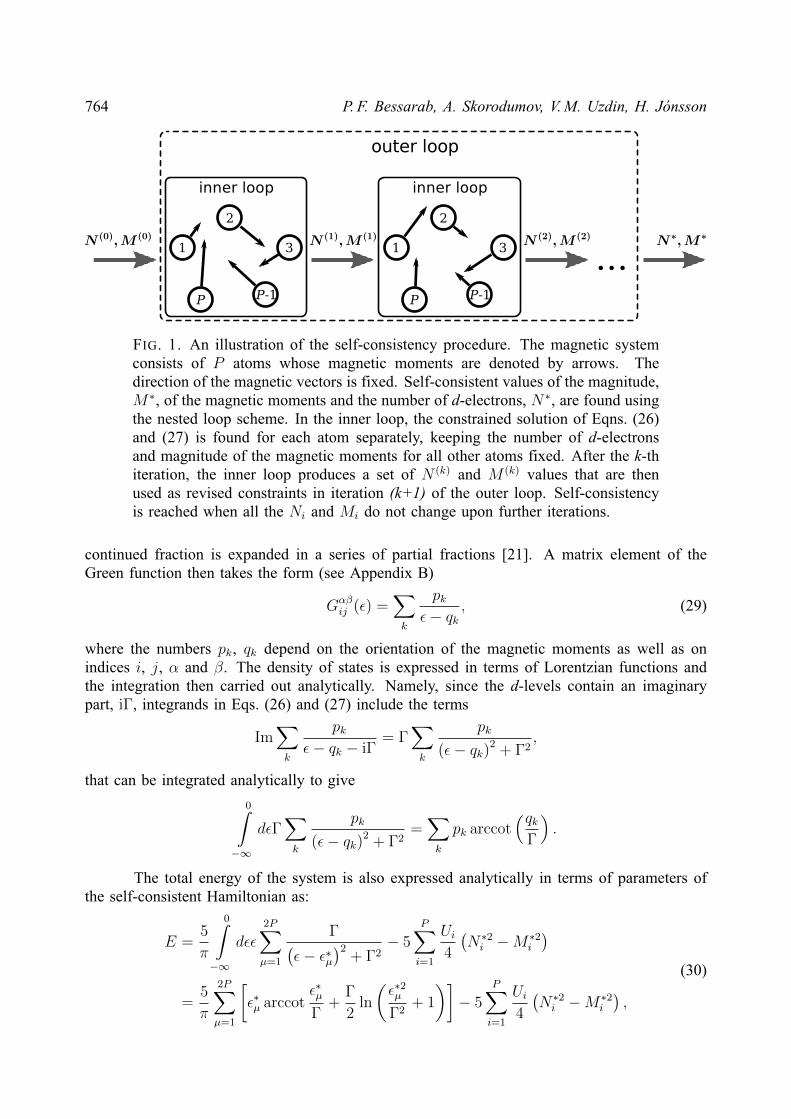
Since the matrix elements of the Green function depend on N and M , Eqns. (26)and (27) should be solved self-consistently for a given orientation of the magnetic vectorsstarting from some initial estimate for the number of d-electrons and magnitude of the magneticmoments. If the system consists of more than one atom, the self-consistency procedure containstwo nested loops. The inner loop involves finding the constrained solution of Eqns. (26) and (27)for each individual atom, while the number of d-electrons and magnitude of magnetic momentsat all other atoms are kept fixed. Values of N and M found in the output of the inner loopare then used as the revised constraints for the next iteration of the outer loop. The iterationsare repeated until N and M change by less than a predefined magnitude in an iteration. Theimplementation of the self-consistency procedure is illustrated in Fig. 1.
It is important to realize that this procedure is the same for both stationary and non-stationary orientations of the magnetic momentum vectors and that only the number of d-electrons and magnitude of the magnetic moments are modified during the self-consistencycalculation. The orientations of the magnetic vectors remain unaffected, i.e. spin rotationsare completely decoupled from the self-consistency procedure in the NCAA model. This isdifferent from DFT calculations, where the orientations of magnetic moments at a non-stationarypoint are modified during self-consistency calculations, unless local constraining fields areintroduced [15].
After self-consistency has been achieved, the total energy of d-electrons can be foundfrom:
E =5
π
0∫−∞
dεε Im TrG∗(ε− iΓ)− 5∑i
Ui4
(N∗2i −M∗2
i
), (28)
where the factor of 5 is due to the five-fold degeneracy of the d-orbitals. Quantities markedwith an asterisk correspond to self-consistent values.
In practice, the procedure described above implies that integration over the density ofd-states needs to be carried out repeatedly (see Eqs. (26) and (27)). An efficient approach forthis has been described in the literature [19–21]. It is reviewed in Appendices A and B forcompleteness. Initially, the recursive Green’s function method is applied in order to representthe Green function in terms of a continued fraction (see §3 in [19] and §2 in [20]). Then, the
764 P. F. Bessarab, A. Skorodumov, V. M. Uzdin, H. Jonsson
FIG. 1. An illustration of the self-consistency procedure. The magnetic systemconsists of P atoms whose magnetic moments are denoted by arrows. Thedirection of the magnetic vectors is fixed. Self-consistent values of the magnitude,M∗, of the magnetic moments and the number of d-electrons, N∗, are found usingthe nested loop scheme. In the inner loop, the constrained solution of Eqns. (26)and (27) is found for each atom separately, keeping the number of d-electronsand magnitude of the magnetic moments for all other atoms fixed. After the k-thiteration, the inner loop produces a set of N (k) and M (k) values that are thenused as revised constraints in iteration (k+1) of the outer loop. Self-consistencyis reached when all the Ni and Mi do not change upon further iterations.
continued fraction is expanded in a series of partial fractions [21]. A matrix element of theGreen function then takes the form (see Appendix B)
Gαβij (ε) =
∑k
pkε− qk
, (29)
where the numbers pk, qk depend on the orientation of the magnetic moments as well as onindices i, j, α and β. The density of states is expressed in terms of Lorentzian functions andthe integration then carried out analytically. Namely, since the d-levels contain an imaginarypart, iΓ, integrands in Eqs. (26) and (27) include the terms
Im∑k
pkε− qk − iΓ
= Γ∑k
pk
(ε− qk)2 + Γ2,
that can be integrated analytically to give
0∫−∞
dεΓ∑k
pk
(ε− qk)2 + Γ2=∑k
pk arccot(qk
Γ
).
The total energy of the system is also expressed analytically in terms of parameters ofthe self-consistent Hamiltonian as:
E =5
π
0∫−∞
dεε2P∑µ=1
Γ(ε− ε∗µ
)2+ Γ2
− 5P∑i=1
Ui4
(N∗2i −M∗2
i
)=
5
π
2P∑µ=1
[ε∗µ arccot
ε∗µΓ
+Γ
2ln
(ε∗2µΓ2
+ 1
)]− 5
P∑i=1
Ui4
(N∗2i −M∗2
i
),
(30)
Navigation on the energy surface of the noncollinear Alexander-Anderson model 765
where ε∗µ are the eigenvalues of H∗. Integral in Eq. (30) diverges at the lower limit. However,this infinite contribution is the same for all magnetic states and, therefore, can be omitted.
In the self-consistency procedure, the number of d-electrons and the magnitude of themagnetic moments are found for a given orientation of the magnetic momentum vectors. Thisassumes a hierarchy of relaxation times. The relaxation of the diagonal components of the spindensity matrix, which give the number of d-electrons and magnitude of the magnetic moments,is assumed to be much faster than the relaxation of the off-diagonal components which give theorientation of the magnetic momentum vectors [11]. Thus, N and M , are treated as fast degreesof freedom that adjust instantaneously to changes in the orientation of the magnetic moments,the slow degrees of freedom. This is analogous to the Born-Oppenheimer approximation forelectronic and nuclear degrees of freedom.
3. Magnetic force theorem
Gradients of the energy with respect to the orientation of the magnetic momentumvectors, i.e. magnetic forces, can be used to guide the search for minimum energy configurationsof the magnetic moments, identify minimum energy paths, and to simulate dynamics of magneticsystems. A simple approach for evaluating the energy gradient is to approximate it by finitedifferences where the energy is evaluated self-consistently for slightly different orientations.However, this is inefficient for large systems as at least 2P + 1 self-consistency calculationsneed to be carried out for a system with P magnetic moments each time the force is evaluated.
Below, a method is presented for evaluating all components of the energy gradientwithout having to perform any additional self-consistency calculations. The method is based ona magnetic force theorem (MFT) for the NCAA model. The theorem states that for an arbitraryorientation of the magnetic vectors, stationary or non-stationary, the energy as a function of thefast degrees of freedom, N and M , reaches an extremum at the self-consistent values, N∗ andM∗
∀i : ∂E
∂Ni
∣∣∣∣N=N∗M=M∗
= 0 and∂E
∂Mi
∣∣∣∣N=N∗M=M∗
= 0. (31)
This simplifies greatly the calculation of the gradient and speeds up exploration of the energysurface of the system.
Two lemmas for the Green function that are proved in Appendix C are needed to derivethe MFT:
∂ TrG(ε)
∂Ni
= −Ui2
∂
∂ε
(G++ii (ε) +G−−ii (ε)
), (32)
and∂ TrG(ε)
∂Mi
=Ui2
∂
∂ε
[(G++ii (ε)−G−−ii (ε)
)cos θi
+(G+−ii (ε)eiφi +G−+ii (ε)e−iφi
)sin θi
].
(33)
According to eqns. (28) and (32)
∂E
∂Ni
=5
π
0∫−∞
dεε Im∂
∂Ni
TrG(ε− iΓ)− 5Ui2Ni
= 5Ui2
1
π
0∫−∞
dε Im(G++ii (ε− iΓ) +G−−ii (ε− iΓ)
)−Ni
,
766 P. F. Bessarab, A. Skorodumov, V. M. Uzdin, H. Jonsson
where integration by parts has been invoked. According to Eqn. (26), the expression in squarebrackets is equal to zero when self-consistency has been reached.
The equation for the derivative of the energy with respect to Mi in Eq. (31) is provedin the same way. Using (28) and (33), we obtain the following:
∂E
∂Mi
=5
π
0∫−∞
dεε Im∂
∂Mi
TrG(ε− iΓ) + 5Ui2Mi
=5Ui2
− 1
π
0∫−∞
dε Im[(G++ii (ε− iΓ)−G−−ii (ε− iΓ)
)cos θi
+(G+−ii (ε− iΓ)eiφi +G−+ii (ε− iΓ)e−iφi
)sin θi
]+Mi
.
Due to Eqn. (27), the expression in curly brackets vanishes when M has the self-consistentvalue, M∗.
By using the MFT, the computational effort involved in the calculation of magneticforces in NCAA is significantly reduced. According to the MFT, the energy change due tothe infinitesimal rotation of magnetic vectors does not contain a contribution from the variationof the number of d-electrons and the magnitude of the magnetic moments, i.e. fast degreesof freedom. In particular, this means that in the finite difference scheme, the energy of theperturbed spin state obtained by a small rotation of magnetic vectors from a particular orientationcan be approximated using the same values for the fast degrees of freedom as those calculatedself-consistently for the unperturbed spin state and, therefore, no additional self-consistencycalculations are needed.
A simple finite difference scheme is, however, problematic because it involves evalu-ating the difference between two numbers of similar magnitude. This procedure can lead to asignificant loss of accuracy. Instead, first order perturbation theory can be used to derive anexpression for the magnetic force in terms of the self-consistent values. According to the MFT,a derivative of the energy, E = E(λ), with respect to any adiabatic parameter λ (a slow degreeof freedom) can be computed from the explicit λ dependence only, without having to includeimplicit dependence
dE(λ)
dλ=∂E(λ)
∂λ=
5
π
0∫−∞
dεε Im Tr∂G∗(ε− iΓ;λ)
∂λ. (34)
Here, ∂G∗(ε− iΓ;λ)/∂λ can be found by using the resolvent identity
∂G(ε;λ)
∂λ= G(ε;λ)
∂H(λ)
∂λG(ε;λ), (35)
which, together with Eqn. (34), gives
dE(λ)
dλ=
5
π
0∫−∞
dεε Im Tr
[G∗(ε− iΓ;λ)
∂H∗(λ)
∂λG∗(ε− iΓ;λ)
]
=5
π
0∫−∞
dε Im Tr
[G∗(ε− iΓ;λ)
∂H∗(λ)
∂λ
],
(36)
Navigation on the energy surface of the noncollinear Alexander-Anderson model 767
that is, the derivative of the total energy with respect to a parameter coincides with the expecta-tion value of the derivative of the Hamiltonian with respect to that parameter. This is analogousto the Hellmann-Feynman theorem.
In practice, it is convenient to calculate the trace in Eqn. (36) using the basis in whichH∗(λ) and G∗(ε;λ) are diagonal
Tr
[G∗(ε;λ)
∂H∗(λ)
∂λ
]=
2P∑µ=1
ξ∗µ(ε− ε∗µ
) , (37)
where ξ∗µ are the diagonal elements of ∂H∗(λ)/∂λ in the relevant basis. The integral in Eqn. (36)can then be evaluated analytically leading to
dE(λ)
dλ=
5
π
2P∑µ=1
ξ∗µ arccot
(ε∗µΓ
). (38)
With λ = θi or λ = φi and i = 1, . . . , P , this gives the gradient of the energy with respect tothe angles defining the orientation of the magnetic moments.
The procedure for evaluating the energy gradient is as follows: First, derivatives of theself-consistent Hamiltonian, ∂H∗(θ,φ)/∂θi and ∂H∗(θ,φ)/∂φi, which are given explicitly by(
∂H∗(θ,φ)
∂θi
)αβkj
=1
2δjiδkiUiM
∗i
[αδαβ sin θi +
(δαβ − 1
)exp (−αiφi) cos θi
], (39)(
∂H∗(θ,φ)
∂φi
)αβkj
=iα
2
(1− δαβ
)δjiδkiUiM
∗i e−αiφi sin θi (40)
are transformed to a basis where H∗(θ,φ) is diagonal. Then, their diagonal matrix elements,ξ∗µ(θi), ξ∗µ(φi), are inserted into Eqn. (38) and the derivatives with respect to θ and φ evaluated.
The MFT significantly reduces the computational effort involved in calculations of thefirst derivatives of the energy with respect to θ and φ. Second derivatives of the energy are alsoimportant, because they are used to calculate magnetic exchange interaction parameters, Jij ,between magnetic moments i and j. However, the MFT is not valid for the second derivatives.One cannot neglect the change in the fast degrees of freedom when computing the secondvariation of the energy.
4. Applications
4.1. Trimers adsorbed on a metallic substrate
Trimers of 3d transition metal atoms supported on a metallic surface are good test sys-tems for studying noncollinear magnetism at the atomic scale. Noncollinear magnetic orderingin Cr, Mn, Fe trimers was predicted theoretically using a model Hamiltonian approach [24–26]and was later obtained in ab initio calculations [27, 28, 30, 31]. The angles formed between themagnetic moments in the stable magnetic states depend on the type of atoms in the trimer andthe geometrical arrangement of the atoms. Without spin-orbit interaction, the configuration andspin spaces are uncoupled. For coplanar magnetic ordering, two angles completely determinethe configuration of the three magnetic momentum vectors. Therefore, the energy surface forsuch systems can be visualized easily.
Within the NCAA model, the parameters E0i and Ui are determined mainly by the
chemical element whereas the hopping parameters Vij depend also on the arrangement of theatoms in the trimer and the hybridization of the 3d-states with electronic states of the substrate.The parameter associated with the width of the d-states, Γ, may depend on the position of the
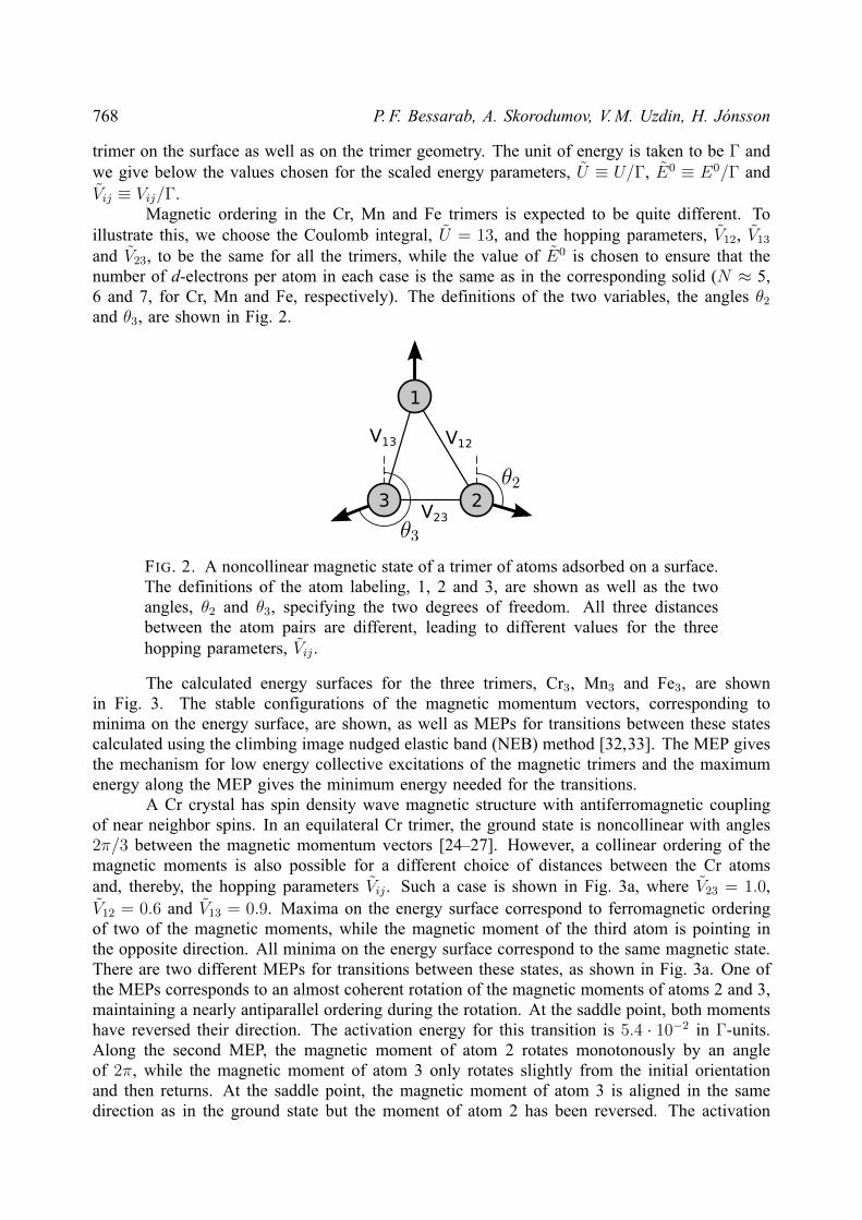
768 P. F. Bessarab, A. Skorodumov, V. M. Uzdin, H. Jonsson
trimer on the surface as well as on the trimer geometry. The unit of energy is taken to be Γ andwe give below the values chosen for the scaled energy parameters, U ≡ U/Γ, E0 ≡ E0/Γ andVij ≡ Vij/Γ.
Magnetic ordering in the Cr, Mn and Fe trimers is expected to be quite different. Toillustrate this, we choose the Coulomb integral, U = 13, and the hopping parameters, V12, V13and V23, to be the same for all the trimers, while the value of E0 is chosen to ensure that thenumber of d-electrons per atom in each case is the same as in the corresponding solid (N ≈ 5,6 and 7, for Cr, Mn and Fe, respectively). The definitions of the two variables, the angles θ2and θ3, are shown in Fig. 2.
FIG. 2. A noncollinear magnetic state of a trimer of atoms adsorbed on a surface.The definitions of the atom labeling, 1, 2 and 3, are shown as well as the twoangles, θ2 and θ3, specifying the two degrees of freedom. All three distancesbetween the atom pairs are different, leading to different values for the threehopping parameters, Vij .
The calculated energy surfaces for the three trimers, Cr3, Mn3 and Fe3, are shownin Fig. 3. The stable configurations of the magnetic momentum vectors, corresponding tominima on the energy surface, are shown, as well as MEPs for transitions between these statescalculated using the climbing image nudged elastic band (NEB) method [32,33]. The MEP givesthe mechanism for low energy collective excitations of the magnetic trimers and the maximumenergy along the MEP gives the minimum energy needed for the transitions.
A Cr crystal has spin density wave magnetic structure with antiferromagnetic couplingof near neighbor spins. In an equilateral Cr trimer, the ground state is noncollinear with angles2π/3 between the magnetic momentum vectors [24–27]. However, a collinear ordering of themagnetic moments is also possible for a different choice of distances between the Cr atomsand, thereby, the hopping parameters Vij . Such a case is shown in Fig. 3a, where V23 = 1.0,V12 = 0.6 and V13 = 0.9. Maxima on the energy surface correspond to ferromagnetic orderingof two of the magnetic moments, while the magnetic moment of the third atom is pointing inthe opposite direction. All minima on the energy surface correspond to the same magnetic state.There are two different MEPs for transitions between these states, as shown in Fig. 3a. One ofthe MEPs corresponds to an almost coherent rotation of the magnetic moments of atoms 2 and 3,maintaining a nearly antiparallel ordering during the rotation. At the saddle point, both momentshave reversed their direction. The activation energy for this transition is 5.4 · 10−2 in Γ-units.Along the second MEP, the magnetic moment of atom 2 rotates monotonously by an angleof 2π, while the magnetic moment of atom 3 only rotates slightly from the initial orientationand then returns. At the saddle point, the magnetic moment of atom 3 is aligned in the samedirection as in the ground state but the moment of atom 2 has been reversed. The activation
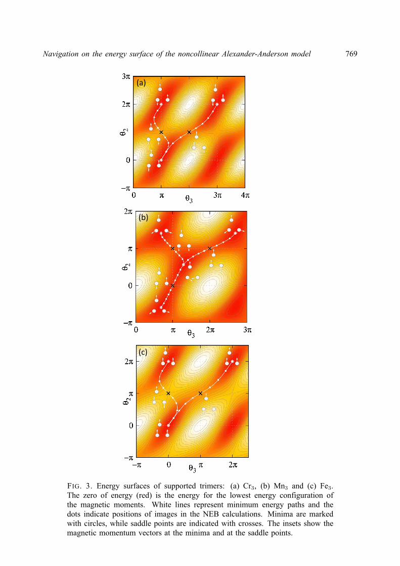
Navigation on the energy surface of the noncollinear Alexander-Anderson model 769
(a)
(b)
(c)
FIG. 3. Energy surfaces of supported trimers: (a) Cr3, (b) Mn3 and (c) Fe3.The zero of energy (red) is the energy for the lowest energy configuration ofthe magnetic moments. White lines represent minimum energy paths and thedots indicate positions of images in the NEB calculations. Minima are markedwith circles, while saddle points are indicated with crosses. The insets show themagnetic momentum vectors at the minima and at the saddle points.
770 P. F. Bessarab, A. Skorodumov, V. M. Uzdin, H. Jonsson
energy is larger for this second mechanism, 7.8 · 10−2 Γ, because of strong antiferromagneticcoupling between atoms 2 and 3. Note that all minima and saddle points on the energy surfacecorrespond to collinear ordering of the magnetic moments.
For the Mn trimer, we obtain two distinct stable states, both corresponding to non-collinear magnetic ordering, as shown in Fig 3b. Mn atoms often form noncollinear struc-tures [24, 26, 28]. The two stable states have the same energy, but the MEPs between them arequite different and give different activation energies. The saddle points correspond to collinearmagnetic ordering. The activation energy is 1.9 · 10−2 Γ for the saddle point at θ2 = π, θ3 = π,1.7 · 10−2 Γ for the saddle point at θ2 = π, θ3 = 2π and 0.7 · 10−2 Γ for the saddle points atθ2 = 0, θ3 = π.
For the Fe trimer, all the minima on the energy surface correspond to the same ferro-magnetic state (see Fig. 3c). The saddle points between those states also correspond to collinearmagnetic ordering, but with one of the magnetic moments pointing in the opposite directionto the other two. The energy surface for the Fe trimer is similar to the one for the Cr trimer,but shifted by π along the θ3 axis. There are also two possible MEPs between the states. TheMEP with the lower activation energy, 2.7 · 10−2 Γ, corresponds to nearly coherent rotation ofthe second and the third magnetic moments. The other MEP corresponds to relatively smalldeviation of θ3 from zero. The barrier for this transition mechanism is higher, 4.5 · 10−2 Γ.
4.2. STM tip interacting with adsorbed dimer
The energy surface of a magnetic cluster can be modified by applying a local externalmagnetic field. Another way to deform the surface is by hybridization with an additional atomplaced close enough to the cluster. The latter effect was recently demonstrated experimentallyby using magnetic atoms at the tip of a scanning-tunneling microscope (STM) [34]. Themagnetic tip was used to modify the energy barrier between two magnetic states of a magneticnanostructure on a non-magnetic substrate.
As a simple model of this experiment, we consider the isosceles Cr trimer, where atom 1represents the STM tip and atoms 2 and 3 represent the dimer adsorbed on a non-magneticsubstrate. The hopping parameters between the tip atom and each one of the two dimer atomsare set to be the same, V12 = V13 ≡ V , and are varied to mimic changes in the distance betweenthe tip and the dimer, while the third hopping parameter is kept fixed with a value of V23 = 1.For each value of V , the energy of the system is minimized with respect to the angles θ2 andθ3 defining the orientation of the magnetic moments in the dimer. Due to the symmetry of thesystem, θ2 differs from θ3 by an angle of π at the minimum energy configuration. The valueobtained for one of the angles, θ2, is shown as a function of V in Fig. 4. For small V , themagnetic moments of the dimer point in the opposite direction and are perpendicular to themagnetic moment of the tip. However, when V becomes larger than V23, the magnetic momentsof the dimer tend to point in the same direction and opposite to the magnetic moment of thetip. The energy surface of the system for three different values of V is shown in the insets ofFig. 4.
5. Finite range approximation
In the self-consistency calculations, the computational effort of the tridiagonalization ofthe NCAA Hamiltonian which is needed to evaluate the matrix elements of the Green functionscales as P 3, where P is the number of magnetic atoms in the system. This operation has tobe performed for each magnetic atom, so the computational effort in each iteration of the self-consistency procedure scales as P 4. The number of iterations needed to reach self-consistency
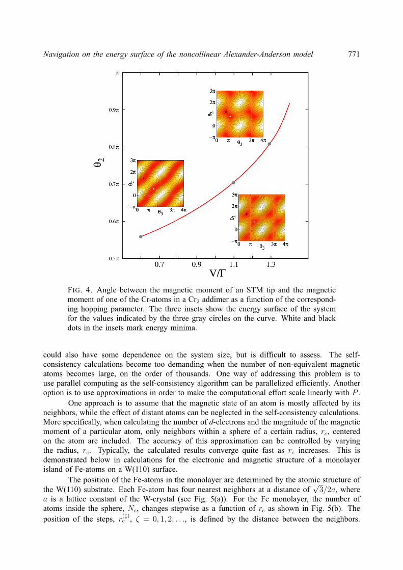
Navigation on the energy surface of the noncollinear Alexander-Anderson model 771
FIG. 4. Angle between the magnetic moment of an STM tip and the magneticmoment of one of the Cr-atoms in a Cr2 addimer as a function of the correspond-ing hopping parameter. The three insets show the energy surface of the systemfor the values indicated by the three gray circles on the curve. White and blackdots in the insets mark energy minima.
could also have some dependence on the system size, but is difficult to assess. The self-consistency calculations become too demanding when the number of non-equivalent magneticatoms becomes large, on the order of thousands. One way of addressing this problem is touse parallel computing as the self-consistency algorithm can be parallelized efficiently. Anotheroption is to use approximations in order to make the computational effort scale linearly with P .
One approach is to assume that the magnetic state of an atom is mostly affected by itsneighbors, while the effect of distant atoms can be neglected in the self-consistency calculations.More specifically, when calculating the number of d-electrons and the magnitude of the magneticmoment of a particular atom, only neighbors within a sphere of a certain radius, rc, centeredon the atom are included. The accuracy of this approximation can be controlled by varyingthe radius, rc. Typically, the calculated results converge quite fast as rc increases. This isdemonstrated below in calculations for the electronic and magnetic structure of a monolayerisland of Fe-atoms on a W(110) surface.
The position of the Fe-atoms in the monolayer are determined by the atomic structure ofthe W(110) substrate. Each Fe-atom has four nearest neighbors at a distance of
√3/2a, where
a is a lattice constant of the W-crystal (see Fig. 5(a)). For the Fe monolayer, the number ofatoms inside the sphere, Nc, changes stepwise as a function of rc as shown in Fig. 5(b). Theposition of the steps, r(ζ)c , ζ = 0, 1, 2, . . ., is defined by the distance between the neighbors.
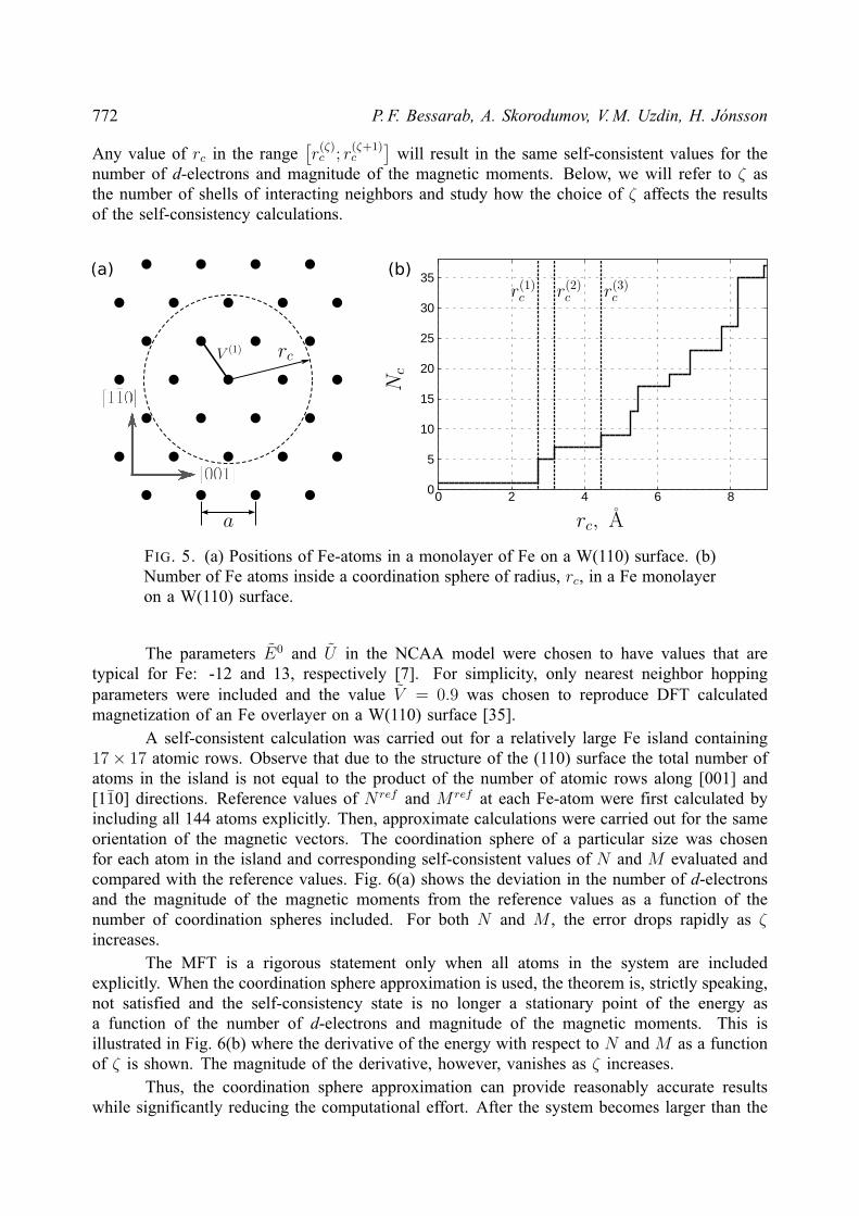
772 P. F. Bessarab, A. Skorodumov, V. M. Uzdin, H. Jonsson
Any value of rc in the range[r(ζ)c ; r
(ζ+1)c
]will result in the same self-consistent values for the
number of d-electrons and magnitude of the magnetic moments. Below, we will refer to ζ asthe number of shells of interacting neighbors and study how the choice of ζ affects the resultsof the self-consistency calculations.
FIG. 5. (a) Positions of Fe-atoms in a monolayer of Fe on a W(110) surface. (b)Number of Fe atoms inside a coordination sphere of radius, rc, in a Fe monolayeron a W(110) surface.
The parameters E0 and U in the NCAA model were chosen to have values that aretypical for Fe: -12 and 13, respectively [7]. For simplicity, only nearest neighbor hoppingparameters were included and the value V = 0.9 was chosen to reproduce DFT calculatedmagnetization of an Fe overlayer on a W(110) surface [35].
A self-consistent calculation was carried out for a relatively large Fe island containing17× 17 atomic rows. Observe that due to the structure of the (110) surface the total number ofatoms in the island is not equal to the product of the number of atomic rows along [001] and[110] directions. Reference values of N ref and M ref at each Fe-atom were first calculated byincluding all 144 atoms explicitly. Then, approximate calculations were carried out for the sameorientation of the magnetic vectors. The coordination sphere of a particular size was chosenfor each atom in the island and corresponding self-consistent values of N and M evaluated andcompared with the reference values. Fig. 6(a) shows the deviation in the number of d-electronsand the magnitude of the magnetic moments from the reference values as a function of thenumber of coordination spheres included. For both N and M , the error drops rapidly as ζincreases.
The MFT is a rigorous statement only when all atoms in the system are includedexplicitly. When the coordination sphere approximation is used, the theorem is, strictly speaking,not satisfied and the self-consistency state is no longer a stationary point of the energy asa function of the number of d-electrons and magnitude of the magnetic moments. This isillustrated in Fig. 6(b) where the derivative of the energy with respect to N and M as a functionof ζ is shown. The magnitude of the derivative, however, vanishes as ζ increases.
Thus, the coordination sphere approximation can provide reasonably accurate resultswhile significantly reducing the computational effort. After the system becomes larger than the
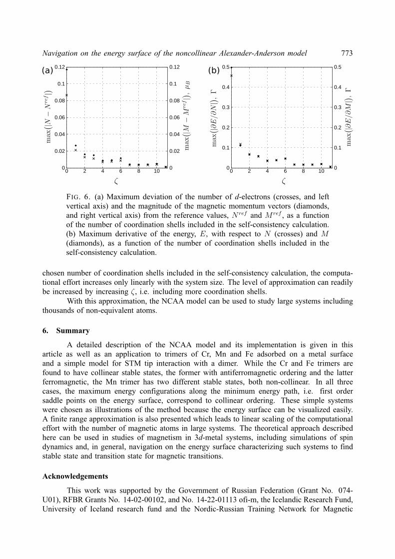
Navigation on the energy surface of the noncollinear Alexander-Anderson model 773
FIG. 6. (a) Maximum deviation of the number of d-electrons (crosses, and leftvertical axis) and the magnitude of the magnetic momentum vectors (diamonds,and right vertical axis) from the reference values, N ref and M ref , as a functionof the number of coordination shells included in the self-consistency calculation.(b) Maximum derivative of the energy, E, with respect to N (crosses) and M(diamonds), as a function of the number of coordination shells included in theself-consistency calculation.
chosen number of coordination shells included in the self-consistency calculation, the computa-tional effort increases only linearly with the system size. The level of approximation can readilybe increased by increasing ζ , i.e. including more coordination shells.
With this approximation, the NCAA model can be used to study large systems includingthousands of non-equivalent atoms.
6. Summary
A detailed description of the NCAA model and its implementation is given in thisarticle as well as an application to trimers of Cr, Mn and Fe adsorbed on a metal surfaceand a simple model for STM tip interaction with a dimer. While the Cr and Fe trimers arefound to have collinear stable states, the former with antiferromagnetic ordering and the latterferromagnetic, the Mn trimer has two different stable states, both non-collinear. In all threecases, the maximum energy configurations along the minimum energy path, i.e. first ordersaddle points on the energy surface, correspond to collinear ordering. These simple systemswere chosen as illustrations of the method because the energy surface can be visualized easily.A finite range approximation is also presented which leads to linear scaling of the computationaleffort with the number of magnetic atoms in large systems. The theoretical approach describedhere can be used in studies of magnetism in 3d-metal systems, including simulations of spindynamics and, in general, navigation on the energy surface characterizing such systems to findstable state and transition state for magnetic transitions.
Acknowledgements
This work was supported by the Government of Russian Federation (Grant No. 074-U01), RFBR Grants No. 14-02-00102, and No. 14-22-01113 ofi-m, the Icelandic Research Fund,University of Iceland research fund and the Nordic-Russian Training Network for Magnetic

774 P. F. Bessarab, A. Skorodumov, V. M. Uzdin, H. Jonsson
Nanotechnology (NCM-RU10121). PB greatly acknowledges support from Goran GustafssonFoundation.
APPENDIX
A. Recursion method and continued-fraction expansion of the Green function
An efficient algorithm for calculating the matrix elements of the Green function G (inthis Appendix, a dependence of G on ε is implied) using the recursion method involves findinga new orthonormal basis in which the Hamiltonian has a tridiagonal form, while the matrixelement to be evaluated, Gαβ
ij , remains unchanged.We begin by discussing how diagonal matrix elements, Gµµ = 〈xµ|G |xµ〉, can be
evaluated. Here,|x1〉 , . . . , |x2P 〉
is an initial basis set and indices µ, ν enumerate both
atomic site and spin projection. The first vector of the new basis is chosen so that |y1〉 = |xµ〉.Then, the diagonal matrix element of the Green function is given by:
Gµµ = 〈y1|G |y1〉 = G11, (41)
where tilde indicates a quantity in the new basis. Other vectors of the new basis|y1〉 , . . . , |y2P 〉
are found given that the Hamiltonian has a tridiagonal form:
Hµν =
a1 b1 0 0 . . . 0 0 0
b1 a2 b2 0 . . . 0 0 0
0 b2 a3 b3 . . . 0 0 0...
......
.... . .
......
...0 0 0 0 . . . a2P−2 b2P−2 0
0 0 0 0 . . . b2P−2 a2P−1 b2P−10 0 0 0 . . . 0 b2P−1 a2P
. (42)
Not only basis vectors |yµ〉 are found within the recursion scheme, but also elementsa1, a2, . . . , a2P and b1, b2, . . . , b2P−1 are successively calculated. From the equation:
H |y1〉 = a1 |y1〉+ b1 |y2〉 , (43)
the second basis vector |y2〉 as well as a1 and b1 can be found as follows:
a1 = 〈y1|H |y1〉 , (44)
b1 = ‖H |y1〉 − a1 |y1〉‖ , (45)
|y2〉 =H |y1〉 − a1 |y1〉
b1. (46)
Then, the Hamiltonian acts upon the second basis vector and the next portion of elementsof the tridiagonal matrix is found. This operation is reapplied until all elements of H in thenew basis have been calculated. For example, on the k-th step (k < 2P ), when a1, . . . , ak−1,b1, . . . , bk−1 and |y1〉 , . . . , |yk〉 are known, we have:
ak = 〈yk|H |yk〉 , (47)
bk = ‖H |yk〉 − bk−1 |yk−1〉 − ak |yk〉‖ , (48)
|yk+1〉 =H |yk〉 − bk−1 |yk−1〉 − ak |yk〉
bk. (49)
Navigation on the energy surface of the noncollinear Alexander-Anderson model 775
G11 is found in the following way. Let us introduce a notation:
λk = 〈y1|G |yk〉 . (50)
The following set of equations is then valid for λk, which follows from the definition of theGreen function, (ε−H)G = I:
(ε− a1)λ1 − b1λ2 = 1,
(ε− ak)λk − bk−1λk−1 − bkλk+1 = 0, k 6= 1, k 6= 2P,
(ε− a2P )λ2P − b2P−1λ2P−1 = 0.
After straightforward algebra, we obtain the representation of G11 in the continued-fractionform:
Gµµ = G11 = λ1 =1
ε− a1 −b21
ε− a2 −· · ·
· · · −b22P−1ε− a2P
(51)
The nondiagonal elements of the Green function can also be expanded in terms ofcontinued fractions. Namely, if Gµν , µ 6= ν, is to be found, one has to perform tridiagonalizationfour times, where the starting vectors are:
|ya1〉 =1√2
(|xµ〉+ |xν〉) ,∣∣yb1⟩ =1√2
(|xµ〉 − |xν〉) ,
|yc1〉 =1√2
(|xµ〉+ i |xν〉) ,∣∣yd1⟩ =1√2
(|xµ〉 − i |xν〉) .
In each basis, matrix element Gζ11 =
⟨yζ1
∣∣∣G ∣∣∣yζ1⟩, ζ = a, b, c, d, is expanded in terms of contin-
ued fractions as described above. Continued-fraction representation of the real and imaginarypart of the nondiagonal element, Gµν , is thus given by:
ReGµν =1
2
(Ga
11 − Gb11
), (52)
ImGµν =1
2
(Gd
11 − Gc11
). (53)
B. Partial-fraction expansion of the Green function
We proceed with the continued-fraction representation of the matrix element of the Greenfunction, Eqn. (51). Let us consider the last level of the continued fraction:
f (1)(ε) = ε− a2P−1 −b22P−1ε− a2P
. (54)
776 P. F. Bessarab, A. Skorodumov, V. M. Uzdin, H. Jonsson
If b2P−1 6= 0, then the equation f (1)(ε) = 0 has two real roots, q(2)1 and q(2)2 , q(2)1 < q(2)2 , which
can be found either analytically or numerically. Then:
f (1)(ε) =
(ε− q(2)1
)(ε− q(2)2
)ε− q(1)1
,
where q(1)1 ≡ a2P . As a result, the next level of the continued fraction acquires the form:
f (2)(ε) = ε− a2P−2 −b22P−2
(ε− q(1)1
)(ε− q(2)1
)(ε− q(2)2
) .The ratio of polynomials here can be transformed into a sum of two partial fractions:
b22P−2
(ε− q(1)1
)(ε− q(2)1
)(ε− q(2)2
) =p(2)1
ε− q(2)1
+p(2)2
ε− q(2)2
,
where
p(2)1 = b22P−2
q(2)1 − q
(1)1
q(2)1 − q
(2)2
, p(2)2 = b22P−2
q(2)2 − q
(1)1
q(2)2 − q
(2)1
.
Thus, the function f 2(ε) is represented in the form analogous to Eqn. (54):
f (2)(ε) = ε− a2P−2 −p(2)1
ε− q(2)1
− p(2)2
ε− q(2)2
, (55)
and the number of levels in the continued fraction is reduced by one.The same technique is sequentially applied in order to transform the continued fraction
into a sum of partial fractions. For example, at the k-th step we have:
f (k)(ε) = ε− a2P−k −k∑j=1
p(k)j
ε− q(k)j
. (56)
Zeros of the function f (k)(ε) are well separated (see Fig. 7) and can be found numericallywithout problems.
The function f (k+1)(ε) is then represented as follows:
f (k+1)(ε) = ε− a2P−k−1 −k+1∑j=1
p(k+1)j
ε− q(k+1)j
.
Here q(k+1)1 , . . . , q
(k+1)k+1 are the roots of f (k)(ε) = 0 and p(k+1)
j are given by:
p(k+1)j = b22P−k−1
k∏i=1
(q(k+1)j − q(k)i
)k+1∏i=1i6=j
(q(k+1)j − q(k+1)
i
) .As a result, any continued fraction of the form (51) and thus an arbitrary element of the Greenfunction can be expanded in a sum of partial fractions (see Eqn. (29)).
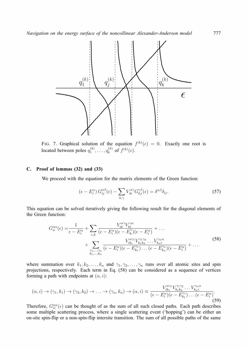
Navigation on the energy surface of the noncollinear Alexander-Anderson model 777
FIG. 7. Graphical solution of the equation f (k)(ε) = 0. Exactly one root islocated between poles q(k)1 , . . . , q
(k)k of f (k)(ε).
C. Proof of lemmas (32) and (33)
We proceed with the equation for the matrix elements of the Green function:
(ε− Eαi )Gαβ
ij (ε)−∑k,γ
V αγik G
γβkj (ε) = δαβδij. (57)
This equation can be solved iteratively giving the following result for the diagonal elements ofthe Green function:
Gααii (ε) =
1
ε− Eαi
+∑γ,k
V αγik V
γαki
(ε− Eαi )(ε− Eγ
k )(ε− Eαi )
+ . . .
+∑
γ1,...,γnk1,...,kn
V αγ1ik1
V γ1γ2k1k2
. . . V γnαkni
(ε− Eαi )(ε− Eγ1
k1) . . . (ε− Eγn
kn)(ε− Eα
i )+ . . .
(58)
where summation over k1, k2, . . . , kn and γ1, γ2, . . . , γn runs over all atomic sites and spinprojections, respectively. Each term in Eq. (58) can be considered as a sequence of verticesforming a path with endpoints at (α, i):
(α, i)→ (γ1, k1)→ (γ2, k2)→ . . .→ (γn, kn)→ (α, i) ≡V αγ1ik1
V γ1γ2k1k2
. . . V γnαkni
(ε− Eαi )(ε− Eγ1
k1) . . . (ε− Eα
i ).
(59)Therefore, Gαα
ii (ε) can be thought of as the sum of all such closed paths. Each path describessome multiple scattering process, where a single scattering event (‘hopping’) can be either anon-site spin-flip or a non-spin-flip intersite transition. The sum of all possible paths of the same
778 P. F. Bessarab, A. Skorodumov, V. M. Uzdin, H. Jonsson
length and endpoints fixed at (α, i) can be represented as:∑γ1,...,γnk1,...,kn
V αγ1ik1
V γ1γ2k1k2
. . . V γnαkni
(ε− Eαi )(ε− Eγ1
k1) . . . (ε− Eγn
kn)(ε− Eα
i )=[G0(ε)V G0(ε)V . . . V︸ ︷︷ ︸
n+1 V -factors
G0(ε)]ααii≡ Sααii (ε;n).
(60)Here, V is a hopping matrix (see Eq. (19)) which contains information about all scattering eventsin the system and G0(ε) is the Green function for the non-interacting magnetic impurities. G0(ε)is diagonal and its matrix elements are given by:
[G0(ε)]ααii =
1
(ε− Eαi ). (61)
In order to prove lemmas (32)-(33), it is sufficient to derive corresponding identities forthe sum of the paths, S(ε;n), for an arbitrary path length, n. The derivative of TrS(ε;n) withrespect to Ni is given by:
∂
∂Ni
TrS(ε;n) =∂
∂Ni
Tr [G0(ε)V G0(ε)V . . . V G0(ε)] = Tr
[∂G0(ε)
∂Ni
V G0(ε)V . . . V G0(ε)
]+ Tr
[G0(ε)V
∂G0(ε)
∂Ni
V . . . V G0(ε)
]+ . . .+ Tr
[G0(ε)V G0(ε)V . . . V
∂G0(ε)
∂Ni
].
(62)
Only two matrix elements of∂G0(ε)
∂Ni
are non-zero (see Eq. (61)). According to Eqs. (61) and
(18), they can be expressed in terms of derivatives with respect to ε :
∂G0(ε)
∂Ni
= −Ui2
∂G0(ε)
∂εΣ0i , (63)
where Σ0i is 2P × 2P matrix defined so that only the elements (++, ii) and (−−, ii) are equal
to unity, while the others are zero. Therefore, Eq. (62) takes the form:
∂
∂Ni
TrS(ε;n) = −Ui2
Tr
[∂G0(ε)
∂εΣ0iV G0(ε)V . . . V G0(ε)
]+ Tr
[G0(ε)V
∂G0(ε)
∂εΣ0iV . . . V G0(ε)
]+ . . .+ Tr
[G0(ε)V G0(ε)V . . . V
∂G0(ε)
∂εΣ0i
].
(64)
The factor∂G0(ε)
∂εΣ0i found in every term in the curly brackets can be transformed into:
∂G0(ε)
∂εΣ0i = −G0(ε)Σ
0iG0(ε), (65)
where use has been made of the identity
∂G0(ε)
∂ε= −G2
0(ε), (66)
Navigation on the energy surface of the noncollinear Alexander-Anderson model 779
as well as commutativity of G0(ε) and Σ0i . Using Eqs. (65) and (66) and invariance of a trace
under cyclic permutations, each term in Eq. (64) is transformed to obtain the following:
∂
∂Ni
TrS(ε;n) = −Ui2
Tr
[Σ0i
∂G0(ε)
∂εV G0(ε)V . . . V G0(ε)
]+ Tr
[Σ0iG0(ε)V
∂G0(ε)
∂εV . . . V G0(ε)
]+ . . .+ Tr
[Σ0iG0(ε)V G0(ε)V . . . V
∂G0(ε)
∂ε
]= −Ui
2
∂
∂εTr[Σ0iG0(ε)V G0(ε)V . . . V G0(ε)
]=
= −Ui2
∂
∂εTr[Σ0iS(ε;n)
]= −Ui
2
∂
∂ε
(S++ii (ε;n) + S−−ii (ε;n)
),
(67)
which proves Lemma (32).Lemma (33) is proved in a similar way. However, when computing the derivative of
TrS(ε;n) with respect to Mi, one needs to observe that both G0(ε) and V depend on Mi. Morespecifically:
∂G0(ε)
∂Mi
=Ui2
cos θi∂G0(ε)
∂εΣzi , (68)
∂V
∂Mi
= −Ui2
sin θi (cosφiΣxi + sinφiΣ
yi ) . (69)
The only nonzero matrix elements of Σxi , Σy
i and Σzi are defined as follows:
(Σxi )
+−ii = 1 (Σx
i )−+ii = 1, (70)
(Σyi )
+−ii = −i (Σy
i )−+ii = i, (71)
(Σzi )
++ii = 1 (Σz
i )−−ii = −1. (72)
Note that if only one magnetic impurity is present in the system, Σxi , Σy
i and Σzi coincide with
ordinary 2× 2 Pauli matrices. This gives the following:
∂
∂Mi
TrS(ε;n) =Ui2
cos θi∂
∂εTr [Σz
iG0(ε)V G0(ε)V . . . V G0(ε)] +
Ui2
sin θi∂
∂ε
(cosφi Tr [Σx
iG0(ε)V G0(ε)V . . . V G0(ε)] + sinφi Tr [ΣyiG0(ε)V G0(ε)V . . . V G0(ε)]
)=Ui2
∂
∂ε
cos θi Tr [Σz
iS(ε;n)] + sin θi
(cosφi Tr [Σx
i S(ε;n− 1)] + sinφi Tr [ΣyiS(ε;n− 1)]
)=Ui2
∂
∂ε
[(S++ii (ε;n)− S−−ii (ε;n)
)cos θi +
(S+−ii (ε;n− 1)eφi + S−+ii (ε;n− 1)e−φi
)sin θi
],
(73)
which proves lemma (33).For large (or infinite) systems, the calculation of Green functions is often performed
approximately, using a finite range approximation (see Sec. 5) or by truncating the recursionmethod (see appendix A) at a certain step. In this case, the scattering matrix Vi may be differentfor different sites i and Lemmas (32)-(33) and, therefore, the MFT, are strictly not valid. Thiswas demonstrated in Sec. 5 where direct calculations of the derivatives of energy with respectto Ni and Mi for the self-consistent values N∗i and M∗
i were found not to equal zero becauseof the finite range approximation. However, if any subsystem of atoms is chosen and the same
780 P. F. Bessarab, A. Skorodumov, V. M. Uzdin, H. Jonsson
set of hopping contributions are included for all the atoms of this subsystem, then the scatteringmatrix will be the same for all atoms in the system and the proof of Lemmas (32)-(33) willhold just as in the case when all atoms and hopping contributions are included. In particular,one can choose as a subsystem the atoms included in one closed loop in Eqn.(59) and thecorresponding hopping contributions to form the scattering matrix V . Then, the MFT will bevalid for this subsystem. Formally, it is a consequence of the fact that all closed paths inEqn.(59) which make a contribution to the matrix element of the Green function Gii, make thesame contribution to any Gjj if the path in Eqn.(59) goes through site j. If, however, we try toimprove the calculation by taking into account additional atoms and hopping contributions thatare different for different atoms, as in the case of the finite range approximation described inSec. 5, then the MFT is violated.
References
[1] R. Wiesendanger. Spin mapping at the nanoscale and atomic scale. Rev. Mod. Phys., 81, 1495 (2009).[2] S. Heinze, K. von Bergmann, et al. Spontaneous atomic-scale magnetic skyrmion lattice in two dimensions.
Nature Phys. 7, 713 (2011).[3] M. Bode, O. Pietzsch, et al. Experimental Evidence for Intra-Atomic Noncollinear Magnetism at Thin Film
Probe Tips. Phys. Rev. Lett. 86, 2142 (2001).[4] P.F. Bessarab, V.M. Uzdin, H. Jonsson. Harmonic transition state theory of thermal spin transitions. Phys.
Rev. B 85, 184409 (2012).[5] H.B. Braun. Topological effects in nanomagnetism: from superparamagnetism to chiral quantum solitons.
Advances in Physics 61, 1 (2012).[6] P.F. Bessarab, V.M. Uzdin, H. Jonsson. Size and shape dependence of thermal spin transitions in nanoislands.
Phys. Rev. Lett. 110, 020604 (2013).[7] P.F. Bessarab, V.M. Uzdin, H. Jonsson. Potential Energy Surfaces and Rates of Spin Transitions. Z. Phys.
Chem. 227, 1543 (2013).[8] T. Oda, A. Pasquarello, R. Car. Fully Unconstrained Approach to Noncollinear Magnetism: Application to
Small Fe Clusters. Phys. Rev. Lett. 80, 3622 (1998).[9] O. Ivanov, V.P. Antropov. Molecular magnetism: Noncollinear ordering and spin dynamics. J. Appl. Phys. 85,
4821 (1999).[10] L. Nordstrom, D.J. Singh. Noncollinear intra-atomic magnetism. Phys. Rev. Lett. 76, 4420 (1996).[11] V.P. Antropov, M.I. Katsnelson, et al. Spin dynamics in magnets: equation of motion and finite temperature
effects. Phys. Rev. B 54, 1019-1035 (1996).[12] L.M. Small, V. Heine. A couple method for calculating interatomic interactions in itinerant electron magnetic
systems. J. Phys. F 14, 3041 (1986).[13] G. Bihlmayer, ‘Density-functional theory of magnetism’, in ‘Handbook of magnetism and advanced magnetic
materials’, ed. H. Kronmuller, S. Parkin. Vol. 1, page 3.[14] L.M. Sandratskii. Noncollinear magnetism in itinerant-electron systems: Theory and applications. Advances
in Physics 47, 91 (1998).[15] G.M. Stocks , B. Ujfalussy, et al. Towards a constrained local moment model for first principles spin dynamics.
Philos. Mag. B 78, 665 (1998).[16] S. Lounis, P.H. Dederichs. Mapping the magnetic exchange interactions from first principles: Anisotropy
anomaly and application to Fe, Ni, and Co. Phys. Rev. B 82, 180404(R) (2010).[17] P.W. Anderson. Localized Magnetic States in Metals. Phys. Rev. 124, 41 (1961).[18] S. Alexander, P.W. Anderson. Interaction between localized states in metals. Phys. Rev. 133, A1594 (1964).[19] R. Haydock, V. Heine, M.J. Kelly. Electronic structure based on the local atomic environment for tight-binding
bands. J. Phys. C: Solid State Phys. 5, 2845 (1972).[20] R. Haydock, V. Heine, M.J. Kelly. Electronic structure based on the local atomic environment for tight-binding
bands: II. J. Phys. C: Solid State Phys. 8, 2591 (1975).[21] V.M. Uzdin, N.S. Yartseva. Periodic Anderson model for the description of noncollinear magnetic structure
in low-dimensional 3d-systems. Comput. Mater. Sci. 10, 211 (1998).[22] S.V. Uzdin. On the calculation of the magnetic structure of surfaces, near surface layers, and interfaces of 3d
metals. Physics of the Solid State 51, 1260 (2009).
Navigation on the energy surface of the noncollinear Alexander-Anderson model 781
[23] P.F. Bessarab, V.M. Uzdin, H. Jonsson. Calculations of magnetic states and minimum energy paths of transi-tions using a noncollinear extension of the Alexander-Anderson model and a magnetic force theorem. Phys.Rev. B 89, 214424 (2014).
[24] S. Uzdin, V. Uzdin, C. Demangeat. Magnetic trimer on non-magnetic substrate: from frustration towardsnon-collinearity. Europhys. Lett. 47, 556 (1999).
[25] S. Uzdin, V. Uzdin, C. Demangeat. Non-collinear structure of Cr trimer on the surface of non-magneticmetals. Comput. Mater. Sci. 17, 441 (2000).
[26] S. Uzdin, V. Uzdin, C. Demangeat. Non-collinear magnetism of Cr, Mn and Fe trimers supported on thenon-magnetic metal surface. Surf. Sci. 482, 965 (2001).
[27] H.J. Gotsis, N. Kioussis, D.A. Papaconstantopoulos. Evolution of magnetism of Cr nanoclusters on Au(111):First-principles electronic structure calculations. Phys. Rev. B 73, 014436 (2006).
[28] A. Bergman, L. Nordstrom, et al. Magnetic interactions of Mn clusters supported on Cu. Phys. Rev. B 73,174434 (2006).
[29] K. Hirai. Electronic Structure of Helical Spin Density Wave State in fcc Iron. J. Phys. Soc. of Jpn. 61, 2491(1992).
[30] S. Lounis, P. Mavropoulos, P.H. Dederichs, S. Blugel. Noncollinear Korringa-Kohn-Rostoker Green functionmethod: Application to 3d nanostructures on Ni (001). Phys. Rev. B 72, 224437 (2005).
[31] R. Robles, L. Nordstrom. Noncollinear magnetism of Cr clusters on Fe surfaces. Phys. Rev. B 74, 094403(2006).
[32] H. Jonsson, G. Mills, K.W. Jacobsen. In Classical and Quantum Dynamics in Condensed Phase Simulations,edited by B.J. Berne, G. Ciccotti, D. F. Coker (World Scientific, Singapore, 1998), p. 385.
[33] G. Henkelman, H. Jonsson. ‘Improved Tangent Estimate in the NEB Method for Finding Minimum EnergyPaths and Saddle Points’. J. Chem. Phys. 113, 9978 (2000).
[34] R. Schmidt, A. Schwarz, R. Wiesendanger. Ground State of Magnetic Dimers on Metal Surfaces. Phys. Rev.B 86 174402 (2012).
[35] A.T. Costa, R.B. Muniz, et al. Magnetism of an Fe monolayer on W(110). Phys. Rev. B 78 054439 (2008).
NANOSYSTEMS: PHYSICS, CHEMISTRY, MATHEMATICS, 2014, 5 (6), P. 782–788
THE EFFECT OF THE CELL PHONERADIATION ON A FREELY SUSPENDED
LIQUID-CRYSTAL FILMS
A.A. Bogdanov1, S. P. Denisov2, A.A. Karetnikov3,A. P. Kovshik3, V. P. Romanov3, D. Brukkel 2
1The Federal State Budgetary Institute “The Nikiforov Russian Center of Emergencyand Radiation Medicine”, Saint Petersburg, Russia
2Center of Informatics “GAMMA-7”, Moscow, Russia3Saint Petersburg State University, Saint Petersburg, Russia
PACS 61.30.-v, 42.25.Lc, 42.70.Df, 41.85.Ct
The article presents the results of an experimental study of the effect of the radiofrequency radiation (RF)
of a cell phone on a freely suspended liquid-crystal film (FSLCF) as a system that simulates biological
structures. The selection of the FSLCF model is theoretically substantiated. A polarizing microscope with
a video camera was used to visualize the process under study. The reaction of the FSLCF was analyzed
using a specially developed software. The responses of the FSLCF were studied for exposure to the RF
radiation in the presence of protective device Gamma 7.N-RT and for the action of a static magnetic field
of strength 500 Oe. The RF radiation of a cell phone was found to change the orientation structure of the
FSLCF, which, after some time, returns to the nearly initial level despite the presence of external field.
The protective device Gamma 7.N-RT attenuates the reaction of the FSLCF. The response of the FSLCF
in a static magnetic field remains unchanged during the exposure to the field. These experimental results
are evidence that the structure of the freely suspended liquid-crystal film is a viable model for biological
structures, and is capable of adapting to the effect of the RF radiation emitted by a cell phone.
Keywords: biological structures, liquid-crystal film, electromagnetic fields, orientation structure.
Received: 31 October 2014
1. Introduction
The intense advancement of wireless technologies and the spread of mobile telecom-munication facilities in every-day life are among the primary reasons that people are per-sistently under the influence of low-energy RF electromagnetic fields. Despite the fact thatthere are numerous studies [1–4] on the matter, the issue of the biological effects of low-intensity electromagnetic fields on human and other organisms remains debatable [5–7].
The electromagnetic wave energy of a cell phone’s RF radiation is known to beinsufficient to break chemical bonds. The revealed biological effects are discussed primarily interms of the thermal exposure of electromagnetic radiation (EMR) [8]. However, a number ofnonthermal biological effects caused by low-energy electromagnetic radiation are described inthe literature [3,4]. These studies have questioned the hypothesis of the thermal nature of thebiological effects and the currently accepted safety levels of the EMR. These effects, caused bythe low-energy electromagnetic radiation comprise the increased permeability of the blood-brain barrier, changing the expression of heat shock genes, impaired calcium homeostasis,reduction of melatonin synthesis, etc. [4,9–11]. These biological effects can modify adaptive
The effect of the cell phone radiation... 783
processes in the organism. Therefore, studying the adaptive response patterns at differentlevels for the organism structure under exposure to low-energy EMR is an important andurgent task both in terms of understanding of the biological action mechanisms and assessingthe hazard this factor presents to human health.
In addition to the biological research, it is of interest to study the effect of the RFradiation on the systems that simulate real biological objects. The advantage for such studiesis that these make it possible to obtain quantitative data, permitting rigorous theoreticalanalysis.
Many biological structures are known to possess a number of properties which aretypical for liquid crystals [12]. These include chloroplasts, visual receptors, muscle, nerve, cellmembranes, etc. Therefore, a study of the influence of the RF radiation on the model crystalstructures may elucidate some of the mechanisms of biological reactions to this radiation.
Nematic liquid crystals are highly sensitive to the effects of external electric andmagnetic fields [13]. This makes liquid crystals the basis for displays as well as systems ofinformation transfer and storage. First of all, these are light modulators, displays, monitors,etc. In these devices, a thin layer of the liquid crystal is placed between the glass surfacesthat preset the specific direction of the optical axis of the liquid crystal (the direction of thepreferred orientation of the molecules). Under the action of an external electric field of asufficient strength that exceeds the threshold value, the direction of the optical axis alters,which affects the intensity of light passing through the liquid-crystal layer.
The energy density W required to change the orientation direction of the liquid crystalplaced between the glass surfaces is estimated by the relation [14]:
W ∼ K
d2,
where d is the layer thickness and K is the modulus of orientation elasticity of the orderof 10−6 dyn [13]. For the oriented layers with a thickness of 3 to 30 µm the energy den-sity required to change the direction of orientation of the liquid crystal is on the order ofW ∼ 0.1− 10 erg/cm3, which is much larger than that of cell phone RF radiation.
In all likelihood, the orientation of liquid-crystal structures in biological objects isfixed more weakly than on the solid surfaces of technical devices. Therefore, to cope withthe stated problem, we used a freely suspended film of a nematic liquid crystal as a liquid-crystal system, which, in our opinion, is most similar to biological structures and could beresponsive to the RF radiation of cell phones. In such a film, the process of changing thedirection of the preferred orientation of the liquid crystal molecules is nonthreshold [15]. Theenergy density required for the reorientation of the liquid crystal in a freely suspended film orfor the disordered-to-ordered state formation by an external field is estimated asK/L2, whereL is the dimension within which the external field can be considered homogeneous. Thisvalue is on the order of several fractions of millimeter to several millimeters. For these fields,the energy density required for the reorientation is on the order of W ∼ K/L2 ∼ 10−5 − 10−3
erg/cm2, that is, by several orders of magnitude lower than that required for the reorientationof a liquid crystal placed between the solid surfaces. It is the nonthreshold nature of thereorientation in a freely suspended liquid-crystal film that can provide its extremely highsensitivity to the external effects.
Cell phone radiation density near the phone is known to be on the order of 2-20 mW/cm3. The dielectric constant of liquid crystal at frequencies of several GHz isapproximately 3. This means that the energy density acting on the liquid crystal insidethe film amounts to 10−6 − 10−5 erg/cm3. By an order of magnitude, this energy densityis comparable with the energy of the orientational ordering. The aim of this study is to
784 A.A. Bogdanov, S. P. Denisov, et al.
investigate the effect of cell phone RF radiation on freely suspended films of a nematic liquidcrystal.
2. Materials and Methods
To study the effects of the RF radiation on the freely suspended liquid-crystal film,we used an experimental setup that enabled us to visually observe and record the structuralchanges in the film. The setup comprised a polarizing microscope POLAM L-213M equippedwith a video camera DCM-130 with a 1.3 megapixel photodetector array, and a PC with adisplay. The liquid-crystal film was composed of a binary mixture of alkylcyanobiphenylswas suspended on the wall of a circular aperture 2 mm in diameter in a plastic plate 0.5-mm thick and placed on the stage of the polarizing microscope. A cell phone Nokia-3110,operating in the signal transmission mode, was placed at a distance of 2 cm from the film.The linearly polarized light flux was directed normal to the film surface and arrived at thevideo camera through the objective of the microscope. The digitized 40-fold zoomed imagewas transmitted to the PC for viewing and recording. The light source was an incandescentlamp energized from a rectifier or a battery-powered LED.
The response of the liquid-crystal film to the influence of the RF radiation was as-sessed visually by changes in the distribution of light intensity and its color spectrum.
To compare the responses to different EM field effects, the freely suspended liquid-crystal film was also subjected to the action of a static magnetic field of strength 500 Oe.
Quantification of the freely suspended liquid-crystal film’s reaction was performedusing specially developed software. The observation field was selected as a section of thefilm free of the boundary effects occurring at the contact of the film with the aperturewall [16]. The image analysis technique is based on the count of the number of pixels withdifferent color codes in the RGB24 system. At the first stage, the number of pixels of eachcolor code in each frame was calculated and a histogram was constructed. At the secondstage, the number of non-recurrent color codes was determined from the histogram (thenumber of columns that contain non-zero values).
At the third stage, the ratio of the absolute number of the color codes per frameK andthe minimum number of the color codes during the observation period M was calculated.The time dependences of the expression (K/M) − 1 = N were plotted as graphs of thedynamic series.
3. The results of measurements
In the absence of a cell phone electromagnetic field (Fig. 1a), the freely suspendedliquid-crystal film has, at equilibrium, an anisotropic structure with a nonuniform spatialdistribution of the predominant direction of the long axes of the molecules (the local opticalaxis). This structure is formed under the action of the orienting forces of the molecules of thesurface layer, the cylindrical wall of the aperture at which the film is attached and, possibly,the electromagnetic fields acting in this spatial region. The light flux passing through thesystem has a nonuniform distribution of the intensity and spectral composition in the fieldof observation due to the inhomogeneous distribution of the local optical axis of the film.
During the first minute of exposure to the cell phone’s electromagnetic field thebrightness and color of the film alter (interference fringes appear), which may be associatedwith a local change in the spatial distribution of the optical axis in the film. Having reacheda maximum difference from the initial pattern (Fig. 1b), the image of the film changes again(interference fringes appear) and becomes similar to the original pattern (Fig. 1c). It shouldbe noted that, throughout this time, the film was exposed to the RF radiation of the cell
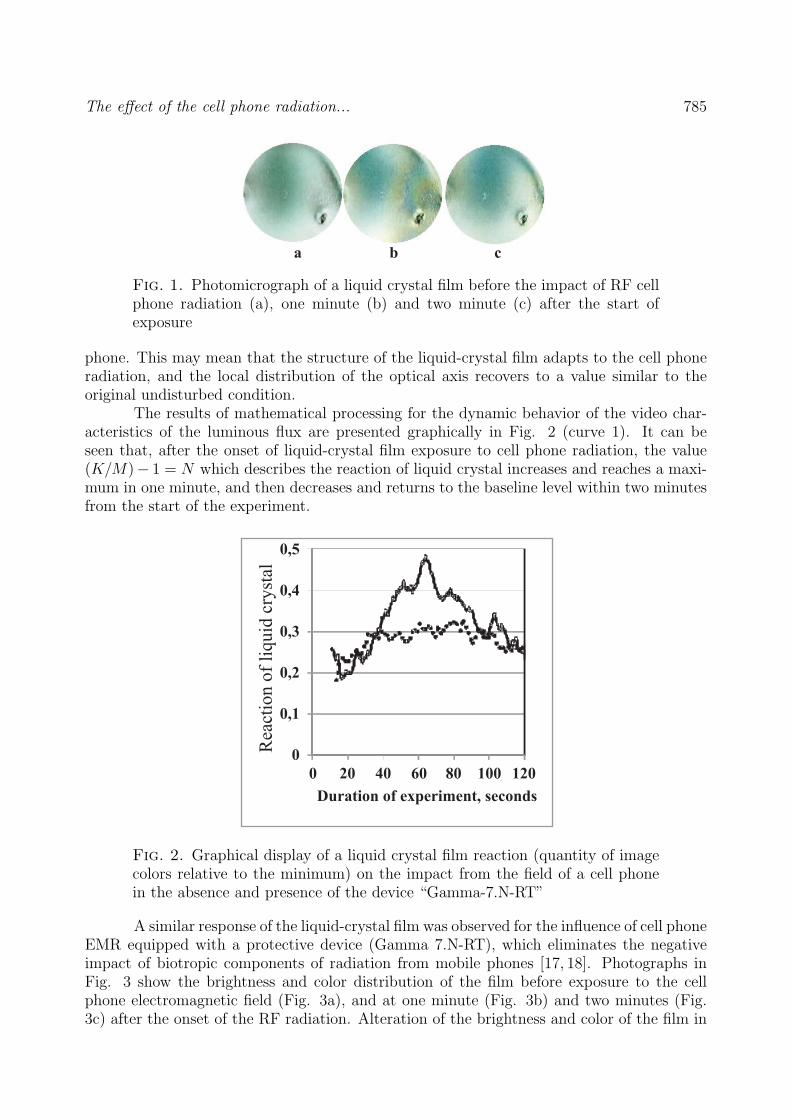
The effect of the cell phone radiation... 785
a b c
Fig. 1. Photomicrograph of a liquid crystal film before the impact of RF cellphone radiation (a), one minute (b) and two minute (c) after the start ofexposure
phone. This may mean that the structure of the liquid-crystal film adapts to the cell phoneradiation, and the local distribution of the optical axis recovers to a value similar to theoriginal undisturbed condition.
The results of mathematical processing for the dynamic behavior of the video char-acteristics of the luminous flux are presented graphically in Fig. 2 (curve 1). It can beseen that, after the onset of liquid-crystal film exposure to cell phone radiation, the value(K/M)− 1 = N which describes the reaction of liquid crystal increases and reaches a maxi-mum in one minute, and then decreases and returns to the baseline level within two minutesfrom the start of the experiment.
0
0,1
0,2
0,3
0,4
0,5
0 20 40 60 80 100 120
Duration of experiment, seconds
Rea
ctio
n o
f li
quid
cry
stal
Fig. 2. Graphical display of a liquid crystal film reaction (quantity of imagecolors relative to the minimum) on the impact from the field of a cell phonein the absence and presence of the device “Gamma-7.N-RT”
A similar response of the liquid-crystal film was observed for the influence of cell phoneEMR equipped with a protective device (Gamma 7.N-RT), which eliminates the negativeimpact of biotropic components of radiation from mobile phones [17, 18]. Photographs inFig. 3 show the brightness and color distribution of the film before exposure to the cellphone electromagnetic field (Fig. 3a), and at one minute (Fig. 3b) and two minutes (Fig.3c) after the onset of the RF radiation. Alteration of the brightness and color of the film in
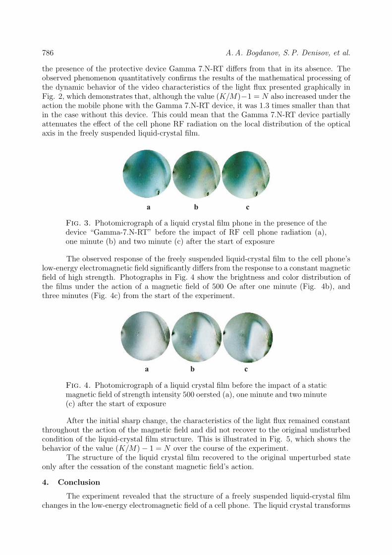
786 A.A. Bogdanov, S. P. Denisov, et al.
the presence of the protective device Gamma 7.N-RT differs from that in its absence. Theobserved phenomenon quantitatively confirms the results of the mathematical processing ofthe dynamic behavior of the video characteristics of the light flux presented graphically inFig. 2, which demonstrates that, although the value (K/M)−1 = N also increased under theaction the mobile phone with the Gamma 7.N-RT device, it was 1.3 times smaller than thatin the case without this device. This could mean that the Gamma 7.N-RT device partiallyattenuates the effect of the cell phone RF radiation on the local distribution of the opticalaxis in the freely suspended liquid-crystal film.
a b c
Fig. 3. Photomicrograph of a liquid crystal film phone in the presence of thedevice “Gamma-7.N-RT” before the impact of RF cell phone radiation (a),one minute (b) and two minute (c) after the start of exposure
The observed response of the freely suspended liquid-crystal film to the cell phone’slow-energy electromagnetic field significantly differs from the response to a constant magneticfield of high strength. Photographs in Fig. 4 show the brightness and color distribution ofthe films under the action of a magnetic field of 500 Oe after one minute (Fig. 4b), andthree minutes (Fig. 4c) from the start of the experiment.
a b c
Fig. 4. Photomicrograph of a liquid crystal film before the impact of a staticmagnetic field of strength intensity 500 oersted (a), one minute and two minute(c) after the start of exposure
After the initial sharp change, the characteristics of the light flux remained constantthroughout the action of the magnetic field and did not recover to the original undisturbedcondition of the liquid-crystal film structure. This is illustrated in Fig. 5, which shows thebehavior of the value (K/M)− 1 = N over the course of the experiment.
The structure of the liquid crystal film recovered to the original unperturbed stateonly after the cessation of the constant magnetic field’s action.
4. Conclusion
The experiment revealed that the structure of a freely suspended liquid-crystal filmchanges in the low-energy electromagnetic field of a cell phone. The liquid crystal transforms
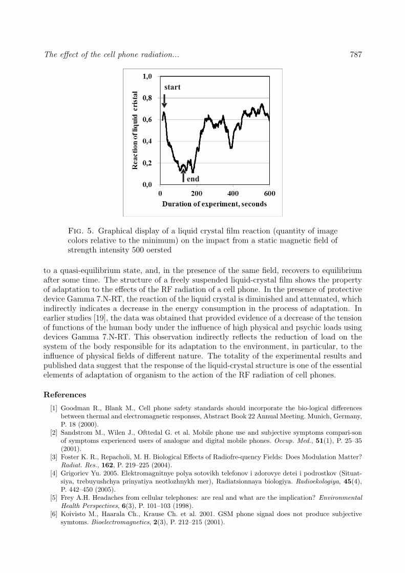
The effect of the cell phone radiation... 787
start
end
Fig. 5. Graphical display of a liquid crystal film reaction (quantity of imagecolors relative to the minimum) on the impact from a static magnetic field ofstrength intensity 500 oersted
to a quasi-equilibrium state, and, in the presence of the same field, recovers to equilibriumafter some time. The structure of a freely suspended liquid-crystal film shows the propertyof adaptation to the effects of the RF radiation of a cell phone. In the presence of protectivedevice Gamma 7.N-RT, the reaction of the liquid crystal is diminished and attenuated, whichindirectly indicates a decrease in the energy consumption in the process of adaptation. Inearlier studies [19], the data was obtained that provided evidence of a decrease of the tensionof functions of the human body under the influence of high physical and psychic loads usingdevices Gamma 7.N-RT. This observation indirectly reflects the reduction of load on thesystem of the body responsible for its adaptation to the environment, in particular, to theinfluence of physical fields of different nature. The totality of the experimental results andpublished data suggest that the response of the liquid-crystal structure is one of the essentialelements of adaptation of organism to the action of the RF radiation of cell phones.
References
[1] Goodman R., Blank M., Cell phone safety standards should incorporate the bio-logical differencesbetween thermal and electromagnetic responses, Abstract Book 22 Annual Meeting. Munich, Germany,P. 18 (2000).
[2] Sandstrom M., Wilen J., Ofttedal G. et al. Mobile phone use and subjective symptoms compari-sonof symptoms experienced users of analogue and digital mobile phones. Occup. Med., 51(1), P. 25–35(2001).
[3] Foster K. R., Repacholi, M. H. Biological Effects of Radiofre-quency Fields: Does Modulation Matter?Radiat. Res., 162, P. 219–225 (2004).
[4] Grigoriev Yu. 2005. Elektromagnitnye polya sotovikh telefonov i zdorovye detei i podrostkov (Situat-siya, trebuyushchya prinyatiya neotlozhnykh mer), Radiatsionnaya biologiya. Radioekologiya, 45(4),P. 442–450 (2005).
[5] Frey A.H. Headaches from cellular telephones: are real and what are the implication? EnvironmentalHealth Perspectives, 6(3), P. 101–103 (1998).
[6] Koivisto M., Haarala Ch., Krause Ch. et al. 2001. GSM phone signal does not produce subjectivesymtoms. Bioelectromagnetics, 2(3), P. 212–215 (2001).
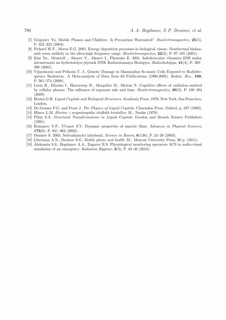
788 A.A. Bogdanov, S. P. Denisov, et al.
[7] Grigoriev Yu. Mobile Phones and Children: Is Precaution Warranted? Bioelectromagnetics, 25(5),P. 322–323 (2004).
[8] Pickard W.F., Moros E.G. 2001. Energy deposition processes in biological, tissue: Nonthermal biohaz-ards seem unlikely in the ultra-high frequency range. Bioelectromagnetics, 22(2), P. 97–105 (2001).
[9] Kim Yu., Montrell ., Akoyev V., Akoyev I., Phesenko E. 2001. Issledova-niye vliyaniya EMI maloyintensivnosti na hydrotatsiyu plyenok DNK Radiatsionnaya Biologiya. Radioekologiya, 41(4), P. 395–398 (2001).
[10] Vijayalaxmi and Prihoda T. J., Genetic Damage in Mammalian So-matic Cells Exposed to Radiofre-quency Radiation: A Meta-analysis of Data from 63 Publications (1990-2005). Radiat. Res., 169,P. 561–574 (2008).
[11] Luria R., Eliyahu I., Hareuveny R., Margaliot M., Meiran N. Cognitive effects of radiation emittedby cellular phones: The influence of exposure side and time. Bioelectromagnetics, 30(3), P. 198–204(2009).
[12] Brawn G.H. Liquid Crystals and Biological Structures. Academic Press, 1979, New York, San Francisco,London.
[13] De Gennes P.G. and Prost J. The Physics of Liquid Crystals. Clarendon Press, Oxford, p. 597 (1993).[14] Blinov L.M. Electro- i magnitooptika zhidkikh kristallov. M.: Nauka (1978).[15] Pikin S.A. Structural Transformations in Liquid Crystals. Gordon and Breach Science Publishers
(1991).[16] Romanov V.P., Ul’anov S.V. Dynamic properties of smectic films. Advances in Physical Sciences,
173(6), P. 941–963 (2003).[17] Denisov S. 2003. Neitralizatotri izluchenii. Science in Russia, 6(138), P. 24–26 (2003).[18] Liberman A.N., Denisov S.G. Mobile phone and health. M.: Moscow University Press, 90 p. (2011).[19] Aleksanin S.S., Bogdanov A.A., Zagarov E.S. Physiological monitoring operators ACS in audio-visual
simulation of an emergency. Radiation Hygiene, 3(3), P. 43–46 (2010).
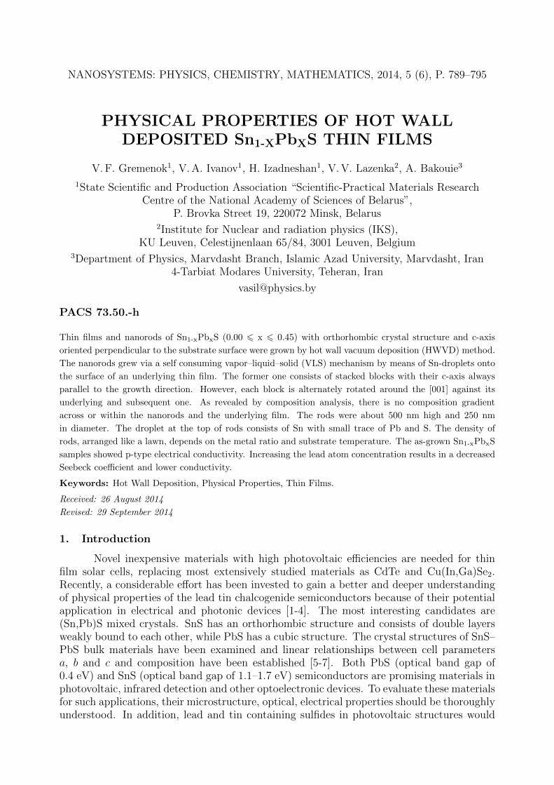
NANOSYSTEMS: PHYSICS, CHEMISTRY, MATHEMATICS, 2014, 5 (6), P. 789–795
PHYSICAL PROPERTIES OF HOT WALLDEPOSITED Sn1-XPbXS THIN FILMS
V. F. Gremenok1, V. A. Ivanov1, H. Izadneshan1, V. V. Lazenka2, A. Bakouie3
1State Scientific and Production Association “Scientific-Practical Materials ResearchCentre of the National Academy of Sciences of Belarus”,
P. Brovka Street 19, 220072 Minsk, Belarus2Institute for Nuclear and radiation physics (IKS),
KU Leuven, Celestijnenlaan 65/84, 3001 Leuven, Belgium3Department of Physics, Marvdasht Branch, Islamic Azad University, Marvdasht, Iran
4-Tarbiat Modares University, Teheran, Iran
PACS 73.50.-h
Thin films and nanorods of Sn1-xPbxS (0.00 6 x 6 0.45) with orthorhombic crystal structure and c-axis
oriented perpendicular to the substrate surface were grown by hot wall vacuum deposition (HWVD) method.
The nanorods grew via a self consuming vapor–liquid–solid (VLS) mechanism by means of Sn-droplets onto
the surface of an underlying thin film. The former one consists of stacked blocks with their c-axis always
parallel to the growth direction. However, each block is alternately rotated around the [001] against its
underlying and subsequent one. As revealed by composition analysis, there is no composition gradient
across or within the nanorods and the underlying film. The rods were about 500 nm high and 250 nm
in diameter. The droplet at the top of rods consists of Sn with small trace of Pb and S. The density of
rods, arranged like a lawn, depends on the metal ratio and substrate temperature. The as-grown Sn1-xPbxS
samples showed p-type electrical conductivity. Increasing the lead atom concentration results in a decreased
Seebeck coefficient and lower conductivity.
Keywords: Hot Wall Deposition, Physical Properties, Thin Films.
Received: 26 August 2014
Revised: 29 September 2014
1. Introduction
Novel inexpensive materials with high photovoltaic efficiencies are needed for thinfilm solar cells, replacing most extensively studied materials as CdTe and Cu(In,Ga)Se2.Recently, a considerable effort has been invested to gain a better and deeper understandingof physical properties of the lead tin chalcogenide semiconductors because of their potentialapplication in electrical and photonic devices [1-4]. The most interesting candidates are(Sn,Pb)S mixed crystals. SnS has an orthorhombic structure and consists of double layersweakly bound to each other, while PbS has a cubic structure. The crystal structures of SnS–PbS bulk materials have been examined and linear relationships between cell parametersa, b and c and composition have been established [5-7]. Both PbS (optical band gap of0.4 eV) and SnS (optical band gap of 1.1–1.7 eV) semiconductors are promising materials inphotovoltaic, infrared detection and other optoelectronic devices. To evaluate these materialsfor such applications, their microstructure, optical, electrical properties should be thoroughlyunderstood. In addition, lead and tin containing sulfides in photovoltaic structures would

790 V. F. Gremenok, V. A. Ivanov, et al.
decrease the production costs of solar cells, because the materials involved are cost effective,abundant in nature, and somewhat less-toxic.
A few techniques have been applied for the preparation of Sn1-xPbxS thin films. Thefirst report was by Thangaraju and co-workers [8], who prepared PbSnS2 films by a spraypyrolysis method. Unuchak et al. deposited PbSnS2 thin film by thermal evaporation [4].The preliminary structural and optical characteristics have been reported.
New approaches and various techniques must be developed to control the deposi-tion of photoactive materials with minimum density of defects, so that carrier generation,transport, and collection are optimized. Shape and size of nanostructures have considerableinfluence on physical properties of such semiconductors especially for the phonons due to thelattice part of the thermal conductivity for which nanorods constitute an important classof corresponding 1D nanostructures [9-11]. At the same time, bicontinuous morphology isnecessary to decrease the distance needed for excitons to diffuse to interfaces and to allowcharges to efficiently diffuse to electrode interfaces. Nanorods constitute an important classof 1D nanostructure and can also act as active components in devices. Previously, mucheffort has been made to develop novel methods for fabrication of nanostructured chalco-genide semiconductors [12]. Among these technologies, the vapor-liquid-solid (VLS) methodseems to be the most successful for generating nanocrystalline nanowires with relatively largequantities [13,14].
In our continuing effort to prepare the SnS–PbS semiconductor films, we have useda hot wall vacuum deposition (HWVD) method. Among the various thin films depositiontechniques, HWVD has become a popular and reliable synthesis for films preparation [15-21].This deposition technology yields high quality thin films with smooth surfaces grown underconditions very close to a quasi thermal equilibrium. The high quality of the electrical andoptical properties thin films of the different II-VI materials produced by this method didn’trequire additional post-growth heat treatments [22,23].
Here, we report on the preparation of Sn1-xPbxS thin films and nanorods by thehot wall vacuum deposition of bulk materials onto glass substrates using different syntheticparameters. Microstructure and electrical properties of the as deposited materials are alsodescribed.
2. Experimental details
The polycrystalline Sn1-xPbxS (0.00 6 x 6 0.45) ingots used as targets were syn-thesized by reaction of Sn, S of high purity 99.999% and natural galena (PbS) containing0.04 at.% Ag and Sb, 0.06 at.% Cu, 0.07 at.% Zn, and 0.08 at.% Au in silica ampoules. Mix-tures of constituent elements in stoichiometric proportions (with an accuracy of 5×10⁻⁷ kg)were sealed into evacuated ampoules at the pressure of 10−3 Torr. The evacuated tube wasthen placed into an electric furnace and kept at 730 K for 7 days and after that at 970 K for10 days. In order to avoid explosions due to the sulfur vapor pressure, the tube was heatedslowly (300 K/h). The tubes were cooled gradually, with a cooling rate of about 295 K/h toroom temperature in order to obtain polycrystalline Sn1-xPbxS compounds.
The main feature of the hot wall deposition system is the heated linear quartz tubeof 1.2×10⁻² m diameter, which served to enclose and direct the vapor from the source tothe substrate. The quartz tube and substrates were heated independently. The quartz tubewas charged with Sn1-xPbxS powder and the films were deposited by keeping the quartz tubetemperatures around 870 K. Glass plates were chemically cleaned, rinsed with distilled waterbefore deposition. Substrate temperature was varied from 520 to 680 K. The substrate washeld at a distance of about 10−4 m above the open end of the quartz tube acting almost
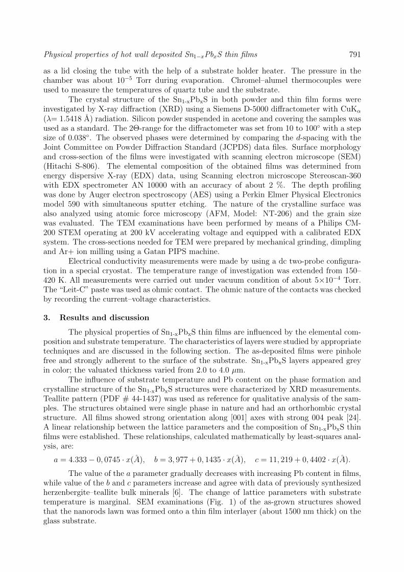
Physical properties of hot wall deposited Sn1−xPbxS thin films 791
as a lid closing the tube with the help of a substrate holder heater. The pressure in thechamber was about 10−5 Torr during evaporation. Chromel–alumel thermocouples wereused to measure the temperatures of quartz tube and the substrate.
The crystal structure of the Sn1-xPbxS in both powder and thin film forms wereinvestigated by X-ray diffraction (XRD) using a Siemens D-5000 diffractometer with CuKα
(λ= 1.5418 A) radiation. Silicon powder suspended in acetone and covering the samples wasused as a standard. The 2Θ-range for the diffractometer was set from 10 to 100 with a stepsize of 0.038. The observed phases were determined by comparing the d-spacing with theJoint Committee on Powder Diffraction Standard (JCPDS) data files. Surface morphologyand cross-section of the films were investigated with scanning electron microscope (SEM)(Hitachi S-806). The elemental composition of the obtained films was determined fromenergy dispersive X-ray (EDX) data, using Scanning electron microscope Stereoscan-360with EDX spectrometer AN 10000 with an accuracy of about 2 %. The depth profilingwas done by Auger electron spectroscopy (AES) using a Perkin Elmer Physical Electronicsmodel 590 with simultaneous sputter etching. The nature of the crystalline surface wasalso analyzed using atomic force microscopy (AFM, Model: NT-206) and the grain sizewas evaluated. The TEM examinations have been performed by means of a Philips CM-200 STEM operating at 200 kV accelerating voltage and equipped with a calibrated EDXsystem. The cross-sections needed for TEM were prepared by mechanical grinding, dimplingand Ar+ ion milling using a Gatan PIPS machine.
Electrical conductivity measurements were made by using a dc two-probe configura-tion in a special cryostat. The temperature range of investigation was extended from 150–420 K. All measurements were carried out under vacuum condition of about 5×10⁻⁴ Torr.The “Leit-C” paste was used as ohmic contact. The ohmic nature of the contacts was checkedby recording the current–voltage characteristics.
3. Results and discussion
The physical properties of Sn1-xPbxS thin films are influenced by the elemental com-position and substrate temperature. The characteristics of layers were studied by appropriatetechniques and are discussed in the following section. The as-deposited films were pinholefree and strongly adherent to the surface of the substrate. Sn1-xPbxS layers appeared greyin color; the valuated thickness varied from 2.0 to 4.0 µm.
The influence of substrate temperature and Pb content on the phase formation andcrystalline structure of the Sn1-xPbxS structures were characterized by XRD measurements.Teallite pattern (PDF # 44-1437) was used as reference for qualitative analysis of the sam-ples. The structures obtained were single phase in nature and had an orthorhombic crystalstructure. All films showed strong orientation along [001] axes with strong 004 peak [24].A linear relationship between the lattice parameters and the composition of Sn1-xPbxS thinfilms were established. These relationships, calculated mathematically by least-squares anal-ysis, are:
a = 4.333 − 0, 0745 · x(A), b = 3, 977 + 0, 1435 · x(A), c = 11, 219 + 0, 4402 · x(A).
The value of the a parameter gradually decreases with increasing Pb content in films,while value of the b and c parameters increase and agree with data of previously synthesizedherzenbergite–teallite bulk minerals [6]. The change of lattice parameters with substratetemperature is marginal. SEM examinations (Fig. 1) of the as-grown structures showedthat the nanorods lawn was formed onto a thin film interlayer (about 1500 nm thick) on theglass substrate.
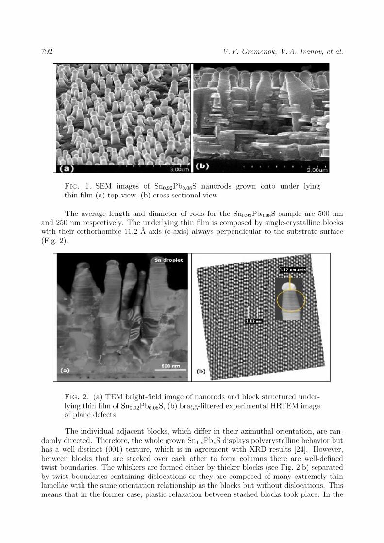
792 V. F. Gremenok, V. A. Ivanov, et al.
Fig. 1. SEM images of Sn0.92Pb0.08S nanorods grown onto under lyingthin film (a) top view, (b) cross sectional view
The average length and diameter of rods for the Sn0.92Pb0.08S sample are 500 nmand 250 nm respectively. The underlying thin film is composed by single-crystalline blockswith their orthorhombic 11.2 A axis (c-axis) always perpendicular to the substrate surface(Fig. 2).
Fig. 2. (a) TEM bright-field image of nanorods and block structured under-lying thin film of Sn0.92Pb0.08S, (b) bragg-filtered experimental HRTEM imageof plane defects
The individual adjacent blocks, which differ in their azimuthal orientation, are ran-domly directed. Therefore, the whole grown Sn1-xPbxS displays polycrystalline behavior buthas a well-distinct (001) texture, which is in agreement with XRD results [24]. However,between blocks that are stacked over each other to form columns there are well-definedtwist boundaries. The whiskers are formed either by thicker blocks (see Fig. 2,b) separatedby twist boundaries containing dislocations or they are composed of many extremely thinlamellae with the same orientation relationship as the blocks but without dislocations. Thismeans that in the former case, plastic relaxation between stacked blocks took place. In the
Physical properties of hot wall deposited Sn1−xPbxS thin films 793
latter one, pseudomorphic intergrowth between stacked thin strained lamellae occurs, i.e.,there is elastic relaxation without forming dislocations. As revealed by TEM-EDX analysis,the average composition of the blocks and rods is the same without any composition gradientacross the whole Sn1-xPbxS sample structure (Fig. 3). As seen from the Fig. 1 and Fig. 2the droplets were formed at the tip of the rods. TEM-EDX experiments showed that thesedroplets consist of Sn and about 0.6 at.% Pb and 1.2 at.% S.
Fig. 3. Compositional distribution along Sn0.9Pb0.1S sample determined bycalibrated TEM-EDX. The points for quantitative TEM-EDX measurementsare indicated by 1 to 16
It was suggested that these droplets are liquid at growth temperature and act asa solute for the sulfur and lead, and tin may also come from the vapor phase during thegrowth process. Therefore, it is assumed the rods grew via a self-consuming vapor–liquid–solid (VLS) mechanism [13-14].
The experiments confirm that the nanorod growth depends strongly on the lead con-centration and substrate temperature. The lawn of nanorods with lead concentration rangingfrom 4 at.% to 6 at.% was formed onto the underlying Sn1-xPbxS thin film at substrate tem-peratures of 570–590 K. Thin films containing ca. 8 at.% Pb grown on glass at temperaturesless then 540 K have few droplets on their surfaces only (Fig. 4).
At a substrate temperature of 600 K, the droplets required for VLS growth begin toform (Fig. 4b) and at 630 K an array of whiskers 500 nm high and 250 nm in diameter can beobserved (Figs. 4c). However, at substrate temperatures of 670 K and higher, lawn-growthcould not be found even though some few droplets and single nanorods appeared. Thus,it can be concluded that for higher Pb content, higher substrate temperatures are requiredto produce nanorods. The as-grown Sn1-xPbxS films showed p-type electrical conductiv-ity, which is confirmed by the thermoelectric probe measurement. The Seebeck coefficientand conductivity of the layers was in the range of α = 6-360 µV/K and σ = 4.8×10⁻⁵
– 1.5×10⁻²Ω−1·cm−1 respectively at room temperature, depending on concentration of thelead in the films.
An increase of the Pb concentration leads to a decrease of the Seebeck coefficientand decrease of conductivity [4]. If Na deriving from diffusion from the glass substrate is
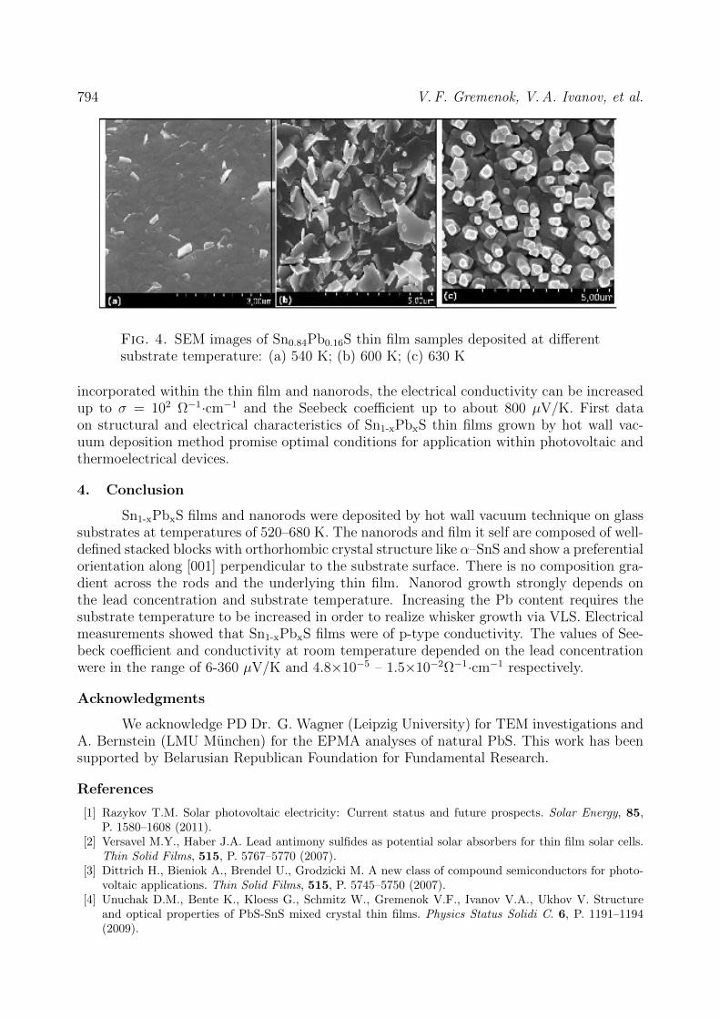
794 V. F. Gremenok, V. A. Ivanov, et al.
Fig. 4. SEM images of Sn0.84Pb0.16S thin film samples deposited at differentsubstrate temperature: (a) 540 K; (b) 600 K; (c) 630 K
incorporated within the thin film and nanorods, the electrical conductivity can be increasedup to σ = 102 Ω−1·cm−1 and the Seebeck coefficient up to about 800 µV/K. First dataon structural and electrical characteristics of Sn1-xPbxS thin films grown by hot wall vac-uum deposition method promise optimal conditions for application within photovoltaic andthermoelectrical devices.
4. Conclusion
Sn1-xPbxS films and nanorods were deposited by hot wall vacuum technique on glasssubstrates at temperatures of 520–680 K. The nanorods and film it self are composed of well-defined stacked blocks with orthorhombic crystal structure like α–SnS and show a preferentialorientation along [001] perpendicular to the substrate surface. There is no composition gra-dient across the rods and the underlying thin film. Nanorod growth strongly depends onthe lead concentration and substrate temperature. Increasing the Pb content requires thesubstrate temperature to be increased in order to realize whisker growth via VLS. Electricalmeasurements showed that Sn1-xPbxS films were of p-type conductivity. The values of See-beck coefficient and conductivity at room temperature depended on the lead concentrationwere in the range of 6-360 µV/K and 4.8×10⁻⁵ – 1.5×10⁻²Ω−1·cm−1 respectively.
Acknowledgments
We acknowledge PD Dr. G. Wagner (Leipzig University) for TEM investigations andA. Bernstein (LMU Munchen) for the EPMA analyses of natural PbS. This work has beensupported by Belarusian Republican Foundation for Fundamental Research.
References
[1] Razykov T.M. Solar photovoltaic electricity: Current status and future prospects. Solar Energy, 85,P. 1580–1608 (2011).
[2] Versavel M.Y., Haber J.A. Lead antimony sulfides as potential solar absorbers for thin film solar cells.Thin Solid Films, 515, P. 5767–5770 (2007).
[3] Dittrich H., Bieniok A., Brendel U., Grodzicki M. A new class of compound semiconductors for photo-voltaic applications. Thin Solid Films, 515, P. 5745–5750 (2007).
[4] Unuchak D.M., Bente K., Kloess G., Schmitz W., Gremenok V.F., Ivanov V.A., Ukhov V. Structureand optical properties of PbS-SnS mixed crystal thin films. Physics Status Solidi C. 6, P. 1191–1194(2009).
Physical properties of hot wall deposited Sn1−xPbxS thin films 795
[5] Krebs H. and Langner D. Uber struktur und eigenschaften der halbmetalle. XVI. Mischkristallsystemezwischen halbleitenden chalkogeniden der vierten hauptgruppe. Zeitschrift fur anorganische und allge-meine Chemie, 334, P. 37–49 (1964).
[6] Hayashi K., Kitakaze A., Sugaki A. A re-examination of herzenbergite-teallite solid solution at temper-atures between 300 and 700C. Mineralogical Magazine, 65, P. 645–651 (2001).
[7] Lebedev A.I., Sluchinskaya I.A., Munro I.H, An EXAFS study of the local structure of the PbxSn1−xSsolid solution. Physics of the Solid State, 44, P. 1643–1647 (2002).
[8] Thangaraju B. and Kaliannan P. Polycrystalline Lead Tin Chalcogenide Thin Film Grown by SprayPyrolysis Crystal Research Technology, 35, P. 71–75 (2000).
[9] Lieber C.M. One-Dimensional Nanostructures: Chemistry, Physics & Applications. Solid State Com-munications, 107, P. 607–616 (1998).
[10] Manna L., Scher E.C., Alivisatos A.P. Synthesis of soluble and processable rod-, arrow-, teardrop-, andtetrapod-shaped CdSe nanocrystals. J. American Chemistry Society, 122, P. 12700–12706 (2000).
[11] Deng Z.X., Wang C., Sun X.M., Li Y.D. Structure-Directing Coordination Template Effect of Ethylene-diamine in Formations of ZnS and ZnSe Nanocrystallites via Solvothermal Route. Inorganic Chemistry,41, P. 869–873 (2002).
[12] Rao C.N., Deepak F.L., Gundiah. G., Govindaraj A. Inorganic nanowires. Progress Solid State Chem-istry, 31, P. 5–147 (2003).
[13] Xia Y.N., Yang P.D., Sun Y.G., Wu Y.Y., Mayers B., Gates B., Yin Y.D., Kim F., Yan H.Q. One-Dimensional Nanostructures: Synthesis, Characterization, and Applications. Advanced Materials, 15,P. 353–389 (2003).
[14] Wagner R.S., Ellis W.S. Vapor-liquid-solid mechanism of single crystal growth. Applied Physics Letters,4, P. 89–90 (1964).
[15] Lopez-Otero, A. Hot wall epitaxy. Thin Solid Films, 49, P. 3–57 (1978).[16] Chaudhuri S., Mondal A., Pal A.K. Structural studies of CdSe films deposited onto glass, NaCI and
substrates by a hot-wall technique. Journal of Materials Science Letters, 6, P. 366–369 (1987).[17] Seto S., Yamada S., Suzuki K. Growth kinetics and structural characterization of polycrystalline CdTe
films grown by hot-wall vacuum evaporation. Solar Energy Materials and Solar Cells, 50, P. 133–139(1998).
[18] Velumani S., Narayandass S.K., Mangalara D. Structural characterization of hot wall deposited cadmiumselenide thin films. Semiconductors Science and Technology, 13, P. 1016–1024 (1998).
[19] Velumani, S., Mathew, X., Sebastian, P.J. Thickness dependent properties of hot wall deposited CdSefilms. Journal of Materials Science Letters, 22, P. 25–28 (2003).
[20] Muthukumarasamy N., Balasundaraprabhu R., Jayakumar S., Kannan M.D. Photoconductive proper-ties of hot wall deposited CdSe0,6Te0,4 thin films. Materials Science and Engineering B, 137, P. 1–4(2007).
[21] Agilan S., Venkatachalam S., Mangalaraj D., Narayandass Sa.K., Velumani S., Singh Vijay P. Structuraland photoelectrical characterization of hot wall deposited CuInSe2 thin films and the fabrication ofCuInSe2 based solar cells. Materials Characterization, 58, P. 701–707 (2007).
[22] Schikora D., Sitter H., Humenberger J., Lischka K. High quality CdTe epilayers on GaAs grown byhotwall epitaxy. Applied Physics Letters, 48, P. 1276–1278 (1986).
[23] Pal A.K., Mondal A., Chaudhuri S. Preparation and characterization of ZnTe/CdSe solar cells. Vacuum,41, P. 1460–1462 (1990).
[24] Bente K, Lazenka V.V., Unuchak D.G., Wagner G., Gremenok V.F. Epitaxial Sn1−xPbxS nanorods oniso-compositional thin films, Crystal. Research Technology, 45, P. 643–646 (2010).
NANOSYSTEMS: PHYSICS, CHEMISTRY, MATHEMATICS, 2014, 5 (6), P. 796–802
FABRICATION AND CHARACTERIZATIONZnCdS NANOWIRE
M. A. Jafarov, E. F. Nasirov, R. Mammadov, R. Jafarli
Baku State University, Baku 1045, Z. Khalilov st. 23, Azerbaijan
PACS 71.55.Gs, 78.20.-e, 85.30.-z, 85.60.Dw
Semiconductor ZnCdS nanowire arrays have been synthesized by electrochemical deposition from aqueous solutions
into porous anodic alumina substrates. X-ray diffraction analyses show that the as-synthesized nanowires have a
highly preferential orientation. Scanning electron microscopy indicates that high-filling, ordered, and single-
crystalline nanowire arrays have been obtained. The optical absorption spectra of the nanowire arrays show that
the optical absorption band edge of the ZnCdS nanowire array exhibits a blue shift compared with that of bulk
ZnCdS. The growth mechanism and the electrochemical deposition process are discussed together with the chemical
compositions analysis.
Keywords: Nanowire, electrochemical deposition, nanoparticle, ZnCdS.
Received: 30 November 2014
1. Introduction
Sulfides or selenides, as wide-band gap II-VI semiconductor materials, have been stud-ied extensively due to their wide applications in the fields of light-emitting devices, solar cells,sensors, and optical recording materials [1–3]. ZnS is a wide band gap semiconductor, commer-cially used in a variety of applications, including optical coatings, solid-state solar cell windows,in thin film electroluminescent devices, photoconductors, field effect transistors, sensors, andlight-emitting applications. To date, there are many methodologies available for synthesizingZnS powders, such as laser ablation, electrochemical fabrication and solvothermal methods. Thesynthesis of ZnS nanowires, ZnS nanorods by a surfactant-assisted soft chemistry approach andZnS nanocrystals in colloids are all known methods.
One-dimensional (1D) semiconductor nanostructures have received much attention due totheir novel properties and potential applications in nanoscale electronics and optoelectronics [4,5]. Among these semiconductor systems, the II-VI family of the compound semiconductors,including ZnS, CdS, and CdTe, has been widely studied because of their potential applicationsin solar cells, photodetectors, and light emitting diodes [6,7]. Many attempts have been made tofabricate 1D nanostructures, such as high-temperature chemical vapor deposition (CVD) [8, 9],Among these methods, the anodic alumina substrate (AAS)-based synthesis is a widely usedroute for fabricating 1D nanostructures, because the AAS’s possess a uniform and parallel porousstructure, which can be used as templates to assemble high-quality nanowire and nanotubearrays [10, 11].
Cadmium sulfide (CdS), an important semiconductor material with a direct optical bandgap of 2.4 – 2.45 eV at room temperature, has potential applications in optoelectronic andthermoelectric devices. To the best of our knowledge, there are no reports on the fabrication ofthe CdS nanowire (NW) arrays.
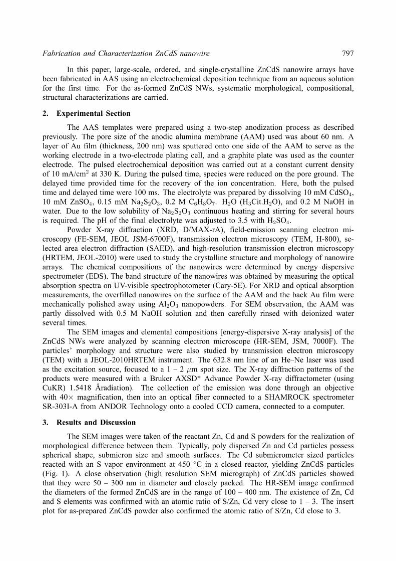
Fabrication and Characterization ZnCdS nanowire 797
In this paper, large-scale, ordered, and single-crystalline ZnCdS nanowire arrays havebeen fabricated in AAS using an electrochemical deposition technique from an aqueous solutionfor the first time. For the as-formed ZnCdS NWs, systematic morphological, compositional,structural characterizations are carried.
2. Experimental Section
The AAS templates were prepared using a two-step anodization process as describedpreviously. The pore size of the anodic alumina membrane (AAM) used was about 60 nm. Alayer of Au film (thickness, 200 nm) was sputtered onto one side of the AAM to serve as theworking electrode in a two-electrode plating cell, and a graphite plate was used as the counterelectrode. The pulsed electrochemical deposition was carried out at a constant current densityof 10 mA/cm2 at 330 K. During the pulsed time, species were reduced on the pore ground. Thedelayed time provided time for the recovery of the ion concentration. Here, both the pulsedtime and delayed time were 100 ms. The electrolyte was prepared by dissolving 10 mM CdSO4,10 mM ZnSO4, 0.15 mM Na2S2O3, 0.2 M C6H8O7. H2O (H3Cit.H2O), and 0.2 M NaOH inwater. Due to the low solubility of Na2S2O3 continuous heating and stirring for several hoursis required. The pH of the final electrolyte was adjusted to 3.5 with H2SO4.
Powder X-ray diffraction (XRD, D/MAX-rA), field-emission scanning electron mi-croscopy (FE-SEM, JEOL JSM-6700F), transmission electron microscopy (TEM, H-800), se-lected area electron diffraction (SAED), and high-resolution transmission electron microscopy(HRTEM, JEOL-2010) were used to study the crystalline structure and morphology of nanowirearrays. The chemical compositions of the nanowires were determined by energy dispersivespectrometer (EDS). The band structure of the nanowires was obtained by measuring the opticalabsorption spectra on UV-visible spectrophotometer (Cary-5E). For XRD and optical absorptionmeasurements, the overfilled nanowires on the surface of the AAM and the back Au film weremechanically polished away using Al2O3 nanopowders. For SEM observation, the AAM waspartly dissolved with 0.5 M NaOH solution and then carefully rinsed with deionized waterseveral times.
The SEM images and elemental compositions [energy-dispersive X-ray analysis] of theZnCdS NWs were analyzed by scanning electron microscope (HR-SEM, JSM, 7000F). Theparticles’ morphology and structure were also studied by transmission electron microscopy(TEM) with a JEOL-2010HRTEM instrument. The 632.8 nm line of an He–Ne laser was usedas the excitation source, focused to a 1 – 2 µm spot size. The X-ray diffraction patterns of theproducts were measured with a Bruker AXSD* Advance Powder X-ray diffractometer (usingCuKR) 1.5418 Aradiation). The collection of the emission was done through an objectivewith 40× magnification, then into an optical fiber connected to a SHAMROCK spectrometerSR-303I-A from ANDOR Technology onto a cooled CCD camera, connected to a computer.
3. Results and Discussion
The SEM images were taken of the reactant Zn, Cd and S powders for the realization ofmorphological difference between them. Typically, poly dispersed Zn and Cd particles possessspherical shape, submicron size and smooth surfaces. The Cd submicrometer sized particlesreacted with an S vapor environment at 450 C in a closed reactor, yielding ZnCdS particles(Fig. 1). A close observation (high resolution SEM micrograph) of ZnCdS particles showedthat they were 50 – 300 nm in diameter and closely packed. The HR-SEM image confirmedthe diameters of the formed ZnCdS are in the range of 100 – 400 nm. The existence of Zn, Cdand S elements was confirmed with an atomic ratio of S/Zn, Cd very close to 1 – 3. The insertplot for as-prepared ZnCdS powder also confirmed the atomic ratio of S/Zn, Cd close to 3.

798 M. A. Jafarov, E. F. Nasirov, R. Mammadov, R. Jafarli
Figure 1 shows the XRD pattern of the as-prepared ZnCdS nanowire array. The inten-sity of the (220) diffraction is much higher than all the other peaks, indicating that the ZnCdSnanowires have a preferential orientation along the [220] direction, which will be further con-formed by HRTEM analysis. In addition, no diffraction peaks for elemental Cd and S can bedetected.
FIG. 1. XRD pattern of ZnCdS nanowire array
Figure 2 shows the dependence of the (220) peak intensity of XRD patterns of theZnCdS nanowires on the current density and pulsed time. One can see that the peak intensityfirst increases, after reaching a maximum value at the current density of 10 mA/cm2, and thendecreases with further increasing of the current density.
FIG. 2. Relative intensity of the (220) peak of ZnCdS nanowires as a functionof (a) current density (I) and (b) pulsed time (t), keeping the delayed time at100 ms
The reduction in the peak intensity might be due to hydrogen evolution at larger currentdensities, which suppresses the growth of the nanowires along the (220) orientation. Keeping
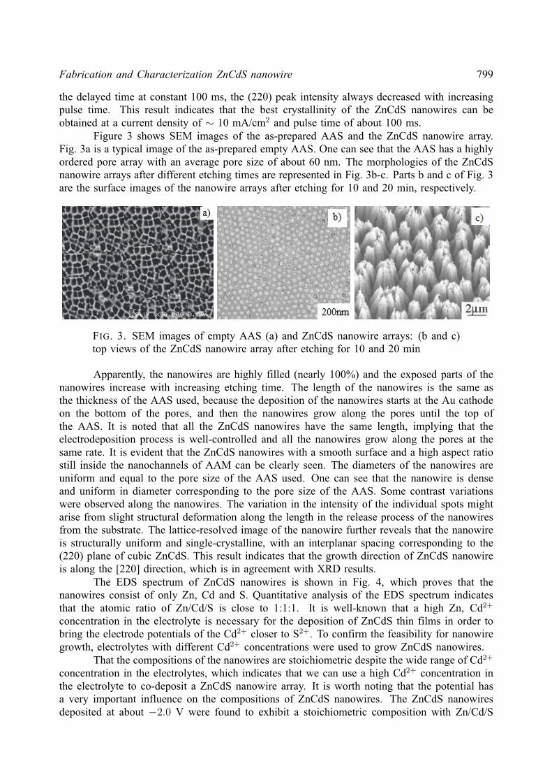
Fabrication and Characterization ZnCdS nanowire 799
the delayed time at constant 100 ms, the (220) peak intensity always decreased with increasingpulse time. This result indicates that the best crystallinity of the ZnCdS nanowires can beobtained at a current density of ∼ 10 mA/cm2 and pulse time of about 100 ms.
Figure 3 shows SEM images of the as-prepared AAS and the ZnCdS nanowire array.Fig. 3a is a typical image of the as-prepared empty AAS. One can see that the AAS has a highlyordered pore array with an average pore size of about 60 nm. The morphologies of the ZnCdSnanowire arrays after different etching times are represented in Fig. 3b-c. Parts b and c of Fig. 3are the surface images of the nanowire arrays after etching for 10 and 20 min, respectively.
FIG. 3. SEM images of empty AAS (a) and ZnCdS nanowire arrays: (b and c)top views of the ZnCdS nanowire array after etching for 10 and 20 min
Apparently, the nanowires are highly filled (nearly 100%) and the exposed parts of thenanowires increase with increasing etching time. The length of the nanowires is the same asthe thickness of the AAS used, because the deposition of the nanowires starts at the Au cathodeon the bottom of the pores, and then the nanowires grow along the pores until the top ofthe AAS. It is noted that all the ZnCdS nanowires have the same length, implying that theelectrodeposition process is well-controlled and all the nanowires grow along the pores at thesame rate. It is evident that the ZnCdS nanowires with a smooth surface and a high aspect ratiostill inside the nanochannels of AAM can be clearly seen. The diameters of the nanowires areuniform and equal to the pore size of the AAS used. One can see that the nanowire is denseand uniform in diameter corresponding to the pore size of the AAS. Some contrast variationswere observed along the nanowires. The variation in the intensity of the individual spots mightarise from slight structural deformation along the length in the release process of the nanowiresfrom the substrate. The lattice-resolved image of the nanowire further reveals that the nanowireis structurally uniform and single-crystalline, with an interplanar spacing corresponding to the(220) plane of cubic ZnCdS. This result indicates that the growth direction of ZnCdS nanowireis along the [220] direction, which is in agreement with XRD results.
The EDS spectrum of ZnCdS nanowires is shown in Fig. 4, which proves that thenanowires consist of only Zn, Cd and S. Quantitative analysis of the EDS spectrum indicatesthat the atomic ratio of Zn/Cd/S is close to 1:1:1. It is well-known that a high Zn, Cd2+
concentration in the electrolyte is necessary for the deposition of ZnCdS thin films in order tobring the electrode potentials of the Cd2+ closer to S2+. To confirm the feasibility for nanowiregrowth, electrolytes with different Cd2+ concentrations were used to grow ZnCdS nanowires.
That the compositions of the nanowires are stoichiometric despite the wide range of Cd2+
concentration in the electrolytes, which indicates that we can use a high Cd2+ concentration inthe electrolyte to co-deposit a ZnCdS nanowire array. It is worth noting that the potential hasa very important influence on the compositions of ZnCdS nanowires. The ZnCdS nanowiresdeposited at about −2.0 V were found to exhibit a stoichiometric composition with Zn/Cd/S
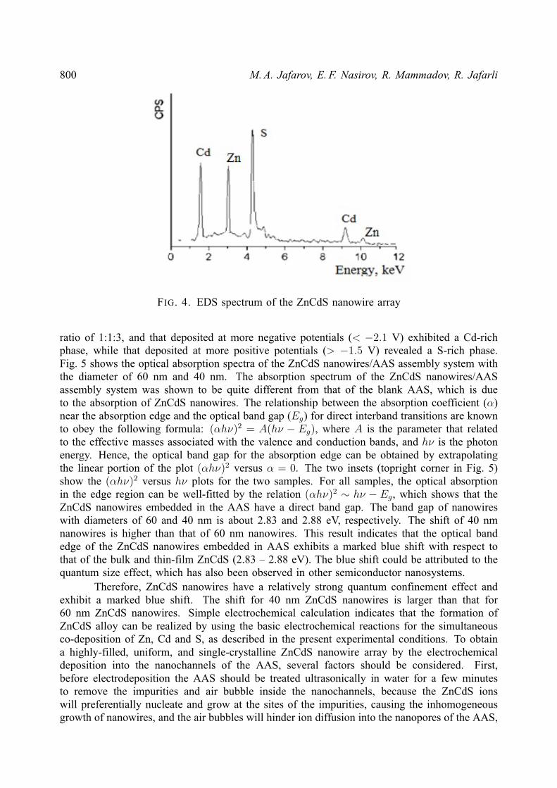
800 M. A. Jafarov, E. F. Nasirov, R. Mammadov, R. Jafarli
FIG. 4. EDS spectrum of the ZnCdS nanowire array
ratio of 1:1:3, and that deposited at more negative potentials (< −2.1 V) exhibited a Cd-richphase, while that deposited at more positive potentials (> −1.5 V) revealed a S-rich phase.Fig. 5 shows the optical absorption spectra of the ZnCdS nanowires/AAS assembly system withthe diameter of 60 nm and 40 nm. The absorption spectrum of the ZnCdS nanowires/AASassembly system was shown to be quite different from that of the blank AAS, which is dueto the absorption of ZnCdS nanowires. The relationship between the absorption coefficient (α)near the absorption edge and the optical band gap (Eg) for direct interband transitions are knownto obey the following formula: (αhν)2 = A(hν − Eg), where A is the parameter that relatedto the effective masses associated with the valence and conduction bands, and hν is the photonenergy. Hence, the optical band gap for the absorption edge can be obtained by extrapolatingthe linear portion of the plot (αhν)2 versus α = 0. The two insets (topright corner in Fig. 5)show the (αhν)2 versus hν plots for the two samples. For all samples, the optical absorptionin the edge region can be well-fitted by the relation (αhν)2 ∼ hν − Eg, which shows that theZnCdS nanowires embedded in the AAS have a direct band gap. The band gap of nanowireswith diameters of 60 and 40 nm is about 2.83 and 2.88 eV, respectively. The shift of 40 nmnanowires is higher than that of 60 nm nanowires. This result indicates that the optical bandedge of the ZnCdS nanowires embedded in AAS exhibits a marked blue shift with respect tothat of the bulk and thin-film ZnCdS (2.83 – 2.88 eV). The blue shift could be attributed to thequantum size effect, which has also been observed in other semiconductor nanosystems.
Therefore, ZnCdS nanowires have a relatively strong quantum confinement effect andexhibit a marked blue shift. The shift for 40 nm ZnCdS nanowires is larger than that for60 nm ZnCdS nanowires. Simple electrochemical calculation indicates that the formation ofZnCdS alloy can be realized by using the basic electrochemical reactions for the simultaneousco-deposition of Zn, Cd and S, as described in the present experimental conditions. To obtaina highly-filled, uniform, and single-crystalline ZnCdS nanowire array by the electrochemicaldeposition into the nanochannels of the AAS, several factors should be considered. First,before electrodeposition the AAS should be treated ultrasonically in water for a few minutesto remove the impurities and air bubble inside the nanochannels, because the ZnCdS ionswill preferentially nucleate and grow at the sites of the impurities, causing the inhomogeneousgrowth of nanowires, and the air bubbles will hinder ion diffusion into the nanopores of the AAS,
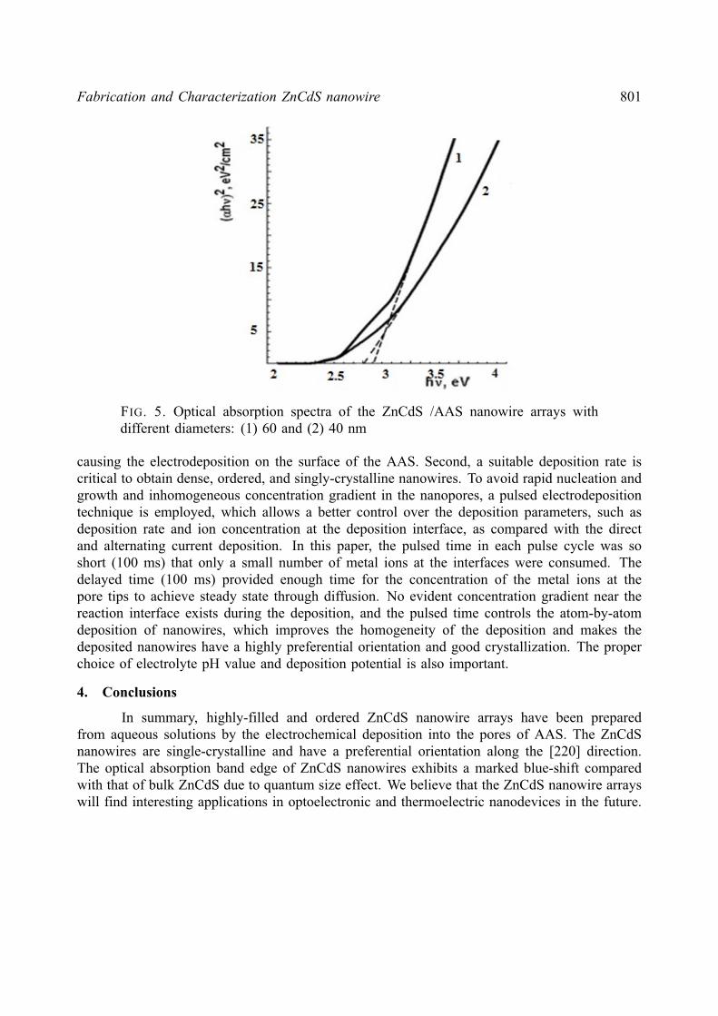
Fabrication and Characterization ZnCdS nanowire 801
FIG. 5. Optical absorption spectra of the ZnCdS /AAS nanowire arrays withdifferent diameters: (1) 60 and (2) 40 nm
causing the electrodeposition on the surface of the AAS. Second, a suitable deposition rate iscritical to obtain dense, ordered, and singly-crystalline nanowires. To avoid rapid nucleation andgrowth and inhomogeneous concentration gradient in the nanopores, a pulsed electrodepositiontechnique is employed, which allows a better control over the deposition parameters, such asdeposition rate and ion concentration at the deposition interface, as compared with the directand alternating current deposition. In this paper, the pulsed time in each pulse cycle was soshort (100 ms) that only a small number of metal ions at the interfaces were consumed. Thedelayed time (100 ms) provided enough time for the concentration of the metal ions at thepore tips to achieve steady state through diffusion. No evident concentration gradient near thereaction interface exists during the deposition, and the pulsed time controls the atom-by-atomdeposition of nanowires, which improves the homogeneity of the deposition and makes thedeposited nanowires have a highly preferential orientation and good crystallization. The properchoice of electrolyte pH value and deposition potential is also important.
4. Conclusions
In summary, highly-filled and ordered ZnCdS nanowire arrays have been preparedfrom aqueous solutions by the electrochemical deposition into the pores of AAS. The ZnCdSnanowires are single-crystalline and have a preferential orientation along the [220] direction.The optical absorption band edge of ZnCdS nanowires exhibits a marked blue-shift comparedwith that of bulk ZnCdS due to quantum size effect. We believe that the ZnCdS nanowire arrayswill find interesting applications in optoelectronic and thermoelectric nanodevices in the future.
802 M. A. Jafarov, E. F. Nasirov, R. Mammadov, R. Jafarli
References
[1] Wang Y.B., Wang Y.S., Xu R. Photochemical deposition of Pt on CdS for H2 evolution from water: markedlyenhanced activity by controlling Pt reduction environment. J. Phys. Chem. C, 117, P. 783–790 (2013).
[2] Bai Y., et al. In situ growth of a ZnO nanowire network within a TiO2 nanoparticle film for enhanceddye-sensitized solar cell performance. Adv. Mater., 24, P. 5850–5856 (2012).
[3] Ali Z., Shakira I., Kang D.J. Highly efficient photoelectrochemical response by sea-urchin shaped ZnO/TiO2
nano/micro hybrid heterostructures co-sensitized with CdS/CdSe. J. Mater. Chem. A, 2, P. 6474–6479 (2014).[4] Xu D.S., Xu Y.J., et al. Preparation and characterization of CdS nanowire arrays by dc electrodeposit in
porous anodic aluminum oxide templates. Chemical Physics Letters, 325, P. 340-34 (2000).[5] Huang M.H., Mao S., et al. Room-temperature ultraviolet nanowire nanolasers. Science, 292, P. 1897–1899
(2001).[6] Barrelet C.J., Greytak A.B., Lieber C.M. Nanowire photonic circuit elements. Nano Letters, 4, P. 1981–1985
(2004).[7] Li Q., Penner R.M. Photoconductive cadmium sulfide hemicylindrical shell nanowire ensembles. Nano Letters,
5, P. 1720–1725 (2005).[8] Mondal S.P., Dhar A., Ray S.K. Optical properties of CdS nanowires prepared by dc electrochemical deposi-
tion in porous alumina template. Materials Science in Semiconductor Processing, 10, P. 185–193 (2007).[9] Tak Y., Hong S.J., Lee J.S., Yong K. Fabrication of ZnO/CdS core/shell nanowire arrays for efficient solar
energy conversion. J. Mater. Chem., 19, P. 5945–5951 (2009).[10] Sankar P.R., Tiwari P., et al. Synthesis and characterization of cadmium selenide nanostructures on porous
aluminum oxide templates by high frequency alternating current electrolysis. Applied Surface Science, 256,P. 2097–2103 (2010).
[11] Kung S.C., van der Veer W.E., et al. 20µs Photocurrent Response from Lithographically Patterned Nanocrys-talline Cadmium Selenide Nanowires. Nano Letters, 10, P. 1481–1485 (2010).
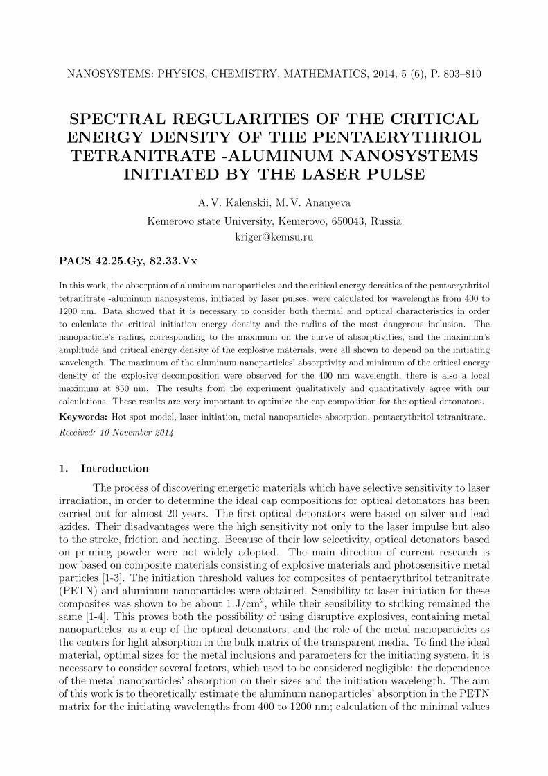
NANOSYSTEMS: PHYSICS, CHEMISTRY, MATHEMATICS, 2014, 5 (6), P. 803–810
SPECTRAL REGULARITIES OF THE CRITICALENERGY DENSITY OF THE PENTAERYTHRIOLTETRANITRATE -ALUMINUM NANOSYSTEMS
INITIATED BY THE LASER PULSE
A. V. Kalenskii, M. V. Ananyeva
Kemerovo state University, Kemerovo, 650043, Russia
PACS 42.25.Gy, 82.33.Vx
In this work, the absorption of aluminum nanoparticles and the critical energy densities of the pentaerythritol
tetranitrate -aluminum nanosystems, initiated by laser pulses, were calculated for wavelengths from 400 to
1200 nm. Data showed that it is necessary to consider both thermal and optical characteristics in order
to calculate the critical initiation energy density and the radius of the most dangerous inclusion. The
nanoparticle’s radius, corresponding to the maximum on the curve of absorptivities, and the maximum’s
amplitude and critical energy density of the explosive materials, were all shown to depend on the initiating
wavelength. The maximum of the aluminum nanoparticles’ absorptivity and minimum of the critical energy
density of the explosive decomposition were observed for the 400 nm wavelength, there is also a local
maximum at 850 nm. The results from the experiment qualitatively and quantitatively agree with our
calculations. These results are very important to optimize the cap composition for the optical detonators.
Keywords: Hot spot model, laser initiation, metal nanoparticles absorption, pentaerythritol tetranitrate.
Received: 10 November 2014
1. Introduction
The process of discovering energetic materials which have selective sensitivity to laserirradiation, in order to determine the ideal cap compositions for optical detonators has beencarried out for almost 20 years. The first optical detonators were based on silver and leadazides. Their disadvantages were the high sensitivity not only to the laser impulse but alsoto the stroke, friction and heating. Because of their low selectivity, optical detonators basedon priming powder were not widely adopted. The main direction of current research isnow based on composite materials consisting of explosive materials and photosensitive metalparticles [1-3]. The initiation threshold values for composites of pentaerythritol tetranitrate(PETN) and aluminum nanoparticles were obtained. Sensibility to laser initiation for thesecomposites was shown to be about 1 J/cm2, while their sensibility to striking remained thesame [1-4]. This proves both the possibility of using disruptive explosives, containing metalnanoparticles, as a cup of the optical detonators, and the role of the metal nanoparticles asthe centers for light absorption in the bulk matrix of the transparent media. To find the idealmaterial, optimal sizes for the metal inclusions and parameters for the initiating system, it isnecessary to consider several factors, which used to be considered negligible: the dependenceof the metal nanoparticles’ absorption on their sizes and the initiation wavelength. The aimof this work is to theoretically estimate the aluminum nanoparticles’ absorption in the PETNmatrix for the initiating wavelengths from 400 to 1200 nm; calculation of the minimal values
804 A.V. Kalenskii, M.V. Ananyeva
of the critical energy density for PETN – aluminum composites for different inclusion sizesand initiating wavelengths.
2. Hot spot model
The hot spot model [1-4] is based on the assumption that in the matrix of the en-ergetic material there are nanoparticles, which can absorb irradiation very efficiently. Inthis model, it is assumed that the main result of light absorption is the heating of theseparticles. The heating causes growth of the surrounding energetic material’s temperatureand formation of the center of the self-accelerating exothermic reaction. The system of equa-tions, describing conductive heat-transfer processes in the nanoparticles and media and theexothermal decomposition in case of the spherical symmetry, are [2-5]:
∂T
∂t= α ·
(∂2T
∂x2+
2
x· ∂T∂x
)+Q
ck0n · exp
(− E
kBT
), x > R,
∂n
∂t= −k0n · exp
(− E
kBT
), x > R, (1)
∂T
∂t= αM ·
(∂2T
∂x2+
2
x· ∂T∂x
), x < R,
where T – temperature, n – relative concentration of the explosive material (PETN), whichdecreases during the reaction from 1 to 0, α and αM – are the coefficients of thermal con-ductivity of the matrix and inclusion materials, R is the inclusion radius, kB – Boltzmannconstant, E – energy of activation, Q – heat efficiency of the decomposition, k 0 – preexpo-nential factor, c is the volumetric heat capacity of the matrix. The boundary conditions forx = R are:
J − cMαM ·∂T
∂x
∣∣∣∣x→R−0
+ cα · ∂T∂x
∣∣∣∣x→R+0
= 0, (2)
where cM is the volumetric heat capacity of the nanoparticle, J(t) – is the absorbed densityof the laser pulse radiation power. During the calculations the following parameters wereused (the same as in works [2-5]): = 2.22 J/(cm3K), cM= 2.7 J/(cm3K), = 165 kJ/(mole·K),k0= 1.21016 s−1, α=1.1·10−3 cm2s−1, αM= 0.97 cm2s−1, Q = 9.64 kJ/cm3.
To research the explosive decomposition of energetic materials, the Nd:Yag basedlaser system is often used [6-7]. The dependence of the laser’s radiating power on time isclose to the function of the normal distribution [7-8]. Taking as a zero-time the moment ofthe impulse’s maximum, one can obtain for J(t) the following equation [9-10]:
J(t) =√π ·QabsR
2kiH0 · exp(−k2i t2
), (3)
where ki = 8.325·107 c−1 – parameter, determining the impulse duration (corresponds to theimpulse duration on the half-height 20 ns); H0 – impulse energy density; Qabs – the coefficientof absorption efficiency equal to the ratio of intensities of radiation absorbed and incidenton the inclusion. The value of Qabs depends on different factors – the inclusion radius andmaterial of inclusion, and radiation wavelength. Multipliers of Eq. (3) normalize the integralof J(t) over time by H0.
Qabs of the spherical inclusion was calculated in terms of Mie theory. According tothis theory, Qabs might be calculated as a difference between coefficients of extinction (Q)
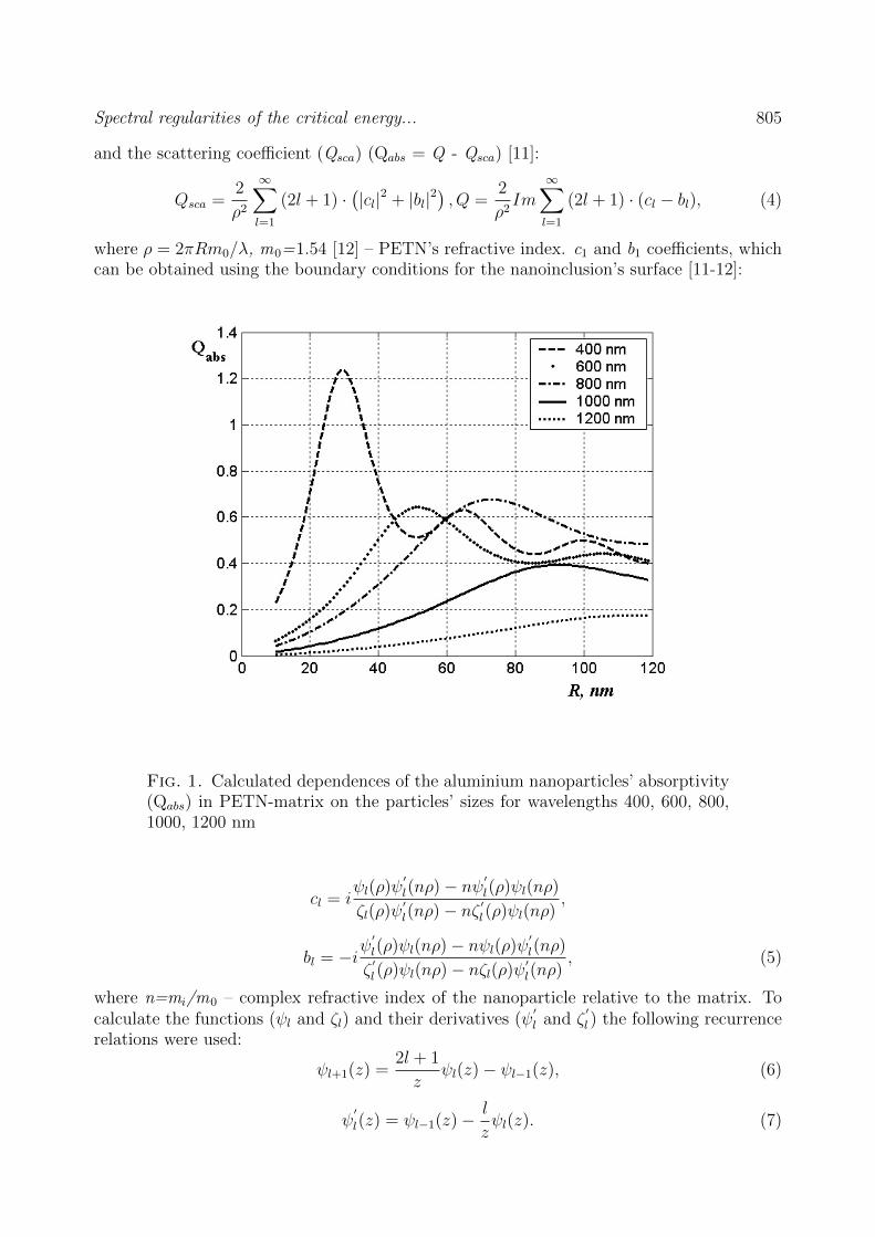
Spectral regularities of the critical energy... 805
and the scattering coefficient (Qsca) (Qabs = Q - Qsca) [11]:
Qsca =2
ρ2
∞∑l=1
(2l + 1) ·(|cl|2 + |bl|2
), Q =
2
ρ2Im
∞∑l=1
(2l + 1) · (cl − bl), (4)
where ρ = 2πRm0/λ, m0=1.54 [12] – PETN’s refractive index. c1 and b1 coefficients, whichcan be obtained using the boundary conditions for the nanoinclusion’s surface [11-12]:
Fig. 1. Calculated dependences of the aluminium nanoparticles’ absorptivity(Qabs) in PETN-matrix on the particles’ sizes for wavelengths 400, 600, 800,1000, 1200 nm
cl = iψl(ρ)ψ
′
l(nρ)− nψ′
l(ρ)ψl(nρ)
ζl(ρ)ψ′l(nρ)− nζ ′
l (ρ)ψl(nρ),
bl = −iψ′
l(ρ)ψl(nρ)− nψl(ρ)ψ′
l(nρ)
ζ′l (ρ)ψl(nρ)− nζl(ρ)ψ
′l(nρ)
, (5)
where n=mi/m0 – complex refractive index of the nanoparticle relative to the matrix. Tocalculate the functions (ψl and ζl) and their derivatives (ψ
′
l and ζ′
l ) the following recurrencerelations were used:
ψl+1(z) =2l + 1
zψl(z)− ψl−1(z), (6)
ψ′
l(z) = ψl−1(z)− l
zψl(z). (7)
806 A.V. Kalenskii, M.V. Ananyeva
If l = 1; 2 the special functions are:
ψ0(z) = sin z ψ1(z) =sin z
z− cos z, (8)
ζ0(z) = ie−iz ζ1(z) = −e−iz(1− i/z). (9)
The use of recurrence relations (6-9) greatly shortened the time required for calcu-lation. Dependences of the aluminum nanoparticles’ absorptivity in the PETN-matrix onthe particles’ sizes, calculated using equation (4-9) are presented in fig. 1. Calculationswere done for different initiating wavelengths – 400, 600, 800, 1000, and 1200 nm. Eachdependence has a maximum (Qabs max), its position (Rmax) depending on the irradiationwavelength. For smaller radii, the curve decreases to zero, and in the extreme case R→0,the dependence changes according to Rayleigh–Jeans law. For nanoparticles having largerradii, the curve plateaus with some oscillations. In terms of the Mie theory, the wavelengthinfluences the Qabs because the factorial expansion arguments of the special functions areρ = 2πRm0/λ and miρ/m0. If mi did not depend on the wavelength, the Qabs(ρ) depen-dences would coincide. The real and imaginary parts of mi change considerably over therange of the examined wavelengths (Table 1). Table 1 shows the following: complex refrac-tive index of aluminum [13], the calculated radii of aluminum particles having the largestabsorptivity and those absorptivity values. The results presented for the wavelengths from400 to 1200 nm, for which the complex refractive index of aluminum are well known [13-14],and for wavelengths of 1064 and 532 nm – the first and the second harmonic of the Nd:YAGlaser using in the experimental work [2-3]. If the wavelength increases, the absorptivity max-imum moves to the area of the larger radii (fig. 1), the maximum’s amplitude – decreases(fig. 2). But for λ =850 nm there is a local maximum, caused by the local maxima of the realand imaginary parts of the complex refractive index. Thus, for the Qabs max(λ) dependencefor aluminum in a PETN-matrix, there is a local maximum, and so, there must be corre-sponding minimum of critical initiation energy for explosive decomposition. The calculatedQabs max(λ) dependence over wavelengths ranging from 400–1200 nm is presented on fig. 2.
In order to calculate the critical parameters for explosive decomposition, a numericalsolution for models (1)–(3) was made using a variable-pitch grid. A step in the vicinity ofthe inclusions with the radii R>30 nm was no more than 1/20 of the thickness of the inert
substance heated during the pulse (√
2α/ki), then the cell size increased exponentially, sothat the total thickness of the surrounding material was no less than 7R. For a half-heightpulse duration of 20 ns, the heating length was equal to ≈50 nm and the size of cells nearthe inclusion was about 2.5 nm. The step of the grid inside the inclusion exceeded thestep outside by
√αM/α times. The cell on the bound inclusion-matrix contained both the
matrix material and the inclusion material with the thickness equal to the half step of thegrid. For the mentioned characteristics, the size of the cell inside the inclusion was about10 nm, which is approximately the thickness of the light absorption layer. This layer does notexceed 10 nm for most metals. This method allows one to make a reasonable considerationof light absorption by means of boundary conditions (2) [15].
The ordinary differential equation set obtained after dividing the space into cells wassolved by the Runge — Kutta method of 1–5 orders with a variable time step. A relative errorat an integration step does not exceed 10−9, whereas the integral relative error estimated bythe precision of performance of the law of conservation of energy did not exceed 2.5·10−5.
Calculation of the radius of the most dangerous inclusion was made using the followingmethod. First the absorptivities for the different particles’ radii were calculated. Then, thecritical energy density was calculated for these radii in terms of models (1-3). Next, quadratic
Spectral regularities of the critical energy... 807
Fig. 2. Dependences of the aluminum nanoparticles’ maximal absorptivity inPETN matrix on the initiating wavelength in a spectral range 400 – 1200 nm
interpolation was done to obtain the minimal value results. After that, the critical energydensity was calculated at the point of this minimum. All these steps were repeated until themost dangerous inclusion’s radius accuracy became 0.1 nm.
Fig. 3 shows dependences of the critical energy density on the radius of the aluminuminclusion in the PETN-matrix for initiating wavelengths of 532, 700, 850, 900, and 1064 nm.For each wavelength, there is an optimum radius of the nanoparticle (Rc), which correspondsto the minimum critical energy density (Hc), for the definite impulse duration. Values Rc
and Rmax for each wavelength have some differences (see table), this is due to the particu-larities of the nanoparticle heating by the laser pulse in solid-state matrix. For 20 ns pulseduration, there is a size of the nanoparticles, which is heated to the maximum temperature(particularities of the absorption were not considered – Qabs = 1). The absorption crosssection of the particle is πR2, heat capacity of the system nanoparticle – matrix layer might
be written as 4π3·(cMR
3 + c
((R +
√2α/ki
)3−R3
))[11], where h ≈
√2α/ki – thickness
of the energetic material’s layer, which is heated during the laser action. Therefore, thedependence of the heat rate (∆T) of the particle on the nanoparticle’s sizes during the pulseaction is:
∆T =HR/4c
Rξ1√
2α/ki + ξ21 · 2α/ki + cMR2/3c, (10)
where ξ1 – variable parameter, its value is about 1 [11].
808 A.V. Kalenskii, M.V. Ananyeva
Table 1. Calculated parameters for the absorption and explosive decompo-sition process of the aluminum-PETN composites – complex refractive index(mi), maximum of absorptivity (Qabs max) and particle’s radius Rmax corre-sponding to this maximum, minimum of critical energy density (Hc), optimalparticle’s radius Rc
λ,nm
mi Qabs max Rmax,nm
Hc, µJ/cm2 Rc, nm
400 0.32-3.72i 1.2358 30 7.25 30.7
450 0.41-4.06i 1.0410 35 7.93 36.1
500 0.5-4.59i 0.7815 41 9.93 42.1
532 0.56-4.86i 0.7064 44 10.66 45.8
550 0.6-5.01i 0.6799 46 10.93 47.6
600 0.77-5.46i 0.6419 52 11.25 53.1
650 0.98-5.97i 0.6090 57 11.59 58.6
700 1.26-6.4i 0.6210 63 11.22 63.8
750 1.5-6.72i 0.6307 68 10.95 68.8
800 1.78-6.87i 0.6771 73 10.16 73.5
850 1.91-6.9i 0.7027 78 9.77 77.7
875 1.82-6.87i 0.6871 80 9.99 79.7
900 1.7-6.97i 0.6364 82 10.79 81.8
950 1.4-7.22i 0.51 87 13.52 86.6
1000 1.17-7.58i 0.3939 93 17.58 92.1
1064 0.98-8.03i 0.2942 100 23.66 98.7
1100 0.85-8.33i 0.2375 104 29.43 102.2
1200 0.78-9.16i 0.1757 115 40.48 111.6
Maximum of the dependence corresponds to the Rm = ξ1√
3c/cM ·√
2α/ki. Theexistence of the optimal nanoparticle’s size for which the heating rate is maximal was pos-tulated in previous works. If the half-height pulse duration is 20 ns, then Rm=75 nm.Table 1 shows the calculated minimum energy densities for the explosive decomposition ofaluminum-PETN composites, optimal radius with the minimal initiating energy density forthe laser wavelengths from 400 to 1200 nm. If λ 6800 nm, the radius, corresponding to theabsorptivity maximum, Rmax <Rm (75 nm), and so the optimal radius, corresponding tothe minimal critical energy density, Rc >Rmax, i.e. the optimal radius for explosive decom-position initiation is larger than the radius, corresponding to the absorptivity maximum.If λ >850 nm Rmax >Rm, and so the optimal radius of the particle is smaller than theradius, corresponding to the maximum of absorptivity. Calculated critical energy densitiesare minimal if λ = 400 nm and have local minimum at λ = 850 nm. Minimal critical energydensities for the first harmonic of the Nd:YAG laser in 2.2 times bigger than the same valuesfor the second harmonic. This fact is in good agreement with the experimental data (for thefirst harmonic – 1.15 J/cm2, for the second – 0.7 J/cm2 [3]), where this difference is 1.6.

Spectral regularities of the critical energy... 809
Fig. 3. Dependences of the critical energy density on the aluminum nanopar-ticle’s radius in PETN matrix for the initiating wavelengths 532, 700, 850, 900and 1064 nm
3. Conclusion
In this work, the dependences of the absorption of the aluminum nanoparticles andthe critical energy densities of the pentaerythritol tetranitrate-aluminum composites werecalculated for the wavelengths from 400 nm to 1200 nm. It was shown that it is necessary toconsider both thermal and optical characteristics in order to calculate the critical initiationenergy density and the radius of the most dangerous inclusion. The nanoparticle’s radius,corresponding to the maximum on the curve of absorptivities, the maximum’s amplitudeand critical energy density of the explosive materials, were all shown to be dependent uponthe initiating wavelength. The maximum of the aluminum nanoparticles’ absorptivity andminimum of its critical energy density of the explosive decomposition are observed for the400 nm wavelength, there is also a local maximum at the 850 nm wavelength. The results ofthe experiment qualitatively and quantitatively agree with our calculations. These resultsare necessary to determine the ideal cap composition for optical detonators.
Acknowledgments
This work was supported by Ministry of Education and Science of the Russian Fed-eration (governmental project No. 2014/64) and Russian Foundation for Basic Research forthe financial support (grant 14-03-00534 ).

810 A.V. Kalenskii, M.V. Ananyeva
References
[1] Chumakov Yu.A., Knyazeva A.G. Initiation of reaction in the vicinity of a single particle heated by mi-crowave radiation. Fizika goreniya i vzryva, 48(2), P. 24–30 (2012).
[2] Ananyeva M.V., Zvekov A.A., et al. Promising compounds for the cap of optical detonator. Perspektivnyematerialy, 7, P. 5–12 (2014).
[3] Aduev B.P., Nurmukhametov D.R., et al. Vzryvchatoye razlozheniye TENa s nanodobavkami alyu-miniya pri vozdeystvii impulsnogo lazernogo izlucheniya razlichnoy dliny volny. Khimicheskaya fizika,32(8), P. 39–42 (2013).
[4] Kalenskii A.V., Zvekov A.A., et al. Influence of the laser irradiation wavelength on the energetic mate-rials’ initiation critical energy. Fizika goreniya i vzryva, 50(3), P. 98–104 (2014).
[5] Kalenskii A.V., Ananyeva M.V., Zvekov A.A., Zykov I.Yu. Spectrum dependence of the critical energydensity of composites based on pentaerythritol tetranitrate with nikel nanoparticles. Fundamental’nyeproblemy sovremennogo materialovedenia, 11(3), P. 340–345 (2014).
[6] Kriger V.G., Kalenskii A.V., et al. Opredelenie shiriny fronta volny reakcii vzryvnogo razlozhenija azidaserebra. Fizika goreniya i vzryva, 48(4), P. 129–136 (2012).
[7] Korepanov V.I., Lisicyn V.M., Oleshko V.I., Cipilev V.P. K voprosu o kinetike i mehanizme vzryvnogorazlozhenija azidov tjazhelyh metallov. Fizika goreniya i vzryva, 42(1), P. 106–119 (2006).
[8] Aduev B.P., Nurmuhametov D.R., Cipilev V.P., Furega R.I. Vlijanie dobavok ul”tradispersnyh chastical-c na chuvstvitel”nost” tjena k lazernomu vozdejstviju. Fizika goreniya i vzryva, 49(2), P. 102–105(2013).
[9] Kriger V.G., Kalenskii A.V., Ananyeva M.V., Borovikova A.P. Critical initiation-energy density as afunction of single-crystal size in explosive decomposition of silver azide. Fizika goreniya i vzryva, 44(2),P. 76–78 (2008).
[10] Aduev B.P., Ananyeva M.V., et al. Mikroochagovaja model’ lazernogo iniciirovanija vzryvnogo ra-zlozhenija jenergeticheskih materialov s uchetom plavlenija. Fizika goreniya i vzryva, 50(6), P. 92–99(2014).
[11] Kriger V.G., Kalenskii A.V., et al. Vliyaniye effektivnosti pogloshcheniya lazernogo izlucheniya natemperaturu razogreva vklyucheniya v prozrachnykh sredakh. Fizika goreniya i vzryva, 48(6), P. 54–58(2012).
[12] Nikitin A.P. Raschet kriticheskih parametrov iniciirovanija teplovogo vzryva tjena s nanochasticamimedi na raznyh dlinah voln. Mezhdunarodnoe nauchnoe izdanie Sovremennye fundamental’nye i prik-ladnye issledovanija, 4(11), P. 68–75 (2013).
[13] Zolotarev V.M., Morozov V.N., Smirnova E.V. Opticheskie postojannye prirodnyh i tehnicheskih sred.L.: Himija, 216 p. (1984).
[14] Aduev B.P., Nurmukhametov D.R., et al. Integrating Sphere Study of the Optical Properties ofAluminum Nanoparticles in Tetranitropentaerytrite. Zhurnal Tekhnicheskoi Fiziki, 84(9), P. 126–131(2014).
[15] Kriger V.G., Kalenskii A.V., Zvekov A.A., Zykov I.Yu., Nikitin A.P. Protsessy teploperenosa pri lazer-nom razogreve vklyucheny v inertnoy matritse. Teplofizika i aeromekhanika, 20(3), P. 375–382 (2013).
[16] Aleksandrov E. I., Cipilev V. P. Issledovanie vlijanija dlitel’nosti vozbuzhdajushhego impul’sa na chu-vstvitel’nost’ azida svinca k dejstviju lazernogo izluchenija. Fizika goreniya i vzryva, 20(6), P. 104–108(1984).
[17] Burkina R.S., Morozova E.Ju., Cipilev V.P. Iniciirovanie reakcionno-sposobnogo veshhestva potokomizluchenija pri pogloshhenii ego neodnorodnostjami veshhestva. Fizika goreniya i vzryva, 47(5), P. 95–105 (2011).

NANOSYSTEMS: PHYSICS, CHEMISTRY, MATHEMATICS, 2014, 5 (6), P. 811–819
MEASURING LOCAL QUANTUM YIELDOF PHOTOLUMINESCENCE
AND PHOTOTRANSFORMATIONSWITH LASER SCANNING MICROSCOPE
V. V. Zakharov1,2, M. A. Baranov1, A. S. Zlatov1, A. V. Veniaminov1
1ITMO University, St. Petersburg, Russia2Optec LLC, St. Petersburg, Russia
[email protected], [email protected], [email protected],[email protected]
PACS 78.55.Qr, 82.50.-m, 68.37.-d, 82.30.Qt
Measurement of local quantum yields for the photoluminescence of semiconductor nanocrystals (quantum dots)
and photoinduced transformations of dye molecules in polymer films is demonstrated using a laser scanning
microscope capable of mapping luminescence spectra and intensities of transmitted laser light. The confocal
scanning microscope (Zeiss LSM710) was applied for both the induction of photochemical transformations and
measurement The luminescence quantum yield values for quantum dots in different locations of a polymer film
were found to differ, ostensibly depending on their aggregation. To measure photoisomerization quantum yield,
the effects of scanning a tiny area of a polymer film with a focused beam on the intensities of luminescence and
transmitted light were monitored.
Keywords: Confocal microscopy, luminescence, photoisomerization, quantum dot, thioindigo.
Received: 24 November 2014
Revised: 29 November 2014
1. Introduction
Quantum yield (QY) is one of the most important characteristics of photoinduced pro-cesses such as photoluminescence and photochemical transformations. The quantum yield de-pends on intrinsic properties of molecules, nanocrystals, and other species as well as on theirinteractions with the environment. As a rule, only values for QY averaged over relatively largeareas can be measured, while information about their microscopic local values remains hidden.
Nanocomposites with luminescent semiconductor nanocrystals (quantum dots, QD) arewidely used in different areas, such as microelectronics, solar energy conversion, biology andmedicine [1, 2] due to their unusual optical, electrical and structural properties [3]. Spatialheterogeneity of properties is a common feature of nanocomposite materials. Aggregation ofnanoparticles may lead to considerable inhomogeneity of light intensity, decrease of lumines-cence caused by nonradiative energy transfer. The distribution of the QY could be regarded asa quantitative measure of nanocrystal and molecular interactions and provide information aboutefficiency of nanocrystal incorporation in the polymeric matrix. Bulk polymers are known tobe spatially inhomogeneous, and luminescent dyes dissolved in them may serve efficient probesfor testing microheterogeneous environment, provided local QY becomes available.
There are two different approaches to measuring QY of luminescence: (i) direct, orabsolute, which typically requires a spectrophotometer with an integrating sphere, and (ii)comparative, based on relative measurements of light emitted by a specimen under study and
812 V. V. Zakharov, M. A. Baranov, A. S. Zlatov, A. V. Veniaminov
a fluorescent standard with known QY. Traditional techniques of QY measurements, as wellas possible sources of errors, have been analyzed and described in detail [4–9]. In a similarway, the QY of photochemical reactions can be obtained from spectroscopic monitoring ofphotoreaction progress and comparison with phototransformations of etalon substances whoseQY are well established (chemical actinometers) [10] or by direct measurement of exposure.
Various techniques intended for the measurement of absolute luminescence and photore-action QY are known, such as that using a spectrophotometer with integrating sphere [11] orthe dual-beam thermal lens technique [12], but only in a few publications local characteristicswith microscopic resolution have been revealed. Thus, a combined map of topography andsingle-particle fluorescence QY of single particles was obtained using correlated atomic-forceand single-particle fluorescence microscopy [13], however such a technique could hardly beapplied to investigate the inhomogeneous bulk of thick samples.
The present work is aimed at the development of a technique utilizing a confocal laserscanning microscope (LSM) for the measurement of local QY of exemplary photoprocessesinduced by laser light in doped polymer films: quantum dot luminescence and phototransforma-tions of organic molecules such as trans-cis photoisomerization of a thioindigo derivative andphotoreduction of phenanthrenequinone.
2. Experimental
2.1. Instrumentation and calibration
In this study, a Zeiss LSM710 scanning microscope based on Axio Imager Z1 stand, CarlZeiss Microimaging GmbH, Germany, was used to measure QY. Confocal scanning microscopyallows one to obtain digital images with high spatial resolution due to the filtering-out of lightscattered and emitted by out-of-focus optical slices. The LSM is capable of measuring theintensity of laser light transmitted by specimens and obtaining local luminescence spectra.
Prior to applying the microscope for numerical measurements of QY, we needed to assessthe accuracy of light transmittance measured with its help and calibrate the spectral response ofthe microscope photodetector system, in order to ensure correct calculation of photons absorbedby the species and inducing their luminescence or phototransformations.
To verify the accuracy of quantitative measurements using LSM, the transmittance oflaser light by several neutral gray light absorbers (glass plates with thin metal coating ofcontrolled thickness) with well defined optical densities was measured. The measured opticaldensities versus their etalon values are presented in Fig. 1 that demonstrates perfect agreementwithin the range of optical densities up to 1 and slight deviation at O.D.=2.4, for the smallaperture (0.2) lens. In the case of large numerical aperture (0.95), a significant deviationfrom linearity shall be taken into account already for O.D.>0.6, which is already far beyondabsorbance values considered acceptable for luminescence measurements.
For the present study, objective lenses were chosen with sufficiently small numericalaperture (predominantly 0.1 to 0.2) that ensured, along with correct transmittance measurements,‘optical slice thickness’ larger than the sample thickness, to avoid possible uncertainties causedby absorption heterogeneity along the optical axis. Axial resolution of luminescence imagesstrongly depends not only on numerical aperture, but also on the diameter of the confocalpinhole (Fig. 2); however, this does not apply to transmittance measurements that do notinvolve the pinhole.
Spectral calibration of LSM photodetector system was performed using an etalon incan-descent lamp verified at S. I. Vavilov Optical institute (St. Petersburg) as black body with color
Measuring local quantum yield of photoluminescence and phototransformations . . . 813
FIG. 1. Optical density of neutral gray etalon absorbers at 543 nm measured withLSM using two different objective lenses (magnification / numerical aperture:10 × /0.2, squares and 50 × /0.95, circles), vs. nominal etalon optical density.The dashed line is the best linear fit for the low aperture dependence; the solidcurve is exponential fit for the large aperture drawn as a guide to the eye
FIG. 2. Optical slice thickness as a function of numerical apertures of the objec-tive lenses, at confocal pinhole diameters 40 (squares) and 200 µm (circles)
temperature T = 2856 K; the spectra of its emission measured with the LSM was used forcorrection of the luminescence spectra.
Diode (405 nm), Ar+ (488 nm) and He–Ne (543 nm) lasers served as light sources forluminescence excitation and the induction of phototransformations. In order to avoid overheatingof specimens by focused laser beams, not more than a few per cent of maximum power wasused in the measurements. Within these limits, no effect of varied power on the results ofmeasurements was revealed.
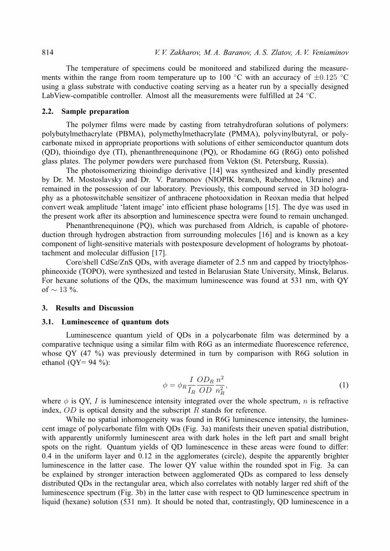
814 V. V. Zakharov, M. A. Baranov, A. S. Zlatov, A. V. Veniaminov
The temperature of specimens could be monitored and stabilized during the measure-ments within the range from room temperature up to 100 C with an accuracy of ±0.125 Cusing a glass substrate with conductive coating serving as a heater run by a specially designedLabView-compatible controller. Almost all the measurements were fulfilled at 24 C.
2.2. Sample preparation
The polymer films were made by casting from tetrahydrofuran solutions of polymers:polybutylmethacrylate (PBMA), polymethylmethacrylate (PMMA), polyvinylbutyral, or poly-carbonate mixed in appropriate proportions with solutions of either semiconductor quantum dots(QD), thioindigo dye (TI), phenanthrenequinone (PQ), or Rhodamine 6G (R6G) onto polishedglass plates. The polymer powders were purchased from Vekton (St. Petersburg, Russia).
The photoisomerizing thioindigo derivative [14] was synthesized and kindly presentedby Dr. M. Mostoslavsky and Dr. V. Paramonov (NIOPIK branch, Rubezhnoe, Ukraine) andremained in the possession of our laboratory. Previously, this compound served in 3D hologra-phy as a photoswitchable sensitizer of anthracene photooxidation in Reoxan media that helpedconvert weak amplitude ‘latent image’ into efficient phase holograms [15]. The dye was used inthe present work after its absorption and luminescence spectra were found to remain unchanged.
Phenanthrenequinone (PQ), which was purchased from Aldrich, is capable of photore-duction through hydrogen abstraction from surrounding molecules [16] and is known as a keycomponent of light-sensitive materials with postexposure development of holograms by photoat-tachment and molecular diffusion [17].
Core/shell CdSe/ZnS QDs, with average diameter of 2.5 nm and capped by trioctylphos-phineoxide (TOPO), were synthesized and tested in Belarusian State University, Minsk, Belarus.For hexane solutions of the QDs, the maximum luminescence was found at 531 nm, with QYof ∼ 13 %.
3. Results and Discussion
3.1. Luminescence of quantum dots
Luminescence quantum yield of QDs in a polycarbonate film was determined by acomparative technique using a similar film with R6G as an intermediate fluorescence reference,whose QY (47 %) was previously determined in turn by comparison with R6G solution inethanol (QY= 94 %):
φ = φRI
IR
ODR
OD
n2
n2R
, (1)
where φ is QY, I is luminescence intensity integrated over the whole spectrum, n is refractiveindex, OD is optical density and the subscript R stands for reference.
While no spatial inhomogeneity was found in R6G luminescence intensity, the lumines-cent image of polycarbonate film with QDs (Fig. 3a) manifests their uneven spatial distribution,with apparently uniformly luminescent area with dark holes in the left part and small brightspots on the right. Quantum yields of QD luminescence in these areas were found to differ:0.4 in the uniform layer and 0.12 in the agglomerates (circle), despite the apparently brighterluminescence in the latter case. The lower QY value within the rounded spot in Fig. 3a canbe explained by stronger interaction between agglomerated QDs as compared to less denselydistributed QDs in the rectangular area, which also correlates with notably larger red shift of theluminescence spectrum (Fig. 3b) in the latter case with respect to QD luminescence spectrum inliquid (hexane) solution (531 nm). It should be noted that, contrastingly, QD luminescence in a
Measuring local quantum yield of photoluminescence and phototransformations . . . 815
polyvinylbutyral film was found to be uniform, with QY = 0.23 and maximum luminescence at534 nm.
FIG. 3. a) Luminescent image of a 80×80 µm part of a polycarbonate film withCdSe/ZnS nanocrystals; excitation wavelength 405 nm; b) luminescence spectraof the film region within the rectangle 1 and the bright spot in the centre ofthe circle 2 (squares and circles, respectively). Solid lines are best Gaussianfits; dotted lines depict the maxima of luminescence intensity at 537 (1) and543 nm (2). Notice the lower intensity in the area 1 with QY larger than that inthe area 2
3.2. Photoisomerization of thioindigo dye
The thioindigo dye exists in two isomeric forms that can undergo reversible phototrans-formations accompanied by dramatic spectral changes. In Fig. 4, absorption spectra of theTI-doped PBMA film obtained after exposures to mercury arc light with wavelengths 578 nm(curve 1) and 436 nm (2) are plotted, representing almost pure trans-isomer and isomer mixturewith predominant contribution of cis-isomer, respectively. Only trans-TI molecules are capableof fluorescence [14, 18] whose intensity can be then a measure of their concentration. Almostidentical fluorescence spectra acquired with LSM and Cary Eclipse spectrofluorimeter are alsopresented in Fig. 4 (3 and 4, respectively).
To study trans-cis-photoisomerization of TI, different exposures of actinic light wereapplied to small strip-shaped areas of the specimen by scanning them with a He-Ne laser(543 nm) of the microscope, followed by monitoring transmittance and luminescence excitedby properly attenuated light of the same laser. The intensities of emitted and transmitted lightare shown in Fig. 5 as functions of exposure. Before the measurements, the dye in the filmwas brought into the trans-isomeric form by uniform exposure to 436 nm light of a 120 Whigh-pressure mercury lamp.
Unlike fluorescence, light absorbance at the excitation wavelength does not exclusivelybelong to trans-isomer. Therefore, the optical density of the film at 543 nm can be taken as ameasure of trans-isomer concentration only at low degree of trans-cis conversion, in the initialstage of the process. Hence, we consider luminescence intensity more reliable for monitoringthe dynamics of phototransformation, while the initial value of optical density was used todetermine the number of TI molecules.
816 V. V. Zakharov, M. A. Baranov, A. S. Zlatov, A. V. Veniaminov
FIG. 4. Absorption spectra of polymer film with thioindigo dye exposed to lightwith wavelength 436 nm (1, dash-dotted line, almost pure trans-isomer) and578 nm (2, dashed line, predominantly cis-isomer with small contribution oftrans-isomer); fluorescence spectra measured with LSM (3, dotted line) and CaryEclipse spectrofluorimeter (4, solid line; excitation at 405 nm)
FIG. 5. Photoisomerization of thioindigo in PBMA film monitored with LSM:intensities of transmitted excitation light (543 nm, solid line, T) and luminescenceof the trans-isomer (dashed line, L) as functions of exposure
Measuring local quantum yield of photoluminescence and phototransformations . . . 817
The QY of the trans-cis photoisomerization can be calculated as ratio of the number∆DNAS/α of molecules within the illuminated area S converted from trans- to cis-isomerdivided by the number E (1 − T ) /hν of absorbed photons with energy hν:
φtc =∆DSNAhν
Eα (1 − T ), (2)
with ∆D- the small photoinduced change of optical density caused by exposure to light energyE, NA – Avogadro number, a = 8700 Lmol−1·cm−1 – molar absorption coefficient of trans-TIcalculated using the spectroscopic data available from [14], T – transmittance of the doped filmat 543 nm.
The initial (measured when almost all the dye was in trans-isomeric form) value ofφtc= 0.006 is between the values previously reported for QY of trans-cis isomerization of TIin more rigid PMMA and in liquid butyl acetate solution, 0.001 and 0.06, respectively [19].During photoisomerization, φtc dramatically decreased after about 30 – 35 % of trans-moleculeshad been converted to the cis-isomer (Fig. 6). This was presumably due to the significantlyheterogeneous distribution of free volume needed for restructuring dye molecules in the bulkpolymer, even though glass transition temperature of PBMA is quite close to the measurementtemperature. Contrastingly, QY of fluorescence that apparently does not require much freevolume did not significantly vary from its initial value (0.15).
FIG. 6. Quantum yields of isomerization (squares, I) and luminescence (cir-cles, L) as functions of degree of dye conversion from trans- to cis-isomericform in the course of isomerization. Lines are guides to the eye
3.3. Photoreduction of phenanthrenequinone
Photoreduction of PQ provided another example of a photochemical process for thisstudy. Different doses of laser light (488 nm) were applied to 50×50 µm squares of PQ-dopedPMMA film using the scanning microscope (Fig. 7a). As a result of the exposure, PQ waspartially bleached and the film transmittance has grown, as well as its luminescence intensity(Fig. 7b) – the situation contrary to that of photoisomerization (cf. Figs. 5 and 8). Thismeans that the luminescence belongs to the photoproduct, despite the latter is known to havealmost negligible absorption in the visible range. Because absorbance of the photoproduct at thewavelength of excitation remained unknown, no QY of its luminescence could be calculated.
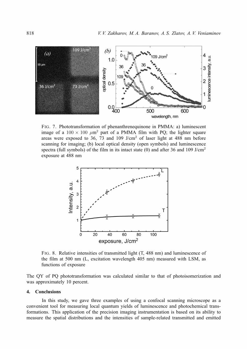
818 V. V. Zakharov, M. A. Baranov, A. S. Zlatov, A. V. Veniaminov
FIG. 7. Phototransformation of phenanthrenequinone in PMMA: a) luminescentimage of a 100 × 100 µm2 part of a PMMA film with PQ; the lighter squareareas were exposed to 36, 73 and 109 J/cm2 of laser light at 488 nm beforescanning for imaging; (b) local optical density (open symbols) and luminescencespectra (full symbols) of the film in its intact state (0) and after 36 and 109 J/cm2
exposure at 488 nm
FIG. 8. Relative intensities of transmitted light (T, 488 nm) and luminescence ofthe film at 500 nm (L, excitation wavelength 405 nm) measured with LSM, asfunctions of exposure
The QY of PQ phototransformation was calculated similar to that of photoisomerization andwas approximately 10 percent.
4. Conclusions
In this study, we gave three examples of using a confocal scanning microscope as aconvenient tool for measuring local quantum yields of luminescence and photochemical trans-formations. This application of the precision imaging instrumentation is based on its ability tomeasure the spatial distributions and the intensities of sample-related transmitted and emitted
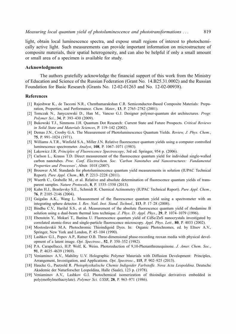
Measuring local quantum yield of photoluminescence and phototransformations . . . 819
light, obtain local luminescence spectra, and expose small regions of interest to photochemi-cally active light. Such measurements can provide important information on microstructure ofcomposite materials, their spatial heterogeneity, and can also be helpful if only a small amountor small area of a specimen is available for study.
Acknowledgments
The authors gratefully acknowledge the financial support of this work from the Ministryof Education and Science of the Russian Federation (Grant No. 14.B25.31.0002) and the RussianFoundation for Basic Research (Grants No. 12-02-01263 and No. 12-02-00938).
References
[1] Rajeshwar K., de Tacconi N.R., Chenthamarakshan C.R. Semiconductor-Based Composite Materials: Prepa-ration, Properties, and Performance. Chem. Mater., 13, P. 2765–2782 (2001).
[2] Tomczak N., Janyczewski D., Han M., Vancso G.J. Designer polymer-quantum dot architectures. Progr.Polymer Sci., 34, P. 393–430 (2009).
[3] Bukowski T.J., Simmons J.H. Quantum Dot Research: Current State and Future Prospects. Critical Reviewsin Solid State and Materials Sciences, P. 119–142 (2002).
[4] Demas J.N., Crosby G.A. The Measurement of Photoluminescence Quantum Yields. Review, J. Phys. Chem.,75, P. 991–1024 (1971).
[5] Williams A.T.R., Winfield S.A., Miller J.N. Relative fluorescence quantum yields using a computer controlledluminescence spectrometer. Analyst, 108, P. 1067–1071 (1983).
[6] Lakowicz J.R. Principles of Fluorescence Spectroscopy, 3rd ed. Springer, 954 p. (2006).[7] Carlson L., Krauss T.D. Direct measurement of the fluorescence quantum yield for individual single-walled
carbon nanotubes. Proc. Conf. Electrochem. Soc. ‘Carbon Nanotubes and Nanostructures: FundamentalProperties and Processes’, Abstr. 1018 (2007).
[8] Brouwer A.M. Standards for photoluminescence quantum yield measurements in solution (IUPAC TechnicalReport). Pure Appl. Chem., 83, P. 2213–2228 (2011).
[9] Wuerth C., Grabolle M., et al. Relative and absolute determination of fluorescence quantum yields of trans-parent samples. Nature Protocols, 8, P. 1535–1550 (2013).
[10] Kuhn H.J., Braslavsky S.E., Schmidt R. Chemical Actinometry (IUPAC Technical Report). Pure Appl. Chem.,76, P. 2105–2146 (2004).
[11] Gaigalas A.K., Wang L. Measurement of the fluorescence quantum yield using a spectrometer with anintegrating sphere detector. J. Res. Natl. Inst. Stand. Technol., 113, P. 17–28 (2008).
[12] Bindhu C.V., Harilal S.S., et al. Measurement of the absolute fluorescence quantum yield of rhodamine Bsolution using a dual-beam thermal lens technique. J. Phys. D: Appl. Phys., 29, P. 1074–1079 (1996).
[13] Ebenstein Y., Mokari T., Banina U. Fluorescence quantum yield of CdSe/ZnS nanocrystals investigated bycorrelated atomic-force and single-particle fluorescence microscopy. Appl. Phys. Lett., 80, P. 4033 (2002).
[14] Mostoslavskii M.A. Photochromic Thioindigoid Dyes. In: Organic Photochromes, ed. by Eltsov A.V.,Springer, New York and London, P. 45–104 (1990).
[15] Lashkov G.I., Popov A.P., Ratner O.B. Three-dimensional phase-recording reoxan media with physical devel-opment of a latent image. Opt. Spectrosc., 52, P. 350–352 (1982).
[16] P.A. Carapellucci, H.P. Wolf, K. Weiss. Photoreduction of 9,10-Phenanthrenequinone. J. Amer. Chem. Soc.,91, P. 4635–4639 (1969).
[17] Veniaminov A.V., Mahilny U.V. Holographic Polymer Materials with Diffusion Development: Principles,Arrangement, Investigation, and Applications. Opt. Spectrosc., 115, P. 902–925 (2013).
[18] Haucke G., Paetzold R. Photophysikalische Chemie Indigoider Farbstoffe. Nova Acta Leopoldina. DeutscheAkademie der Naturforscher Leopoldina, Halle (Saale), 123 p. (1978).
[19] Veniaminov A.V., Lashkov G.I. Photochemical isomerization of thioindigo derivatives embedded inpoly(methylmethacrylate). Polymer Sci. USSR, 28, P. 963–971 (1986).
NANOSYSTEMS: PHYSICS, CHEMISTRY, MATHEMATICS, 2014, 5 (6), P. 820–828
HYDROGEN ADSORPTION PROPERTIESOF METAL-ORGANIC FRAMEWORKSWITHIN THE DENSITY-FUNCTIONALBASED TIGHT-BINDING APPROACH
Bassem Assfour*, Thaer assaad, adnan odeh
Department of Chemistry, Atomic Energy Commission of Syria (AECS),P.O. Box 6091, Damascus, Syrian Arab Republic,Tel.: +963 11 213 2580, Fax: +963 11 611 2289
PACS 87.15.ag
Practical methods for hydrogen storage are still a prime challenge in the realization of an energy economy based on
Hydrogen. Metal organic frameworks (MOFs) are crystalline ultra-porous materials with ability to trap and store
voluminous amounts of gas molecules. MOFs represent an encouraging storage method relying on their enormous
surface area. However, MOFs show reduced hydrogen uptake at room temperature due to low adsorption energy
of hydrogen. To increase the adsorption uptake of MOFs at room temperature, the adsorption energy must be
increased. In this contribution, materials exhibiting higher adsorption energy and enhanced hydrogen adsorption,
namely MIL-53 (Al) and MOF-74, have been investigated using molecular dynamics (MD) simulation. MD
simulations were performed within the density functional based tight binding method (DC-SCC-DFTB). Our results
demonstrate that DC-SCC-DFTB method predicts structural parameters, adsorption sites, adsorption energies and
diffusion factors with a very good accuracy, making this method a very powerful tool to investigate various types
of MOF. Moreover, results show that the adsorption energy can be increased by incorporation of transition metals
in MOF structures.
Keywords: Hydrogen storage, Metal Organic Frameworks, Molecular dynamics, DFTB, adsorption energy.
Received: 29 October 2014
Revised: 10 November 2014
1. Introduction
Hydrogen storage in metal organic framework materials (MOFs) attracts significantattention because these materials have enormous specific surface area, low density and a crys-talline structure that can be tailored and chemically functionalized to maximize the adsorptionuptake. MOFs are constructed from metal oxides interconnected by different organic linkers.Thousands of MOFs have been synthesized (only some of them are stable and porous), cate-gorized and carefully studied over the last decade [1, 2]. Some MOFs showed exceptional gasstorage capacity and selectivity [3–5]. The essential issues for hydrogen adsorption in MOFs areboth the strength of adsorption interaction (adsorption energy), and the number and surface ofadsorption sites. The former determines the operation temperature and pressure, and the latterdetermines the storage capacity. The hydrogen adsorption energies on MOFs are ranging from3 to 5 kJ/mol [6,7]. This small adsorption energy is sufficient for H2 adsorption below 80K, butnot at room temperature because an extremely high pressure is needed to make the adsorptionpossible [8]. To store the hydrogen reversibly at room temperature and moderate pressures, the
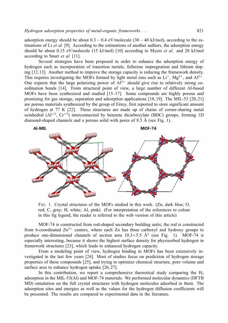
Hydrogen adsorption properties of metal-organic frameworks . . . 821
adsorption energy should be about 0.3 – 0.4 eV/molecule (30 – 40 kJ/mol), according to the es-timations of Li et al. [9]. According to the estimations of another authors, the adsorption energyshould be about 0.15 eV/molecule (15 kJ/mol) [10] according to Myers et al. and 20 kJ/molaccording to Snurr et al. [11].
Several strategies have been proposed in order to enhance the adsorption energy ofhydrogen such as incorporation of transition metals, fullerene impregnation and lithium dop-ing [12,13]. Another method to improve the storage capacity is reducing the framework density.This requires investigating the MOFs formed by light metal ions such as Li+, Mg2+, and Al3+.One expects that the large polarizing power of Al3+ should give rise to relatively strong co-ordination bonds [14]. From structural point of view, a large number of different Al-basedMOFs have been synthesized and studied [15–17]. Some compounds are highly porous andpromising for gas storage, separation and adsorption applications [18, 19]. The MIL-53 [20, 21]are porous materials synthesized by the group of Ferey, first reported to store significant amountof hydrogen at 77 K [22]. These structures are made up of chains of corner-sharing metaloctahedral (Al+3, Cr+3) interconnected by benzene dicarboxylate (BDC) groups, forming 1Ddiamond-shaped channels and a porous solid with pores of 8.5 A (see Fig. 1).
FIG. 1. Crystal structures of the MOFs studied in this work. (Zn, dark blue; O,red; C, gray; H, white; Al, pink). (For interpretation of the references to colourin this fig legend, the reader is referred to the web version of this article)
MOF-74 is constructed from rod-shaped secondary building units; the rod is constructedfrom 6-coordinated Zn2+ centers, where each Zn has three carboxyl and hydroxy groups toproduce one-dimensional channels of section area 10.3×5.5 A2 (see Fig. 1). MOF-74 isespecially interesting, because it shows the highest surface density for physisorbed hydrogen inframework structures [23], which leads to enhanced hydrogen capacity.
From a modeling point of view, hydrogen binding in MOFs has been extensively in-vestigated in the last few years [24]. Most of studies focus on prediction of hydrogen storageproperties of these compounds [25], and trying to optimize chemical structure, pore volume andsurface area to enhance hydrogen uptake [26, 27].
In this contribution, we report a comprehensive theoretical study comparing the H2
adsorption in the MIL-53(Al) and MOF-74 materials. We performed molecular dynamics (DFTBMD) simulation on the full crystal structures with hydrogen molecules adsorbed in them. Theadsorption sites and energies as well as the values for the hydrogen diffusion coefficients willbe presented. The results are compared to experimental data in the literature.
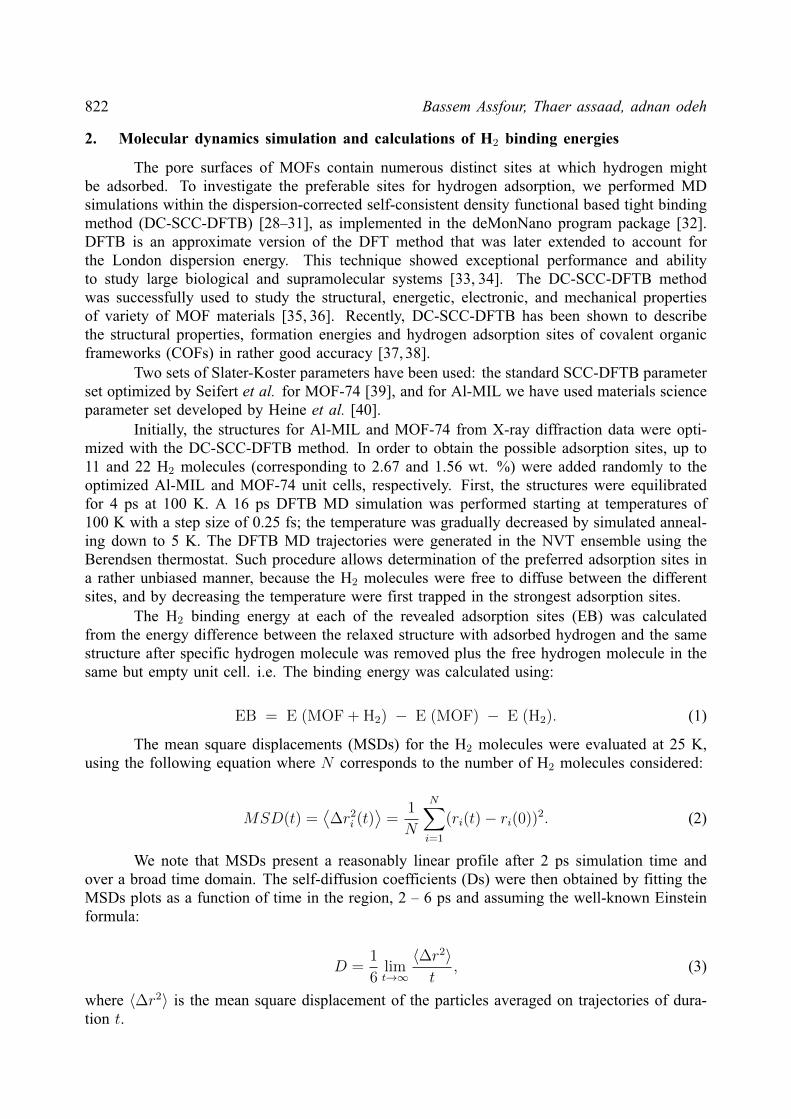
822 Bassem Assfour, Thaer assaad, adnan odeh
2. Molecular dynamics simulation and calculations of H2 binding energies
The pore surfaces of MOFs contain numerous distinct sites at which hydrogen mightbe adsorbed. To investigate the preferable sites for hydrogen adsorption, we performed MDsimulations within the dispersion-corrected self-consistent density functional based tight bindingmethod (DC-SCC-DFTB) [28–31], as implemented in the deMonNano program package [32].DFTB is an approximate version of the DFT method that was later extended to account forthe London dispersion energy. This technique showed exceptional performance and abilityto study large biological and supramolecular systems [33, 34]. The DC-SCC-DFTB methodwas successfully used to study the structural, energetic, electronic, and mechanical propertiesof variety of MOF materials [35, 36]. Recently, DC-SCC-DFTB has been shown to describethe structural properties, formation energies and hydrogen adsorption sites of covalent organicframeworks (COFs) in rather good accuracy [37, 38].
Two sets of Slater-Koster parameters have been used: the standard SCC-DFTB parameterset optimized by Seifert et al. for MOF-74 [39], and for Al-MIL we have used materials scienceparameter set developed by Heine et al. [40].
Initially, the structures for Al-MIL and MOF-74 from X-ray diffraction data were opti-mized with the DC-SCC-DFTB method. In order to obtain the possible adsorption sites, up to11 and 22 H2 molecules (corresponding to 2.67 and 1.56 wt. %) were added randomly to theoptimized Al-MIL and MOF-74 unit cells, respectively. First, the structures were equilibratedfor 4 ps at 100 K. A 16 ps DFTB MD simulation was performed starting at temperatures of100 K with a step size of 0.25 fs; the temperature was gradually decreased by simulated anneal-ing down to 5 K. The DFTB MD trajectories were generated in the NVT ensemble using theBerendsen thermostat. Such procedure allows determination of the preferred adsorption sites ina rather unbiased manner, because the H2 molecules were free to diffuse between the differentsites, and by decreasing the temperature were first trapped in the strongest adsorption sites.
The H2 binding energy at each of the revealed adsorption sites (EB) was calculatedfrom the energy difference between the relaxed structure with adsorbed hydrogen and the samestructure after specific hydrogen molecule was removed plus the free hydrogen molecule in thesame but empty unit cell. i.e. The binding energy was calculated using:
EB = E (MOF + H2) − E (MOF) − E (H2). (1)
The mean square displacements (MSDs) for the H2 molecules were evaluated at 25 K,using the following equation where N corresponds to the number of H2 molecules considered:
MSD(t) =⟨∆r2i (t)
⟩=
1
N
N∑i=1
(ri(t)− ri(0))2. (2)
We note that MSDs present a reasonably linear profile after 2 ps simulation time andover a broad time domain. The self-diffusion coefficients (Ds) were then obtained by fitting theMSDs plots as a function of time in the region, 2 – 6 ps and assuming the well-known Einsteinformula:
D =1
6limt→∞
〈∆r2〉t
, (3)
where 〈∆r2〉 is the mean square displacement of the particles averaged on trajectories of dura-tion t.
Hydrogen adsorption properties of metal-organic frameworks . . . 823
3. Results and discussion
The optimized structure of empty Al-MIL has a shape similar to that reported in theliterature [21], the calculated lattice parameters: (a = 6.76 A, b = 16.91 A, c = 12.59 A)are well comparable with those reported from experiment (a = 6.6085 A, b = 16.6750 A,c = 12.8130 A) at 548 K [21]. The fact that the minimized structure at zero temperature is notexactly the same, but closely related to the experimental one is not surprising in light of thepresence of thermal motion at 548 K.
The results of the DFTB MD simulation at T = 25 K for Al-MIL loaded with molecularhydrogen are shown in Fig. 2. The three sites with the largest adsorption energies are numbered1 – 3 and listed in Table 1. Two of them with the highest adsorption energies (site 1 and 2)are near the AlO6 clusters at the corners of the pore. Site 3 is located over to the benzenering (the organic linker); site 3 has the lowest adsorption energy so it is the least preferredadsorption site for the hydrogen molecules. The average adsorption energy for 11 hydrogenmolecules was found to be 6.35 kJ/mol, and this value was consistent with experimental resultswhere the average heat of adsorption was found to be 5.6 kJ/mol [41]. The maximum totalhydrogen uptake, i.e. when the three adsorption sites are fully occupied, was found to be3.87 wt.%, which compared favorably with 3.8 and 3.1 wt.% measured at 77 K and 16 and 20bar, respectively [22, 41].
FIG. 2. The main three hydrogen adsorption sites in Al-MIL-53 obtained fromDFTB MD simulations. White: hydrogen, dark gray: carbon, red: oxygen, pink:Aluminum. The Hydrogen molecule is plotted in light blue
The optimized structure of empty MOF-74 has a shape similar to that reported in theliterature [23], the optimized (a = 25.987 A, b = 25.981 A, c = 6.846 A) and the experimental(a = b = 25.887 A, c = 6.816 A) lattice parameters are in good agreement. The DFTB MD
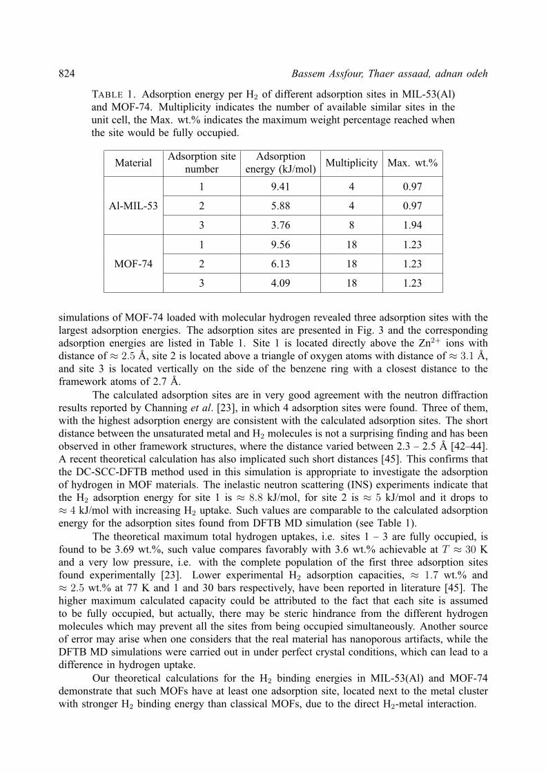
824 Bassem Assfour, Thaer assaad, adnan odeh
TABLE 1. Adsorption energy per H2 of different adsorption sites in MIL-53(Al)and MOF-74. Multiplicity indicates the number of available similar sites in theunit cell, the Max. wt.% indicates the maximum weight percentage reached whenthe site would be fully occupied.
MaterialAdsorption site
numberAdsorption
energy (kJ/mol)Multiplicity Max. wt.%
1 9.41 4 0.97
Al-MIL-53 2 5.88 4 0.97
3 3.76 8 1.94
1 9.56 18 1.23
MOF-74 2 6.13 18 1.23
3 4.09 18 1.23
simulations of MOF-74 loaded with molecular hydrogen revealed three adsorption sites with thelargest adsorption energies. The adsorption sites are presented in Fig. 3 and the correspondingadsorption energies are listed in Table 1. Site 1 is located directly above the Zn2+ ions withdistance of ≈ 2.5 A, site 2 is located above a triangle of oxygen atoms with distance of ≈ 3.1 A,and site 3 is located vertically on the side of the benzene ring with a closest distance to theframework atoms of 2.7 A.
The calculated adsorption sites are in very good agreement with the neutron diffractionresults reported by Channing et al. [23], in which 4 adsorption sites were found. Three of them,with the highest adsorption energy are consistent with the calculated adsorption sites. The shortdistance between the unsaturated metal and H2 molecules is not a surprising finding and has beenobserved in other framework structures, where the distance varied between 2.3 – 2.5 A [42–44].A recent theoretical calculation has also implicated such short distances [45]. This confirms thatthe DC-SCC-DFTB method used in this simulation is appropriate to investigate the adsorptionof hydrogen in MOF materials. The inelastic neutron scattering (INS) experiments indicate thatthe H2 adsorption energy for site 1 is ≈ 8.8 kJ/mol, for site 2 is ≈ 5 kJ/mol and it drops to≈ 4 kJ/mol with increasing H2 uptake. Such values are comparable to the calculated adsorptionenergy for the adsorption sites found from DFTB MD simulation (see Table 1).
The theoretical maximum total hydrogen uptakes, i.e. sites 1 – 3 are fully occupied, isfound to be 3.69 wt.%, such value compares favorably with 3.6 wt.% achievable at T ≈ 30 Kand a very low pressure, i.e. with the complete population of the first three adsorption sitesfound experimentally [23]. Lower experimental H2 adsorption capacities, ≈ 1.7 wt.% and≈ 2.5 wt.% at 77 K and 1 and 30 bars respectively, have been reported in literature [45]. Thehigher maximum calculated capacity could be attributed to the fact that each site is assumedto be fully occupied, but actually, there may be steric hindrance from the different hydrogenmolecules which may prevent all the sites from being occupied simultaneously. Another sourceof error may arise when one considers that the real material has nanoporous artifacts, while theDFTB MD simulations were carried out in under perfect crystal conditions, which can lead to adifference in hydrogen uptake.
Our theoretical calculations for the H2 binding energies in MIL-53(Al) and MOF-74demonstrate that such MOFs have at least one adsorption site, located next to the metal clusterwith stronger H2 binding energy than classical MOFs, due to the direct H2-metal interaction.
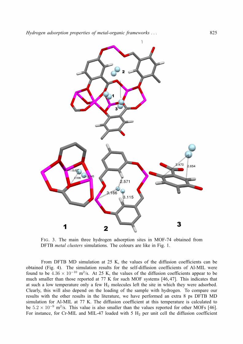
Hydrogen adsorption properties of metal-organic frameworks . . . 825
FIG. 3. The main three hydrogen adsorption sites in MOF-74 obtained fromDFTB metal clusters simulations. The colours are like in Fig. 1.
From DFTB MD simulation at 25 K, the values of the diffusion coefficients can beobtained (Fig. 4). The simulation results for the self-diffusion coefficients of Al-MIL werefound to be 4.36 × 10⁻¹⁰ m2/s. At 25 K, the values of the diffusion coefficients appear to bemuch smaller than those reported at 77 K for such MOF systems [46, 47]. This indicates thatat such a low temperature only a few H2 molecules left the site in which they were adsorbed.Clearly, this will also depend on the loading of the sample with hydrogen. To compare ourresults with the other results in the literature, we have performed an extra 8 ps DFTB MDsimulation for Al-MIL at 77 K. The diffusion coefficient at this temperature is calculated tobe 5.2 × 10⁻⁹ m2/s. This value is also smaller than the values reported for other MOFs [46].For instance, for Cr-MIL and MIL-47 loaded with 5 H2 per unit cell the diffusion coefficient
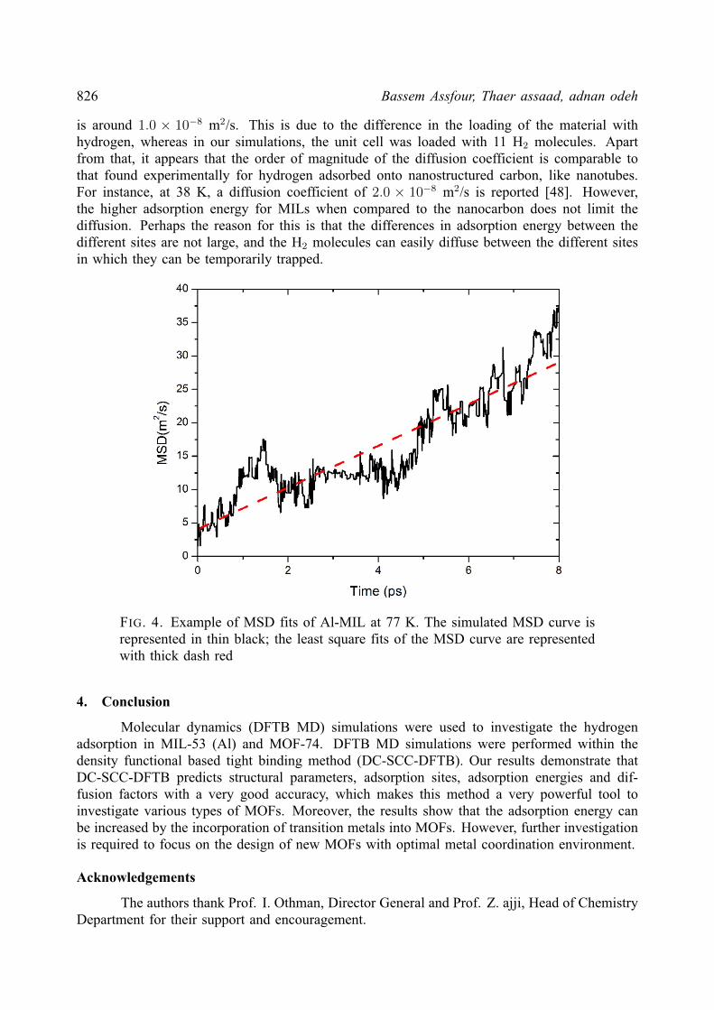
826 Bassem Assfour, Thaer assaad, adnan odeh
is around 1.0 × 10⁻⁸ m2/s. This is due to the difference in the loading of the material withhydrogen, whereas in our simulations, the unit cell was loaded with 11 H2 molecules. Apartfrom that, it appears that the order of magnitude of the diffusion coefficient is comparable tothat found experimentally for hydrogen adsorbed onto nanostructured carbon, like nanotubes.For instance, at 38 K, a diffusion coefficient of 2.0 × 10⁻⁸ m2/s is reported [48]. However,the higher adsorption energy for MILs when compared to the nanocarbon does not limit thediffusion. Perhaps the reason for this is that the differences in adsorption energy between thedifferent sites are not large, and the H2 molecules can easily diffuse between the different sitesin which they can be temporarily trapped.
FIG. 4. Example of MSD fits of Al-MIL at 77 K. The simulated MSD curve isrepresented in thin black; the least square fits of the MSD curve are representedwith thick dash red
4. Conclusion
Molecular dynamics (DFTB MD) simulations were used to investigate the hydrogenadsorption in MIL-53 (Al) and MOF-74. DFTB MD simulations were performed within thedensity functional based tight binding method (DC-SCC-DFTB). Our results demonstrate thatDC-SCC-DFTB predicts structural parameters, adsorption sites, adsorption energies and dif-fusion factors with a very good accuracy, which makes this method a very powerful tool toinvestigate various types of MOFs. Moreover, the results show that the adsorption energy canbe increased by the incorporation of transition metals into MOFs. However, further investigationis required to focus on the design of new MOFs with optimal metal coordination environment.
Acknowledgements
The authors thank Prof. I. Othman, Director General and Prof. Z. ajji, Head of ChemistryDepartment for their support and encouragement.
Hydrogen adsorption properties of metal-organic frameworks . . . 827
References
[1] Furukawa H., Cordova K.E., O’Keeffe M., Yaghi O.M. The Chemistry and Applications of Metal-OrganicFrameworks. Science, 341, 6149 (2013).
[2] Tranchemontagne D.J., Park K.S., et al. Hydrogen Storage in New Metal-Organic Frameworks. The Journalof Physical Chemistry C, 116(24), P. 13143–51 (2012).
[3] Furukawa H., Ko N., et al. Ultrahigh Porosity in Metal-Organic Frameworks. Science, 329 (5990), P. 424-8(2010).
[4] Jiang J. Molecular simulations in metal-organic frameworks for diverse potential applications. MolecularSimulation, 40 (7–9), P. 516–36 (2014).
[5] Keskin S. Gas adsorption and diffusion in a highly CO2 selective metal-organic framework: molecularsimulations. Molecular Simulation, 39 (1), P. 14–24 (2012).
[6] Kuc A., Heine T., Seifert G., Duarte H.A. On the nature of the interaction between H-2 and metal-organicframeworks. Theoretical Chemistry Accounts, 120 (4–6), P. 543–50 (2008).
[7] Dangi G.P., Pillai R.S., et al. A density functional theory study on the interaction of hydrogen molecule withMOF-177. Molecular Simulation, 36 (5), P. 373–81 (2010).
[8] Bae Y-S, Snurr RQ. Molecular simulations of very high pressure hydrogen storage using metal-organicframeworks. Microporous and Mesoporous Materials. 135 (1–3), P. 178–86 (2010).
[9] Li J., Furuta T., et al. Theoretical evaluation of hydrogen storage capacity in pure carbon nanostructures. TheJournal of Chemical Physics, 119 (4), P. 2376–85 (2003).
[10] Bhatia S.K., Myers A.L. Optimum Conditions for Adsorptive Storage. Langmuir, 22 (4), P. 1688–700 (2006).[11] Bae Y.-S., Snurr R.Q. Optimal isosteric heat of adsorption for hydrogen storage and delivery using metal-
organic frameworks. Microporous and Mesoporous Materials, 132 (1–2), P. 300–3 (2010).[12] Thornton A.W., Nairn K.M., et al. Metal-Organic Frameworks Impregnated with Magnesium-Decorated
Fullerenes for Methane and Hydrogen Storage. Journal of the American Chemical Society, 131 (30), P. 10662–9 (2009).
[13] Rao D., Lu R., et al. Influences of lithium doping and fullerene impregnation on hydrogen storage in metalorganic frameworks. Molecular Simulation, 39 (12), P. 968–74 (2013).
[14] Rowsell J.L.C., Yaghi O.M. Strategies for hydrogen storage in metal-organic frameworks. AngewandteChemie-International Edition, 44 (30), P. 4670–9 (2005).
[15] Ahnfeldt T., Guillou N., et al. [Al4(OH)2(OCH3)4(H2N-bdc)3].x H2O: A 12-Connected Porous Metal-OrganicFramework with an Unprecedented Aluminum-Containing Brick. Angewandte Chemie-International Edition,48 (28), P. 5163–6 (2009).
[16] Lin Y., Kong C., Chen L. Facile Synthesis of Aluminum-Based Metal-Organic Frameworks with DifferentMorphologies and Structures through an OH?-Assisted Method. Chemistry - An Asian Journal, 8 (8), P. 1873–8 (2013).
[17] Reinsch H., Kruger M., et al. A new aluminium-based microporous metal-organic framework: Al(BTB)(BTB:1,3,5-benzenetrisbenzoate). Microporous and Mesoporous Materials, 157 (0), P. 50–5 (2012).
[18] Senkovska I., Hoffmann F., et al. New highly porous aluminium based metal-organic frameworks:Al(OH)(ndc) (ndc=2,6-naphthalene dicarboxylate) and Al(OH)(bpdc) (bpdc=4,4 ’-biphenyl dicarboxylate).Microporous and Mesoporous Materials, 122 (1–3), P. 93–8 (2009).
[19] Couck S., Denayer J.F.M., et al. An Amine-Functionalized MIL-53 Metal-Organic Framework with LargeSeparation Power for CO2 and CH4. Journal of the American Chemical Society, 131 (18), P. 6326 (2009).
[20] Serre C., Millange F., et al. Very large breathing effect in the first nanoporous chromium(III)-based solids:MIL-53 or Cr-III(OH).O2C-C6H4-CO2.HO2C-C6H4-CO2Hx. H2Oy . Journal of the American Chemical Soci-ety, 124 (45), P. 13519–26 (2002).
[21] Loiseau T., Serre C., et al. A rationale for the large breathing of the porous aluminum terephthalate (MIL-53)upon hydration. Chemistry - a European Journal, 10 (6), P. 1373–82 (2004).
[22] Ferey G., Latroche M., et al. Hydrogen adsorption in the nanoporous metal-benzenedicarboxylateM(OH)(O2C-C6H4-CO2) (M = Al3+, Cr3+), MIL-53. Chemical Communications, 24, P. 2976–7 (2003).
[23] Liu Y., Kabbour H., et al. Increasing the Density of Adsorbed Hydrogen with Coordinatively UnsaturatedMetal Centers in Metal-Organic Frameworks. Langmuir, 24 (9), P. 4772–7 (2008).
[24] Sculley J., Yuan D., Zhou H.-C. The current status of hydrogen storage in metal-organic frameworks-updated.Energy & Environmental Science, 4 (8), P. 2721–35 (2011).
[25] Goldsmith J., Wong-Foy A.G., Cafarella M.J., Siegel D.J. Theoretical Limits of Hydrogen Storage in Metal-Organic Frameworks: Opportunities and Trade-Offs. Chemistry of Materials, 25 (16), P. 3373–82 (2013).
828 Bassem Assfour, Thaer assaad, adnan odeh
[26] Suraweera N.S., Xiong R., et al. On the relationship between the structure of metal-organic frameworks andthe adsorption and diffusion of hydrogen. Molecular Simulation, 37 (7), P. 621–39 (2011).
[27] Xu Q., Liu D., Yang Q., Zhong C. Molecular simulation study of the quantum effects of hydrogen adsorptionin metal-organic frameworks: influences of pore size and temperature. Molecular Simulation, 35 (9), P. 748–54(2009).
[28] Elstner M.P.D. Jungnickel G., et al. A Self-Consistent Charge Density-Functional Based Tight-Binding Methodfor Predictive Materials Simulations in Physics. Chemistry and Biology physica status solidi (b), 217 (1),P. 41–62 (2000).
[29] Elstner M., Cui Q., et al. Modeling zinc in biomolecules with the self consistent charge-density functional tightbinding (SCC-DFTB) method: Applications to structural and energetic analysis. Journal of ComputationalChemistry, 24 (5), P. 565–81 (2003).
[30] Zhechkov L., Heine T., et al. An efficient a Posteriori treatment for dispersion interaction in density-functional-based tight binding. Journal of Chemical Theory and Computation, 1 (5), P. 841–7 (2005).
[31] Oliveira A.F., Seifert G., Heine T., Duarte H.A. Density-functional based tight-binding: an approximate DFTmethod. Journal of the Brazilian Chemical Society, 20, P. 1193–205 (2009).
[32] Heine T., Rapacioli M., et al. DeMon-nano: Jacobs University Bremen Bremen. Germany (2009).[33] Heine T., Dos Santos H.F., Patchkovskii S., Duarte H.A. Structure and Dynamics of β-Cyclodextrin in
Aqueous Solution at the Density-Functional Tight Binding Level. The Journal of Physical Chemistry A, 111(26), P. 5648–54 (2007).
[34] Zhu X., Koenig P., et al. Establishing effective simulation protocols for β- and α/β-peptides. III. Molecularmechanical model for acyclic β-amino acids. Journal of Computational Chemistry, 31 (10), P. 2063–77(2010).
[35] Kuc A., Enyashin A., Seifert G. Metal-Organic Frameworks: Structural, Energetic, Electronic, and MechanicalProperties. The Journal of Physical Chemistry B, 111 (28), P. 8179–86 (2007).
[36] Lukose B., Supronowicz B., et al. Structural properties of metal-organic frameworks within the density-functional based tight-binding method. Physica status solidi (b), 249 (2), P. 335–42 (2012).
[37] Lukose B., Kuc A., Heine T. The Structure of Layered Covalent-Organic Frameworks. Chemistry - A EuropeanJournal, 17 (8), P. 2388–92 (2011).
[38] Assfour B., Seifert G. Hydrogen adsorption sites and energies in 2D and 3D covalent organic frameworks.Chemical Physics Letters, 489 (1–3), P. 86–91 (2010).
[39] Kuc A., Enyashin A., Seifert G. Metal-organic frameworks: Structural, energetic, electronic, and mechanicalproperties. Journal of Physical Chemistry B, 111 (28), P. 8179–86 (2007).
[40] Frenzel J., Oliveira A.F., et al. Structural and electronic properties of bulk gibbsite and gibbsite surfaces.Zeitschrift Fur Anorganische Und Allgemeine Chemie, 631 (6–7), P. 1267–71 (2005).
[41] Schmitz B., Muller U., et al. Heat of Adsorption for Hydrogen in Microporous High-Surface-Area Materials.Chemphyschem, 9 (15), P. 2181–4 (2008).
[42] Dinca M., Dailly A., et al. Hydrogen Storage in a Microporous Metal-Organic Framework with ExposedMn2+ Coordination Sites. Journal of the American Chemical Society, 128 (51), P. 16876–83 (2006).
[43] Dinc M., Han W.S., et al. Observation of Cu2+–H2 Interactions in a Fully Desolvated Sodalite-Type Metal-Organic Framework. Angewandte Chemie International Edition, 46 (9), P. 1419–22 (2007).
[44] Peterson V.K., Liu Y., Brown C.M., Kepert C.J. Neutron Powder Diffraction Study of D2 Sorption inCu3(1,3,5-benzenetricarboxylate)2. J. Am. Chem. Soc., 128 (49), P. 15578–9 (2006).
[45] Zhou W., Wu H., Yildirim T.. Enhanced H-2 Adsorption in Isostructural Metal-Organic Frameworks withOpen Metal Sites: Strong Dependence of the Binding Strength on Metal Ions. Journal of the AmericanChemical Society, 130 (46), P. 15268-15269 (2008).
[46] Salles F., Kolokolov D.I., et al. Adsorption and Diffusion of H-2 in the MOF Type Systems MIL-47(V)and MIL-53(Cr): A Combination of Microcalorimetry and QENS Experiments with Molecular Simulations.Journal of Physical Chemistry C, 113 (18), P. 7802–12 (2009).
[47] Mulder F.M., Dingemans T.J., Wagemaker M., Kearley G.J. Modelling of hydrogen adsorption in the metalorganic framework MOF5. Chemical Physics, 317 (2–3), P. 113–8 (2005).
[48] Narehood D.G., Pearce J.V., et al. Diffusion of H2 adsorbed on single-walled carbon nanotubes. PhysicalReview B, 67 (20), P. 205409 (2003).
NANOSYSTEMS: PHYSICS, CHEMISTRY, MATHEMATICS, 2014, 5 (6), P. 829–835
NEW ROUTE TO POLY (2,6-DIIMIDAAZO(4,5-b: 4’,5’-e)PYRIDINELENE-1,4(2,5-DIHYDROXY)-PHENYLENE)(PIPD) AND HIGH MODULUS FIBER ON IT BASIS
Jun Li1, Zhen Hu1, Yuanjun Song1, Yudong Huang1∗, V. V. Zuev2,3∗∗
1School of Chemical Engineering and Technology, State Key Laboratory of Urban WaterResource and Environment, Harbin Institute of Technology, 150001 Harbin, China
2ITMO University, Kronverkskiy pr. 49, 197101 Saint Petersburg, Russia3Institute of Macromolecular Compounds of the Russian Academy of Sciences,
Bolshoi pr. 31, 199004 Saint Petersburg, Russia
*[email protected], **[email protected]
PACS 81.07.Lb
A novel entry toward poly( 2,6-diimidazo(4,5-b: 4’,5’-e)pyridinylene-1,4(2,5-dihydroxy)-phenylene) (PIPD) has
been elaborated. A strategy based on a new route to monomers: a sequential nitration of 2,6-diaminopyridine
with KNO3/H2SO4 gives 2,6- diamino- 3,5-dinitro pyridine (DNDAP) in moderate yield and its hydrogenation
with Raney nickel as catalyst leads to 2,3,5,6-tetraaminopyridine (TAP) in high yield. The second monomer
2,5-dihydroxyterephthalate (DHTA) was synthesized in high yield as product of sulfur-mediated aromatization of
dimethyl succinoyl succinate with subsequent base hydrolysis. PIPD was synthesized by step-by-step heating in
polyphosphoric acid with molecular weights of 19 – 25 kilodaltons. The macromolecule of PIPD can be seen as
lap-join chain form nano-sized rigid fragment. The as-polymerized liquid crystalline PIPD solution was used for
fiber spinning. The tensile strength of PIPD fibers were 1.28 – 1.99 GPa and depended on the molecular weight
of the polymer used for spinning.
Keywords: Nano-sized rigid polymer, synthesis, fiber spinning, mechanical properties, liquid crystallinity.
Received: 13 October 2014
Revised: 5 November 2014
1. Introduction
The development of polymer composites over the last 50 years has seen the emergenceof new materials that are lightweight and have exceptional mechanical properties. The com-posite properties depend on filler fiber properties. Traditional inorganic fiber (glass, metal etc)composites deliver exceptional stiffness and stress but can often have a limited extensibility andpoor damage tolerance, especially at low operating temperatures. Unlike carbon and inorganicfibers, rigid-rod polymeric fibers do not show catastrophic failure under compressive stress. Thatfact stimulated researchers to create stiffer rigid-rod-like polymeric materials. The best resultwas been obtained with synthesis of poly (p-phenylene benzobisoxazole) (PBO) [1]. PBO hasvery impressive tensile properties but its performance under compression is disappointing [2].The traditional way to solve this problem in polymer chemistry is cross-linking macromoleculesin the fiber by introducing double bonds into the macromolecule or Υ-irradiation [2]. An al-ternative route to increase the lateral strength of the PBO fiber is introducing intermolecularhydrogen bonds [3]. This choice was realized by the synthesis of poly( 2,6-diimidazo(4,5-b:4’,5’-e)pyridinylene-1,4(2,5-dihydroxy)-phenylene) (PIPD) [4]. This polymer forms in fiber in-termolecular bonds in two dimensions and has the highest compressive strength (1 – 1.7 GPa) of

830 Jun Li, Zhen Hu, Yuanjun Song, Yudong Huang, V.V. Zuev
any polymeric fiber to date [5]. However, the synthetic pathway to this polymer is laborious andexpensive in preparation and purification. The aim of present work is to optimize a procedurefor PIPD synthesis with a view to enhancing of monomer yield, improve the polymerizationto increase the polymer molecular mass, spin a fiber directly from the polymerization solutionwithout polymer precipitation or redissolution by dry-jet wet spinning method, and investigatethe performance of the obtained nano- and macro-sized fibers.
2. Materials and Methods
All used reagents are commercial products were purchased from National medicine Co.Ltd., China, and were used without additional purification. Prior to use, al solvents weredistilled. Hydrogen was purified by passing though columns with a nickel/chromium catalystand molecular sieves.
2.1. Nitration 2,6-diaminopyridine
7 g of KNO3 was mixed with 25 ml of conc. sulfuric acid, and to this was added 3 g of2,6-diaminopyridine. The mixture was stirred at 80 C for 2 h and then at120 C for 1 h. Thereaction mixture was then poured into 500 ml of water and cooled to 5 C. The solution wasneutralized by 20% NaOH, and precipitated 2,6- diamino- 3,5-dinitro pyridine (DNDAP) wascollected after 24 h at 5 C as yellow powder. DNDAP was recrystallized from water-DMSO(7:1 v/v). Yield 4.2 g (76.7). Purity by HPLC 95.8% IR, cm−1: 3473/3359, 1621, 1554,1508,1371, 1322. 1H NMR, (DMSO-d6), δ, ppm : 8.28; 8.44 (2), 9.00 (4). 13C NMR, (DMSO-d6),δ, ppm: 155.21 (ortho), 120.66 (meta), 136.03 (para).
2.2. 2,3,5,6-tetraaminopyridine (TAP)
In a 200 ml autoclave, 10 g of DNDAP, 50 ml of water and 10 ml of 85% phosphoricacid with 1 g of Raney nickel were slurried; the air was displaced with nitrogen and 1.3 kPa ofhydrogen was supplied; the hydrogen pressure was increased to 0.1 MPa and then to 0.5 MPa;the temperature was kept at RT and stirring was continued with the supply of hydrogen at0.5 MPa until the hydrogen consumption ceased (10 h). Without the introduction of air, 20 ml of37% hydrochloric acid was added, and mixture was extruded through the filter from autoclave;to filtrate were added 50 ml of THF and and 25 ml of conc. HCl. The precipitate was filteredoff and dried, yielding 12.9 g TAP·HCl·H2O (93%) with HPLC purity of 99.7%. IR, cm−1:3500 – 2500, 1654, 1610, 1320. 1H NMR, (D2O), δ, ppm : 7.70 (1), 8 – 9 (NH2). 13C NMR,(D2O), δ, ppm: 147.56 (ortho), 102.77 (meta), 131.22 (para).
2.3. Dimethyl 2,5-dihydroxyterephthalate
In a 2 l four-necked flask with stirrer, reflux head, dropping funnel and thermometerwere placed 500 ml of water and 240 ml of glacial acetic acid and in this mixture was dispersed44 g of dimethyl succinyl succinate. The dispersion was heated in a stepwise manner withstirring to 80, 85 and 110 C, and 1 g of each iodine and potassium iodine were added.Without external heating was added 20 ml of 30% hydrogen peroxide in a course of 20 min attemperature 110 C. After ten minutes the 40 ml of warm and than 40 ml of cold water werestirred through reaction mixture. After cooling to RT, the slurry was filtered off and washedtwice with water. After drying, yield 32.7 g (75%), m.p. 153 C.
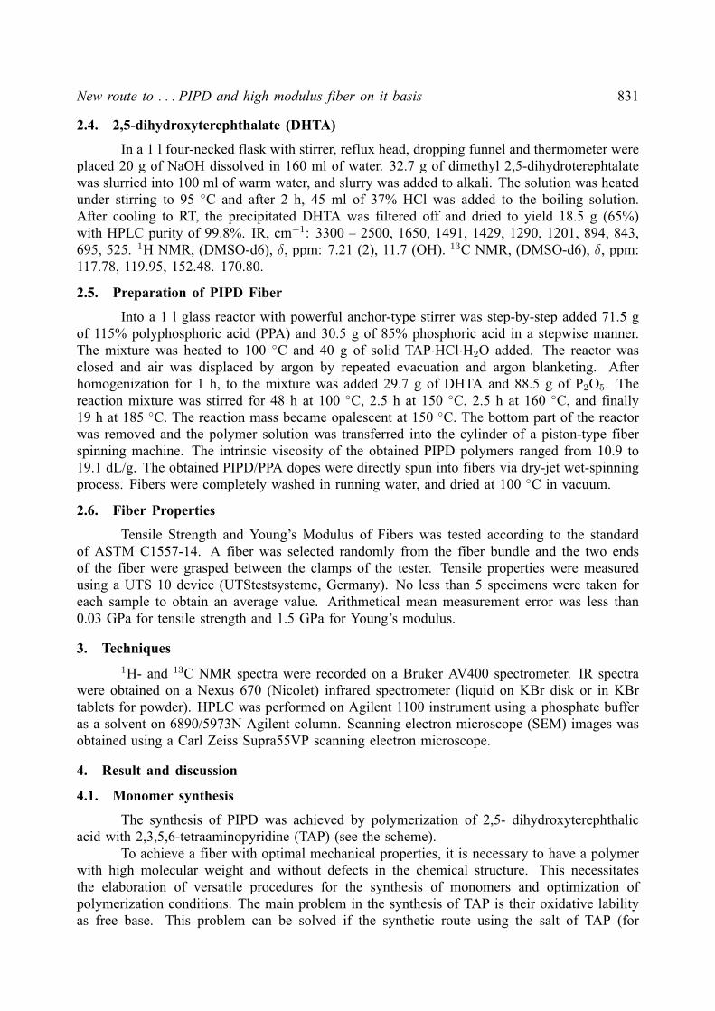
New route to . . . PIPD and high modulus fiber on it basis 831
2.4. 2,5-dihydroxyterephthalate (DHTA)
In a 1 l four-necked flask with stirrer, reflux head, dropping funnel and thermometer wereplaced 20 g of NaOH dissolved in 160 ml of water. 32.7 g of dimethyl 2,5-dihydroterephtalatewas slurried into 100 ml of warm water, and slurry was added to alkali. The solution was heatedunder stirring to 95 C and after 2 h, 45 ml of 37% HCl was added to the boiling solution.After cooling to RT, the precipitated DHTA was filtered off and dried to yield 18.5 g (65%)with HPLC purity of 99.8%. IR, cm−1: 3300 – 2500, 1650, 1491, 1429, 1290, 1201, 894, 843,695, 525. 1H NMR, (DMSO-d6), δ, ppm: 7.21 (2), 11.7 (OH). 13C NMR, (DMSO-d6), δ, ppm:117.78, 119.95, 152.48. 170.80.
2.5. Preparation of PIPD Fiber
Into a 1 l glass reactor with powerful anchor-type stirrer was step-by-step added 71.5 gof 115% polyphosphoric acid (PPA) and 30.5 g of 85% phosphoric acid in a stepwise manner.The mixture was heated to 100 C and 40 g of solid TAP·HCl·H2O added. The reactor wasclosed and air was displaced by argon by repeated evacuation and argon blanketing. Afterhomogenization for 1 h, to the mixture was added 29.7 g of DHTA and 88.5 g of P2O5. Thereaction mixture was stirred for 48 h at 100 C, 2.5 h at 150 C, 2.5 h at 160 C, and finally19 h at 185 C. The reaction mass became opalescent at 150 C. The bottom part of the reactorwas removed and the polymer solution was transferred into the cylinder of a piston-type fiberspinning machine. The intrinsic viscosity of the obtained PIPD polymers ranged from 10.9 to19.1 dL/g. The obtained PIPD/PPA dopes were directly spun into fibers via dry-jet wet-spinningprocess. Fibers were completely washed in running water, and dried at 100 C in vacuum.
2.6. Fiber Properties
Tensile Strength and Young’s Modulus of Fibers was tested according to the standardof ASTM C1557-14. A fiber was selected randomly from the fiber bundle and the two endsof the fiber were grasped between the clamps of the tester. Tensile properties were measuredusing a UTS 10 device (UTStestsysteme, Germany). No less than 5 specimens were taken foreach sample to obtain an average value. Arithmetical mean measurement error was less than0.03 GPa for tensile strength and 1.5 GPa for Young’s modulus.
3. Techniques
1H- and 13C NMR spectra were recorded on a Bruker AV400 spectrometer. IR spectrawere obtained on a Nexus 670 (Nicolet) infrared spectrometer (liquid on KBr disk or in KBrtablets for powder). HPLC was performed on Agilent 1100 instrument using a phosphate bufferas a solvent on 6890/5973N Agilent column. Scanning electron microscope (SEM) images wasobtained using a Carl Zeiss Supra55VP scanning electron microscope.
4. Result and discussion
4.1. Monomer synthesis
The synthesis of PIPD was achieved by polymerization of 2,5- dihydroxyterephthalicacid with 2,3,5,6-tetraaminopyridine (TAP) (see the scheme).
To achieve a fiber with optimal mechanical properties, it is necessary to have a polymerwith high molecular weight and without defects in the chemical structure. This necessitatesthe elaboration of versatile procedures for the synthesis of monomers and optimization ofpolymerization conditions. The main problem in the synthesis of TAP is their oxidative labilityas free base. This problem can be solved if the synthetic route using the salt of TAP (for
832 Jun Li, Zhen Hu, Yuanjun Song, Yudong Huang, V.V. Zuev
example with hydrochloric acid) that avoids any handling of the TAP free base. Such syntheticprocedure was described by Sikkema in [4] and in a number of patents [6–8]. This syntheticpathway included the nitration of commercially-available 2,6-diaminopyridine to 2,6-diamino-3,5-dinitropyridine and its reduction to TAP salt by hydrogenation in solution using differentcatalysts. The best results were obtained using 10 % Pd/C. The yield of final product withpolymer grade purity was about 85% [4]. We used a new route to DNDAP: a sequentialnitration of 2,6-diaminopyridine with KNO3/H2SO4 gives a DNDAP in moderate yield. Wemodified the Sikkema procedure to avoid using a palladium catalyst and replace it by theinexpensive Raney nickel. This allowed us to increase the yield of TAP salt to 93% withan HPLC purity of 99.7%. The second monomer for PIPD synthesis, DHTA, was used inpolymer chemistry, particularly in the synthesis of ‘hairy rod’ liquid crystalline polymers [9].The workable procedure for DHTA synthesis was suggested by Sikkema [4] and was used byus with minor modification. As a result, DHTA was obtained in 65% yield in 99.9% purityas determined by HPLC analysis. Hence, the new synthetic route we developed for PIPDmonomers allowed to obtain both monomers in polymerization-grade purities with high yields.
4.2. Polymerization
For the synthesis PIPD, we used the traditional method with step-by-step heating ofmonomers in weak acid (polyphosphoric acid- PPA). The high-purity monomers allowed us toobtain the polymer (Fig. 1) with high molecular weight (MW) in amounts sufficient for fiberspinning.
For spinning, three samples were selected with MW according capillary viscometry19.1, 22.0 and 25.5 kilodaltons respectively. For calculating the MW, we used the Mark-Kuhn-Houwink equation:
[η] = KMα,
where for K was accepted value 2.27×10⁻⁷ and for α 1.8. The selection constants in the Mark-Kuhn-Houwink equation were based on values recommended for rigid-rod polymers capable offorming H-bonds in solution for viscosity measurements [10]. Capillary viscometry was carriedout in a solution of methanesulfonic acid, which suggests the possibility of a polyelectroliticeffect and as a result, the increase of the calculated values for MW relative to their true value.However, the high tensile strength of spinning fibers supports the high MW of synthesizedPIPD simples. Theoretically calculated values for persistence length was in the range of 22 –65 nm [11–13], which is in good agreement with experimental data for cis-PBO, which wasfound to range from 20 – 30 nm [14] or 50 nm [10]. Hence, the macromolecule of PIPD canbe seen as lap-join chain form nano-sized rigid fragment [11].
The solubility limit of PIPD in the reaction mixture is about 20% for high MW poly-mer. This allowed spinning from the polymerization solution without polymer precipitation andredissolution by dry-jet wet spinning method. It should be noted that solution of PIPD in PPA
New route to . . . PIPD and high modulus fiber on it basis 833
Wavenumbers (cm−1)
FIG. 1. IR spectrum of PIPD
with polymer contain higher than 18 wt% is lyotropic nematic [6] that contribute any specificsin spinning process. Liquid crystallinity offers desirable properties, which make it possible toefficiently spin a thread from such a rigid macromolecule as PIPD.
4.3. Spinning
Conventional air gap wet spinning of the as-polymerized PIPD solution was performedat 180 C in a steam bath for fiber production. As result, filaments with diameter 18 – 20 µm(Fig. 2) were obtained, which were further washed to low phosphorus content and dried toproduce final, high-modulus fibers. In PIPD solutions used for spinning, a high degree ofmolecular orientation of the polymer chains with respect to the local director can be expected.During the spinning process the local directors are aligned in the direction of flow by the shearflow in the capillaries of the spinneret and by the elongation flow in the entrance zone above thespinneret and in the air gap. The high degree of the orientation of the director together with thehigh degree of local molecular order implies that the PIPD macromolecules are highly-oriented.Assuming that this orientation order is merely ‘frozen-in’ during the coagulation process, thehigh modulus of PIPD fiber obtained can be predicted. It was supported by our measurements.The average data for tensile strength of three samples with different MW are 1.28, 1.49 and1.99 GPa. Young’s moduli were 101, 120 and 161 GPa correspondingly. Elongation beforebreak for all samples was about 1%. Hence, this strong dependence of tensile strength on MWshows that polymerization grade of our samples is relative low. However, the absolute value oftensile strength is high compared with literature data [15].
5. Conclusion
A novel entry toward PIPD has been elaborated. A strategy based on a new route tomonomers: a sequential nitration of 2,6-diaminopyridine with KNO3/H2SO4 gives a DNDAPin moderate yield and its hydrogenation with Raney nickel as catalyst leads to TAP in high

834 Jun Li, Zhen Hu, Yuanjun Song, Yudong Huang, V.V. Zuev
FIG. 2. SEM images of PIPD fiber (MW = 25.5 · 103 ) in two directions
yield. Second monomer (DHTA) was synthesized in high yield as product of sulfur-mediatedaromatization of dimethyl succinoyl succinate with following base hydrolysis. PIPD was syn-thesized in a stepwise manner by heating in polyphosphoric acid with MW 19 – 25×103. Themacromolecule of PIPD can be seen as lap-join chain form nano-sized rigid fragment. The as-polymerized liquid crystalline PIPD solution was used for fiber spinning. The tensile strengthof PIPD fibers were 1.28 – 1.99 GPa in dependence on MW polymer used for spinning. PIPDis light as well as strong. Its strength approaches and even exceeds that of typical high strengthengineering steel (1.3 GPa). However, the PIPD have a significantly lower relative density(1.7) [6] than steel (7.8). Compared on a weight basis, PIPD is thus by far the stronger material.
Acknowledgements
The research reported in this paper was partly supported by RFBR-NNSFC grant No. 14-03-91152-a, by National Natural Science Foundation of China (NNSFC) (grant No. 51203034),Research Fund for the Doctoral Program of Higher Education of China (grantNo. 20122302120038), Special Foundation of China Postdoctoral Science (grantNo. 2013T60379), Supported by China Postdoctoral Science Foundation (grantNo. 2013M541392).
References
[1] Norcholt M.G., Sikkema D.J. Lyotropic main chain liquid crystal polymers. Adv. Polym. Sci., 98, P. 115–177(1991).
[2] Sweeny W. Improvements in compressive properties of high modulus fibers by crosslinking. J. Polym. Sci.A, 30, P. 1111–1222 (1992).
[3] Tan L.-S., Arnold F.E., et al. Pseudo-ladder rigid-rod polymers: dihydroxy pendent benzothiazole aromaticheterocyclic polymer and copolymers. Polymer, 35, P. 3091–3101 (1994).
[4] Sikkema D.J. Design, synthesis and properties of a novel rigid rod polymer, PIPD or ‘M5’: high modulusand tenacity fibres with substantial compressive strength. Polymer, 39, P. 5981–5986 (1998).
[5] Klop E.A., Lammers M. XRD study of the new rigid-rod polymer fiber PIPD. Polymer, 39, P. 5987–5998(1998).
[6] Sikkema D.J., Rodini D.J., Adkins, Q.F. High inherent viscosity polymers and fibers therefrom. US patent2006/0280,937 (2006).
New route to . . . PIPD and high modulus fiber on it basis 835
[7] Ritter J. Process for the synthesis PIPD. WIPO patent 2008/066825 (2008).[8] Dindi H., Schultz J.L. Synthesis of dinitrodiaminopyridine. US patent 2012/8115,007 (2012).[9] Balauf M. Rigid-rod polymers having flexible side chain:1. Thermotropic poly(1,4-phenylene 2,5-
dialkoxyterephthalate)s. Macromol. Rapid Commun., 7, P. 407–414 (1986).[10] Roitman D.B., Wessling R.A., McAlister J. Characterization of poly(p-phenylene-cis-benzooxazole) in
methanesulphonic acid. Macromolecules, 26, P. 5174–5184 (1993).[11] Zhang R., Mattice W.L. Evaluation of the persistence length of the rigid-rod polymers poly(benzobisoxazole)
and poly(benzobisthiazole) using molecular-dynamics simulations. Macromolecules, 25, P. 4937–5184 (1992).[12] Zhang R., Mattice W.L. Persistence length of the ‘rodlike’ molecule poly(p-phenylene-trans-benzobisthiazole)
revisited again. Macromolecules, 26, P. 4384–4385 (1993).[13] Roitman D.B., McAdon M. Persistence length of the ‘rodlike’ molecule poly(p-phenylene-trans-
benzobisthiazole) revisited. Macromolecules, 26, P. 4381–4383 (1993).[14] Wong C.-P., Ohnuma H., Berry G.C. Properties of some rodlike polymers in solution. J. Polym. Sci. Polym.
Sym., 65, P. 178–192 (1978).[15] Chae H.G., Kumar S. Rigid rod polymeric fibers. J. Appl. Polym. Sci., 100, P. 791–802 (2006).

NANOSYSTEMS: PHYSICS, CHEMISTRY, MATHEMATICS, 2014, 5 (6), P. 836–842
DIELECTRIC PROPERTIES OF AURIVILLIUSPHASE Bi10Fe6Ti3O30 WITH A NANO-SIZED
PSEUDO-PEROVSKITE BLOCKS
N. A. Lomanova
Ioffe Institute, 26 Polytekhnicheskaya Str., Saint Petersburg 194021, Russia
PACS 61.66.Fn
Distinctive features of dielectric properties of a ceramic material based on Aurivillius phase Bi10Fe6Ti3O30
have been studied.
Keywords: ceramics, Aurivillius phases, dielectric properties.
Received: 20 November 2014
Revised: 3 December 2014
1. Introduction
In general, the structure of Aurivillius phases Bim+1Fem−3Ti3O3m+3 can be regardedas alternating fluorite-like layers F=(Bi2O2)
2+∞ and pseudo-perovskite blocks P=(Bim+1
Fem−3Ti3O3m+1)2−∞ consisting of m pseudo-perovskite layers [1, 2]. According to experi-
mental data from papers [3-5], the number of octahedral layers in a pseudo-perovskite blockof Aurivillius phases Bim+1Fem−3Ti3O3m+3 may reach m=9, which corresponds to the com-pound Bi10Fe6Ti3O30. The thickness of the pseudo-perovskite block in this compound is∼3.7 nm [3]. In this context, the Bi2O3-TiO2-Fe2O3 system represents a unique object, sincefor the majority of layered pseudo-perovskite compounds, m cannot exceed 6 (E.g., see [6,7]). The extremely high stability of compounds Bim+1Fem−3Ti3O3m+3 with a great numberof pseudo-perovskite layers in the structure was analyzed in papers [4, 5, 8].
Following the data of papers [9-11], Aurivillius phases Bi2O3-TiO2-Fe2O3 possess mul-tiferroic properties. Compounds Bim+1Fem−3Ti3O3m+3 experience high-temperature phaseconversion (Curie point) accompanied by transition from an orthorhombic structure to atetragonal one [13-15], for Bi10Fe6Ti3O30, this occurs at 953 K [3, 16, 17].
Papers [3, 16] describe the preparation of Bi10Fe6Ti3O30 using solid-state chemicalreactions. As shown in papers [4, 17], given the limiting value of m, multilayered Aurivilliusphases will be in a state close to indifferent equilibrium. Such objects are of interest whenregarded as transition nanostructures from a chemical compound to a heterogeneous system.
The study of the properties of Aurvillius phases with a great number of pseudo-likelayers in the structure is of particular interest. The physical and chemical properties ofcompounds Bim+1Fem−3Ti3O3m+3, including Bi10Fe6Ti3O30, are described in papers [3-8, 16,17]. Dielectric properties of some compounds Bim+1Fem−3Ti3O3m+3 are described in papers[15, 18-23], however, only papers [24, 25] provide a system-oriented approach.
This paper aims to study the nature of the electric relaxation for a ceramic mate-rial Bi10Fe6Ti3O30 using electric modulus formalism for analyzing dielectric data. Combined
Dielectric properties of Aurivillius phase Bi10Fe6Ti3O30... 837
with the data on composition and structure of the compound Bi10Fe6Ti3O30, the said re-search is required to forecast a possibility for preparing new multiferroic materials using thatcompound.
2. Experimental
For the synthesis of Bi10Fe6Ti3O30, solid-state chemical reactions were employed.The purity of initial reagents Bi2O3, TiO2 and Fe2O3 was 99.9% or higher. Papers [3, 26]describe the procedure in detail. Phase state was studied using the X-ray diffractometry(XRD) employing XRD-7000 Shimadzu. The elemental composition of the samples wasdetermined by the energy dispersive X-ray microanalysis (FEI Quanta 200 SEM with theEDAX attachment).
Electrical measurements were taken for samples in tablet form, 7 mm in diameter,3 mm thick, with platinum electrodes on the end face. Investigation was carried out in theopen air using RCL-meter Fluke PM6063 (USA), within the temperature range 70–470C,in the range f 10 kHz to 1MHz. Temperature was regulated using a tube furnace SNOL(Latvia) containing a double-pin cell with a sample. Toward that end, resistance R, moduleZ, and impedance phase shift angle ϕ were measured, and these values subsequently servedas a basis for the determination of real and imaginary parts of the complex electrical moduleM , complex specific conductivity σ, complex dielectric permeability ε and loss-angle tangenttgϕ=ε”/ε’ according to the following ratios:
M = iωε0S
lZ = M ′ + jM ′′, (1)
σ =l
SZ−1
= σ′ + jσ′′, (2)
ε =1
jε0ω· lSZ−1
= ε′ − jε′′, (3)
where M’ and M” are real and imaginary constituents of M ; σ’ and σ” are real and imag-inary constituents of ε; ω = 2πf is circular frequency, ε0 is vacuum dielectric permeability,S and l are the sample area and thickness, correspondingly. The measuring procedure isdescribed in papers [24, 25].
3. Results and discussion
Fig. 1 a, b present an X-ray diffraction pattern and a microstructure of a Bi10Fe6Ti3O30
sample, correspondingly. The data obtained testify to a single phase of the tested materialand to good agreement between real chemical composition and stoichiometric one. At roomtemperature, Aurivillius phase has a rhombic elementary cell (space group D4h
17-14/mmm),with parameters a=4.7 A, b=5.2 A, c=81.8 A.
The dielectric properties of Bi10Fe6Ti3O30 were studied using electric modulus for-malism. Such an approach is informative for studying volumetric response from ceramicmaterials in a case when increased conductivity of a sample complicates analysis of dielec-tric relaxation processes [27, 28]. As shown in papers [24, 25], Aurivillius phases’ conductivitywill increase with an increase in the number of pseudo-perovskite layers in the structure.
Fig. 2 shows typical frequency dependencies for the overall specific electric conduc-tivity σac(f) for Bi10Fe6Ti3O30 at different temperatures. This behavior reflects the interre-lation between the relaxation process in charge carriers and conductivity in grain volume.The nature of the curves σac(f) corresponds to the “universal dynamic response” [29]:
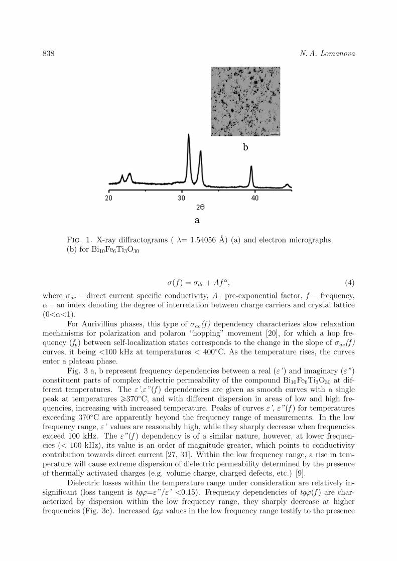
838 N.A. Lomanova
Fig. 1. X-ray diffractograms ( λ= 1.54056 A) (a) and electron micrographs(b) for Bi10Fe6Ti3O30
σ(f) = σdc + Afα, (4)
where σdc – direct current specific conductivity, A– pre-exponential factor, f – frequency,α – an index denoting the degree of interrelation between charge carriers and crystal lattice(0<α<1).
For Aurivillius phases, this type of σac(f) dependency characterizes slow relaxationmechanisms for polarization and polaron “hopping” movement [20], for which a hop fre-quency (fp) between self-localization states corresponds to the change in the slope of σac(f)curves, it being <100 kHz at temperatures < 400C. As the temperature rises, the curvesenter a plateau phase.
Fig. 3 a, b represent frequency dependencies between a real (ε’ ) and imaginary (ε”)constituent parts of complex dielectric permeability of the compound Bi10Fe6Ti3O30 at dif-ferent temperatures. The ε’,ε”(f ) dependencies are given as smooth curves with a singlepeak at temperatures >370C, and with different dispersion in areas of low and high fre-quencies, increasing with increased temperature. Peaks of curves ε’, ε”(f ) for temperaturesexceeding 370C are apparently beyond the frequency range of measurements. In the lowfrequency range, ε’ values are reasonably high, while they sharply decrease when frequenciesexceed 100 kHz. The ε”(f ) dependency is of a similar nature, however, at lower frequen-cies (< 100 kHz), its value is an order of magnitude greater, which points to conductivitycontribution towards direct current [27, 31]. Within the low frequency range, a rise in tem-perature will cause extreme dispersion of dielectric permeability determined by the presenceof thermally activated charges (e.g. volume charge, charged defects, etc.) [9].
Dielectric losses within the temperature range under consideration are relatively in-significant (loss tangent is tgϕ=ε”/ε’ <0.15). Frequency dependencies of tgϕ(f ) are char-acterized by dispersion within the low frequency range, they sharply decrease at higherfrequencies (Fig. 3c). Increased tgϕ values in the low frequency range testify to the presence
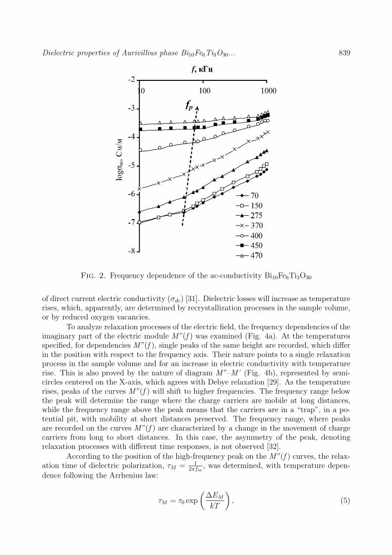
Dielectric properties of Aurivillius phase Bi10Fe6Ti3O30... 839
Fig. 2. Frequency dependence of the ac-conductivity Bi10Fe6Ti3O30
of direct current electric conductivity (σdc) [31]. Dielectric losses will increase as temperaturerises, which, apparently, are determined by recrystallization processes in the sample volume,or by reduced oxygen vacancies.
To analyze relaxation processes of the electric field, the frequency dependencies of theimaginary part of the electric module M”(f ) was examined (Fig. 4a). At the temperaturesspecified, for dependencies M”(f ), single peaks of the same height are recorded, which differin the position with respect to the frequency axis. Their nature points to a single relaxationprocess in the sample volume and for an increase in electric conductivity with temperaturerise. This is also proved by the nature of diagram M”–M’ (Fig. 4b), represented by semi-circles centered on the X-axis, which agrees with Debye relaxation [29]. As the temperaturerises, peaks of the curves M”(f ) will shift to higher frequencies. The frequency range belowthe peak will determine the range where the charge carriers are mobile at long distances,while the frequency range above the peak means that the carriers are in a “trap”, in a po-tential pit, with mobility at short distances preserved. The frequency range, where peaksare recorded on the curves M”(f ) are characterized by a change in the movement of chargecarriers from long to short distances. In this case, the asymmetry of the peak, denotingrelaxation processes with different time responses, is not observed [32].
According to the position of the high-frequency peak on the M”(f ) curves, the relax-ation time of dielectric polarization, τM = 1
2πfm, was determined, with temperature depen-
dence following the Arrhenius law:
τM = τ0 exp
(∆EMkT
), (5)
840 N.A. Lomanova
Fig. 3. Frequency dependence of the real, ε’ (a) and imaginary, ε”(b) partsof the dielectric permittivity (a, b) and dielectric, tgϕ, for Bi10Fe6Ti3O30, mea-sured at various temperatures
where τM is relaxation time in the grain volume determined by the peak of the curves M”(f),τ 0 is a pre-exponential factor, EM is energy of activation of the charge carriers in the grainvolume determined by the curve slope τM(1/T), k is Boltzmann constant, and T is absolutetemperature.
The relaxation time τ within the temperature range under consideration ranged from5·10−4–1·10−3 s. The activation energy EM of the charge carriers in the grain volume, esti-mated by ratio (5), was 0.8±0.1 eV, which is a typical value for compounds of Aurivilliusphases type [18-25], with electric conductivity determined, primarily, by oxygen vacancymovement. The presence of oxygen vacancies in the structure of bismuth-containing Au-rivillius phases is caused by the partial evaporation of Bi3+ ions under the high synthetictemperatures of these materials. This contributes to the overall electric conductivity, along
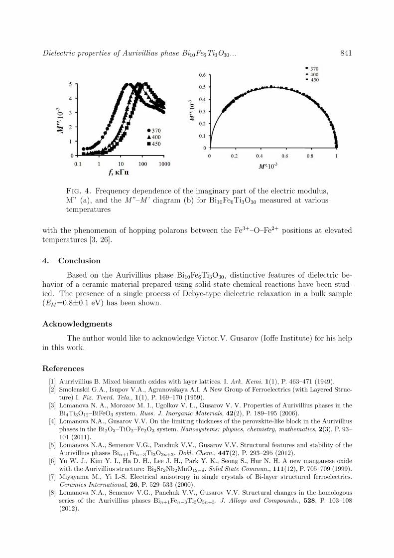
Dielectric properties of Aurivillius phase Bi10Fe6Ti3O30... 841
Fig. 4. Frequency dependence of the imaginary part of the electric modulus,M” (a), and the M”–M’ diagram (b) for Bi10Fe6Ti3O30 measured at varioustemperatures
with the phenomenon of hopping polarons between the Fe3+–O–Fe2+ positions at elevatedtemperatures [3, 26].
4. Conclusion
Based on the Aurivillius phase Bi10Fe6Ti3O30, distinctive features of dielectric be-havior of a ceramic material prepared using solid-state chemical reactions have been stud-ied. The presence of a single process of Debye-type dielectric relaxation in a bulk sample(EM=0.8±0.1 eV) has been shown.
Acknowledgments
The author would like to acknowledge Victor.V. Gusarov (Ioffe Institute) for his helpin this work.
References
[1] Aurrivillius B. Mixed bismuth oxides with layer lattices. I. Ark. Kemi. 1(1), P. 463–471 (1949).[2] Smolenskii G.A., Isupov V.A., Agranovskaya A.I. A New Group of Ferroelectrics (with Layered Struc-
ture) I. Fiz. Tverd. Tela., 1(1), P. 169–170 (1959).[3] Lomanova N. A., Morozov M. I., Ugolkov V. L., Gusarov V. V. Properties of Aurivillius phases in the
Bi4Ti3O12–BiFeO3 system. Russ. J. Inorganic Materials, 42(2), P. 189–195 (2006).[4] Lomanova N.A., Gusarov V.V. On the limiting thickness of the perovskite-like block in the Aurivillius
phases in the Bi2O3–TiO2–Fe2O3 system. Nanosystems: physics, chemistry, mathematics, 2(3), P. 93–101 (2011).
[5] Lomanova N.A., Semenov V.G., Panchuk V.V., Gusarov V.V. Structural features and stability of theAurivillius phases Bin+1Fen−3Ti3O3n+3. Dokl. Chem., 447(2), P. 293–295 (2012).
[6] Yu W. J., Kim Y. I., Ha D. H., Lee J. H., Park Y. K., Seong S., Hur N. H. A new manganese oxidewith the Aurivillius structure: Bi2Sr2Nb2MnO12−δ. Solid State Commun., 111(12), P. 705–709 (1999).
[7] Miyayama M., Yi I.-S. Electrical anisotropy in single crystals of Bi-layer structured ferroelectrics.Ceramics International, 26, P. 529–533 (2000).
[8] Lomanova N.A., Semenov V.G., Panchuk V.V., Gusarov V.V. Structural changes in the homologousseries of the Aurivillius phases Bin+1Fen−3Ti3O3n+3. J. Alloys and Compounds., 528, P. 103–108(2012).
842 N.A. Lomanova
[9] Bai W., Chen G., Zhu J. Y., Yang J., Lin T., Meng X.J., Tang X.D., Duan C.G., Chu J.H. Dielectricresponses and scaling behaviors in Aurivillius Bi6Ti3Fe2O18 multiferroic thin films. Appl. Phys. Lett.100(8), P. 082902–082906 (2012).
[10] Jiang P.P., Zhang X.L., Chang P., Hu Z. G., Bai W., W. Li Y., Chu J.H. Spin-phonon interactions ofmultiferroic Bi4Ti3O12-BiFeO3 ceramics: Low-temperature Raman scattering and infrared reflectancespectra investigations. J. Appl. Phys., 115, P. 144101–144106 (2014).
[11] Keeney L., Maity T., Schmidt M., Amann A., Deepak N., Petkov N., Roy S., Pemble M. E., WhatmoreR. W. J. Am. Ceram. Soc., 96(8), P. 2339–2357 (2013).
[12] Isupov V.A. Curie Temperatures of Am−1Bi2MmO3m+3 layered ferroelectrics Russ. J. Neorg. Mater.,33(9), . 1106–1110 (1997).
[13] Snedden A., Hervoches Ch. H., Lightfoot Ph. Ferroelectric phase transition in SrBi2Nb2O9 andBi15Ti3FeO15: a powder neutron diffraction study. Phys. Rew., 67, P. 092102 (2003).
[14] Krzhizhanovskya M., Filatov S., Gusarov V., Paufler P., Bubnova R., Morozov M., Meyer D. C.Aurivillius phases in the Bi4Ti3O12/BiFeO3 system: thermal behaviour and crystal structure. Z. Anorg.Allg. Chem., 631, P. 1603–1608 (2005).
[15] Subbanna G.N., Guru Row T.N., Rao C.N.R. Structure and dielectric properties of recurrent inter-growth structures formed by the Aurivillius family of bismuth oxides of the formula Bi2An−1BnO3n+3.J. Solid State Chem., 86(2), P. 206–211 (1990).
[16] Lomanova N.A., Ugolkov V. L., Gusarov V. V. Thermal behavior of layered perovskite-like compoundsin the Bi4Ti3O12–BiFeO3 system. Glass Physics and Chemistry, 33, P. 608–612 (2007).
[17] Lomanova N.A., Gusarov V.V. Phase states in the Bi4Ti3O12–BiFeO3 section in the Bi2O3–TiO2–Fe2O3 system. Russ. J. Inorg. Chem., 56, P. 616–620 (2011).
[18] Srinivas A., Kumar M., Suryanarayana S.V., Bhimasankaram T. Investigation of dielectric and mag-netic nature of Bi7Fe3Ti3O21. Mater. Res. Bull., 34(6), P. 989–996 (1999).
[19] Srinivas A., Kima Dong-Wan, Honga Kug Sun, Suryanarayana S.V. Study of magnetic and magneto-electric measurements in bismuth iron titanate ceramic-Bi8Fe4Ti3O24. Mater. Res. Bull., 39, P. 55–61(2004).
[20] Srinivas K., Sarah P., Suryanarayana S.V. Impedance spectroscopy study of polycrystallineBi6Fe2Ti3O18, Bull. Mater. Sci., 26(2), P. 247–253 (2003).
[21] Bucko M. M., Polnar J., Kozielski L. Dielectric Properties of Some Aurivillius Phases in the Bi4Ti3O12–BiFeO3 System. Materials Science Forum., 730, P. 88–93 (2013).
[22] Patwe S. J., Achary S. N., Manjanna J., Tyagi A. K., Deshpande S. K., Mishra S. K., Krishna P.S. R., Shinde A. B. Observation of a new cryogenic temperature dielectric relaxation in multiferroicBi7Fe3Ti3O21. Appl. Phys. Lett., 103, P. 12290–112296 (2013).
[23] Dercz J., Starczewska A., Dercz G. Dielectric and structural properties of Bi5Ti3FeO15 ceramics ob-tained by solid-state reaction process from mechanically activated precursors. Int. J. Thermophys., 32,P. 746–761 (2011).
[24] Lomanova N.A., Gusarov V.V. Electrical properties of perovskite-like compounds in the Bi2O3–TiO2–Fe2O3 system. Russ. J. Inorg. Mater., 47, P. 420–425 (2011).
[25] Lomanova N.A., Gusarov V.V. Impedance spectroscopy of polycrystalline materials based on the Auriv-illius phase system Bi4Ti3O12–BiFeO3. Nanosystems: physics, chemistry, mathematics, 3, P. 112–122(2012).
[26] Morozov M. I., Gusarov V.V. Synthesis of Am−1Bi2MmO3m+3 compounds in the Bi4Ti3O12–BiFeO3
system. Russ. J. Inorg. Mat., 38, P. 723–729 (2002).[27] Molak A., Paluch M., Pawlus S., Klimontko J., Ujma Z., Gruszka I. Electric modulus approach to the
analysis of electric relaxation in highly conducting (Na0.75Bi0.25)(Mn0.25Nb0.75)O3 ceramics. J. Phys.D: Appl. Phys., 38, P. 1450–1460 (2005).
[28] Yi Z. G., Li Y. X., Wang Y., Yin Q. R. Spectroscopies of mixed-layer Aurivillius phase Bi5Ti1.5W1.5O15
dielectric, impedance, and electric modulus. J. Electrochem. Soc., 153(6), P. F100–F105 (2006).[29] Jonscher A.K. The ‘universal’ dielectric response. Nature, 267, P. 673–679 (1977).[30] Jonscher A.K. Dielectric relaxation in solids. J. Phys. D: Appl. Phys., 32, P. R57–R70 (1999).[31] Gerhardt R. Impedance and dielectric spectroscopy revisited: Distinguishing localized relaxation from
long-range conductivity. J. Phys. Chem. Solids., 55, P. 1491–1506 (1994).[32] Pattanayak S., Parida B.N., Das P. R., Choudhary R.N.P. Impedance spectroscopy of Gd-doped
BiFeO3 multiferroics. Appl.Phys. A., 112, P. 387–395 (2013).

NANOSYSTEMS: PHYSICS, CHEMISTRY, MATHEMATICS, 2014, 5 (6), P. 843–848
SYNTHESIS AND STUDIES ROOM TEMPERATURECONDUCTIVITY, DIELECTRIC ANALYSIS
OF LaF3 NANOCRYSTALS
Sidheshwar G. Gaurkhede
Department of Physics, Bhavan’s College of ASC,Andheri (W) Mumbai-400058. India
PACS 61.05.cp, 77.22.d
Lanthanum fluoride (LaF3) was synthesized using LaCl3 and NH4F as starting materials in de-ionized water as
solvent via a microwave-assisted technique. The structure of LaF3 nanocrystals, analyzed by XRD and TEM,
was found to be hexagonal with an average crystalline particle size of 20 nm (JCPDS standard card (32-0483)
of pure hexagonal LaF3 crystals). The resistivity and conductivity at room temperature for LaF3 was verified
and found to depend on the applied DC field. At an applied voltage of 20 V/cm – 30 V/cm, the resistivity
and conductivity changes rapidly due to the liberation of extra fluoride (F−) ions, whereas the conductivity of
LaF3 nanocrystals depends upon temperature. The variation of dielectric constant (ε′) and dielectric loss (ε′′) with
applied frequency shows normal dielectric behavior, attributable to the space charge formation. The observed peak
in the plot of tangent loss (tan δ) vs. logF around 2.6 KHz can be attributed to interface charge relaxation at the
grain boundaries.
Keywords: Microwave radiation, Hexagonal shape, X-ray diffraction, Dielectric materials.
Received: 24 November 2014
Revised: 28 November 2014
1. Introduction
Lanthanum fluoride based chemical sensors have potential to be widely used in applica-tions such as the detection of fluorine, oxygen, and carbon monoxide, due to its high chemicalstability and ionic conductivity [1]. The ionic conducting nature of the rare earth fluorides(solid electrolyte) is exploited as sensor materials to construct various electrochemical sensorslike gas sensors, biosensors, and ion selective electrodes [2]. Lanthanum fluoride is an excellentF− ionic conductor among other rare earth fluorides [3]. Miura et al. reported the use oflanthanum fluoride film in biosensor and room-temperature oxygen sensor based on its highF− ion-conducting properties. The working principle of LaF3 based biosensors and oxygensensors is explained as the movement of F− ion conduction [4, 5]. Fedorov P. P. [6] et al. re-view the major aspects of inorganic chemistry of nanofluorides, methods of synthesis, includingnanochemical effects, preparation of 1D, 2D, and 3D nanostructures, surface modification ofthe nanoparticles, fluoride nanocomposites and applications of nanofluorides. The orthorhombicβ-YF3 structure and ionic conductivity of rare earth fluorides and of tysonite-structured wereinvestigated by Trnovcova et al. [7, 8]. At room temperature, the ionic conductivity of singlecrystals of tysonite-type solid solutions Lal−xBaxF3−x has been studied and no exchange occursbetween different types of anion sites in the tysonite structure [9, 10]. Very recently, Kumar etal. [11, 12] attempted to synthesize lanthanum fluoride nanoparticles by the simple method ofdirect precipitation in aqueous solution. The impedance, modulus and dielectric spectra analysis
844 Sidheshwar G. Gaurkhede
of the prepared LaF3 nanoparticles has been studied using AC impedance spectroscopy. Theionic conductivity of LaF3 nanoparticles were reported to be significantly increased by an orderof magnitude, from 10−6 S cm−1 to 10−5 S cm−1. The modulus and dielectric spectra analysisconfirmed the non-Debye type behavior in the material. The synthesized LaF3 nanoparticlesexhibited hexagonal shape and red luminescence. In the present case, LaF3 nanoparticles havebeen synthesized using a conventional microwave radiation technique for first time.
2. Experimental
2.1. Synthesis of Nanocrystals
Synthesis of LaF3 nanocrystals follows an aqueous route and uses a microwave heatingat low power range. The method is simple and cost effective. Water soluble LaCl3 and NH4Fare mixed to obtain a solution in 1:3 molar ratio [13]. To a 10 ml homogenous solution of0.64 mol LaCl3 in de-ionized water in a 100 ml beaker was added a 10 ml solution of 0.192 molNH4F in a drop-wise manner via a funnel fitted with a stopper to control the rate of dripping,and placed the whole set up inside a conventional microwave set at low power range (in on-offmode set at 30 sec) for around 30 min. The low power range setting largely helped us avoidspill-over of the solution. A white ultrafine crystalline precipitate identified as doped LaF3
nanocrystals appeared almost instantly, having settled to the bottom of the beaker. The whiteprecipitate was then washed several times with de-ionized water and absolute methanol, andwas then dried in a microwave oven for approximately 15 minutes. The dried sample was thenstored in sealed ampoules for further characterization and analysis.
2.2. Characterization
Powder X-ray diffraction (XRD) measurements have been performed using a PANA-LYTICAL X’PERT PROMPD diffractometer model using CuKα radiation λ = 1.5405 A. Uwith a scanning rate of 2 per min in the 2θ range from 0 to 80 . Transmission electronmicroscope (TEM) analysis was performed at different magnification by PHILIPS (CM 200)0.24 nm resolution, operating at 200 kV. The dielectric constants of the sample have been mea-sured using sophisticated Hioki 3532 LCR Meter. The capacitance and dissipation factor of theparallel plate capacitor formed by sample as a dielectric medium was measured.
3. Result and Discussion
The XRD pattern obtained from the LaF3 nanocrystals shown in Fig. 1. The results ofthe XRD are in good agreement with the hexagonal LaF3 structure as described in the reportsLaF3 (JCPDS card No. 32-0483) [14]. The average crystallite size was estimated from theScherrer equation, D = 0.90λ/β cos θ, where D is the average crystallite size, λ is the X-raywavelength (0.15405 nm), θ and β being the diffraction angle and full width at half maximumof an observed peak, respectively. The strongest peak (111) at θ = 27.84 for LaF3 sampleswere used to calculate the average crystallite size (D) of the nanoparticles [15]. The averagecrystallite sizes of LaF3 nanoparticles are 20 nm, which is in agreement with the TEM and SEMresults. The XRD pattern of the LaF3 nanoparticles is nearly similar to that of LaF3: Ce3+,Tb3+ [16]. No XRD signals are observed for impurity phases.
Figure 2 shows the transmission electron microscopy (TEM) image of LaF3 nanocrystals.Hexagonal, assorted and spherical shape nanocrystals with average particle size of about 21 nmwere found. Fig. 3 shows the selected area electron diffraction (SAED) pattern. Three strongdiffraction rings, corresponding to the (002), (111) and (300) reflections were observed, which
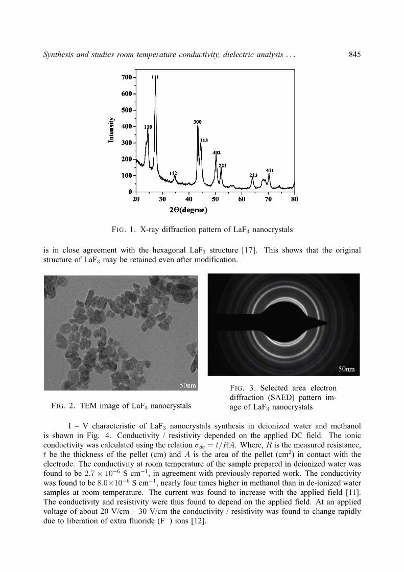
Synthesis and studies room temperature conductivity, dielectric analysis . . . 845
FIG. 1. X-ray diffraction pattern of LaF3 nanocrystals
is in close agreement with the hexagonal LaF3 structure [17]. This shows that the originalstructure of LaF3 may be retained even after modification.
FIG. 2. TEM image of LaF3 nanocrystals
FIG. 3. Selected area electrondiffraction (SAED) pattern im-age of LaF3 nanocrystals
I – V characteristic of LaF3 nanocrystals synthesis in deionized water and methanolis shown in Fig. 4. Conductivity / resistivity depended on the applied DC field. The ionicconductivity was calculated using the relation σdc = t/RA. Where, R is the measured resistance,t be the thickness of the pellet (cm) and A is the area of the pellet (cm2) in contact with theelectrode. The conductivity at room temperature of the sample prepared in deionized water wasfound to be 2.7× 10⁻⁶ S cm−1, in agreement with previously-reported work. The conductivitywas found to be 8.0×10⁻⁶ S cm−1, nearly four times higher in methanol than in de-ionized watersamples at room temperature. The current was found to increase with the applied field [11].The conductivity and resistivity were thus found to depend on the applied field. At an appliedvoltage of about 20 V/cm – 30 V/cm the conductivity / resistivity was found to change rapidlydue to liberation of extra fluoride (F−) ions [12].

846 Sidheshwar G. Gaurkhede
FIG. 4. Current vs. Voltage graph of LaF3 nanocrystals prepared in (a) de-ionizedwater (b) methanol
FIG. 5. Variation of dielectric constant with logF for LaF3 nanocrystals preparedin (a) de-ionized water (b) methanol
The variations of dielectric constant in log frequency at room temperature for LaF3
nanocrystals prepared in de-ionized water and methanol have been studied. Fig. 5 and Fig. 6shows the plot of dielectric constant ε′ as a function of log frequency and the plot of dielectricloss ε′′ as a function of log frequency for LaF3 nanocrystals. Both dielectric constant anddielectric loss exhibited similar variation with frequency, both being inversely proportional tofrequency. This is normal dielectric behavior, that both ε′ and ε′′ decrease with increasingfrequency. The dielectric constant was found to fall more rapidly as compared to dielectric losswith applied frequency.
A plot of tan δ against logF is shown in Fig. 7. The relaxation peaks were found to lienear 2.6 KHz. From the figure, the peak in the low frequency region indicates the contributionof the real dielectric constant of the material due to the polarization [18].
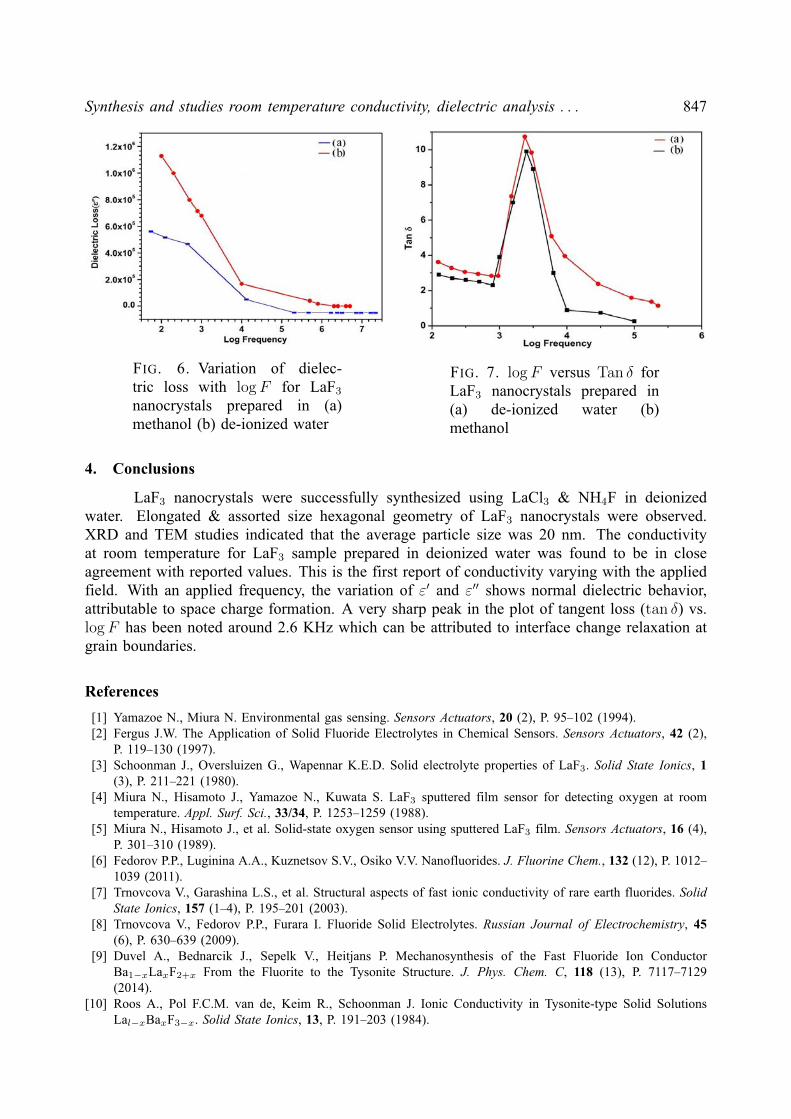
Synthesis and studies room temperature conductivity, dielectric analysis . . . 847
FIG. 6. Variation of dielec-tric loss with logF for LaF3
nanocrystals prepared in (a)methanol (b) de-ionized water
FIG. 7. logF versus Tan δ forLaF3 nanocrystals prepared in(a) de-ionized water (b)methanol
4. Conclusions
LaF3 nanocrystals were successfully synthesized using LaCl3 & NH4F in deionizedwater. Elongated & assorted size hexagonal geometry of LaF3 nanocrystals were observed.XRD and TEM studies indicated that the average particle size was 20 nm. The conductivityat room temperature for LaF3 sample prepared in deionized water was found to be in closeagreement with reported values. This is the first report of conductivity varying with the appliedfield. With an applied frequency, the variation of ε′ and ε′′ shows normal dielectric behavior,attributable to space charge formation. A very sharp peak in the plot of tangent loss (tan δ) vs.logF has been noted around 2.6 KHz which can be attributed to interface change relaxation atgrain boundaries.
References
[1] Yamazoe N., Miura N. Environmental gas sensing. Sensors Actuators, 20 (2), P. 95–102 (1994).[2] Fergus J.W. The Application of Solid Fluoride Electrolytes in Chemical Sensors. Sensors Actuators, 42 (2),
P. 119–130 (1997).[3] Schoonman J., Oversluizen G., Wapennar K.E.D. Solid electrolyte properties of LaF3. Solid State Ionics, 1
(3), P. 211–221 (1980).[4] Miura N., Hisamoto J., Yamazoe N., Kuwata S. LaF3 sputtered film sensor for detecting oxygen at room
temperature. Appl. Surf. Sci., 33/34, P. 1253–1259 (1988).[5] Miura N., Hisamoto J., et al. Solid-state oxygen sensor using sputtered LaF3 film. Sensors Actuators, 16 (4),
P. 301–310 (1989).[6] Fedorov P.P., Luginina A.A., Kuznetsov S.V., Osiko V.V. Nanofluorides. J. Fluorine Chem., 132 (12), P. 1012–
1039 (2011).[7] Trnovcova V., Garashina L.S., et al. Structural aspects of fast ionic conductivity of rare earth fluorides. Solid
State Ionics, 157 (1–4), P. 195–201 (2003).[8] Trnovcova V., Fedorov P.P., Furara I. Fluoride Solid Electrolytes. Russian Journal of Electrochemistry, 45
(6), P. 630–639 (2009).[9] Duvel A., Bednarcik J., Sepelk V., Heitjans P. Mechanosynthesis of the Fast Fluoride Ion Conductor
Ba1−xLaxF2+x From the Fluorite to the Tysonite Structure. J. Phys. Chem. C, 118 (13), P. 7117–7129(2014).
[10] Roos A., Pol F.C.M. van de, Keim R., Schoonman J. Ionic Conductivity in Tysonite-type Solid SolutionsLal−xBaxF3−x. Solid State Ionics, 13, P. 191–203 (1984).

848 Sidheshwar G. Gaurkhede
[11] Selvasekarapandiana S., Vijayakumara M., et al. Ion conduction studies on LaF3 thin film by impedancespectroscopy. Physica B, 337 (5), P. 52–57 (2003).
[12] Kumar D.A., Selvasekarapandian S., Nithya H., Hema M. Synthesis, micro-structural, and electrical analysison lanthanum fluoride. Ionics, 18 (5), P. 461–471 (2012).
[13] Meng J., Zhang M., Liu Y. Hydrothermal preparation and luminescence of LaF3:Eu3+ nanoparticles. Spect.Acta A, 66 (1), P. 81–85 (2007).
[14] Daihua T., Liu X., Zhen Z. Oleic acid (OA)-modified LaF3 : Er, Yb nanocrystals and their polymer hybridmaterials for potential optical-amplification applications. J. Mater. Chem., 17 (1), P. 1597–1601 (2007).
[15] Daqin C., Yuansheng W., En Ma, Yunlong Y. Influence of Yb3+ content on microstructure and fluorescenceof oxyfluoride glass ceramics containing LaF3 nano-crystals. Mater. Chem. Phys., 101 (9), P. 464–469 (2007).
[16] Pi D., Wang F., et al. Polyol-mediated synthesis of water-soluble LaF3:Yb,Er upconversion fluorescentnanocrystals. Materials Letters, 61 (6), P. 1337–1340 (2007).
[17] Yuanfang L., Wei C., et al. X-ray Luminescence of LaF3:Tb and LaF3:Ce, Tb Water Soluble Nanoparticles.J. Appl. Phys., 103 (6), P. 1–7 (2008).
[18] Kumar D.A., Selvasekarapandian S., et al. Dielectric, modulus and impedance analysis of LaF3 nanoparticles.Physica B: Condensed Matter, 405 (17), P. 3803–3807 (2010).

NANOSYSTEMS: PHYSICS, CHEMISTRY, MATHEMATICS, 2014, 5 (6), P. 849–853
POROUS STRUCTURE OF CARBONNANOPARTICLES PREPARED
BY CHLORINATION OF NANOPARTICLESOF SILICON CARBID
V. V. Sokolov, N. A. Petrov, M. V. Tomkovich, V. V. Gusarov
Ioffe Institute, 26 Polytekhnicheskaya Str., Saint Petersburg 194021, Russia
PACS 81.05.Uw; 61.46.-w
Specific features of the structure of nanoporous carbon, prepared by chlorinating silicon carbide nanoparticles
followed by treatment thereof by hydrogenation have been studied. A considerable number of microscopic
pores in carbon nanoparticles have been shown.
Keywords: nanoporous carbon, carbon nanoparticles.
Received: 20 November 2014
Revised: 5 December 2014
1. Introduction
Properties of carbon materials with effective surface are attributable both to thequantity of specific surface, and to their structure, including morphology, size, and porousstructure of nanoparticles.
Carbon materials with high surface area having micro-, meso-, and macropores basedon particles of micron and submicron dimensions are known and widely applied.
The synthesis of new substances, based on highly-porous carbon opens promisingprospects for the use of these materials and carbon-based nanocomposites as sorbents and gasaccumulators, catalysts in producing super-condensers, electrodes for electric-chemical gen-erators, etc. One of the promising classes of porous carbon materials is based on nanoporouscarbon prepared by high-temperature chlorination of carbides [1, 2]. In papers devoted tothe synthesis and study of nanoporous carbon, carbide powders of micron or submicrondimensions were chlorinated [1-4].
The study of the porous structure of carbon nanoparticles synthesized by chlorinatingcarbide powders is of interest. This article analyzes the porous structure of carbon nanopar-ticles synthesized by high-temperature chlorination of silicon carbide nanoparticles of cubicmodification ( SiC).
2. Experimental
For the synthesis of carbon nanoparticles, silicon carbide nanopowder primarily con-sisting of particles SiC (maximum content of amorphous phase 3-15%), with specific gravity3.22 g/cm3, spherical shape, 45–55 nm in diameter produced by Aldrich (USA) was em-ployed. Silicon carbide was chlorinated in a Tamman furnace under chlorine atmosphereat 700 to 1000C for 10 and 60 minutes. To remove chlorine impurities from the sampleaccording to the procedure described in [3], after chlorination, the sample was exposed tothermal hydrogenation at 800C for 60 minutes.
850 V.V. Sokolov, N.A. Petrov, et al.
Reliable data on the structure of nanoscale objects can only be obtained by em-ploying a comprehensive approach [5]. This requirement also applies to the analysis of theformed materials’ porous structure. Therefore, to define the structure and dimensions ofnanoparticles, as well as parameters for their porous structure, a variety of techniques wereemployed.
Parameters for the crystal structure of the sample were determined based on powderX-Ray diffraction data using a Shimadzu XRD-7000. Crystallites dimensions were calculatedaccording to Scherrer formula based on data from X-Ray diffraction line broadening.
Pycnometric specific gravity of powders was measured using a helium pycnometerAccuPyc 1330 (Micromeritics, USA).
Adsorption and structural analysis of powders were carried out using an analyzerASAP 2020 (Micromeritics, USA). Specific gravity of nanoparticles, cumulative pore volume,and distribution of pores by dimensions were calculated according to the model BET usingDFT method [6], included in the analyzer software. These methods, like others, suggest thatthe pores have a particular shape. Therefore, the results obtained for spherical, cylindrical,and slot-like pores or pore space of mixed type may vary widely [7].
This paper suggested that slot-like pores are most prevalent. Despite ambiguity, thismodel was chosen following the results of papers [2-4].
3. Results and discussion
Diffraction patterns of the samples under investigation (Fig. 1) show that for theinitial silicon carbide, consisting of nanocrystals SiC with diameters of d=20±2 nm (Ta-ble 1), the carbon synthesized by high-temperature chlorination will be amorphous. On thecontrary, for the carbon prepared by chlorination of macrocrystalline σSiC, the diffractionpatterns show the broadened lines similar in position to the graphite pattern lines [4].
Table 2 provides elemental composition of samples of nanoporous carbon prepared bychlorination of nanopowder SiC under different conditions. The data obtained show that thesamples contain insignificant quantities of oxygen and chlorine. In the sample chlorinated at700C, low silicon content was observed. Silicon is apparently present as SiO2. The presenceof silicon dioxide is likely attributable to the presence of impurities of silicon dioxide inthe initial sample, and to the stability of SiO2 under a chlorine atmosphere at 700C. Toremove chlorine impurities, the samples were treated under hydrogen atmosphere. Thetreatment ensured almost complete chlorine removal, see Table 2. Then, the nanoporouscarbon samples, once dechlorinated via hydrogenation, were then analyzed.
Table 3 gives the values for the specific surface area and parameters of porous struc-ture for nanoporous carbon samples prepared under different conditions for the chlorinationof SiC nanopowder. It should be noted that the results of the structural and adsorptionanalysis obtained for models BET and DFT vary widely (Table 3). The difference is mostpronounced in nanoporous carbon samples synthesized at higher temperatures, i.e. at 850and 1000C. This can be proved by the data on micropore volumes and cumulative pore vol-umes provided in Table 3, as well as the by the data on distribution of pores by dimensionsin nanoporous carbon prepared at different temperatures. Note that the presence of poreswith dimensions of 37 nm is apparently attributable to interparticle porosity. The poresshare dimensions for all chlorination conditions, because initial nanoparticles SiC were of50–60 nm in size (Table 1), chlorination did not cause considerable change in the dimensionsof the carbon particles as compared to the particles of the initial silicon carbide [7].
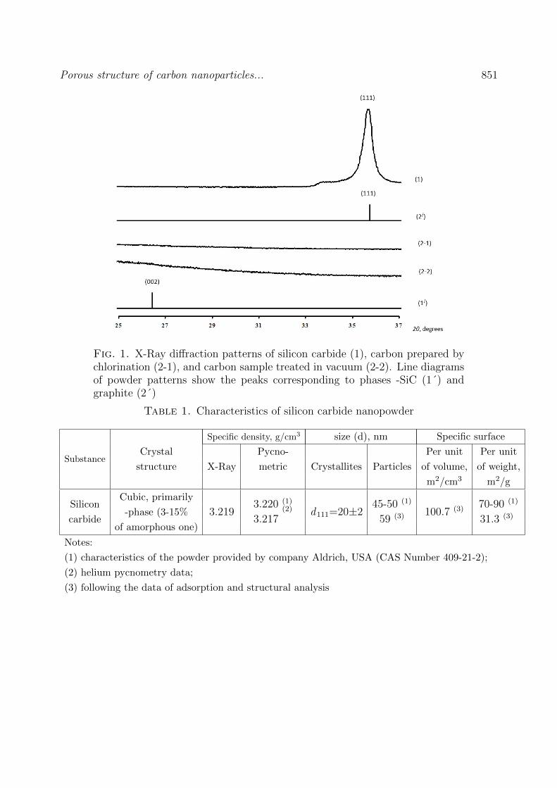
Porous structure of carbon nanoparticles... 851
Fig. 1. X-Ray diffraction patterns of silicon carbide (1), carbon prepared bychlorination (2-1), and carbon sample treated in vacuum (2-2). Line diagramsof powder patterns show the peaks corresponding to phases -SiC (1´) andgraphite (2´)
Table 1. Characteristics of silicon carbide nanopowder
Specific density, g/cm3 size (d), nm Specific surface
SubstanceCrystal Pycno- Per unit Per unit
structure X-Ray metric Crystallites Particles of volume, of weight,
m2/cm3 m2/g
SiliconCubic, primarily
3.220 (1) 45-50 (1) 70-90 (1)
carbide-phase (3-15% 3.219
3.217(2) d111=20±2
59 (3) 100.7 (3)
31.3 (3)
of amorphous one)
Notes:
(1) characteristics of the powder provided by company Aldrich, USA (CAS Number 409-21-2);
(2) helium pycnometry data;
(3) following the data of adsorption and structural analysis
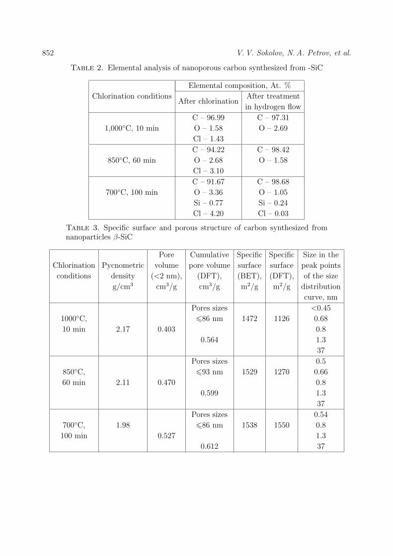
852 V.V. Sokolov, N.A. Petrov, et al.
Table 2. Elemental analysis of nanoporous carbon synthesized from -SiC
Elemental composition, At. %
Chlorination conditionsAfter chlorination
After treatment
in hydrogen flow
C – 96.99 C – 97.31
1,000C, 10 min O – 1.58 O – 2.69
Cl – 1.43
C – 94.22 C – 98.42
850C, 60 min O – 2.68 O – 1.58
Cl – 3.10
C – 91.67 C – 98.68
700C, 100 min O – 3.36 O – 1.05
Si – 0.77 Si – 0.24
Cl – 4.20 Cl – 0.03
Table 3. Specific surface and porous structure of carbon synthesized fromnanoparticles β-SiC
Pore Cumulative Specific Specific Size in the
Chlorination Pycnometric volume pore volume surface surface peak points
conditions density (<2 nm), (DFT), (BET), (DFT), of the size
g/cm3 cm3/g cm3/g m2/g m2/g distribution
curve, nm
Pores sizes <0.45
1000C, 686 nm 1472 1126 0.68
10 min 2.17 0.403 0.8
0.564 1.3
37
Pores sizes 0.5
850C, 693 nm 1529 1270 0.66
60 min 2.11 0.470 0.8
0.599 1.3
37
Pores sizes 0.54
700C, 1.98 686 nm 1538 1550 0.8
100 min 0.527 1.3
0.612 37
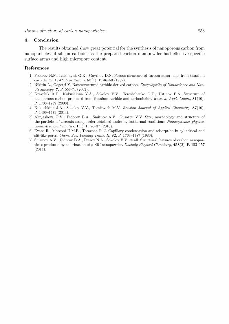
Porous structure of carbon nanoparticles... 853
4. Conclusion
The results obtained show great potential for the synthesis of nanoporous carbon fromnanoparticles of silicon carbide, as the prepared carbon nanopowder had effective specificsurface areas and high micropore content.
References
[1] Fedorov N.F., Ivakhnyuk G.K., Gavrilov D.N. Porous structure of carbon adsorbents from titaniumcarbide. Zh.Prikladnoi Khimii, 55(1), P. 46–50 (1982).
[2] Nikitin A., Gogotsi Y. Nanostructured carbide-derived carbon. Encyclopedia of Nanoscience and Nan-otechnology, 7, P. 553-74 (2003).
[3] Kravchik A.E., Kukushkina Y.A., Sokolov V.V., Tereshchenko G.F., Ustinov E.A. Structure ofnanoporous carbon produced from titanium carbide and carbonitride. Russ. J. Appl. Chem., 81(10),P. 1733–1739 (2008).
[4] Kukushkina J.A., Sokolov V.V., Tomkovich M.V. Russian Journal of Applied Chemistry, 87(10),P. 1466–1473 (2014).
[5] Almjasheva O.V., Fedorov B.A., Smirnov A.V., Gusarov V.V. Size, morphology and structure ofthe particles of zirconia nanopowder obtained under hydrothermal conditions. Nanosystems: physics,chemistry, mathematics, 1(1), P. 26–37 (2010).
[6] Evans R., Marconi U.M.B., Tarazona P. J. Capillary condensation and adsorption in cylindrical andslit-like pores. Chem. Soc. Faraday Trans. II, 82, P. 1763–1787 (1986).
[7] Smirnov A.V., Fedorov B.A., Petrov N.A., Sokolov V.V. et all. Structural features of carbon nanopar-ticles produced by chlorination of β-SiC nanopowder. Doklady Physical Chemistry, 458(2), P. 153–157(2014).
NANOSYSTEMS: PHYSICS, CHEMISTRY, MATHEMATICS, 2014, 5 (6), P. 854–860
NANOCRYSTALLINE PEROVSKITE-LIKE OXIDESFORMATION IN Ln2O3 – Fe2O3 – H2O
(Ln = La, Gd) SYSTEMS
E. A. Tugova, O. N. Karpov
Ioffe Physical Technical Institute of RAS, Saint Petersburg, Russia
PACS 61.46.-w; 82.80.Ej
Nanocrystalline LnFeO3 (Ln = La, Gd) ferrites have been prepared by the co-precipitation method followed
by heat treatment in air. The formation mechanisms for LaFeO3 and GdFeO3 in Ln2O3 – Fe2O3 – H2O (Ln =
La, Gd) systems under the mentioned conditions are investigated. The phase interaction scheme, reflecting
ways which lead to the target, synthesis product yield, as well as the common tendency of LaFeO3 and
GdFeO3 formation mechanisms, are constructed. The mean sizes of coherent scattering regions of LaFeO3
and GdFeO3 were determined to be 30±3 and 40±4 nm, respectively.
Keywords: LnFeO3, ferrites, nanostructures, precipitation technique, phase formation, X-Ray diffraction.
Received: 5 November 2014
Revised: 27 November 2014
1. Introduction
Perovskite-like oxides, produced by different synthetic methods and having a varietyof structural peculiarities, possess a complex array of electric, magnetic, catalytic, thermal,and other properties being of interest, in terms of practical applications [1-20]. Conven-tionally, the most common technique for obtaining complex oxides, including perovskite-likephases, is the method of solid-state synthesis [21-23]. Usually, for solid-state synthesis, sim-ple oxides, carbonates, nitrates, oxalates, citrates or other salts of proper metals can be usedas reagents. To ensure stoichiometry of the compounds synthesized, definite composition ofgaseous medium can be prescribed, i.e. air, nitrogen, oxygen, hydrogen, etc. Despite a greatnumber of papers devoted to the solid-state synthesis of perovskite-like oxides and to researchinto the peculiarities of their structure and properties [12, 17-21], limited data on the forma-tion processes for perovskite-like oxides are available. There is also insufficient data on stateequilibria for Ln2O3 – Fe2O3 (Ln = La, Gd) systems, which include perovskite-like oxides.Additionally, since the composition of the substances determines their basic properties, thelack of the mentioned data may affect the preparation of materials based on perovskite-likeoxides with function-oriented characteristics.
Recently, the preparation of perovskite-like oxides using “soft chemistry” techniqueshas become of greater interest [24-25]. This is determined by the practical application ofnanomaterials with unique structure and properties prepared using “soft chemistry” tech-niques [26]. However, mechanisms for the formation of the considered compounds remainmostly unstudied, which is associated, inter alia, with a lack of reliable generalized data onstability regions, processes of decomposition of intermediate substances, typically, p-, d - andf -elements hydroxides resulting from the reactions of precipitation, hydrolysis, etc., i.e. thoseproceeding, primarily, in aqueous media. Shafer and Roy attempted to determine stability of
Nanocrystalline perovskite-like oxides formation... 855
rare-earth oxides and hydroxides in studying the state equilibria of Ln2O3 – H2O (Ln= La,Nd, Sm) systems [27]. Lanthanum oxide was found to differ from neodymium and samarium,primarily, in its greater tendency towards hydration. The authors were not able to deter-mine whether LaOOH monohydrate or La2O3 forms via the decomposition of lanthanumhydroxide, or its crystal structure. The authors of [28] studied the dehydration kinetics forGd(OH)3 obtained via hydrothermal conditions. The chemical transformations within theFe2O3 – H2O system within media of different pH and with different P -T -conditions wereinvestigated in [29, 30]. Papers [2, 5, 31] also discussed the formation of LaFeO3 during thedehydration of components of the La2O3 – Fe2O3 – H2O system. It has been reported thatfor the preparation of GdFeO3 nanoparticles using polyol technique, the authors obtainedan until-then unknown compound corresponding to the formula Gd3FeO6, extending thenumber of compounds formed in the Gd2O3-Fe2O3-H2O system [32].
Thus, in literature, there are a number of works concerning the study of nanocrys-talline perovskite-like oxides using “soft chemistry” techniques. However, to describe themechanisms of perovskite-like oxides formation using “soft chemistry” techniques requiresapplication of a comprehensive approach, taking into account information about phase equi-libria in the systems where perovskite-like oxides could form, and analysis of the impactchemical background could have on the formation of the synthetic targets.
Therefore, the data investigation aims at studying of the formation processes ofnanoscale perovskite-like oxides in Ln2O3 – Fe2O3 – H2O (Ln = La, Gd) systems differ-ing in synthetic prehistory.
2. Experimental
2.1. Synthesis procedure
LnFeO3 (Ln = La, Gd) samples were prepared the by precipitation method fromaqueous solutions of stoichiometric amounts of 1M Ln(NO3)3·6H2O and Fe(NO3)3·9H2O.Aqueous 10 wt.% NH4OH was used as the precipitating medium. To the NH4OH medium,the aqueous solutions of lanthanum, gadolinium and iron nitrates were added in a drop-wise manner by adjusting the pH value to 8–9. The co-precipitated mixtures were filteredimmediately after preparation to remove traces of NO−
3 ions. Samples were then dried atroom temperature in air. These initial mixtures were then pressed and calcined in air at500–900C for 3 h.
2.2. Characterization of prepared nanocrystalline perovskite-related oxides
The purity and crystal structure of LnFeO3 (Ln = La, Gd) samples were characterizedby powder X-ray diffraction (XRD) using Shimadzu XRD-7000 with monochromatic CuKα
radiation (λ= 154.178 pm). α-Al2O3 was used as an internal standard. Crystallite sizesof the obtained powders were calculated by the X-ray line broadening technique based onScherer’s formula.
The elemental composition and the composition of separate phases were analyzedby means of scanning electron microscopy (SEM) using Quanta 200, coupled with EDAXmicroprobe analyzer. The error in determining the elements content by this method varieswith the atomic number and equals to 0.3 mass% on average.
The IR spectroscopic investigations of samples were carried out on an FSM-1202Fourier-transform spectrometer from 400–4000 cm−1. Samples were prepared as KBr pellets.
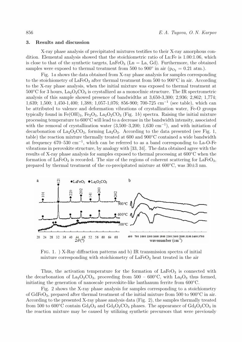
856 E.A. Tugova, O.N. Karpov
3. Results and discussion
X-ray phase analysis of precipitated mixtures testifies to their X-ray amorphous con-dition. Elemental analysis showed that the stoichiometric ratio of Ln:Fe is 1.00:1.06, whichis close to that of the synthetic targets, LnFeO3 (Ln = La, Gd). Furthermore, the obtainedsamples were exposed to thermal treatment from 500 to 900 in air (pO2 = 0.21 atm.).
Fig. 1a shows the data obtained from X-ray phase analysis for samples correspondingto the stoichiometry of LaFeO3 after thermal treatment from 500 to 900C in air. Accordingto the X-ray phase analysis, when the initial mixture was exposed to thermal treatment at500C for 3 hours, La2O2CO3 is crystallized as a monoclinic structure. The IR spectrometricanalysis of this sample showed presence of bandwidths at 3,650-3,300; 2,936; 2,862; 1,774;1,639; 1,500; 1,450-1,400; 1,388; 1,057-1,076; 856-900; 700-725 cm−1 (see table), which canbe attributed to valence and deformation vibrations of crystallization water, Fe-O groupstypically found in Fe(OH)3, Fe2O3, La2O2CO3 (Fig. 1b) spectra. Raising the initial mixtureprocessing temperature to 600C will lead to a decrease in the bandwidth intensity, associatedwith the removal of crystallization water (3,500–3,200; 1,630 cm−1), and with initiation ofdecarbonation of La2O2CO3, forming La2O3. According to the data presented (see Fig. 1,table) the reaction mixture thermally treated at 600 and 900C contained a wide bandwidthat frequency 670–530 cm−1, which can be referred to as a band corresponding to La-O-Fevibrations in perovskite structure, by analogy with [33, 34]. The data obtained agree with theresults of X-ray phase analysis for samples exposed to thermal processing at 600C when theformation of LaFeO3 is recorded. The size of the regions of coherent scattering for LaFeO3,prepared by thermal treatment of the co-precipitated mixture at 600C, was 30±3 nm.
Fig. 1. ) X-Ray diffraction patterns and b) IR transmission spectra of initialmixture corresponding with stoichiometry of LaFeO3 heat treated in the air
Thus, the activation temperature for the formation of LaFeO3 is connected withthe decarbonation of La2O2CO3, proceeding from 500 – 600C, with La2O3 thus formed,initiating the generation of nanoscale perovskite-like lanthanum ferrite from 600C.
Fig. 2 shows the X-ray phase analysis for samples corresponding to a stoichiometryof GdFeO3, prepared after thermal treatment of the initial mixture from 500 to 900C in air.According to the presented X-ray phase analysis data (Fig. 2), the samples thermally treatedfrom 500 to 600C contain Gd2O3 and Gd2O2CO3 phases. The appearance of Gd2O2CO3 inthe reaction mixture may be caused by utilizing synthetic precursors that were previously
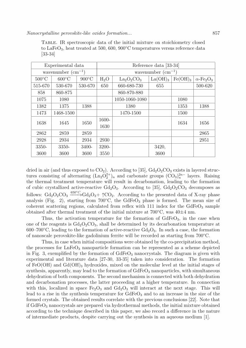
Nanocrystalline perovskite-like oxides formation... 857
Table. IR spectroscopic data of the initial mixture on stoichiometry closedto LaFeO3, heat treated at 500, 600, 900C temperatures versus reference data[33-34]
Experimental data Reference data [33-34]
wavenumber (cm−1) wavenumber (cm−1)
500C 600C 900C H2O La2O2CO3 La(OH)3 Fe(OH)3 α-Fe2O3
515-670 530-670 530-670 650 660-680-730 655 500-620
858 860-875 860-870-880
1075 1080 1050-1060-1080 1080
1382 1375 1388 1380 1353 1388
1473 1468-1500 1470-1500 1500
1638 1645 16501600-
1634 16561630
2862 2859 2859 2865
2928 2934 2934 2930 2951
3350- 3350- 3400- 3200- 3420,
3600 3600 3600 3550 3600
dried in air (and thus exposed to CO2). According to [35], Gd2O2CO3 exists in layered struc-tures consisting of alternating (Ln2O
2+2 )n and carbonate groups (CO3)
2n−n layers. Raising
the thermal treatment temperature will result in decarbonation, leading to the formationof cubic crystallized active-reactive Gd2O3. According to [35], Gd2O2CO3 decomposes as
follows: Gd2O2CO3650C−−−→Gd2O3+ ↑CO2. According to the presented data of X-ray phase
analysis (Fig. 2), starting from 700C, the GdFeO3 phase is formed. The mean size ofcoherent scattering regions, calculated from reflex with 111 index for the GdFeO3 sampleobtained after thermal treatment of the initial mixture at 700C, was 40±4 nm.
Thus, the activation temperature for the formation of GdFeO3, in the case whenone of the reagents is Gd2O2CO3, shall be determined by its decarbonation temperature at600–700C, leading to the formation of active-reactive Gd2O3. In such a case, the formationof nanoscale perovskite-like gadolinium ferrite will be recorded as starting from 700C.
Thus, in case when initial compositions were obtained by the co-precipitation method,the processes for LnFeO3 nanoparticle formation can be represented as a scheme depictedin Fig. 3, exemplified by the formation of GdFeO3 nanocrystals. The diagram is given withexperimental and literature data [27-30, 33-35] taken into consideration. The formationof FeO(OH) and Gd(OH)3 hydroxides, mixed on the molecular level at the initial stages ofsynthesis, apparently, may lead to the formation of GdFeO3 nanoparticles, with simultaneousdehydration of both components. The second mechanism is connected with both dehydrationand decarbonation processes, the latter proceeding at a higher temperature. In connectionwith this, localized in space Fe2O3 and Gd2O3 will interact at the next stage. This willlead to a rise in the synthesis temperature for GdFeO3 and to an increase in the size of theformed crystals. The obtained results correlate with the previous conclusions [22]. Note thatif GdFeO3 nanocrystals are prepared via hydrothermal methods, the initial mixture obtainedaccording to the technique described in this paper, we also record a difference in the natureof intermediate products, despite carrying out the synthesis in an aqueous medium [1].

858 E.A. Tugova, O.N. Karpov
Fig. 2. X-Ray diffraction patterns of initial mixtures corresponding with sto-ichiometry of GdFeO3 after sintering within the temperature range 500 to900C in the air
Fig. 3. LnFeO3 nanocrystals formation scheme exemplified by the formingof GdFeO3 under the heat treatment of co-precipitated initial mixture in airRemarks: I - the mechanism of co-precipitated hydroxides simultaneous de-hydration with GdFeO3 formation; II - the scheme of step-by-step transfor-mations of co-precipitated components with spatial-isolated Fe2O3 and Gd2O3
nanoparticles formation followed by solid state interaction for GdFeO3 pro-duction
Nanocrystalline perovskite-like oxides formation... 859
4. Conclusion
Therefore, the mechanism for perovskite-related lanthanum and gadolinium ferritesformation depends heavily on chemical processes resulting in the spatial separation of com-ponents of a target product. In particular, these processes may determine the temperature atwhich perovskite-related ferrite begins to form, as well as the size of the formed nanocrystals.
Acknowledgments
The authors would like to thank Prof. V.V. Gusarov very much for useful discussionsand valuable advice.
References
[1] Tugova E.A., Zvereva I.A. Formation mechanism of GdFeO3 nanoparticles under the hydrothermalconditions. Nanosystems: physics, chemistry, mathematics, 4(6), P. 851–856 (2013).
[2] Nakayama S. LaFeO3 perovskite type oxide prepared by oxide mixing co-precipitation and complexsynthesis methods. J. Mater. Sci., 6, P. 5643–5648 (2001).
[3] Tang P., Chen H., Cao F., Pan G. Magnetically recoverable and visible light driven nanocrystallineYFeO3 photocatalysts. Catal. Sci. Technol., 1(7), P. 1145–1148 (2011).
[4] Nguyen A.T., Mittova I.Ya., Al’myasheva O.V. Influence of the synthesis conditions on the particlesize and morphology of yttrium orthoferrite obtained from aqueous solutions. Russ. J. Appl. Chem.,82(11), P. 1915–1918 (2009).
[5] Nguyen A.T., Mittova I.Ya., Almjasheva O.V., Kirillova S.A., Gusarov V.V. Influence of the prepa-ration conditions on the size and morphology of nanocrystalline lanthanum orthoferrite. Glas. Phys.Chem., 34(6), P. 756–761 (2008).
[6] Shang M., Zhang C., Zhang T., Yuan L., Ge L. Yuan H., Feng S. The multiferroic perovskite YFeO3.Appl. Phys. Lett., 102(6), 062903(3 pages) (2013).
[7] Zhou Z., Guo L., Yang H., Liu Q., Ye F. Hydrothermal synthesis and magnetic properties of multiferroicrare-earth orthoferrites. J. Alloys Compd, 583, P. 21–31 (2014).
[8] Tang P., Sun H., Chen H., Cao F. Hydrothermal processing-assisted synthesis of nanocrystalline YFeO3
and its visible-light photocatalytic activity. Curr. Nanosci., 8, P. 64–67 (2012).[9] Nguyen A.T., Almjasheva O.V., Mittova I.Ya., Stognei O.V., Soldatenko S.A. Synthesis and magnetic
properties of YFeO3 nanocrystals. Inorganic Materials, 45(11), P. 1304–1308 (2009).[10] Zhang Yu., Yang J., Xu J., Gao Q., Hong Zh. Controllable synthesis of hexagonal and orthorhombic
YFeO3 and their visible-light photocatalytic activities. Materials Letters, 81, P. 1–4 (2012).[11] Maiti R., Basu S., Chakravorty D. Synthesis of nanocrystalline YFeO3 and its magnetic properties.
Journal of Magnetism and Magnetic Materials, 321(19), P. 3274–3277 (2009).[12] Venugopalan A., Appasamy M., Saravanan S., Kothandaraman K., Kothandaraman J. Structural,
electrical and magnetic studies on Y-Fe-O system. Journal of Rare Earths, 27(6), P. 1013–1017 (2009).[13] Lu X., Xie J., Shu H., Liu J., Yin Ch., Lin J. Microwave-assisted synthesis of nanocrystalline YFeO3
and study of its photoactivity. Materials Science and Engineering B, 138, P. 289–292 (2007).[14] Zhang W., Fang C.X, Yin W.H, Zeng Y.W. One-step synthesis of yttrium orthoferrite nanocrystals
via sol-gel auto-combustion and their structural and magnetic characteristics. Mater. Chem. Phys.,137(3), P. 877–883 (2013).
[15] Popkov V.I., Almjasheva O.V. Yttrium orthoferrite YFeO3 nanopowders formation under glycine-nitrate combustion conditions. Russian Journal of Applied Chemistry, 87(2), P. 167–171 (2014).
[16] Goswami S., Bhattacharya D., Choudhury P. Particle size dependence on magnetization and noncen-trosymmetry in nanoscale BiFeO3. Journal of applied physics D, 109(7), P. 737–739 (2011).
[17] Egorysheva A.V., Volodin V.D., Ellert O.G., Efimov N.N., Skorikov V.M., Baranchikov A.E., Novo-tortsev V.M. Mechanochemical activation of starting oxide mixtures for solid-state synthesis of BiFeO3.Inorganic Materials, 49(3), P. 303–309 (2013).
[18] Morozov M. I., Lomanova N. A., Gusarov V.V. Specific features of BiFeO3 formation in a mixture ofbismuth (III) and iron (III) oxides. Russ. J. Gen. Chem., 73(11), P. 1772–1776 (2003).
[19] Lomanova N.A., Gusarov V.V. Effect of surface melting on the formation and growth of nanocrystalsin the Bi2O3-Fe2O3 system. Russ. J. Gen. Chem., 83(12), P. 2251–2253 (2013).
860 E.A. Tugova, O.N. Karpov
[20] Lomanova N.A., Gusarov V.V. Influence of synthesis temperature on BiFeO3 nanoparticles formation.Nanosystems: physics, chemistry, mathematics, 4(5), P. 696–705 (2013).
[21] Tretyakov Yu. D., Lukashin A.V., Eliseev A. A. Synthesis of functional nanocomposites based onsolid-phase nanoreactors. Russian Chemical Reviews, 73(9), P. 899–923 (2004).
[22] Gusarov V.V. Fast solid-phase chemical reactions. Russian Journal of General Chemistry, 67(12),P. 1846–1851 (1997).
[23] Schaak R.E., Mallouk Th. E. Perovskites by design: A toolbox of solid-state reactions. Chemistry ofMaterials, 14, P. 1455–1471 (2002).
[24] Livage J. Vanadium pentoxide gels. Chemistry of Materials, 3(4), P. 578–593 (1991).[25] Sanchez C., Rozes L., Ribot F., Laberty-Robert C., Grosso D., Sassoye C., Boissiere C., Nicole L.
“Chimie douce”: A land of opportunities for the designed construction of functional inorganic andhybrid organic-inorganic nanomaterials. Comptes Rendus Chimie, 13(1-2), P. 3–39 (2010).
[26] Gopalakrishnan J. Chimie. Douce approaches to the synthesis of metastable oxide materials. Chemistryof Materials, 7(7), P. 1265–1275 (1995).
[27] Shafer M.W., Roy R. Rare-earth polymorphism and phase equilibria in rare-earth oxide-water systems.Journal of the American Ceramic Society, 42(4), P. 563–570 (1959).
[28] Chang Ch, Mao D. Thermal dehydration kinetics of a rare earth hydroxide Gd(OH)3. InternationalJournal of Chemical Kinetics, 39(2), P. 75–81. (2007)
[29] Tareen J.A.K., Krishnamurthy K.V. Hydrothermal stability of hematite and magnetite. Bulletin Ma-terials Science, 3(1), P. 9–13 (1981).
[30] Popov, V.V., Gorbunov, A.I. Hydrothermal Crystallization of iron (III) hydroxide. Inorg. Materials,42(3), P. 275–281 (2006).
[31] Xu H., Hu X., Zhang L. Generalized low-temperature synthesis of nanocrystalline rare earth orthofer-rites LnFeO3 (Ln=La, Pr, Nd, Sm, Eu, Gd). Cryst. Growth Des., 8(7), P. 2061–2065 (2008).
[32] Soderlind S., Fortin M.A, Petoral Jr R.M., Klasson A., Veres T., Engstrom M., Uvdal K., Kall P.-O.Colloidal synthesis and characterization of ultrasmall perovskite GdFeO3 nanocrystals. Nanotechnol-ogy, 19(8), P. 085608-(8pp) (2008).
[33] Tugova E.A. A comparative analysis of the formation processes of Ruddlesden-Popper phases in theLa2O3-SrO-M2O3 (M = Al, Fe) systems. Glas. Phys. Chem, 35(4), P. 416–422 (2009).
[34] Bernal S., Blanco G., Gatica J.M., Perez-Omil J.A., Pintado J.M., Vidal H. Chemical reactivity ofbinary rare earth oxides. Binary Rare Earth Oxides, Kluwer Academic Publishers, P. 9–55 (2004).
[35] Sheu H. Sh., Shih W.-J., Chuang W.-T., Li I.-F., Yeh Ch.-Sh. Crystal structure and phase transitionsof Gd(CO3)OH studied by synchrotron powder diffraction. Journal of the Chinese Chemical Society,57(4), P. 938–945 (2010).
Information for authors 861
NANOSYSTEMS: PHYSICS, CHEMISTRY, MATHEMATICS
INFORMATION FOR AUTHORS
The journal publishes research articles and reviews, and also short scientific papers (letters) which are unpublished and have not been accepted for publication in other magazines. Articles should be submitted in English. All articles are reviewed, then if necessary come back to the author to completion.
The journal is indexed in Chemical Abstract Service of the American Chemical Society and in Russian Scientific Citation Index. Author should submit the following materials: 1. Article file in English, containing article title, the initials and the surname of the authors,
Institute (University), postal address, the electronic address, the summary, keywords, MSC or PACS index, article text, the list of references.
2. Files with illustrations, files with tables. 3. The covering letter in English containing the article information (article name, MSC or
PACS index, keywords, the summary, the literature) and about all authors (the surname, names, the full name of places of work, the mailing address with the postal code, contact phone number with a city code, the electronic address).
4. The expert judgement on possibility of publication of the article in open press (for authors from Russia).
Authors can submit a paper and the corresponding files to the following addresses: [email protected], [email protected]. Text requirements
Articles should be prepared with using of text editors MS Word or LaTEX (preferable). It is necessary to submit a pdf copy. In the name of files the English alphabet is used. The recommended size of short communications (letters) is 4-6 pages, research articles – 6-15 pages, reviews – 30 pages.
Recommendations for text in MS Word: Formulas should be written using Math Type. Figures and tables with captions should
be inserted in the text. Additionally, authors present separate files for all figures and Word files of tables.
N A N O
Ф &Х &М

Information for authors 862
Recommendations for text in LaTex: Please, use standard LaTex without macros and additional style files. The list of
references should be included in the main LaTex file. Single LaTex file of the paper with the corresponding pdf file should be submitted.
References in the article text are given in square brackets. The list of references should
be prepared in accordance with the following samples: [1] N. Surname. Book Title. Nauka Publishing House, Saint Petersburg, 281 pp. (2000). [2] N. Surname, N. Surname. Paper title. Journal Name, 1(5), P. 17-23 (2000). [3] N. Surname, N. Surname. Lecture title. In: Abstracts/Proceedings of the Conference,
Place and Date, P. 17-23 (2000). [4] N. Surname, N. Surname. Paper title (2010). URL: http://books.ifmo.ru/ntv. [5] N. Surname, N. Surname. Patent Name. Patent No. 11111, Bul. No. 33, 5 pp. (2010). [6] N. Surname, N. Surname. Thesis Title. Thesis for full doctor degree in math. and
physics, Saint Petersburg, 105 pp. (2000).
Requirements to illustrations Illustrations should be submitted as separate black-and-white files. Formats of files –
jpeg, eps, tiff.


NANOSYSTEMS: PHYSICS, CHEMISTRY, MATHEMATICS
Журнал зарегистрирован Федеральной службой по надзору в сфере связи, информационных технологий и массовых коммуникаций (свидетельство ПИ ФС 77 - 49048 от 22.03.2012 г.) ISSN 2220-8054 Учредитель: федеральное государственное автономное образовательное учреждение высшего образования «Санкт-Петербургский национальный исследовательский университет информационных технологий, механики и оптики» Издатель: федеральное государственное автономное образовательное учреждение высшего образования «Санкт-Петербургский национальный исследовательский университет информационных технологий, механики и оптики» Отпечатано в Учреждении «Университетские телекоммуникации» Адрес: 197101, Санкт-Петербург, Кронверкский пр., 49 Подписка на журнал НФХМ На второе полугодие 2015 года подписка осуществляется через ОАО Агентство «Роспечать» Подписной индекс 57385 в каталоге «Издания органов научно-технической информации»
N A N O
Ф &Х &М