Embed Size (px)
Citation preview
Physics of Failure Analysis of Xilinx Flip chip CCGA Packages
Jong-ook Suh, Shri Agarwal, Peter Dillon, Doug Sheldon
Jet Propulsion Laboratory, California Institute of Technology
NASA Electronic Parts and Packaging Program (NEPP)
3rd Annual NEPP Electronic Technology Workshop (ETW)
June 11-13th, 2012
To be presented by Jong-ook Suh at the NASA Electronic Parts and Packaging Program (NEPP) Electronics Technology Workshop (ETW), NASA Goddard Space Flight Center in Greenbelt, MD, June 11-13, 2012 and published on nepp.nasa.gov
© 2012 California Institute of Technology. Government sponsorship acknowledged.
Outline
1. Background
2. Approach
3. Results
4. Current status of the task and future plans.
5. Summary
To be presented by Jong-ook Suh at the NASA Electronic Parts and Packaging Program (NEPP) Electronics Technology Workshop
(ETW), NASA Goddard Space Flight Center in Greenbelt, MD, June 11-13, 2012 and published on nepp.nasa.gov
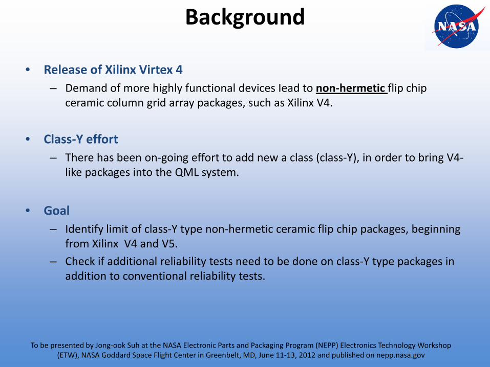
Background
• Release of Xilinx Virtex 4 – Demand of more highly functional devices Iead to non-hermetic flip chip
ceramic column grid array packages, such as Xilinx V4.
• Class-Y effort – There has been on-going effort to add new a class (class-Y), in order to bring V4-
like packages into the QML system.
• Goal – Identify limit of class-Y type non-hermetic ceramic flip chip packages, beginning
from Xilinx V4 and V5.
– Check if additional reliability tests need to be done on class-Y type packages in addition to conventional reliability tests.
To be presented by Jong-ook Suh at the NASA Electronic Parts and Packaging Program (NEPP) Electronics Technology Workshop (ETW), NASA Goddard Space Flight Center in Greenbelt, MD, June 11-13, 2012 and published on nepp.nasa.gov
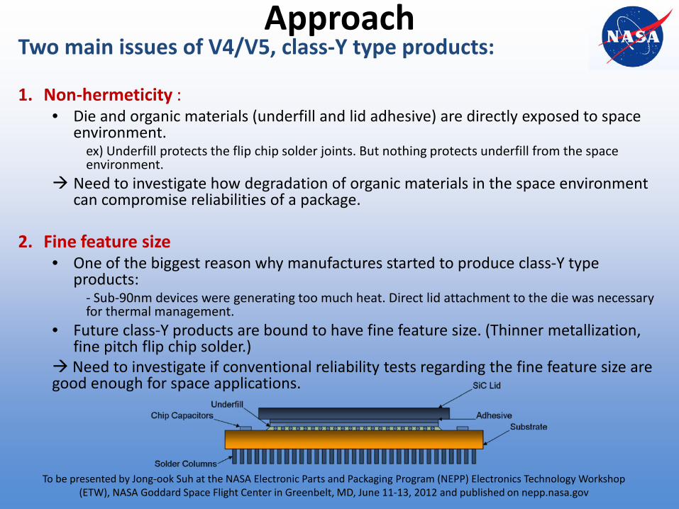
Approach Two main issues of V4/V5, class-Y type products:
1. Non-hermeticity :
• Die and organic materials (underfill and lid adhesive) are directly exposed to space environment.
ex) Underfill protects the flip chip solder joints. But nothing protects underfill from the space environment.
Need to investigate how degradation of organic materials in the space environment can compromise reliabilities of a package.
2. Fine feature size • One of the biggest reason why manufactures started to produce class-Y type
products: - Sub-90nm devices were generating too much heat. Direct lid attachment to the die was necessary for thermal management.
• Future class-Y products are bound to have fine feature size. (Thinner metallization, fine pitch flip chip solder.)
Need to investigate if conventional reliability tests regarding the fine feature size are good enough for space applications.
To be presented by Jong-ook Suh at the NASA Electronic Parts and Packaging Program (NEPP) Electronics Technology Workshop (ETW), NASA Goddard Space Flight Center in Greenbelt, MD, June 11-13, 2012 and published on nepp.nasa.gov
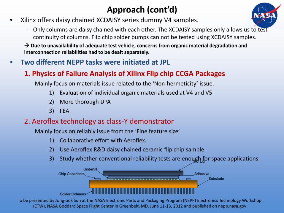
Approach (cont’d) • Xilinx offers daisy chained XCDAISY series dummy V4 samples.
– Only columns are daisy chained with each other. The XCDAISY samples only allows us to test continuity of columns. Flip chip solder bumps can not be tested using XCDAISY samples.
Due to unavailability of adequate test vehicle, concerns from organic material degradation and interconnection reliabilities had to be dealt separately.
• Two different NEPP tasks were initiated at JPL
1. Physics of Failure Analysis of Xilinx Flip chip CCGA Packages Mainly focus on materials issue related to the ‘Non-hermeticity’ issue.
1) Evaluation of individual organic materials used at V4 and V5
2) More thorough DPA
3) FEA
2. Aeroflex technology as class-Y demonstrator Mainly focus on reliably issue from the ‘Fine feature size’
1) Collaborative effort with Aeroflex.
2) Use Aeroflex R&D daisy chained ceramic flip chip sample.
3) Study whether conventional reliability tests are enough for space applications.
To be presented by Jong-ook Suh at the NASA Electronic Parts and Packaging Program (NEPP) Electronics Technology Workshop (ETW), NASA Goddard Space Flight Center in Greenbelt, MD, June 11-13, 2012 and published on nepp.nasa.gov
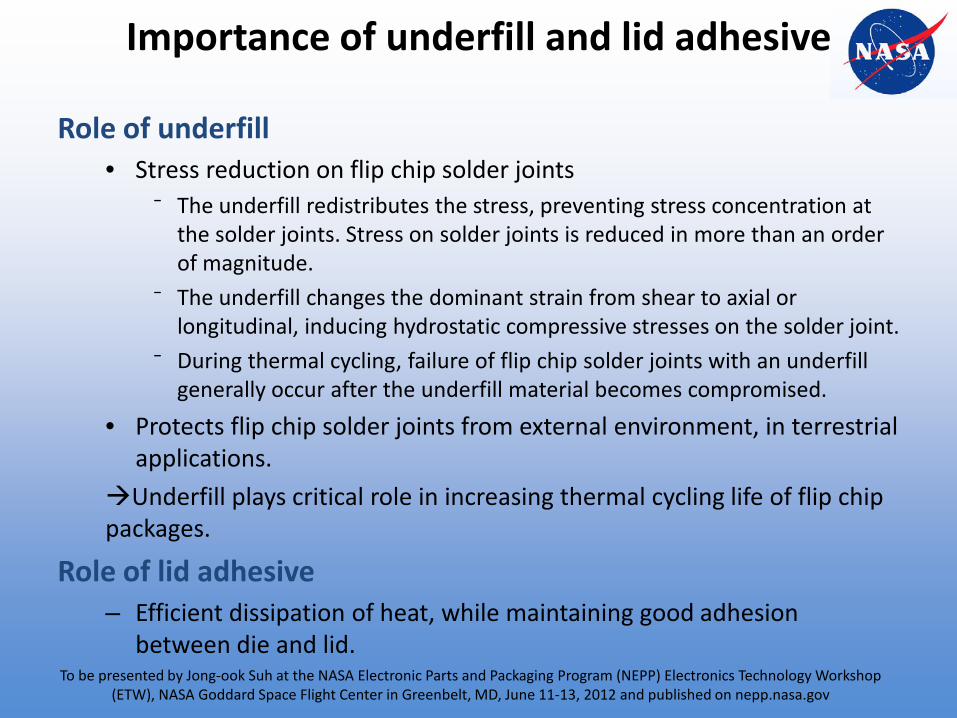
Importance of underfill and lid adhesive
Role of underfill • Stress reduction on flip chip solder joints
⁻ The underfill redistributes the stress, preventing stress concentration at the solder joints. Stress on solder joints is reduced in more than an order of magnitude.
⁻ The underfill changes the dominant strain from shear to axial or longitudinal, inducing hydrostatic compressive stresses on the solder joint.
⁻ During thermal cycling, failure of flip chip solder joints with an underfill generally occur after the underfill material becomes compromised.
• Protects flip chip solder joints from external environment, in terrestrial applications.
Underfill plays critical role in increasing thermal cycling life of flip chip packages.
Role of lid adhesive – Efficient dissipation of heat, while maintaining good adhesion
between die and lid.
To be presented by Jong-ook Suh at the NASA Electronic Parts and Packaging Program (NEPP) Electronics Technology Workshop (ETW), NASA Goddard Space Flight Center in Greenbelt, MD, June 11-13, 2012 and published on nepp.nasa.gov
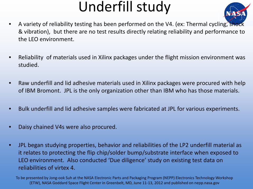
Underfill study • A variety of reliability testing has been performed on the V4. (ex: Thermal cycling, shock
& vibration), but there are no test results directly relating reliability and performance to the LEO environment.
• Reliability of materials used in Xilinx packages under the flight mission environment was studied.
• Raw underfill and lid adhesive materials used in Xilinx packages were procured with help of IBM Bromont. JPL is the only organization other than IBM who has those materials.
• Bulk underfill and lid adhesive samples were fabricated at JPL for various experiments.
• Daisy chained V4s were also procured.
• JPL began studying properties, behavior and reliabilities of the LP2 underfill material as it relates to protecting the flip chip/solder bump/substrate interface when exposed to LEO environment. Also conducted ‘Due diligence’ study on existing test data on reliabilities of virtex 4.
To be presented by Jong-ook Suh at the NASA Electronic Parts and Packaging Program (NEPP) Electronics Technology Workshop
(ETW), NASA Goddard Space Flight Center in Greenbelt, MD, June 11-13, 2012 and published on nepp.nasa.gov
To be presented by Jong-ook Suh at the NASA Electronic Parts and Packaging Program (NEPP) Electronics Technology Workshop (ETW), NASA Goddard Space Flight Center in Greenbelt, MD, June 11-13, 2012 and published on nepp.nasa.gov
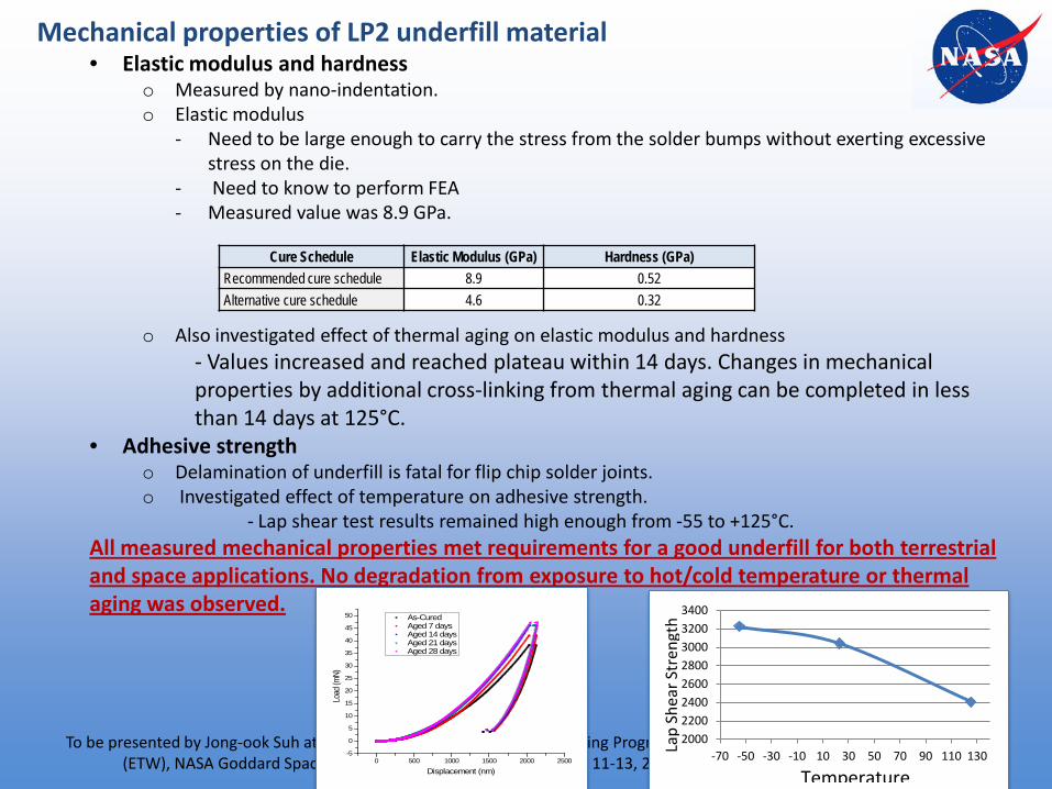
Mechanical properties of LP2 underfill material • Elastic modulus and hardness
o Measured by nano-indentation. o Elastic modulus
- Need to be large enough to carry the stress from the solder bumps without exerting excessive stress on the die.
- Need to know to perform FEA - Measured value was 8.9 GPa.
o Also investigated effect of thermal aging on elastic modulus and hardness
- Values increased and reached plateau within 14 days. Changes in mechanical properties by additional cross-linking from thermal aging can be completed in less than 14 days at 125°C.
• Adhesive strength o Delamination of underfill is fatal for flip chip solder joints. o Investigated effect of temperature on adhesive strength. - Lap shear test results remained high enough from -55 to +125°C.
All measured mechanical properties met requirements for a good underfill for both terrestrial and space applications. No degradation from exposure to hot/cold temperature or thermal aging was observed.
0 500 1000 1500 2000 2500-5
0
5
10
15
20
25
30
35
40
45
50 As-Cured Aged 7 days Aged 14 days Aged 21 days Aged 28 days
Load
(mN)
Displacement (nm)
Cure Schedule Elastic Modulus (GPa) Hardness (GPa) Recommended cure schedule 8.9 0.52 Alternative cure schedule 4.6 0.32
2000 2200 2400 2600 2800 3000 3200 3400
-70 -50 -30 -10 10 30 50 70 90 110 130
Temperature
Lap
Shea
r Str
engt
h

Thermal properties and behavior of LP2 underfill material • Glass transition temperature
o Properties of a polymer material (i.e, CTE, elastic modulus, electrical impedance) dramatically change at the glass transition temperature (Tg)
o It is desirable for underfill materials to have Tg outside the operating temperature range of the package. (ex: higher than +125°C)
o Measured with differential scanning calorimetry (DSC), thermomechanical analysis (TMA), and Dynamic mechanical analysis (DMA).
o As long as the underfill material was cured under recommended cure condition, the measured Tg was higher than +130°C.
(The junction temperature will be significantly higher than the temperature of underfill.)
• Coefficient of thermal expansion o Measured with TMA. o Ideally, CTE of underfill material should be close to or slightly higher than the
CTE of the solder. (CTE of 95Pb5Sn is 29.0 ppm/°C ) o Measured CTE was 21.27 ppm/°C.
• Thermal degradation o Measured with thermogravimetric analysis (TGA) o Onset of weight loss transition was at 373.94°C
Tg and CTE values were satisfactory.
To be presented by Jong-ook Suh at the NASA Electronic Parts and Packaging Program (NEPP) Electronics Technology Workshop (ETW), NASA Goddard Space Flight Center in Greenbelt, MD, June 11-13, 2012 and published on nepp.nasa.gov
TemperatureD
imen
sion
Cha
nge
α= 21.27μm/(m·°C)
α= 75.46 μm/(m·°C)
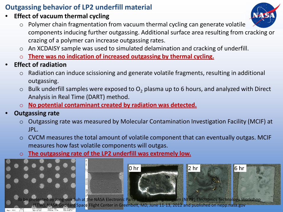
Outgassing behavior of LP2 underfill material • Effect of vacuum thermal cycling
o Polymer chain fragmentation from vacuum thermal cycling can generate volatile components inducing further outgassing. Additional surface area resulting from cracking or crazing of a polymer can increase outgassing rates.
o An XCDAISY sample was used to simulated delamination and cracking of underfill. o There was no indication of increased outgassing by thermal cycling.
• Effect of radiation o Radiation can induce scissioning and generate volatile fragments, resulting in additional
outgassing. o Bulk underfill samples were exposed to O2 plasma up to 6 hours, and analyzed with Direct
Analysis in Real Time (DART) method. o No potential contaminant created by radiation was detected.
• Outgassing rate o Outgassing rate was measured by Molecular Contamination Investigation Facility (MCIF) at
JPL. o CVCM measures the total amount of volatile component that can eventually outgas. MCIF
measures how fast volatile components will outgas. o The outgassing rate of the LP2 underfill was extremely low.
To be presented by Jong-ook Suh at the NASA Electronic Parts and Packaging Program (NEPP) Electronics Technology Workshop (ETW), NASA Goddard Space Flight Center in Greenbelt, MD, June 11-13, 2012 and published on nepp.nasa.gov
Electrical behavior • Volume resistivity
o Measured with standard resistivity cell, on 75μm thick LP2 material spin-coated to N+ type 4-inch silicon wafer.
o Measured volume resistivity was 3.92×10¹⁵ ohm-cm.
• Possibility of arcing due to radiation o There have been questions among some members of the space community,
based on their experiences with printed circuit board encapsulation, as to whether or not there is any likelihood radiation may induce arcing of the underfill.
o Dielectric materials for space applications are recommended to have a minimum conductivity, in order to minimize the risk of arcing. (resistivity below 1015 ohm-cm.)
o Even though the resistivity of LP2 material is higher than 1015 ohm-cm, the risk of radiation charging and arcing is low, because the geometry of the package will prevent the LP2 underfill material from charging.
- In the case of very thin materials surrounded by thick materials, the energetic electrons or protons either are stopped by other materials before they reach the material or pass through it entirely.
To be presented by Jong-ook Suh at the NASA Electronic Parts and Packaging Program (NEPP) Electronics Technology Workshop (ETW), NASA Goddard Space Flight Center in Greenbelt, MD, June 11-13, 2012 and published on nepp.nasa.gov

LEO environment tests on underfill and lid adhesive • Most of the tests were done under atmospheric pressure.
- Mechanical properties • Elastic modulus and hardness
o Effect of thermal aging • Adhesive strength
o Effect of temperature - Thermal properties and behavior
• Thermal degradation • Glass transition temperature • Coefficient of thermal expansion
- Outgassing behavior • Effect of vacuum thermal cycling • Effect of radiation • Outgassing rate
- Electrical behavior • Volume resistivity • Possibility of arcing due to radiation
• Reliabilities of materials in Xilinx packages under the LEO environment are being investigated.
• There are various constituents of the LEO environment.
- Vacuum, ionizing radiation, atomic oxygen, UV radiation.. - High vacuum was determined to be the most relevant and realistic issue for the class-Y
type packages.
To be presented by Jong-ook Suh at the NASA Electronic Parts and Packaging Program (NEPP) Electronics Technology Workshop (ETW), NASA Goddard Space Flight Center in Greenbelt, MD, June 11-13, 2012 and published on nepp.nasa.gov
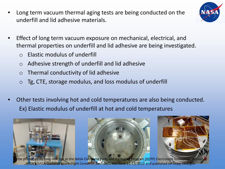
• Long term vacuum thermal aging tests are being conducted on the underfill and lid adhesive materials.
• Effect of long term vacuum exposure on mechanical, electrical, and thermal properties on underfill and lid adhesive are being investigated.
o Elastic modulus of underfill
o Adhesive strength of underfill and lid adhesive
o Thermal conductivity of lid adhesive
o Tg, CTE, storage modulus, and loss modulus of underfill
• Other tests involving hot and cold temperatures are also being conducted.
Ex) Elastic modulus of underfill at hot and cold temperatures
To be presented by Jong-ook Suh at the NASA Electronic Parts and Packaging Program (NEPP) Electronics Technology Workshop (ETW), NASA Goddard Space Flight Center in Greenbelt, MD, June 11-13, 2012 and published on nepp.nasa.gov
Summary
• JPL has been investigating reliability issues of Xilinx flip chip CCGA packages in terms of underfill and lid adhesive materials.
• The LP2 underfill material did not show any critical weakness from tests done under atmospheric pressure.
• Long term vacuum exposure experiments on underfill and lid adhesive material are being conducted.
To be presented by Jong-ook Suh at the NASA Electronic Parts and Packaging Program (NEPP) Electronics Technology Workshop (ETW), NASA Goddard Space Flight Center in Greenbelt, MD, June 11-13, 2012 and published on nepp.nasa.gov