Embed Size (px)
Citation preview
NREL is a national laboratory of the U.S. Department of Energy, Office of Energy Efficiency and Renewable Energy, operated by the Alliance for Sustainable Energy, LLC.
Physics of Failure of Electrical Interconnects
PI: Douglas DeVoto National Renewable Energy Laboratory May 15, 2012
Project ID: APE036
This presentation does not contain any proprietary, confidential, or otherwise restricted information.
2
Overview
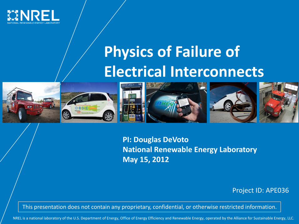
Timeline Project Start Date: FY11 Project End Date: FY13 Percent Complete: 40%
Barriers and Targets • Efficiency • Performance and Lifetime
Budget Total Project Funding: DOE Share: $600K
Funding Received in FY11: $300K Funding for FY12: $300K
Partners • Interactions/ Collaborations
• Curamik, Materion Technical Materials, Orthodyne Electronics
• Project lead: NREL
3
Relevance/Objectives
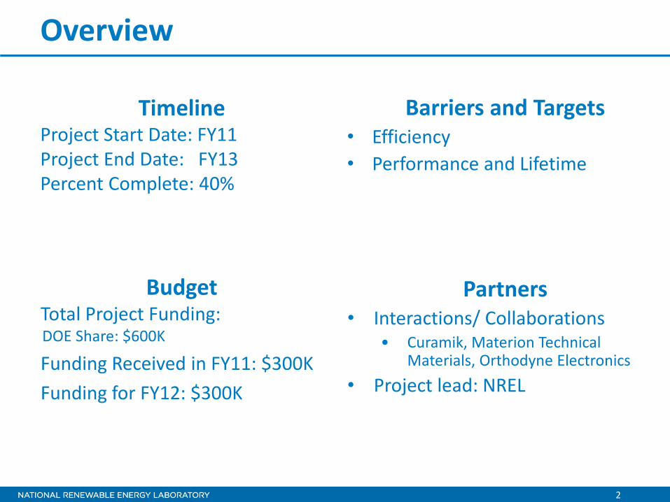
• Traditional interconnect technologies, such as wire bonding, do not sufficiently meet the needs of the latest power inverters, which function at high frequencies, high power densities, and elevated temperatures.
• Present electrical interconnect technology has limited current-carrying capability.
• Elevated temperatures (>150°C) and temperature cycling can degrade the performance and reliability of interconnects.
• The package size of power modules is being reduced and requires more spatially efficient interconnects.
4
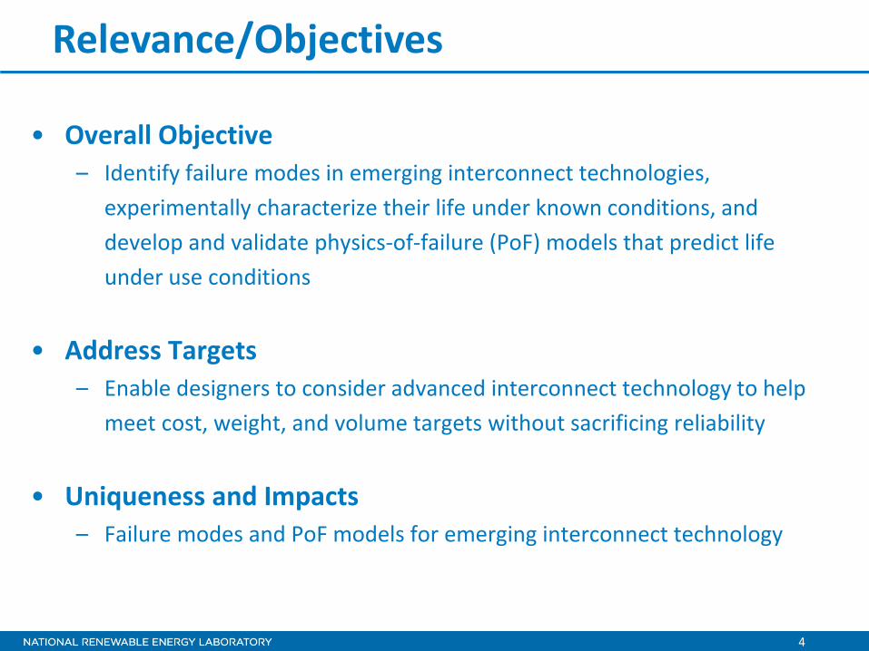
Relevance/Objectives
• Overall Objective – Identify failure modes in emerging interconnect technologies,
experimentally characterize their life under known conditions, and develop and validate physics-of-failure (PoF) models that predict life under use conditions
• Address Targets – Enable designers to consider advanced interconnect technology to help
meet cost, weight, and volume targets without sacrificing reliability
• Uniqueness and Impacts – Failure modes and PoF models for emerging interconnect technology
5
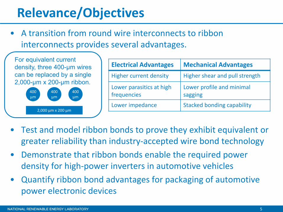
Relevance/Objectives • A transition from round wire interconnects to ribbon
interconnects provides several advantages.
• Test and model ribbon bonds to prove they exhibit equivalent or greater reliability than industry-accepted wire bond technology
• Demonstrate that ribbon bonds enable the required power density for high-power inverters in automotive vehicles
• Quantify ribbon bond advantages for packaging of automotive power electronic devices
400 µm
2,000 µm x 200 µm
400 µm
400 µm
For equivalent current density, three 400-µm wires can be replaced by a single 2,000-µm x 200-µm ribbon.
Electrical Advantages Mechanical Advantages Higher current density Higher shear and pull strength
Lower parasitics at high frequencies
Lower profile and minimal sagging
Lower impedance Stacked bonding capability
6
Milestones
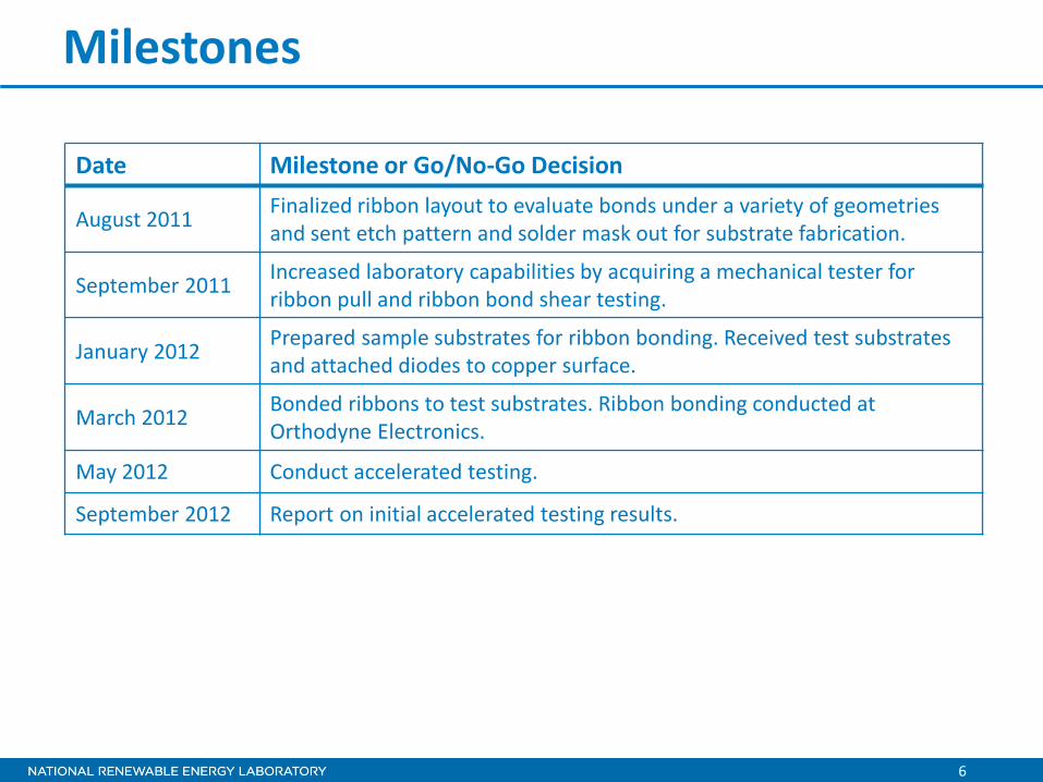
Date Milestone or Go/No-Go Decision
August 2011 Finalized ribbon layout to evaluate bonds under a variety of geometries and sent etch pattern and solder mask out for substrate fabrication.
September 2011 Increased laboratory capabilities by acquiring a mechanical tester for ribbon pull and ribbon bond shear testing.
January 2012 Prepared sample substrates for ribbon bonding. Received test substrates and attached diodes to copper surface.
March 2012 Bonded ribbons to test substrates. Ribbon bonding conducted at Orthodyne Electronics.
May 2012 Conduct accelerated testing.
September 2012 Report on initial accelerated testing results.
7
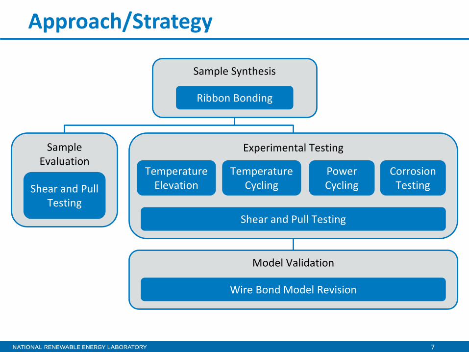
Approach/Strategy
Sample Synthesis
Ribbon Bonding
Sample Evaluation
Shear and Pull Testing
Experimental Testing
Temperature Elevation
Temperature Cycling
Power Cycling
Corrosion Testing
Shear and Pull Testing
Model Validation
Wire Bond Model Revision
8
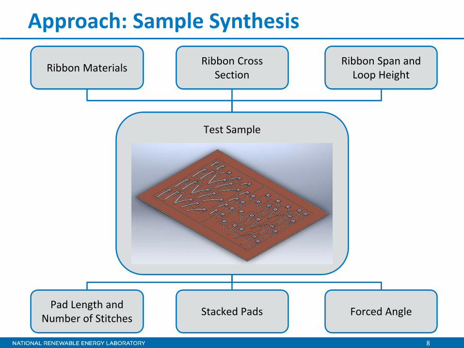
Approach: Sample Synthesis
Test Sample
Ribbon Materials Ribbon Cross Section
Ribbon Span and Loop Height
Pad Length and Number of Stitches Stacked Pads Forced Angle
9
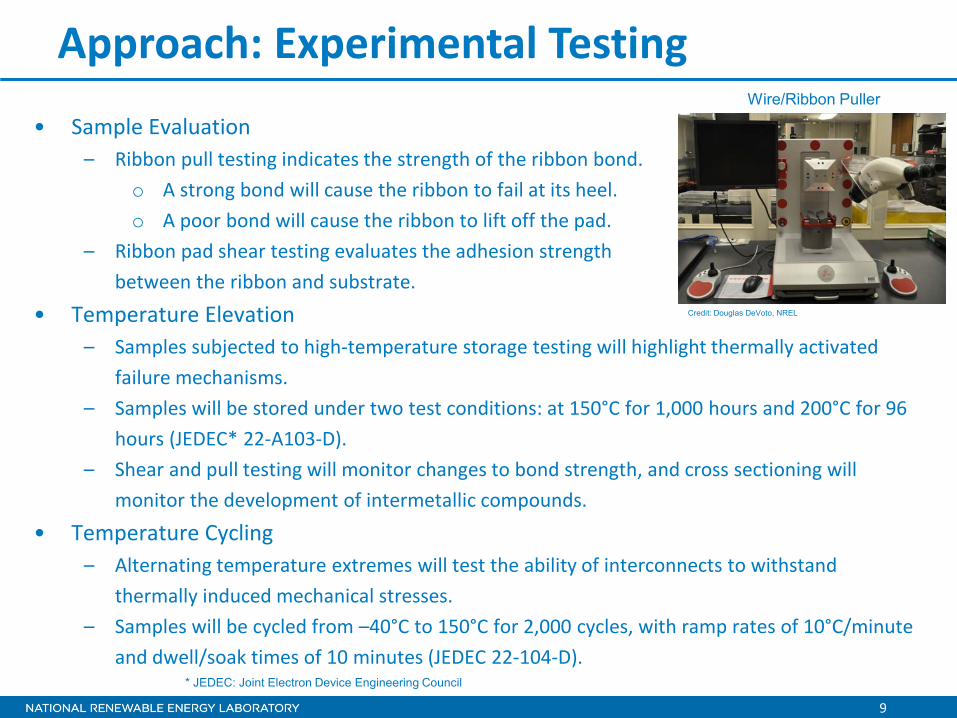
Approach: Experimental Testing
• Sample Evaluation – Ribbon pull testing indicates the strength of the ribbon bond.
o A strong bond will cause the ribbon to fail at its heel. o A poor bond will cause the ribbon to lift off the pad.
– Ribbon pad shear testing evaluates the adhesion strength between the ribbon and substrate.
• Temperature Elevation – Samples subjected to high-temperature storage testing will highlight thermally activated
failure mechanisms. – Samples will be stored under two test conditions: at 150°C for 1,000 hours and 200°C for 96
hours (JEDEC* 22-A103-D). – Shear and pull testing will monitor changes to bond strength, and cross sectioning will
monitor the development of intermetallic compounds. • Temperature Cycling
– Alternating temperature extremes will test the ability of interconnects to withstand thermally induced mechanical stresses.
– Samples will be cycled from –40°C to 150°C for 2,000 cycles, with ramp rates of 10°C/minute and dwell/soak times of 10 minutes (JEDEC 22-104-D).
Wire/Ribbon Puller
Credit: Douglas DeVoto, NREL
* JEDEC: Joint Electron Device Engineering Council
10
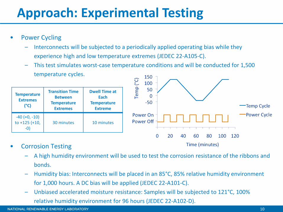
Approach: Experimental Testing
• Power Cycling – Interconnects will be subjected to a periodically applied operating bias while they
experience high and low temperature extremes (JEDEC 22-A105-C). – This test simulates worst-case temperature conditions and will be conducted for 1,500
temperature cycles.
• Corrosion Testing – A high humidity environment will be used to test the corrosion resistance of the ribbons and
bonds. – Humidity bias: Interconnects will be placed in an 85°C, 85% relative humidity environment
for 1,000 hours. A DC bias will be applied (JEDEC 22-A101-C). – Unbiased accelerated moisture resistance: Samples will be subjected to 121°C, 100%
relative humidity environment for 96 hours (JEDEC 22-A102-D).
Temperature Extremes
(°C)
Transition Time Between
Temperature Extremes
Dwell Time at Each
Temperature Extreme
-40 (+0, -10) to +125 (+10,
-0) 30 minutes 10 minutes
11
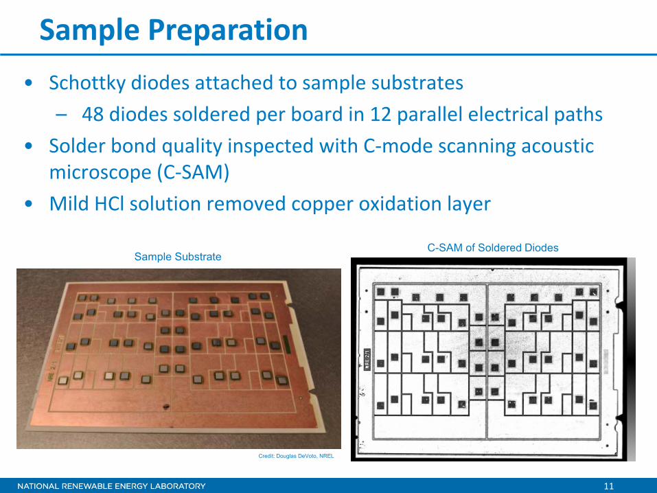
Sample Preparation
Sample Substrate C-SAM of Soldered Diodes
• Schottky diodes attached to sample substrates – 48 diodes soldered per board in 12 parallel electrical paths
• Solder bond quality inspected with C-mode scanning acoustic microscope (C-SAM)
• Mild HCl solution removed copper oxidation layer
Credit: Douglas DeVoto, NREL
12
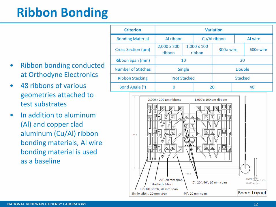
Ribbon Bonding
• Ribbon bonding conducted at Orthodyne Electronics
• 48 ribbons of various geometries attached to test substrates
• In addition to aluminum (Al) and copper clad aluminum (Cu/Al) ribbon bonding materials, Al wire bonding material is used as a baseline
Criterion Variation
Bonding Material Al ribbon Cu/Al ribbon Al wire
Cross Section (µm) 2,000 x 200
ribbon 1,000 x 100
ribbon 300⌀ wire 500⌀ wire
Ribbon Span (mm) 10 20
Number of Stitches Single Double
Ribbon Stacking Not Stacked Stacked
Bond Angle (°) 0 20 40
13
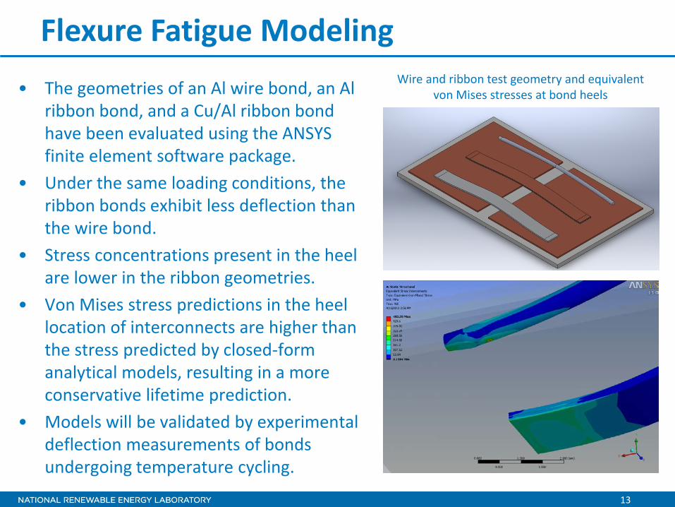
Flexure Fatigue Modeling Wire and ribbon test geometry and equivalent
von Mises stresses at bond heels • The geometries of an Al wire bond, an Al ribbon bond, and a Cu/Al ribbon bond have been evaluated using the ANSYS finite element software package.
• Under the same loading conditions, the ribbon bonds exhibit less deflection than the wire bond.
• Stress concentrations present in the heel are lower in the ribbon geometries.
• Von Mises stress predictions in the heel location of interconnects are higher than the stress predicted by closed-form analytical models, resulting in a more conservative lifetime prediction.
• Models will be validated by experimental deflection measurements of bonds undergoing temperature cycling.
14
Collaboration and Coordination
• Partners – Curamik (Industry): technical partner on substrate design – Materion Technical Materials (Industry): technical partner on ribbon
material – Orthodyne Electronics (Industry): technical partner on wire and
ribbon bonding procedure
15
Proposed Future Work (FY12)
• Determine ribbon bond strength through pull and shear tests • Complete thermal, power and environmental testing on
ribbon bonds • Report on mechanical reliability of ribbon bonds under
testing and make recommendations to industry partners • Update 2D wire bond models to be applicable for ribbon
bonds
16
Proposed Future Work (FY13)
• Perform reliability testing and develop PoF models for additional interconnect technologies, such as planar interconnects or flex foil
• Apply PoF models to a production module with ribbon bonding
17
Summary • DOE Mission Support
– Transitioning from wire bonding to ribbon bonding manufacturing will advance power electronics technology for compact, reliable packaging with higher current capabilities.
• Approach – Synthesis of ribbon bonds with varying material (Al, Cu/Al) and geometry
(cross section, span and loop height, pad length, number of stitches, stacked pads, and forced angles) parameters.
– Comprehensive reliability testing, including temperature elevation, temperature cycling, power cycling and corrosion testing.
– Revision of wire bond models to be applicable to ribbon bonding. • Accomplishments
– Industry partners have been selected for collaboration on ribbon bonding interconnect technology.
– Ribbon material and geometry have been selected for testing. – Test samples have been synthesized, and reliability testing has been
initiated.
18
Summary • Collaborations
– Curamik, Materion Technical Materials, Orthodyne Electronics • Future Work
– Determine ribbon bond strength through pull and shear tests – Complete thermal, power and environmental testing on ribbon bonds – Report on mechanical reliability of ribbon bonds under testing and make
recommendations to industry partners – Update 2D wire bond models to be applicable for ribbon bonds – Perform reliability testing and develop PoF models for additional
interconnect technologies, such as planar interconnects or flex foil – Apply PoF models to a production module with ribbon bonding
For more information contact:
Principal Investigator Douglas DeVoto [email protected] Phone: (303)-275-4256 APEEM Task Leader
Sreekant Narumanchi [email protected] Phone: (303)-275-4062
Acknowledgments:
Susan Rogers and Steven Boyd, U.S. Department of Energy Team Members:
Mark Mihalic