Embed Size (px)
Citation preview
|||||||||||||||||||||||||||||||||||||||||||||||||||||||||||||||||||||||||||||||||||||||||||||||||||||||||||||||||||||||||||||||||||||||||||||||||||||||||||||||||||||||||||||||||||||||||||||||||||||||||||||||||||||||||||||||||||||||||||||||||||||||||||||||||||||||||||||||||||||||||||||||||||||||||||||||||||||||||||||||||||||||
USB 2.0 Port Protection with Charger Detection
2014-04-0004 PT0502-1 04/28/14
1
PI3USB9281
Features
USB-device charger detector
Can tolerate USB3.0-PD with VBUS = 20V
USB Charging-type detection
Battery Charging 1.2 (BC1.2) – DCP
Battery Charging 1.2 (BC1.2) – CDP
Battery Charging 1.2 (BC1.2) – SDP
Apple 1A, 2A, & 2.4A dedicated chargers
Samsung-Fast chargers
YD/T-1951 dedicated chargers
CEA-936 Carkit#1 and #2 chargers
Integrated Power FET
VBUS Tolerance up to 28V
1.7A Over-Current Protection (OCP)
VBUS Over-Voltage Protection (OVP)
Non-charging Accessory Detection
USB On-The-Go (OTG) detection
Mobile HDMI Link (MHL) device detection
Wide Supply Voltage Range 3V to 5.5V
I2C Programmability
Small Package: CSP 1.5x2.0-15L
Applications
Personal Media Players
Mobile Phones
Tablet
Pin Configuration
Description
PI3USB9281 provides external detection for any USB-
device. The part can detect various chargers available in
the market, MHL accessories, OTG accessories, and car-
chargers per the CEA936 spec. It also integrates a power
switch with over-voltage and over-current protections.
The VBUSIN input pin can tolerate voltages up to 28V,
which is important for USB3.0-PowerDelivery enabled
ports. The new USB-3.0-PowerDelivery specification
supports voltages up to 20V.
The PI3USB9281 can operate over a temperature range
of -40 to +85°C.
Typical applications involve portable & consumer
applications, such as tablet, smart phones, digital
cameras, and notebooks with integrated Li-ion batteries
that charge via USB connectors.
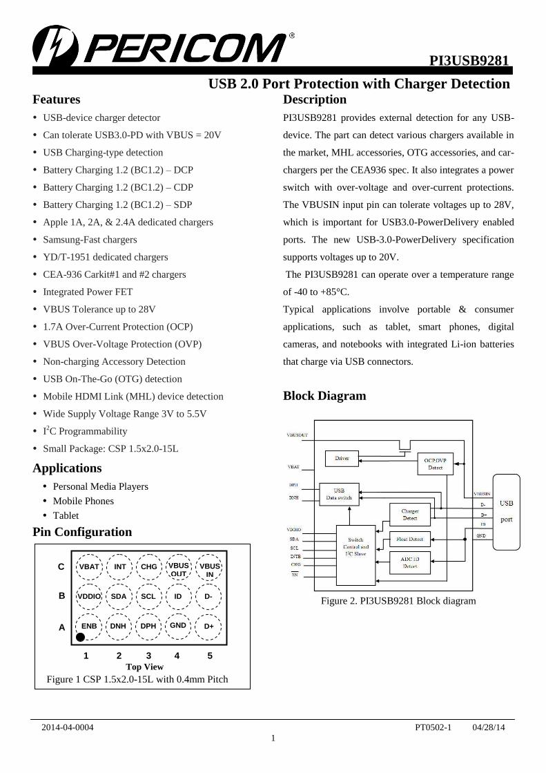
Block Diagram
Figure 2. PI3USB9281 Block diagram
A
B
C VBAT INT CHG VBUSOUT
VBUSIN
VDDIO SDA SCL ID D-
ENB DNH DPH GND D+
1 2 3 4 5
Top View
Figure 1 CSP 1.5x2.0-15L with 0.4mm Pitch
|||||||||||||||||||||||||||||||||||||||||||||||||||||||||||||||||||||||||||||||||||||||||||||||||||||||||||||||||||||||||||||||||||||||||||||||||||||||||||||||||||||||||||||||||||||||||||||||||||||||||||||||||||||||||||||||||||||||||||||||||||||||||||||||||||||||||||||||||||||||||||||||||||||||||||||||||||||||||||||||||||||||
2014-04-0004 PT0502-1 04/28/14
2
PI3USB9281
USB 2.0 Port Protection with Charger Detection
Pin Descriptions Name Type Default State Description
USB Interface
DPH Signal Path Open D+ signal switch path, dedicated USB port to be connected to the resident USB
transceiver on the device
DNH Signal Path Open D- signal switch path, dedicated USB port to be connected to the resident USB
transceiver on the device
Connector Interface
ID Signal Path Open Connected to the USB connector ID pin and used for detecting accessories
D+ Signal Path Open Connected to the USB connector D+ pin; depending on the signaling
mode
D- Signal Path Open Connected to the USB connector D- pin; depending on the signaling mode
VBUSIN Power Path NA Input voltage supply pin to be connected to the VBUS pin of the USB connector
Power Interface
VBAT Power NA Input voltage supply pin to be connected to the device battery output or to an
internal regulator
VDDIO Power NA Baseband processor interface I/O supply pin
ENB Input Hi-Z System enable for the circuit (Active Low)
GND Power NA Ground
Charger Interface
VBUSOUT Power Path NA Output voltage supply pin to be connected to the source voltage pin on the charger IC
CHG Open-Drain
Output Hi-Z
Open-drain active LOW output, used to signal the charger IC that a charger has been
attached
I2C Interface
SCL Input Hi-Z I2C serial clock signal to be connected to the phone-based I
2C master
SDA Open-Drain I/O Hi-Z I2C serial data signal to be connected to the phone-based I
2C master
INTB CMOS Output LOW Interrupt active LOW output used to prompt the phone baseband processor to read the I
2C
register bits, indicates a change in ID pin status or accessory attach status
Maximum Ratings
Storage Temperature ................................................................................... -65oC to +150oC
Supply Voltage from Battery/Baseband ..................................................... -0.5V to +6.5V
Supply Voltage from Micro-USB Connector ........................................ -0.5V to +28.0V
Switch I/O Voltage USB ................................................................................ -1.0V to +5.5V
Input Clamp Diode current.............................................................................................. 50mA
Charger Detect CHG Pin Sink current ......................................................................... 30mA
Switch I/O Current (Continuous) USB ....................................................................... 50mA
Switch I/O Switch Peak Current (Pulsed at 1ms Duration, <10% Duty Cycle)
USB, and All Other Channels ..................................................................................... 150mA
Charger FET............................................................................................................................. 2A
ESD: HBM ..................................................................................................................... 2000V
HB M (USB connector pins: VBUSIN, D+, D+, ID to GND) ................. 6000V
Recommended operation conditions
Symbol Parameter Min. Max. Units
VBAT Battery Supply Voltage 3.0 5.5 V
VBAT_TH Battery Supply Voltage Threshold - 3.0 V
VBUSIN VBUSIN Pin Supply Voltage 4.0 5.5 V
VDDIO Processor Supply Voltage 1.8 5.5 V
VSW Switch I/O Voltage USB Path Active 0 3.6 V
CID Capacitive Load on ID Pin for Reliable Accessory Detection 0 1.0 nF
TA Operating Temperature -40 85 °C
Note:
Stresses greater than those listed under MAXIMUM
RATINGS may cause permanent damage to the
device. This is a stress rating only and functional
operation of the device at these or any other
conditions above those indicated in the operational
sections of this specification is not implied.
Exposure to absolute maximum rating conditions
for extended periods may affect reliability.
|||||||||||||||||||||||||||||||||||||||||||||||||||||||||||||||||||||||||||||||||||||||||||||||||||||||||||||||||||||||||||||||||||||||||||||||||||||||||||||||||||||||||||||||||||||||||||||||||||||||||||||||||||||||||||||||||||||||||||||||||||||||||||||||||||||||||||||||||||||||||||||||||||||||||||||||||||||||||||||||||||||||
2014-04-0004 PT0502-1 04/28/14
3
PI3USB9281
USB 2.0 Port Protection with Charger Detection
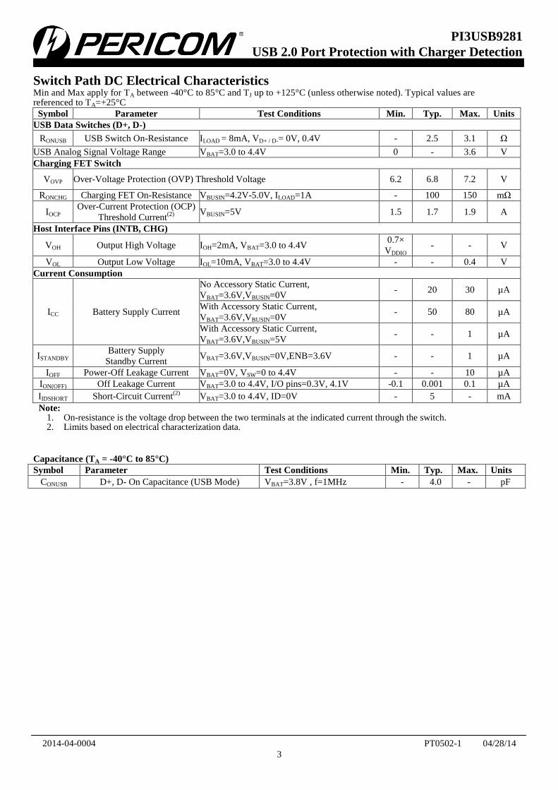
Switch Path DC Electrical Characteristics Min and Max apply for TA between -40°C to 85°C and TJ up to +125°C (unless otherwise noted). Typical values are referenced to TA=+25°C
Symbol Parameter Test Conditions Min. Typ. Max. Units
USB Data Switches (D+, D-)
RONUSB USB Switch On-Resistance ILOAD = 8mA, VD+ / D-= 0V, 0.4V - 2.5 3.1 Ω
USB Analog Signal Voltage Range VBAT=3.0 to 4.4V 0 - 3.6 V
Charging FET Switch
VOVP Over-Voltage Protection (OVP) Threshold Voltage 6.2 6.8 7.2 V
RONCHG Charging FET On-Resistance VBUSIN=4.2V-5.0V, ILOAD=1A - 100 150 mΩ
IOCP Over-Current Protection (OCP)
Threshold Current(2)
VBUSIN=5V 1.5 1.7 1.9 A
Host Interface Pins (INTB, CHG)
VOH Output High Voltage IOH=2mA, VBAT=3.0 to 4.4V 0.7×
VDDIO - - V
VOL Output Low Voltage IOL=10mA, VBAT=3.0 to 4.4V - - 0.4 V
Current Consumption
ICC Battery Supply Current
No Accessory Static Current,
VBAT=3.6V,VBUSIN=0V - 20 30 µA
With Accessory Static Current,
VBAT=3.6V,VBUSIN=0V - 50 80 µA
With Accessory Static Current,
VBAT=3.6V,VBUSIN=5V - - 1 µA
ISTANDBY Battery Supply
Standby Current VBAT=3.6V,VBUSIN=0V,ENB=3.6V - - 1 µA
IOFF Power-Off Leakage Current VBAT=0V, VSW=0 to 4.4V - - 10 µA
ION(OFF) Off Leakage Current VBAT=3.0 to 4.4V, I/O pins=0.3V, 4.1V -0.1 0.001 0.1 µA
IIDSHORT Short-Circuit Current(2)
VBAT=3.0 to 4.4V, ID=0V - 5 - mA
Note: 1. On-resistance is the voltage drop between the two terminals at the indicated current through the switch. 2. Limits based on electrical characterization data.
Capacitance (TA = -40°C to 85°C)
Symbol Parameter Test Conditions Min. Typ. Max. Units
CONUSB D+, D- On Capacitance (USB Mode) VBAT=3.8V , f=1MHz - 4.0 - pF
|||||||||||||||||||||||||||||||||||||||||||||||||||||||||||||||||||||||||||||||||||||||||||||||||||||||||||||||||||||||||||||||||||||||||||||||||||||||||||||||||||||||||||||||||||||||||||||||||||||||||||||||||||||||||||||||||||||||||||||||||||||||||||||||||||||||||||||||||||||||||||||||||||||||||||||||||||||||||||||||||||||||
2014-04-0004 PT0502-1 04/28/14
4
PI3USB9281
USB 2.0 Port Protection with Charger Detection
Switch AC Electrical Characteristics Min and Max apply for TA between -40°C to 85°C and TJ up to +125°C (unless otherwise noted). Typical values are referenced to TA=+25°C, VBAT=3.8V.
Symbol Parameter Test Conditions Min. Typ. Max. Units
BWUSB -3dB Bandwidth of USB channel - 1300 - MHz
OIRR OFF-Isolation USB Mode f=1MHz, RS=50Ω, CL=0 - -70 - dB
XTALK Active Channel
Crosstalk D+ to D- USB Mode
f=1MHz, RS=50Ω, CL=0 - -70 - dB
f=240MHz, RS=50Ω, CL=0 - -30 -
tSK(P) Skew of Opposite Transitions of the Same
Output (USB Mode)
tr=tf=750ps (10-90%) at
240MHz, CL=0pF, RL=50Ω - 30 - ps
tI2CRST Time When I
2C_SDA and I
2C_SCL Both
LOW to Cause a Reset - 15 - - ms
tINTMASK
Time after INT Mask Cleared to “0” until
INTB Goes LOW to Signal the Interrupt
after Interruptible Event while INT Mask
Bit Set to “1”
- 25 - - ms
tSDPDET
Time from VBUSIN Valid to VBUSOUT Valid
with Charger FET Closed and USB
Switches Closed for USB Standard
Downstream Port
See Figure 6 - 200 - ms
tCHGOUT
Time from VBUSIN Valid to VBUSOUT Valid
with Charger FET Closed for USB
Charging Ports(CDP and DCP)
See Figure 4 and Figure 5 - 200 - ms
tCARKIT Time from VBUSIN Valid to Car Kit Type 1
or Type 2 Charger Detected See Figure 8 - 130 - ms
tIDDET
Time from ID Not Floating to INTB LOW
to Signal Accessory Attached that is ID
Resistance-Based Only (VBUSIN Not Valid)
See Figure 9 - 100 - ms
I2C Controller DC Electrical Characteristics
Symbol Parameter Fast Mode (400kHz)
Units Min. Max.
VIL Low-Level Input Voltage -0.5 0.3VDDIO V
VIH High-Level Input Voltage 0.7VDDIO - V
VHYS Hysteresis of Schmitt Trigger Inputs VDDIO>2V 0.05VDDIO -
V VDDIO<2V 0.1VDDIO -
VOL1 Low-Level Output Voltage at 3mA Sink Current (Open-
Drain)
VDDIO>2V 0 0.4 V
VDDIO<2V - 0.2VDDIO
II2C Input Current of I2C SDA and SCL Pins, Input Voltage 0.26V to2.34V -10 10 µA
CI Capacitance for Each I/O Pin - 10 pF
I2C AC Electrical Characteristics
Symbol Parameter Fast Mode (400kHz)
Units Min. Max.
fSCL SCL Clock Frequency 0 400 kHz
tHDSTA Hold Time (Repeated) START Condition 0.6 - µs
tLOW LOW Period of SCL Clock 1.3 - µs
tHIGH HIGH Period of SCL Clock 0.6 - µs
tSETSTA Set-up Time for Repeated START Condition 0.6 - µs
tHDDAT Data Hold Time 0 0.9 µs
tSETDAT Data Set-up Time(1)
100 - ns
tr Rsie Time of SDA and SCL Signals(2)
20+0.1Cb 300 ns
tf Fall Time of SDA and SCL Signals(2)
20+0.1Cb 300
tSETSTO Set-up Time for STOP Condition 0.6 - µs
tBUF Bus-Free Time between STOP and START Conditions 1.3 - µs
tSP Pulse Width of Spikes that Must Be Suppressed by the Input Filter 0 50 ns
Notes:
1. A fast-mode I2C-bus device can be used in a standard-mode I
2C-bus system, but the requirement tSETDAT ≥ 250ns must be met.
|||||||||||||||||||||||||||||||||||||||||||||||||||||||||||||||||||||||||||||||||||||||||||||||||||||||||||||||||||||||||||||||||||||||||||||||||||||||||||||||||||||||||||||||||||||||||||||||||||||||||||||||||||||||||||||||||||||||||||||||||||||||||||||||||||||||||||||||||||||||||||||||||||||||||||||||||||||||||||||||||||||||
2014-04-0004 PT0502-1 04/28/14
5
PI3USB9281
USB 2.0 Port Protection with Charger Detection
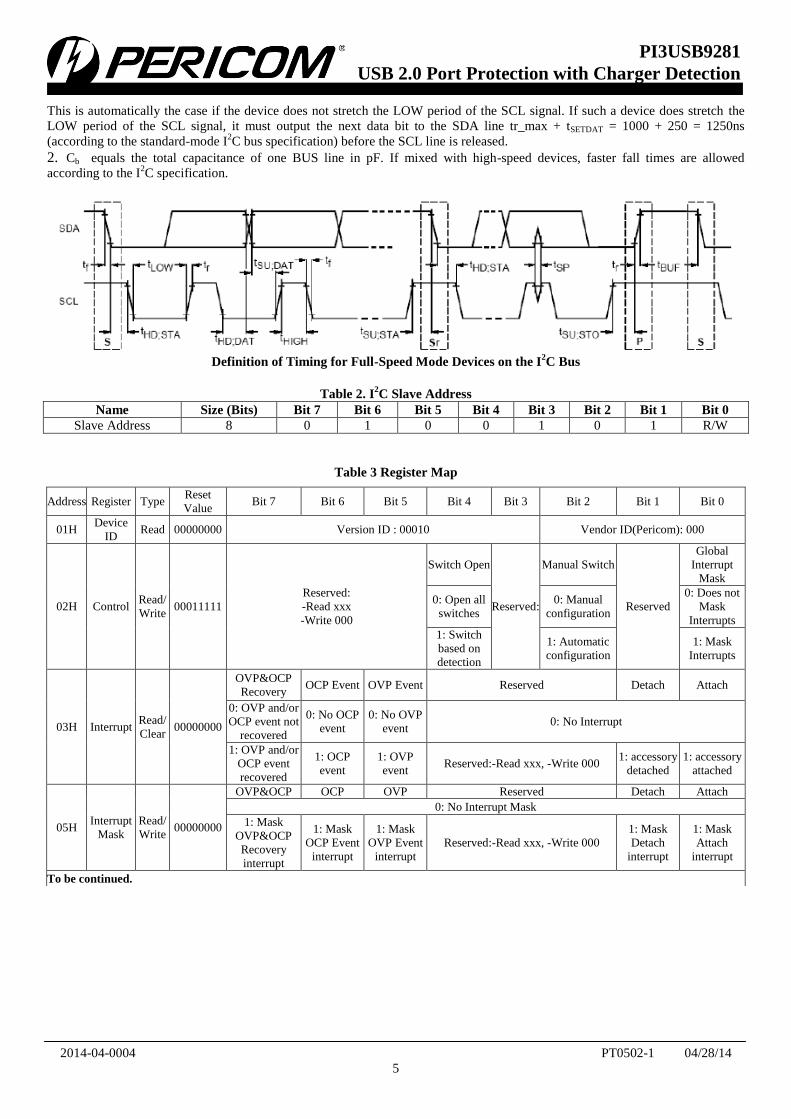
This is automatically the case if the device does not stretch the LOW period of the SCL signal. If such a device does stretch the
LOW period of the SCL signal, it must output the next data bit to the SDA line tr_max + tSETDAT = 1000 + 250 = 1250ns
(according to the standard-mode I2C bus specification) before the SCL line is released.
2. Cb equals the total capacitance of one BUS line in pF. If mixed with high-speed devices, faster fall times are allowed
according to the I2C specification.
Definition of Timing for Full-Speed Mode Devices on the I
2C Bus
Table 2. I
2C Slave Address
Name Size (Bits) Bit 7 Bit 6 Bit 5 Bit 4 Bit 3 Bit 2 Bit 1 Bit 0
Slave Address 8 0 1 0 0 1 0 1 R/W
Table 3 Register Map
Address Register Type Reset
Value Bit 7 Bit 6 Bit 5 Bit 4 Bit 3 Bit 2 Bit 1 Bit 0
01H Device
ID Read 00000000 Version ID : 00010 Vendor ID(Pericom): 000
02H Control Read/
Write 00011111
Reserved:
-Read xxx
-Write 000
Switch Open
Reserved:
Manual Switch
Reserved
Global
Interrupt
Mask
0: Open all
switches
0: Manual
configuration
0: Does not
Mask
Interrupts
1: Switch
based on
detection
1: Automatic
configuration
1: Mask
Interrupts
03H Interrupt Read/
Clear 00000000
OVP&OCP
Recovery OCP Event OVP Event Reserved Detach Attach
0: OVP and/or
OCP event not
recovered
0: No OCP
event
0: No OVP
event 0: No Interrupt
1: OVP and/or
OCP event
recovered
1: OCP
event
1: OVP
event Reserved:-Read xxx, -Write 000
1: accessory
detached
1: accessory
attached
05H Interrupt
Mask
Read/
Write 00000000
OVP&OCP OCP OVP Reserved Detach Attach
0: No Interrupt Mask
1: Mask
OVP&OCP
Recovery
interrupt
1: Mask
OCP Event
interrupt
1: Mask
OVP Event
interrupt
Reserved:-Read xxx, -Write 000
1: Mask
Detach
interrupt
1: Mask
Attach
interrupt
To be continued.
|||||||||||||||||||||||||||||||||||||||||||||||||||||||||||||||||||||||||||||||||||||||||||||||||||||||||||||||||||||||||||||||||||||||||||||||||||||||||||||||||||||||||||||||||||||||||||||||||||||||||||||||||||||||||||||||||||||||||||||||||||||||||||||||||||||||||||||||||||||||||||||||||||||||||||||||||||||||||||||||||||||||
2014-04-0004 PT0502-1 04/28/14
6
PI3USB9281
USB 2.0 Port Protection with Charger Detection
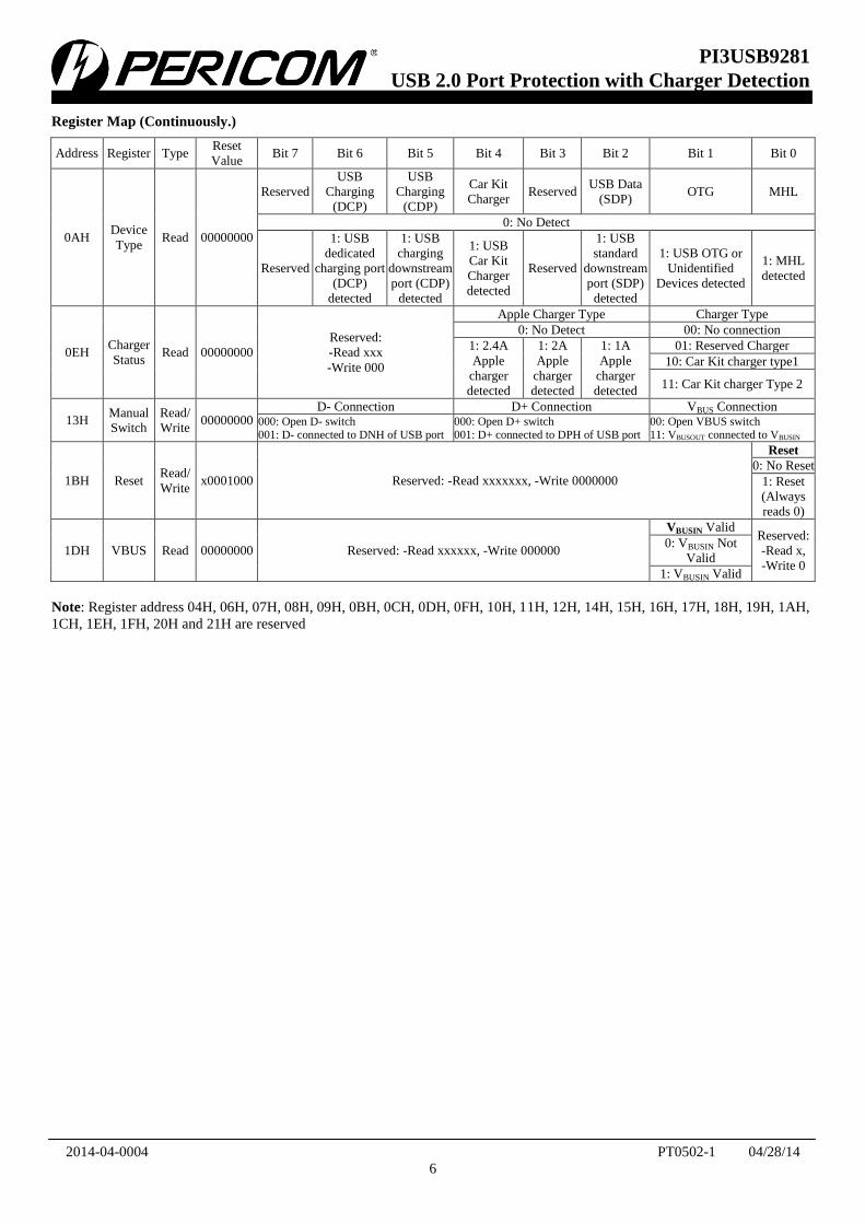
Register Map (Continuously.)
Note: Register address 04H, 06H, 07H, 08H, 09H, 0BH, 0CH, 0DH, 0FH, 10H, 11H, 12H, 14H, 15H, 16H, 17H, 18H, 19H, 1AH,
1CH, 1EH, 1FH, 20H and 21H are reserved
Address Register Type Reset
Value Bit 7 Bit 6 Bit 5 Bit 4 Bit 3 Bit 2 Bit 1 Bit 0
0AH Device
Type Read 00000000
Reserved
USB
Charging
(DCP)
USB
Charging
(CDP)
Car Kit
Charger Reserved
USB Data
(SDP) OTG MHL
0: No Detect
Reserved
1: USB
dedicated
charging port
(DCP)
detected
1: USB
charging
downstream
port (CDP)
detected
1: USB
Car Kit
Charger
detected
Reserved
1: USB
standard
downstream
port (SDP)
detected
1: USB OTG or
Unidentified
Devices detected
1: MHL
detected
0EH Charger
Status Read 00000000
Reserved:
-Read xxx
-Write 000
Apple Charger Type Charger Type
0: No Detect 00: No connection
1: 2.4A
Apple
charger
detected
1: 2A
Apple
charger
detected
1: 1A
Apple
charger
detected
01: Reserved Charger
10: Car Kit charger type1
11: Car Kit charger Type 2
13H Manual
Switch
Read/
Write 00000000
D- Connection D+ Connection VBUS Connection 000: Open D- switch 001: D- connected to DNH of USB port
000: Open D+ switch 001: D+ connected to DPH of USB port
00: Open VBUS switch 11: VBUSOUT connected to VBUSIN
1BH Reset Read/
Write x0001000 Reserved: -Read xxxxxxx, -Write 0000000
Reset
0: No Reset
1: Reset
(Always
reads 0)
1DH VBUS Read 00000000 Reserved: -Read xxxxxx, -Write 000000
VBUSIN Valid Reserved:
-Read x,
-Write 0
0: VBUSIN Not
Valid
1: VBUSIN Valid
|||||||||||||||||||||||||||||||||||||||||||||||||||||||||||||||||||||||||||||||||||||||||||||||||||||||||||||||||||||||||||||||||||||||||||||||||||||||||||||||||||||||||||||||||||||||||||||||||||||||||||||||||||||||||||||||||||||||||||||||||||||||||||||||||||||||||||||||||||||||||||||||||||||||||||||||||||||||||||||||||||||||
2014-04-0004 PT0502-1 04/28/14
7
PI3USB9281
USB 2.0 Port Protection with Charger Detection
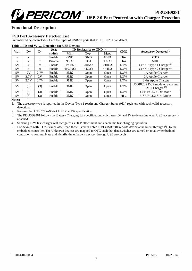
Functional Description
USB Port Accessory Detection List Summarized below in Table 1 are the types of USB2.0 ports that PI3USB9281 can detect.
Table 1. ID and VBUSIN Detection for USB Devices
VBUS D+ D- USB
switch
ID Resistance to GND (5)
CHG Accessory Detected
(1)
Min. Typ. Max.
x x x Enable GND GND GND Hi-z OTG
x x x Disable 950Ω 1kΩ 1.05Ω Hi-z MHL
5V x x Enable 190kΩ 200kΩ 210kΩ LOW Car Kit Type 1 Charger(2)
5V x x Enable 419.9kΩ 442kΩ 464kΩ LOW Car Kit Type 2 Charger(2)
5V 2V 2.7V Enable 3MΩ Open Open LOW 1A Apple Charger
5V 2.7V 2V Enable 3MΩ Open Open LOW 2A Apple Charger
5V 2.7V 2.7V Enable 3MΩ Open Open LOW 2.4A Apple Charger
5V (3) (3) Enable 3MΩ Open Open LOW USBBC1.2 DCP mode or Samsung
FAST Charger (4)
5V (3) (3) Enable 3MΩ Open Open LOW USB BC1.2 CDP Mode
5V (3) (3) Enable 3MΩ Open Open Hi-z USB BC1.2 SDP Mode
Notes:
1. The accessory type is reported in the Device Type 1 (0Ah) and Charger Status (0Eh) registers with each valid accessory
detection.
2. Follows the ANSI/CEA-936-A USB Car Kit specification.
3. The PI3USB9281 follows the Battery Charging 1.2 specification, which uses D+ and D- to determine what USB accessory is
attached.
4. Samsung 1.2V fast charger will recognize as DCP attachment and enable the fast charging operation.
5. For devices with ID resistance other than those listed in Table 1, PI3USB9281 reports device attachment through I2C to the
embedded controller. The Unknown devices are mapped to OTG such that data switches are turned on to allow embedded
controller to communicate and identify the unknown devices through USB protocols.
|||||||||||||||||||||||||||||||||||||||||||||||||||||||||||||||||||||||||||||||||||||||||||||||||||||||||||||||||||||||||||||||||||||||||||||||||||||||||||||||||||||||||||||||||||||||||||||||||||||||||||||||||||||||||||||||||||||||||||||||||||||||||||||||||||||||||||||||||||||||||||||||||||||||||||||||||||||||||||||||||||||||
2014-04-0004 PT0502-1 04/28/14
8
PI3USB9281
USB 2.0 Port Protection with Charger Detection
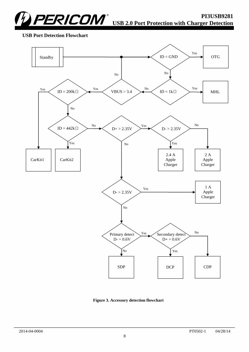
USB Port Detection Flowchart
Figure 3. Accessory detection flowchart
Standby
VBUS > 3.4 ID = 200kΩ
CarKit1
ID = 442kΩ
CarKit2
D+ > 2.35V D- > 2.35V
2.4 A
Apple
Charger
Yes Yes
Yes
Yes
Yes
No No
No
No
Primary detect
D- = 0.6V
SDP
Secondary detect
D+ = 0.6V
DCP CDP
Yes
Yes
No
No
2 A
Apple
Charger
D- > 2.35V
1 A
Apple
Charger
Yes
No
No
ID = 1kΩ MHL
OTG ID = GND
No
No
Yes
Yes
|||||||||||||||||||||||||||||||||||||||||||||||||||||||||||||||||||||||||||||||||||||||||||||||||||||||||||||||||||||||||||||||||||||||||||||||||||||||||||||||||||||||||||||||||||||||||||||||||||||||||||||||||||||||||||||||||||||||||||||||||||||||||||||||||||||||||||||||||||||||||||||||||||||||||||||||||||||||||||||||||||||||
2014-04-0004 PT0502-1 04/28/14
9
PI3USB9281
USB 2.0 Port Protection with Charger Detection
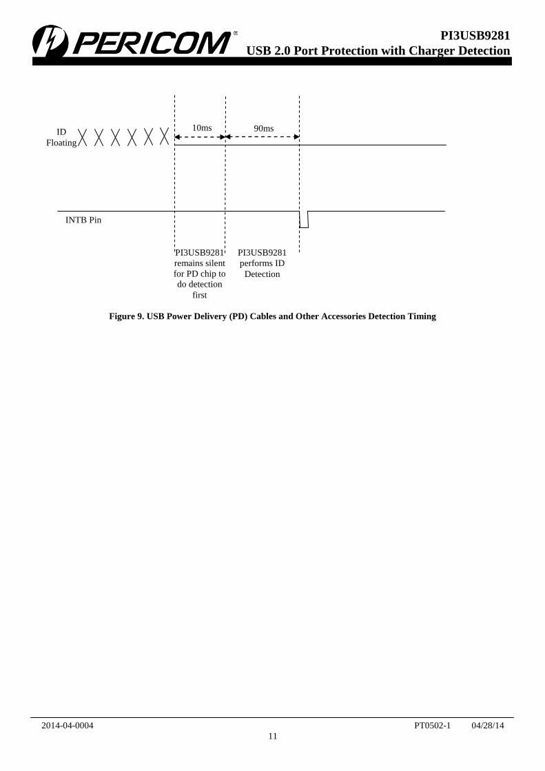
USB Port Detection Timing The following figures show the attach timing of the USB after insertion of accessories and the relationship between the INTB
assertion and the CHG assertion. PI3USB9281 has incorporated a VBUS de-bounce circuit that waits a settle time of the USB cable.
Figure 4. USB Charging Downstream Port (CDP) Attach Timing
Figure 5. USB Dedicated Charging Port (DCP) Attach Timing
VBUSIN>4.0V Charger FET closed, INTB
asserted and registers written
INTB Pin
CHG Pin 50ms
VBUSIN Voltage
VBUSOUT 200ms
ID Floating
USB switch Open Closed
200ms
VBUSIN>4.0V Charger FET closed, INTB
asserted and registers written
INTB Pin
CHG Pin 50ms
VBUSIN Voltage
VBUSOUT VBUSIN Valid 130mS
250ms CHG detection 70ms
ID Floating
USB switch Open Closed
200ms
|||||||||||||||||||||||||||||||||||||||||||||||||||||||||||||||||||||||||||||||||||||||||||||||||||||||||||||||||||||||||||||||||||||||||||||||||||||||||||||||||||||||||||||||||||||||||||||||||||||||||||||||||||||||||||||||||||||||||||||||||||||||||||||||||||||||||||||||||||||||||||||||||||||||||||||||||||||||||||||||||||||||
2014-04-0004 PT0502-1 04/28/14
10
PI3USB9281
USB 2.0 Port Protection with Charger Detection
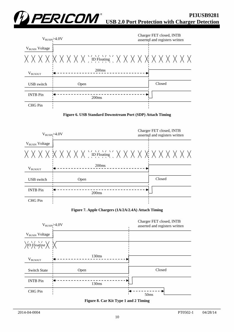
Figure 6. USB Standard Downstream Port (SDP) Attach Timing
Figure 7. Apple Chargers (1A/2A/2.4A) Attach Timing
Figure 8. Car Kit Type 1 and 2 Timing
VBUSIN>4.0V Charger FET closed, INTB
asserted and registers written
INTB Pin
CHG Pin
VBUSIN Voltage
VBUSOUT 200ms
ID Floating
USB switch Open Closed
200ms
VBUSIN>4.0V Charger FET closed, INTB
asserted and registers written
INTB Pin
CHG Pin 50ms
VBUSIN Voltage
VBUSOUT 130ms
ID Floating
Switch State Open Closed
130ms
VBUSIN>4.0V Charger FET closed, INTB
asserted and registers written
INTB Pin
CHG Pin
VBUSIN Voltage
VBUSOUT 200ms
ID Floating
USB switch Open Closed
200ms
|||||||||||||||||||||||||||||||||||||||||||||||||||||||||||||||||||||||||||||||||||||||||||||||||||||||||||||||||||||||||||||||||||||||||||||||||||||||||||||||||||||||||||||||||||||||||||||||||||||||||||||||||||||||||||||||||||||||||||||||||||||||||||||||||||||||||||||||||||||||||||||||||||||||||||||||||||||||||||||||||||||||
2014-04-0004 PT0502-1 04/28/14
11
PI3USB9281
USB 2.0 Port Protection with Charger Detection
Figure 9. USB Power Delivery (PD) Cables and Other Accessories Detection Timing
INTB Pin
ID
Floating
10ms
PI3USB9281
remains silent
for PD chip to
do detection
first
90ms
PI3USB9281
performs ID
Detection
|||||||||||||||||||||||||||||||||||||||||||||||||||||||||||||||||||||||||||||||||||||||||||||||||||||||||||||||||||||||||||||||||||||||||||||||||||||||||||||||||||||||||||||||||||||||||||||||||||||||||||||||||||||||||||||||||||||||||||||||||||||||||||||||||||||||||||||||||||||||||||||||||||||||||||||||||||||||||||||||||||||||
2014-04-0004 PT0502-1 04/28/14
12
PI3USB9281
USB 2.0 Port Protection with Charger Detection
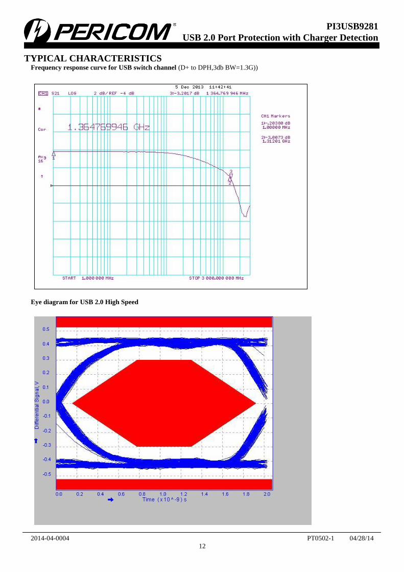
TYPICAL CHARACTERISTICS
Frequency response curve for USB switch channel (D+ to DPH,3db BW=1.3G))
Eye diagram for USB 2.0 High Speed
|||||||||||||||||||||||||||||||||||||||||||||||||||||||||||||||||||||||||||||||||||||||||||||||||||||||||||||||||||||||||||||||||||||||||||||||||||||||||||||||||||||||||||||||||||||||||||||||||||||||||||||||||||||||||||||||||||||||||||||||||||||||||||||||||||||||||||||||||||||||||||||||||||||||||||||||||||||||||||||||||||||||
2014-04-0004 PT0502-1 04/28/14
13
PI3USB9281
USB 2.0 Port Protection with Charger Detection
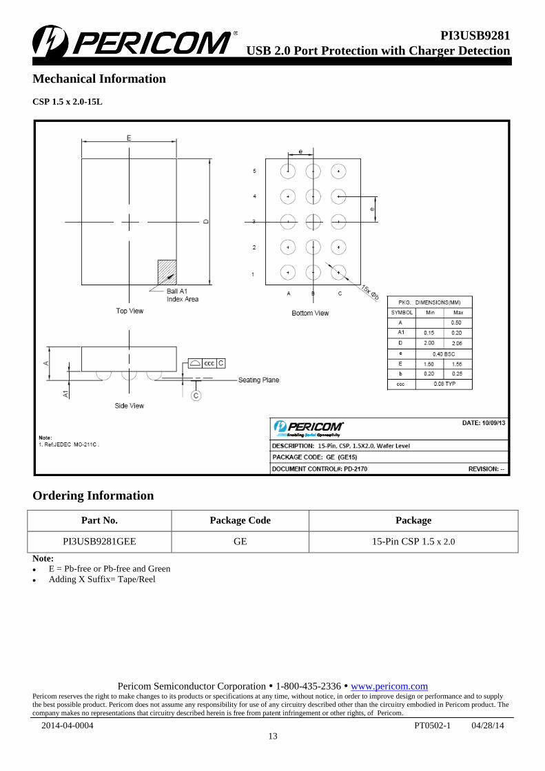
Mechanical Information
CSP 1.5 x 2.0-15L
Ordering Information
Part No. Package Code Package
PI3USB9281GEE GE 15-Pin CSP 1.5 x 2.0
Note:
E = Pb-free or Pb-free and Green
Adding X Suffix= Tape/Reel
Pericom Semiconductor Corporation 1-800-435-2336 www.pericom.com Pericom reserves the right to make changes to its products or specifications at any time, without notice, in order to improve design or performance and to supply the best possible product. Pericom does not assume any responsibility for use of any circuitry described other than the circuitry embodied in Pericom product. The
company makes no representations that circuitry described herein is free from patent infringement or other rights, of Pericom.