Embed Size (px)
Citation preview

TechTools • PIC Mini Data Sheets • Page 1
PIC Mini Data Sheets
DS
ContentsPIC16C5x........................................................... 5PIC16C5x Pin-Outs ......................................................................... 5PIC16C5x Microcontrollers ............................................................ 6Peripheral Features ........................................................................ 6Internal Architecture....................................................................... 9PIC16C5x Registers ........................................................................ 9
PIC16C64......................................................... 18PIC16C64 Pin-Out ..........................................................................18New and Modified Features ..........................................................19PIC16C64 Registers .......................................................................21PIC16C64 Register Description ....................................................24
PIC16C71......................................................... 41PIC16C71 Pin-Out ..........................................................................41PIC16C71 Microcontrollers ...........................................................42New and Modified Features ..........................................................42PIC16C71 Registers .......................................................................44
PIC16C84......................................................... 54PIC16C84 Pin-Out ..........................................................................54PIC16C84 Microcontrollers ...........................................................55New and Modified Features ..........................................................55PIC16C84 Registers .......................................................................57Reading & Writing EEPROM Registers ........................................66

Page 2 • PIC Mini Data Sheets • TechTools
PIC Mini Data Sheets

TechTools • PIC Mini Data Sheets • Page 3
PIC Mini Data Sheets
DS
This appendix contains “mini data sheets” for the PIC16C5x, 16C64,16C71, and 16C84. These mini data sheets include commonly usedinformation, such as pin-out’s, memory maps, bit functions, etc. Alsoincluded are helpful software tips and design suggestions. For mosteveryday needs, we hope you’ll find these mini data sheets useful. If youneed more detailed information, such as timing and temperaturecharacteristics, please refer to the Microchip data sheets.

Page 4 • PIC Mini Data Sheets • TechTools
PIC Mini Data Sheets

TechTools • PIC Mini Data Sheets • Page 5
PIC Mini Data Sheets
DS
PIC16C5x Pin-OutsThe following diagrams show the 18-pin and 28-pin PIC16C5x pin-outs:
Pin Function
RA0 - RA3 I/O Port ARB0 - RB7 I/O Port BRC0 - RC7 I/O Port C (only on 28-pin PIC’s)RTCC Real-time clock/counter inputMCLR Master clear (reset)OSC1 Oscillator inputOSC2/CLKOUT Oscillator output (OSC/4)Vdd Power supplyVss GroundN/C No connection
RA2
RA3
RTCC
MCLR
Vss
RB0
RB1
RB2
RB3
RA1
RA0
OSC1
OSC2/CLKOUT
Vdd
RB7
RB6
RB5
RB4
1
2
3
4
5
6
7
8
9
18
17
16
15
14
13
12
11
10
PIC16C54, -56, -58
PDIPCERDIP
SOIC
RTCC
Vdd
N/C
Vss
N/C
RA0
RA1
RA2
RA3
RB0
RB1
RB2
RB3
RB4
MCLR
OSC1
OSC2/CLKOUT
RC7
RC6
RC5
RC4
RC3
RC2
RC1
RC0
RB7
RB6
RB5
1
2
3
4
5
6
7
8
9
10
11
12
13
14
28
27
26
25
24
23
22
21
20
19
18
17
16
15
PDIPCERDIP
SOIC
PIC16C55, -57
PIC16C5x
Page 6 • PIC Mini Data Sheets • TechTools
PIC Mini Data Sheets
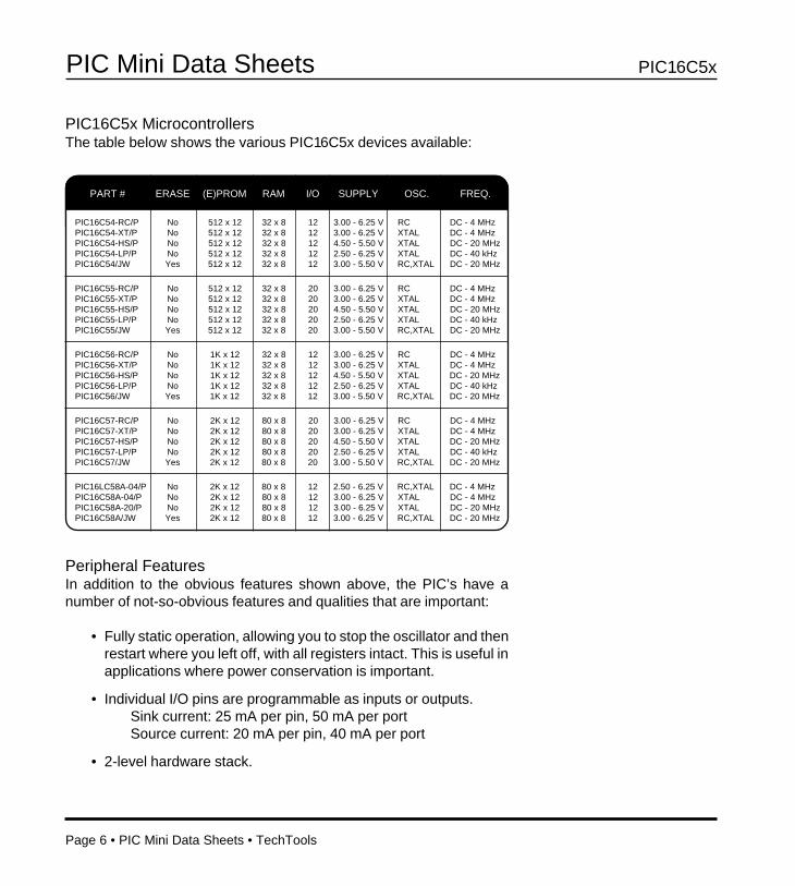
PIC16C5x MicrocontrollersThe table below shows the various PIC16C5x devices available:
PART # ERASE (E)PROM RAM I/O SUPPLY OSC. FREQ.
PIC16C54-RC/P No 512 x 12 32 x 8 12 3.00 - 6.25 V RC DC - 4 MHzPIC16C54-XT/P No 512 x 12 32 x 8 12 3.00 - 6.25 V XTAL DC - 4 MHzPIC16C54-HS/P No 512 x 12 32 x 8 12 4.50 - 5.50 V XTAL DC - 20 MHzPIC16C54-LP/P No 512 x 12 32 x 8 12 2.50 - 6.25 V XTAL DC - 40 kHzPIC16C54/JW Yes 512 x 12 32 x 8 12 3.00 - 5.50 V RC,XTAL DC - 20 MHz
PIC16C55-RC/P No 512 x 12 32 x 8 20 3.00 - 6.25 V RC DC - 4 MHzPIC16C55-XT/P No 512 x 12 32 x 8 20 3.00 - 6.25 V XTAL DC - 4 MHzPIC16C55-HS/P No 512 x 12 32 x 8 20 4.50 - 5.50 V XTAL DC - 20 MHzPIC16C55-LP/P No 512 x 12 32 x 8 20 2.50 - 6.25 V XTAL DC - 40 kHzPIC16C55/JW Yes 512 x 12 32 x 8 20 3.00 - 5.50 V RC,XTAL DC - 20 MHz
PIC16C56-RC/P No 1K x 12 32 x 8 12 3.00 - 6.25 V RC DC - 4 MHzPIC16C56-XT/P No 1K x 12 32 x 8 12 3.00 - 6.25 V XTAL DC - 4 MHzPIC16C56-HS/P No 1K x 12 32 x 8 12 4.50 - 5.50 V XTAL DC - 20 MHzPIC16C56-LP/P No 1K x 12 32 x 8 12 2.50 - 6.25 V XTAL DC - 40 kHzPIC16C56/JW Yes 1K x 12 32 x 8 12 3.00 - 5.50 V RC,XTAL DC - 20 MHz
PIC16C57-RC/P No 2K x 12 80 x 8 20 3.00 - 6.25 V RC DC - 4 MHzPIC16C57-XT/P No 2K x 12 80 x 8 20 3.00 - 6.25 V XTAL DC - 4 MHzPIC16C57-HS/P No 2K x 12 80 x 8 20 4.50 - 5.50 V XTAL DC - 20 MHzPIC16C57-LP/P No 2K x 12 80 x 8 20 2.50 - 6.25 V XTAL DC - 40 kHzPIC16C57/JW Yes 2K x 12 80 x 8 20 3.00 - 5.50 V RC,XTAL DC - 20 MHz
PIC16LC58A-04/P No 2K x 12 80 x 8 12 2.50 - 6.25 V RC,XTAL DC - 4 MHzPIC16C58A-04/P No 2K x 12 80 x 8 12 3.00 - 6.25 V XTAL DC - 4 MHzPIC16C58A-20/P No 2K x 12 80 x 8 12 3.00 - 6.25 V XTAL DC - 20 MHzPIC16C58A/JW Yes 2K x 12 80 x 8 12 3.00 - 6.25 V RC,XTAL DC - 20 MHz
Peripheral FeaturesIn addition to the obvious features shown above, the PIC’s have anumber of not-so-obvious features and qualities that are important:
• Fully static operation, allowing you to stop the oscillator and thenrestart where you left off, with all registers intact. This is useful inapplications where power conservation is important.
• Individual I/O pins are programmable as inputs or outputs.Sink current: 25 mA per pin, 50 mA per portSource current: 20 mA per pin, 40 mA per port
• 2-level hardware stack.
PIC16C5x

TechTools • PIC Mini Data Sheets • Page 7
PIC Mini Data Sheets
DS
• Real-Time Clock/Counter (RTCC). The RTCC is an 8-bit counter,which can be driven by the RTCC pin or by the PIC’s internalinstruction clock (OSC/4). If the external pin is used, the countercan be set to increment on low-to-high or high-to-low transitions.
Normally, the RTCC is driven directly by either source. For highercount values, though, the prescaler can be used to effectivelyincrease the RTCC to 16 bits.
The RTCC signal source and trigger edge are determined by bitsin the Option register (see next section for register descriptions).
See the Microchip PIC16C5x data sheet for details concerningtiming characteristics for the RTCC’s external input.
• Watchdog Timer (WDT). When enabled, the watchdog timer isused to reset the PIC if the program has “crashed.” Normally, aCLR WDT instruction in the main loop of your program wouldprevent the watchdog timer from ever timing out and resetting thePIC. However, if the program was not executing properly, thewatchdog timer would reset the PIC.
The watchdog timer works from an internal oscillator, allowing it torun even if the PIC’s main oscillator has stopped. The watchdogtimer’s normal time-out period is 18 ms, but can be increased toseveral seconds by using the post-scaler.
• Prescaler/Post-scaler. This 8-bit counter can be assigned to theRTCC (as a prescaler) or the watchdog timer (as a post-scaler).For simplicity, this counter is normally referred to as the “prescaler,”even when it’s used as a post-scaler.
When assigned to the RTCC, the prescaler is placed between theRTCC and its clock source. The clock signal which would normallyincrement the RTCC, increments the prescaler. When the prescaleroverflows, the RTCC is incremented. Increment ratios from 1:2 -1:256 can be used, effectively giving you a 16-bit RTCC.
When assigned to the watchdog timer, the prescaler is placedbetween the watchdog timer and the PIC’s reset circuit. Thewatchdog timer signal which would normally reset the PIC,
PIC16C5x

Page 8 • PIC Mini Data Sheets • TechTools
PIC Mini Data Sheets
increments the prescaler. When the prescaler overflows, the PICis reset. Delay ratios from 1:1 - 1:128 can be used, allowing thewatchdog period to be set from 18 ms to several seconds.
The prescaler setup is determined by bits in the Option register(see the next section for register descriptions).
• Code-protect fuse. This is a special fuse that can be blown duringprogramming; once the fuse is blown, the PIC’s EPROM cannotbe read.
• Power saving sleep mode. For applications where low powerconsumption is important, the PIC has a sleep mode. This modeis entered by executing a SLEEP instruction, which shuts downthe oscillator. I/O pins maintain whatever state they had when thesleep mode was entered.
To awaken the PIC from sleep mode, a reset must be performed,either from the MCLR pin or from a watchdog timer time-out.
Once the PIC is running, the “PD” and “TO” bits in the Statusregister can be read to determine 1) if the PIC was powered up orawakened from sleep, and 2) if the wake-up was caused by anexternal reset or by the watchdog timer.
• Programmable oscillator type. The PIC can run with any of fouroscillator types, as shown below:
LP: Low power crystal (DC - 40 KHz)
RC: Resistor & capacitor (DC - 4 MHz, ± 13-39 percent)
XT: Crystal or resonator (100 KHz - 4 MHz)
HS: High speed crystal (4 - 20 MHz)
The oscillator type is determined by two EPROM bits, which arenormally programmed at the factory. The RC and erasable PIC’s,however, can be user-programmed for any of the oscillator types.Keep in mind, though, that RC-type PIC’s are only tested for usewith RC oscillators.
PIC16C5x

TechTools • PIC Mini Data Sheets • Page 9
PIC Mini Data Sheets
DS
Internal ArchitectureInternally, the PIC is based on a register file concept with separatebusses and memories for data and instructions (sometimes called“Harvard architecture”). The data bus and memory (RAM) are 8-bitswide, while the program bus and memory (EPROM) are 12-bits wide. AllPIC instructions and their operands fit into a single 12-bit word, resultingin smaller code and faster execution. PIC programs are typically 33-50percent smaller than programs written for 8-bit processors. And mostinstructions execute in a single instruction cycle (4 clock cycles);instructions that affect the program counter take an extra instructioncycle, for a total of 8 clock cycles. To further increase speed, the PICuses overlapping instruction fetch and execution cycles; while oneinstruction is executed, the following instruction is being read fromprogram memory. Because of its efficiency, the PIC can deliver 5 MIPSexecution with a clock frequency of 20 MHz.
PIC16C5x RegistersThe following table shows the various PIC16C5x registers; the functionof each register is described in the following pages.
Register Function
00h Indirect addressing register01h Real-time clock/counter (RTCC)02h Program counter (PC)- Stack registers (2)03h Status register04h File select register (FSR)05h I/O Port A06h I/O Port B07h I/O Port C- TRISA- TRISB- TRISC- W register- Option register08h - 0Fh General purpose registers10h - 1Fh General purpose registers (4 banks in PIC16C57)
PIC16C5x

Page 10 • PIC Mini Data Sheets • TechTools
PIC Mini Data Sheets
BANK 0
W register
Stack (2)
Option register
TRISA
TRISB
TRISC
Indirect addr.
RTCC
PC
STATUS
FSR
PORT A
PORT B
PORT C
8
general
purpose
registers
(RAM)
16
general
purpose
registers
(RAM)
(00h - 1Fh)
BANK 1*
W register
Stack (2)
Option register
TRISA
TRISB
TRISC
Indirect addr.
RTCC
PC
STATUS
FSR
PORT A
PORT B
PORT C
reads/writes
registers
08h - 0Fh
16
general
purpose
registers
(RAM)*
(20h - 3Fh)*
00h
01h
02h
03h
04h
05h
06h
07h
08h
0Fh
10h
1Fh
BANK 2*
W register
Stack (2)
Option register
TRISA
TRISB
TRISC
Indirect addr.
RTCC
PC
STATUS
FSR
PORT A
PORT B
PORT C
reads/writes
registers
08h - 0Fh
16
general
purpose
registers
(RAM)*
(40h - 5Fh)*
BANK 3*
W register
Stack (2)
Option register
TRISA
TRISB
TRISC
Indirect addr.
RTCC
PC
STATUS
FSR
PORT A
PORT B
PORT C
reads/writes
registers
08h - 0Fh
16
general
purpose
registers
(RAM)*
(60h - 7Fh)*
30h
3Fh
50h
5Fh
70h
7Fh
* Available on PIC16C57 only.
PIC16C5x

TechTools • PIC Mini Data Sheets • Page 11
PIC Mini Data Sheets
DS
The following text describes the function of each register. For some ofthe registers, you’ll notice the designation “xxh” following the registername. This indicates the address of the register. Registers with noaddress cannot be addressed directly.
• Indirect Addressing Register (00h). This register doesn’t actuallyexist. Naming register 00h in an instruction causes the PIC to readthe register pointed to by register 04h (file select register). Forexample, the instruction “ADD 00h,#05 ” will not add five toregister 00h; instead, it will add five to whatever register is pointedto by the address in register 04h.
If register 00h itself is read through register 04h (04h contains“00h”), 00h will be returned. If register 00h is written to throughregister 04h, the PIC will execute a NOP.
• Real-Time Clock/Counter (01h: RTCC). This is the location of theRTCC (see previous section for a description). Although itscontents may change in response to a clock signal, the RTCCregister may be read and written just as any other register.
• Program Counter (02h: PC). The program counter holds theaddress for the instruction currently being executed. The programcounter and its associated two-level stack are 9-11 bits wide,depending on the EPROM size of the PIC being used.
Certain instructions affect the program counter, as shown below:
GOTO (Microchip) and JMP (Parallax) load the lower 9 bits ofthe program counter. In the PIC16C56 and ’57, which havemore than 512 words of EPROM, the upper two bits of theprogram counter are loaded with the page select bits from thestatus register. The Parallax instruction set includes a conve-nient instruction, LJMP , which sets the page select bits beforeexecuting the jump.
CALL loads the lower 8 bits of the program counter and clearsthe ninth bit. The program counter + 1 is pushed into the stack.In the ’56 and ’57, the upper two bits of the program counterare loaded with the page select bits from the status register.The Parallax instruction set includes LCALL , which sets thepage select bits before executing the jump.
PIC16C5x
Page 12 • PIC Mini Data Sheets • TechTools
PIC Mini Data Sheets
RETLW (Microchip) and RETW (Parallax) load the programcounter with the address most recently pushed on the stackby a CALL instruction.
Instructions which load a computed value into the programcounter, such as JMP PC+W, load the value into the lower 8bits. The ninth bit of the program counter is cleared. In thePIC16C56 and ’57, the upper two bits of the program counterare loaded with the page select bits from the status register.
It should be noted that because the ninth bit of the program counteris cleared by CALL instructions and computed value instructions(such as JMP PC+W), all subroutine calls and computed jumpsmust have their destination in the first 256 locations of any page(each page is 512 words).
As you may have noticed when reading the JMP and CALLparagraphs above, the program counter may not be loaded asexpected when using a PIC with more than 512 words of EPROM.This is because the upper two bits of the program counter areloaded with the page select bits from the status register. If yourprogram continues into the second page of memory and executesa JMP without having properly set the page select bits, executionmay jump to another page (probably not what you want). To avoidthis mistake, make sure to set the page select bits for the correctpage. Or, use the Parallax “long” instructions, which do this for you(long instructions are LCALL, LJMP, and LSET).
• Stack. The stack is a pair of registers which are used for calling andreturning from subroutines. The stack is affected by two instruc-tions:
When a CALL is executed, the first stack register is copiedinto the second register, then the program counter + 1 (thereturn address) is loaded into the first register. The originalcontents of the second register are lost. Finally, the programcounter is loaded with the subroutine address, at which pointexecution continues.
PIC16C5x

TechTools • PIC Mini Data Sheets • Page 13
PIC Mini Data Sheets
DS
When a RETLW (Microchip) or RETW (Parallax) is executed,the first stack register is copied into the program counter, thenthe second register is copied into the first register. Executioncontinues at the address loaded from the first stack register.
• Status Register (03h). This register contains the status of thePIC’s arithmetic logic unit (ALU), the reset status, and the pageselect bits for PIC’s with more than 512 words of EPROM.
The function of each bit in the status register is shown below:
Bit Function
0 Carry bit (C). Set if an addition or subtraction causesan overflow from the most significant bit of the result-ant (bit 7). Subtraction is included because it’s ex-ecuted by adding the two’s complement.
Also used by rotate instructions, which rotate thecontents of a register and copy the low or high orderbit of the register into the carry bit.
1 Digit carry bit (DC). Set if an addition or subtractioncauses an overflow from the 4th low order bit (bit 3).Digit carry indicates that more than one hex digit (4bits) was necessary to accomodate the result.
2 Zero bit (Z). Set if the result of an arithmetic or logicoperation is zero.
3 Power-down bit (PD). Set during power-up or by aCLR WDT (clear watchdog) instruction. Cleared by aSLEEP instruction.
4 Time-out bit (TO). Set during power-up, by CLRWDT, or by SLEEP. Cleared by a watchdog time-out.
5-6 Page select bits (PA0, PA1). In the ’54 and ’55, theseare unused. In the ’56, bit 5 selects program page 0or 1 (bit 6 is unused). In the ’57, both bits select page0, 1, 2, or 3. Each page is 512 words long.
PIC16C5x

Page 14 • PIC Mini Data Sheets • TechTools
PIC Mini Data Sheets
Bit Function
7 Unused bit (PA2). Reserved by Microchip for futureuse.
The following table shows how various events affect thepower-down and time-out bits:
Event PD TO
Power-up 1 1Watchdog time-out x 0SLEEP instruction 0 1CLR WDT instruction 1 1
Lastly, this table shows the status of the power-down andtime-out bits after a reset:
Cause of Reset PD TO
Watchdog time-out (not during sleep) 1 0Watchdog time-out (during sleep) 0 0External reset (not during sleep) x xExternal reset (during sleep) 0 1Normal power-up 1 1
• File Select Register (04h: FSR). This register serves a dualpurpose: it selects the register for indirect addressing, and itselects the current register bank in the PIC16C57.
In all PIC16C5x devices, bits 0-4 select one of 32 registers in thecurrent bank (only the ’57 has more than one bank).
In the PIC16C57, bits 5-6 select one of four register banks. Eachbank has 32 registers. However, reading or writing the lower 16registers in any bank will access registers 00h - 0Fh (bank 0). Onlythe upper 16 registers in each bank are unique. This results in onebank of 32 registers, plus three banks of 16 registers, for a total of80 registers.
PIC16C5x

TechTools • PIC Mini Data Sheets • Page 15
PIC Mini Data Sheets
DS
The following table shows the function of each FSR bit:
Bit Function
0-4 Available in all PIC’s; select one of 32 registers in thecurrent bank (only the ’57 has more than 1 bank).
5-6 PIC16C57 only; select one of four register banks.
7 Read-only bit; always reads as “1”.
This table shows the registers available in the various PIC’s:
Registers Description
00h - 07h Special registers, bank 0 (RTCC, PC, etc.)
08h - 0Fh General purpose registers, bank 0
10h - 1Fh General purpose registers, upper half of bank 0
End of register memory in ’54, ’55, and ’56.
20h - 2Fh Reads/writes registers 00h - 0Fh
30h - 3Fh General purpose registers, upper half of bank 1
40h - 4Fh Reads/writes registers 00h - 0Fh
50h - 5Fh General purpose registers, upper half of bank 2
60h - 6Fh Reads/writes registers 00h - 0Fh
70h - 7Fh General purpose registers, upper half of bank 3
The register selected in the FSR can be accessed in the indirectaddressing mode (see description of indirect addressing register,earlier in this section).
In the PIC16C57, all registers can be accessed through indirectaddressing. However, to access registers above 1Fh using directinstructions, you must set the page select bits (5-6) to theappropriate page, then read or write the corresponding register in
PIC16C5x

Page 16 • PIC Mini Data Sheets • TechTools
PIC Mini Data Sheets
bank 0. For instance, to load register 30h with #A5h, you wouldexecute the following instructions:
MOV 04h,#00100000b ;Select bank 1
MOV 10h,#A5h ;Load register 10h in;bank 1 (register 30h);with #A5h
• I/O Port A (05h: RA or Port A). 4-bit I/O port. This register is usedto read and write I/O Port A. This register can be read and writtenjust as any other register. However, read instructions always readthe I/O pins, regardless of whether the pins are programmed asinputs or outputs.
The upper 4 bits are unused and read as 0’s.
• I/O Port B (06h: RB or Port B). 8-bit I/O port.
• I/O Port C (07h: RC or Port C). 8-bit I/O port, only available on 28-pin PIC’s. On 18-pin PIC’s, this register can be used for storage.
• TRISA (TRI-State A). This is the data direction register for Port A.Bits in this register which are set to “1” cause the correspondingbits in Port A to become inputs (the pins go into high impendencemode, allowing them to be driven by an external source). Bitswhich are cleared to “0” cause the corresponding bits in Port A tobecome outputs.
The data direction registers are not directly addressable; tochange their contents, you can use either of these instructions:
TRIS port_fr (Microchip) Copies W intothe data direction registerfor port_fr, where port_fr is05h-07h.
MOV !port_fr,#literal (Parallax) Copies literal intothe data direction registerfor port_fr, where port_fr is05h-07h.
PIC16C5x

TechTools • PIC Mini Data Sheets • Page 17
PIC Mini Data Sheets
DS
• TRISB. Data direction register for Port B.
• TRISC. Data direction register for Port C.
• W (working register). The W register holds the second operand intwo-operand instructions and is used in internal data transfer;much like the “accumulator” in other processors.
• Option Register. This register defines the prescaler ratio, prescalerassignment, RTCC trigger edge, and RTCC signal source. Thefunction of each bit in the option register is shown below:
Bit Function
0-2 Prescaler ratio. These 3 bits determine the prescalerinput-to-output ratio. When using the prescaler withthe RTCC, the seven possible ratios are 1:2, 1:4, 1:8,1:16, 1:32, 1:64, 1:128, 1:256. When using theprescaler with the watchdog timer, the ratios are 1:1,1:2, 1:4, 1:8, 1:16, 1:32, 1:64, 1:128.
For example, let’s say that the prescaler is assignedto the watchdog timer. To increase the watchdogtime-out period to 64 times its normal length, theprescaler ratio would be set to 110b; this yields awatchdog period of approx. 1 second (64 x 18 ms).
3 Prescaler assignment. This bit determines whetherthe prescaler is assigned to the RTCC (“0”) or to thewatchdog timer (“1”).
4 RTCC trigger edge. This bit determines whether theRTCC increments on a low-to-high (“0”) or high-to-low (“1”) transition on the RTCC pin.
5 RTCC signal source. This bit determines whether theRTCC is driven by the PIC’s internal instruction clock(“0”) or by the RTCC pin (“1”).
• General purpose registers. These registers may be used by yourprogram for storage of variables, data, etc.
PIC16C5x

Page 18 • PIC Mini Data Sheets • TechTools
PIC Mini Data Sheets
PIC16C64
PIC16C64 Pin-OutThe following diagram shows the PIC16C64 pin-out:
Pin Function
RA0 - RA5 I/O Port ARB0 - RB7 I/O Port BRC0 - RC7 I/O Port CRD0 - RD7 I/O Port DRE0 - RE2 I/O Port ECCP1 Capture1 input,Compare1 output, PWM1 outputPSP0 - PSP7 Parallel slave portRD Parallel slave port read controlWR Parallel slave port write controlCS Parallel slave port select controlSS Slave select for synch. serialSCK/SCL SPI and I2C Synch. serial clockSDI/SDA SPI data in or I2C data I/OSDO SPI data outT0CKI Timer0 inputT1CKI Timer1 inputT1CKO Timer1 output
MCLR/VPP
RA0
RA1
RA2
RA3
RA4/T0CKI
RA5/SS
RE0/RD
RE1/WR
RE2/CS
VDD
VSS
OSC1/CLKIN
OSC2CLKOUT
RC0/T1CKI
RC1/T1CKO
RC2/CCP1
RC3/SCK/SCL
RD0/PSP0
RD1/PSP1
RB7
RB6
RB5
RB4
RB3
RB2
RB1
RB0/INT
VDD
VSS
RD7/PSP7
RD6/PSP6
RD5/PSP5
RD4/PSP4
RC7
RC6
RC5/SDO
RC4/SDI/SDA
RD3/PSP3
RD2/PSP2
1
2
3
4
5
6
7
8
9
10
11
12
13
14
15
16
17
18
19
20
40
39
38
37
36
35
34
33
32
31
30
29
28
27
26
25
24
23
22
21
PIC16C64
PDIPCERDIP

TechTools • PIC Mini Data Sheets • Page 19
PIC Mini Data Sheets
DS
Pin Function
INT External interrupt inputMCLR Master clear (reset)OSC1/CLKIN Oscillator inputOSC2/CLKOUT Oscillator output (OSC/4)VDD Power supplyVSS GroundVPP Programming voltage input
The table below shows the various PIC16C64s available:
New and Modified FeaturesThe PIC16C64 builds upon the earlier PIC16C5x microcontrollers. It isthe first 40-pin device in the PIC16Cxx family. The following overviewshows how the PIC16C64 differs from the original PIC165x:
• 2K program space implemented in EPROM.
• 128 general-purpose registers implemented in SRAM.
• Five I/O ports totalling 33 pins.
• Interrupts are possible from eight sources: External interrupt,TMR0 overflow, TMR1 overflow, TMR2, CCP1 (Capture andCompare modes), synchronous serial port, and microprocessorport read/write.
• Synchronous serial port with two modes: 3-wire SPI or I2C.
Part # Erasable Program Registers I/O Power Osc. Type Frequency
PIC16C64-04 No 2K x 14 128 x 8 33 4.0 - 6.0 V RC,XTAL DC - 4 MHzPIC16C64-20 No 2K x 14 128 x 8 33 4.0 - 6.0 V RC,XTAL DC - 20 MHzPIC16C64-20/JW Yes 2K x 14 128 x 8 33 4.0 - 6.0 V RC,XTAL DC - 20 MHz
PIC16LC64-04 No 2K x 14 128 x 8 33 2.5 - 6.0 V RC,XTAL DC - 4 MHz
PIC16C64

Page 20 • PIC Mini Data Sheets • TechTools
PIC Mini Data Sheets
• Port B modifications: Software-controlled pull-ups have beenadded, and an interrupt can ocurr when any of four pins changesstate.
• An 8-level hardware stack: Allows deeper nesting of subroutines
• A 14-bit instruction word: Provides larger page sizes for programmemory (2K) and RAM (128 bytes).
• New timers: Two new CPU timers control delays on power-up andwake-up. These timers are the oscillator start-up timer (OST) andpower-up timer (PWRT). Three new timer/counter modules areavailable (TMR0, TMR1, TMR2). TMR0 replaces RTCC, and isidentical in function. In asynchronous mode, TMR1 can run duringsleep. Both TMR1 and TMR2 can function as a PWM time base.
• New I/O pins on Port A: Two additional I/O pins are available asbit 4 and bit 5 of PORTA. RA4 is a Schmitt trigger input and anopen collector output. All other PortA pins are TTL input andCMOS output.
• Status register changes: Program page select bits (bit 5-6) havebeen replaced by register page select bits. Bit 6 and bit 7 are notused by the PIC16C64.
• File select register changes: The FSR has been increased to 8bits, and bits 5-6 no longer function as register page select.Register page selection is now done in the Status register.
• High byte added to PC: A high byte has been added to the programcounter to handle program memory paging.
• Page select bits removed: Program memory page select bits in theStatus register (PA0 - PA2) have been removed.
Note: The 2K program space can be utilized without worryingabout page boundaries.
• Reset vector moved to 0000h.
• Interrupt vector added at 0004h.
PIC16C64

TechTools • PIC Mini Data Sheets • Page 21
PIC Mini Data Sheets
DS
PIC16C64 RegistersThe following table identifies the PIC16C64 registers.
Register Function
- W register00h Indirect address register† (INDF)01h Timer002h Program counter low byte (PCL)- Stack registers (8)03h Status register04h File select register (FSR)05h I/O Port A06h I/O Port B07h I/O Port C08h I/O Port D09h I/O Port E0Ah Program counter latch high (PCLATH)0Bh Interrupt control register (INTCON)0Ch Contains flag bit for peripheral interrupts (PIR1)0Dh Reserved0Eh Timer1 low byte (TMR1L)0Fh Timer1 high byte (TMR1H)10h Timer1 control register (T1CON)11h Timer212h Timer2 control register (T2CON)13h SSP†† receive/transmit buffer (SSPBUF)14h SSP control register (SSPCON)15h Capture/compare/pwm low byte (CCPR1L)16h Capture/compare/pwm high byte (CCPR1H)17h Capture/compare/pwm control register
(CCP1CON)18h - 1Fh Reserved20h - 7Fh General purpose registers
End of Page 0 register memory
† Not a physical register†† Synchronous serial port
PIC16C64
Page 22 • PIC Mini Data Sheets • TechTools
PIC Mini Data Sheets
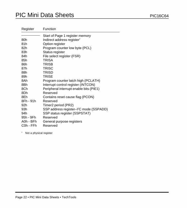
Register Function
Start of Page 1 register memory80h Indirect address register†
81h Option register82h Program counter low byte (PCL)83h Status register84h File select register (FSR)85h TRISA86h TRISB87h TRISC88h TRISD89h TRISE8Ah Program counter latch high (PCLATH)8Bh Interrupt control register (INTCON)8Ch Peripheral interrupt enable bits (PIE1)8Dh Reserved8Eh Contains reset cause flag (PCON)8Fh - 91h Reserved92h Timer2 period (PR2)93h SSP address register–I2C mode (SSPADD)94h SSP status register (SSPSTAT)95h - 9Fh ReservedA0h - BFh General purpose registersC0h - FFh Reserved
† Not a physical register
PIC16C64

TechTools • PIC Mini Data Sheets • Page 23
PIC Mini Data Sheets
DS
PIC16C64
PAGE 0
W register
Stack (8)
INDIRECT
TMR0
PCL
STATUS
FSR
PORTA
PORTB
PORTC
PORTD
PORTE
PCLATH
INTCON
PIR1
TMR1L
TMR1H
T1CON
TMR2
T2CON
SSPBUF
SSPCON
CCPR1L
CCPR1H
CCP1CON
GeneralPurposeRegisters
PAGE 1
W register
Stack (8)
INDIRECT
OPTION
PCL
STATUS
FSR
TRISA
TRISB
TRISC
TRISD
TRISE
PCLATH
INTCON
PIE1
PCON
PR2
SSPADD
SSPSTAT
GeneralPurpose
80h
81h
82h
83h
84h
85h
86h
87h
88h
89h
8Ah
8Bh
8Ch
8Dh
8Eh
8Fh
90h
91h
92h
93h
94h
95h
9Fh
A0h
BFh
C0h
FF
00h
01h
02h
03h
04h
05h
06h
07h
08h
09h
0Ah
0Bh
0Ch
0Dh
0Eh
0Fh
10h
11h
12h
13h
14h
15h
16h
17h
18h
1Fh
20h
7Fh

Page 24 • PIC Mini Data Sheets • TechTools
PIC Mini Data Sheets
PIC16C64 Register Description
• W (working register): The W register holds the second operandin two-operand instructions and is used for internal data transfer.The W register is similar to the accumulator in other processors.
• Stack. The stack is comprised of eight registers which are used forcalling and returning from subroutines. The program counter ispushed onto the stack when a CALL is executed or an interrupt isacknowledged. The stack is popped in the event of a RET, RETW,or RETI instruction.
• Indirect Addressing Registers (00h & 80h). These registers don'tactually exist. Naming register 00h or 80h in an instruction causesthe PIC to read the register pointed to by register 04h (file selectregister). Register 04h should contain the address of a register toread or write.
• Timer0 (01h: TMR0). TMR0 replaces RTCC, and is similar infunction. TMR0 is an 8-bit overflow counter. The clock is drivenexternally through the TMR0 pin, or internally by OSC/4. Whendriven externally, the TMR0 module can be selected to incrementon either low-to-high or high-to-low transitions. TMR0 has aprogrammable prescaler option, assigned through the OPTIONregister. The maximum external clock frequency is 50 MHz. Seethe Microchip PIC16C64 data sheet for details concerning externaltiming characteristics for TRM0.
• Program Counter Low Byte (02h: PCL). The program counterholds the address for the instruction currently being executed. Theprogram counter and its associated eight-level stack are 13 bitswide, with PCL holding the lower 8 bits and PCH holding the upper5 bits. PCH is automatically loaded when a JMP or CALL isperformed. Although PCH is not addressable, your program canload PCH through the PCLATH register (see register f0A, later inthis section).
• Status register (03h). This register contains the status of thearithmetic logic unit (ALU), the reset status, and the page selectbits for register memory (not program memory, as in PIC16C5xdevices).
PIC16C64

TechTools • PIC Mini Data Sheets • Page 25
PIC Mini Data Sheets
DS
The function of each bit in the STATUS register is shown below:
Bit Label Name and Function
0 Carry bit (C). Set if an addition or subtraction causesan overflow from the most significant bit of the resultant(bit 7). Subtraction is included because it is executedby adding the two’s complement.
Also used by rotate instructions, which rotate thecontents of a register and copy the low or high orderbit of the register into the carry bit.
1 Digit carry bit (DC). Set if an addition or subtractioncauses an overflow from the 4th low order bit (bit 3).Digit carry indicates that more than one hex digit (4bits) was necessary to accommodate the result.
2 Zero bit (Z). Set if the result of an arithmetic or logicoperation is zero.
3 Power-down bit (PD). Set during power-up or by aCLRWDT (clear watchdog) instruction. Cleared by aSLEEP instruction.
4 Time-out bit (TO). Set during power-up, by CLRWDT,or by SLEEP. Cleared by a watchdog timer time-out.
The following table shows how various events affectthe STATUS register power-down(PD) and time-out(TO) bits:
Event PD TO
Power-up 1 1Watchdog time-out x 0SLEEP instruction 0 1CLRWDT instruction 1 1
The following table shows the status of the power-down and time-out bits after a reset:
PIC16C64

Page 26 • PIC Mini Data Sheets • TechTools
PIC Mini Data Sheets
Cause of Reset PD TO
Watchdog time-out (not during sleep) 1 0Watchdog time-out (during sleep) 0 0External reset (not during sleep) x xExternal reset (during sleep) 0 1Normal power-up 1 1
5-6 Register page select bits (RP0, RP1). These bitsdetermine which register page is selected for directaddressing operations. Each page is 128 bytes long,so only RP0 is valid in the PIC16C64. Future PICsmay require RP1, so using this bit for general storagemay prevent upward compatibility.
7 Page select bit for indirect addressing (IRP). The IRPbit is not used. Future PICs may require IRP, so usingthis bit for general storage may prevent upwardcompatibility.
• File Select Register (04h: FSR). This register selects the registerfor indirect addressing. Bits 0-7 select 1 of 256 registers in thecurrent bank. As described in the PIC16C5x register descriptions,a read or write to register 00h will access the register pointed to bythe FSR.
• I/O Port A (05h: RA or Port A). 6-bit I/O port. This register is forreading and writing I/O Port A. It can be read and written just as anyother register. Read instructions always read the I/O pins, however,regardless of whether the pins are programmed as inputs oroutputs.
Bit 4 is a Schmitt trigger input and an open-collector output andshares its pin with the TMR0 clock input.
• I/O Port B (06h: RB or Port B). 8-bit I/O port. Each of the Port B pinshas a weak internal pull-up resistor (~100 µA). A pin’s pull-up isturned off if the pin is configured as an output, and a single bit inthe OPTION register can turn off all the pull-ups. The pull-upresistors are disabled on power-on reset.
PIC16C64
TechTools • PIC Mini Data Sheets • Page 27
PIC Mini Data Sheets
DS
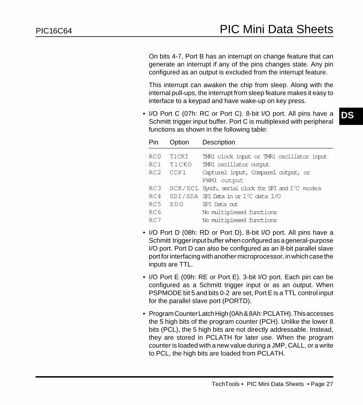
On bits 4-7, Port B has an interrupt on change feature that cangenerate an interrupt if any of the pins changes state. Any pinconfigured as an output is excluded from the interrupt feature.
This interrupt can awaken the chip from sleep. Along with theinternal pull-ups, the interrupt from sleep feature makes it easy tointerface to a keypad and have wake-up on key press.
• I/O Port C (07h: RC or Port C). 8-bit I/O port. All pins have aSchmitt trigger input buffer. Port C is multiplexed with peripheralfunctions as shown in the following table:
Pin Option Description
RC0 T1CKI TMR1 clock input or TMR1 oscillator inputRC1 T1CKO TMR1 oscillator outputRC2 CCP1 Capture1 input, Compare1 output, or
PWM1 outputRC3 SCK/SCL Synch. serial clock for SPI and I 2C modesRC4 SDI/SDA SPI Data in or I 2C data I/ORC5 SDO SPI Data outRC6 No multiplexed functionsRC7 No multiplexed functions
• I/O Port D (08h: RD or Port D). 8-bit I/O port. All pins have aSchmitt trigger input buffer when configured as a general-purposeI/O port. Port D can also be configured as an 8-bit parallel slaveport for interfacing with another microprocessor, in which case theinputs are TTL.
• I/O Port E (09h: RE or Port E). 3-bit I/O port. Each pin can beconfigured as a Schmitt trigger input or as an output. WhenPSPMODE bit 5 and bits 0-2 are set, Port E is a TTL control inputfor the parallel slave port (PORTD).
• Program Counter Latch High (0Ah & 8Ah: PCLATH). This accessesthe 5 high bits of the program counter (PCH). Unlike the lower 8bits (PCL), the 5 high bits are not directly addressable. Instead,they are stored in PCLATH for later use. When the programcounter is loaded with a new value during a JMP, CALL, or a writeto PCL, the high bits are loaded from PCLATH.
PIC16C64
Page 28 • PIC Mini Data Sheets • TechTools
PIC Mini Data Sheets
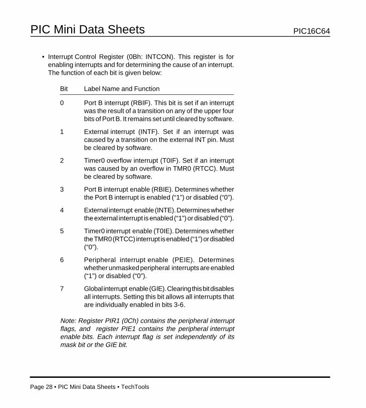
• Interrupt Control Register (0Bh: INTCON). This register is forenabling interrupts and for determining the cause of an interrupt.The function of each bit is given below:
Bit Label Name and Function
0 Port B interrupt (RBIF). This bit is set if an interruptwas the result of a transition on any of the upper fourbits of Port B. It remains set until cleared by software.
1 External interrupt (INTF). Set if an interrupt wascaused by a transition on the external INT pin. Mustbe cleared by software.
2 Timer0 overflow interrupt (T0IF). Set if an interruptwas caused by an overflow in TMR0 (RTCC). Mustbe cleared by software.
3 Port B interrupt enable (RBIE). Determines whetherthe Port B interrupt is enabled (“1”) or disabled (“0”).
4 External interrupt enable (INTE). Determines whetherthe external interrupt is enabled (“1”) or disabled (“0”).
5 Timer0 interrupt enable (T0IE). Determines whetherthe TMR0 (RTCC) interrupt is enabled (“1”) or disabled(“0”).
6 Peripheral interrupt enable (PEIE). Determineswhether unmasked peripheral interrupts are enabled(“1”) or disabled (“0”).
7 Global interrupt enable (GIE). Clearing this bit disablesall interrupts. Setting this bit allows all interrupts thatare individually enabled in bits 3-6.
Note: Register PIR1 (0Ch) contains the peripheral interruptflags, and register PIE1 contains the peripheral interruptenable bits. Each interrupt flag is set independently of itsmask bit or the GIE bit.
PIC16C64

TechTools • PIC Mini Data Sheets • Page 29
PIC Mini Data Sheets
DS
• Peripheral Interrupt Register (0Ch: PIR1). This register containsinterrupt flag bits. Interrupt flags are set by interrupt events,regardless of whether or not some or all interrupts are disabled.Before enabling interrupts, clear the interrupt flag to prevent ajump to the interrupt service routine.
Bit Label Name and Function
0 Timer1 interrupt flag (TMR1IF). When set, TMR1 hasoverflowed, and TMR1IF must be cleared in software.When clear, TMR1 has not overflowed.
1 Timer2 interrupt flag (TMR2IF). When set, TMR2 hasoverflowed, and TMR2IF must be cleared in software.When clear, TMR2 has not overflowed.
2 Capture1/Compare1/PWM1 interrupt flag(CCP1IF).
In Capture mode, if CCP1IF is set, a TMR1 capturehas occurred. In Compare mode, if CCP1IF is set, aTMR1 compare match has occurred.
Both set conditions must be cleared in software. Aclear setting in either mode means that thecorresponding condition did not occur.
The PWM Mode for CCP1IF is not used.
3 Synchronous serial port interrupt flag (SSPIF). If set,a transmit or receive has been completed. If clear, theport is waiting to transmit or receive.
4-6 Unimplemented and read as “0”.
7 Parallel slave port read/write interrupt flag (PSPIF).If set, a read or a write operation has taken place. Thiscondition must be cleared in software. If clear, noread or write has occurred.
PIC16C64

Page 30 • PIC Mini Data Sheets • TechTools
PIC Mini Data Sheets
• Timer1 (OEh, OFh: TMR1L, TMR1H). These are the low and highbytes that comprise the 16-bit Timer1. The clock source can beeither internal (OSC/4) or external. When the clock source isexternal, TMR1 can run either synchronously or asynchronously.In asynchronous mode, TMR1 can run during sleep. When usedwith CCP1, TMR1 functions synchronously as a time base for 16-bit compare or capture.
• Timer1 Control Register (10h: T1CON).
Bit Label Name and Function
0 Timer1 run bit (TMR1ON). Set enables TMR1. Clearstops TMR1.
1 Timer1 clock select (TMR1CS). If set, use externalclock, low-to-high transition, through TCKI pin. Ifclear, use internal clock (OSC/4).
2 Timer1 external clock input synchronization control(T1INSYNC). If TMR1CS is set, then if T1INSYNC isset , do not synchronize external clock input, otherwiseif clear, synchronize external clock input. If TMR1CSis clear, then T1INSYNC is ignored.
3 Timer1 oscillator enable/disable (T1OSCEN). If set,then the oscillator is enabled. If clear, the oscillator isshut off, reducing power use.
4-5 Timer1 input clock prescale select register (T1CKPS0,T1CKPS1).
Bits 5-4 Prescale Value
11 810 401 200 1
6-7 Unimplemented and read as “0”.
PIC16C64
TechTools • PIC Mini Data Sheets • Page 31
PIC Mini Data Sheets
DS
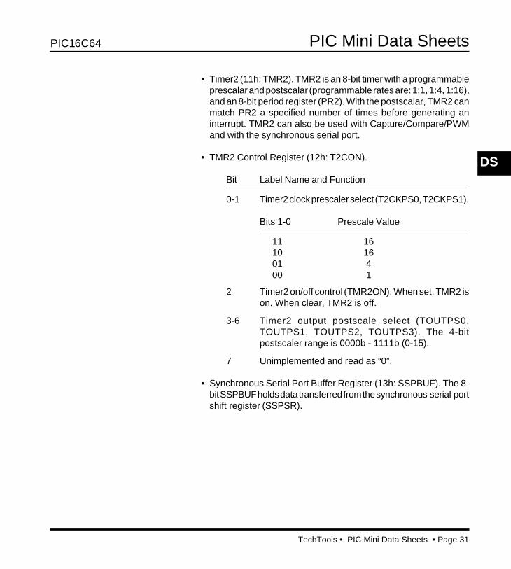
• Timer2 (11h: TMR2). TMR2 is an 8-bit timer with a programmableprescalar and postscalar (programmable rates are: 1:1, 1:4, 1:16),and an 8-bit period register (PR2). With the postscalar, TMR2 canmatch PR2 a specified number of times before generating aninterrupt. TMR2 can also be used with Capture/Compare/PWMand with the synchronous serial port.
• TMR2 Control Register (12h: T2CON).
Bit Label Name and Function
0-1 Timer2 clock prescaler select (T2CKPS0, T2CKPS1).
Bits 1-0 Prescale Value
11 1610 1601 400 1
2 Timer2 on/off control (TMR2ON). When set, TMR2 ison. When clear, TMR2 is off.
3-6 Timer2 output postscale select (TOUTPS0,TOUTPS1, TOUTPS2, TOUTPS3). The 4-bitpostscaler range is 0000b - 1111b (0-15).
7 Unimplemented and read as “0”.
• Synchronous Serial Port Buffer Register (13h: SSPBUF). The 8-bit SSPBUF holds data transferred from the synchronous serial portshift register (SSPSR).
PIC16C64

Page 32 • PIC Mini Data Sheets • TechTools
PIC Mini Data Sheets
• Synchronous Serial Port Control Register (14h: SSPCON).
Bit Label Name and Function
0-3 Synchronous serial port mode select (SSPM0,SSPM1, SSPM2, SSPM3):
Bits 3-0 Mode
0000 SPI master mode, clock=OSC/40001 SPI master mode, clock=OSC/160010 SPI master mode, clock=OSC/640011 SPI master mode, clock=TMR2 output/20100 SPI slave mode, clock=SCK pin.
SS pin control enabled.0101 SPI slave mode, clock=SCK pin.
SS pin control disabled.SS is available for I/O.
0110 I2C slave mode, 7-bit address.0111 I2C slave mode, 10-bit address.1011 I2C master mode support enabled
(slave idle).1110 I2C slave mode, 7-bit address with
master mode support enabled.1111 I2C slave mode, 10-bit address with
master mode support enabled.
4 Clock polarity select (CKP).
In SPI mode: If this bit is set, the transmit occurs onhigh-to-low transitions, and the clock's idle state ishigh. If clear, the transmit occurs on low-to-hightransitions, and the clock's idle state is low.
In I2C mode: This bit is for SCK release control. If set,the clock is enabled. If clear, the clock is stretched byholding it low. (This ensures enough time to set updata.)
PIC16C64
TechTools • PIC Mini Data Sheets • Page 33
PIC Mini Data Sheets
DS
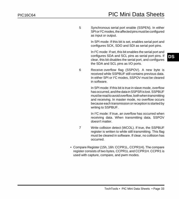
5 Synchronous serial port enable (SSPEN). In eitherSPI or I2C modes, the affected pins must be configuredas input or output.
In SPI mode: If this bit is set, enables serial port andconfigures SCK, SDO and SDI as serial port pins.
In I2C mode: If set, this bit enables the serial port andconfigures SDA and SCL pins as serial port pins. Ifclear, this bit disables the serial port, and configuresthe SDA and SCL pins as I/O ports.
6 Receive overflow flag (SSPOV). A new byte isreceived while SSPBUF still contains previous data.In either SPI or I2C modes, SSPOV must be clearedin software.
In SPI mode: If this bit is true in slave mode, overflowhas occurred, and the data in SSPSR is lost. SSPBUFmust be read to avoid overflow, both when transmittingand receiving. In master mode, no overflow occursbecause each transmission or reception is started bywriting to SSPBUF.
In I2C mode: If true, an overflow has occurred whenreceiving data. When transmitting data, SSPOVdoesn't matter.
7 Write collision detect (WCOL). If true, the SSPBUFregister is written to while still transmitting. This flagmust be cleared in software. If clear, no collision hasoccurred.
• Compare Register (15h, 16h: CCPR1L, CCPR1H). The compareregister consists of two bytes, CCPR1L and CCPR1H. CCPR1 isused with capture, compare, and pwm modes.
PIC16C64
Page 34 • PIC Mini Data Sheets • TechTools
PIC Mini Data Sheets
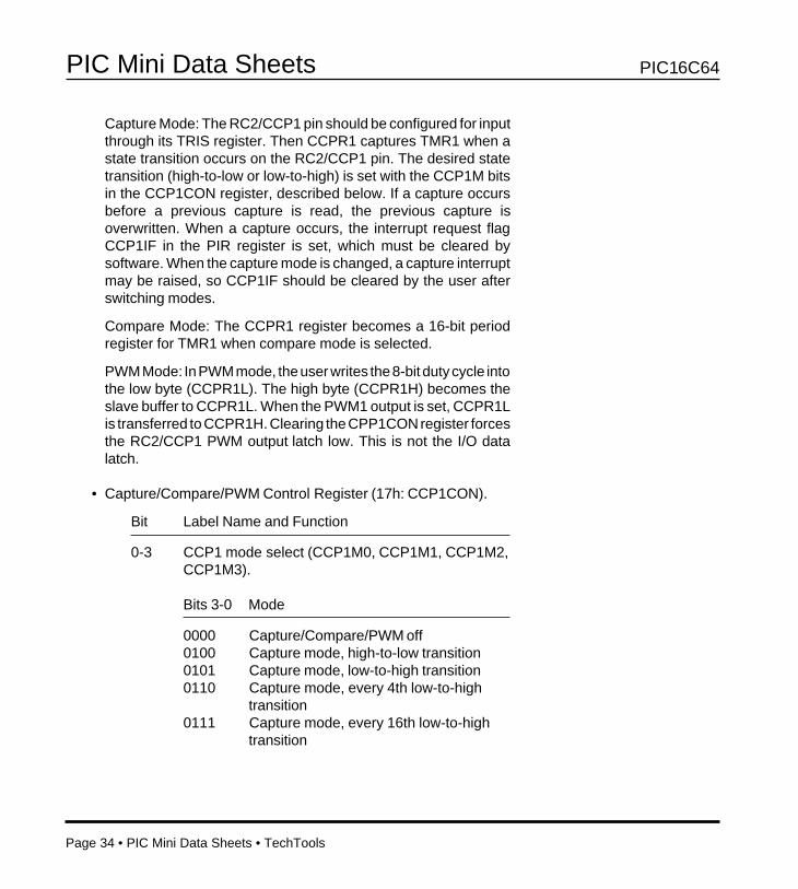
Capture Mode: The RC2/CCP1 pin should be configured for inputthrough its TRIS register. Then CCPR1 captures TMR1 when astate transition occurs on the RC2/CCP1 pin. The desired statetransition (high-to-low or low-to-high) is set with the CCP1M bitsin the CCP1CON register, described below. If a capture occursbefore a previous capture is read, the previous capture isoverwritten. When a capture occurs, the interrupt request flagCCP1IF in the PIR register is set, which must be cleared bysoftware. When the capture mode is changed, a capture interruptmay be raised, so CCP1IF should be cleared by the user afterswitching modes.
Compare Mode: The CCPR1 register becomes a 16-bit periodregister for TMR1 when compare mode is selected.
PWM Mode: In PWM mode, the user writes the 8-bit duty cycle intothe low byte (CCPR1L). The high byte (CCPR1H) becomes theslave buffer to CCPR1L. When the PWM1 output is set, CCPR1Lis transferred to CCPR1H. Clearing the CPP1CON register forcesthe RC2/CCP1 PWM output latch low. This is not the I/O datalatch.
• Capture/Compare/PWM Control Register (17h: CCP1CON).
Bit Label Name and Function
0-3 CCP1 mode select (CCP1M0, CCP1M1, CCP1M2,CCP1M3).
Bits 3-0 Mode
0000 Capture/Compare/PWM off0100 Capture mode, high-to-low transition0101 Capture mode, low-to-high transition0110 Capture mode, every 4th low-to-high
transition0111 Capture mode, every 16th low-to-high
transition
PIC16C64

TechTools • PIC Mini Data Sheets • Page 35
PIC Mini Data Sheets
DS
Bits 3-0 Mode
1000 Compare mode, set output on match1001 Compare mode, clear output on match1010 Compare mode, raise software interrupt,
setting CCP1IF bit.1011 Compare mode, trigger special event11?? PWM mode
4-5 Two low-order bits (CCP1X, CCP1Y). Used only forPWM. Write these two bits in high resolution (10-bit)mode, or keep them constant at “0” when only 8-bitresolution is desired.
6-7 Unimplemented, read as “0”.
• General Purpose Registers (20h - 7Fh). These registers are foruse by your program.
• Option Register (81h): This register sets prescaler options, TMR0settings, external interrupt trigger edge, and PORTB pull-upstatus. The function of each bit is shown below:
Bit Label Name and Function
0-2 Prescaler ratio (PS0, PS1, PS2). These 3 bitsdetermine the prescaler input-to-output ratio. Whenusing the prescaler with TMR0, the seven possibleratios are 1:2, 1:4, 1:8, 1:16, 1:32, 1:64, 1:128, 1:256.When using the prescaler with the watchdog timer,the ratios are 1:1, 1:2, 1:4, 1:8, 1:16, 1:32, 1:64,1:128.
For example, assign the prescaler to the watchdogtimer. To increase the watchdog time-out period to 64times its normal length, set the prescaler ratio to110b; this yields a watchdog period of approximately1 second (64 x 18 ms).
PIC16C64

Page 36 • PIC Mini Data Sheets • TechTools
PIC Mini Data Sheets
Bit Label Name and Function
3 Prescaler assignment (PSA). This bit determineswhether the prescaler is assigned to TMR0 (“0”) or tothe watchdog timer (“1”).
4 Timer0 trigger edge (RTE). This bit determineswhether TMR0 increments on a low-to-high (“0”) orhigh-to-low (“1”) transition on the T0CKI pin.
5 Timer0 signal source (RTS). This bit determineswhether TMR0 is driven by the PIC's internalinstruction clock (“0”) or by the T0CKI pin (“1”).
6 External interrupt trigger edge (INTEDG). Determineswhether an interrupt will be caused by a high-to-low(“0”) or low-to-high (“1”) transition on the external INTpin.
7 PORTB pull-up status (RBPU). If this bit is clear,PORTB pull-up resistors are enabled on pins that areinputs. If this bit is set, all Port B pull-ups are disabled.
• Program Counter Low Byte (82h: PCL). Same as register 02h.
• Status Register (83h). Same as register 03h.
• File Select Register (84h: FSR). Same as register 04h.
• Data Direction Register for Port A (85h: TRISA). This is the datadirection register for Port A. In the Microchip data book, thisregister is referred to as “Tri-State A”, hence “TRISA” as anabbreviation. Data direction registers in the PIC16C64 areaddressable, unlike their counterparts in PIC16C5x devices.
Bits in this register which are set to “1” cause the correspondingbits in Port A to become inputs (the pins go into high impedancemode, allowing them to be driven by an external source). Bitswhich are cleared to “0” cause the corresponding bits in Port A tobecome outputs.
PIC16C64

TechTools • PIC Mini Data Sheets • Page 37
PIC Mini Data Sheets
DS
• Data Direction Register for Port B (86h: TRISB). This is the datadirection register for Port B. The bits are set similarly to TRISA.
• Data Direction Register for Port C (87h: TRISC). This is the datadirection register for Port C. The bits are set similarly to TRISA.
• Data Direction Register for Port D (88h: TRISD). This is the datadirection register for Port D. The bits are set similarly to TRISA.
• Data Direction Register or Parallel Slave Port Mode Register forPort E (89h: TRISE). The following table describes the TRISEregister:
Bit Label Name and Function
0 Data Direction Bit (TRISE0). This bit is set similarlyto TRISA when Port E is used for general-purpose I/O. When Port E is used for parallel slave port control(PSPMODE), This bit must be set.
1 Data Direction Bit (TRISE1). This bit is set similarlyto TRISA when Port E is used for general-purpose I/O. When Port E is used for parallel slave port control(PSPMODE), this bit must be set.
2 Data Direction Bit (TRISE2). This bit is set similarlyto TRISA when Port E is used for general-purpose I/O. When Port E is used for parallel slave port control(PSPMODE), this bit must be set.
3 Not used. Read as “0”.
4 Parallel Slave Port Mode (PSPMODE). This bit selectsthe parallel slave port mode for ports A and E whenset, and bits 0 - 2 (above) must be set. When clear,Port E is a general-purpose I/O port.
PIC16C64

Page 38 • PIC Mini Data Sheets • TechTools
PIC Mini Data Sheets
Bit Label Name and Function
5 Input Buffer Overflow (IBOV). This bit indicateswhether or not an input buffer overflow has occurred.If set, a write occurred before previous input wasread. This bit must be cleared in software. If clear,overflow has not occurred.
6 Output Buffer Full (OBF). This bit indicates whetheror not the output buffer is full. If set, the output bufferholds a previously written word. If clear, the outputbuffer has been read.
7 Input Buffer Full (IBF). This bit indicates whether ornot the input buffer is full. If set, a word has beenreceived and is waiting to be read by the CPU. If clear,no word has been received.
• Program Counter Latch High (8Ah: PCLATH). Same as register0Ah.
• Interrupt Control Register (8Bh: INTCON). Same as register 0Bh.
• Enable Bits for Peripheral Interrupts (8Ch: PIE1):
Bit Label Name and Function
0 Timer1 interrupt enable bit (TMR1IE). If set, enablesTMR1IF interrupt. If clear, disables TMR1IF interrupt.
1 Timer2 interrupt enable bit (TMR2IE). If set, enablesTMR2IF interrupt. If clear, disables TMR2IF interrupt.
2 CCP1 interrupt enable bit (CCP1IE). If set, enablesCCP1IF interrupt. If clear, disables CCP1IF interrupt.
3 Synchronous serial port interrupt enable bit (SSPIE).If set, enables SSPIF interrupt. If clear, disablesSSPIF interrupt.
PIC16C64

TechTools • PIC Mini Data Sheets • Page 39
PIC Mini Data Sheets
DS
Bit Label Name and Function
4-6 Unimplemented and read as “0”.
7 Parallel slave port interrupt enable (PSPIE). If set,enables PSPIF interrupt. If clear, disables interrupt.
• PCON Register (8Eh): Flags for differentiating between a power-on reset, an external MCLR reset, and a WDT reset:
Bit Label Name and Function
0 Reserved. Should be programmed as “1”.
1 Power-on-reset flag (POR). If set, no power-on-reset.If clear, a power-on-reset has occurred. Must be setby software after a power-on-reset.
2-7 Unimplemented. Read as “0”.
• Timer2 Period Register (92h: PR2). Read/write register for settingperiod of TMR2.
• SSP (I2C) Slave Address Register (93h: SSPADD). In 10-bit mode,write the high byte of the address (1111 0 A9 A8 0). After the highbyte address match, load the low byte address (A7 - A0).
• Synchronous Serial Port Status Register (94h: SSPSTAT):
Bit Label Name and Function
0 Buffer full (BF).
Receive Mode: If set, reception is complete andSSPBUF is full. If clear, reception is not complete,and SSPBUF is empty.
Transmit Mode: If set, transmission is occurring, andSSPBUF is full. If clear, transmission is complete andSSPBUF is empty.
PIC16C64

Page 40 • PIC Mini Data Sheets • TechTools
PIC Mini Data Sheets
Bit Label Name and Function
1 Update address (UA). 10-bit I2C slave mode only. Ifset, the user needs to update the address in theSSPADD register. If clear, the address is current.
2 Read/Write bit information (R_W). I2C mode only.This bit holds the R/W bit information received followingthe last address match. This bit is only valid during thetransmission, and can be used to determine whethertransmission or reception is in progress. If set, a readis in progress. If clear, a write is in progress.
3 Start bit (S). I2C mode only. Cleared when the SSPmodule is disabled (SSPEN cleared). If set, indicatesthat a start bit has been detected last. This bit is clearon reset. If clear, the start bit was not detected last.
4 Stop bit (P). I2C mode only. Cleared when the SSPmodule is disabled (SSPEN is cleared). If set, indicatesthat a stop bit was detected last. If clear, a stop bit wasnot detected last.
5 Data/Address bit (D_A). I2C mode only. If set, indicatesthat the last byte received was data. If clear, indicatesthat the last byte received was an address.
6-7 Unimplemented and read as “0”.
• General Purpose Registers (A0h - BFh). These registers are foruse by your program.
PIC16C64

TechTools • PIC Mini Data Sheets • Page 41
PIC Mini Data Sheets
DS
PIC16C71 Pin-OutThe following diagram shows the PIC16C71 pin-out:
Pin Function
RA0 - RA4 I/O Port ARB0 - RB7 I/O Port BAIN0 - AIN3 Analog inputsVREF External reference for A/DINT External interrupt inputRTCC Real-time clock/counter inputMCLR Master clear (reset)OSC1 Oscillator inputOSC2/CLKOUT Oscillator output (OSC/4)Vdd Power supplyVss GroundVpp Programming voltage input
RA2/AIN2
RA3/AIN3/VREF
RA4/RTCC
MCLR/Vpp
Vss
RB0/INT
RB1
RB2
RB3
RA1/AIN1
RA0/AIN0
OSC1
OSC2/CLKOUT
Vdd
RB7
RB6
RB5
RB4
1
2
3
4
5
6
7
8
9
18
17
16
15
14
13
12
11
10
PIC16C71
PDIPCERDIP
SOIC
PIC16C71

Page 42 • PIC Mini Data Sheets • TechTools
PIC Mini Data Sheets
PIC16C71 MicrocontrollersThe table below shows the various PIC16C71’s available:
PART # ERASE (E)PROM RAM I/O SUPPLY OSC. FREQ.
PIC16C71-04 No 1K x 14 36 x 8 13 4.0 - 6.0 V RC,XTAL DC - 4 MHzPIC16C71-16 No 1K x 14 36 x 8 13 4.0 - 6.0 V RC,XTAL DC - 16 MHzPIC16C71/JW Yes 1K x 14 36 x 8 13 4.0 - 6.0 V RC,XTAL DC - 16 MHz
PIC16LC71-04 No 1K x 14 36 x 8 13 3.0 - 6.0 V RC,XTAL DC - 4 MHz
New and Modified FeaturesAlthough the PIC16C71 is much like devices in the PIC16C5x family, ithas a number of important differences:
• Interrupts possible from four sources: external pin, RTCC timer, A/D conversion, and change on four Port B pins.
• Port B modifications. Software controlled pull-up’s have beenadded, along with the ability to generate an interrupt when any offour pins changes state.
• 8-bit analog-to-digital convertor. Four channel multiplexed A/D convertor has 20 mS conversion time, ±1 LSB accuracy, andbuilt-in sample and hold.
• 8-level hardware stack. Allows deeper nesting of subroutines.
• 14-bit instruction word. Provides larger page sizes for programmemory (2K) and RAM (128 bytes).
• New timers. Two new timers have been added to avoid unneces-sary delays on power-up and wake-up. These timers are theoscillator start-up timer (OST) and power-up timer (PWRT).
• New I/O pin. An additional I/O pin has been added as bit 4 of PortA. This is physically implemented on pin 3 (RTCC/RA4).
• Status register changes. Program page select bits (bit 5-6) havebeen replaced by register page select bits.
PIC16C71

TechTools • PIC Mini Data Sheets • Page 43
PIC Mini Data Sheets
DS
• File select register changes. The FSR has been increased to 8bits, and bits 5-6 no longer function as register page select(register page selection is now done in the Status register).
• High byte added to PC. A high byte has been added to the programcounter to handle program memory paging.
• Page select bits removed. Program memory page select bits in theStatus register (PA0 - PA2) have been removed.
The part’s 1K of program space can be utilized without worryingabout page boundaries.
• Register 07h is unimplemented. This register cannot be used forstorage, as it can in 18-pin PIC16C5x devices.
• Reset vector changed to 0000h.
• Interrupt vector added at 0004h.
PIC16C71

Page 44 • PIC Mini Data Sheets • TechTools
PIC Mini Data Sheets
PIC16C71 RegistersThe following table shows the various registers in the PIC16C71; thefunction of each register is described in the following pages.
Register Function
- W register00h Indirect addressing register01h Real-time clock/counter (RTCC)02h Program counter low byte (PCL)- Stack registers (8)03h Status register04h File select register (FSR)05h I/O Port A06h I/O Port B07h Not implemented08h A/D control & status register (ADCON0)09h A/D result (ADRES)0Ah Program counter latch high (PCLATH)0Bh Interrupt control register (INTCON)0Ch - 2Fh General purpose registers30h - 7Fh Not implemented
End of page 0 register memory
80h Indirect addressing register81h Option register82h Program counter low byte (PCL)83h Status register84h File select register (FSR)85h TRISA86h TRISB87h Not implemented88h A/D control register (ADCON1)89h A/D result (ADRES)8Ah Program counter latch high (PCLATH)8Bh Interrupt control register (INTCON)8Ch - AFh Reads/writes registers 0Ch - 2FhB0h - FFh Not implemented
PIC16C71

TechTools • PIC Mini Data Sheets • Page 45
PIC Mini Data Sheets
DS
PIC16C71
PAGE 0
W register
Stack (8)
Indirect addr.
RTCC
PCL
STATUS
FSR
PORT A
PORT B
ADCON0
ADRES
PCLATH
INTCON
36
general
purpose
registers
(RAM)
PAGE 1
W register
Stack (8)
Indirect addr.
OPTION
PCL
STATUS
FSR
TRISA
TRISB
ADCON1
ADRES
PCLATH
INTCON
reads/writes
registers
0Ch - 2Fh
00h
01h
02h
03h
04h
05h
06h
07h
08h
09h
0Ah
0Bh
0Ch
2Fh
30h
7Fh
80h
81h
82h
83h
84h
85h
86h
87h
88h
89h
8Ah
8Bh
8Ch
AFh
B0h
FFh

Page 46 • PIC Mini Data Sheets • TechTools
PIC Mini Data Sheets
The following text describes the function of each new or modifiedregister. Refer to the PIC16C5x section for registers not shown here.
For some of the registers, you’ll notice the designation “xxh” following theregister name. This indicates the address of the register. Registers withno address cannot be addressed directly.
• Program Counter Low Byte (02h: PCL). The program counterholds the address for the instruction currently being executed. Theprogram counter and its associated eight-level stack are 13 bitswide, with PCL holding the lower 8 bits and PCH holding the upper5 bits. PCH is automatically loaded when a JMP or CALL isperformed. Although PCH is not addressable, your program canload PCH through the PCLATH register (see register f0A, later inthis section).
• Stack. The stack is comprised of eight registers which are used forcalling and returning from subroutines. The program counter ispushed onto the stack when a CALL is executed or an interrupt isacknowledged. The stack is popped in the event of a RET, RETW,or RETI instruction.
• Status Register (03h). This register contains the status of thePIC’s arithmetic logic unit (ALU), the reset status, and the pageselect bits for register memory (not program memory, as inPIC16C5x devices).
The function of each bit in the status register is shown below:
Bit Function
0 Carry bit (C). Set if an addition or subtraction causesan overflow from the most significant bit of the result-ant (bit 7). Subtraction is included because it’s ex-ecuted by adding the two’s complement.
Also used by rotate instructions, which rotate thecontents of a register and copy the low or high orderbit of the register into the carry bit.
PIC16C71

TechTools • PIC Mini Data Sheets • Page 47
PIC Mini Data Sheets
DS
Bit Function
1 Digit carry bit (DC). Set if an addition or subtractioncauses an overflow from the 4th low order bit (bit 3).Digit carry indicates that more than one hex digit (4bits) was necessary to accommodate the result.
2 Zero bit (Z). Set if the result of an arithmetic or logicoperation is zero.
3 Power-down bit (PD). Set during power-up or by aCLR WDT (clear watchdog) instruction. Cleared by aSLEEP instruction.
4 Time-out bit (TO). Set during power-up, by CLRWDT, or by SLEEP. Cleared by a watchdog timertime-out.
5-6 Register page select bits for direct addressing (RP0,RP1). These bits determine which register page isselected for direct addressing operations. Each pageis 128 bytes long, so only RP0 is valid in a PIC16C71.RP1 can be used for storage, but may have an actualuse in future PIC’s.
7 Register page select bit for indirect addressing (IRP).This bit determines which register page is selectedfor indirect addressing operations. Since each “indi-rect” page is 256 bytes long, however, it is not valid inthe PIC16C71. IRP can be used for storage, but mayhave an actual use in future PIC’s.
PIC16C71
Page 48 • PIC Mini Data Sheets • TechTools
PIC Mini Data Sheets
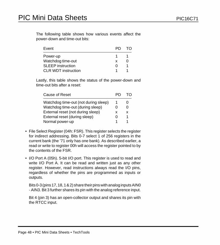
The following table shows how various events affect thepower-down and time-out bits:
Event PD TO
Power-up 1 1Watchdog time-out x 0SLEEP instruction 0 1CLR WDT instruction 1 1
Lastly, this table shows the status of the power-down andtime-out bits after a reset:
Cause of Reset PD TO
Watchdog time-out (not during sleep) 1 0Watchdog time-out (during sleep) 0 0External reset (not during sleep) x xExternal reset (during sleep) 0 1Normal power-up 1 1
• File Select Register (04h: FSR). This register selects the registerfor indirect addressing. Bits 0-7 select 1 of 256 registers in thecurrent bank (the ’71 only has one bank). As described earlier, aread or write to register 00h will access the register pointed to bythe contents of the FSR.
• I/O Port A (05h). 5-bit I/O port. This register is used to read andwrite I/O Port A. It can be read and written just as any otherregister. However, read instructions always read the I/O pins,regardless of whether the pins are programmed as inputs oroutputs.
Bits 0-3 (pins 17, 18, 1 & 2) share their pins with analog inputs AIN0- AIN3. Bit 3 further shares its pin with the analog reference input.
Bit 4 (pin 3) has an open-collector output and shares its pin withthe RTCC input.
PIC16C71

TechTools • PIC Mini Data Sheets • Page 49
PIC Mini Data Sheets
DS
Two bits in ADCON1 (f88) determine whether bits 0-3 are digitalor analog pins. Upon power-on reset, bits 0-3 are configured asanalog inputs.
• I/O Port B (06h). 8-bit I/O port. Each of the Port B pins has a weakinternal pull-up resistor (~250 µA). A pin’s pull-up is turned off if thepin is configured as an output, and a single bit in the Option registercan turn off all the pull-ups. The pull-up resistors are disabled onpower-on reset.
On bits 4-7 (pins 10-13), Port B has an interrupt on change featurethat can generate an interrupt if any of the pins changes state. Anypin configured as an output is excluded.
This interrupt can wake up the chip from sleep. Along with theinternal pull-ups, the interrupt from sleep feature makes it easy tointerface to a keypad and have wake-up on key press.
• A/D Control and Status Register (08h: ADCON0). This registercontrols the PIC16C71’s analog-to-digital convertor; it also re-ports the status of the A/D. The functions of the various bits areshown below:
Bit Function
0 A/D enable. This bit determines whether or not the A/D convertor is on or off. When turned off, the A/Dconvertor consumes no current.
1 A/D interrupt. Set if an interrupt was the result of anA/D conversion. Must be cleared by software.
2 Go/done bit. Must be set to “1” to start a conversion.Cleared by hardware when conversion is complete.
3-4 Analog channel select. These bits determine whichinput pin will be used for the A/D convertor. “00”selects AIN0, “01” selects AIN1, “10” selects AIN2,and “11” selects AIN3.
5 General purpose bit. Can be used for storage.
PIC16C71

Page 50 • PIC Mini Data Sheets • TechTools
PIC Mini Data Sheets
Bit Function
6-7 A/D conversion clock source. These bits determinethe clock source for the A/D convertor. The clock canbe derived from either the OSC1 input or from the A/D’s on-chip RC oscillator, as follows:
Bits Clock Source
00 2 x Tosc
01 8 x Tosc
10 32 x Tosc
11 RC oscillator (2-6 µs, 4 µs typical)
Whatever source you choose, each clock periodmust be at least 2 µs. Thus, if you’re using a fastcrystal for OSC1, you will need to set the A/D clocksource bits to “01” or “10”. And if the OSC1 clock is 20MHz, then you would only have the option of using theA/D’s RC oscillator, since 20 MHz cannot be divideddown far enough to give the minimum 2 µs neces-sary.
The A/D’s RC oscillator can vary considerably withvoltage and temperature (2-6 µs).
Total conversion time for a single sample is ten clockperiods (20 µs minimum).
• A/D Conversion Result (09h: ADRES). This register holds theresult of the most recent conversion.
• Program Counter Latch High (0Ah: PCLATH). This register isused to access the 5 high bits of the program counter (PCH).Unlike the lower 8 bits (PCL), the 5 high bits are not directlyaddresable. Instead, they are stored in PCLATH for later use.When the program counter is loaded with a new value during aJMP, CALL, or a write to PCL, the high bits are loaded fromPCLATH.
PIC16C71

TechTools • PIC Mini Data Sheets • Page 51
PIC Mini Data Sheets
DS
• Interrupt Control Register (0Bh: INTCON). This register is used toenable interrupts and to determine what caused an interrupt. Thefunction of each bit is given below:
Bit Function
0 Port B interrupt. This bit is set if an interrupt was theresult of a transition on any of the upper four bits ofPort B. It will remain set until cleared by software.
1 External interrupt. Set if an interrupt was caused by atransition on the external INT pin. Must be cleared bysoftware.
2 RTCC overflow interrupt. Set if an interrupt wascaused by an overflow in the real-time clock/counter.Must be cleared by software.
3 Port B interrupt enable. Determines whether the PortB interrupt is enabled (“1”) or disabled (“0”).
4 External interrupt enable. Determines whether theexternal interrupt is enabled (“1”) or disabled (“0”).
5 RTCC interrupt enable. Determines whether theRTCC interrupt is enabled (“1”) or disabled (“0”).
6 A/D interrupt enable. Determines whether the A/Dconversion complete interrupt is enabled (“1”) ordisabled (“0”).
7 Global interrupt enable. Clearing this bit disables allinterrupts. Setting this bit allows all interrupts that areindividually enabled in bits 3-6.
• Indirect Addressing Register (80h). This register has the samefunction as register 00h.
PIC16C71
Page 52 • PIC Mini Data Sheets • TechTools
PIC Mini Data Sheets
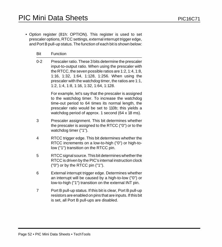
• Option register (81h: OPTION). This register is used to setprescaler options, RTCC settings, external interrupt trigger edge,and Port B pull-up status. The function of each bit is shown below:
Bit Function
0-2 Prescaler ratio. These 3 bits determine the prescalerinput-to-output ratio. When using the prescaler withthe RTCC, the seven possible ratios are 1:2, 1:4, 1:8,1:16, 1:32, 1:64, 1:128, 1:256. When using theprescaler with the watchdog timer, the ratios are 1:1,1:2, 1:4, 1:8, 1:16, 1:32, 1:64, 1:128.
For example, let's say that the prescaler is assignedto the watchdog timer. To increase the watchdogtime-out period to 64 times its normal length, theprescaler ratio would be set to 110b; this yields awatchdog period of approx. 1 second (64 x 18 ms).
3 Prescaler assignment. This bit determines whetherthe prescaler is assigned to the RTCC ("0") or to thewatchdog timer ("1").
4 RTCC trigger edge. This bit determines whether theRTCC increments on a low-to-high ("0") or high-to-low ("1") transition on the RTCC pin.
5 RTCC signal source. This bit determines whether theRTCC is driven by the PIC's internal instruction clock("0") or by the RTCC pin ("1").
6 External interrupt trigger edge. Determines whetheran interrupt will be caused by a high-to-low ("0") orlow-to-high ("1") transition on the external INT pin.
7 Port B pull-up status. If this bit is clear, Port B pull-upresistors are enabled on pins that are inputs. If this bitis set, all Port B pull-ups are disabled.
PIC16C71

TechTools • PIC Mini Data Sheets • Page 53
PIC Mini Data Sheets
DS
• Program Counter Low Byte (82h: PCL). Same as register 02h.
• Status Register (83h). Same as register 03h.
• File Select Register (84h: FSR). Same as register 04h.
• Data Direction Register for Port A (85h: TRISA). This is the datadirection register for Port A. In the Microchip data book, thisregister is referred to as “Tri-State A”, hence “TRISA” as anabbreviation.
Bits in this register which are set to “1” cause the correspondingbits in Port A to become inputs (the pins go into high impedancemode, allowing them to be driven by an external source). Bitswhich are cleared to “0” cause the corresponding bits in Port A tobecome outputs.
• Data Direction Register for Port B (86h: TRISB). This is the datadirection register for Port B.
Data direction registers in the PIC16C71 are addressable, unliketheir counterparts in PIC16C5x devices.
• A/D Control Register (88h: ADCON1). This register controls whichpins will be used as analog inputs and whether the A/D’s referencewill come from Vdd or from the external VREF pin. The bits thatcontrol these functions are shown below:
Bits 1,0 RA0 RA1 RA2 RA3 Ref.
0 0 analog analog analog analog Vdd0 1 analog analog analog ref. RA31 0 analog analog digital digital Vdd1 1 digital digital digital digital -
• A/D Conversion Result (89h: ADRES). Same as register 09h.
• Program Counter Latch High (8Ah). Same as register 0Ah.
• Interrupt Control Register (8Bh: INTCON). Same as register 0Bh.
PIC16C71

Page 54 • PIC Mini Data Sheets • TechTools
PIC Mini Data Sheets
PIC16C84
PIC16C84 Pin-OutThe following diagram shows the PIC16C84 pin-out:
Pin Function
RA0 - RA4 I/O Port ARB0 - RB7 I/O Port BINT External interrupt inputRTCC Real-time clock/counter inputMCLR Master clear (reset)OSC1 Oscillator inputOSC2/CLKOUT Oscillator output (OSC/4)Vdd Power supplyVss Ground
RA2
RA3
RA4/RTCC
MCLR
Vss
RB0/INT
RB1
RB2
RB3
RA1
RA0
OSC1
OSC2/CLKOUT
Vdd
RB7
RB6
RB5
RB4
1
2
3
4
5
6
7
8
9
18
17
16
15
14
13
12
11
10
PIC16C84
PDIPSOIC

TechTools • PIC Mini Data Sheets • Page 55
PIC Mini Data Sheets
DS
PIC16C84 MicrocontrollersThe table below shows the various PIC16C84’s available:
Part # Erasable Program Registers I/O Power Osc. Type Frequency
PIC16C84-04 Yes 1K x 14 100 x 8* 13 4.0 - 6.0 V RC,XTAL DC - 4 MHzPIC16C84-10 Yes 1K x 14 100 x 8* 13 4.0 - 6.0 V RC,XTAL DC - 10 MHz
PIC16LC84-04 Yes 1K x 14 100 x 8* 13 2.0 - 6.0 V RC,XTAL DC - 4 MHz
* 36 registers in RAM, 64 registers in EEPROM.
New and Modified FeaturesThe PIC16C84 shares many features with the older PIC16C5x andPIC16C71 devices. In fact, with a few notable exceptions, the ’84 is avirtual copy of the ’71. The following text describes the importantdifferences between the ’84 and the original ’5x series:
• 1K program space and 64 registers implemented in EEPROM.
• Interrupts possible from four sources: external pin, RTCC timer,EEPROM write complete, and change on four Port B pins.
• Port B modifications. Software controlled pull-up’s have beenadded, along with the ability to generate an interrupt when any offour pins changes state.
• 8-level hardware stack. Allows deeper nesting of subroutines.
• 14-bit instruction word. Provides larger page sizes for programmemory (2K) and RAM (128 bytes).
• New timers. Two new timers have been added to control delayson power-up and wake-up. These timers are the oscillator start-uptimer (OST) and power-up timer (PWRT).
• New I/O pin. An additional I/O pin has been added as bit 4 of PortA. This is physically implemented on pin 3 (RTCC/RA4).
• Status register changes. Program page select bits (bit 5-6) havebeen replaced by register page select bits.
PIC16C84

Page 56 • PIC Mini Data Sheets • TechTools
PIC Mini Data Sheets
• File select register changes. The FSR has been increased to 8bits, and bits 5-6 no longer function as register page select(register page selection is now done in the Status register).
• High byte added to PC. A high byte has been added to the programcounter to handle program memory paging.
• Page select bits removed. Program memory page select bits in theStatus register (PA0 - PA2) have been removed.
The part’s 1K of program space can be utilized without worryingabout page boundaries.
• Register 07h is unimplemented. This register cannot be used forstorage, as it can in 18-pin PIC16C5x devices.
• Reset vector moved to 0000h.
• Interrupt vector added at 0004h.
PIC16C84

TechTools • PIC Mini Data Sheets • Page 57
PIC Mini Data Sheets
DS
PIC16C84 RegistersThe following table shows the various registers in the PIC16C84; thefunction of each register is described in the following pages.
Register Function
- W register00h Indirect addressing register01h Real-time clock/counter (RTCC)02h Program counter low byte (PCL)- Stack registers (8)03h Status register04h File select register (FSR)05h I/O Port A06h I/O Port B07h Not implemented08h EEPROM data register (EEDATA)09h EEPROM address register (EEADR)0Ah Program counter latch high (PCLATH)0Bh Interrupt control register (INTCON)0Ch - 2Fh General purpose registers30h - 7Fh Not implemented
End of page 0 register memory
80h Indirect addressing register81h Option register82h Program counter low byte (PCL)83h Status register84h File select register (FSR)85h TRISA86h TRISB87h Not implemented88h EEPROM control register 1 (EECON1)89h EEPROM control register 2 (EECON2)8Ah Program counter latch high (PCLATH)8Bh Interrupt control register (INTCON)8Ch - AFh Reads/writes registers 0Ch - 2FhB0h - FFh Not implemented
PIC16C84
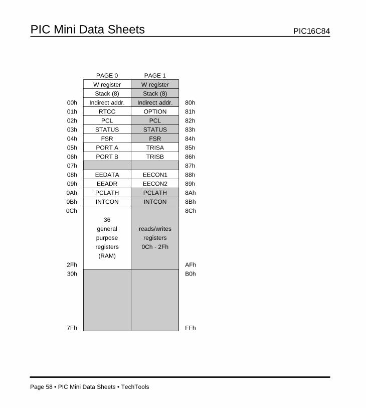
Page 58 • PIC Mini Data Sheets • TechTools
PIC Mini Data Sheets
PAGE 0
W register
Stack (8)
Indirect addr.
RTCC
PCL
STATUS
FSR
PORT A
PORT B
EEDATA
EEADR
PCLATH
INTCON
36
general
purpose
registers
(RAM)
PAGE 1
W register
Stack (8)
Indirect addr.
OPTION
PCL
STATUS
FSR
TRISA
TRISB
EECON1
EECON2
PCLATH
INTCON
reads/writes
registers
0Ch - 2Fh
00h
01h
02h
03h
04h
05h
06h
07h
08h
09h
0Ah
0Bh
0Ch
2Fh
30h
7Fh
80h
81h
82h
83h
84h
85h
86h
87h
88h
89h
8Ah
8Bh
8Ch
AFh
B0h
FFh
PIC16C84

TechTools • PIC Mini Data Sheets • Page 59
PIC Mini Data Sheets
DS
The following text describes the function of each new or modifiedregister. Refer to the PIC16C5x section for registers not shown here.
For some of the registers, you’ll notice the designation “xxh” following theregister name. This indicates the address of the register. Registers withno address cannot be addressed directly.
• Program Counter Low Byte (02h: PCL). The program counterholds the address for the instruction currently being executed. Theprogram counter and its associated eight-level stack are 13 bitswide, with PCL holding the lower 8 bits and PCH holding the upper5 bits. PCH is automatically loaded when a JMP or CALL isperformed. Although PCH is not addressable, your program canload PCH through the PCLATH register (see register f0A, later inthis section).
• Stack. The stack is comprised of eight registers which are used forcalling and returning from subroutines. The program counter ispushed onto the stack when a CALL is executed or an interrupt isacknowledged. The stack is popped in the event of a RET, RETW,or RETI instruction.
• Status Register (03h). This register contains the status of thearithmetic logic unit (ALU), the reset status, and the page selectbits for register memory (not program memory, as in PIC16C5xdevices).
The function of each bit in the status register is shown below:
Bit Function
0 Carry bit (C). Set if an addition or subtraction causesan overflow from the most significant bit of the result-ant (bit 7). Subtraction is included because it’s ex-ecuted by adding the two’s complement.
Also used by rotate instructions, which rotate thecontents of a register and copy the low or high orderbit of the register into the carry bit.
PIC16C84
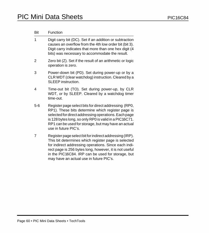
Page 60 • PIC Mini Data Sheets • TechTools
PIC Mini Data Sheets
Bit Function
1 Digit carry bit (DC). Set if an addition or subtractioncauses an overflow from the 4th low order bit (bit 3).Digit carry indicates that more than one hex digit (4bits) was necessary to accommodate the result.
2 Zero bit (Z). Set if the result of an arithmetic or logicoperation is zero.
3 Power-down bit (PD). Set during power-up or by aCLR WDT (clear watchdog) instruction. Cleared by aSLEEP instruction.
4 Time-out bit (TO). Set during power-up, by CLRWDT, or by SLEEP. Cleared by a watchdog timertime-out.
5-6 Register page select bits for direct addressing (RP0,RP1). These bits determine which register page isselected for direct addressing operations. Each pageis 128 bytes long, so only RP0 is valid in a PIC16C71.RP1 can be used for storage, but may have an actualuse in future PIC’s.
7 Register page select bit for indirect addressing (IRP).This bit determines which register page is selectedfor indirect addressing operations. Since each indi-rect page is 256 bytes long, however, it is not usefulin the PIC16C84. IRP can be used for storage, butmay have an actual use in future PIC’s.
PIC16C84

TechTools • PIC Mini Data Sheets • Page 61
PIC Mini Data Sheets
DS
The following table shows how various events affect thepower-down and time-out bits:
Event PD TO
Power-up 1 1Watchdog time-out x 0SLEEP instruction 0 1CLR WDT instruction 1 1
Lastly, this table shows the status of the power-down andtime-out bits after a reset:
Cause of Reset PD TO
Watchdog time-out (not during sleep) 1 0Watchdog time-out (during sleep) 0 0External reset (not during sleep) x xExternal reset (during sleep) 0 1Normal power-up 1 1
• File Select Register (04h: FSR). This register selects the registerfor indirect addressing. Bits 0-7 select 1 of 256 registers in thecurrent bank (the ’84 only has one bank). As described in thePIC16C5x register descriptions, a read or write to register 00h willaccess the register pointed to by the FSR.
• I/O Port A (05h). 5-bit I/O port. This register is used to read andwrite I/O Port A. It can be read and written just as any otherregister. However, read instructions always read the I/O pins,regardless of whether the pins are programmed as inputs oroutputs.
Bit 4 (pin 3) has an open-collector output and shares its pin withthe RTCC input.
PIC16C84

Page 62 • PIC Mini Data Sheets • TechTools
PIC Mini Data Sheets
• I/O Port B (06h). 8-bit I/O port. Each of the Port B pins has a weakinternal pull-up resistor (~250 µA). A pin’s pull-up is turned off if thepin is configured as an output, and a single bit in the Option registercan turn off all the pull-ups. The pull-up resistors are disabled onpower-on reset.
On bits 4-7 (pins 10-13), Port B has an interrupt on change featurethat can generate an interrupt if any of the pins changes state. Anypin configured as an output is excluded from the interrupt feature.
This interrupt can wake up the chip from sleep. Along with theinternal pull-ups, the interrupt from sleep feature makes it easy tointerface to a keypad and have wake-up on key press.
• EEPROM Data Register (08h: EEDATA). This register is used toread and write the 64 EEPROM registers.
• EEPROM Address Register (09h: EEADR). This register is usedto set the address of the EEPROM register that will be read orwritten.
• Program Counter Latch High (0Ah: PCLATH). This register isused to access the 5 high bits of the program counter (PCH).Unlike the lower 8 bits (PCL), the 5 high bits are not directlyaddresable. Instead, they are stored in PCLATH for later use.When the program counter is loaded with a new value during aJMP, CALL, or a write to PCL, the high bits are loaded fromPCLATH.
PIC16C84

TechTools • PIC Mini Data Sheets • Page 63
PIC Mini Data Sheets
DS
• Interrupt Control Register (0Bh: INTCON). This register is used toenable interrupts and to determine what caused an interrupt. Thefunction of each bit is given below:
Bit Function
0 Port B interrupt. This bit is set if an interrupt was theresult of a transition on any of the upper four bits ofPort B. It will remain set until cleared by software.
1 External interrupt. Set if an interrupt was caused by atransition on the external INT pin. Must be cleared bysoftware.
2 RTCC overflow interrupt. Set if an interrupt wascaused by an overflow in the real-time clock/counter.Must be cleared by software.
3 Port B interrupt enable. Determines whether the PortB interrupt is enabled (“1”) or disabled (“0”).
4 External interrupt enable. Determines whether theexternal interrupt is enabled (“1”) or disabled (“0”).
5 RTCC interrupt enable. Determines whether theRTCC interrupt is enabled (“1”) or disabled (“0”).
6 EEPROM interrupt enable. Determines whether theEEPROM write complete interrupt is enabled (“1”) ordisabled (“0”).
7 Global interrupt enable. Clearing this bit disables allinterrupts. Setting this bit allows all interrupts that areindividually enabled in bits 3-6.
• Indirect Addressing Register (80h). This register has the samefunction as register 00h.
PIC16C84

Page 64 • PIC Mini Data Sheets • TechTools
PIC Mini Data Sheets
• Option Register (81h: OPTION). This register is used to setprescaler options, RTCC settings, external interrupt trigger edge,and Port B pull-up status. The function of each bit is shown below:
Bit Function
0-2 Prescaler ratio. These 3 bits determine the prescalerinput-to-output ratio. When using the prescaler withthe RTCC, the seven possible ratios are 1:2, 1:4, 1:8,1:16, 1:32, 1:64, 1:128, 1:256. When using theprescaler with the watchdog timer, the ratios are 1:1,1:2, 1:4, 1:8, 1:16, 1:32, 1:64, 1:128.
For example, let's say that the prescaler is assignedto the watchdog timer. To increase the watchdogtime-out period to 64 times its normal length, theprescaler ratio would be set to 110b; this yields awatchdog period of approx. 1 second (64 x 18 ms).
3 Prescaler assignment. This bit determines whetherthe prescaler is assigned to the RTCC ("0") or to thewatchdog timer ("1").
4 RTCC trigger edge. This bit determines whether theRTCC increments on a low-to-high ("0") or high-to-low ("1") transition on the RTCC pin.
5 RTCC signal source. This bit determines whether theRTCC is driven by the PIC's internal instruction clock("0") or by the RTCC pin ("1").
6 External interrupt trigger edge. Determines whetheran interrupt will be caused by a high-to-low ("0") orlow-to-high ("1") transition on the external INT pin.
7 Port B pull-up status. If this bit is clear, Port B pull-upresistors are enabled on pins that are inputs. If this bitis set, all Port B pull-ups are disabled.
PIC16C84
TechTools • PIC Mini Data Sheets • Page 65
PIC Mini Data Sheets
DS
• Program Counter Low Byte (82h: PCL). Same as register 02h.
• Status Register (83h). Same as register 03h.
• File Select Register (84h: FSR). Same as register 04h.
• Data Direction Register for Port A (85h: TRISA). This is the datadirection register for Port A. In the Microchip data book, thisregister is referred to as “Tri-State A”, hence “TRISA” as anabbreviation.
Bits in this register which are set to “1” cause the correspondingbits in Port A to become inputs (the pins go into high impedancemode, allowing them to be driven by an external source). Bitswhich are cleared to “0” cause the corresponding bits in Port A tobecome outputs.
• Data Direction Register for Port B (86h: TRISB). This is the datadirection register for Port B.
Data direction registers in the PIC16C84 are addressable, unliketheir counterparts in PIC16C5x devices.
• EEPROM Control Register 1 (88h: EECON1). This register isused to control the reading and writing of the 64 EEPROMregisters. It’s also used to determine if the last write cycle wascompleted. The function of each bit is given below:
Bit Function
0 Read control bit. Setting this bit starts an EEPROMread cycle. The bit is automatically cleared after theread.
1 Write control bit. Setting this bit starts an EEPROMwrite cycle. The bit is automatically cleared after thewrite.
2 Write enable bit. If this bit is set, the EEPROM can bewritten; if it’s clear, the EEPROM can only be read.
PIC16C84

Page 66 • PIC Mini Data Sheets • TechTools
PIC Mini Data Sheets
Bit Function
3 Write error flag. This bit is automatically set if anEEPROM write cycle is prematurely terminated by anMCLR reset (during sleep or normal operation) or bya watchdog reset (during normal operation).
4 Write completion interrupt flag. Set when an EEPROMwrite cycle is completed. Must be cleared in software.Corresponding interrupt enable bit is in INTCONregister.
• EEPROM Control Register 2 (89h: EECON2). This register is notphysically implemented, and therefore cannot be read. However,EECON2 must be written to whenever an EEPROM write cycle isperformed. See the EEPROM read/write notes following theregister descriptions.
• Program Counter Latch High (8Ah). Same as register 0Ah.
• Interrupt Control Register (8Bh: INTCON). Same as register 0Bh.
Reading & Writing EEPROM RegistersSeparate from the PIC16C84’s 1K of program EEPROM space, thereexist 64 bytes of EEPROM that can be used by your program asnonvolatile data storage.
This memory is not mapped in the normal register space. Instead, it isaccessed through two registers: EEDATA (holds data to be read/written)and EEADR (holds address of EEPROM location). Additionally, twospecial registers control reading and writing of the EEPROM.
Reading from the EEPROM. To read an EEPROM location, yourprogram must write the address to the EEADR register and thenset bit 0 of EECON1 (read control bit). The desired data can beread from EEDATA in the next instruction. The following codeshows how to read the EEPROM:
PIC16C84

TechTools • PIC Mini Data Sheets • Page 67
PIC Mini Data Sheets
DS
mov EEADR,#00h ;Select first EEPROM locationsetb STATUS.5 ;Select register page 1setb EECON1.0 ;Start read cycleclrb STATUS.5 ;Select register page 0mov w,EEDATA ;Read data
Writing to the EEPROM. To write an EEPROM location, yourprogram must write the address to the EEADR register and thedata to the EEDATA register. Then your program must set bit 2 ofEECON1 (write enable), write a sequence of two bytes to EECON2,and then set bit 1 of EECON1 (write control bit). The writeoperation takes approximately 10 ms. The following code showshow to write the EEPROM:
mov EEADR,#00h ;Select first EEPROM locationmov EEDATA,#41h ;Store ASCII value for ‘A’setb STATUS.5 ;Select register page 1setb EECON1.2 ;Set write enable bitmov EECON2,#55h ;Write special byte #1mov EECON2,#AAh ;Write special byte #2setb EECON1.1 ;Start write cyclejb EECON1.1,$ ;Wait until write bit clearsclrb STATUS.5 ;Select register page 0
PIC16C84

Page 68 • PIC Mini Data Sheets • TechTools
PIC Mini Data Sheets