Embed Size (px)
Citation preview
PIC16(L)F1703/714/20-Pin 8-Bit Advanced Analog Flash Microcontrollers
Core Features
• C Compiler Optimized RISC Architecture• Only 49 Instructions• Operating Speed:
- 0-32 MHz- 125 ns minimum instruction cycle
• Interrupt Capability • 16-Level Deep Hardware Stack• Up to Two 8-Bit Timers• One 16-bit Timer• Power-on Reset (POR)• Power-up Timer (PWRT)• Low-Power Brown-out Reset (LPBOR)• Programmable Watchdog Timer (WDT) up to
256s• Programmable Code Protection
Memory
• Two Kwords Flash Program Memory• 256 Bytes Data SRAM Memory• Direct, Indirect and Relative Addressing modes• High-Endurance Flash Data Memory (HEF)
- 128 bytes of nonvolatile data storage- 100k erase/write cycles
Operating Characteristics
• Operating Voltage Range:- 1.8V to 3.6V (PIC16LF1703/7)- 2.3V to 5.5V (PIC16F1703/7)
• Temperature Range:- Industrial: -40°C to 85°C- Extended: -40°C to 125°C
Digital Peripherals
• Capture/Compare/PWM (CCP) module• Serial Communications:
- SPI, I2C• Up to 18 I/O Pins and One Input Pin:
- Individually programmable weak pull-ups- Slew rate control- Interrupt-on-change with edge-select
• Peripheral Pin Select (PPS):- Enables pin mapping of digital I/O
eXtreme Low-Power (XLP) Features
• Sleep mode: 50 nA @ 1.8V, typical• Watchdog Timer: 500 nA @ 1.8V, typical• Operating Current:
- 8 uA @ 32 kHz, 1.8V, typical- 32 uA/MHz @ 1.8V, typical
Intelligent Analog Peripherals
• Operational Amplifiers:- Two configurable rail-to-rail Op Amps- Selectable internal and external channels- 2 MHz gain bandwidth product
• 10-Bit Analog-to-Digital Converter (ADC):- Up to 12 external channels- Conversion available during Sleep- Temperature Indicator
• Zero-Cross Detector (ZCD):- Detect when AC signal on pin crosses
ground
Clocking Structure
• 16 MHz Internal Oscillator Block:- ±1% at calibration- Selectable frequency range from 0 to 32 MHz
• 31 kHz Low-Power Internal Oscillator
Programming/Debug Features
• In-Circuit Debug Integrated On-Chip• Emulation Header for Advanced Debug:
- Provides trace, background debug and up to 32 hardware break points
• In-Circuit Serial Programming™ (ICSP™) via Two Pins
2013-2015 Microchip Technology Inc. DS40001722C-page 1
PIC16(L)F1703/7
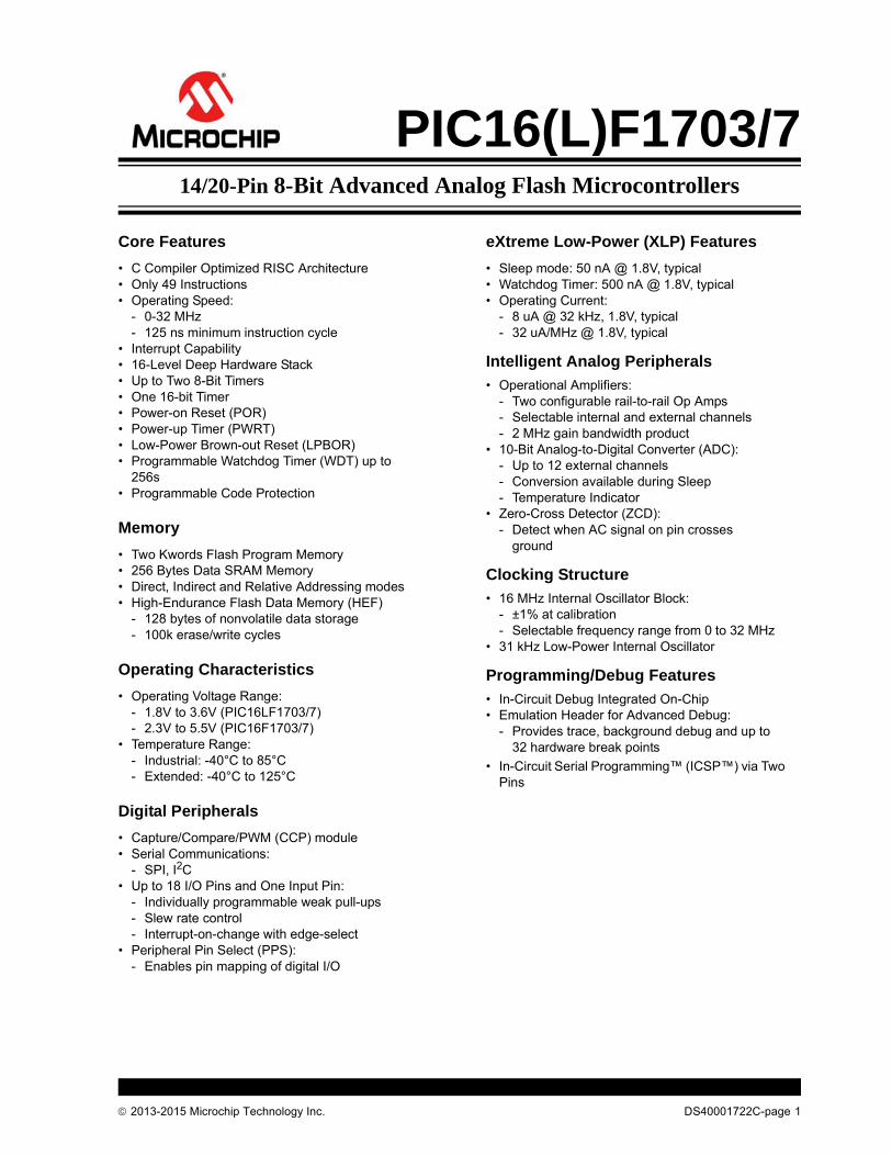
PIC16(L)F170x Family Types
Device
Da
ta S
he
et
Ind
ex
Pro
gra
m M
em
ory
Fla
sh
(w
ord
s)
Da
ta S
RA
M(b
yte
s)
Hig
h-E
nd
ura
nce
Fla
sh
(b
yte
s)
I/O
’s(2
)
10
-bit
AD
C (
ch
)
8-b
it D
AC
Hig
h-S
pee
d/
Co
mp
ara
tors
Op
Am
p
Zer
o C
ross
Tim
ers
(8/1
6-b
it)
CC
P
PW
M
CO
G
EU
SA
RT
MS
SP
(I2 C
/SP
I)
CL
C
PP
S
De
bu
g(1
)
XL
P
PIC16(L)F1703 (3) 2048 256 128 12 8 0 0 2 1 2/1 2 0 0 0 1 0 Y I/E Y
PIC16(L)F1704 (1) 4096 512 128 12 8 1 2 2 1 4/1 2 2 1 1 1 3 Y I/E Y
PIC16(L)F1705 (2) 8192 1024 128 12 8 1 2 2 1 4/1 2 2 1 1 1 3 Y I/E Y
PIC16(L)F1707 (3) 2048 256 128 18 12 0 0 2 1 2/1 2 0 0 0 1 0 Y I/E Y
PIC16(L)F1708 (1) 4096 512 128 18 12 1 2 2 1 4/1 2 2 1 1 1 3 Y I/E Y
PIC16(L)F1709 (2) 8192 1024 128 18 12 1 2 2 1 4/1 2 2 1 1 1 3 Y I/E Y
Note 1: Debugging Methods: (I) – Integrated on Chip; (H) – using Debug Header; E – using Emulation Header.2: One pin is input-only.
Data Sheet Index: (Unshaded devices are described in this document.)1: DS40001715 PIC16(L)F1704/8 Data Sheet, 14/20-Pin Flash, 8-bit Microcontrollers.2: DS40001729 PIC16(L)F1705/9 Data Sheet, 14/20-Pin Flash, 8-bit Microcontrollers.3: DS40001722 PIC16(L)F1703/7 Data Sheet, 14/20-Pin Flash, 8-bit Microcontrollers
Note: For other small form-factor package availability and marking information, please visithttp://www.microchip.com/packaging or contact your local sales office.
DS40001722C-page 2 2013-2015 Microchip Technology Inc.
PIC16(L)F1703/7
Pin Diagrams
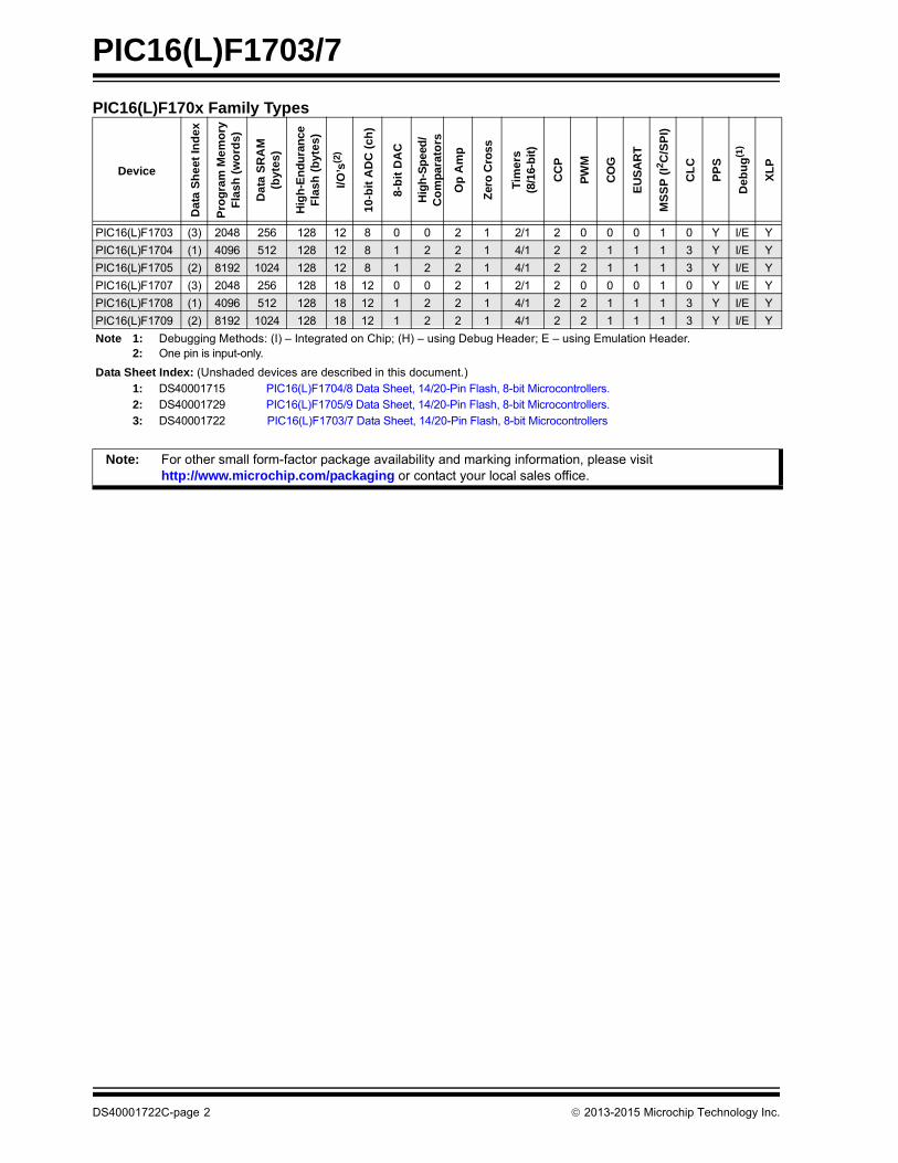
FIGURE 1: 14-PIN DIAGRAM FOR PIC16(L)F1703
FIGURE 2: 16-PIN PACKAGE DIAGRAM FOR PIC16(L)F1703
PDIP, SOIC, TSSOP
PIC
16
(L)F
17
03
1234567
VDD
RA5RA4
VPP/MCLR/RA3RC5RC4RC3
RA0/ICSPDATRA1/ICSPCLK
RA2
RC0RC1RC2
14
13121110
9
8
VSS
2
3
1
910
11
12
RC
4
4
VS
S
RA0/ICSPDATRA1/ICSPCLK
RA2RC0
NC
NC
VD
D
RA5RA4
RA3/MCLR/VPP
RC5
RC
3
RC
2
RC
1
6 75 8
15 1416 13
PIC16(L)F1703
QFN
2013-2015 Microchip Technology Inc. DS40001722C-page 3
PIC16(L)F1703/7
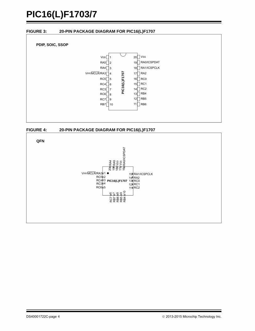
FIGURE 3: 20-PIN PACKAGE DIAGRAM FOR PIC16(L)F1707
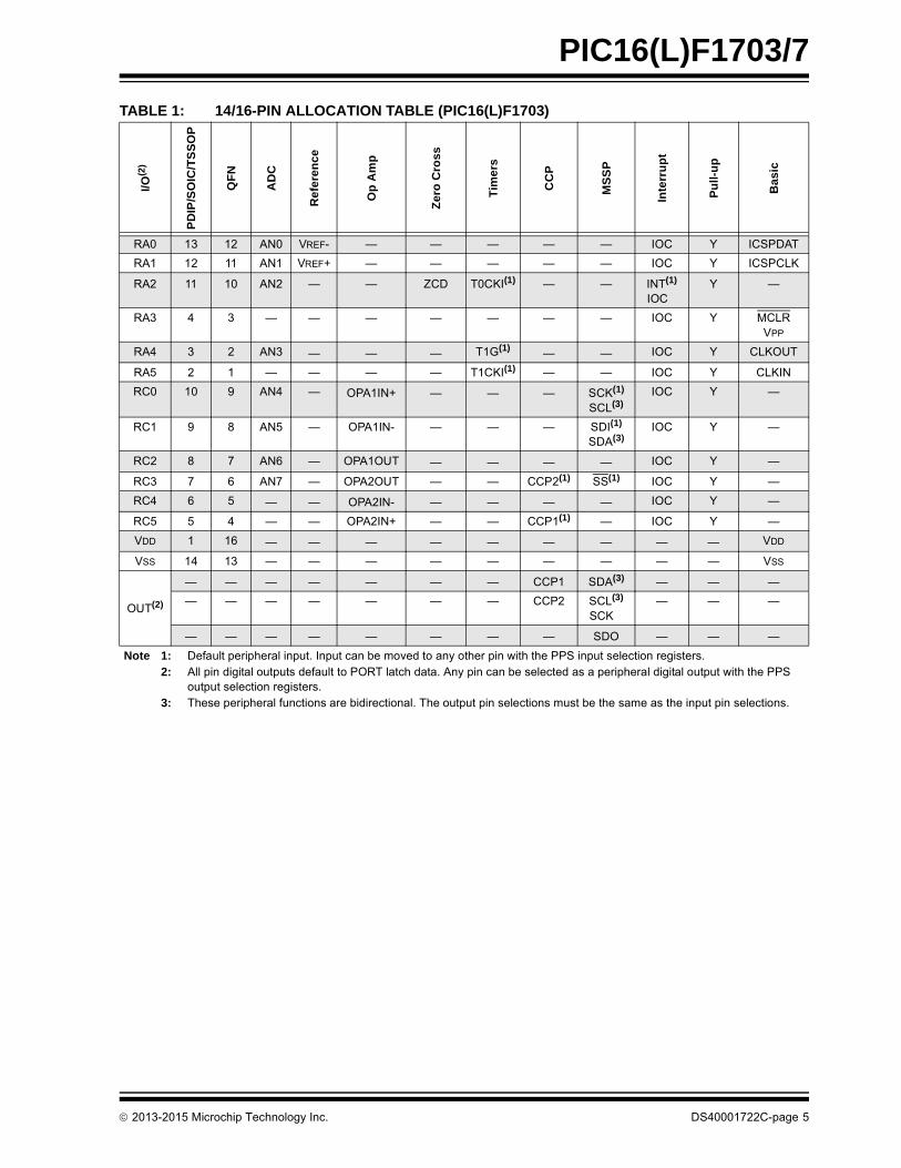
FIGURE 4: 20-PIN PACKAGE DIAGRAM FOR PIC16(L)F1707
PDIP, SOIC, SSOP
PIC
16
(L)F
17
07
2
3
4
5
6
7
8
9
10
VDD
RA5
RA4
VPP/MCLR/RA3
RC5
RC4
RC3
RC6
RC7
RB7
RA0/ICSPDAT
RA1/ICSPCLK
RA2
RC0
RC1
RC2
RB4
RB5
RB6
20
19
18
17
16
15
14
13
12
11
VSS1
QFN
2345
1
6 7 8 9
20 19
18 17
1610
12131415
11
PIC16(L)F1707
RB
4R
B5
RB
6R
B7
RC
7
VPP/MCLR/RA3RC5RC4RC3RC6
RA
4R
A5
VD
D
VS
S
RA
0/IC
SP
DA
T
RA1/ICSPCLKRA2RC0RC1RC2
DS40001722C-page 4 2013-2015 Microchip Technology Inc.
PIC16(L)F1703/7
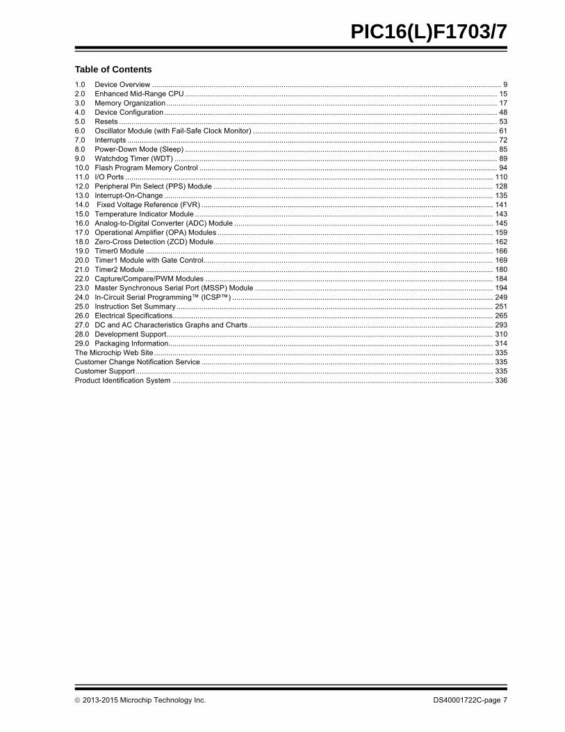
TABLE 1: 14/16-PIN ALLOCATION TABLE (PIC16(L)F1703)
I/O
(2)
PD
IP/S
OIC
/TS
SO
P
QF
N
AD
C
Re
fere
nc
e
Op
Am
p
Ze
ro C
ros
s
Tim
ers
CC
P
MS
SP
Inte
rru
pt
Pu
ll-u
p
Ba
sic
RA0 13 12 AN0 VREF- — — — — — IOC Y ICSPDAT
RA1 12 11 AN1 VREF+ — — — — — IOC Y ICSPCLK
RA2 11 10 AN2 — — ZCD T0CKI(1) — — INT(1)
IOCY —
RA3 4 3 — — — — — — — IOC Y MCLRVPP
RA4 3 2 AN3 — — — T1G(1) — — IOC Y CLKOUT
RA5 2 1 — — — — T1CKI(1) — — IOC Y CLKIN
RC0 10 9 AN4 — OPA1IN+ — — — SCK(1)
SCL(3)IOC Y —
RC1 9 8 AN5 — OPA1IN- — — — SDI(1)
SDA(3)IOC Y —
RC2 8 7 AN6 — OPA1OUT — — — — IOC Y —
RC3 7 6 AN7 — OPA2OUT — — CCP2(1) SS(1) IOC Y —
RC4 6 5 — — OPA2IN- — — — — IOC Y —
RC5 5 4 — — OPA2IN+ — — CCP1(1) — IOC Y —
VDD 1 16 — — — — — — — — — VDD
VSS 14 13 — — — — — — — — — VSS
OUT(2)
— — — — — — — CCP1 SDA(3) — — —
— — — — — — — CCP2 SCL(3)
SCK— — —
— — — — — — — — SDO — — —
Note 1: Default peripheral input. Input can be moved to any other pin with the PPS input selection registers. 2: All pin digital outputs default to PORT latch data. Any pin can be selected as a peripheral digital output with the PPS
output selection registers.3: These peripheral functions are bidirectional. The output pin selections must be the same as the input pin selections.
2013-2015 Microchip Technology Inc. DS40001722C-page 5

PIC16(L)F1703/7
TABLE 2: 20-PIN ALLOCATION TABLE (PIC16(L)F1707)I/
O(2
)
PD
IP/S
OIC
/S
SO
P
QF
N
AD
C
Re
fere
nc
e
Op
Am
p
Ze
ro C
ros
s
Tim
ers
CC
P
MS
SP
Inte
rru
pt
Pu
ll-u
p
Ba
sic
RA0 19 16 AN0 VREF- — — — — — IOC Y ICSPDAT
RA1 18 15 AN1 VREF+ — — — — — IOC Y ICSPCLK
RA2 17 14 AN2 — — ZCD T0CKI(1) — — INT(1)
IOCY —
RA3 4 1 — — — — — — — IOC Y MCLRVPP
RA4 3 20 AN3 — — — T1G(1) — — IOC Y CLKOUT
RA5 2 19 — — — — T1CKI — — IOC Y CLKIN
RB4 13 10 AN10 — OPA1IN- — — — SCK(1)
SDA(3)IOC Y —
RB5 12 9 AN11 — OPA1IN+ — — — — IOC Y —
RB6 11 8 — — — — — — SDI(1)
SCL(3)IOC Y —
RB7 10 7 — — — — — — — IOC Y —
RC0 16 13 AN4 — — — — — — IOC Y —
RC1 15 12 AN5 — — — — — — IOC Y —
RC2 14 11 AN6 — OPA1OUT — — — — IOC Y —
RC3 7 4 AN7 — OPA2OUT — — CCP2(1) — IOC Y —
RC4 6 3 — — — — — — — IOC Y —
RC5 5 2 — — — — — CCP1(1) — IOC Y —
RC6 8 5 AN8 — OPA2IN- — — — SS(1) IOC Y —
RC7 9 6 AN9 — OPA2IN+ — — — — IOC Y —
VDD 1 18 — — — — — — — — — VDD
VSS 20 17 — — — — — — — — — VSS
OUT(2)
— — — — — — — CPP1 SDA(3) — — —
— — — — — — — CPP2 SCL(3)
SCK— — —
— — — — — — — — SDO — — —
Note 1: Default peripheral input. Input can be moved to any other pin with the PPS input selection registers. 2: All pin digital outputs default to PORT latch data. Any pin can be selected as a peripheral digital output with the PPS
output selection registers.3: These peripheral functions are bidirectional. The output pin selections must be the same as the input pin selections.
DS40001722C-page 6 2013-2015 Microchip Technology Inc.
PIC16(L)F1703/7
Table of Contents
1.0 Device Overview .......................................................................................................................................................................... 92.0 Enhanced Mid-Range CPU ........................................................................................................................................................ 153.0 Memory Organization ................................................................................................................................................................. 174.0 Device Configuration .................................................................................................................................................................. 485.0 Resets ........................................................................................................................................................................................ 536.0 Oscillator Module (with Fail-Safe Clock Monitor) ....................................................................................................................... 617.0 Interrupts .................................................................................................................................................................................... 728.0 Power-Down Mode (Sleep) ........................................................................................................................................................ 859.0 Watchdog Timer (WDT) ............................................................................................................................................................. 8910.0 Flash Program Memory Control ................................................................................................................................................. 9411.0 I/O Ports ................................................................................................................................................................................... 11012.0 Peripheral Pin Select (PPS) Module ........................................................................................................................................ 12813.0 Interrupt-On-Change ................................................................................................................................................................ 13514.0 Fixed Voltage Reference (FVR) .............................................................................................................................................. 14115.0 Temperature Indicator Module ................................................................................................................................................. 14316.0 Analog-to-Digital Converter (ADC) Module .............................................................................................................................. 14517.0 Operational Amplifier (OPA) Modules ...................................................................................................................................... 15918.0 Zero-Cross Detection (ZCD) Module........................................................................................................................................ 16219.0 Timer0 Module ......................................................................................................................................................................... 16620.0 Timer1 Module with Gate Control............................................................................................................................................. 16921.0 Timer2 Module ......................................................................................................................................................................... 18022.0 Capture/Compare/PWM Modules ............................................................................................................................................ 18423.0 Master Synchronous Serial Port (MSSP) Module .................................................................................................................... 19424.0 In-Circuit Serial Programming™ (ICSP™) ............................................................................................................................... 24925.0 Instruction Set Summary .......................................................................................................................................................... 25126.0 Electrical Specifications............................................................................................................................................................ 26527.0 DC and AC Characteristics Graphs and Charts ....................................................................................................................... 29328.0 Development Support............................................................................................................................................................... 31029.0 Packaging Information.............................................................................................................................................................. 314The Microchip Web Site ..................................................................................................................................................................... 335Customer Change Notification Service .............................................................................................................................................. 335Customer Support .............................................................................................................................................................................. 335Product Identification System ............................................................................................................................................................ 336
2013-2015 Microchip Technology Inc. DS40001722C-page 7

PIC16(L)F1703/7
TO OUR VALUED CUSTOMERS
It is our intention to provide our valued customers with the best documentation possible to ensure successful use of your Microchipproducts. To this end, we will continue to improve our publications to better suit your needs. Our publications will be refined andenhanced as new volumes and updates are introduced.
If you have any questions or comments regarding this publication, please contact the Marketing Communications Department viaE-mail at [email protected]. We welcome your feedback.
Most Current Data Sheet
To obtain the most up-to-date version of this data sheet, please register at our Worldwide Web site at:
http://www.microchip.com
You can determine the version of a data sheet by examining its literature number found on the bottom outside corner of any page.The last character of the literature number is the version number, (e.g., DS30000000A is version A of document DS30000000).
Errata
An errata sheet, describing minor operational differences from the data sheet and recommended workarounds, may exist for currentdevices. As device/documentation issues become known to us, we will publish an errata sheet. The errata will specify the revisionof silicon and revision of document to which it applies.
To determine if an errata sheet exists for a particular device, please check with one of the following:
• Microchip’s Worldwide Web site; http://www.microchip.com• Your local Microchip sales office (see last page)When contacting a sales office, please specify which device, revision of silicon and data sheet (include literature number) you areusing.
Customer Notification System
Register on our web site at www.microchip.com to receive the most current information on all of our products.
DS40001722C-page 8 2013-2015 Microchip Technology Inc.
PIC16(L)F1703/7
1.0 DEVICE OVERVIEW
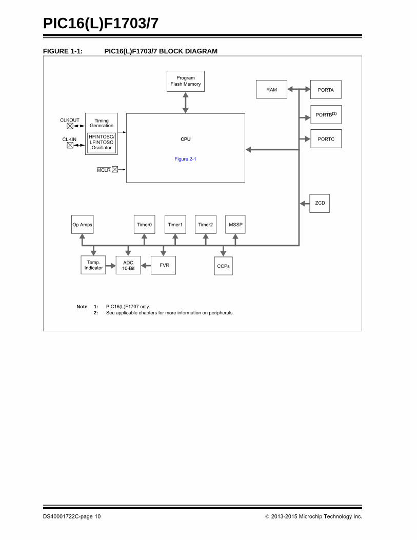
The PIC16(L)F1703/7 are described within this datasheet. They are available in 14-pin and 20-pin DIPpackages and 16-pin and 20-pin QFN packages.Figure 1-1 shows a block diagram of thePIC16(L)F1703/7 devices. Table 1-2 shows the pinoutdescriptions.
Reference Table 1-1 for peripherals available per device.
TABLE 1-1: DEVICE PERIPHERAL SUMMARY
Peripheral
PIC
16(L
)F17
03
PIC
16(L
)F17
07
Analog-to-Digital Converter (ADC) ● ●
Fixed Voltage Reference (FVR) ● ●
Zero-Cross Detection (ZCD) ● ●
Temperature Indicator ● ●
Capture/Compare/PWM (CCP/ECCP) Modules
CCP1 ● ●
CCP2 ● ●
Master Synchronous Serial Ports
MSSP ● ●
Op Amp
Op Amp 1 ● ●
Op Amp 2 ● ●
Timers
Timer0 ● ●
Timer1 ● ●
Timer2 ● ●
2013-2015 Microchip Technology Inc. DS40001722C-page 9
PIC16(L)F1703/7
FIGURE 1-1: PIC16(L)F1703/7 BLOCK DIAGRAM
PORTA
PORTB(1)
PORTC
Note 1: PIC16(L)F1707 only.2: See applicable chapters for more information on peripherals.
CPU
ProgramFlash Memory
RAM
TimingGeneration
LFINTOSCOscillator
MCLR
Figure 2-1
CLKIN
CLKOUT
ADC10-Bit
FVRTemp.
Indicator
MSSPTimer2Timer1Timer0
CCPs
Op Amps
HFINTOSC/
ZCD
DS40001722C-page 10 2013-2015 Microchip Technology Inc.
PIC16(L)F1703/7
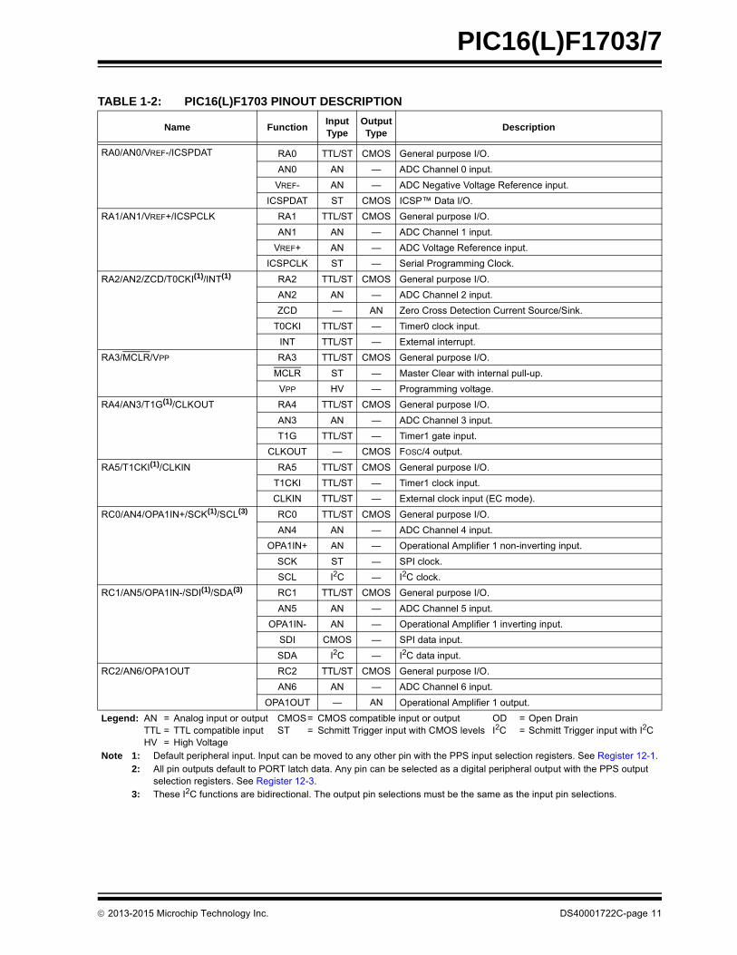
TABLE 1-2: PIC16(L)F1703 PINOUT DESCRIPTION
Name FunctionInput Type
Output Type
Description
RA0/AN0/VREF-/ICSPDAT RA0 TTL/ST CMOS General purpose I/O.
AN0 AN — ADC Channel 0 input.
VREF- AN — ADC Negative Voltage Reference input.
ICSPDAT ST CMOS ICSP™ Data I/O.
RA1/AN1/VREF+/ICSPCLK RA1 TTL/ST CMOS General purpose I/O.
AN1 AN — ADC Channel 1 input.
VREF+ AN — ADC Voltage Reference input.
ICSPCLK ST — Serial Programming Clock.
RA2/AN2/ZCD/T0CKI(1)/INT(1) RA2 TTL/ST CMOS General purpose I/O.
AN2 AN — ADC Channel 2 input.
ZCD — AN Zero Cross Detection Current Source/Sink.
T0CKI TTL/ST — Timer0 clock input.
INT TTL/ST — External interrupt.
RA3/MCLR/VPP RA3 TTL/ST CMOS General purpose I/O.
MCLR ST — Master Clear with internal pull-up.
VPP HV — Programming voltage.
RA4/AN3/T1G(1)/CLKOUT RA4 TTL/ST CMOS General purpose I/O.
AN3 AN — ADC Channel 3 input.
T1G TTL/ST — Timer1 gate input.
CLKOUT — CMOS FOSC/4 output.
RA5/T1CKI(1)/CLKIN RA5 TTL/ST CMOS General purpose I/O.
T1CKI TTL/ST — Timer1 clock input.
CLKIN TTL/ST — External clock input (EC mode).
RC0/AN4/OPA1IN+/SCK(1)/SCL(3) RC0 TTL/ST CMOS General purpose I/O.
AN4 AN — ADC Channel 4 input.
OPA1IN+ AN — Operational Amplifier 1 non-inverting input.
SCK ST — SPI clock.
SCL I2C — I2C clock.
RC1/AN5/OPA1IN-/SDI(1)/SDA(3) RC1 TTL/ST CMOS General purpose I/O.
AN5 AN — ADC Channel 5 input.
OPA1IN- AN — Operational Amplifier 1 inverting input.
SDI CMOS — SPI data input.
SDA I2C — I2C data input.
RC2/AN6/OPA1OUT RC2 TTL/ST CMOS General purpose I/O.
AN6 AN — ADC Channel 6 input.
OPA1OUT — AN Operational Amplifier 1 output.
Legend: AN = Analog input or output CMOS= CMOS compatible input or output OD = Open DrainTTL = TTL compatible input ST = Schmitt Trigger input with CMOS levels I2C = Schmitt Trigger input with I2C HV = High Voltage
Note 1: Default peripheral input. Input can be moved to any other pin with the PPS input selection registers. See Register 12-1.2: All pin outputs default to PORT latch data. Any pin can be selected as a digital peripheral output with the PPS output
selection registers. See Register 12-3.3: These I2C functions are bidirectional. The output pin selections must be the same as the input pin selections.
2013-2015 Microchip Technology Inc. DS40001722C-page 11
PIC16(L)F1703/7
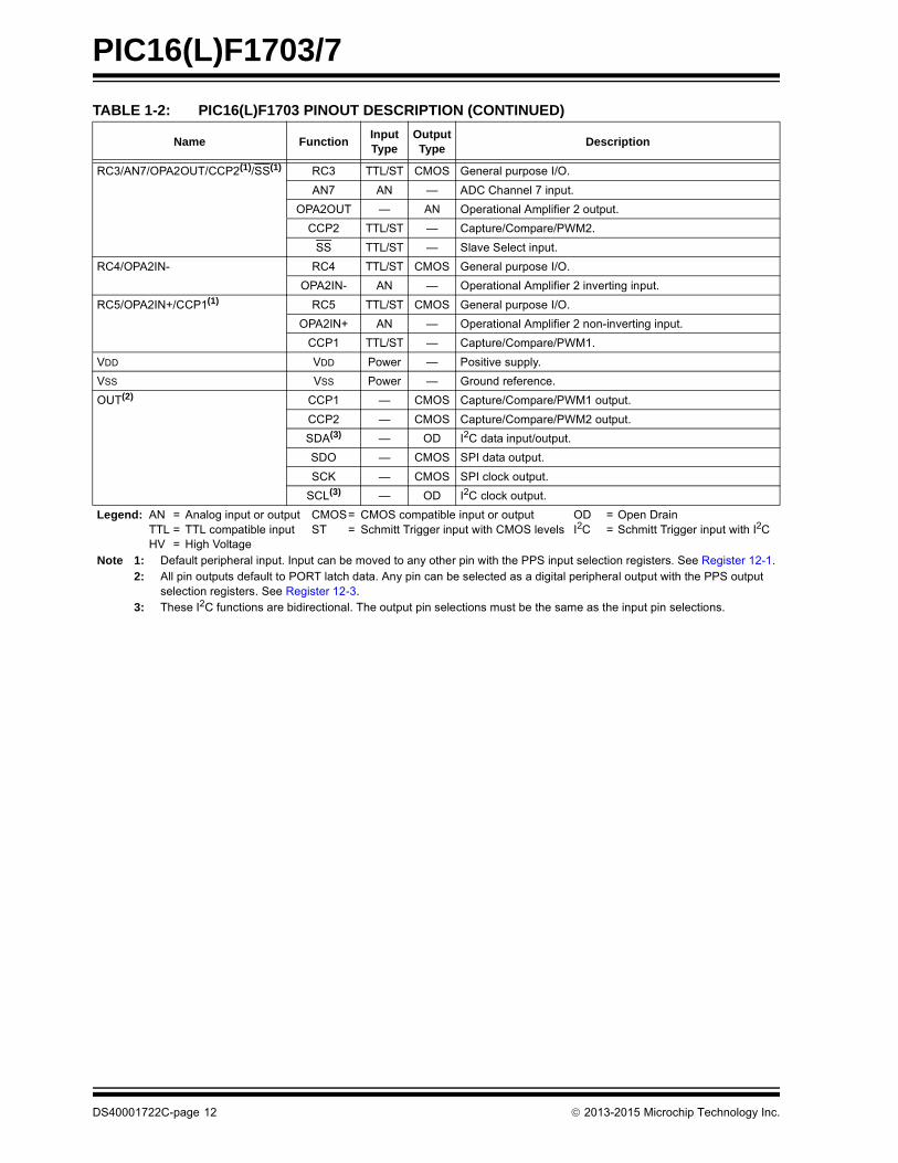
RC3/AN7/OPA2OUT/CCP2(1)/SS(1) RC3 TTL/ST CMOS General purpose I/O.
AN7 AN — ADC Channel 7 input.
OPA2OUT — AN Operational Amplifier 2 output.
CCP2 TTL/ST — Capture/Compare/PWM2.
SS TTL/ST — Slave Select input.
RC4/OPA2IN- RC4 TTL/ST CMOS General purpose I/O.
OPA2IN- AN — Operational Amplifier 2 inverting input.
RC5/OPA2IN+/CCP1(1) RC5 TTL/ST CMOS General purpose I/O.
OPA2IN+ AN — Operational Amplifier 2 non-inverting input.
CCP1 TTL/ST — Capture/Compare/PWM1.
VDD VDD Power — Positive supply.
VSS VSS Power — Ground reference.
OUT(2) CCP1 — CMOS Capture/Compare/PWM1 output.
CCP2 — CMOS Capture/Compare/PWM2 output.
SDA(3) — OD I2C data input/output.
SDO — CMOS SPI data output.
SCK — CMOS SPI clock output.
SCL(3) — OD I2C clock output.
TABLE 1-2: PIC16(L)F1703 PINOUT DESCRIPTION (CONTINUED)
Name FunctionInput Type
Output Type
Description
Legend: AN = Analog input or output CMOS= CMOS compatible input or output OD = Open DrainTTL = TTL compatible input ST = Schmitt Trigger input with CMOS levels I2C = Schmitt Trigger input with I2C HV = High Voltage
Note 1: Default peripheral input. Input can be moved to any other pin with the PPS input selection registers. See Register 12-1.2: All pin outputs default to PORT latch data. Any pin can be selected as a digital peripheral output with the PPS output
selection registers. See Register 12-3.3: These I2C functions are bidirectional. The output pin selections must be the same as the input pin selections.
DS40001722C-page 12 2013-2015 Microchip Technology Inc.

PIC16(L)F1703/7
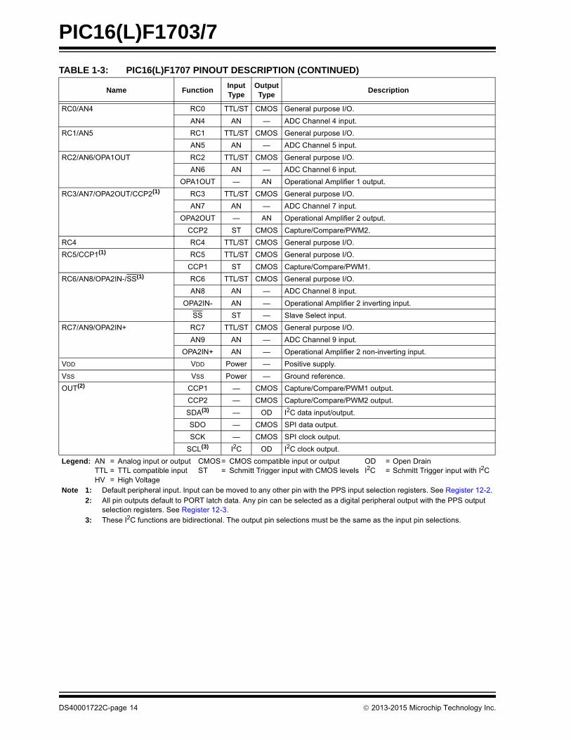
TABLE 1-3: PIC16(L)F1707 PINOUT DESCRIPTION
Name FunctionInput Type
Output Type
Description
RA0/AN0/VREF-/ICSPDAT RA0 TTL/ST CMOS General purpose I/O.
AN0 AN — ADC Channel 0 input.
VREF- AN — ADC Negative Voltage Reference input.
ICSPDAT ST CMOS ICSP™ Data I/O.
RA1/AN1/VREF+/ICSPCLK RA1 TTL/ST CMOS General purpose I/O.
AN1 AN — ADC Channel 1 input.
VREF+ AN — ADC Voltage Reference input.
ICSPCLK ST — Serial Programming Clock.
RA2/AN2/ZCD/T0CKI(1)/INT(1)
RA2 TTL/ST CMOS General purpose I/O.
AN2 AN — ADC Channel 2 input.
ZCD — AN Zero-Cross Detection Current Source/Sink.
T0CKI ST — Timer0 clock input.
INT ST — External interrupt.
RA3/MCLR/VPP RA3 TTL/ST CMOS General purpose I/O.
MCLR ST — Master Clear with internal pull-up.
VPP HV — Programming voltage.
RA4/AN3/T1G(1)/CLKOUT RA4 TTL/ST CMOS General purpose I/O.
AN3 AN — ADC Channel 3 input.
T1G ST — Timer1 gate input.
CLKOUT — CMOS FOSC/4 output.
RA5/T1CKI/CLKIN RA5 TTL/ST CMOS General purpose I/O.
T1CKI ST — Timer1 clock input.
CLKIN ST — External clock input (EC mode).
RB4/AN10/OPA1IN-/SCK(1)/SDA(3)
RB4 TTL/ST CMOS General purpose I/O.
AN10 AN — ADC Channel 10 input.
OPA1IN- AN — Operational Amplifier 1 inverting input.
SCK ST CMOS SPI clock.
SDA I2C OD I2C data input/output.
RB5/AN11/OPA1IN+ RB5 TTL/ST CMOS General purpose I/O.
AN11 AN — ADC Channel 11 input.
OPA1IN+ AN — Operational Amplifier 1 non-inverting input.
RB6/SDI(1)/SCL(3) RB6 TTL/ST CMOS General purpose I/O.
SDI CMOS — SPI data input.
SCL I2C OD I2C clock.
RB7 RB7 TTL/ST CMOS General purpose I/O.
Legend: AN = Analog input or output CMOS= CMOS compatible input or output OD = Open DrainTTL = TTL compatible input ST = Schmitt Trigger input with CMOS levels I2C = Schmitt Trigger input with I2C HV = High Voltage
Note 1: Default peripheral input. Input can be moved to any other pin with the PPS input selection registers. See Register 12-2.2: All pin outputs default to PORT latch data. Any pin can be selected as a digital peripheral output with the PPS output
selection registers. See Register 12-3.3: These I2C functions are bidirectional. The output pin selections must be the same as the input pin selections.
2013-2015 Microchip Technology Inc. DS40001722C-page 13
PIC16(L)F1703/7
RC0/AN4 RC0 TTL/ST CMOS General purpose I/O.
AN4 AN — ADC Channel 4 input.
RC1/AN5 RC1 TTL/ST CMOS General purpose I/O.
AN5 AN — ADC Channel 5 input.
RC2/AN6/OPA1OUT RC2 TTL/ST CMOS General purpose I/O.
AN6 AN — ADC Channel 6 input.
OPA1OUT — AN Operational Amplifier 1 output.
RC3/AN7/OPA2OUT/CCP2(1) RC3 TTL/ST CMOS General purpose I/O.
AN7 AN — ADC Channel 7 input.
OPA2OUT — AN Operational Amplifier 2 output.
CCP2 ST CMOS Capture/Compare/PWM2.
RC4 RC4 TTL/ST CMOS General purpose I/O.
RC5/CCP1(1) RC5 TTL/ST CMOS General purpose I/O.
CCP1 ST CMOS Capture/Compare/PWM1.
RC6/AN8/OPA2IN-/SS(1) RC6 TTL/ST CMOS General purpose I/O.
AN8 AN — ADC Channel 8 input.
OPA2IN- AN — Operational Amplifier 2 inverting input.
SS ST — Slave Select input.
RC7/AN9/OPA2IN+ RC7 TTL/ST CMOS General purpose I/O.
AN9 AN — ADC Channel 9 input.
OPA2IN+ AN — Operational Amplifier 2 non-inverting input.
VDD VDD Power — Positive supply.
VSS VSS Power — Ground reference.
OUT(2) CCP1 — CMOS Capture/Compare/PWM1 output.
CCP2 — CMOS Capture/Compare/PWM2 output.
SDA(3) — OD I2C data input/output.
SDO — CMOS SPI data output.
SCK — CMOS SPI clock output.
SCL(3) I2C OD I2C clock output.
TABLE 1-3: PIC16(L)F1707 PINOUT DESCRIPTION (CONTINUED)
Name FunctionInput Type
Output Type
Description
Legend: AN = Analog input or output CMOS= CMOS compatible input or output OD = Open DrainTTL = TTL compatible input ST = Schmitt Trigger input with CMOS levels I2C = Schmitt Trigger input with I2C HV = High Voltage
Note 1: Default peripheral input. Input can be moved to any other pin with the PPS input selection registers. See Register 12-2.2: All pin outputs default to PORT latch data. Any pin can be selected as a digital peripheral output with the PPS output
selection registers. See Register 12-3.3: These I2C functions are bidirectional. The output pin selections must be the same as the input pin selections.
DS40001722C-page 14 2013-2015 Microchip Technology Inc.

PIC16(L)F1703/7
2.0 ENHANCED MID-RANGE CPU
This family of devices contain an enhanced mid-range8-bit CPU core. The CPU has 49 instructions. Interruptcapability includes automatic context saving. Thehardware stack is 16 levels deep and has Overflow andUnderflow Reset capability. Direct, Indirect, and
Relative addressing modes are available. Two FileSelect Registers (FSRs) provide the ability to readprogram and data memory.
• Automatic Interrupt Context Saving
• 16-level Stack with Overflow and Underflow
• File Select Registers
• Instruction Set
FIGURE 2-1: CORE BLOCK DIAGRAM
Data Bus 8
14ProgramBus
Instruction reg
Program Counter
8 Level Stack(13-bit)
Direct Addr 7
12
Addr MUX
FSR reg
STATUS reg
MUX
ALU
Power-upTimer
OscillatorStart-up Timer
Power-onReset
WatchdogTimer
InstructionDecode &
Control
TimingGeneration
CLKIN
CLKOUT
VDD
8
8
Brown-outReset
12
3
VSS
InternalOscillator
Block
Data Bus 8
14ProgramBus
Instruction reg
Program Counter
8 Level Stack(13-bit)
Direct Addr 7
Addr MUX
FSR reg
STATUS reg
MUX
ALU
W reg
InstructionDecode &
Control
TimingGeneration
VDD
8
8
3
VSS
InternalOscillator
Block
15 Data Bus 8
14ProgramBus
Instruction Reg
Program Counter
16-Level Stack(15-bit)
Direct Addr 7
RAM Addr
Addr MUX
IndirectAddr
FSR0 Reg
STATUS Reg
MUX
ALU
InstructionDecode and
Control
TimingGeneration
VDD
8
8
3
VSS
InternalOscillator
Block
RAM
FSR regFSR regFSR1 Reg
15
15
MU
X
15
Program Memory
Read (PMR)
12
FSR regFSR regBSR Reg
5
ConfigurationConfigurationConfiguration
Flash
Program
Memory
2013-2015 Microchip Technology Inc. DS40001722C-page 15
PIC16(L)F1703/7
2.1 Automatic Interrupt Context Saving
During interrupts, certain registers are automaticallysaved in shadow registers and restored when returningfrom the interrupt. This saves stack space and usercode. See Section 7.5 “Automatic Context Saving”for more information.
2.2 16-Level Stack with Overflow and Underflow
These devices have a hardware stack memory 15 bitswide and 16 words deep. A Stack Overflow or Under-flow will set the appropriate bit (STKOVF or STKUNF)in the PCON register, and if enabled, will cause a soft-ware Reset. See Section 3.6 “Stack” for more details.
2.3 File Select Registers
There are two 16-bit File Select Registers (FSR). FSRscan access all file registers and program memory,which allows one Data Pointer for all memory. When anFSR points to program memory, there is one additionalinstruction cycle in instructions using INDF to allow thedata to be fetched. General purpose memory can nowalso be addressed linearly, providing the ability toaccess contiguous data larger than 80 bytes. There arealso new instructions to support the FSRs. SeeSection 3.7 “Indirect Addressing” for more details.
2.4 Instruction Set
There are 49 instructions for the enhanced mid-rangeCPU to support the features of the CPU. SeeSection 25.0 “Instruction Set Summary” for moredetails.
DS40001722C-page 16 2013-2015 Microchip Technology Inc.
PIC16(L)F1703/7
3.0 MEMORY ORGANIZATION
These devices contain the following types of memory:
• Program Memory
- Configuration Words
- Device ID
- User ID
- Flash Program Memory
• Data Memory
- Core Registers
- Special Function Registers
- General Purpose RAM
- Common RAM
The following features are associated with access andcontrol of program memory and data memory:
• PCL and PCLATH
• Stack
• Indirect Addressing
3.1 Program Memory Organization
The enhanced mid-range core has a 15-bit programcounter capable of addressing a 32K x 14 programmemory space. Table 3-1 shows the memory sizes
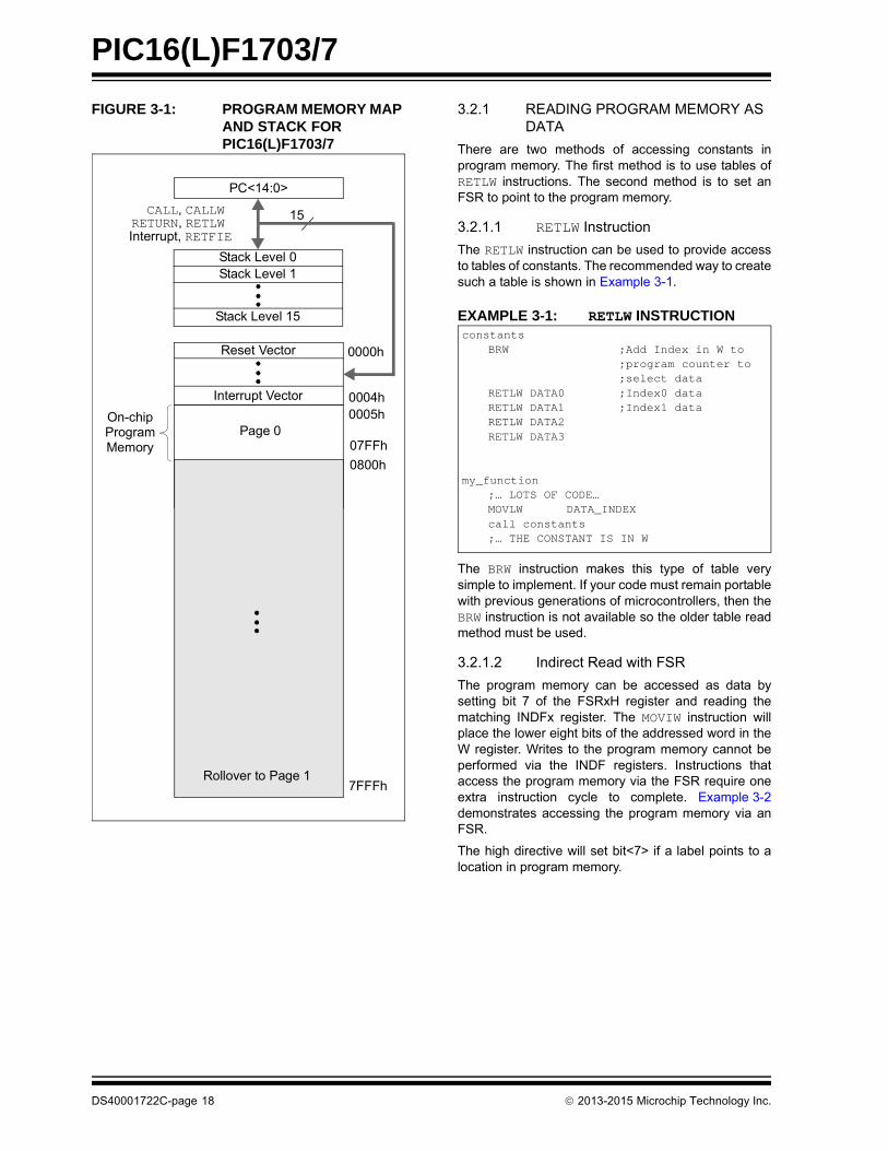
implemented for the PIC16(L)F1703/7 family. Accessinga location above these boundaries will cause awrap-around within the implemented memory space.The Reset vector is at 0000h and the interrupt vector isat 0004h (see Figure 3-1).
3.2 High-Endurance Flash
This device has a 128-byte section of high-enduranceProgram Flash Memory (PFM) in lieu of data EEPROM.This area is especially well suited for non-volatile datastorage that is expected to be updated frequently overthe life of the end product. See Section 10.2 “FlashProgram Memory Overview” for more information onwriting data to PFM. See Section 3.2.1.2 “IndirectRead with FSR” for more information about using theFSR registers to read byte data stored in PFM.
Note 1: The method to access Flash memorythrough the PMCON registers is describedin Section 10.0 “Flash Program MemoryControl”.
TABLE 3-1: DEVICE SIZES AND ADDRESSES
DeviceProgram Memory
Space (Words)Last Program Memory
AddressHigh-Endurance Flash
Memory Address Range (1)
PIC16(L)F1703/7 2,048 07FFh 0780h-07FFh
Note 1: High-endurance Flash applies to low byte of each address in the range.
2013-2015 Microchip Technology Inc. DS40001722C-page 17
PIC16(L)F1703/7
FIGURE 3-1: PROGRAM MEMORY MAP AND STACK FOR PIC16(L)F1703/7
3.2.1 READING PROGRAM MEMORY AS DATA
There are two methods of accessing constants inprogram memory. The first method is to use tables ofRETLW instructions. The second method is to set anFSR to point to the program memory.
3.2.1.1 RETLW Instruction
The RETLW instruction can be used to provide accessto tables of constants. The recommended way to createsuch a table is shown in Example 3-1.
EXAMPLE 3-1: RETLW INSTRUCTION
The BRW instruction makes this type of table verysimple to implement. If your code must remain portablewith previous generations of microcontrollers, then theBRW instruction is not available so the older table readmethod must be used.
3.2.1.2 Indirect Read with FSR
The program memory can be accessed as data bysetting bit 7 of the FSRxH register and reading thematching INDFx register. The MOVIW instruction willplace the lower eight bits of the addressed word in theW register. Writes to the program memory cannot beperformed via the INDF registers. Instructions thataccess the program memory via the FSR require oneextra instruction cycle to complete. Example 3-2demonstrates accessing the program memory via anFSR.
The high directive will set bit<7> if a label points to alocation in program memory.
PC<14:0>
15
0000h
0004h
Stack Level 0
Stack Level 15
Reset Vector
Interrupt Vector
CALL, CALLW RETURN, RETLW
Stack Level 1
0005hOn-chipProgramMemory
Page 007FFh
0800h
7FFFhRollover to Page 1
Interrupt, RETFIE
constantsBRW ;Add Index in W to
;program counter to;select data
RETLW DATA0 ;Index0 dataRETLW DATA1 ;Index1 dataRETLW DATA2RETLW DATA3
my_function;… LOTS OF CODE…MOVLW DATA_INDEXcall constants;… THE CONSTANT IS IN W
DS40001722C-page 18 2013-2015 Microchip Technology Inc.

PIC16(L)F1703/7
EXAMPLE 3-2: ACCESSING PROGRAM MEMORY VIA FSR
constantsRETLW DATA0 ;Index0 dataRETLW DATA1 ;Index1 dataRETLW DATA2RETLW DATA3
my_function;… LOTS OF CODE…MOVLW LOW constantsMOVWF FSR1LMOVLW HIGH constantsMOVWF FSR1HMOVIW 0[FSR1]
;THE PROGRAM MEMORY IS IN W
2013-2015 Microchip Technology Inc. DS40001722C-page 19
PIC16(L)F1703/7
3.3 Data Memory Organization
The data memory is partitioned in 32 memory bankswith 128 bytes in a bank. Each bank consists of(Figure 3-2):
• 12 core registers
• 20 Special Function Registers (SFR)
• Up to 80 bytes of General Purpose RAM (GPR)
• 16 bytes of common RAM
The active bank is selected by writing the bank numberinto the Bank Select Register (BSR). Unimplementedmemory will read as ‘0’. All data memory can beaccessed either directly (via instructions that use thefile registers) or indirectly via the two File SelectRegisters (FSR). See Section 3.7 “IndirectAddressing” for more information.
Data memory uses a 12-bit address. The upper five bitsof the address define the Bank address and the lowerseven bits select the registers/RAM in that bank.
3.3.1 CORE REGISTERS
The core registers contain the registers that directlyaffect the basic operation. The core registers occupythe first 12 addresses of every data memory bank(addresses x00h/x08h through x0Bh/x8Bh). Theseregisters are listed below in Table 3-2. For detailedinformation, see Table 3-9.
TABLE 3-2: CORE REGISTERS
Addresses BANKx
x00h or x80h INDF0x01h or x81h INDF1x02h or x82h PCLx03h or x83h STATUSx04h or x84h FSR0Lx05h or x85h FSR0Hx06h or x86h FSR1Lx07h or x87h FSR1Hx08h or x88h BSRx09h or x89h WREGx0Ah or x8Ah PCLATHx0Bh or x8Bh INTCON
DS40001722C-page 20 2013-2015 Microchip Technology Inc.
PIC16(L)F1703/7
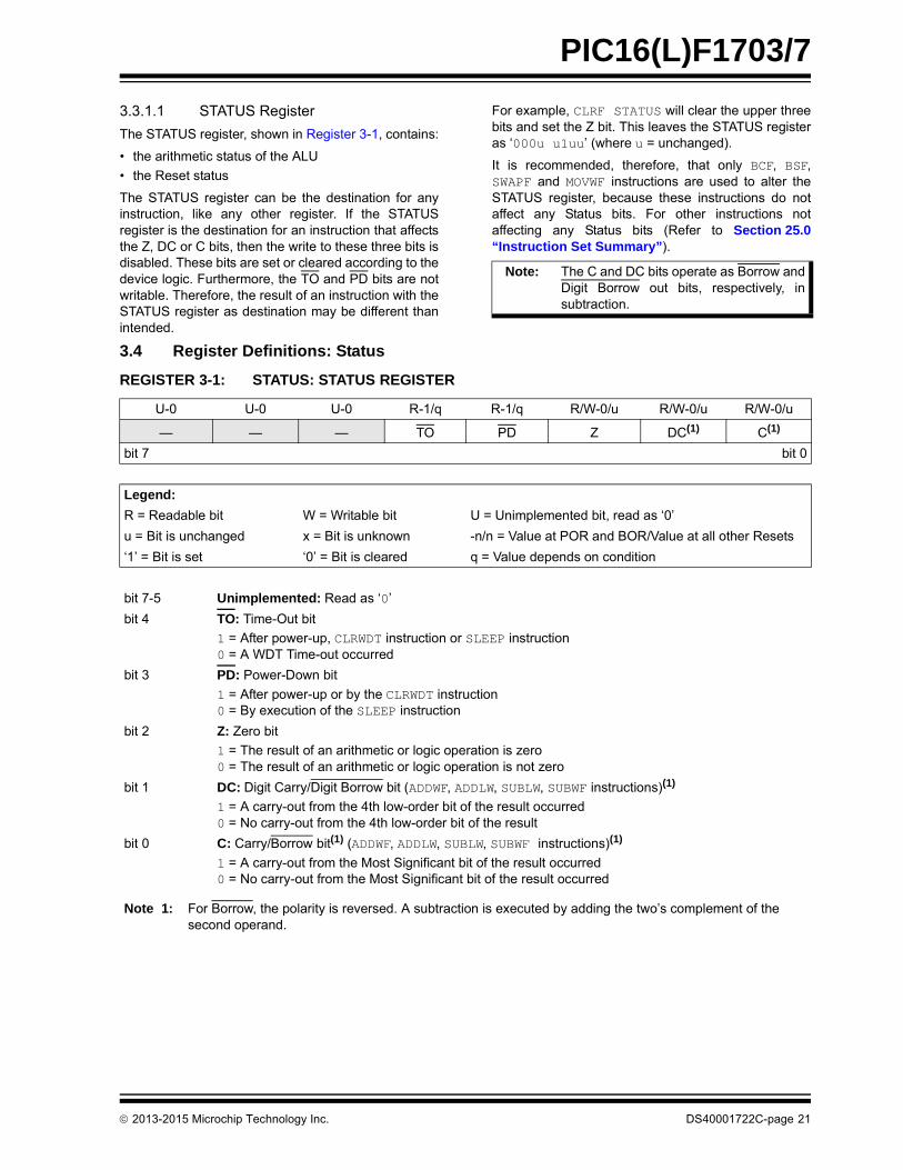
3.3.1.1 STATUS Register
The STATUS register, shown in Register 3-1, contains:
• the arithmetic status of the ALU
• the Reset status
The STATUS register can be the destination for anyinstruction, like any other register. If the STATUSregister is the destination for an instruction that affectsthe Z, DC or C bits, then the write to these three bits isdisabled. These bits are set or cleared according to thedevice logic. Furthermore, the TO and PD bits are notwritable. Therefore, the result of an instruction with theSTATUS register as destination may be different thanintended.
For example, CLRF STATUS will clear the upper threebits and set the Z bit. This leaves the STATUS registeras ‘000u u1uu’ (where u = unchanged).
It is recommended, therefore, that only BCF, BSF,SWAPF and MOVWF instructions are used to alter theSTATUS register, because these instructions do notaffect any Status bits. For other instructions notaffecting any Status bits (Refer to Section 25.0“Instruction Set Summary”).
3.4 Register Definitions: Status
Note: The C and DC bits operate as Borrow andDigit Borrow out bits, respectively, insubtraction.
REGISTER 3-1: STATUS: STATUS REGISTER
U-0 U-0 U-0 R-1/q R-1/q R/W-0/u R/W-0/u R/W-0/u
— — — TO PD Z DC(1) C(1)
bit 7 bit 0
Legend:
R = Readable bit W = Writable bit U = Unimplemented bit, read as ‘0’
u = Bit is unchanged x = Bit is unknown -n/n = Value at POR and BOR/Value at all other Resets
‘1’ = Bit is set ‘0’ = Bit is cleared q = Value depends on condition
bit 7-5 Unimplemented: Read as ‘0’
bit 4 TO: Time-Out bit
1 = After power-up, CLRWDT instruction or SLEEP instruction0 = A WDT Time-out occurred
bit 3 PD: Power-Down bit
1 = After power-up or by the CLRWDT instruction0 = By execution of the SLEEP instruction
bit 2 Z: Zero bit
1 = The result of an arithmetic or logic operation is zero0 = The result of an arithmetic or logic operation is not zero
bit 1 DC: Digit Carry/Digit Borrow bit (ADDWF, ADDLW, SUBLW, SUBWF instructions)(1)
1 = A carry-out from the 4th low-order bit of the result occurred0 = No carry-out from the 4th low-order bit of the result
bit 0 C: Carry/Borrow bit(1) (ADDWF, ADDLW, SUBLW, SUBWF instructions)(1)
1 = A carry-out from the Most Significant bit of the result occurred0 = No carry-out from the Most Significant bit of the result occurred
Note 1: For Borrow, the polarity is reversed. A subtraction is executed by adding the two’s complement of the second operand.
2013-2015 Microchip Technology Inc. DS40001722C-page 21

PIC16(L)F1703/7
3.4.1 SPECIAL FUNCTION REGISTER
The Special Function Registers are registers used bythe application to control the desired operation ofperipheral functions in the device. The Special FunctionRegisters occupy the 20 bytes after the core registers ofevery data memory bank (addresses x0Ch/x8Chthrough x1Fh/x9Fh). The registers associated with theoperation of the peripherals are described in theappropriate peripheral chapter of this data sheet.
3.4.2 GENERAL PURPOSE RAM
There are up to 80 bytes of GPR in each data memorybank. The Special Function Registers occupy the 20bytes after the core registers of every data memorybank (addresses x0Ch/x8Ch through x1Fh/x9Fh).
3.4.2.1 Linear Access to GPR
The general purpose RAM can be accessed in anon-banked method via the FSRs. This can simplifyaccess to large memory structures. See Section 3.7.2“Linear Data Memory” for more information.
3.4.3 COMMON RAM
There are 16 bytes of common RAM accessible from allbanks.
FIGURE 3-2: BANKED MEMORY PARTITIONING
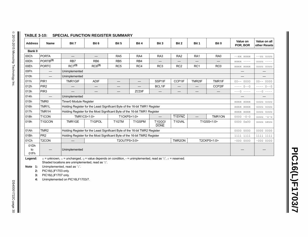
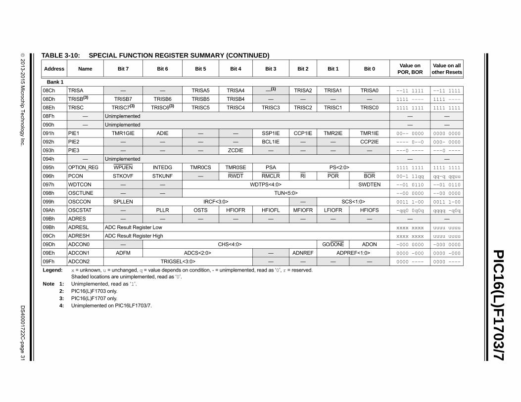
3.4.4 DEVICE MEMORY MAPS
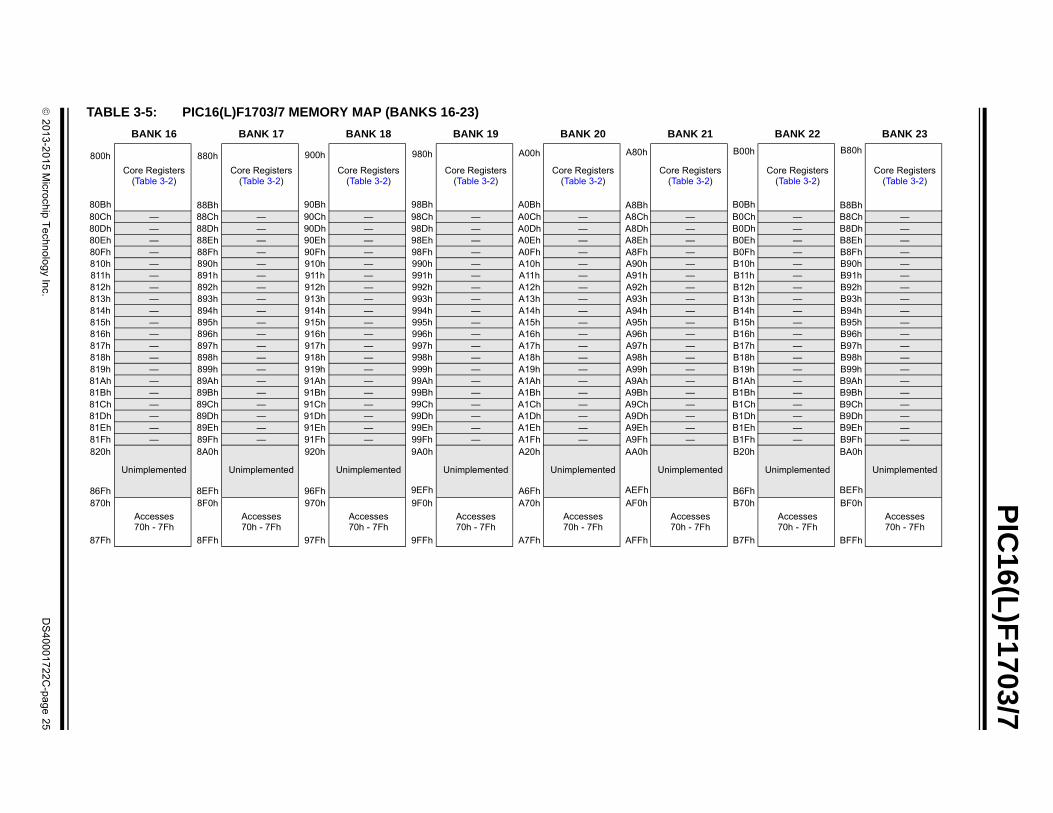
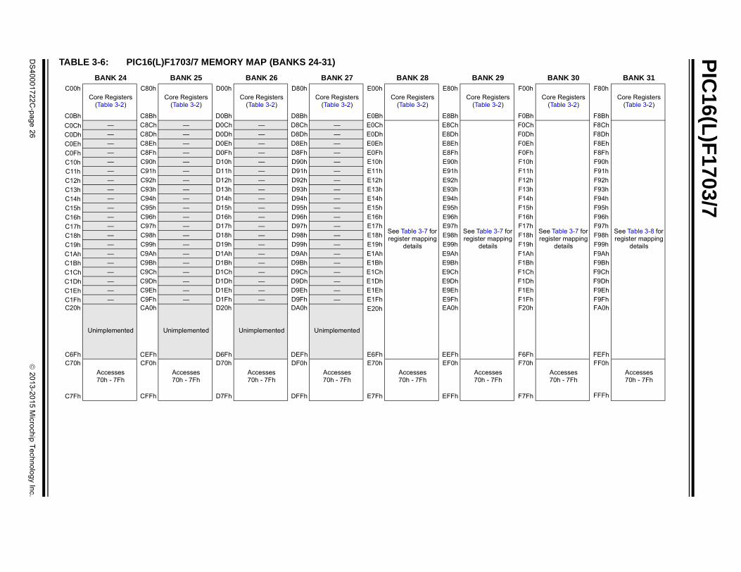
The memory maps for the device family are as shownin Tables 3-3 through 3-8.
0Bh0Ch
1Fh
20h
6Fh70h
7Fh
00h
Common RAM(16 bytes)
General Purpose RAM(80 bytes maximum)
Core Registers(12 bytes)
Special Function Registers(20 bytes maximum)
Memory Region7-bit Bank Offset
DS40001722C-page 22 2013-2015 Microchip Technology Inc.

2
01
3-2
01
5 M
icroch
ip T
ech
no
log
y Inc.
DS
40
00
17
22
C-p
ag
e 2
3
PIC
16(L)F
1703/7
TA
BANK 6 BANK 700 0h
Core Registers (Table 3-2)
380hCore Registers
(Table 3-2)
00 Bh 38Bh
00 Ch SLRCONA 38Ch INLVLA
00 Dh SLRCONB 38Dh INLVLB
00 Eh SLRCONC 38Eh INLVLC
00 Fh — 38Fh —
01 0h — 390h —
01 1h — 391h IOCAP
01 2h — 392h IOCAN
01 3h — 393h IOCAF
01 4h — 394h IOCBP
01 5h — 395h IOCBN
01 6h — 396h IOCBF
01 7h — 397h IOCCP
01 8h — 398h IOCCN
01 9h — 399h IOCCF
01 Ah — 39Ah —
01 Bh — 39Bh —
01 Ch — 39Ch —
01 Dh — 39Dh —
01 Eh — 39Eh —
01 Fh — 39Fh —
02 0h
Unimplemented
3A0h
Unimplemented
06 3EFhFh
07 0h
Accesses70h - 7Fh
3F0h
Accesses70h - 7Fh
07 Fh 3FFh
BLE 3-3: PIC16(L)F1703/7 MEMORY MAP (BANKS 0-7)
BANK 0 BANK 1 BANK 2 BANK 3 BANK 4 BANK 50h
Core Registers (Table 3-2)
080hCore Registers
(Table 3-2)
100hCore Registers
(Table 3-2)
180hCore Registers
(Table 3-2)
200hCore Registers
(Table 3-2)
280hCore Registers
(Table 3-2)
30
Bh 08Bh 10Bh 18Bh 20Bh 28Bh 30
Ch PORTA 08Ch TRISA 10Ch LATA 18Ch ANSELA 20Ch WPUA 28Ch ODCONA 30
Dh PORTB 08Dh TRISB 10Dh LATB 18Dh ANSELB 20Dh WPUB 28Dh ODCONB 30
Eh PORTC 08Eh TRISC 10Eh LATC 18Eh ANSELC 20Eh WPUC 28Eh ODCONC 30
Fh — 08Fh — 10Fh — 18Fh — 20Fh — 28Fh — 30
0h — 090h — 110h — 190h — 210h — 290h — 31
1h PIR1 091h PIE1 111h — 191h PMADR 211h SSP1BUF 291h CCPR1L 31
2h PIR2 092h PIE2 112h — 191h PMADRL 212h SSP1ADD 292h CCPR1H 31
3h PIR3 093h PIE3 113h — 192h PMADRH 213h SSP1MSK 293h CCP1CON 31
4h — 094h — 114h — 193h PMDATL 214h SSP1STAT 294h — 31
5h TMR0 095h OPTION_REG 115h — 194h PMDATH 215h SSP1CON1 295h — 31
6h TMR1L 096h PCON 116h BORCON 195h PMCON1 216h SSP1CON1 296h — 31
7h TMR1H 097h WDTCON 117h FVRCON 196h PMCON2 217h SSP1CON2 297h — 31
8h T1CON 098h OSCTUNE 118h — 197h — 218h SSP1CON3 298h CCPR2 31
9h T1GCON 099h OSCCON 119h — 198h — 219h — 298h CCPR2L 31
Ah TMR2 09Ah OSCSTAT 11Ah — 199h — 21Ah — 299h CCPR2H 31
Bh PR2 09Bh ADRESL 11Bh — 19Ah — 21Bh — 29Ah CCP2CON 31
Ch T2CON 09Ch ADRESH 11Ch ZCD1CON 19Bh — 21Ch — 29Bh — 31
Dh — 09Dh ADCON0 11Dh — 19Ch — 21Dh — 29Ch — 31
Eh — 09Eh ADCON1 11Eh — 19Dh — 21Eh — 29Dh — 31
Fh — 09Fh ADCON2 11Fh — 19Eh — 21Fh — 29Eh — 31
0h
General Purpose Register80 Bytes
0A0h
General Purpose Register80 Bytes
120h
General Purpose Register80 Bytes
19Fh — 220h
Unimplemented
29Fh — 321A0h
Unimplemented
2A0h
Unimplemented
Fh 0EFh 16Fh 1EFh 26Fh 2EFh 36
0hCommon RAM
70h - 7Fh
0F0hAccesses70h - 7Fh
170hAccesses70h - 7Fh
1F0hAccesses70h - 7Fh
270hAccesses70h - 7Fh
Accesses70h - 7Fh
37
2F0h
Fh 0FFh 17Fh 1FFh 27Fh 2FFh 37

PIC
16(L)F
1703/7
DS
40
00
17
22
C-p
ag
e 2
4
20
13
-20
15
Micro
chip
Te
chn
olo
gy In
c.
BANK 14 BANK 1500h
Core Registers (Table 3-2)
780hCore Registers
(Table 3-2)
0Bh 78Bh0Ch — 78Ch —0Dh — 78Dh —0Eh — 78Eh —0Fh — 78Fh —10h — 790h —11h — 791h —12h — 792h —13h — 793h —14h — 794h —15h — 795h —16h — 796h —17h — 797h —18h — 798h —19h — 799h —1Ah — 79Ah —1Bh — 79Bh —1Ch — 79Ch —1Dh — 79Dh —1Eh — 79Eh —1Fh — 79Fh —20h
Unimplemented
7A0h
Unimplemented
6Fh 7EFh70h
Accesses70h - 7Fh
7F0h
Accesses70h - 7Fh
7Fh 7FFh
TABLE 3-4: PIC16(L)F1703/7 MEMORY MAP (BANKS 8-15)BANK 8 BANK 9 BANK 10 BANK 11 BANK 12 BANK 13
400hCore Registers
(Table 3-2)
480hCore Registers
(Table 3-2)
500hCore Registers
(Table 3-2)
580hCore Registers
(Table 3-2)
600hCore Registers
(Table 3-2)
680hCore Registers
(Table 3-2)
7
40Bh 48Bh 50Bh 58Bh 60Bh 68Bh 740Ch — 48Ch — 50Ch — 58Ch — 60Ch — 68Ch — 740Dh — 48Dh — 50Dh — 58Dh — 60Dh — 68Dh — 740Eh — 48Eh — 50Eh — 58Eh — 60Eh — 68Eh — 740Fh — 48Fh — 50Fh — 58Fh — 60Fh — 68Fh — 7410h — 490h — 510h — 590h — 610h — 690h — 7411h — 491h — 511h OPA1CON 591h — 611h — 691h — 7412h — 492h — 512h — 592h — 612h — 692h — 7413h — 493h — 513h — 593h — 613h — 693h — 7414h — 494h — 514h — 594h — 614h — 694h — 7415h — 495h — 515h OPA2CON 595h — 615h — 695h — 7416h — 496h — 516h — 596h — 616h — 696h — 7417h — 497h — 517h — 597h — 617h — 697h — 7418h — 498h — 518h — 598h — 618h — 698h — 7419h — 499h — 519h — 599h — 619h — 699h — 741Ah — 49Ah — 51Ah — 59Ah — 61Ah — 69Ah — 741Bh — 49Bh — 51Bh — 59Bh — 61Bh — 69Bh — 741Ch — 49Ch — 51Ch — 59Ch — 61Ch — 69Ch — 741Dh — 49Dh — 51Dh — 59Dh — 61Dh — 69Dh — 741Eh — 49Eh — 51Eh — 59Eh 61Eh — 69Eh — 741Fh — 49Fh — 51Fh — 59Fh 61Fh — 69Fh — 7420h
Unimplemented
4A0h
Unimplemented
520h
Unimplemented
5A0h
Unimplemented
620h
Unimplemented
6A0h
Unimplemented
7
46Fh 4EFh 56Fh 5EFh 66Fh 6EFh 7470h
Accesses70h - 7Fh
4F0h
Accesses70h - 7Fh
570h
Accesses70h - 7Fh
5F0h
Accesses70h - 7Fh
670h
Accesses70h - 7Fh
6F0h
Accesses70h - 7Fh
7
47Fh 4FFh 57Fh 5FFh 67Fh 6FFh 7
2
01
3-2
01
5 M
icroch
ip T
ech
no
log
y Inc.
DS
40
00
17
22
C-p
ag
e 2
5
PIC
16(L)F
1703/7
TA
BANK 22 BANK 23
80
Core Registers (Table 3-2)
B80h
Core Registers (Table 3-2)
80 B8Bh80 — B8Ch —80 — B8Dh —80 — B8Eh —80 — B8Fh —81 — B90h —81 — B91h —81 — B92h —81 — B93h —81 — B94h —81 — B95h —81 — B96h —81 — B97h —81 — B98h —81 — B99h —81 — B9Ah —81 — B9Bh —81 — B9Ch —81 — B9Dh —81 — B9Eh —81 — B9Fh —82
Unimplemented
BA0h
Unimplemented
86 BEFh
87
Accesses70h - 7Fh
BF0h
Accesses70h - 7Fh
87 BFFh
BLE 3-5: PIC16(L)F1703/7 MEMORY MAP (BANKS 16-23)
BANK 16 BANK 17 BANK 18 BANK 19 BANK 20 BANK 21
0h
Core Registers (Table 3-2)
880h
Core Registers (Table 3-2)
900h
Core Registers (Table 3-2)
980h
Core Registers (Table 3-2)
A00h
Core Registers (Table 3-2)
A80h
Core Registers (Table 3-2)
B00h
Bh 88Bh 90Bh 98Bh A0Bh A8Bh B0BhCh — 88Ch — 90Ch — 98Ch — A0Ch — A8Ch — B0ChDh — 88Dh — 90Dh — 98Dh — A0Dh — A8Dh — B0DhEh — 88Eh — 90Eh — 98Eh — A0Eh — A8Eh — B0EhFh — 88Fh — 90Fh — 98Fh — A0Fh — A8Fh — B0Fh0h — 890h — 910h — 990h — A10h — A90h — B10h1h — 891h — 911h — 991h — A11h — A91h — B11h2h — 892h — 912h — 992h — A12h — A92h — B12h3h — 893h — 913h — 993h — A13h — A93h — B13h4h — 894h — 914h — 994h — A14h — A94h — B14h5h — 895h — 915h — 995h — A15h — A95h — B15h6h — 896h — 916h — 996h — A16h — A96h — B16h7h — 897h — 917h — 997h — A17h — A97h — B17h8h — 898h — 918h — 998h — A18h — A98h — B18h9h — 899h — 919h — 999h — A19h — A99h — B19hAh — 89Ah — 91Ah — 99Ah — A1Ah — A9Ah — B1AhBh — 89Bh — 91Bh — 99Bh — A1Bh — A9Bh — B1BhCh — 89Ch — 91Ch — 99Ch — A1Ch — A9Ch — B1ChDh — 89Dh — 91Dh — 99Dh — A1Dh — A9Dh — B1DhEh — 89Eh — 91Eh — 99Eh — A1Eh — A9Eh — B1EhFh — 89Fh — 91Fh — 99Fh — A1Fh — A9Fh — B1Fh0h
Unimplemented
8A0h
Unimplemented
920h
Unimplemented
9A0h
Unimplemented
A20h
Unimplemented
AA0h
Unimplemented
B20h
Fh 8EFh 96Fh 9EFh A6Fh AEFh B6Fh0h
Accesses70h - 7Fh
8F0h
Accesses70h - 7Fh
970h
Accesses70h - 7Fh
9F0h
Accesses70h - 7Fh
A70h
Accesses70h - 7Fh
AF0h
Accesses70h - 7Fh
B70h
Fh 8FFh 97Fh 9FFh A7Fh AFFh B7Fh
PIC
16(L)F
1703/7
DS
40
00
17
22
C-p
ag
e 2
6
20
13
-20
15
Micro
chip
Te
chn
olo
gy In
c.
BANK 30 BANK 3100h
Core Registers (Table 3-2)
F80hCore Registers
(Table 3-2)
0Bh F8Bh
0Ch
See Table 3-7 for register mapping
details
F8Ch
See Table 3-8 for register mapping
details
0Dh F8Dh
0Eh F8Eh
0Fh F8Fh
10h F90h
11h F91h
12h F92h
13h F93h
14h F94h
15h F95h
16h F96h
17h F97h
18h F98h
19h F99h
1Ah F9Ah
1Bh F9Bh
1Ch F9Ch
1Dh F9Dh
1Eh F9Eh
1Fh F9Fh20h FA0h
6Fh FEFh70h
Accesses70h - 7Fh
FF0h
Accesses70h - 7Fh
7Fh FFFh
TABLE 3-6: PIC16(L)F1703/7 MEMORY MAP (BANKS 24-31)
BANK 24 BANK 25 BANK 26 BANK 27 BANK 28 BANK 29C00h
Core Registers (Table 3-2)
C80hCore Registers
(Table 3-2)
D00hCore Registers
(Table 3-2)
D80hCore Registers
(Table 3-2)
E00hCore Registers
(Table 3-2)
E80hCore Registers
(Table 3-2)
F
C0Bh C8Bh D0Bh D8Bh E0Bh E8Bh F
C0Ch — C8Ch — D0Ch — D8Ch — E0Ch
See Table 3-7 for register mapping
details
E8Ch
See Table 3-7 for register mapping
details
F
C0Dh — C8Dh — D0Dh — D8Dh — E0Dh E8Dh F
C0Eh — C8Eh — D0Eh — D8Eh — E0Eh E8Eh F
C0Fh — C8Fh — D0Fh — D8Fh — E0Fh E8Fh F
C10h — C90h — D10h — D90h — E10h E90h F
C11h — C91h — D11h — D91h — E11h E91h F
C12h — C92h — D12h — D92h — E12h E92h F
C13h — C93h — D13h — D93h — E13h E93h F
C14h — C94h — D14h — D94h — E14h E94h F
C15h — C95h — D15h — D95h — E15h E95h F
C16h — C96h — D16h — D96h — E16h E96h F
C17h — C97h — D17h — D97h — E17h E97h F
C18h — C98h — D18h — D98h — E18h E98h F
C19h — C99h — D19h — D99h — E19h E99h F
C1Ah — C9Ah — D1Ah — D9Ah — E1Ah E9Ah F
C1Bh — C9Bh — D1Bh — D9Bh — E1Bh E9Bh F
C1Ch — C9Ch — D1Ch — D9Ch — E1Ch E9Ch F
C1Dh — C9Dh — D1Dh — D9Dh — E1Dh E9Dh F
C1Eh — C9Eh — D1Eh — D9Eh — E1Eh E9Eh F
C1Fh — C9Fh — D1Fh — D9Fh — E1Fh E9Fh FC20h
Unimplemented
CA0h
Unimplemented
D20h
Unimplemented
DA0h
Unimplemented
E20h EA0h F
C6Fh CEFh D6Fh DEFh E6Fh EEFh FC70h
Accesses70h - 7Fh
CF0h
Accesses70h - 7Fh
D70h
Accesses70h - 7Fh
DF0h
Accesses70h - 7Fh
E70h
Accesses70h - 7Fh
EF0h
Accesses70h - 7Fh
F
C7Fh CFFh D7Fh DFFh E7Fh EFFh F
PIC16(L)F1703/7
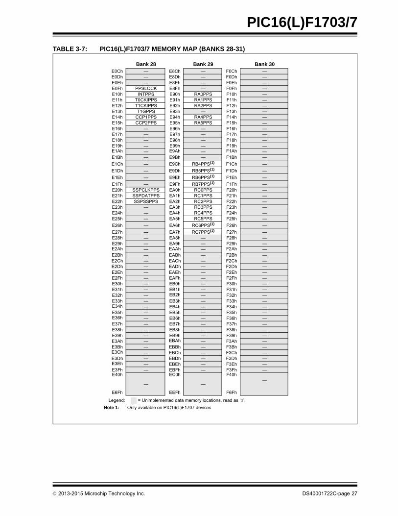
TABLE 3-7: PIC16(L)F1703/7 MEMORY MAP (BANKS 28-31)
Legend: = Unimplemented data memory locations, read as ‘0’,
Note 1: Only available on PIC16(L)F1707 devices
Bank 28 Bank 29 Bank 30E0Ch — E8Ch — F0Ch —E0Dh — E8Dh — F0Dh —E0Eh — E8Eh — F0Eh —E0Fh PPSLOCK E8Fh — F0Fh —E10h INTPPS E90h RA0PPS F10h —E11h T0CKIPPS E91h RA1PPS F11h —E12h T1CKIPPS E92h RA2PPS F12h —E13h T1GPPS E93h — F13h —E14h CCP1PPS E94h RA4PPS F14h —E15h CCP2PPS E95h RA5PPS F15h —E16h — E96h — F16h —E17h — E97h — F17h —E18h — E98h — F18h —E19h — E99h — F19h —E1Ah — E9Ah — F1Ah —E1Bh — E9Bh — F1Bh —
E1Ch — E9Ch RB4PPS(1) F1Ch —
E1Dh — E9Dh RB5PPS(1) F1Dh —
E1Eh — E9Eh RB6PPS(1) F1Eh —
E1Fh — E9Fh RB7PPS(1) F1Fh —E20h SSPCLKPPS EA0h RC0PPS F20h —E21h SSPDATPPS EA1h RC1PPS F21h —E22h SSPSSPPS EA2h RC2PPS F22h —E23h — EA3h RC3PPS F23h —E24h — EA4h RC4PPS F24h —E25h — EA5h RC5PPS F25h —
E26h — EA6h RC6PPS(1) F26h —
E27h — EA7h RC7PPS(1) F27h —E28h — EA8h — F28h —E29h — EA9h — F29h —E2Ah — EAAh — F2Ah —E2Bh — EABh — F2Bh —E2Ch — EACh — F2Ch —E2Dh — EADh — F2Dh —E2Eh — EAEh — F2Eh —E2Fh — EAFh — F2Fh —E30h — EB0h — F30h —E31h — EB1h — F31h —E32h — EB2h — F32h —E33h — EB3h — F33h —E34h — EB4h — F34h —E35h — EB5h — F35h —E36h — EB6h — F36h —E37h — EB7h — F37h —E38h — EB8h — F38h —E39h — EB9h — F39h —E3Ah — EBAh — F3Ah —E3Bh — EBBh — F3Bh —E3Ch — EBCh — F3Ch —E3Dh — EBDh — F3Dh —E3Eh — EBEh — F3Eh —E3Fh — EBFh — F3Fh —E40h
—
EC0h
—
F40h—
E6Fh EEFh F6Fh
2013-2015 Microchip Technology Inc. DS40001722C-page 27
PIC16(L)F1703/7
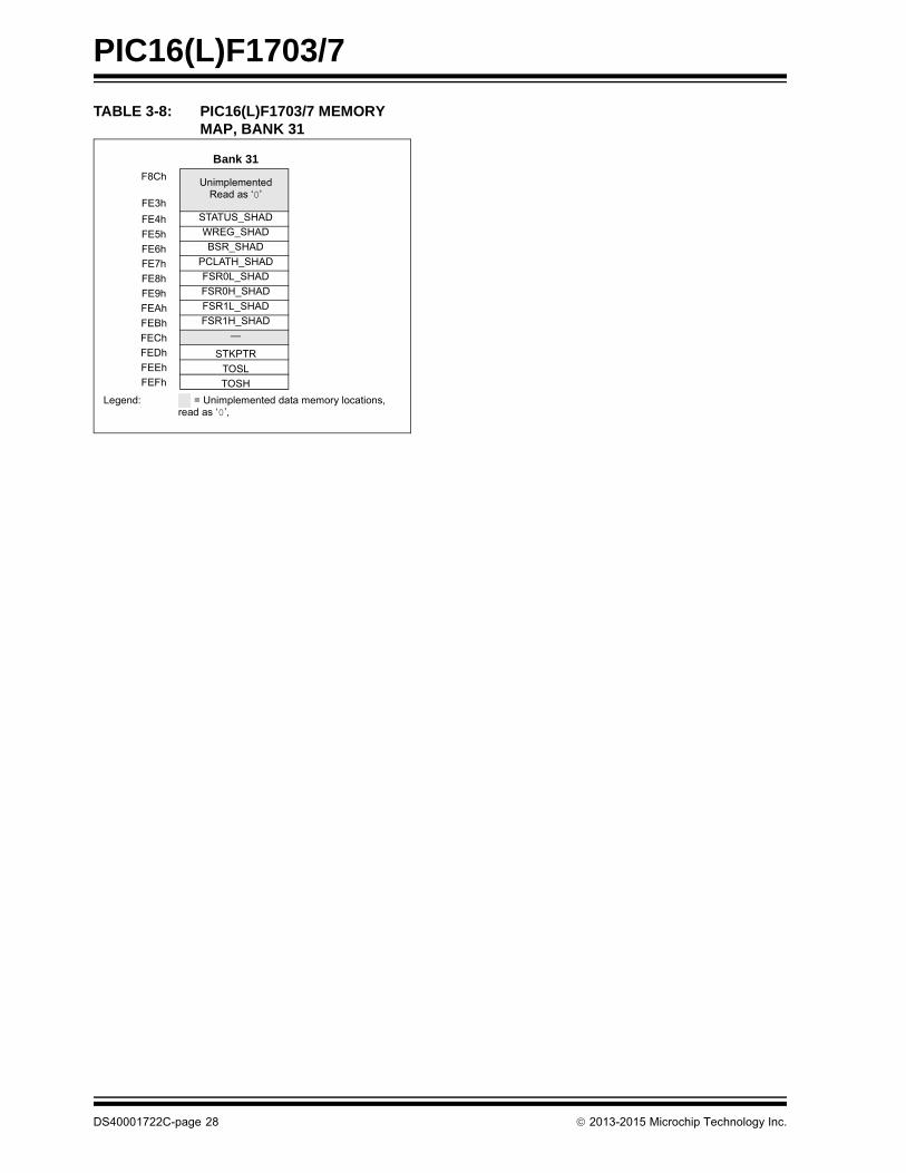
TABLE 3-8: PIC16(L)F1703/7 MEMORY MAP, BANK 31
Legend: = Unimplemented data memory locations, read as ‘0’,
Bank 31
F8ChUnimplemented
Read as ‘0’FE3h
FE4h STATUS_SHAD
FE5h WREG_SHAD
FE6h BSR_SHAD
FE7h PCLATH_SHAD
FE8h FSR0L_SHAD
FE9h FSR0H_SHAD
FEAh FSR1L_SHAD
FEBh FSR1H_SHAD
FECh —
FEDh STKPTRFEEh TOSLFEFh TOSH
DS40001722C-page 28 2013-2015 Microchip Technology Inc.
PIC16(L)F1703/7
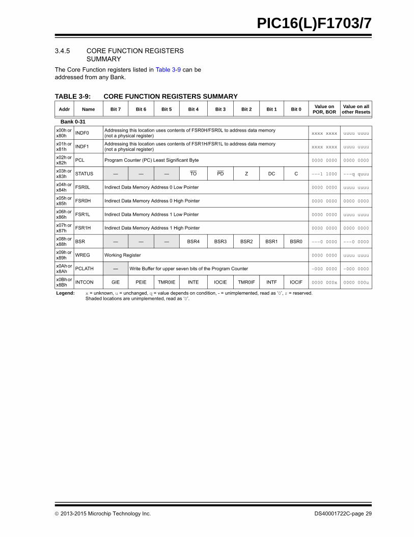
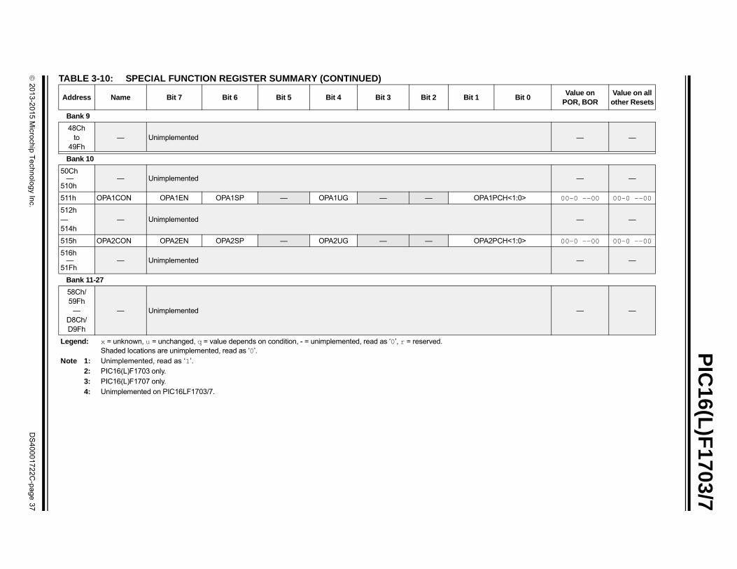
3.4.5 CORE FUNCTION REGISTERS SUMMARY
The Core Function registers listed in Table 3-9 can beaddressed from any Bank.
TABLE 3-9: CORE FUNCTION REGISTERS SUMMARY
Addr Name Bit 7 Bit 6 Bit 5 Bit 4 Bit 3 Bit 2 Bit 1 Bit 0Value on
POR, BORValue on all other Resets
Bank 0-31
x00h or x80h
INDF0Addressing this location uses contents of FSR0H/FSR0L to address data memory (not a physical register)
xxxx xxxx uuuu uuuu
x01h or x81h
INDF1Addressing this location uses contents of FSR1H/FSR1L to address data memory (not a physical register)
xxxx xxxx uuuu uuuu
x02h or x82h
PCL Program Counter (PC) Least Significant Byte 0000 0000 0000 0000
x03h or x83h
STATUS — — — TO PD Z DC C ---1 1000 ---q quuu
x04h or x84h
FSR0L Indirect Data Memory Address 0 Low Pointer 0000 0000 uuuu uuuu
x05h or x85h
FSR0H Indirect Data Memory Address 0 High Pointer 0000 0000 0000 0000
x06h or x86h
FSR1L Indirect Data Memory Address 1 Low Pointer 0000 0000 uuuu uuuu
x07h or x87h
FSR1H Indirect Data Memory Address 1 High Pointer 0000 0000 0000 0000
x08h or x88h
BSR — — — BSR4 BSR3 BSR2 BSR1 BSR0 ---0 0000 ---0 0000
x09h or x89h
WREG Working Register 0000 0000 uuuu uuuu
x0Ah or x8Ah
PCLATH — Write Buffer for upper seven bits of the Program Counter -000 0000 -000 0000
x0Bh or x8Bh
INTCON GIE PEIE TMR0IE INTE IOCIE TMR0IF INTF IOCIF 0000 000x 0000 000u
Legend: x = unknown, u = unchanged, q = value depends on condition, - = unimplemented, read as ‘0’, r = reserved. Shaded locations are unimplemented, read as ‘0’.
2013-2015 Microchip Technology Inc. DS40001722C-page 29
2
01
3-2
01
5 M
icroch
ip T
ech
no
log
y Inc.
DS
40
00
17
22
C-p
ag
e 3
0
PIC
16(L)F
1703/7
TA
A it 0Value on
POR, BORValue on all other Resets
B
00 A0 --xx xxxx --uu uuuu
00 xxxx ---- uuuu ----
00 C0 xxxx xxxx uuuu uuuu
00 — —
01 — —
01 R1IF 00-- 0000 00-- 0000
01 P2IF ---- 0--0 ---- 0--0
01 ---0 ---- ---0 ----
01 — —
01 xxxx xxxx uuuu uuuu
01 xxxx xxxx uuuu uuuu
01 xxxx xxxx uuuu uuuu
01 1ON 0000 -0-0 uuuu -u-u
01 0000 0x00 uuuu uxuu
01 0000 0000 0000 0000
01 1111 1111 1111 1111
01 -000 0000 -000 0000
— —
Le
No
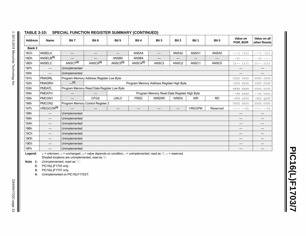
BLE 3-10: SPECIAL FUNCTION REGISTER SUMMARY
ddress Name Bit 7 Bit 6 Bit 5 Bit 4 Bit 3 Bit 2 Bit 1 B
ank 0
Ch PORTA — — RA5 RA4 RA3 RA2 RA1 R
Dh PORTB(3) RB7 RB6 RB5 RB4 — — — —
Eh PORTC RC7(3) RC6(3) RC5 RC4 RC3 RC2 RC1 R
Fh — Unimplemented
0h — Unimplemented
1h PIR1 TMR1GIF ADIF — — SSP1IF CCP1IF TMR2IF TM
2h PIR2 — — — — BCL1IF — — CC
3h PIR3 — — — ZCDIF — — — —
4h — Unimplemented
5h TMR0 Timer0 Module Register
6h TMR1L Holding Register for the Least Significant Byte of the 16-bit TMR1 Register
7h TMR1H Holding Register for the Most Significant Byte of the 16-bit TMR1 Register
8h T1CON TMR1CS<1:0> T1CKPS<1:0> — T1SYNC — TMR
9h T1GCON TMR1GE T1GPOL T1GTM T1GSPM T1GGO/DONE
T1GVAL T1GSS<1:0>
Ah TMR2 Holding Register for the Least Significant Byte of the 16-bit TMR2 Register
Bh PR2 Holding Register for the Most Significant Byte of the 16-bit TMR2 Register
Ch T2CON — T2OUTPS<3:0> TMR2ON T2CKPS<1:0>
01Dhto
01Fh— Unimplemented
gend: x = unknown, u = unchanged, q = value depends on condition, - = unimplemented, read as ‘0’, r = reserved. Shaded locations are unimplemented, read as ‘0’.
te 1: Unimplemented, read as ‘1’.2: PIC16(L)F1703 only.3: PIC16(L)F1707 only.4: Unimplemented on PIC16LF1703/7.
2
01
3-2
01
5 M
icroch
ip T
ech
no
log
y Inc.
DS
40
00
17
22
C-p
ag
e 3
1
PIC
16(L)F
1703/7
B
08 ISA0 --11 1111 --11 1111
08 1111 ---- 1111 ----
08 ISC0 1111 1111 1111 1111
08 — —
09 — —
09 R1IE 00-- 0000 0000 0000
09 P2IE ---- 0--0 000- 0000
09 ---0 ---- ---0 ----
09 — —
09 1111 1111 1111 1111
09 OR 00-1 11qq qq-q qquu
09 TEN --01 0110 --01 0110
09 --00 0000 --00 0000
09 0011 1-00 0011 1-00
09 OFS -qq0 0q0q qqqq -q0q
09 — —
09 xxxx xxxx uuuu uuuu
09 xxxx xxxx uuuu uuuu
09 ON -000 0000 -000 0000
09 0000 -000 0000 -000
09 0000 ---- 0000 ----
TA
A it 0Value on
POR, BORValue on all other Resets
Le
No
ank 1
Ch TRISA — — TRISA5 TRISA4 —(1) TRISA2 TRISA1 TR
Dh TRISB(3) TRISB7 TRISB6 TRISB5 TRISB4 — — — —
Eh TRISC TRISC7(3) TRISC6(3) TRISC5 TRISC4 TRISC3 TRISC2 TRISC1 TR
Fh — Unimplemented
0h — Unimplemented
1h PIE1 TMR1GIE ADIE — — SSP1IE CCP1IE TMR2IE TM
2h PIE2 — — — — BCL1IE — — CC
3h PIE3 — — — ZCDIE — — — —
4h — Unimplemented
5h OPTION_REG WPUEN INTEDG TMR0CS TMR0SE PSA PS<2:0>
6h PCON STKOVF STKUNF — RWDT RMCLR RI POR B
7h WDTCON — — WDTPS<4:0> SWD
8h OSCTUNE — — TUN<5:0>
9h OSCCON SPLLEN IRCF<3:0> — SCS<1:0>
Ah OSCSTAT — PLLR OSTS HFIOFR HFIOFL MFIOFR LFIOFR HFI
Bh ADRES — — — — — — — —
Bh ADRESL ADC Result Register Low
Ch ADRESH ADC Result Register High
Dh ADCON0 — CHS<4:0> GO/DONE AD
Eh ADCON1 ADFM ADCS<2:0> — ADNREF ADPREF<1:0>
Fh ADCON2 TRIGSEL<3:0> — — — —
BLE 3-10: SPECIAL FUNCTION REGISTER SUMMARY (CONTINUED)
ddress Name Bit 7 Bit 6 Bit 5 Bit 4 Bit 3 Bit 2 Bit 1 B
gend: x = unknown, u = unchanged, q = value depends on condition, - = unimplemented, read as ‘0’, r = reserved. Shaded locations are unimplemented, read as ‘0’.
te 1: Unimplemented, read as ‘1’.2: PIC16(L)F1703 only.3: PIC16(L)F1707 only.4: Unimplemented on PIC16LF1703/7.

PIC
16(L)F
1703/7
DS
40
00
17
22
C-p
ag
e 3
2
20
13
-20
15
Micro
chip
Te
chn
olo
gy In
c.
TA0 --xx -xxx --uu -uuu
— xxxx ---- uuuu ----
TC0 xxxx xxxx uuuu uuuu
— —
— —
— —
— —
— —
— —
— —
RDY 10-- ---q uu-- ---u
0q00 0000 0q00 0000
— —
— —
— —
— —
1INTN 0-x0 --00 0-x0 --00
— —
— —
— —
it 0Value on
POR, BORValue on all other Resets
Bank 2
10Ch LATA — — LATA5 LATA4 — LATA2 LATA1 LA
10Dh LATB(3) LATB7 LATB6 LATB5 LATB4 — — —
10Eh LATC LATC7(3) LATC6(3) LATC5 LATC4 LATC3 LATC2 LATC1 LA
10Fh — Unimplemented
110h — Unimplemented
111h — Unimplemented
112h — Unimplemented
113h — Unimplemented
114h — Unimplemented
115h — Unimplemented
116h BORCON SBOREN BORFS — — — — — BOR
117h FVRCON FVREN FVRRDY TSEN TSRNG CDAFVR<1:0> ADFVR<1:0>
118h — Unimplemented
119h — Unimplemented
11Ah — Unimplemented
11Bh — Unimplemented
11Ch ZCD1CON ZCD1EN — ZCD1OUT ZCD1POL — — ZCD1INTP ZCD
11Dh — Unimplemented
11Eh — Unimplemented
11Fh — Unimplemented
TABLE 3-10: SPECIAL FUNCTION REGISTER SUMMARY (CONTINUED)
Address Name Bit 7 Bit 6 Bit 5 Bit 4 Bit 3 Bit 2 Bit 1 B
Legend: x = unknown, u = unchanged, q = value depends on condition, - = unimplemented, read as ‘0’, r = reserved. Shaded locations are unimplemented, read as ‘0’.
Note 1: Unimplemented, read as ‘1’.2: PIC16(L)F1703 only.3: PIC16(L)F1707 only.4: Unimplemented on PIC16LF1703/7.
2
01
3-2
01
5 M
icroch
ip T
ech
no
log
y Inc.
DS
40
00
17
22
C-p
ag
e 3
3
PIC
16(L)F
1703/7
B
18 SA0 ---1 -111 ---1 -111
18 --11 ---- --11 ----
18 SC0 11-- 1111 11-- 1111
18 — —
19 — —
19 0000 0000 0000 0000
19 1000 0000 1000 0000
19 xxxx xxxx uuuu uuuu
19 --xx xxxx --uu uuuu
19 D -000 x000 -000 q000
19 0000 0000 0000 0000
19 erved ---- --01 ---- --01
19 — —
19 — —
19 — —
19 — —
19 — —
19 — —
19 — —
19 — —
TA
A it 0Value on
POR, BORValue on all other Resets
Le
No
ank 3
Ch ANSELA — — — ANSA4 — ANSA2 ANSA1 AN
Dh ANSELB(3) — — ANSB5 ANSB4 — — — —
Eh ANSELC ANSC7(3) ANSC6(3) ANSC5(2) ANSC4(2) ANSC3 ANSC2 ANSC1 AN
Fh — Unimplemented
0h — Unimplemented
1h PMADRL Program Memory Address Register Low Byte
2h PMADRH —(1) Program Memory Address Register High Byte
3h PMDATL Program Memory Read Data Register Low Byte
4h PMDATH — — Program Memory Read Data Register High Byte
5h PMCON1 — CFGS LWLO FREE WRERR WREN WR R
6h PMCON2 Program Memory Control Register 2
7h VREGCON(4) — — — — — — VREGPM Res
8h — Unimplemented
9h — Unimplemented
Ah — Unimplemented
Bh — Unimplemented
Ch — Unimplemented
Dh — Unimplemented
Eh — Unimplemented
Fh — Unimplemented
BLE 3-10: SPECIAL FUNCTION REGISTER SUMMARY (CONTINUED)
ddress Name Bit 7 Bit 6 Bit 5 Bit 4 Bit 3 Bit 2 Bit 1 B
gend: x = unknown, u = unchanged, q = value depends on condition, - = unimplemented, read as ‘0’, r = reserved. Shaded locations are unimplemented, read as ‘0’.
te 1: Unimplemented, read as ‘1’.2: PIC16(L)F1703 only.3: PIC16(L)F1707 only.4: Unimplemented on PIC16LF1703/7.
PIC
16(L)F
1703/7
DS
40
00
17
22
C-p
ag
e 3
4
20
13
-20
15
Micro
chip
Te
chn
olo
gy In
c.
UA0 --11 1111 --11 1111
— 1111 ---- 1111 ----
UC0 1111 1111 1111 1111
— —
— —
xxxx xxxx uuuu uuuu
xxxx xxxx uuuu uuuu
xxxx xxxx uuuu uuuu
F 0000 0000 0000 0000
0000 0000 0000 0000
EN 0000 0000 0000 0000
EN 0000 0000 0000 0000
— —
it 0Value on
POR, BORValue on all other Resets
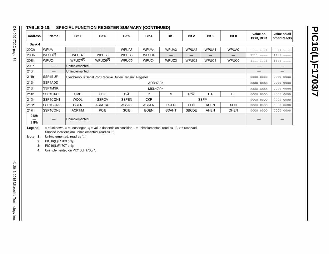
Bank 4
20Ch WPUA — — WPUA5 WPUA4 WPUA3 WPUA2 WPUA1 WP
20Dh WPUB(3) WPUB7 WPUB6 WPUB5 WPUB4 — — —
20Eh WPUC WPUC7(3) WPUC6(3) WPUC5 WPUC4 WPUC3 WPUC2 WPUC1 WP
20Fh — Unimplemented
210h — Unimplemented
211h SSP1BUF Synchronous Serial Port Receive Buffer/Transmit Register
212h SSP1ADD ADD<7:0>
213h SSP1MSK MSK<7:0>
214h SSP1STAT SMP CKE D/A P S R/W UA B
215h SSP1CON1 WCOL SSPOV SSPEN CKP SSPM
216h SSP1CON2 GCEN ACKSTAT ACKDT ACKEN RCEN PEN RSEN S
217h SSP1CON3 ACKTIM PCIE SCIE BOEN SDAHT SBCDE AHEN DH
218h—
21Fh— Unimplemented
TABLE 3-10: SPECIAL FUNCTION REGISTER SUMMARY (CONTINUED)
Address Name Bit 7 Bit 6 Bit 5 Bit 4 Bit 3 Bit 2 Bit 1 B
Legend: x = unknown, u = unchanged, q = value depends on condition, - = unimplemented, read as ‘0’, r = reserved. Shaded locations are unimplemented, read as ‘0’.
Note 1: Unimplemented, read as ‘1’.2: PIC16(L)F1703 only.3: PIC16(L)F1707 only.4: Unimplemented on PIC16LF1703/7.
2
01
3-2
01
5 M
icroch
ip T
ech
no
log
y Inc.
DS
40
00
17
22
C-p
ag
e 3
5
PIC
16(L)F
1703/7
B
28 A0 --00 -000 --00 -000
28 0000 ---- 0000 ----
28 C0 0000 0000 0000 0000
28 — —
29 — —
29 xxxx xxxx uuuu uuuu
29 xxxx xxxx uuuu uuuu
29 --00 0000 --00 0000
— —
29 xxxx xxxx uuuu uuuu
29 xxxx xxxx uuuu uuuu
29 --00 0000 --00 0000
— —
TA
A it 0Value on
POR, BORValue on all other Resets
Le
No
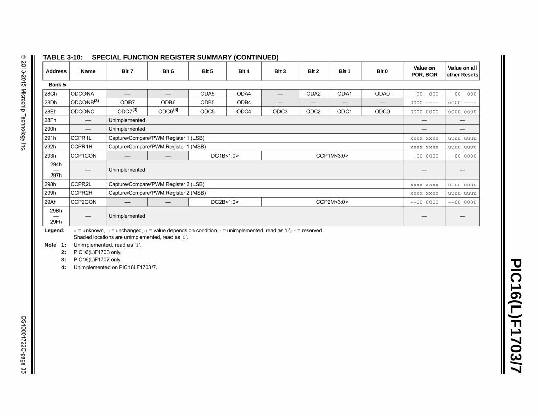
ank 5
Ch ODCONA — — ODA5 ODA4 — ODA2 ODA1 OD
Dh ODCONB(3) ODB7 ODB6 ODB5 ODB4 — — — —
Eh ODCONC ODC7(3) ODC6(3) ODC5 ODC4 ODC3 ODC2 ODC1 OD
Fh — Unimplemented
0h — Unimplemented
1h CCPR1L Capture/Compare/PWM Register 1 (LSB)
2h CCPR1H Capture/Compare/PWM Register 1 (MSB)
3h CCP1CON — — DC1B<1:0> CCP1M<3:0>
294h—
297h— Unimplemented
8h CCPR2L Capture/Compare/PWM Register 2 (LSB)
9h CCPR2H Capture/Compare/PWM Register 2 (MSB)
Ah CCP2CON — — DC2B<1:0> CCP2M<3:0>
29Bh—
29Fh— Unimplemented
BLE 3-10: SPECIAL FUNCTION REGISTER SUMMARY (CONTINUED)
ddress Name Bit 7 Bit 6 Bit 5 Bit 4 Bit 3 Bit 2 Bit 1 B
gend: x = unknown, u = unchanged, q = value depends on condition, - = unimplemented, read as ‘0’, r = reserved. Shaded locations are unimplemented, read as ‘0’.
te 1: Unimplemented, read as ‘1’.2: PIC16(L)F1703 only.3: PIC16(L)F1707 only.4: Unimplemented on PIC16LF1703/7.
PIC
16(L)F
1703/7
DS
40
00
17
22
C-p
ag
e 3
6
20
13
-20
15
Micro
chip
Te
chn
olo
gy In
c.
RA0 --11 -111 --11 -111
— 1111 ---- 1111 ----
RC0 1111 1111 1111 1111
— —
VLA0 --11 1111 --11 1111
— 1111 ---- 1111 ----
VLC0 1111 1111 1111 1111
— —
— —
AP0 --00 0000 --00 0000
AN0 --00 0000 --00 0000
AF0 --00 0000 --00 0000
— 0000 ---- 0000 ----
— 0000 ---- 0000 ----
— 0000 ---- 0000 ----
CP0 0000 0000 0000 0000
CN0 0000 0000 0000 0000
CF0 0000 0000 0000 0000
— —
— —
it 0Value on
POR, BORValue on all other Resets
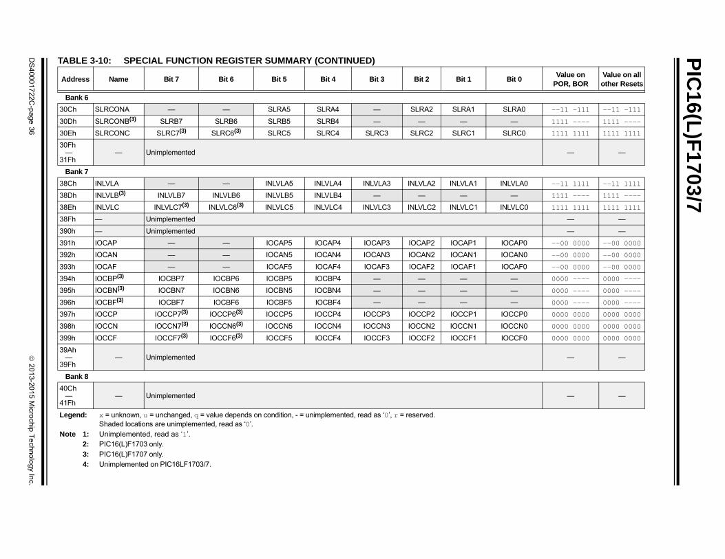
Bank 6
30Ch SLRCONA — — SLRA5 SLRA4 — SLRA2 SLRA1 SL
30Dh SLRCONB(3) SLRB7 SLRB6 SLRB5 SLRB4 — — —
30Eh SLRCONC SLRC7(3) SLRC6(3) SLRC5 SLRC4 SLRC3 SLRC2 SLRC1 SL
30Fh —31Fh
— Unimplemented
Bank 7
38Ch INLVLA — — INLVLA5 INLVLA4 INLVLA3 INLVLA2 INLVLA1 INL
38Dh INLVLB(3) INLVLB7 INLVLB6 INLVLB5 INLVLB4 — — —
38Eh INLVLC INLVLC7(3) INLVLC6(3) INLVLC5 INLVLC4 INLVLC3 INLVLC2 INLVLC1 INL
38Fh — Unimplemented
390h — Unimplemented
391h IOCAP — — IOCAP5 IOCAP4 IOCAP3 IOCAP2 IOCAP1 IOC
392h IOCAN — — IOCAN5 IOCAN4 IOCAN3 IOCAN2 IOCAN1 IOC
393h IOCAF — — IOCAF5 IOCAF4 IOCAF3 IOCAF2 IOCAF1 IOC
394h IOCBP(3) IOCBP7 IOCBP6 IOCBP5 IOCBP4 — — —
395h IOCBN(3) IOCBN7 IOCBN6 IOCBN5 IOCBN4 — — —
396h IOCBF(3) IOCBF7 IOCBF6 IOCBF5 IOCBF4 — — —
397h IOCCP IOCCP7(3) IOCCP6(3) IOCCP5 IOCCP4 IOCCP3 IOCCP2 IOCCP1 IOC
398h IOCCN IOCCN7(3) IOCCN6(3) IOCCN5 IOCCN4 IOCCN3 IOCCN2 IOCCN1 IOC
399h IOCCF IOCCF7(3) IOCCF6(3) IOCCF5 IOCCF4 IOCCF3 IOCCF2 IOCCF1 IOC
39Ah —39Fh
— Unimplemented
Bank 8
40Ch —41Fh
— Unimplemented
TABLE 3-10: SPECIAL FUNCTION REGISTER SUMMARY (CONTINUED)
Address Name Bit 7 Bit 6 Bit 5 Bit 4 Bit 3 Bit 2 Bit 1 B
Legend: x = unknown, u = unchanged, q = value depends on condition, - = unimplemented, read as ‘0’, r = reserved. Shaded locations are unimplemented, read as ‘0’.
Note 1: Unimplemented, read as ‘1’.2: PIC16(L)F1703 only.3: PIC16(L)F1707 only.4: Unimplemented on PIC16LF1703/7.
2
01
3-2
01
5 M
icroch
ip T
ech
no
log
y Inc.
DS
40
00
17
22
C-p
ag
e 3
7
PIC
16(L)F
1703/7
B
— —
B
50 —51
— —
51 > 00-0 --00 00-0 --00
51—51
— —
51 > 00-0 --00 00-0 --00
51 —51
— —
B
D— —
TA
A it 0Value on
POR, BORValue on all other Resets
Le
No
ank 9
48Ch to
49Fh— Unimplemented
ank 10
Ch
0h— Unimplemented
1h OPA1CON OPA1EN OPA1SP — OPA1UG — — OPA1PCH<1:0
2h
4h— Unimplemented
5h OPA2CON OPA2EN OPA2SP — OPA2UG — — OPA2PCH<1:0
6h
Fh— Unimplemented
ank 11-27
58Ch/ 59Fh
—8Ch/
D9Fh
— Unimplemented
BLE 3-10: SPECIAL FUNCTION REGISTER SUMMARY (CONTINUED)
ddress Name Bit 7 Bit 6 Bit 5 Bit 4 Bit 3 Bit 2 Bit 1 B
gend: x = unknown, u = unchanged, q = value depends on condition, - = unimplemented, read as ‘0’, r = reserved. Shaded locations are unimplemented, read as ‘0’.
te 1: Unimplemented, read as ‘1’.2: PIC16(L)F1703 only.3: PIC16(L)F1707 only.4: Unimplemented on PIC16LF1703/7.

PIC
16(L)F
1703/7
DS
40
00
17
22
C-p
ag
e 3
8
20
13
-20
15
Micro
chip
Te
chn
olo
gy In
c.
— —
OCKED ---- ---0 ---- ---0
---0 0010 ---u uuuu
---0 0010 ---u uuuu
---0 0101 ---u uuuu
---0 0100 ---u uuuu
---1 0101 ---u uuuu
---1 0011 ---u uuuu
— —
---1 0000(3) ---u uuuu
---0 1110(4) ---u uuuu
---1 0001(3) ---u uuuu
---0 1100(4) ---u uuuu
---1 0011(3) ---u uuuu
---1 0110(4) ---u uuuu
— —
it 0Value on
POR, BORValue on all other Resets
Bank 28
E0Ch —E0Eh
— Unimplemented
E0Fh PPSLOCK — — — — — — — PPSL
E10h INTPPS — — — INTPPS<4:0>
E11h T0CKIPPS — — — T0CKIPPS<4:0>
E12h T1CKIPPS — — — T1CKIPPS<4:0>
E13h T1GPPS — — — T1GPPS<4:0>
E14h CCP1PPS — — — CCP1PPS<4:0>
E15h CCP2PPS — — — CCP2PPS<4:0>
E16htoE1Fh
— Unimplemented
E20h SSPCLKPPS— — — SSPCLKPPS<4:0>
— — — SSPCLKPPS<4:0>
E21h SSPDATPPS— — — SSPDATPPS<4:0>
— — — SSPDATPPS<4:0>
E22h SSPSSPPS— — — SSPSSPPS<4:0>
— — — SSPSSPPS<4:0>
E23htoE6Fh
— Unimplemented
TABLE 3-10: SPECIAL FUNCTION REGISTER SUMMARY (CONTINUED)
Address Name Bit 7 Bit 6 Bit 5 Bit 4 Bit 3 Bit 2 Bit 1 B
Legend: x = unknown, u = unchanged, q = value depends on condition, - = unimplemented, read as ‘0’, r = reserved. Shaded locations are unimplemented, read as ‘0’.
Note 1: Unimplemented, read as ‘1’.2: PIC16(L)F1703 only.3: PIC16(L)F1707 only.4: Unimplemented on PIC16LF1703/7.
2
01
3-2
01
5 M
icroch
ip T
ech
no
log
y Inc.
DS
40
00
17
22
C-p
ag
e 3
9
PIC
16(L)F
1703/7
B
E8 —E8
— —
E9 ---0 0000 ---u uuuu
E9 ---0 0000 ---u uuuu
E9 ---0 0000 ---u uuuu
E9 — —
E9 ---0 0000 ---u uuuu
E9 ---0 0000 ---u uuuu
E9toE9
— —
EA ---0 0000 ---u uuuu
EA ---0 0000 ---u uuuu
EA ---0 0000 ---u uuuu
EA ---0 0000 ---u uuuu
EA ---0 0000 ---u uuuu
EA ---0 0000 ---u uuuu
EA —EE
— —
B
F0 —F6
— —
TA
A it 0Value on
POR, BORValue on all other Resets
Le
No
ank 29
Ch
Fh— Unimplemented
0h RA0PPS — — — RA0PPS<4:0>
1h RA1PPS — — — RA1PPS<4:0>
2h RA2PPS — — — RA2PPS<4:0>
3h — Unimplemented
4h RA4PPS — — — RA4PPS<4:0>
5h RA5PPS — — — RA5PPS<4:0>
6h
Fh— Unimplemented
0h RC0PPS — — — RC0PPS<4:0>
1h RC1PPS — — — RC1PPS<4:0>
2h RC2PPS — — — RC2PPS<4:0>
3h RC3PPS — — — RC3PPS<4:0>
4h RC4PPS — — — RC4PPS<4:0>
5h RC5PPS — — — RC5PPS<4:0>
6h
Fh— Unimplemented
ank 30
Ch
Fh— Unimplemented
BLE 3-10: SPECIAL FUNCTION REGISTER SUMMARY (CONTINUED)
ddress Name Bit 7 Bit 6 Bit 5 Bit 4 Bit 3 Bit 2 Bit 1 B
gend: x = unknown, u = unchanged, q = value depends on condition, - = unimplemented, read as ‘0’, r = reserved. Shaded locations are unimplemented, read as ‘0’.
te 1: Unimplemented, read as ‘1’.2: PIC16(L)F1703 only.3: PIC16(L)F1707 only.4: Unimplemented on PIC16LF1703/7.
PIC
16(L)F
1703/7
DS
40
00
17
22
C-p
ag
e 4
0
20
13
-20
15
Micro
chip
Te
chn
olo
gy In
c.
— —
C ---- -xxx ---- -xxx
xxxx xxxx uuuu uuuu
---x xxxx ---u uuuu
-xxx xxxx uuuu uuuu
xxxx xxxx uuuu uuuu
xxxx xxxx uuuu uuuu
xxxx xxxx uuuu uuuu
xxxx xxxx uuuu uuuu
— —
---x xxxx ---x xxxx
xxxx xxxx uuuu uuuu
-xxx xxxx -uuu uuuu
it 0Value on
POR, BORValue on all other Resets
Bank 31
F8Ehto
FE3h— Unimplemented
FE4h STATUS_
SHAD— — — — —
Z DC
FE5h WREG_SHAD
Working Register Shadow
FE6h BSR_
SHAD
— — — Bank Select Register Shadow
FE7h PCLATH_SHAD
— Program Counter Latch High Register Shadow
FE8h FSR0L_SHAD
Indirect Data Memory Address 0 Low Pointer Shadow
FE9h FSR0H_SHAD
Indirect Data Memory Address 0 High Pointer Shadow
FEAh FSR1L_SHAD
Indirect Data Memory Address 1 Low Pointer Shadow
FEBh FSR1H_SHAD
Indirect Data Memory Address 1 High Pointer Shadow
FECh — Unimplemented
FEDh STKPTR — — — Current Stack Pointer
FEEh TOSL Top of Stack Low byte
FEFh TOSH — Top of Stack High byte
TABLE 3-10: SPECIAL FUNCTION REGISTER SUMMARY (CONTINUED)
Address Name Bit 7 Bit 6 Bit 5 Bit 4 Bit 3 Bit 2 Bit 1 B
Legend: x = unknown, u = unchanged, q = value depends on condition, - = unimplemented, read as ‘0’, r = reserved. Shaded locations are unimplemented, read as ‘0’.
Note 1: Unimplemented, read as ‘1’.2: PIC16(L)F1703 only.3: PIC16(L)F1707 only.4: Unimplemented on PIC16LF1703/7.
PIC16(L)F1703/7
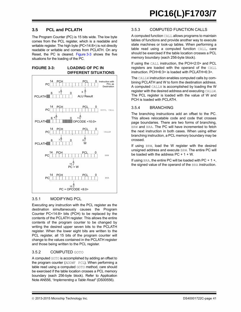
3.5 PCL and PCLATH
The Program Counter (PC) is 15 bits wide. The low bytecomes from the PCL register, which is a readable andwritable register. The high byte (PC<14:8>) is not directlyreadable or writable and comes from PCLATH. On anyReset, the PC is cleared. Figure 3-3 shows the fivesituations for the loading of the PC.
FIGURE 3-3: LOADING OF PC IN DIFFERENT SITUATIONS
3.5.1 MODIFYING PCL
Executing any instruction with the PCL register as thedestination simultaneously causes the ProgramCounter PC<14:8> bits (PCH) to be replaced by thecontents of the PCLATH register. This allows the entirecontents of the program counter to be changed bywriting the desired upper seven bits to the PCLATHregister. When the lower eight bits are written to thePCL register, all 15 bits of the program counter willchange to the values contained in the PCLATH registerand those being written to the PCL register.
3.5.2 COMPUTED GOTO
A computed GOTO is accomplished by adding an offset tothe program counter (ADDWF PCL). When performing atable read using a computed GOTO method, care shouldbe exercised if the table location crosses a PCL memoryboundary (each 256-byte block). Refer to ApplicationNote AN556, “Implementing a Table Read” (DS00556).
3.5.3 COMPUTED FUNCTION CALLS
A computed function CALL allows programs to maintaintables of functions and provide another way to executestate machines or look-up tables. When performing atable read using a computed function CALL, careshould be exercised if the table location crosses a PCLmemory boundary (each 256-byte block).
If using the CALL instruction, the PCH<2:0> and PCLregisters are loaded with the operand of the CALLinstruction. PCH<6:3> is loaded with PCLATH<6:3>.
The CALLW instruction enables computed calls by com-bining PCLATH and W to form the destination address.A computed CALLW is accomplished by loading the Wregister with the desired address and executing CALLW.The PCL register is loaded with the value of W andPCH is loaded with PCLATH.
3.5.4 BRANCHING
The branching instructions add an offset to the PC.This allows relocatable code and code that crossespage boundaries. There are two forms of branching,BRW and BRA. The PC will have incremented to fetchthe next instruction in both cases. When using eitherbranching instruction, a PCL memory boundary may becrossed.
If using BRW, load the W register with the desiredunsigned address and execute BRW. The entire PC willbe loaded with the address PC + 1 + W.
If using BRA, the entire PC will be loaded with PC + 1 +,the signed value of the operand of the BRA instruction.
PCLPCH 014PC
06 7
ALU Result
8
PCLATH
PCLPCH 014PC
06 4
OPCODE <10:0>11
PCLATH
PCLPCH 014PC
06 7
W8
PCLATH
Instruction with PCL as
Destination
GOTO, CALL
CALLW
PCLPCH 014PC
PC + W15
BRW
PCLPCH 014PC
PC + OPCODE <8:0>15
BRA
2013-2015 Microchip Technology Inc. DS40001722C-page 41
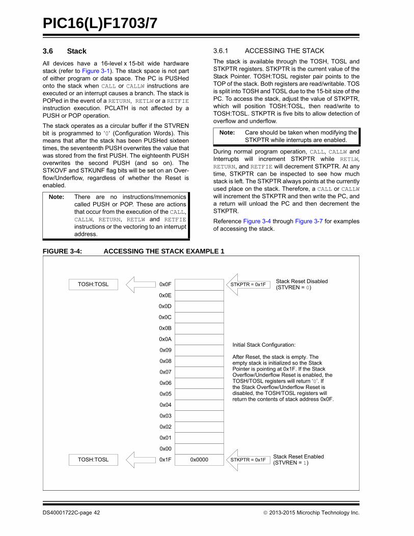
PIC16(L)F1703/7
3.6 Stack
All devices have a 16-level x 15-bit wide hardwarestack (refer to Figure 3-1). The stack space is not partof either program or data space. The PC is PUSHedonto the stack when CALL or CALLW instructions areexecuted or an interrupt causes a branch. The stack isPOPed in the event of a RETURN, RETLW or a RETFIEinstruction execution. PCLATH is not affected by aPUSH or POP operation.
The stack operates as a circular buffer if the STVRENbit is programmed to ‘0‘ (Configuration Words). Thismeans that after the stack has been PUSHed sixteentimes, the seventeenth PUSH overwrites the value thatwas stored from the first PUSH. The eighteenth PUSHoverwrites the second PUSH (and so on). TheSTKOVF and STKUNF flag bits will be set on an Over-flow/Underflow, regardless of whether the Reset isenabled.
3.6.1 ACCESSING THE STACK
The stack is available through the TOSH, TOSL andSTKPTR registers. STKPTR is the current value of theStack Pointer. TOSH:TOSL register pair points to theTOP of the stack. Both registers are read/writable. TOSis split into TOSH and TOSL due to the 15-bit size of thePC. To access the stack, adjust the value of STKPTR,which will position TOSH:TOSL, then read/write toTOSH:TOSL. STKPTR is five bits to allow detection ofoverflow and underflow.
During normal program operation, CALL, CALLW andInterrupts will increment STKPTR while RETLW,RETURN, and RETFIE will decrement STKPTR. At anytime, STKPTR can be inspected to see how muchstack is left. The STKPTR always points at the currentlyused place on the stack. Therefore, a CALL or CALLWwill increment the STKPTR and then write the PC, anda return will unload the PC and then decrement theSTKPTR.
Reference Figure 3-4 through Figure 3-7 for examplesof accessing the stack.
FIGURE 3-4: ACCESSING THE STACK EXAMPLE 1
Note: There are no instructions/mnemonicscalled PUSH or POP. These are actionsthat occur from the execution of the CALL,CALLW, RETURN, RETLW and RETFIEinstructions or the vectoring to an interruptaddress.
Note: Care should be taken when modifying theSTKPTR while interrupts are enabled.
0x0F
0x0E
0x0D
0x0C
0x0B
0x0A
0x09
0x08
0x07
0x06
0x05
0x04
0x03
0x02
0x01
0x00
0x0000
STKPTR = 0x1F
Initial Stack Configuration:
After Reset, the stack is empty. Theempty stack is initialized so the StackPointer is pointing at 0x1F. If the StackOverflow/Underflow Reset is enabled, theTOSH/TOSL registers will return ‘0’. Ifthe Stack Overflow/Underflow Reset isdisabled, the TOSH/TOSL registers willreturn the contents of stack address 0x0F.
0x1F STKPTR = 0x1F
Stack Reset Disabled(STVREN = 0)
Stack Reset Enabled(STVREN = 1)
TOSH:TOSL
TOSH:TOSL
DS40001722C-page 42 2013-2015 Microchip Technology Inc.
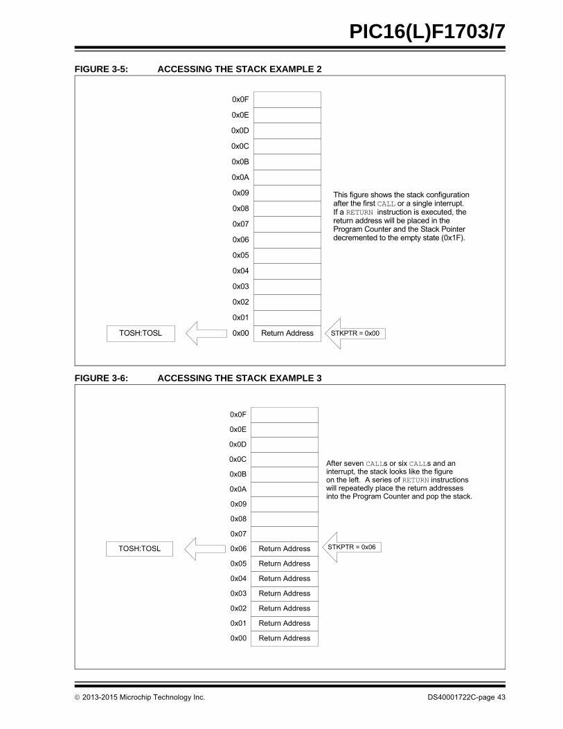
PIC16(L)F1703/7
FIGURE 3-5: ACCESSING THE STACK EXAMPLE 2
FIGURE 3-6: ACCESSING THE STACK EXAMPLE 3
0x0F
0x0E
0x0D
0x0C
0x0B
0x0A
0x09
0x08
0x07
0x06
0x05
0x04
0x03
0x02
0x01
Return Address0x00 STKPTR = 0x00
This figure shows the stack configurationafter the first CALL or a single interrupt.If a RETURN instruction is executed, thereturn address will be placed in theProgram Counter and the Stack Pointerdecremented to the empty state (0x1F).
TOSH:TOSL
0x0F
0x0E
0x0D
0x0C
0x0B
0x0A
0x09
0x08
0x07
Return Address0x06
Return Address0x05
Return Address0x04
Return Address0x03
Return Address0x02
Return Address0x01
Return Address0x00
STKPTR = 0x06
After seven CALLs or six CALLs and aninterrupt, the stack looks like the figureon the left. A series of RETURN instructionswill repeatedly place the return addresses into the Program Counter and pop the stack.
TOSH:TOSL
2013-2015 Microchip Technology Inc. DS40001722C-page 43
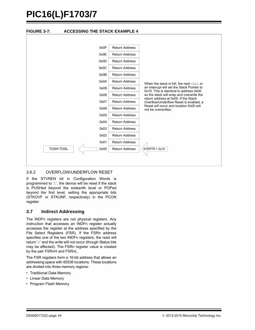
PIC16(L)F1703/7
FIGURE 3-7: ACCESSING THE STACK EXAMPLE 4
3.6.2 OVERFLOW/UNDERFLOW RESET
If the STVREN bit in Configuration Words isprogrammed to ‘1’, the device will be reset if the stackis PUSHed beyond the sixteenth level or POPedbeyond the first level, setting the appropriate bits(STKOVF or STKUNF, respectively) in the PCONregister.
3.7 Indirect Addressing
The INDFn registers are not physical registers. Anyinstruction that accesses an INDFn register actuallyaccesses the register at the address specified by theFile Select Registers (FSR). If the FSRn addressspecifies one of the two INDFn registers, the read willreturn ‘0’ and the write will not occur (though Status bitsmay be affected). The FSRn register value is createdby the pair FSRnH and FSRnL.
The FSR registers form a 16-bit address that allows anaddressing space with 65536 locations. These locationsare divided into three memory regions:
• Traditional Data Memory
• Linear Data Memory
• Program Flash Memory
0x0F
0x0E
0x0D
0x0C
0x0B
0x0A
0x09
0x08
0x07
0x06
0x05
0x04
0x03
0x02
0x01
Return Address0x00 STKPTR = 0x10
When the stack is full, the next CALL oran interrupt will set the Stack Pointer to0x10. This is identical to address 0x00so the stack will wrap and overwrite thereturn address at 0x00. If the StackOverflow/Underflow Reset is enabled, aReset will occur and location 0x00 willnot be overwritten.
Return Address
Return Address
Return Address
Return Address
Return Address
Return Address
Return Address
Return Address
Return Address
Return Address
Return Address
Return Address
Return Address
Return Address
Return Address
TOSH:TOSL
DS40001722C-page 44 2013-2015 Microchip Technology Inc.
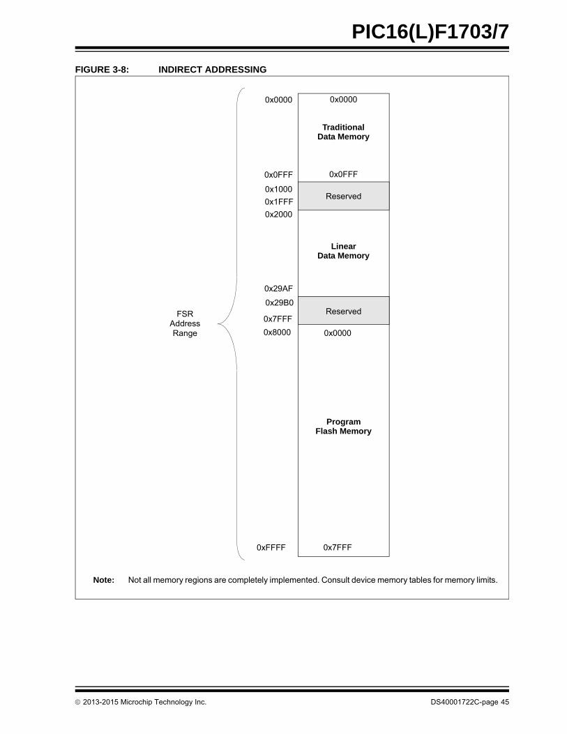
PIC16(L)F1703/7
FIGURE 3-8: INDIRECT ADDRESSING
0x0000
0x0FFF
Traditional
FSRAddressRange
Data Memory
0x1000Reserved
LinearData Memory
Reserved
0x2000
0x29AF
0x29B0
0x7FFF
0x8000
0xFFFF
0x0000
0x0FFF
0x0000
0x7FFF
ProgramFlash Memory
Note: Not all memory regions are completely implemented. Consult device memory tables for memory limits.
0x1FFF
2013-2015 Microchip Technology Inc. DS40001722C-page 45
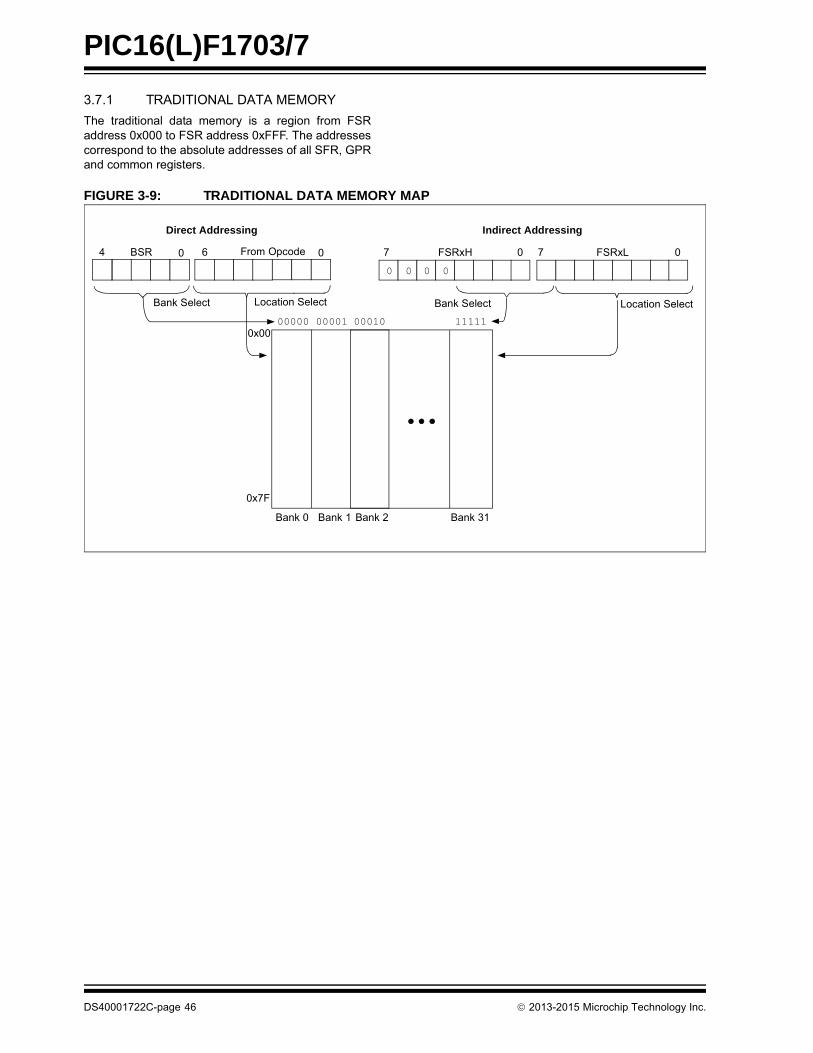
PIC16(L)F1703/7
3.7.1 TRADITIONAL DATA MEMORY
The traditional data memory is a region from FSRaddress 0x000 to FSR address 0xFFF. The addressescorrespond to the absolute addresses of all SFR, GPRand common registers.
FIGURE 3-9: TRADITIONAL DATA MEMORY MAP
Indirect AddressingDirect Addressing
Bank Select Location Select
4 BSR 6 0From Opcode FSRxL7 0
Bank Select Location Select
00000 00001 00010 111110x00
0x7F
Bank 0 Bank 1 Bank 2 Bank 31
0 FSRxH7 0
0 0 0 0
DS40001722C-page 46 2013-2015 Microchip Technology Inc.

PIC16(L)F1703/7
3.7.2 LINEAR DATA MEMORY
The linear data memory is the region from FSRaddress 0x2000 to FSR address 0x29AF. This region isa virtual region that points back to the 80-byte blocks ofGPR memory in all the banks.
Unimplemented memory reads as 0x00. Use of thelinear data memory region allows buffers to be largerthan 80 bytes because incrementing the FSR beyondone bank will go directly to the GPR memory of the nextbank.
The 16 bytes of common memory are not included inthe linear data memory region.
FIGURE 3-10: LINEAR DATA MEMORY MAP
3.7.3 PROGRAM FLASH MEMORY
To make constant data access easier, the entireprogram Flash memory is mapped to the upper half ofthe FSR address space. When the MSB of FSRnH isset, the lower 15 bits are the address in programmemory which will be accessed through INDF. Only thelower eight bits of each memory location is accessiblevia INDF. Writing to the program Flash memory cannotbe accomplished via the FSR/INDF interface. Allinstructions that access program Flash memory via theFSR/INDF interface will require one additionalinstruction cycle to complete.
FIGURE 3-11: PROGRAM FLASH MEMORY MAP
7
0 170 0
Location Select 0x2000
FSRnH FSRnL
0x020
Bank 0
0x06F0x0A0
Bank 1
0x0EF
0x120
Bank 2
0x16F
0xF20
Bank 30
0xF6F0x29AF
0
7
170 0
Location Select 0x8000
FSRnH FSRnL
0x0000
0x7FFF0xFFFF
ProgramFlashMemory(low 8bits)
2013-2015 Microchip Technology Inc. DS40001722C-page 47
PIC16(L)F1703/7
4.0 DEVICE CONFIGURATION
Device configuration consists of Configuration Words,Code Protection and Device ID.
4.1 Configuration Words
There are several Configuration Word bits that allowdifferent oscillator and memory protection options.These are implemented as Configuration Word 1 at8007h and Configuration Word 2 at 8008h.
Note: The DEBUG bit in Configuration Words ismanaged automatically by devicedevelopment tools including debuggersand programmers. For normal deviceoperation, this bit should be maintained asa ‘1’.
DS40001722C-page 48 2013-2015 Microchip Technology Inc.
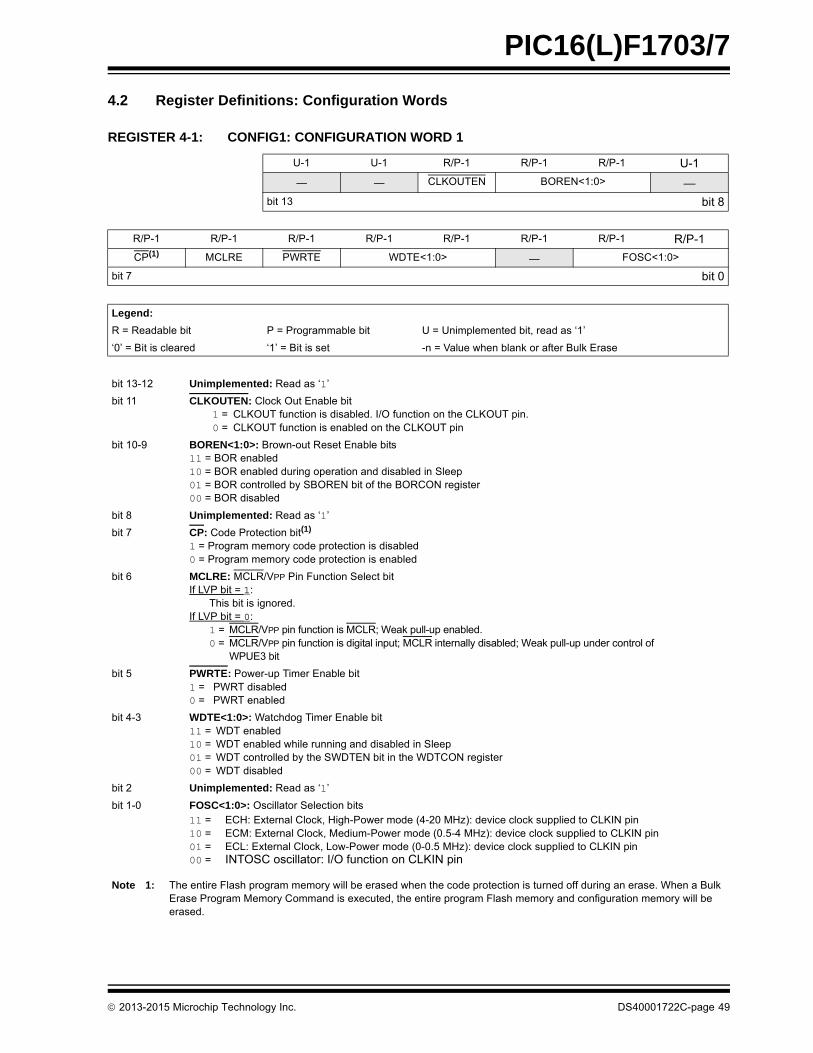
PIC16(L)F1703/7
4.2 Register Definitions: Configuration Words
REGISTER 4-1: CONFIG1: CONFIGURATION WORD 1
U-1 U-1 R/P-1 R/P-1 R/P-1 U-1
— — CLKOUTEN BOREN<1:0> —
bit 13 bit 8
R/P-1 R/P-1 R/P-1 R/P-1 R/P-1 R/P-1 R/P-1 R/P-1
CP(1) MCLRE PWRTE WDTE<1:0> — FOSC<1:0>
bit 7 bit 0
Legend:
R = Readable bit P = Programmable bit U = Unimplemented bit, read as ‘1’
‘0’ = Bit is cleared ‘1’ = Bit is set -n = Value when blank or after Bulk Erase
bit 13-12 Unimplemented: Read as ‘1’
bit 11 CLKOUTEN: Clock Out Enable bit1 = CLKOUT function is disabled. I/O function on the CLKOUT pin.0 = CLKOUT function is enabled on the CLKOUT pin
bit 10-9 BOREN<1:0>: Brown-out Reset Enable bits11 = BOR enabled10 = BOR enabled during operation and disabled in Sleep01 = BOR controlled by SBOREN bit of the BORCON register00 = BOR disabled
bit 8 Unimplemented: Read as ‘1’
bit 7 CP: Code Protection bit(1)
1 = Program memory code protection is disabled0 = Program memory code protection is enabled
bit 6 MCLRE: MCLR/VPP Pin Function Select bitIf LVP bit = 1:
This bit is ignored.If LVP bit = 0:
1 = MCLR/VPP pin function is MCLR; Weak pull-up enabled.0 = MCLR/VPP pin function is digital input; MCLR internally disabled; Weak pull-up under control of
WPUE3 bit
bit 5 PWRTE: Power-up Timer Enable bit1 = PWRT disabled0 = PWRT enabled
bit 4-3 WDTE<1:0>: Watchdog Timer Enable bit11 = WDT enabled10 = WDT enabled while running and disabled in Sleep01 = WDT controlled by the SWDTEN bit in the WDTCON register00 = WDT disabled
bit 2 Unimplemented: Read as ‘1’
bit 1-0 FOSC<1:0>: Oscillator Selection bits11 = ECH: External Clock, High-Power mode (4-20 MHz): device clock supplied to CLKIN pin10 = ECM: External Clock, Medium-Power mode (0.5-4 MHz): device clock supplied to CLKIN pin01 = ECL: External Clock, Low-Power mode (0-0.5 MHz): device clock supplied to CLKIN pin00 = INTOSC oscillator: I/O function on CLKIN pin
Note 1: The entire Flash program memory will be erased when the code protection is turned off during an erase. When a Bulk Erase Program Memory Command is executed, the entire program Flash memory and configuration memory will be erased.
2013-2015 Microchip Technology Inc. DS40001722C-page 49
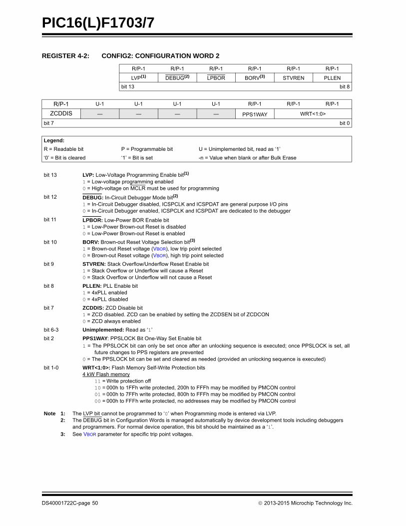
PIC16(L)F1703/7
REGISTER 4-2: CONFIG2: CONFIGURATION WORD 2
R/P-1 R/P-1 R/P-1 R/P-1 R/P-1 R/P-1
LVP(1) DEBUG(2) LPBOR BORV(3) STVREN PLLEN
bit 13 bit 8
R/P-1 U-1 U-1 U-1 U-1 R/P-1 R/P-1 R/P-1
ZCDDIS — — — — PPS1WAY WRT<1:0>
bit 7 bit 0
Legend:
R = Readable bit P = Programmable bit U = Unimplemented bit, read as ‘1’
‘0’ = Bit is cleared ‘1’ = Bit is set -n = Value when blank or after Bulk Erase
bit 13 LVP: Low-Voltage Programming Enable bit(1)
1 = Low-voltage programming enabled0 = High-voltage on MCLR must be used for programming
bit 12 DEBUG: In-Circuit Debugger Mode bit(2)
1 = In-Circuit Debugger disabled, ICSPCLK and ICSPDAT are general purpose I/O pins0 = In-Circuit Debugger enabled, ICSPCLK and ICSPDAT are dedicated to the debugger
bit 11 LPBOR: Low-Power BOR Enable bit1 = Low-Power Brown-out Reset is disabled0 = Low-Power Brown-out Reset is enabled
bit 10 BORV: Brown-out Reset Voltage Selection bit(3)
1 = Brown-out Reset voltage (VBOR), low trip point selected0 = Brown-out Reset voltage (VBOR), high trip point selected
bit 9 STVREN: Stack Overflow/Underflow Reset Enable bit1 = Stack Overflow or Underflow will cause a Reset0 = Stack Overflow or Underflow will not cause a Reset
bit 8 PLLEN: PLL Enable bit1 = 4xPLL enabled0 = 4xPLL disabled
bit 7 ZCDDIS: ZCD Disable bit1 = ZCD disabled. ZCD can be enabled by setting the ZCDSEN bit of ZCDCON0 = ZCD always enabled
bit 6-3 Unimplemented: Read as ‘1’
bit 2 PPS1WAY: PPSLOCK Bit One-Way Set Enable bit1 = The PPSLOCK bit can only be set once after an unlocking sequence is executed; once PPSLOCK is set, all
future changes to PPS registers are prevented0 = The PPSLOCK bit can be set and cleared as needed (provided an unlocking sequence is executed)
bit 1-0 WRT<1:0>: Flash Memory Self-Write Protection bits4 kW Flash memory
11 = Write protection off10 = 000h to 1FFh write protected, 200h to FFFh may be modified by PMCON control01 = 000h to 7FFh write protected, 800h to FFFh may be modified by PMCON control00 = 000h to FFFh write protected, no addresses may be modified by PMCON control
Note 1: The LVP bit cannot be programmed to ‘0’ when Programming mode is entered via LVP.2: The DEBUG bit in Configuration Words is managed automatically by device development tools including debuggers
and programmers. For normal device operation, this bit should be maintained as a ‘1’.3: See VBOR parameter for specific trip point voltages.
DS40001722C-page 50 2013-2015 Microchip Technology Inc.
PIC16(L)F1703/7
4.3 Code Protection
Code protection allows the device to be protected fromunauthorized access. Program memory protection iscontrolled independently. Internal access to theprogram memory is unaffected by any code protectionsetting.
4.3.1 PROGRAM MEMORY PROTECTION
The entire program memory space is protected fromexternal reads and writes by the CP bit in ConfigurationWords. When CP = 0, external reads and writes ofprogram memory are inhibited and a read will return all‘0’s. The CPU can continue to read program memory,regardless of the protection bit settings. Writing theprogram memory is dependent upon the writeprotection setting. See Section 4.4 “WriteProtection” for more information.
4.4 Write Protection
Write protection allows the device to be protected fromunintended self-writes. Applications, such as bootloader software, can be protected while allowing otherregions of the program memory to be modified.
The WRT<1:0> bits in Configuration Words define thesize of the program memory block that is protected.
4.5 User ID
Four memory locations (8000h-8003h) are designatedas ID locations where the user can store checksum orother code identification numbers. These locations arereadable and writable during normal execution. SeeSection 10.4 “User ID, Device ID and ConfigurationWord Access” for more information on accessingthese memory locations. For more information onchecksum calculation, see the “PIC16(L)F170XMemory Programming Specification” (DS41683).
2013-2015 Microchip Technology Inc. DS40001722C-page 51

PIC16(L)F1703/7
4.6 Device ID and Revision ID
The 14-bit device ID word is located at 8006h and the14-bit revision ID is located at 8005h. These locationsare read-only and cannot be erased or modified. SeeSection 10.4 “User ID, Device ID and ConfigurationWord Access” for more information on accessingthese memory locations.
Development tools, such as device programmers anddebuggers, may be used to read the Device ID andRevision ID.
4.7 Register Definitions: Device and Revision
REGISTER 4-3: DEVID: DEVICE ID REGISTER
R R R R R R
DEV<13:8>
bit 13 bit 8
R R R R R R R R
DEV<7:0>
bit 7 bit 0
Legend:
R = Readable bit
‘1’ = Bit is set ‘0’ = Bit is cleared
bit 13-0 DEV<13:0>: Device ID bits
REGISTER 4-4: REVID: REVISION ID REGISTER
R R R R R R
REV<13:8>
bit 13 bit 8
R R R R R R R R
REV<7:0>
bit 7 bit 0
Legend:
R = Readable bit
‘1’ = Bit is set ‘0’ = Bit is cleared
bit 13-0 REV<13:0>: Revision ID bits
Device DEVID<13:0> Values
PIC16F1703 11 0000 0100 0011 (3043h)
PIC16LF1703 11 0000 0100 0101 (3045h)
PIC16F1707 11 0000 0100 0010 (3042h)
PIC16LF1707 11 0000 0100 0100 (3044h)
DS40001722C-page 52 2013-2015 Microchip Technology Inc.

PIC16(L)F1703/7
5.0 RESETS
There are multiple ways to reset this device:
• Power-On Reset (POR)
• Brown-Out Reset (BOR)
• Low-Power Brown-Out Reset (LPBOR)
• MCLR Reset
• WDT Reset
• RESET instruction
• Stack Overflow
• Stack Underflow
• Programming mode exit
To allow VDD to stabilize, an optional Power-up Timercan be enabled to extend the Reset time after a BORor POR event.
A simplified block diagram of the On-Chip Reset Circuitis shown in Figure 5-1.
FIGURE 5-1: SIMPLIFIED BLOCK DIAGRAM OF ON-CHIP RESET CIRCUIT
DeviceReset
Power-on Reset
WDT Time-out
Brown-out Reset
LPBOR Reset
RESET Instruction
MCLRE
Sleep
BOR Active(1)
PWRTELFINTOSC
VDD
ICSP™ Programming Mode Exit
Stack UnderflowStack Overlfow
VPP/MCLR
R Power-up Timer
Rev. 10-000006A8/14/2013
Note 1: See Table 5-1 for BOR active conditions.
2013-2015 Microchip Technology Inc. DS40001722C-page 53
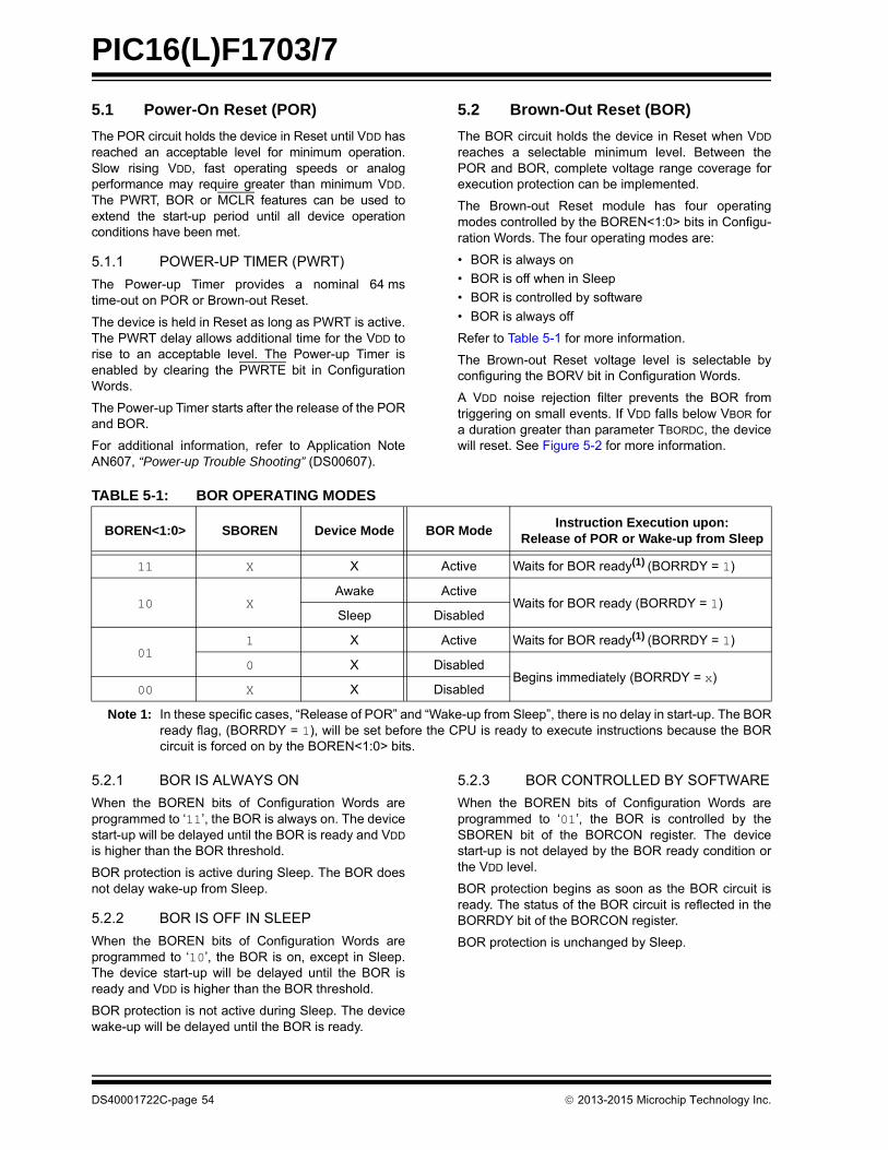
PIC16(L)F1703/7
5.1 Power-On Reset (POR)
The POR circuit holds the device in Reset until VDD hasreached an acceptable level for minimum operation.Slow rising VDD, fast operating speeds or analogperformance may require greater than minimum VDD.The PWRT, BOR or MCLR features can be used toextend the start-up period until all device operationconditions have been met.
5.1.1 POWER-UP TIMER (PWRT)
The Power-up Timer provides a nominal 64 mstime-out on POR or Brown-out Reset.
The device is held in Reset as long as PWRT is active.The PWRT delay allows additional time for the VDD torise to an acceptable level. The Power-up Timer isenabled by clearing the PWRTE bit in ConfigurationWords.
The Power-up Timer starts after the release of the PORand BOR.
For additional information, refer to Application NoteAN607, “Power-up Trouble Shooting” (DS00607).
5.2 Brown-Out Reset (BOR)
The BOR circuit holds the device in Reset when VDD
reaches a selectable minimum level. Between thePOR and BOR, complete voltage range coverage forexecution protection can be implemented.
The Brown-out Reset module has four operatingmodes controlled by the BOREN<1:0> bits in Configu-ration Words. The four operating modes are:
• BOR is always on
• BOR is off when in Sleep
• BOR is controlled by software
• BOR is always off
Refer to Table 5-1 for more information.
The Brown-out Reset voltage level is selectable byconfiguring the BORV bit in Configuration Words.
A VDD noise rejection filter prevents the BOR fromtriggering on small events. If VDD falls below VBOR fora duration greater than parameter TBORDC, the devicewill reset. See Figure 5-2 for more information.
TABLE 5-1: BOR OPERATING MODES
5.2.1 BOR IS ALWAYS ON
When the BOREN bits of Configuration Words areprogrammed to ‘11’, the BOR is always on. The devicestart-up will be delayed until the BOR is ready and VDD
is higher than the BOR threshold.
BOR protection is active during Sleep. The BOR doesnot delay wake-up from Sleep.
5.2.2 BOR IS OFF IN SLEEP
When the BOREN bits of Configuration Words areprogrammed to ‘10’, the BOR is on, except in Sleep.The device start-up will be delayed until the BOR isready and VDD is higher than the BOR threshold.
BOR protection is not active during Sleep. The devicewake-up will be delayed until the BOR is ready.
5.2.3 BOR CONTROLLED BY SOFTWARE
When the BOREN bits of Configuration Words areprogrammed to ‘01’, the BOR is controlled by theSBOREN bit of the BORCON register. The devicestart-up is not delayed by the BOR ready condition orthe VDD level.
BOR protection begins as soon as the BOR circuit isready. The status of the BOR circuit is reflected in theBORRDY bit of the BORCON register.
BOR protection is unchanged by Sleep.
BOREN<1:0> SBOREN Device Mode BOR ModeInstruction Execution upon:
Release of POR or Wake-up from Sleep
11 X X Active Waits for BOR ready(1) (BORRDY = 1)
10 XAwake Active
Waits for BOR ready (BORRDY = 1)Sleep Disabled
011 X Active Waits for BOR ready(1) (BORRDY = 1)
0 X DisabledBegins immediately (BORRDY = x)
00 X X Disabled
Note 1: In these specific cases, “Release of POR” and “Wake-up from Sleep”, there is no delay in start-up. The BORready flag, (BORRDY = 1), will be set before the CPU is ready to execute instructions because the BORcircuit is forced on by the BOREN<1:0> bits.
DS40001722C-page 54 2013-2015 Microchip Technology Inc.
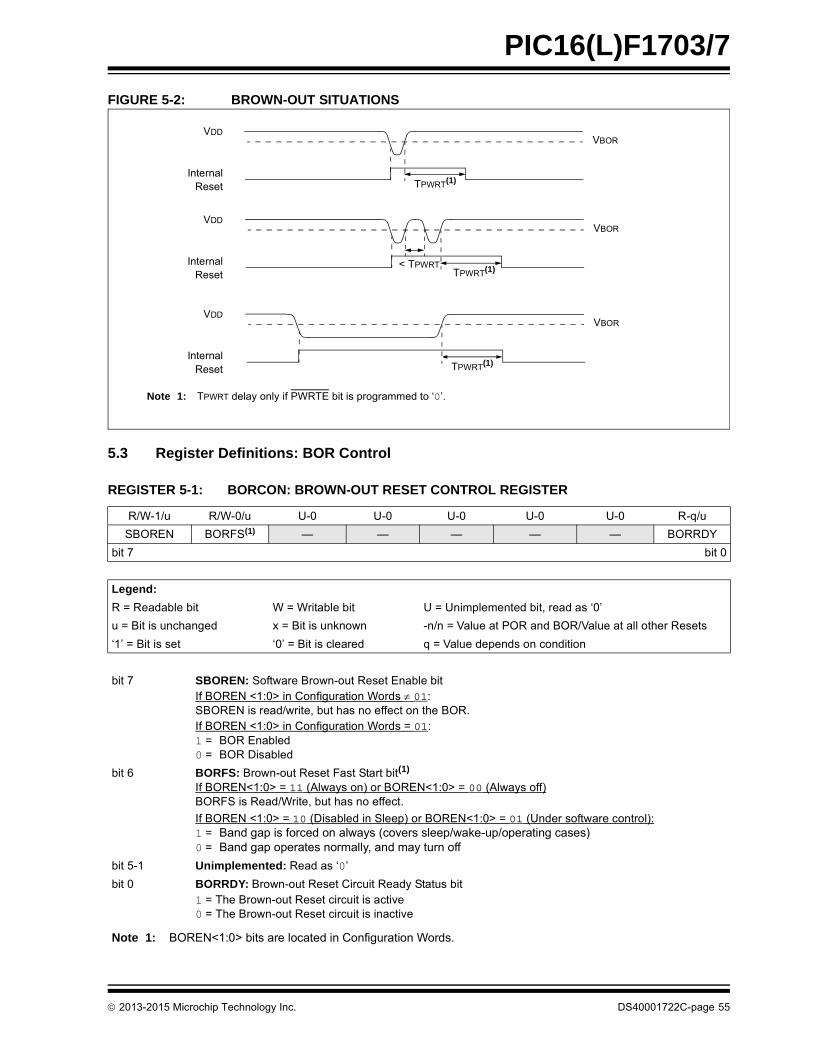
PIC16(L)F1703/7
FIGURE 5-2: BROWN-OUT SITUATIONS
5.3 Register Definitions: BOR Control
REGISTER 5-1: BORCON: BROWN-OUT RESET CONTROL REGISTER
R/W-1/u R/W-0/u U-0 U-0 U-0 U-0 U-0 R-q/u
SBOREN BORFS(1) — — — — — BORRDY
bit 7 bit 0
Legend:
R = Readable bit W = Writable bit U = Unimplemented bit, read as ‘0’
u = Bit is unchanged x = Bit is unknown -n/n = Value at POR and BOR/Value at all other Resets
‘1’ = Bit is set ‘0’ = Bit is cleared q = Value depends on condition
bit 7 SBOREN: Software Brown-out Reset Enable bitIf BOREN <1:0> in Configuration Words 01:SBOREN is read/write, but has no effect on the BOR.If BOREN <1:0> in Configuration Words = 01:1 = BOR Enabled0 = BOR Disabled
bit 6 BORFS: Brown-out Reset Fast Start bit(1)
If BOREN<1:0> = 11 (Always on) or BOREN<1:0> = 00 (Always off)BORFS is Read/Write, but has no effect.
If BOREN <1:0> = 10 (Disabled in Sleep) or BOREN<1:0> = 01 (Under software control):1 = Band gap is forced on always (covers sleep/wake-up/operating cases)0 = Band gap operates normally, and may turn off
bit 5-1 Unimplemented: Read as ‘0’
bit 0 BORRDY: Brown-out Reset Circuit Ready Status bit1 = The Brown-out Reset circuit is active0 = The Brown-out Reset circuit is inactive
Note 1: BOREN<1:0> bits are located in Configuration Words.
TPWRT(1)
VBOR VDD
InternalReset
VBOR VDD
InternalReset TPWRT(1)< TPWRT
TPWRT(1)
VBOR VDD
InternalReset
Note 1: TPWRT delay only if PWRTE bit is programmed to ‘0’.
2013-2015 Microchip Technology Inc. DS40001722C-page 55
PIC16(L)F1703/7
5.4 Low-Power Brown-Out Reset (LPBOR)
The Low-Power Brown-Out Reset (LPBOR) is anessential part of the Reset subsystem. Refer toFigure 5-1 to see how the BOR interacts with othermodules.
The LPBOR is used to monitor the external VDD pin.When too low of a voltage is detected, the device isheld in Reset. When this occurs, a register bit (BOR) ischanged to indicate that a BOR Reset has occurred.The same bit is set for both the BOR and the LPBOR.Refer to Register 5-2.
5.4.1 ENABLING LPBOR
The LPBOR is controlled by the LPBOR bit ofConfiguration Words. When the device is erased, theLPBOR module defaults to disabled.
5.4.1.1 LPBOR Module Output
The output of the LPBOR module is a signal indicatingwhether or not a Reset is to be asserted. This signal isOR’d together with the Reset signal of the BORmodule to provide the generic BOR signal, which goesto the PCON register and to the power control block.
5.5 MCLR
The MCLR is an optional external input that can resetthe device. The MCLR function is controlled by theMCLRE bit of Configuration Words and the LVP bit ofConfiguration Words (Table 5-2).
5.5.1 MCLR ENABLED
When MCLR is enabled and the pin is held low, thedevice is held in Reset. The MCLR pin is connected toVDD through an internal weak pull-up.
The device has a noise filter in the MCLR Reset path.The filter will detect and ignore small pulses.
5.5.2 MCLR DISABLED
When MCLR is disabled, the pin functions as a generalpurpose input and the internal weak pull-up is undersoftware control. See Section 11.1 “PORTA Regis-ters” for more information.
5.6 Watchdog Timer (WDT) Reset
The Watchdog Timer generates a Reset if the firmwaredoes not issue a CLRWDT instruction within the time-outperiod. The TO and PD bits in the STATUS register arechanged to indicate the WDT Reset. See Section 9.0“Watchdog Timer (WDT)” for more information.
5.7 RESET Instruction
A RESET instruction will cause a device Reset. The RIbit in the PCON register will be set to ‘0’. See Table 5-4for default conditions after a RESET instruction hasoccurred.
5.8 Stack Overflow/Underflow Reset
The device can reset when the Stack Overflows orUnderflows. The STKOVF or STKUNF bits of the PCONregister indicate the Reset condition. These Resets areenabled by setting the STVREN bit in ConfigurationWords. See Section 3.6.2 “Overflow/UnderflowReset” for more information.
5.9 Programming Mode Exit
Upon exit of Programming mode, the device willbehave as if a POR had just occurred.
5.10 Power-Up Timer
The Power-up Timer optionally delays device executionafter a BOR or POR event. This timer is typically used toallow VDD to stabilize before allowing the device to startrunning.
The Power-up Timer is controlled by the PWRTE bit ofConfiguration Words.
5.11 Start-up Sequence
Upon the release of a POR or BOR, the following mustoccur before the device will begin executing:
1. Power-up Timer runs to completion (if enabled).
2. Oscillator start-up timer runs to completion (ifrequired for oscillator source).
3. MCLR must be released (if enabled).
The total time-out will vary based on oscillator configu-ration and Power-up Timer configuration. SeeSection 6.0 “Oscillator Module (with Fail-SafeClock Monitor)” for more information.
The Power-up Timer and oscillator start-up timer runindependently of MCLR Reset. If MCLR is kept lowlong enough, the Power-up Timer and oscillatorstart-up timer will expire. Upon bringing MCLR high, thedevice will begin execution after 10 FOSC cycles (seeFigure 5-3). This is useful for testing purposes or tosynchronize more than one device operating in parallel.
TABLE 5-2: MCLR CONFIGURATION
MCLRE LVP MCLR
0 0 Disabled
1 0 Enabled
x 1 Enabled
Note: A Reset does not drive the MCLR pin low.
DS40001722C-page 56 2013-2015 Microchip Technology Inc.
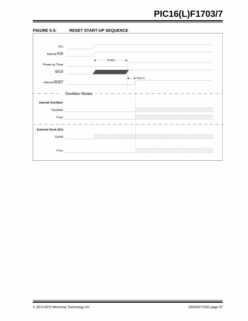
PIC16(L)F1703/7
FIGURE 5-3: RESET START-UP SEQUENCE
TMCLR
TPWRT
VDD
Internal POR
Power-up Timer
MCLR
Internal RESET
Oscillator Modes
Internal Oscillator
Oscillator
FOSC
External Clock (EC)
CLKIN
FOSC
2013-2015 Microchip Technology Inc. DS40001722C-page 57
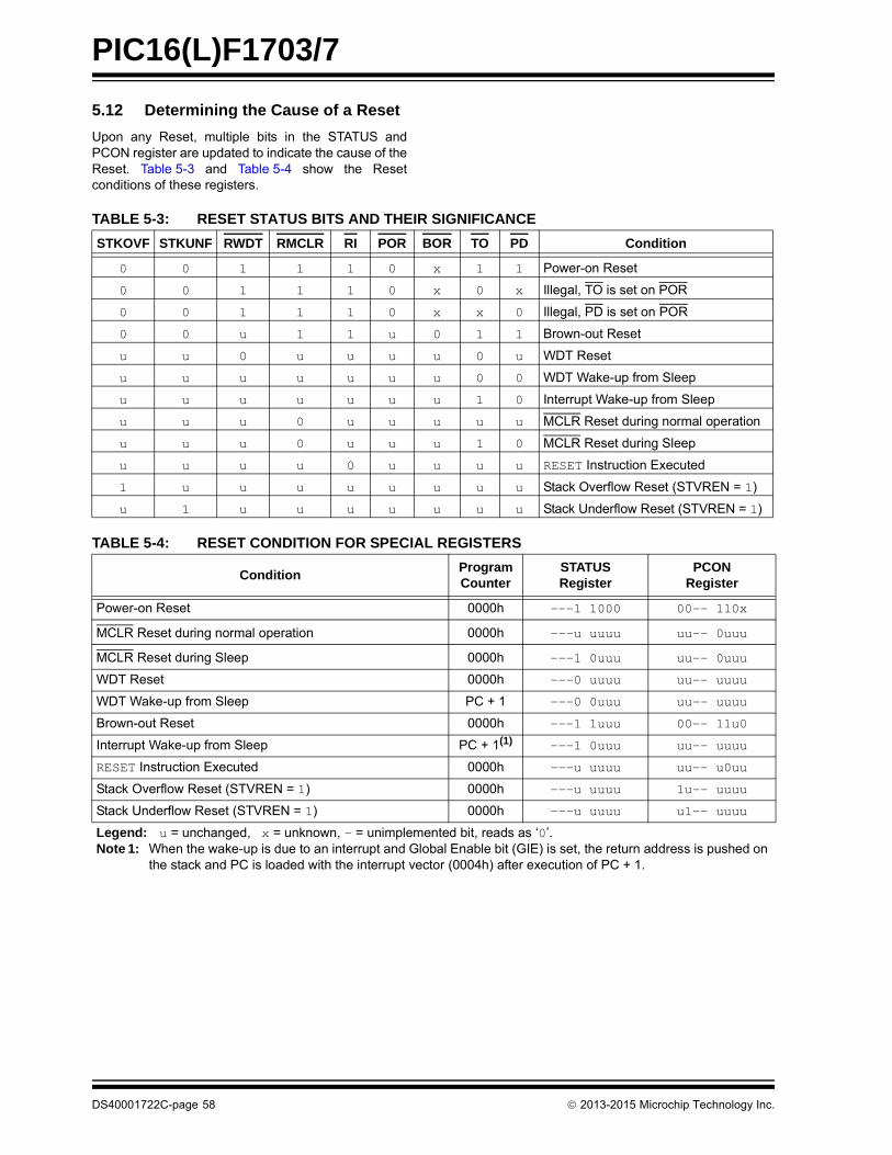
PIC16(L)F1703/7
5.12 Determining the Cause of a Reset
Upon any Reset, multiple bits in the STATUS andPCON register are updated to indicate the cause of theReset. Table 5-3 and Table 5-4 show the Resetconditions of these registers.
TABLE 5-3: RESET STATUS BITS AND THEIR SIGNIFICANCE
TABLE 5-4: RESET CONDITION FOR SPECIAL REGISTERS
STKOVF STKUNF RWDT RMCLR RI POR BOR TO PD Condition
0 0 1 1 1 0 x 1 1 Power-on Reset
0 0 1 1 1 0 x 0 x Illegal, TO is set on POR
0 0 1 1 1 0 x x 0 Illegal, PD is set on POR
0 0 u 1 1 u 0 1 1 Brown-out Reset
u u 0 u u u u 0 u WDT Reset
u u u u u u u 0 0 WDT Wake-up from Sleep
u u u u u u u 1 0 Interrupt Wake-up from Sleep
u u u 0 u u u u u MCLR Reset during normal operation
u u u 0 u u u 1 0 MCLR Reset during Sleep
u u u u 0 u u u u RESET Instruction Executed
1 u u u u u u u u Stack Overflow Reset (STVREN = 1)
u 1 u u u u u u u Stack Underflow Reset (STVREN = 1)
ConditionProgramCounter
STATUSRegister
PCONRegister
Power-on Reset 0000h ---1 1000 00-- 110x
MCLR Reset during normal operation 0000h ---u uuuu uu-- 0uuu
MCLR Reset during Sleep 0000h ---1 0uuu uu-- 0uuu
WDT Reset 0000h ---0 uuuu uu-- uuuu
WDT Wake-up from Sleep PC + 1 ---0 0uuu uu-- uuuu
Brown-out Reset 0000h ---1 1uuu 00-- 11u0
Interrupt Wake-up from Sleep PC + 1(1) ---1 0uuu uu-- uuuu
RESET Instruction Executed 0000h ---u uuuu uu-- u0uu
Stack Overflow Reset (STVREN = 1) 0000h ---u uuuu 1u-- uuuu
Stack Underflow Reset (STVREN = 1) 0000h ---u uuuu u1-- uuuu
Legend: u = unchanged, x = unknown, - = unimplemented bit, reads as ‘0’.Note 1: When the wake-up is due to an interrupt and Global Enable bit (GIE) is set, the return address is pushed on
the stack and PC is loaded with the interrupt vector (0004h) after execution of PC + 1.
DS40001722C-page 58 2013-2015 Microchip Technology Inc.
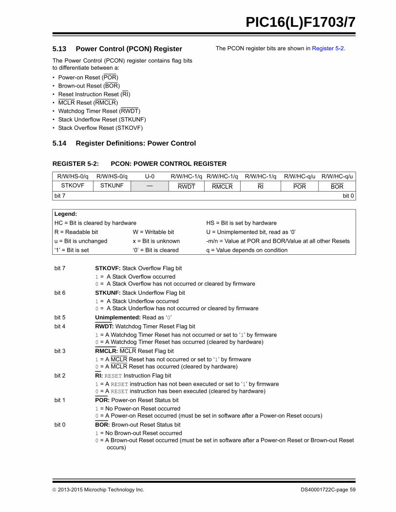
PIC16(L)F1703/7
5.13 Power Control (PCON) Register
The Power Control (PCON) register contains flag bitsto differentiate between a:
• Power-on Reset (POR)
• Brown-out Reset (BOR)
• Reset Instruction Reset (RI)
• MCLR Reset (RMCLR)
• Watchdog Timer Reset (RWDT)
• Stack Underflow Reset (STKUNF)
• Stack Overflow Reset (STKOVF)
The PCON register bits are shown in Register 5-2.
5.14 Register Definitions: Power Control
REGISTER 5-2: PCON: POWER CONTROL REGISTER
R/W/HS-0/q R/W/HS-0/q U-0 R/W/HC-1/q R/W/HC-1/q R/W/HC-1/q R/W/HC-q/u R/W/HC-q/u
STKOVF STKUNF — RWDT RMCLR RI POR BOR
bit 7 bit 0
Legend:
HC = Bit is cleared by hardware HS = Bit is set by hardware
R = Readable bit W = Writable bit U = Unimplemented bit, read as ‘0’
u = Bit is unchanged x = Bit is unknown -m/n = Value at POR and BOR/Value at all other Resets
‘1’ = Bit is set ‘0’ = Bit is cleared q = Value depends on condition
bit 7 STKOVF: Stack Overflow Flag bit
1 = A Stack Overflow occurred0 = A Stack Overflow has not occurred or cleared by firmware
bit 6 STKUNF: Stack Underflow Flag bit
1 = A Stack Underflow occurred0 = A Stack Underflow has not occurred or cleared by firmware
bit 5 Unimplemented: Read as ‘0’
bit 4 RWDT: Watchdog Timer Reset Flag bit
1 = A Watchdog Timer Reset has not occurred or set to ‘1’ by firmware0 = A Watchdog Timer Reset has occurred (cleared by hardware)
bit 3 RMCLR: MCLR Reset Flag bit
1 = A MCLR Reset has not occurred or set to ‘1’ by firmware0 = A MCLR Reset has occurred (cleared by hardware)
bit 2 RI: RESET Instruction Flag bit
1 = A RESET instruction has not been executed or set to ‘1’ by firmware0 = A RESET instruction has been executed (cleared by hardware)
bit 1 POR: Power-on Reset Status bit
1 = No Power-on Reset occurred0 = A Power-on Reset occurred (must be set in software after a Power-on Reset occurs)
bit 0 BOR: Brown-out Reset Status bit
1 = No Brown-out Reset occurred0 = A Brown-out Reset occurred (must be set in software after a Power-on Reset or Brown-out Reset
occurs)
2013-2015 Microchip Technology Inc. DS40001722C-page 59
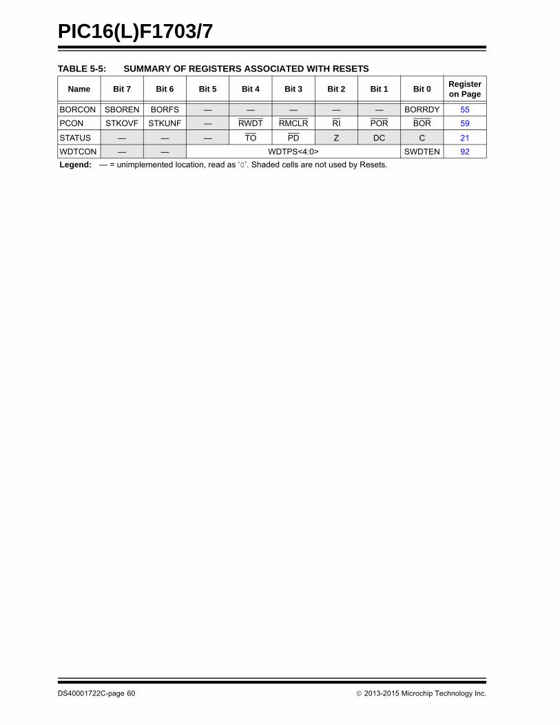
PIC16(L)F1703/7
TABLE 5-5: SUMMARY OF REGISTERS ASSOCIATED WITH RESETS
Name Bit 7 Bit 6 Bit 5 Bit 4 Bit 3 Bit 2 Bit 1 Bit 0Register on Page
BORCON SBOREN BORFS — — — — — BORRDY 55
PCON STKOVF STKUNF — RWDT RMCLR RI POR BOR 59
STATUS — — — TO PD Z DC C 21
WDTCON — — WDTPS<4:0> SWDTEN 92
Legend: — = unimplemented location, read as ‘0’. Shaded cells are not used by Resets.
DS40001722C-page 60 2013-2015 Microchip Technology Inc.
PIC16(L)F1703/7
6.0 OSCILLATOR MODULE (WITH FAIL-SAFE CLOCK MONITOR)
6.1 Overview
The oscillator module has a limited variety of clocksources and selection features that allow it to be usedin applications while maximizing performance and min-imizing power consumption. Figure 6-1 illustrates ablock diagram of the oscillator module.
Clock sources can be supplied from external oscillators,or one of two internal oscillators and PLL circuits, with achoice of speeds selectable via software. Additionalclock features include:
• Selectable system clock source between external or internal sources via software.
The oscillator module can be configured in one of thefollowing clock modes.
1. ECL – External Clock Low-Power mode(0 MHz to 0.5 MHz)
2. ECM – External Clock Medium Power mode(0.5 MHz to 4 MHz)
3. ECH – External Clock High-Power mode(4 MHz to 32 MHz)
4. INTOSC – Internal oscillator (31 kHz to 32 MHz)
Clock Source modes are selected by the FOSC<1:0>bits in the Configuration Words. The FOSC bitsdetermine the type of oscillator that will be used whenthe device is first powered.
The ECH, ECM, and ECL clock modes rely on anexternal logic level signal as the device clock source.Each mode is optimized for a different frequency range.
The INTOSC internal oscillator block produces low,medium, and high-frequency clock sources,designated LFINTOSC, MFINTOSC and HFINTOSC.(see Internal Oscillator Block, Figure 6-1). A wideselection of device clock frequencies may be derivedfrom these three clock sources.
2013-2015 Microchip Technology Inc. DS40001722C-page 61
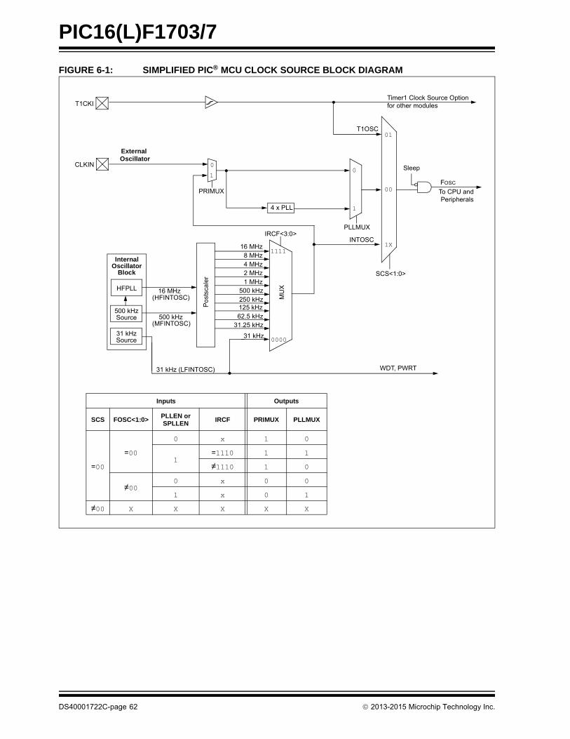
PIC16(L)F1703/7
FIGURE 6-1: SIMPLIFIED PIC® MCU CLOCK SOURCE BLOCK DIAGRAM
Timer1 Clock Source Option for other modules
CLKIN
T1OSC
To CPU and
Po
stsc
ale
r
MU
X
16 MHz8 MHz4 MHz2 MHz1 MHz
250 kHz500 kHz
IRCF<3:0>
31 kHz
500 kHzSource
InternalOscillator
Block
WDT, PWRT
16 MHz
INTOSC
(HFINTOSC)
SCS<1:0>
HFPLL
31 kHz (LFINTOSC)
Oscillator
31 kHzSource
500 kHz(MFINTOSC)
125 kHz
31.25 kHz62.5 kHz
Peripherals
Sleep
External
4 x PLL
1X
01
00
1
00
1
PRIMUX
PLLMUX
0000
1111
Inputs Outputs
SCS FOSC<1:0>PLLEN orSPLLEN
IRCF PRIMUX PLLMUX
=00
=00
0 x 1 0
1=1110 1 1
≠1110 1 0
≠000 x 0 0
1 x 0 1
≠00 X X X X X
FOSC
T1CKI
DS40001722C-page 62 2013-2015 Microchip Technology Inc.
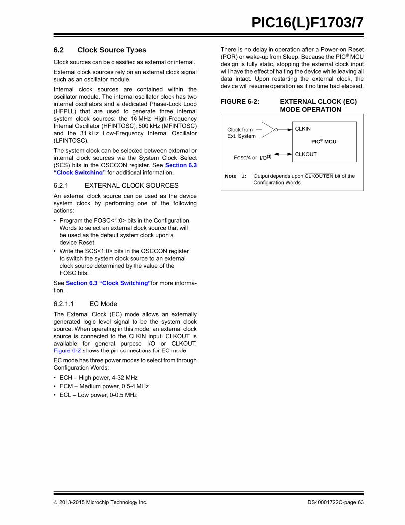
PIC16(L)F1703/7
6.2 Clock Source Types
Clock sources can be classified as external or internal.
External clock sources rely on an external clock signalsuch as an oscillator module.
Internal clock sources are contained within theoscillator module. The internal oscillator block has twointernal oscillators and a dedicated Phase-Lock Loop(HFPLL) that are used to generate three internalsystem clock sources: the 16 MHz High-FrequencyInternal Oscillator (HFINTOSC), 500 kHz (MFINTOSC)and the 31 kHz Low-Frequency Internal Oscillator(LFINTOSC).
The system clock can be selected between external orinternal clock sources via the System Clock Select(SCS) bits in the OSCCON register. See Section 6.3“Clock Switching” for additional information.
6.2.1 EXTERNAL CLOCK SOURCES
An external clock source can be used as the devicesystem clock by performing one of the followingactions:
• Program the FOSC<1:0> bits in the Configuration Words to select an external clock source that will be used as the default system clock upon a device Reset.
• Write the SCS<1:0> bits in the OSCCON register to switch the system clock source to an external clock source determined by the value of the FOSC bits.
See Section 6.3 “Clock Switching”for more informa-tion.
6.2.1.1 EC Mode
The External Clock (EC) mode allows an externallygenerated logic level signal to be the system clocksource. When operating in this mode, an external clocksource is connected to the CLKIN input. CLKOUT isavailable for general purpose I/O or CLKOUT.Figure 6-2 shows the pin connections for EC mode.
EC mode has three power modes to select from throughConfiguration Words:
• ECH – High power, 4-32 MHz
• ECM – Medium power, 0.5-4 MHz
• ECL – Low power, 0-0.5 MHz
There is no delay in operation after a Power-on Reset(POR) or wake-up from Sleep. Because the PIC® MCUdesign is fully static, stopping the external clock inputwill have the effect of halting the device while leaving alldata intact. Upon restarting the external clock, thedevice will resume operation as if no time had elapsed.
FIGURE 6-2: EXTERNAL CLOCK (EC) MODE OPERATION
CLKIN
CLKOUT
Clock fromExt. System
PIC® MCU
FOSC/4 or I/O(1)
Note 1: Output depends upon CLKOUTEN bit of the Configuration Words.
2013-2015 Microchip Technology Inc. DS40001722C-page 63
PIC16(L)F1703/7
6.2.1.2 4x PLL
The oscillator module contains a 4x PLL that can beused with both external and internal clock sources toprovide a system clock source. The input frequency forthe 4x PLL must fall within specifications. See the PLLClock Timing Specifications in Table 26-9.
The 4x PLL may be enabled for use by one of twomethods:
1. Program the PLLEN bit in Configuration Wordsto a ‘1’.
2. Write the SPLLEN bit in the OSCCON register toa ‘1’. If the PLLEN bit in Configuration Words isprogrammed to a ‘1’, then the value of SPLLENis ignored.
6.2.2 INTERNAL CLOCK SOURCES
The device may be configured to use the internaloscillator block as the system clock by performing oneof the following actions:
• Program the FOSC<1:0> bits in Configuration Words to select the INTOSC clock source, which will be used as the default system clock upon a device Reset.
• Write the SCS<1:0> bits in the OSCCON register to switch the system clock source to the internal oscillator during run-time. See Section 6.3 “Clock Switching” for more information.
In INTOSC mode, CLKIN is available for generalpurpose I/O. CLKOUT is available for general purposeI/O or CLKOUT.
The function of the CLKOUT pin is determined by theCLKOUTEN bit in Configuration Words.
The internal oscillator block has two independentoscillators and a dedicated Phase-Lock Loop, HFPLLthat can produce one of three internal system clocksources.
1. The HFINTOSC (High-Frequency InternalOscillator) is factory calibrated and operates at16 MHz. The HFINTOSC source is generatedfrom the 500 kHz MFINTOSC source and thededicated Phase-Lock Loop, HFPLL. Thefrequency of the HFINTOSC can beuser-adjusted via software using the OSCTUNEregister (Register 6-3).
2. The MFINTOSC (Medium-Frequency InternalOscillator) is factory calibrated and operates at500 kHz. The frequency of the MFINTOSC canbe user-adjusted via software using theOSCTUNE register (Register 6-3).
3. The LFINTOSC (Low-Frequency InternalOscillator) is uncalibrated and operates at31 kHz.
6.2.2.1 HFINTOSC
The High-Frequency Internal Oscillator (HFINTOSC) isa factory calibrated 16 MHz internal clock source. Thefrequency of the HFINTOSC can be altered viasoftware using the OSCTUNE register (Register 6-3).
The output of the HFINTOSC connects to a postscalerand multiplexer (see Figure 6-1). One of multiplefrequencies derived from the HFINTOSC can beselected via software using the IRCF<3:0> bits of theOSCCON register. See Section 6.2.2.7 “InternalOscillator Clock Switch Timing” for more information.
The HFINTOSC is enabled by:
• Configure the IRCF<3:0> bits of the OSCCON register for the desired HF frequency, and
• FOSC<1:0> = 00, or
• Set the System Clock Source (SCS) bits of the OSCCON register to ‘1x’
A fast start-up oscillator allows internal circuits to powerup and stabilize before switching to HFINTOSC.
The High-Frequency Internal Oscillator Ready bit(HFIOFR) of the OSCSTAT register indicates when theHFINTOSC is running.
The High-Frequency Internal Oscillator Status Lockedbit (HFIOFL) of the OSCSTAT register indicates whenthe HFINTOSC is running within 2% of its final value.
The High-Frequency Internal Oscillator Stable bit(HFIOFS) of the OSCSTAT register indicates when theHFINTOSC is running within 0.5% of its final value.
6.2.2.2 MFINTOSC
The Medium-Frequency Internal Oscillator(MFINTOSC) is a factory calibrated 500 kHz internalclock source. The frequency of the MFINTOSC can bealtered via software using the OSCTUNE register(Register 6-3).
The output of the MFINTOSC connects to a postscalerand multiplexer (see Figure 6-1). One of ninefrequencies derived from the MFINTOSC can beselected via software using the IRCF<3:0> bits of theOSCCON register. See Section 6.2.2.7 “InternalOscillator Clock Switch Timing” for more information.
The MFINTOSC is enabled by:
• Configure the IRCF<3:0> bits of the OSCCON register for the desired HF frequency, and
• FOSC<1:0> = 00, or
• Set the System Clock Source (SCS) bits of the OSCCON register to ‘1x’
The Medium-Frequency Internal Oscillator Ready bit(MFIOFR) of the OSCSTAT register indicates when theMFINTOSC is running.
DS40001722C-page 64 2013-2015 Microchip Technology Inc.
PIC16(L)F1703/7
6.2.2.3 Internal Oscillator Frequency Adjustment
The 500 kHz internal oscillator is factory calibrated.This internal oscillator can be adjusted in software bywriting to the OSCTUNE register (Register 6-3). Sincethe HFINTOSC and MFINTOSC clock sources arederived from the 500 kHz internal oscillator a change inthe OSCTUNE register value will apply to both.
The default value of the OSCTUNE register is ‘0’. Thevalue is a 6-bit two’s complement number. A value of1Fh will provide an adjustment to the maximumfrequency. A value of 20h will provide an adjustment tothe minimum frequency.
When the OSCTUNE register is modified, the oscillatorfrequency will begin shifting to the new frequency. Codeexecution continues during this shift. There is noindication that the shift has occurred.
OSCTUNE does not affect the LFINTOSC frequency.Operation of features that depend on the LFINTOSCclock source frequency, such as the Power-up Timer(PWRT), Watchdog Timer (WDT), Fail-Safe ClockMonitor (FSCM) and peripherals, are not affected by thechange in frequency.
6.2.2.4 LFINTOSC
The Low-Frequency Internal Oscillator (LFINTOSC) isan uncalibrated 31 kHz internal clock source.
The output of the LFINTOSC connects to a multiplexer(see Figure 6-1). Select 31 kHz, via software, using theIRCF<3:0> bits of the OSCCON register. SeeSection 6.2.2.7 “Internal Oscillator Clock SwitchTiming” for more information. The LFINTOSC is alsothe frequency for the Power-up Timer (PWRT),Watchdog Timer (WDT) and Fail-Safe Clock Monitor(FSCM).
The LFINTOSC is enabled by selecting 31 kHz(IRCF<3:0> bits of the OSCCON register = 000) as thesystem clock source (SCS bits of the OSCCONregister = 1x), or when any of the following areenabled:
• Configure the IRCF<3:0> bits of the OSCCON register for the desired LF frequency, and
• FOSC<1:0> = 00, or
• Set the System Clock Source (SCS) bits of the OSCCON register to ‘1x’
Peripherals that use the LFINTOSC are:
• Power-up Timer (PWRT)
• Watchdog Timer (WDT)
• Fail-Safe Clock Monitor (FSCM)
The Low-Frequency Internal Oscillator Ready bit(LFIOFR) of the OSCSTAT register indicates when theLFINTOSC is running.
6.2.2.5 Internal Oscillator Frequency Selection
The system clock speed can be selected via softwareusing the Internal Oscillator Frequency Select bitsIRCF<3:0> of the OSCCON register.
The postscaled output of the 16 MHz HFINTOSC,500 kHz MFINTOSC, and 31 kHz LFINTOSC connectto a multiplexer (see Figure 6-1). The Internal OscillatorFrequency Select bits IRCF<3:0> of the OSCCONregister select the frequency output of the internaloscillators. One of the following frequencies can beselected via software:
- 32 MHz (requires 4x PLL)
- 16 MHz
- 8 MHz
- 4 MHz
- 2 MHz
- 1 MHz
- 500 kHz (default after Reset)
- 250 kHz
- 125 kHz
- 62.5 kHz
- 31.25 kHz
- 31 kHz (LFINTOSC)
The IRCF<3:0> bits of the OSCCON register allowduplicate selections for some frequencies. Theseduplicate choices can offer system design trade-offs.Lower power consumption can be obtained whenchanging oscillator sources for a given frequency.Faster transition times can be obtained betweenfrequency changes that use the same oscillator source.
Note: Following any Reset, the IRCF<3:0> bitsof the OSCCON register are set to ‘0111’and the frequency selection is set to500 kHz. The user can modify the IRCFbits to select a different frequency.
2013-2015 Microchip Technology Inc. DS40001722C-page 65
PIC16(L)F1703/7
6.2.2.6 32 MHz Internal Oscillator Frequency Selection
The Internal Oscillator Block can be used with the4x PLL associated with the External Oscillator Block toproduce a 32 MHz internal system clock source. Thefollowing settings are required to use the 32 MHzinternal clock source:
• The FOSC bits in Configuration Words must be set to use the INTOSC source as the device system clock (FOSC<1:0> = 00).
• The SCS bits in the OSCCON register must be cleared to use the clock determined by FOSC<1:0> in Configuration Words (SCS<1:0> = 00).
• The IRCF bits in the OSCCON register must be set to the 8 MHz HFINTOSC set to use (IRCF<3:0> = 1110).
• The SPLLEN bit in the OSCCON register must be set to enable the 4x PLL, or the PLLEN bit of the Configuration Words must be programmed to a ‘1’.
The 4x PLL is not available for use with the internaloscillator when the SCS bits of the OSCCON registerare set to ‘1x’. The SCS bits must be set to ‘00’ to usethe 4x PLL with the internal oscillator.
6.2.2.7 Internal Oscillator Clock Switch Timing
When switching between the HFINTOSC, MFINTOSCand the LFINTOSC, the new oscillator may already beshut down to save power (see Figure 6-3). If this is thecase, there is a delay after the IRCF<3:0> bits of theOSCCON register are modified before the frequencyselection takes place. The OSCSTAT register willreflect the current active status of the HFINTOSC,MFINTOSC and LFINTOSC oscillators. The sequenceof a frequency selection is as follows:
1. IRCF<3:0> bits of the OSCCON register aremodified.
2. If the new clock is shut down, a clock start-updelay is started.
3. Clock switch circuitry waits for a falling edge ofthe current clock.
4. The current clock is held low and the clockswitch circuitry waits for a rising edge in the newclock.
5. The new clock is now active.
6. The OSCSTAT register is updated as required.
7. Clock switch is complete.
See Figure 6-3 for more details.
If the internal oscillator speed is switched between twoclocks of the same source, there is no start-up delaybefore the new frequency is selected. Clock switchingtime delays are shown in Table 6-1.
Start-up delay specifications are located in theoscillator tables of Section 26.0 “ElectricalSpecifications”.
Note: When using the PLLEN bit of theConfiguration Words, the 4x PLL cannotbe disabled by software and the SPLLENoption will not be available.
DS40001722C-page 66 2013-2015 Microchip Technology Inc.
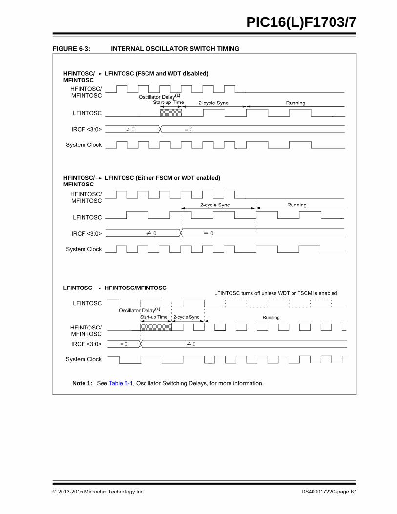
PIC16(L)F1703/7
FIGURE 6-3: INTERNAL OSCILLATOR SWITCH TIMING
HFINTOSC/
LFINTOSC
IRCF <3:0>
System Clock
HFINTOSC/
LFINTOSC
IRCF <3:0>
System Clock
0 0
0 0
Start-up Time 2-cycle Sync Running
2-cycle Sync Running
HFINTOSC/ LFINTOSC (FSCM and WDT disabled)
HFINTOSC/ LFINTOSC (Either FSCM or WDT enabled)
LFINTOSC
HFINTOSC/
IRCF <3:0>
System Clock
= 0 0
Start-up Time 2-cycle Sync Running
LFINTOSC HFINTOSC/MFINTOSCLFINTOSC turns off unless WDT or FSCM is enabled
MFINTOSC
MFINTOSC
MFINTOSC
MFINTOSC
MFINTOSC
Oscillator Delay(1)
Oscillator Delay(1)
Note 1: See Table 6-1, Oscillator Switching Delays, for more information.
2013-2015 Microchip Technology Inc. DS40001722C-page 67
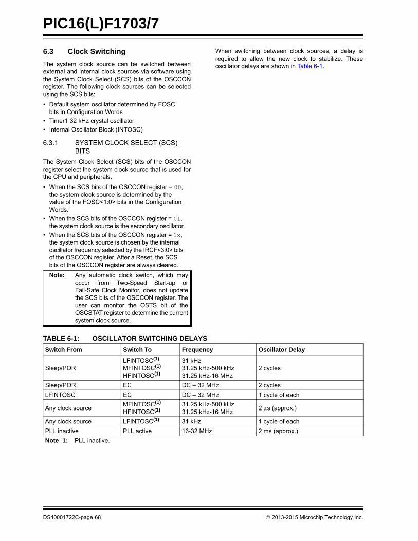
PIC16(L)F1703/7
6.3 Clock Switching
The system clock source can be switched betweenexternal and internal clock sources via software usingthe System Clock Select (SCS) bits of the OSCCONregister. The following clock sources can be selectedusing the SCS bits:
• Default system oscillator determined by FOSC bits in Configuration Words
• Timer1 32 kHz crystal oscillator
• Internal Oscillator Block (INTOSC)
6.3.1 SYSTEM CLOCK SELECT (SCS) BITS
The System Clock Select (SCS) bits of the OSCCONregister select the system clock source that is used forthe CPU and peripherals.
• When the SCS bits of the OSCCON register = 00, the system clock source is determined by the value of the FOSC<1:0> bits in the Configuration Words.
• When the SCS bits of the OSCCON register = 01, the system clock source is the secondary oscillator.
• When the SCS bits of the OSCCON register = 1x, the system clock source is chosen by the internal oscillator frequency selected by the IRCF<3:0> bits of the OSCCON register. After a Reset, the SCS bits of the OSCCON register are always cleared.
When switching between clock sources, a delay isrequired to allow the new clock to stabilize. Theseoscillator delays are shown in Table 6-1.
TABLE 6-1: OSCILLATOR SWITCHING DELAYS
Note: Any automatic clock switch, which mayoccur from Two-Speed Start-up orFail-Safe Clock Monitor, does not updatethe SCS bits of the OSCCON register. Theuser can monitor the OSTS bit of theOSCSTAT register to determine the currentsystem clock source.
Switch From Switch To Frequency Oscillator Delay
Sleep/PORLFINTOSC(1)
MFINTOSC(1)
HFINTOSC(1)
31 kHz31.25 kHz-500 kHz31.25 kHz-16 MHz
2 cycles
Sleep/POR EC DC – 32 MHz 2 cycles
LFINTOSC EC DC – 32 MHz 1 cycle of each
Any clock sourceMFINTOSC(1)
HFINTOSC(1)31.25 kHz-500 kHz31.25 kHz-16 MHz
2 s (approx.)
Any clock source LFINTOSC(1) 31 kHz 1 cycle of each
PLL inactive PLL active 16-32 MHz 2 ms (approx.)
Note 1: PLL inactive.
DS40001722C-page 68 2013-2015 Microchip Technology Inc.
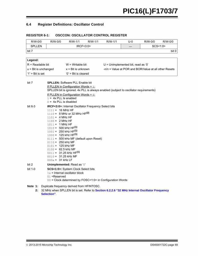
PIC16(L)F1703/7
6.4 Register Definitions: Oscillator Control
REGISTER 6-1: OSCCON: OSCILLATOR CONTROL REGISTER
R/W-0/0 R/W-0/0 R/W-1/1 R/W-1/1 R/W-1/1 U-0 R/W-0/0 R/W-0/0
SPLLEN IRCF<3:0> — SCS<1:0>
bit 7 bit 0
Legend:
R = Readable bit W = Writable bit U = Unimplemented bit, read as ‘0’
u = Bit is unchanged x = Bit is unknown -n/n = Value at POR and BOR/Value at all other Resets
‘1’ = Bit is set ‘0’ = Bit is cleared
bit 7 SPLLEN: Software PLL Enable bitIf PLLEN in Configuration Words = 1:SPLLEN bit is ignored. 4x PLL is always enabled (subject to oscillator requirements)
If PLLEN in Configuration Words = 0:1 = 4x PLL Is enabled0 = 4x PLL is disabled
bit 6-3 IRCF<3:0>: Internal Oscillator Frequency Select bits1111 = 16 MHz HF1110 = 8 MHz or 32 MHz HF(2)
1101 = 4 MHz HF1100 = 2 MHz HF1011 = 1 MHz HF1010 = 500 kHz HF(1)
1001 = 250 kHz HF(1)
1000 = 125 kHz HF(1)
0111 = 500 kHz MF (default upon Reset)0110 = 250 kHz MF0101 = 125 kHz MF0100 = 62.5 kHz MF0011 = 31.25 kHz HF(1)
0010 = 31.25 kHz MF000x = 31 kHz LF
bit 2 Unimplemented: Read as ‘0’
bit 1-0 SCS<1:0>: System Clock Select bits1x = Internal oscillator block01 =Reserved00 = Clock determined by FOSC<1:0> in Configuration Words
Note 1: Duplicate frequency derived from HFINTOSC.
2: 32 MHz when SPLLEN bit is set. Refer to Section 6.2.2.6 “32 MHz Internal Oscillator Frequency Selection”.
2013-2015 Microchip Technology Inc. DS40001722C-page 69
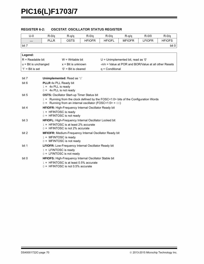
PIC16(L)F1703/7
REGISTER 6-2: OSCSTAT: OSCILLATOR STATUS REGISTER
U-0 R-0/q R-q/q R-0/q R-0/q R-q/q R-0/0 R-0/q
— PLLR OSTS HFIOFR HFIOFL MFIOFR LFIOFR HFIOFS
bit 7 bit 0
Legend:
R = Readable bit W = Writable bit U = Unimplemented bit, read as ‘0’
u = Bit is unchanged x = Bit is unknown -n/n = Value at POR and BOR/Value at all other Resets
‘1’ = Bit is set ‘0’ = Bit is cleared q = Conditional
bit 7 Unimplemented: Read as ‘0’
bit 6 PLLR 4x PLL Ready bit1 = 4x PLL is ready0 = 4x PLL is not ready
bit 5 OSTS: Oscillator Start-up Timer Status bit
1 = Running from the clock defined by the FOSC<1:0> bits of the Configuration Words0 = Running from an internal oscillator (FOSC<1:0> = 00)
bit 4 HFIOFR: High-Frequency Internal Oscillator Ready bit
1 = HFINTOSC is ready0 = HFINTOSC is not ready
bit 3 HFIOFL: High-Frequency Internal Oscillator Locked bit
1 = HFINTOSC is at least 2% accurate0 = HFINTOSC is not 2% accurate
bit 2 MFIOFR: Medium-Frequency Internal Oscillator Ready bit
1 = MFINTOSC is ready 0 = MFINTOSC is not ready
bit 1 LFIOFR: Low-Frequency Internal Oscillator Ready bit
1 = LFINTOSC is ready0 = LFINTOSC is not ready
bit 0 HFIOFS: High-Frequency Internal Oscillator Stable bit
1 = HFINTOSC is at least 0.5% accurate0 = HFINTOSC is not 0.5% accurate
DS40001722C-page 70 2013-2015 Microchip Technology Inc.
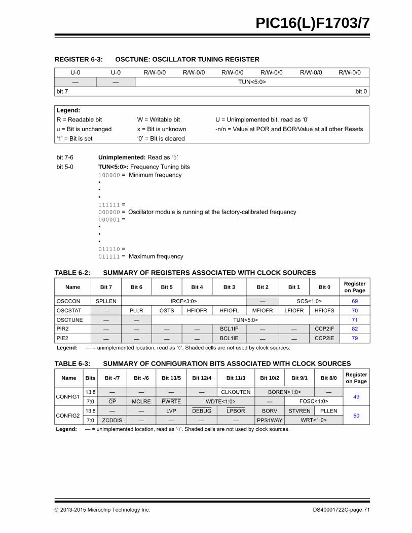
PIC16(L)F1703/7
TABLE 6-2: SUMMARY OF REGISTERS ASSOCIATED WITH CLOCK SOURCES
TABLE 6-3: SUMMARY OF CONFIGURATION BITS ASSOCIATED WITH CLOCK SOURCES
REGISTER 6-3: OSCTUNE: OSCILLATOR TUNING REGISTER
U-0 U-0 R/W-0/0 R/W-0/0 R/W-0/0 R/W-0/0 R/W-0/0 R/W-0/0
— — TUN<5:0>
bit 7 bit 0
Legend:
R = Readable bit W = Writable bit U = Unimplemented bit, read as ‘0’
u = Bit is unchanged x = Bit is unknown -n/n = Value at POR and BOR/Value at all other Resets
‘1’ = Bit is set ‘0’ = Bit is cleared
bit 7-6 Unimplemented: Read as ‘0’
bit 5-0 TUN<5:0>: Frequency Tuning bits100000 = Minimum frequency•••111111 = 000000 = Oscillator module is running at the factory-calibrated frequency000001 = •••011110 = 011111 = Maximum frequency
Name Bit 7 Bit 6 Bit 5 Bit 4 Bit 3 Bit 2 Bit 1 Bit 0Register on Page
OSCCON SPLLEN IRCF<3:0> — SCS<1:0> 69
OSCSTAT — PLLR OSTS HFIOFR HFIOFL MFIOFR LFIOFR HFIOFS 70
OSCTUNE — — TUN<5:0> 71
PIR2 — — — — BCL1IF — — CCP2IF 82
PIE2 — — — — BCL1IE — — CCP2IE 79
Legend: — = unimplemented location, read as ‘0’. Shaded cells are not used by clock sources.
Name Bits Bit -/7 Bit -/6 Bit 13/5 Bit 12/4 Bit 11/3 Bit 10/2 Bit 9/1 Bit 8/0Register on Page
CONFIG113:8 — — — — CLKOUTEN BOREN<1:0> —
497:0 CP MCLRE PWRTE WDTE<1:0> — FOSC<1:0>
CONFIG213:8 — — LVP DEBUG LPBOR BORV STVREN PLLEN
507:0 ZCDDIS — — — — PPS1WAY WRT<1:0>
Legend: — = unimplemented location, read as ‘0’. Shaded cells are not used by clock sources.
2013-2015 Microchip Technology Inc. DS40001722C-page 71
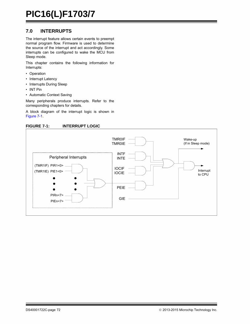
PIC16(L)F1703/7
7.0 INTERRUPTS
The interrupt feature allows certain events to preemptnormal program flow. Firmware is used to determinethe source of the interrupt and act accordingly. Someinterrupts can be configured to wake the MCU fromSleep mode.
This chapter contains the following information forInterrupts:
• Operation
• Interrupt Latency
• Interrupts During Sleep
• INT Pin
• Automatic Context Saving
Many peripherals produce interrupts. Refer to thecorresponding chapters for details.
A block diagram of the interrupt logic is shown inFigure 7-1.
FIGURE 7-1: INTERRUPT LOGIC
TMR0IFTMR0IE
INTFINTE
IOCIFIOCIE
Interruptto CPU
Wake-up (If in Sleep mode)
GIE
(TMR1IF) PIR1<0>
PIRn<7>
PEIE
(TMR1IE) PIE1<0>
Peripheral Interrupts
PIEn<7>
DS40001722C-page 72 2013-2015 Microchip Technology Inc.
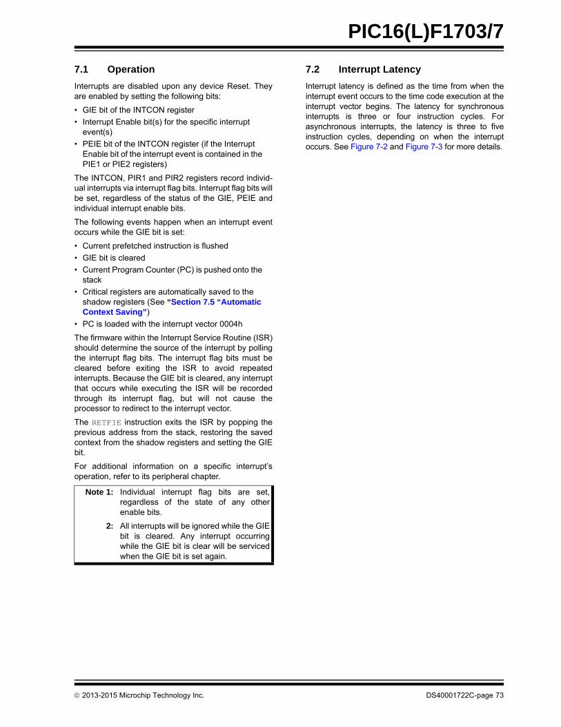
PIC16(L)F1703/7
7.1 Operation
Interrupts are disabled upon any device Reset. Theyare enabled by setting the following bits:
• GIE bit of the INTCON register
• Interrupt Enable bit(s) for the specific interrupt event(s)
• PEIE bit of the INTCON register (if the Interrupt Enable bit of the interrupt event is contained in the PIE1 or PIE2 registers)
The INTCON, PIR1 and PIR2 registers record individ-ual interrupts via interrupt flag bits. Interrupt flag bits willbe set, regardless of the status of the GIE, PEIE andindividual interrupt enable bits.
The following events happen when an interrupt eventoccurs while the GIE bit is set:
• Current prefetched instruction is flushed
• GIE bit is cleared
• Current Program Counter (PC) is pushed onto the stack
• Critical registers are automatically saved to the shadow registers (See “Section 7.5 “Automatic Context Saving”)
• PC is loaded with the interrupt vector 0004h
The firmware within the Interrupt Service Routine (ISR)should determine the source of the interrupt by pollingthe interrupt flag bits. The interrupt flag bits must becleared before exiting the ISR to avoid repeatedinterrupts. Because the GIE bit is cleared, any interruptthat occurs while executing the ISR will be recordedthrough its interrupt flag, but will not cause theprocessor to redirect to the interrupt vector.
The RETFIE instruction exits the ISR by popping theprevious address from the stack, restoring the savedcontext from the shadow registers and setting the GIEbit.
For additional information on a specific interrupt’soperation, refer to its peripheral chapter.
7.2 Interrupt Latency
Interrupt latency is defined as the time from when theinterrupt event occurs to the time code execution at theinterrupt vector begins. The latency for synchronousinterrupts is three or four instruction cycles. Forasynchronous interrupts, the latency is three to fiveinstruction cycles, depending on when the interruptoccurs. See Figure 7-2 and Figure 7-3 for more details.
Note 1: Individual interrupt flag bits are set,regardless of the state of any otherenable bits.
2: All interrupts will be ignored while the GIEbit is cleared. Any interrupt occurringwhile the GIE bit is clear will be servicedwhen the GIE bit is set again.
2013-2015 Microchip Technology Inc. DS40001722C-page 73
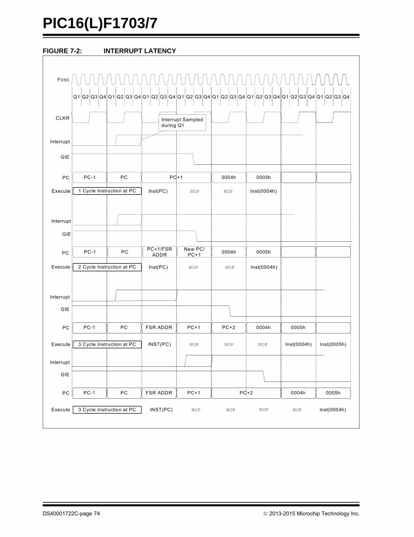
PIC16(L)F1703/7
FIGURE 7-2: INTERRUPT LATENCY
Q1 Q2 Q3 Q4 Q1 Q2 Q3 Q4 Q1 Q2 Q3 Q4 Q1 Q2 Q3 Q4 Q1 Q2 Q3 Q4 Q1 Q2 Q3 Q4
FOSC
CLKR
PC 0004h 0005hPC
Inst(0004h)NOP
GIE
Q1 Q2 Q3 Q4Q1 Q2 Q3 Q4
1 Cycle Instruction at PC
PC
Inst(0004h)NOP2 Cycle Instruction at PC
FSR ADDR PC+1 PC+2 0004h 0005hPC
Inst(0004h)NOP
GIE
PCPC-1
3 Cycle Instruction at PC
Execute
Interrupt
Inst(PC)
Interrupt Sampled during Q1
Inst(PC)
PC-1 PC+1
NOP
PCNew PC/
PC+10005hPC-1
PC+1/FSR ADDR
0004h
NOP
Interrupt
GIE
Interrupt
INST(PC) NOPNOP
FSR ADDR PC+1 PC+2 0004h 0005hPC
Inst(0004h)NOP
GIE
PCPC-1
3 Cycle Instruction at PC
Interrupt
INST(PC) NOPNOP NOP
Inst(0005h)
Execute
Execute
Execute
DS40001722C-page 74 2013-2015 Microchip Technology Inc.
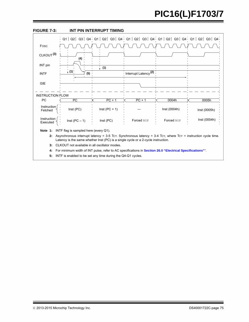
PIC16(L)F1703/7
FIGURE 7-3: INT PIN INTERRUPT TIMING
Q2Q1 Q3 Q4 Q2Q1 Q3 Q4 Q2Q1 Q3 Q4 Q2Q1 Q3 Q4 Q2Q1 Q3 Q4
FOSC
CLKOUT
INT pin
INTF
GIE
INSTRUCTION FLOW
PC
InstructionFetched
InstructionExecuted
Interrupt Latency
PC PC + 1 PC + 1 0004h 0005h
Inst (0004h) Inst (0005h)
Forced NOP
Inst (PC) Inst (PC + 1)
Inst (PC – 1) Inst (0004h) Forced NOPInst (PC)
—
Note 1: INTF flag is sampled here (every Q1).
2: Asynchronous interrupt latency = 3-5 TCY. Synchronous latency = 3-4 TCY, where TCY = instruction cycle time.Latency is the same whether Inst (PC) is a single cycle or a 2-cycle instruction.
3: CLKOUT not available in all oscillator modes.
4: For minimum width of INT pulse, refer to AC specifications in Section 26.0 “Electrical Specifications””.
5: INTF is enabled to be set any time during the Q4-Q1 cycles.
(1)
(2)
(3)
(4)
(5)(1)
2013-2015 Microchip Technology Inc. DS40001722C-page 75
PIC16(L)F1703/7
7.3 Interrupts During Sleep
Some interrupts can be used to wake from Sleep. Towake from Sleep, the peripheral must be able tooperate without the system clock. The interrupt sourcemust have the appropriate Interrupt Enable bit(s) setprior to entering Sleep.
On waking from Sleep, if the GIE bit is also set, theprocessor will branch to the interrupt vector. Otherwise,the processor will continue executing instructions afterthe SLEEP instruction. The instruction directly after theSLEEP instruction will always be executed beforebranching to the ISR. Refer to Section 8.0“Power-Down Mode (Sleep)” for more details.
7.4 INT Pin
The INT pin can be used to generate an asynchronousedge-triggered interrupt. This interrupt is enabled bysetting the INTE bit of the INTCON register. TheINTEDG bit of the OPTION_REG register determines onwhich edge the interrupt will occur. When the INTEDGbit is set, the rising edge will cause the interrupt. Whenthe INTEDG bit is clear, the falling edge will cause theinterrupt. The INTF bit of the INTCON register will be setwhen a valid edge appears on the INT pin. If the GIE andINTE bits are also set, the processor will redirectprogram execution to the interrupt vector.
7.5 Automatic Context Saving
Upon entering an interrupt, the return PC address issaved on the stack. Additionally, the following registersare automatically saved in the shadow registers:
• W register
• STATUS register (except for TO and PD)
• BSR register
• FSR registers
• PCLATH register
Upon exiting the Interrupt Service Routine, these regis-ters are automatically restored. Any modifications tothese registers during the ISR will be lost. If modifica-tions to any of these registers are desired, the corre-sponding shadow register should be modified and thevalue will be restored when exiting the ISR. Theshadow registers are available in Bank 31 and arereadable and writable. Depending on the user’sapplication, other registers may also need to be saved.
DS40001722C-page 76 2013-2015 Microchip Technology Inc.

PIC16(L)F1703/7
7.6 Register Definitions: Interrupt Control
REGISTER 7-1: INTCON: INTERRUPT CONTROL REGISTER
R/W-0/0 R/W-0/0 R/W-0/0 R/W-0/0 R/W-0/0 R/W-0/0 R/W-0/0 R-0/0
GIE PEIE TMR0IE INTE IOCIE TMR0IF INTF IOCIF(1)
bit 7 bit 0
Legend:
R = Readable bit W = Writable bit U = Unimplemented bit, read as ‘0’
u = Bit is unchanged x = Bit is unknown -n/n = Value at POR and BOR/Value at all other Resets
‘1’ = Bit is set ‘0’ = Bit is cleared
bit 7 GIE: Global Interrupt Enable bit
1 = Enables all active interrupts0 = Disables all interrupts
bit 6 PEIE: Peripheral Interrupt Enable bit1 = Enables all active peripheral interrupts0 = Disables all peripheral interrupts
bit 5 TMR0IE: Timer0 Overflow Interrupt Enable bit1 = Enables the Timer0 interrupt0 = Disables the Timer0 interrupt
bit 4 INTE: INT External Interrupt Enable bit1 = Enables the INT external interrupt0 = Disables the INT external interrupt
bit 3 IOCIE: Interrupt-on-Change Enable bit1 = Enables the interrupt-on-change0 = Disables the interrupt-on-change
bit 2 TMR0IF: Timer0 Overflow Interrupt Flag bit1 = TMR0 register has overflowed0 = TMR0 register did not overflow
bit 1 INTF: INT External Interrupt Flag bit1 = The INT external interrupt occurred0 = The INT external interrupt did not occur
bit 0 IOCIF: Interrupt-on-Change Interrupt Flag bit(1)
1 = When at least one of the interrupt-on-change pins changed state0 = None of the interrupt-on-change pins have changed state
Note 1: The IOCIF Flag bit is read-only and cleared when all the interrupt-on-change flags in the IOCxF registers have been cleared by software.
Note: Interrupt flag bits are set when an interruptcondition occurs, regardless of the state ofits corresponding enable bit or the GlobalEnable bit, GIE, of the INTCON register.User software should ensure theappropriate interrupt flag bits are clearprior to enabling an interrupt.
2013-2015 Microchip Technology Inc. DS40001722C-page 77
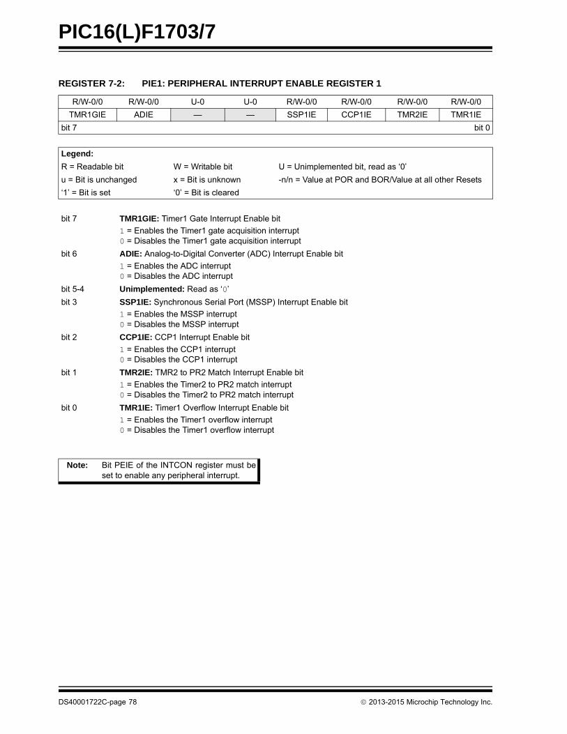
PIC16(L)F1703/7
REGISTER 7-2: PIE1: PERIPHERAL INTERRUPT ENABLE REGISTER 1
R/W-0/0 R/W-0/0 U-0 U-0 R/W-0/0 R/W-0/0 R/W-0/0 R/W-0/0
TMR1GIE ADIE — — SSP1IE CCP1IE TMR2IE TMR1IE
bit 7 bit 0
Legend:
R = Readable bit W = Writable bit U = Unimplemented bit, read as ‘0’
u = Bit is unchanged x = Bit is unknown -n/n = Value at POR and BOR/Value at all other Resets
‘1’ = Bit is set ‘0’ = Bit is cleared
bit 7 TMR1GIE: Timer1 Gate Interrupt Enable bit
1 = Enables the Timer1 gate acquisition interrupt0 = Disables the Timer1 gate acquisition interrupt
bit 6 ADIE: Analog-to-Digital Converter (ADC) Interrupt Enable bit
1 = Enables the ADC interrupt0 = Disables the ADC interrupt
bit 5-4 Unimplemented: Read as ‘0’
bit 3 SSP1IE: Synchronous Serial Port (MSSP) Interrupt Enable bit
1 = Enables the MSSP interrupt0 = Disables the MSSP interrupt
bit 2 CCP1IE: CCP1 Interrupt Enable bit
1 = Enables the CCP1 interrupt0 = Disables the CCP1 interrupt
bit 1 TMR2IE: TMR2 to PR2 Match Interrupt Enable bit
1 = Enables the Timer2 to PR2 match interrupt0 = Disables the Timer2 to PR2 match interrupt
bit 0 TMR1IE: Timer1 Overflow Interrupt Enable bit
1 = Enables the Timer1 overflow interrupt0 = Disables the Timer1 overflow interrupt
Note: Bit PEIE of the INTCON register must beset to enable any peripheral interrupt.
DS40001722C-page 78 2013-2015 Microchip Technology Inc.

PIC16(L)F1703/7
REGISTER 7-3: PIE2: PERIPHERAL INTERRUPT ENABLE REGISTER 2
U-0 U-0 U-0 U-0 R/W-0/0 U-0 U-0 R/W-0/0
— — — — BCL1IE — — CCP2IE
bit 7 bit 0
Legend:
R = Readable bit W = Writable bit U = Unimplemented bit, read as ‘0’
u = Bit is unchanged x = Bit is unknown -n/n = Value at POR and BOR/Value at all other Resets
‘1’ = Bit is set ‘0’ = Bit is cleared
bit 7-4 Unimplemented: Read as ‘0’
bit 3 BCL1IE: MSSP Bus Collision Interrupt Enable bit
1 = Enables the MSSP Bus Collision Interrupt0 = Disables the MSSP Bus Collision Interrupt
bit 2-1 Unimplemented: Read as ‘0’
bit 0 CCP2IE: CCP2 Interrupt Enable bit
1 = Enables the CCP2 interrupt0 = Disables the CCP2 interrupt
Note: Bit PEIE of the INTCON register must beset to enable any peripheral interrupt.
2013-2015 Microchip Technology Inc. DS40001722C-page 79

PIC16(L)F1703/7
REGISTER 7-4: PIE3: PERIPHERAL INTERRUPT ENABLE REGISTER 3
U-0 U-0 U-0 R/W-0/0 U-0 U-0 U-0 U-0
— — — ZCDIE — — — —
bit 7 bit 0
Legend:
R = Readable bit W = Writable bit U = Unimplemented bit, read as ‘0’
u = Bit is unchanged x = Bit is unknown -n/n = Value at POR and BOR/Value at all other Resets
‘1’ = Bit is set ‘0’ = Bit is cleared
bit 7-5 Unimplemented: Read as ‘0’
bit 4 ZCDIE: Zero-Cross Detection Interrupt Enable bit
1 = ZCD interrupt enabled0 = ZCD interrupt disabled
bit 3-0 Unimplemented: Read as ‘0’
Note: Bit PEIE of the INTCON register must beset to enable any peripheral interrupt.
DS40001722C-page 80 2013-2015 Microchip Technology Inc.
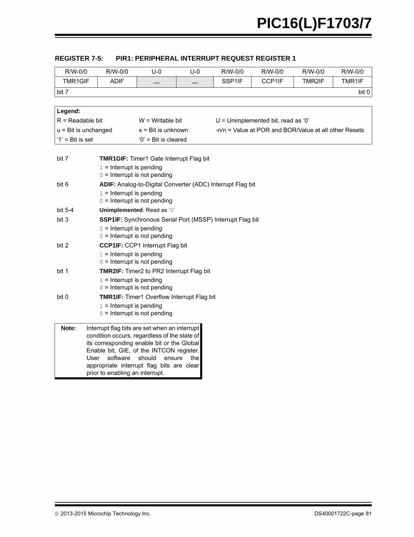
PIC16(L)F1703/7
REGISTER 7-5: PIR1: PERIPHERAL INTERRUPT REQUEST REGISTER 1
R/W-0/0 R/W-0/0 U-0 U-0 R/W-0/0 R/W-0/0 R/W-0/0 R/W-0/0
TMR1GIF ADIF — — SSP1IF CCP1IF TMR2IF TMR1IF
bit 7 bit 0
Legend:
R = Readable bit W = Writable bit U = Unimplemented bit, read as ‘0’
u = Bit is unchanged x = Bit is unknown -n/n = Value at POR and BOR/Value at all other Resets
‘1’ = Bit is set ‘0’ = Bit is cleared
bit 7 TMR1GIF: Timer1 Gate Interrupt Flag bit
1 = Interrupt is pending0 = Interrupt is not pending
bit 6 ADIF: Analog-to-Digital Converter (ADC) Interrupt Flag bit
1 = Interrupt is pending0 = Interrupt is not pending
bit 5-4 Unimplemented: Read as ‘0’
bit 3 SSP1IF: Synchronous Serial Port (MSSP) Interrupt Flag bit
1 = Interrupt is pending0 = Interrupt is not pending
bit 2 CCP1IF: CCP1 Interrupt Flag bit
1 = Interrupt is pending0 = Interrupt is not pending
bit 1 TMR2IF: Timer2 to PR2 Interrupt Flag bit
1 = Interrupt is pending0 = Interrupt is not pending
bit 0 TMR1IF: Timer1 Overflow Interrupt Flag bit
1 = Interrupt is pending0 = Interrupt is not pending
Note: Interrupt flag bits are set when an interruptcondition occurs, regardless of the state ofits corresponding enable bit or the GlobalEnable bit, GIE, of the INTCON register.User software should ensure theappropriate interrupt flag bits are clearprior to enabling an interrupt.
2013-2015 Microchip Technology Inc. DS40001722C-page 81
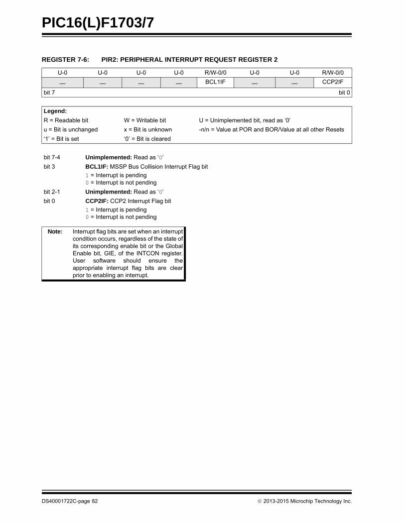
PIC16(L)F1703/7
REGISTER 7-6: PIR2: PERIPHERAL INTERRUPT REQUEST REGISTER 2
U-0 U-0 U-0 U-0 R/W-0/0 U-0 U-0 R/W-0/0
— — — — BCL1IF — — CCP2IF
bit 7 bit 0
Legend:
R = Readable bit W = Writable bit U = Unimplemented bit, read as ‘0’
u = Bit is unchanged x = Bit is unknown -n/n = Value at POR and BOR/Value at all other Resets
‘1’ = Bit is set ‘0’ = Bit is cleared
bit 7-4 Unimplemented: Read as ‘0’
bit 3 BCL1IF: MSSP Bus Collision Interrupt Flag bit
1 = Interrupt is pending0 = Interrupt is not pending
bit 2-1 Unimplemented: Read as ‘0’
bit 0 CCP2IF: CCP2 Interrupt Flag bit
1 = Interrupt is pending0 = Interrupt is not pending
Note: Interrupt flag bits are set when an interruptcondition occurs, regardless of the state ofits corresponding enable bit or the GlobalEnable bit, GIE, of the INTCON register.User software should ensure theappropriate interrupt flag bits are clearprior to enabling an interrupt.
DS40001722C-page 82 2013-2015 Microchip Technology Inc.
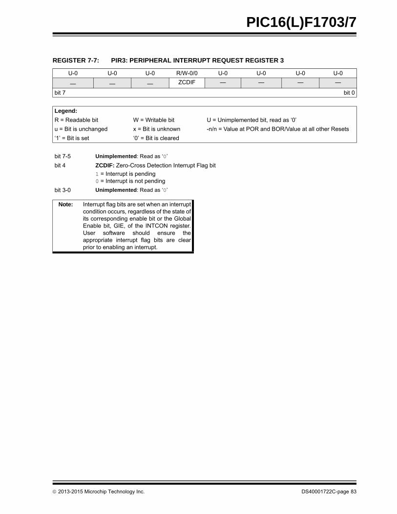
PIC16(L)F1703/7
REGISTER 7-7: PIR3: PERIPHERAL INTERRUPT REQUEST REGISTER 3
U-0 U-0 U-0 R/W-0/0 U-0 U-0 U-0 U-0
— — — ZCDIF — — — —
bit 7 bit 0
Legend:
R = Readable bit W = Writable bit U = Unimplemented bit, read as ‘0’
u = Bit is unchanged x = Bit is unknown -n/n = Value at POR and BOR/Value at all other Resets
‘1’ = Bit is set ‘0’ = Bit is cleared
bit 7-5 Unimplemented: Read as ‘0’
bit 4 ZCDIF: Zero-Cross Detection Interrupt Flag bit
1 = Interrupt is pending0 = Interrupt is not pending
bit 3-0 Unimplemented: Read as ‘0’
Note: Interrupt flag bits are set when an interruptcondition occurs, regardless of the state ofits corresponding enable bit or the GlobalEnable bit, GIE, of the INTCON register.User software should ensure theappropriate interrupt flag bits are clearprior to enabling an interrupt.
2013-2015 Microchip Technology Inc. DS40001722C-page 83
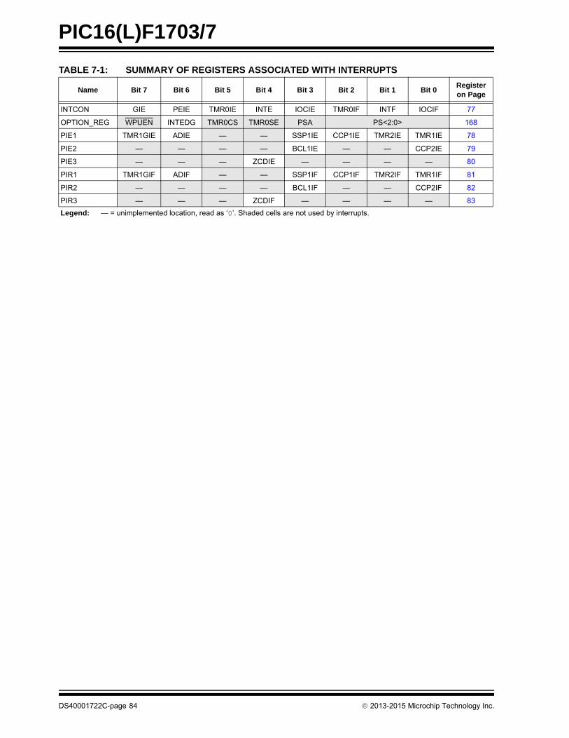
PIC16(L)F1703/7
TABLE 7-1: SUMMARY OF REGISTERS ASSOCIATED WITH INTERRUPTS
Name Bit 7 Bit 6 Bit 5 Bit 4 Bit 3 Bit 2 Bit 1 Bit 0Register on Page
INTCON GIE PEIE TMR0IE INTE IOCIE TMR0IF INTF IOCIF 77
OPTION_REG WPUEN INTEDG TMR0CS TMR0SE PSA PS<2:0> 168
PIE1 TMR1GIE ADIE — — SSP1IE CCP1IE TMR2IE TMR1IE 78
PIE2 — — — — BCL1IE — — CCP2IE 79
PIE3 — — — ZCDIE — — — — 80
PIR1 TMR1GIF ADIF — — SSP1IF CCP1IF TMR2IF TMR1IF 81
PIR2 — — — — BCL1IF — — CCP2IF 82
PIR3 — — — ZCDIF — — — — 83
Legend: — = unimplemented location, read as ‘0’. Shaded cells are not used by interrupts.
DS40001722C-page 84 2013-2015 Microchip Technology Inc.

PIC16(L)F1703/7
8.0 POWER-DOWN MODE (SLEEP)
The Power-down mode is entered by executing aSLEEP instruction.
Upon entering Sleep mode, the following conditionsexist:
1. WDT will be cleared but keeps running, ifenabled for operation during Sleep.
2. PD bit of the STATUS register is cleared.
3. TO bit of the STATUS register is set.
4. CPU clock is disabled.
5. 31 kHz LFINTOSC is unaffected and peripheralsthat operate from it may continue operation inSleep.
6. Timer1 and peripherals that operate fromTimer1 continue operation in Sleep when theTimer1 clock source selected is:
• LFINTOSC
• T1CKI
• Secondary oscillator
7. ADC is unaffected, if the dedicated FRCoscillator is selected.
8. I/O ports maintain the status they had beforeSLEEP was executed (driving high, low orhigh-impedance).
9. Resets other than WDT are not affected bySleep mode.
Refer to individual chapters for more details onperipheral operation during Sleep.
To minimize current consumption, the followingconditions should be considered:
• I/O pins should not be floating
• External circuitry sinking current from I/O pins
• Internal circuitry sourcing current from I/O pins
• Current draw from pins with internal weak pull-ups
• Modules using 31 kHz LFINTOSC
I/O pins that are high-impedance inputs should bepulled to VDD or VSS externally to avoid switchingcurrents caused by floating inputs.
Examples of internal circuitry that might be sourcingcurrent include the FVR module. See Section 14.0“Fixed Voltage Reference (FVR)” for moreinformation on the FVR module.
8.1 Wake-up from Sleep
The device can wake-up from Sleep through one of thefollowing events:
1. External Reset input on MCLR pin, if enabled
2. BOR Reset, if enabled
3. POR Reset
4. Watchdog Timer, if enabled
5. Any external interrupt
6. Interrupts by peripherals capable of runningduring Sleep (see individual peripheral for moreinformation)
The first three events will cause a device Reset. Thelast three events are considered a continuation ofprogram execution. To determine whether a deviceReset or wake-up event occurred, refer toSection 5.12 “Determining the Cause of a Reset”.
When the SLEEP instruction is being executed, the nextinstruction (PC + 1) is prefetched. For the device towake-up through an interrupt event, the correspondinginterrupt enable bit must be enabled. Wake-up willoccur regardless of the state of the GIE bit. If the GIEbit is disabled, the device continues execution at theinstruction after the SLEEP instruction. If the GIE bit isenabled, the device executes the instruction after theSLEEP instruction, the device will then call the InterruptService Routine. In cases where the execution of theinstruction following SLEEP is not desirable, the usershould have a NOP after the SLEEP instruction.
The WDT is cleared when the device wakes up fromSleep, regardless of the source of wake-up.
2013-2015 Microchip Technology Inc. DS40001722C-page 85
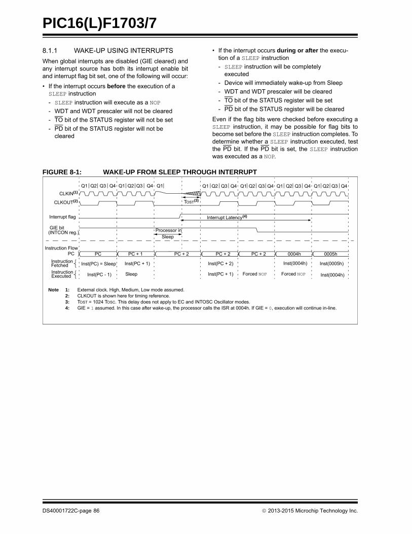
PIC16(L)F1703/7
8.1.1 WAKE-UP USING INTERRUPTS
When global interrupts are disabled (GIE cleared) andany interrupt source has both its interrupt enable bitand interrupt flag bit set, one of the following will occur:
• If the interrupt occurs before the execution of a SLEEP instruction
- SLEEP instruction will execute as a NOP
- WDT and WDT prescaler will not be cleared
- TO bit of the STATUS register will not be set
- PD bit of the STATUS register will not be cleared
• If the interrupt occurs during or after the execu-tion of a SLEEP instruction
- SLEEP instruction will be completely executed
- Device will immediately wake-up from Sleep
- WDT and WDT prescaler will be cleared
- TO bit of the STATUS register will be set
- PD bit of the STATUS register will be cleared
Even if the flag bits were checked before executing aSLEEP instruction, it may be possible for flag bits tobecome set before the SLEEP instruction completes. Todetermine whether a SLEEP instruction executed, testthe PD bit. If the PD bit is set, the SLEEP instructionwas executed as a NOP.
FIGURE 8-1: WAKE-UP FROM SLEEP THROUGH INTERRUPT
Q1 Q2 Q3 Q4 Q1 Q2 Q3 Q4 Q1 Q1 Q2 Q3 Q4 Q1 Q2 Q3 Q4 Q1 Q2 Q3 Q4 Q1 Q2 Q3 Q4
CLKIN(1)
CLKOUT(2)
Interrupt flag
GIE bit(INTCON reg.)
Instruction FlowPC
InstructionFetched
InstructionExecuted
PC PC + 1 PC + 2
Inst(PC) = Sleep
Inst(PC - 1)
Inst(PC + 1)
Sleep
Processor inSleep
Interrupt Latency(4)
Inst(PC + 2)
Inst(PC + 1)
Inst(0004h) Inst(0005h)
Inst(0004h)Forced NOP
PC + 2 0004h 0005h
Forced NOP
TOST(3)
PC + 2
Note 1: External clock. High, Medium, Low mode assumed.2: CLKOUT is shown here for timing reference.3: TOST = 1024 TOSC. This delay does not apply to EC and INTOSC Oscillator modes.4: GIE = 1 assumed. In this case after wake-up, the processor calls the ISR at 0004h. If GIE = 0, execution will continue in-line.
DS40001722C-page 86 2013-2015 Microchip Technology Inc.
PIC16(L)F1703/7
8.2 Low-Power Sleep Mode
The PIC16F1703/7 device contains an internal LowDropout (LDO) voltage regulator, which allows thedevice I/O pins to operate at voltages up to 5.5V whilethe internal device logic operates at a lower voltage.The LDO and its associated reference circuitry mustremain active when the device is in Sleep mode. ThePIC16F1703/7 allows the user to optimize theoperating current in Sleep, depending on theapplication requirements.
A Low-Power Sleep mode can be selected by settingthe VREGPM bit of the VREGCON register. With thisbit set, the LDO and reference circuitry are placed in alow-power state when the device is in Sleep.
8.2.1 SLEEP CURRENT VS. WAKE-UP TIME
In the default operating mode, the LDO and referencecircuitry remain in the normal configuration while inSleep. The device is able to exit Sleep mode quicklysince all circuits remain active. In Low-Power Sleepmode, when waking up from Sleep, an extra delay timeis required for these circuits to return to the normalconfiguration and stabilize.
The Low-Power Sleep mode is beneficial for applica-tions that stay in Sleep mode for long periods of time.The normal mode is beneficial for applications thatneed to wake from Sleep quickly and frequently.
8.2.2 PERIPHERAL USAGE IN SLEEP
Some peripherals that can operate in Sleep mode willnot operate properly with the Low-Power Sleep modeselected. The Low-Power Sleep mode is intended foruse only with the following peripherals:
• Brown-Out Reset (BOR)
• Watchdog Timer (WDT)
• External interrupt pin/Interrupt-on-change pins
• Timer1 (with external clock source < 100 kHz)
Note: The PIC16LF1703/7 does not have aconfigurable Low-Power Sleep mode.PIC16LF1703/7 is an unregulated deviceand is always in the lowest power statewhen in Sleep, with no wake-up timepenalty. This device has a lower maximumVDD and I/O voltage than thePIC16F1703/7. See Section 26.0“Electrical Specifications” for moreinformation.
2013-2015 Microchip Technology Inc. DS40001722C-page 87
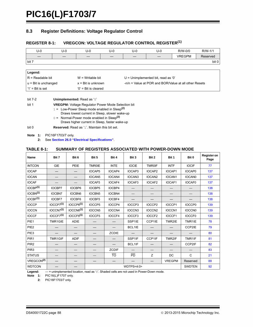
PIC16(L)F1703/7
8.3 Register Definitions: Voltage Regulator Control
TABLE 8-1: SUMMARY OF REGISTERS ASSOCIATED WITH POWER-DOWN MODE
REGISTER 8-1: VREGCON: VOLTAGE REGULATOR CONTROL REGISTER(1)
U-0 U-0 U-0 U-0 U-0 U-0 R/W-0/0 R/W-1/1
— — — — — — VREGPM Reserved
bit 7 bit 0
Legend:
R = Readable bit W = Writable bit U = Unimplemented bit, read as ‘0’
u = Bit is unchanged x = Bit is unknown -n/n = Value at POR and BOR/Value at all other Resets
‘1’ = Bit is set ‘0’ = Bit is cleared
bit 7-2 Unimplemented: Read as ‘0’
bit 1 VREGPM: Voltage Regulator Power Mode Selection bit1 = Low-Power Sleep mode enabled in Sleep(2)
Draws lowest current in Sleep, slower wake-up0 = Normal-Power mode enabled in Sleep(2)
Draws higher current in Sleep, faster wake-up
bit 0 Reserved: Read as ‘1’. Maintain this bit set.
Note 1: PIC16F1703/7 only.2: See Section 26.0 “Electrical Specifications”.
Name Bit 7 Bit 6 Bit 5 Bit 4 Bit 3 Bit 2 Bit 1 Bit 0Register on
Page
INTCON GIE PEIE TMR0IE INTE IOCIE TMR0IF INTF IOCIF 77
IOCAP — — IOCAP5 IOCAP4 IOCAP3 IOCAP2 IOCAP1 IOCAP0 137
IOCAN — — IOCAN5 IOCAN4 IOCAN3 IOCAN2 IOCAN1 IOCAN0 137
IOCAF — — IOCAF5 IOCAF4 IOCAF3 IOCAF2 IOCAF1 IOCAF0 137
IOCBP(1) IOCBP7 IOCBP6 IOCBP5 IOCBP4 — — — — 138
IOCBN(1) IOCBN7 IOCBN6 IOCBN5 IOCBN4 — — — — 138
IOCBF(1) IOCBF7 IOCBF6 IOCBF5 IOCBF4 — — — — 138
IOCCP IOCCP7(1) IOCCP6(1) IOCCP5 IOCCP4 IOCCP3 IOCCP2 IOCCP1 IOCCP0 139
IOCCN IOCCN7(1) IOCCN6(1) IOCCN5 IOCCN4 IOCCN3 IOCCN2 IOCCN1 IOCCN0 139
IOCCF IOCCF7(1) IOCCF6(1) IOCCF5 IOCCF4 IOCCF3 IOCCF2 IOCCF1 IOCCF0 139
PIE1 TMR1GIE ADIE — — SSP1IE CCP1IE TMR2IE TMR1IE 78
PIE2 — — — — BCL1IE — — CCP2IE 79
PIE3 — — — ZCDIE — — — — 80
PIR1 TMR1GIF ADIF — — SSP1IF CCP1IF TMR2IF TMR1IF 81
PIR2 — — — — BCL1IF — — CCP2IF 82
PIR3 — — — ZCDIF — — — — 83
STATUS — — — TO PD Z DC C 21
VREGCON(2) — — — — — — VREGPM Reserved 88
WDTCON — — WDTPS<4:0> SWDTEN 92
Legend: — = unimplemented location, read as ‘0’. Shaded cells are not used in Power-Down mode.Note 1: PIC16(L)F1707 only.
2: PIC16F1703/7 only.
DS40001722C-page 88 2013-2015 Microchip Technology Inc.

PIC16(L)F1703/7
9.0 WATCHDOG TIMER (WDT)
The Watchdog Timer is a system timer that generatesa Reset if the firmware does not issue a CLRWDTinstruction within the time-out period. The WatchdogTimer is typically used to recover the system fromunexpected events.
The WDT has the following features:
• Independent clock source
• Multiple operating modes
- WDT is always on
- WDT is off when in Sleep
- WDT is controlled by software
- WDT is always off
• Configurable time-out period is from 1 ms to 256 seconds (nominal)
• Multiple Reset conditions
• Operation during Sleep
FIGURE 9-1: WATCHDOG TIMER BLOCK DIAGRAM
LFINTOSC23-bit Programmable
Prescaler WDTWDT Time-out
WDTPS<4:0>
SWDTEN
Sleep
WDTE<1:0> = 11
WDTE<1:0> = 01
WDTE<1:0> = 10
2013-2015 Microchip Technology Inc. DS40001722C-page 89

PIC16(L)F1703/7
9.1 Independent Clock Source
The WDT derives its time base from the 31 kHzLFINTOSC internal oscillator. Time intervals in thischapter are based on a nominal interval of 1 ms. SeeTable 26-8 for the LFINTOSC specification.
9.2 WDT Operating Modes
The Watchdog Timer module has four operating modescontrolled by the WDTE<1:0> bits in ConfigurationWords. See Table 9-1.
9.2.1 WDT IS ALWAYS ON
When the WDTE bits of Configuration Words are set to‘11’, the WDT is always on.
WDT protection is active during Sleep.
9.2.2 WDT IS OFF IN SLEEP
When the WDTE bits of Configuration Words are set to‘10’, the WDT is on, except in Sleep.
WDT protection is not active during Sleep.
9.2.3 WDT CONTROLLED BY SOFTWARE
When the WDTE bits of Configuration Words are set to‘01’, the WDT is controlled by the SWDTEN bit of theWDTCON register.
WDT protection is unchanged by Sleep. See Table 9-1for more details.
TABLE 9-1: WDT OPERATING MODES
9.3 Time-Out Period
The WDTPS bits of the WDTCON register set thetime-out period from 1 ms to 256 seconds (nominal).After a Reset, the default time-out period is twoseconds.
9.4 Clearing the WDT
The WDT is cleared when any of the followingconditions occur:
• Any Reset
• CLRWDT instruction is executed
• Device enters Sleep
• Device wakes up from Sleep
• Oscillator fail
• WDT is disabled
• Oscillator Start-up Timer (OST) is running
See Table 9-2 for more information.
9.5 Operation During Sleep
When the device enters Sleep, the WDT is cleared. Ifthe WDT is enabled during Sleep, the WDT resumescounting.
When the device exits Sleep, the WDT is clearedagain. The WDT remains clear until the OST, ifenabled, completes. See Section 6.0 “OscillatorModule (with Fail-Safe Clock Monitor)” for moreinformation on the OST.
When a WDT time-out occurs while the device is inSleep, no Reset is generated. Instead, the devicewakes up and resumes operation. The TO and PD bitsin the STATUS register are changed to indicate theevent. See STATUS Register (Register 3-1) for moreinformation.
WDTE<1:0> SWDTENDevice Mode
WDT Mode
11 X X Active
10 XAwake Active
Sleep Disabled
011
XActive
0 Disabled
00 X X Disabled
DS40001722C-page 90 2013-2015 Microchip Technology Inc.
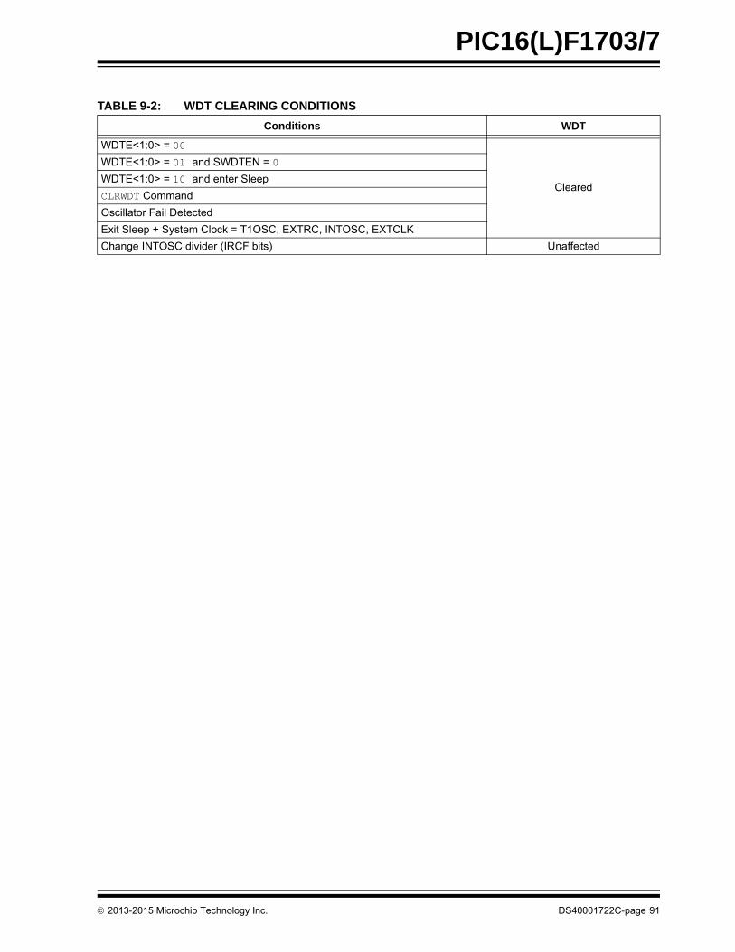
PIC16(L)F1703/7
TABLE 9-2: WDT CLEARING CONDITIONS
Conditions WDT
WDTE<1:0> = 00
Cleared
WDTE<1:0> = 01 and SWDTEN = 0
WDTE<1:0> = 10 and enter Sleep
CLRWDT Command
Oscillator Fail Detected
Exit Sleep + System Clock = T1OSC, EXTRC, INTOSC, EXTCLK
Change INTOSC divider (IRCF bits) Unaffected
2013-2015 Microchip Technology Inc. DS40001722C-page 91
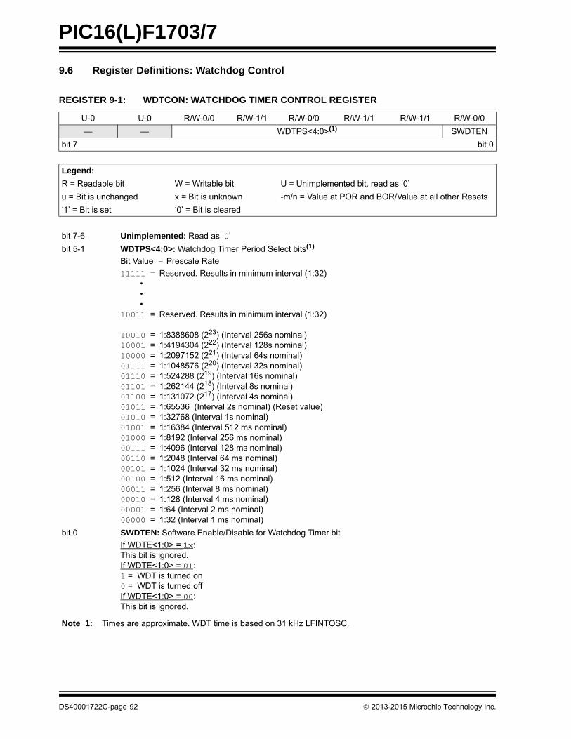
PIC16(L)F1703/7
9.6 Register Definitions: Watchdog Control
REGISTER 9-1: WDTCON: WATCHDOG TIMER CONTROL REGISTER
U-0 U-0 R/W-0/0 R/W-1/1 R/W-0/0 R/W-1/1 R/W-1/1 R/W-0/0
— — WDTPS<4:0>(1) SWDTEN
bit 7 bit 0
Legend:
R = Readable bit W = Writable bit U = Unimplemented bit, read as ‘0’
u = Bit is unchanged x = Bit is unknown -m/n = Value at POR and BOR/Value at all other Resets
‘1’ = Bit is set ‘0’ = Bit is cleared
bit 7-6 Unimplemented: Read as ‘0’
bit 5-1 WDTPS<4:0>: Watchdog Timer Period Select bits(1)
Bit Value = Prescale Rate
11111 = Reserved. Results in minimum interval (1:32) • • •
10011 = Reserved. Results in minimum interval (1:32)
10010 = 1:8388608 (223) (Interval 256s nominal)10001 = 1:4194304 (222) (Interval 128s nominal)10000 = 1:2097152 (221) (Interval 64s nominal)01111 = 1:1048576 (220) (Interval 32s nominal)01110 = 1:524288 (219) (Interval 16s nominal)01101 = 1:262144 (218) (Interval 8s nominal)01100 = 1:131072 (217) (Interval 4s nominal)01011 = 1:65536 (Interval 2s nominal) (Reset value)01010 = 1:32768 (Interval 1s nominal)01001 = 1:16384 (Interval 512 ms nominal)01000 = 1:8192 (Interval 256 ms nominal)00111 = 1:4096 (Interval 128 ms nominal)00110 = 1:2048 (Interval 64 ms nominal)00101 = 1:1024 (Interval 32 ms nominal)00100 = 1:512 (Interval 16 ms nominal)00011 = 1:256 (Interval 8 ms nominal)00010 = 1:128 (Interval 4 ms nominal)00001 = 1:64 (Interval 2 ms nominal)00000 = 1:32 (Interval 1 ms nominal)
bit 0 SWDTEN: Software Enable/Disable for Watchdog Timer bit
If WDTE<1:0> = 1x:This bit is ignored.If WDTE<1:0> = 01:1 = WDT is turned on0 = WDT is turned offIf WDTE<1:0> = 00:This bit is ignored.
Note 1: Times are approximate. WDT time is based on 31 kHz LFINTOSC.
DS40001722C-page 92 2013-2015 Microchip Technology Inc.
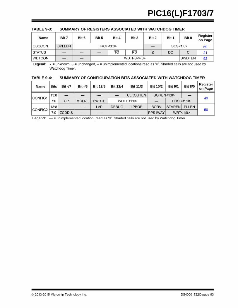
PIC16(L)F1703/7
TABLE 9-3: SUMMARY OF REGISTERS ASSOCIATED WITH WATCHDOG TIMER
TABLE 9-4: SUMMARY OF CONFIGURATION BITS ASSOCIATED WITH WATCHDOG TIMER
Name Bit 7 Bit 6 Bit 5 Bit 4 Bit 3 Bit 2 Bit 1 Bit 0Register on Page
OSCCON SPLLEN IRCF<3:0> — SCS<1:0> 69
STATUS — — — TO PD Z DC C 21
WDTCON — — WDTPS<4:0> SWDTEN 92
Legend: x = unknown, u = unchanged, – = unimplemented locations read as ‘0’. Shaded cells are not used by Watchdog Timer.
Name Bits Bit -/7 Bit -/6 Bit 13/5 Bit 12/4 Bit 11/3 Bit 10/2 Bit 9/1 Bit 8/0Register on Page
CONFIG113:8 — — — — CLKOUTEN BOREN<1:0> —
497:0 CP MCLRE PWRTE WDTE<1:0> — FOSC<1:0>
CONFIG213:8 — — LVP DEBUG LPBOR BORV STVREN PLLEN
507:0 ZCDDIS — — — — PPS1WAY WRT<1:0>
Legend: — = unimplemented location, read as ‘0’. Shaded cells are not used by Watchdog Timer.
2013-2015 Microchip Technology Inc. DS40001722C-page 93
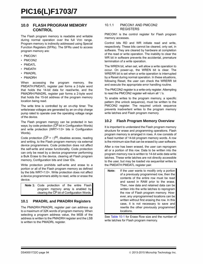
PIC16(L)F1703/7
10.0 FLASH PROGRAM MEMORY CONTROL
The Flash program memory is readable and writableduring normal operation over the full VDD range.Program memory is indirectly addressed using SpecialFunction Registers (SFRs). The SFRs used to accessprogram memory are:
• PMCON1
• PMCON2
• PMDATL
• PMDATH
• PMADRL
• PMADRH
When accessing the program memory, thePMDATH:PMDATL register pair forms a 2-byte wordthat holds the 14-bit data for read/write, and thePMADRH:PMADRL register pair forms a 2-byte wordthat holds the 15-bit address of the program memorylocation being read.
The write time is controlled by an on-chip timer. Thewrite/erase voltages are generated by an on-chip chargepump rated to operate over the operating voltage rangeof the device.
The Flash program memory can be protected in twoways; by code protection (CP bit in Configuration Words)and write protection (WRT<1:0> bits in ConfigurationWords).
Code protection (CP = 0)(1), disables access, readingand writing, to the Flash program memory via externaldevice programmers. Code protection does not affectthe self-write and erase functionality. Code protectioncan only be reset by a device programmer performinga Bulk Erase to the device, clearing all Flash programmemory, Configuration bits and User IDs.
Write protection prohibits self-write and erase to aportion or all of the Flash program memory as definedby the bits WRT<1:0>. Write protection does not affecta device programmers ability to read, write or erase thedevice.
10.1 PMADRL and PMADRH Registers
The PMADRH:PMADRL register pair can address upto a maximum of 32K words of program memory. Whenselecting a program address value, the MSB of theaddress is written to the PMADRH register and the LSBis written to the PMADRL register.
10.1.1 PMCON1 AND PMCON2 REGISTERS
PMCON1 is the control register for Flash programmemory accesses.
Control bits RD and WR initiate read and write,respectively. These bits cannot be cleared, only set, insoftware. They are cleared by hardware at completionof the read or write operation. The inability to clear theWR bit in software prevents the accidental, prematuretermination of a write operation.
The WREN bit, when set, will allow a write operation tooccur. On power-up, the WREN bit is clear. TheWRERR bit is set when a write operation is interruptedby a Reset during normal operation. In these situations,following Reset, the user can check the WRERR bitand execute the appropriate error handling routine.
The PMCON2 register is a write-only register. Attemptingto read the PMCON2 register will return all ‘0’s.
To enable writes to the program memory, a specificpattern (the unlock sequence), must be written to thePMCON2 register. The required unlock sequenceprevents inadvertent writes to the program memorywrite latches and Flash program memory.
10.2 Flash Program Memory Overview
It is important to understand the Flash program memorystructure for erase and programming operations. Flashprogram memory is arranged in rows. A row consists ofa fixed number of 14-bit program memory words. A rowis the minimum size that can be erased by user software.
After a row has been erased, the user can reprogramall or a portion of this row. Data to be written into theprogram memory row is written to 14-bit wide data writelatches. These write latches are not directly accessibleto the user, but may be loaded via sequential writes tothe PMDATH:PMDATL register pair.
See Table 10-1 for Erase Row size and the number ofwrite latches for Flash program memory.
Note 1: Code protection of the entire Flashprogram memory array is enabled byclearing the CP bit of Configuration Words.
Note: If the user wants to modify only a portionof a previously programmed row, then thecontents of the entire row must be readand saved in RAM prior to the erase.Then, new data and retained data can bewritten into the write latches to reprogramthe row of Flash program memory. How-ever, any unprogrammed locations can bewritten without first erasing the row. In thiscase, it is not necessary to save andrewrite the other previously programmedlocations.
DS40001722C-page 94 2013-2015 Microchip Technology Inc.

PIC16(L)F1703/7
10.2.1 READING THE FLASH PROGRAM MEMORY
To read a program memory location, the user must:
1. Write the desired address to thePMADRH:PMADRL register pair.
2. Clear the CFGS bit of the PMCON1 register.
3. Then, set control bit RD of the PMCON1 register.
Once the read control bit is set, the program memoryFlash controller will use the second instruction cycle toread the data. This causes the second instructionimmediately following the “BSF PMCON1,RD” instructionto be ignored. The data is available in the very next cycle,in the PMDATH:PMDATL register pair; therefore, it canbe read as two bytes in the following instructions.
PMDATH:PMDATL register pair will hold this value untilanother read or until it is written to by the user.
FIGURE 10-1: FLASH PROGRAM MEMORY READ FLOWCHART
TABLE 10-1: FLASH MEMORY ORGANIZATION BY DEVICE
DeviceRow Erase
(words)
Write Latches (words)
PIC16(L)F170316 16
PIC16(L)F1707
Note: The two instructions following a programmemory read are required to be NOPs.This prevents the user from executing a2-cycle instruction on the next instructionafter the RD bit is set.
Start Read Operation
Select Program or Configuration Memory
(CFGS)
Select Word Address
(PMADRH:PMADRL)
End Read Operation
Instruction Fetched ignoredNOP execution forced
Instruction Fetched ignoredNOP execution forced
Initiate Read operation(RD = 1)
Data read now in PMDATH:PMDATL
2013-2015 Microchip Technology Inc. DS40001722C-page 95
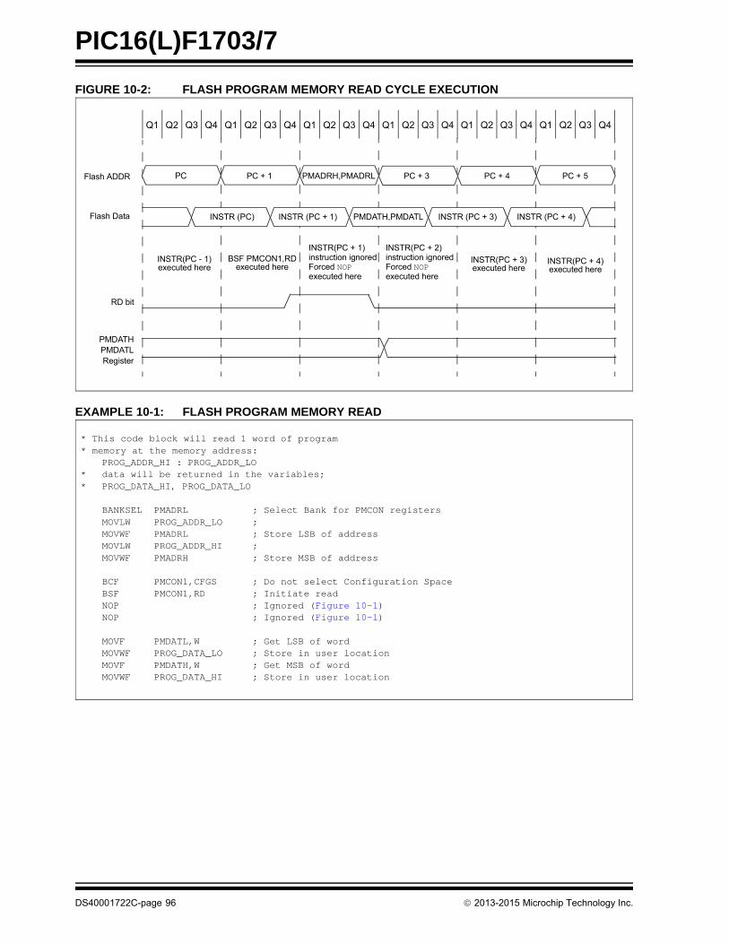
PIC16(L)F1703/7
FIGURE 10-2: FLASH PROGRAM MEMORY READ CYCLE EXECUTION
EXAMPLE 10-1: FLASH PROGRAM MEMORY READ
Q1 Q2 Q3 Q4 Q1 Q2 Q3 Q4 Q1 Q2 Q3 Q4 Q1 Q2 Q3 Q4 Q1 Q2 Q3 Q4 Q1 Q2 Q3 Q4
BSF PMCON1,RDexecuted here
INSTR(PC + 1)
executed here
PC PC + 1 PMADRH,PMADRL PC+3 PC + 5Flash ADDR
RD bit
PMDATH,PMDATL
PC + 3 PC + 4
INSTR (PC + 1)
INSTR(PC - 1)executed here
INSTR(PC + 3)executed here
INSTR(PC + 4)executed here
Flash Data
PMDATHPMDATLRegister
INSTR (PC) INSTR (PC + 3) INSTR (PC + 4)
instruction ignoredForced NOP
INSTR(PC + 2)
executed here
instruction ignoredForced NOP
* This code block will read 1 word of program* memory at the memory address:
PROG_ADDR_HI : PROG_ADDR_LO* data will be returned in the variables;* PROG_DATA_HI, PROG_DATA_LO
BANKSEL PMADRL ; Select Bank for PMCON registersMOVLW PROG_ADDR_LO ; MOVWF PMADRL ; Store LSB of addressMOVLW PROG_ADDR_HI ; MOVWF PMADRH ; Store MSB of address
BCF PMCON1,CFGS ; Do not select Configuration SpaceBSF PMCON1,RD ; Initiate readNOP ; Ignored (Figure 10-1)NOP ; Ignored (Figure 10-1)
MOVF PMDATL,W ; Get LSB of wordMOVWF PROG_DATA_LO ; Store in user locationMOVF PMDATH,W ; Get MSB of wordMOVWF PROG_DATA_HI ; Store in user location
DS40001722C-page 96 2013-2015 Microchip Technology Inc.
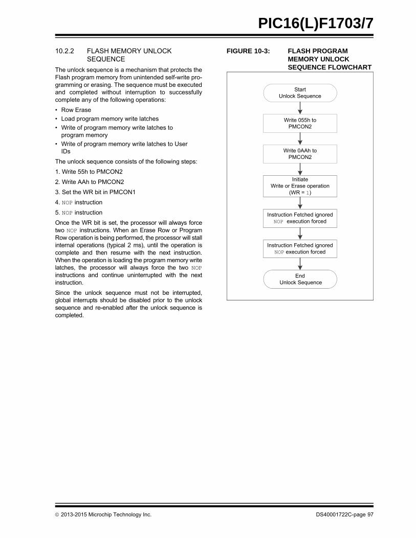
PIC16(L)F1703/7
10.2.2 FLASH MEMORY UNLOCK SEQUENCE
The unlock sequence is a mechanism that protects theFlash program memory from unintended self-write pro-gramming or erasing. The sequence must be executedand completed without interruption to successfullycomplete any of the following operations:
• Row Erase
• Load program memory write latches
• Write of program memory write latches to program memory
• Write of program memory write latches to User IDs
The unlock sequence consists of the following steps:
1. Write 55h to PMCON2
2. Write AAh to PMCON2
3. Set the WR bit in PMCON1
4. NOP instruction
5. NOP instruction
Once the WR bit is set, the processor will always forcetwo NOP instructions. When an Erase Row or ProgramRow operation is being performed, the processor will stallinternal operations (typical 2 ms), until the operation iscomplete and then resume with the next instruction.When the operation is loading the program memory writelatches, the processor will always force the two NOPinstructions and continue uninterrupted with the nextinstruction.
Since the unlock sequence must not be interrupted,global interrupts should be disabled prior to the unlocksequence and re-enabled after the unlock sequence iscompleted.
FIGURE 10-3: FLASH PROGRAM MEMORY UNLOCK SEQUENCE FLOWCHART
Write 055h to PMCON2
Start Unlock Sequence
Write 0AAh toPMCON2
InitiateWrite or Erase operation
(WR = 1)
Instruction Fetched ignoredNOP execution forced
End Unlock Sequence
Instruction Fetched ignoredNOP execution forced
2013-2015 Microchip Technology Inc. DS40001722C-page 97
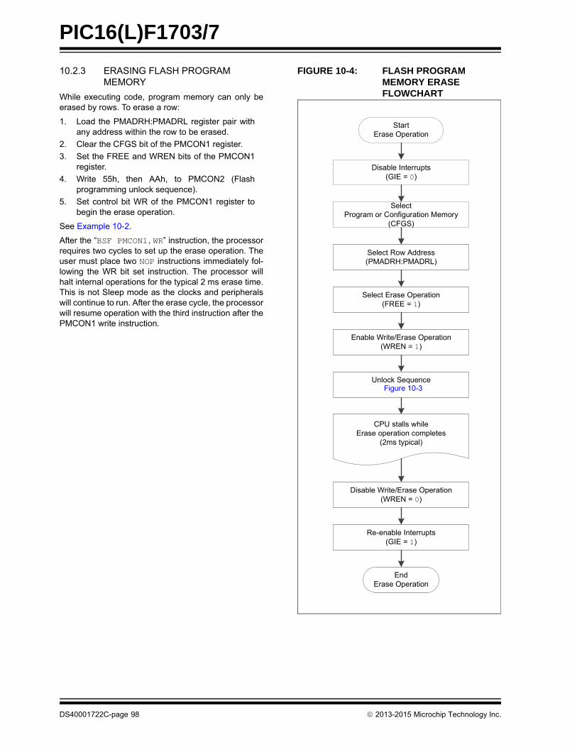
PIC16(L)F1703/7
10.2.3 ERASING FLASH PROGRAM MEMORY
While executing code, program memory can only beerased by rows. To erase a row:
1. Load the PMADRH:PMADRL register pair withany address within the row to be erased.
2. Clear the CFGS bit of the PMCON1 register.
3. Set the FREE and WREN bits of the PMCON1register.
4. Write 55h, then AAh, to PMCON2 (Flashprogramming unlock sequence).
5. Set control bit WR of the PMCON1 register tobegin the erase operation.
See Example 10-2.
After the “BSF PMCON1,WR” instruction, the processorrequires two cycles to set up the erase operation. Theuser must place two NOP instructions immediately fol-lowing the WR bit set instruction. The processor willhalt internal operations for the typical 2 ms erase time.This is not Sleep mode as the clocks and peripheralswill continue to run. After the erase cycle, the processorwill resume operation with the third instruction after thePMCON1 write instruction.
FIGURE 10-4: FLASH PROGRAM MEMORY ERASE FLOWCHART
Disable Interrupts(GIE = 0)
Start Erase Operation
Select Program or Configuration Memory
(CFGS)
Select Row Address(PMADRH:PMADRL)
Select Erase Operation(FREE = 1)
Enable Write/Erase Operation (WREN = 1)
Unlock Sequence(FIGURE x-x)
Disable Write/Erase Operation (WREN = 0)
Re-enable Interrupts(GIE = 1)
End Erase Operation
CPU stalls while Erase operation completes
(2ms typical)
Figure 10-3
DS40001722C-page 98 2013-2015 Microchip Technology Inc.

PIC16(L)F1703/7
EXAMPLE 10-2: ERASING ONE ROW OF PROGRAM MEMORY
; This row erase routine assumes the following:; 1. A valid address within the erase row is loaded in ADDRH:ADDRL; 2. ADDRH and ADDRL are located in shared data memory 0x70 - 0x7F (common RAM)
BCF INTCON,GIE ; Disable ints so required sequences will execute properlyBANKSEL PMADRLMOVF ADDRL,W ; Load lower 8 bits of erase address boundaryMOVWF PMADRLMOVF ADDRH,W ; Load upper 6 bits of erase address boundaryMOVWF PMADRHBCF PMCON1,CFGS ; Not configuration spaceBSF PMCON1,FREE ; Specify an erase operationBSF PMCON1,WREN ; Enable writes
MOVLW 55h ; Start of required sequence to initiate eraseMOVWF PMCON2 ; Write 55hMOVLW 0AAh ;MOVWF PMCON2 ; Write AAhBSF PMCON1,WR ; Set WR bit to begin eraseNOP ; NOP instructions are forced as processor startsNOP ; row erase of program memory.
;; The processor stalls until the erase process is complete; after erase processor continues with 3rd instruction
BCF PMCON1,WREN ; Disable writesBSF INTCON,GIE ; Enable interrupts
Re
qu
ire
dS
eq
ue
nce
2013-2015 Microchip Technology Inc. DS40001722C-page 99

PIC16(L)F1703/7
10.2.4 WRITING TO FLASH PROGRAM MEMORY
Program memory is programmed using the followingsteps:
1. Load the address in PMADRH:PMADRL of therow to be programmed.
2. Load each write latch with data.
3. Initiate a programming operation.
4. Repeat steps 1 through 3 until all data is written.
Before writing to program memory, the word(s) to bewritten must be erased or previously unwritten.Program memory can only be erased one row at a time.No automatic erase occurs upon the initiation of thewrite.
Program memory can be written one or more words ata time. The maximum number of words written at onetime is equal to the number of write latches. SeeFigure 10-5 (row writes to program memory with 16write latches) for more details.
The write latches are aligned to the Flash row addressboundary defined by the upper 10-bits ofPMADRH:PMADRL, (PMADRH<6:0>:PMADRL<7:5>)with the lower five bits of PMADRL, (PMADRL<4:0>)determining the write latch being loaded. Write opera-tions do not cross these boundaries. At the completionof a program memory write operation, the data in thewrite latches is reset to contain 0x3FFF.
The following steps should be completed to load thewrite latches and program a row of program memory.These steps are divided into two parts. First, each writelatch is loaded with data from the PMDATH:PMDATLusing the unlock sequence with LWLO = 1. When thelast word to be loaded into the write latch is ready, theLWLO bit is cleared and the unlock sequenceexecuted. This initiates the programming operation,writing all the latches into Flash program memory.
1. Set the WREN bit of the PMCON1 register.
2. Clear the CFGS bit of the PMCON1 register.
3. Set the LWLO bit of the PMCON1 register.When the LWLO bit of the PMCON1 register is‘1’, the write sequence will only load the writelatches and will not initiate the write to Flashprogram memory.
4. Load the PMADRH:PMADRL register pair withthe address of the location to be written.
5. Load the PMDATH:PMDATL register pair withthe program memory data to be written.
6. Execute the unlock sequence (Section 10.2.2“Flash Memory Unlock Sequence”). The writelatch is now loaded.
7. Increment the PMADRH:PMADRL register pairto point to the next location.
8. Repeat steps 5 through 7 until all but the lastwrite latch has been loaded.
9. Clear the LWLO bit of the PMCON1 register.When the LWLO bit of the PMCON1 register is‘0’, the write sequence will initiate the write toFlash program memory.
10. Load the PMDATH:PMDATL register pair withthe program memory data to be written.
11. Execute the unlock sequence (Section 10.2.2“Flash Memory Unlock Sequence”). Theentire program memory latch content is nowwritten to Flash program memory.
An example of the complete write sequence is shown inExample 10-3. The initial address is loaded into thePMADRH:PMADRL register pair; the data is loadedusing indirect addressing.
Note: The special unlock sequence is requiredto load a write latch with data or initiate aFlash programming operation. If theunlock sequence is interrupted, writing tothe latches or program memory will not beinitiated.
Note: The program memory write latches arereset to the blank state (0x3FFF) at thecompletion of every write or eraseoperation. As a result, it is not necessaryto load all the program memory writelatches. Unloaded latches will remain inthe blank state.
DS40001722C-page 100 2013-2015 Microchip Technology Inc.
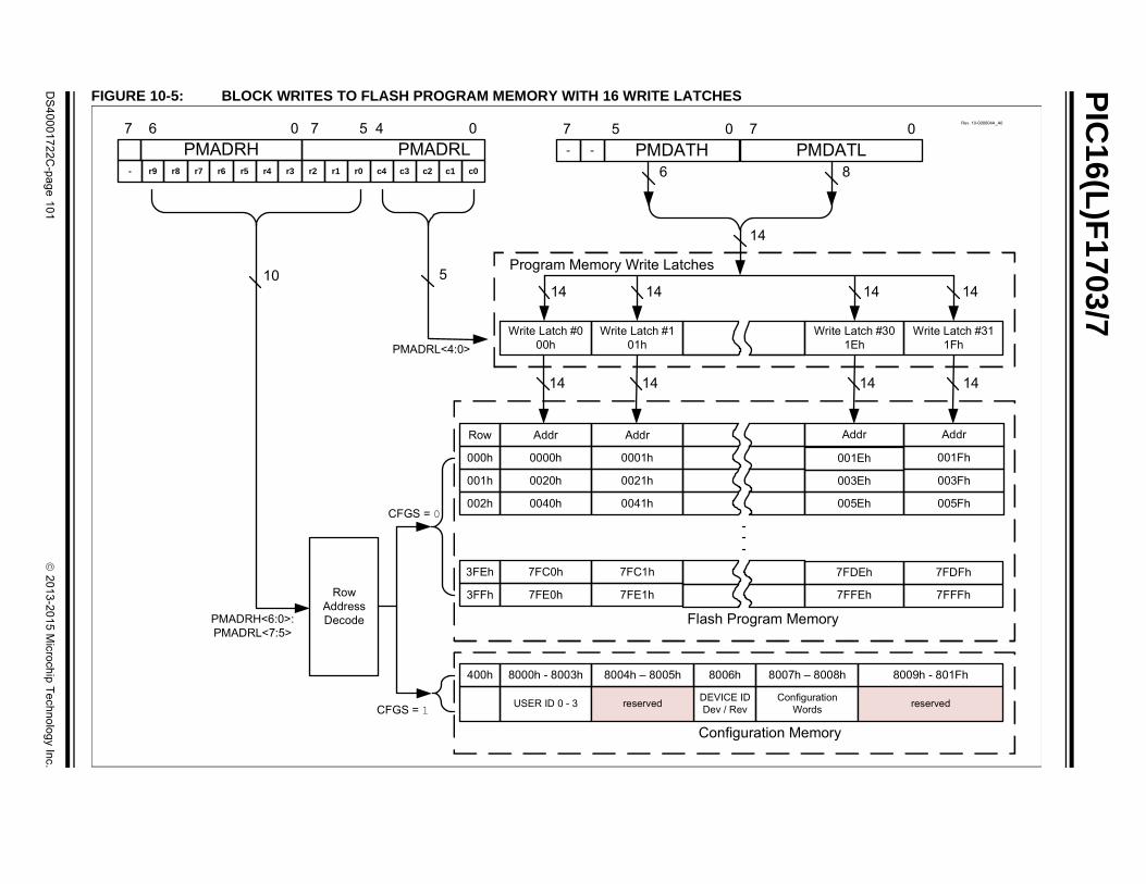
PIC
16(L)F
1703/7
DS
40
00
17
22
C-p
ag
e 1
01
2
01
3-2
01
5 M
icroch
ip T
ech
no
log
y Inc.
8
Write Latch #311Fh
1414
14
Memory
Write Latch #301Eh
Addr Addr
001Fh001Eh
003Fh003Eh
005Fh005Eh
7FDFh7FDEh
7FFFh7FFEh
14
8009h - 801Fh
onfigurationWords
7h – 8008h
reserved
Memory
PMDATL 0
Rev. 10-000004A_A0
FIGURE 10-5: BLOCK WRITES TO FLASH PROGRAM MEMORY WITH 16 WRITE LATCHES
6
14
1414
Program Memory Write Latches
14 14
PMADRH<6:0>:PMADRL<7:5>
Flash Program
Row
Row Address Decode
Addr
Write Latch #101h
Write Latch #000h
Addr
000h 0000h 0001h
001h 0020h 0021h
002h 0040h 0041h
3FEh 7FC0h 7FC1h
3FFh 7FE0h 7FE1h
PMADRL<4:0>
400h 8000h - 8003h
CUSER ID 0 - 3
8008006h
DEVICE IDDev / Rev
reserved
Configuration
CFGS = 0
CFGS = 1
PMADRH PMADRL7 6 0 7 5 4 0
c4 c3 c2 c1 c0r9 r8 r7 r6 r5 r4 r3- r1 r0r2
510
PMDATH7 5 0 7
--
8004h – 8005h

PIC16(L)F1703/7
FIGURE 10-6: FLASH PROGRAM MEMORY WRITE FLOWCHART
Disable Interrupts(GIE = 0)
Start Write Operation
Select Program or Config. Memory
(CFGS)
Select Row Address(PMADRH:PMADRL)
Select Write Operation(FREE = 0)
Enable Write/Erase Operation (WREN = 1)
Unlock Sequence(Figure x-x)
Disable Write/Erase Operation
(WREN = 0)
Re-enable Interrupts(GIE = 1)
End Write Operation
No delay when writing to Program Memory Latches
Determine number of words to be written into Program or
Configuration Memory. The number of words cannot exceed the number of words
per row.(word_cnt) Load the value to write
(PMDATH:PMDATL)
Update the word counter (word_cnt--)
Last word to write ?
Increment Address(PMADRH:PMADRL++)
Unlock Sequence(Figure x-x)
CPU stalls while Write operation completes
(2ms typical)
Load Write Latches Only(LWLO = 1)
Write Latches to Flash(LWLO = 0)
No
Yes Figure 10-3
Figure 10-3
DS40001722C-page 102 2013-2015 Microchip Technology Inc.
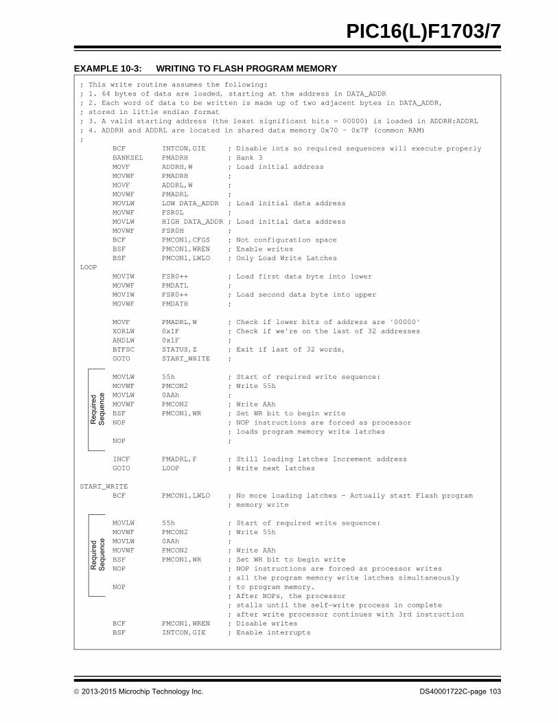
PIC16(L)F1703/7
EXAMPLE 10-3: WRITING TO FLASH PROGRAM MEMORY
; This write routine assumes the following:; 1. 64 bytes of data are loaded, starting at the address in DATA_ADDR; 2. Each word of data to be written is made up of two adjacent bytes in DATA_ADDR,; stored in little endian format; 3. A valid starting address (the least significant bits = 00000) is loaded in ADDRH:ADDRL; 4. ADDRH and ADDRL are located in shared data memory 0x70 - 0x7F (common RAM);
BCF INTCON,GIE ; Disable ints so required sequences will execute properlyBANKSEL PMADRH ; Bank 3MOVF ADDRH,W ; Load initial addressMOVWF PMADRH ;MOVF ADDRL,W ;MOVWF PMADRL ;MOVLW LOW DATA_ADDR ; Load initial data addressMOVWF FSR0L ;MOVLW HIGH DATA_ADDR ; Load initial data addressMOVWF FSR0H ;BCF PMCON1,CFGS ; Not configuration spaceBSF PMCON1,WREN ; Enable writesBSF PMCON1,LWLO ; Only Load Write Latches
LOOPMOVIW FSR0++ ; Load first data byte into lowerMOVWF PMDATL ;MOVIW FSR0++ ; Load second data byte into upperMOVWF PMDATH ;
MOVF PMADRL,W ; Check if lower bits of address are '00000'XORLW 0x1F ; Check if we're on the last of 32 addressesANDLW 0x1F ;BTFSC STATUS,Z ; Exit if last of 32 words,GOTO START_WRITE ;
MOVLW 55h ; Start of required write sequence:MOVWF PMCON2 ; Write 55hMOVLW 0AAh ;MOVWF PMCON2 ; Write AAhBSF PMCON1,WR ; Set WR bit to begin writeNOP ; NOP instructions are forced as processor
; loads program memory write latchesNOP ;
INCF PMADRL,F ; Still loading latches Increment addressGOTO LOOP ; Write next latches
START_WRITEBCF PMCON1,LWLO ; No more loading latches - Actually start Flash program
; memory write
MOVLW 55h ; Start of required write sequence:MOVWF PMCON2 ; Write 55hMOVLW 0AAh ;MOVWF PMCON2 ; Write AAhBSF PMCON1,WR ; Set WR bit to begin writeNOP ; NOP instructions are forced as processor writes
; all the program memory write latches simultaneouslyNOP ; to program memory.
; After NOPs, the processor; stalls until the self-write process in complete; after write processor continues with 3rd instruction
BCF PMCON1,WREN ; Disable writesBSF INTCON,GIE ; Enable interrupts
Re
qu
ire
dS
eq
ue
nce
Re
qu
ire
dS
eq
ue
nce
2013-2015 Microchip Technology Inc. DS40001722C-page 103
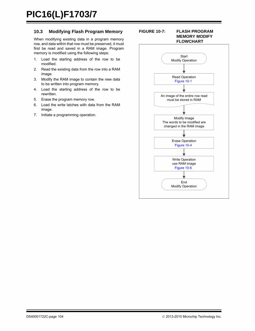
PIC16(L)F1703/7
DS
10.3 Modifying Flash Program Memory
When modifying existing data in a program memoryrow, and data within that row must be preserved, it mustfirst be read and saved in a RAM image. Programmemory is modified using the following steps:
1. Load the starting address of the row to bemodified.
2. Read the existing data from the row into a RAMimage.
3. Modify the RAM image to contain the new datato be written into program memory.
4. Load the starting address of the row to berewritten.
5. Erase the program memory row.
6. Load the write latches with data from the RAMimage.
7. Initiate a programming operation.
FIGURE 10-7: FLASH PROGRAM MEMORY MODIFY FLOWCHART
Start Modify Operation
Read Operation(Figure x.x)
Erase Operation(Figure x.x)
Modify ImageThe words to be modified are changed in the RAM image
End Modify Operation
Write Operationuse RAM image
(Figure x.x)
An image of the entire row read must be stored in RAM
Figure 10-1
Figure 10-4
Figure 10-6
40001722C-page 104 2013-2015 Microchip Technology Inc.
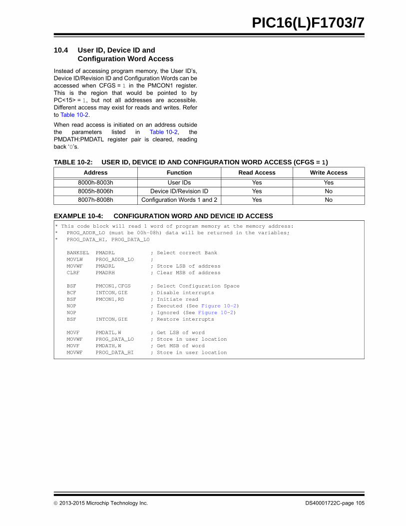
PIC16(L)F1703/7
10.4 User ID, Device ID and Configuration Word Access
Instead of accessing program memory, the User ID’s,Device ID/Revision ID and Configuration Words can beaccessed when CFGS = 1 in the PMCON1 register.This is the region that would be pointed to byPC<15> = 1, but not all addresses are accessible.Different access may exist for reads and writes. Referto Table 10-2.
When read access is initiated on an address outsidethe parameters listed in Table 10-2, thePMDATH:PMDATL register pair is cleared, readingback ‘0’s.
TABLE 10-2: USER ID, DEVICE ID AND CONFIGURATION WORD ACCESS (CFGS = 1)
EXAMPLE 10-4: CONFIGURATION WORD AND DEVICE ID ACCESS
Address Function Read Access Write Access
8000h-8003h User IDs Yes Yes
8005h-8006h Device ID/Revision ID Yes No
8007h-8008h Configuration Words 1 and 2 Yes No
* This code block will read 1 word of program memory at the memory address:* PROG_ADDR_LO (must be 00h-08h) data will be returned in the variables;* PROG_DATA_HI, PROG_DATA_LO
BANKSEL PMADRL ; Select correct BankMOVLW PROG_ADDR_LO ; MOVWF PMADRL ; Store LSB of addressCLRF PMADRH ; Clear MSB of address
BSF PMCON1,CFGS ; Select Configuration Space BCF INTCON,GIE ; Disable interruptsBSF PMCON1,RD ; Initiate readNOP ; Executed (See Figure 10-2)NOP ; Ignored (See Figure 10-2)BSF INTCON,GIE ; Restore interrupts
MOVF PMDATL,W ; Get LSB of wordMOVWF PROG_DATA_LO ; Store in user locationMOVF PMDATH,W ; Get MSB of wordMOVWF PROG_DATA_HI ; Store in user location
2013-2015 Microchip Technology Inc. DS40001722C-page 105
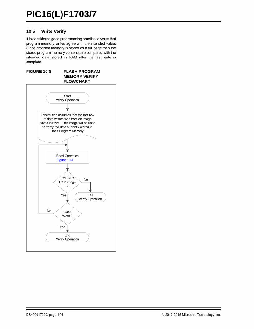
PIC16(L)F1703/7
10.5 Write Verify
It is considered good programming practice to verify thatprogram memory writes agree with the intended value.Since program memory is stored as a full page then thestored program memory contents are compared with theintended data stored in RAM after the last write iscomplete.
FIGURE 10-8: FLASH PROGRAM MEMORY VERIFY FLOWCHART
Start Verify Operation
Read Operation(Figure x.x)
End Verify Operation
This routine assumes that the last row of data written was from an image
saved in RAM. This image will be used to verify the data currently stored in
Flash Program Memory.
PMDAT = RAM image
?
LastWord ?
Fail Verify Operation
No
Yes
Yes
No
Figure 10-1
DS40001722C-page 106 2013-2015 Microchip Technology Inc.
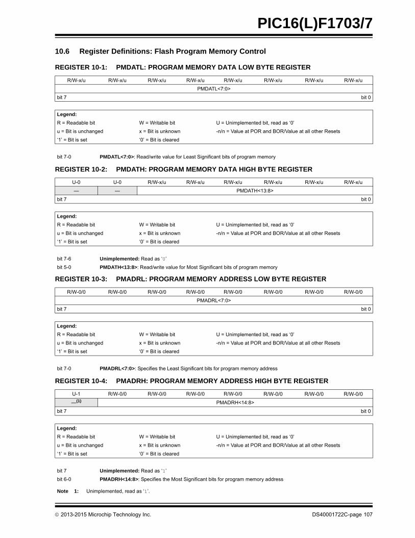
PIC16(L)F1703/7
10.6 Register Definitions: Flash Program Memory Control
REGISTER 10-1: PMDATL: PROGRAM MEMORY DATA LOW BYTE REGISTER
R/W-x/u R/W-x/u R/W-x/u R/W-x/u R/W-x/u R/W-x/u R/W-x/u R/W-x/u
PMDATL<7:0>
bit 7 bit 0
Legend:
R = Readable bit W = Writable bit U = Unimplemented bit, read as ‘0’
u = Bit is unchanged x = Bit is unknown -n/n = Value at POR and BOR/Value at all other Resets
‘1’ = Bit is set ‘0’ = Bit is cleared
bit 7-0 PMDATL<7:0>: Read/write value for Least Significant bits of program memory
REGISTER 10-2: PMDATH: PROGRAM MEMORY DATA HIGH BYTE REGISTER
U-0 U-0 R/W-x/u R/W-x/u R/W-x/u R/W-x/u R/W-x/u R/W-x/u
— — PMDATH<13:8>
bit 7 bit 0
Legend:
R = Readable bit W = Writable bit U = Unimplemented bit, read as ‘0’
u = Bit is unchanged x = Bit is unknown -n/n = Value at POR and BOR/Value at all other Resets
‘1’ = Bit is set ‘0’ = Bit is cleared
bit 7-6 Unimplemented: Read as ‘0’
bit 5-0 PMDATH<13:8>: Read/write value for Most Significant bits of program memory
REGISTER 10-3: PMADRL: PROGRAM MEMORY ADDRESS LOW BYTE REGISTER
R/W-0/0 R/W-0/0 R/W-0/0 R/W-0/0 R/W-0/0 R/W-0/0 R/W-0/0 R/W-0/0
PMADRL<7:0>
bit 7 bit 0
Legend:
R = Readable bit W = Writable bit U = Unimplemented bit, read as ‘0’
u = Bit is unchanged x = Bit is unknown -n/n = Value at POR and BOR/Value at all other Resets
‘1’ = Bit is set ‘0’ = Bit is cleared
bit 7-0 PMADRL<7:0>: Specifies the Least Significant bits for program memory address
REGISTER 10-4: PMADRH: PROGRAM MEMORY ADDRESS HIGH BYTE REGISTER
U-1 R/W-0/0 R/W-0/0 R/W-0/0 R/W-0/0 R/W-0/0 R/W-0/0 R/W-0/0
—(1) PMADRH<14:8>
bit 7 bit 0
Legend:
R = Readable bit W = Writable bit U = Unimplemented bit, read as ‘0’
u = Bit is unchanged x = Bit is unknown -n/n = Value at POR and BOR/Value at all other Resets
‘1’ = Bit is set ‘0’ = Bit is cleared
bit 7 Unimplemented: Read as ‘1’
bit 6-0 PMADRH<14:8>: Specifies the Most Significant bits for program memory address
Note 1: Unimplemented, read as ‘1’.
2013-2015 Microchip Technology Inc. DS40001722C-page 107
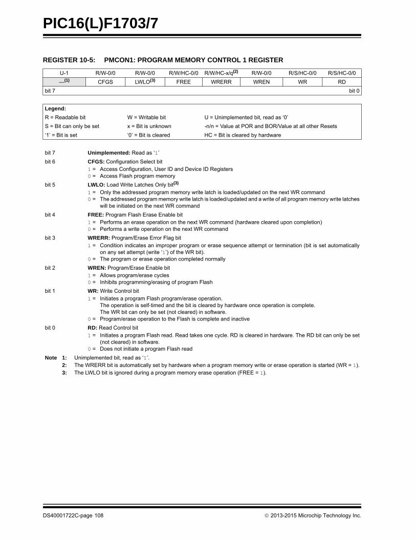
PIC16(L)F1703/7
REGISTER 10-5: PMCON1: PROGRAM MEMORY CONTROL 1 REGISTER
U-1 R/W-0/0 R/W-0/0 R/W/HC-0/0 R/W/HC-x/q(2) R/W-0/0 R/S/HC-0/0 R/S/HC-0/0
—(1) CFGS LWLO(3) FREE WRERR WREN WR RD
bit 7 bit 0
Legend:
R = Readable bit W = Writable bit U = Unimplemented bit, read as ‘0’
S = Bit can only be set x = Bit is unknown -n/n = Value at POR and BOR/Value at all other Resets
‘1’ = Bit is set ‘0’ = Bit is cleared HC = Bit is cleared by hardware
bit 7 Unimplemented: Read as ‘1’
bit 6 CFGS: Configuration Select bit1 = Access Configuration, User ID and Device ID Registers0 = Access Flash program memory
bit 5 LWLO: Load Write Latches Only bit(3)
1 = Only the addressed program memory write latch is loaded/updated on the next WR command0 = The addressed program memory write latch is loaded/updated and a write of all program memory write latches
will be initiated on the next WR command
bit 4 FREE: Program Flash Erase Enable bit 1 = Performs an erase operation on the next WR command (hardware cleared upon completion)0 = Performs a write operation on the next WR command
bit 3 WRERR: Program/Erase Error Flag bit1 = Condition indicates an improper program or erase sequence attempt or termination (bit is set automatically
on any set attempt (write ‘1’) of the WR bit).0 = The program or erase operation completed normally
bit 2 WREN: Program/Erase Enable bit1 = Allows program/erase cycles0 = Inhibits programming/erasing of program Flash
bit 1 WR: Write Control bit1 = Initiates a program Flash program/erase operation.
The operation is self-timed and the bit is cleared by hardware once operation is complete. The WR bit can only be set (not cleared) in software.
0 = Program/erase operation to the Flash is complete and inactive
bit 0 RD: Read Control bit1 = Initiates a program Flash read. Read takes one cycle. RD is cleared in hardware. The RD bit can only be set
(not cleared) in software.0 = Does not initiate a program Flash read
Note 1: Unimplemented bit, read as ‘1’.2: The WRERR bit is automatically set by hardware when a program memory write or erase operation is started (WR = 1).3: The LWLO bit is ignored during a program memory erase operation (FREE = 1).
DS40001722C-page 108 2013-2015 Microchip Technology Inc.
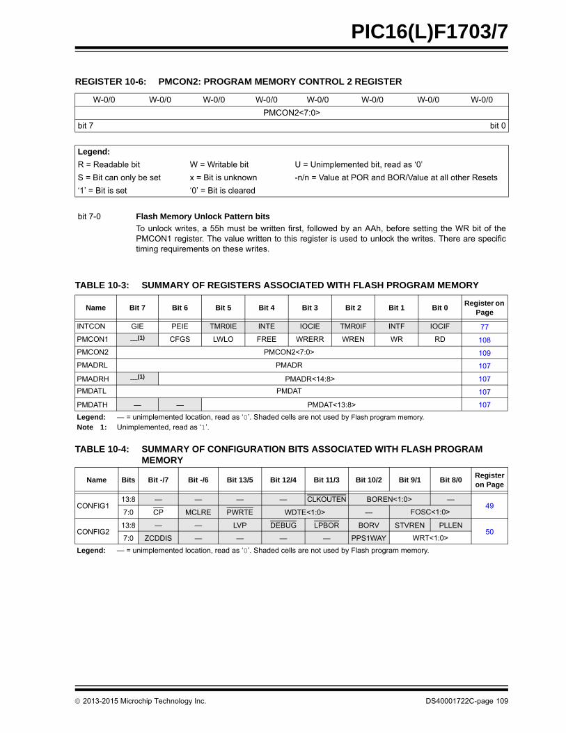
PIC16(L)F1703/7
TABLE 10-3: SUMMARY OF REGISTERS ASSOCIATED WITH FLASH PROGRAM MEMORY
TABLE 10-4: SUMMARY OF CONFIGURATION BITS ASSOCIATED WITH FLASH PROGRAM MEMORY
REGISTER 10-6: PMCON2: PROGRAM MEMORY CONTROL 2 REGISTER
W-0/0 W-0/0 W-0/0 W-0/0 W-0/0 W-0/0 W-0/0 W-0/0
PMCON2<7:0>
bit 7 bit 0
Legend:
R = Readable bit W = Writable bit U = Unimplemented bit, read as ‘0’
S = Bit can only be set x = Bit is unknown -n/n = Value at POR and BOR/Value at all other Resets
‘1’ = Bit is set ‘0’ = Bit is cleared
bit 7-0 Flash Memory Unlock Pattern bits
To unlock writes, a 55h must be written first, followed by an AAh, before setting the WR bit of thePMCON1 register. The value written to this register is used to unlock the writes. There are specifictiming requirements on these writes.
Name Bit 7 Bit 6 Bit 5 Bit 4 Bit 3 Bit 2 Bit 1 Bit 0Register on
Page
INTCON GIE PEIE TMR0IE INTE IOCIE TMR0IF INTF IOCIF 77
PMCON1 —(1) CFGS LWLO FREE WRERR WREN WR RD 108
PMCON2 PMCON2<7:0> 109
PMADRL PMADR 107
PMADRH —(1) PMADR<14:8> 107
PMDATL PMDAT 107
PMDATH — — PMDAT<13:8> 107
Legend: — = unimplemented location, read as ‘0’. Shaded cells are not used by Flash program memory.Note 1: Unimplemented, read as ‘1’.
Name Bits Bit -/7 Bit -/6 Bit 13/5 Bit 12/4 Bit 11/3 Bit 10/2 Bit 9/1 Bit 8/0Register on Page
CONFIG113:8 — — — — CLKOUTEN BOREN<1:0> —
497:0 CP MCLRE PWRTE WDTE<1:0> — FOSC<1:0>
CONFIG213:8 — — LVP DEBUG LPBOR BORV STVREN PLLEN
507:0 ZCDDIS — — — — PPS1WAY WRT<1:0>
Legend: — = unimplemented location, read as ‘0’. Shaded cells are not used by Flash program memory.
2013-2015 Microchip Technology Inc. DS40001722C-page 109
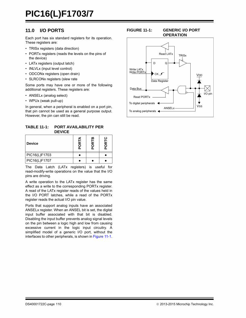
PIC16(L)F1703/7
11.0 I/O PORTS
Each port has six standard registers for its operation.These registers are:
• TRISx registers (data direction)
• PORTx registers (reads the levels on the pins of the device)
• LATx registers (output latch)
• INLVLx (input level control)
• ODCONx registers (open drain)
• SLRCONx registers (slew rate
Some ports may have one or more of the followingadditional registers. These registers are:
• ANSELx (analog select)
• WPUx (weak pull-up)
In general, when a peripheral is enabled on a port pin,that pin cannot be used as a general purpose output.However, the pin can still be read.
The Data Latch (LATx registers) is useful forread-modify-write operations on the value that the I/Opins are driving.
A write operation to the LATx register has the sameeffect as a write to the corresponding PORTx register.A read of the LATx register reads of the values held inthe I/O PORT latches, while a read of the PORTxregister reads the actual I/O pin value.
Ports that support analog inputs have an associatedANSELx register. When an ANSEL bit is set, the digitalinput buffer associated with that bit is disabled.Disabling the input buffer prevents analog signal levelson the pin between a logic high and low from causingexcessive current in the logic input circuitry. Asimplified model of a generic I/O port, without theinterfaces to other peripherals, is shown in Figure 11-1.
FIGURE 11-1: GENERIC I/O PORT OPERATION
TABLE 11-1: PORT AVAILABILITY PER DEVICE
Device
PO
RTA
PO
RT
B
PO
RT
C
PIC16(L)F1703 ● ●
PIC16(L)F1707 ● ● ●
QD
CK
Write LATx
Data Register
I/O pinRead PORTx
Write PORTx
TRISxRead LATx
Data Bus
To digital peripherals
ANSELx
VDD
VSS
To analog peripherals
DS40001722C-page 110 2013-2015 Microchip Technology Inc.
PIC16(L)F1703/7
11.1 PORTA Registers
11.1.1 DATA REGISTER
PORTA is a 6-bit wide, bidirectional port. Thecorresponding data direction register is TRISA(Register 11-2). Setting a TRISA bit (= 1) will make thecorresponding PORTA pin an input (i.e., disable theoutput driver). Clearing a TRISA bit (= 0) will make thecorresponding PORTA pin an output (i.e., enablesoutput driver and puts the contents of the output latchon the selected pin). The exception is RA3, which isinput-only and its TRIS bit will always read as ‘1’.Example 11-1 shows how to initialize PORTA.
Reading the PORTA register (Register 11-1) reads thestatus of the pins, whereas writing to it will write to thePORT latch. All write operations are read-modify-writeoperations. Therefore, a write to a port implies that theport pins are read, this value is modified and thenwritten to the PORT data latch (LATA).
11.1.2 DIRECTION CONTROL
The TRISA register (Register 11-2) controls thePORTA pin output drivers, even when they are beingused as analog inputs. The user should ensure the bitsin the TRISA register are maintained set when usingthem as analog inputs. I/O pins configured as analoginputs always read ‘0’.
11.1.3 OPEN DRAIN CONTROL
The ODCONA register (Register 11-6) controls theopen-drain feature of the port. Open drain operation isindependently selected for each pin. When anODCONA bit is set, the corresponding port outputbecomes an open drain driver capable of sinkingcurrent only. When an ODCONA bit is cleared, thecorresponding port output pin is the standard push-pulldrive capable of sourcing and sinking current.
11.1.4 SLEW RATE CONTROL
The SLRCONA register (Register 11-7) controls theslew rate option for each port pin. Slew rate control isindependently selectable for each port pin. When anSLRCONA bit is set, the corresponding port pin drive isslew rate limited. When an SLRCONA bit is cleared,The corresponding port pin drive slews at the maximumrate possible.
11.1.5 INPUT THRESHOLD CONTROL
The INLVLA register (Register 11-8) controls the inputvoltage threshold for each of the available PORTA inputpins. A selection between the Schmitt Trigger CMOS orthe TTL Compatible thresholds is available. The inputthreshold is important in determining the value of a readof the PORTA register and also the level at which aninterrupt-on-change occurs, if that feature is enabled.See Table 26-4 for more information on thresholdlevels.
11.1.6 ANALOG CONTROL
The ANSELA register (Register 11-4) is used toconfigure the Input mode of an I/O pin to analog.Setting the appropriate ANSELA bit high will cause alldigital reads on the pin to be read as ‘0’ and allowanalog functions on the pin to operate correctly.
The state of the ANSELA bits has no effect on digitaloutput functions. A pin with TRIS clear and ANSEL setwill still operate as a digital output, but the Input modewill be analog. This can cause unexpected behaviorwhen executing read-modify-write instructions on theaffected port.
EXAMPLE 11-1: INITIALIZING PORTA
Note: Changing the input threshold selectionshould be performed while all peripheralmodules are disabled. Changing thethreshold level during the time a module isactive may inadvertently generate atransition associated with an input pin,regardless of the actual voltage level onthat pin.
Note: The ANSELA bits default to the Analogmode after Reset. To use any pins asdigital general purpose or peripheralinputs, the corresponding ANSEL bitsmust be initialized to ‘0’ by user software.
; This code example illustrates; initializing the PORTA register. The ; other ports are initialized in the same; manner.
BANKSEL PORTA ;CLRF PORTA ;Init PORTABANKSEL LATA ;Data LatchCLRF LATA ;BANKSEL ANSELA ;CLRF ANSELA ;digital I/OBANKSEL TRISA ;MOVLW B'00111000' ;Set RA<5:3> as inputsMOVWF TRISA ;and set RA<2:0> as
;outputs
2013-2015 Microchip Technology Inc. DS40001722C-page 111
PIC16(L)F1703/7
11.1.7 PORTA FUNCTIONS AND OUTPUT PRIORITIES
Each PORTA pin is multiplexed with other functions.
Each pin defaults to the PORT latch data after reset.Other functions are selected with the peripheral pinselect logic. See Section 12.0 “Peripheral Pin Select(PPS) Module” for more information.
Analog input functions, such as ADC inputs, are notshown in the peripheral pin select lists. These inputsare active when the I/O pin is set for Analog mode usingthe ANSELA register. Digital output functions maycontinue to control the pin when it is in Analog mode.
DS40001722C-page 112 2013-2015 Microchip Technology Inc.
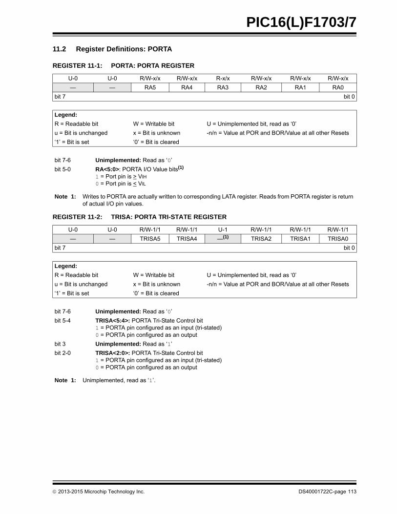
PIC16(L)F1703/7
11.2 Register Definitions: PORTA
REGISTER 11-1: PORTA: PORTA REGISTER
U-0 U-0 R/W-x/x R/W-x/x R-x/x R/W-x/x R/W-x/x R/W-x/x
— — RA5 RA4 RA3 RA2 RA1 RA0
bit 7 bit 0
Legend:
R = Readable bit W = Writable bit U = Unimplemented bit, read as ‘0’
u = Bit is unchanged x = Bit is unknown -n/n = Value at POR and BOR/Value at all other Resets
‘1’ = Bit is set ‘0’ = Bit is cleared
bit 7-6 Unimplemented: Read as ‘0’
bit 5-0 RA<5:0>: PORTA I/O Value bits(1)
1 = Port pin is > VIH
0 = Port pin is < VIL
Note 1: Writes to PORTA are actually written to corresponding LATA register. Reads from PORTA register is return of actual I/O pin values.
REGISTER 11-2: TRISA: PORTA TRI-STATE REGISTER
U-0 U-0 R/W-1/1 R/W-1/1 U-1 R/W-1/1 R/W-1/1 R/W-1/1
— — TRISA5 TRISA4 —(1) TRISA2 TRISA1 TRISA0
bit 7 bit 0
Legend:
R = Readable bit W = Writable bit U = Unimplemented bit, read as ‘0’
u = Bit is unchanged x = Bit is unknown -n/n = Value at POR and BOR/Value at all other Resets
‘1’ = Bit is set ‘0’ = Bit is cleared
bit 7-6 Unimplemented: Read as ‘0’
bit 5-4 TRISA<5:4>: PORTA Tri-State Control bit1 = PORTA pin configured as an input (tri-stated)0 = PORTA pin configured as an output
bit 3 Unimplemented: Read as ‘1’
bit 2-0 TRISA<2:0>: PORTA Tri-State Control bit1 = PORTA pin configured as an input (tri-stated)0 = PORTA pin configured as an output
Note 1: Unimplemented, read as ‘1’.
2013-2015 Microchip Technology Inc. DS40001722C-page 113
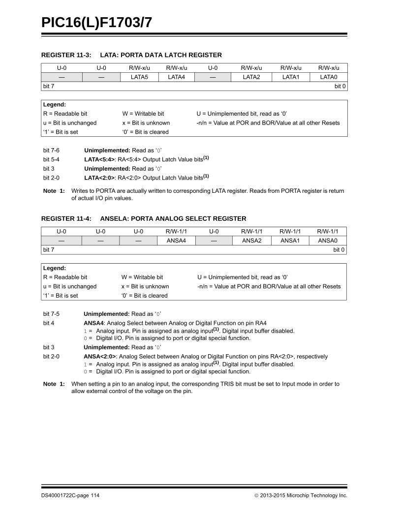
PIC16(L)F1703/7
REGISTER 11-3: LATA: PORTA DATA LATCH REGISTER
U-0 U-0 R/W-x/u R/W-x/u U-0 R/W-x/u R/W-x/u R/W-x/u
— — LATA5 LATA4 — LATA2 LATA1 LATA0
bit 7 bit 0
Legend:
R = Readable bit W = Writable bit U = Unimplemented bit, read as ‘0’
u = Bit is unchanged x = Bit is unknown -n/n = Value at POR and BOR/Value at all other Resets
‘1’ = Bit is set ‘0’ = Bit is cleared
bit 7-6 Unimplemented: Read as ‘0’
bit 5-4 LATA<5:4>: RA<5:4> Output Latch Value bits(1)
bit 3 Unimplemented: Read as ‘0’
bit 2-0 LATA<2:0>: RA<2:0> Output Latch Value bits(1)
Note 1: Writes to PORTA are actually written to corresponding LATA register. Reads from PORTA register is return of actual I/O pin values.
REGISTER 11-4: ANSELA: PORTA ANALOG SELECT REGISTER
U-0 U-0 U-0 R/W-1/1 U-0 R/W-1/1 R/W-1/1 R/W-1/1
— — — ANSA4 — ANSA2 ANSA1 ANSA0
bit 7 bit 0
Legend:
R = Readable bit W = Writable bit U = Unimplemented bit, read as ‘0’
u = Bit is unchanged x = Bit is unknown -n/n = Value at POR and BOR/Value at all other Resets
‘1’ = Bit is set ‘0’ = Bit is cleared
bit 7-5 Unimplemented: Read as ‘0’
bit 4 ANSA4: Analog Select between Analog or Digital Function on pin RA41 = Analog input. Pin is assigned as analog input(1). Digital input buffer disabled.0 = Digital I/O. Pin is assigned to port or digital special function.
bit 3 Unimplemented: Read as ‘0’
bit 2-0 ANSA<2:0>: Analog Select between Analog or Digital Function on pins RA<2:0>, respectively1 = Analog input. Pin is assigned as analog input(1). Digital input buffer disabled.0 = Digital I/O. Pin is assigned to port or digital special function.
Note 1: When setting a pin to an analog input, the corresponding TRIS bit must be set to Input mode in order to allow external control of the voltage on the pin.
DS40001722C-page 114 2013-2015 Microchip Technology Inc.
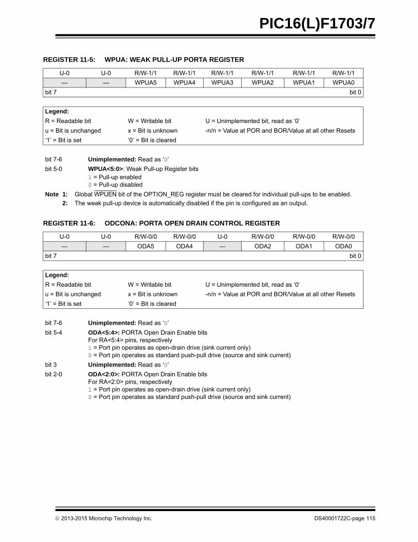
PIC16(L)F1703/7
REGISTER 11-5: WPUA: WEAK PULL-UP PORTA REGISTER
U-0 U-0 R/W-1/1 R/W-1/1 R/W-1/1 R/W-1/1 R/W-1/1 R/W-1/1
— — WPUA5 WPUA4 WPUA3 WPUA2 WPUA1 WPUA0
bit 7 bit 0
Legend:
R = Readable bit W = Writable bit U = Unimplemented bit, read as ‘0’
u = Bit is unchanged x = Bit is unknown -n/n = Value at POR and BOR/Value at all other Resets
‘1’ = Bit is set ‘0’ = Bit is cleared
bit 7-6 Unimplemented: Read as ‘0’
bit 5-0 WPUA<5:0>: Weak Pull-up Register bits1 = Pull-up enabled0 = Pull-up disabled
Note 1: Global WPUEN bit of the OPTION_REG register must be cleared for individual pull-ups to be enabled.
2: The weak pull-up device is automatically disabled if the pin is configured as an output.
REGISTER 11-6: ODCONA: PORTA OPEN DRAIN CONTROL REGISTER
U-0 U-0 R/W-0/0 R/W-0/0 U-0 R/W-0/0 R/W-0/0 R/W-0/0
— — ODA5 ODA4 — ODA2 ODA1 ODA0
bit 7 bit 0
Legend:
R = Readable bit W = Writable bit U = Unimplemented bit, read as ‘0’
u = Bit is unchanged x = Bit is unknown -n/n = Value at POR and BOR/Value at all other Resets
‘1’ = Bit is set ‘0’ = Bit is cleared
bit 7-6 Unimplemented: Read as ‘0’
bit 5-4 ODA<5:4>: PORTA Open Drain Enable bitsFor RA<5:4> pins, respectively1 = Port pin operates as open-drain drive (sink current only)0 = Port pin operates as standard push-pull drive (source and sink current)
bit 3 Unimplemented: Read as ‘0’
bit 2-0 ODA<2:0>: PORTA Open Drain Enable bitsFor RA<2:0> pins, respectively1 = Port pin operates as open-drain drive (sink current only)0 = Port pin operates as standard push-pull drive (source and sink current)
2013-2015 Microchip Technology Inc. DS40001722C-page 115
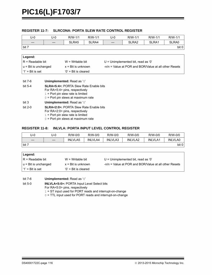
PIC16(L)F1703/7
REGISTER 11-7: SLRCONA: PORTA SLEW RATE CONTROL REGISTER
U-0 U-0 R/W-1/1 R/W-1/1 U-0 R/W-1/1 R/W-1/1 R/W-1/1
— — SLRA5 SLRA4 — SLRA2 SLRA1 SLRA0
bit 7 bit 0
Legend:
R = Readable bit W = Writable bit U = Unimplemented bit, read as ‘0’
u = Bit is unchanged x = Bit is unknown -n/n = Value at POR and BOR/Value at all other Resets
‘1’ = Bit is set ‘0’ = Bit is cleared
bit 7-6 Unimplemented: Read as ‘0’
bit 5-4 SLRA<5:4>: PORTA Slew Rate Enable bitsFor RA<5:4> pins, respectively1 = Port pin slew rate is limited0 = Port pin slews at maximum rate
bit 3 Unimplemented: Read as ‘0’
bit 2-0 SLRA<2:0>: PORTA Slew Rate Enable bitsFor RA<2:0> pins, respectively1 = Port pin slew rate is limited0 = Port pin slews at maximum rate
REGISTER 11-8: INLVLA: PORTA INPUT LEVEL CONTROL REGISTER
U-0 U-0 R/W-0/0 R/W-0/0 R/W-0/0 R/W-0/0 R/W-0/0 R/W-0/0
— — INLVLA5 INLVLA4 INLVLA3 INLVLA2 INLVLA1 INLVLA0
bit 7 bit 0
Legend:
R = Readable bit W = Writable bit U = Unimplemented bit, read as ‘0’
u = Bit is unchanged x = Bit is unknown -n/n = Value at POR and BOR/Value at all other Resets
‘1’ = Bit is set ‘0’ = Bit is cleared
bit 7-6 Unimplemented: Read as ‘0’
bit 5-0 INLVLA<5:0>: PORTA Input Level Select bitsFor RA<5:0> pins, respectively1 = ST input used for PORT reads and interrupt-on-change0 = TTL input used for PORT reads and interrupt-on-change
DS40001722C-page 116 2013-2015 Microchip Technology Inc.

PIC16(L)F1703/7
TABLE 11-2: SUMMARY OF REGISTERS ASSOCIATED WITH PORTA
TABLE 11-3: SUMMARY OF CONFIGURATION BITS ASSOCIATED WITH PORTA
Name Bit 7 Bit 6 Bit 5 Bit 4 Bit 3 Bit 2 Bit 1 Bit 0Register on Page
ANSELA — — — ANSA4 — ANSA2 ANSA1 ANSA0 114
INLVLA — — INLVLA5 INLVLA4 INLVLA3 INLVLA2 INLVLA1 INLVLA0 116
LATA — — LATA5 LATA4 — LATA2 LATA1 LATA0 114
ODCONA — — ODA5 ODA4 — ODA2 ODA1 ODA0 115
OPTION_REG WPUEN INTEDG TMR0CS TMR0SE PSA PS<2:0> 168
PORTA — — RA5 RA4 RA3 RA2 RA1 RA0 113
SLRCONA — — SLRA5 SLRA4 — SLRA2 SLRA1 SLRA0 116
TRISA — — TRISA5 TRISA4 —(1) TRISA2 TRISA1 TRISA0 113
WPUA — — WPUA5 WPUA4 WPUA3 WPUA2 WPUA1 WPUA0 115
Legend: x = unknown, u = unchanged, – = unimplemented locations read as ‘0’. Shaded cells are not used by PORTA.Note 1: Unimplemented, read as ‘1’.
Name Bits Bit -/7 Bit -/6 Bit 13/5 Bit 12/4 Bit 11/3 Bit 10/2 Bit 9/1 Bit 8/0Register on Page
CONFIG113:8 — — — — CLKOUTEN BOREN<1:0> —
497:0 CP MCLRE PWRTE WDTE<1:0> — FOSC<1:0>
CONFIG213:8 — — LVP DEBUG LPBOR BORV STVREN PLLEN
507:0 ZCDDIS — — — — PPS1WAY WRT<1:0>
Legend: — = unimplemented location, read as ‘0’. Shaded cells are not used by PORTA.
2013-2015 Microchip Technology Inc. DS40001722C-page 117
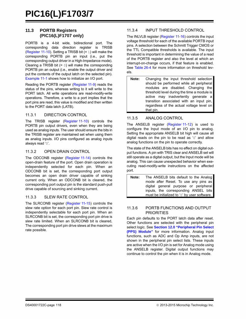
PIC16(L)F1703/7
11.3 PORTB Registers(PIC16(L)F1707 only)
PORTB is a 4-bit wide, bidirectional port. Thecorresponding data direction register is TRISB(Register 11-10). Setting a TRISB bit (= 1) will make thecorresponding PORTB pin an input (i.e., put thecorresponding output driver in a High-Impedance mode).Clearing a TRISB bit (= 0) will make the correspondingPORTB pin an output (i.e., enable the output driver andput the contents of the output latch on the selected pin).Example 11-1 shows how to initialize an I/O port.
Reading the PORTB register (Register 11-9) reads thestatus of the pins, whereas writing to it will write to thePORT latch. All write operations are read-modify-writeoperations. Therefore, a write to a port implies that theport pins are read, this value is modified and then writtento the PORT data latch (LATB).
11.3.1 DIRECTION CONTROL
The TRISB register (Register 11-10) controls thePORTB pin output drivers, even when they are beingused as analog inputs. The user should ensure the bits inthe TRISB register are maintained set when using themas analog inputs. I/O pins configured as analog inputsalways read ‘0’.
11.3.2 OPEN DRAIN CONTROL
The ODCONB register (Register 11-14) controls theopen-drain feature of the port. Open drain operation isindependently selected for each pin. When anODCONB bit is set, the corresponding port outputbecomes an open drain driver capable of sinkingcurrent only. When an ODCONB bit is cleared, thecorresponding port output pin is the standard push-pulldrive capable of sourcing and sinking current.
11.3.3 SLEW RATE CONTROL
The SLRCONB register (Register 11-15) controls theslew rate option for each port pin. Slew rate control isindependently selectable for each port pin. When anSLRCONB bit is set, the corresponding port pin drive isslew rate limited. When an SLRCONB bit is cleared,The corresponding port pin drive slews at the maximumrate possible.
11.3.4 INPUT THRESHOLD CONTROL
The INLVLB register (Register 11-16) controls the inputvoltage threshold for each of the available PORTB inputpins. A selection between the Schmitt Trigger CMOS orthe TTL Compatible thresholds is available. The inputthreshold is important in determining the value of a readof the PORTB register and also the level at which aninterrupt-on-change occurs, if that feature is enabled.See Table 26-4 for more information on threshold lev-els.
11.3.5 ANALOG CONTROL
The ANSELB register (Register 11-12) is used toconfigure the Input mode of an I/O pin to analog.Setting the appropriate ANSELB bit high will cause alldigital reads on the pin to be read as ‘0’ and allowanalog functions on the pin to operate correctly.
The state of the ANSELB bits has no effect on digital out-put functions. A pin with TRIS clear and ANSELB set willstill operate as a digital output, but the Input mode will beanalog. This can cause unexpected behavior when exe-cuting read-modify-write instructions on the affectedport.
11.3.6 PORTB FUNCTIONS AND OUTPUT PRIORITIES
Each pin defaults to the PORT latch data after reset.Other functions are selected with the peripheral pinselect logic. See Section 12.0 “Peripheral Pin Select(PPS) Module” for more information. Analog inputfunctions, such as ADC and Op Amp inputs, are notshown in the peripheral pin select lists. These inputsare active when the I/O pin is set for Analog mode usingthe ANSELB register. Digital output functions maycontinue to control the pin when it is in Analog mode.
Note: Changing the input threshold selectionshould be performed while all peripheralmodules are disabled. Changing thethreshold level during the time a module isactive may inadvertently generate atransition associated with an input pin,regardless of the actual voltage level onthat pin.
Note: The ANSELB bits default to the Analogmode after Reset. To use any pins asdigital general purpose or peripheralinputs, the corresponding ANSEL bitsmust be initialized to ‘0’ by user software.
DS40001722C-page 118 2013-2015 Microchip Technology Inc.
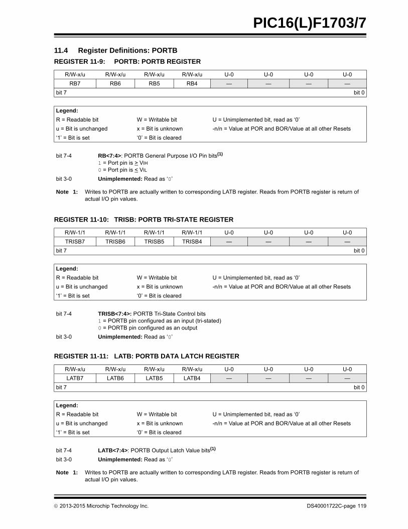
PIC16(L)F1703/7
11.4 Register Definitions: PORTB
REGISTER 11-9: PORTB: PORTB REGISTER
R/W-x/u R/W-x/u R/W-x/u R/W-x/u U-0 U-0 U-0 U-0
RB7 RB6 RB5 RB4 — — — —
bit 7 bit 0
Legend:
R = Readable bit W = Writable bit U = Unimplemented bit, read as ‘0’
u = Bit is unchanged x = Bit is unknown -n/n = Value at POR and BOR/Value at all other Resets
‘1’ = Bit is set ‘0’ = Bit is cleared
bit 7-4 RB<7:4>: PORTB General Purpose I/O Pin bits(1)
1 = Port pin is > VIH
0 = Port pin is < VIL
bit 3-0 Unimplemented: Read as ‘0’
Note 1: Writes to PORTB are actually written to corresponding LATB register. Reads from PORTB register is return of actual I/O pin values.
REGISTER 11-10: TRISB: PORTB TRI-STATE REGISTER
R/W-1/1 R/W-1/1 R/W-1/1 R/W-1/1 U-0 U-0 U-0 U-0
TRISB7 TRISB6 TRISB5 TRISB4 — — — —
bit 7 bit 0
Legend:
R = Readable bit W = Writable bit U = Unimplemented bit, read as ‘0’
u = Bit is unchanged x = Bit is unknown -n/n = Value at POR and BOR/Value at all other Resets
‘1’ = Bit is set ‘0’ = Bit is cleared
bit 7-4 TRISB<7:4>: PORTB Tri-State Control bits1 = PORTB pin configured as an input (tri-stated)0 = PORTB pin configured as an output
bit 3-0 Unimplemented: Read as ‘0’
REGISTER 11-11: LATB: PORTB DATA LATCH REGISTER
R/W-x/u R/W-x/u R/W-x/u R/W-x/u U-0 U-0 U-0 U-0
LATB7 LATB6 LATB5 LATB4 — — — —
bit 7 bit 0
Legend:
R = Readable bit W = Writable bit U = Unimplemented bit, read as ‘0’
u = Bit is unchanged x = Bit is unknown -n/n = Value at POR and BOR/Value at all other Resets
‘1’ = Bit is set ‘0’ = Bit is cleared
bit 7-4 LATB<7:4>: PORTB Output Latch Value bits(1)
bit 3-0 Unimplemented: Read as ‘0’
Note 1: Writes to PORTB are actually written to corresponding LATB register. Reads from PORTB register is return of actual I/O pin values.
2013-2015 Microchip Technology Inc. DS40001722C-page 119
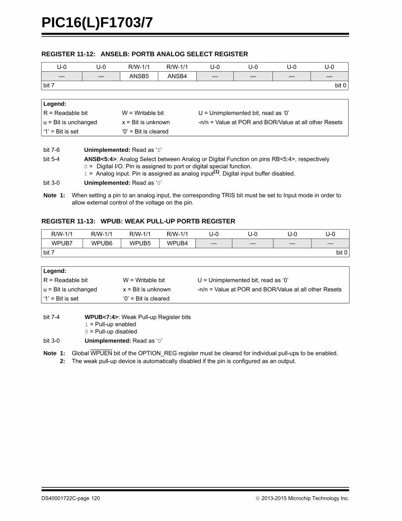
PIC16(L)F1703/7
REGISTER 11-12: ANSELB: PORTB ANALOG SELECT REGISTER
U-0 U-0 R/W-1/1 R/W-1/1 U-0 U-0 U-0 U-0
— — ANSB5 ANSB4 — — — —
bit 7 bit 0
Legend:
R = Readable bit W = Writable bit U = Unimplemented bit, read as ‘0’
u = Bit is unchanged x = Bit is unknown -n/n = Value at POR and BOR/Value at all other Resets
‘1’ = Bit is set ‘0’ = Bit is cleared
bit 7-6 Unimplemented: Read as ‘0’
bit 5-4 ANSB<5:4>: Analog Select between Analog or Digital Function on pins RB<5:4>, respectively0 = Digital I/O. Pin is assigned to port or digital special function.1 = Analog input. Pin is assigned as analog input(1). Digital input buffer disabled.
bit 3-0 Unimplemented: Read as ‘0’
Note 1: When setting a pin to an analog input, the corresponding TRIS bit must be set to Input mode in order to allow external control of the voltage on the pin.
REGISTER 11-13: WPUB: WEAK PULL-UP PORTB REGISTER
R/W-1/1 R/W-1/1 R/W-1/1 R/W-1/1 U-0 U-0 U-0 U-0
WPUB7 WPUB6 WPUB5 WPUB4 — — — —
bit 7 bit 0
Legend:
R = Readable bit W = Writable bit U = Unimplemented bit, read as ‘0’
u = Bit is unchanged x = Bit is unknown -n/n = Value at POR and BOR/Value at all other Resets
‘1’ = Bit is set ‘0’ = Bit is cleared
bit 7-4 WPUB<7:4>: Weak Pull-up Register bits1 = Pull-up enabled0 = Pull-up disabled
bit 3-0 Unimplemented: Read as ‘0’
Note 1: Global WPUEN bit of the OPTION_REG register must be cleared for individual pull-ups to be enabled.2: The weak pull-up device is automatically disabled if the pin is configured as an output.
DS40001722C-page 120 2013-2015 Microchip Technology Inc.

PIC16(L)F1703/7
REGISTER 11-14: ODCONB: PORTB OPEN DRAIN CONTROL REGISTER
R/W-0/0 R/W-0/0 R/W-0/0 R/W-0/0 U-0 U-0 U-0 U-0
ODB7 ODB6 ODB5 ODB4 — — — —
bit 7 bit 0
Legend:
R = Readable bit W = Writable bit U = Unimplemented bit, read as ‘0’
u = Bit is unchanged x = Bit is unknown -n/n = Value at POR and BOR/Value at all other Resets
‘1’ = Bit is set ‘0’ = Bit is cleared
bit 7-4 ODB<7:4>: PORTB Open Drain Enable bitsFor RB<7:4> pins, respectively1 = Port pin operates as open-drain drive (sink current only)0 = Port pin operates as standard push-pull drive (source and sink current)
bit 3-0 Unimplemented: Read as ‘0’
REGISTER 11-15: SLRCONB: PORTB SLEW RATE CONTROL REGISTER
R/W-1/1 R/W-1/1 R/W-1/1 R/W-1/1 U-0 U-0 U-0 U-0
SLRB7 SLRB6 SLRB5 SLRB4 — — — —
bit 7 bit 0
Legend:
R = Readable bit W = Writable bit U = Unimplemented bit, read as ‘0’
u = Bit is unchanged x = Bit is unknown -n/n = Value at POR and BOR/Value at all other Resets
‘1’ = Bit is set ‘0’ = Bit is cleared
bit 7-4 SLRB<7:4>: PORTB Slew Rate Enable bitsFor RB<7:4> pins, respectively1 = Port pin slew rate is limited0 = Port pin slews at maximum rate
bit 3-0 Unimplemented: Read as ‘0’
REGISTER 11-16: INLVLB: PORTB INPUT LEVEL CONTROL REGISTER
R/W-0/0 R/W-0/0 R/W-0/0 R/W-0/0 U-0 U-0 U-0 U-0
INLVLB7 INLVLB6 INLVLB5 INLVLB4 — — — —
bit 7 bit 0
Legend:
R = Readable bit W = Writable bit U = Unimplemented bit, read as ‘0’
u = Bit is unchanged x = Bit is unknown -n/n = Value at POR and BOR/Value at all other Resets
‘1’ = Bit is set ‘0’ = Bit is cleared
bit 7-4 INLVLB<7:4>: PORTB Input Level Select bitsFor RB<7:4> pins, respectively1 = ST input used for PORT reads and interrupt-on-change0 = TTL input used for PORT reads and interrupt-on-change
bit 3-0 Unimplemented: Read as ‘0’
2013-2015 Microchip Technology Inc. DS40001722C-page 121
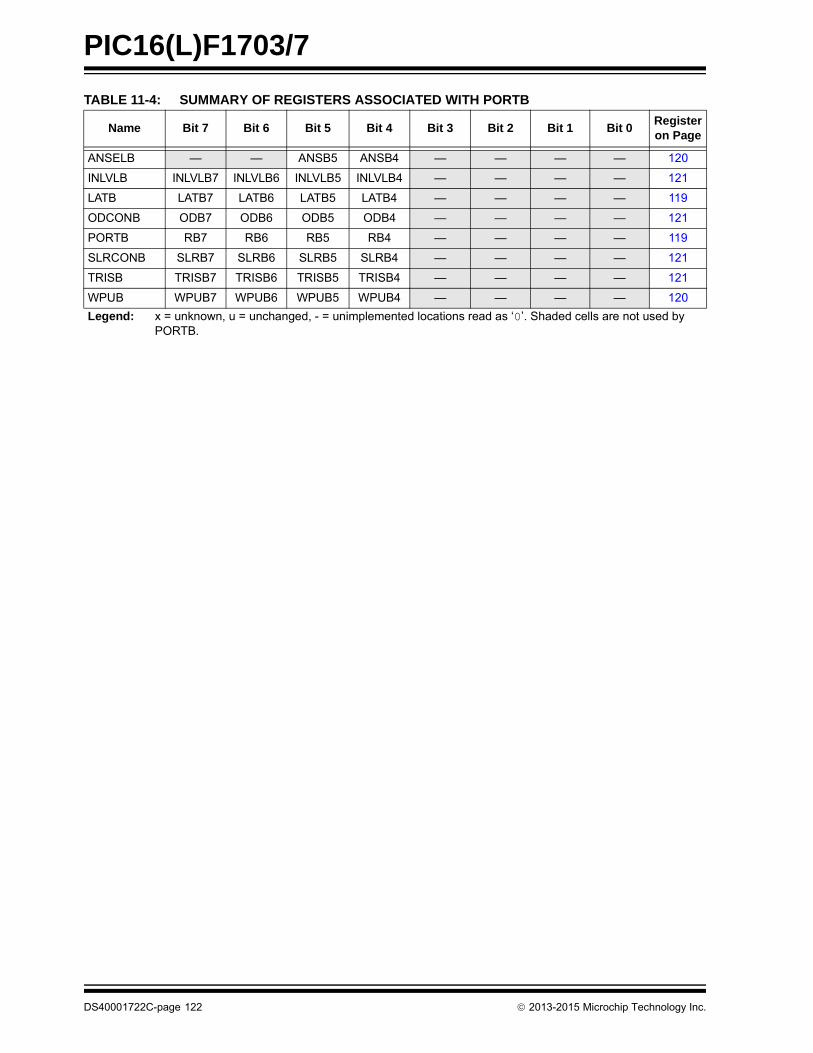
PIC16(L)F1703/7
TABLE 11-4: SUMMARY OF REGISTERS ASSOCIATED WITH PORTB
Name Bit 7 Bit 6 Bit 5 Bit 4 Bit 3 Bit 2 Bit 1 Bit 0Register on Page
ANSELB — — ANSB5 ANSB4 — — — — 120
INLVLB INLVLB7 INLVLB6 INLVLB5 INLVLB4 — — — — 121
LATB LATB7 LATB6 LATB5 LATB4 — — — — 119
ODCONB ODB7 ODB6 ODB5 ODB4 — — — — 121
PORTB RB7 RB6 RB5 RB4 — — — — 119
SLRCONB SLRB7 SLRB6 SLRB5 SLRB4 — — — — 121
TRISB TRISB7 TRISB6 TRISB5 TRISB4 — — — — 121
WPUB WPUB7 WPUB6 WPUB5 WPUB4 — — — — 120
Legend: x = unknown, u = unchanged, - = unimplemented locations read as ‘0’. Shaded cells are not used by PORTB.
DS40001722C-page 122 2013-2015 Microchip Technology Inc.
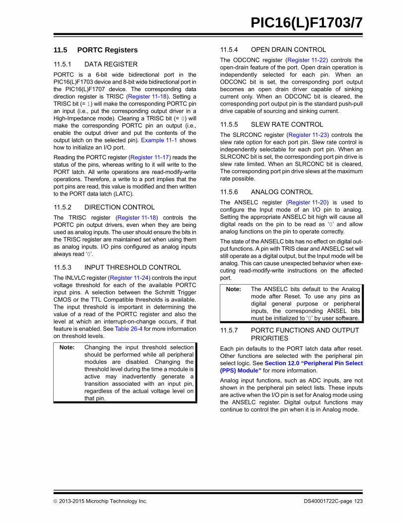
PIC16(L)F1703/7
11.5 PORTC Registers
11.5.1 DATA REGISTER
PORTC is a 6-bit wide bidirectional port in thePIC16(L)F1703 device and 8-bit wide bidirectional port inthe PIC16(L)F1707 device. The corresponding datadirection register is TRISC (Register 11-18). Setting aTRISC bit (= 1) will make the corresponding PORTC pinan input (i.e., put the corresponding output driver in aHigh-Impedance mode). Clearing a TRISC bit (= 0) willmake the corresponding PORTC pin an output (i.e.,enable the output driver and put the contents of theoutput latch on the selected pin). Example 11-1 showshow to initialize an I/O port.
Reading the PORTC register (Register 11-17) reads thestatus of the pins, whereas writing to it will write to thePORT latch. All write operations are read-modify-writeoperations. Therefore, a write to a port implies that theport pins are read, this value is modified and then writtento the PORT data latch (LATC).
11.5.2 DIRECTION CONTROL
The TRISC register (Register 11-18) controls thePORTC pin output drivers, even when they are beingused as analog inputs. The user should ensure the bits inthe TRISC register are maintained set when using themas analog inputs. I/O pins configured as analog inputsalways read ‘0’.
11.5.3 INPUT THRESHOLD CONTROL
The INLVLC register (Register 11-24) controls the inputvoltage threshold for each of the available PORTCinput pins. A selection between the Schmitt TriggerCMOS or the TTL Compatible thresholds is available.The input threshold is important in determining thevalue of a read of the PORTC register and also thelevel at which an interrupt-on-change occurs, if thatfeature is enabled. See Table 26-4 for more informationon threshold levels.
11.5.4 OPEN DRAIN CONTROL
The ODCONC register (Register 11-22) controls theopen-drain feature of the port. Open drain operation isindependently selected for each pin. When anODCONC bit is set, the corresponding port outputbecomes an open drain driver capable of sinkingcurrent only. When an ODCONC bit is cleared, thecorresponding port output pin is the standard push-pulldrive capable of sourcing and sinking current.
11.5.5 SLEW RATE CONTROL
The SLRCONC register (Register 11-23) controls theslew rate option for each port pin. Slew rate control isindependently selectable for each port pin. When anSLRCONC bit is set, the corresponding port pin drive isslew rate limited. When an SLRCONC bit is cleared,The corresponding port pin drive slews at the maximumrate possible.
11.5.6 ANALOG CONTROL
The ANSELC register (Register 11-20) is used toconfigure the Input mode of an I/O pin to analog.Setting the appropriate ANSELC bit high will cause alldigital reads on the pin to be read as ‘0’ and allowanalog functions on the pin to operate correctly.
The state of the ANSELC bits has no effect on digital out-put functions. A pin with TRIS clear and ANSELC set willstill operate as a digital output, but the Input mode will beanalog. This can cause unexpected behavior when exe-cuting read-modify-write instructions on the affectedport.
11.5.7 PORTC FUNCTIONS AND OUTPUT PRIORITIES
Each pin defaults to the PORT latch data after reset.Other functions are selected with the peripheral pinselect logic. See Section 12.0 “Peripheral Pin Select(PPS) Module” for more information.
Analog input functions, such as ADC inputs, are notshown in the peripheral pin select lists. These inputsare active when the I/O pin is set for Analog mode usingthe ANSELC register. Digital output functions maycontinue to control the pin when it is in Analog mode.
Note: Changing the input threshold selectionshould be performed while all peripheralmodules are disabled. Changing thethreshold level during the time a module isactive may inadvertently generate atransition associated with an input pin,regardless of the actual voltage level onthat pin.
Note: The ANSELC bits default to the Analogmode after Reset. To use any pins asdigital general purpose or peripheralinputs, the corresponding ANSEL bitsmust be initialized to ‘0’ by user software.
2013-2015 Microchip Technology Inc. DS40001722C-page 123
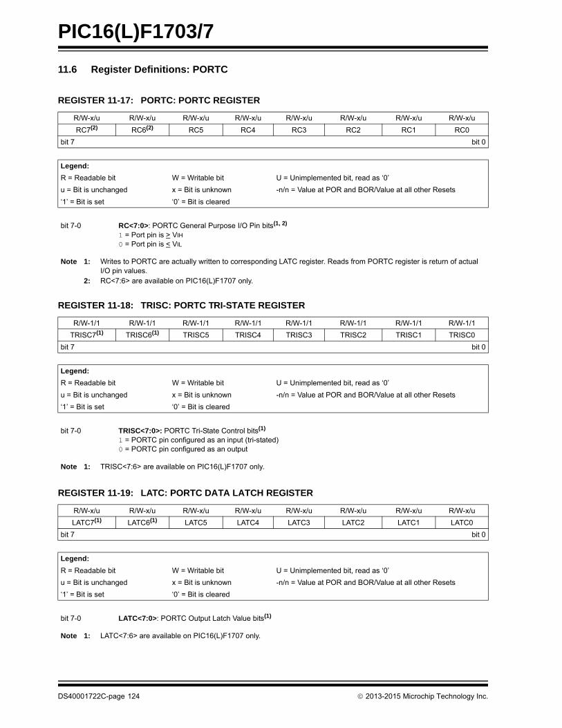
PIC16(L)F1703/7
11.6 Register Definitions: PORTC
REGISTER 11-17: PORTC: PORTC REGISTER
R/W-x/u R/W-x/u R/W-x/u R/W-x/u R/W-x/u R/W-x/u R/W-x/u R/W-x/u
RC7(2) RC6(2) RC5 RC4 RC3 RC2 RC1 RC0
bit 7 bit 0
Legend:
R = Readable bit W = Writable bit U = Unimplemented bit, read as ‘0’
u = Bit is unchanged x = Bit is unknown -n/n = Value at POR and BOR/Value at all other Resets
‘1’ = Bit is set ‘0’ = Bit is cleared
bit 7-0 RC<7:0>: PORTC General Purpose I/O Pin bits(1, 2)
1 = Port pin is > VIH
0 = Port pin is < VIL
Note 1: Writes to PORTC are actually written to corresponding LATC register. Reads from PORTC register is return of actual I/O pin values.
2: RC<7:6> are available on PIC16(L)F1707 only.
REGISTER 11-18: TRISC: PORTC TRI-STATE REGISTER
R/W-1/1 R/W-1/1 R/W-1/1 R/W-1/1 R/W-1/1 R/W-1/1 R/W-1/1 R/W-1/1
TRISC7(1) TRISC6(1) TRISC5 TRISC4 TRISC3 TRISC2 TRISC1 TRISC0
bit 7 bit 0
Legend:
R = Readable bit W = Writable bit U = Unimplemented bit, read as ‘0’
u = Bit is unchanged x = Bit is unknown -n/n = Value at POR and BOR/Value at all other Resets
‘1’ = Bit is set ‘0’ = Bit is cleared
bit 7-0 TRISC<7:0>: PORTC Tri-State Control bits(1)
1 = PORTC pin configured as an input (tri-stated)0 = PORTC pin configured as an output
Note 1: TRISC<7:6> are available on PIC16(L)F1707 only.
REGISTER 11-19: LATC: PORTC DATA LATCH REGISTER
R/W-x/u R/W-x/u R/W-x/u R/W-x/u R/W-x/u R/W-x/u R/W-x/u R/W-x/u
LATC7(1) LATC6(1) LATC5 LATC4 LATC3 LATC2 LATC1 LATC0
bit 7 bit 0
Legend:
R = Readable bit W = Writable bit U = Unimplemented bit, read as ‘0’
u = Bit is unchanged x = Bit is unknown -n/n = Value at POR and BOR/Value at all other Resets
‘1’ = Bit is set ‘0’ = Bit is cleared
bit 7-0 LATC<7:0>: PORTC Output Latch Value bits(1)
Note 1: LATC<7:6> are available on PIC16(L)F1707 only.
DS40001722C-page 124 2013-2015 Microchip Technology Inc.
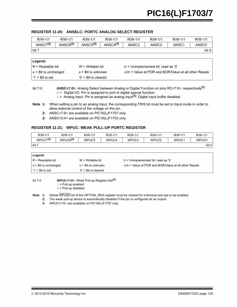
PIC16(L)F1703/7
REGISTER 11-20: ANSELC: PORTC ANALOG SELECT REGISTER
R/W-1/1 R/W-1/1 R/W-1/1 R/W-1/1 R/W-1/1 R/W-1/1 R/W-1/1 R/W-1/1
ANSC7(2) ANSC6(2) ANSC5(3) ANSC4(3) ANSC3 ANSC2 ANSC1 ANSC0
bit 7 bit 0
Legend:
R = Readable bit W = Writable bit U = Unimplemented bit, read as ‘0’
u = Bit is unchanged x = Bit is unknown -n/n = Value at POR and BOR/Value at all other Resets
‘1’ = Bit is set ‘0’ = Bit is cleared
bit 7-0 ANSC<7:0>: Analog Select between Analog or Digital Function on pins RC<7:0>, respectively(1)
0 = Digital I/O. Pin is assigned to port or digital special function.1 = Analog input. Pin is assigned as analog input(1). Digital input buffer disabled.
Note 1: When setting a pin to an analog input, the corresponding TRIS bit must be set to Input mode in order to allow external control of the voltage on the pin.
2: ANSC<7:6> are available on PIC16(L)F1707 only.
3: ANSC<5:4> are available on PIC16(L)F1703 only.
REGISTER 11-21: WPUC: WEAK PULL-UP PORTC REGISTER
R/W-1/1 R/W-1/1 R/W-1/1 R/W-1/1 R/W-1/1 R/W-1/1 R/W-1/1 R/W-1/1
WPUC7(3) WPUC6(3) WPUC5 WPUC4 WPUC3 WPUC2 WPUC1 WPUC0
bit 7 bit 0
Legend:
R = Readable bit W = Writable bit U = Unimplemented bit, read as ‘0’
u = Bit is unchanged x = Bit is unknown -n/n = Value at POR and BOR/Value at all other Resets
‘1’ = Bit is set ‘0’ = Bit is cleared
bit 7-0 WPUC<7:0>: Weak Pull-up Register bits(3)
1 = Pull-up enabled0 = Pull-up disabled
Note 1: Global WPUEN bit of the OPTION_REG register must be cleared for individual pull-ups to be enabled.2: The weak pull-up device is automatically disabled if the pin is configured as an output.3: WPUC<7:6> are available on PIC16(L)F1707 only.
2013-2015 Microchip Technology Inc. DS40001722C-page 125
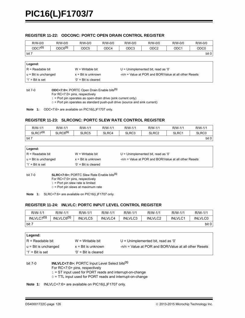
PIC16(L)F1703/7
REGISTER 11-22: ODCONC: PORTC OPEN DRAIN CONTROL REGISTER
R/W-0/0 R/W-0/0 R/W-0/0 R/W-0/0 R/W-0/0 R/W-0/0 R/W-0/0 R/W-0/0
ODC7(1) ODC6(1) ODC5 ODC4 ODC3 ODC2 ODC1 ODC0
bit 7 bit 0
Legend:
R = Readable bit W = Writable bit U = Unimplemented bit, read as ‘0’
u = Bit is unchanged x = Bit is unknown -n/n = Value at POR and BOR/Value at all other Resets
‘1’ = Bit is set ‘0’ = Bit is cleared
bit 7-0 ODC<7:0>: PORTC Open Drain Enable bits(1)
For RC<7:0> pins, respectively1 = Port pin operates as open-drain drive (sink current only)0 = Port pin operates as standard push-pull drive (source and sink current)
Note 1: ODC<7:6> are available on PIC16(L)F1707 only.
REGISTER 11-23: SLRCONC: PORTC SLEW RATE CONTROL REGISTER
R/W-1/1 R/W-1/1 R/W-1/1 R/W-1/1 R/W-1/1 R/W-1/1 R/W-1/1 R/W-1/1
SLRC7(1) SLRC6(1) SLRC5 SLRC4 SLRC3 SLRC2 SLRC1 SLRC0
bit 7 bit 0
Legend:
R = Readable bit W = Writable bit U = Unimplemented bit, read as ‘0’
u = Bit is unchanged x = Bit is unknown -n/n = Value at POR and BOR/Value at all other Resets
‘1’ = Bit is set ‘0’ = Bit is cleared
bit 7-0 SLRC<7:0>: PORTC Slew Rate Enable bits(1)
For RC<7:0> pins, respectively1 = Port pin slew rate is limited0 = Port pin slews at maximum rate
Note 1: SLRC<7:6> are available on PIC16(L)F1707 only.
REGISTER 11-24: INLVLC: PORTC INPUT LEVEL CONTROL REGISTER
R/W-1/1 R/W-1/1 R/W-1/1 R/W-1/1 R/W-1/1 R/W-1/1 R/W-1/1 R/W-1/1
INLVLC7(1) INLVLC6(1) INLVLC5 INLVLC4 INLVLC3 INLVLC2 INLVLC1 INLVLC0
bit 7 bit 0
Legend:
R = Readable bit W = Writable bit U = Unimplemented bit, read as ‘0’
u = Bit is unchanged x = Bit is unknown -n/n = Value at POR and BOR/Value at all other Resets
‘1’ = Bit is set ‘0’ = Bit is cleared
bit 7-0 INLVLC<7:0>: PORTC Input Level Select bits(1)
For RC<7:0> pins, respectively1 = ST input used for PORT reads and interrupt-on-change0 = TTL input used for PORT reads and interrupt-on-change
Note 1: INLVLC<7:6> are available on PIC16(L)F1707 only.
DS40001722C-page 126 2013-2015 Microchip Technology Inc.
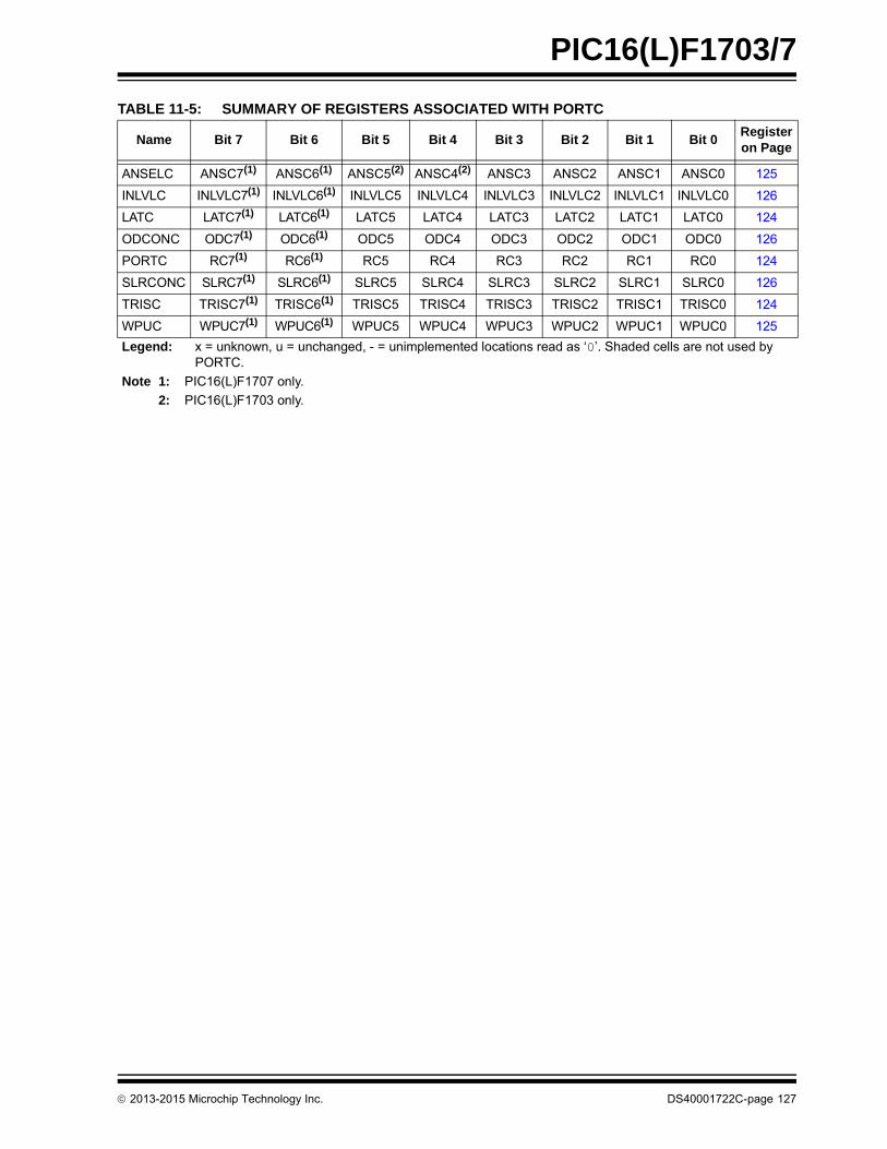
PIC16(L)F1703/7
TABLE 11-5: SUMMARY OF REGISTERS ASSOCIATED WITH PORTC
Name Bit 7 Bit 6 Bit 5 Bit 4 Bit 3 Bit 2 Bit 1 Bit 0Register on Page
ANSELC ANSC7(1) ANSC6(1) ANSC5(2) ANSC4(2) ANSC3 ANSC2 ANSC1 ANSC0 125
INLVLC INLVLC7(1) INLVLC6(1) INLVLC5 INLVLC4 INLVLC3 INLVLC2 INLVLC1 INLVLC0 126
LATC LATC7(1) LATC6(1) LATC5 LATC4 LATC3 LATC2 LATC1 LATC0 124
ODCONC ODC7(1) ODC6(1) ODC5 ODC4 ODC3 ODC2 ODC1 ODC0 126
PORTC RC7(1) RC6(1) RC5 RC4 RC3 RC2 RC1 RC0 124
SLRCONC SLRC7(1) SLRC6(1) SLRC5 SLRC4 SLRC3 SLRC2 SLRC1 SLRC0 126
TRISC TRISC7(1) TRISC6(1) TRISC5 TRISC4 TRISC3 TRISC2 TRISC1 TRISC0 124
WPUC WPUC7(1) WPUC6(1) WPUC5 WPUC4 WPUC3 WPUC2 WPUC1 WPUC0 125
Legend: x = unknown, u = unchanged, - = unimplemented locations read as ‘0’. Shaded cells are not used by PORTC.
Note 1: PIC16(L)F1707 only.
2: PIC16(L)F1703 only.
2013-2015 Microchip Technology Inc. DS40001722C-page 127
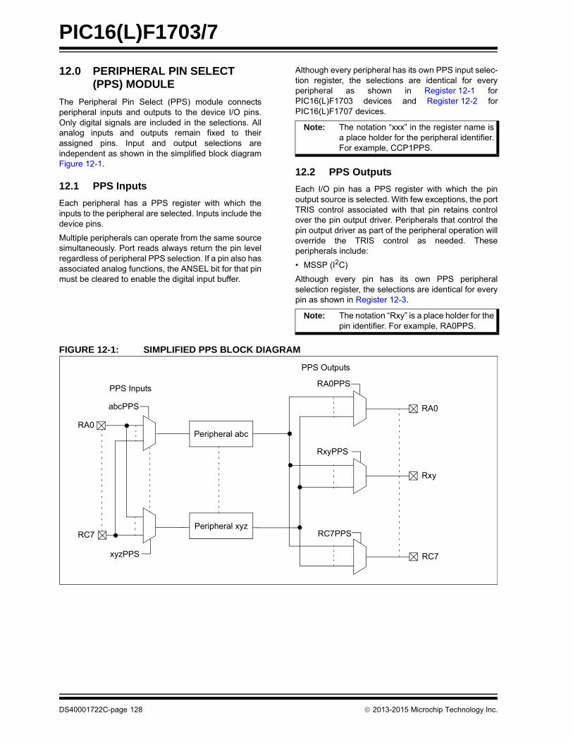
PIC16(L)F1703/7
12.0 PERIPHERAL PIN SELECT (PPS) MODULE
The Peripheral Pin Select (PPS) module connectsperipheral inputs and outputs to the device I/O pins.Only digital signals are included in the selections. Allanalog inputs and outputs remain fixed to theirassigned pins. Input and output selections areindependent as shown in the simplified block diagramFigure 12-1.
12.1 PPS Inputs
Each peripheral has a PPS register with which theinputs to the peripheral are selected. Inputs include thedevice pins.
Multiple peripherals can operate from the same sourcesimultaneously. Port reads always return the pin levelregardless of peripheral PPS selection. If a pin also hasassociated analog functions, the ANSEL bit for that pinmust be cleared to enable the digital input buffer.
Although every peripheral has its own PPS input selec-tion register, the selections are identical for everyperipheral as shown in Register 12-1 forPIC16(L)F1703 devices and Register 12-2 forPIC16(L)F1707 devices.
12.2 PPS Outputs
Each I/O pin has a PPS register with which the pinoutput source is selected. With few exceptions, the portTRIS control associated with that pin retains controlover the pin output driver. Peripherals that control thepin output driver as part of the peripheral operation willoverride the TRIS control as needed. Theseperipherals include:
• MSSP (I2C)
Although every pin has its own PPS peripheralselection register, the selections are identical for everypin as shown in Register 12-3.
FIGURE 12-1: SIMPLIFIED PPS BLOCK DIAGRAM
Note: The notation “xxx” in the register name isa place holder for the peripheral identifier.For example, CCP1PPS.
Note: The notation “Rxy” is a place holder for thepin identifier. For example, RA0PPS.
RA0
Rxy
RA0PPS
RxyPPS
RC7
RC7PPS
PPS Outputs
PPS Inputs
Peripheral abc
Peripheral xyz
abcPPS
xyzPPS
RA0
RC7
DS40001722C-page 128 2013-2015 Microchip Technology Inc.
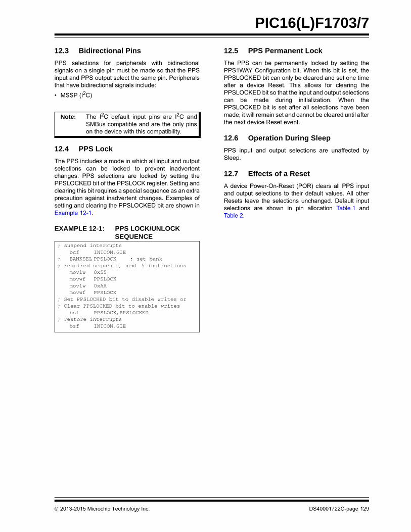
PIC16(L)F1703/7
12.3 Bidirectional Pins
PPS selections for peripherals with bidirectionalsignals on a single pin must be made so that the PPSinput and PPS output select the same pin. Peripheralsthat have bidirectional signals include:
• MSSP (I2C)
12.4 PPS Lock
The PPS includes a mode in which all input and outputselections can be locked to prevent inadvertentchanges. PPS selections are locked by setting thePPSLOCKED bit of the PPSLOCK register. Setting andclearing this bit requires a special sequence as an extraprecaution against inadvertent changes. Examples ofsetting and clearing the PPSLOCKED bit are shown inExample 12-1.
EXAMPLE 12-1: PPS LOCK/UNLOCK SEQUENCE
12.5 PPS Permanent Lock
The PPS can be permanently locked by setting thePPS1WAY Configuration bit. When this bit is set, thePPSLOCKED bit can only be cleared and set one timeafter a device Reset. This allows for clearing thePPSLOCKED bit so that the input and output selectionscan be made during initialization. When thePPSLOCKED bit is set after all selections have beenmade, it will remain set and cannot be cleared until afterthe next device Reset event.
12.6 Operation During Sleep
PPS input and output selections are unaffected bySleep.
12.7 Effects of a Reset
A device Power-On-Reset (POR) clears all PPS inputand output selections to their default values. All otherResets leave the selections unchanged. Default inputselections are shown in pin allocation Table 1 andTable 2.
Note: The I2C default input pins are I2C andSMBus compatible and are the only pinson the device with this compatibility.
; suspend interruptsbcf INTCON,GIE
; BANKSEL PPSLOCK ; set bank; required sequence, next 5 instructions
movlw 0x55movwf PPSLOCKmovlw 0xAAmovwf PPSLOCK
; Set PPSLOCKED bit to disable writes or; Clear PPSLOCKED bit to enable writes
bsf PPSLOCK,PPSLOCKED; restore interrupts
bsf INTCON,GIE
2013-2015 Microchip Technology Inc. DS40001722C-page 129

PIC16(L)F1703/7
12.8 Register Definitions: PPS Input Selection
REGISTER 12-1: xxxPPS: PERIPHERAL xxx INPUT SELECTION (PIC16(L)F1703)
U-0 U-0 U-0 R/W-q/u R/W-q/u R/W-q/u R/W-q/u R/W-q/u
— — — xxxPPS<4:0>
bit 7 bit 0
Legend:
R = Readable bit W = Writable bit U = Unimplemented bit, read as ‘0’
u = Bit is unchanged x = Bit is unknown -n/n = Value at POR and BOR/Value at all other Resets
‘1’ = Bit is set ‘0’ = Bit is cleared q = value depends on peripheral
bit 7-5 Unimplemented: Read as ‘0’
bit 4-0 xxxPPS<4:0>: Peripheral xxx Input Selection bits11xxx = Reserved. Do not use.
1011x = Reserved. Do not use.10101 = Peripheral input is RC510100 = Peripheral input is RC410011 = Peripheral input is RC310010 = Peripheral input is RC210001 = Peripheral input is RC110000 = Peripheral input is RC0
01xxx = Reserved. Do not use.
0011X = Reserved. Do not use.00101 = Peripheral input is RA500100 = Peripheral input is RA400011 = Peripheral input is RA300010 = Peripheral input is RA200001 = Peripheral input is RA100000 = Peripheral input is RA0
DS40001722C-page 130 2013-2015 Microchip Technology Inc.
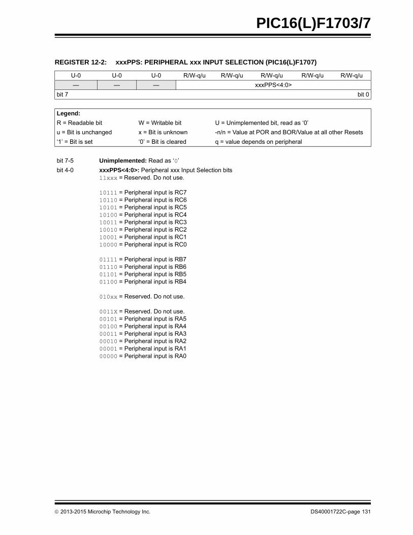
PIC16(L)F1703/7
REGISTER 12-2: xxxPPS: PERIPHERAL xxx INPUT SELECTION (PIC16(L)F1707)
U-0 U-0 U-0 R/W-q/u R/W-q/u R/W-q/u R/W-q/u R/W-q/u
— — — xxxPPS<4:0>
bit 7 bit 0
Legend:
R = Readable bit W = Writable bit U = Unimplemented bit, read as ‘0’
u = Bit is unchanged x = Bit is unknown -n/n = Value at POR and BOR/Value at all other Resets
‘1’ = Bit is set ‘0’ = Bit is cleared q = value depends on peripheral
bit 7-5 Unimplemented: Read as ‘0’
bit 4-0 xxxPPS<4:0>: Peripheral xxx Input Selection bits11xxx = Reserved. Do not use.
10111 = Peripheral input is RC710110 = Peripheral input is RC610101 = Peripheral input is RC510100 = Peripheral input is RC410011 = Peripheral input is RC310010 = Peripheral input is RC210001 = Peripheral input is RC110000 = Peripheral input is RC0
01111 = Peripheral input is RB701110 = Peripheral input is RB601101 = Peripheral input is RB501100 = Peripheral input is RB4
010xx = Reserved. Do not use.
0011X = Reserved. Do not use.00101 = Peripheral input is RA500100 = Peripheral input is RA400011 = Peripheral input is RA300010 = Peripheral input is RA200001 = Peripheral input is RA100000 = Peripheral input is RA0
2013-2015 Microchip Technology Inc. DS40001722C-page 131
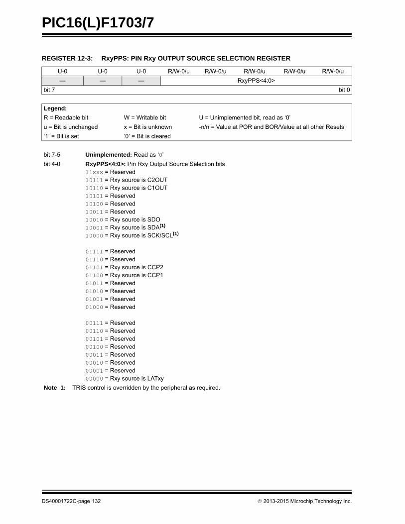
PIC16(L)F1703/7
REGISTER 12-3: RxyPPS: PIN Rxy OUTPUT SOURCE SELECTION REGISTER
U-0 U-0 U-0 R/W-0/u R/W-0/u R/W-0/u R/W-0/u R/W-0/u
— — — RxyPPS<4:0>
bit 7 bit 0
Legend:
R = Readable bit W = Writable bit U = Unimplemented bit, read as ‘0’
u = Bit is unchanged x = Bit is unknown -n/n = Value at POR and BOR/Value at all other Resets
‘1’ = Bit is set ‘0’ = Bit is cleared
bit 7-5 Unimplemented: Read as ‘0’
bit 4-0 RxyPPS<4:0>: Pin Rxy Output Source Selection bits11xxx = Reserved 10111 = Rxy source is C2OUT10110 = Rxy source is C1OUT10101 = Reserved10100 = Reserved10011 = Reserved10010 = Rxy source is SDO10001 = Rxy source is SDA(1)
10000 = Rxy source is SCK/SCL(1)
01111 = Reserved01110 = Reserved01101 = Rxy source is CCP201100 = Rxy source is CCP101011 = Reserved01010 = Reserved01001 = Reserved01000 = Reserved
00111 = Reserved 00110 = Reserved00101 = Reserved00100 = Reserved00011 = Reserved00010 = Reserved00001 = Reserved00000 = Rxy source is LATxy
Note 1: TRIS control is overridden by the peripheral as required.
DS40001722C-page 132 2013-2015 Microchip Technology Inc.
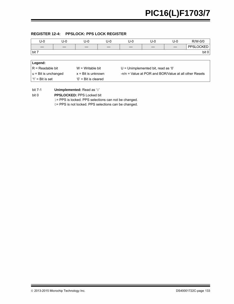
PIC16(L)F1703/7
REGISTER 12-4: PPSLOCK: PPS LOCK REGISTER
U-0 U-0 U-0 U-0 U-0 U-0 U-0 R/W-0/0
— — — — — — — PPSLOCKED
bit 7 bit 0
Legend:
R = Readable bit W = Writable bit U = Unimplemented bit, read as ‘0’
u = Bit is unchanged x = Bit is unknown -n/n = Value at POR and BOR/Value at all other Resets
‘1’ = Bit is set ‘0’ = Bit is cleared
bit 7-1 Unimplemented: Read as ‘0’
bit 0 PPSLOCKED: PPS Locked bit1= PPS is locked. PPS selections can not be changed.0= PPS is not locked. PPS selections can be changed.
2013-2015 Microchip Technology Inc. DS40001722C-page 133
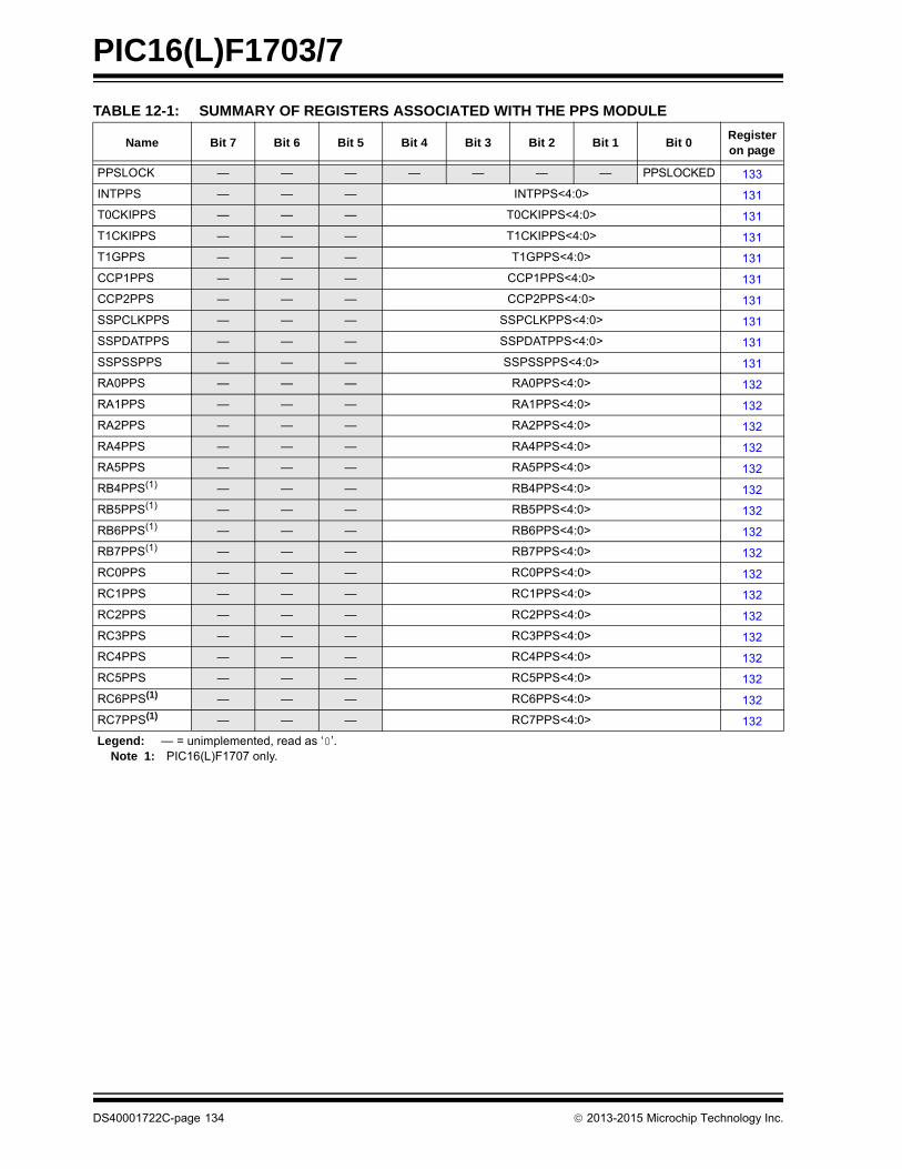
PIC16(L)F1703/7
TABLE 12-1: SUMMARY OF REGISTERS ASSOCIATED WITH THE PPS MODULE
Name Bit 7 Bit 6 Bit 5 Bit 4 Bit 3 Bit 2 Bit 1 Bit 0Register on page
PPSLOCK — — — — — — — PPSLOCKED 133
INTPPS — — — INTPPS<4:0> 131
T0CKIPPS — — — T0CKIPPS<4:0> 131
T1CKIPPS — — — T1CKIPPS<4:0> 131
T1GPPS — — — T1GPPS<4:0> 131
CCP1PPS — — — CCP1PPS<4:0> 131
CCP2PPS — — — CCP2PPS<4:0> 131
SSPCLKPPS — — — SSPCLKPPS<4:0> 131
SSPDATPPS — — — SSPDATPPS<4:0> 131
SSPSSPPS — — — SSPSSPPS<4:0> 131
RA0PPS — — — RA0PPS<4:0> 132
RA1PPS — — — RA1PPS<4:0> 132
RA2PPS — — — RA2PPS<4:0> 132
RA4PPS — — — RA4PPS<4:0> 132
RA5PPS — — — RA5PPS<4:0> 132
RB4PPS(1) — — — RB4PPS<4:0> 132
RB5PPS(1) — — — RB5PPS<4:0> 132
RB6PPS(1) — — — RB6PPS<4:0> 132
RB7PPS(1) — — — RB7PPS<4:0> 132
RC0PPS — — — RC0PPS<4:0> 132
RC1PPS — — — RC1PPS<4:0> 132
RC2PPS — — — RC2PPS<4:0> 132
RC3PPS — — — RC3PPS<4:0> 132
RC4PPS — — — RC4PPS<4:0> 132
RC5PPS — — — RC5PPS<4:0> 132
RC6PPS(1) — — — RC6PPS<4:0> 132
RC7PPS(1) — — — RC7PPS<4:0> 132
Legend: — = unimplemented, read as ‘0’.Note 1: PIC16(L)F1707 only.
DS40001722C-page 134 2013-2015 Microchip Technology Inc.

PIC16(L)F1703/7
13.0 INTERRUPT-ON-CHANGE
All pins on all ports can be configured to operate asInterrupt-On-Change (IOC) pins. An interrupt can begenerated by detecting a signal that has either a risingedge or a falling edge. Any individual pin, or combinationof pins, can be configured to generate an interrupt. Theinterrupt-on-change module has the following features:
• Interrupt-on-Change enable (Master Switch)
• Individual pin configuration
• Rising and falling edge detection
• Individual pin interrupt flags
Figure 13-1 is a block diagram of the IOC module.
13.1 Enabling the Module
To allow individual pins to generate an interrupt, theIOCIE bit of the INTCON register must be set. If theIOCIE bit is disabled, the edge detection on the pin willstill occur, but an interrupt will not be generated.
13.2 Individual Pin Configuration
For each pin, a rising edge detector and a falling edgedetector are present. To enable a pin to detect a risingedge, the associated bit of the IOCxP register is set. Toenable a pin to detect a falling edge, the associated bitof the IOCxN register is set.
A pin can be configured to detect rising and fallingedges simultaneously by setting the associated bits inboth of the IOCxP and IOCxN registers.
13.3 Interrupt Flags
The bits located in the IOCxF registers are status flagsthat correspond to the interrupt-on-change pins of eachport. If an expected edge is detected on an appropriatelyenabled pin, then the status flag for that pin will be set,and an interrupt will be generated if the IOCIE bit is set.The IOCIF bit of the INTCON register reflects the statusof all IOCxF bits.
13.4 Clearing Interrupt Flags
The individual status flags, (IOCxF register bits), can becleared by resetting them to zero. If another edge isdetected during this clearing operation, the associatedstatus flag will be set at the end of the sequence,regardless of the value actually being written.
In order to ensure that no detected edge is lost whileclearing flags, only AND operations masking out knownchanged bits should be performed. The followingsequence is an example of what should be performed.
EXAMPLE 13-1: CLEARING INTERRUPT FLAGS(PORTA EXAMPLE)
13.5 Operation in Sleep
The interrupt-on-change interrupt sequence will wakethe device from Sleep mode, if the IOCIE bit is set.
If an edge is detected while in Sleep mode, the affectedIOCxF register will be updated prior to the first instructionexecuted out of Sleep.
MOVLW 0xffXORWF IOCAF, WANDWF IOCAF, F
2013-2015 Microchip Technology Inc. DS40001722C-page 135
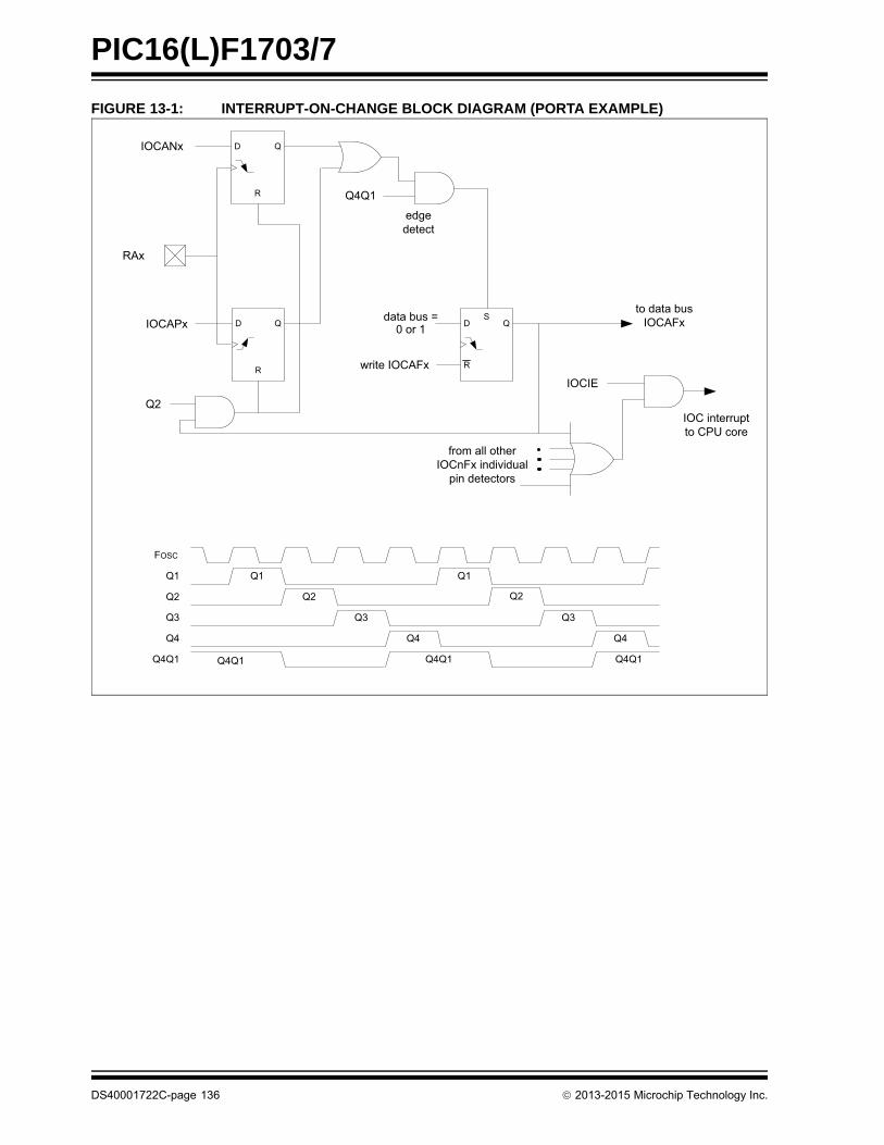
PIC16(L)F1703/7
FIGURE 13-1: INTERRUPT-ON-CHANGE BLOCK DIAGRAM (PORTA EXAMPLE)
IOCANx
IOCAPx
Q2
Q4Q1
data bus =0 or 1
write IOCAFxIOCIE
to data busIOCAFx
edgedetect
IOC interruptto CPU core
from all otherIOCnFx individual
pin detectors
D Q
R
S
D Q
R
D Q
R
RAx
Q1
Q2
Q3
Q4
Q4Q1
Q1
Q2
Q3
Q4
Q1
Q2
Q3
Q4
Q4Q1 Q4Q1Q4Q1
FOSC
DS40001722C-page 136 2013-2015 Microchip Technology Inc.
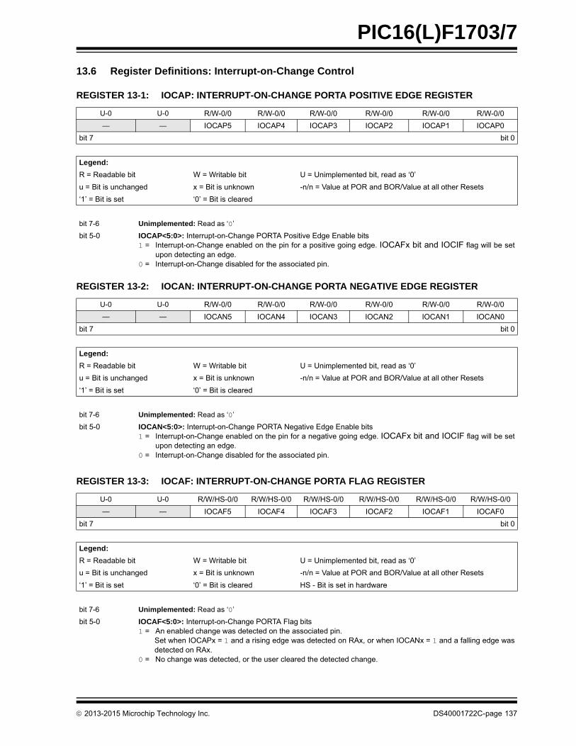
PIC16(L)F1703/7
13.6 Register Definitions: Interrupt-on-Change Control
REGISTER 13-1: IOCAP: INTERRUPT-ON-CHANGE PORTA POSITIVE EDGE REGISTER
U-0 U-0 R/W-0/0 R/W-0/0 R/W-0/0 R/W-0/0 R/W-0/0 R/W-0/0
— — IOCAP5 IOCAP4 IOCAP3 IOCAP2 IOCAP1 IOCAP0
bit 7 bit 0
Legend:
R = Readable bit W = Writable bit U = Unimplemented bit, read as ‘0’
u = Bit is unchanged x = Bit is unknown -n/n = Value at POR and BOR/Value at all other Resets
‘1’ = Bit is set ‘0’ = Bit is cleared
bit 7-6 Unimplemented: Read as ‘0’
bit 5-0 IOCAP<5:0>: Interrupt-on-Change PORTA Positive Edge Enable bits1 = Interrupt-on-Change enabled on the pin for a positive going edge. IOCAFx bit and IOCIF flag will be set
upon detecting an edge.0 = Interrupt-on-Change disabled for the associated pin.
REGISTER 13-2: IOCAN: INTERRUPT-ON-CHANGE PORTA NEGATIVE EDGE REGISTER
U-0 U-0 R/W-0/0 R/W-0/0 R/W-0/0 R/W-0/0 R/W-0/0 R/W-0/0
— — IOCAN5 IOCAN4 IOCAN3 IOCAN2 IOCAN1 IOCAN0
bit 7 bit 0
Legend:
R = Readable bit W = Writable bit U = Unimplemented bit, read as ‘0’
u = Bit is unchanged x = Bit is unknown -n/n = Value at POR and BOR/Value at all other Resets
‘1’ = Bit is set ‘0’ = Bit is cleared
bit 7-6 Unimplemented: Read as ‘0’
bit 5-0 IOCAN<5:0>: Interrupt-on-Change PORTA Negative Edge Enable bits1 = Interrupt-on-Change enabled on the pin for a negative going edge. IOCAFx bit and IOCIF flag will be set
upon detecting an edge.0 = Interrupt-on-Change disabled for the associated pin.
REGISTER 13-3: IOCAF: INTERRUPT-ON-CHANGE PORTA FLAG REGISTER
U-0 U-0 R/W/HS-0/0 R/W/HS-0/0 R/W/HS-0/0 R/W/HS-0/0 R/W/HS-0/0 R/W/HS-0/0
— — IOCAF5 IOCAF4 IOCAF3 IOCAF2 IOCAF1 IOCAF0
bit 7 bit 0
Legend:
R = Readable bit W = Writable bit U = Unimplemented bit, read as ‘0’
u = Bit is unchanged x = Bit is unknown -n/n = Value at POR and BOR/Value at all other Resets
‘1’ = Bit is set ‘0’ = Bit is cleared HS - Bit is set in hardware
bit 7-6 Unimplemented: Read as ‘0’
bit 5-0 IOCAF<5:0>: Interrupt-on-Change PORTA Flag bits1 = An enabled change was detected on the associated pin.
Set when IOCAPx = 1 and a rising edge was detected on RAx, or when IOCANx = 1 and a falling edge wasdetected on RAx.
0 = No change was detected, or the user cleared the detected change.
2013-2015 Microchip Technology Inc. DS40001722C-page 137
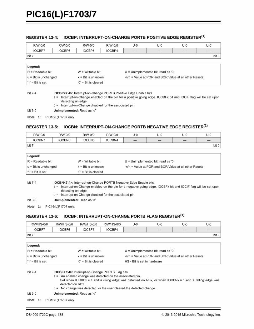
PIC16(L)F1703/7
REGISTER 13-4: IOCBP: INTERRUPT-ON-CHANGE PORTB POSITIVE EDGE REGISTER(1)
R/W-0/0 R/W-0/0 R/W-0/0 R/W-0/0 U-0 U-0 U-0 U-0
IOCBP7 IOCBP6 IOCBP5 IOCBP4 — — — —
bit 7 bit 0
Legend:
R = Readable bit W = Writable bit U = Unimplemented bit, read as ‘0’
u = Bit is unchanged x = Bit is unknown -n/n = Value at POR and BOR/Value at all other Resets
‘1’ = Bit is set ‘0’ = Bit is cleared
bit 7-4 IOCBP<7:4>: Interrupt-on-Change PORTB Positive Edge Enable bits1 = Interrupt-on-Change enabled on the pin for a positive going edge. IOCBFx bit and IOCIF flag will be set upon
detecting an edge.0 = Interrupt-on-Change disabled for the associated pin.
bit 3-0 Unimplemented: Read as ‘0’
Note 1: PIC16(L)F1707 only.
REGISTER 13-5: IOCBN: INTERRUPT-ON-CHANGE PORTB NEGATIVE EDGE REGISTER(1)
R/W-0/0 R/W-0/0 R/W-0/0 R/W-0/0 U-0 U-0 U-0 U-0
IOCBN7 IOCBN6 IOCBN5 IOCBN4 — — — —
bit 7 bit 0
Legend:
R = Readable bit W = Writable bit U = Unimplemented bit, read as ‘0’
u = Bit is unchanged x = Bit is unknown -n/n = Value at POR and BOR/Value at all other Resets
‘1’ = Bit is set ‘0’ = Bit is cleared
bit 7-4 IOCBN<7:4>: Interrupt-on-Change PORTB Negative Edge Enable bits1 = Interrupt-on-Change enabled on the pin for a negative going edge. IOCBFx bit and IOCIF flag will be set upon
detecting an edge.0 = Interrupt-on-Change disabled for the associated pin.
bit 3-0 Unimplemented: Read as ‘0’
Note 1: PIC16(L)F1707 only.
REGISTER 13-6: IOCBF: INTERRUPT-ON-CHANGE PORTB FLAG REGISTER(1)
R/W/HS-0/0 R/W/HS-0/0 R/W/HS-0/0 R/W/HS-0/0 U-0 U-0 U-0 U-0
IOCBF7 IOCBF6 IOCBF5 IOCBF4 — — — —
bit 7 bit 0
Legend:
R = Readable bit W = Writable bit U = Unimplemented bit, read as ‘0’
u = Bit is unchanged x = Bit is unknown -n/n = Value at POR and BOR/Value at all other Resets
‘1’ = Bit is set ‘0’ = Bit is cleared HS - Bit is set in hardware
bit 7-4 IOCBF<7:4>: Interrupt-on-Change PORTB Flag bits1 = An enabled change was detected on the associated pin.
Set when IOCBPx = 1 and a rising edge was detected on RBx, or when IOCBNx = 1 and a falling edge wasdetected on RBx.
0 = No change was detected, or the user cleared the detected change.
bit 3-0 Unimplemented: Read as ‘0’
Note 1: PIC16(L)F1707 only.
DS40001722C-page 138 2013-2015 Microchip Technology Inc.
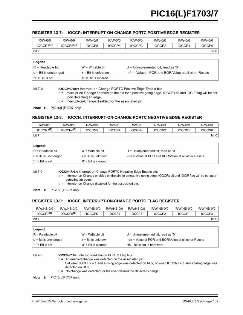
PIC16(L)F1703/7
REGISTER 13-7: IOCCP: INTERRUPT-ON-CHANGE PORTC POSITIVE EDGE REGISTER
R/W-0/0 R/W-0/0 R/W-0/0 R/W-0/0 R/W-0/0 R/W-0/0 R/W-0/0 R/W-0/0
IOCCP7(1) IOCCP6(1) IOCCP5 IOCCP4 IOCCP3 IOCCP2 IOCCP1 IOCCP0
bit 7 bit 0
Legend:
R = Readable bit W = Writable bit U = Unimplemented bit, read as ‘0’
u = Bit is unchanged x = Bit is unknown -n/n = Value at POR and BOR/Value at all other Resets
‘1’ = Bit is set ‘0’ = Bit is cleared
bit 7-0 IOCCP<7:0>: Interrupt-on-Change PORTC Positive Edge Enable bits1 = Interrupt-on-Change enabled on the pin for a positive going edge. IOCCFx bit and IOCIF flag will be set
upon detecting an edge.0 = Interrupt-on-Change disabled for the associated pin.
Note 1: PIC16(L)F1707 only.
REGISTER 13-8: IOCCN: INTERRUPT-ON-CHANGE PORTC NEGATIVE EDGE REGISTER
R/W-0/0 R/W-0/0 R/W-0/0 R/W-0/0 R/W-0/0 R/W-0/0 R/W-0/0 R/W-0/0
IOCCN7(1) IOCCN6(1) IOCCN5 IOCCN4 IOCCN3 IOCCN2 IOCCN1 IOCCN0
bit 7 bit 0
Legend:
R = Readable bit W = Writable bit U = Unimplemented bit, read as ‘0’
u = Bit is unchanged x = Bit is unknown -n/n = Value at POR and BOR/Value at all other Resets
‘1’ = Bit is set ‘0’ = Bit is cleared
bit 7-0 IOCCN<7:0>: Interrupt-on-Change PORTC Negative Edge Enable bits1 = Interrupt-on-Change enabled on the pin for a negative going edge. IOCCFx bit and IOCIF flag will be set upon
detecting an edge.0 = Interrupt-on-Change disabled for the associated pin.
Note 1: PIC16(L)F1707 only.
REGISTER 13-9: IOCCF: INTERRUPT-ON-CHANGE PORTC FLAG REGISTER
R/W/HS-0/0 R/W/HS-0/0 R/W/HS-0/0 R/W/HS-0/0 R/W/HS-0/0 R/W/HS-0/0 R/W/HS-0/0 R/W/HS-0/0
IOCCF7(1) IOCCF6(1) IOCCF5 IOCCF4 IOCCF3 IOCCF2 IOCCF1 IOCCF0
bit 7 bit 0
Legend:
R = Readable bit W = Writable bit U = Unimplemented bit, read as ‘0’
u = Bit is unchanged x = Bit is unknown -n/n = Value at POR and BOR/Value at all other Resets
‘1’ = Bit is set ‘0’ = Bit is cleared HS - Bit is set in hardware
bit 7-0 IOCCF<7:0>: Interrupt-on-Change PORTC Flag bits1 = An enabled change was detected on the associated pin.
Set when IOCCPx = 1 and a rising edge was detected on RCx, or when IOCCNx = 1 and a falling edge wasdetected on RCx.
0 = No change was detected, or the user cleared the detected change.
Note 1: PIC16(L)F1707 only.
2013-2015 Microchip Technology Inc. DS40001722C-page 139
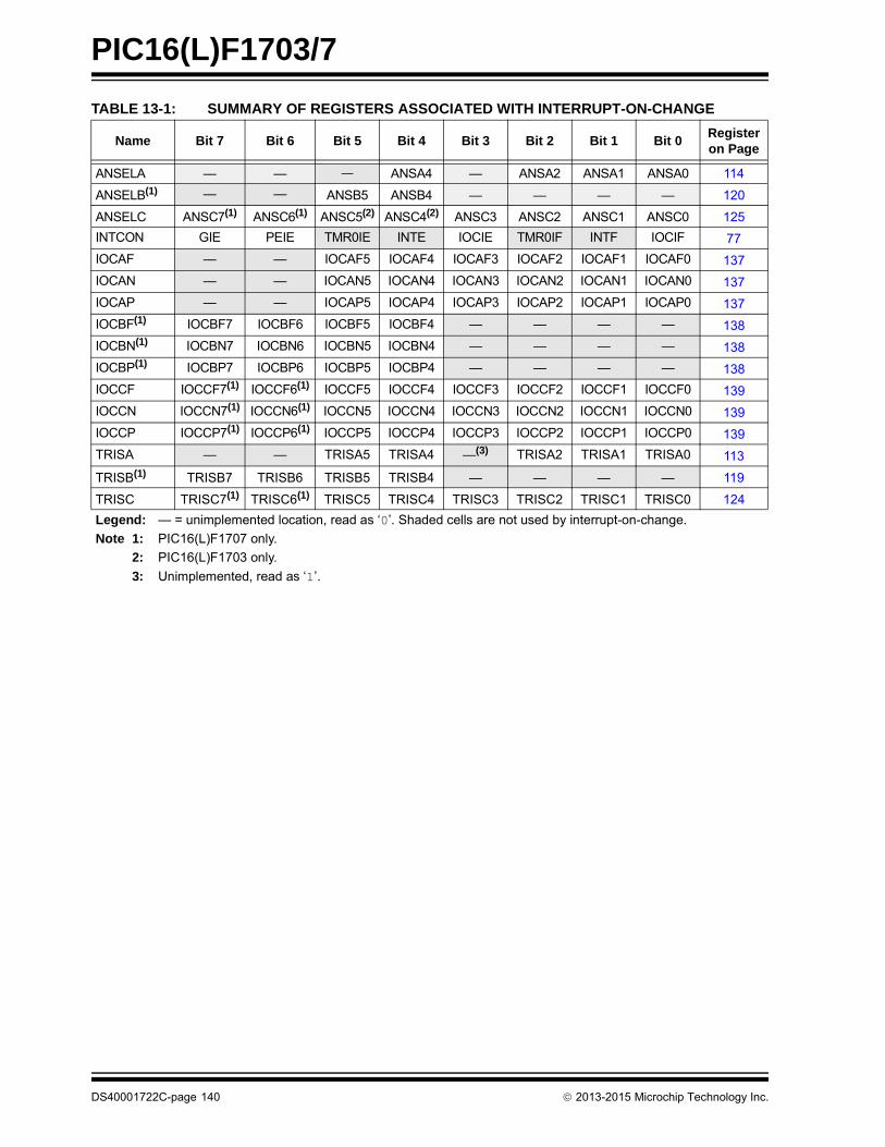
PIC16(L)F1703/7
TABLE 13-1: SUMMARY OF REGISTERS ASSOCIATED WITH INTERRUPT-ON-CHANGE
Name Bit 7 Bit 6 Bit 5 Bit 4 Bit 3 Bit 2 Bit 1 Bit 0Register on Page
ANSELA — — — ANSA4 — ANSA2 ANSA1 ANSA0 114
ANSELB(1) — — ANSB5 ANSB4 — — — — 120
ANSELC ANSC7(1) ANSC6(1) ANSC5(2) ANSC4(2) ANSC3 ANSC2 ANSC1 ANSC0 125
INTCON GIE PEIE TMR0IE INTE IOCIE TMR0IF INTF IOCIF 77
IOCAF — — IOCAF5 IOCAF4 IOCAF3 IOCAF2 IOCAF1 IOCAF0 137
IOCAN — — IOCAN5 IOCAN4 IOCAN3 IOCAN2 IOCAN1 IOCAN0 137
IOCAP — — IOCAP5 IOCAP4 IOCAP3 IOCAP2 IOCAP1 IOCAP0 137
IOCBF(1) IOCBF7 IOCBF6 IOCBF5 IOCBF4 — — — — 138
IOCBN(1) IOCBN7 IOCBN6 IOCBN5 IOCBN4 — — — — 138
IOCBP(1) IOCBP7 IOCBP6 IOCBP5 IOCBP4 — — — — 138
IOCCF IOCCF7(1) IOCCF6(1) IOCCF5 IOCCF4 IOCCF3 IOCCF2 IOCCF1 IOCCF0 139
IOCCN IOCCN7(1) IOCCN6(1) IOCCN5 IOCCN4 IOCCN3 IOCCN2 IOCCN1 IOCCN0 139
IOCCP IOCCP7(1) IOCCP6(1) IOCCP5 IOCCP4 IOCCP3 IOCCP2 IOCCP1 IOCCP0 139
TRISA — — TRISA5 TRISA4 —(3) TRISA2 TRISA1 TRISA0 113
TRISB(1) TRISB7 TRISB6 TRISB5 TRISB4 — — — — 119
TRISC TRISC7(1) TRISC6(1) TRISC5 TRISC4 TRISC3 TRISC2 TRISC1 TRISC0 124
Legend: — = unimplemented location, read as ‘0’. Shaded cells are not used by interrupt-on-change.
Note 1: PIC16(L)F1707 only.
2: PIC16(L)F1703 only.
3: Unimplemented, read as ‘1’.
DS40001722C-page 140 2013-2015 Microchip Technology Inc.
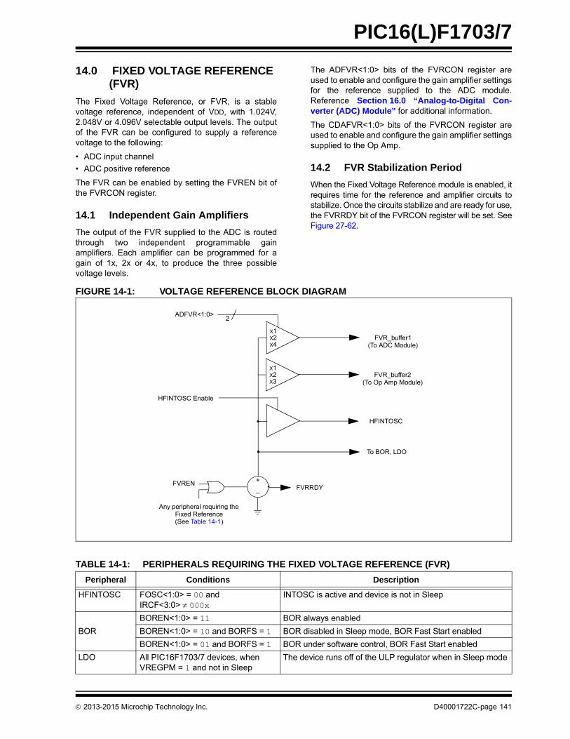
PIC16(L)F1703/7
14.0 FIXED VOLTAGE REFERENCE (FVR)
The Fixed Voltage Reference, or FVR, is a stablevoltage reference, independent of VDD, with 1.024V,2.048V or 4.096V selectable output levels. The outputof the FVR can be configured to supply a referencevoltage to the following:
• ADC input channel
• ADC positive reference
The FVR can be enabled by setting the FVREN bit ofthe FVRCON register.
14.1 Independent Gain Amplifiers
The output of the FVR supplied to the ADC is routedthrough two independent programmable gainamplifiers. Each amplifier can be programmed for again of 1x, 2x or 4x, to produce the three possiblevoltage levels.
The ADFVR<1:0> bits of the FVRCON register areused to enable and configure the gain amplifier settingsfor the reference supplied to the ADC module.Reference Section 16.0 “Analog-to-Digital Con-verter (ADC) Module” for additional information.
The CDAFVR<1:0> bits of the FVRCON register areused to enable and configure the gain amplifier settingssupplied to the Op Amp.
14.2 FVR Stabilization Period
When the Fixed Voltage Reference module is enabled, itrequires time for the reference and amplifier circuits tostabilize. Once the circuits stabilize and are ready for use,the FVRRDY bit of the FVRCON register will be set. SeeFigure 27-62.
FIGURE 14-1: VOLTAGE REFERENCE BLOCK DIAGRAM
ADFVR<1:0>
X1X2X4
2
FVR_buffer1(To ADC Module)
+
_FVREN
FVRRDY
Any peripheral requiring the Fixed Reference(See Table 14-1)
To BOR, LDO
HFINTOSC Enable
HFINTOSC
X1X2X3
FVR_buffer2(To Op Amp Module)
TABLE 14-1: PERIPHERALS REQUIRING THE FIXED VOLTAGE REFERENCE (FVR)
Peripheral Conditions Description
HFINTOSC FOSC<1:0> = 00 and IRCF<3:0> 000x
INTOSC is active and device is not in Sleep
BOR
BOREN<1:0> = 11 BOR always enabled
BOREN<1:0> = 10 and BORFS = 1 BOR disabled in Sleep mode, BOR Fast Start enabled
BOREN<1:0> = 01 and BORFS = 1 BOR under software control, BOR Fast Start enabled
LDO All PIC16F1703/7 devices, when VREGPM = 1 and not in Sleep
The device runs off of the ULP regulator when in Sleep mode
2013-2015 Microchip Technology Inc. D40001722C-page 141
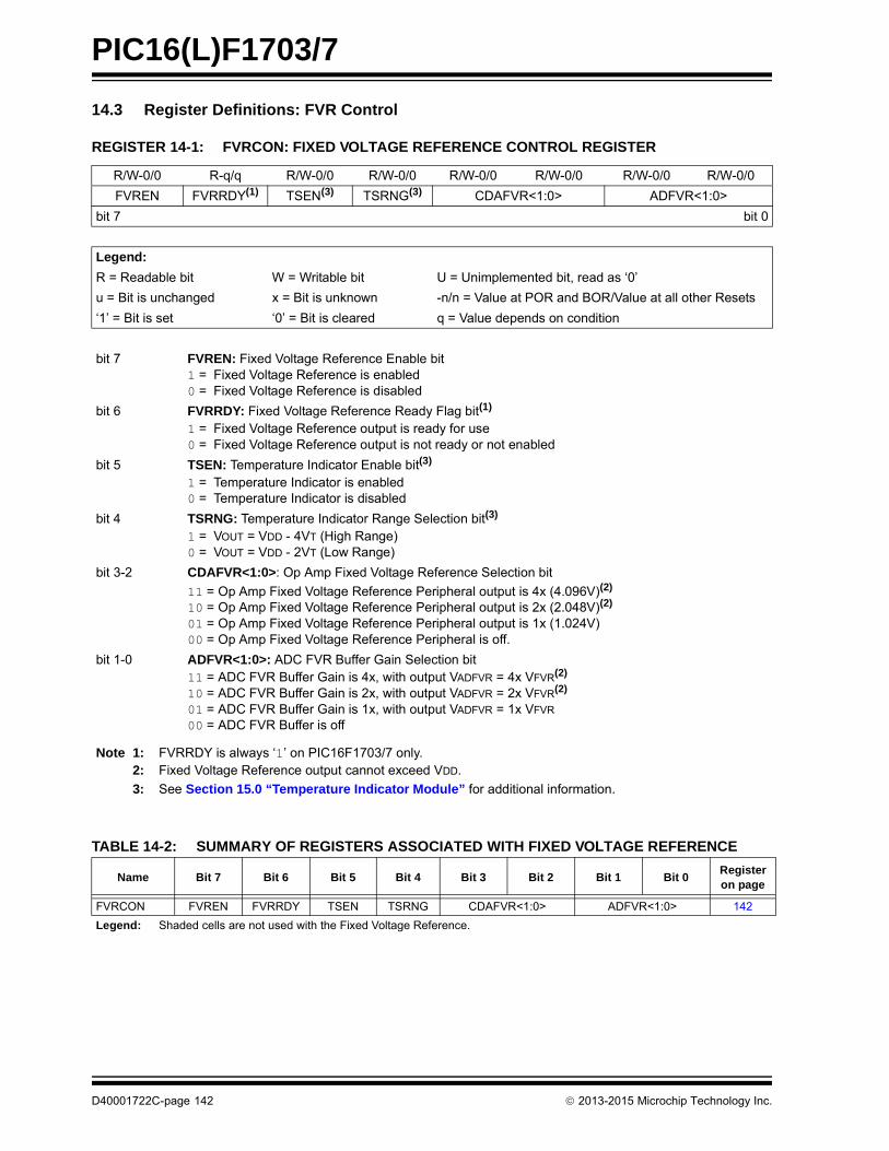
PIC16(L)F1703/7
14.3 Register Definitions: FVR Control
TABLE 14-2: SUMMARY OF REGISTERS ASSOCIATED WITH FIXED VOLTAGE REFERENCE
REGISTER 14-1: FVRCON: FIXED VOLTAGE REFERENCE CONTROL REGISTER
R/W-0/0 R-q/q R/W-0/0 R/W-0/0 R/W-0/0 R/W-0/0 R/W-0/0 R/W-0/0
FVREN FVRRDY(1) TSEN(3) TSRNG(3) CDAFVR<1:0> ADFVR<1:0>
bit 7 bit 0
Legend:
R = Readable bit W = Writable bit U = Unimplemented bit, read as ‘0’
u = Bit is unchanged x = Bit is unknown -n/n = Value at POR and BOR/Value at all other Resets
‘1’ = Bit is set ‘0’ = Bit is cleared q = Value depends on condition
bit 7 FVREN: Fixed Voltage Reference Enable bit1 = Fixed Voltage Reference is enabled0 = Fixed Voltage Reference is disabled
bit 6 FVRRDY: Fixed Voltage Reference Ready Flag bit(1)
1 = Fixed Voltage Reference output is ready for use0 = Fixed Voltage Reference output is not ready or not enabled
bit 5 TSEN: Temperature Indicator Enable bit(3)
1 = Temperature Indicator is enabled0 = Temperature Indicator is disabled
bit 4 TSRNG: Temperature Indicator Range Selection bit(3)
1 = VOUT = VDD - 4VT (High Range)0 = VOUT = VDD - 2VT (Low Range)
bit 3-2 CDAFVR<1:0>: Op Amp Fixed Voltage Reference Selection bit
11 = Op Amp Fixed Voltage Reference Peripheral output is 4x (4.096V)(2)
10 = Op Amp Fixed Voltage Reference Peripheral output is 2x (2.048V)(2)
01 = Op Amp Fixed Voltage Reference Peripheral output is 1x (1.024V)00 = Op Amp Fixed Voltage Reference Peripheral is off.
bit 1-0 ADFVR<1:0>: ADC FVR Buffer Gain Selection bit11 = ADC FVR Buffer Gain is 4x, with output VADFVR = 4x VFVR(2)
10 = ADC FVR Buffer Gain is 2x, with output VADFVR = 2x VFVR(2)
01 = ADC FVR Buffer Gain is 1x, with output VADFVR = 1x VFVR
00 = ADC FVR Buffer is off
Note 1: FVRRDY is always ‘1’ on PIC16F1703/7 only.2: Fixed Voltage Reference output cannot exceed VDD.
3: See Section 15.0 “Temperature Indicator Module” for additional information.
Name Bit 7 Bit 6 Bit 5 Bit 4 Bit 3 Bit 2 Bit 1 Bit 0Register on page
FVRCON FVREN FVRRDY TSEN TSRNG CDAFVR<1:0> ADFVR<1:0> 142
Legend: Shaded cells are not used with the Fixed Voltage Reference.
D40001722C-page 142 2013-2015 Microchip Technology Inc.
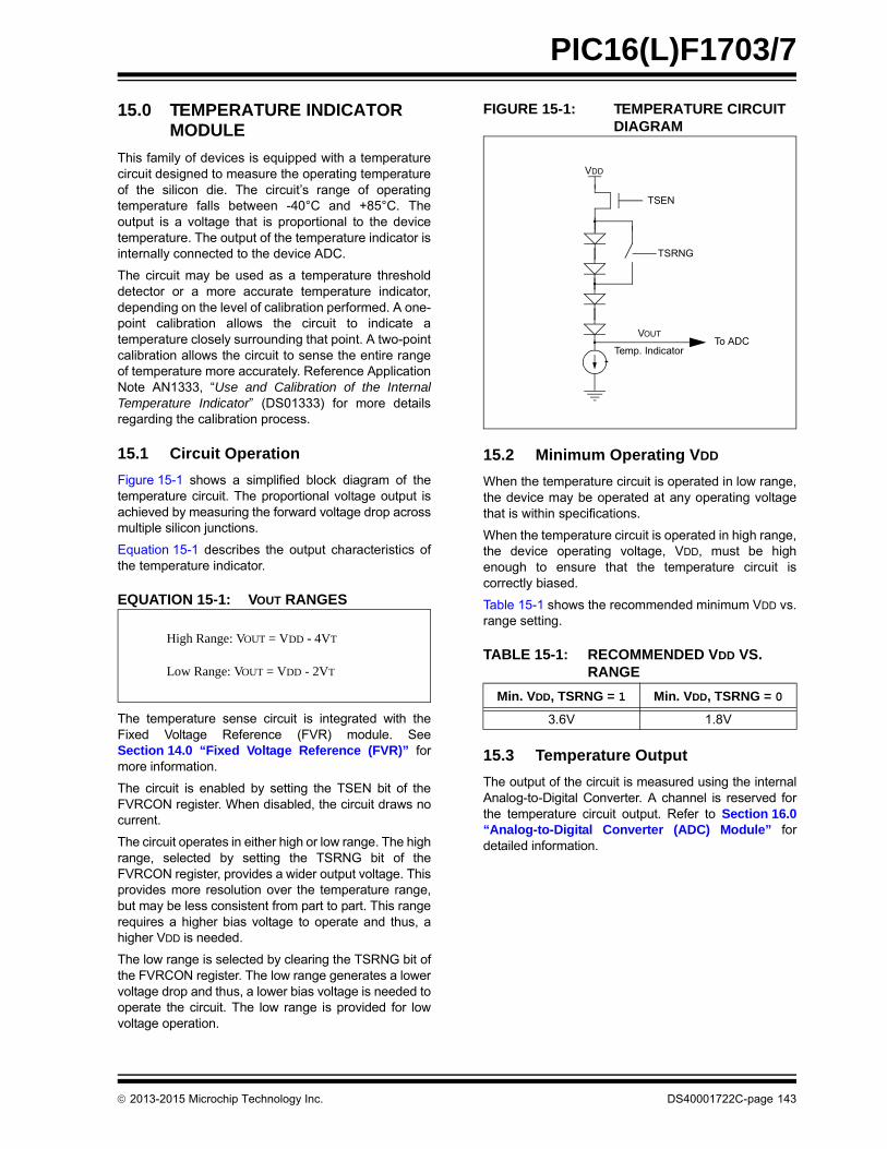
PIC16(L)F1703/7
15.0 TEMPERATURE INDICATOR MODULE
This family of devices is equipped with a temperaturecircuit designed to measure the operating temperatureof the silicon die. The circuit’s range of operatingtemperature falls between -40°C and +85°C. Theoutput is a voltage that is proportional to the devicetemperature. The output of the temperature indicator isinternally connected to the device ADC.
The circuit may be used as a temperature thresholddetector or a more accurate temperature indicator,depending on the level of calibration performed. A one-point calibration allows the circuit to indicate atemperature closely surrounding that point. A two-pointcalibration allows the circuit to sense the entire rangeof temperature more accurately. Reference ApplicationNote AN1333, “Use and Calibration of the InternalTemperature Indicator” (DS01333) for more detailsregarding the calibration process.
15.1 Circuit Operation
Figure 15-1 shows a simplified block diagram of thetemperature circuit. The proportional voltage output isachieved by measuring the forward voltage drop acrossmultiple silicon junctions.
Equation 15-1 describes the output characteristics ofthe temperature indicator.
EQUATION 15-1: VOUT RANGES
The temperature sense circuit is integrated with theFixed Voltage Reference (FVR) module. SeeSection 14.0 “Fixed Voltage Reference (FVR)” formore information.
The circuit is enabled by setting the TSEN bit of theFVRCON register. When disabled, the circuit draws nocurrent.
The circuit operates in either high or low range. The highrange, selected by setting the TSRNG bit of theFVRCON register, provides a wider output voltage. Thisprovides more resolution over the temperature range,but may be less consistent from part to part. This rangerequires a higher bias voltage to operate and thus, ahigher VDD is needed.
The low range is selected by clearing the TSRNG bit ofthe FVRCON register. The low range generates a lowervoltage drop and thus, a lower bias voltage is needed tooperate the circuit. The low range is provided for lowvoltage operation.
FIGURE 15-1: TEMPERATURE CIRCUIT DIAGRAM
15.2 Minimum Operating VDD
When the temperature circuit is operated in low range,the device may be operated at any operating voltagethat is within specifications.
When the temperature circuit is operated in high range,the device operating voltage, VDD, must be highenough to ensure that the temperature circuit iscorrectly biased.
Table 15-1 shows the recommended minimum VDD vs.range setting.
TABLE 15-1: RECOMMENDED VDD VS. RANGE
15.3 Temperature Output
The output of the circuit is measured using the internalAnalog-to-Digital Converter. A channel is reserved forthe temperature circuit output. Refer to Section 16.0“Analog-to-Digital Converter (ADC) Module” fordetailed information.
High Range: VOUT = VDD - 4VT
Low Range: VOUT = VDD - 2VT
Min. VDD, TSRNG = 1 Min. VDD, TSRNG = 0
3.6V 1.8V
TSEN
TSRNG
VDD
VOUTTo ADC
Temp. Indicator
2013-2015 Microchip Technology Inc. DS40001722C-page 143

PIC16(L)F1703/7
15.4 ADC Acquisition Time
To ensure accurate temperature measurements, theuser must wait at least 200 s after the ADC inputmultiplexer is connected to the temperature indicatoroutput before the conversion is performed. In addition,the user must wait 200 s between sequentialconversions of the temperature indicator output.
TABLE 15-2: SUMMARY OF REGISTERS ASSOCIATED WITH THE TEMPERATURE INDICATOR
Name Bit 7 Bit 6 Bit 5 Bit 4 Bit 3 Bit 2 Bit 1 Bit 0Register on page
FVRCON FVREN FVRRDY TSEN TSRNG CDAFVR<1:0> ADFVR<1:0> 142
Legend: Shaded cells are unused by the temperature indicator module.
DS40001722C-page 144 2013-2015 Microchip Technology Inc.
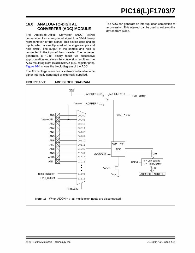
PIC16(L)F1703/7
16.0 ANALOG-TO-DIGITAL CONVERTER (ADC) MODULE
The Analog-to-Digital Converter (ADC) allowsconversion of an analog input signal to a 10-bit binaryrepresentation of that signal. This device uses analoginputs, which are multiplexed into a single sample andhold circuit. The output of the sample and hold isconnected to the input of the converter. The convertergenerates a 10-bit binary result via successiveapproximation and stores the conversion result into theADC result registers (ADRESH:ADRESL register pair).Figure 16-1 shows the block diagram of the ADC.
The ADC voltage reference is software selectable to beeither internally generated or externally supplied.
The ADC can generate an interrupt upon completion ofa conversion. This interrupt can be used to wake-up thedevice from Sleep.
FIGURE 16-1: ADC BLOCK DIAGRAM
VDD
VREF+ ADPREF = 10
ADPREF = 00
FVR_Buffer1
Note 1: When ADON = 0, all multiplexer inputs are disconnected.
ADON
GO/DONE
VSS
ADC
00000
00001
00010
00011
00100
00101
00111
00110
01000
01001
01010
01011
CHS<4:0>
AN0
VREF+/AN1
AN2
AN4
AN5
AN6
AN7
AN3
AN8
AN9
AN10
AN11
11111
ADRESH ADRESL
10
16
ADFM0 = Left Justify1 = Right Justify
Temp Indicator 11101
VREF- = VSS
Ref+ Ref-
ADPREF = 11FVR_Buffer1
2013-2015 Microchip Technology Inc. DS40001722C-page 145
PIC16(L)F1703/7
16.1 ADC Configuration
When configuring and using the ADC the followingfunctions must be considered:
• Port configuration
• Channel selection
• ADC voltage reference selection
• ADC conversion clock source
• Interrupt control
• Result formatting
16.1.1 PORT CONFIGURATION
The ADC can be used to convert both analog anddigital signals. When converting analog signals, the I/Opin should be configured for analog by setting theassociated TRIS and ANSEL bits. Refer toSection 11.0 “I/O Ports” for more information.
16.1.2 CHANNEL SELECTION
There are up to 17 channel selections available:
• AN<13:8, 4:0> pins (PIC16(L)F1703 only)
• AN<21,13:0> pins (PIC16(L)F1707 only)
• Temperature Indicator
• FVR_buffer1
The CHS bits of the ADCON0 register (Register 16-1)determine which channel is connected to the sampleand hold circuit.
When changing channels, a delay is required beforestarting the next conversion. Refer to Section 16.2“ADC Operation” for more information.
16.1.3 ADC VOLTAGE REFERENCE
The ADPREF bits of the ADCON1 register providescontrol of the positive voltage reference. The positivevoltage reference can be:
• VREF+ pin
• VDD
• FVR 2.048V
• FVR 4.096V (Not available on LF devices)
• VSS
See Section 16.0 “Analog-to-Digital Converter(ADC) Module” for more details on the Fixed VoltageReference.
16.1.4 CONVERSION CLOCK
The source of the conversion clock is software select-able via the ADCS bits of the ADCON1 register. Thereare seven possible clock options:
• FOSC/2
• FOSC/4
• FOSC/8
• FOSC/16
• FOSC/32
• FOSC/64
• FRC (internal RC oscillator)
The time to complete one bit conversion is defined asTAD. One full 10-bit conversion requires 11.5 TAD peri-ods as shown in Figure 16-2.
For correct conversion, the appropriate TAD specificationmust be met. Refer to Table 26-15 for more information.Table 16-1 gives examples of appropriate ADC clockselections.
Note: Analog voltages on any pin that is definedas a digital input may cause the input buf-fer to conduct excess current. Note: Unless using the FRC, any changes in the
system clock frequency will change theADC clock frequency, which mayadversely affect the ADC result.
DS40001722C-page 146 2013-2015 Microchip Technology Inc.
PIC16(L)F1703/7
TABLE 16-1: ADC CLOCK PERIOD (TAD) VS. DEVICE OPERATING FREQUENCIES
FIGURE 16-2: ANALOG-TO-DIGITAL CONVERSION TAD CYCLES
ADC Clock Period (TAD) Device Frequency (FOSC)
ADCClock Source
ADCS<2:0> 32 MHz 20 MHz 16 MHz 8 MHz 4 MHz 1 MHz
FOSC/2 000 62.5ns(2) 100 ns(2) 125 ns(2) 250 ns(2) 500 ns(2) 2.0 s
FOSC/4 100 125 ns(2) 200 ns(2) 250 ns(2) 500 ns(2) 1.0 s 4.0 s
FOSC/8 001 0.5 s(2) 400 ns(2) 0.5 s(2) 1.0 s 2.0 s 8.0 s(3)
FOSC/16 101 800 ns 800 ns 1.0 s 2.0 s 4.0 s 16.0 s(3)
FOSC/32 010 1.0 s 1.6 s 2.0 s 4.0 s 8.0 s(3) 32.0 s(2)
FOSC/64 110 2.0 s 3.2 s 4.0 s 8.0 s(3) 16.0 s(2) 64.0 s(2)
FRC x11 1.0-6.0 s(1,4) 1.0-6.0 s(1,4) 1.0-6.0 s(1,4) 1.0-6.0 s(1,4) 1.0-6.0 s(1,4) 1.0-6.0 s(1,4)
Legend: Shaded cells are outside of recommended range.Note 1: See TAD parameter for FRC source typical TAD value.
2: These values violate the required TAD time.3: Outside the recommended TAD time.4: The ADC clock period (TAD) and total ADC conversion time can be minimized when the ADC clock is derived from the
system clock FOSC. However, the FRC oscillator source must be used when conversions are to be performed with the device in Sleep mode.
TAD1 TAD2 TAD3 TAD4 TAD5 TAD6 TAD7 TAD8 TAD9 TAD10 TAD11
Set GO bit
Conversion Starts
Holding capacitor disconnected from analog input (THCD).
On the following cycle:
ADRESH:ADRESL is loaded,GO bit is cleared,
ADIF bit is set,holding capacitor is reconnected to analog input.
b9 b8 b7 b6 b5 b4 b3 b2 b1 b0
Enable ADC (ADON bit)and
Select channel (ACS bits)
THCD
TACQ
2013-2015 Microchip Technology Inc. DS40001722C-page 147
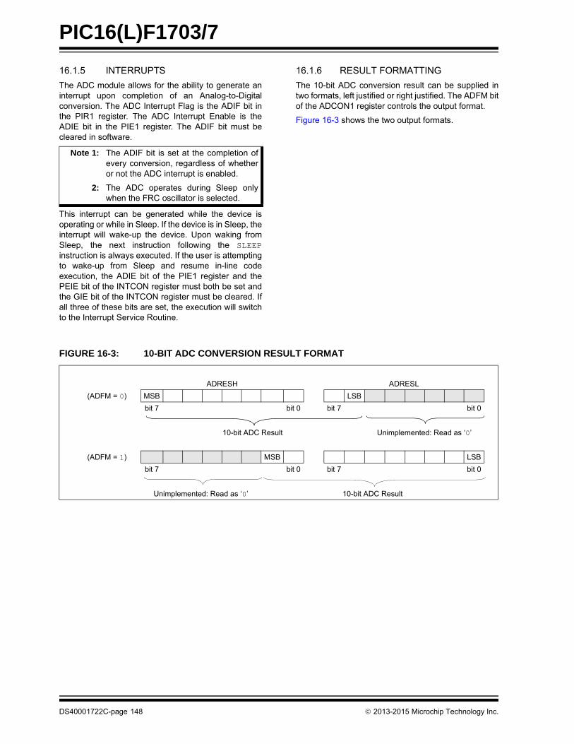
PIC16(L)F1703/7
16.1.5 INTERRUPTS
The ADC module allows for the ability to generate aninterrupt upon completion of an Analog-to-Digitalconversion. The ADC Interrupt Flag is the ADIF bit inthe PIR1 register. The ADC Interrupt Enable is theADIE bit in the PIE1 register. The ADIF bit must becleared in software.
This interrupt can be generated while the device isoperating or while in Sleep. If the device is in Sleep, theinterrupt will wake-up the device. Upon waking fromSleep, the next instruction following the SLEEPinstruction is always executed. If the user is attemptingto wake-up from Sleep and resume in-line codeexecution, the ADIE bit of the PIE1 register and thePEIE bit of the INTCON register must both be set andthe GIE bit of the INTCON register must be cleared. Ifall three of these bits are set, the execution will switchto the Interrupt Service Routine.
16.1.6 RESULT FORMATTING
The 10-bit ADC conversion result can be supplied intwo formats, left justified or right justified. The ADFM bitof the ADCON1 register controls the output format.
Figure 16-3 shows the two output formats.
FIGURE 16-3: 10-BIT ADC CONVERSION RESULT FORMAT
Note 1: The ADIF bit is set at the completion ofevery conversion, regardless of whetheror not the ADC interrupt is enabled.
2: The ADC operates during Sleep onlywhen the FRC oscillator is selected.
ADRESH ADRESL
(ADFM = 0) MSB LSB
bit 7 bit 0 bit 7 bit 0
10-bit ADC Result Unimplemented: Read as ‘0’
(ADFM = 1) MSB LSB
bit 7 bit 0 bit 7 bit 0
Unimplemented: Read as ‘0’ 10-bit ADC Result
DS40001722C-page 148 2013-2015 Microchip Technology Inc.

PIC16(L)F1703/7
16.2 ADC Operation
16.2.1 STARTING A CONVERSION
To enable the ADC module, the ADON bit of theADCON0 register must be set to a ‘1’. Setting theGO/DONE bit of the ADCON0 register to a ‘1’ will startthe Analog-to-Digital conversion.
16.2.2 COMPLETION OF A CONVERSION
When the conversion is complete, the ADC module will:
• Clear the GO/DONE bit
• Set the ADIF Interrupt Flag bit
• Update the ADRESH and ADRESL registers with new conversion result
16.2.3 TERMINATING A CONVERSION
If a conversion must be terminated before completion,the GO/DONE bit can be cleared in software. TheADRESH and ADRESL registers will be updated withthe partially complete Analog-to-Digital conversionsample. Incomplete bits will match the last bitconverted.
16.2.4 ADC OPERATION DURING SLEEP
The ADC module can operate during Sleep. Thisrequires the ADC clock source to be set to the FRCoption. When the FRC oscillator source is selected, theADC waits one additional instruction before starting theconversion. This allows the SLEEP instruction to beexecuted, which can reduce system noise during theconversion. If the ADC interrupt is enabled, the devicewill wake-up from Sleep when the conversioncompletes. If the ADC interrupt is disabled, the ADCmodule is turned off after the conversion completes,although the ADON bit remains set.
When the ADC clock source is something other thanFRC, a SLEEP instruction causes the present conver-sion to be aborted and the ADC module is turned off,although the ADON bit remains set.
16.2.5 AUTO-CONVERSION TRIGGER
The Auto-conversion Trigger allows periodic ADC mea-surements without software intervention. When a risingedge of the selected source occurs, the GO/DONE bitis set by hardware.
The Auto-conversion Trigger source is selected withthe TRIGSEL<3:0> bits of the ADCON2 register.
Using the Auto-conversion Trigger does not assureproper ADC timing. It is the user’s responsibility toensure that the ADC timing requirements are met.
See Table 16-2 for auto-conversion sources.
Note: The GO/DONE bit should not be set in thesame instruction that turns on the ADC.Refer to Section 16.2.6 “ADC Conver-sion Procedure”.
Note: A device Reset forces all registers to theirReset state. Thus, the ADC module isturned off and any pending conversion isterminated.
TABLE 16-2: AUTO-CONVERSION SOURCES
Source Peripheral Signal Name
CCP1
CCP2
Timer0 T0_overflow
Timer1 T1_overflow
Timer2 T2_match
2013-2015 Microchip Technology Inc. DS40001722C-page 149
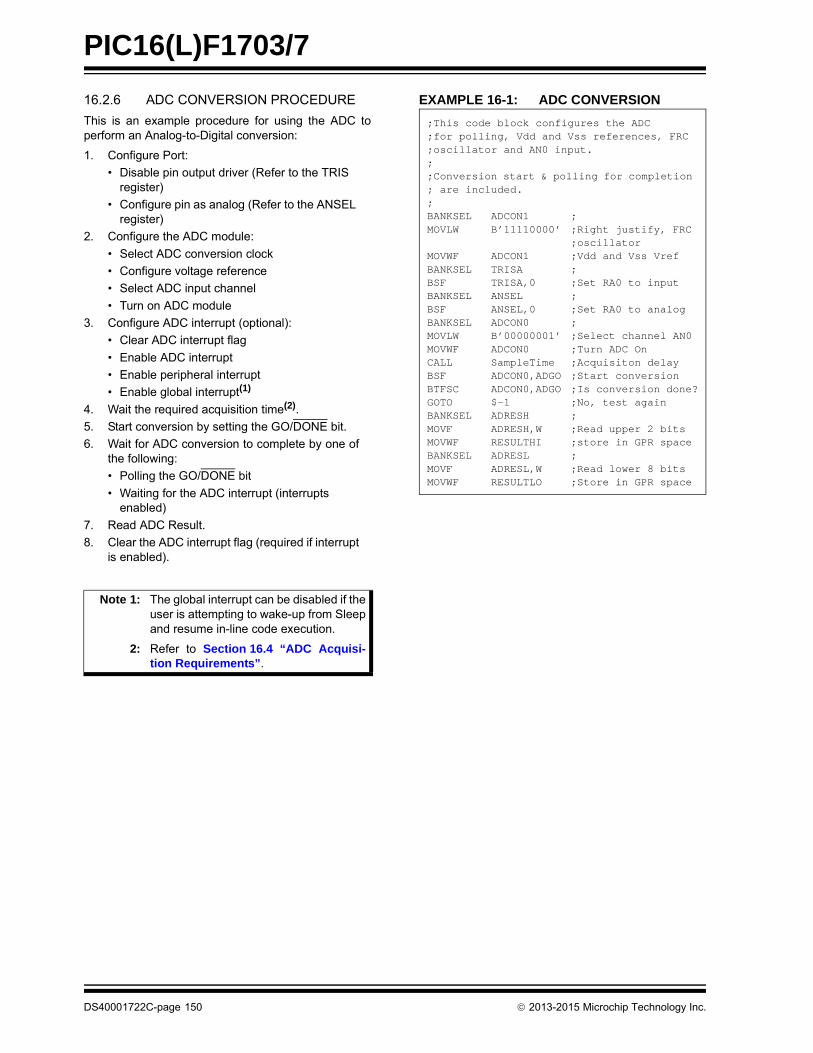
PIC16(L)F1703/7
16.2.6 ADC CONVERSION PROCEDURE
This is an example procedure for using the ADC toperform an Analog-to-Digital conversion:
1. Configure Port:
• Disable pin output driver (Refer to the TRIS register)
• Configure pin as analog (Refer to the ANSEL register)
2. Configure the ADC module:
• Select ADC conversion clock
• Configure voltage reference
• Select ADC input channel
• Turn on ADC module
3. Configure ADC interrupt (optional):
• Clear ADC interrupt flag
• Enable ADC interrupt
• Enable peripheral interrupt
• Enable global interrupt(1)
4. Wait the required acquisition time(2).
5. Start conversion by setting the GO/DONE bit.
6. Wait for ADC conversion to complete by one ofthe following:
• Polling the GO/DONE bit
• Waiting for the ADC interrupt (interrupts enabled)
7. Read ADC Result.
8. Clear the ADC interrupt flag (required if interruptis enabled).
EXAMPLE 16-1: ADC CONVERSION
Note 1: The global interrupt can be disabled if theuser is attempting to wake-up from Sleepand resume in-line code execution.
2: Refer to Section 16.4 “ADC Acquisi-tion Requirements”.
;This code block configures the ADC;for polling, Vdd and Vss references, FRC ;oscillator and AN0 input.;;Conversion start & polling for completion ; are included.;BANKSEL ADCON1 ;MOVLW B’11110000’ ;Right justify, FRC
;oscillatorMOVWF ADCON1 ;Vdd and Vss VrefBANKSEL TRISA ;BSF TRISA,0 ;Set RA0 to inputBANKSEL ANSEL ;BSF ANSEL,0 ;Set RA0 to analogBANKSEL ADCON0 ;MOVLW B’00000001’ ;Select channel AN0MOVWF ADCON0 ;Turn ADC OnCALL SampleTime ;Acquisiton delayBSF ADCON0,ADGO ;Start conversionBTFSC ADCON0,ADGO ;Is conversion done?GOTO $-1 ;No, test againBANKSEL ADRESH ;MOVF ADRESH,W ;Read upper 2 bitsMOVWF RESULTHI ;store in GPR spaceBANKSEL ADRESL ;MOVF ADRESL,W ;Read lower 8 bitsMOVWF RESULTLO ;Store in GPR space
DS40001722C-page 150 2013-2015 Microchip Technology Inc.
PIC16(L)F1703/7
16.3 Register Definitions: ADC Control
REGISTER 16-1: ADCON0: ADC CONTROL REGISTER 0
U-0 R/W-0/0 R/W-0/0 R/W-0/0 R/W-0/0 R/W-0/0 R/W-0/0 R/W-0/0
— CHS<4:0> GO/DONE ADON
bit 7 bit 0
Legend:
R = Readable bit W = Writable bit U = Unimplemented bit, read as ‘0’
u = Bit is unchanged x = Bit is unknown -n/n = Value at POR and BOR/Value at all other Resets
‘1’ = Bit is set ‘0’ = Bit is cleared
bit 7 Unimplemented: Read as ‘0’
bit 6-2 CHS<4:0>: Analog Channel Select bits
11111 = FVR (Fixed Voltage Reference) Buffer 1 Output(1)
11110 = Reserved11101 = Temperature Indicator(2)
11100 = Reserved. No channel connected. • • •
01100 = Reserved. No channel connected.01011 = AN1101010 = AN1001001 = AN901000 = AN800111 = AN700110 = AN600101 = AN500100 = AN400011 = AN300010 = AN200001 = AN100000 = AN0
bit 1 GO/DONE: ADC Conversion Status bit
1 = ADC conversion cycle in progress. Setting this bit starts an ADC conversion cycle. This bit is automatically cleared by hardware when the ADC conversion has completed.0 = ADC conversion completed/not in progress
bit 0 ADON: ADC Enable bit1 = ADC is enabled0 = ADC is disabled and consumes no operating current
Note 1: See Section 14.0 “Fixed Voltage Reference (FVR)” for more information.
2: See Section 15.0 “Temperature Indicator Module” for more information.
2013-2015 Microchip Technology Inc. DS40001722C-page 151
PIC16(L)F1703/7
REGISTER 16-2: ADCON1: ADC CONTROL REGISTER 1
R/W-0/0 R/W-0/0 R/W-0/0 R/W-0/0 U-0 R/W-0/0 R/W-0/0 R/W-0/0
ADFM ADCS<2:0> — ADNREF ADPREF<1:0>
bit 7 bit 0
Legend:
R = Readable bit W = Writable bit U = Unimplemented bit, read as ‘0’
u = Bit is unchanged x = Bit is unknown -n/n = Value at POR and BOR/Value at all other Resets
‘1’ = Bit is set ‘0’ = Bit is cleared
bit 7 ADFM: ADC Result Format Select bit1 = Right justified. Six Most Significant bits of ADRESH are set to ‘0’ when the conversion result is
loaded.0 = Left justified. Six Least Significant bits of ADRESL are set to ‘0’ when the conversion result is
loaded.
bit 6-4 ADCS<2:0>: ADC Conversion Clock Select bits111 = FRC (clock supplied from an internal RC oscillator)110 = FOSC/64101 = FOSC/16100 = FOSC/4011 = FRC (clock supplied from an internal RC oscillator)010 = FOSC/32001 = FOSC/8000 = FOSC/2
bit 3 Unimplemented: Read as ‘0’
bit 2 ADNREF: ADC Negative Voltage Reference Configuration bit0 = VREF- is connected to VSS
1 = VREF- is connected to VREF- pin
bit 1-0 ADPREF<1:0>: ADC Positive Voltage Reference Configuration bits11 = VREF+ is connected to internal FVR_Buffer1(1)
10 = VREF+ is connected to external VREF+ pin(1)
01 = Reserved00 = VREF+ is connected to VDD
Note 1: When selecting the VREF+ pin as the source of the positive reference, be aware that a minimum voltage specification exists. See Table 26-15 for details.
DS40001722C-page 152 2013-2015 Microchip Technology Inc.
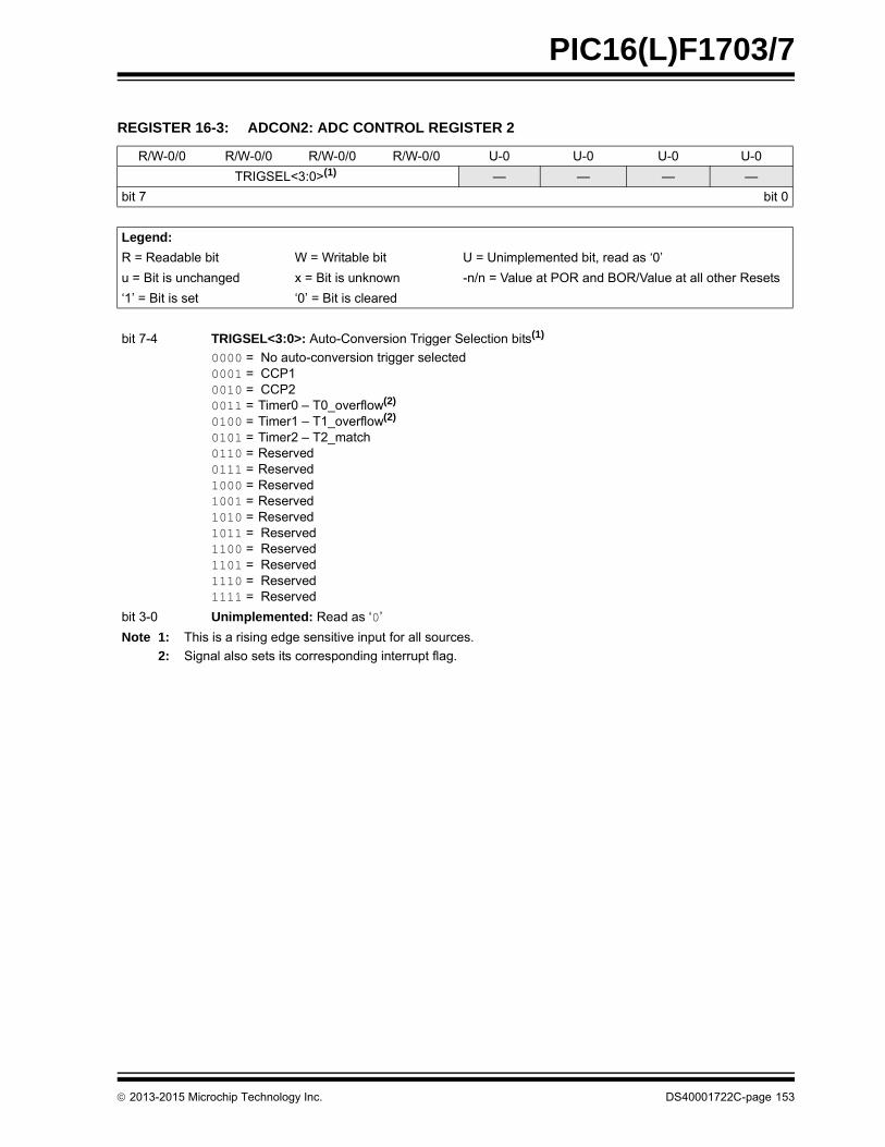
PIC16(L)F1703/7
REGISTER 16-3: ADCON2: ADC CONTROL REGISTER 2
R/W-0/0 R/W-0/0 R/W-0/0 R/W-0/0 U-0 U-0 U-0 U-0
TRIGSEL<3:0>(1) — — — —
bit 7 bit 0
Legend:
R = Readable bit W = Writable bit U = Unimplemented bit, read as ‘0’
u = Bit is unchanged x = Bit is unknown -n/n = Value at POR and BOR/Value at all other Resets
‘1’ = Bit is set ‘0’ = Bit is cleared
bit 7-4 TRIGSEL<3:0>: Auto-Conversion Trigger Selection bits(1)
0000 = No auto-conversion trigger selected0001 = CCP10010 = CCP20011 = Timer0 – T0_overflow(2)
0100 = Timer1 – T1_overflow(2)
0101 = Timer2 – T2_match0110 = Reserved0111 = Reserved1000 = Reserved1001 = Reserved1010 = Reserved1011 = Reserved1100 = Reserved1101 = Reserved1110 = Reserved1111 = Reserved
bit 3-0 Unimplemented: Read as ‘0’
Note 1: This is a rising edge sensitive input for all sources.
2: Signal also sets its corresponding interrupt flag.
2013-2015 Microchip Technology Inc. DS40001722C-page 153
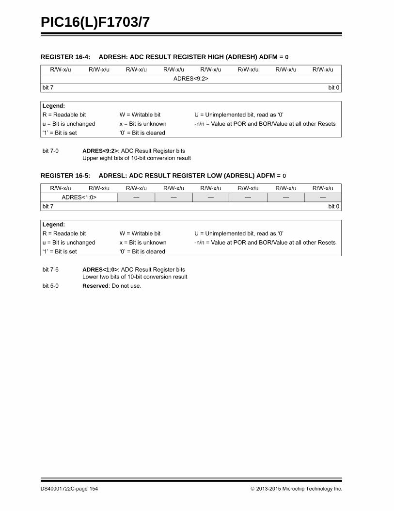
PIC16(L)F1703/7
REGISTER 16-4: ADRESH: ADC RESULT REGISTER HIGH (ADRESH) ADFM = 0
R/W-x/u R/W-x/u R/W-x/u R/W-x/u R/W-x/u R/W-x/u R/W-x/u R/W-x/u
ADRES<9:2>
bit 7 bit 0
Legend:
R = Readable bit W = Writable bit U = Unimplemented bit, read as ‘0’
u = Bit is unchanged x = Bit is unknown -n/n = Value at POR and BOR/Value at all other Resets
‘1’ = Bit is set ‘0’ = Bit is cleared
bit 7-0 ADRES<9:2>: ADC Result Register bitsUpper eight bits of 10-bit conversion result
REGISTER 16-5: ADRESL: ADC RESULT REGISTER LOW (ADRESL) ADFM = 0
R/W-x/u R/W-x/u R/W-x/u R/W-x/u R/W-x/u R/W-x/u R/W-x/u R/W-x/u
ADRES<1:0> — — — — — —
bit 7 bit 0
Legend:
R = Readable bit W = Writable bit U = Unimplemented bit, read as ‘0’
u = Bit is unchanged x = Bit is unknown -n/n = Value at POR and BOR/Value at all other Resets
‘1’ = Bit is set ‘0’ = Bit is cleared
bit 7-6 ADRES<1:0>: ADC Result Register bitsLower two bits of 10-bit conversion result
bit 5-0 Reserved: Do not use.
DS40001722C-page 154 2013-2015 Microchip Technology Inc.

PIC16(L)F1703/7
REGISTER 16-6: ADRESH: ADC RESULT REGISTER HIGH (ADRESH) ADFM = 1
R/W-x/u R/W-x/u R/W-x/u R/W-x/u R/W-x/u R/W-x/u R/W-x/u R/W-x/u
— — — — — — ADRES<9:8>
bit 7 bit 0
Legend:
R = Readable bit W = Writable bit U = Unimplemented bit, read as ‘0’
u = Bit is unchanged x = Bit is unknown -n/n = Value at POR and BOR/Value at all other Resets
‘1’ = Bit is set ‘0’ = Bit is cleared
bit 7-2 Reserved: Do not use.
bit 1-0 ADRES<9:8>: ADC Result Register bitsUpper two bits of 10-bit conversion result
REGISTER 16-7: ADRESL: ADC RESULT REGISTER LOW (ADRESL) ADFM = 1
R/W-x/u R/W-x/u R/W-x/u R/W-x/u R/W-x/u R/W-x/u R/W-x/u R/W-x/u
ADRES<7:0>
bit 7 bit 0
Legend:
R = Readable bit W = Writable bit U = Unimplemented bit, read as ‘0’
u = Bit is unchanged x = Bit is unknown -n/n = Value at POR and BOR/Value at all other Resets
‘1’ = Bit is set ‘0’ = Bit is cleared
bit 7-0 ADRES<7:0>: ADC Result Register bitsLower eight bits of 10-bit conversion result
2013-2015 Microchip Technology Inc. DS40001722C-page 155
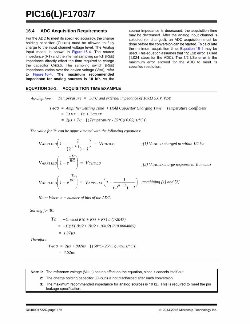
PIC16(L)F1703/7
16.4 ADC Acquisition Requirements
For the ADC to meet its specified accuracy, the chargeholding capacitor (CHOLD) must be allowed to fullycharge to the input channel voltage level. The AnalogInput model is shown in Figure 16-4. The sourceimpedance (RS) and the internal sampling switch (RSS)impedance directly affect the time required to chargethe capacitor CHOLD. The sampling switch (RSS)impedance varies over the device voltage (VDD), referto Figure 16-4. The maximum recommendedimpedance for analog sources is 10 k. As the
source impedance is decreased, the acquisition timemay be decreased. After the analog input channel isselected (or changed), an ADC acquisition must bedone before the conversion can be started. To calculatethe minimum acquisition time, Equation 16-1 may beused. This equation assumes that 1/2 LSb error is used(1,024 steps for the ADC). The 1/2 LSb error is themaximum error allowed for the ADC to meet itsspecified resolution.
EQUATION 16-1: ACQUISITION TIME EXAMPLE
TACQ Amplifier Settling Time Hold Capacitor Charging Time Temperature Coefficient+ +=
TAMP TC TCOFF+ +=
2µs TC Temperature - 25°C 0.05µs/°C + +=
TC CHOLD RIC RSS RS+ + ln(1/2047)–=
10pF 1k 7k 10k+ + – ln(0.0004885)=
1.37= µs
VAPPLIED 1 e
Tc–RC---------
–
VAPPLIED 11
2n 1+ 1–
--------------------------– =
VAPPLIED 11
2n 1+ 1–
--------------------------– VCHOLD=
VAPPLIED 1 e
TC–RC----------
–
VCHOLD=
;[1] VCHOLD charged to within 1/2 lsb
;[2] VCHOLD charge response to VAPPLIED
;combining [1] and [2]
The value for TC can be approximated with the following equations:
Solving for TC:
Therefore:
Temperature 50°C and external impedance of 10k 5.0V VDD=Assumptions:
Note: Where n = number of bits of the ADC.
TACQ 2µs 892ns 50°C- 25°C 0.05µs/°C + +=
4.62µs=
Note 1: The reference voltage (VREF) has no effect on the equation, since it cancels itself out.
2: The charge holding capacitor (CHOLD) is not discharged after each conversion.
3: The maximum recommended impedance for analog sources is 10 k. This is required to meet the pin leakage specification.
DS40001722C-page 156 2013-2015 Microchip Technology Inc.
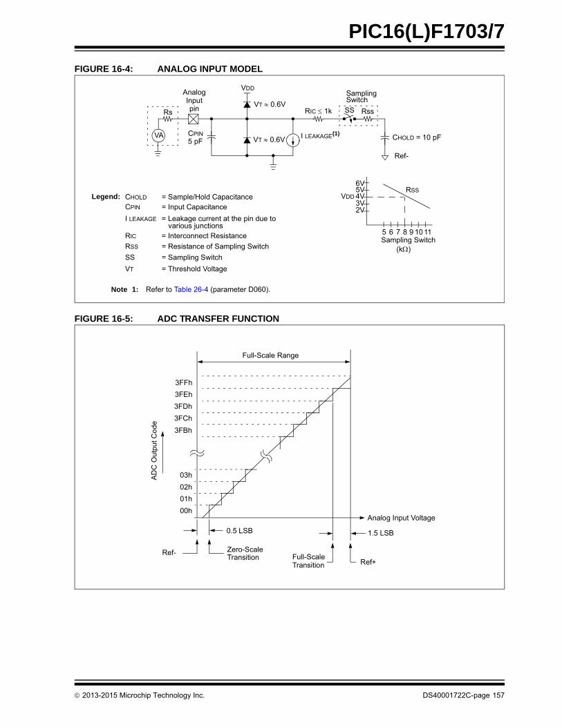
PIC16(L)F1703/7
FIGURE 16-4: ANALOG INPUT MODEL
FIGURE 16-5: ADC TRANSFER FUNCTION
CPINVA
Rs
Analog
5 pF
VDD
VT 0.6V
VT 0.6V I LEAKAGE(1)
RIC 1k
SamplingSwitch
SS Rss
CHOLD = 10 pF
Ref-
6V
Sampling Switch
5V4V3V2V
5 6 7 8 9 10 11
(k)
VDD
Legend:
CPIN
VT
I LEAKAGE
RIC
SS
CHOLD
= Input Capacitance
= Threshold Voltage
= Leakage current at the pin due to
= Interconnect Resistance
= Sampling Switch
= Sample/Hold Capacitance
various junctions
RSS
Note 1: Refer to Table 26-4 (parameter D060).
RSS = Resistance of Sampling Switch
Inputpin
3FFh
3FEh
AD
C O
utp
ut C
od
e
3FDh
3FCh
03h
02h
01h
00h
Full-Scale
3FBh
0.5 LSB
Ref- Zero-ScaleTransition
Ref+Transition
1.5 LSB
Full-Scale Range
Analog Input Voltage
2013-2015 Microchip Technology Inc. DS40001722C-page 157
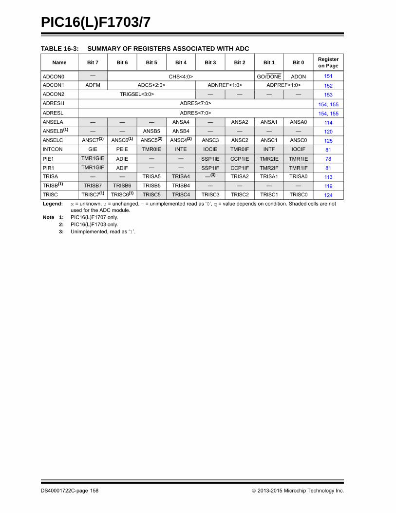
PIC16(L)F1703/7
TABLE 16-3: SUMMARY OF REGISTERS ASSOCIATED WITH ADC
Name Bit 7 Bit 6 Bit 5 Bit 4 Bit 3 Bit 2 Bit 1 Bit 0Register on Page
ADCON0 — CHS<4:0> GO/DONE ADON 151
ADCON1 ADFM ADCS<2:0> ADNREF<1:0> ADPREF<1:0> 152
ADCON2 TRIGSEL<3:0> — — — — 153
ADRESH ADRES<7:0> 154, 155
ADRESL ADRES<7:0> 154, 155
ANSELA — — — ANSA4 — ANSA2 ANSA1 ANSA0 114
ANSELB(1) — — ANSB5 ANSB4 — — — — 120
ANSELC ANSC7(1) ANSC6(1) ANSC5(2) ANSC4(2) ANSC3 ANSC2 ANSC1 ANSC0 125
INTCON GIE PEIE TMR0IE INTE IOCIE TMR0IF INTF IOCIF 81
PIE1 TMR1GIE ADIE — — SSP1IE CCP1IE TMR2IE TMR1IE 78
PIR1 TMR1GIF ADIF — — SSP1IF CCP1IF TMR2IF TMR1IF 81
TRISA — — TRISA5 TRISA4 —(3) TRISA2 TRISA1 TRISA0 113
TRISB(1) TRISB7 TRISB6 TRISB5 TRISB4 — — — — 119
TRISC TRISC7(1) TRISC6(1) TRISC5 TRISC4 TRISC3 TRISC2 TRISC1 TRISC0 124
Legend: x = unknown, u = unchanged, — = unimplemented read as ‘0’, q = value depends on condition. Shaded cells are not used for the ADC module.
Note 1: PIC16(L)F1707 only.2: PIC16(L)F1703 only.3: Unimplemented, read as ‘1’.
DS40001722C-page 158 2013-2015 Microchip Technology Inc.

PIC16(L)F1703/7
17.0 OPERATIONAL AMPLIFIER (OPA) MODULES
The Operational Amplifier (OPA) is a standard3-terminal device requiring external feedback tooperate. The OPA module has the following features:
• External connections to I/O ports
• Low leakage inputs
• Factory Calibrated Input Offset Voltage
FIGURE 17-1: OPAx MODULE BLOCK DIAGRAM
OPAReserved
OPAXEN
OPAXSP(1)
FVR_Buffer2
OPAxNCH<1:0>
OPAXOUTOPAxIN-
OPAxIN+ 0x
10
11 0
1
OPAXUG
Note 1: The OPAxSP bit must be set. Low-Power mode is not supported.
2013-2015 Microchip Technology Inc. DS40001722C-page 159
PIC16(L)F1703/7
17.1 OPA Module Performance
Common AC and DC performance specifications forthe OPA module:
• Common-Mode Voltage Range
• Leakage Current
• Input Offset Voltage
• Open Loop Gain
• Gain Bandwidth Product
Common-mode voltage range is the specified volt-age range for the OPA+ and OPA- inputs, for which theOPA module will perform to within its specifications.The OPA module is designed to operate with input volt-ages between VSS and VDD. Behavior forcommon-mode voltages greater than VDD, or belowVSS, are not guaranteed.
Leakage current is a measure of the small source orsink currents on the OPA+ and OPA- inputs. Tominimize the effect of leakage currents, the effectiveimpedances connected to the OPA+ and OPA- inputsshould be kept as small as possible and equal.
Input offset voltage is a measure of the voltagedifference between the OPA+ and OPA- inputs in aclosed loop circuit with the OPA in its linear region. Theoffset voltage will appear as a DC offset in the outputequal to the input offset voltage, multiplied by the gainof the circuit. The input offset voltage is also affected bythe common-mode voltage. The OPA is factorycalibrated to minimize the input offset voltage of themodule.
Open loop gain is the ratio of the output voltage to thedifferential input voltage, (OPA+) - (OPA-). The gain isgreatest at DC and falls off with frequency.
Gain Bandwidth Product or GBWP is the frequencyat which the open loop gain falls off to 0 dB.
17.1.1 OPA Module Control
The OPA module is enabled by setting the OPAxEN bitof the OPAxCON register. When enabled, the OPAforces the output driver of OPAxOUT pin into tri-state toprevent contention between the driver and the OPAoutput.
17.1.2 UNITY GAIN MODE
The OPAxUG bit of the OPAxCON register selects theUnity Gain mode. When unity gain is selected, the OPAoutput is connected to the inverting input and theOPAxIN pin is relinquished, releasing the pin forgeneral purpose input and output.
17.2 Effects of Reset
A device Reset forces all registers to their Reset state.This disables the OPA module.
Note: When the OPA module is enabled, theOPAxOUT pin is driven by the Op Ampoutput, not by the PORT digital driver.Refer to Table 26-16 for the Op Amp outputdrive capability.
DS40001722C-page 160 2013-2015 Microchip Technology Inc.
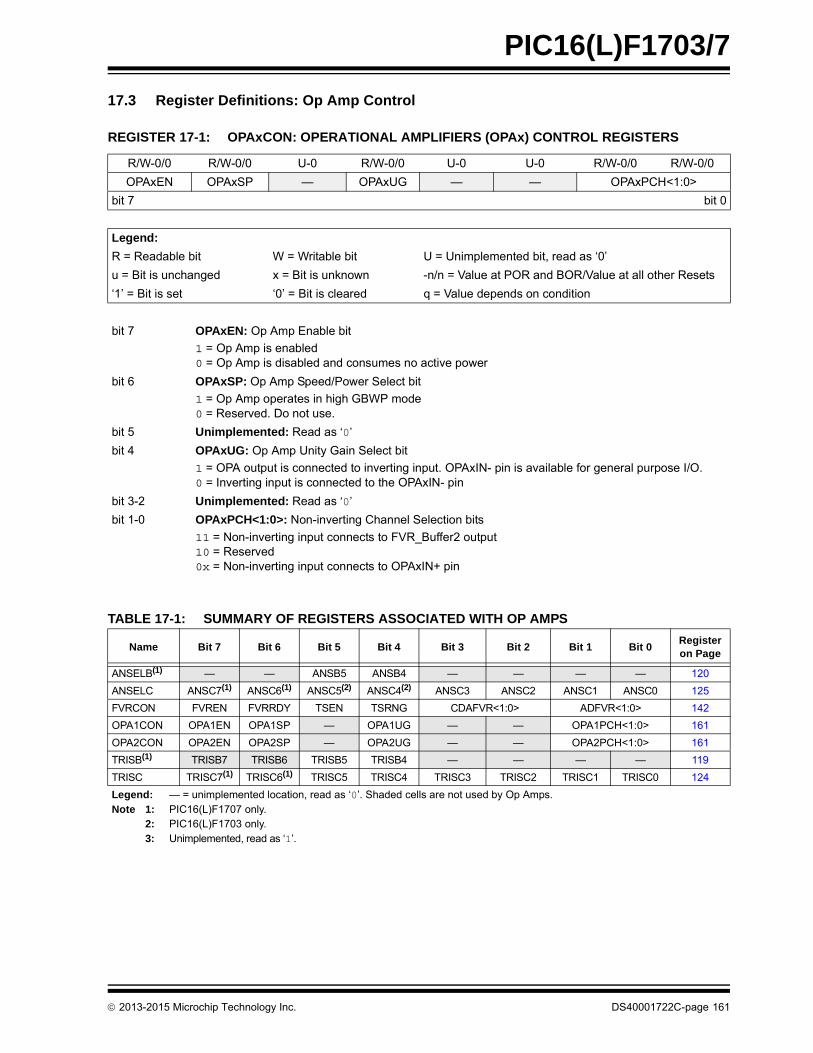
PIC16(L)F1703/7
17.3 Register Definitions: Op Amp Control
TABLE 17-1: SUMMARY OF REGISTERS ASSOCIATED WITH OP AMPS
REGISTER 17-1: OPAxCON: OPERATIONAL AMPLIFIERS (OPAx) CONTROL REGISTERS
R/W-0/0 R/W-0/0 U-0 R/W-0/0 U-0 U-0 R/W-0/0 R/W-0/0
OPAxEN OPAxSP — OPAxUG — — OPAxPCH<1:0>
bit 7 bit 0
Legend:
R = Readable bit W = Writable bit U = Unimplemented bit, read as ‘0’
u = Bit is unchanged x = Bit is unknown -n/n = Value at POR and BOR/Value at all other Resets
‘1’ = Bit is set ‘0’ = Bit is cleared q = Value depends on condition
bit 7 OPAxEN: Op Amp Enable bit
1 = Op Amp is enabled0 = Op Amp is disabled and consumes no active power
bit 6 OPAxSP: Op Amp Speed/Power Select bit
1 = Op Amp operates in high GBWP mode0 = Reserved. Do not use.
bit 5 Unimplemented: Read as ‘0’
bit 4 OPAxUG: Op Amp Unity Gain Select bit
1 = OPA output is connected to inverting input. OPAxIN- pin is available for general purpose I/O.0 = Inverting input is connected to the OPAxIN- pin
bit 3-2 Unimplemented: Read as ‘0’
bit 1-0 OPAxPCH<1:0>: Non-inverting Channel Selection bits
11 = Non-inverting input connects to FVR_Buffer2 output10 = Reserved0x = Non-inverting input connects to OPAxIN+ pin
Name Bit 7 Bit 6 Bit 5 Bit 4 Bit 3 Bit 2 Bit 1 Bit 0Register on Page
ANSELB(1) — — ANSB5 ANSB4 — — — — 120
ANSELC ANSC7(1) ANSC6(1) ANSC5(2) ANSC4(2) ANSC3 ANSC2 ANSC1 ANSC0 125
FVRCON FVREN FVRRDY TSEN TSRNG CDAFVR<1:0> ADFVR<1:0> 142
OPA1CON OPA1EN OPA1SP — OPA1UG — — OPA1PCH<1:0> 161
OPA2CON OPA2EN OPA2SP — OPA2UG — — OPA2PCH<1:0> 161
TRISB(1) TRISB7 TRISB6 TRISB5 TRISB4 — — — — 119
TRISC TRISC7(1) TRISC6(1) TRISC5 TRISC4 TRISC3 TRISC2 TRISC1 TRISC0 124
Legend: — = unimplemented location, read as ‘0’. Shaded cells are not used by Op Amps.Note 1: PIC16(L)F1707 only.
2: PIC16(L)F1703 only.3: Unimplemented, read as ‘1’.
2013-2015 Microchip Technology Inc. DS40001722C-page 161
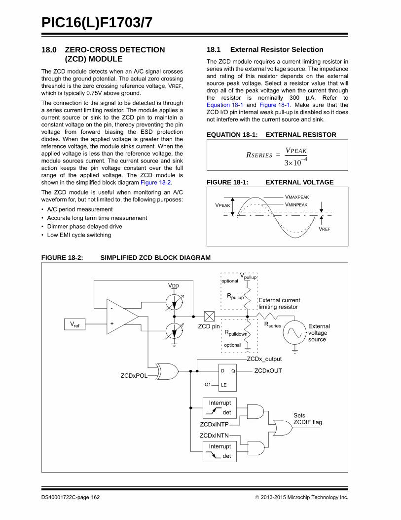
PIC16(L)F1703/7
18.0 ZERO-CROSS DETECTION (ZCD) MODULE
The ZCD module detects when an A/C signal crossesthrough the ground potential. The actual zero crossingthreshold is the zero crossing reference voltage, VREF,which is typically 0.75V above ground.
The connection to the signal to be detected is througha series current limiting resistor. The module applies acurrent source or sink to the ZCD pin to maintain aconstant voltage on the pin, thereby preventing the pinvoltage from forward biasing the ESD protectiondiodes. When the applied voltage is greater than thereference voltage, the module sinks current. When theapplied voltage is less than the reference voltage, themodule sources current. The current source and sinkaction keeps the pin voltage constant over the fullrange of the applied voltage. The ZCD module isshown in the simplified block diagram Figure 18-2.
The ZCD module is useful when monitoring an A/Cwaveform for, but not limited to, the following purposes:
• A/C period measurement
• Accurate long term time measurement
• Dimmer phase delayed drive
• Low EMI cycle switching
18.1 External Resistor Selection
The ZCD module requires a current limiting resistor inseries with the external voltage source. The impedanceand rating of this resistor depends on the externalsource peak voltage. Select a resistor value that willdrop all of the peak voltage when the current throughthe resistor is nominally 300 A. Refer toEquation 18-1 and Figure 18-1. Make sure that theZCD I/O pin internal weak pull-up is disabled so it doesnot interfere with the current source and sink.
EQUATION 18-1: EXTERNAL RESISTOR
FIGURE 18-1: EXTERNAL VOLTAGE
FIGURE 18-2: SIMPLIFIED ZCD BLOCK DIAGRAM
RSERIESVPEAK
34–10
-----------------=
VPEAK
VREF
VMAXPEAK
VMINPEAK
ZCD pin+
-
Vref
External currentlimiting resistor
Externalvoltagesource
Interrupt
det
Interrupt
det
ZCDxINTP
ZCDxINTN
SetsZCDIF flag
ZCDxOUT
Q1
D Q
LE
ZCDxPOL
ZCDx_output
VDD
Rseries
Rpullup
Vpullupoptional
Rpulldown
optional
DS40001722C-page 162 2013-2015 Microchip Technology Inc.
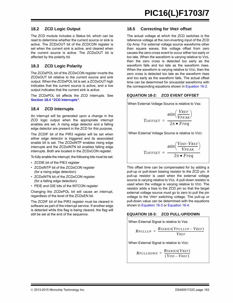
PIC16(L)F1703/7
18.2 ZCD Logic Output
The ZCD module includes a Status bit, which can beread to determine whether the current source or sink isactive. The ZCDxOUT bit of the ZCDCON register isset when the current sink is active, and cleared whenthe current source is active. The ZCDxOUT bit isaffected by the polarity bit.
18.3 ZCD Logic Polarity
The ZCDxPOL bit of the ZCDxCON register inverts theZCDxOUT bit relative to the current source and sinkoutput. When the ZCDxPOL bit is set, a ZCDxOUT highindicates that the current source is active, and a lowoutput indicates that the current sink is active.
The ZCDxPOL bit affects the ZCD interrupts. SeeSection 18.4 “ZCD Interrupts”.
18.4 ZCD Interrupts
An interrupt will be generated upon a change in theZCD logic output when the appropriate interruptenables are set. A rising edge detector and a fallingedge detector are present in the ZCD for this purpose.
The ZCDIF bit of the PIR3 register will be set wheneither edge detector is triggered and its associatedenable bit is set. The ZCDxINTP enables rising edgeinterrupts and the ZCDxINTN bit enables falling edgeinterrupts. Both are located in the ZCDxCON register.
To fully enable the interrupt, the following bits must be set:
• ZCDIE bit of the PIE3 register
• ZCDxINTP bit of the ZCDxCON register (for a rising edge detection)
• ZCDxINTN bit of the ZCDxCON register (for a falling edge detection)
• PEIE and GIE bits of the INTCON register
Changing the ZCDxPOL bit will cause an interrupt,regardless of the level of the ZCDxEN bit.
The ZCDIF bit of the PIR3 register must be cleared insoftware as part of the interrupt service. If another edgeis detected while this flag is being cleared, the flag willstill be set at the end of the sequence.
18.5 Correcting for VREF offset
The actual voltage at which the ZCD switches is thereference voltage at the non-inverting input of the ZCDOp Amp. For external voltage source waveforms otherthan square waves, this voltage offset from zerocauses the zero-cross event to occur either too early ortoo late. When the waveform is varying relative to VSS,then the zero cross is detected too early as thewaveform falls and too late as the waveform rises.When the waveform is varying relative to VDD, then thezero cross is detected too late as the waveform risesand too early as the waveform falls. The actual offsettime can be determined for sinusoidal waveforms withthe corresponding equations shown in Equation 18-2.
EQUATION 18-2: ZCD EVENT OFFSET
This offset time can be compensated for by adding apull-up or pull-down biasing resistor to the ZCD pin. Apull-up resistor is used when the external voltagesource is varying relative to VSS. A pull-down resistor isused when the voltage is varying relative to VDD. Theresistor adds a bias to the ZCD pin so that the targetexternal voltage source must go to zero to pull the pinvoltage to the VREF switching voltage. The pull-up orpull-down value can be determined with the equationsshown in Equation 18-3 or Equation 18-4.
EQUATION 18-3: ZCD PULL-UP/DOWN
TOFFSET
VREF
VPEAK---------------- asin
2 Freq--------------------------------=
When External Voltage Source is relative to Vss:
TOFFSET
VDD VREF–VPEAK
--------------------------- asin
2 Freq-------------------------------------------=
When External Voltage Source is relative to VDD:
RPULLUPRSERIES VPULLUP VREF–
VREF-----------------------------------------------------------------=
When External Signal is relative to Vss:
When External Signal is relative to VDD:
RPULLDOWNRSERIES VREF
VDD VREF– -------------------------------------=
2013-2015 Microchip Technology Inc. DS40001722C-page 163
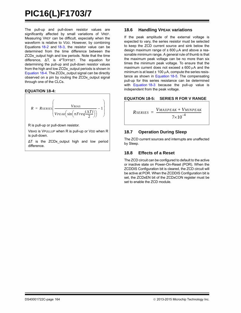
PIC16(L)F1703/7
The pull-up and pull-down resistor values aresignificantly affected by small variations of VREF.Measuring VREF can be difficult, especially when thewaveform is relative to VDD. However, by combiningEquations 18-2 and 18-3, the resistor value can bedetermined from the time difference between theZCDx_output high and low periods. Note that the timedifference, ∆T, is 4*TOFFSET. The equation fordetermining the pull-up and pull-down resistor valuesfrom the high and low ZCDx_output periods is shown inEquation 18-4. The ZCDx_output signal can be directlyobserved on a pin by routing the ZCDx_output signalthrough one of the CLCs.
EQUATION 18-4:
18.6 Handling VPEAK variations
If the peak amplitude of the external voltage isexpected to vary, the series resistor must be selectedto keep the ZCD current source and sink below thedesign maximum range of ± 600 A and above a rea-sonable minimum range. A general rule of thumb is thatthe maximum peak voltage can be no more than sixtimes the minimum peak voltage. To ensure that themaximum current does not exceed ± 600 A and theminimum is at least ± 100 A, compute the series resis-tance as shown in Equation 18-5. The compensatingpull-up for this series resistance can be determinedwith Equation 18-3 because the pull-up value isindependent from the peak voltage.
EQUATION 18-5: SERIES R FOR V RANGE
18.7 Operation During Sleep
The ZCD current sources and interrupts are unaffectedby Sleep.
18.8 Effects of a Reset
The ZCD circuit can be configured to default to the activeor inactive state on Power-On-Reset (POR). When theZCDDIS Configuration bit is cleared, the ZCD circuit willbe active at POR. When the ZCDDIS Configuration bit isset, the ZCDxEN bit of the ZCDxCON register must beset to enable the ZCD module.
R RSERIESVBIAS
VPEAK FreqT 2
------------ sin
---------------------------------------------------------------- 1–
=
R is pull-up or pull-down resistor.
VBIAS is VPULLUP when R is pull-up or VDD when Ris pull-down.
∆T is the ZCDx_output high and low perioddifference.
RSERIESVMAXPEAK VMINPEAK+
74–10
---------------------------------------------------------=
DS40001722C-page 164 2013-2015 Microchip Technology Inc.

PIC16(L)F1703/7
18.9 Register Definitions: ZCD Control
TABLE 18-1: SUMMARY OF REGISTERS ASSOCIATED WITH THE ZCD MODULE
TABLE 18-2: SUMMARY OF CONFIGURATION BITS ASSOCIATED WITH THE ZCD MODULE
REGISTER 18-1: ZCDxCON: ZERO CROSS DETECTION CONTROL REGISTER
R/W-q/q U-0 R-x/x R/W-0/0 U-0 U-0 R/W-0/0 R/W-0/0
ZCDxEN — ZCDxOUT ZCDxPOL — — ZCDxINTP ZCDxINTN
bit 7 bit 0
Legend:
R = Readable bit W = Writable bit U = Unimplemented bit, read as ‘0’
u = Bit is unchanged x = Bit is unknown -n/n = Value at POR and BOR/Value at all other Resets
‘1’ = Bit is set ‘0’ = Bit is cleared q = value depends on configuration bits
bit 7 ZCDxEN: Zero-Cross Detection Enable bit
1 = Zero-cross detect is enabled. ZCD pin is forced to output to source and sink current.0 = Zero-cross detect is disabled. ZCD pin operates according to PPS and TRIS controls.
bit 6 Unimplemented: Read as ‘0’
bit 5 ZCDxOUT: Zero-Cross Detection Logic Level bit
ZCDxPOL bit = 0:1 = ZCD pin is sinking current0 = ZCD pin is sourcing currentZCDxPOL bit = 1:1 = ZCD pin is sourcing current0 = ZCD pin is sinking current
bit 4 ZCDxPOL: Zero-Cross Detection Logic Output Polarity bit1 = ZCD logic output is inverted0 = ZCD logic output is not inverted
bit 3-2 Unimplemented: Read as ‘0’
bit 1 ZCDxINTP: Zero-Cross Positive Edge Interrupt Enable bit
1 = ZCDIF bit is set on low-to-high ZCDx_output transition0 = ZCDIF bit is unaffected by low-to-high ZCDx_output transition
bit 0 ZCDxINTN: Zero-Cross Negative Edge Interrupt Enable bit
1 = ZCDIF bit is set on high-to-low ZCDx_output transition0 = ZCDIF bit is unaffected by high-to-low ZCDx_output transition
Name Bit 7 Bit 6 Bit 5 Bit 4 Bit 3 Bit 2 Bit 1 Bit 0Register on page
PIE3 — — — ZCDIE — — — — 80
PIR3 — — — ZCDIF — — — — 83
ZCD1CON ZCD1EN — ZCD1OUT ZCD1POL — — ZCD1INTP ZCD1INTN 165
Legend: — = unimplemented, read as ‘0’. Shaded cells are unused by the ZCD module.
Name Bits Bit -/7 Bit -/6 Bit 13/5 Bit 12/4 Bit 11/3 Bit 10/2 Bit 9/1 Bit 8/0Register on Page
CONFIG213:8 — — LVP DEBUG LPBOR BORV STVREN PLLEN
507:0 ZCDDIS — — — — PPS1WAY WRT<1:0>
Legend: — = unimplemented location, read as ‘0’. Shaded cells are not used by ZCD module.
2013-2015 Microchip Technology Inc. DS40001722C-page 165
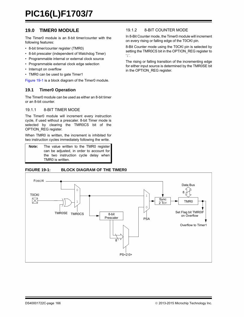
PIC16(L)F1703/7
19.0 TIMER0 MODULE
The Timer0 module is an 8-bit timer/counter with thefollowing features:
• 8-bit timer/counter register (TMR0)
• 8-bit prescaler (independent of Watchdog Timer)
• Programmable internal or external clock source
• Programmable external clock edge selection
• Interrupt on overflow
• TMR0 can be used to gate Timer1
Figure 19-1 is a block diagram of the Timer0 module.
19.1 Timer0 Operation
The Timer0 module can be used as either an 8-bit timeror an 8-bit counter.
19.1.1 8-BIT TIMER MODE
The Timer0 module will increment every instructioncycle, if used without a prescaler. 8-bit Timer mode isselected by clearing the TMR0CS bit of theOPTION_REG register.
When TMR0 is written, the increment is inhibited fortwo instruction cycles immediately following the write.
19.1.2 8-BIT COUNTER MODE
In 8-Bit Counter mode, the Timer0 module will incrementon every rising or falling edge of the T0CKI pin.
8-Bit Counter mode using the T0CKI pin is selected bysetting the TMR0CS bit in the OPTION_REG register to‘1’.
The rising or falling transition of the incrementing edgefor either input source is determined by the TMR0SE bitin the OPTION_REG register.
FIGURE 19-1: BLOCK DIAGRAM OF THE TIMER0
Note: The value written to the TMR0 registercan be adjusted, in order to account forthe two instruction cycle delay whenTMR0 is written.
T0CKI
TMR0SE
TMR0
PS<2:0>
Data Bus
Set Flag bit TMR0IFon OverflowTMR0CS
0
1
0
18
8
8-bitPrescaler
FOSC/4
PSA
Sync2 TCY
Overflow to Timer1
DS40001722C-page 166 2013-2015 Microchip Technology Inc.
PIC16(L)F1703/7
19.1.3 SOFTWARE PROGRAMMABLE PRESCALER
A software programmable prescaler is available forexclusive use with Timer0. The prescaler is enabled byclearing the PSA bit of the OPTION_REG register.
There are eight prescaler options for the Timer0 mod-ule ranging from 1:2 to 1:256. The prescale values areselectable via the PS<2:0> bits of the OPTION_REGregister. In order to have a 1:1 prescaler value for theTimer0 module, the prescaler must be disabled bysetting the PSA bit of the OPTION_REG register.
The prescaler is not readable or writable. All instructionswriting to the TMR0 register will clear the prescaler.
19.1.4 TIMER0 INTERRUPT
Timer0 will generate an interrupt when the TMR0register overflows from FFh to 00h. The TMR0IFinterrupt flag bit of the INTCON register is set everytime the TMR0 register overflows, regardless ofwhether or not the Timer0 interrupt is enabled. TheTMR0IF bit can only be cleared in software. The Timer0interrupt enable is the TMR0IE bit of the INTCONregister.
19.1.5 8-BIT COUNTER MODE SYNCHRONIZATION
When in 8-Bit Counter mode, the incrementing edge onthe T0CKI pin must be synchronized to the instructionclock. Synchronization can be accomplished bysampling the prescaler output on the Q2 and Q4 cyclesof the instruction clock. The high and low periods of theexternal clocking source must meet the timingrequirements as shown in Table 26-12.
19.1.6 OPERATION DURING SLEEP
Timer0 cannot operate while the processor is in Sleepmode. The contents of the TMR0 register will remainunchanged while the processor is in Sleep mode.
Note: The Watchdog Timer (WDT) uses its ownindependent prescaler.
Note: The Timer0 interrupt cannot wake theprocessor from Sleep since the timer isfrozen during Sleep.
2013-2015 Microchip Technology Inc. DS40001722C-page 167
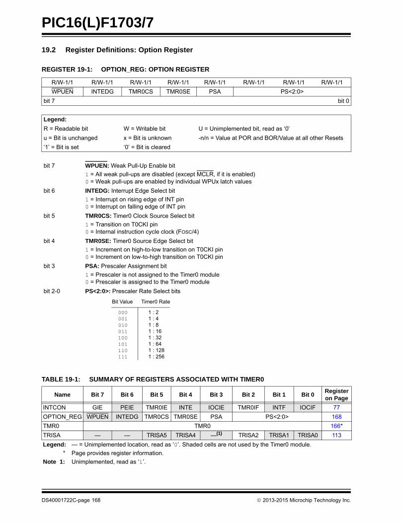
PIC16(L)F1703/7
19.2 Register Definitions: Option Register
TABLE 19-1: SUMMARY OF REGISTERS ASSOCIATED WITH TIMER0
REGISTER 19-1: OPTION_REG: OPTION REGISTER
R/W-1/1 R/W-1/1 R/W-1/1 R/W-1/1 R/W-1/1 R/W-1/1 R/W-1/1 R/W-1/1
WPUEN INTEDG TMR0CS TMR0SE PSA PS<2:0>
bit 7 bit 0
Legend:
R = Readable bit W = Writable bit U = Unimplemented bit, read as ‘0’
u = Bit is unchanged x = Bit is unknown -n/n = Value at POR and BOR/Value at all other Resets
‘1’ = Bit is set ‘0’ = Bit is cleared
bit 7 WPUEN: Weak Pull-Up Enable bit
1 = All weak pull-ups are disabled (except MCLR, if it is enabled)0 = Weak pull-ups are enabled by individual WPUx latch values
bit 6 INTEDG: Interrupt Edge Select bit
1 = Interrupt on rising edge of INT pin0 = Interrupt on falling edge of INT pin
bit 5 TMR0CS: Timer0 Clock Source Select bit
1 = Transition on T0CKI pin0 = Internal instruction cycle clock (FOSC/4)
bit 4 TMR0SE: Timer0 Source Edge Select bit
1 = Increment on high-to-low transition on T0CKI pin0 = Increment on low-to-high transition on T0CKI pin
bit 3 PSA: Prescaler Assignment bit
1 = Prescaler is not assigned to the Timer0 module0 = Prescaler is assigned to the Timer0 module
bit 2-0 PS<2:0>: Prescaler Rate Select bits
Name Bit 7 Bit 6 Bit 5 Bit 4 Bit 3 Bit 2 Bit 1 Bit 0Register on Page
INTCON GIE PEIE TMR0IE INTE IOCIE TMR0IF INTF IOCIF 77
OPTION_REG WPUEN INTEDG TMR0CS TMR0SE PSA PS<2:0> 168
TMR0 TMR0 166*
TRISA — — TRISA5 TRISA4 —(1) TRISA2 TRISA1 TRISA0 113
Legend: — = Unimplemented location, read as ‘0’. Shaded cells are not used by the Timer0 module.
* Page provides register information.
Note 1: Unimplemented, read as ‘1’.
000001010011100101110111
1 : 21 : 41 : 81 : 161 : 321 : 641 : 1281 : 256
Bit Value Timer0 Rate
DS40001722C-page 168 2013-2015 Microchip Technology Inc.
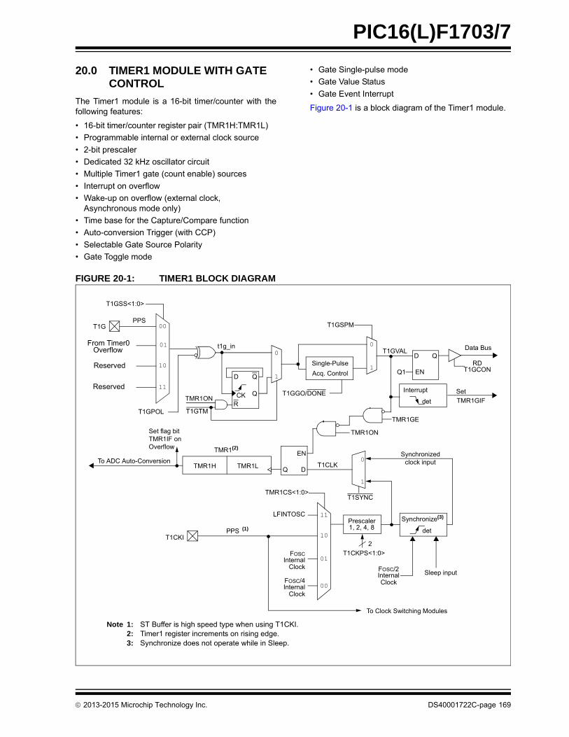
PIC16(L)F1703/7
20.0 TIMER1 MODULE WITH GATE CONTROL
The Timer1 module is a 16-bit timer/counter with thefollowing features:
• 16-bit timer/counter register pair (TMR1H:TMR1L)
• Programmable internal or external clock source
• 2-bit prescaler
• Dedicated 32 kHz oscillator circuit
• Multiple Timer1 gate (count enable) sources
• Interrupt on overflow
• Wake-up on overflow (external clock, Asynchronous mode only)
• Time base for the Capture/Compare function
• Auto-conversion Trigger (with CCP)
• Selectable Gate Source Polarity
• Gate Toggle mode
• Gate Single-pulse mode
• Gate Value Status
• Gate Event Interrupt
Figure 20-1 is a block diagram of the Timer1 module.
FIGURE 20-1: TIMER1 BLOCK DIAGRAM
TMR1H TMR1L
T1SYNC
T1CKPS<1:0>
Prescaler1, 2, 4, 8
0
1
Synchronizedclock input
2
TMR1(2)
TMR1ON
Note 1: ST Buffer is high speed type when using T1CKI.2: Timer1 register increments on rising edge.3: Synchronize does not operate while in Sleep.
T1G
FOSC/4Internal
Clock
T1CKI
TMR1CS<1:0>
(1)
Synchronize(3)
det
Sleep input
TMR1GE
0
1
00
01
10
11
T1GPOL
D
QCK
Q
0
1
T1GVAL
T1GTM
Single-Pulse
Acq. Control
T1GSPM
T1GGO/DONE
T1GSS<1:0>
10
11
00
01FOSC
InternalClock
R
D
EN
Q
Q1RD
T1GCON
Data Bus
det
Interrupt
TMR1GIF
Set
T1CLK
FOSC/2InternalClock
D
EN
Q
t1g_in
TMR1ON
LFINTOSC
From Timer0 Overflow
Reserved
Reserved
To Clock Switching Modules
Set flag bitTMR1IF onOverflow
To ADC Auto-Conversion
PPS
PPS
2013-2015 Microchip Technology Inc. DS40001722C-page 169
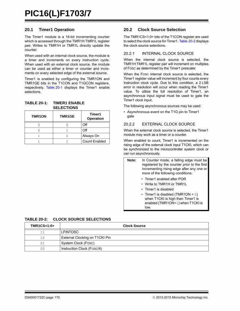
PIC16(L)F1703/7
20.1 Timer1 Operation
The Timer1 module is a 16-bit incrementing counterwhich is accessed through the TMR1H:TMR1L registerpair. Writes to TMR1H or TMR1L directly update thecounter.
When used with an internal clock source, the module isa timer and increments on every instruction cycle.When used with an external clock source, the modulecan be used as either a timer or counter and incre-ments on every selected edge of the external source.
Timer1 is enabled by configuring the TMR1ON andTMR1GE bits in the T1CON and T1GCON registers,respectively. Table 20-1 displays the Timer1 enableselections.
20.2 Clock Source Selection
The TMR1CS<1:0> bits of the T1CON register are usedto select the clock source for Timer1. Table 20-2 displaysthe clock source selections.
20.2.1 INTERNAL CLOCK SOURCE
When the internal clock source is selected, theTMR1H:TMR1L register pair will increment on multiplesof FOSC as determined by the Timer1 prescaler.
When the FOSC internal clock source is selected, theTimer1 register value will increment by four counts everyinstruction clock cycle. Due to this condition, a 2 LSBerror in resolution will occur when reading the Timer1value. To utilize the full resolution of Timer1, anasynchronous input signal must be used to gate theTimer1 clock input.
The following asynchronous sources may be used:
• Asynchronous event on the T1G pin to Timer1 gate
20.2.2 EXTERNAL CLOCK SOURCE
When the external clock source is selected, the Timer1module may work as a timer or a counter.
When enabled to count, Timer1 is incremented on therising edge of the external clock input T1CKI, which canbe synchronized to the microcontroller system clock orcan run asynchronously.
TABLE 20-1: TIMER1 ENABLE SELECTIONS
TMR1ON TMR1GETimer1
Operation
0 0 Off
0 1 Off
1 0 Always On
1 1 Count Enabled
Note: In Counter mode, a falling edge must beregistered by the counter prior to the firstincrementing rising edge after any one ormore of the following conditions:
• Timer1 enabled after POR
• Write to TMR1H or TMR1L
• Timer1 is disabled
• Timer1 is disabled (TMR1ON = 0) when T1CKI is high then Timer1 is enabled (TMR1ON=1) when T1CKI is low.
TABLE 20-2: CLOCK SOURCE SELECTIONS
TMR1CS<1:0> Clock Source
11 LFINTOSC
10 External Clocking on T1CKI Pin
01 System Clock (FOSC)
00 Instruction Clock (FOSC/4)
DS40001722C-page 170 2013-2015 Microchip Technology Inc.
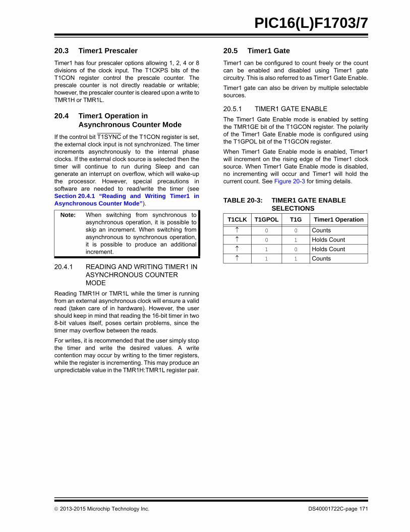
PIC16(L)F1703/7
20.3 Timer1 Prescaler
Timer1 has four prescaler options allowing 1, 2, 4 or 8divisions of the clock input. The T1CKPS bits of theT1CON register control the prescale counter. Theprescale counter is not directly readable or writable;however, the prescaler counter is cleared upon a write toTMR1H or TMR1L.
20.4 Timer1 Operation in Asynchronous Counter Mode
If the control bit T1SYNC of the T1CON register is set,the external clock input is not synchronized. The timerincrements asynchronously to the internal phaseclocks. If the external clock source is selected then thetimer will continue to run during Sleep and cangenerate an interrupt on overflow, which will wake-upthe processor. However, special precautions insoftware are needed to read/write the timer (seeSection 20.4.1 “Reading and Writing Timer1 inAsynchronous Counter Mode”).
20.4.1 READING AND WRITING TIMER1 IN ASYNCHRONOUS COUNTER MODE
Reading TMR1H or TMR1L while the timer is runningfrom an external asynchronous clock will ensure a validread (taken care of in hardware). However, the usershould keep in mind that reading the 16-bit timer in two8-bit values itself, poses certain problems, since thetimer may overflow between the reads.
For writes, it is recommended that the user simply stopthe timer and write the desired values. A writecontention may occur by writing to the timer registers,while the register is incrementing. This may produce anunpredictable value in the TMR1H:TMR1L register pair.
20.5 Timer1 Gate
Timer1 can be configured to count freely or the countcan be enabled and disabled using Timer1 gatecircuitry. This is also referred to as Timer1 Gate Enable.
Timer1 gate can also be driven by multiple selectablesources.
20.5.1 TIMER1 GATE ENABLE
The Timer1 Gate Enable mode is enabled by settingthe TMR1GE bit of the T1GCON register. The polarityof the Timer1 Gate Enable mode is configured usingthe T1GPOL bit of the T1GCON register.
When Timer1 Gate Enable mode is enabled, Timer1will increment on the rising edge of the Timer1 clocksource. When Timer1 Gate Enable mode is disabled,no incrementing will occur and Timer1 will hold thecurrent count. See Figure 20-3 for timing details.
Note: When switching from synchronous toasynchronous operation, it is possible toskip an increment. When switching fromasynchronous to synchronous operation,it is possible to produce an additionalincrement.
TABLE 20-3: TIMER1 GATE ENABLE SELECTIONS
T1CLK T1GPOL T1G Timer1 Operation
0 0 Counts
0 1 Holds Count
1 0 Holds Count
1 1 Counts
2013-2015 Microchip Technology Inc. DS40001722C-page 171
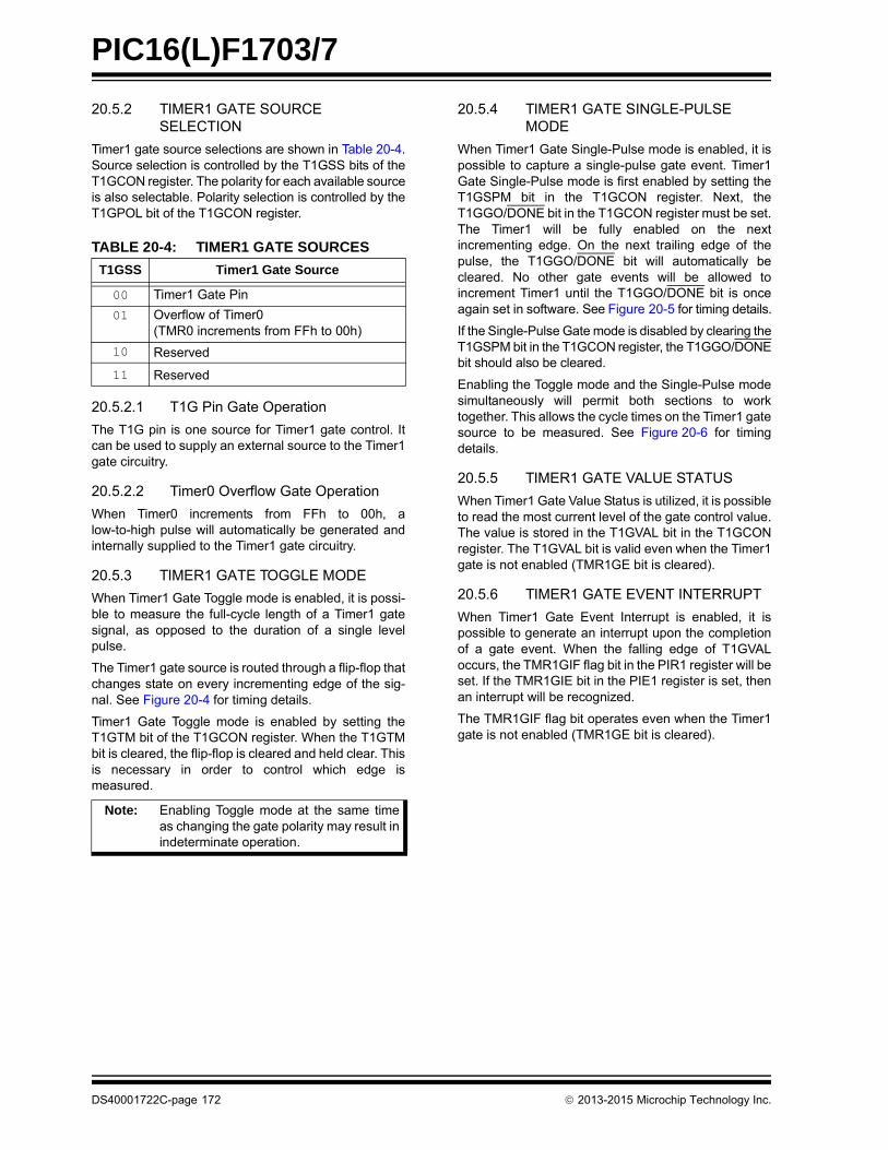
PIC16(L)F1703/7
20.5.2 TIMER1 GATE SOURCE SELECTION
Timer1 gate source selections are shown in Table 20-4.Source selection is controlled by the T1GSS bits of theT1GCON register. The polarity for each available sourceis also selectable. Polarity selection is controlled by theT1GPOL bit of the T1GCON register.
TABLE 20-4: TIMER1 GATE SOURCES
20.5.2.1 T1G Pin Gate Operation
The T1G pin is one source for Timer1 gate control. Itcan be used to supply an external source to the Timer1gate circuitry.
20.5.2.2 Timer0 Overflow Gate Operation
When Timer0 increments from FFh to 00h, alow-to-high pulse will automatically be generated andinternally supplied to the Timer1 gate circuitry.
20.5.3 TIMER1 GATE TOGGLE MODE
When Timer1 Gate Toggle mode is enabled, it is possi-ble to measure the full-cycle length of a Timer1 gatesignal, as opposed to the duration of a single levelpulse.
The Timer1 gate source is routed through a flip-flop thatchanges state on every incrementing edge of the sig-nal. See Figure 20-4 for timing details.
Timer1 Gate Toggle mode is enabled by setting theT1GTM bit of the T1GCON register. When the T1GTMbit is cleared, the flip-flop is cleared and held clear. Thisis necessary in order to control which edge ismeasured.
20.5.4 TIMER1 GATE SINGLE-PULSE MODE
When Timer1 Gate Single-Pulse mode is enabled, it ispossible to capture a single-pulse gate event. Timer1Gate Single-Pulse mode is first enabled by setting theT1GSPM bit in the T1GCON register. Next, theT1GGO/DONE bit in the T1GCON register must be set.The Timer1 will be fully enabled on the nextincrementing edge. On the next trailing edge of thepulse, the T1GGO/DONE bit will automatically becleared. No other gate events will be allowed toincrement Timer1 until the T1GGO/DONE bit is onceagain set in software. See Figure 20-5 for timing details.
If the Single-Pulse Gate mode is disabled by clearing theT1GSPM bit in the T1GCON register, the T1GGO/DONEbit should also be cleared.
Enabling the Toggle mode and the Single-Pulse modesimultaneously will permit both sections to worktogether. This allows the cycle times on the Timer1 gatesource to be measured. See Figure 20-6 for timingdetails.
20.5.5 TIMER1 GATE VALUE STATUS
When Timer1 Gate Value Status is utilized, it is possibleto read the most current level of the gate control value.The value is stored in the T1GVAL bit in the T1GCONregister. The T1GVAL bit is valid even when the Timer1gate is not enabled (TMR1GE bit is cleared).
20.5.6 TIMER1 GATE EVENT INTERRUPT
When Timer1 Gate Event Interrupt is enabled, it ispossible to generate an interrupt upon the completionof a gate event. When the falling edge of T1GVALoccurs, the TMR1GIF flag bit in the PIR1 register will beset. If the TMR1GIE bit in the PIE1 register is set, thenan interrupt will be recognized.
The TMR1GIF flag bit operates even when the Timer1gate is not enabled (TMR1GE bit is cleared).
T1GSS Timer1 Gate Source
00 Timer1 Gate Pin
01 Overflow of Timer0(TMR0 increments from FFh to 00h)
10 Reserved
11 Reserved
Note: Enabling Toggle mode at the same timeas changing the gate polarity may result inindeterminate operation.
DS40001722C-page 172 2013-2015 Microchip Technology Inc.
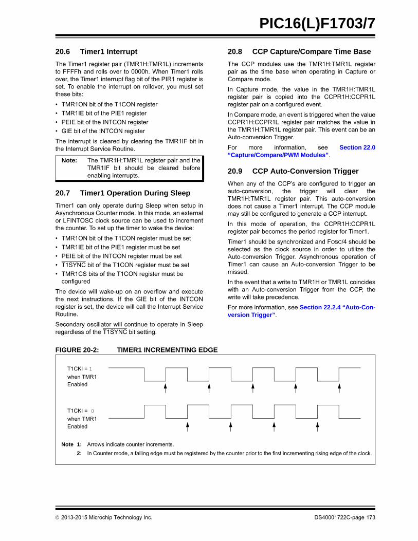
PIC16(L)F1703/7
20.6 Timer1 Interrupt
The Timer1 register pair (TMR1H:TMR1L) incrementsto FFFFh and rolls over to 0000h. When Timer1 rollsover, the Timer1 interrupt flag bit of the PIR1 register isset. To enable the interrupt on rollover, you must setthese bits:
• TMR1ON bit of the T1CON register
• TMR1IE bit of the PIE1 register
• PEIE bit of the INTCON register
• GIE bit of the INTCON register
The interrupt is cleared by clearing the TMR1IF bit inthe Interrupt Service Routine.
20.7 Timer1 Operation During Sleep
Timer1 can only operate during Sleep when setup inAsynchronous Counter mode. In this mode, an externalor LFINTOSC clock source can be used to incrementthe counter. To set up the timer to wake the device:
• TMR1ON bit of the T1CON register must be set
• TMR1IE bit of the PIE1 register must be set
• PEIE bit of the INTCON register must be set
• T1SYNC bit of the T1CON register must be set
• TMR1CS bits of the T1CON register must be configured
The device will wake-up on an overflow and executethe next instructions. If the GIE bit of the INTCONregister is set, the device will call the Interrupt ServiceRoutine.
Secondary oscillator will continue to operate in Sleepregardless of the T1SYNC bit setting.
20.8 CCP Capture/Compare Time Base
The CCP modules use the TMR1H:TMR1L registerpair as the time base when operating in Capture orCompare mode.
In Capture mode, the value in the TMR1H:TMR1Lregister pair is copied into the CCPR1H:CCPR1Lregister pair on a configured event.
In Compare mode, an event is triggered when the valueCCPR1H:CCPR1L register pair matches the value inthe TMR1H:TMR1L register pair. This event can be anAuto-conversion Trigger.
For more information, see Section 22.0“Capture/Compare/PWM Modules”.
20.9 CCP Auto-Conversion Trigger
When any of the CCP’s are configured to trigger anauto-conversion, the trigger will clear theTMR1H:TMR1L register pair. This auto-conversiondoes not cause a Timer1 interrupt. The CCP modulemay still be configured to generate a CCP interrupt.
In this mode of operation, the CCPR1H:CCPR1Lregister pair becomes the period register for Timer1.
Timer1 should be synchronized and FOSC/4 should beselected as the clock source in order to utilize theAuto-conversion Trigger. Asynchronous operation ofTimer1 can cause an Auto-conversion Trigger to bemissed.
In the event that a write to TMR1H or TMR1L coincideswith an Auto-conversion Trigger from the CCP, thewrite will take precedence.
For more information, see Section 22.2.4 “Auto-Con-version Trigger”.
FIGURE 20-2: TIMER1 INCREMENTING EDGE
Note: The TMR1H:TMR1L register pair and theTMR1IF bit should be cleared beforeenabling interrupts.
T1CKI = 1
when TMR1Enabled
T1CKI = 0
when TMR1Enabled
Note 1: Arrows indicate counter increments.
2: In Counter mode, a falling edge must be registered by the counter prior to the first incrementing rising edge of the clock.
2013-2015 Microchip Technology Inc. DS40001722C-page 173
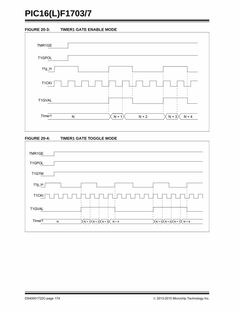
PIC16(L)F1703/7
FIGURE 20-3: TIMER1 GATE ENABLE MODE
FIGURE 20-4: TIMER1 GATE TOGGLE MODE
TMR1GE
T1GPOL
t1g_in
T1CKI
T1GVAL
Timer1 N N + 1 N + 2 N + 3 N + 4
TMR1GE
T1GPOL
T1GTM
t1g_in
T1CKI
T1GVAL
Timer1 N N + 1 N + 2 N + 3 N + 4 N + 5 N + 6 N + 7 N + 8
DS40001722C-page 174 2013-2015 Microchip Technology Inc.
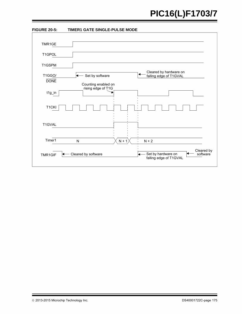
PIC16(L)F1703/7
FIGURE 20-5: TIMER1 GATE SINGLE-PULSE MODE
TMR1GE
T1GPOL
t1g_in
T1CKI
T1GVAL
Timer1 N N + 1 N + 2
T1GSPM
T1GGO/
DONE
Set by softwareCleared by hardware onfalling edge of T1GVAL
Set by hardware onfalling edge of T1GVAL
Cleared by softwareCleared bysoftwareTMR1GIF
Counting enabled onrising edge of T1G
2013-2015 Microchip Technology Inc. DS40001722C-page 175

PIC16(L)F1703/7
FIGURE 20-6: TIMER1 GATE SINGLE-PULSE AND TOGGLE COMBINED MODE
TMR1GE
T1GPOL
t1g_in
T1CKI
T1GVAL
Timer1 N N + 1 N + 2
T1GSPM
T1GGO/
DONE
Set by softwareCleared by hardware onfalling edge of T1GVAL
Set by hardware onfalling edge of T1GVALCleared by software
Cleared bysoftwareTMR1GIF
T1GTM
Counting enabled onrising edge of T1G
N + 4N + 3
DS40001722C-page 176 2013-2015 Microchip Technology Inc.
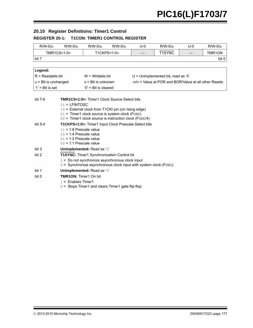
PIC16(L)F1703/7
20.10 Register Definitions: Timer1 Control
REGISTER 20-1: T1CON: TIMER1 CONTROL REGISTER
R/W-0/u R/W-0/u R/W-0/u R/W-0/u U-0 R/W-0/u U-0 R/W-0/u
TMR1CS<1:0> T1CKPS<1:0> — T1SYNC — TMR1ON
bit 7 bit 0
Legend:
R = Readable bit W = Writable bit U = Unimplemented bit, read as ‘0’
u = Bit is unchanged x = Bit is unknown -n/n = Value at POR and BOR/Value at all other Resets
‘1’ = Bit is set ‘0’ = Bit is cleared
bit 7-6 TMR1CS<1:0>: Timer1 Clock Source Select bits
11 = LFINTOSC10 = External clock from T1CKI pin (on rising edge)01 = Timer1 clock source is system clock (FOSC)00 = Timer1 clock source is instruction clock (FOSC/4)
bit 5-4 T1CKPS<1:0>: Timer1 Input Clock Prescale Select bits
11 = 1:8 Prescale value10 = 1:4 Prescale value01 = 1:2 Prescale value00 = 1:1 Prescale value
bit 3 Unimplemented: Read as ‘0’
bit 2 T1SYNC: Timer1 Synchronization Control bit
1 = Do not synchronize asynchronous clock input0 = Synchronize asynchronous clock input with system clock (FOSC)
bit 1 Unimplemented: Read as ‘0’
bit 0 TMR1ON: Timer1 On bit
1 = Enables Timer10 = Stops Timer1 and clears Timer1 gate flip-flop
2013-2015 Microchip Technology Inc. DS40001722C-page 177
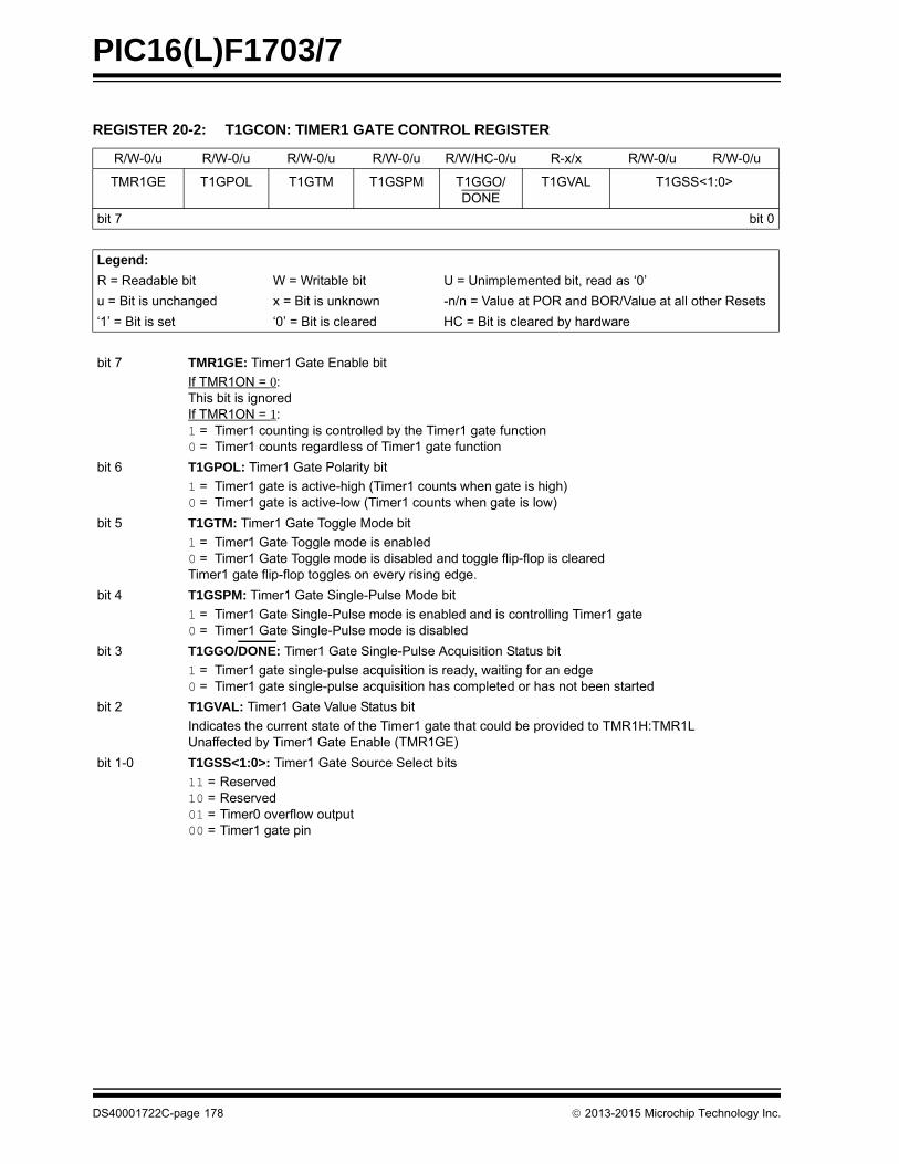
PIC16(L)F1703/7
REGISTER 20-2: T1GCON: TIMER1 GATE CONTROL REGISTER
R/W-0/u R/W-0/u R/W-0/u R/W-0/u R/W/HC-0/u R-x/x R/W-0/u R/W-0/u
TMR1GE T1GPOL T1GTM T1GSPM T1GGO/DONE
T1GVAL T1GSS<1:0>
bit 7 bit 0
Legend:
R = Readable bit W = Writable bit U = Unimplemented bit, read as ‘0’
u = Bit is unchanged x = Bit is unknown -n/n = Value at POR and BOR/Value at all other Resets
‘1’ = Bit is set ‘0’ = Bit is cleared HC = Bit is cleared by hardware
bit 7 TMR1GE: Timer1 Gate Enable bit
If TMR1ON = 0:This bit is ignoredIf TMR1ON = 1:1 = Timer1 counting is controlled by the Timer1 gate function0 = Timer1 counts regardless of Timer1 gate function
bit 6 T1GPOL: Timer1 Gate Polarity bit
1 = Timer1 gate is active-high (Timer1 counts when gate is high)0 = Timer1 gate is active-low (Timer1 counts when gate is low)
bit 5 T1GTM: Timer1 Gate Toggle Mode bit
1 = Timer1 Gate Toggle mode is enabled0 = Timer1 Gate Toggle mode is disabled and toggle flip-flop is clearedTimer1 gate flip-flop toggles on every rising edge.
bit 4 T1GSPM: Timer1 Gate Single-Pulse Mode bit
1 = Timer1 Gate Single-Pulse mode is enabled and is controlling Timer1 gate0 = Timer1 Gate Single-Pulse mode is disabled
bit 3 T1GGO/DONE: Timer1 Gate Single-Pulse Acquisition Status bit
1 = Timer1 gate single-pulse acquisition is ready, waiting for an edge0 = Timer1 gate single-pulse acquisition has completed or has not been started
bit 2 T1GVAL: Timer1 Gate Value Status bit
Indicates the current state of the Timer1 gate that could be provided to TMR1H:TMR1LUnaffected by Timer1 Gate Enable (TMR1GE)
bit 1-0 T1GSS<1:0>: Timer1 Gate Source Select bits
11 = Reserved10 = Reserved01 = Timer0 overflow output00 = Timer1 gate pin
DS40001722C-page 178 2013-2015 Microchip Technology Inc.
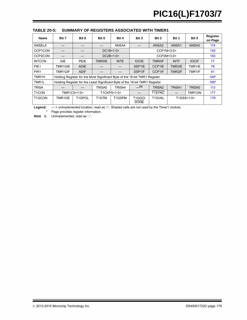
PIC16(L)F1703/7
TABLE 20-5: SUMMARY OF REGISTERS ASSOCIATED WITH TIMER1
Name Bit 7 Bit 6 Bit 5 Bit 4 Bit 3 Bit 2 Bit 1 Bit 0Register on Page
ANSELA — — — ANSA4 — ANSA2 ANSA1 ANSA0 114
CCP1CON — — DC1B<1:0> CCP1M<3:0> 193
CCP2CON — — DC2B<1:0> CCP2M<3:0> 193
INTCON GIE PEIE TMR0IE INTE IOCIE TMR0IF INTF IOCIF 77
PIE1 TMR1GIE ADIE — — SSP1IE CCP1IE TMR2IE TMR1IE 78
PIR1 TMR1GIF ADIF — — SSP1IF CCP1IF TMR2IF TMR1IF 81
TMR1H Holding Register for the Most Significant Byte of the 16-bit TMR1 Register 169*
TMR1L Holding Register for the Least Significant Byte of the 16-bit TMR1 Register 169*
TRISA — — TRISA5 TRISA4 —(1) TRISA2 TRISA1 TRISA0 113
T1CON TMR1CS<1:0> T1CKPS<1:0> — T1SYNC — TMR1ON 177
T1GCON TMR1GE T1GPOL T1GTM T1GSPM T1GGO/DONE
T1GVAL T1GSS<1:0> 178
Legend: — = unimplemented location, read as ‘0’. Shaded cells are not used by the Timer1 module.* Page provides register information.
Note 1: Unimplemented, read as ‘1’.
2013-2015 Microchip Technology Inc. DS40001722C-page 179
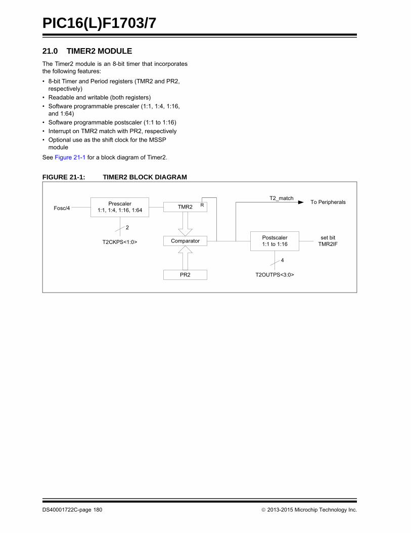
PIC16(L)F1703/7
21.0 TIMER2 MODULE
The Timer2 module is an 8-bit timer that incorporatesthe following features:
• 8-bit Timer and Period registers (TMR2 and PR2, respectively)
• Readable and writable (both registers)
• Software programmable prescaler (1:1, 1:4, 1:16, and 1:64)
• Software programmable postscaler (1:1 to 1:16)
• Interrupt on TMR2 match with PR2, respectively
• Optional use as the shift clock for the MSSP module
See Figure 21-1 for a block diagram of Timer2.
FIGURE 21-1: TIMER2 BLOCK DIAGRAM
Prescaler1:1, 1:4, 1:16, 1:64Fosc/4
2
T2CKPS<1:0> ComparatorPostscaler1:1 to 1:16
4
T2OUTPS<3:0>
set bitTMR2IF
TMR2 R
PR2
T2_matchTo Peripherals
DS40001722C-page 180 2013-2015 Microchip Technology Inc.

PIC16(L)F1703/7
21.1 Timer2 Operation
The clock input to the Timer2 modules is the systeminstruction clock (FOSC/4).
TMR2 increments from 00h on each clock edge.
A 4-bit counter/prescaler on the clock input allows directinput, divide-by-4 and divide-by-16 prescale options.These options are selected by the prescaler control bits,T2CKPS<1:0> of the T2CON register. The value ofTMR2 is compared to that of the Period register, PR2, oneach clock cycle. When the two values match, thecomparator generates a match signal as the timeroutput. This signal also resets the value of TMR2 to 00hon the next cycle and drives the outputcounter/postscaler (see Section 21.2 “Timer2Interrupt”).
The TMR2 and PR2 registers are both directly readableand writable. The TMR2 register is cleared on anydevice Reset, whereas the PR2 register initializes toFFh. Both the prescaler and postscaler counters arecleared on the following events:
• a write to the TMR2 register
• a write to the T2CON register
• Power-on Reset (POR)
• Brown-out Reset (BOR)
• MCLR Reset
• Watchdog Timer (WDT) Reset
• Stack Overflow Reset
• Stack Underflow Reset
• RESET Instruction
21.2 Timer2 Interrupt
Timer2 can also generate an optional device interrupt.The Timer2 output signal (TMR2-to-PR2 match)provides the input for the 4-bit counter/postscaler. Thiscounter generates the TMR2 match interrupt flag whichis latched in TMR2IF of the PIR1 register. The interruptis enabled by setting the TMR2 Match Interrupt Enablebit, TMR2IE, of the PIE1 register.
A range of 16 postscale options (from 1:1 through 1:16inclusive) can be selected with the postscaler controlbits, T2OUTPS<3:0>, of the T2CON register.
21.3 Timer2 Output
The unscaled output of TMR2 is available primarily tothe CCP modules, where it is used as a time base foroperations in PWM mode.
Timer2 can be optionally used as the shift clock sourcefor the MSSP module operating in SPI mode.Additional information is provided in Section 23.0“Master Synchronous Serial Port (MSSP) Module”
21.4 Timer2 Operation During Sleep
The Timer2 timers cannot be operated while theprocessor is in Sleep mode. The contents of the TMR2and PR2 registers will remain unchanged while theprocessor is in Sleep mode.
Note: TMR2 is not cleared when T2CON iswritten.
2013-2015 Microchip Technology Inc. DS40001722C-page 181
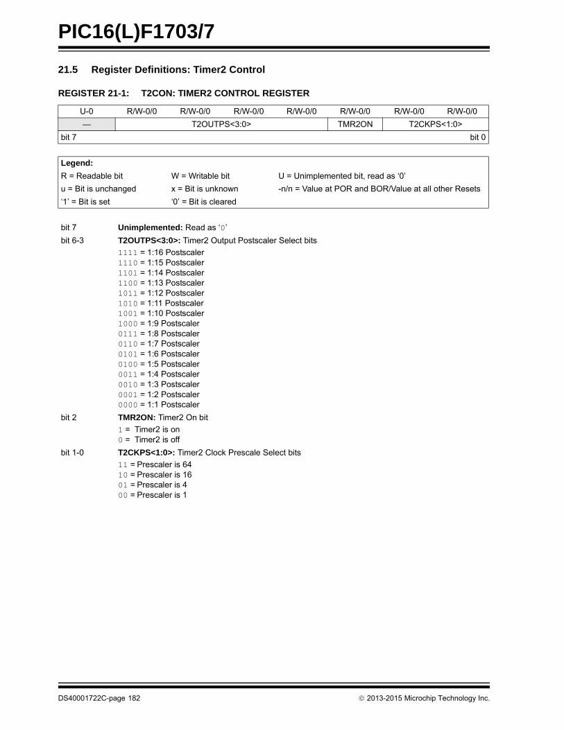
PIC16(L)F1703/7
21.5 Register Definitions: Timer2 Control
REGISTER 21-1: T2CON: TIMER2 CONTROL REGISTER
U-0 R/W-0/0 R/W-0/0 R/W-0/0 R/W-0/0 R/W-0/0 R/W-0/0 R/W-0/0
— T2OUTPS<3:0> TMR2ON T2CKPS<1:0>
bit 7 bit 0
Legend:
R = Readable bit W = Writable bit U = Unimplemented bit, read as ‘0’
u = Bit is unchanged x = Bit is unknown -n/n = Value at POR and BOR/Value at all other Resets
‘1’ = Bit is set ‘0’ = Bit is cleared
bit 7 Unimplemented: Read as ‘0’
bit 6-3 T2OUTPS<3:0>: Timer2 Output Postscaler Select bits
1111 = 1:16 Postscaler1110 = 1:15 Postscaler1101 = 1:14 Postscaler1100 = 1:13 Postscaler1011 = 1:12 Postscaler1010 = 1:11 Postscaler1001 = 1:10 Postscaler1000 = 1:9 Postscaler0111 = 1:8 Postscaler0110 = 1:7 Postscaler0101 = 1:6 Postscaler0100 = 1:5 Postscaler0011 = 1:4 Postscaler0010 = 1:3 Postscaler0001 = 1:2 Postscaler0000 = 1:1 Postscaler
bit 2 TMR2ON: Timer2 On bit
1 = Timer2 is on0 = Timer2 is off
bit 1-0 T2CKPS<1:0>: Timer2 Clock Prescale Select bits
11 = Prescaler is 6410 = Prescaler is 1601 = Prescaler is 400 = Prescaler is 1
DS40001722C-page 182 2013-2015 Microchip Technology Inc.
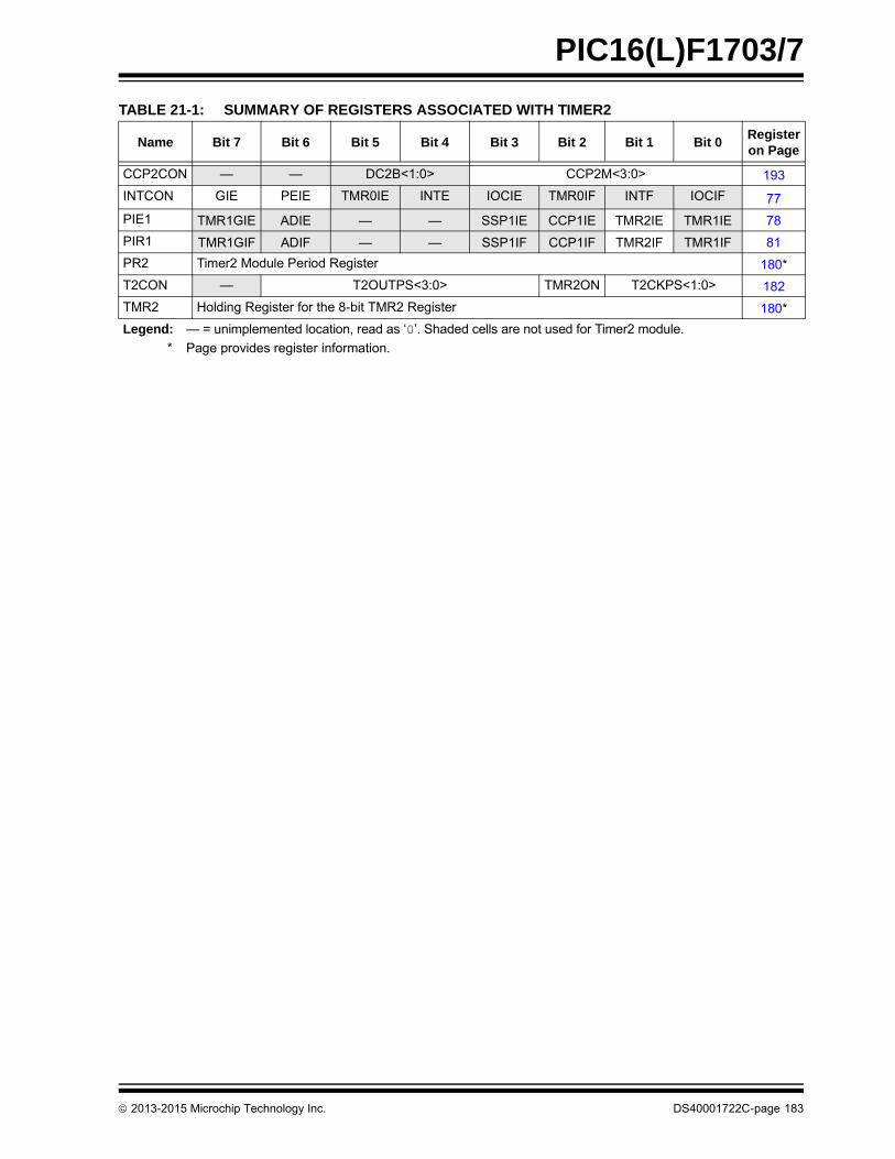
PIC16(L)F1703/7
TABLE 21-1: SUMMARY OF REGISTERS ASSOCIATED WITH TIMER2
Name Bit 7 Bit 6 Bit 5 Bit 4 Bit 3 Bit 2 Bit 1 Bit 0Register on Page
CCP2CON — — DC2B<1:0> CCP2M<3:0> 193
INTCON GIE PEIE TMR0IE INTE IOCIE TMR0IF INTF IOCIF 77
PIE1 TMR1GIE ADIE — — SSP1IE CCP1IE TMR2IE TMR1IE 78
PIR1 TMR1GIF ADIF — — SSP1IF CCP1IF TMR2IF TMR1IF 81
PR2 Timer2 Module Period Register 180*
T2CON — T2OUTPS<3:0> TMR2ON T2CKPS<1:0> 182
TMR2 Holding Register for the 8-bit TMR2 Register 180*
Legend: — = unimplemented location, read as ‘0’. Shaded cells are not used for Timer2 module.
* Page provides register information.
2013-2015 Microchip Technology Inc. DS40001722C-page 183

PIC16(L)F1703/7
22.0 CAPTURE/COMPARE/PWM MODULES
The Capture/Compare/PWM module is a peripheralwhich allows the user to time and control differentevents, and to generate Pulse-Width Modulation(PWM) signals. In Capture mode, the peripheral allowsthe timing of the duration of an event. The Comparemode allows the user to trigger an external event whena predetermined amount of time has expired. ThePWM mode can generate Pulse-Width Modulatedsignals of varying frequency and duty cycle.
This family of devices contains two standardCapture/Compare/PWM modules (CCP1 and CCP2).
The Capture and Compare functions are identical for allCCP modules.
Note 1: In devices with more than one CCPmodule, it is very important to pay closeattention to the register names used. Anumber placed after the module acronymis used to distinguish between separatemodules. For example, the CCP1CONand CCP2CON control the sameoperational aspects of two completelydifferent CCP modules.
2: Throughout this section, genericreferences to a CCP module in any of itsoperating modes may be interpreted asbeing equally applicable to CCPx module.Register names, module signals, I/O pins,and bit names may use the genericdesignator ‘x’ to indicate the use of anumeral to distinguish a particular module,when required.
DS40001722C-page 184 2013-2015 Microchip Technology Inc.
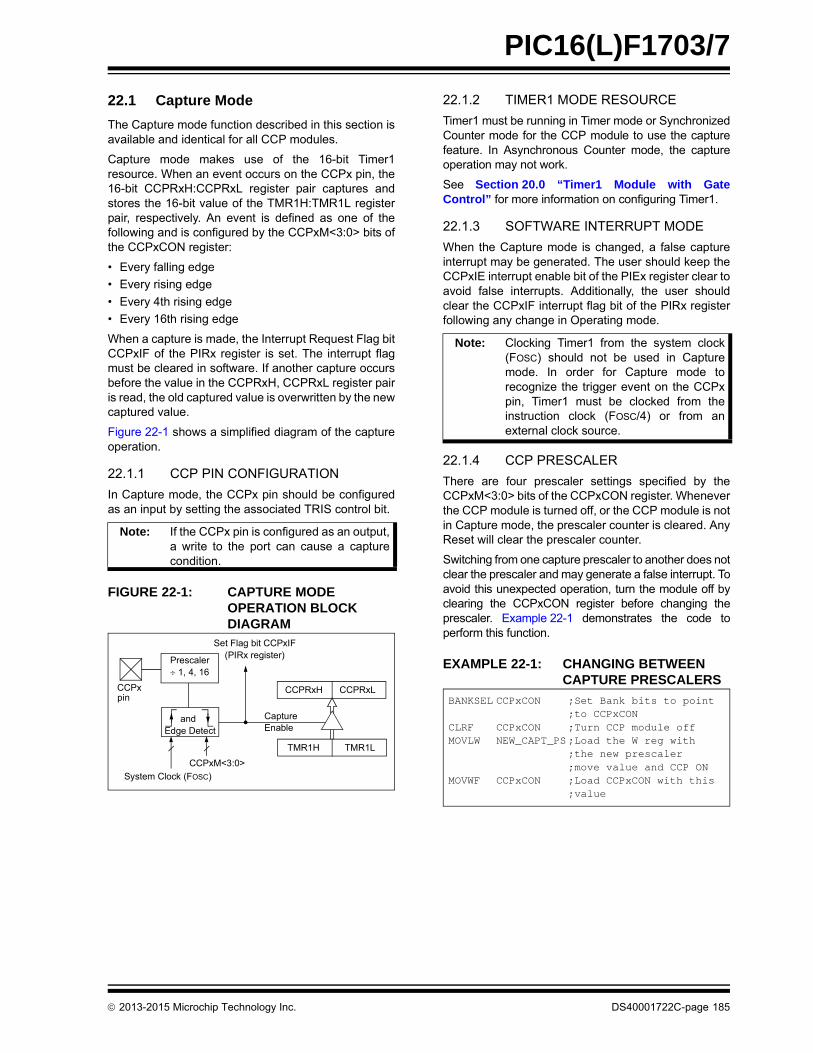
PIC16(L)F1703/7
22.1 Capture Mode
The Capture mode function described in this section isavailable and identical for all CCP modules.
Capture mode makes use of the 16-bit Timer1resource. When an event occurs on the CCPx pin, the16-bit CCPRxH:CCPRxL register pair captures andstores the 16-bit value of the TMR1H:TMR1L registerpair, respectively. An event is defined as one of thefollowing and is configured by the CCPxM<3:0> bits ofthe CCPxCON register:
• Every falling edge
• Every rising edge
• Every 4th rising edge
• Every 16th rising edge
When a capture is made, the Interrupt Request Flag bitCCPxIF of the PIRx register is set. The interrupt flagmust be cleared in software. If another capture occursbefore the value in the CCPRxH, CCPRxL register pairis read, the old captured value is overwritten by the newcaptured value.
Figure 22-1 shows a simplified diagram of the captureoperation.
22.1.1 CCP PIN CONFIGURATION
In Capture mode, the CCPx pin should be configuredas an input by setting the associated TRIS control bit.
FIGURE 22-1: CAPTURE MODE OPERATION BLOCK DIAGRAM
22.1.2 TIMER1 MODE RESOURCE
Timer1 must be running in Timer mode or SynchronizedCounter mode for the CCP module to use the capturefeature. In Asynchronous Counter mode, the captureoperation may not work.
See Section 20.0 “Timer1 Module with GateControl” for more information on configuring Timer1.
22.1.3 SOFTWARE INTERRUPT MODE
When the Capture mode is changed, a false captureinterrupt may be generated. The user should keep theCCPxIE interrupt enable bit of the PIEx register clear toavoid false interrupts. Additionally, the user shouldclear the CCPxIF interrupt flag bit of the PIRx registerfollowing any change in Operating mode.
22.1.4 CCP PRESCALER
There are four prescaler settings specified by theCCPxM<3:0> bits of the CCPxCON register. Wheneverthe CCP module is turned off, or the CCP module is notin Capture mode, the prescaler counter is cleared. AnyReset will clear the prescaler counter.
Switching from one capture prescaler to another does notclear the prescaler and may generate a false interrupt. Toavoid this unexpected operation, turn the module off byclearing the CCPxCON register before changing theprescaler. Example 22-1 demonstrates the code toperform this function.
EXAMPLE 22-1: CHANGING BETWEEN CAPTURE PRESCALERS
Note: If the CCPx pin is configured as an output,a write to the port can cause a capturecondition.
CCPRxH CCPRxL
TMR1H TMR1L
Set Flag bit CCPxIF(PIRx register)
CaptureEnable
CCPxM<3:0>
Prescaler 1, 4, 16
andEdge Detect
pinCCPx
System Clock (FOSC)
Note: Clocking Timer1 from the system clock(FOSC) should not be used in Capturemode. In order for Capture mode torecognize the trigger event on the CCPxpin, Timer1 must be clocked from theinstruction clock (FOSC/4) or from anexternal clock source.
BANKSEL CCPxCON ;Set Bank bits to point;to CCPxCON
CLRF CCPxCON ;Turn CCP module offMOVLW NEW_CAPT_PS;Load the W reg with
;the new prescaler;move value and CCP ON
MOVWF CCPxCON ;Load CCPxCON with this;value
2013-2015 Microchip Technology Inc. DS40001722C-page 185
PIC16(L)F1703/7
22.1.5 CAPTURE DURING SLEEP
Capture mode depends upon the Timer1 module forproper operation. There are two options for driving theTimer1 module in Capture mode. It can be driven by theinstruction clock (FOSC/4), or by an external clock source.
When Timer1 is clocked by FOSC/4, Timer1 will notincrement during Sleep. When the device wakes fromSleep, Timer1 will continue from its previous state.
Capture mode will operate during Sleep when Timer1is clocked by an external clock source.
DS40001722C-page 186 2013-2015 Microchip Technology Inc.
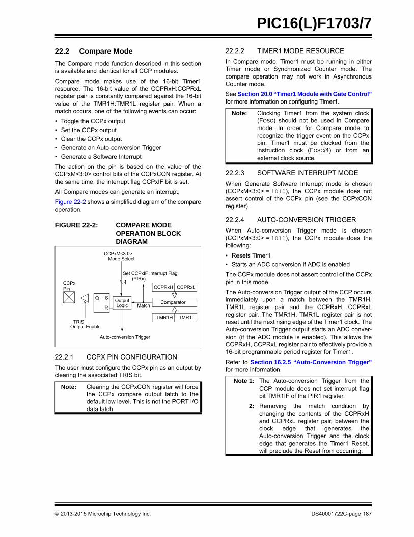
PIC16(L)F1703/7
22.2 Compare Mode
The Compare mode function described in this sectionis available and identical for all CCP modules.
Compare mode makes use of the 16-bit Timer1resource. The 16-bit value of the CCPRxH:CCPRxLregister pair is constantly compared against the 16-bitvalue of the TMR1H:TMR1L register pair. When amatch occurs, one of the following events can occur:
• Toggle the CCPx output
• Set the CCPx output
• Clear the CCPx output
• Generate an Auto-conversion Trigger
• Generate a Software Interrupt
The action on the pin is based on the value of theCCPxM<3:0> control bits of the CCPxCON register. Atthe same time, the interrupt flag CCPxIF bit is set.
All Compare modes can generate an interrupt.
Figure 22-2 shows a simplified diagram of the compareoperation.
FIGURE 22-2: COMPARE MODE OPERATION BLOCK DIAGRAM
22.2.1 CCPX PIN CONFIGURATION
The user must configure the CCPx pin as an output byclearing the associated TRIS bit.
22.2.2 TIMER1 MODE RESOURCE
In Compare mode, Timer1 must be running in eitherTimer mode or Synchronized Counter mode. Thecompare operation may not work in AsynchronousCounter mode.
See Section 20.0 “Timer1 Module with Gate Control”for more information on configuring Timer1.
22.2.3 SOFTWARE INTERRUPT MODE
When Generate Software Interrupt mode is chosen(CCPxM<3:0> = 1010), the CCPx module does notassert control of the CCPx pin (see the CCPxCONregister).
22.2.4 AUTO-CONVERSION TRIGGER
When Auto-conversion Trigger mode is chosen(CCPxM<3:0> = 1011), the CCPx module does thefollowing:
• Resets Timer1
• Starts an ADC conversion if ADC is enabled
The CCPx module does not assert control of the CCPxpin in this mode.
The Auto-conversion Trigger output of the CCP occursimmediately upon a match between the TMR1H,TMR1L register pair and the CCPRxH, CCPRxLregister pair. The TMR1H, TMR1L register pair is notreset until the next rising edge of the Timer1 clock. TheAuto-conversion Trigger output starts an ADC conver-sion (if the ADC module is enabled). This allows theCCPRxH, CCPRxL register pair to effectively provide a16-bit programmable period register for Timer1.
Refer to Section 16.2.5 “Auto-Conversion Trigger”for more information.
Note: Clearing the CCPxCON register will forcethe CCPx compare output latch to thedefault low level. This is not the PORT I/Odata latch.
CCPRxH CCPRxL
TMR1H TMR1L
ComparatorQ S
R
OutputLogic
Auto-conversion Trigger
Set CCPxIF Interrupt Flag(PIRx)
Match
TRIS
CCPxM<3:0>Mode Select
Output Enable
PinCCPx 4
Note: Clocking Timer1 from the system clock(FOSC) should not be used in Comparemode. In order for Compare mode torecognize the trigger event on the CCPxpin, TImer1 must be clocked from theinstruction clock (FOSC/4) or from anexternal clock source.
Note 1: The Auto-conversion Trigger from theCCP module does not set interrupt flagbit TMR1IF of the PIR1 register.
2: Removing the match condition bychanging the contents of the CCPRxHand CCPRxL register pair, between theclock edge that generates theAuto-conversion Trigger and the clockedge that generates the Timer1 Reset,will preclude the Reset from occurring.
2013-2015 Microchip Technology Inc. DS40001722C-page 187

PIC16(L)F1703/7
22.2.5 COMPARE DURING SLEEP
The Compare mode is dependent upon the systemclock (FOSC) for proper operation. Since FOSC is shutdown during Sleep mode, the Compare mode will notfunction properly during Sleep.
DS40001722C-page 188 2013-2015 Microchip Technology Inc.
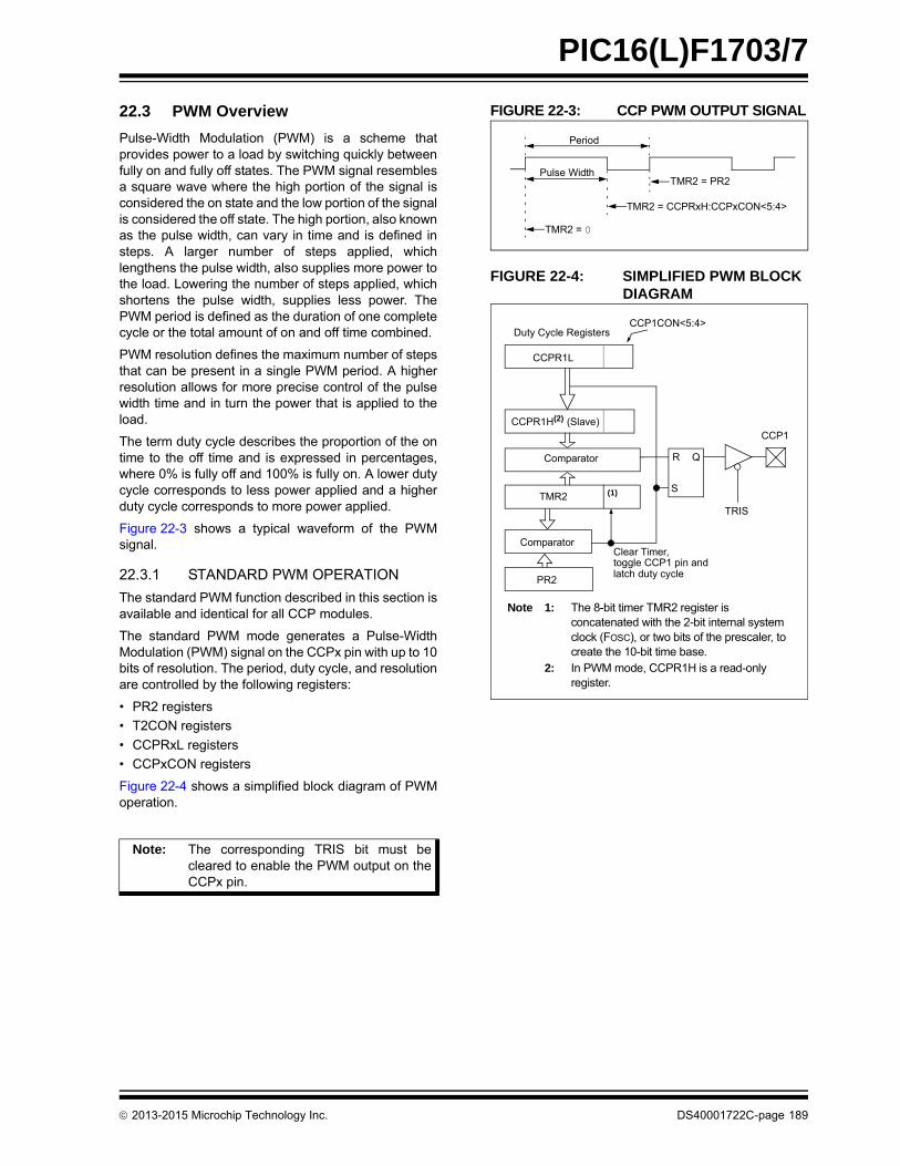
PIC16(L)F1703/7
22.3 PWM Overview
Pulse-Width Modulation (PWM) is a scheme thatprovides power to a load by switching quickly betweenfully on and fully off states. The PWM signal resemblesa square wave where the high portion of the signal isconsidered the on state and the low portion of the signalis considered the off state. The high portion, also knownas the pulse width, can vary in time and is defined insteps. A larger number of steps applied, whichlengthens the pulse width, also supplies more power tothe load. Lowering the number of steps applied, whichshortens the pulse width, supplies less power. ThePWM period is defined as the duration of one completecycle or the total amount of on and off time combined.
PWM resolution defines the maximum number of stepsthat can be present in a single PWM period. A higherresolution allows for more precise control of the pulsewidth time and in turn the power that is applied to theload.
The term duty cycle describes the proportion of the ontime to the off time and is expressed in percentages,where 0% is fully off and 100% is fully on. A lower dutycycle corresponds to less power applied and a higherduty cycle corresponds to more power applied.
Figure 22-3 shows a typical waveform of the PWMsignal.
22.3.1 STANDARD PWM OPERATION
The standard PWM function described in this section isavailable and identical for all CCP modules.
The standard PWM mode generates a Pulse-WidthModulation (PWM) signal on the CCPx pin with up to 10bits of resolution. The period, duty cycle, and resolutionare controlled by the following registers:
• PR2 registers
• T2CON registers
• CCPRxL registers
• CCPxCON registers
Figure 22-4 shows a simplified block diagram of PWMoperation.
FIGURE 22-3: CCP PWM OUTPUT SIGNAL
FIGURE 22-4: SIMPLIFIED PWM BLOCK DIAGRAM
Note: The corresponding TRIS bit must becleared to enable the PWM output on theCCPx pin.
Period
Pulse Width
TMR2 = 0
TMR2 = CCPRxH:CCPxCON<5:4>
TMR2 = PR2
CCPR1L
CCPR1H(2) (Slave)
Comparator
TMR2
PR2
(1)
R Q
S
Duty Cycle RegistersCCP1CON<5:4>
Clear Timer,toggle CCP1 pin and latch duty cycle
Note 1: The 8-bit timer TMR2 register is concatenated with the 2-bit internal system clock (FOSC), or two bits of the prescaler, to create the 10-bit time base.
2: In PWM mode, CCPR1H is a read-only register.
TRIS
CCP1
Comparator
2013-2015 Microchip Technology Inc. DS40001722C-page 189

PIC16(L)F1703/7
22.3.2 SETUP FOR PWM OPERATION
The following steps should be taken when configuringthe CCP module for standard PWM operation:
1. Use the desired output pin RxyPPS control toselect CCPx as the source and disable theCCPx pin output driver by setting the associatedTRIS bit.
2. Load the PR2 register with the PWM periodvalue.
3. Configure the CCP module for the PWM modeby loading the CCPxCON register with theappropriate values.
4. Load the CCPRxL register and the DCxBx bitsof the CCPxCON register, with the PWM dutycycle value.
5. Configure and start Timer2:
• Clear the TMR2IF interrupt flag bit of the PIRx register. See Note below.
• Configure the T2CKPS bits of the T2CON register with the Timer prescale value.
• Enable the Timer by setting the TMR2ON bit of the T2CON register.
6. Enable PWM output pin:
• Wait until the Timer overflows and the TMR2IF bit of the PIR1 register is set. See Note below.
• Enable the CCPx pin output driver by clearing the associated TRIS bit.
22.3.3 TIMER2 TIMER RESOURCE
The PWM standard mode makes use of the 8-bitTimer2 timer resources to specify the PWM period.
22.3.4 PWM PERIOD
The PWM period is specified by the PR2 register ofTimer2. The PWM period can be calculated using theformula of Equation 22-1.
EQUATION 22-1: PWM PERIOD
When TMR2 is equal to PR2, the following three eventsoccur on the next increment cycle:
• TMR2 is cleared
• The CCPx pin is set. (Exception: If the PWM duty cycle = 0%, the pin will not be set.)
• The PWM duty cycle is latched from CCPRxL into CCPRxH.
22.3.5 PWM DUTY CYCLE
The PWM duty cycle is specified by writing a 10-bitvalue to multiple registers: CCPRxL register andDCxB<1:0> bits of the CCPxCON register. TheCCPRxL contains the eight MSbs and the DCxB<1:0>bits of the CCPxCON register contain the two LSbs.CCPRxL and DCxB<1:0> bits of the CCPxCONregister can be written to at any time. The duty cyclevalue is not latched into CCPRxH until after the periodcompletes (i.e., a match between PR2 and TMR2registers occurs). While using the PWM, the CCPRxHregister is read-only.
Equation 22-2 is used to calculate the PWM pulsewidth.
Equation 22-3 is used to calculate the PWM duty cycleratio.
EQUATION 22-2: PULSE WIDTH
EQUATION 22-3: DUTY CYCLE RATIO
The CCPRxH register and a 2-bit internal latch areused to double buffer the PWM duty cycle. This doublebuffering is essential for glitchless PWM operation.
The 8-bit timer TMR2 register is concatenated witheither the 2-bit internal system clock (FOSC), or two bitsof the prescaler, to create the 10-bit time base. Thesystem clock is used if the Timer2 prescaler is set to 1:1.
When the 10-bit time base matches the CCPRxH and2-bit latch, then the CCPx pin is cleared (seeFigure 22-4).
Note: In order to send a complete duty cycle andperiod on the first PWM output, the abovesteps must be included in the setupsequence. If it is not critical to start with acomplete PWM signal on the first output,then step 6 may be ignored.
PWM Period PR2 1+ 4 TOSC =
(TMR2 Prescale Value)
Note 1: TOSC = 1/FOSC
Note: The Timer postscaler (see Section 21.1“Timer2 Operation”) is not used in thedetermination of the PWM frequency.
Pulse Width CCPRxL:CCPxCON<5:4> =
TOSC (TMR2 Prescale Value)
Duty Cycle RatioCCPRxL:CCPxCON<5:4>
4 PR2 1+ -----------------------------------------------------------------------=
DS40001722C-page 190 2013-2015 Microchip Technology Inc.
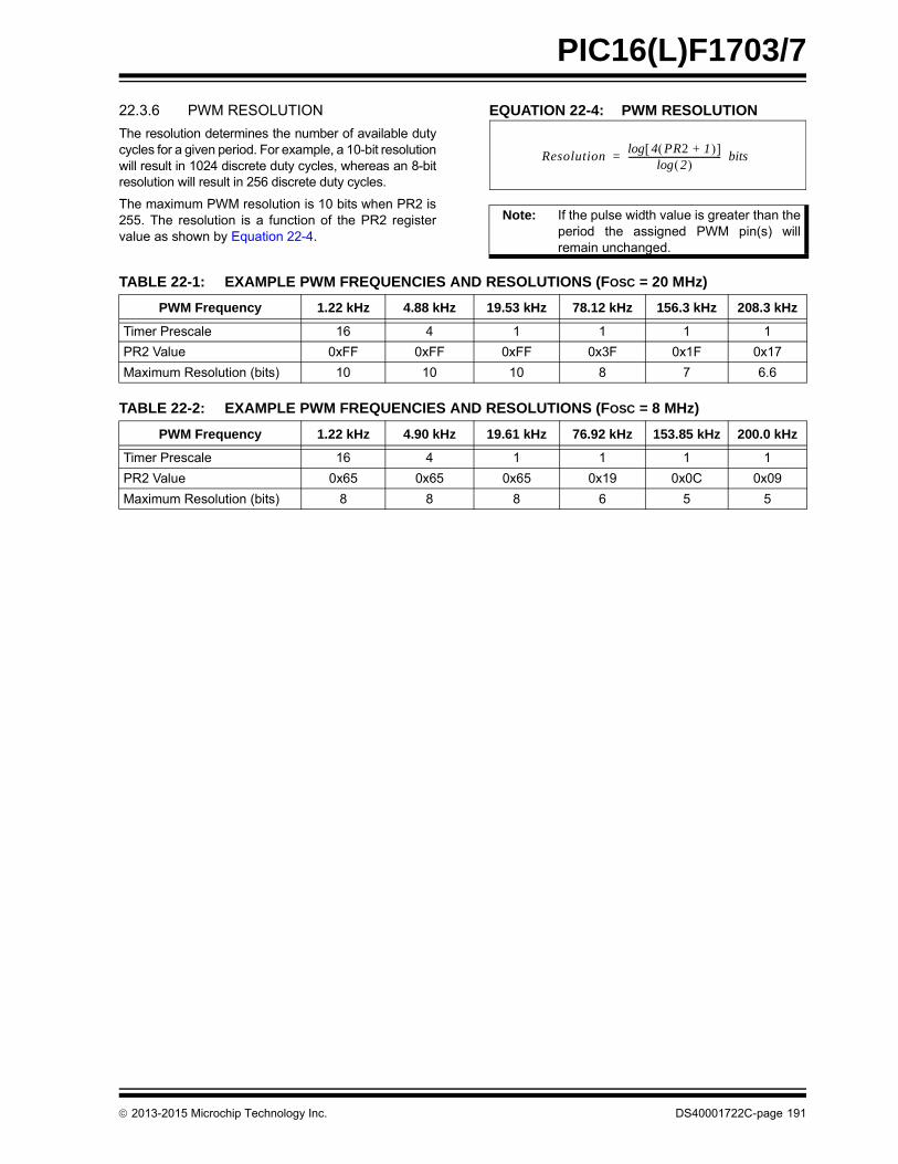
PIC16(L)F1703/7
22.3.6 PWM RESOLUTION
The resolution determines the number of available dutycycles for a given period. For example, a 10-bit resolutionwill result in 1024 discrete duty cycles, whereas an 8-bitresolution will result in 256 discrete duty cycles.
The maximum PWM resolution is 10 bits when PR2 is255. The resolution is a function of the PR2 registervalue as shown by Equation 22-4.
EQUATION 22-4: PWM RESOLUTION
TABLE 22-1: EXAMPLE PWM FREQUENCIES AND RESOLUTIONS (FOSC = 20 MHz)
TABLE 22-2: EXAMPLE PWM FREQUENCIES AND RESOLUTIONS (FOSC = 8 MHz)
Note: If the pulse width value is greater than theperiod the assigned PWM pin(s) willremain unchanged.
Resolution4 PR2 1+ log
2 log------------------------------------------ bits=
PWM Frequency 1.22 kHz 4.88 kHz 19.53 kHz 78.12 kHz 156.3 kHz 208.3 kHz
Timer Prescale 16 4 1 1 1 1
PR2 Value 0xFF 0xFF 0xFF 0x3F 0x1F 0x17
Maximum Resolution (bits) 10 10 10 8 7 6.6
PWM Frequency 1.22 kHz 4.90 kHz 19.61 kHz 76.92 kHz 153.85 kHz 200.0 kHz
Timer Prescale 16 4 1 1 1 1
PR2 Value 0x65 0x65 0x65 0x19 0x0C 0x09
Maximum Resolution (bits) 8 8 8 6 5 5
2013-2015 Microchip Technology Inc. DS40001722C-page 191

PIC16(L)F1703/7
22.3.7 OPERATION IN SLEEP MODE
In Sleep mode, the TMR2 register will not incrementand the state of the module will not change. If the CCPxpin is driving a value, it will continue to drive that value.When the device wakes up, TMR2 will continue from itsprevious state.
22.3.8 CHANGES IN SYSTEM CLOCK FREQUENCY
The PWM frequency is derived from the system clockfrequency. Any changes in the system clock frequencywill result in changes to the PWM frequency. SeeSection 6.0 “Oscillator Module (with Fail-SafeClock Monitor)” for additional details.
22.3.9 EFFECTS OF RESET
Any Reset will force all ports to Input mode and theCCP registers to their Reset states.
TABLE 22-3: SUMMARY OF REGISTERS ASSOCIATED WITH STANDARD PWM
Name Bit 7 Bit 6 Bit 5 Bit 4 Bit 3 Bit 2 Bit 1 Bit 0Register on Page
CCP1CON — — DC1B<1:0> CCP1M<3:0> 193
CCPR1L CCPR1L<7:0> 190*
INTCON GIE PEIE TMR0IE INTE IOCIE TMR0IF INTF IOCIF 77
PIE1 TMR1GIE ADIE — — SSP1IE CCP1IE TMR2IE TMR1IE 78
PIE2 — — — — BCL1IE — — CCP2IE 79
PIR1 TMR1GIF ADIF — — SSP1IF CCP1IF TMR2IF TMR1IF 81
PIR2 — — — — BCL1IF — — CCP2IF 82
PR2 PR2 180*
RxyPPS — — — RxyPPS<4:0> 132
T2CON — T2OUTPS<3:0> TMR2ON T2CKPS<1:0> 182
TMR2 TMR2 180
Legend: — = Unimplemented location, read as ‘0’. Shaded cells are not used by the PWM.* Page provides register information.
Note 1: Unimplemented, read as ‘1’.
DS40001722C-page 192 2013-2015 Microchip Technology Inc.
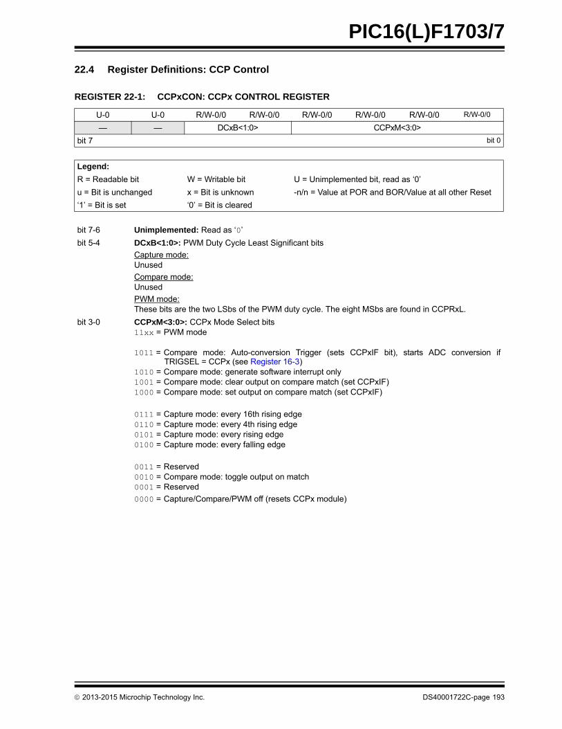
PIC16(L)F1703/7
22.4 Register Definitions: CCP Control
REGISTER 22-1: CCPxCON: CCPx CONTROL REGISTER
U-0 U-0 R/W-0/0 R/W-0/0 R/W-0/0 R/W-0/0 R/W-0/0 R/W-0/0
— — DCxB<1:0> CCPxM<3:0>
bit 7 bit 0
Legend:
R = Readable bit W = Writable bit U = Unimplemented bit, read as ‘0’
u = Bit is unchanged x = Bit is unknown -n/n = Value at POR and BOR/Value at all other Reset
‘1’ = Bit is set ‘0’ = Bit is cleared
bit 7-6 Unimplemented: Read as ‘0’
bit 5-4 DCxB<1:0>: PWM Duty Cycle Least Significant bits
Capture mode:Unused
Compare mode:Unused
PWM mode:These bits are the two LSbs of the PWM duty cycle. The eight MSbs are found in CCPRxL.
bit 3-0 CCPxM<3:0>: CCPx Mode Select bits11xx = PWM mode
1011 = Compare mode: Auto-conversion Trigger (sets CCPxIF bit), starts ADC conversion ifTRIGSEL = CCPx (see Register 16-3)
1010 = Compare mode: generate software interrupt only1001 = Compare mode: clear output on compare match (set CCPxIF)1000 = Compare mode: set output on compare match (set CCPxIF)
0111 = Capture mode: every 16th rising edge0110 = Capture mode: every 4th rising edge 0101 = Capture mode: every rising edge0100 = Capture mode: every falling edge
0011 = Reserved0010 = Compare mode: toggle output on match0001 = Reserved
0000 = Capture/Compare/PWM off (resets CCPx module)
2013-2015 Microchip Technology Inc. DS40001722C-page 193
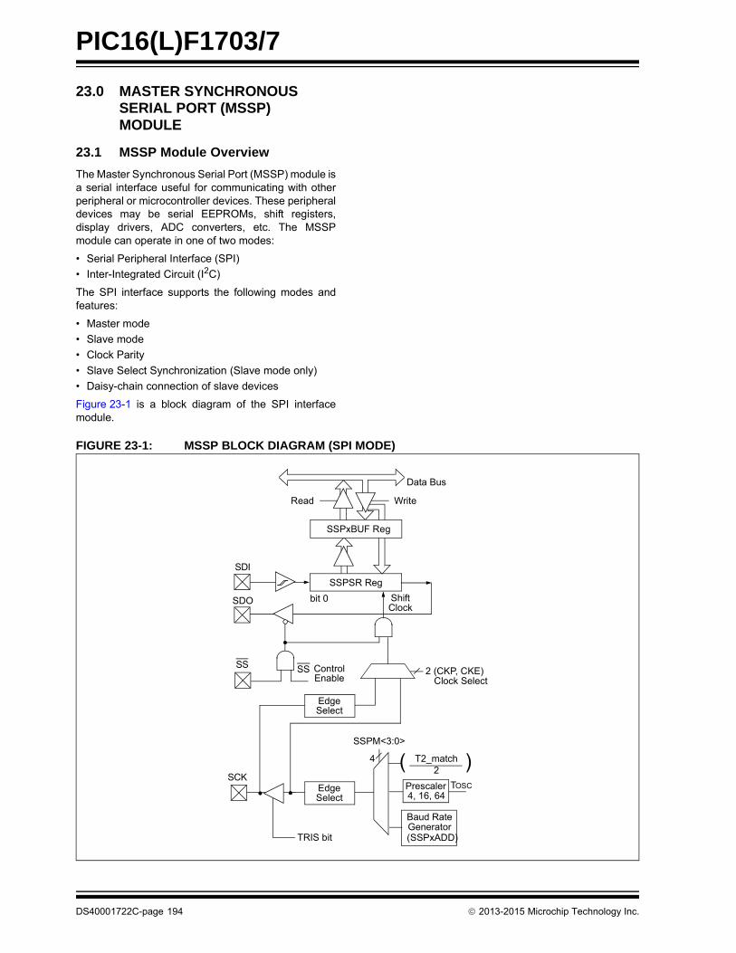
PIC16(L)F1703/7
23.0 MASTER SYNCHRONOUS SERIAL PORT (MSSP) MODULE
23.1 MSSP Module Overview
The Master Synchronous Serial Port (MSSP) module isa serial interface useful for communicating with otherperipheral or microcontroller devices. These peripheraldevices may be serial EEPROMs, shift registers,display drivers, ADC converters, etc. The MSSPmodule can operate in one of two modes:
• Serial Peripheral Interface (SPI)
• Inter-Integrated Circuit (I2C)
The SPI interface supports the following modes andfeatures:
• Master mode
• Slave mode
• Clock Parity
• Slave Select Synchronization (Slave mode only)
• Daisy-chain connection of slave devices
Figure 23-1 is a block diagram of the SPI interfacemodule.
FIGURE 23-1: MSSP BLOCK DIAGRAM (SPI MODE)
( )
Read Write
Data Bus
SSPSR Reg
SSPM<3:0>
bit 0 ShiftClock
SS ControlEnable
EdgeSelect
Clock Select
T2_match2
EdgeSelect
2 (CKP, CKE)
4
TRIS bit
SDO
SSPxBUF Reg
SDI
SS
SCKTOSCPrescaler
4, 16, 64
Baud RateGenerator(SSPxADD)
DS40001722C-page 194 2013-2015 Microchip Technology Inc.
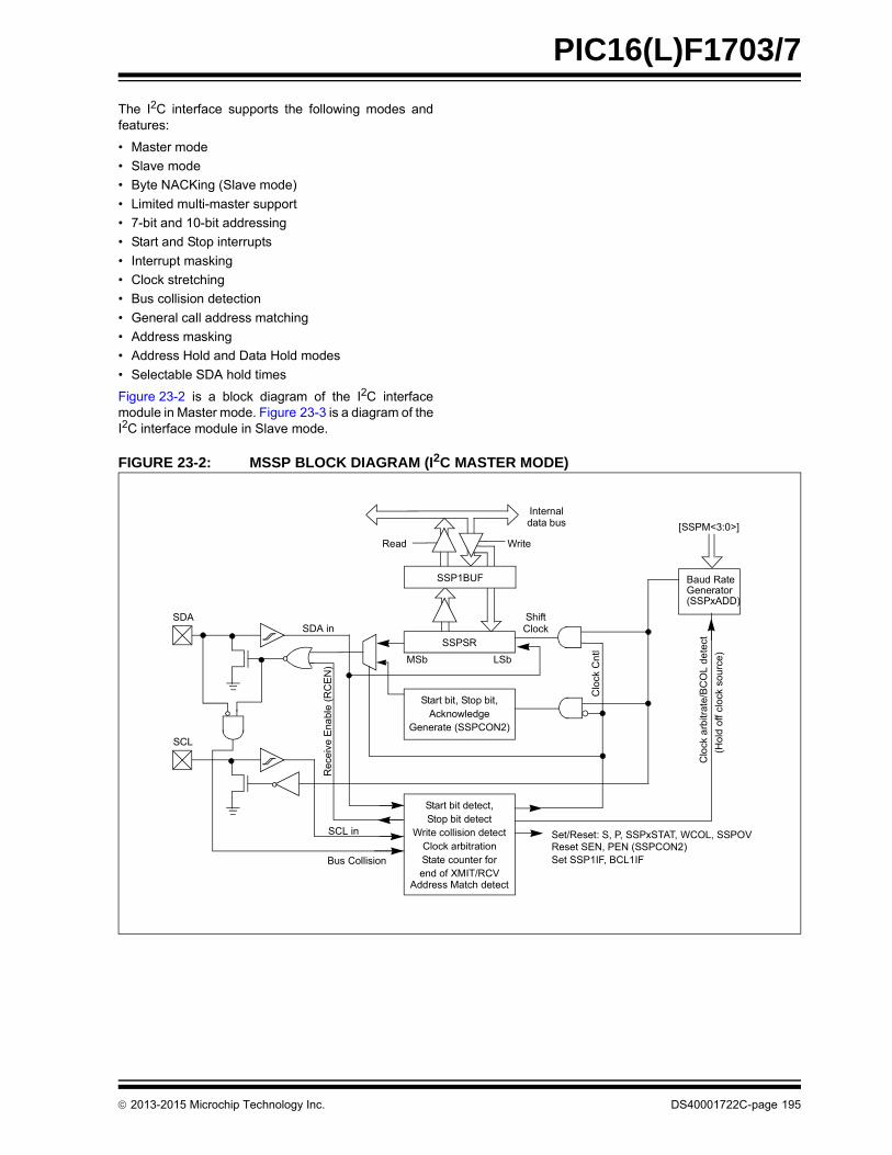
PIC16(L)F1703/7
The I2C interface supports the following modes andfeatures:
• Master mode
• Slave mode
• Byte NACKing (Slave mode)
• Limited multi-master support
• 7-bit and 10-bit addressing
• Start and Stop interrupts
• Interrupt masking
• Clock stretching
• Bus collision detection
• General call address matching
• Address masking
• Address Hold and Data Hold modes
• Selectable SDA hold times
Figure 23-2 is a block diagram of the I2C interfacemodule in Master mode. Figure 23-3 is a diagram of theI2C interface module in Slave mode.
FIGURE 23-2: MSSP BLOCK DIAGRAM (I2C MASTER MODE)
Read Write
SSPSR
Start bit, Stop bit,
Start bit detect,
SSP1BUF
Internaldata bus
Set/Reset: S, P, SSPxSTAT, WCOL, SSPOV
ShiftClock
MSb LSb
SDA
AcknowledgeGenerate (SSPCON2)
Stop bit detectWrite collision detect
Clock arbitrationState counter forend of XMIT/RCV
SCL
SCL in
Bus Collision
SDA in
Rec
eive
Ena
ble
(RC
EN
)
Clo
ck C
ntl
Clo
ck a
rbitr
ate/
BC
OL
de
tect
(Hol
d o
ff cl
ock
sou
rce
)
[SSPM<3:0>]
Baud Rate
Reset SEN, PEN (SSPCON2)
Generator(SSPxADD)
Address Match detect
Set SSP1IF, BCL1IF
2013-2015 Microchip Technology Inc. DS40001722C-page 195

PIC16(L)F1703/7
FIGURE 23-3: MSSP BLOCK DIAGRAM (I2C SLAVE MODE)
Read Write
SSPSR Reg
Match Detect
SSPxADD Reg
Start andStop bit Detect
SSPxBUF Reg
InternalData Bus
Addr Match
Set, ResetS, P bits
(SSPxSTAT Reg)
SCL
SDA
ShiftClock
MSb LSb
SSPMSK Reg
DS40001722C-page 196 2013-2015 Microchip Technology Inc.
PIC16(L)F1703/7
23.2 SPI Mode Overview
The Serial Peripheral Interface (SPI) bus is asynchronous serial data communication bus thatoperates in Full-Duplex mode. Devices communicatein a master/slave environment where the master deviceinitiates the communication. A slave device iscontrolled through a Chip Select known as SlaveSelect.
The SPI bus specifies four signal connections:
• Serial Clock (SCK)
• Serial Data Out (SDO)
• Serial Data In (SDI)
• Slave Select (SS)
Figure 23-1 shows the block diagram of the MSSPmodule when operating in SPI mode.
The SPI bus operates with a single master device andone or more slave devices. When multiple slavedevices are used, an independent Slave Selectconnection is required from the master device to eachslave device.
Figure 23-4 shows a typical connection between amaster device and multiple slave devices.
The master selects only one slave at a time. Most slavedevices have tri-state outputs so their output signalappears disconnected from the bus when they are notselected.
Transmissions involve two shift registers, eight bits insize, one in the master and one in the slave. With eitherthe master or the slave device, data is always shiftedout one bit at a time, with the Most Significant bit (MSb)shifted out first. At the same time, a new LeastSignificant bit (LSb) is shifted into the same register.
Figure 23-5 shows a typical connection between twoprocessors configured as master and slave devices.
Data is shifted out of both shift registers on theprogrammed clock edge and latched on the oppositeedge of the clock.
The master device transmits information out on its SDOoutput pin which is connected to, and received by, theslave’s SDI input pin. The slave device transmits infor-mation out on its SDO output pin, which is connectedto, and received by, the master’s SDI input pin.
To begin communication, the master device first sendsout the clock signal. Both the master and the slavedevices should be configured for the same clock polar-ity.
The master device starts a transmission by sending outthe MSb from its shift register. The slave device readsthis bit from that same line and saves it into the LSbposition of its shift register.
During each SPI clock cycle, a full-duplex datatransmission occurs. This means that while the masterdevice is sending out the MSb from its shift register (onits SDO pin) and the slave device is reading this bit andsaving it as the LSb of its shift register, that the slavedevice is also sending out the MSb from its shift register(on its SDO pin) and the master device is reading thisbit and saving it as the LSb of its shift register.
After eight bits have been shifted out, the master andslave have exchanged register values.
If there is more data to exchange, the shift registers areloaded with new data and the process repeats itself.
Whether the data is meaningful or not (dummy data),depends on the application software. This leads tothree scenarios for data transmission:
• Master sends useful data and slave sends dummy data.
• Master sends useful data and slave sends useful data.
• Master sends dummy data and slave sends useful data.
Transmissions may involve any number of clockcycles. When there is no more data to be transmitted,the master stops sending the clock signal and itdeselects the slave.
Every slave device connected to the bus that has notbeen selected through its slave select line must disre-gard the clock and transmission signals and must nottransmit out any data of its own.
2013-2015 Microchip Technology Inc. DS40001722C-page 197
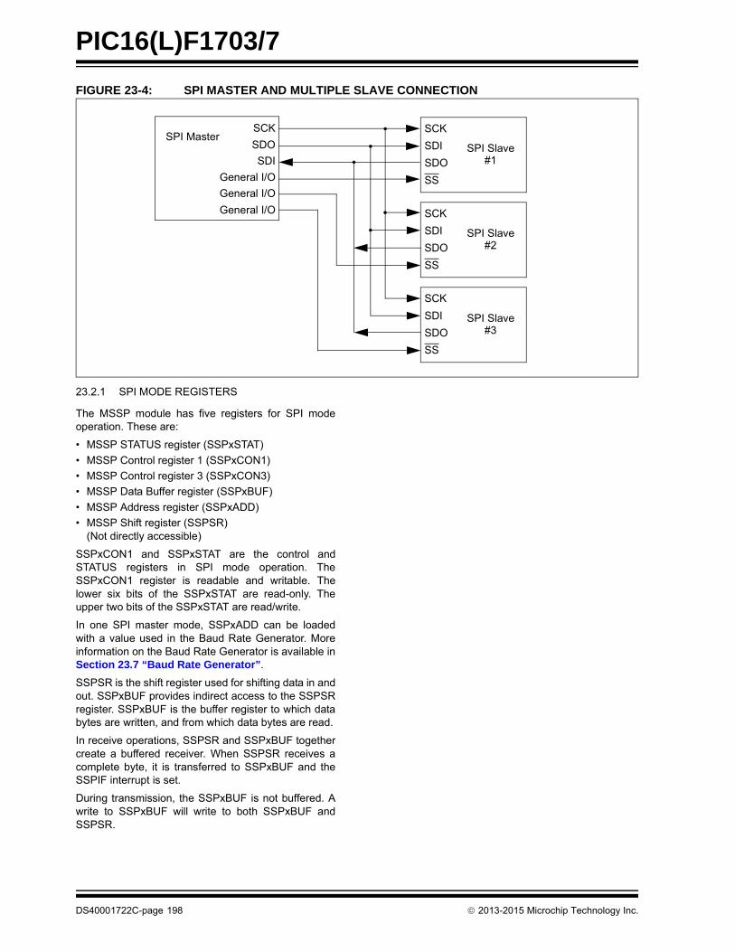
PIC16(L)F1703/7
FIGURE 23-4: SPI MASTER AND MULTIPLE SLAVE CONNECTION
23.2.1 SPI MODE REGISTERS
The MSSP module has five registers for SPI modeoperation. These are:
• MSSP STATUS register (SSPxSTAT)
• MSSP Control register 1 (SSPxCON1)
• MSSP Control register 3 (SSPxCON3)
• MSSP Data Buffer register (SSPxBUF)
• MSSP Address register (SSPxADD)
• MSSP Shift register (SSPSR) (Not directly accessible)
SSPxCON1 and SSPxSTAT are the control andSTATUS registers in SPI mode operation. TheSSPxCON1 register is readable and writable. Thelower six bits of the SSPxSTAT are read-only. Theupper two bits of the SSPxSTAT are read/write.
In one SPI master mode, SSPxADD can be loadedwith a value used in the Baud Rate Generator. Moreinformation on the Baud Rate Generator is available inSection 23.7 “Baud Rate Generator”.
SSPSR is the shift register used for shifting data in andout. SSPxBUF provides indirect access to the SSPSRregister. SSPxBUF is the buffer register to which databytes are written, and from which data bytes are read.
In receive operations, SSPSR and SSPxBUF togethercreate a buffered receiver. When SSPSR receives acomplete byte, it is transferred to SSPxBUF and theSSPIF interrupt is set.
During transmission, the SSPxBUF is not buffered. Awrite to SSPxBUF will write to both SSPxBUF andSSPSR.
SPI MasterSCK
SDO
SDI
General I/O
General I/O
General I/O
SCK
SDI
SDO
SS
SPI Slave#1
SCK
SDI
SDO
SS
SPI Slave#2
SCK
SDI
SDO
SS
SPI Slave#3
DS40001722C-page 198 2013-2015 Microchip Technology Inc.
PIC16(L)F1703/7
23.2.2 SPI MODE OPERATION
When initializing the SPI, several options need to bespecified. This is done by programming the appropriatecontrol bits (SSPxCON1<5:0> and SSPxSTAT<7:6>).These control bits allow the following to be specified:
• Master mode (SCK is the clock output)
• Slave mode (SCK is the clock input)
• Clock Polarity (Idle state of SCK)
• Data Input Sample Phase (middle or end of data output time)
• Clock Edge (output data on rising/falling edge of SCK)
• Clock Rate (Master mode only)
• Slave Select mode (Slave mode only)
To enable the serial port, SSP Enable bit, SSPEN of theSSPxCON1 register, must be set. To reset or reconfig-ure SPI mode, clear the SSPEN bit, re-initialize theSSPCONx registers and then set the SSPEN bit. Thisconfigures the SDI, SDO, SCK and SS pins as serialport pins. For the pins to behave as the serial portfunction, some must have their data direction bits (inthe TRIS register) appropriately programmed asfollows:
• SDI must have corresponding TRIS bit set
• SDO must have corresponding TRIS bit cleared
• SCK (Master mode) must have corresponding TRIS bit cleared
• SCK (Slave mode) must have corresponding TRIS bit set
• SS must have corresponding TRIS bit set
Any serial port function that is not desired may beoverridden by programming the corresponding datadirection (TRIS) register to the opposite value.
The MSSP consists of a transmit/receive shift register(SSPSR) and a buffer register (SSPxBUF). TheSSPSR shifts the data in and out of the device, MSbfirst. The SSPxBUF holds the data that was written tothe SSPSR until the received data is ready. Once theeight bits of data have been received, that byte ismoved to the SSPxBUF register. Then, the Buffer FullDetect bit, BF of the SSPxSTAT register, and the inter-rupt flag bit, SSPIF, are set. This double-buffering of thereceived data (SSPxBUF) allows the next byte to startreception before reading the data that was justreceived. Any write to the SSPxBUF register duringtransmission/reception of data will be ignored and thewrite collision detect bit WCOL of the SSPxCON1 reg-ister, will be set. User software must clear the WCOL bitto allow the following write(s) to the SSPxBUF registerto complete successfully.
When the application software is expecting to receivevalid data, the SSPxBUF should be read before thenext byte of data to transfer is written to the SSPxBUF.The Buffer Full bit, BF of the SSPxSTAT register,indicates when SSPxBUF has been loaded with thereceived data (transmission is complete). When theSSPxBUF is read, the BF bit is cleared. This data maybe irrelevant if the SPI is only a transmitter. Generally,the MSSP interrupt is used to determine when thetransmission/reception has completed. If the interruptmethod is not going to be used, then software pollingcan be done to ensure that a write collision does notoccur.
The SSPSR is not directly readable or writable and canonly be accessed by addressing the SSPxBUF register.Additionally, the SSPxSTAT register indicates thevarious Status conditions.
2013-2015 Microchip Technology Inc. DS40001722C-page 199
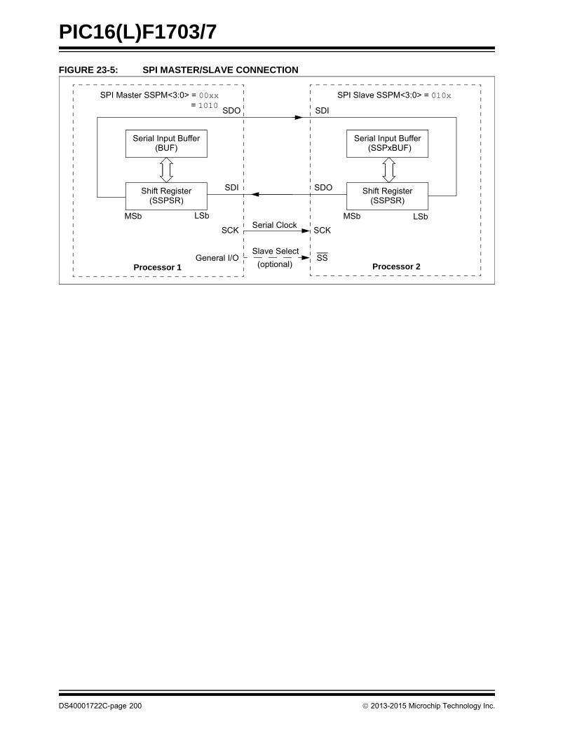
PIC16(L)F1703/7
FIGURE 23-5: SPI MASTER/SLAVE CONNECTION
Serial Input Buffer(BUF)
Shift Register(SSPSR)
MSb LSb
SDO
SDI
Processor 1
SCK
SPI Master SSPM<3:0> = 00xx
Serial Input Buffer(SSPxBUF)
Shift Register(SSPSR)
LSbMSb
SDI
SDO
Processor 2
SCK
SPI Slave SSPM<3:0> = 010x
Serial Clock
SSSlave Select
General I/O(optional)
= 1010
DS40001722C-page 200 2013-2015 Microchip Technology Inc.
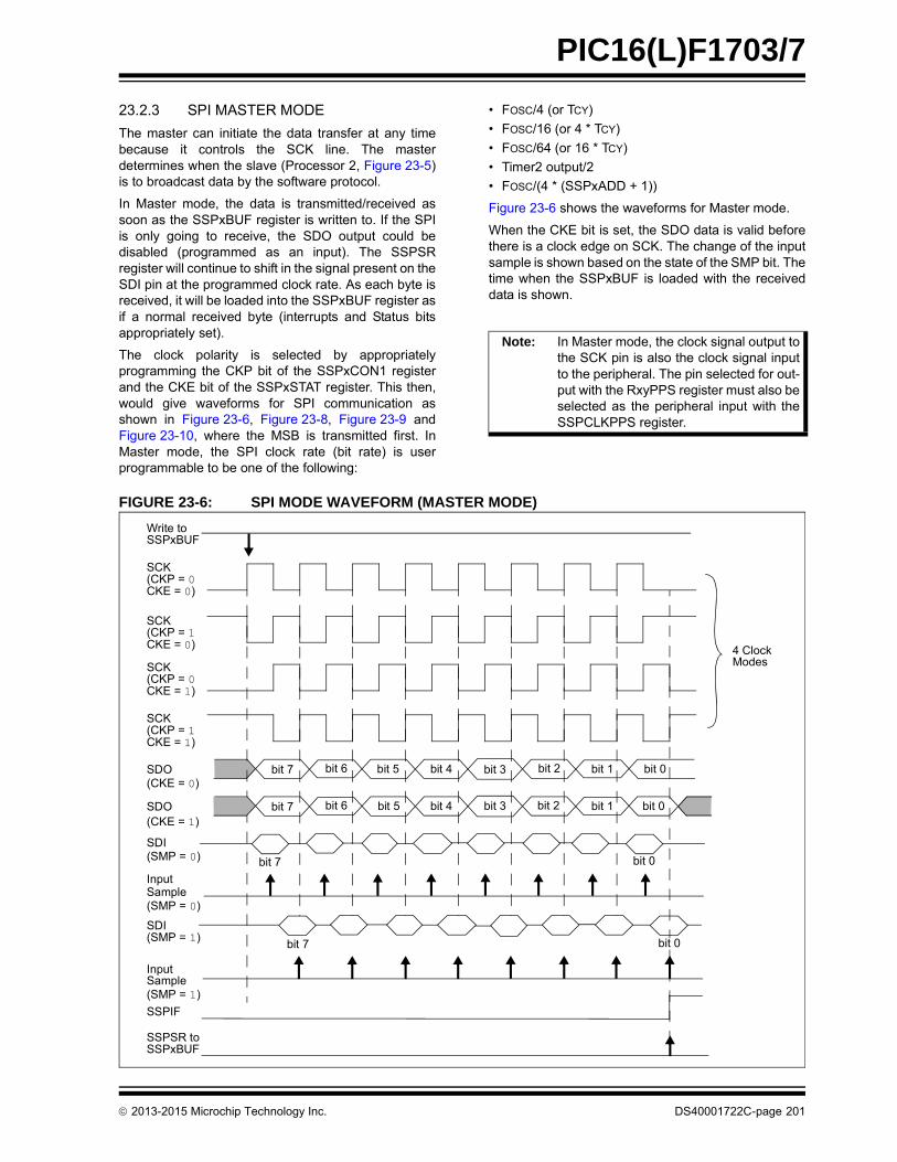
PIC16(L)F1703/7
23.2.3 SPI MASTER MODE
The master can initiate the data transfer at any timebecause it controls the SCK line. The masterdetermines when the slave (Processor 2, Figure 23-5)is to broadcast data by the software protocol.
In Master mode, the data is transmitted/received assoon as the SSPxBUF register is written to. If the SPIis only going to receive, the SDO output could bedisabled (programmed as an input). The SSPSRregister will continue to shift in the signal present on theSDI pin at the programmed clock rate. As each byte isreceived, it will be loaded into the SSPxBUF register asif a normal received byte (interrupts and Status bitsappropriately set).
The clock polarity is selected by appropriatelyprogramming the CKP bit of the SSPxCON1 registerand the CKE bit of the SSPxSTAT register. This then,would give waveforms for SPI communication asshown in Figure 23-6, Figure 23-8, Figure 23-9 andFigure 23-10, where the MSB is transmitted first. InMaster mode, the SPI clock rate (bit rate) is userprogrammable to be one of the following:
• FOSC/4 (or TCY)
• FOSC/16 (or 4 * TCY)
• FOSC/64 (or 16 * TCY)
• Timer2 output/2
• FOSC/(4 * (SSPxADD + 1))
Figure 23-6 shows the waveforms for Master mode.
When the CKE bit is set, the SDO data is valid beforethere is a clock edge on SCK. The change of the inputsample is shown based on the state of the SMP bit. Thetime when the SSPxBUF is loaded with the receiveddata is shown.
FIGURE 23-6: SPI MODE WAVEFORM (MASTER MODE)
Note: In Master mode, the clock signal output tothe SCK pin is also the clock signal inputto the peripheral. The pin selected for out-put with the RxyPPS register must also beselected as the peripheral input with theSSPCLKPPS register.
SCK(CKP = 0
SCK(CKP = 1
SCK(CKP = 0
SCK(CKP = 1
4 ClockModes
InputSample
InputSample
SDI
bit 7 bit 0
SDO bit 7 bit 6 bit 5 bit 4 bit 3 bit 2 bit 1 bit 0
bit 7
SDI
SSPIF
(SMP = 1)
(SMP = 0)
(SMP = 1)
CKE = 1)
CKE = 0)
CKE = 1)
CKE = 0)
(SMP = 0)
Write toSSPxBUF
SSPSR toSSPxBUF
SDO bit 7 bit 6 bit 5 bit 4 bit 3 bit 2 bit 1 bit 0
(CKE = 0)
(CKE = 1)
bit 0
2013-2015 Microchip Technology Inc. DS40001722C-page 201

PIC16(L)F1703/7
23.2.4 SPI SLAVE MODE
In Slave mode, the data is transmitted and received asexternal clock pulses appear on SCK. When the lastbit is latched, the SSPIF interrupt flag bit is set.
Before enabling the module in SPI Slave mode, the clockline must match the proper Idle state. The clock line canbe observed by reading the SCK pin. The Idle state isdetermined by the CKP bit of the SSPxCON1 register.
While in Slave mode, the external clock is supplied bythe external clock source on the SCK pin. This externalclock must meet the minimum high and low times asspecified in the electrical specifications.
While in Sleep mode, the slave can transmit/receivedata. The shift register is clocked from the SCK pininput and when a byte is received, the device willgenerate an interrupt. If enabled, the device willwake-up from Sleep.
23.2.4.1 Daisy-Chain Configuration
The SPI bus can sometimes be connected in adaisy-chain configuration. The first slave output isconnected to the second slave input, the second slaveoutput is connected to the third slave input, and so on.The final slave output is connected to the master input.Each slave sends out, during a second group of clockpulses, an exact copy of what was received during thefirst group of clock pulses. The whole chain acts asone large communication shift register. Thedaisy-chain feature only requires a single Slave Selectline from the master device.
Figure 23-7 shows the block diagram of a typicaldaisy-chain connection when operating in SPI mode.
In a daisy-chain configuration, only the most recentbyte on the bus is required by the slave. Setting theBOEN bit of the SSPxCON3 register will enable writesto the SSPxBUF register, even if the previous byte hasnot been read. This allows the software to ignore datathat may not apply to it.
23.2.5 SLAVE SELECT SYNCHRONIZATION
The Slave Select can also be used to synchronizecommunication. The Slave Select line is held high untilthe master device is ready to communicate. When theSlave Select line is pulled low, the slave knows that anew transmission is starting.
If the slave fails to receive the communication properly,it will be reset at the end of the transmission, when theSlave Select line returns to a high state. The slave isthen ready to receive a new transmission when theSlave Select line is pulled low again. If the Slave Selectline is not used, there is a risk that the slave willeventually become out of sync with the master. If theslave misses a bit, it will always be one bit off in futuretransmissions. Use of the Slave Select line allows theslave and master to align themselves at the beginningof each transmission.
The SS pin allows a Synchronous Slave mode. TheSPI must be in Slave mode with SS pin control enabled(SSPxCON1<3:0> = 0100).
When the SS pin is low, transmission and reception areenabled and the SDO pin is driven.
When the SS pin goes high, the SDO pin is no longerdriven, even if in the middle of a transmitted byte andbecomes a floating output. External pull-up/pull-downresistors may be desirable depending on the applica-tion.
When the SPI module resets, the bit counter is forcedto ‘0’. This can be done by either forcing the SS pin toa high level or clearing the SSPEN bit.
Note 1: When the SPI is in Slave mode with SS pincontrol enabled (SSPxCON1<3:0> =0100), the SPI module will reset if the SSpin is set to VDD.
2: When the SPI is used in Slave mode withCKE set; the user must enable SS pincontrol.
3: While operated in SPI Slave mode theSMP bit of the SSPxSTAT register mustremain clear.
DS40001722C-page 202 2013-2015 Microchip Technology Inc.

PIC16(L)F1703/7
FIGURE 23-7: SPI DAISY-CHAIN CONNECTION
FIGURE 23-8: SLAVE SELECT SYNCHRONOUS WAVEFORM
SPI MasterSCK
SDO
SDI
General I/O
SCK
SDI
SDO
SS
SPI Slave#1
SCK
SDI
SDO
SS
SPI Slave#2
SCK
SDI
SDO
SS
SPI Slave#3
SCK(CKP = 1
SCK(CKP = 0
InputSample
SDI
bit 7
SDO bit 7 bit 6 bit 7
SSPIFInterrupt
CKE = 0)
CKE = 0)
Write toSSPxBUF
SSPSR toSSPxBUF
SS
Flag
bit 0
bit 7
bit 0
bit 6
SSPxBUF toSSPSR
Shift register SSPSRand bit count are reset
2013-2015 Microchip Technology Inc. DS40001722C-page 203
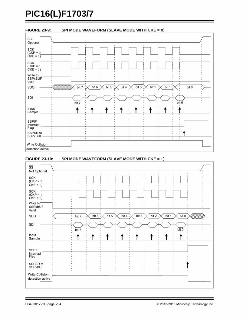
PIC16(L)F1703/7
FIGURE 23-9: SPI MODE WAVEFORM (SLAVE MODE WITH CKE = 0)
FIGURE 23-10: SPI MODE WAVEFORM (SLAVE MODE WITH CKE = 1)
SCK(CKP = 1
SCK(CKP = 0
InputSample
SDI
bit 7
SDO bit 7 bit 6 bit 5 bit 4 bit 3 bit 2 bit 1 bit 0
SSPIFInterrupt
CKE = 0)
CKE = 0)
Write toSSPxBUF
SSPSR toSSPxBUF
SS
Flag
Optional
bit 0
detection active
Write Collision
Valid
SCK(CKP = 1
SCK(CKP = 0
InputSample
SDI
bit 7 bit 0
SDO bit 7 bit 6 bit 5 bit 4 bit 3 bit 2 bit 1 bit 0
SSPIFInterrupt
CKE = 1)
CKE = 1)
Write toSSPxBUF
SSPSR toSSPxBUF
SS
Flag
Not Optional
Write Collisiondetection active
Valid
DS40001722C-page 204 2013-2015 Microchip Technology Inc.

PIC16(L)F1703/7
23.2.6 SPI OPERATION IN SLEEP MODE
In SPI Master mode, module clocks may be operatingat a different speed than when in Full-Power mode; inthe case of the Sleep mode, all clocks are halted.
Special care must be taken by the user when the MSSPclock is much faster than the system clock.
In Slave mode, when MSSP interrupts are enabled,after the master completes sending data, an MSSPinterrupt will wake the controller from Sleep.
If an exit from Sleep mode is not desired, MSSPinterrupts should be disabled.
In SPI Master mode, when the Sleep mode is selected,all module clocks are halted and the transmis-sion/reception will remain in that state until the devicewakes. After the device returns to Run mode, themodule will resume transmitting and receiving data.
In SPI Slave mode, the SPI Transmit/Receive Shiftregister operates asynchronously to the device. Thisallows the device to be placed in Sleep mode and datato be shifted into the SPI Transmit/Receive Shiftregister. When all eight bits have been received, theMSSP interrupt flag bit will be set and if enabled, willwake the device.
TABLE 23-1: SUMMARY OF REGISTERS ASSOCIATED WITH SPI OPERATION
Name Bit 7 Bit 6 Bit 5 Bit 4 Bit 3 Bit 2 Bit 1 Bit 0Register on Page
ANSELA — — — ANSA4 — ANSA2 ANSA1 ANSA0 114
ANSELC ANSC7(2) ANSC6(2) ANSC5(3) ANSC4(3) ANSC3 ANSC2 ANSC1 ANSC0 125
INTCON GIE PEIE TMR0IE INTE IOCIE TMR0IF INTF IOCIF 77
PIE1 TMR1GIE ADIE — — SSP1IE CCP1IE TMR2IE TMR1IE 78
PIR1 TMR1GIF ADIF — — SSP1IF CCP1IF TMR2IF TMR1IF 81
RxyPPS — — — RxyPPS<4:0> 132
SSPCLKPPS — — — SSPCLKPPS<4:0> 130, 131
SSPDATPPS — — — SSPDATPPS<4:0> 130, 131
SSPSSPPS — — — SSPSSPPS<4:0> 130, 131
SSP1BUF BUF<7:0> 198*
SSP1CON1 WCOL SSPOV SSPEN CKP SSPM<3:0> 244
SSP1CON3 ACKTIM PCIE SCIE BOEN SDAHT SBCDE AHEN DHEN 246
SSP1STAT SMP CKE D/A P S R/W UA BF 242
TRISA — — TRISA5 TRISA4 —(1) TRISA2 TRISA1 TRISA0 113
TRISB(2) TRISB7 TRISB6 TRISB5 TRISB4 — — — — 119
TRISC TRISC7(2) TRISC6(2) TRISC5 TRISC4 TRISC3 TRISC2 TRISC1 TRISC0 124
Legend: — = Unimplemented location, read as ‘0’. Shaded cells are not used by the MSSP in SPI mode.* Page provides register information.
Note 1: Unimplemented, read as ‘1’.2: PIC16(L)F1707 only.3: PIC16(L)F1703 only.
2013-2015 Microchip Technology Inc. DS40001722C-page 205

PIC16(L)F1703/7
23.3 I2C MODE OVERVIEW
The Inter-Integrated Circuit (I2C) bus is a multi-masterserial data communication bus. Devices communicatein a master/slave environment where the masterdevices initiate the communication. A slave device iscontrolled through addressing.
The I2C bus specifies two signal connections:
• Serial Clock (SCL)
• Serial Data (SDA)
Figure 23-11 shows the block diagram of the MSSPmodule when operating in I2C mode.
Both the SCL and SDA connections are bidirectionalopen-drain lines, each requiring pull-up resistors for thesupply voltage. Pulling the line to ground is considereda logical zero and letting the line float is considered alogical one.
Figure 23-11 shows a typical connection between twoprocessors configured as master and slave devices.
The I2C bus can operate with one or more masterdevices and one or more slave devices.
There are four potential modes of operation for a givendevice:
• Master Transmit mode(master is transmitting data to a slave)
• Master Receive mode(master is receiving data from a slave)
• Slave Transmit mode(slave is transmitting data to a master)
• Slave Receive mode(slave is receiving data from the master)
To begin communication, a master device starts out inMaster Transmit mode. The master device sends out aStart bit followed by the address byte of the slave itintends to communicate with. This is followed by asingle Read/Write bit, which determines whether themaster intends to transmit to or receive data from theslave device.
If the requested slave exists on the bus, it will respondwith an Acknowledge bit, otherwise known as an ACK.The master then continues in either Transmit mode orReceive mode and the slave continues in the comple-ment, either in Receive mode or Transmit mode,respectively.
A Start bit is indicated by a high-to-low transition of theSDA line while the SCL line is held high. Address anddata bytes are sent out, Most Significant bit (MSb) first.The Read/Write bit is sent out as a logical one when themaster intends to read data from the slave, and is sentout as a logical zero when it intends to write data to theslave.
FIGURE 23-11: I2C MASTER/SLAVE CONNECTION
The Acknowledge bit (ACK) is an active-low signal,which holds the SDA line low to indicate to the transmit-ter that the slave device has received the transmitteddata and is ready to receive more.
The transition of a data bit is always performed whilethe SCL line is held low. Transitions that occur while theSCL line is held high are used to indicate Start and Stopbits.
If the master intends to write to the slave, then it repeat-edly sends out a byte of data, with the slave respondingafter each byte with an ACK bit. In this example, themaster device is in Master Transmit mode and theslave is in Slave Receive mode.
If the master intends to read from the slave, then itrepeatedly receives a byte of data from the slave, andresponds after each byte with an ACK bit. In this exam-ple, the master device is in Master Receive mode andthe slave is Slave Transmit mode.
On the last byte of data communicated, the masterdevice may end the transmission by sending a Stop bit.If the master device is in Receive mode, it sends theStop bit in place of the last ACK bit. A Stop bit isindicated by a low-to-high transition of the SDA linewhile the SCL line is held high.
In some cases, the master may want to maintaincontrol of the bus and re-initiate another transmission.If so, the master device may send another Start bit inplace of the Stop bit or last ACK bit when it is in receivemode.
The I2C bus specifies three message protocols;
• Single message where a master writes data to a slave.
• Single message where a master reads data from a slave.
• Combined message where a master initiates a minimum of two writes, or two reads, or a combination of writes and reads, to one or more slaves.
Master
SCL
SDA
SCL
SDA
SlaveVDD
VDD
DS40001722C-page 206 2013-2015 Microchip Technology Inc.
PIC16(L)F1703/7
When one device is transmitting a logical one, or lettingthe line float, and a second device is transmitting a log-ical zero, or holding the line low, the first device candetect that the line is not a logical one. This detection,when used on the SCL line, is called clock stretching.Clock stretching gives slave devices a mechanism tocontrol the flow of data. When this detection is used onthe SDA line, it is called arbitration. Arbitration ensuresthat there is only one master device communicating atany single time.
23.3.1 CLOCK STRETCHING
When a slave device has not completed processingdata, it can delay the transfer of more data through theprocess of clock stretching. An addressed slave devicemay hold the SCL clock line low after receiving or send-ing a bit, indicating that it is not yet ready to continue.The master that is communicating with the slave willattempt to raise the SCL line in order to transfer thenext bit, but will detect that the clock line has not yetbeen released. Because the SCL connection isopen-drain, the slave has the ability to hold that line lowuntil it is ready to continue communicating.
Clock stretching allows receivers that cannot keep upwith a transmitter to control the flow of incoming data.
23.3.2 ARBITRATION
Each master device must monitor the bus for Start andStop bits. If the device detects that the bus is busy, itcannot begin a new message until the bus returns to anIdle state.
However, two master devices may try to initiate a trans-mission on or about the same time. When this occurs,the process of arbitration begins. Each transmitterchecks the level of the SDA data line and compares itto the level that it expects to find. The first transmitter toobserve that the two levels do not match, loses arbitra-tion, and must stop transmitting on the SDA line.
For example, if one transmitter holds the SDA line to alogical one (lets it float) and a second transmitter holdsit to a logical zero (pulls it low), the result is that theSDA line will be low. The first transmitter then observesthat the level of the line is different than expected andconcludes that another transmitter is communicating.
The first transmitter to notice this difference is the onethat loses arbitration and must stop driving the SDAline. If this transmitter is also a master device, it alsomust stop driving the SCL line. It then can monitor thelines for a Stop condition before trying to reissue itstransmission. In the meantime, the other device thathas not noticed any difference between the expectedand actual levels on the SDA line continues with itsoriginal transmission. It can do so without any compli-cations, because so far, the transmission appearsexactly as expected with no other transmitter disturbingthe message.
Slave Transmit mode can also be arbitrated, when amaster addresses multiple slaves, but this is lesscommon.
If two master devices are sending a message to twodifferent slave devices at the address stage, the mastersending the lower slave address always wins arbitra-tion. When two master devices send messages to thesame slave address, and addresses can sometimesrefer to multiple slaves, the arbitration process mustcontinue into the data stage.
Arbitration usually occurs very rarely, but it is anecessary process for proper multi-master support.
2013-2015 Microchip Technology Inc. DS40001722C-page 207
PIC16(L)F1703/7
23.4 I2C MODE OPERATION
All MSSP I2C communication is byte oriented andshifted out MSb first. Six SFR registers and twointerrupt flags interface the module with the PIC®
microcontroller and user software. Two pins, SDA andSCL, are exercised by the module to communicatewith other external I2C devices.
23.4.1 BYTE FORMAT
All communication in I2C is done in 9-bit segments. Abyte is sent from a master to a slave or vice-versa, fol-lowed by an Acknowledge bit sent back. After theeighth falling edge of the SCL line, the device output-ting data on the SDA changes that pin to an input andreads in an acknowledge value on the next clockpulse.
The clock signal, SCL, is provided by the master. Datais valid to change while the SCL signal is low, andsampled on the rising edge of the clock. Changes onthe SDA line while the SCL line is high define specialconditions on the bus, explained below.
23.4.2 DEFINITION OF I2C TERMINOLOGY
There is language and terminology in the descriptionof I2C communication that have definitions specific toI2C. That word usage is defined below and may beused in the rest of this document without explanation.This table was adapted from the Philips I2Cspecification.
23.4.3 SDA AND SCL PINS
Selection of any I2C mode with the SSPEN bit set,forces the SCL and SDA pins to be open-drain. Thesepins should be set by the user to inputs by setting theappropriate TRIS bits.
23.4.4 SDA HOLD TIME
The hold time of the SDA pin is selected by the SDAHTbit of the SSPxCON3 register. Hold time is the timeSDA is held valid after the falling edge of SCL. Settingthe SDAHT bit selects a longer 300 ns minimum holdtime and may help on buses with large capacitance.
TABLE 23-2: I2C BUS TERMS
Note 1: Data is tied to output zero when an I2Cmode is enabled.
2: Any device pin can be selected for SDAand SCL functions with the PPS peripheral.These functions are bidirectional. The SDAinput is selected with the SSPDATPPSregisters. The SCL input is selected withthe SSPCLKPPS registers. Outputs areselected with the RxyPPS registers. It is theuser’s responsibility to make the selectionsso that both the input and the output foreach function is on the same pin.
TERM Description
Transmitter The device which shifts data out onto the bus.
Receiver The device which shifts data in from the bus.
Master The device that initiates a transfer, generates clock signals and termi-nates a transfer.
Slave The device addressed by the master.
Multi-master A bus with more than one device that can initiate data transfers.
Arbitration Procedure to ensure that only one master at a time controls the bus. Winning arbitration ensures that the message is not corrupted.
Synchronization Procedure to synchronize the clocks of two or more devices on the bus.
Idle No master is controlling the bus, and both SDA and SCL lines are high.
Active Any time one or more master devices are controlling the bus.
Addressed Slave
Slave device that has received a matching address and is actively being clocked by a master.
Matching Address
Address byte that is clocked into a slave that matches the value stored in SSPxADD.
Write Request Slave receives a matching address with R/W bit clear, and is ready to clock in data.
Read Request Master sends an address byte with the R/W bit set, indicating that it wishes to clock data out of the Slave. This data is the next and all following bytes until a Restart or Stop.
Clock Stretching When a device on the bus hold SCL low to stall communication.
Bus Collision Any time the SDA line is sampled low by the module while it is out-putting and expected high state.
DS40001722C-page 208 2013-2015 Microchip Technology Inc.
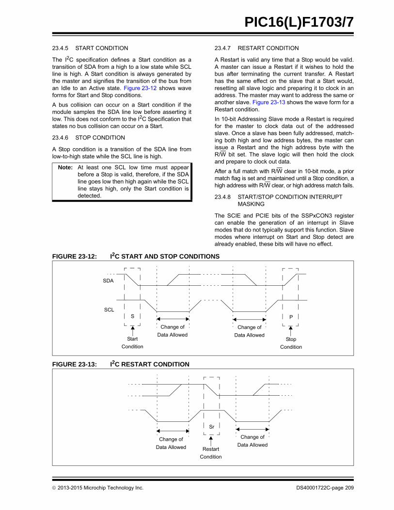
PIC16(L)F1703/7
23.4.5 START CONDITION
The I2C specification defines a Start condition as atransition of SDA from a high to a low state while SCLline is high. A Start condition is always generated bythe master and signifies the transition of the bus froman Idle to an Active state. Figure 23-12 shows waveforms for Start and Stop conditions.
A bus collision can occur on a Start condition if themodule samples the SDA line low before asserting itlow. This does not conform to the I2C Specification thatstates no bus collision can occur on a Start.
23.4.6 STOP CONDITION
A Stop condition is a transition of the SDA line fromlow-to-high state while the SCL line is high.
23.4.7 RESTART CONDITION
A Restart is valid any time that a Stop would be valid.A master can issue a Restart if it wishes to hold thebus after terminating the current transfer. A Restarthas the same effect on the slave that a Start would,resetting all slave logic and preparing it to clock in anaddress. The master may want to address the same oranother slave. Figure 23-13 shows the wave form for aRestart condition.
In 10-bit Addressing Slave mode a Restart is requiredfor the master to clock data out of the addressedslave. Once a slave has been fully addressed, match-ing both high and low address bytes, the master canissue a Restart and the high address byte with theR/W bit set. The slave logic will then hold the clockand prepare to clock out data.
After a full match with R/W clear in 10-bit mode, a priormatch flag is set and maintained until a Stop condition, ahigh address with R/W clear, or high address match fails.
23.4.8 START/STOP CONDITION INTERRUPT MASKING
The SCIE and PCIE bits of the SSPxCON3 registercan enable the generation of an interrupt in Slavemodes that do not typically support this function. Slavemodes where interrupt on Start and Stop detect arealready enabled, these bits will have no effect.
FIGURE 23-12: I2C START AND STOP CONDITIONS
FIGURE 23-13: I2C RESTART CONDITION
Note: At least one SCL low time must appearbefore a Stop is valid, therefore, if the SDAline goes low then high again while the SCLline stays high, only the Start condition isdetected.
SDA
SCL
P
Stop
Condition
S
Start
Condition
Change of
Data Allowed
Change of
Data Allowed
Restart
Condition
Sr
Change of
Data AllowedChange of
Data Allowed
2013-2015 Microchip Technology Inc. DS40001722C-page 209
PIC16(L)F1703/7
23.4.9 ACKNOWLEDGE SEQUENCE
The ninth SCL pulse for any transferred byte in I2C isdedicated as an Acknowledge. It allows receivingdevices to respond back to the transmitter by pullingthe SDA line low. The transmitter must release controlof the line during this time to shift in the response. TheAcknowledge (ACK) is an active-low signal, pulling theSDA line low indicates to the transmitter that thedevice has received the transmitted data and is readyto receive more.
The result of an ACK is placed in the ACKSTAT bit ofthe SSPCON2 register.
Slave software, when the AHEN and DHEN bits areset, allow the user to set the ACK value sent back tothe transmitter. The ACKDT bit of the SSPCON2 regis-ter is set/cleared to determine the response.
Slave hardware will generate an ACK response if theAHEN and DHEN bits of the SSPxCON3 register areclear.
There are certain conditions where an ACK will not besent by the slave. If the BF bit of the SSPxSTAT regis-ter or the SSPOV bit of the SSPxCON1 register areset when a byte is received.
When the module is addressed, after the eighth fallingedge of SCL on the bus, the ACKTIM bit of theSSPxCON3 register is set. The ACKTIM bit indicatesthe acknowledge time of the active bus. The ACKTIMStatus bit is only active when the AHEN bit or DHENbit is enabled.
23.5 I2C SLAVE MODE OPERATION
The MSSP Slave mode operates in one of four modesselected by the SSPM bits of SSPxCON1 register. Themodes can be divided into 7-bit and 10-bit Addressingmode. 10-bit Addressing modes operate the same as7-bit with some additional overhead for handling thelarger addresses.
Modes with Start and Stop bit interrupts operate thesame as the other modes with SSPIF additionallygetting set upon detection of a Start, Restart, or Stopcondition.
23.5.1 SLAVE MODE ADDRESSES
The SSPxADD register (Register 23-6) contains theSlave mode address. The first byte received after aStart or Restart condition is compared against thevalue stored in this register. If the byte matches, thevalue is loaded into the SSPxBUF register and aninterrupt is generated. If the value does not match, themodule goes idle and no indication is given to thesoftware that anything happened.
The SSP Mask register (Register 23-5) affects theaddress matching process. See Section 23.5.9 “SSPMask Register” for more information.
23.5.1.1 I2C Slave 7-bit Addressing Mode
In 7-bit Addressing mode, the LSb of the received databyte is ignored when determining if there is an addressmatch.
23.5.1.2 I2C Slave 10-bit Addressing Mode
In 10-bit Addressing mode, the first received byte iscompared to the binary value of ‘1 1 1 1 0 A9 A8 0’. A9and A8 are the two MSb’s of the 10-bit address andstored in bits 2 and 1 of the SSPxADD register.
After the acknowledge of the high byte the UA bit is setand SCL is held low until the user updates SSPxADDwith the low address. The low address byte is clockedin and all eight bits are compared to the low addressvalue in SSPxADD. Even if there is not an addressmatch; SSPIF and UA are set, and SCL is held lowuntil SSPxADD is updated to receive a high byteagain. When SSPxADD is updated the UA bit iscleared. This ensures the module is ready to receivethe high address byte on the next communication.
A high and low address match as a write request isrequired at the start of all 10-bit addressing communi-cation. A transmission can be initiated by issuing aRestart once the slave is addressed, and clocking inthe high address with the R/W bit set. The slavehardware will then acknowledge the read request andprepare to clock out data. This is only valid for a slaveafter it has received a complete high and low addressbyte match.
DS40001722C-page 210 2013-2015 Microchip Technology Inc.
PIC16(L)F1703/7
23.5.2 SLAVE RECEPTION
When the R/W bit of a matching received address byteis clear, the R/W bit of the SSPxSTAT register iscleared. The received address is loaded into theSSPxBUF register and acknowledged.
When the overflow condition exists for a receivedaddress, then not Acknowledge is given. An overflowcondition is defined as either bit BF of the SSPxSTATregister is set, or bit SSPOV of the SSPxCON1 registeris set. The BOEN bit of the SSPxCON3 register modi-fies this operation. For more information seeRegister 23-4.
An MSSP interrupt is generated for each transferreddata byte. Flag bit, SSPIF, must be cleared by software.
When the SEN bit of the SSPCON2 register is set, SCLwill be held low (clock stretch) following each receivedbyte. The clock must be released by setting the CKPbit of the SSPxCON1 register, except sometimes in10-bit mode. See Section 23.5.6.2 “10-bitAddressing Mode” for more detail.
23.5.2.1 7-bit Addressing Reception
This section describes a standard sequence of eventsfor the MSSP module configured as an I2C slave in7-bit Addressing mode. Figure 23-14 and Figure 23-15is used as a visual reference for this description.
This is a step by step process of what typically mustbe done to accomplish I2C communication.
1. Start bit detected.
2. S bit of SSPxSTAT is set; SSPIF is set if interrupton Start detect is enabled.
3. Matching address with R/W bit clear is received.
4. The slave pulls SDA low sending an ACK to themaster, and sets SSPIF bit.
5. Software clears the SSPIF bit.
6. Software reads received address fromSSPxBUF clearing the BF flag.
7. If SEN = 1; Slave software sets CKP bit torelease the SCL line.
8. The master clocks out a data byte.
9. Slave drives SDA low sending an ACK to themaster, and sets SSPIF bit.
10. Software clears SSPIF.
11. Software reads the received byte fromSSPxBUF clearing BF.
12. Steps 8-12 are repeated for all received bytesfrom the master.
13. Master sends Stop condition, setting P bit ofSSPxSTAT, and the bus goes idle.
23.5.2.2 7-bit Reception with AHEN and DHEN
Slave device reception with AHEN and DHEN setoperate the same as without these options with extrainterrupts and clock stretching added after the eighthfalling edge of SCL. These additional interrupts allowthe slave software to decide whether it wants to ACKthe receive address or data byte, rather than the hard-ware. This functionality adds support for PMBus™ thatwas not present on previous versions of this module.
This list describes the steps that need to be taken byslave software to use these options for I2C communi-cation. Figure 23-16 displays a module using bothaddress and data holding. Figure 23-17 includes theoperation with the SEN bit of the SSPCON2 registerset.
1. S bit of SSPxSTAT is set; SSPIF is set if interrupton Start detect is enabled.
2. Matching address with R/W bit clear is clockedin. SSPIF is set and CKP cleared after the eighthfalling edge of SCL.
3. Slave clears the SSPIF.
4. Slave can look at the ACKTIM bit of theSSPxCON3 register to determine if the SSPIFwas after or before the ACK.
5. Slave reads the address value from SSPxBUF,clearing the BF flag.
6. Slave sets ACK value clocked out to the masterby setting ACKDT.
7. Slave releases the clock by setting CKP.
8. SSPIF is set after an ACK, not after a NACK.
9. If SEN = 1 the slave hardware will stretch theclock after the ACK.
10. Slave clears SSPIF.
11. SSPIF set and CKP cleared after eighth fallingedge of SCL for a received data byte.
12. Slave looks at ACKTIM bit of SSPxCON3 todetermine the source of the interrupt.
13. Slave reads the received data from SSPxBUFclearing BF.
14. Steps 7-14 are the same for each received databyte.
15. Communication is ended by either the slavesending an ACK = 1, or the master sending aStop condition. If a Stop is sent and Interrupt onStop Detect is disabled, the slave will only knowby polling the P bit of the SSTSTAT register.
Note: SSPIF is still set after the ninth falling edgeof SCL even if there is no clock stretchingand BF has been cleared. Only if NACK issent to master is SSPIF not set
2013-2015 Microchip Technology Inc. DS40001722C-page 211

PIC16(L)F1703/7
FIGURE 23-14: I2C SLAVE, 7-BIT ADDRESS, RECEPTION (SEN = 0, AHEN = 0, DHEN = 0)
Rec
eivi
ng
Ad
dre
ss
AC
K
Rec
eiv
ing
Dat
a
AC
K
Rec
eiv
ing
Dat
aA
CK
=1
A7
A6
A5
A4
A3
A2
A1
D7
D6
D5
D4
D3
D2
D1
D0
D7
D6
D5
D4
D3
D2
D1
D0
SD
A
SC
L
SS
PIF
BF
SS
PO
V
12
34
56
78
12
34
56
78
12
34
56
78
99
9
AC
K is
no
t se
nt.
SS
PO
V s
et b
ecau
seS
SP
xBU
F is
stil
l fu
ll.
Cle
are
d b
y so
ftwar
e
Firs
t by
te o
f da
ta is
ava
ilabl
e in
SS
PxB
UF
SS
PxB
UF
is r
ead
SS
PIF
set
on
9th
falli
ng e
dge
of
SC
LC
lea
red
by s
oftw
are
P
Bu
s M
ast
er
send
s S
top
cond
ition
S
Fro
m S
lave
to M
aste
r
DS40001722C-page 212 2013-2015 Microchip Technology Inc.
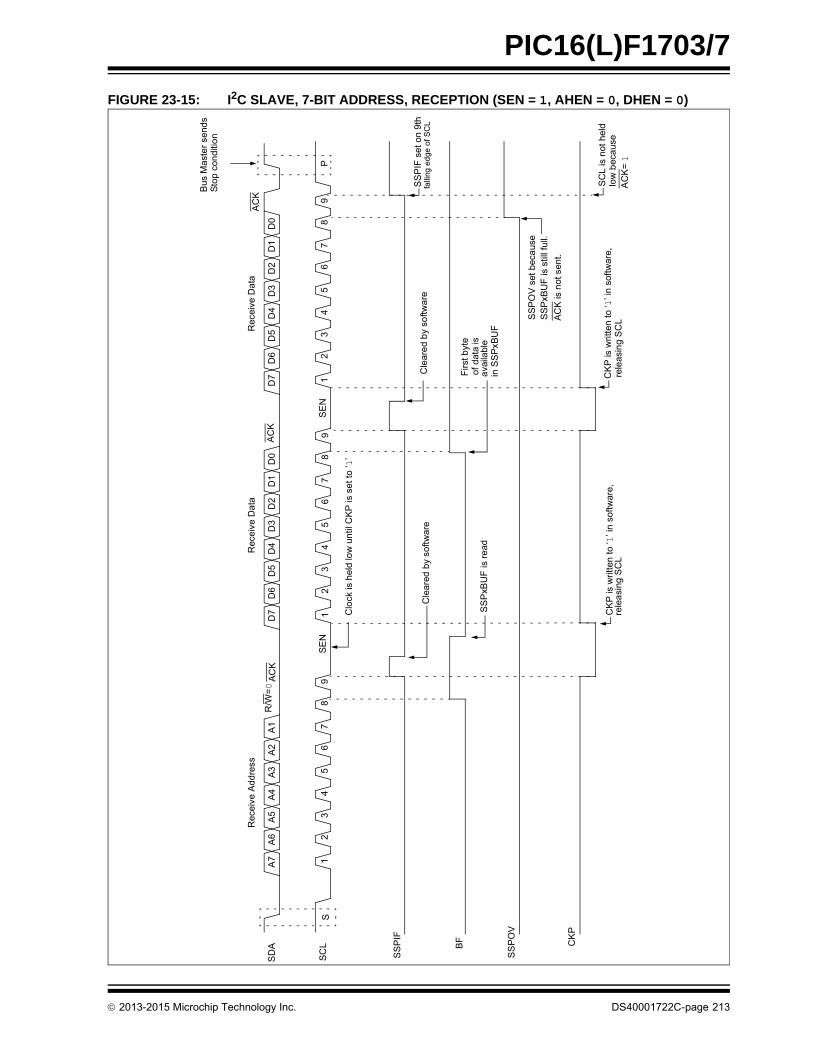
PIC16(L)F1703/7
FIGURE 23-15: I2C SLAVE, 7-BIT ADDRESS, RECEPTION (SEN = 1, AHEN = 0, DHEN = 0)
SE
NS
EN
A7
A6
A5
A4
A3
A2
A1
D7
D6
D5
D4
D3
D2
D1
D0
D7
D6
D5
D4
D3
D2
D1
D0
SD
A
SC
L1
23
45
67
89
12
34
56
78
91
23
45
67
89
P
SS
PIF
set
on
9th
SC
L is
not
hel
dC
KP
is w
ritte
n to
‘1’ i
n s
oftw
are,
C
KP
is w
ritte
n to
‘1’ i
n s
oftw
are,
AC
K
low
bec
aus
e
falli
ng e
dge
of
SC
L
rele
asin
g S
CL A
CK
is n
ot s
ent.
Bus
Mas
ter
send
s
CK
P
SS
PO
V
BF
SS
PIF
SS
PO
V s
et b
eca
use
SS
PxB
UF
is s
till f
ull.
Cle
are
d b
y so
ftwa
re
Firs
t byt
e o
f da
ta is
ava
ilabl
e in
SS
PxB
UF
AC
K=1
Cle
ared
by
softw
are
SS
PxB
UF
is r
ead
Clo
ck is
hel
d lo
w u
ntil
CK
P is
se
t to
‘1’
rele
asi
ng S
CL
Sto
p c
ondi
tion
S
AC
K
AC
KR
ecei
ve A
ddre
ssR
ecei
ve D
ata
Rec
eive
Dat
a
R/W
=0
2013-2015 Microchip Technology Inc. DS40001722C-page 213
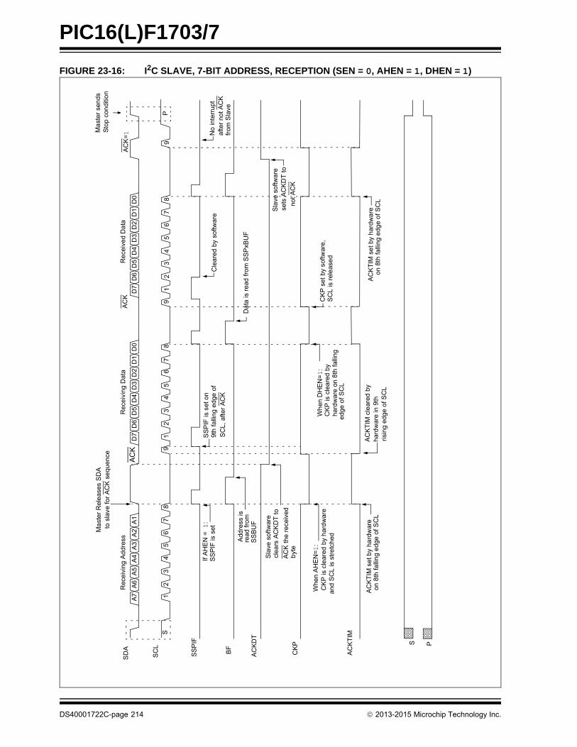
PIC16(L)F1703/7
FIGURE 23-16: I2C SLAVE, 7-BIT ADDRESS, RECEPTION (SEN = 0, AHEN = 1, DHEN = 1)
Rec
eiv
ing
Add
ress
Rec
eiv
ing
Dat
aR
ece
ive
d D
ata
P
A7
A6
A5
A4
A3
A2
A1
D7
D6
D5
D4
D3
D2
D1
D0
D7
D6
D5
D4
D3
D2
D1
D0
SD
A
SC
L
BF
CK
P S P
12
34
56
78
91
23
45
67
89
12
34
56
78
Ma
ster
sen
dsS
top
con
ditio
n
S
Da
ta is
re
ad f
rom
SS
PxB
UF
Cle
are
d b
y so
ftwar
eS
SP
IF is
set
on
9th
falli
ng
edg
e o
f S
CL,
afte
r A
CK
CK
P s
et b
y so
ftwar
e,
SC
L is
rel
eas
ed
Sla
ve s
oftw
are
9
AC
KT
IM c
lear
ed b
yh
ard
war
e in
9th
ri
sing
edg
e o
f SC
L
sets
AC
KD
T to
not
AC
K
Wh
en D
HE
N=1
:C
KP
is c
lea
red
by
hard
wa
re o
n 8
th f
allin
ge
dge
of
SC
L
Sla
ve s
oftw
are
clea
rs A
CK
DT
to
AC
K t
he r
ecei
ved
byt
e
AC
KT
IM s
et b
y ha
rdw
are
on 8
th fa
llin
g e
dge
of
SC
L
Whe
n A
HE
N=1
:C
KP
is c
lear
ed b
y h
ard
war
ean
d S
CL
is s
tre
tch
edAdd
ress
isre
ad fr
om
S
SB
UF
AC
KT
IM s
et b
y ha
rdw
are
on 8
th fa
lling
edg
e o
f SC
L
AC
K
Ma
ster
Rel
eas
es S
DA
to s
lave
for
AC
K s
equ
enc
e
No
inte
rru
pta
fter
not A
CK
from
Sla
ve
AC
K=1
AC
K
AC
KD
T
AC
KT
IM
SS
PIF
If A
HE
N=1
:S
SP
IF is
set
DS40001722C-page 214 2013-2015 Microchip Technology Inc.
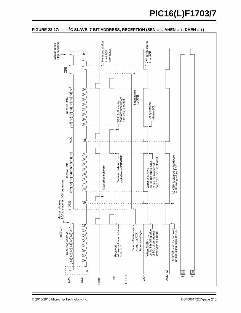
PIC16(L)F1703/7
FIGURE 23-17: I2C SLAVE, 7-BIT ADDRESS, RECEPTION (SEN = 1, AHEN = 1, DHEN = 1)
Re
ceiv
ing
Add
ress
Rec
eive
Da
taR
ece
ive
Dat
a
A7
A6
A5
A4
A3
A2
A1
D7
D6
D5
D4
D3
D2
D1
D0
D7
D6
D5
D4
D3
D2
D1
D0
SD
A
SC
L
SS
PIF B
F
AC
KD
T
CK
P S P
AC
K
S1
23
45
67
89
12
34
56
78
91
23
45
67
89
AC
K
AC
K
Cle
are
d b
y so
ftwar
e
AC
KT
IM is
cle
are
d b
y ha
rdw
are
SS
PxB
UF
can
be
Set
by
softw
are
,
rea
d a
ny ti
me
bef
ore
nex
t by
te is
load
ed
rele
ase
SC
L
on 9
th r
isin
g e
dge
of
SC
L
Re
ceiv
ed
add
ress
is lo
ade
d in
to
SS
PxB
UF
Sla
ve s
oftw
are
cle
ars
AC
KD
T t
o A
CK
R/W
= 0
Mas
ter
rele
ases
SD
A to
sla
ve fo
r A
CK
seq
uenc
e
the
re
ceiv
ed
byt
e
Whe
n A
HE
N=1
;on
the
8th
falli
ng
edg
eof
SC
L o
f an
add
ress
byte
, CK
P is
cle
are
d
AC
KT
IM is
set
by
har
dwar
eon
8th
fal
ling
ed
ge o
f SC
L
Whe
n D
HE
N =
1;
on t
he 8
th fa
llin
g e
dge
of S
CL
of
a re
ceiv
edda
ta b
yte,
CK
P is
cle
are
d
Re
ceiv
ed
dat
a is
ava
ilabl
e o
n S
SP
xBU
F
Sla
ve s
end
sn
ot A
CK
CK
P is
not
cle
are
dif
not A
CK
P
Ma
ster
sen
dsS
top
con
ditio
n
No
inte
rru
pt a
fter
if no
t AC
Kfr
om S
lave
AC
KT
IM
2013-2015 Microchip Technology Inc. DS40001722C-page 215
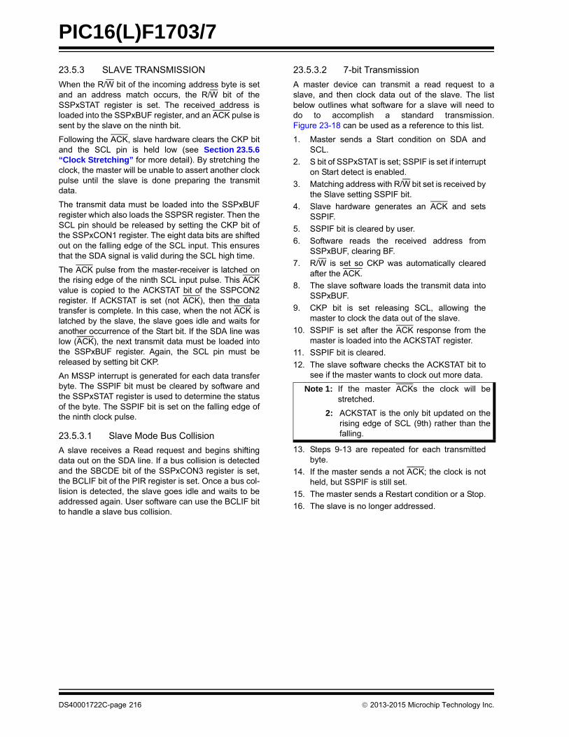
PIC16(L)F1703/7
23.5.3 SLAVE TRANSMISSION
When the R/W bit of the incoming address byte is setand an address match occurs, the R/W bit of theSSPxSTAT register is set. The received address isloaded into the SSPxBUF register, and an ACK pulse issent by the slave on the ninth bit.
Following the ACK, slave hardware clears the CKP bitand the SCL pin is held low (see Section 23.5.6“Clock Stretching” for more detail). By stretching theclock, the master will be unable to assert another clockpulse until the slave is done preparing the transmitdata.
The transmit data must be loaded into the SSPxBUFregister which also loads the SSPSR register. Then theSCL pin should be released by setting the CKP bit ofthe SSPxCON1 register. The eight data bits are shiftedout on the falling edge of the SCL input. This ensuresthat the SDA signal is valid during the SCL high time.
The ACK pulse from the master-receiver is latched onthe rising edge of the ninth SCL input pulse. This ACKvalue is copied to the ACKSTAT bit of the SSPCON2register. If ACKSTAT is set (not ACK), then the datatransfer is complete. In this case, when the not ACK islatched by the slave, the slave goes idle and waits foranother occurrence of the Start bit. If the SDA line waslow (ACK), the next transmit data must be loaded intothe SSPxBUF register. Again, the SCL pin must bereleased by setting bit CKP.
An MSSP interrupt is generated for each data transferbyte. The SSPIF bit must be cleared by software andthe SSPxSTAT register is used to determine the statusof the byte. The SSPIF bit is set on the falling edge ofthe ninth clock pulse.
23.5.3.1 Slave Mode Bus Collision
A slave receives a Read request and begins shiftingdata out on the SDA line. If a bus collision is detectedand the SBCDE bit of the SSPxCON3 register is set,the BCLIF bit of the PIR register is set. Once a bus col-lision is detected, the slave goes idle and waits to beaddressed again. User software can use the BCLIF bitto handle a slave bus collision.
23.5.3.2 7-bit Transmission
A master device can transmit a read request to aslave, and then clock data out of the slave. The listbelow outlines what software for a slave will need todo to accomplish a standard transmission.Figure 23-18 can be used as a reference to this list.
1. Master sends a Start condition on SDA andSCL.
2. S bit of SSPxSTAT is set; SSPIF is set if interrupton Start detect is enabled.
3. Matching address with R/W bit set is received bythe Slave setting SSPIF bit.
4. Slave hardware generates an ACK and setsSSPIF.
5. SSPIF bit is cleared by user.
6. Software reads the received address fromSSPxBUF, clearing BF.
7. R/W is set so CKP was automatically clearedafter the ACK.
8. The slave software loads the transmit data intoSSPxBUF.
9. CKP bit is set releasing SCL, allowing themaster to clock the data out of the slave.
10. SSPIF is set after the ACK response from themaster is loaded into the ACKSTAT register.
11. SSPIF bit is cleared.
12. The slave software checks the ACKSTAT bit tosee if the master wants to clock out more data.
13. Steps 9-13 are repeated for each transmittedbyte.
14. If the master sends a not ACK; the clock is notheld, but SSPIF is still set.
15. The master sends a Restart condition or a Stop.
16. The slave is no longer addressed.
Note 1: If the master ACKs the clock will bestretched.
2: ACKSTAT is the only bit updated on therising edge of SCL (9th) rather than thefalling.
DS40001722C-page 216 2013-2015 Microchip Technology Inc.
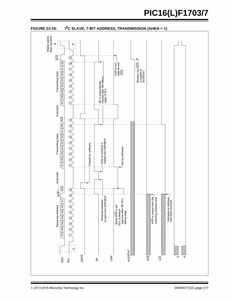
PIC16(L)F1703/7
FIGURE 23-18: I2C SLAVE, 7-BIT ADDRESS, TRANSMISSION (AHEN = 0)
Rec
eivi
ng A
ddre
ssA
uto
mat
icT
rans
mitt
ing
Da
taA
uto
ma
ticT
ran
smitt
ing
Dat
a
A7
A6
A5
A4
A3
A2
A1
D7
D6
D5
D4
D3
D2
D1
D0
D7
D6
D5
D4
D3
D2
D1
D0
12
34
56
78
91
23
45
67
89
12
34
56
78
9
SD
A
SC
L
SS
PIF
BF
CK
P
AC
KS
TA
T
R/W
D/A S P
Re
ceiv
ed
add
ress
Wh
en R
/W is
se
t
R/W
is c
opie
d fr
om th
e
Ind
icat
es
an a
ddr
ess
is r
ead
from
SS
PxB
UF
SC
L is
alw
ays
held
low
aft
er 9
th S
CL
falli
ng
edg
e
mat
chin
g a
ddr
ess
byt
e
has
been
re
ceiv
ed
Mas
ters
not
AC
Kis
cop
ied
to
AC
KS
TA
T
CK
P is
not
h
eld
for
not
AC
K
BF
is a
uto
ma
tical
ly
clea
red
aft
er 8
th f
allin
ged
ge o
f S
CL
Dat
a to
tra
nsm
it is
load
ed in
to S
SP
xBU
F
Se
t by
soft
war
e
Cle
are
d b
y so
ftw
are
AC
KA
CK
AC
KR
/W=1
SP
Mas
ter
send
sS
top
con
ditio
n
2013-2015 Microchip Technology Inc. DS40001722C-page 217
PIC16(L)F1703/7
23.5.3.3 7-bit Transmission with Address Hold Enabled
Setting the AHEN bit of the SSPxCON3 registerenables additional clock stretching and interruptgeneration after the eighth falling edge of a receivedmatching address. Once a matching address hasbeen clocked in, CKP is cleared and the SSPIFinterrupt is set.
Figure 23-19 displays a standard waveform of a 7-bitaddress slave transmission with AHEN enabled.
1. Bus starts Idle.
2. Master sends Start condition; the S bit ofSSPxSTAT is set; SSPIF is set if interrupt onStart detect is enabled.
3. Master sends matching address with R/W bitset. After the eighth falling edge of the SCL linethe CKP bit is cleared and SSPIF interrupt isgenerated.
4. Slave software clears SSPIF.
5. Slave software reads ACKTIM bit of SSPxCON3register, and R/W and D/A of the SSPxSTATregister to determine the source of the interrupt.
6. Slave reads the address value from theSSPxBUF register clearing the BF bit.
7. Slave software decides from this information if itwishes to ACK or not ACK and sets the ACKDTbit of the SSPCON2 register accordingly.
8. Slave sets the CKP bit releasing SCL.
9. Master clocks in the ACK value from the slave.
10. Slave hardware automatically clears the CKP bitand sets SSPIF after the ACK if the R/W bit isset.
11. Slave software clears SSPIF.
12. Slave loads value to transmit to the master intoSSPxBUF setting the BF bit.
13. Slave sets the CKP bit releasing the clock.
14. Master clocks out the data from the slave andsends an ACK value on the ninth SCL pulse.
15. Slave hardware copies the ACK value into theACKSTAT bit of the SSPCON2 register.
16. Steps 10-15 are repeated for each byte transmit-ted to the master from the slave.
17. If the master sends a not ACK the slavereleases the bus allowing the master to send aStop and end the communication.
Note: SSPxBUF cannot be loaded until after theACK.
Note: Master must send a not ACK on the lastbyte to ensure that the slave releases theSCL line to receive a Stop.
DS40001722C-page 218 2013-2015 Microchip Technology Inc.
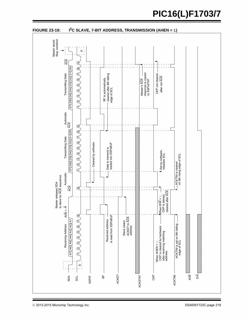
PIC16(L)F1703/7
FIGURE 23-19: I2C SLAVE, 7-BIT ADDRESS, TRANSMISSION (AHEN = 1)
Rec
eiv
ing
Ad
dres
sA
utom
atic
Tra
nsm
ittin
g D
ata
Aut
oma
ticT
rans
mitt
ing
Da
ta
A7
A6
A5
A4
A3
A2
A1
D7
D6
D5
D4
D3
D2
D1
D0
D7
D6
D5
D4
D3
D2
D1
D0
12
34
56
78
91
23
45
67
89
12
34
56
78
9
SD
A
SC
L
SS
PIF BF
AC
KD
T
AC
KS
TAT
CK
P
R/W D/A
Rec
eiv
ed a
ddr
ess
is r
ead
from
SS
PxB
UF
BF
is a
utom
atic
ally
cl
eare
d a
fter
8th
falli
ng
edg
e o
f S
CL
Dat
a to
tra
nsm
it is
loa
ded
into
SS
PxB
UF
Cle
ared
by
softw
are
Sla
ve c
lea
rs
AC
KD
T t
o A
CK
addr
ess
Ma
ster
’s A
CK
resp
onse
is c
opie
dto
SS
PxS
TAT
CK
P n
ot c
lear
ed
afte
r no
t A
CK
Se
t by
softw
are,
rele
ase
s S
CL
AC
KT
IM is
cle
ared
on
9th
risi
ng e
dge
of S
CL
AC
KT
IM is
set
on
8th
fal
ling
edg
e of
SC
L
Whe
n A
HE
N =
1;
CK
P is
cle
ared
by
har
dwar
eaf
ter
rece
ivin
g m
atch
ing
add
ress
.
Whe
n R
/W =
1;
CK
P is
alw
ays
clea
red
afte
r A
CK
SP
Mas
ter
send
sS
top
cond
ition
AC
KR
/W=1M
ast
er r
ele
ases
SD
Ato
sla
ve f
or A
CK
seq
uen
ce
AC
KA
CK
AC
KT
IM
2013-2015 Microchip Technology Inc. DS40001722C-page 219

PIC16(L)F1703/7
23.5.4 SLAVE MODE 10-BIT ADDRESS RECEPTION
This section describes a standard sequence of eventsfor the MSSP module configured as an I2C slave in10-bit Addressing mode.
Figure 23-20 is used as a visual reference for thisdescription.
This is a step by step process of what must be done byslave software to accomplish I2C communication.
1. Bus starts Idle.
2. Master sends Start condition; S bit of SSPxSTATis set; SSPIF is set if interrupt on Start detect isenabled.
3. Master sends matching high address with R/Wbit clear; UA bit of the SSPxSTAT register is set.
4. Slave sends ACK and SSPIF is set.
5. Software clears the SSPIF bit.
6. Software reads received address fromSSPxBUF clearing the BF flag.
7. Slave loads low address into SSPxADD,releasing SCL.
8. Master sends matching low address byte to theslave; UA bit is set.
9. Slave sends ACK and SSPIF is set.
10. Slave clears SSPIF.
11. Slave reads the received matching addressfrom SSPxBUF clearing BF.
12. Slave loads high address into SSPxADD.
13. Master clocks a data byte to the slave andclocks out the slaves ACK on the ninth SCLpulse; SSPIF is set.
14. If SEN bit of SSPCON2 is set, CKP is cleared byhardware and the clock is stretched.
15. Slave clears SSPIF.
16. Slave reads the received byte from SSPxBUFclearing BF.
17. If SEN is set the slave sets CKP to release theSCL.
18. Steps 13-17 repeat for each received byte.
19. Master sends Stop to end the transmission.
23.5.5 10-BIT ADDRESSING WITH ADDRESS OR DATA HOLD
Reception using 10-bit addressing with AHEN orDHEN set is the same as with 7-bit modes. The onlydifference is the need to update the SSPxADD registerusing the UA bit. All functionality, specifically when theCKP bit is cleared and SCL line is held low are thesame. Figure 23-21 can be used as a reference of aslave in 10-bit addressing with AHEN set.
Figure 23-22 shows a standard waveform for a slavetransmitter in 10-bit Addressing mode.
Note: Updates to the SSPxADD register are notallowed until after the ACK sequence.
Note: If the low address does not match, SSPIFand UA are still set so that the slave soft-ware can set SSPxADD back to the highaddress. BF is not set because there is nomatch. CKP is unaffected.
DS40001722C-page 220 2013-2015 Microchip Technology Inc.
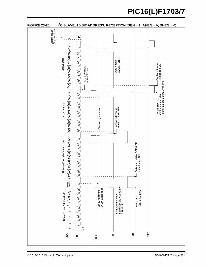
PIC16(L)F1703/7
FIGURE 23-20: I2C SLAVE, 10-BIT ADDRESS, RECEPTION (SEN = 1, AHEN = 0, DHEN = 0)
SS
PIF
Rec
eive
Firs
t Add
ress
Byt
e
AC
K
Rec
eive
Sec
ond
Add
ress
Byt
e AC
K
Rec
eive
Dat
a
AC
K
Rec
eive
Dat
a
AC
K1
11
10
A9
A8
A7
A6
A5
A4
A3
A2
A1
A0
D7
D6
D5
D4
D3
D2
D1
D0
D7
D6
D5
D4
D3
D2
D1
D0
SD
A
SC
L UA
CK
P
12
34
56
78
91
23
45
67
89
12
34
56
78
91
23
45
67
89
P
Mas
ter
send
sS
top
cond
ition
Cle
ared
by
softw
are
Rec
eive
add
ress
is
Sof
twar
e up
date
s S
SP
xAD
D
Dat
a is
rea
d
SC
L is
hel
d lo
w
Set
by
softw
are,
whi
le C
KP
= 0
from
SS
PxB
UF
rele
asin
g S
CL
Whe
n S
EN
= 1
;C
KP
is c
lear
ed a
fter
9th
falli
ng e
dge
of r
ecei
ved
byte
read
from
SS
PxB
UF
and
rele
ases
SC
LW
hen
UA
= 1
;
If ad
dres
s m
atch
es
Set
by
hard
war
eon
9th
falli
ng e
dge
SS
PxA
DD
it is
load
ed in
to
SS
PxB
UF
SC
L is
hel
d lo
w
S
BF
2013-2015 Microchip Technology Inc. DS40001722C-page 221
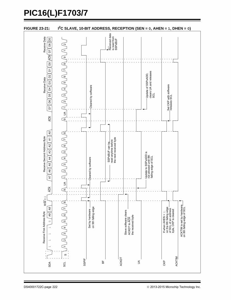
PIC16(L)F1703/7
FIGURE 23-21: I2C SLAVE, 10-BIT ADDRESS, RECEPTION (SEN = 0, AHEN = 1, DHEN = 0)
Rec
eiv
e F
irst
Add
ress
Byt
e
UA
Rec
eiv
e S
eco
nd A
ddre
ss B
yte
UA
Rec
eiv
e D
ata
AC
K
Rec
eive
Dat
a
11
11
0A
9A
8A
7A
6A
5A
4A
3A
2A
1A
0D
7D
6D
5D
4D
3D
2D
1D
0D
7D
6D
5S
DA
SC
L
SS
PIF
BF
AC
KD
T
UA
CK
P
AC
KT
IM
12
34
56
78
9S
AC
KA
CK
12
34
56
78
91
23
45
67
89
12
SS
PxB
UF
is r
ead
fro
m
Rec
eiv
ed d
ata
SS
PxB
UF
can
be
read
any
time
bef
ore
the
ne
xt r
ece
ived
byt
e
Cle
ared
by
softw
are
falli
ng e
dge
of S
CL
not a
llow
ed u
ntil
9th
Upd
ate
to S
SP
xAD
D is
Set
CK
P w
ith s
oftw
are
rele
ases
SC
L
SC
Lcl
ears
UA
and
rel
eas
esU
pda
te o
f SS
PxA
DD
,
Se
t by
hard
wa
reo
n 9
th f
allin
g e
dge
Sla
ve s
oftw
are
cle
ars
AC
KD
T to
AC
Kth
e re
ceiv
ed b
yte
If w
hen
AH
EN
=1
;o
n th
e 8
th f
allin
g e
dge
of S
CL
of a
n a
ddre
ssb
yte,
CK
P is
cle
are
d
AC
KT
IM is
se
t by
hard
wa
reon
8th
falli
ng
edg
e of
SC
L
Cle
are
d b
y so
ftwar
e
R/W
= 0
DS40001722C-page 222 2013-2015 Microchip Technology Inc.
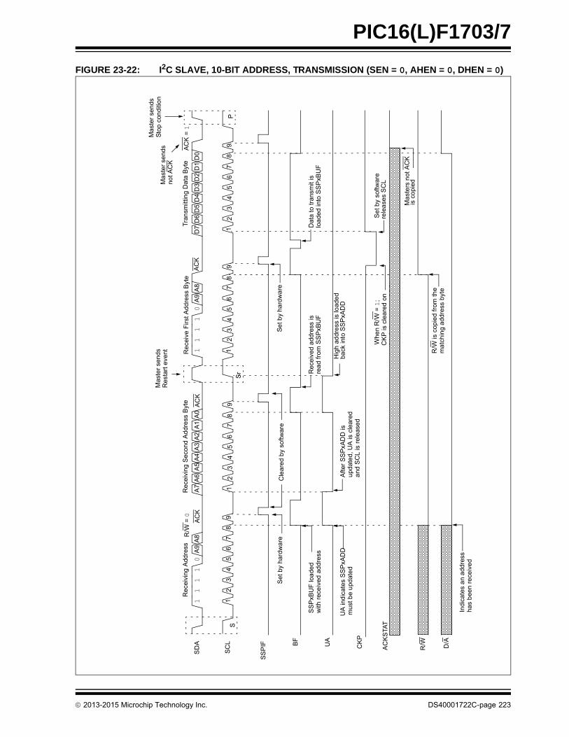
PIC16(L)F1703/7
FIGURE 23-22: I2C SLAVE, 10-BIT ADDRESS, TRANSMISSION (SEN = 0, AHEN = 0, DHEN = 0)
Rec
eivi
ng A
ddre
ss
AC
K
Rec
eiv
ing
Sec
ond
Ad
dre
ss B
yte
Sr
Re
ceiv
e F
irst
Add
ress
Byt
e
AC
K
Tra
nsm
ittin
g D
ata
Byt
e
11
11
0A
9A
8A
7A
6A
5A
4A
3A
2A
1A
01
11
10
A9
A8
D7
D6
D5
D4
D3
D2
D1
D0
SD
A
SC
L
SS
PIF B
F
UA
CK
P
R/W D/A
12
34
56
78
91
23
45
67
89
12
34
56
78
91
23
45
67
89AC
K =
1
P
Ma
ster
sen
ds
Sto
p c
ondi
tion
Ma
ste
r se
nds
not A
CK
Mas
ter
send
s R
esta
rt e
vent
AC
K
R/W
= 0
S
Cle
are
d b
y so
ftwar
e
Aft
er S
SP
xAD
D is
upd
ate
d, U
A is
cle
ared
and
SC
L is
rel
eas
ed
Hig
h a
ddr
ess
is lo
ade
d
Rec
eive
d a
ddre
ss is
Dat
a to
tran
smit
is
Se
t by
softw
are
Indi
cate
s a
n a
ddre
ss
Whe
n R
/W =
1;
R/W
is c
opie
d fr
om th
e
Se
t by
hard
wa
re
UA
ind
icat
es
SS
PxA
DD
SS
PxB
UF
loa
ded
with
rec
eiv
ed a
ddr
ess
mus
t be
upd
ate
d
has
bee
n r
ece
ive
d
loa
ded
into
SS
PxB
UF
rele
ase
s S
CL
Ma
ste
rs n
ot A
CK
is c
opi
ed
ma
tchi
ng
add
ress
byt
e
CK
P is
cle
are
d o
n9t
h fa
lling
ed
ge o
f SC
L
rea
d fr
om S
SP
xBU
F
back
into
SS
PxA
DD
AC
KS
TAT
Set
by
hard
wa
re
2013-2015 Microchip Technology Inc. DS40001722C-page 223
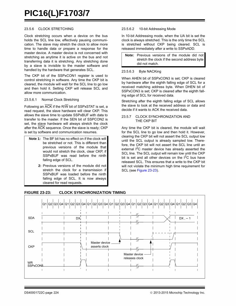
PIC16(L)F1703/7
23.5.6 CLOCK STRETCHING
Clock stretching occurs when a device on the busholds the SCL line low, effectively pausing communi-cation. The slave may stretch the clock to allow moretime to handle data or prepare a response for themaster device. A master device is not concerned withstretching as anytime it is active on the bus and nottransferring data it is stretching. Any stretching doneby a slave is invisible to the master software andhandled by the hardware that generates SCL.
The CKP bit of the SSPxCON1 register is used tocontrol stretching in software. Any time the CKP bit iscleared, the module will wait for the SCL line to go lowand then hold it. Setting CKP will release SCL andallow more communication.
23.5.6.1 Normal Clock Stretching
Following an ACK if the R/W bit of SSPxSTAT is set, aread request, the slave hardware will clear CKP. Thisallows the slave time to update SSPxBUF with data totransfer to the master. If the SEN bit of SSPCON2 isset, the slave hardware will always stretch the clockafter the ACK sequence. Once the slave is ready; CKPis set by software and communication resumes.
23.5.6.2 10-bit Addressing Mode
In 10-bit Addressing mode, when the UA bit is set theclock is always stretched. This is the only time the SCLis stretched without CKP being cleared. SCL isreleased immediately after a write to SSPxADD.
23.5.6.3 Byte NACKing
When AHEN bit of SSPxCON3 is set; CKP is clearedby hardware after the eighth falling edge of SCL for areceived matching address byte. When DHEN bit ofSSPxCON3 is set; CKP is cleared after the eighth fall-ing edge of SCL for received data.
Stretching after the eighth falling edge of SCL allowsthe slave to look at the received address or data anddecide if it wants to ACK the received data.
23.5.7 CLOCK SYNCHRONIZATION AND THE CKP BIT
Any time the CKP bit is cleared, the module will waitfor the SCL line to go low and then hold it. However,clearing the CKP bit will not assert the SCL output lowuntil the SCL output is already sampled low. There-fore, the CKP bit will not assert the SCL line until anexternal I2C master device has already asserted theSCL line. The SCL output will remain low until the CKPbit is set and all other devices on the I2C bus havereleased SCL. This ensures that a write to the CKP bitwill not violate the minimum high time requirement forSCL (see Figure 23-23).
FIGURE 23-23: CLOCK SYNCHRONIZATION TIMING
Note 1: The BF bit has no effect on if the clock willbe stretched or not. This is different thanprevious versions of the module thatwould not stretch the clock, clear CKP, ifSSPxBUF was read before the ninthfalling edge of SCL.
2: Previous versions of the module did notstretch the clock for a transmission ifSSPxBUF was loaded before the ninthfalling edge of SCL. It is now alwayscleared for read requests.
Note: Previous versions of the module did notstretch the clock if the second address bytedid not match.
SDA
SCL
DX ‚ – 1DX
WR
Q1 Q2 Q3 Q4 Q1 Q2 Q3 Q4 Q1 Q2 Q3 Q4 Q1 Q2 Q3 Q4 Q1 Q2 Q3 Q4 Q1 Q2 Q3 Q4 Q1 Q2 Q3 Q4
SSPxCON1
CKP
Master devicereleases clock
Master deviceasserts clock
DS40001722C-page 224 2013-2015 Microchip Technology Inc.
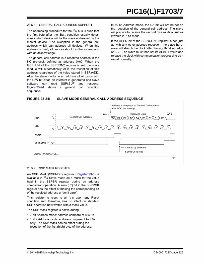
PIC16(L)F1703/7
23.5.8 GENERAL CALL ADDRESS SUPPORT
The addressing procedure for the I2C bus is such thatthe first byte after the Start condition usually deter-mines which device will be the slave addressed by themaster device. The exception is the general calladdress which can address all devices. When thisaddress is used, all devices should, in theory, respondwith an acknowledge.
The general call address is a reserved address in theI2C protocol, defined as address 0x00. When theGCEN bit of the SSPCON2 register is set, the slavemodule will automatically ACK the reception of thisaddress regardless of the value stored in SSPxADD.After the slave clocks in an address of all zeros withthe R/W bit clear, an interrupt is generated and slavesoftware can read SSPxBUF and respond.Figure 23-24 shows a general call receptionsequence.
In 10-bit Address mode, the UA bit will not be set onthe reception of the general call address. The slavewill prepare to receive the second byte as data, just asit would in 7-bit mode.
If the AHEN bit of the SSPxCON3 register is set, justas with any other address reception, the slave hard-ware will stretch the clock after the eighth falling edgeof SCL. The slave must then set its ACKDT value andrelease the clock with communication progressing as itwould normally.
FIGURE 23-24: SLAVE MODE GENERAL CALL ADDRESS SEQUENCE
23.5.9 SSP MASK REGISTER
An SSP Mask (SSPMSK) register (Register 23-5) isavailable in I2C Slave mode as a mask for the valueheld in the SSPSR register during an addresscomparison operation. A zero (‘0’) bit in the SSPMSKregister has the effect of making the corresponding bitof the received address a “don’t care”.
This register is reset to all ‘1’s upon any Resetcondition and, therefore, has no effect on standardSSP operation until written with a mask value.
The SSP Mask register is active during:
• 7-bit Address mode: address compare of A<7:1>.
• 10-bit Address mode: address compare of A<7:0> only. The SSP mask has no effect during the reception of the first (high) byte of the address.
SDA
SCL
S
SSPIF
BF (SSPxSTAT<0>)
Cleared by software
SSPxBUF is read
R/W = 0
ACKGeneral Call Address
Address is compared to General Call Address
Receiving Data ACK
1 2 3 4 5 6 7 8 9 1 2 3 4 5 6 7 8 9
D7 D6 D5 D4 D3 D2 D1 D0
after ACK, set interrupt
GCEN (SSPCON2<7>)
’1’
2013-2015 Microchip Technology Inc. DS40001722C-page 225

PIC16(L)F1703/7
23.6 I2C Master Mode
Master mode is enabled by setting and clearing theappropriate SSPM bits in the SSPxCON1 register andby setting the SSPEN bit. In Master mode, the SDA andSCK pins must be configured as inputs. The MSSPperipheral hardware will override the output driver TRIScontrols when necessary to drive the pins low.
Master mode of operation is supported by interruptgeneration on the detection of the Start and Stopconditions. The Stop (P) and Start (S) bits are clearedfrom a Reset or when the MSSP module is disabled.Control of the I2C bus may be taken when the P bit isset, or the bus is Idle.
In Firmware Controlled Master mode, user codeconducts all I2C bus operations based on Start andStop bit condition detection. Start and Stop conditiondetection is the only active circuitry in this mode. Allother communication is done by the user softwaredirectly manipulating the SDA and SCL lines.
The following events will cause the SSP Interrupt Flagbit, SSPIF, to be set (SSP interrupt, if enabled):
• Start condition detected
• Stop condition detected
• Data transfer byte transmitted/received
• Acknowledge transmitted/received
• Repeated Start generated
23.6.1 I2C MASTER MODE OPERATION
The master device generates all of the serial clockpulses and the Start and Stop conditions. A transfer isended with a Stop condition or with a Repeated Startcondition. Since the Repeated Start condition is alsothe beginning of the next serial transfer, the I2C bus willnot be released.
In Master Transmitter mode, serial data is outputthrough SDA, while SCL outputs the serial clock. Thefirst byte transmitted contains the slave address of thereceiving device (7 bits) and the Read/Write (R/W) bit.In this case, the R/W bit will be logic ‘0’. Serial data istransmitted eight bits at a time. After each byte istransmitted, an Acknowledge bit is received. Start andStop conditions are output to indicate the beginningand the end of a serial transfer.
In Master Receive mode, the first byte transmittedcontains the slave address of the transmitting device(7 bits) and the R/W bit. In this case, the R/W bit will belogic ‘1’. Thus, the first byte transmitted is a 7-bit slaveaddress followed by a ‘1’ to indicate the receive bit.Serial data is received via SDA, while SCL outputs theserial clock. Serial data is received eight bits at a time.After each byte is received, an Acknowledge bit istransmitted. Start and Stop conditions indicate thebeginning and end of transmission.
A Baud Rate Generator is used to set the clockfrequency output on SCL. See Section 23.7 “BaudRate Generator” for more detail.Note 1: The MSSP module, when configured in
I2C Master mode, does not allow queuingof events. For instance, the user is notallowed to initiate a Start condition andimmediately write the SSPxBUF registerto initiate transmission before the Startcondition is complete. In this case, theSSPxBUF will not be written to and theWCOL bit will be set, indicating that awrite to the SSPxBUF did not occur
2: When in Master mode, Start/Stopdetection is masked and an interrupt isgenerated when the SEN/PEN bit iscleared and the generation is complete.
DS40001722C-page 226 2013-2015 Microchip Technology Inc.
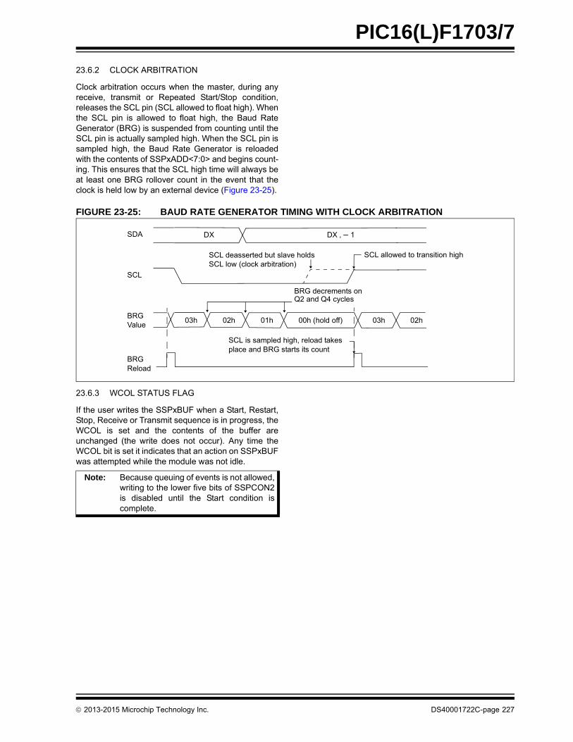
PIC16(L)F1703/7
23.6.2 CLOCK ARBITRATION
Clock arbitration occurs when the master, during anyreceive, transmit or Repeated Start/Stop condition,releases the SCL pin (SCL allowed to float high). Whenthe SCL pin is allowed to float high, the Baud RateGenerator (BRG) is suspended from counting until theSCL pin is actually sampled high. When the SCL pin issampled high, the Baud Rate Generator is reloadedwith the contents of SSPxADD<7:0> and begins count-ing. This ensures that the SCL high time will always beat least one BRG rollover count in the event that theclock is held low by an external device (Figure 23-25).
FIGURE 23-25: BAUD RATE GENERATOR TIMING WITH CLOCK ARBITRATION
23.6.3 WCOL STATUS FLAG
If the user writes the SSPxBUF when a Start, Restart,Stop, Receive or Transmit sequence is in progress, theWCOL is set and the contents of the buffer areunchanged (the write does not occur). Any time theWCOL bit is set it indicates that an action on SSPxBUFwas attempted while the module was not idle.
SDA
SCL
SCL deasserted but slave holds
DX ‚ – 1DX
BRG
SCL is sampled high, reload takesplace and BRG starts its count
03h 02h 01h 00h (hold off) 03h 02h
Reload
BRGValue
SCL low (clock arbitration)SCL allowed to transition high
BRG decrements onQ2 and Q4 cycles
Note: Because queuing of events is not allowed,writing to the lower five bits of SSPCON2is disabled until the Start condition iscomplete.
2013-2015 Microchip Technology Inc. DS40001722C-page 227

PIC16(L)F1703/7
23.6.4 I2C MASTER MODE START CONDITION TIMING
To initiate a Start condition (Figure 23-26), the usersets the Start Enable bit, SEN bit of the SSPCON2register. If the SDA and SCL pins are sampled high,the Baud Rate Generator is reloaded with the contentsof SSPxADD<7:0> and starts its count. If SCL andSDA are both sampled high when the Baud Rate Gen-erator times out (TBRG), the SDA pin is driven low. Theaction of the SDA being driven low while SCL is high isthe Start condition and causes the S bit of theSSPxSTAT1 register to be set. Following this, theBaud Rate Generator is reloaded with the contents ofSSPxADD<7:0> and resumes its count. When theBaud Rate Generator times out (TBRG), the SEN bit ofthe SSPCON2 register will be automatically cleared by
hardware; the Baud Rate Generator is suspended,leaving the SDA line held low and the Start condition iscomplete.
FIGURE 23-26: FIRST START BIT TIMING
Note 1: If at the beginning of the Start condition,the SDA and SCL pins are alreadysampled low, or if during the Start condi-tion, the SCL line is sampled low beforethe SDA line is driven low, a bus collisionoccurs, the Bus Collision Interrupt Flag,BCLIF, is set, the Start condition isaborted and the I2C module is reset intoits Idle state.
2: The Philips I2C specification states that abus collision cannot occur on a Start.
SDA
SCLS
TBRG
1st bit 2nd bit
TBRG
SDA = 1, At completion of Start bit,
SCL = 1
Write to SSPxBUF occurs hereTBRG
hardware clears SEN bit
TBRG
Write to SEN bit occurs here Set S bit (SSPxSTAT<3>)
and sets SSPIF bit
DS40001722C-page 228 2013-2015 Microchip Technology Inc.
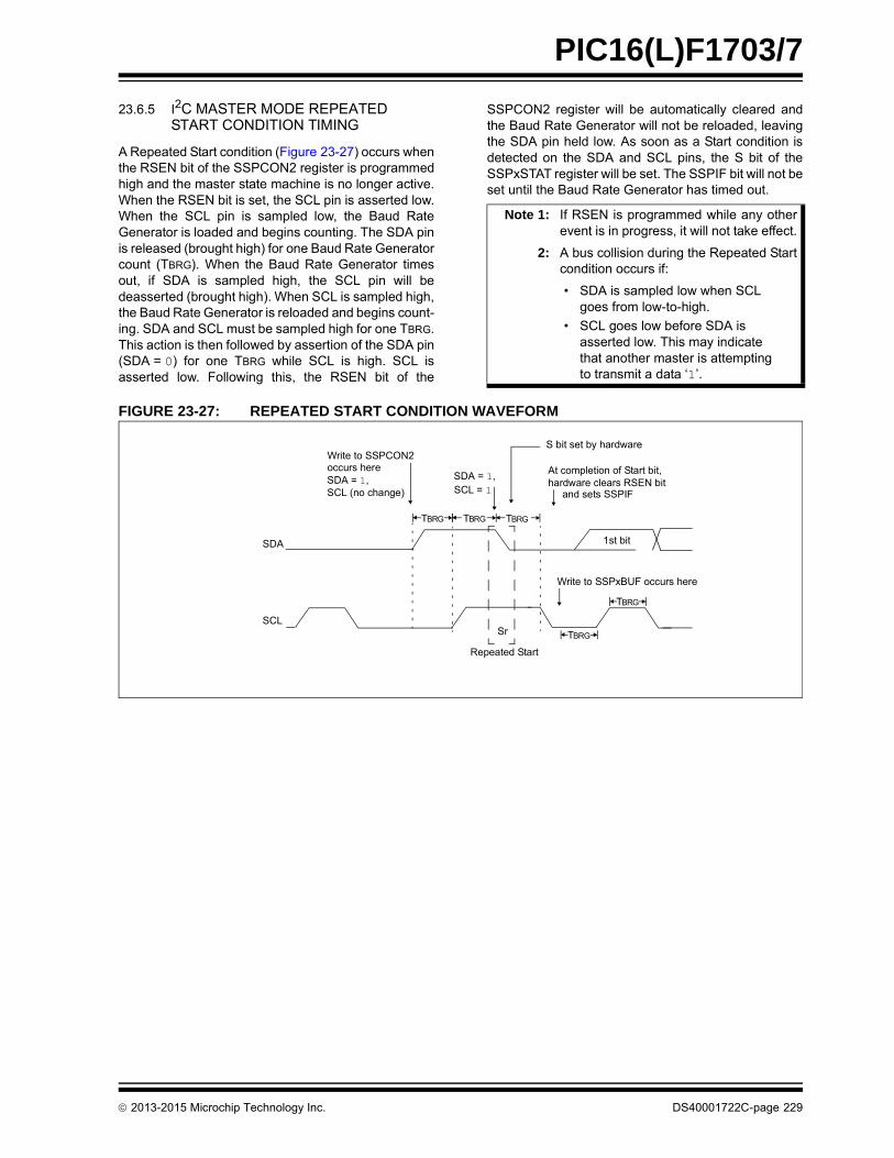
PIC16(L)F1703/7
23.6.5 I2C MASTER MODE REPEATED START CONDITION TIMING
A Repeated Start condition (Figure 23-27) occurs whenthe RSEN bit of the SSPCON2 register is programmedhigh and the master state machine is no longer active.When the RSEN bit is set, the SCL pin is asserted low.When the SCL pin is sampled low, the Baud RateGenerator is loaded and begins counting. The SDA pinis released (brought high) for one Baud Rate Generatorcount (TBRG). When the Baud Rate Generator timesout, if SDA is sampled high, the SCL pin will bedeasserted (brought high). When SCL is sampled high,the Baud Rate Generator is reloaded and begins count-ing. SDA and SCL must be sampled high for one TBRG.This action is then followed by assertion of the SDA pin(SDA = 0) for one TBRG while SCL is high. SCL isasserted low. Following this, the RSEN bit of the
SSPCON2 register will be automatically cleared andthe Baud Rate Generator will not be reloaded, leavingthe SDA pin held low. As soon as a Start condition isdetected on the SDA and SCL pins, the S bit of theSSPxSTAT register will be set. The SSPIF bit will not beset until the Baud Rate Generator has timed out.
FIGURE 23-27: REPEATED START CONDITION WAVEFORM
Note 1: If RSEN is programmed while any otherevent is in progress, it will not take effect.
2: A bus collision during the Repeated Startcondition occurs if:
• SDA is sampled low when SCL goes from low-to-high.
• SCL goes low before SDA is asserted low. This may indicate that another master is attempting to transmit a data ‘1’.
SDA
SCL
Repeated Start
Write to SSPCON2
Write to SSPxBUF occurs here
At completion of Start bit, hardware clears RSEN bit
1st bit
S bit set by hardware
TBRG
TBRG
SDA = 1, SDA = 1,
SCL (no change) SCL = 1
occurs here
TBRG TBRG TBRG
and sets SSPIF
Sr
2013-2015 Microchip Technology Inc. DS40001722C-page 229
PIC16(L)F1703/7
23.6.6 I2C MASTER MODE TRANSMISSION
Transmission of a data byte, a 7-bit address or theother half of a 10-bit address is accomplished by simplywriting a value to the SSPxBUF register. This action willset the Buffer Full flag bit, BF, and allow the Baud RateGenerator to begin counting and start the next trans-mission. Each bit of address/data will be shifted outonto the SDA pin after the falling edge of SCL isasserted. SCL is held low for one Baud Rate Generatorrollover count (TBRG). Data should be valid before SCLis released high. When the SCL pin is released high, itis held that way for TBRG. The data on the SDA pinmust remain stable for that duration and some holdtime after the next falling edge of SCL. After the eighthbit is shifted out (the falling edge of the eighth clock),the BF flag is cleared and the master releases SDA.This allows the slave device being addressed torespond with an ACK bit during the ninth bit time if anaddress match occurred, or if data was received prop-erly. The status of ACK is written into the ACKSTAT biton the rising edge of the ninth clock. If the masterreceives an Acknowledge, the Acknowledge Status bit,ACKSTAT, is cleared. If not, the bit is set. After the ninthclock, the SSPIF bit is set and the master clock (BaudRate Generator) is suspended until the next data byteis loaded into the SSPxBUF, leaving SCL low and SDAunchanged (Figure 23-28).
After the write to the SSPxBUF, each bit of the addresswill be shifted out on the falling edge of SCL until allseven address bits and the R/W bit are completed. Onthe falling edge of the eighth clock, the master willrelease the SDA pin, allowing the slave to respond withan Acknowledge. On the falling edge of the ninth clock,the master will sample the SDA pin to see if the addresswas recognized by a slave. The status of the ACK bit isloaded into the ACKSTAT Status bit of the SSPCON2register. Following the falling edge of the ninth clocktransmission of the address, the SSPIF is set, the BFflag is cleared and the Baud Rate Generator is turnedoff until another write to the SSPxBUF takes place,holding SCL low and allowing SDA to float.
23.6.6.1 BF Status Flag
In Transmit mode, the BF bit of the SSPxSTAT registeris set when the CPU writes to SSPxBUF and is clearedwhen all eight bits are shifted out.
23.6.6.2 WCOL Status Flag
If the user writes the SSPxBUF when a transmit isalready in progress (i.e., SSPSR is still shifting out adata byte), the WCOL bit is set and the contents of thebuffer are unchanged (the write does not occur).
WCOL must be cleared by software before the nexttransmission.
23.6.6.3 ACKSTAT Status Flag
In Transmit mode, the ACKSTAT bit of the SSPCON2register is cleared when the slave has sent an Acknowl-edge (ACK = 0) and is set when the slave does notAcknowledge (ACK = 1). A slave sends an Acknowl-edge when it has recognized its address (including ageneral call), or when the slave has properly receivedits data.
23.6.6.4 Typical transmit sequence:
1. The user generates a Start condition by settingthe SEN bit of the SSPCON2 register.
2. SSPIF is set by hardware on completion of theStart.
3. SSPIF is cleared by software.
4. The MSSP module will wait the required starttime before any other operation takes place.
5. The user loads the SSPxBUF with the slaveaddress to transmit.
6. Address is shifted out the SDA pin until all eightbits are transmitted. Transmission begins assoon as SSPxBUF is written to.
7. The MSSP module shifts in the ACK bit from theslave device and writes its value into theACKSTAT bit of the SSPCON2 register.
8. The MSSP module generates an interrupt at theend of the ninth clock cycle by setting the SSPIFbit.
9. The user loads the SSPxBUF with eight bits ofdata.
10. Data is shifted out the SDA pin until all eight bitsare transmitted.
11. The MSSP module shifts in the ACK bit from theslave device and writes its value into theACKSTAT bit of the SSPCON2 register.
12. Steps 8-11 are repeated for all transmitted databytes.
13. The user generates a Stop or Restart conditionby setting the PEN or RSEN bits of theSSPCON2 register. Interrupt is generated oncethe Stop/Restart condition is complete.
DS40001722C-page 230 2013-2015 Microchip Technology Inc.
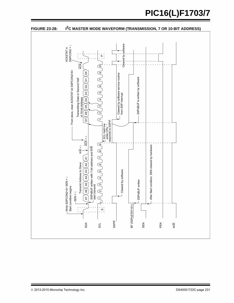
PIC16(L)F1703/7
FIGURE 23-28: I2C MASTER MODE WAVEFORM (TRANSMISSION, 7 OR 10-BIT ADDRESS)
SD
A
SC
L
SS
PIF
BF
(S
SP
xSTA
T<
0>
)
SE
N
A7
A6
A5
A4
A3
A2
A1
AC
K =
0D
7D
6D
5D
4D
3D
2D
1D
0
AC
KT
ran
smitt
ing
Dat
a o
r S
eco
nd H
alf
R/W
= 0
Tra
nsm
it A
ddr
ess
to S
lave
12
34
56
78
91
23
45
67
89
P
Cle
are
d b
y so
ftwar
e se
rvic
e r
out
ine
SS
PxB
UF
is w
ritte
n by
so
ftwa
re
from
SS
P in
terr
upt
Afte
r S
tart
co
nditi
on,
SE
N c
lear
ed b
y h
ardw
are
S
SS
PxB
UF
writ
ten
with
7-b
it a
ddre
ss a
nd
R/W
star
t tra
nsm
it
SC
L h
eld
low
whi
le C
PU
resp
ond
s to
SS
PIF
SE
N =
0
of 1
0-b
it A
ddre
ss
Wri
te S
SP
CO
N2
<0>
SE
N =
1S
tart
con
ditio
n b
egin
sF
rom
sla
ve,
clea
r A
CK
STA
T b
it S
SP
CO
N2<
6>
AC
KS
TAT
in
SS
PC
ON
2 =
1
Cle
ared
by
softw
are
SS
PxB
UF
writ
ten
PE
N
R/W
Cle
are
d b
y so
ftwar
e
2013-2015 Microchip Technology Inc. DS40001722C-page 231
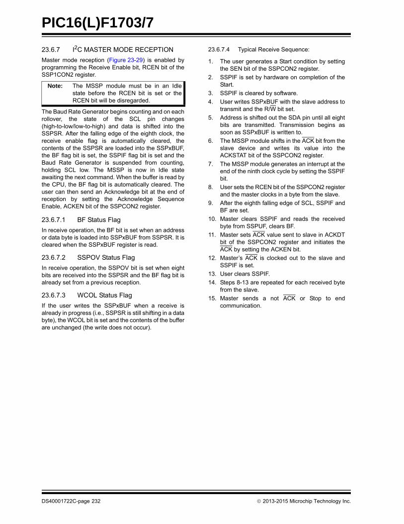
PIC16(L)F1703/7
23.6.7 I2C MASTER MODE RECEPTION
Master mode reception (Figure 23-29) is enabled byprogramming the Receive Enable bit, RCEN bit of theSSP1CON2 register.
The Baud Rate Generator begins counting and on eachrollover, the state of the SCL pin changes(high-to-low/low-to-high) and data is shifted into theSSPSR. After the falling edge of the eighth clock, thereceive enable flag is automatically cleared, thecontents of the SSPSR are loaded into the SSPxBUF,the BF flag bit is set, the SSPIF flag bit is set and theBaud Rate Generator is suspended from counting,holding SCL low. The MSSP is now in Idle stateawaiting the next command. When the buffer is read bythe CPU, the BF flag bit is automatically cleared. Theuser can then send an Acknowledge bit at the end ofreception by setting the Acknowledge SequenceEnable, ACKEN bit of the SSPCON2 register.
23.6.7.1 BF Status Flag
In receive operation, the BF bit is set when an addressor data byte is loaded into SSPxBUF from SSPSR. It iscleared when the SSPxBUF register is read.
23.6.7.2 SSPOV Status Flag
In receive operation, the SSPOV bit is set when eightbits are received into the SSPSR and the BF flag bit isalready set from a previous reception.
23.6.7.3 WCOL Status Flag
If the user writes the SSPxBUF when a receive isalready in progress (i.e., SSPSR is still shifting in a databyte), the WCOL bit is set and the contents of the bufferare unchanged (the write does not occur).
23.6.7.4 Typical Receive Sequence:
1. The user generates a Start condition by settingthe SEN bit of the SSPCON2 register.
2. SSPIF is set by hardware on completion of theStart.
3. SSPIF is cleared by software.
4. User writes SSPxBUF with the slave address totransmit and the R/W bit set.
5. Address is shifted out the SDA pin until all eightbits are transmitted. Transmission begins assoon as SSPxBUF is written to.
6. The MSSP module shifts in the ACK bit from theslave device and writes its value into theACKSTAT bit of the SSPCON2 register.
7. The MSSP module generates an interrupt at theend of the ninth clock cycle by setting the SSPIFbit.
8. User sets the RCEN bit of the SSPCON2 registerand the master clocks in a byte from the slave.
9. After the eighth falling edge of SCL, SSPIF andBF are set.
10. Master clears SSPIF and reads the receivedbyte from SSPUF, clears BF.
11. Master sets ACK value sent to slave in ACKDTbit of the SSPCON2 register and initiates theACK by setting the ACKEN bit.
12. Master’s ACK is clocked out to the slave andSSPIF is set.
13. User clears SSPIF.
14. Steps 8-13 are repeated for each received bytefrom the slave.
15. Master sends a not ACK or Stop to endcommunication.
Note: The MSSP module must be in an Idlestate before the RCEN bit is set or theRCEN bit will be disregarded.
DS40001722C-page 232 2013-2015 Microchip Technology Inc.
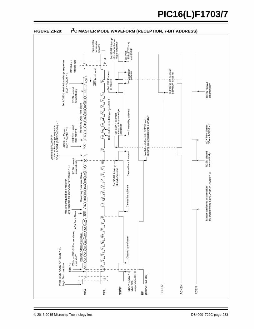
PIC16(L)F1703/7
FIGURE 23-29: I2C MASTER MODE WAVEFORM (RECEPTION, 7-BIT ADDRESS)
P9
87
65
D0
D1
D2
D3
D4
D5
D6
D7
S
A7
A6
A5
A4
A3
A2
A1
SD
A
SC
L1
23
45
67
89
12
34
56
78
91
23
4
Bu
s m
aste
rte
rmin
ate
str
ansf
er
AC
K
Re
ceiv
ing
Dat
a fr
om
Sla
veR
ece
ivin
g D
ata
from
Sla
ve
D0
D1
D2
D3
D4
D5
D6
D7
AC
KR
/W
Tra
nsm
it A
dd
ress
to
Sla
ve
SS
PIF
BF
AC
K is
no
t se
nt
Wri
te to
SS
PC
ON
2<
0>
(SE
N =
1),
Writ
e to
SS
PxB
UF
occ
urs
her
e,
AC
K fr
om
Sla
veMa
ste
r co
nfig
ure
d a
s a
re
ceiv
er
by p
rog
ram
min
g S
SP
CO
N2
<3
> (
RC
EN
= 1
)P
EN
bit
= 1
wri
tten
he
re
Da
ta s
hifte
d in
on
falli
ng
edg
e o
f CL
K
Cle
are
d b
y so
ftwar
e
sta
rt X
MIT
SE
N =
0
SS
PO
V
SD
A =
0,
SC
L =
1w
hile
CP
U
(SS
PxS
TAT
<0>
)
AC
K
Cle
are
d b
y so
ftwa
reC
lea
red
by
softw
are
Set
SS
PIF
inte
rru
pt
at
end
of
rece
ive
Se
t P
bit
(SS
PxS
TAT
<4
>)
and
SS
PIF
Cle
are
d in
softw
are
AC
K f
rom
Mas
ter
Se
t S
SP
IF a
t e
nd
Se
t S
SP
IF in
terr
upt
at e
nd
of
Ack
no
wle
dg
ese
qu
en
ce
Se
t S
SP
IF in
terr
up
ta
t en
d o
f Ack
now
-le
dg
e se
qu
ence
of r
ece
ive
Se
t A
CK
EN
, st
art
Ack
no
wle
dge
se
que
nce
SS
PO
V is
se
t b
eca
use
SS
PxB
UF
is s
till f
ull
SD
A =
AC
KD
T =
1
RC
EN
cle
are
dau
tom
atic
ally
RC
EN
= 1
, st
art
next
re
ceiv
e
Wri
te t
o S
SP
CO
N2
<4
>to
sta
rt A
ckno
wle
dge
sequ
ence
SD
A =
AC
KD
T (
SS
PC
ON
2<
5>
) =
0
RC
EN
cle
are
dau
tom
atic
ally
resp
on
ds
to S
SP
IF
AC
KE
Nbeg
in S
tart
co
nd
itio
n
Cle
are
d b
y so
ftwar
e
SD
A =
AC
KD
T =
0
Last
bit
is s
hifte
d in
to S
SP
SR
and
cont
en
ts a
re u
nlo
ade
d in
to S
SP
xBU
F
RC
EN
Ma
ster
co
nfig
ure
d a
s a
re
ceiv
er
by
pro
gra
mm
ing
SS
PC
ON
2<
3>
(R
CE
N =
1)
RC
EN
cle
are
dau
tom
atic
ally
AC
K f
rom
Ma
ste
rS
DA
= A
CK
DT
= 0
R
CE
N c
lea
red
au
tom
atic
ally
2013-2015 Microchip Technology Inc. DS40001722C-page 233
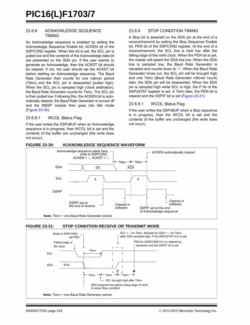
PIC16(L)F1703/7
23.6.8 ACKNOWLEDGE SEQUENCE TIMING
An Acknowledge sequence is enabled by setting theAcknowledge Sequence Enable bit, ACKEN bit of theSSPCON2 register. When this bit is set, the SCL pin ispulled low and the contents of the Acknowledge data bitare presented on the SDA pin. If the user wishes togenerate an Acknowledge, then the ACKDT bit shouldbe cleared. If not, the user should set the ACKDT bitbefore starting an Acknowledge sequence. The BaudRate Generator then counts for one rollover period(TBRG) and the SCL pin is deasserted (pulled high).When the SCL pin is sampled high (clock arbitration),the Baud Rate Generator counts for TBRG. The SCL pinis then pulled low. Following this, the ACKEN bit is auto-matically cleared, the Baud Rate Generator is turned offand the MSSP module then goes into Idle mode(Figure 23-30).
23.6.8.1 WCOL Status Flag
If the user writes the SSPxBUF when an Acknowledgesequence is in progress, then WCOL bit is set and thecontents of the buffer are unchanged (the write doesnot occur).
23.6.9 STOP CONDITION TIMING
A Stop bit is asserted on the SDA pin at the end of areceive/transmit by setting the Stop Sequence Enablebit, PEN bit of the SSPCON2 register. At the end of areceive/transmit, the SCL line is held low after thefalling edge of the ninth clock. When the PEN bit is set,the master will assert the SDA line low. When the SDAline is sampled low, the Baud Rate Generator isreloaded and counts down to ‘0’. When the Baud RateGenerator times out, the SCL pin will be brought highand one TBRG (Baud Rate Generator rollover count)later, the SDA pin will be deasserted. When the SDApin is sampled high while SCL is high, the P bit of theSSPxSTAT register is set. A TBRG later, the PEN bit iscleared and the SSPIF bit is set (Figure 23-31).
23.6.9.1 WCOL Status Flag
If the user writes the SSPxBUF when a Stop sequenceis in progress, then the WCOL bit is set and thecontents of the buffer are unchanged (the write doesnot occur).
FIGURE 23-30: ACKNOWLEDGE SEQUENCE WAVEFORM
FIGURE 23-31: STOP CONDITION RECEIVE OR TRANSMIT MODE
Note: TBRG = one Baud Rate Generator period.
SDA
SCL
SSPIF set at
Acknowledge sequence starts here,write to SSPCON2
ACKEN automatically cleared
Cleared in
TBRG TBRG
the end of receive
8
ACKEN = 1, ACKDT = 0
D0
9
SSPIF
software SSPIF set at the endof Acknowledge sequence
Cleared insoftware
ACK
SCL
SDA
SDA asserted low before rising edge of clock
Write to SSPCON2,set PEN
Falling edge of
SCL = 1 for TBRG, followed by SDA = 1 for TBRG
9th clock
SCL brought high after TBRG
Note: TBRG = one Baud Rate Generator period.
TBRG TBRG
after SDA sampled high. P bit (SSPxSTAT<4>) is set.
TBRG
to setup Stop condition
ACK
P
TBRG
PEN bit (SSPCON2<2>) is cleared by hardware and the SSPIF bit is set
DS40001722C-page 234 2013-2015 Microchip Technology Inc.
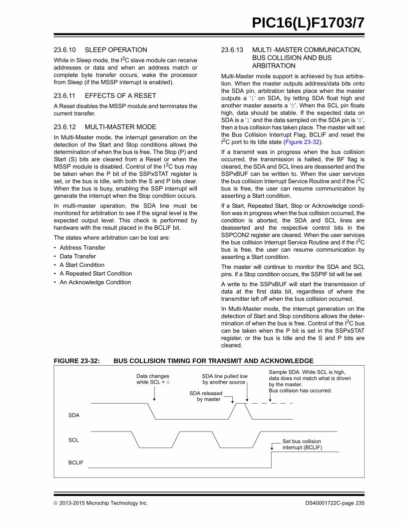
PIC16(L)F1703/7
23.6.10 SLEEP OPERATION
While in Sleep mode, the I2C slave module can receiveaddresses or data and when an address match orcomplete byte transfer occurs, wake the processorfrom Sleep (if the MSSP interrupt is enabled).
23.6.11 EFFECTS OF A RESET
A Reset disables the MSSP module and terminates thecurrent transfer.
23.6.12 MULTI-MASTER MODE
In Multi-Master mode, the interrupt generation on thedetection of the Start and Stop conditions allows thedetermination of when the bus is free. The Stop (P) andStart (S) bits are cleared from a Reset or when theMSSP module is disabled. Control of the I2C bus maybe taken when the P bit of the SSPxSTAT register isset, or the bus is Idle, with both the S and P bits clear.When the bus is busy, enabling the SSP interrupt willgenerate the interrupt when the Stop condition occurs.
In multi-master operation, the SDA line must bemonitored for arbitration to see if the signal level is theexpected output level. This check is performed byhardware with the result placed in the BCLIF bit.
The states where arbitration can be lost are:
• Address Transfer
• Data Transfer
• A Start Condition
• A Repeated Start Condition
• An Acknowledge Condition
23.6.13 MULTI -MASTER COMMUNICATION, BUS COLLISION AND BUS ARBITRATION
Multi-Master mode support is achieved by bus arbitra-tion. When the master outputs address/data bits ontothe SDA pin, arbitration takes place when the masteroutputs a ‘1’ on SDA, by letting SDA float high andanother master asserts a ‘0’. When the SCL pin floatshigh, data should be stable. If the expected data onSDA is a ‘1’ and the data sampled on the SDA pin is ‘0’,then a bus collision has taken place. The master will setthe Bus Collision Interrupt Flag, BCLIF and reset theI2C port to its Idle state (Figure 23-32).
If a transmit was in progress when the bus collisionoccurred, the transmission is halted, the BF flag iscleared, the SDA and SCL lines are deasserted and theSSPxBUF can be written to. When the user servicesthe bus collision Interrupt Service Routine and if the I2Cbus is free, the user can resume communication byasserting a Start condition.
If a Start, Repeated Start, Stop or Acknowledge condi-tion was in progress when the bus collision occurred, thecondition is aborted, the SDA and SCL lines aredeasserted and the respective control bits in theSSPCON2 register are cleared. When the user servicesthe bus collision Interrupt Service Routine and if the I2Cbus is free, the user can resume communication byasserting a Start condition.
The master will continue to monitor the SDA and SCLpins. If a Stop condition occurs, the SSPIF bit will be set.
A write to the SSPxBUF will start the transmission ofdata at the first data bit, regardless of where thetransmitter left off when the bus collision occurred.
In Multi-Master mode, the interrupt generation on thedetection of Start and Stop conditions allows the deter-mination of when the bus is free. Control of the I2C buscan be taken when the P bit is set in the SSPxSTATregister, or the bus is Idle and the S and P bits arecleared.
FIGURE 23-32: BUS COLLISION TIMING FOR TRANSMIT AND ACKNOWLEDGE
SDA
SCL
BCLIF
SDA released
SDA line pulled lowby another source
Sample SDA. While SCL is high,data does not match what is driven
Bus collision has occurred.
Set bus collisioninterrupt (BCLIF)
by the master.
by master
Data changeswhile SCL = 0
2013-2015 Microchip Technology Inc. DS40001722C-page 235

PIC16(L)F1703/7
23.6.13.1 Bus Collision During a Start Condition
During a Start condition, a bus collision occurs if:
a) SDA or SCL are sampled low at the beginning ofthe Start condition (Figure 23-33).
b) SCL is sampled low before SDA is asserted low(Figure 23-34).
During a Start condition, both the SDA and the SCLpins are monitored.
If the SDA pin is already low, or the SCL pin is alreadylow, then all of the following occur:
• the Start condition is aborted,
• the BCLIF flag is set and
• the MSSP module is reset to its Idle state (Figure 23-33).
The Start condition begins with the SDA and SCL pinsdeasserted. When the SDA pin is sampled high, theBaud Rate Generator is loaded and counts down. If theSCL pin is sampled low while SDA is high, a buscollision occurs because it is assumed that anothermaster is attempting to drive a data ‘1’ during the Startcondition.
If the SDA pin is sampled low during this count, theBRG is reset and the SDA line is asserted early(Figure 23-35). If, however, a ‘1’ is sampled on the SDApin, the SDA pin is asserted low at the end of the BRGcount. The Baud Rate Generator is then reloaded andcounts down to zero; if the SCL pin is sampled as ‘0’during this time, a bus collision does not occur. At theend of the BRG count, the SCL pin is asserted low.
FIGURE 23-33: BUS COLLISION DURING START CONDITION (SDA ONLY)
Note: The reason that bus collision is not afactor during a Start condition is that notwo bus masters can assert a Start condi-tion at the exact same time. Therefore,one master will always assert SDA beforethe other. This condition does not cause abus collision because the two mastersmust be allowed to arbitrate the firstaddress following the Start condition. If theaddress is the same, arbitration must beallowed to continue into the data portion,Repeated Start or Stop conditions.
SDA
SCL
SEN
SDA sampled low before
SDA goes low before the SEN bit is set.
S bit and SSPIF set because
SSP module reset into Idle state.SEN cleared automatically because of bus collision.
S bit and SSPIF set because
Set SEN, enable Startcondition if SDA = 1, SCL = 1
SDA = 0, SCL = 1.
BCLIF
S
SSPIF
SDA = 0, SCL = 1.
SSPIF and BCLIF arecleared by software
SSPIF and BCLIF arecleared by software
Set BCLIF,
Start condition. Set BCLIF.
DS40001722C-page 236 2013-2015 Microchip Technology Inc.
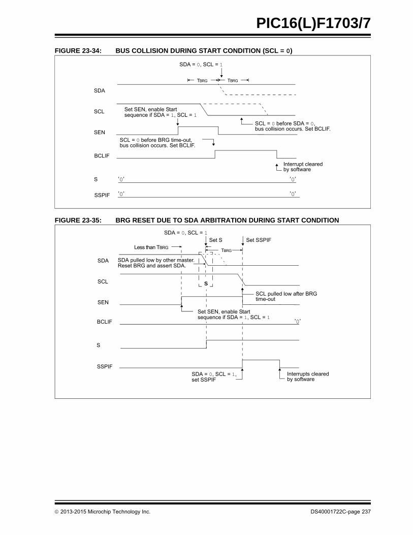
PIC16(L)F1703/7
FIGURE 23-34: BUS COLLISION DURING START CONDITION (SCL = 0)
FIGURE 23-35: BRG RESET DUE TO SDA ARBITRATION DURING START CONDITION
SDA
SCL
SENbus collision occurs. Set BCLIF.SCL = 0 before SDA = 0,
Set SEN, enable Startsequence if SDA = 1, SCL = 1
TBRG TBRG
SDA = 0, SCL = 1
BCLIF
S
SSPIF
Interrupt clearedby software
bus collision occurs. Set BCLIF.SCL = 0 before BRG time-out,
’0’ ’0’
’0’’0’
SDA
SCL
SEN
Set SLess than TBRG
TBRG
SDA = 0, SCL = 1
BCLIF
S
SSPIF
S
Interrupts clearedby softwareset SSPIF
SDA = 0, SCL = 1,
SCL pulled low after BRGtime-out
Set SSPIF
’0’
SDA pulled low by other master.Reset BRG and assert SDA.
Set SEN, enable Startsequence if SDA = 1, SCL = 1
2013-2015 Microchip Technology Inc. DS40001722C-page 237
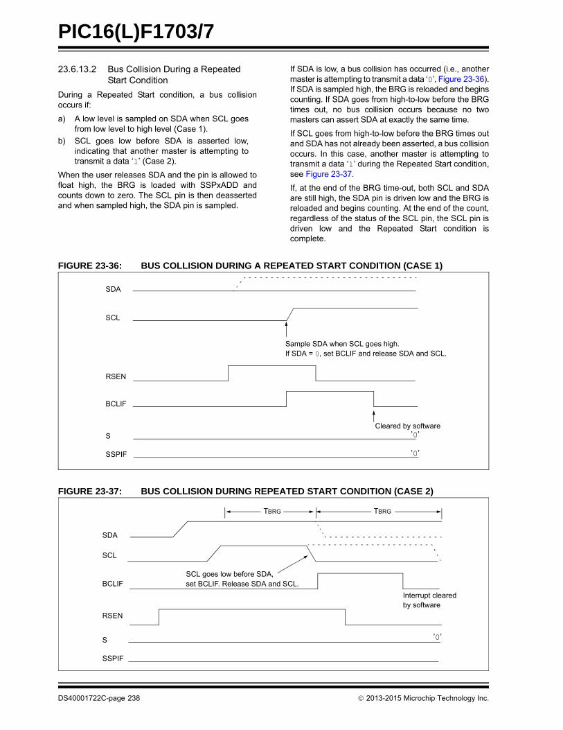
PIC16(L)F1703/7
23.6.13.2 Bus Collision During a Repeated Start Condition
During a Repeated Start condition, a bus collisionoccurs if:
a) A low level is sampled on SDA when SCL goesfrom low level to high level (Case 1).
b) SCL goes low before SDA is asserted low,indicating that another master is attempting totransmit a data ‘1’ (Case 2).
When the user releases SDA and the pin is allowed tofloat high, the BRG is loaded with SSPxADD andcounts down to zero. The SCL pin is then deassertedand when sampled high, the SDA pin is sampled.
If SDA is low, a bus collision has occurred (i.e., anothermaster is attempting to transmit a data ‘0’, Figure 23-36).If SDA is sampled high, the BRG is reloaded and beginscounting. If SDA goes from high-to-low before the BRGtimes out, no bus collision occurs because no twomasters can assert SDA at exactly the same time.
If SCL goes from high-to-low before the BRG times outand SDA has not already been asserted, a bus collisionoccurs. In this case, another master is attempting totransmit a data ‘1’ during the Repeated Start condition,see Figure 23-37.
If, at the end of the BRG time-out, both SCL and SDAare still high, the SDA pin is driven low and the BRG isreloaded and begins counting. At the end of the count,regardless of the status of the SCL pin, the SCL pin isdriven low and the Repeated Start condition iscomplete.
FIGURE 23-36: BUS COLLISION DURING A REPEATED START CONDITION (CASE 1)
FIGURE 23-37: BUS COLLISION DURING REPEATED START CONDITION (CASE 2)
SDA
SCL
RSEN
BCLIF
S
SSPIF
Sample SDA when SCL goes high.If SDA = 0, set BCLIF and release SDA and SCL.
Cleared by software
’0’
’0’
SDA
SCL
BCLIF
RSEN
S
SSPIF
Interrupt clearedby software
SCL goes low before SDA,set BCLIF. Release SDA and SCL.
TBRG TBRG
’0’
DS40001722C-page 238 2013-2015 Microchip Technology Inc.
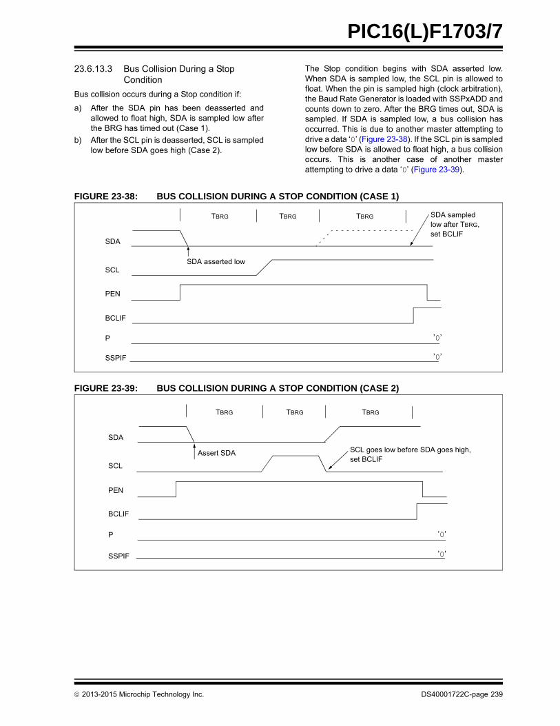
PIC16(L)F1703/7
23.6.13.3 Bus Collision During a Stop Condition
Bus collision occurs during a Stop condition if:
a) After the SDA pin has been deasserted andallowed to float high, SDA is sampled low afterthe BRG has timed out (Case 1).
b) After the SCL pin is deasserted, SCL is sampledlow before SDA goes high (Case 2).
The Stop condition begins with SDA asserted low.When SDA is sampled low, the SCL pin is allowed tofloat. When the pin is sampled high (clock arbitration),the Baud Rate Generator is loaded with SSPxADD andcounts down to zero. After the BRG times out, SDA issampled. If SDA is sampled low, a bus collision hasoccurred. This is due to another master attempting todrive a data ‘0’ (Figure 23-38). If the SCL pin is sampledlow before SDA is allowed to float high, a bus collisionoccurs. This is another case of another masterattempting to drive a data ‘0’ (Figure 23-39).
FIGURE 23-38: BUS COLLISION DURING A STOP CONDITION (CASE 1)
FIGURE 23-39: BUS COLLISION DURING A STOP CONDITION (CASE 2)
SDA
SCL
BCLIF
PEN
P
SSPIF
TBRG TBRG TBRG
SDA asserted low
SDA sampledlow after TBRG,set BCLIF
’0’
’0’
SDA
SCL
BCLIF
PEN
P
SSPIF
TBRG TBRG TBRG
Assert SDA SCL goes low before SDA goes high,set BCLIF
’0’
’0’
2013-2015 Microchip Technology Inc. DS40001722C-page 239
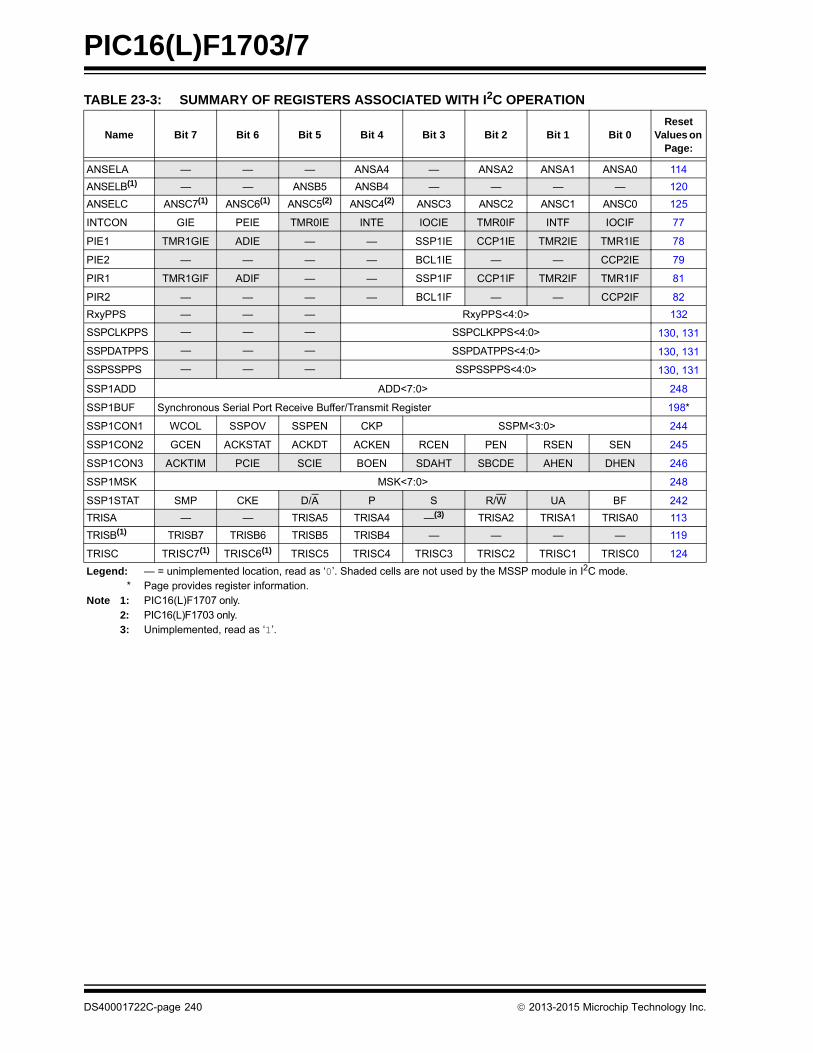
PIC16(L)F1703/7
TABLE 23-3: SUMMARY OF REGISTERS ASSOCIATED WITH I2C OPERATION
Name Bit 7 Bit 6 Bit 5 Bit 4 Bit 3 Bit 2 Bit 1 Bit 0Reset
Values on Page:
ANSELA — — — ANSA4 — ANSA2 ANSA1 ANSA0 114
ANSELB(1) — — ANSB5 ANSB4 — — — — 120
ANSELC ANSC7(1) ANSC6(1) ANSC5(2) ANSC4(2) ANSC3 ANSC2 ANSC1 ANSC0 125
INTCON GIE PEIE TMR0IE INTE IOCIE TMR0IF INTF IOCIF 77
PIE1 TMR1GIE ADIE — — SSP1IE CCP1IE TMR2IE TMR1IE 78
PIE2 — — — — BCL1IE — — CCP2IE 79
PIR1 TMR1GIF ADIF — — SSP1IF CCP1IF TMR2IF TMR1IF 81
PIR2 — — — — BCL1IF — — CCP2IF 82
RxyPPS — — — RxyPPS<4:0> 132
SSPCLKPPS — — — SSPCLKPPS<4:0> 130, 131
SSPDATPPS — — — SSPDATPPS<4:0> 130, 131
SSPSSPPS — — — SSPSSPPS<4:0> 130, 131
SSP1ADD ADD<7:0> 248
SSP1BUF Synchronous Serial Port Receive Buffer/Transmit Register 198*
SSP1CON1 WCOL SSPOV SSPEN CKP SSPM<3:0> 244
SSP1CON2 GCEN ACKSTAT ACKDT ACKEN RCEN PEN RSEN SEN 245
SSP1CON3 ACKTIM PCIE SCIE BOEN SDAHT SBCDE AHEN DHEN 246
SSP1MSK MSK<7:0> 248
SSP1STAT SMP CKE D/A P S R/W UA BF 242
TRISA — — TRISA5 TRISA4 —(3) TRISA2 TRISA1 TRISA0 113
TRISB(1) TRISB7 TRISB6 TRISB5 TRISB4 — — — — 119
TRISC TRISC7(1) TRISC6(1) TRISC5 TRISC4 TRISC3 TRISC2 TRISC1 TRISC0 124
Legend: — = unimplemented location, read as ‘0’. Shaded cells are not used by the MSSP module in I2C mode.* Page provides register information.
Note 1: PIC16(L)F1707 only.2: PIC16(L)F1703 only.3: Unimplemented, read as ‘1’.
DS40001722C-page 240 2013-2015 Microchip Technology Inc.
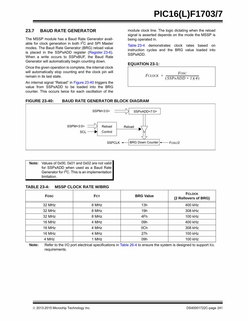
PIC16(L)F1703/7
23.7 BAUD RATE GENERATOR
The MSSP module has a Baud Rate Generator avail-able for clock generation in both I2C and SPI Mastermodes. The Baud Rate Generator (BRG) reload valueis placed in the SSPxADD register (Register 23-6).When a write occurs to SSPxBUF, the Baud RateGenerator will automatically begin counting down.
Once the given operation is complete, the internal clockwill automatically stop counting and the clock pin willremain in its last state.
An internal signal “Reload” in Figure 23-40 triggers thevalue from SSPxADD to be loaded into the BRGcounter. This occurs twice for each oscillation of the
module clock line. The logic dictating when the reloadsignal is asserted depends on the mode the MSSP isbeing operated in.
Table 23-4 demonstrates clock rates based oninstruction cycles and the BRG value loaded intoSSPxADD.
EQUATION 23-1:
FIGURE 23-40: BAUD RATE GENERATOR BLOCK DIAGRAM
TABLE 23-4: MSSP CLOCK RATE W/BRG
FCLOCKFOSC
SSPxADD 1+ 4 -------------------------------------------------=
Note: Values of 0x00, 0x01 and 0x02 are not validfor SSPxADD when used as a Baud RateGenerator for I2C. This is an implementationlimitation.
FOSC FCY BRG ValueFCLOCK
(2 Rollovers of BRG)
32 MHz 8 MHz 13h 400 kHz
32 MHz 8 MHz 19h 308 kHz
32 MHz 8 MHz 4Fh 100 kHz
16 MHz 4 MHz 09h 400 kHz
16 MHz 4 MHz 0Ch 308 kHz
16 MHz 4 MHz 27h 100 kHz
4 MHz 1 MHz 09h 100 kHz
Note: Refer to the I/O port electrical specifications in Table 26-4 to ensure the system is designed to support IOL
requirements.
SSPM<3:0>
BRG Down CounterSSPCLK FOSC/2
SSPxADD<7:0>
SSPM<3:0>
SCL
Reload
Control
Reload
2013-2015 Microchip Technology Inc. DS40001722C-page 241

PIC16(L)F1703/7
23.8 Register Definitions: MSSP Control REGISTER 23-1: SSP1STAT: SSP STATUS REGISTER
R/W-0/0 R/W-0/0 R-0/0 R-0/0 R-0/0 R-0/0 R-0/0 R-0/0
SMP CKE D/A P S R/W UA BF
bit 7 bit 0
Legend:
R = Readable bit W = Writable bit U = Unimplemented bit, read as ‘0’
u = Bit is unchanged x = Bit is unknown -n/n = Value at POR and BOR/Value at all other Resets
‘1’ = Bit is set ‘0’ = Bit is cleared
bit 7 SMP: SPI Data Input Sample bit
SPI Master mode:1 = Input data sampled at end of data output time0 = Input data sampled at middle of data output time
SPI Slave mode:SMP must be cleared when SPI is used in Slave modeIn I2 C Master or Slave mode: 1 = Slew rate control disabled for Standard Speed mode (100 kHz and 1 MHz)0 = Slew rate control enabled for High-Speed mode (400 kHz)
bit 6 CKE: SPI Clock Edge Select bit (SPI mode only)
In SPI Master or Slave mode:1 = Transmit occurs on transition from active to Idle clock state0 = Transmit occurs on transition from Idle to active clock state
In I2 C™ mode only: 1 = Enable input logic so that thresholds are compliant with SMBus specification0 = Disable SMBus specific inputs
bit 5 D/A: Data/Address bit (I2C mode only) 1 = Indicates that the last byte received or transmitted was data0 = Indicates that the last byte received or transmitted was address
bit 4 P: Stop bit
(I2C mode only. This bit is cleared when the MSSP module is disabled, SSPEN is cleared.)1 = Indicates that a Stop bit has been detected last (this bit is ‘0’ on Reset)0 = Stop bit was not detected last
bit 3 S: Start bit
(I2C mode only. This bit is cleared when the MSSP module is disabled, SSPEN is cleared.)1 = Indicates that a Start bit has been detected last (this bit is ‘0’ on Reset)0 = Start bit was not detected last
bit 2 R/W: Read/Write bit information (I2C mode only)This bit holds the R/W bit information following the last address match. This bit is only valid from the address matchto the next Start bit, Stop bit, or not ACK bit.In I2 C Slave mode:1 = Read0 = Write
In I2 C Master mode:1 = Transmit is in progress0 = Transmit is not in progress
OR-ing this bit with SEN, RSEN, PEN, RCEN or ACKEN will indicate if the MSSP is in Idle mode.
bit 1 UA: Update Address bit (10-bit I2C mode only)1 = Indicates that the user needs to update the address in the SSPxADD register0 = Address does not need to be updated
DS40001722C-page 242 2013-2015 Microchip Technology Inc.
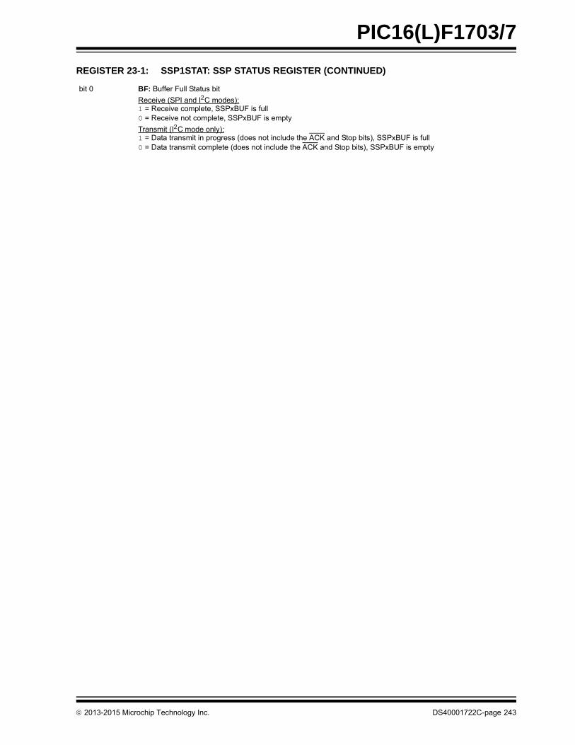
PIC16(L)F1703/7
bit 0 BF: Buffer Full Status bit
Receive (SPI and I2 C modes):1 = Receive complete, SSPxBUF is full0 = Receive not complete, SSPxBUF is empty
Transmit (I2 C mode only):1 = Data transmit in progress (does not include the ACK and Stop bits), SSPxBUF is full0 = Data transmit complete (does not include the ACK and Stop bits), SSPxBUF is empty
REGISTER 23-1: SSP1STAT: SSP STATUS REGISTER (CONTINUED)
2013-2015 Microchip Technology Inc. DS40001722C-page 243

PIC16(L)F1703/7
REGISTER 23-2: SSP1CON1: SSP CONTROL REGISTER 1
R/C/HS-0/0 R/C/HS-0/0 R/W-0/0 R/W-0/0 R/W-0/0 R/W-0/0 R/W-0/0 R/W-0/0
WCOL SSPOV(1) SSPEN CKP SSPM<3:0>
bit 7 bit 0
Legend:
R = Readable bit W = Writable bit U = Unimplemented bit, read as ‘0’
u = Bit is unchanged x = Bit is unknown -n/n = Value at POR and BOR/Value at all other Resets
‘1’ = Bit is set ‘0’ = Bit is cleared HS = Bit is set by hardware C = User cleared
bit 7 WCOL: Write Collision Detect bitMaster mode:1 = A write to the SSPxBUF register was attempted while the I2C conditions were not valid for a transmission to be started0 = No collisionSlave mode:1 = The SSPxBUF register is written while it is still transmitting the previous word (must be cleared in software)0 = No collision
bit 6 SSPOV: Receive Overflow Indicator bit(1)
In SPI mode:1 = A new byte is received while the SSPxBUF register is still holding the previous data. In case of overflow, the data in SSPSR is lost.
Overflow can only occur in Slave mode. In Slave mode, the user must read the SSPxBUF, even if only transmitting data, to avoid setting overflow. In Master mode, the overflow bit is not set since each new reception (and transmission) is initiated by writing to the SSPxBUF register (must be cleared in software).
0 = No overflowIn I2 C mode:1 = A byte is received while the SSPxBUF register is still holding the previous byte. SSPOV is a “don’t care” in Transmit mode
(must be cleared in software). 0 = No overflow
bit 5 SSPEN: Synchronous Serial Port Enable bitIn both modes, when enabled, these pins must be properly configured as input or outputIn SPI mode:1 = Enables serial port and configures SCK, SDO, SDI and SS as the source of the serial port pins(2)
0 = Disables serial port and configures these pins as I/O port pinsIn I2 C mode:1 = Enables the serial port and configures the SDA and SCL pins as the source of the serial port pins(3)
0 = Disables serial port and configures these pins as I/O port pins
bit 4 CKP: Clock Polarity Select bit In SPI mode:1 = Idle state for clock is a high level 0 = Idle state for clock is a low levelIn I2 C Slave mode:SCL release control1 = Enable clock 0 = Holds clock low (clock stretch). (Used to ensure data setup time.)In I2 C Master mode:Unused in this mode
bit 3-0 SSPM<3:0>: Synchronous Serial Port Mode Select bits1111 = I2C Slave mode, 10-bit address with Start and Stop bit interrupts enabled 1110 = I2C Slave mode, 7-bit address with Start and Stop bit interrupts enabled 1101 = Reserved 1100 = Reserved 1011 = I2C firmware controlled Master mode (slave idle) 1010 = SPI Master mode, clock = FOSC/(4 * (SSPxADD+1))(5)
1001 = Reserved1000 = I2C Master mode, clock = FOSC / (4 * (SSPxADD+1))(4)
0111 = I2C Slave mode, 10-bit address 0110 = I2C Slave mode, 7-bit address 0101 = SPI Slave mode, clock = SCK pin, SS pin control disabled, SS can be used as I/O pin0100 = SPI Slave mode, clock = SCK pin, SS pin control enabled 0011 = SPI Master mode, clock = T2_match/2 0010 = SPI Master mode, clock = FOSC/64 0001 = SPI Master mode, clock = FOSC/16 0000 = SPI Master mode, clock = FOSC/4
Note 1: In Master mode, the overflow bit is not set since each new reception (and transmission) is initiated by writing to the SSPxBUF register.2: When enabled, these pins must be properly configured as input or output. Use SSPSSPPS, SSPCLKPPS, SSPDATPPS, and RxyPPS
to select the pins.3: When enabled, the SDA and SCL pins must be configured as inputs. Use SSPCLKPPS, SSPDATPPS, and RxyPPS to select the pins.4: SSPxADD values of 0, 1 or 2 are not supported for I2C mode.5: SSPxADD value of ‘0’ is not supported. Use SSPM = 0000 instead.
DS40001722C-page 244 2013-2015 Microchip Technology Inc.
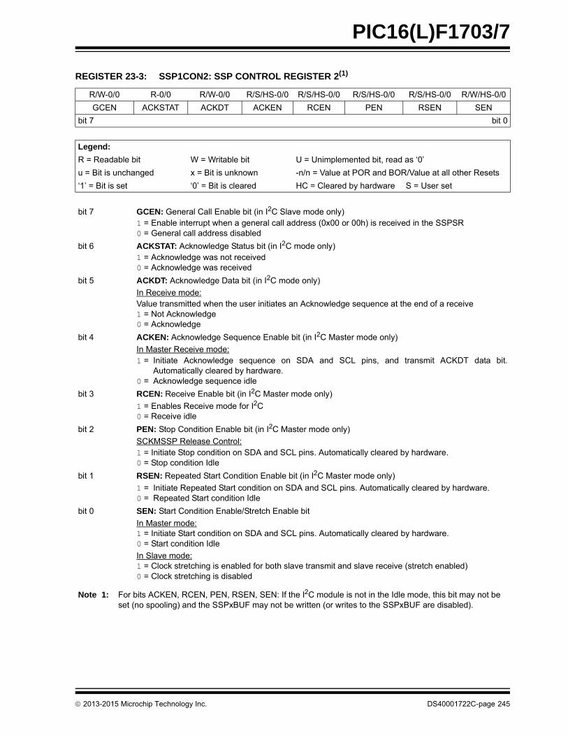
PIC16(L)F1703/7
REGISTER 23-3: SSP1CON2: SSP CONTROL REGISTER 2(1)
R/W-0/0 R-0/0 R/W-0/0 R/S/HS-0/0 R/S/HS-0/0 R/S/HS-0/0 R/S/HS-0/0 R/W/HS-0/0
GCEN ACKSTAT ACKDT ACKEN RCEN PEN RSEN SEN
bit 7 bit 0
Legend:
R = Readable bit W = Writable bit U = Unimplemented bit, read as ‘0’
u = Bit is unchanged x = Bit is unknown -n/n = Value at POR and BOR/Value at all other Resets
‘1’ = Bit is set ‘0’ = Bit is cleared HC = Cleared by hardware S = User set
bit 7 GCEN: General Call Enable bit (in I2C Slave mode only)1 = Enable interrupt when a general call address (0x00 or 00h) is received in the SSPSR0 = General call address disabled
bit 6 ACKSTAT: Acknowledge Status bit (in I2C mode only)1 = Acknowledge was not received0 = Acknowledge was received
bit 5 ACKDT: Acknowledge Data bit (in I2C mode only)
In Receive mode:Value transmitted when the user initiates an Acknowledge sequence at the end of a receive1 = Not Acknowledge0 = Acknowledge
bit 4 ACKEN: Acknowledge Sequence Enable bit (in I2C Master mode only)
In Master Receive mode:1 = Initiate Acknowledge sequence on SDA and SCL pins, and transmit ACKDT data bit.
Automatically cleared by hardware.0 = Acknowledge sequence idle
bit 3 RCEN: Receive Enable bit (in I2C Master mode only)
1 = Enables Receive mode for I2C0 = Receive idle
bit 2 PEN: Stop Condition Enable bit (in I2C Master mode only)
SCKMSSP Release Control:1 = Initiate Stop condition on SDA and SCL pins. Automatically cleared by hardware.0 = Stop condition Idle
bit 1 RSEN: Repeated Start Condition Enable bit (in I2C Master mode only)
1 = Initiate Repeated Start condition on SDA and SCL pins. Automatically cleared by hardware.0 = Repeated Start condition Idle
bit 0 SEN: Start Condition Enable/Stretch Enable bit
In Master mode:1 = Initiate Start condition on SDA and SCL pins. Automatically cleared by hardware.0 = Start condition Idle
In Slave mode:1 = Clock stretching is enabled for both slave transmit and slave receive (stretch enabled)0 = Clock stretching is disabled
Note 1: For bits ACKEN, RCEN, PEN, RSEN, SEN: If the I2C module is not in the Idle mode, this bit may not be set (no spooling) and the SSPxBUF may not be written (or writes to the SSPxBUF are disabled).
2013-2015 Microchip Technology Inc. DS40001722C-page 245
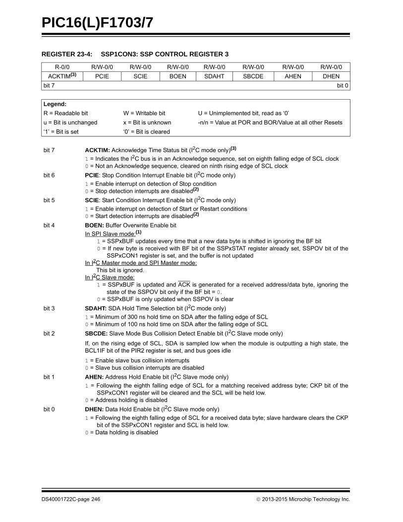
PIC16(L)F1703/7
REGISTER 23-4: SSP1CON3: SSP CONTROL REGISTER 3
R-0/0 R/W-0/0 R/W-0/0 R/W-0/0 R/W-0/0 R/W-0/0 R/W-0/0 R/W-0/0
ACKTIM(3) PCIE SCIE BOEN SDAHT SBCDE AHEN DHEN
bit 7 bit 0
Legend:
R = Readable bit W = Writable bit U = Unimplemented bit, read as ‘0’
u = Bit is unchanged x = Bit is unknown -n/n = Value at POR and BOR/Value at all other Resets
‘1’ = Bit is set ‘0’ = Bit is cleared
bit 7 ACKTIM: Acknowledge Time Status bit (I2C mode only)(3)
1 = Indicates the I2C bus is in an Acknowledge sequence, set on eighth falling edge of SCL clock0 = Not an Acknowledge sequence, cleared on ninth rising edge of SCL clock
bit 6 PCIE: Stop Condition Interrupt Enable bit (I2C mode only)
1 = Enable interrupt on detection of Stop condition0 = Stop detection interrupts are disabled(2)
bit 5 SCIE: Start Condition Interrupt Enable bit (I2C mode only)
1 = Enable interrupt on detection of Start or Restart conditions0 = Start detection interrupts are disabled(2)
bit 4 BOEN: Buffer Overwrite Enable bit
In SPI Slave mode:(1)
1 = SSPxBUF updates every time that a new data byte is shifted in ignoring the BF bit0 = If new byte is received with BF bit of the SSPxSTAT register already set, SSPOV bit of the
SSPxCON1 register is set, and the buffer is not updatedIn I2C Master mode and SPI Master mode:
This bit is ignored.In I2C Slave mode:
1 = SSPxBUF is updated and ACK is generated for a received address/data byte, ignoring thestate of the SSPOV bit only if the BF bit = 0.
0 = SSPxBUF is only updated when SSPOV is clear
bit 3 SDAHT: SDA Hold Time Selection bit (I2C mode only)
1 = Minimum of 300 ns hold time on SDA after the falling edge of SCL0 = Minimum of 100 ns hold time on SDA after the falling edge of SCL
bit 2 SBCDE: Slave Mode Bus Collision Detect Enable bit (I2C Slave mode only)
If, on the rising edge of SCL, SDA is sampled low when the module is outputting a high state, theBCL1IF bit of the PIR2 register is set, and bus goes idle
1 = Enable slave bus collision interrupts0 = Slave bus collision interrupts are disabled
bit 1 AHEN: Address Hold Enable bit (I2C Slave mode only)
1 = Following the eighth falling edge of SCL for a matching received address byte; CKP bit of theSSPxCON1 register will be cleared and the SCL will be held low.
0 = Address holding is disabled
bit 0 DHEN: Data Hold Enable bit (I2C Slave mode only)
1 = Following the eighth falling edge of SCL for a received data byte; slave hardware clears the CKPbit of the SSPxCON1 register and SCL is held low.
0 = Data holding is disabled
DS40001722C-page 246 2013-2015 Microchip Technology Inc.
PIC16(L)F1703/7
Note 1: For daisy-chained SPI operation; allows the user to ignore all but the last received byte. SSPOV is still set when a new byte is received and BF = 1, but hardware continues to write the most recent byte to SSPxBUF.
2: This bit has no effect in Slave modes that Start and Stop condition detection is explicitly listed as enabled.
3: The ACKTIM Status bit is only active when the AHEN bit or DHEN bit is set.
REGISTER 23-4: SSP1CON3: SSP CONTROL REGISTER 3 (CONTINUED)
2013-2015 Microchip Technology Inc. DS40001722C-page 247
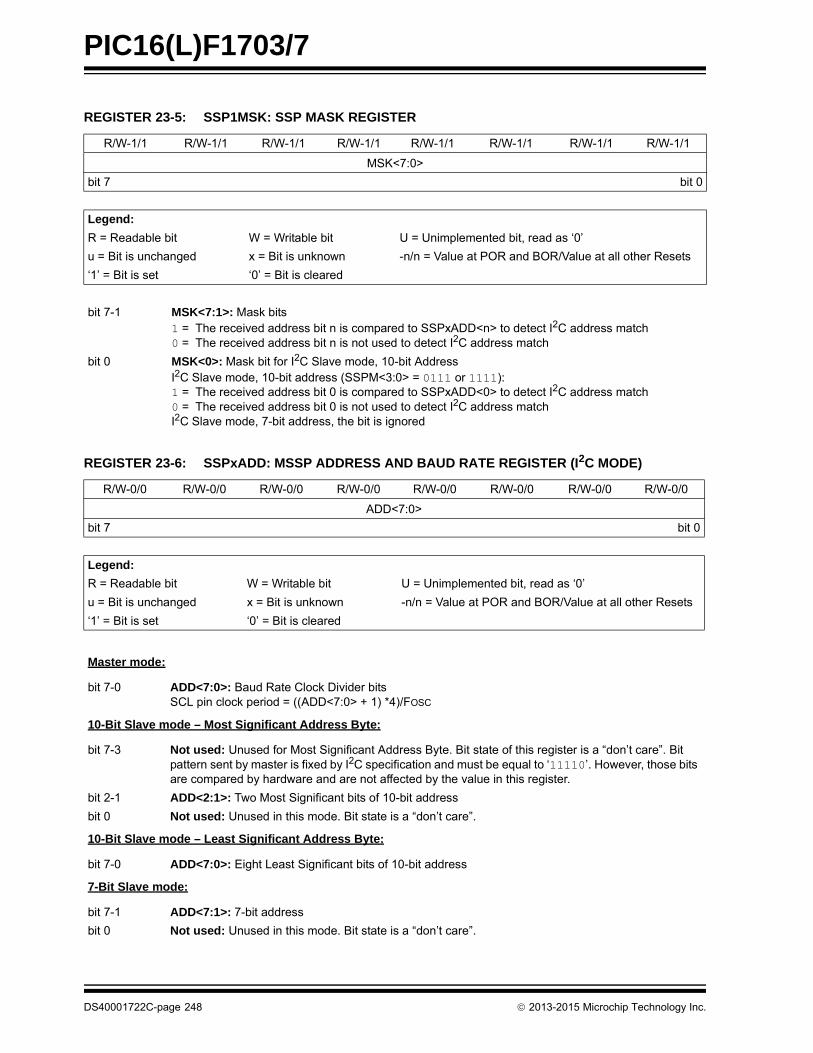
PIC16(L)F1703/7
REGISTER 23-5: SSP1MSK: SSP MASK REGISTER
R/W-1/1 R/W-1/1 R/W-1/1 R/W-1/1 R/W-1/1 R/W-1/1 R/W-1/1 R/W-1/1
MSK<7:0>
bit 7 bit 0
Legend:
R = Readable bit W = Writable bit U = Unimplemented bit, read as ‘0’
u = Bit is unchanged x = Bit is unknown -n/n = Value at POR and BOR/Value at all other Resets
‘1’ = Bit is set ‘0’ = Bit is cleared
bit 7-1 MSK<7:1>: Mask bits1 = The received address bit n is compared to SSPxADD<n> to detect I2C address match0 = The received address bit n is not used to detect I2C address match
bit 0 MSK<0>: Mask bit for I2C Slave mode, 10-bit AddressI2C Slave mode, 10-bit address (SSPM<3:0> = 0111 or 1111):1 = The received address bit 0 is compared to SSPxADD<0> to detect I2C address match0 = The received address bit 0 is not used to detect I2C address matchI2C Slave mode, 7-bit address, the bit is ignored
REGISTER 23-6: SSPxADD: MSSP ADDRESS AND BAUD RATE REGISTER (I2C MODE)
R/W-0/0 R/W-0/0 R/W-0/0 R/W-0/0 R/W-0/0 R/W-0/0 R/W-0/0 R/W-0/0
ADD<7:0>
bit 7 bit 0
Legend:
R = Readable bit W = Writable bit U = Unimplemented bit, read as ‘0’
u = Bit is unchanged x = Bit is unknown -n/n = Value at POR and BOR/Value at all other Resets
‘1’ = Bit is set ‘0’ = Bit is cleared
Master mode:
bit 7-0 ADD<7:0>: Baud Rate Clock Divider bitsSCL pin clock period = ((ADD<7:0> + 1) *4)/FOSC
10-Bit Slave mode – Most Significant Address Byte:
bit 7-3 Not used: Unused for Most Significant Address Byte. Bit state of this register is a “don’t care”. Bit pattern sent by master is fixed by I2C specification and must be equal to ‘11110’. However, those bits are compared by hardware and are not affected by the value in this register.
bit 2-1 ADD<2:1>: Two Most Significant bits of 10-bit address
bit 0 Not used: Unused in this mode. Bit state is a “don’t care”.
10-Bit Slave mode – Least Significant Address Byte:
bit 7-0 ADD<7:0>: Eight Least Significant bits of 10-bit address
7-Bit Slave mode:
bit 7-1 ADD<7:1>: 7-bit address
bit 0 Not used: Unused in this mode. Bit state is a “don’t care”.
DS40001722C-page 248 2013-2015 Microchip Technology Inc.
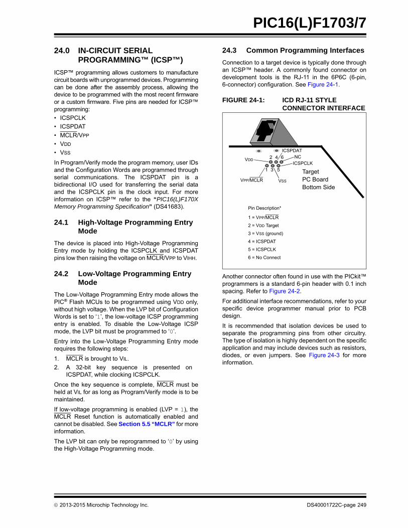
PIC16(L)F1703/7
24.0 IN-CIRCUIT SERIAL PROGRAMMING™ (ICSP™)
ICSP™ programming allows customers to manufacturecircuit boards with unprogrammed devices. Programmingcan be done after the assembly process, allowing thedevice to be programmed with the most recent firmwareor a custom firmware. Five pins are needed for ICSP™programming:
• ICSPCLK
• ICSPDAT
• MCLR/VPP
• VDD
• VSS
In Program/Verify mode the program memory, user IDsand the Configuration Words are programmed throughserial communications. The ICSPDAT pin is abidirectional I/O used for transferring the serial dataand the ICSPCLK pin is the clock input. For moreinformation on ICSP™ refer to the “PIC16(L)F170XMemory Programming Specification” (DS41683).
24.1 High-Voltage Programming Entry Mode
The device is placed into High-Voltage ProgrammingEntry mode by holding the ICSPCLK and ICSPDATpins low then raising the voltage on MCLR/VPP to VIHH.
24.2 Low-Voltage Programming Entry Mode
The Low-Voltage Programming Entry mode allows thePIC® Flash MCUs to be programmed using VDD only,without high voltage. When the LVP bit of ConfigurationWords is set to ‘1’, the low-voltage ICSP programmingentry is enabled. To disable the Low-Voltage ICSPmode, the LVP bit must be programmed to ‘0’.
Entry into the Low-Voltage Programming Entry moderequires the following steps:
1. MCLR is brought to VIL.
2. A 32-bit key sequence is presented onICSPDAT, while clocking ICSPCLK.
Once the key sequence is complete, MCLR must beheld at VIL for as long as Program/Verify mode is to bemaintained.
If low-voltage programming is enabled (LVP = 1), theMCLR Reset function is automatically enabled andcannot be disabled. See Section 5.5 “MCLR” for moreinformation.
The LVP bit can only be reprogrammed to ‘0’ by usingthe High-Voltage Programming mode.
24.3 Common Programming Interfaces
Connection to a target device is typically done throughan ICSP™ header. A commonly found connector ondevelopment tools is the RJ-11 in the 6P6C (6-pin,6-connector) configuration. See Figure 24-1.
FIGURE 24-1: ICD RJ-11 STYLE CONNECTOR INTERFACE
Another connector often found in use with the PICkit™programmers is a standard 6-pin header with 0.1 inchspacing. Refer to Figure 24-2.
For additional interface recommendations, refer to yourspecific device programmer manual prior to PCBdesign.
It is recommended that isolation devices be used toseparate the programming pins from other circuitry.The type of isolation is highly dependent on the specificapplication and may include devices such as resistors,diodes, or even jumpers. See Figure 24-3 for moreinformation.
1
2
3
4
5
6
Target
Bottom SidePC BoardVPP/MCLR VSS
ICSPCLKVDD
ICSPDATNC
Pin Description*
1 = VPP/MCLR
2 = VDD Target
3 = VSS (ground)
4 = ICSPDAT
5 = ICSPCLK
6 = No Connect
2013-2015 Microchip Technology Inc. DS40001722C-page 249
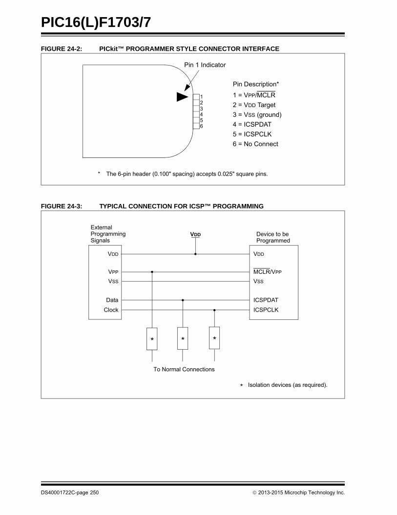
PIC16(L)F1703/7
FIGURE 24-2: PICkit™ PROGRAMMER STYLE CONNECTOR INTERFACE
FIGURE 24-3: TYPICAL CONNECTION FOR ICSP™ PROGRAMMING
123456
* The 6-pin header (0.100" spacing) accepts 0.025" square pins.
Pin Description*
1 = VPP/MCLR
2 = VDD Target
3 = VSS (ground)
4 = ICSPDAT
5 = ICSPCLK
6 = No Connect
Pin 1 Indicator
VDD
VPP
VSS
ExternalDevice to be
Data
Clock
VDD
MCLR/VPP
VSS
ICSPDAT
ICSPCLK
* **
To Normal Connections
* Isolation devices (as required).
Programming Signals Programmed
VDD
DS40001722C-page 250 2013-2015 Microchip Technology Inc.

PIC16(L)F1703/7
25.0 INSTRUCTION SET SUMMARY
Each instruction is a 14-bit word containing the opera-tion code (opcode) and all required operands. Theopcodes are broken into three broad categories.
• Byte Oriented
• Bit Oriented
• Literal and Control
The literal and control category contains the mostvaried instruction word format.
Table 25-3 lists the instructions recognized by theMPASMTM assembler.
All instructions are executed within a single instructioncycle, with the following exceptions, which may taketwo or three cycles:
• Subroutine takes two cycles (CALL, CALLW)• Returns from interrupts or subroutines take two
cycles (RETURN, RETLW, RETFIE)• Program branching takes two cycles (GOTO, BRA, BRW, BTFSS, BTFSC, DECFSZ, INCSFZ)
• One additional instruction cycle will be used when any instruction references an indirect file register and the file select register is pointing to program memory.
One instruction cycle consists of 4 oscillator cycles; foran oscillator frequency of 4 MHz, this gives a nominalinstruction execution rate of 1 MHz.
All instruction examples use the format ‘0xhh’ torepresent a hexadecimal number, where ‘h’ signifies ahexadecimal digit.
25.1 Read-Modify-Write Operations
Any instruction that specifies a file register as part ofthe instruction performs a Read-Modify-Write (R-M-W)operation. The register is read, the data is modified,and the result is stored according to either the instruc-tion, or the destination designator ‘d’. A read operationis performed on a register even if the instruction writesto that register.
TABLE 25-1: OPCODE FIELD DESCRIPTIONS
TABLE 25-2: ABBREVIATION DESCRIPTIONS
Field Description
f Register file address (0x00 to 0x7F)
W Working register (accumulator)
b Bit address within an 8-bit file register
k Literal field, constant data or label
x Don’t care location (= 0 or 1). The assembler will generate code with x = 0. It is the recommended form of use for compatibility with all Microchip software tools.
d Destination select; d = 0: store result in W,d = 1: store result in file register f. Default is d = 1.
n FSR or INDF number. (0-1)
mm Pre-post increment-decrement mode selection
Field Description
PC Program Counter
TO Time-Out bit
C Carry bit
DC Digit Carry bit
Z Zero bit
PD Power-Down bit
2013-2015 Microchip Technology Inc. DS40001722C-page 251

PIC16(L)F1703/7
FIGURE 25-1: GENERAL FORMAT FOR INSTRUCTIONS
Byte-oriented file register operations13 8 7 6 0
d = 0 for destination W
OPCODE d f (FILE #)
d = 1 for destination ff = 7-bit file register address
Bit-oriented file register operations13 10 9 7 6 0
OPCODE b (BIT #) f (FILE #)
b = 3-bit bit addressf = 7-bit file register address
Literal and control operations
13 8 7 0
OPCODE k (literal)
k = 8-bit immediate value
13 11 10 0
OPCODE k (literal)
k = 11-bit immediate value
General
CALL and GOTO instructions only
MOVLP instruction only
13 5 4 0
OPCODE k (literal)
k = 5-bit immediate value
MOVLB instruction only
13 9 8 0
OPCODE k (literal)
k = 9-bit immediate value
BRA instruction only
FSR Offset instructions
13 7 6 5 0
OPCODE n k (literal)
n = appropriate FSR
FSR Increment instructions
13 7 6 0
OPCODE k (literal)
k = 7-bit immediate value
13 3 2 1 0
OPCODE n m (mode)
n = appropriate FSRm = 2-bit mode value
k = 6-bit immediate value
13 0
OPCODE
OPCODE only
DS40001722C-page 252 2013-2015 Microchip Technology Inc.
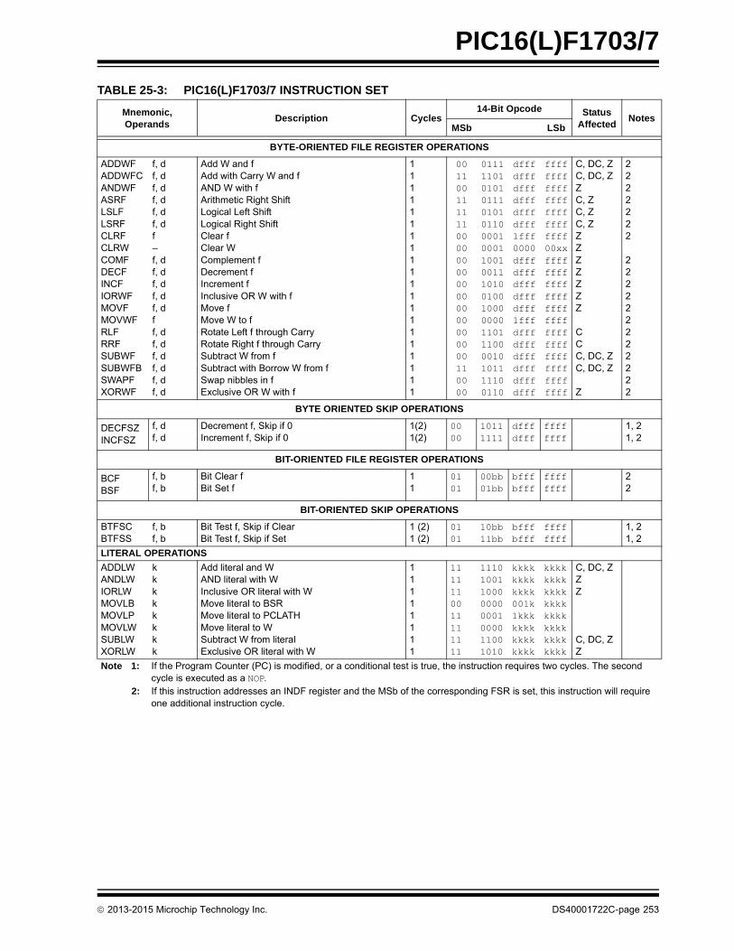
PIC16(L)F1703/7
TABLE 25-3: PIC16(L)F1703/7 INSTRUCTION SET
Mnemonic,Operands
Description Cycles14-Bit Opcode Status
AffectedNotes
MSb LSb
BYTE-ORIENTED FILE REGISTER OPERATIONS
ADDWFADDWFCANDWFASRFLSLFLSRFCLRFCLRWCOMFDECFINCFIORWFMOVFMOVWFRLFRRFSUBWFSUBWFBSWAPFXORWF
f, df, df, df, df, df, df–f, df, df, df, df, dff, df, df, df, df, df, d
Add W and fAdd with Carry W and fAND W with fArithmetic Right ShiftLogical Left ShiftLogical Right ShiftClear fClear WComplement fDecrement fIncrement fInclusive OR W with fMove fMove W to fRotate Left f through CarryRotate Right f through CarrySubtract W from fSubtract with Borrow W from fSwap nibbles in fExclusive OR W with f
11111111111111111111
0011001111110000000000000000000000110000
01111101010101110101011000010001100100111010010010000000110111000010101111100110
dfffdfffdfffdfffdfffdffflfff0000dfffdfffdfffdfffdfff1fffdfffdfffdfffdfffdfffdfff
ffffffffffffffffffffffffffff00xxffffffffffffffffffffffffffffffffffffffffffffffff
C, DC, ZC, DC, ZZC, ZC, ZC, ZZZZZZZZ
CCC, DC, ZC, DC, Z
Z
2222222
222222222222
BYTE ORIENTED SKIP OPERATIONS
DECFSZINCFSZ
f, df, d
Decrement f, Skip if 0Increment f, Skip if 0
1(2)1(2)
0000
10111111
dfffdfff
ffffffff
1, 21, 2
BIT-ORIENTED FILE REGISTER OPERATIONS
BCFBSF
f, bf, b
Bit Clear fBit Set f
11
0101
00bb01bb
bfffbfff
ffffffff
22
BIT-ORIENTED SKIP OPERATIONS
BTFSCBTFSS
f, bf, b
Bit Test f, Skip if ClearBit Test f, Skip if Set
1 (2)1 (2)
0101
10bb11bb
bfff bfff
ffffffff
1, 21, 2
LITERAL OPERATIONS
ADDLWANDLWIORLWMOVLBMOVLPMOVLWSUBLWXORLW
kkkkkkkk
Add literal and WAND literal with WInclusive OR literal with WMove literal to BSRMove literal to PCLATHMove literal to WSubtract W from literalExclusive OR literal with W
11111111
1111110011111111
11101001100000000001000011001010
kkkkkkkkkkkk001k1kkkkkkkkkkkkkkk
kkkkkkkkkkkkkkkkkkkkkkkkkkkkkkkk
C, DC, ZZZ
C, DC, ZZ
Note 1: If the Program Counter (PC) is modified, or a conditional test is true, the instruction requires two cycles. The second cycle is executed as a NOP.
2: If this instruction addresses an INDF register and the MSb of the corresponding FSR is set, this instruction will require one additional instruction cycle.
2013-2015 Microchip Technology Inc. DS40001722C-page 253
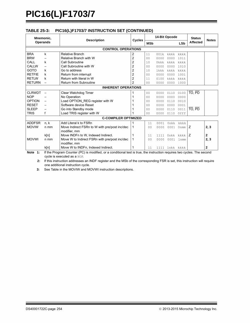
PIC16(L)F1703/7
TABLE 25-3: PIC16(L)F1703/7 INSTRUCTION SET (CONTINUED)
Mnemonic,Operands
Description Cycles14-Bit Opcode Status
AffectedNotes
MSb LSb
CONTROL OPERATIONS
BRABRWCALLCALLWGOTORETFIERETLWRETURN
k–k–kkk–
Relative BranchRelative Branch with WCall SubroutineCall Subroutine with WGo to addressReturn from interruptReturn with literal in WReturn from Subroutine
22222222
1100100010001100
001k00000kkk00001kkk000001000000
kkkk0000kkkk0000kkkk0000kkkk0000
kkkk1011kkkk1010kkkk1001kkkk1000
INHERENT OPERATIONS
CLRWDTNOPOPTIONRESETSLEEPTRIS
–––––f
Clear Watchdog TimerNo OperationLoad OPTION_REG register with WSoftware device ResetGo into Standby modeLoad TRIS register with W
111111
000000000000
000000000000000000000000
011000000110000001100110
010000000010000100110fff
TO, PD
TO, PD
C-COMPILER OPTIMIZED
ADDFSRMOVIW
MOVWI
n, kn mm
k[n]n mm
k[n]
Add Literal k to FSRnMove Indirect FSRn to W with pre/post inc/dec modifier, mmMove INDFn to W, Indexed Indirect.Move W to Indirect FSRn with pre/post inc/dec modifier, mmMove W to INDFn, Indexed Indirect.
11
11
1
1100
1100
11
00010000
11110000
1111
0nkk0001
0nkk0001
1nkk
kkkk0nmm
kkkk1nmm
kkkk
Z
Z
2, 3
22, 3
2
Note 1: If the Program Counter (PC) is modified, or a conditional test is true, the instruction requires two cycles. The second cycle is executed as a NOP.
2: If this instruction addresses an INDF register and the MSb of the corresponding FSR is set, this instruction will require one additional instruction cycle.
3: See Table in the MOVIW and MOVWI instruction descriptions.
DS40001722C-page 254 2013-2015 Microchip Technology Inc.
PIC16(L)F1703/7
25.2 Instruction Descriptions
ADDFSR Add Literal to FSRn
Syntax: [ label ] ADDFSR FSRn, k
Operands: -32 k 31n [ 0, 1]
Operation: FSR(n) + k FSR(n)
Status Affected: None
Description: The signed 6-bit literal ‘k’ is added to the contents of the FSRnH:FSRnL register pair.
FSRn is limited to the range 0000h-FFFFh. Moving beyond these bounds will cause the FSR to wrap-around.
ADDLW Add literal and W
Syntax: [ label ] ADDLW k
Operands: 0 k 255
Operation: (W) + k (W)
Status Affected: C, DC, Z
Description: The contents of the W register are added to the 8-bit literal ‘k’ and the result is placed in the W register.
ADDWF Add W and f
Syntax: [ label ] ADDWF f,d
Operands: 0 f 127d 0,1
Operation: (W) + (f) (destination)
Status Affected: C, DC, Z
Description: Add the contents of the W register with register ‘f’. If ‘d’ is ‘0’, the result is stored in the W register. If ‘d’ is ‘1’, the result is stored back in register ‘f’.
ADDWFC ADD W and CARRY bit to f
Syntax: [ label ] ADDWFC f {,d}
Operands: 0 f 127d [0,1]
Operation: (W) + (f) + (C) dest
Status Affected: C, DC, Z
Description: Add W, the Carry flag and data mem-ory location ‘f’. If ‘d’ is ‘0’, the result is placed in W. If ‘d’ is ‘1’, the result is placed in data memory location ‘f’.
ANDLW AND literal with W
Syntax: [ label ] ANDLW k
Operands: 0 k 255
Operation: (W) .AND. (k) (W)
Status Affected: Z
Description: The contents of W register are AND’ed with the 8-bit literal ‘k’. The result is placed in the W register.
ANDWF AND W with f
Syntax: [ label ] ANDWF f,d
Operands: 0 f 127d 0,1
Operation: (W) .AND. (f) (destination)
Status Affected: Z
Description: AND the W register with register ‘f’. If ‘d’ is ‘0’, the result is stored in the W register. If ‘d’ is ‘1’, the result is stored back in register ‘f’.
ASRF Arithmetic Right Shift
Syntax: [ label ] ASRF f {,d}
Operands: 0 f 127d [0,1]
Operation: (f<7>) dest<7>(f<7:1>) dest<6:0>,(f<0>) C,
Status Affected: C, Z
Description: The contents of register ‘f’ are shifted one bit to the right through the Carry flag. The MSb remains unchanged. If ‘d’ is ‘0’, the result is placed in W. If ‘d’ is ‘1’, the result is stored back in register ‘f’.
register f C
2013-2015 Microchip Technology Inc. DS40001722C-page 255
PIC16(L)F1703/7
BCF Bit Clear f
Syntax: [ label ] BCF f,b
Operands: 0 f 1270 b 7
Operation: 0 (f<b>)
Status Affected: None
Description: Bit ‘b’ in register ‘f’ is cleared.
BRA Relative Branch
Syntax: [ label ] BRA label [ label ] BRA $+k
Operands: -256 label - PC + 1 255-256 k 255
Operation: (PC) + 1 + k PC
Status Affected: None
Description: Add the signed 9-bit literal ‘k’ to the PC. Since the PC will have incremented to fetch the next instruction, the new address will be PC + 1 + k. This instruction is a 2-cycle instruction. This branch has a limited range.
BRW Relative Branch with W
Syntax: [ label ] BRW
Operands: None
Operation: (PC) + (W) PC
Status Affected: None
Description: Add the contents of W (unsigned) to the PC. Since the PC will have incremented to fetch the next instruction, the new address will be PC + 1 + (W). This instruction is a 2-cycle instruction.
BSF Bit Set f
Syntax: [ label ] BSF f,b
Operands: 0 f 1270 b 7
Operation: 1 (f<b>)
Status Affected: None
Description: Bit ‘b’ in register ‘f’ is set.
BTFSC Bit Test f, Skip if Clear
Syntax: [ label ] BTFSC f,b
Operands: 0 f 1270 b 7
Operation: skip if (f<b>) = 0
Status Affected: None
Description: If bit ‘b’ in register ‘f’ is ‘1’, the next instruction is executed.If bit ‘b’, in register ‘f’, is ‘0’, the next instruction is discarded, and a NOP is executed instead, making this a 2-cycle instruction.
BTFSS Bit Test f, Skip if Set
Syntax: [ label ] BTFSS f,b
Operands: 0 f 1270 b < 7
Operation: skip if (f<b>) = 1
Status Affected: None
Description: If bit ‘b’ in register ‘f’ is ‘0’, the next instruction is executed.If bit ‘b’ is ‘1’, then the next instruction is discarded and a NOP is executed instead, making this a 2-cycle instruction.
DS40001722C-page 256 2013-2015 Microchip Technology Inc.

PIC16(L)F1703/7
CALL Call Subroutine
Syntax: [ label ] CALL k
Operands: 0 k 2047
Operation: (PC)+ 1 TOS,k PC<10:0>,(PCLATH<6:3>) PC<14:11>
Status Affected: None
Description: Call Subroutine. First, return address (PC + 1) is pushed onto the stack. The 11-bit immediate address is loaded into PC bits <10:0>. The upper bits of the PC are loaded from PCLATH. CALL is a 2-cycle instruction.
CALLW Subroutine Call With W
Syntax: [ label ] CALLW
Operands: None
Operation: (PC) +1 TOS,(W) PC<7:0>,(PCLATH<6:0>) PC<14:8>
Status Affected: None
Description: Subroutine call with W. First, the return address (PC + 1) is pushed onto the return stack. Then, the contents of W is loaded into PC<7:0>, and the contents of PCLATH into PC<14:8>. CALLW is a 2-cycle instruction.
CLRF Clear f
Syntax: [ label ] CLRF f
Operands: 0 f 127
Operation: 00h (f)1 Z
Status Affected: Z
Description: The contents of register ‘f’ are cleared and the Z bit is set.
CLRW Clear W
Syntax: [ label ] CLRW
Operands: None
Operation: 00h (W)1 Z
Status Affected: Z
Description: W register is cleared. Zero bit (Z) is set.
CLRWDT Clear Watchdog Timer
Syntax: [ label ] CLRWDT
Operands: None
Operation: 00h WDT0 WDT prescaler,1 TO1 PD
Status Affected: TO, PD
Description: CLRWDT instruction resets the Watch-dog Timer. It also resets the prescaler of the WDT. Status bits TO and PD are set.
COMF Complement f
Syntax: [ label ] COMF f,d
Operands: 0 f 127d [0,1]
Operation: (f) (destination)
Status Affected: Z
Description: The contents of register ‘f’ are complemented. If ‘d’ is ‘0’, the result is stored in W. If ‘d’ is ‘1’, the result is stored back in register ‘f’.
DECF Decrement f
Syntax: [ label ] DECF f,d
Operands: 0 f 127d [0,1]
Operation: (f) - 1 (destination)
Status Affected: Z
Description: Decrement register ‘f’. If ‘d’ is ‘0’, the result is stored in the W register. If ‘d’ is ‘1’, the result is stored back in register ‘f’.
2013-2015 Microchip Technology Inc. DS40001722C-page 257
PIC16(L)F1703/7
DECFSZ Decrement f, Skip if 0
Syntax: [ label ] DECFSZ f,d
Operands: 0 f 127d [0,1]
Operation: (f) - 1 (destination); skip if result = 0
Status Affected: None
Description: The contents of register ‘f’ are decre-mented. If ‘d’ is ‘0’, the result is placed in the W register. If ‘d’ is ‘1’, the result is placed back in register ‘f’. If the result is ‘1’, the next instruction is executed. If the result is ‘0’, then a NOP is executed instead, making it a 2-cycle instruction.
GOTO Unconditional Branch
Syntax: [ label ] GOTO k
Operands: 0 k 2047
Operation: k PC<10:0>PCLATH<6:3> PC<14:11>
Status Affected: None
Description: GOTO is an unconditional branch. The 11-bit immediate value is loaded into PC bits <10:0>. The upper bits of PC are loaded from PCLATH<4:3>. GOTO is a 2-cycle instruction.
INCF Increment f
Syntax: [ label ] INCF f,d
Operands: 0 f 127d [0,1]
Operation: (f) + 1 (destination)
Status Affected: Z
Description: The contents of register ‘f’ are incre-mented. If ‘d’ is ‘0’, the result is placed in the W register. If ‘d’ is ‘1’, the result is placed back in register ‘f’.
INCFSZ Increment f, Skip if 0
Syntax: [ label ] INCFSZ f,d
Operands: 0 f 127d [0,1]
Operation: (f) + 1 (destination), skip if result = 0
Status Affected: None
Description: The contents of register ‘f’ are incre-mented. If ‘d’ is ‘0’, the result is placed in the W register. If ‘d’ is ‘1’, the result is placed back in register ‘f’.If the result is ‘1’, the next instruction is executed. If the result is ‘0’, a NOP is executed instead, making it a 2-cycle instruction.
IORLW Inclusive OR literal with W
Syntax: [ label ] IORLW k
Operands: 0 k 255
Operation: (W) .OR. k (W)
Status Affected: Z
Description: The contents of the W register are OR’ed with the 8-bit literal ‘k’. The result is placed in the W register.
IORWF Inclusive OR W with f
Syntax: [ label ] IORWF f,d
Operands: 0 f 127d [0,1]
Operation: (W) .OR. (f) (destination)
Status Affected: Z
Description: Inclusive OR the W register with regis-ter ‘f’. If ‘d’ is ‘0’, the result is placed in the W register. If ‘d’ is ‘1’, the result is placed back in register ‘f’.
DS40001722C-page 258 2013-2015 Microchip Technology Inc.

PIC16(L)F1703/7
LSLF Logical Left Shift
Syntax: [ label ] LSLF f {,d}
Operands: 0 f 127d [0,1]
Operation: (f<7>) C(f<6:0>) dest<7:1>0 dest<0>
Status Affected: C, Z
Description: The contents of register ‘f’ are shifted one bit to the left through the Carry flag. A ‘0’ is shifted into the LSb. If ‘d’ is ‘0’, the result is placed in W. If ‘d’ is ‘1’, the result is stored back in register ‘f’.
LSRF Logical Right Shift
Syntax: [ label ] LSRF f {,d}
Operands: 0 f 127d [0,1]
Operation: 0 dest<7>(f<7:1>) dest<6:0>,(f<0>) C,
Status Affected: C, Z
Description: The contents of register ‘f’ are shifted one bit to the right through the Carry flag. A ‘0’ is shifted into the MSb. If ‘d’ is ‘0’, the result is placed in W. If ‘d’ is ‘1’, the result is stored back in register ‘f’.
register f 0C
register f C0
MOVF Move f
Syntax: [ label ] MOVF f,d
Operands: 0 f 127d [0,1]
Operation: (f) (dest)
Status Affected: Z
Description: The contents of register f is moved to a destination dependent upon the status of d. If d = 0, destination is W register. If d = 1, the destination is file register f itself. d = 1 is useful to test a file register since status flag Z is affected.
Words: 1
Cycles: 1
Example: MOVF FSR, 0
After InstructionW = value in FSR registerZ = 1
2013-2015 Microchip Technology Inc. DS40001722C-page 259
PIC16(L)F1703/7
MOVIW Move INDFn to W
Syntax: [ label ] MOVIW ++FSRn[ label ] MOVIW --FSRn[ label ] MOVIW FSRn++[ label ] MOVIW FSRn--[ label ] MOVIW k[FSRn]
Operands: n [0,1]mm [00,01, 10, 11]-32 k 31
Operation: INDFn WEffective address is determined by• FSR + 1 (preincrement)• FSR - 1 (predecrement)• FSR + k (relative offset)After the Move, the FSR value will be either:• FSR + 1 (all increments)• FSR - 1 (all decrements)• Unchanged
Status Affected: Z
Mode Syntax mm
Preincrement ++FSRn 00
Predecrement --FSRn 01
Postincrement FSRn++ 10
Postdecrement FSRn-- 11
Description: This instruction is used to move data between W and one of the indirect registers (INDFn). Before/after this move, the pointer (FSRn) is updated by pre/post incrementing/decrementing it.
Note: The INDFn registers are not physical registers. Any instruction that accesses an INDFn register actually accesses the register at the address specified by the FSRn.
FSRn is limited to the range 0000h - FFFFh. Incrementing/decrementing it beyond these bounds will cause it to wrap-around.
MOVLB Move literal to BSR
Syntax: [ label ] MOVLB k
Operands: 0 k 31
Operation: k BSR
Status Affected: None
Description: The 5-bit literal ‘k’ is loaded into the Bank Select Register (BSR).
MOVLP Move literal to PCLATH
Syntax: [ label ] MOVLP k
Operands: 0 k 127
Operation: k PCLATH
Status Affected: None
Description: The 7-bit literal ‘k’ is loaded into the PCLATH register.
MOVLW Move literal to W
Syntax: [ label ] MOVLW k
Operands: 0 k 255
Operation: k (W)
Status Affected: None
Description: The 8-bit literal ‘k’ is loaded into W reg-ister. The “don’t cares” will assemble as ‘0’s.
Words: 1
Cycles: 1
Example: MOVLW 0x5A
After InstructionW = 0x5A
MOVWF Move W to f
Syntax: [ label ] MOVWF f
Operands: 0 f 127
Operation: (W) (f)
Status Affected: None
Description: Move data from W register to register ‘f’.
Words: 1
Cycles: 1
Example: MOVWF OPTION_REG
Before InstructionOPTION_REG = 0xFF
W = 0x4FAfter Instruction
OPTION_REG = 0x4F W = 0x4F
DS40001722C-page 260 2013-2015 Microchip Technology Inc.
PIC16(L)F1703/7
MOVWI Move W to INDFn
Syntax: [ label ] MOVWI ++FSRn[ label ] MOVWI --FSRn[ label ] MOVWI FSRn++[ label ] MOVWI FSRn--[ label ] MOVWI k[FSRn]
Operands: n [0,1]mm [00,01, 10, 11]-32 k 31
Operation: W INDFnEffective address is determined by• FSR + 1 (preincrement)• FSR - 1 (predecrement)• FSR + k (relative offset)After the Move, the FSR value will be either:• FSR + 1 (all increments)• FSR - 1 (all decrements)Unchanged
Status Affected: None
Mode Syntax mm
Preincrement ++FSRn 00
Predecrement --FSRn 01
Postincrement FSRn++ 10
Postdecrement FSRn-- 11
Description: This instruction is used to move data between W and one of the indirect registers (INDFn). Before/after this move, the pointer (FSRn) is updated by pre/post incrementing/decrementing it.
Note: The INDFn registers are not physical registers. Any instruction that accesses an INDFn register actually accesses the register at the address specified by the FSRn.
FSRn is limited to the range 0000h-FFFFh. Incrementing/decrementing it beyond these bounds will cause it to wrap-around.
The increment/decrement operation on FSRn WILL NOT affect any Status bits.
NOP No Operation
Syntax: [ label ] NOP
Operands: None
Operation: No operation
Status Affected: None
Description: No operation.
Words: 1
Cycles: 1
Example: NOP
OPTIONLoad OPTION_REG Register with W
Syntax: [ label ] OPTION
Operands: None
Operation: (W) OPTION_REG
Status Affected: None
Description: Move data from W register to OPTION_REG register.
Words: 1
Cycles: 1
Example: OPTION
Before InstructionOPTION_REG = 0xFF
W = 0x4FAfter Instruction
OPTION_REG = 0x4F W = 0x4F
RESET Software Reset
Syntax: [ label ] RESET
Operands: None
Operation: Execute a device Reset. Resets the RI flag of the PCON register.
Status Affected: None
Description: This instruction provides a way to execute a hardware Reset by software.
2013-2015 Microchip Technology Inc. DS40001722C-page 261
PIC16(L)F1703/7
RETFIE Return from Interrupt
Syntax: [ label ] RETFIE k
Operands: None
Operation: TOS PC,1 GIE
Status Affected: None
Description: Return from Interrupt. Stack is POPed and Top-of-Stack (TOS) is loaded in the PC. Interrupts are enabled by setting Global Interrupt Enable bit, GIE (INTCON<7>). This is a 2-cycle instruction.
Words: 1
Cycles: 2
Example: RETFIE
After InterruptPC = TOSGIE = 1
RETLW Return with literal in W
Syntax: [ label ] RETLW k
Operands: 0 k 255
Operation: k (W); TOS PC
Status Affected: None
Description: The W register is loaded with the 8-bit literal ‘k’. The program counter is loaded from the top of the stack (the return address). This is a 2-cycle instruction.
Words: 1
Cycles: 2
Example:
TABLE
CALL TABLE;W contains table;offset value
• ;W now has table value••ADDWF PC ;W = offsetRETLW k1 ;Begin tableRETLW k2 ;•••RETLW kn ; End of table
Before InstructionW = 0x07
After InstructionW = value of k8
RETURN Return from Subroutine
Syntax: [ label ] RETURN
Operands: None
Operation: TOS PC
Status Affected: None
Description: Return from subroutine. The stack is POPed and the top of the stack (TOS) is loaded into the program counter. This is a 2-cycle instruction.
RLF Rotate Left f through Carry
Syntax: [ label ] RLF f,d
Operands: 0 f 127d [0,1]
Operation: See description below
Status Affected: C
Description: The contents of register ‘f’ are rotated one bit to the left through the Carry flag. If ‘d’ is ‘0’, the result is placed in the W register. If ‘d’ is ‘1’, the result is stored back in register ‘f’.
Words: 1
Cycles: 1
Example: RLF REG1,0
Before InstructionREG1 = 1110 0110C = 0
After InstructionREG1 = 1110 0110W = 1100 1100C = 1
Register fC
DS40001722C-page 262 2013-2015 Microchip Technology Inc.

PIC16(L)F1703/7
RRF Rotate Right f through Carry
Syntax: [ label ] RRF f,d
Operands: 0 f 127d [0,1]
Operation: See description below
Status Affected: C
Description: The contents of register ‘f’ are rotated one bit to the right through the Carry flag. If ‘d’ is ‘0’, the result is placed in the W register. If ‘d’ is ‘1’, the result is placed back in register ‘f’.
SLEEP Enter Sleep mode
Syntax: [ label ] SLEEP
Operands: None
Operation: 00h WDT,0 WDT prescaler,1 TO,0 PD
Status Affected: TO, PD
Description: The power-down Status bit, PD is cleared. Time-out Status bit, TO is set. Watchdog Timer and its prescaler are cleared.The processor is put into Sleep mode with the oscillator stopped.
Register fC
SUBLW Subtract W from literal
Syntax: [ label ] SUBLW k
Operands: 0 k 255
Operation: k - (W) W)
Status Affected: C, DC, Z
Description: The W register is subtracted (2’s complement method) from the 8-bit literal ‘k’. The result is placed in the W register.
SUBWF Subtract W from f
Syntax: [ label ] SUBWF f,d
Operands: 0 f 127d [0,1]
Operation: (f) - (W) destination)
Status Affected: C, DC, Z
Description: Subtract (2’s complement method) W register from register ‘f’. If ‘d’ is ‘0’, the result is stored in the W register. If ‘d’ is ‘1’, the result is stored back in register ‘f.
SUBWFB Subtract W from f with Borrow
Syntax: SUBWFB f {,d}
Operands: 0 f 127d [0,1]
Operation: (f) – (W) – (B) dest
Status Affected: C, DC, Z
Description: Subtract W and the BORROW flag (CARRY) from register ‘f’ (2’s complement method). If ‘d’ is ‘0’, the result is stored in W. If ‘d’ is ‘1’, the result is stored back in register ‘f’.
C = 0 W k
C = 1 W k
DC = 0 W<3:0> k<3:0>
DC = 1 W<3:0> k<3:0>
C = 0 W f
C = 1 W f
DC = 0 W<3:0> f<3:0>
DC = 1 W<3:0> f<3:0>
2013-2015 Microchip Technology Inc. DS40001722C-page 263
PIC16(L)F1703/7
SWAPF Swap Nibbles in f
Syntax: [ label ] SWAPF f,d
Operands: 0 f 127d [0,1]
Operation: (f<3:0>) (destination<7:4>),(f<7:4>) (destination<3:0>)
Status Affected: None
Description: The upper and lower nibbles of register ‘f’ are exchanged. If ‘d’ is ‘0’, the result is placed in the W register. If ‘d’ is ‘1’, the result is placed in register ‘f’.
TRIS Load TRIS Register with W
Syntax: [ label ] TRIS f
Operands: 5 f 7
Operation: (W) TRIS register ‘f’
Status Affected: None
Description: Move data from W register to TRIS register.When ‘f’ = 5, TRISA is loaded.When ‘f’ = 6, TRISB is loaded.When ‘f’ = 7, TRISC is loaded.
XORLW Exclusive OR literal with W
Syntax: [ label ] XORLW k
Operands: 0 k 255
Operation: (W) .XOR. k W)
Status Affected: Z
Description: The contents of the W register are XOR’ed with the 8-bit literal ‘k’. The result is placed in the W register.
XORWF Exclusive OR W with f
Syntax: [ label ] XORWF f,d
Operands: 0 f 127d [0,1]
Operation: (W) .XOR. (f) destination)
Status Affected: Z
Description: Exclusive OR the contents of the W register with register ‘f’. If ‘d’ is ‘0’, the result is stored in the W register. If ‘d’ is ‘1’, the result is stored back in register ‘f’.
DS40001722C-page 264 2013-2015 Microchip Technology Inc.

PIC16(L)F1703/7
26.0 ELECTRICAL SPECIFICATIONS
26.1 Absolute Maximum Ratings(†)
Ambient temperature under bias...................................................................................................... -40°C to +125°C
Storage temperature ........................................................................................................................ -65°C to +150°C
Voltage on pins with respect to VSS
on VDD pin
PIC16F1703/7 ........................................................................................................... -0.3V to +6.5V
PIC16LF1703/7 ......................................................................................................... -0.3V to +4.0V
on MCLR pin ........................................................................................................................... -0.3V to +9.0V
on all other pins ............................................................................................................ -0.3V to (VDD + 0.3V)
Maximum current
on VSS pin(1)
-40°C TA +85°C .............................................................................................................. 250 mA
+85°C TA +125°C ............................................................................................................. 85 mA
on VDD pin(1)
-40°C TA +85°C .............................................................................................................. 250 mA
+85°C TA +125°C ............................................................................................................. 85 mA
sunk by any I/O pin ............................................................................................................................... 50 mA
sourced by any I/O pin ........................................................................................................................... 50 mA
sourced by any Op Amp output pin ...................................................................................................... 100 mA
Clamp current, IK (VPIN < 0 or VPIN > VDD) ................................................................................................... 20 mA
Total power dissipation(2) ............................................................................................................................. 800 mW
Note 1: Maximum current rating requires even load distribution across I/O pins. Maximum current rating may be limited by the device package power dissipation characterizations, see Table 26-6 to calculate device specifications.
2: Power dissipation is calculated as follows: PDIS = VDD x {IDD – IOH} + {(VDD – VOH) x IOH} + (VOl x IOL).
† NOTICE: Stresses above those listed under “Absolute Maximum Ratings” may cause permanent damage to thedevice. This is a stress rating only and functional operation of the device at those or any other conditions above thoseindicated in the operation listings of this specification is not implied. Exposure above maximum rating conditions forextended periods may affect device reliability.
2013-2015 Microchip Technology Inc. DS40001722C-page 265

PIC16(L)F1703/7
26.2 Standard Operating Conditions
The standard operating conditions for any device are defined as:
Operating Voltage: VDDMIN VDD VDDMAX
Operating Temperature: TA_MIN TA TA_MAX
VDD — Operating Supply Voltage(1)
PIC16LF1703/7
VDDMIN (Fosc 16 MHz).......................................................................................................... +1.8V
VDDMIN (Fosc 16 MHz).......................................................................................................... +2.5V
VDDMAX .................................................................................................................................... +3.6V
PIC16F1703/7
VDDMIN (Fosc 16 MHz).......................................................................................................... +2.3V
VDDMIN (Fosc 16 MHz).......................................................................................................... +2.5V
VDDMAX .................................................................................................................................... +5.5V
TA — Operating Ambient Temperature Range
Industrial Temperature
TA_MIN ...................................................................................................................................... -40°C
TA_MAX .................................................................................................................................... +85°C
Extended Temperature
TA_MIN ...................................................................................................................................... -40°C
TA_MAX .................................................................................................................................. +125°C
Note 1: See Parameter D001, DS Characteristics: Supply Voltage.
DS40001722C-page 266 2013-2015 Microchip Technology Inc.
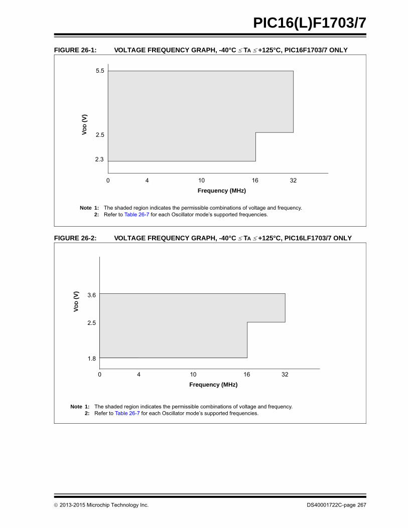
PIC16(L)F1703/7
FIGURE 26-1: VOLTAGE FREQUENCY GRAPH, -40°C TA +125°C, PIC16F1703/7 ONLY
FIGURE 26-2: VOLTAGE FREQUENCY GRAPH, -40°C TA +125°C, PIC16LF1703/7 ONLY
0
2.5
Frequency (MHz)
VD
D (
V)
Note 1: The shaded region indicates the permissible combinations of voltage and frequency.2: Refer to Table 26-7 for each Oscillator mode’s supported frequencies.
4 3210 16
5.5
2.3
1.8
0
2.5
Frequency (MHz)
VD
D (
V)
Note 1: The shaded region indicates the permissible combinations of voltage and frequency.2: Refer to Table 26-7 for each Oscillator mode’s supported frequencies.
4 3210 16
3.6
2013-2015 Microchip Technology Inc. DS40001722C-page 267
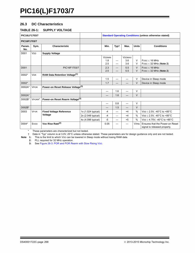
PIC16(L)F1703/7
eset
.
26.3 DC Characteristics
TABLE 26-1: SUPPLY VOLTAGE
PIC16LF1703/7 Standard Operating Conditions (unless otherwise stated)
PIC16F1703/7
Param. No.
Sym. Characteristic Min. Typ† Max. Units Conditions
D001 VDD Supply Voltage
VDDMIN
1.82.5
——
VDDMAX
3.63.6
VV
FOSC 16 MHzFOSC 32 MHz (Note 2)
D001 PIC16F1703/7 2.32.5
——
5.55.5
VV
FOSC 16 MHz:FOSC 32 MHz (Note 2)
D002* VDR RAM Data Retention Voltage(1)
1.5 — — V Device in Sleep mode
D002* 1.7 — — V Device in Sleep mode
D002A* VPOR Power-on Reset Release Voltage(3)
— 1.6 — V
D002A* — 1.6 — V
D002B* VPORR* Power-on Reset Rearm Voltage(3)
— 0.8 — V
D002B* — 1.5 — V
D003 VFVR Fixed Voltage Reference Voltage
1x (1.024 typical) -4 — +4 % VDD 2.5V, -40°C to +85°C
2x (2.048 typical) -4 — +4 % VDD 2.5V, -40°C to +85°C
4x (4.096 typical) -5 — +5 % VDD 4.75V, -40°C to +85°C
D004* SVDD VDD Rise Rate(2) 0.05 — — V/ms Ensures that the Power-on Rsignal is released properly.
* These parameters are characterized but not tested.† Data in “Typ” column is at 3.0V, 25°C unless otherwise stated. These parameters are for design guidance only and are not tested
Note 1: This is the limit to which VDD can be lowered in Sleep mode without losing RAM data.2: PLL required for 32 MHz operation.3: See Figure 26-3: POR and POR Rearm with Slow Rising VDD.
DS40001722C-page 268 2013-2015 Microchip Technology Inc.

PIC16(L)F1703/7
FIGURE 26-3: POR AND POR REARM WITH SLOW RISING VDD
VDD
VPOR
VPORR
VSS
VSS
NPOR(1)
TPOR(3)
POR REARM
Note 1: When NPOR is low, the device is held in Reset.2: TPOR 1 s typical.3: TVLOW 2.7 s typical.
TVLOW(2)
SVDD
2013-2015 Microchip Technology Inc. DS40001722C-page 269
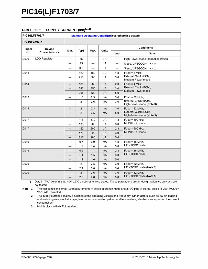
PIC16(L)F1703/7
TABLE 26-2: SUPPLY CURRENT (IDD)(1,2)
PIC16LF1703/7 (unless otherwise stated)
PIC16F1703/7
ParamNo.
Device Characteristics
Min. Typ† Max. UnitsConditions
VDD Note
D009 LDO Regulator — 75 — A — High-Power mode, normal operation
— 15 — A — Sleep, VREGCON<1> = 0
— 0.3 — A — Sleep, VREGCON<1> = 1
D014 — 120 180 A 1.8 FOSC = 4 MHz,External Clock (ECM),Medium-Power mode
— 210 300 A 3.0
D014 — 185 280 A 2.3 FOSC = 4 MHz,External Clock (ECM),Medium-Power mode
— 245 350 A 3.0
— 305 420 A 5.0
D015 — 1.6 2.3 mA 3.0 FOSC = 32 MHz,External Clock (ECH),High-Power mode (Note 3)
— 2 2.6 mA 3.6
D015 — 2 2.3 mA 3.0 FOSC = 32 MHz,External Clock (ECH),High-Power mode (Note 3)
— 2 2.5 mA 5.0
D017 — 115 170 A 1.8 FOSC = 500 kHz,MFINTOSC mode— 135 200 A 3.0
D017 — 150 200 A 2.3 FOSC = 500 kHz,MFINTOSC mode— 170 220 A 3.0
— 215 280 A 5.0
D019 — 0.7 0.9 mA 1.8 FOSC = 16 MHz,HFINTOSC mode— 1.2 1.4 mA 3.0
D019 — 0.9 1.1 mA 2.3 FOSC = 16 MHz,HFINTOSC mode— 1.1 1.5 mA 3.0
— 1.2 1.6 mA 5.0
D020 — 2 2.5 mA 3.0 FOSC = 32 MHz,HFINTOSC mode (Note 3)— 2.4 3.0 mA 3.6
D020 — 2 2.6 mA 3.0 FOSC = 32 MHz,HFINTOSC mode (Note 3)— 2.2 2.8 mA 5.0
† Data in “Typ” column is at 3.0V, 25°C unless otherwise stated. These parameters are for design guidance only and are not tested.
Note 1: The test conditions for all IDD measurements in active operation mode are: all I/O pins tri-stated, pulled to VDD; MCLR = VDD; WDT disabled.
2: The supply current is mainly a function of the operating voltage and frequency. Other factors, such as I/O pin loading and switching rate, oscillator type, internal code execution pattern and temperature, also have an impact on the current consumption.
3: 8 MHz clock with 4x PLL enabled.
Standard Operating Conditions
DS40001722C-page 270 2013-2015 Microchip Technology Inc.
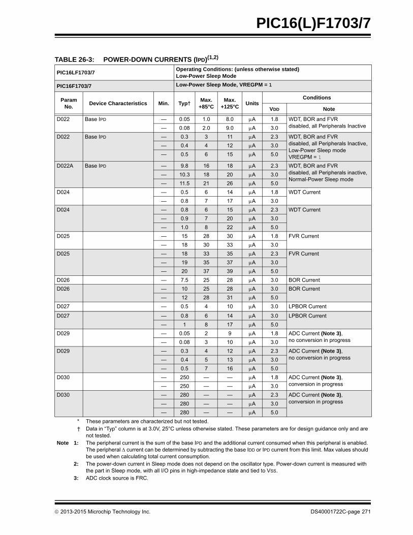
PIC16(L)F1703/7
TABLE 26-3: POWER-DOWN CURRENTS (IPD)(1,2)
PIC16LF1703/7Operating Conditions: (unless otherwise stated)Low-Power Sleep Mode
PIC16F1703/7 Low-Power Sleep Mode, VREGPM = 1
ParamNo.
Device Characteristics Min. Typ†Max.
+85°CMax.
+125°CUnits
Conditions
VDD Note
D022 Base IPD — 0.05 1.0 8.0 A 1.8 WDT, BOR and FVRdisabled, all Peripherals Inactive— 0.08 2.0 9.0 A 3.0
D022 Base IPD — 0.3 3 11 A 2.3 WDT, BOR and FVRdisabled, all Peripherals Inactive,Low-Power Sleep modeVREGPM = 1
— 0.4 4 12 A 3.0
— 0.5 6 15 A 5.0
D022A Base IPD — 9.8 16 18 A 2.3 WDT, BOR and FVRdisabled, all Peripherals inactive,Normal-Power Sleep mode
— 10.3 18 20 A 3.0
— 11.5 21 26 A 5.0
D024 — 0.5 6 14 A 1.8 WDT Current
— 0.8 7 17 A 3.0
D024 — 0.8 6 15 A 2.3 WDT Current
— 0.9 7 20 A 3.0
— 1.0 8 22 A 5.0
D025 — 15 28 30 A 1.8 FVR Current
— 18 30 33 A 3.0
D025 — 18 33 35 A 2.3 FVR Current
— 19 35 37 A 3.0
— 20 37 39 A 5.0
D026 — 7.5 25 28 A 3.0 BOR Current
D026 — 10 25 28 A 3.0 BOR Current
— 12 28 31 A 5.0
D027 — 0.5 4 10 A 3.0 LPBOR Current
D027 — 0.8 6 14 A 3.0 LPBOR Current
— 1 8 17 A 5.0
D029 — 0.05 2 9 A 1.8 ADC Current (Note 3), no conversion in progress— 0.08 3 10 A 3.0
D029 — 0.3 4 12 A 2.3 ADC Current (Note 3), no conversion in progress— 0.4 5 13 A 3.0
— 0.5 7 16 A 5.0
D030 — 250 — — A 1.8 ADC Current (Note 3), conversion in progress— 250 — — A 3.0
D030 — 280 — — A 2.3 ADC Current (Note 3), conversion in progress— 280 — — A 3.0
— 280 — — A 5.0
* These parameters are characterized but not tested.† Data in “Typ” column is at 3.0V, 25°C unless otherwise stated. These parameters are for design guidance only and are
not tested.Note 1: The peripheral current is the sum of the base IPD and the additional current consumed when this peripheral is enabled.
The peripheral current can be determined by subtracting the base IDD or IPD current from this limit. Max values should be used when calculating total current consumption.
2: The power-down current in Sleep mode does not depend on the oscillator type. Power-down current is measured with the part in Sleep mode, with all I/O pins in high-impedance state and tied to VSS.
3: ADC clock source is FRC.
2013-2015 Microchip Technology Inc. DS40001722C-page 271
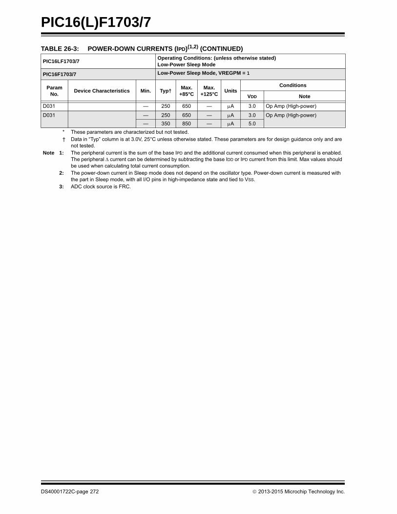
PIC16(L)F1703/7
D031 — 250 650 — A 3.0 Op Amp (High-power)
D031 — 250 650 — A 3.0 Op Amp (High-power)
— 350 850 — A 5.0
TABLE 26-3: POWER-DOWN CURRENTS (IPD)(1,2) (CONTINUED)
PIC16LF1703/7Operating Conditions: (unless otherwise stated)Low-Power Sleep Mode
PIC16F1703/7 Low-Power Sleep Mode, VREGPM = 1
ParamNo.
Device Characteristics Min. Typ†Max.
+85°CMax.
+125°CUnits
Conditions
VDD Note
* These parameters are characterized but not tested.† Data in “Typ” column is at 3.0V, 25°C unless otherwise stated. These parameters are for design guidance only and are
not tested.Note 1: The peripheral current is the sum of the base IPD and the additional current consumed when this peripheral is enabled.
The peripheral current can be determined by subtracting the base IDD or IPD current from this limit. Max values should be used when calculating total current consumption.
2: The power-down current in Sleep mode does not depend on the oscillator type. Power-down current is measured with the part in Sleep mode, with all I/O pins in high-impedance state and tied to VSS.
3: ADC clock source is FRC.
DS40001722C-page 272 2013-2015 Microchip Technology Inc.

PIC16(L)F1703/7
TABLE 26-4: I/O PORTSStandard Operating Conditions (unless otherwise stated)
ParamNo.
Sym. Characteristic Min. Typ† Max. Units Conditions
VIL Input Low Voltage
I/O PORT:
D034 with TTL buffer — — 0.8 V 4.5V VDD 5.5V
D034A — — 0.15 VDD V 1.8V VDD 4.5V
D035 with Schmitt Trigger buffer — — 0.2 VDD V 2.0V VDD 5.5V
with I2C levels — — 0.3 VDD V
with SMBus levels — — 0.8 V 2.7V VDD 5.5V
D036 MCLR — — 0.2 VDD V
VIH Input High Voltage
I/O ports:
D040 with TTL buffer 2.0 — — V 4.5V VDD 5.5V
D040A 0.25 VDD + 0.8
— — V 1.8V VDD 4.5V
D041 with Schmitt Trigger buffer 0.8 VDD — — V 2.0V VDD 5.5V
with I2C levels 0.7 VDD — — V
with SMBus levels 2.1 — — V 2.7V VDD 5.5V
D042 MCLR 0.8 VDD — — V
IIL Input Leakage Current(1)
D060 I/O Ports — ± 5 ± 125 nA VSS VPIN VDD, Pin at high-impedance, 85°C
— ± 5 ± 1000 nA VSS VPIN VDD, Pin at high-impedance, 125°C
D061 MCLR(2) — ± 50 ± 200 nA VSS VPIN VDD, Pin at high-impedance, 85°C
IPUR Weak Pull-up Current
D070* 25 100 200 A VDD = 3.0V, VPIN = VSS
VOL Output Low Voltage
D080 I/O ports— — 0.6 V
IOL = -8mA, VDD = 5VIOL = -6mA, VDD = 3.3VIOL = -1.8mA, VDD = 1.8V
VOH Output High Voltage
D090 I/O portsVDD - 0.7 — — V
IOH = 3.5mA, VDD = 5VIOH = 3mA, VDD = 3.3VIOH = 1mA, VDD = 1.8V
CIO Capacitive Loading Specs on Output Pins
D101A* All I/O pins — — 50 pF
* These parameters are characterized but not tested.† Data in “Typ” column is at 3.0V, 25°C unless otherwise stated. These parameters are for design guidance only and are
not tested.Note 1: Negative current is defined as current sourced by the pin.
2: The leakage current on the MCLR pin is strongly dependent on the applied voltage level. The specified levels represent normal operating conditions. Higher leakage current may be measured at different input voltages.
2013-2015 Microchip Technology Inc. DS40001722C-page 273
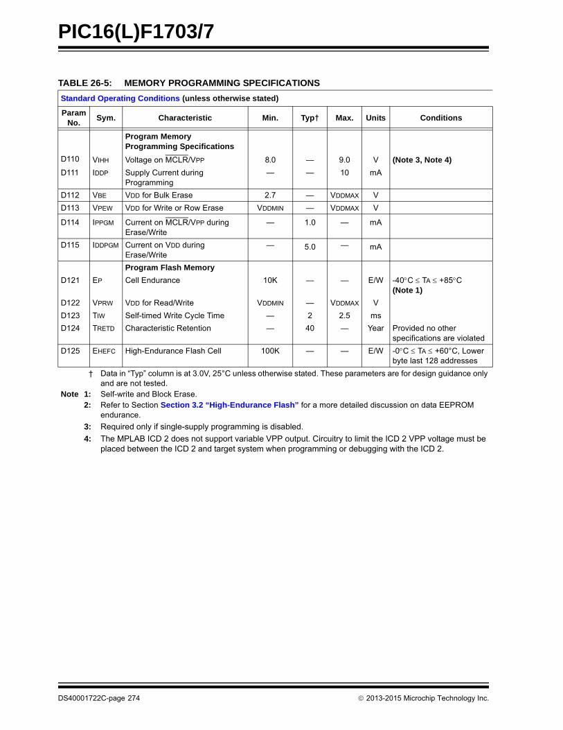
PIC16(L)F1703/7
TABLE 26-5: MEMORY PROGRAMMING SPECIFICATIONS
Standard Operating Conditions (unless otherwise stated)
ParamNo.
Sym. Characteristic Min. Typ† Max. Units Conditions
Program Memory Programming Specifications
D110 VIHH Voltage on MCLR/VPP 8.0 — 9.0 V (Note 3, Note 4)
D111 IDDP Supply Current during Programming
— — 10 mA
D112 VBE VDD for Bulk Erase 2.7 — VDDMAX V
D113 VPEW VDD for Write or Row Erase VDDMIN — VDDMAX V
D114 IPPGM Current on MCLR/VPP during Erase/Write
— 1.0 — mA
D115 IDDPGM Current on VDD during Erase/Write
— 5.0 — mA
Program Flash Memory
D121 EP Cell Endurance 10K — — E/W -40C TA +85C(Note 1)
D122 VPRW VDD for Read/Write VDDMIN — VDDMAX V
D123 TIW Self-timed Write Cycle Time — 2 2.5 ms
D124 TRETD Characteristic Retention — 40 — Year Provided no other specifications are violated
D125 EHEFC High-Endurance Flash Cell 100K — — E/W -0C TA +60°C, Lower byte last 128 addresses
† Data in “Typ” column is at 3.0V, 25°C unless otherwise stated. These parameters are for design guidance only and are not tested.
Note 1: Self-write and Block Erase.2: Refer to Section Section 3.2 “High-Endurance Flash” for a more detailed discussion on data EEPROM
endurance.
3: Required only if single-supply programming is disabled.
4: The MPLAB ICD 2 does not support variable VPP output. Circuitry to limit the ICD 2 VPP voltage must be placed between the ICD 2 and target system when programming or debugging with the ICD 2.
DS40001722C-page 274 2013-2015 Microchip Technology Inc.
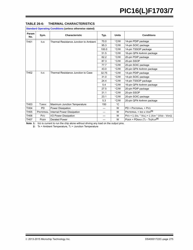
PIC16(L)F1703/7
TABLE 26-6: THERMAL CHARACTERISTICS
Standard Operating Conditions (unless otherwise stated)
ParamNo.
Sym. Characteristic Typ. Units Conditions
TH01 JA Thermal Resistance Junction to Ambient 70.0 C/W 14-pin PDIP package
95.3 C/W 14-pin SOIC package
100.0 C/W 14-pin TSSOP package
51.5 C/W 16-pin QFN 4x4mm package
62.2 C/W 20-pin PDIP package
87.3 C/W 20-pin SSOP
77.7 C/W 20-pin SOIC package
43.0 C/W 20-pin QFN 4x4mm package
TH02 JC Thermal Resistance Junction to Case 32.75 C/W 14-pin PDIP package
31.0 C/W 14-pin SOIC package
24.4 C/W 14-pin TSSOP package
5.4 C/W 16-pin QFN 4x4mm package
27.5 C/W 20-pin PDIP package
31.1 C/W 20-pin SSOP
23.1 C/W 20-pin SOIC package
5.3 C/W 20-pin QFN 4x4mm package
TH03 TJMAX Maximum Junction Temperature 150 CTH04 PD Power Dissipation — W PD = PINTERNAL + PI/O
TH05 PINTERNAL Internal Power Dissipation — W PINTERNAL = IDD x VDD(1)
TH06 PI/O I/O Power Dissipation — W PI/O = (IOL * VOL) + (IOH * (VDD - VOH))
TH07 PDER Derated Power — W PDER = PDMAX (TJ - TA)/JA(2)
Note 1: IDD is current to run the chip alone without driving any load on the output pins.2: TA = Ambient Temperature, TJ = Junction Temperature
2013-2015 Microchip Technology Inc. DS40001722C-page 275
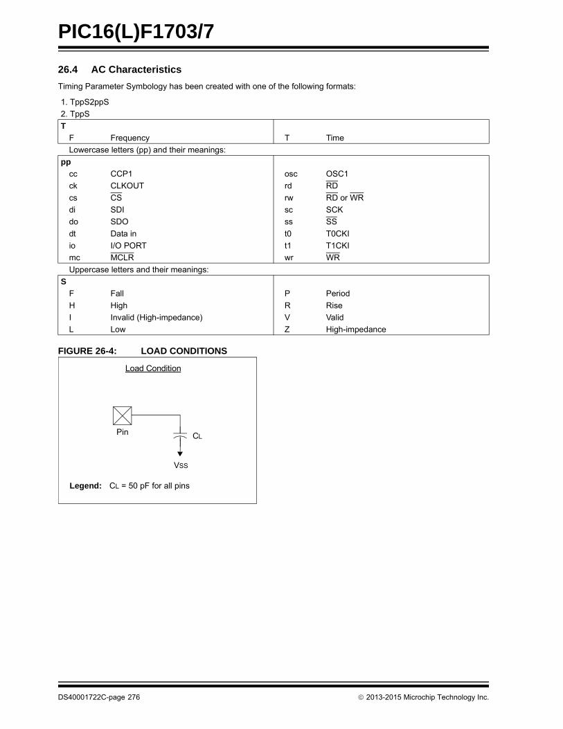
PIC16(L)F1703/7
26.4 AC Characteristics
Timing Parameter Symbology has been created with one of the following formats:
FIGURE 26-4: LOAD CONDITIONS
1. TppS2ppS
2. TppS
T
F Frequency T Time
Lowercase letters (pp) and their meanings:
pp
cc CCP1 osc OSC1
ck CLKOUT rd RD
cs CS rw RD or WR
di SDI sc SCK
do SDO ss SS
dt Data in t0 T0CKI
io I/O PORT t1 T1CKI
mc MCLR wr WR
Uppercase letters and their meanings:
S
F Fall P Period
H High R Rise
I Invalid (High-impedance) V Valid
L Low Z High-impedance
VSS
CL
Legend: CL = 50 pF for all pins
Load Condition
Pin
DS40001722C-page 276 2013-2015 Microchip Technology Inc.
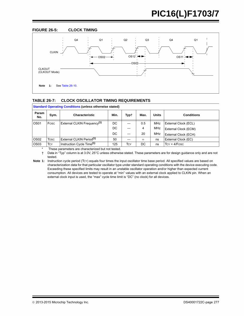
PIC16(L)F1703/7
FIGURE 26-5: CLOCK TIMING
TABLE 26-7: CLOCK OSCILLATOR TIMING REQUIREMENTS
Standard Operating Conditions (unless otherwise stated)
ParamNo.
Sym. Characteristic Min. Typ† Max. Units Conditions
OS01 FOSC External CLKIN Frequency(1) DC — 0.5 MHz External Clock (ECL)
DC — 4 MHz External Clock (ECM)
DC — 20 MHz External Clock (ECH)
OS02 TOSC External CLKIN Period(1) 50 — ns External Clock (EC)
OS03 TCY Instruction Cycle Time(1) 125 TCY DC ns TCY = 4/FOSC
* These parameters are characterized but not tested.† Data in “Typ” column is at 3.0V, 25°C unless otherwise stated. These parameters are for design guidance only and are not
tested.Note 1: Instruction cycle period (TCY) equals four times the input oscillator time base period. All specified values are based on
characterization data for that particular oscillator type under standard operating conditions with the device executing code. Exceeding these specified limits may result in an unstable oscillator operation and/or higher than expected current consumption. All devices are tested to operate at “min” values with an external clock applied to CLKIN pin. When an external clock input is used, the “max” cycle time limit is “DC” (no clock) for all devices.
CLKIN
CLKOUT
Q4 Q1 Q2 Q3 Q4 Q1
OS02
OS03
(CLKOUT Mode)
Note 1: See Table 26-10.
OS11OS12
2013-2015 Microchip Technology Inc. DS40001722C-page 277

PIC16(L)F1703/7
TABLE 26-8: OSCILLATOR PARAMETERS
FIGURE 26-6: HFINTOSC FREQUENCY ACCURACY OVER DEVICE VDD AND TEMPERATURE
Standard Operating Conditions (unless otherwise stated)
Param No.
Sym. CharacteristicFreq.
ToleranceMin. Typ† Max. Units Conditions
OS08 HFOSC Internal Calibrated HFINTOSC Frequency(1)
±2% — 16.0 — MHz
OS08A MFOSC Internal Calibrated MFINTOSC Frequency(1)
±2% — 500 — kHz
OS09 LFOSC Internal LFINTOSC Frequency — — 31 — kHz -40°C TA +125°C
OS10* TIOSC ST HFINTOSCWake-up from Sleep Start-up TimeMFINTOSCWake-up from Sleep Start-up Time
— — 3.2 8 s
— — 24 35 s
OS10A* TLFOSC ST LFINTOSC Wake-up from Sleep Start-up Time
— — 0.5 — ms -40°C TA +125°C
* These parameters are characterized but not tested.† Data in “Typ” column is at 3.0V, 25°C unless otherwise stated. These parameters are for design guidance only and are not tested.
Note 1: To ensure these oscillator frequency tolerances, VDD and VSS must be capacitively decoupled as close to the device as possible. 0.1 F and 0.01 F values in parallel are recommended.
2: See Figure 27-43: LFINTOSC Frequency, PIC16LF1703/7 Only., and Figure 27-44: LFINTOSC Frequency, PIC16F1703/7 Only..
125
25
2.0
0
60
85
VDD (V)
4.0 5.04.5
Tem
per
atu
re (
°C)
2.5 3.0 3.5 5.51.8-40
-20
± 5%
± 2%
± 5%
± 3%
DS40001722C-page 278 2013-2015 Microchip Technology Inc.

PIC16(L)F1703/7
TABLE 26-9: PLL CLOCK TIMING SPECIFICATIONS
Standard Operating Conditions (unless otherwise stated)
Param No.
Sym. Characteristic Min. Typ† Max. Units Conditions
F10 FOSC Oscillator Frequency Range 4 — 8 MHz
F11 FSYS On-Chip VCO System Frequency 16 — 32 MHz
F12 TRC PLL Start-up Time (Lock Time) — — 2 ms
F13* CLK CLKOUT Stability (Jitter) -0.25% — +0.25% %
* These parameters are characterized but not tested.
† Data in “Typ” column is at 5V, 25C unless otherwise stated. These parameters are for design guidance only and are not tested.
2013-2015 Microchip Technology Inc. DS40001722C-page 279
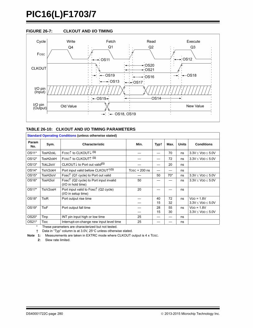
PIC16(L)F1703/7
FIGURE 26-7: CLKOUT AND I/O TIMING
TABLE 26-10: CLKOUT AND I/O TIMING PARAMETERS
Standard Operating Conditions (unless otherwise stated)
Param No.
Sym. Characteristic Min. Typ† Max. Units Conditions
OS11* TosH2ckL FOSC to CLKOUT (1) — — 70 ns 3.3V VDD 5.0V
OS12* TosH2ckH FOSC to CLKOUT (1) — — 72 ns 3.3V VDD 5.0V
OS13* TckL2ioV CLKOUT to Port out valid(1) — — 20 ns
OS14* TioV2ckH Port input valid before CLKOUT(1) TOSC + 200 ns — — ns
OS15* TosH2ioV Fosc (Q1 cycle) to Port out valid — 50 70* ns 3.3V VDD 5.0V
OS16* TosH2ioI Fosc (Q2 cycle) to Port input invalid (I/O in hold time)
50 — — ns 3.3V VDD 5.0V
OS17* TioV2osH Port input valid to Fosc(Q2 cycle)(I/O in setup time)
20 — — ns
OS18* TioR Port output rise time ——
4015
7232
ns VDD = 1.8V3.3V VDD 5.0V
OS19* TioF Port output fall time ——
2815
5530
ns VDD = 1.8V3.3V VDD 5.0V
OS20* Tinp INT pin input high or low time 25 — — ns
OS21* Tioc Interrupt-on-change new input level time 25 — — ns
* These parameters are characterized but not tested.† Data in “Typ” column is at 3.0V, 25C unless otherwise stated.
Note 1: Measurements are taken in EXTRC mode where CLKOUT output is 4 x TOSC.2: Slew rate limited.
FOSC
CLKOUT
I/O pin(Input)
I/O pin(Output)
Q4 Q1 Q2 Q3
OS11
OS19
OS13
OS15
OS18, OS19
OS20OS21
OS17
OS16
OS14
OS12
OS18
Old Value New Value
Write Fetch Read ExecuteCycle
DS40001722C-page 280 2013-2015 Microchip Technology Inc.
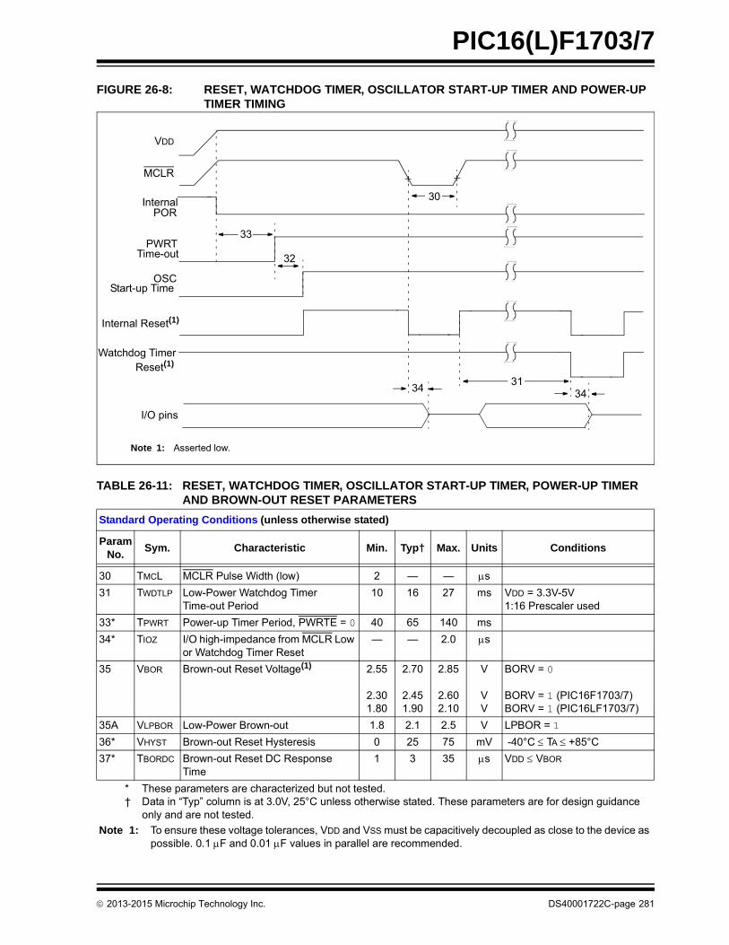
PIC16(L)F1703/7
FIGURE 26-8: RESET, WATCHDOG TIMER, OSCILLATOR START-UP TIMER AND POWER-UP TIMER TIMING
TABLE 26-11: RESET, WATCHDOG TIMER, OSCILLATOR START-UP TIMER, POWER-UP TIMER AND BROWN-OUT RESET PARAMETERS
Standard Operating Conditions (unless otherwise stated)
Param No.
Sym. Characteristic Min. Typ† Max. Units Conditions
30 TMCL MCLR Pulse Width (low) 2 — — s
31 TWDTLP Low-Power Watchdog Timer Time-out Period
10 16 27 ms VDD = 3.3V-5V1:16 Prescaler used
33* TPWRT Power-up Timer Period, PWRTE = 0 40 65 140 ms
34* TIOZ I/O high-impedance from MCLR Low or Watchdog Timer Reset
— — 2.0 s
35 VBOR Brown-out Reset Voltage(1) 2.55
2.301.80
2.70
2.451.90
2.85
2.602.10
V
VV
BORV = 0
BORV = 1 (PIC16F1703/7)BORV = 1 (PIC16LF1703/7)
35A VLPBOR Low-Power Brown-out 1.8 2.1 2.5 V LPBOR = 1
36* VHYST Brown-out Reset Hysteresis 0 25 75 mV -40°C TA +85°C
37* TBORDC Brown-out Reset DC Response Time
1 3 35 s VDD VBOR
* These parameters are characterized but not tested.† Data in “Typ” column is at 3.0V, 25°C unless otherwise stated. These parameters are for design guidance
only and are not tested.
Note 1: To ensure these voltage tolerances, VDD and VSS must be capacitively decoupled as close to the device as possible. 0.1 F and 0.01 F values in parallel are recommended.
VDD
MCLR
InternalPOR
PWRTTime-out
OSCStart-up Time
Internal Reset(1)
Watchdog Timer
33
32
30
3134
I/O pins
34
Note 1: Asserted low.
Reset(1)
2013-2015 Microchip Technology Inc. DS40001722C-page 281
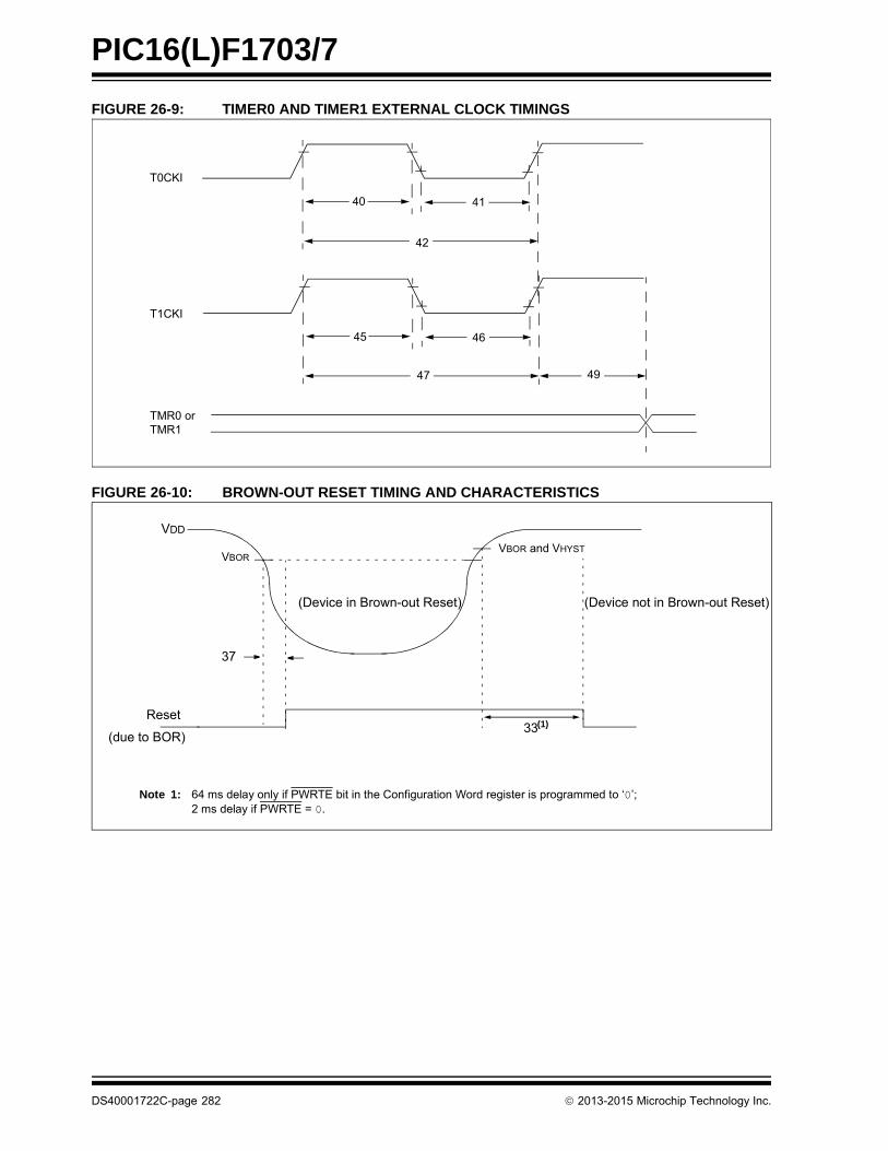
PIC16(L)F1703/7
FIGURE 26-9: TIMER0 AND TIMER1 EXTERNAL CLOCK TIMINGS
FIGURE 26-10: BROWN-OUT RESET TIMING AND CHARACTERISTICS
T0CKI
T1CKI
40 41
42
45 46
47 49
TMR0 orTMR1
VBOR
VDD
(Device in Brown-out Reset) (Device not in Brown-out Reset)
33(1)
Note 1: 64 ms delay only if PWRTE bit in the Configuration Word register is programmed to ‘0’; 2 ms delay if PWRTE = 0.
Reset
(due to BOR)
VBOR and VHYST
37
DS40001722C-page 282 2013-2015 Microchip Technology Inc.
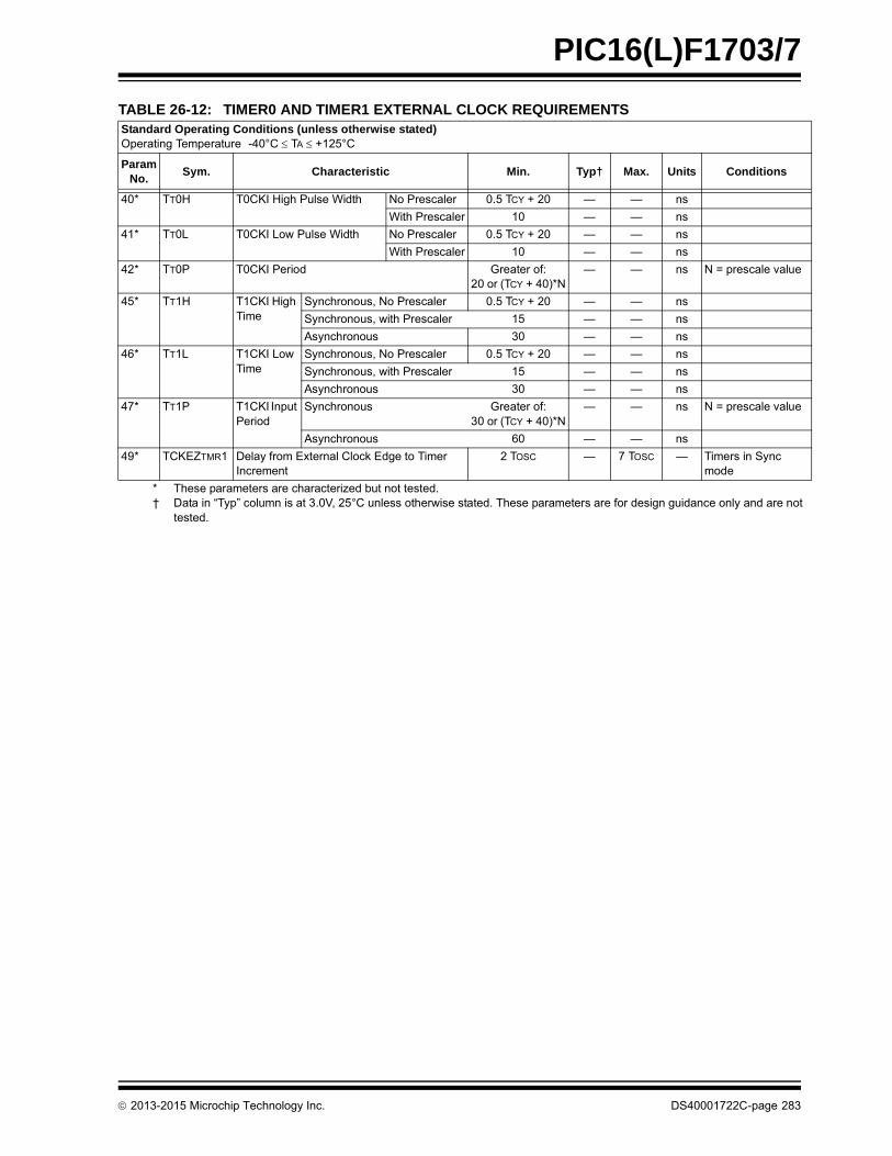
PIC16(L)F1703/7
TABLE 26-12: TIMER0 AND TIMER1 EXTERNAL CLOCK REQUIREMENTSStandard Operating Conditions (unless otherwise stated)Operating Temperature -40°C TA +125°C
Param No.
Sym. Characteristic Min. Typ† Max. Units Conditions
40* TT0H T0CKI High Pulse Width No Prescaler 0.5 TCY + 20 — — ns
With Prescaler 10 — — ns
41* TT0L T0CKI Low Pulse Width No Prescaler 0.5 TCY + 20 — — ns
With Prescaler 10 — — ns
42* TT0P T0CKI Period Greater of:20 or (TCY + 40)*N
— — ns N = prescale value
45* TT1H T1CKI High Time
Synchronous, No Prescaler 0.5 TCY + 20 — — ns
Synchronous, with Prescaler 15 — — ns
Asynchronous 30 — — ns
46* TT1L T1CKI Low Time
Synchronous, No Prescaler 0.5 TCY + 20 — — ns
Synchronous, with Prescaler 15 — — ns
Asynchronous 30 — — ns
47* TT1P T1CKI Input Period
Synchronous Greater of:30 or (TCY + 40)*N
— — ns N = prescale value
Asynchronous 60 — — ns
49* TCKEZTMR1 Delay from External Clock Edge to Timer Increment
2 TOSC — 7 TOSC — Timers in Sync mode
* These parameters are characterized but not tested.† Data in “Typ” column is at 3.0V, 25°C unless otherwise stated. These parameters are for design guidance only and are not
tested.
2013-2015 Microchip Technology Inc. DS40001722C-page 283
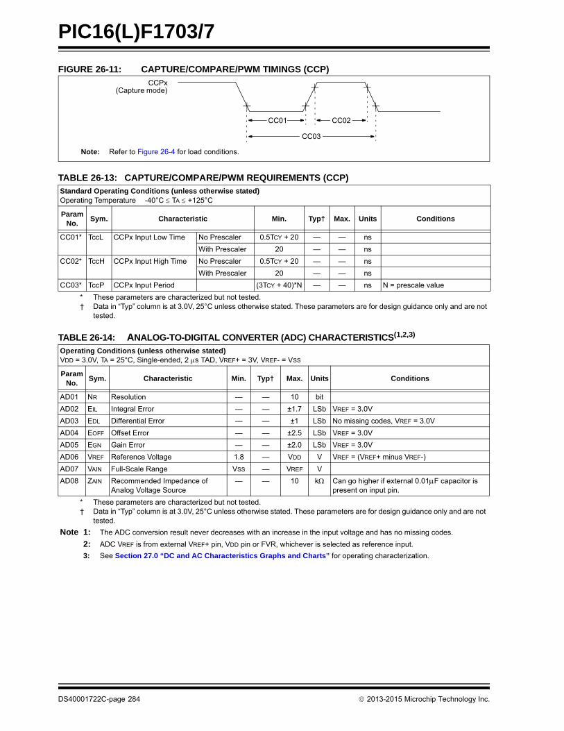
PIC16(L)F1703/7
FIGURE 26-11: CAPTURE/COMPARE/PWM TIMINGS (CCP)
TABLE 26-13: CAPTURE/COMPARE/PWM REQUIREMENTS (CCP)
TABLE 26-14: ANALOG-TO-DIGITAL CONVERTER (ADC) CHARACTERISTICS(1,2,3)
Standard Operating Conditions (unless otherwise stated)Operating Temperature -40°C TA +125°C
Param No.
Sym. Characteristic Min. Typ† Max. Units Conditions
CC01* TccL CCPx Input Low Time No Prescaler 0.5TCY + 20 — — ns
With Prescaler 20 — — ns
CC02* TccH CCPx Input High Time No Prescaler 0.5TCY + 20 — — ns
With Prescaler 20 — — ns
CC03* TccP CCPx Input Period (3TCY + 40)*N — — ns N = prescale value
* These parameters are characterized but not tested.† Data in “Typ” column is at 3.0V, 25°C unless otherwise stated. These parameters are for design guidance only and are not
tested.
Operating Conditions (unless otherwise stated)VDD = 3.0V, TA = 25°C, Single-ended, 2 s TAD, VREF+ = 3V, VREF- = VSS
Param No.
Sym. Characteristic Min. Typ† Max. Units Conditions
AD01 NR Resolution — — 10 bit
AD02 EIL Integral Error — — ±1.7 LSb VREF = 3.0V
AD03 EDL Differential Error — — ±1 LSb No missing codes, VREF = 3.0V
AD04 EOFF Offset Error — — ±2.5 LSb VREF = 3.0V
AD05 EGN Gain Error — — ±2.0 LSb VREF = 3.0V
AD06 VREF Reference Voltage 1.8 — VDD V VREF = (VREF+ minus VREF-)
AD07 VAIN Full-Scale Range VSS — VREF V
AD08 ZAIN Recommended Impedance of Analog Voltage Source
— — 10 k Can go higher if external 0.01F capacitor is present on input pin.
* These parameters are characterized but not tested.† Data in “Typ” column is at 3.0V, 25°C unless otherwise stated. These parameters are for design guidance only and are not
tested.
Note 1: The ADC conversion result never decreases with an increase in the input voltage and has no missing codes.
2: ADC VREF is from external VREF+ pin, VDD pin or FVR, whichever is selected as reference input.
3: See Section 27.0 “DC and AC Characteristics Graphs and Charts” for operating characterization.
Note: Refer to Figure 26-4 for load conditions.
(Capture mode)
CC01 CC02
CC03
CCPx
DS40001722C-page 284 2013-2015 Microchip Technology Inc.

PIC16(L)F1703/7
TABLE 26-15: ADC CONVERSION REQUIREMENTS
Standard Operating Conditions (unless otherwise stated)
ParamNo.
Sym. Characteristic Min. Typ† Max. Units Conditions
AD130* TAD ADC Clock Period (TADC) 1.0 — 9.0 s FOSC-based
ADC Internal FRC Oscillator Period (TFRC)
1.0 2 6.0 s ADCS<1:0> = 11 (ADC FRC mode)
AD131 TCNV Conversion Time (not including Acquisition Time)(1)
— 11 — TAD Set GO/DONE bit to conversioncomplete
AD132* TACQ Acquisition Time — 5.0 — s
AD133* THCD Holding Capacitor Disconnect Time — 1/2 TAD — ADCS<2:0> x11 (FOSC based)
— 1/2 TAD + 1TCY — ADCS<2:0> = x11 (FRC based)
* These parameters are characterized but not tested.† Data in “Typ” column is at 3.0V, 25°C unless otherwise stated. These parameters are for design guidance only and are not
tested.Note 1: The ADRES register may be read on the following TCY cycle.
2013-2015 Microchip Technology Inc. DS40001722C-page 285
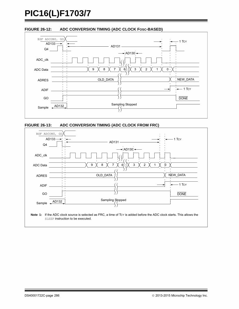
PIC16(L)F1703/7
FIGURE 26-12: ADC CONVERSION TIMING (ADC CLOCK FOSC-BASED)
FIGURE 26-13: ADC CONVERSION TIMING (ADC CLOCK FROM FRC)
AD131
AD130
BSF ADCON0, GO
Q4
ADC_clk
ADC Data
ADRES
ADIF
GO
Sample
OLD_DATA
Sampling Stopped
DONE
NEW_DATA
9 8 7 3 2 1 0
1 TCY
6
AD133
1 TCY
AD132
AD132
AD131
AD130
BSF ADCON0, GO
Q4
ADC_clk
ADC Data
ADRES
ADIF
GO
Sample
OLD_DATA
Sampling Stopped
DONE
NEW_DATA
9 7 3 2 1 0
Note 1: If the ADC clock source is selected as FRC, a time of TCY is added before the ADC clock starts. This allows the SLEEP instruction to be executed.
AD133
68
1 TCY
1 TCY
DS40001722C-page 286 2013-2015 Microchip Technology Inc.

PIC16(L)F1703/7
TABLE 26-16: OPERATIONAL AMPLIFIER (OPA)
TABLE 26-17: ZERO CROSS PIN SPECIFICATIONS
Operating Conditions (unless otherwise stated)VDD = 3.0V, TA = 25°C, OPAxSP = 1 (High GBWP mode)
ParamNo.
Symbol Parameters Min. Typ. Max. Units Conditions
OPA01* GBWP Gain Bandwidth Product — 3.5 — MHz
OPA02* TON Turn-on Time — 10 — s
OPA03* PM Phase Margin — 40 — degrees
OPA04* SR Slew Rate — 3 — V/s
OPA05 OFF Offset — ±3 ±9 mV
OPA06 CMRR Common-Mode Rejection Ratio 52 70 — dB
OPA07* AOL Open Loop Gain — 90 — dB
OPA08 VICM Input Common-Mode Voltage 0 — VDD V VDD > 2.5V
OPA09* PSRR Power Supply Rejection Ratio — 80 — dB
* These parameters are characterized but not tested.
Operating Conditions (unless otherwise stated)VDD = 3.0V, TA = 25°C
Param.No.
Sym. Characteristics Min. Typ. Max. Units Comments
ZC01 ZCPINV Voltage on Zero Cross Pin — 0.75 — V
ZC02 ZCSRC Source current — — -600 A
ZC03 ZCSNK Sink current 600 — — A
ZC04 ZCISW Response Time Rising Edge — 1 — s
Response Time Falling Edge — 1 — s
ZC05 ZCOUT Response Time Rising Edge — 1 — s
Response Time Falling Edge — 1 — s
* These parameters are characterized but not tested.
2013-2015 Microchip Technology Inc. DS40001722C-page 287
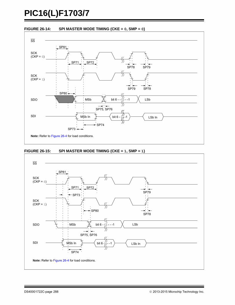
PIC16(L)F1703/7
FIGURE 26-14: SPI MASTER MODE TIMING (CKE = 0, SMP = 0)
FIGURE 26-15: SPI MASTER MODE TIMING (CKE = 1, SMP = 1)
SS
SCK(CKP = 0)
SCK(CKP = 1)
SDO
SDI
SP81
SP71 SP72
SP73SP74
SP75, SP76
SP78SP79
SP80
SP79SP78
MSb LSbbit 6 - - - - - -1
MSb In LSb Inbit 6 - - - -1
Note: Refer to Figure 26-4 for load conditions.
SS
SCK(CKP = 0)
SCK(CKP = 1)
SDO
SDI
SP81
SP71 SP72
SP74
SP75, SP76
SP78SP80
MSb
SP79SP73
MSb In
bit 6 - - - - - -1
LSb Inbit 6 - - - -1
LSb
Note: Refer to Figure 26-4 for load conditions.
DS40001722C-page 288 2013-2015 Microchip Technology Inc.
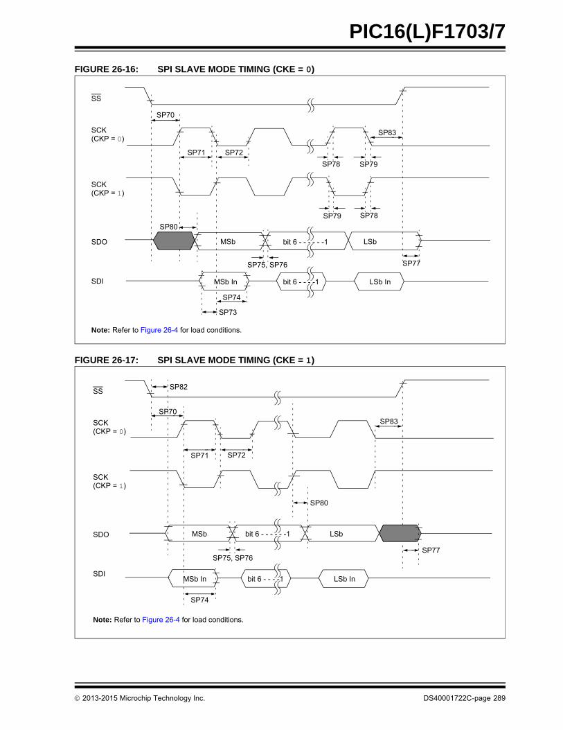
PIC16(L)F1703/7
FIGURE 26-16: SPI SLAVE MODE TIMING (CKE = 0)
FIGURE 26-17: SPI SLAVE MODE TIMING (CKE = 1)
SS
SCK(CKP = 0)
SCK(CKP = 1)
SDO
SDI
SP70
SP71 SP72
SP73
SP74
SP75, SP76 SP77
SP78SP79
SP80
SP79SP78
MSb LSbbit 6 - - - - - -1
MSb In bit 6 - - - -1 LSb In
SP83
Note: Refer to Figure 26-4 for load conditions.
SS
SCK(CKP = 0)
SCK(CKP = 1)
SDO
SDI
SP70
SP71 SP72
SP82
SP74
SP75, SP76
MSb bit 6 - - - - - -1 LSb
SP77
MSb In bit 6 - - - -1 LSb In
SP80
SP83
Note: Refer to Figure 26-4 for load conditions.
2013-2015 Microchip Technology Inc. DS40001722C-page 289
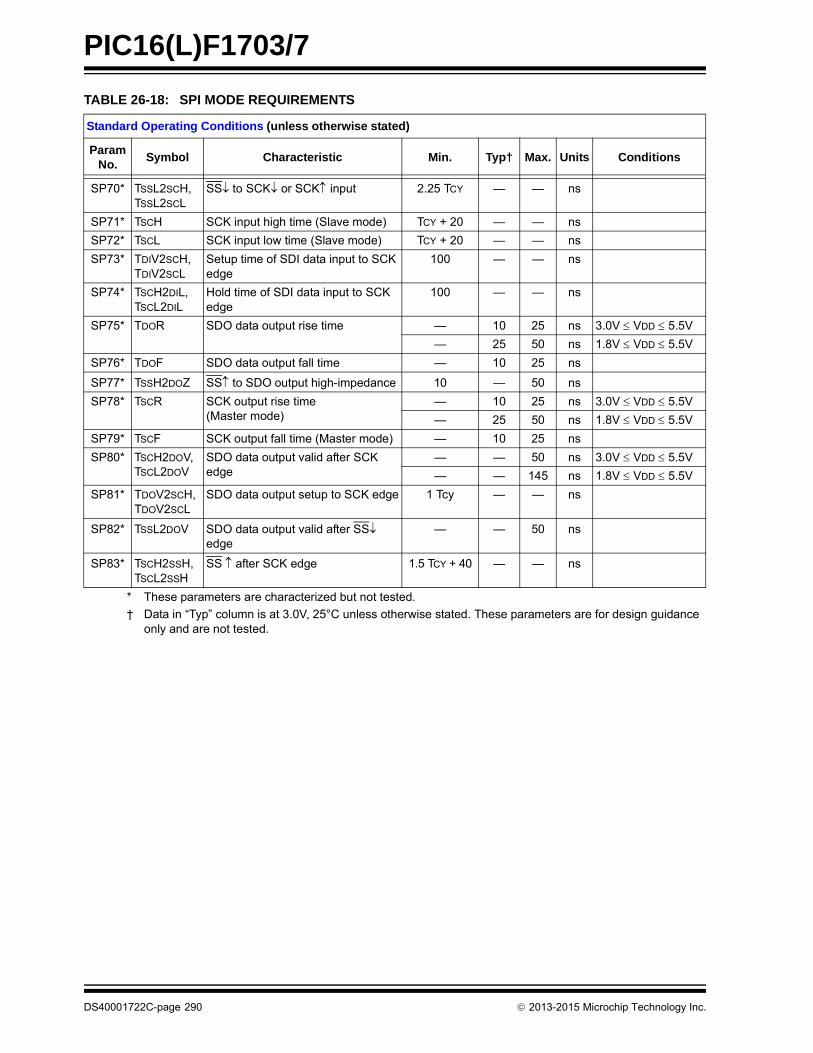
PIC16(L)F1703/7
TABLE 26-18: SPI MODE REQUIREMENTS
Standard Operating Conditions (unless otherwise stated)
Param No.
Symbol Characteristic Min. Typ† Max. Units Conditions
SP70* TSSL2SCH, TSSL2SCL
SS to SCK or SCK input 2.25 TCY — — ns
SP71* TSCH SCK input high time (Slave mode) TCY + 20 — — ns
SP72* TSCL SCK input low time (Slave mode) TCY + 20 — — ns
SP73* TDIV2SCH, TDIV2SCL
Setup time of SDI data input to SCK edge
100 — — ns
SP74* TSCH2DIL, TSCL2DIL
Hold time of SDI data input to SCK edge
100 — — ns
SP75* TDOR SDO data output rise time — 10 25 ns 3.0V VDD 5.5V
— 25 50 ns 1.8V VDD 5.5V
SP76* TDOF SDO data output fall time — 10 25 ns
SP77* TSSH2DOZ SS to SDO output high-impedance 10 — 50 ns
SP78* TSCR SCK output rise time (Master mode)
— 10 25 ns 3.0V VDD 5.5V
— 25 50 ns 1.8V VDD 5.5V
SP79* TSCF SCK output fall time (Master mode) — 10 25 ns
SP80* TSCH2DOV,TSCL2DOV
SDO data output valid after SCK edge
— — 50 ns 3.0V VDD 5.5V
— — 145 ns 1.8V VDD 5.5V
SP81* TDOV2SCH,TDOV2SCL
SDO data output setup to SCK edge 1 Tcy — — ns
SP82* TSSL2DOV SDO data output valid after SS edge
— — 50 ns
SP83* TSCH2SSH,TSCL2SSH
SS after SCK edge 1.5 TCY + 40 — — ns
* These parameters are characterized but not tested.
† Data in “Typ” column is at 3.0V, 25°C unless otherwise stated. These parameters are for design guidance only and are not tested.
DS40001722C-page 290 2013-2015 Microchip Technology Inc.
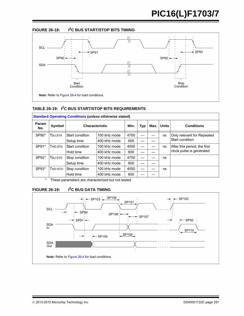
PIC16(L)F1703/7
FIGURE 26-18: I2C BUS START/STOP BITS TIMING
TABLE 26-19: I2C BUS START/STOP BITS REQUIREMENTS
FIGURE 26-19: I2C BUS DATA TIMING
Standard Operating Conditions (unless otherwise stated)
ParamNo.
Symbol Characteristic Min. Typ Max. Units Conditions
SP90* TSU:STA Start condition 100 kHz mode 4700 — — ns Only relevant for Repeated Start conditionSetup time 400 kHz mode 600 — —
SP91* THD:STA Start condition 100 kHz mode 4000 — — ns After this period, the first clock pulse is generatedHold time 400 kHz mode 600 — —
SP92* TSU:STO Stop condition 100 kHz mode 4700 — — ns
Setup time 400 kHz mode 600 — —
SP93* THD:STO Stop condition 100 kHz mode 4000 — — ns
Hold time 400 kHz mode 600 — —
* These parameters are characterized but not tested.
Note: Refer to Figure 26-4 for load conditions.
SP91
SP92
SP93SCL
SDA
StartCondition
StopCondition
SP90
Note: Refer to Figure 26-4 for load conditions.
SP90
SP91 SP92
SP100
SP101SP103
SP106SP107
SP109SP109
SP110
SP102
SCL
SDAIn
SDAOut
2013-2015 Microchip Technology Inc. DS40001722C-page 291
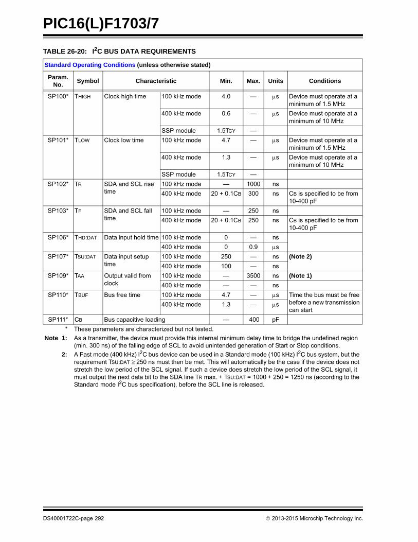
PIC16(L)F1703/7
TABLE 26-20: I2C BUS DATA REQUIREMENTS
Standard Operating Conditions (unless otherwise stated)
Param.No.
Symbol Characteristic Min. Max. Units Conditions
SP100* THIGH Clock high time 100 kHz mode 4.0 — s Device must operate at a minimum of 1.5 MHz
400 kHz mode 0.6 — s Device must operate at a minimum of 10 MHz
SSP module 1.5TCY —
SP101* TLOW Clock low time 100 kHz mode 4.7 — s Device must operate at a minimum of 1.5 MHz
400 kHz mode 1.3 — s Device must operate at a minimum of 10 MHz
SSP module 1.5TCY —
SP102* TR SDA and SCL rise time
100 kHz mode — 1000 ns
400 kHz mode 20 + 0.1CB 300 ns CB is specified to be from 10-400 pF
SP103* TF SDA and SCL fall time
100 kHz mode — 250 ns
400 kHz mode 20 + 0.1CB 250 ns CB is specified to be from 10-400 pF
SP106* THD:DAT Data input hold time 100 kHz mode 0 — ns
400 kHz mode 0 0.9 s
SP107* TSU:DAT Data input setup time
100 kHz mode 250 — ns (Note 2)
400 kHz mode 100 — ns
SP109* TAA Output valid from clock
100 kHz mode — 3500 ns (Note 1)
400 kHz mode — — ns
SP110* TBUF Bus free time 100 kHz mode 4.7 — s Time the bus must be free before a new transmission can start
400 kHz mode 1.3 — s
SP111* CB Bus capacitive loading — 400 pF
* These parameters are characterized but not tested.
Note 1: As a transmitter, the device must provide this internal minimum delay time to bridge the undefined region (min. 300 ns) of the falling edge of SCL to avoid unintended generation of Start or Stop conditions.
2: A Fast mode (400 kHz) I2C bus device can be used in a Standard mode (100 kHz) I2C bus system, but the requirement TSU:DAT 250 ns must then be met. This will automatically be the case if the device does not stretch the low period of the SCL signal. If such a device does stretch the low period of the SCL signal, it must output the next data bit to the SDA line TR max. + TSU:DAT = 1000 + 250 = 1250 ns (according to the Standard mode I2C bus specification), before the SCL line is released.
DS40001722C-page 292 2013-2015 Microchip Technology Inc.
PIC16(L)F1703/7
27.0 DC AND AC CHARACTERISTICS GRAPHS AND CHARTS
The graphs and tables provided in this section are for design guidance and are not tested.
In some graphs or tables, the data presented are outside specified operating range (i.e., outside specified VDD
range). This is for information only and devices are ensured to operate properly only within the specified range.
Unless otherwise noted, all graphs apply to both the L and LF devices.
“Typical” represents the mean of the distribution at 25C. “MAXIMUM”, “Max.”, “MINIMUM” or “Min.”represents (mean + 3) or (mean - 3) respectively, where is a standard deviation, over eachtemperature range.
Note: The graphs and tables provided following this note are a statistical summary based on a limited number ofsamples and are provided for informational purposes only. The performance characteristics listed hereinare not tested or guaranteed. In some graphs or tables, the data presented may be outside the specifiedoperating range (e.g., outside specified power supply range) and therefore, outside the warranted range.
2013-2015 Microchip Technology Inc. DS40001722C-page 293
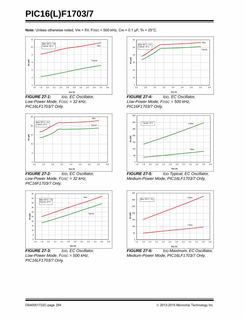
PIC16(L)F1703/7
Note: Unless otherwise noted, VIN = 5V, FOSC = 500 kHz, CIN = 0.1 µF, TA = 25°C.
FIGURE 27-1: IDD, EC Oscillator, Low-Power Mode, FOSC = 32 kHz, PIC16LF1703/7 Only.
FIGURE 27-2: IDD, EC Oscillator, Low-Power Mode, FOSC = 32 kHz, PIC16F1703/7 Only.
FIGURE 27-3: IDD, EC Oscillator, Low-Power Mode, FOSC = 500 kHz, PIC16LF1703/7 Only.
FIGURE 27-4: IDD, EC Oscillator, Low-Power Mode, FOSC = 500 kHz, PIC16F1703/7 Only.
FIGURE 27-5: IDD Typical, EC Oscillator, Medium-Power Mode, PIC16LF1703/7 Only.
FIGURE 27-6: IDD Maximum, EC Oscillator, Medium-Power Mode, PIC16LF1703/7 Only.
, , ,
Typical
Max.
0
2
4
6
8
10
12
1.6 1.8 2.0 2.2 2.4 2.6 2.8 3.0 3.2 3.4 3.6 3.8
IDD
(μA
)
VDD (V)
Max: 85°C + 3Typical: 25°C
Typical
Max.
0
5
10
15
20
25
2.0 2.5 3.0 3.5 4.0 4.5 5.0 5.5 6.0
IDD
(μA
)
VDD (V)
Max: 85°C + 3Typical: 25°C
, , ,
Max.
Typical
0
5
10
15
20
25
30
35
40
45
50
1.6 1.8 2.0 2.2 2.4 2.6 2.8 3.0 3.2 3.4 3.6 3.8
IDD
(μA
)
VDD (V)
Max: 85°C + 3Typical: 25°C
Typical
Max.
0
10
20
30
40
50
60
2.0 2.5 3.0 3.5 4.0 4.5 5.0 5.5 6.0
IDD
(μA
)
VDD (V)
Max: 85°C + 3Typical: 25°C
4 MHz
1 MHz
0
50
100
150
200
250
300
350
1.6 1.8 2.0 2.2 2.4 2.6 2.8 3.0 3.2 3.4 3.6 3.8
IDD
(μA
)
VDD (V)
Typical: 25°C
, ,
4 MHz
1 MHz
0
50
100
150
200
250
300
350
1.6 1.8 2.0 2.2 2.4 2.6 2.8 3.0 3.2 3.4 3.6 3.8
IDD
(μA
)
VDD (V)
Max: 85°C + 3
DS40001722C-page 294 2013-2015 Microchip Technology Inc.
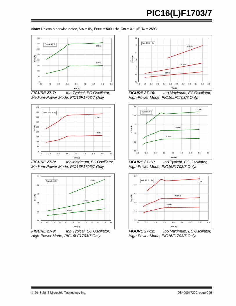
PIC16(L)F1703/7
Note: Unless otherwise noted, VIN = 5V, FOSC = 500 kHz, CIN = 0.1 µF, TA = 25°C.
FIGURE 27-7: IDD Typical, EC Oscillator, Medium-Power Mode, PIC16F1703/7 Only.
FIGURE 27-8: IDD Maximum, EC Oscillator, Medium-Power Mode, PIC16F1703/7 Only.
FIGURE 27-9: IDD Typical, EC Oscillator, High-Power Mode, PIC16LF1703/7 Only.
FIGURE 27-10: IDD Maximum, EC Oscillator, High-Power Mode, PIC16LF1703/7 Only.
FIGURE 27-11: IDD Typical, EC Oscillator, High-Power Mode, PIC16F1703/7 Only.
FIGURE 27-12: IDD Maximum, EC Oscillator, High-Power Mode, PIC16F1703/7 Only.
4 MHz
1 MHz
0
50
100
150
200
250
300
350
400
2.0 2.5 3.0 3.5 4.0 4.5 5.0 5.5 6.0
IDD
(μA
)
VDD (V)
Typical: 25°C
, ,
4 MHz
1 MHz
0
50
100
150
200
250
300
350
400
450
2.0 2.5 3.0 3.5 4.0 4.5 5.0 5.5 6.0
IDD
(μA
)
VDD (V)
Max: 85°C + 3
32 MHz
16 MHz
8 MHz
0.0
0.5
1.0
1.5
2.0
2.5
1.6 1.8 2.0 2.2 2.4 2.6 2.8 3.0 3.2 3.4 3.6 3.8
IDD
(mA
)
VDD (V)
Typical: 25°C
32 MHz
16 MHz
8 MHz
0.0
0.5
1.0
1.5
2.0
2.5
3.0
1.6 1.8 2.0 2.2 2.4 2.6 2.8 3.0 3.2 3.4 3.6 3.8
IDD
(mA
)
VDD (V)
Max: 85°C + 3
32 MHz
16 MHz
8 MHz
0.0
0.5
1.0
1.5
2.0
2.5
2.0 2.5 3.0 3.5 4.0 4.5 5.0 5.5 6.0
IDD
(mA
)
VDD (V)
Typical: 25°C
32 MHz
16 MHz
8 MHz
0.0
0.5
1.0
1.5
2.0
2.5
2.0 2.5 3.0 3.5 4.0 4.5 5.0 5.5 6.0
IDD
(mA
)
VDD (V)
Max: 85°C + 3
2013-2015 Microchip Technology Inc. DS40001722C-page 295
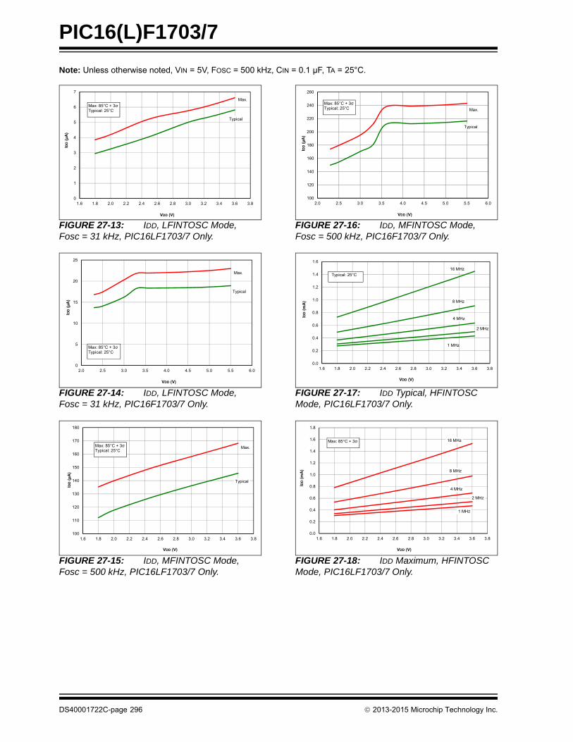
PIC16(L)F1703/7
Note: Unless otherwise noted, VIN = 5V, FOSC = 500 kHz, CIN = 0.1 µF, TA = 25°C.
FIGURE 27-13: IDD, LFINTOSC Mode, Fosc = 31 kHz, PIC16LF1703/7 Only.
FIGURE 27-14: IDD, LFINTOSC Mode, Fosc = 31 kHz, PIC16F1703/7 Only.
FIGURE 27-15: IDD, MFINTOSC Mode, Fosc = 500 kHz, PIC16LF1703/7 Only.
FIGURE 27-16: IDD, MFINTOSC Mode, Fosc = 500 kHz, PIC16F1703/7 Only.
FIGURE 27-17: IDD Typical, HFINTOSC Mode, PIC16LF1703/7 Only.
FIGURE 27-18: IDD Maximum, HFINTOSC Mode, PIC16LF1703/7 Only.
Typical
Max.
0
1
2
3
4
5
6
7
1.6 1.8 2.0 2.2 2.4 2.6 2.8 3.0 3.2 3.4 3.6 3.8
IDD
(μA
)
VDD (V)
Max: 85°C + 3Typical: 25°C
Typical
Max.
0
5
10
15
20
25
2.0 2.5 3.0 3.5 4.0 4.5 5.0 5.5 6.0
IDD
(μA
)
VDD (V)
Max: 85°C + 3Typical: 25°C
Typical
Max.
100
110
120
130
140
150
160
170
180
1.6 1.8 2.0 2.2 2.4 2.6 2.8 3.0 3.2 3.4 3.6 3.8
IDD
(μA
)
VDD (V)
Max: 85°C + 3Typical: 25°C
Typical
Max.
100
120
140
160
180
200
220
240
260
2.0 2.5 3.0 3.5 4.0 4.5 5.0 5.5 6.0
IDD
(μA
)
VDD (V)
Max: 85°C + 3Typical: 25°C
16 MHz
8 MHz
4 MHz
2 MHz
1 MHz
0.0
0.2
0.4
0.6
0.8
1.0
1.2
1.4
1.6
1.6 1.8 2.0 2.2 2.4 2.6 2.8 3.0 3.2 3.4 3.6 3.8
IDD
(mA
)
VDD (V)
Typical: 25°C
16 MHz
8 MHz
4 MHz
2 MHz
1 MHz
0.0
0.2
0.4
0.6
0.8
1.0
1.2
1.4
1.6
1.8
1.6 1.8 2.0 2.2 2.4 2.6 2.8 3.0 3.2 3.4 3.6 3.8
IDD
(mA
)
VDD (V)
Max: 85°C + 3
DS40001722C-page 296 2013-2015 Microchip Technology Inc.
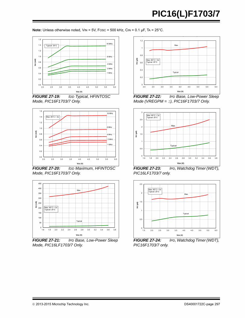
PIC16(L)F1703/7
Note: Unless otherwise noted, VIN = 5V, FOSC = 500 kHz, CIN = 0.1 µF, TA = 25°C.
FIGURE 27-19: IDD Typical, HFINTOSC Mode, PIC16F1703/7 Only.
FIGURE 27-20: IDD Maximum, HFINTOSC Mode, PIC16F1703/7 Only.
FIGURE 27-21: IPD Base, Low-Power Sleep Mode, PIC16LF1703/7 Only.
FIGURE 27-22: IPD Base, Low-Power Sleep Mode (VREGPM = 1), PIC16F1703/7 Only.
FIGURE 27-23: IPD, Watchdog Timer (WDT), PIC16LF1703/7 only.
FIGURE 27-24: IPD, Watchdog Timer (WDT), PIC16F1703/7 only.
16 MHz
8 MHz
4 MHz
2 MHz
1 MHz
0.0
0.2
0.4
0.6
0.8
1.0
1.2
1.4
1.6
2.0 2.5 3.0 3.5 4.0 4.5 5.0 5.5 6.0
IDD
(mA
)
VDD (V)
Typical: 25°C
16 MHz
8 MHz
4 MHz
2 MHz
1 MHz
0.0
0.2
0.4
0.6
0.8
1.0
1.2
1.4
1.6
2.0 2.5 3.0 3.5 4.0 4.5 5.0 5.5 6.0
IDD
(mA
)
VDD (V)
Max: 85°C + 3
p ,
400
450
Max.
200
250
300
350
400
450
IDD
(nA)
Max: 85°C + 3
Typical
0
50
100
150
200
250
IDD
(nA
Max: 85°C + 3Typical: 25°C
Typical
0
50
1.6 1.8 2.0 2.2 2.4 2.6 2.8 3.0 3.2 3.4 3.6 3.8
VDD (V)
p , ( )
Ma
1.2
Max.
0.6
0.8
1
1.2
IPD
(μA) Max: 85°C + 3
Typical: 25°C
Typical
0.2
0.4
0.6IPD
(μA Max: 85°C + 3
Typical: 25°C
0
0.2
2.0 2.5 3.0 3.5 4.0 4.5 5.0 5.5 6.0
VDD (V)
3
Max: 85°C + 3
Max.
1.5
2
2.5
3
PD(μ
A)
Max: 85°C + 3Typical: 25°C
Typical0.5
1
1.5IP
D(μ
A)
0
0.5
1.6 1.8 2.0 2.2 2.4 2.6 2.8 3.0 3.2 3.4 3.6 3.8
VDD (V)
p ( )
2.5
Max.
1.5
2
2.5
PD(μ
A)
Max: 85°C + 3Typical: 25°C
Typical
0
0.5
1
1.5
IPD
(μA)
01.5 2.0 2.5 3.0 3.5 4.0 4.5 5.0 5.5 6.0
VDD (V)
2013-2015 Microchip Technology Inc. DS40001722C-page 297
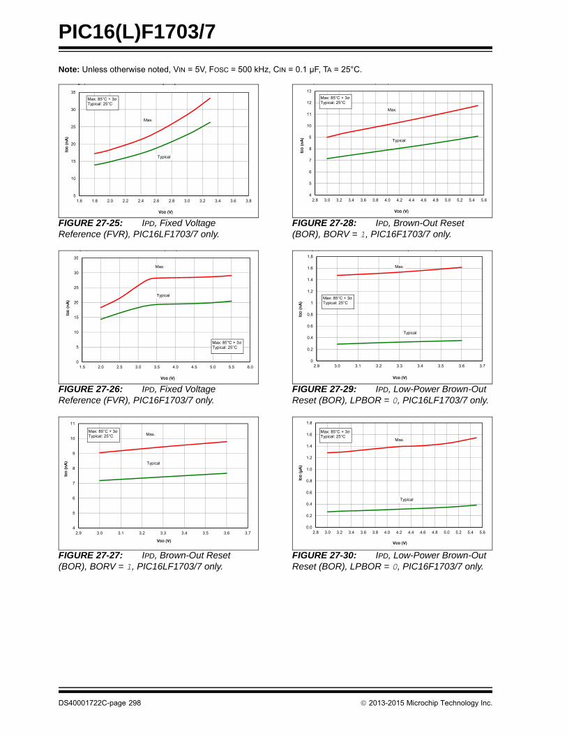
PIC16(L)F1703/7
Note: Unless otherwise noted, VIN = 5V, FOSC = 500 kHz, CIN = 0.1 µF, TA = 25°C.
FIGURE 27-25: IPD, Fixed Voltage Reference (FVR), PIC16LF1703/7 only.
FIGURE 27-26: IPD, Fixed Voltage Reference (FVR), PIC16F1703/7 only.
FIGURE 27-27: IPD, Brown-Out Reset (BOR), BORV = 1, PIC16LF1703/7 only.
FIGURE 27-28: IPD, Brown-Out Reset (BOR), BORV = 1, PIC16F1703/7 only.
FIGURE 27-29: IPD, Low-Power Brown-Out Reset (BOR), LPBOR = 0, PIC16LF1703/7 only.
FIGURE 27-30: IPD, Low-Power Brown-Out Reset (BOR), LPBOR = 0, PIC16F1703/7 only.
p , ( )
35Max: 85°C + 3Typical: 25°C
Max.
20
25
30
35
DD
(nA)
Max: 85°C + 3Typical: 25°C
Typical
10
15
20
IDD
(nA)
5
10
1.6 1.8 2.0 2.2 2.4 2.6 2.8 3.0 3.2 3.4 3.6 3.8
VDD (V)
p , ( )
Max.
35
Max.
Typical
20
25
30
35
IDD
(nA)
5
10
15
20
IDD
(nA
Max: 85°C + 3Typical: 25°C
0
5
1.5 2.0 2.5 3.0 3.5 4.0 4.5 5.0 5.5 6.0
VDD (V)
Max: 85°C + 3Typical: 25°C
Max.
11
Max: 85°C + 3Typical: 25°C Max.
Typical
7
8
9
10
11
IDD
(nA)
Max: 85°C + 3Typical: 25°C
5
6
7
8
IDD
(
4
5
2.9 3.0 3.1 3.2 3.3 3.4 3.5 3.6 3.7
VDD (V)
p ( )
12
13Max: 85°C + 3Typical: 25°C
Max.
Typical
8
9
10
11
12
13
D(n
A)
Max: 85°C + 3Typical: 25°C
Typical
5
6
7
8
9
IDD
(nA)
4
5
2.8 3.0 3.2 3.4 3.6 3.8 4.0 4.2 4.4 4.6 4.8 5.0 5.2 5.4 5.6
VDD (V)
p , ( )
Max.1.6
1.8
Max.
0.8
1
1.2
1.4
1.6
1.8
IDD
(nA)
Max: 85°C + 3Typical: 25°C
Typical
0.2
0.4
0.6
0.8
1ID
D(n
A Typical: 25 C
0
0.2
2.9 3.0 3.1 3.2 3.3 3.4 3.5 3.6 3.7
VDD (V)
1 6
1.8
Max: 85°C + 3T i l 25°C
Max.
0 8
1.0
1.2
1.4
1.6
1.8
IDD
(μA)
Max: 85°C + 3Typical: 25°C
Typical
0.2
0.4
0.6
0.8
1.0
IDD
(μA
0.0
0.2
2.8 3.0 3.2 3.4 3.6 3.8 4.0 4.2 4.4 4.6 4.8 5.0 5.2 5.4 5.6
VDD (V)
DS40001722C-page 298 2013-2015 Microchip Technology Inc.
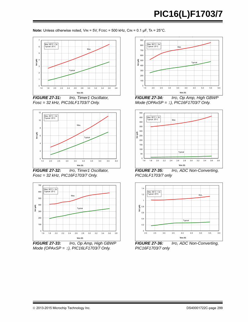
PIC16(L)F1703/7
Note: Unless otherwise noted, VIN = 5V, FOSC = 500 kHz, CIN = 0.1 µF, TA = 25°C.
FIGURE 27-31: IPD, Timer1 Oscillator, Fosc = 32 kHz, PIC16LF1703/7 Only.
FIGURE 27-32: IPD, Timer1 Oscillator, Fosc = 32 kHz, PIC16F1703/7 Only.
FIGURE 27-33: IPD, Op Amp, High GBWP Mode (OPAxSP = 1), PIC16LF1703/7 Only.
FIGURE 27-34: IPD, Op Amp, High GBWP Mode (OPAxSP = 1), PIC16F1703/7 Only.
FIGURE 27-35: IPD, ADC Non-Converting, PIC16LF1703/7 only
FIGURE 27-36: IPD, ADC Non-Converting, PIC16F1703/7 only
p
7
Max: 85°C + 3
Max.
3
4
5
6
7
IDD
(μA)
Max: 85°C + 3Typical: 25°C
Typical
1
2
3
4
IDD
(μA
0
1
1.6 1.8 2.0 2.2 2.4 2.6 2.8 3.0 3.2 3.4 3.6 3.8
VDD (V)
p , ,12
Max: 85°C + 3Typical: 25°C
Max.
Typical6
8
10
12
DD
(μA)
Max: 85°C + 3Typical: 25°C
Typical
2
4
6
IDD
(μA)
0
2
1.5 2.0 2.5 3.0 3.5 4.0 4.5 5.0 5.5 6.0
VDD (V)
700
Max: 85°C + 3
Max.
Typical
400
500
600
700
DD
(μA)
Max: 85°C + 3Typical: 25°C
Typical
100
200
300
400
IDD
(μA)
0
100
1.6 1.8 2.0 2.2 2.4 2.6 2.8 3.0 3.2 3.4 3.6 3.8
VDD (V)
p , , ( )
800
900
Max: 85°C + 3
Typical
Max.
400
500
600
700
800
900
DD
(μA)
Max: 85°C + 3Typical: 25°C
Typical
100
200
300
400
500
IDD
(μA)
0
100
1.5 2.0 2.5 3.0 3.5 4.0 4.5 5.0 5.5 6.0
VDD (V)
p , g
450
500
Max: 85°C + 3Max.
250
300
350
400
450
500
DD
(μA)
Max: 85°C + 3Typical: 25°C
Typical50
100
150
200
250ID
D(μ
A)
Typical
0
50
1.6 1.8 2.0 2.2 2.4 2.6 2.8 3.0 3.2 3.4 3.6 3.8
VDD (V)
1.4
Max.
0.8
1
1.2
1.4
DD
(μA)
Max: 85°C + 3Typical: 25°C
Typical
0.2
0.4
0.6
0.8
IDD
(μA)
0
0.2
2.0 2.5 3.0 3.5 4.0 4.5 5.0 5.5 6.0
VDD (V)
2013-2015 Microchip Technology Inc. DS40001722C-page 299
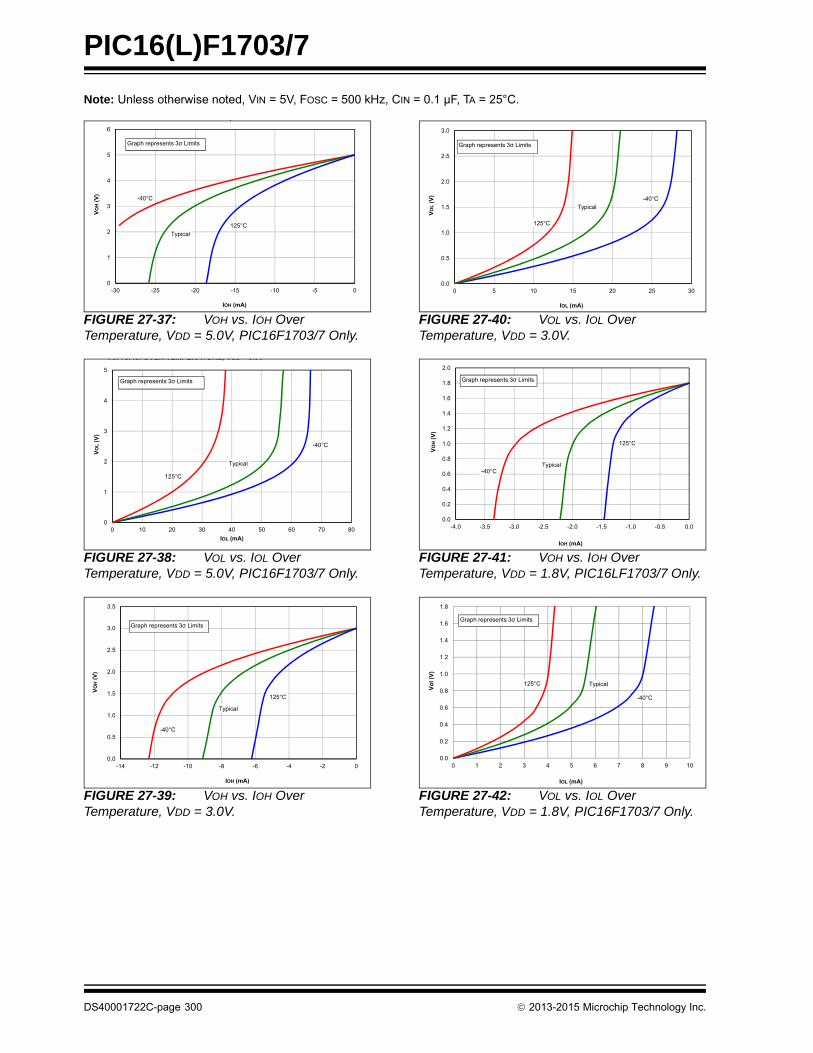
PIC16(L)F1703/7
Note: Unless otherwise noted, VIN = 5V, FOSC = 500 kHz, CIN = 0.1 µF, TA = 25°C.
FIGURE 27-37: VOH vs. IOH Over Temperature, VDD = 5.0V, PIC16F1703/7 Only.
FIGURE 27-38: VOL vs. IOL Over Temperature, VDD = 5.0V, PIC16F1703/7 Only.
FIGURE 27-39: VOH vs. IOH Over Temperature, VDD = 3.0V.
FIGURE 27-40: VOL vs. IOL Over Temperature, VDD = 3.0V.
FIGURE 27-41: VOH vs. IOH Over Temperature, VDD = 1.8V, PIC16LF1703/7 Only.
FIGURE 27-42: VOL vs. IOL Over Temperature, VDD = 1.8V, PIC16F1703/7 Only.
,
-40°C
Typical125°C
0
1
2
3
4
5
6
-30 -25 -20 -15 -10 -5 0
VOH
(V)
IOH (mA)
Graph represents 3 Limits
e Vol vs. Iol OVER TEMPERATURE, Vdd 5.0V
-40°C
Typical
125°C
0
1
2
3
4
5
0 10 20 30 40 50 60 70 80
VOL
(V)
IOL (mA)
Graph represents 3 Limits
-40°C
Typical
125°C
0.0
0.5
1.0
1.5
2.0
2.5
3.0
3.5
-14 -12 -10 -8 -6 -4 -2 0
VOH
(V)
IOH (mA)
Graph represents 3 Limits
-40°C
125°C
Typical
0.0
0.5
1.0
1.5
2.0
2.5
3.0
0 5 10 15 20 25 30
VOL
(V)
IOL (mA)
Graph represents 3 Limits
-40°CTypical
125°C
0.0
0.2
0.4
0.6
0.8
1.0
1.2
1.4
1.6
1.8
2.0
-4.0 -3.5 -3.0 -2.5 -2.0 -1.5 -1.0 -0.5 0.0
VOH
(V)
IOH (mA)
Graph represents 3 Limits
,
-40°C
Typical125°C
0.0
0.2
0.4
0.6
0.8
1.0
1.2
1.4
1.6
1.8
0 1 2 3 4 5 6 7 8 9 10
Vol (
V)
IOL (mA)
Graph represents 3 Limits
DS40001722C-page 300 2013-2015 Microchip Technology Inc.

PIC16(L)F1703/7
Note: Unless otherwise noted, VIN = 5V, FOSC = 500 kHz, CIN = 0.1 µF, TA = 25°C.
FIGURE 27-43: LFINTOSC Frequency, PIC16LF1703/7 Only.
FIGURE 27-44: LFINTOSC Frequency, PIC16F1703/7 Only.
FIGURE 27-45: WDT Time-Out Period, PIC16F1703/7 Only.
FIGURE 27-46: WDT Time-Out Period, PIC16LF1703/7 Only.
FIGURE 27-47: Brown-Out Reset Voltage, Low Trip Point (BORV = 1), PIC16LF1703/7 only.
FIGURE 27-48: Brown-Out Reset Hysteresis, Low Trip Point (BORV = 1), PIC16LF1703/7 only.
q y
Typical
Max.
Min.
20,000
22,000
24,000
26,000
28,000
30,000
32,000
34,000
36,000
38,000
40,000
1.6 1.8 2.0 2.2 2.4 2.6 2.8 3.0 3.2 3.4 3.6 3.8
Freq
uenc
y (H
z)
VDD (V)
Max: Typical + 3 (-40°C to +125°C)Typical; statistical mean @ 25°CMin: Typical - 3 (-40°C to +125°C)
q y
Typical
Max.
Min.
20,000
22,000
24,000
26,000
28,000
30,000
32,000
34,000
36,000
38,000
40,000
2.0 2.5 3.0 3.5 4.0 4.5 5.0 5.5 6.0
Freq
uenc
y (H
z)
VDD (V)
Max: Typical + 3 (-40°C to +125°C)Typical; statistical mean @ 25°CMin: Typical - 3 (-40°C to +125°C)
Typical
Max.
Min.
10
12
14
16
18
20
22
24
2.0 2.5 3.0 3.5 4.0 4.5 5.0 5.5 6.0
Tim
e (m
S)
VDD (V)
Max: Typical + 3 (-40°C to +125°C)Typical; statistical mean @ 25°CMin: Typical - 3 (-40°C to +125°C)
Typical
Max.
Min.
10
12
14
16
18
20
22
24
1.6 1.8 2 2.2 2.4 2.6 2.8 3 3.2 3.4 3.6 3.8
Tim
e (m
S)
VDD (V)
Max: Typical + 3 (-40°C to +125°C)Typical; statistical mean @ 25°CMin: Typical - 3 (-40°C to +125°C)
, ( )
Max.
Min.
Typical
1.80
1.85
1.90
1.95
2.00
-60 -40 -20 0 20 40 60 80 100 120 140
Volta
ge (V
)
Temperature (°C)
Max: Typical + 3Typical: statistical mean Min: Typical - 3
Typical
Max.
Min.
0
10
20
30
40
50
60
70
-60 -40 -20 0 20 40 60 80 100 120 140
Volta
ge (m
V)
Temperature (°C)
Max: Typical + 3Typical: statistical meanMin: Typical - 3
2013-2015 Microchip Technology Inc. DS40001722C-page 301
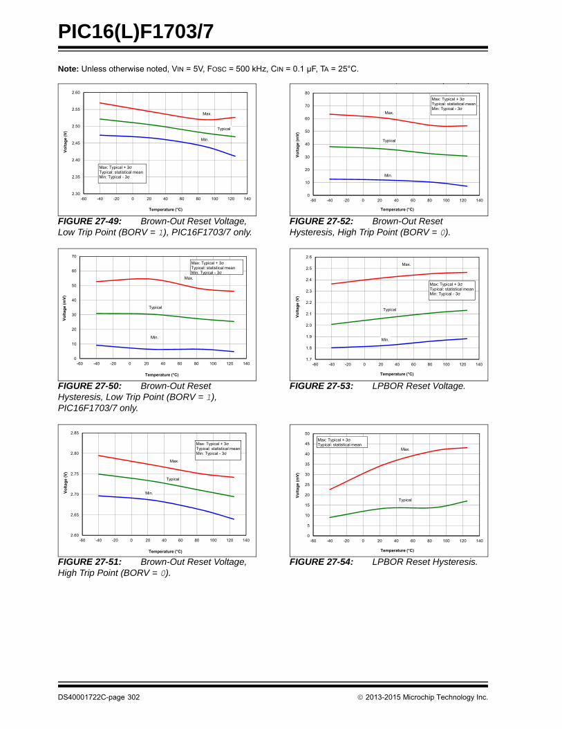
PIC16(L)F1703/7
Note: Unless otherwise noted, VIN = 5V, FOSC = 500 kHz, CIN = 0.1 µF, TA = 25°C.
FIGURE 27-49: Brown-Out Reset Voltage, Low Trip Point (BORV = 1), PIC16F1703/7 only.
FIGURE 27-50: Brown-Out Reset Hysteresis, Low Trip Point (BORV = 1), PIC16F1703/7 only.
FIGURE 27-51: Brown-Out Reset Voltage, High Trip Point (BORV = 0).
FIGURE 27-52: Brown-Out Reset Hysteresis, High Trip Point (BORV = 0).
FIGURE 27-53: LPBOR Reset Voltage.
FIGURE 27-54: LPBOR Reset Hysteresis.
Max.
Min.
Typical
2.30
2.35
2.40
2.45
2.50
2.55
2.60
-60 -40 -20 0 20 40 60 80 100 120 140
Volta
ge (V
)
Temperature (°C)
Max: Typical + 3Typical: statistical meanMin: Typical - 3
Typical
Max.
Min.
0
10
20
30
40
50
60
70
-60 -40 -20 0 20 40 60 80 100 120 140
Volta
ge (m
V)
Temperature (°C)
Max: Typical + 3Typical: statistical mean Min: Typical - 3
Max.
Min.
Typical
2.60
2.65
2.70
2.75
2.80
2.85
-60 -40 -20 0 20 40 60 80 100 120 140
Volta
ge (V
)
Temperature (°C)
Max: Typical + 3Typical: statistical meanMin: Typical - 3
, ( )
Typical
Max.
Min.
0
10
20
30
40
50
60
70
80
-60 -40 -20 0 20 40 60 80 100 120 140
Volta
ge (m
V)
Temperature (°C)
Max: Typical + 3Typical: statistical mean Min: Typical - 3
Max.
Min.
Typical
1.7
1.8
1.9
2.0
2.1
2.2
2.3
2.4
2.5
2.6
-60 -40 -20 0 20 40 60 80 100 120 140
Volta
ge (V
)
Temperature (°C)
Max: Typical + 3Typical: statistical mean Min: Typical - 3
Typical
Max.
0
5
10
15
20
25
30
35
40
45
50
-60 -40 -20 0 20 40 60 80 100 120 140
Volta
ge (m
V)
Temperature (°C)
Max: Typical + 3Typical: statistical mean
DS40001722C-page 302 2013-2015 Microchip Technology Inc.
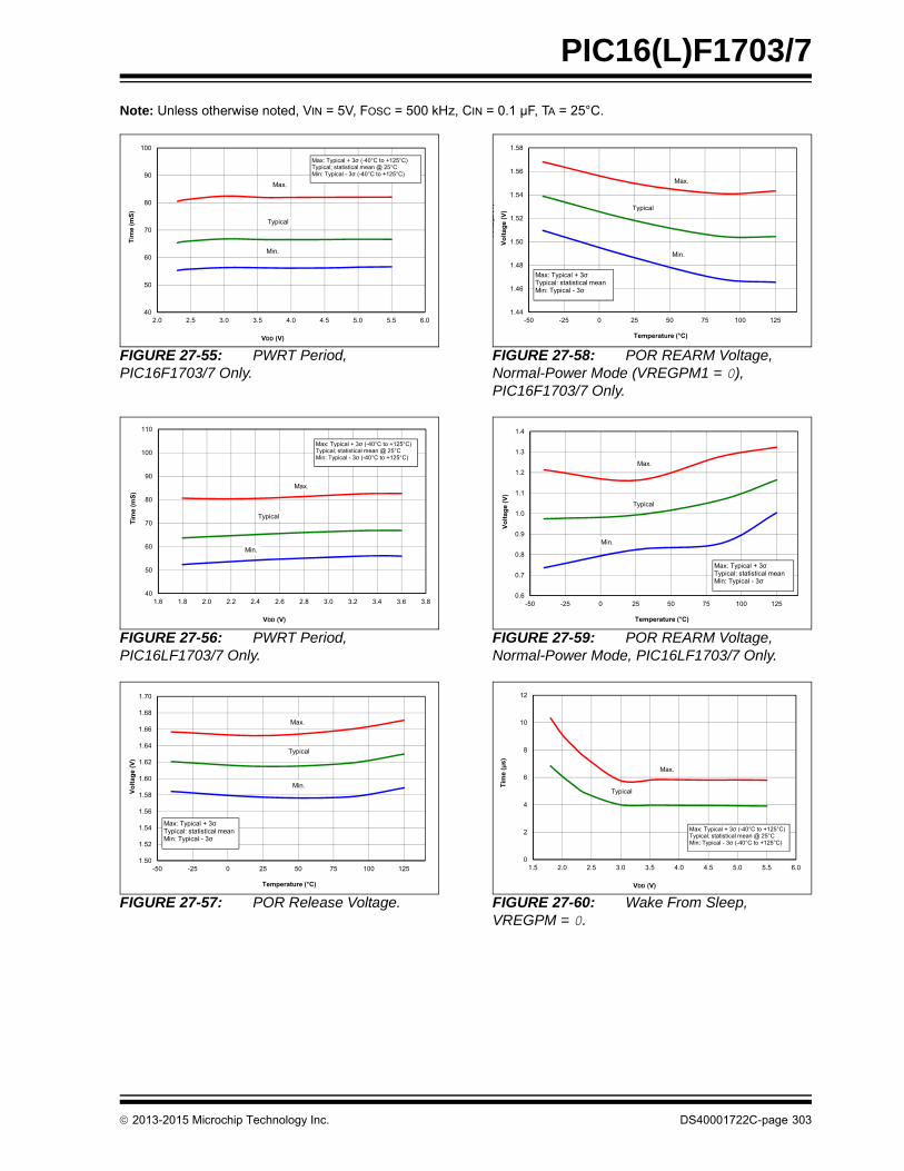
PIC16(L)F1703/7
Note: Unless otherwise noted, VIN = 5V, FOSC = 500 kHz, CIN = 0.1 µF, TA = 25°C.
FIGURE 27-55: PWRT Period, PIC16F1703/7 Only.
FIGURE 27-56: PWRT Period, PIC16LF1703/7 Only.
FIGURE 27-57: POR Release Voltage.
FIGURE 27-58: POR REARM Voltage, Normal-Power Mode (VREGPM1 = 0), PIC16F1703/7 Only.
FIGURE 27-59: POR REARM Voltage, Normal-Power Mode, PIC16LF1703/7 Only.
FIGURE 27-60: Wake From Sleep, VREGPM = 0.
Typical
Max.
Min.
40
50
60
70
80
90
100
2.0 2.5 3.0 3.5 4.0 4.5 5.0 5.5 6.0
Tim
e (m
S)
VDD (V)
Max: Typical + 3 (-40°C to +125°C)Typical; statistical mean @ 25°CMin: Typical - 3 (-40°C to +125°C)
Typical
Max.
Min.
40
50
60
70
80
90
100
110
1.6 1.8 2.0 2.2 2.4 2.6 2.8 3.0 3.2 3.4 3.6 3.8
Tim
e (m
S)
VDD (V)
Max: Typical + 3 (-40°C to +125°C)Typical; statistical mean @ 25°CMin: Typical - 3 (-40°C to +125°C)
Typical
Max.
Min.
1.50
1.52
1.54
1.56
1.58
1.60
1.62
1.64
1.66
1.68
1.70
-50 -25 0 25 50 75 100 125
Volta
ge (V
)
Temperature (°C)
Max: Typical + 3Typical: statistical meanMin: Typical - 3
1.46
1.48
1.5
1.52
1.54
1.56
1.58
-40 -20 0 20 40 60 80 100 120
Volta
ge (V
)
Temperature (°C)
Max: Typical + 3Typical: 25°C Min: Typical - 3
Typical
Max.
Min.
1.44
1.46
1.48
1.50
1.52
1.54
1.56
1.58
-50 -25 0 25 50 75 100 125
Volta
ge (V
)
Temperature (°C)
Max: Typical + 3Typical: statistical meanMin: Typical - 3
,
Typical
Max.
Min.
0.6
0.7
0.8
0.9
1.0
1.1
1.2
1.3
1.4
-50 -25 0 25 50 75 100 125
Volta
ge (V
)
Temperature (°C)
Max: Typical + 3Typical: statistical mean Min: Typical - 3
Typical
Max.
0
2
4
6
8
10
12
1.5 2.0 2.5 3.0 3.5 4.0 4.5 5.0 5.5 6.0
Tim
e (μ
s)
VDD (V)
Max: Typical + 3 (-40°C to +125°C)Typical; statistical mean @ 25°CMin: Typical - 3 (-40°C to +125°C)
2013-2015 Microchip Technology Inc. DS40001722C-page 303
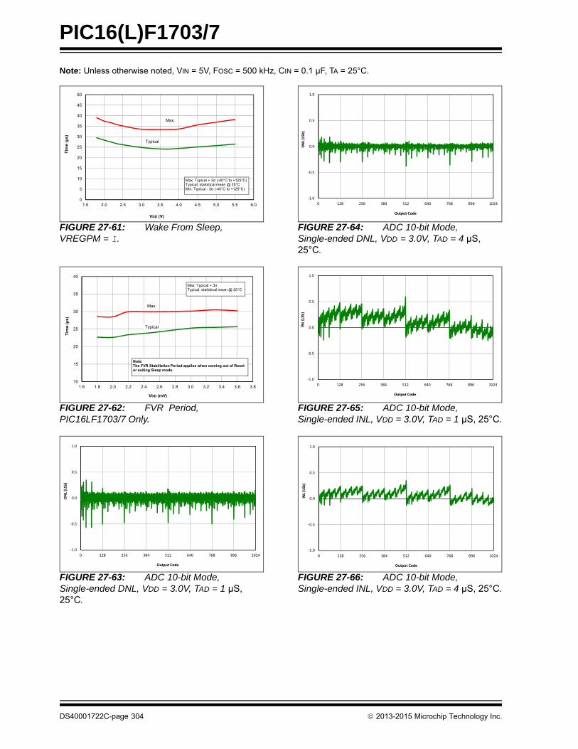
PIC16(L)F1703/7
Note: Unless otherwise noted, VIN = 5V, FOSC = 500 kHz, CIN = 0.1 µF, TA = 25°C.
FIGURE 27-61: Wake From Sleep, VREGPM = 1.
FIGURE 27-62: FVR Period, PIC16LF1703/7 Only.
FIGURE 27-63: ADC 10-bit Mode, Single-ended DNL, VDD = 3.0V, TAD = 1 µS, 25°C.
FIGURE 27-64: ADC 10-bit Mode, Single-ended DNL, VDD = 3.0V, TAD = 4 µS, 25°C.
FIGURE 27-65: ADC 10-bit Mode, Single-ended INL, VDD = 3.0V, TAD = 1 µS, 25°C.
FIGURE 27-66: ADC 10-bit Mode, Single-ended INL, VDD = 3.0V, TAD = 4 µS, 25°C.
Typical
Max.
0
5
10
15
20
25
30
35
40
45
50
1.5 2.0 2.5 3.0 3.5 4.0 4.5 5.0 5.5 6.0
Tim
e (μ
s)
VDD (V)
Max: Typical + 3 (-40°C to +125°C)Typical; statistical mean @ 25°CMin: Typical - 3 (-40°C to +125°C)
Typical
Max.
10
15
20
25
30
35
40
1.6 1.8 2.0 2.2 2.4 2.6 2.8 3.0 3.2 3.4 3.6 3.8
Tim
e (μ
s)
VDD (mV)
Max: Typical + 3Typical: statistical mean @ 25°C
Note: The FVR Stabiliztion Period applies when coming out of Reset or exiting Sleep mode.
1.0
0.5
0.0
0.5
1.0
0 128 256 384 512 640 768 896 1024
DNL(LSb)
Output CodeOutput Code
1.0
0.5
0.0
0.5
1.0
0 128 256 384 512 640 768 896 1024
DNL(LSb)
Output CodeOutput Code
1.0
0.5
0.0
0.5
1.0
0 128 256 384 512 640 768 896 1024
INL(LSb)
Output CodeOutput Code
2.0
1.5
1.0
0.5
0.0
0.5
1.0
1.5
2.0
0 512 1024 1536 2048 2560 3072 3584 4096
DNL(LSb)
Output Code
1.0
0.5
0.0
0.5
1.0
0 128 256 384 512 640 768 896 1024
INL(LSb)
Output Code
DS40001722C-page 304 2013-2015 Microchip Technology Inc.

PIC16(L)F1703/7
Note: Unless otherwise noted, VIN = 5V, FOSC = 500 kHz, CIN = 0.1 µF, TA = 25°C.
FIGURE 27-67: ADC 10-bit Mode, Single-ended DNL, VDD = 3.0V, VREF = 3.0V.
FIGURE 27-68: ADC 10-bit Mode, Single-ended INL, VDD = 3.0V, VREF = 3.0V.
FIGURE 27-69: ADC 10-bit Mode, Single-ended DNL, VDD = 3.0V, TAD = 1 µS.
FIGURE 27-70: ADC 10-bit Mode, Single-ended INL, VDD = 3.0V, TAD = 1 µS.
FIGURE 27-71: Temperature Indicator Initial Offset, High Range, Temp. = 20°C, PIC16F1703/7 only.
FIGURE 27-72: Temperature Indicator Initial Offset, Low Range, Temp. = 20°C, PIC16F1703/7 only.
Min 25°C
Min 25°C
Min 125°C
Min 40°C
Min 40°C
Min 125°C
1.5
1.0
0.5
0.0
0.5
1.0
1.5
5.00E 07 1.00E 06 2.00E 06 4.00E 06 8.00E 06
DNL(LSb)
TADs
Max 25°C
Min 25°C
Max 40°C
Min 125°CMin 40°C
Max 125°C
1.5
1.0
0.5
0.0
0.5
1.0
1.5
5.00E 07 1.00E 06 2.00E 06 4.00E 06 8.00E 06
INL(LSb)
TADs
Max 25°C
Min 25°C
Max 40°C
Min 40°C
Max 125°C
Min 125°C
1.5
1.0
0.5
0.0
0.5
1.0
1.5
1.8 2.3 3
DNL(LSb)
VREF
Max 25°C
Min 25°C
Max 40°C
Min 40°C
Max 125°C
Min 125°C
1.0
0.5
0.0
0.5
1.0
1.5
1.8 2.3 3
INL(LSb)
VREF
Typical
Max
Min
0
100
200
300
400
500
600
700
800
2.5 3.0 3.5 4.0 4.5 5.0 5.5 6.0
AD
C O
utpu
t Cod
es
VDD (V)
ADC VREF+ SET TO VDDADC VREF- SET TO GND
Max: Typical + 3Typical; statistical mean Min: Typical - 3
Typical
Max
Min
300
400
500
600
700
800
900
2.0 2.4 2.8 3.2 3.6 4.0 4.4 4.8 5.2 5.6
AD
C O
utpu
t Cod
es
VDD (V)
ADC VREF+ SET TO VDDADC VREF- SET TO GND
Max: Typical + 3Typical; statistical mean Min: Typical - 3
2013-2015 Microchip Technology Inc. DS40001722C-page 305
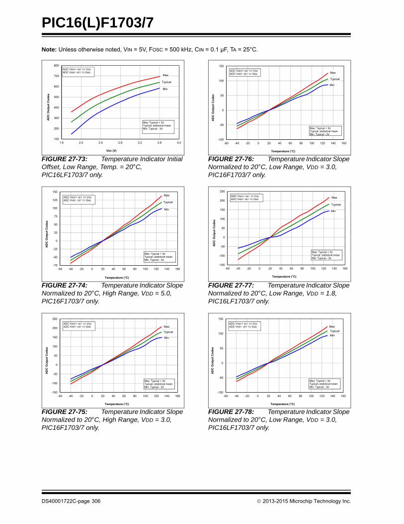
PIC16(L)F1703/7
Note: Unless otherwise noted, VIN = 5V, FOSC = 500 kHz, CIN = 0.1 µF, TA = 25°C.
FIGURE 27-73: Temperature Indicator Initial Offset, Low Range, Temp. = 20°C, PIC16LF1703/7 only.
FIGURE 27-74: Temperature Indicator Slope Normalized to 20°C, High Range, VDD = 5.0, PIC16F1703/7 only.
FIGURE 27-75: Temperature Indicator Slope Normalized to 20°C, High Range, VDD = 3.0, PIC16F1703/7 only.
FIGURE 27-76: Temperature Indicator Slope Normalized to 20°C, Low Range, VDD = 3.0, PIC16F1703/7 only.
FIGURE 27-77: Temperature Indicator Slope Normalized to 20°C, Low Range, VDD = 1.8, PIC16LF1703/7 only.
FIGURE 27-78: Temperature Indicator Slope Normalized to 20°C, Low Range, VDD = 3.0, PIC16LF1703/7 only.
Typical
Max
Min
100
200
300
400
500
600
700
800
1.6 2.0 2.4 2.8 3.2 3.6 4.0
AD
C O
utpu
t Cod
es
VDD (V)
ADC VREF+ SET TO VDDADC VREF- SET TO GND
Max: Typical + 3Typical; statistical mean Min: Typical - 3
Typical
Max
Min
-75
-50
-25
0
25
50
75
100
125
150
-60 -40 -20 0 20 40 60 80 100 120 140 160
AD
C O
utpu
t Cod
es
Temperature (°C)
ADC VREF+ SET TO VDDADC VREF- SET TO GND
Max: Typical + 3Typical; statistical mean Min: Typical - 3
Typical
Max
Min
-150
-100
-50
0
50
100
150
200
250
-60 -40 -20 0 20 40 60 80 100 120 140 160
AD
C O
utpu
t Cod
es
Temperature (°C)
ADC VREF+ SET TO VDDADC VREF- SET TO GND
Max: Typical + 3Typical; statistical mean Min: Typical - 3
Typical
Max
Min
-100
-50
0
50
100
150
-60 -40 -20 0 20 40 60 80 100 120 140 160
AD
C O
utpu
t Cod
es
Temperature (°C)
ADC VREF+ SET TO VDDADC VREF- SET TO GND
Max: Typical + 3Typical; statistical mean Min: Typical - 3
Typical
Max
Min
-150
-100
-50
0
50
100
150
200
250
-60 -40 -20 0 20 40 60 80 100 120 140 160
AD
C O
utpu
t Cod
es
Temperature (°C)
ADC VREF+ SET TO VDDADC VREF- SET TO GND
Max: Typical + 3Typical; statistical mean Min: Typical - 3
TypicalMax
Min
-100
-50
0
50
100
150
-60 -40 -20 0 20 40 60 80 100 120 140 160
AD
C O
utpu
t Cod
es
Temperature (°C)
ADC VREF+ SET TO VDDADC VREF- SET TO GND
Max: Typical + 3Typical; statistical mean Min: Typical - 3
DS40001722C-page 306 2013-2015 Microchip Technology Inc.

PIC16(L)F1703/7
Note: Unless otherwise noted, VIN = 5V, FOSC = 500 kHz, CIN = 0.1 µF, TA = 25°C.
FIGURE 27-79: Temperature Indicator Slope Normalized to 20°C, High Range, VDD = 3.0, PIC16LF1703/7 only.
FIGURE 27-80: Op Amp, Common-Mode Rejection Ratio (CMRR), VDD = 3.0V
FIGURE 27-81: Op Amp, Offset Voltage Histogram, VDD = 3.0V, VCM = VDD/2
FIGURE 27-82: Op Amp, Offset Over Common-Mode Voltage, VDD = 3.0V, Temp. = 25°C
FIGURE 27-83: Op Amp, Offset Over Common-Mode Voltage, VDD = 5.0V, Temp. = 25°C, PIC16F1703/7 only.
FIGURE 27-84: Op Amp, Output Slew Rate, Rising Edge, PIC16LF1703/7 only.
Typical
Max
Min
-150
-100
-50
0
50
100
150
200
250
-60 -40 -20 0 20 40 60 80 100 120 140 160
AD
C O
utpu
t Cod
es
Temperature (°C)
Max: Typical + 3Typical; statistical mean Min: Typical - 3
ADC VREF+ SET TO VDDADC VREF- SET TO GND
Min
Typical
Max
40
45
50
55
60
65
70
75
80
-50 -30 -10 10 30 50 70 90 110 130
CM
RR
(dB
)
Temperature (°C)
Max: Typical + 3Typical; statistical meanMin: Typical - 3
, , ,
0%
5%
10%
15%
20%
25%
30%
35%
-7 -5 -4 -3 -2 -1 0 1 2 3 4 5 6 7
Perc
ent o
f Uni
ts
Offset Voltage (mV)
-40°C
25°C
85°C
125°C
Sample Size = 3,200
g p
Min
Typical
Max
-8
-6
-4
-2
0
2
4
6
8
0.0 0.3 0.6 0.9 1.2 1.5 1.8 2.1 2.4 2.7 3.0
Offs
et V
olta
ge (V
)
Common Mode Voltage (V)
Max: Typical + 3Typical; statistical meanMin: Typical - 3
Min
Typical
Max
-8
-6
-4
-2
0
2
4
6
8
0.0 0.5 1.0 1.5 2.0 2.5 3.0 3.5 4.0 4.5 5.0
Offs
et V
olta
ge (V
)
Common Mode Voltage (V)
Max: Typical + 3Typical; statistical meanMin: Typical - 3
, ,
VDD = 2.3V
VDD = 3V
VDD = 3.6V
7.20
7.25
7.30
7.35
7.40
7.45
7.50
7.55
7.60
7.65
7.70
7.75
-60 -40 -20 0 20 40 60 80 100 120 140
Slew
Rat
e (V
/μs)
VDD (V)
2013-2015 Microchip Technology Inc. DS40001722C-page 307
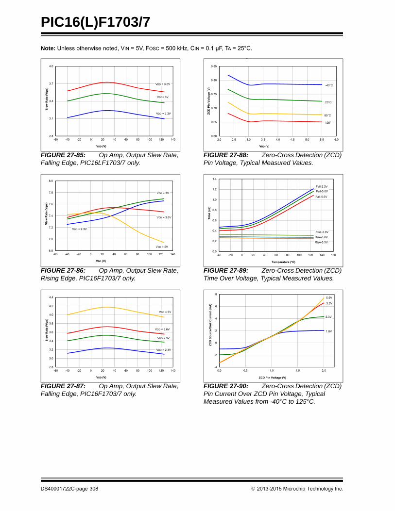
PIC16(L)F1703/7
Note: Unless otherwise noted, VIN = 5V, FOSC = 500 kHz, CIN = 0.1 µF, TA = 25°C.
FIGURE 27-85: Op Amp, Output Slew Rate, Falling Edge, PIC16LF1703/7 only.
FIGURE 27-86: Op Amp, Output Slew Rate, Rising Edge, PIC16F1703/7 only.
FIGURE 27-87: Op Amp, Output Slew Rate, Falling Edge, PIC16F1703/7 only.
FIGURE 27-88: Zero-Cross Detection (ZCD) Pin Voltage, Typical Measured Values.
FIGURE 27-89: Zero-Cross Detection (ZCD) Time Over Voltage, Typical Measured Values.
FIGURE 27-90: Zero-Cross Detection (ZCD) Pin Current Over ZCD Pin Voltage, Typical Measured Values from -40°C to 125°C.
VDD = 2.3V
VDD= 3V
VDD = 3.6V
2.8
3.1
3.4
3.7
4.0
-60 -40 -20 0 20 40 60 80 100 120 140
Slew
Rat
e (V
/μs)
VDD (V)
VDD = 2.3V
VDD = 3V
VDD = 3.6V
VDD = 5V6.8
7.0
7.2
7.4
7.6
7.8
8.0
-60 -40 -20 0 20 40 60 80 100 120 140
Slew
Rat
e (V
/μs)
VDD (V)
VDD = 2.3V
VDD = 3V
VDD = 3.6V
VDD = 5V
2.8
3.0
3.2
3.4
3.6
3.8
4.0
4.2
4.4
-60 -40 -20 0 20 40 60 80 100 120 140
Slew
Rat
e (V
/μs)
VDD (V)
g ,
-40°C
25°C
125°
85°C
0.60
0.65
0.70
0.75
0.80
0.85
2.0 2.5 3.0 3.5 4.0 4.5 5.0 5.5 6.0
ZCD
Pin
Vol
tage
(V)
VDD (V)
Fall-2.3VFall-3.0V
Fall-5.5V
Rise-2.3V
Rise-3.0V
Rise-5.5V
0.0
0.2
0.4
0.6
0.8
1.0
1.2
1.4
-40 -20 0 20 40 60 80 100 120 140 160
Tim
e (u
s)
Temperature (°C)
1.8V
2.3V
3.0V
5.5V
-4
-2
0
2
4
6
8
0.0 0.5 1.0 1.5 2.0
ZCD
Sou
rce/
Sink
Cur
rent
(mA
)
ZCD Pin Voltage (V)
DS40001722C-page 308 2013-2015 Microchip Technology Inc.

PIC16(L)F1703/7
Note: Unless otherwise noted, VIN = 5V, FOSC = 500 kHz, CIN = 0.1 µF, TA = 25°C.
FIGURE 27-91: Zero-Cross Detection (ZCD) Pin Response Time Over Current, Typical Measured Values from -40°C to 125°C.
1.8V
2.3V3.0V
5.5V0.1
0.2
0.3
0.4
0.5
0.6
0.7
0.8
0.9
1.0
0 50 100 150 200 250 300 350 400 450 500
Tim
e (u
s)
ZCD Source/Sink Current (uA)
2013-2015 Microchip Technology Inc. DS40001722C-page 309
PIC16(L)F1703/7
28.0 DEVELOPMENT SUPPORT
The PIC® microcontrollers (MCU) and dsPIC® digitalsignal controllers (DSC) are supported with a full rangeof software and hardware development tools:
• Integrated Development Environment
- MPLAB® X IDE Software
• Compilers/Assemblers/Linkers
- MPLAB XC Compiler
- MPASMTM Assembler
- MPLINKTM Object Linker/MPLIBTM Object Librarian
- MPLAB Assembler/Linker/Librarian forVarious Device Families
• Simulators
- MPLAB X SIM Software Simulator
• Emulators
- MPLAB REAL ICE™ In-Circuit Emulator
• In-Circuit Debuggers/Programmers
- MPLAB ICD 3
- PICkit™ 3
• Device Programmers
- MPLAB PM3 Device Programmer
• Low-Cost Demonstration/Development Boards, Evaluation Kits and Starter Kits
• Third-party development tools
28.1 MPLAB X Integrated Development Environment Software
The MPLAB X IDE is a single, unified graphical userinterface for Microchip and third-party software, andhardware development tool that runs on Windows®,Linux and Mac OS® X. Based on the NetBeans IDE,MPLAB X IDE is an entirely new IDE with a host of freesoftware components and plug-ins for high-performance application development and debugging.Moving between tools and upgrading from softwaresimulators to hardware debugging and programmingtools is simple with the seamless user interface.
With complete project management, visual call graphs,a configurable watch window and a feature-rich editorthat includes code completion and context menus,MPLAB X IDE is flexible and friendly enough for newusers. With the ability to support multiple tools onmultiple projects with simultaneous debugging, MPLABX IDE is also suitable for the needs of experiencedusers.
Feature-Rich Editor:
• Color syntax highlighting
• Smart code completion makes suggestions and provides hints as you type
• Automatic code formatting based on user-defined rules
• Live parsing
User-Friendly, Customizable Interface:
• Fully customizable interface: toolbars, toolbar buttons, windows, window placement, etc.
• Call graph window
Project-Based Workspaces:
• Multiple projects
• Multiple tools
• Multiple configurations
• Simultaneous debugging sessions
File History and Bug Tracking:
• Local file history feature
• Built-in support for Bugzilla issue tracker
DS40001722C-page 310 2013-2015 Microchip Technology Inc.
PIC16(L)F1703/7
28.2 MPLAB XC Compilers
The MPLAB XC Compilers are complete ANSI Ccompilers for all of Microchip’s 8, 16, and 32-bit MCUand DSC devices. These compilers provide powerfulintegration capabilities, superior code optimization andease of use. MPLAB XC Compilers run on Windows,Linux or MAC OS X.
For easy source level debugging, the compilers providedebug information that is optimized to the MPLAB XIDE.
The free MPLAB XC Compiler editions support alldevices and commands, with no time or memoryrestrictions, and offer sufficient code optimization formost applications.
MPLAB XC Compilers include an assembler, linker andutilities. The assembler generates relocatable objectfiles that can then be archived or linked with other relo-catable object files and archives to create an execut-able file. MPLAB XC Compiler uses the assembler toproduce its object file. Notable features of the assem-bler include:
• Support for the entire device instruction set
• Support for fixed-point and floating-point data
• Command-line interface
• Rich directive set
• Flexible macro language
• MPLAB X IDE compatibility
28.3 MPASM Assembler
The MPASM Assembler is a full-featured, universalmacro assembler for PIC10/12/16/18 MCUs.
The MPASM Assembler generates relocatable objectfiles for the MPLINK Object Linker, Intel® standard HEXfiles, MAP files to detail memory usage and symbolreference, absolute LST files that contain source linesand generated machine code, and COFF files fordebugging.
The MPASM Assembler features include:
• Integration into MPLAB X IDE projects
• User-defined macros to streamline assembly code
• Conditional assembly for multipurpose source files
• Directives that allow complete control over the assembly process
28.4 MPLINK Object Linker/MPLIB Object Librarian
The MPLINK Object Linker combines relocatableobjects created by the MPASM Assembler. It can linkrelocatable objects from precompiled libraries, usingdirectives from a linker script.
The MPLIB Object Librarian manages the creation andmodification of library files of precompiled code. Whena routine from a library is called from a source file, onlythe modules that contain that routine will be linked inwith the application. This allows large libraries to beused efficiently in many different applications.
The object linker/library features include:
• Efficient linking of single libraries instead of many smaller files
• Enhanced code maintainability by grouping related modules together
• Flexible creation of libraries with easy module listing, replacement, deletion and extraction
28.5 MPLAB Assembler, Linker and Librarian for Various Device Families
MPLAB Assembler produces relocatable machinecode from symbolic assembly language for PIC24,PIC32 and dsPIC DSC devices. MPLAB XC Compileruses the assembler to produce its object file. Theassembler generates relocatable object files that canthen be archived or linked with other relocatable objectfiles and archives to create an executable file. Notablefeatures of the assembler include:
• Support for the entire device instruction set
• Support for fixed-point and floating-point data
• Command-line interface
• Rich directive set
• Flexible macro language
• MPLAB X IDE compatibility
2013-2015 Microchip Technology Inc. DS40001722C-page 311
PIC16(L)F1703/7
28.6 MPLAB X SIM Software Simulator
The MPLAB X SIM Software Simulator allows codedevelopment in a PC-hosted environment by simulat-ing the PIC MCUs and dsPIC DSCs on an instructionlevel. On any given instruction, the data areas can beexamined or modified and stimuli can be applied froma comprehensive stimulus controller. Registers can belogged to files for further run-time analysis. The tracebuffer and logic analyzer display extend the power ofthe simulator to record and track program execution,actions on I/O, most peripherals and internal registers.
The MPLAB X SIM Software Simulator fully supportssymbolic debugging using the MPLAB XC Compilers,and the MPASM and MPLAB Assemblers. The soft-ware simulator offers the flexibility to develop anddebug code outside of the hardware laboratory envi-ronment, making it an excellent, economical softwaredevelopment tool.
28.7 MPLAB REAL ICE In-Circuit Emulator System
The MPLAB REAL ICE In-Circuit Emulator System isMicrochip’s next generation high-speed emulator forMicrochip Flash DSC and MCU devices. It debugs andprograms all 8, 16 and 32-bit MCU, and DSC deviceswith the easy-to-use, powerful graphical user interface ofthe MPLAB X IDE.
The emulator is connected to the design engineer’sPC using a high-speed USB 2.0 interface and isconnected to the target with either a connectorcompatible with in-circuit debugger systems (RJ-11)or with the new high-speed, noise tolerant, Low-Voltage Differential Signal (LVDS) interconnection(CAT5).
The emulator is field upgradeable through future firm-ware downloads in MPLAB X IDE. MPLAB REAL ICEoffers significant advantages over competitive emulatorsincluding full-speed emulation, run-time variablewatches, trace analysis, complex breakpoints, logicprobes, a ruggedized probe interface and long (up tothree meters) interconnection cables.
28.8 MPLAB ICD 3 In-Circuit Debugger System
The MPLAB ICD 3 In-Circuit Debugger System isMicrochip’s most cost-effective, high-speed hardwaredebugger/programmer for Microchip Flash DSC andMCU devices. It debugs and programs PIC Flashmicrocontrollers and dsPIC DSCs with the powerful,yet easy-to-use graphical user interface of the MPLABIDE.
The MPLAB ICD 3 In-Circuit Debugger probe isconnected to the design engineer’s PC using a high-speed USB 2.0 interface and is connected to the targetwith a connector compatible with the MPLAB ICD 2 orMPLAB REAL ICE systems (RJ-11). MPLAB ICD 3supports all MPLAB ICD 2 headers.
28.9 PICkit 3 In-Circuit Debugger/Programmer
The MPLAB PICkit 3 allows debugging and program-ming of PIC and dsPIC Flash microcontrollers at a mostaffordable price point using the powerful graphical userinterface of the MPLAB IDE. The MPLAB PICkit 3 isconnected to the design engineer’s PC using a full-speed USB interface and can be connected to the tar-get via a Microchip debug (RJ-11) connector (compati-ble with MPLAB ICD 3 and MPLAB REAL ICE). Theconnector uses two device I/O pins and the Reset lineto implement in-circuit debugging and In-Circuit SerialProgramming™ (ICSP™).
28.10 MPLAB PM3 Device Programmer
The MPLAB PM3 Device Programmer is a universal,CE compliant device programmer with programmablevoltage verification at VDDMIN and VDDMAX formaximum reliability. It features a large LCD display(128 x 64) for menus and error messages, and a mod-ular, detachable socket assembly to support variouspackage types. The ICSP cable assembly is includedas a standard item. In Stand-Alone mode, the MPLABPM3 Device Programmer can read, verify and programPIC devices without a PC connection. It can also setcode protection in this mode. The MPLAB PM3connects to the host PC via an RS-232 or USB cable.The MPLAB PM3 has high-speed communications andoptimized algorithms for quick programming of largememory devices, and incorporates an MMC card for filestorage and data applications.
DS40001722C-page 312 2013-2015 Microchip Technology Inc.
PIC16(L)F1703/7
28.11 Demonstration/Development Boards, Evaluation Kits, and Starter Kits
A wide variety of demonstration, development andevaluation boards for various PIC MCUs and dsPICDSCs allows quick application development on fullyfunctional systems. Most boards include prototypingareas for adding custom circuitry and provide applica-tion firmware and source code for examination andmodification.
The boards support a variety of features, including LEDs,temperature sensors, switches, speakers, RS-232interfaces, LCD displays, potentiometers and additionalEEPROM memory.
The demonstration and development boards can beused in teaching environments, for prototyping customcircuits and for learning about various microcontrollerapplications.
In addition to the PICDEM™ and dsPICDEM™demonstration/development board series of circuits,Microchip has a line of evaluation kits and demonstra-tion software for analog filter design, KEELOQ® securityICs, CAN, IrDA®, PowerSmart battery management,SEEVAL® evaluation system, Sigma-Delta ADC, flowrate sensing, plus many more.
Also available are starter kits that contain everythingneeded to experience the specified device. This usuallyincludes a single application and debug capability, allon one board.
Check the Microchip web page (www.microchip.com)for the complete list of demonstration, developmentand evaluation kits.
28.12 Third-Party Development Tools
Microchip also offers a great collection of tools fromthird-party vendors. These tools are carefully selectedto offer good value and unique functionality.
• Device Programmers and Gang Programmers from companies, such as SoftLog and CCS
• Software Tools from companies, such as Gimpel and Trace Systems
• Protocol Analyzers from companies, such as Saleae and Total Phase
• Demonstration Boards from companies, such as MikroElektronika, Digilent® and Olimex
• Embedded Ethernet Solutions from companies, such as EZ Web Lynx, WIZnet and IPLogika®
2013-2015 Microchip Technology Inc. DS40001722C-page 313
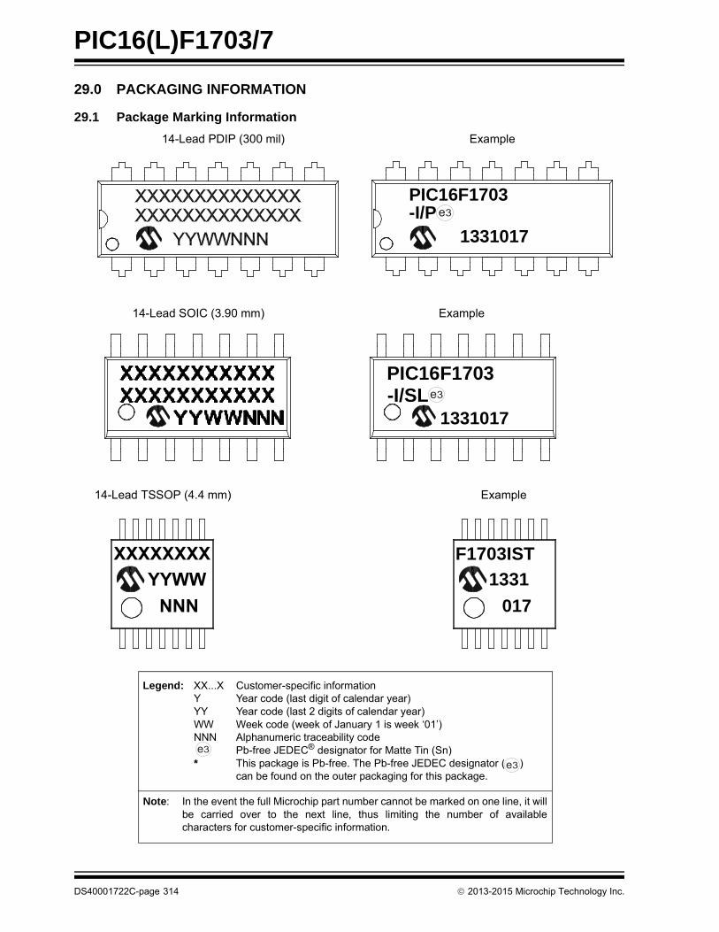
PIC16(L)F1703/7
29.0 PACKAGING INFORMATION
29.1 Package Marking Information
Legend: XX...X Customer-specific informationY Year code (last digit of calendar year)YY Year code (last 2 digits of calendar year)WW Week code (week of January 1 is week ‘01’)NNN Alphanumeric traceability code Pb-free JEDEC® designator for Matte Tin (Sn)* This package is Pb-free. The Pb-free JEDEC designator ( )
can be found on the outer packaging for this package.
Note: In the event the full Microchip part number cannot be marked on one line, it willbe carried over to the next line, thus limiting the number of availablecharacters for customer-specific information.
3e
3e
28-Lead SOIC (7.50 mm) Example
14-Lead PDIP (300 mil) Example
14-Lead SOIC (3.90 mm) Example
1331017
3e
PIC16F1703-I/P
PIC16F1703-I/SL
1331017
3e
14-Lead TSSOP (4.4 mm) Example
YYWWNNN
XXXXXXXX F1703IST
1331
017
DS40001722C-page 314 2013-2015 Microchip Technology Inc.

PIC16(L)F1703/7
Package Marking Information (Continued)
16-Lead QFN (4x4x0.9 mm) Example
PIN 1 PIN 1
20-Lead SSOP (5.30 mm) Example
PIC16F1703
3310173e-I/ML
20-Lead PDIP (300 mil) Example
XXXXXXXXXXXXXXXXXXXXXXXXXXXXXXXXXX
YYWWNNN
PIC16F1707-E/P
1331017
3e
PIC16F1707-E/SS
1331017
3e
20-Lead SOIC (7.50 mm) Example
PIC16F1707-E/SO
1331017
3e
2013-2015 Microchip Technology Inc. DS40001722C-page 315
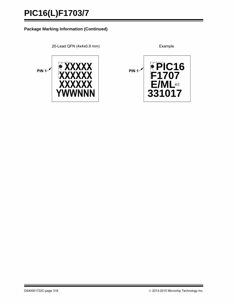
PIC16(L)F1703/7
Package Marking Information (Continued)
20-Lead QFN (4x4x0.9 mm) Example
PIN 1 PIN 1 PIC16F1707
3310173eE/ML
DS40001722C-page 316 2013-2015 Microchip Technology Inc.
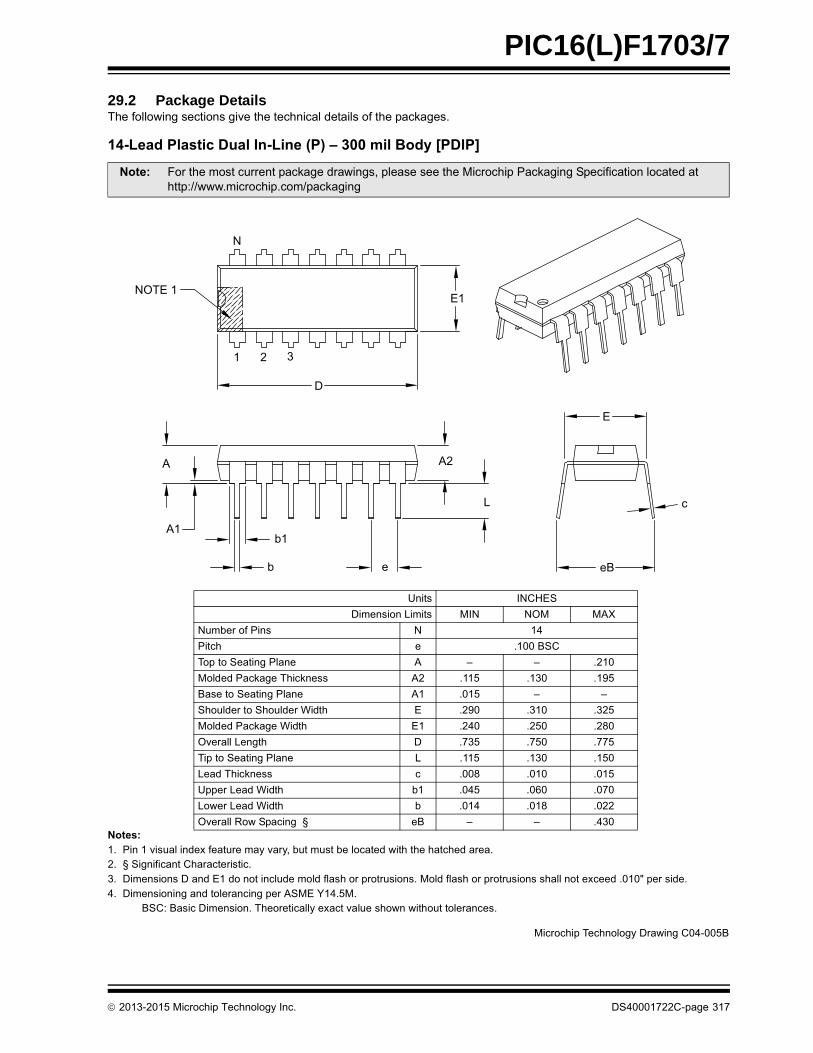
PIC16(L)F1703/7
29.2 Package DetailsThe following sections give the technical details of the packages.
���������� ������������������������������
�� �� �� �������� !�����"�#�$��%!��&������'�(!%�&! %�(�����%�"�)�%��%�����%���"�����
�� *������$����%�+����%�� %���
,� ��&�� �� �����"�-��"��%�����!"��&�"�$�� ����%! �� ����"�$�� ����%! �� � ������%��#���"�����.���� �"��
�� ��&�� ��������"�%���������������-�/���0��
1�+2�1� �����&�� ���� ���%��������#��%����!�� �)��)�%�!%�%������ �
�� � 3�%���& %��!��%����4����"�)��� '����� �� ���%��������������4�����������$���%������%�"��%�
�%%�255)))�&��������&5���4�����
6��% �7+8-�
��&�� ���9�&�% ��7 7:� ��;
7!&(��$���� 7 ��
��%�� � �����1�+
��%����%��������� � < < ����
��"�"����4���� ���4�� �� ���0 ��,� ���0
1� ��%����%��������� �� ���0 < <
��!�"��%���!�"��=�"%� - ���� �,�� �,�0
��"�"����4����=�"%� -� ���� ��0� ��>�
:������9���%� � ��,0 ��0� ���0
���%����%��������� 9 ���0 ��,� ��0�
9��"� ���4�� � ���> ���� ���0
6����9��"�=�"%� (� ���0 ��?� ����
9)��9��"�=�"%� ( ���� ���> ����
:�������)����������* �1 < < ��,�
N
E1
D
NOTE 1
1 2 3
E
c
eB
A2
L
A
A1b1
b e
������� ������� ��)��� +�����01
2013-2015 Microchip Technology Inc. DS40001722C-page 317
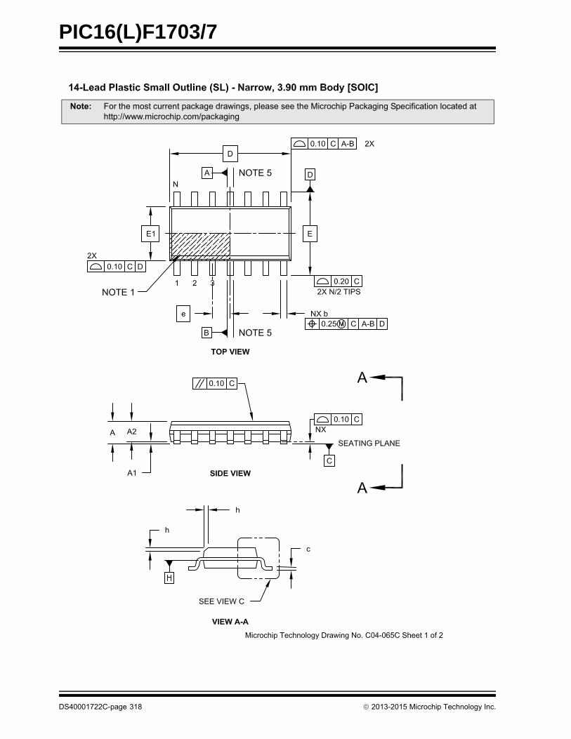
PIC16(L)F1703/7
Note: For the most current package drawings, please see the Microchip Packaging Specification located at http://www.microchip.com/packaging
DS40001722C-page 318 2013-2015 Microchip Technology Inc.
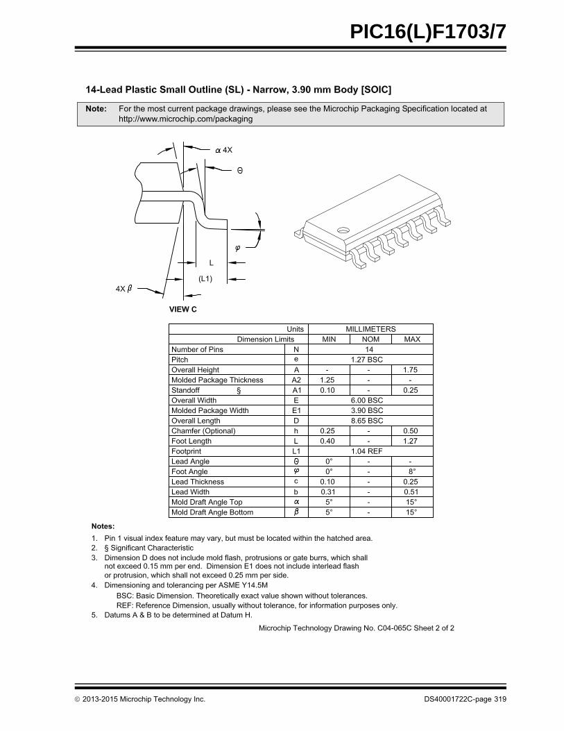
PIC16(L)F1703/7
Note: For the most current package drawings, please see the Microchip Packaging Specification located at http://www.microchip.com/packaging
2013-2015 Microchip Technology Inc. DS40001722C-page 319
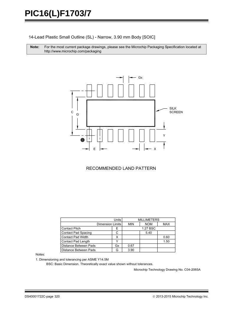
PIC16(L)F1703/7
�� � 3�%���& %��!��%����4����"�)��� '����� �� ���%��������������4�����������$���%������%�"��%�
�%%�255)))�&��������&5���4�����
DS40001722C-page 320 2013-2015 Microchip Technology Inc.
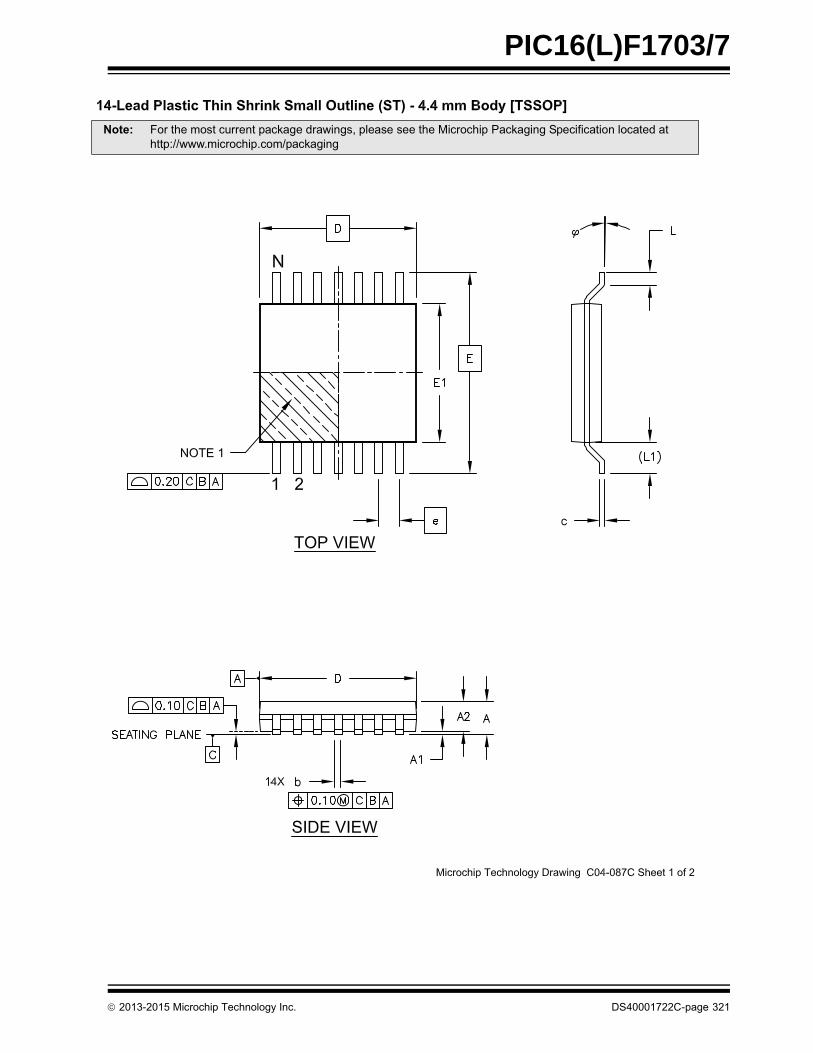
PIC16(L)F1703/7
Note: For the most current package drawings, please see the Microchip Packaging Specification located at
http://www.microchip.com/packaging
2013-2015 Microchip Technology Inc. DS40001722C-page 321
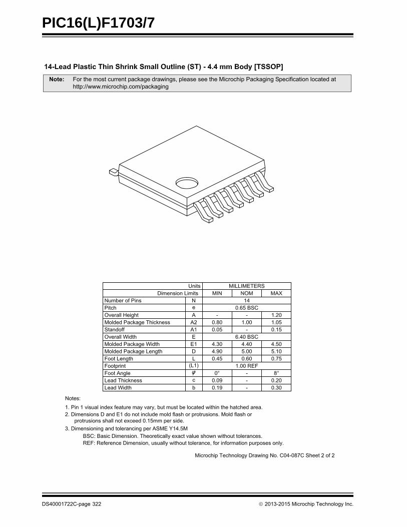
PIC16(L)F1703/7
Note: For the most current package drawings, please see the Microchip Packaging Specification located at
http://www.microchip.com/packaging
DS40001722C-page 322 2013-2015 Microchip Technology Inc.
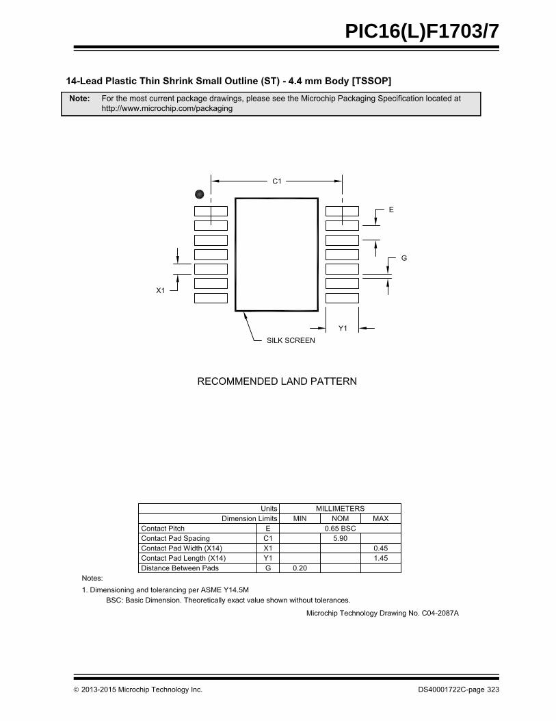
PIC16(L)F1703/7
Note: For the most current package drawings, please see the Microchip Packaging Specification located at http://www.microchip.com/packaging
2013-2015 Microchip Technology Inc. DS40001722C-page 323
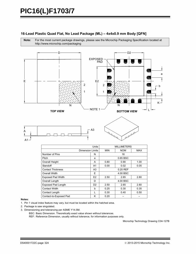
PIC16(L)F1703/7
�!�������� ��"���#�� $��������%�&��'����(�(�)*�������"#��
�� �� �� �������� !�����"�#�$��%!��&������'�(!%�&! %�(�����%�"�)�%����%�����%���"�����
�� ���4����� � �)� ���!��%�"�
,� ��&�� ��������"�%���������������-�/���0��
1�+2 1� �����&�� ���� ���%��������#��%����!�� �)��)�%�!%�%������ �
�-32 ��$��������&�� ��'�! !�����)�%�!%�%������'�$���$&�%����!� � �����
�� � 3�%���& %��!��%����4����"�)��� '����� �� ���%��������������4�����������$���%������%�"��%�
�%%�255)))�&��������&5���4�����
6��% ��99��- -��
��&�� ���9�&�% ��7 7:� ��;
7!&(��$���� 7 �?
��%�� � ��?0�1�+
:������8����% � ��>� ���� ����
�%��"$$� �� ���� ���� ���0
+�%��%� ���4�� �, ������-3
:������=�"%� - �����1�+
-#� �"���"�=�"%� -� ��0� ��?0 ��>�
:������9���%� � �����1�+
-#� �"���"�9���%� �� ��0� ��?0 ��>�
+�%��%�=�"%� ( ���0 ��,� ��,0
+�%��%�9���%� 9 ��,� ���� ��0�
+�%��%�%�-#� �"���" V ���� < <
D
E
N
2
1
EXPOSEDPAD
D2
E22
1
e
b
KN
NOTE 1
A3
A1
A
LTOP VIEW BOTTOM VIEW
������� ������� ��)��� +������1
DS40001722C-page 324 2013-2015 Microchip Technology Inc.
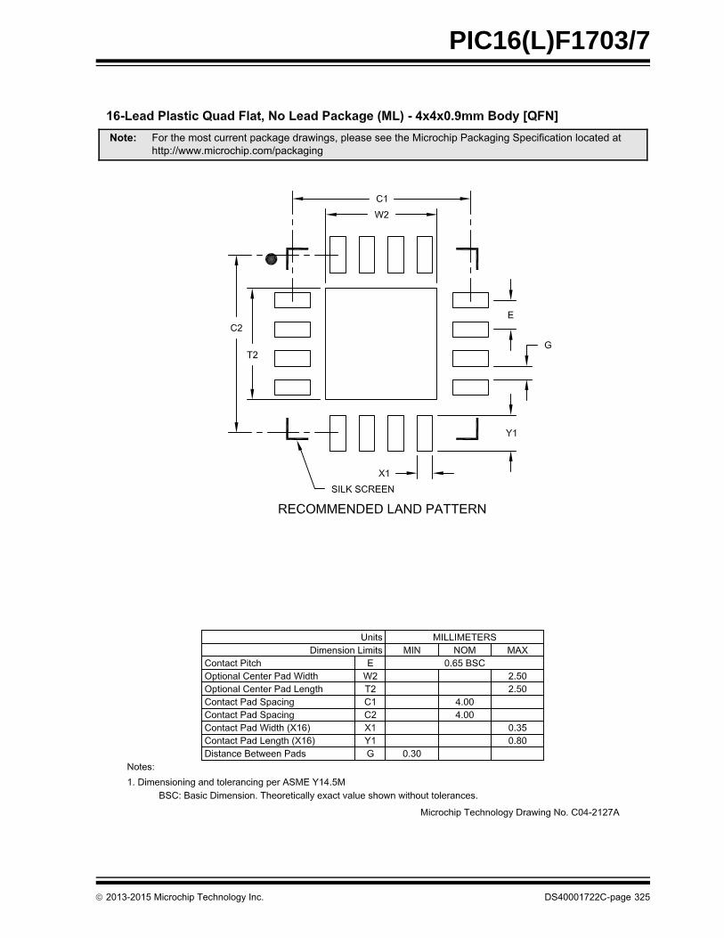
PIC16(L)F1703/7
Note: For the most current package drawings, please see the Microchip Packaging Specification located at http://www.microchip.com/packaging
2013-2015 Microchip Technology Inc. DS40001722C-page 325
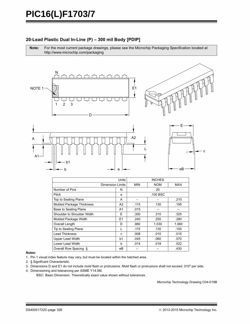
PIC16(L)F1703/7
+��������� ������������������������������
�
�� �� �� �������� !�����"�#�$��%!��&������'�(!%�&! %�(�����%�"�)�%����%�����%���"�����
�� *������$����%�+����%�� %���
,� ��&�� �� �����"�-��"��%�����!"��&�"�$�� ����%! �� ����"�$�� ����%! �� � ������%��#���"�����.���� �"��
�� ��&�� ��������"�%���������������-�/���0��
1�+2 1� �����&�� ���� ���%��������#��%����!�� �)��)�%�!%�%������ �
�� � 3�%���& %��!��%����4����"�)��� '����� �� ���%��������������4�����������$���%������%�"��%�
�%%�255)))�&��������&5���4�����
6��% �7+8-�
��&�� ���9�&�% ��7 7:� ��;
7!&(��$���� 7 ��
��%�� � �����1�+
��%����%��������� � < < ����
��"�"����4���� ���4�� �� ���0 ��,� ���0
1� ��%����%��������� �� ���0 < <
��!�"��%���!�"��=�"%� - �,�� �,�� �,�0
��"�"����4����=�"%� -� ���� ��0� ��>�
:������9���%� � ��>� ���,� ���?�
���%����%��������� 9 ���0 ��,� ��0�
9��"� ���4�� � ���> ���� ���0
6����9��"�=�"%� (� ���0 ��?� ����
9)��9��"�=�"%� ( ���� ���> ����
:�������)����������* �1 < < ��,�
N
E1NOTE 1
D
1 2 3
A
A1
A2
L
e
b1
b
E
c
eB
������� ������� ��)��� +������1
DS40001722C-page 326 2013-2015 Microchip Technology Inc.

PIC16(L)F1703/7
+��������� ��,-.��%,����/� �����,,��0)���������,,/�
�� �� �� �������� !�����"�#�$��%!��&������'�(!%�&! %�(�����%�"�)�%����%�����%���"�����
�� ��&�� �� �����"�-��"��%�����!"��&�"�$�� ����%! �� ����"�$�� ����%! �� � ������%��#���"������&&���� �"��
,� ��&�� ��������"�%���������������-�/���0��
1�+2 1� �����&�� ���� ���%��������#��%����!�� �)��)�%�!%�%������ �
�-32 ��$��������&�� ��'�! !�����)�%�!%�%������'�$���$&�%����!� � �����
�� � 3�%���& %��!��%����4����"�)��� '����� �� ���%��������������4�����������$���%������%�"��%�
�%%�255)))�&��������&5���4�����
6��% ��99��- -��
��&�� ���9�&�% ��7 7:� ��;
7!&(��$���� 7 ��
��%�� � ��?0�1�+
:������8����% � < < ����
��"�"����4���� ���4�� �� ��?0 ���0 ��>0
�%��"$$� �� ���0 < <
:������=�"%� - ���� ��>� >���
��"�"����4����=�"%� -� 0��� 0�,� 0�?�
:������9���%� � ?��� ���� ��0�
3%�9���%� 9 ��00 ���0 ���0
3%���% 9� ���0��-3
9��"� ���4�� � ���� < ���0
3%������ � �W �W >W
9��"�=�"%� ( ���� < ��,>
φ
LL1
A2c
eb
A1
A
1 2
NOTE 1
E1
E
D
N
������� ������� ��)��� +������1
2013-2015 Microchip Technology Inc. DS40001722C-page 327
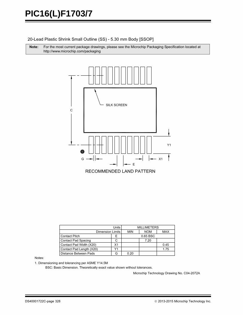
PIC16(L)F1703/7
Note: For the most current package drawings, please see the Microchip Packaging Specification located at http://www.microchip.com/packaging
DS40001722C-page 328 2013-2015 Microchip Technology Inc.
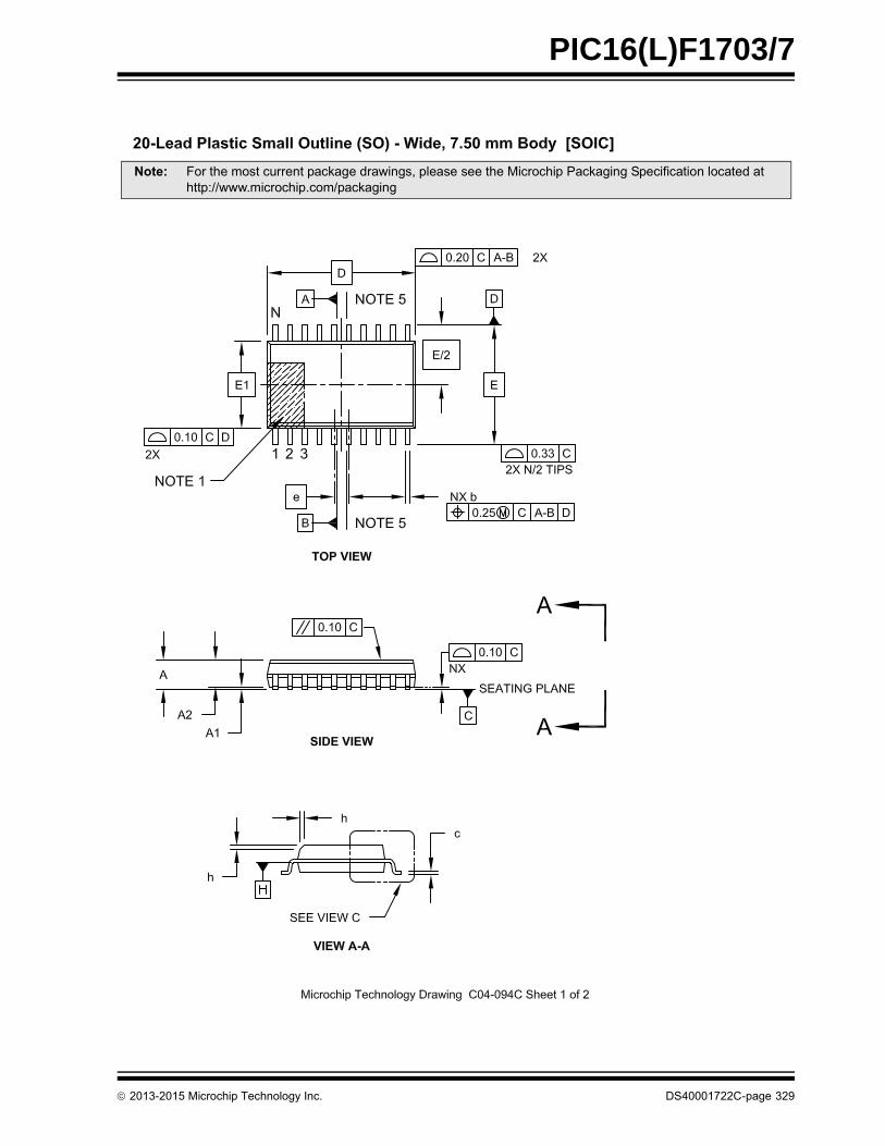
PIC16(L)F1703/7
Note: For the most current package drawings, please see the Microchip Packaging Specification located at http://www.microchip.com/packaging
2013-2015 Microchip Technology Inc. DS40001722C-page 329
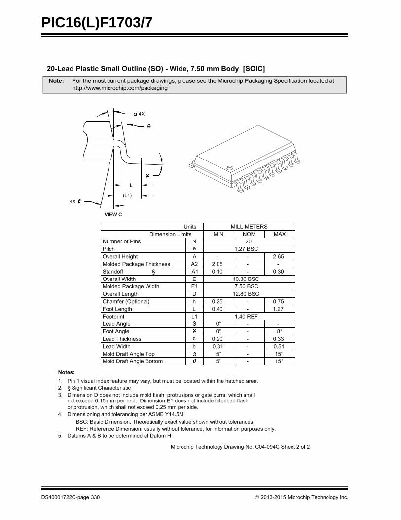
PIC16(L)F1703/7
Note: For the most current package drawings, please see the Microchip Packaging Specification located at http://www.microchip.com/packaging
DS40001722C-page 330 2013-2015 Microchip Technology Inc.
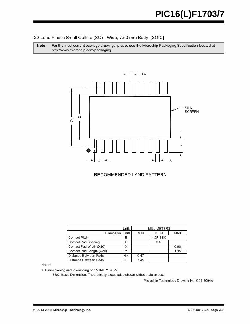
PIC16(L)F1703/7
Note: For the most current package drawings, please see the Microchip Packaging Specification located at http://www.microchip.com/packaging
2013-2015 Microchip Technology Inc. DS40001722C-page 331
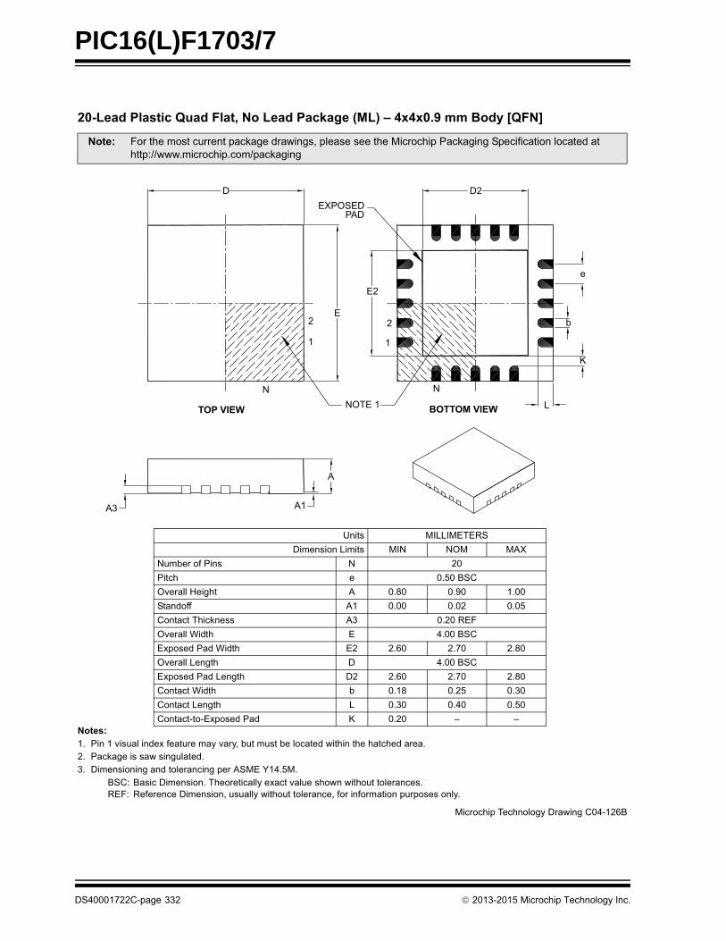
PIC16(L)F1703/7
+��������� ��"���#�� $��������%�&��'����(�(�)*�������"#��
�
�� �� �� �������� !�����"�#�$��%!��&������'�(!%�&! %�(�����%�"�)�%����%�����%���"�����
�� ���4����� � �)� ���!��%�"�
,� ��&�� ��������"�%���������������-�/���0��
1�+2 1� �����&�� ���� ���%��������#��%����!�� �)��)�%�!%�%������ �
�-32 ��$��������&�� ��'�! !�����)�%�!%�%������'�$���$&�%����!� � �����
�� � 3�%���& %��!��%����4����"�)��� '����� �� ���%��������������4�����������$���%������%�"��%�
�%%�255)))�&��������&5���4�����
6��% ��99��- -��
��&�� ���9�&�% ��7 7:� ��;
7!&(��$���� 7 ��
��%�� � ��0��1�+
:������8����% � ��>� ���� ����
�%��"$$� �� ���� ���� ���0
+�%��%� ���4�� �, ������-3
:������=�"%� - �����1�+
-#� �"���"�=�"%� -� ��?� ���� ��>�
:������9���%� � �����1�+
-#� �"���"�9���%� �� ��?� ���� ��>�
+�%��%�=�"%� ( ���> ���0 ��,�
+�%��%�9���%� 9 ��,� ���� ��0�
+�%��%�%�-#� �"���" V ���� < <
DEXPOSED
PAD
E
E2
2
1
N
TOP VIEW NOTE 1
N
L
K
b
e
D2
2
1
A
A1A3
BOTTOM VIEW
������� ������� ��)��� +�����?1
DS40001722C-page 332 2013-2015 Microchip Technology Inc.

PIC16(L)F1703/7
�� � 3�%���& %��!��%����4����"�)��� '����� �� ���%��������������4�����������$���%������%�"��%�
�%%�255)))�&��������&5���4�����
2013-2015 Microchip Technology Inc. DS40001722C-page 333
PIC16(L)F1703/7
DS40001722C-page 334 2013-2015 Microchip Technology Inc.
APPENDIX A: DATA SHEET REVISION HISTORY
Revision A (10/2013)
Initial release of this document.
Revision B (02/2015)
Changed from Preliminary to Final data sheet.
Added Section 3.2: High-Endurance Flash.
Removed Figures 6-3, 6-4, 6-6, 6-10.
Removed Sections 6.2.1.2, 6.2.1.3, 6.2.1.6, 6.3.2, 6.4,6.4.2, 6.5.
Replaced Section 18.0.
Updated Figures 2-1, 6-1, 6-2, 6-10, 7-2, 7-3, 14-1,16-1, 17-1.
Updated PIC16(L)F170x Family Types Table.
Updated Registers 4-1, 6-1, 6-2, 14-1, 16-1, 16-2, 17-1.
Updated Section 23.0 from SSP to SSPx.
Updated Sections 6.1, 6.2, 6.2.1, 6.2.1.1, 6.2.2,6.2.2.1, 6.2.2.2, 6.2.2.4, 6.2.2.6, 6.3.1, 8.2.2, 11.3.6,16.1.3, 17.0, 17.1, 17.1.1.
Updated Tables 1, 2, 1-2, 1-3, 3-1, 6-1, 6-2, 26-18.
Revision C (09/2015)
Added High Endurance Flash Data Memory (HEF)bullet on front page. Updated PIC16(L)F170x FamilyTypes Table. Updated graphs 27-63 through 27-70.

2013-2015 Microchip Technology Inc. DS40001722C-page 335
PIC16(L)F1703/7
THE MICROCHIP WEB SITE
Microchip provides online support via our web site atwww.microchip.com. This web site is used as a meansto make files and information easily available tocustomers. Accessible by using your favorite Internetbrowser, the web site contains the followinginformation:
• Product Support – Data sheets and errata, application notes and sample programs, design resources, user’s guides and hardware support documents, latest software releases and archived software
• General Technical Support – Frequently Asked Questions (FAQ), technical support requests, online discussion groups, Microchip consultant program member listing
• Business of Microchip – Product selector and ordering guides, latest Microchip press releases, listing of seminars and events, listings of Microchip sales offices, distributors and factory representatives
CUSTOMER CHANGE NOTIFICATION SERVICE
Microchip’s customer notification service helps keepcustomers current on Microchip products. Subscriberswill receive e-mail notification whenever there arechanges, updates, revisions or errata related to aspecified product family or development tool of interest.
To register, access the Microchip web site atwww.microchip.com. Under “Support”, click on“Customer Change Notification” and follow theregistration instructions.
CUSTOMER SUPPORT
Users of Microchip products can receive assistancethrough several channels:
• Distributor or Representative
• Local Sales Office
• Field Application Engineer (FAE)
• Technical Support
Customers should contact their distributor,representative or Field Application Engineer (FAE) forsupport. Local sales offices are also available to helpcustomers. A listing of sales offices and locations isincluded in the back of this document.
Technical support is available through the web siteat: http://www.microchip.com/support
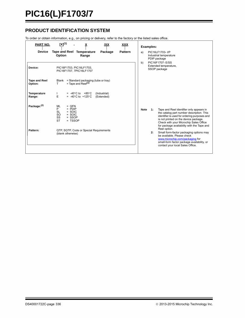
PIC16(L)F1703/7
DS40001722C-page 336 2013-2015 Microchip Technology Inc.
PRODUCT IDENTIFICATION SYSTEM
To order or obtain information, e.g., on pricing or delivery, refer to the factory or the listed sales office.
PART NO. X /XX XXX
PatternPackageTemperatureRange
Device
Device: PIC16F1703, PIC16LF1703,PIC16F1707, 7PIC16LF1707
Tape and Reel Option:
Blank = Standard packaging (tube or tray) T = Tape and Reel(1)
Temperature Range:
I = -40C to +85C (Industrial)E = -40C to +125C (Extended)
Package:(2) ML = QFNP = PDIPSL = SOICSO = SOICSS = SSOPST = TSSOP
Pattern: QTP, SQTP, Code or Special Requirements (blank otherwise)
Examples:
a) PIC16LF1703- I/PIndustrial temperaturePDIP package
b) PIC16F1707- E/SSExtended temperature,SSOP package
Note 1: Tape and Reel identifier only appears in the catalog part number description. This identifier is used for ordering purposes and is not printed on the device package. Check with your Microchip Sales Office for package availability with the Tape and Reel option.
2: Small form-factor packaging options may be available. Please check www.microchip.com/packaging for small-form factor package availability, or contact your local Sales Office.
[X](1)
Tape and ReelOption
-
Note the following details of the code protection feature on Microchip devices:
• Microchip products meet the specification contained in their particular Microchip Data Sheet.
• Microchip believes that its family of products is one of the most secure families of its kind on the market today, when used in the intended manner and under normal conditions.
• There are dishonest and possibly illegal methods used to breach the code protection feature. All of these methods, to our knowledge, require using the Microchip products in a manner outside the operating specifications contained in Microchip’s Data Sheets. Most likely, the person doing so is engaged in theft of intellectual property.
• Microchip is willing to work with the customer who is concerned about the integrity of their code.
• Neither Microchip nor any other semiconductor manufacturer can guarantee the security of their code. Code protection does not mean that we are guaranteeing the product as “unbreakable.”
Code protection is constantly evolving. We at Microchip are committed to continuously improving the code protection features of ourproducts. Attempts to break Microchip’s code protection feature may be a violation of the Digital Millennium Copyright Act. If such actsallow unauthorized access to your software or other copyrighted work, you may have a right to sue for relief under that Act.
Information contained in this publication regarding deviceapplications and the like is provided only for your convenienceand may be superseded by updates. It is your responsibility toensure that your application meets with your specifications.MICROCHIP MAKES NO REPRESENTATIONS ORWARRANTIES OF ANY KIND WHETHER EXPRESS ORIMPLIED, WRITTEN OR ORAL, STATUTORY OROTHERWISE, RELATED TO THE INFORMATION,INCLUDING BUT NOT LIMITED TO ITS CONDITION,QUALITY, PERFORMANCE, MERCHANTABILITY ORFITNESS FOR PURPOSE. Microchip disclaims all liabilityarising from this information and its use. Use of Microchipdevices in life support and/or safety applications is entirely atthe buyer’s risk, and the buyer agrees to defend, indemnify andhold harmless Microchip from any and all damages, claims,suits, or expenses resulting from such use. No licenses areconveyed, implicitly or otherwise, under any Microchipintellectual property rights unless otherwise stated.
2013-2015 Microchip Technology Inc.
QUALITY MANAGEMENT SYSTEM CERTIFIED BY DNV
== ISO/TS 16949 ==
Trademarks
The Microchip name and logo, the Microchip logo, dsPIC, FlashFlex, flexPWR, JukeBlox, KEELOQ, KEELOQ logo, Kleer, LANCheck, MediaLB, MOST, MOST logo, MPLAB, OptoLyzer, PIC, PICSTART, PIC32 logo, RightTouch, SpyNIC, SST, SST Logo, SuperFlash and UNI/O are registered trademarks of Microchip Technology Incorporated in the U.S.A. and other countries.
The Embedded Control Solutions Company and mTouch are registered trademarks of Microchip Technology Incorporated in the U.S.A.
Analog-for-the-Digital Age, BodyCom, chipKIT, chipKIT logo, CodeGuard, dsPICDEM, dsPICDEM.net, ECAN, In-Circuit Serial Programming, ICSP, Inter-Chip Connectivity, KleerNet, KleerNet logo, MiWi, motorBench, MPASM, MPF, MPLAB Certified logo, MPLIB, MPLINK, MultiTRAK, NetDetach, Omniscient Code Generation, PICDEM, PICDEM.net, PICkit, PICtail, RightTouch logo, REAL ICE, SQI, Serial Quad I/O, Total Endurance, TSHARC, USBCheck, VariSense, ViewSpan, WiperLock, Wireless DNA, and ZENA are trademarks of Microchip Technology Incorporated in the U.S.A. and other countries.
SQTP is a service mark of Microchip Technology Incorporated in the U.S.A.
Silicon Storage Technology is a registered trademark of Microchip Technology Inc. in other countries.
GestIC is a registered trademark of Microchip Technology Germany II GmbH & Co. KG, a subsidiary of Microchip Technology Inc., in other countries.
All other trademarks mentioned herein are property of their respective companies.
© 2013-2015, Microchip Technology Incorporated, Printed in the U.S.A., All Rights Reserved.
ISBN: 978-1-63277-846-8
Microchip received ISO/TS-16949:2009 certification for its worldwide
DS40001722C-page 337
headquarters, design and wafer fabrication facilities in Chandler and Tempe, Arizona; Gresham, Oregon and design centers in California and India. The Company’s quality system processes and procedures are for its PIC® MCUs and dsPIC® DSCs, KEELOQ® code hopping devices, Serial EEPROMs, microperipherals, nonvolatile memory and analog products. In addition, Microchip’s quality system for the design and manufacture of development systems is ISO 9001:2000 certified.

DS40001722C-page 338 2013-2015 Microchip Technology Inc.
AMERICASCorporate Office2355 West Chandler Blvd.Chandler, AZ 85224-6199Tel: 480-792-7200 Fax: 480-792-7277Technical Support: http://www.microchip.com/supportWeb Address: www.microchip.com
AtlantaDuluth, GA Tel: 678-957-9614 Fax: 678-957-1455
Austin, TXTel: 512-257-3370
BostonWestborough, MA Tel: 774-760-0087 Fax: 774-760-0088
ChicagoItasca, IL Tel: 630-285-0071 Fax: 630-285-0075
ClevelandIndependence, OH Tel: 216-447-0464 Fax: 216-447-0643
DallasAddison, TX Tel: 972-818-7423 Fax: 972-818-2924
DetroitNovi, MI Tel: 248-848-4000
Houston, TX Tel: 281-894-5983
IndianapolisNoblesville, IN Tel: 317-773-8323Fax: 317-773-5453
Los AngelesMission Viejo, CA Tel: 949-462-9523 Fax: 949-462-9608
New York, NY Tel: 631-435-6000
San Jose, CA Tel: 408-735-9110
Canada - TorontoTel: 905-673-0699 Fax: 905-673-6509
ASIA/PACIFICAsia Pacific OfficeSuites 3707-14, 37th FloorTower 6, The GatewayHarbour City, Kowloon
Hong KongTel: 852-2943-5100Fax: 852-2401-3431
Australia - SydneyTel: 61-2-9868-6733Fax: 61-2-9868-6755
China - BeijingTel: 86-10-8569-7000 Fax: 86-10-8528-2104
China - ChengduTel: 86-28-8665-5511Fax: 86-28-8665-7889
China - ChongqingTel: 86-23-8980-9588Fax: 86-23-8980-9500
China - DongguanTel: 86-769-8702-9880
China - HangzhouTel: 86-571-8792-8115 Fax: 86-571-8792-8116
China - Hong Kong SARTel: 852-2943-5100 Fax: 852-2401-3431
China - NanjingTel: 86-25-8473-2460Fax: 86-25-8473-2470
China - QingdaoTel: 86-532-8502-7355Fax: 86-532-8502-7205
China - ShanghaiTel: 86-21-5407-5533 Fax: 86-21-5407-5066
China - ShenyangTel: 86-24-2334-2829Fax: 86-24-2334-2393
China - ShenzhenTel: 86-755-8864-2200 Fax: 86-755-8203-1760
China - WuhanTel: 86-27-5980-5300Fax: 86-27-5980-5118
China - XianTel: 86-29-8833-7252Fax: 86-29-8833-7256
ASIA/PACIFICChina - XiamenTel: 86-592-2388138 Fax: 86-592-2388130
China - ZhuhaiTel: 86-756-3210040 Fax: 86-756-3210049
India - BangaloreTel: 91-80-3090-4444 Fax: 91-80-3090-4123
India - New DelhiTel: 91-11-4160-8631Fax: 91-11-4160-8632
India - PuneTel: 91-20-3019-1500
Japan - OsakaTel: 81-6-6152-7160 Fax: 81-6-6152-9310
Japan - TokyoTel: 81-3-6880- 3770 Fax: 81-3-6880-3771
Korea - DaeguTel: 82-53-744-4301Fax: 82-53-744-4302
Korea - SeoulTel: 82-2-554-7200Fax: 82-2-558-5932 or 82-2-558-5934
Malaysia - Kuala LumpurTel: 60-3-6201-9857Fax: 60-3-6201-9859
Malaysia - PenangTel: 60-4-227-8870Fax: 60-4-227-4068
Philippines - ManilaTel: 63-2-634-9065Fax: 63-2-634-9069
SingaporeTel: 65-6334-8870Fax: 65-6334-8850
Taiwan - Hsin ChuTel: 886-3-5778-366Fax: 886-3-5770-955
Taiwan - KaohsiungTel: 886-7-213-7828
Taiwan - TaipeiTel: 886-2-2508-8600 Fax: 886-2-2508-0102
Thailand - BangkokTel: 66-2-694-1351Fax: 66-2-694-1350
EUROPEAustria - WelsTel: 43-7242-2244-39Fax: 43-7242-2244-393
Denmark - CopenhagenTel: 45-4450-2828 Fax: 45-4485-2829
France - ParisTel: 33-1-69-53-63-20 Fax: 33-1-69-30-90-79
Germany - DusseldorfTel: 49-2129-3766400
Germany - KarlsruheTel: 49-721-625370
Germany - MunichTel: 49-89-627-144-0 Fax: 49-89-627-144-44
Italy - Milan Tel: 39-0331-742611 Fax: 39-0331-466781
Italy - VeniceTel: 39-049-7625286
Netherlands - DrunenTel: 31-416-690399 Fax: 31-416-690340
Poland - WarsawTel: 48-22-3325737
Spain - MadridTel: 34-91-708-08-90Fax: 34-91-708-08-91
Sweden - StockholmTel: 46-8-5090-4654
UK - WokinghamTel: 44-118-921-5800Fax: 44-118-921-5820
Worldwide Sales and Service
07/14/15