Embed Size (px)
Citation preview
PIC16(L)F722/3/4/6/728/40/44-Pin Flash Microcontrollers with XLP Technology
Devices Included In This Data Sheet:
PIC16F722/3/4/6/7 Devices:
PIC16LF722/3/4/6/7 Devices:
High-Performance RISC CPU:
• Only 35 Instructions to Learn:- All single-cycle instructions except branches
• Operating Speed:- DC – 20 MHz oscillator/clock input- DC – 200 ns instruction cycle
• Up to 8K x 14 Words of Flash Program Memory• Up to 368 Bytes of Data Memory (RAM)• Interrupt Capability• 8-Level Deep Hardware Stack• Direct, Indirect and Relative Addressing modes• Processor Read Access to Program Memory• Pinout Compatible to other 28/40-pin PIC16CXXX
and PIC16FXXX Microcontrollers
Special Microcontroller Features:
• Precision Internal Oscillator:- 16 MHz or 500 kHz operation- Factory calibrated to ±1%, typical- Software tunable- Software selectable ÷1, ÷2, ÷4 or ÷8 divider
• 1.8V-5.5V Operation – PIC16F722/3/4/6/7• 1.8V-3.6V Operation – PIC16LF722/3/4/6/7• Power-on Reset (POR), Power-up Timer (PWRT)
and Oscillator Start-up Timer (OST)• Brown-out Reset (BOR):
- Selectable between two trip points- Disable in Sleep option
• Programmable Code Protection• In-Circuit Serial ProgrammingTM (ICSPTM) via Two
Pins• Multiplexed Master Clear with Pull-up/Input Pin• Industrial and Extended Temperature Range• High-Endurance Flash Cell:
- 1,000 write Flash endurance (typical)- Flash retention: > 40 years
• Power-Saving Sleep mode
Extreme Low-Power Management PIC16LF722/3/4/6/7 with XLP:
• Sleep Mode: 20 nA• Watchdog Timer: 500 nA • Timer1 Oscillator: 600 nA @ 32 kHz
Analog Features:
• A/D Converter:- 8-bit resolution and up to 14 channels- Conversion available during Sleep- Selectable 1.024/2.048/4.096V voltage
reference
• On-chip 3.2V Regulator (PIC16F722/3/4/6/7 devices only)
Peripheral Highlights:
• Up to 35 I/O Pins and One Input-only Pin:- High-current source/sink for direct LED drive- Interrupt-on-pin change- Individually programmable weak pull-ups
• Timer0: 8-Bit Timer/Counter with 8-Bit Prescaler• Enhanced Timer1:
- Dedicated low-power 32 kHz oscillator- 16-bit timer/counter with prescaler- External Gate Input mode with Toggle and
Single Shot modes - Interrupt-on-gate completion
• Timer2: 8-Bit Timer/Counter with 8-Bit Period Register, Prescaler and Postscaler
• Two Capture, Compare, PWM (CCP) Modules:- 16-bit Capture, max. resolution 12.5 ns- 16-bit Compare, max. resolution 200 ns- 10-bit PWM, max. frequency 20 kHz
• Addressable Universal Synchronous Asynchronous Receiver Transmitter (AUSART)
• Synchronous Serial Port (SSP):
- SPI (Master/Slave)
- I2C (Slave) with Address Mask
• mTouch® Sensing Oscillator Module:- Up to 16 input channels
• PIC16F722 • PIC16F726
• PIC16F723 • PIC16F727
• PIC16F724
• PIC16LF722 • PIC16LF726
• PIC16LF723 • PIC16LF727
• PIC16LF724
2007-2015 Microchip Technology Inc. DS40001341F-page 1

PIC16(L)F722/3/4/6/7
PIC16(L)F72X Family Types
Device
Dat
a S
hee
t In
dex
Pro
gra
m M
emo
ryF
las
h (
wo
rds
)
Dat
a S
RA
M(b
yte
s)
Hig
h-E
nd
ura
nc
e F
lash
M
em
ory
(b
yte
s)
I/O
’s(2
)
8-b
it A
DC
(ch
)
Ca
pS
ens
e (c
h)
Tim
ers
(8/1
6-b
it)
AU
SA
RT
SS
P (
I2 C/S
PI)
CC
P
Deb
ug
(1)
XL
P
PIC16(L)F707 (1) 8192 363 0 36 14 32 4/2 1 1 2 I Y
PIC16(L)F720 (2) 2048 128 128 18 12 — 2/1 1 1 1 I Y
PIC16(L)F721 (2) 4096 256 128 18 12 — 2/1 1 1 1 I Y
PIC16(L)F722 (4) 2048 128 0 25 11 8 2/1 1 1 2 I Y
PIC16(L)F722A (3) 2048 128 0 25 11 8 2/1 1 1 2 I Y
PIC16(L)F723 (4) 4096 192 0 25 11 8 2/1 1 1 2 I Y
PIC16(L)F723A (3) 4096 192 0 25 11 8 2/1 1 1 2 I Y
PIC16(L)F724 (4) 4096 192 0 36 14 16 2/1 1 1 2 I Y
PIC16(L)F726 (4) 8192 368 0 25 11 8 2/1 1 1 2 I Y
PIC16(L)F727 (4) 8192 368 0 36 14 16 2/1 1 1 2 I Y
Note 1: I - Debugging, Integrated on Chip; H - Debugging, Requires Debug Header.2: One pin is input-only.
Data Sheet Index: (Unshaded devices are described in this document.)
1: DS41418 PIC16(L)F707 Data Sheet, 40/44-Pin Flash, 8-bit Microcontrollers
2: DS41430 PIC16(L)F720/721 Data Sheet, 20-Pin Flash, 8-bit Microcontrollers
3: DS41417 PIC16(L)F722A/723A Data Sheet, 28-Pin Flash, 8-bit Microcontrollers
4: DS41341 PIC16(L)F72X Data Sheet, 28/40/44-Pin Flash, 8-bit Microcontrollers
DS40001341F-page 2 2007-2015 Microchip Technology Inc.

PIC16(L)F722/3/4/6/7
Pin Diagrams – 28-PIN PDIP/SOIC/SSOP/QFN/UQFN (PIC16F722/723/726/PIC16LF722/723/726)
PIC
16F
722
/723
/72
6/
PIC
16L
F7
22/7
23
/72
6
1
2
3
4
5
6
7
8
9
10
VPP/MCLR/RE3
VCAP(3)/SS(2)/AN0/RA0
AN1/RA1
AN2/RA2
VREF/AN3/RA3
T0CKI/CPS6/RA4
VCAP(3)/SS(2)/CPS7/AN4/RA5
RB6/ICSPCLK
RB5/AN13/CPS5/T1G
RB4/AN11/CPS4
RB3/AN9/CPS3/CCP2(1)
RB2/AN8/CPS2
RB1/AN10/CPS1
RB0/AN12/CPS0/INT
VDD
VSS
11
12
13
14 15
16
17
18
19
20
28
27
26
25
24
23
22
21VSS
CLKIN/OSC1/RA7
VCAP(3)/CLKOUT/OSC2/RA6
T1CKI/T1OSO/RC0
CCP2(1)/T1OSI/RC1
CCP1/RC2
SCL/SCK/RC3
RC5/SDO
RC4/SDI/SDA
RC7/RX/DT
RC6/TX/CK
RB7/ICSPDAT
2
3
6
1
18
19
20
21
157
16
17
T1
CK
I/T
1O
SO
/RC
0
5
4
RB
7/I
CS
PD
AT
RB
6/I
CS
PC
LK
RB
5/A
N1
3/C
PS
5/T
1G
RB
4/A
N11
/CP
S4
RB3/AN9/CPS3/CCP2(1)
RB2/AN8/CPS2
RB1/AN10/CPS1
RB0/AN12/CPS0/INT
VDD
VSS
RC7/RX/DT
CK
/TX
/RC
6
SD
O/R
C5
SD
A/S
DI/
RC
4
RE
3/M
CL
R/V
PP
RA
0/A
N0
/SS
(2) /V
CA
P(3
) R
A1
/AN
1
AN2/RA2
VREF/AN3/RA3
T0CKI/CPS6/RA4
VCAP(3)/SS(2)/CPS7/AN4/RA5
VSS
CLKIN/OSC1/RA7
VCAP(3)/CLKOUT/OSC2/RA6
CC
P2
(1) /T
1O
SI/
RC
1
CC
P1
/RC
2
SC
L/S
CK
/RC
3
9 10
13
8 14
12
11
27
26
23
28
22
24
25
PIC16F722/723/726/PIC16LF722/723/726
Note 1:CCP2 pin location may be selected as RB3 or RC1.2: SS pin location may be selected as RA5 or RA0.3: PIC16F722/723/726 devices only.
PDIP, SOIC, SSOP
QFN, UQFN
2007-2015 Microchip Technology Inc. DS40001341F-page 3

PIC16(L)F722/3/4/6/7
TABLE 1: 28-PIN PDIP/SOIC/SSOP/QFN/UQFN SUMMARY (PIC16F722/723/726/PIC16LF722/723/726)
I/O
28-PinPDIP,SOIC,SSOP
28-Pin QFN, UQFN
A/D Cap Sensor Timers CCP AUSART SSP Interrupt Pull-Up Basic
RA0 2 27 AN0 — — — — SS(3) — — VCAP(4)
RA1 3 28 AN1 — — — — — — — —
RA2 4 1 AN2 — — — — — — — —
RA3 5 2 AN3/VREF — — — — — — — —
RA4 6 3 — CPS6 T0CKI — — — — — —
RA5 7 4 AN4 CPS7 — — — SS(3) — — VCAP(4)
RA6 10 7 — — — — — — — — OSC2/CLKOUT/VCAP(4)
RA7 9 6 — — — — — — — — OSC1/CLKIN
RB0 21 18 AN12 CPS0 — — — — IOC/INT Y —
RB1 22 19 AN10 CPS1 — — — — IOC Y —
RB2 23 20 AN8 CPS2 — — — — IOC Y —
RB3 24 21 AN9 CPS3 — CCP2(2) — — IOC Y —
RB4 25 22 AN11 CPS4 — — — — IOC Y —
RB5 26 23 AN13 CPS5 T1G — — — IOC Y —
RB6 27 24 — — — — — — IOC Y ICSPCLK/ICDCLK
RB7 28 25 — — — — — — IOC Y ICSPDAT/ICDDAT
RC0 11 8 — — T1OSO/T1CKI — — — — — —
RC1 12 9 — — T1OSI CCP2(2) — — — — —
RC2 13 10 — — — CCP1 — — — — —
RC3 14 11 — — — — — SCK/SCL — — —
RC4 15 12 — — — — SDI/SDA — — —
RC5 16 13 — — — — — SDO — — —
RC6 17 14 — — — — TX/CK — — — —
RC7 18 15 — — — — RX/DT — — — —
RE3 1 26 — — — — — — — Y(1) MCLR/VPP
— 20 17 — — — — — — — — VDD
— 8,19 5,16 — — — — — — — — VSS
Note 1: Pull-up enabled only with external MCLR Configuration.2: RC1 is the default pin location for CCP2. RB3 may be selected by changing the CCP2SEL bit in the APFCON register.3: RA5 is the default pin location for SS. RA0 may be selected by changing the SSSEL bit in the APFCON register.4: PIC16F724/727/PIC16LF724/727 devices only.
Note: The PIC16F722/3/4/6/7 devices have an internal low dropout voltage regulator. An external capacitor mustbe connected to one of the available VCAP pins to stabilize the regulator. For more information, seeSection 5.0 “Low Dropout (LDO) Voltage Regulator”. The PIC16LF722/3/4/6/7 devices do not have thevoltage regulator and therefore no external capacitor is required.
DS40001341F-page 4 2007-2015 Microchip Technology Inc.

PIC16(L)F722/3/4/6/7
Pin Diagrams – 40-PIN PDIP (PIC16F724/727/PIC16LF724/727)
PIC
16F
724
/727
/P
IC1
6LF
724
/72
7
1
2
3
4
5
6
7
8
9
10
VPP/MCLR/RE3
VCAP(3)/SS(2)/AN0/RA0
AN1/RA1
AN2/RA2
VREF/AN3/RA3
T0CKI/CPS6/RA4
VCAP(3)/SS(2)/CPS7/AN4/RA5
AN5/RE0
AN6/RE1
AN7/RE2
RB6/ICSPCLK
RB5/AN13/CPS5/T1G
RB4/AN11/CPS4
RB3/AN9/CPS3/CCP2(1)
RB2/AN8/CPS2
RB1/AN10/CPS1
RB0/AN12/CPS0/INT
VDD
VSS
RD2/CPS10
11
12
13
14
15
16
17
18
19
20
40
39
38
37
36
35
34
33
32
31
30
29
28
27
26
25
24
23
22
21
VDD
VSS
CLKIN/OSC1/RA7
VCAP(3)/CLKOUT/OSC2/RA6
T1CKI/T1OSO/RC0
CCP2(1)/T1OSI/RC1
CCP1/RC2
SCL/SCK/RC3
CPS8/RD0
CPS9/RD1
RC5/SDO
RC4/SDI/SDA
RD3/CPS11
RD4/CPS12
RC7/RX/DT
RC6/TX/CK
RD7/CPS15
RD6/CPS14
RD5/CPS13
RB7/ICSPDAT
Note 1:CCP2 pin location may be selected as RB3 or RC1.2: SS pin location may be selected as RA5 or RA0.3: PIC16F724/727 devices only.
2007-2015 Microchip Technology Inc. DS40001341F-page 5

PIC16(L)F722/3/4/6/7
Pin Diagrams – 44-PIN TQFP (PIC16F724/727/PIC16LF724/727)
1011
23
6
1
18
19
20
21
2212
13
14
15
38
87
44
43 42 41
40
39
16
17
2930313233
232425262728
36
34
35
93
7
VR
EF/A
N3
/RA
3A
N2
/RA
2
AN
1/R
A1
VC
AP
(3) /S
S(2
) /A
N0
/RA
0V
PP/M
CL
R/R
E3
NC
ICS
PD
AT
/RB
7IC
SP
CL
K/R
B6
T1
G/C
PS
5/A
N1
3/R
B5
CP
S4
/AN
11/R
B4
NC
RC
6/T
X/C
KR
C5
/SD
OR
C4
/SD
I/SD
AR
D3
/CP
S11
RD
2/C
PS
10
RD
1/C
PS
9R
D0
/CP
S8
RC
3/S
CK
/SC
LR
C2
/CC
P1
RC
1/T
1O
SI/C
CP
2(1
)
NC
NCRC0/T1OSO/T1CKIRA6/OSC2/CLKOUT/VCAP(3)
RA7/OSC1/CLKINVSS
VDD
RE2/AN7RE1/AN6RE0/AN5RA5/AN4/CPS7/SS(2)/VCAP(3)
RA4/CPS6/T0CKI
DT/RX/RC7CPS12/RD4CPS13/RD5CPS14/RD6
VSS
VDD
INT/CPS0/AN12/RB0CPS1/AN10/RB1
CPS2/AN8/RB2CCP2(1)/CPS3/AN9/RB3
CPS15/RD7 5
4
PIC16F724/727/PIC16LF724/727
Note 1:CCP2 pin location may be selected as RB3 or RC1.2: SS pin location may be selected as RA5 or RA0.3: PIC16F724/727 devices only.
DS40001341F-page 6 2007-2015 Microchip Technology Inc.

PIC16(L)F722/3/4/6/7
Pin Diagrams – 44-PIN QFN (PIC16F724/727/PIC16LF724/727)
1011
23456
1
18
19
20
21 22
12
13
14
15
38
87
44
43
42
41
40
39
16
17
2930313233
232425262728
36
34
35
9
37
VR
EF/A
N3
/RA
3A
N2
/RA
2A
N1
/RA
1V
CA
P(3
) /SS
(2) /A
N0
/RA
0V
PP/M
CL
R/R
E3
CC
P2
(1) /C
PS
3/A
N9
/RB
3
ICS
PD
AT
/RB
7IC
SP
CL
K/R
B6
T1
G/C
PS
5/A
N1
3/R
B5
CP
S4
/AN
11/R
B4
NC
RC
6/T
X/C
KR
C5
/SD
OR
C4
/SD
I/SD
AR
D3
/CP
S11
RD
2/C
PS
10
RD
1/C
PS
9R
D0
/CP
S8
RC
3/S
CK
/SC
LR
C2
/CC
P1
RC
1/T
1O
SI/C
CP
2(1
)
RC
0/T
1O
SO
/T1
CK
I
RA6/OSC2/CLKOUT/VCAP(3)
RA7/OSC1/CLKINVSS
VSS
NCVDD
RE2/AN7RE1/AN6RE0/AN5RA5/AN4/CPS7/SS(2)/VCAP(3)
RA4/CPS6/T0CKI
DT/RX/RC7CPS12/RD4CPS13/RD5CPS14/RD6CPS15/RD7
VSS
VDD
VDD
INT/CPS0/AN12/RB0CPS1/AN10/RB1
CPS2/AN8/RB2
PIC16F724/727/PIC16LF724/727
Note 1:CCP2 pin location may be selected as RB3 or RC1.2: SS pin location may be selected as RA5 or RA0.3: PIC16F724/727 devices only.
2007-2015 Microchip Technology Inc. DS40001341F-page 7

PIC16(L)F722/3/4/6/7
TABLE 2: 40/44-PIN PDIP/TQFP/QFN SUMMARY (PIC16F724/727/PIC16LF724/727)
I/O40-PinPDIP
44-PinTQFP
44-PinQFN
A/DCap
SensorTimers CCP AUSART SSP Interrupt Pull-Up Basic
RA0 2 19 19 AN0 — — — — SS(3) — — VCAP(4)
RA1 3 20 20 AN1 — — — — — — — —
RA2 4 21 21 AN2 — — — — — — — —
RA3 5 22 22 AN3/VREF — — — — — — — —
RA4 6 23 23 — CPS6 T0CKI — — — — — —
RA5 7 24 24 AN4 CPS7 — — — SS(3) — — VCAP(4)
RA6 14 31 33 — — — — — — — — OSC2/CLKOUT/VCAP(4)
RA7 13 30 32 — — — — — — — — OSC1/CLKIN
RB0 33 8 9 AN12 CPS0 — — — — IOC/INT Y —
RB1 34 9 10 AN10 CPS1 — — — — IOC Y —
RB2 35 10 11 AN8 CPS2 — — — — IOC Y —
RB3 36 11 12 AN9 CPS3 — CCP2(2) — — IOC Y —
RB4 37 14 14 AN11 CPS4 — — — — IOC Y —
RB5 38 15 15 AN13 CPS5 T1G — — — IOC Y —
RB6 39 16 16 — — — — — — IOC Y ICSPCLK/ICDCLK
RB7 40 17 17 — — — — — — IOC Y ICSPDAT/ICDDAT
RC0 15 32 34 — — T1OSO/T1CKI
— — — — — —
RC1 16 35 35 — — T1OSI CCP2(2) — — — — —
RC2 17 36 36 — — — CCP1 — — — — —
RC3 18 37 37 — — — — — SCK/SCL — — —
RC4 23 42 42 — — — — SDI/SDA — — —
RC5 24 43 43 — — — — SDO — — —
RC6 25 44 44 — — — — TX/CK — — — —
RC7 26 1 1 — — — — RX/DT — — — —
RD0 19 38 38 — CPS8 — — — — — — —
RD1 20 39 39 — CPS9 — — — — — — —
RD2 21 40 40 — CPS10 — — — — — — —
RD3 22 41 41 — CPS11 — — — — — — —
RD4 27 2 2 — CPS12 — — — — — — —
RD5 28 3 3 — CPS13 — — — — — — —
RD6 29 4 4 — CPS14 — — — — — — —
RD7 30 5 5 — CPS15 — — — — — — —
RE0 8 25 25 AN5 — — — — — — — —
RE1 9 26 26 AN6 — — — — — — — —
RE2 10 27 27 AN7 — — — — — — — —
RE3 1 18 18 — — — — — — — Y(1) MCLR/VPP
— 11,32 7,28 7,8,28 — — — — — — — — VDD
— 12,13 6,29 6,30,31 — — — — — — — — VSS
Note 1: Pull-up enabled only with external MCLR configuration.2: RC1 is the default pin location for CCP2. RB3 may be selected by changing the CCP2SEL bit in the APFCON register.3: RA5 is the default pin location for SS. RA0 may be selected by changing the SSSEL bit in the APFCON register.4: PIC16F722/3/4/6/7 devices only.
Note: The PIC16F722/3/4/6/7 devices have an internal low dropout voltage regulator. An external capacitor mustbe connected to one of the available VCAP pins to stabilize the regulator. For more information, seeSection 5.0 “Low Dropout (LDO) Voltage Regulator”. The PIC16LF722/3/4/6/7 devices do not have thevoltage regulator and therefore no external capacitor is required.
DS40001341F-page 8 2007-2015 Microchip Technology Inc.

PIC16(L)F722/3/4/6/7
Table of Contents
Device Overview ................................................................................................................................................................................. 11Memory Organization .......................................................................................................................................................................... 17Resets ................................................................................................................................................................................................. 30Interrupts ............................................................................................................................................................................................. 40Low Dropout (LDO) Voltage Regulator ............................................................................................................................................... 49I/O Ports .............................................................................................................................................................................................. 50Oscillator Module ................................................................................................................................................................................ 85Device Configuration ........................................................................................................................................................................... 91Analog-to-Digital Converter (ADC) Module ......................................................................................................................................... 94Fixed Voltage Reference .................................................................................................................................................................. 104Timer0 Module .................................................................................................................................................................................. 105Timer1 Module with Gate Control ..................................................................................................................................................... 108Timer2 Module .................................................................................................................................................................................. 120Capacitive Sensing Module .............................................................................................................................................................. 122Capture/Compare/PWM (CCP) Module ............................................................................................................................................ 128Addressable Universal Synchronous Asynchronous Receiver Transmitter (AUSART) .................................................................... 138SSP Module Overview ...................................................................................................................................................................... 159Program Memory Read ..................................................................................................................................................................... 181Power-Down Mode (Sleep) ............................................................................................................................................................... 184In-Circuit Serial Programming™ (ICSP™) ........................................................................................................................................ 186Instruction Set Summary ................................................................................................................................................................... 187Development Support ....................................................................................................................................................................... 196Electrical Specifications .................................................................................................................................................................... 200DC and AC Characteristics Graphs and Charts ................................................................................................................................ 228Packaging Information ...................................................................................................................................................................... 263Appendix A: Data Sheet Revision History ......................................................................................................................................... 277Appendix B: Migrating From Other PIC® Devices ............................................................................................................................ 277The Microchip Website ..................................................................................................................................................................... 278Customer Change Notification Service ............................................................................................................................................. 278Customer Support ............................................................................................................................................................................. 278Product Identification System ........................................................................................................................................................... 279
2007-2015 Microchip Technology Inc. DS40001341F-page 9

PIC16(L)F722/3/4/6/7
TO OUR VALUED CUSTOMERS
It is our intention to provide our valued customers with the best documentation possible to ensure successful use of your Microchipproducts. To this end, we will continue to improve our publications to better suit your needs. Our publications will be refined andenhanced as new volumes and updates are introduced.
If you have any questions or comments regarding this publication, please contact the Marketing Communications Department viaE-mail at [email protected]. We welcome your feedback.
Most Current Data Sheet
To obtain the most up-to-date version of this data sheet, please register at our Worldwide Website at:
http://www.microchip.com
You can determine the version of a data sheet by examining its literature number found on the bottom outside corner of any page.The last character of the literature number is the version number, (e.g., DS30000000A is version A of document DS30000000).
Errata
An errata sheet, describing minor operational differences from the data sheet and recommended workarounds, may exist for currentdevices. As device/documentation issues become known to us, we will publish an errata sheet. The errata will specify the revisionof silicon and revision of document to which it applies.
To determine if an errata sheet exists for a particular device, please check with one of the following:
• Microchip’s Worldwide Website; http://www.microchip.com• Your local Microchip sales office (see last page)When contacting a sales office, please specify which device, revision of silicon and data sheet (include literature number) you areusing.
Customer Notification System
Register on our website at www.microchip.com to receive the most current information on all of our products.
DS40001341F-page 10 2007-2015 Microchip Technology Inc.

PIC16(L)F722/3/4/6/7
1.0 DEVICE OVERVIEW
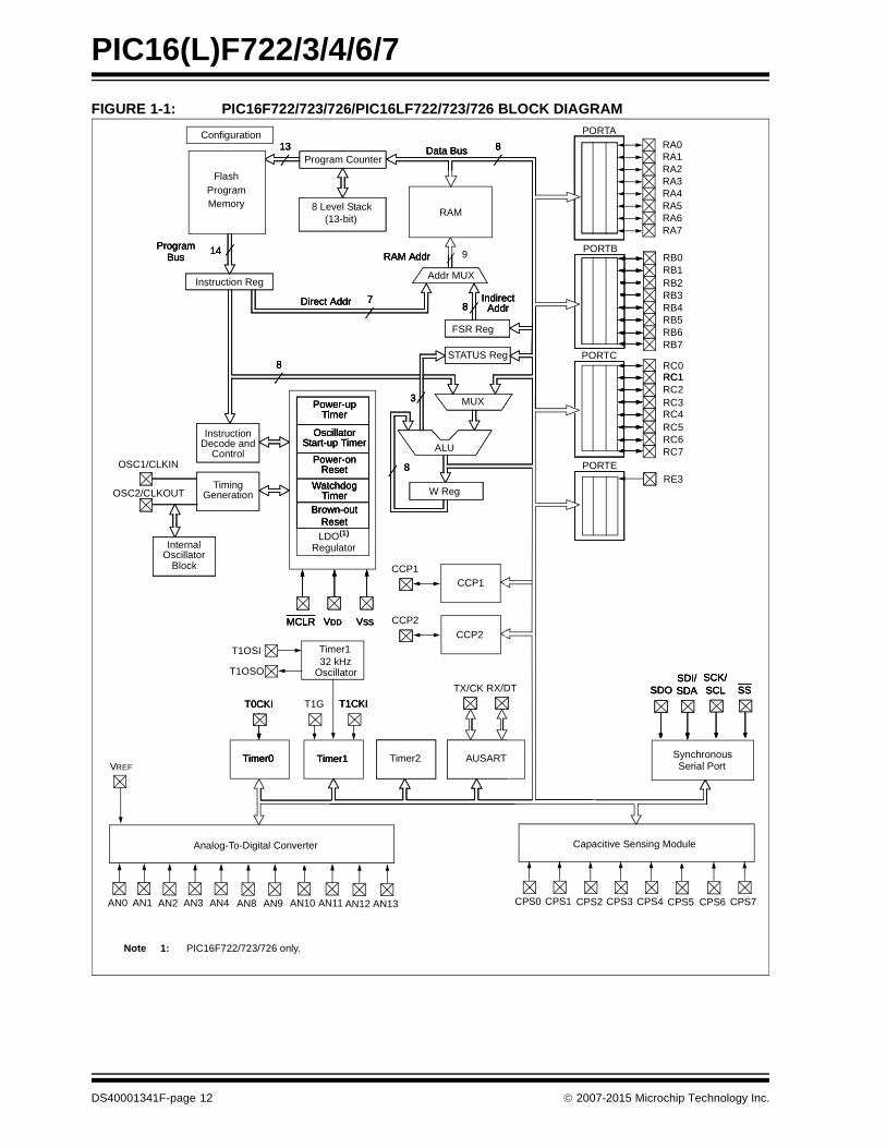
The PIC16(L)F722/3/4/6/7 devices are covered by thisdata sheet. They are available in 28/40/44-pin pack-ages. Figure 1-1 shows a block diagram of thePIC16F722/723/726/PIC16LF722/723/726 devicesand Figure 1-2 shows a block diagram of thePIC16F724/727/PIC16LF724/727 devices. Table 1-1shows the pinout descriptions.
2007-2015 Microchip Technology Inc. DS40001341F-page 11
PIC16(L)F722/3/4/6/7
FIGURE 1-1: PIC16F722/723/726/PIC16LF722/723/726 BLOCK DIAGRAM
13 Data Bus 8
14ProgramBus
Instruction reg
Program Counter
8 Level Stack(13-bit)
Direct Addr 7
RAM Addr 9
Addr MUX
IndirectAddr
FSR reg
STATUS reg
MUX
ALU
W reg
Power-upTimer
OscillatorStart-up Timer
Power-onReset
WatchdogTimer
InstructionDecode &
Control
TimingGeneration
OSC1/CLKIN
OSC2/CLKOUT
MCLR VDD
PORTA
RA4
RC0RC1RC2RC3RC4RC5RC6RC7
8
8
Brown-outReset
AUSARTTimer0 Timer1 Timer2
RA3
RA1RA0
8
3
Analog-To-Digital Converter
RA6RA7
RB6RB7
VSS
T0CKI T1G T1CKI
VREF
Synchronous
SDA SCL SSSDO
Serial Port
SDI/ SCK/TX/CK RX/DT
InternalOscillator
Block
Configuration13 Data Bus 8
14ProgramBus
Instruction reg
Program Counter
8 Level Stack(13-bit)
Direct Addr 7
RAM Addr
Addr MUX
IndirectAddr
FSR reg
STATUS reg
MUX
ALU
W reg
Power-upTimer
OscillatorStart-up Timer
Power-onReset
WatchdogTimer
InstructionDecode &
Control
TimingGeneration
MCLR VDD
RC18
8
Brown-outReset
AUSARTTimer0 Timer1 Timer2
8
3
VSS
T0CKI T1CKI
Synchronous
SDA SCL SSSDO
Serial Port
SDI/ SCK/
InternalOscillator
Block
Configuration13 Data Bus 8
14ProgramBus
Instruction Reg
Program Counter
8 Level Stack(13-bit)
Direct Addr 7
RAM Addr
Addr MUX
IndirectAddr
FSR Reg
STATUS Reg
MUX
ALU
W Reg
Power-upTimer
OscillatorStart-up Timer
Power-onReset
WatchdogTimer
InstructionDecode and
Control
TimingGeneration
MCLR VDD
PORTB
PORTC
RA5
8
8
Brown-outReset
Timer0 Timer1 Timer2
RA2
8
3
RB0RB1RB2RB3RB4RB5
VSS
T0CKI T1CKI
Synchronous
SDA SCL SSSDO
Serial Port
SDI/ SCK/
InternalOscillator
Block
Configuration
CCP2
CCP2
Timer132 kHz
Oscillator
PORTERE3
CCP1CCP1
T1OSI
T1OSO
AN9AN0 AN1 AN2 AN3 AN4 AN8 AN10 AN11 AN12 AN13
LDO(1)
Regulator
FlashProgramMemory
Note 1: PIC16F722/723/726 only.
RAM
Capacitive Sensing Module
CPS6CPS0 CPS1 CPS2 CPS3 CPS4 CPS5 CPS7
DS40001341F-page 12 2007-2015 Microchip Technology Inc.

PIC16(L)F722/3/4/6/7
FIGURE 1-2: PIC16F724/727/PIC16LF724/727 BLOCK DIAGRAM
13 Data Bus 8
14ProgramBus
Instruction reg
Program Counter
8 Level Stack(13-bit)
Direct Addr 7
RAM Addr 9
Addr MUX
IndirectAddr
FSR reg
STATUS reg
MUX
ALU
InstructionDecode &
Control
TimingGeneration
OSC1/CLKIN
OSC2/CLKOUT
PORTA
PORTB
PORTC
PORTD
PORTE
RA4RA5
RC0RC1RC2RC3RC4RC5RC6RC7
RE0
RE1
RE2
8
8
AUSARTTimer0 Timer1 Timer2
RA3
RA1RA0
8
3
RA6RA7
RD0RD1RD2RD3RD4RD5RD6RD7
RB0RB1RB2RB3RB4RB5
RB7
AN6AN0 AN1 AN2 AN3 AN4 AN5 AN7
Synchronous
SDA SCL SSSDO
Serial Port
SDI/ SCK/TX/CK RX/DT
InternalOscillator
Block
Configuration13 Data Bus 8
14ProgramBus
Instruction reg
Program Counter
8 Level Stack(13-bit)
Direct Addr 7
RAM Addr
Addr MUX
IndirectAddr
FSR reg
STATUS reg
MUX
ALU
W Reg
InstructionDecode &
Control
TimingGeneration
PORTB
PORTC
PORTD
PORTE
RC18
8
AUSARTTimer0 Timer1 Timer2
8
3
Synchronous
SDA SCL SSSDO
Serial Port
SDI/ SCK/
InternalOscillator
Block
Configuration13 Data Bus 8
14ProgramBus
Instruction Reg
Program Counter
8 Level Stack(13-bit)
Direct Addr 7
RAM Addr
Addr MUX
IndirectAddr
FSR Reg
STATUS Reg
MUX
ALU
InstructionDecode and
Control
TimingGeneration
PORTB
PORTC
PORTD
PORTE
RC18
8
AUSARTTimer0 Timer1 Timer2
8
3
Analog-To-Digital Converter
RB6
Synchronous
SDA SCL SSSDO
Serial Port
SDI/ SCK/
InternalOscillator
Block
Configuration
RE3CCP2
CCP2
CCP1
CCP1
VREF
RA2
AN9AN8 AN10 AN11 AN12 AN13
Power-upTimer
OscillatorStart-up Timer
Power-onReset
WatchdogTimer
MCLR VDD
Brown-outReset
VSS
T0CKI T1G T1CKI
Power-upTimer
OscillatorStart-up Timer
Power-onReset
WatchdogTimer
MCLR VDD
Brown-outReset
VSS
T0CKI T1CKI
Power-upTimer
OscillatorStart-up Timer
Power-onReset
WatchdogTimer
MCLR VDD
Brown-outReset
VSS
T0CKI T1CKI
Timer132 kHz
Oscillator
T1OSI
T1OSO
LDO(1)
Regulator
Note 1: PIC16F724/727 only.
Capacitive Sensing Module
CPS6CPS0 CPS1 CPS2 CPS3 CPS4 CPS7 CPS8 CPS9 CPS10 CPS11 CPS12 CPS13 CPS14 CPS15CPS5
FlashProgramMemory
RAM
2007-2015 Microchip Technology Inc. DS40001341F-page 13

PIC16(L)F722/3/4/6/7
TABLE 1-1: PIC16(L)F722/3/4/6/7 PINOUT DESCRIPTION
Name FunctionInput Type
Output Type
Description
RA0/AN0/SS/VCAP RA0 TTL CMOS General purpose I/O.
AN0 AN — A/D Channel 0 input.
SS ST — Slave Select input.
VCAP Power Power Filter capacitor for Voltage Regulator (PIC16F72X only).
RA1/AN1 RA1 TTL CMOS General purpose I/O.
AN1 AN — A/D Channel 1 input.
RA2/AN2 RA2 TTL CMOS General purpose I/O.
AN2 AN — A/D Channel 2 input.
RA3/AN3/VREF RA3 TTL CMOS General purpose I/O.
AN3 AN — A/D Channel 3 input.
VREF AN — A/D Voltage Reference input.
RA4/CPS6/T0CKI RA4 TTL CMOS General purpose I/O.
CPS6 AN — Capacitive sensing input 6.
T0CKI ST — Timer0 clock input.
RA5/AN4/CPS7/SS/VCAP RA5 TTL CMOS General purpose I/O.
AN4 AN — A/D Channel 4 input.
CPS7 AN — Capacitive sensing input 7.
SS ST — Slave Select input.
VCAP Power Power Filter capacitor for Voltage Regulator (PIC16F72X only).
RA6/OSC2/CLKOUT/VCAP RA6 TTL CMOS General purpose I/O.
OSC2 — XTAL Crystal/Resonator (LP, XT, HS modes).
CLKOUT — CMOS FOSC/4 output.
VCAP Power Power Filter capacitor for Voltage Regulator (PIC16F72X only).
RA7/OSC1/CLKIN RA7 TTL CMOS General purpose I/O.
OSC1 XTAL — Crystal/Resonator (LP, XT, HS modes).
CLKIN CMOS — External clock input (EC mode).
CLKIN ST — RC oscillator connection (RC mode).
RB0/AN12/CPS0/INT RB0 TTL CMOS General purpose I/O. Individually controlled inter-rupt-on-change. Individually enabled pull-up.
AN12 AN — A/D Channel 12 input.
CPS0 AN — Capacitive sensing input 0.
INT ST — External interrupt.
RB1/AN10/CPS1 RB1 TTL CMOS General purpose I/O. Individually controlled inter-rupt-on-change. Individually enabled pull-up.
AN10 AN — A/D Channel 10 input.
CPS1 AN — Capacitive sensing input 1.
RB2/AN8/CPS2 RB2 TTL CMOS General purpose I/O. Individually controlled inter-rupt-on-change. Individually enabled pull-up.
AN8 AN — A/D Channel 8 input.
CPS2 AN — Capacitive sensing input 2.
RB3/AN9/CPS3/CCP2 RB3 TTL CMOS General purpose I/O. Individually controlled inter-rupt-on-change. Individually enabled pull-up.
AN9 AN — A/D Channel 9 input.
CPS3 AN — Capacitive sensing input 3.
CCP2 ST CMOS Capture/Compare/PWM2.
Legend: AN = Analog input or output CMOS = CMOS compatible input or output OD = Open DrainTTL = TTL compatible input ST = Schmitt Trigger input with CMOS levels I2C = Schmitt Trigger input with I2C HV = High Voltage XTAL = Crystal levels
DS40001341F-page 14 2007-2015 Microchip Technology Inc.

PIC16(L)F722/3/4/6/7
RB4/AN11/CPS4 RB4 TTL CMOS General purpose I/O. Individually controlled inter-rupt-on-change. Individually enabled pull-up.
AN11 AN — A/D Channel 11 input.
CPS4 AN — Capacitive sensing input 4.
RB5/AN13/CPS5/T1G RB5 TTL CMOS General purpose I/O. Individually controlled inter-rupt-on-change. Individually enabled pull-up.
AN13 AN — A/D Channel 13 input.
CPS5 AN — Capacitive sensing input 5.
T1G ST — Timer1 Gate input.
RB6/ICSPCLK/ICDCLK RB6 TTL CMOS General purpose I/O. Individually controlled inter-rupt-on-change. Individually enabled pull-up.
ICSPCLK ST — Serial Programming Clock.
ICDCLK ST — In-Circuit Debug Clock.
RB7/ICSPDAT/ICDDAT RB7 TTL CMOS General purpose I/O. Individually controlled inter-rupt-on-change. Individually enabled pull-up.
ICSPDAT ST CMOS ICSP™ Data I/O.
ICDDAT ST — In-Circuit Data I/O.
RC0/T1OSO/T1CKI RC0 ST CMOS General purpose I/O.
T1OSO XTAL XTAL Timer1 oscillator connection.
T1CKI ST — Timer1 clock input.
RC1/T1OSI/CCP2 RC1 ST CMOS General purpose I/O.
T1OSI XTAL XTAL Timer1 oscillator connection.
CCP2 ST CMOS Capture/Compare/PWM2.
RC2/CCP1 RC2 ST CMOS General purpose I/O.
CCP1 ST CMOS Capture/Compare/PWM1.
RC3/SCK/SCL RC3 ST CMOS General purpose I/O.
SCK ST CMOS SPI clock.
SCL I2C OD I2C clock.
RC4/SDI/SDA RC4 ST CMOS General purpose I/O.
SDI ST — SPI data input.
SDA I2C OD I2C data input/output.
RC5/SDO RC5 ST CMOS General purpose I/O.
SDO — CMOS SPI data output.
RC6/TX/CK RC6 ST CMOS General purpose I/O.
TX — CMOS USART asynchronous transmit.
CK ST CMOS USART synchronous clock.
RC7/RX/DT RC7 ST CMOS General purpose I/O.
RX ST — USART asynchronous input.
DT ST CMOS USART synchronous data.
RD0/CPS8 RD0 ST CMOS General purpose I/O.
CPS8 AN — Capacitive sensing input 8.
RD1/CPS9 RD1 ST CMOS General purpose I/O.
CPS9 AN — Capacitive sensing input 9.
RD2/CPS10 RD2 ST CMOS General purpose I/O.
CPS10 AN — Capacitive sensing input 10.
TABLE 1-1: PIC16(L)F722/3/4/6/7 PINOUT DESCRIPTION (CONTINUED)
Name FunctionInput Type
Output Type
Description
Legend: AN = Analog input or output CMOS = CMOS compatible input or output OD = Open DrainTTL = TTL compatible input ST = Schmitt Trigger input with CMOS levels I2C = Schmitt Trigger input with I2C HV = High Voltage XTAL = Crystal levels
2007-2015 Microchip Technology Inc. DS40001341F-page 15

PIC16(L)F722/3/4/6/7
RD3/CPS11 RD3 ST CMOS General purpose I/O.
CPS11 AN — Capacitive sensing input 11.
RD4/CPS12 RD4 ST CMOS General purpose I/O.
CPS12 AN — Capacitive sensing input 12.
RD5/CPS13 RD5 ST CMOS General purpose I/O.
CPS13 AN — Capacitive sensing input 13.
RD6/CPS14 RD6 ST CMOS General purpose I/O.
CPS14 AN — Capacitive sensing input 14.
RD7/CPS15 RD7 ST CMOS General purpose I/O.
CPS15 AN — Capacitive sensing input 15.
RE0/AN5 RE0 ST CMOS General purpose I/O.
AN5 AN — A/D Channel 5 input.
RE1/AN6 RE1 ST CMOS General purpose I/O.
AN6 AN — A/D Channel 6 input.
RE2/AN7 RE2 ST CMOS General purpose I/O.
AN7 AN — A/D Channel 7 input.
RE3/MCLR/VPP RE3 TTL — General purpose input.
MCLR ST — Master Clear with internal pull-up.
VPP HV — Programming voltage.
VDD VDD Power — Positive supply.
VSS VSS Power — Ground reference.
Note: The PIC16F722/3/4/6/7 devices have an internal low dropout voltage regulator. An external capacitor mustbe connected to one of the available VCAP pins to stabilize the regulator. For more information, seeSection 5.0 “Low Dropout (LDO) Voltage Regulator”. The PIC16LF722/3/4/6/7 devices do not have thevoltage regulator and therefore no external capacitor is required.
TABLE 1-1: PIC16(L)F722/3/4/6/7 PINOUT DESCRIPTION (CONTINUED)
Name FunctionInput Type
Output Type
Description
Legend: AN = Analog input or output CMOS = CMOS compatible input or output OD = Open DrainTTL = TTL compatible input ST = Schmitt Trigger input with CMOS levels I2C = Schmitt Trigger input with I2C HV = High Voltage XTAL = Crystal levels
DS40001341F-page 16 2007-2015 Microchip Technology Inc.

PIC16(L)F722/3/4/6/7
2.0 MEMORY ORGANIZATION
2.1 Program Memory Organization
The PIC16(L)F722/3/4/6/7 has a 13-bit programcounter capable of addressing a 2K x 14 programmemory space for the PIC16F722/LF722(0000h-07FFh), a 4K x 14 program memory space forthe PIC16F723/LF723 and PIC16F724/LF724(0000h-0FFFh) and an 8K x 14 program memory spacefor the PIC16F726/LF726 and PIC16F727/LF727(0000h-1FFFh). Accessing a location above thememory boundaries for the PIC16F722/LF722 willcause a wrap-around within the first 2K x 14 programmemory space. Accessing a location above thememory boundaries for the PIC16F723/LF723 andPIC16F724/LF724 will cause a wrap-around within thefirst 4K x 14 program memory space. The Reset vectoris at 0000h and the interrupt vector is at 0004h.
FIGURE 2-1: PROGRAM MEMORY MAP AND STACK FOR THE PIC16F722/LF722
FIGURE 2-2: PROGRAM MEMORY MAP AND STACK FOR THE PIC16F723/LF723 AND PIC16F724/LF724
PC<12:0>
13
0000h
0004h
Stack Level 1
Stack Level 8
Reset Vector
Interrupt Vector
CALL, RETURNRETFIE, RETLW
Stack Level 2
0005hOn-chipProgramMemory
Page 007FFh
Wraps to Page 0
Wraps to Page 0
Wraps to Page 0
0800h
0FFFh1000h
17FFh1800h
1FFFh
PC<12:0>
13
0000h
0004h
Stack Level 1
Stack Level 8
Reset Vector
Interrupt Vector
CALL, RETURNRETFIE, RETLW
Stack Level 2
0005h
On-chipProgramMemory
Page 0
Page 1
07FFh0800h
0FFFh
Wraps to Page 0
Wraps to Page 1
1000h
17FFh1800h
1FFFh
2007-2015 Microchip Technology Inc. DS40001341F-page 17

PIC16(L)F722/3/4/6/7
FIGURE 2-3: PROGRAM MEMORY MAP AND STACK FOR THE PIC16F726/LF726 AND PIC16F727/LF727
2.2 Data Memory Organization
The data memory is partitioned into multiple bankswhich contain the General Purpose Registers (GPRs)and the Special Function Registers (SFRs). Bits RP0and RP1 are bank select bits.
RP1 RP0
0 0 Bank 0 is selected
0 1 Bank 1 is selected
1 0 Bank 2 is selected
1 1 Bank 3 is selected
Each bank extends up to 7Fh (128 bytes). The lowerlocations of each bank are reserved for the SpecialFunction Registers. Above the Special FunctionRegisters are the General Purpose Registers,implemented as static RAM. All implemented bankscontain Special Function Registers. Some frequentlyused Special Function Registers from one bank aremirrored in another bank for code reduction andquicker access.
2.2.1 GENERAL PURPOSE REGISTER FILE
The register file is organized as 128 x 8 bits in thePIC16F722/LF722, 192 x 8 bits in the PIC16F723/LF723and PIC16F724/LF724, and 368 x 8 bits in thePIC16F726/LF726 and PIC16F727/LF727. Eachregister is accessed either directly or indirectly throughthe File Select Register (FSR), (Refer to Section 2.5“Indirect Addressing, INDF and FSR Registers”).
2.2.2 SPECIAL FUNCTION REGISTERS
The Special Function Registers are registers used bythe CPU and peripheral functions for controlling thedesired operation of the device (refer to Table 2-1).These registers are static RAM.
The Special Function Registers can be classified intotwo sets: core and peripheral. The Special FunctionRegisters associated with the “core” are described inthis section. Those related to the operation of theperipheral features are described in the section of thatperipheral feature.
PC<12:0>
13
0000h
0004h
Stack Level 1
Stack Level 8
Reset Vector
Interrupt Vector
CALL, RETURNRETFIE, RETLW
Stack Level 2
0005h
On-chip
1FFFh
ProgramMemory
Page 0
Page 1
07FFh0800h
0FFFh1000h
Page 2
Page 3
17FFh1800h
DS40001341F-page 18 2007-2015 Microchip Technology Inc.

PIC16(L)F722/3/4/6/7
FIGURE 2-4: PIC16F722/LF722 SPECIAL FUNCTION REGISTERS
File Address
Indirect addr.(*) 00h Indirect addr.(*) 80h Indirect addr.(*) 100h Indirect addr.(*) 180h
TMR0 01h OPTION 81h TMR0 101h OPTION 181h
PCL 02h PCL 82h PCL 102h PCL 182h
STATUS 03h STATUS 83h STATUS 103h STATUS 183h
FSR 04h FSR 84h FSR 104h FSR 184h
PORTA 05h TRISA 85h 105h ANSELA 185h
PORTB 06h TRISB 86h 106h ANSELB 186h
PORTC 07h TRISC 87h 107h 187h
08h 88h CPSCON0 108h 188h
PORTE 09h TRISE 89h CPSCON1 109h 189h
PCLATH 0Ah PCLATH 8Ah PCLATH 10Ah PCLATH 18Ah
INTCON 0Bh INTCON 8Bh INTCON 10Bh INTCON 18Bh
PIR1 0Ch PIE1 8Ch PMDATL 10Ch PMCON1 18Ch
PIR2 0Dh PIE2 8Dh PMADRL 10Dh Reserved 18Dh
TMR1L 0Eh PCON 8Eh PMDATH 10Eh Reserved 18Eh
TMR1H 0Fh T1GCON 8Fh PMADRH 10Fh Reserved 18Fh
T1CON 10h OSCCON 90h 110h 190h
TMR2 11h OSCTUNE 91h 111h 191h
T2CON 12h PR2 92h 112h 192h
SSPBUF 13h SSPADD/SSPMSK 93h 113h 193h
SSPCON 14h SSPSTAT 94h 114h 194h
CCPR1L 15h WPUB 95h 115h 195h
CCPR1H 16h IOCB 96h 116h 196h
CCP1CON 17h 97h 117h 197h
RCSTA 18h TXSTA 98h 118h 198h
TXREG 19h SPBRG 99h 119h 199h
RCREG 1Ah 9Ah 11Ah 19Ah
CCPR2L 1Bh 9Bh 11Bh 19Bh
CCPR2H 1Ch APFCON 9Ch 11Ch 19Ch
CCP2CON 1Dh FVRCON 9Dh 11Dh 19Dh
ADRES 1Eh 9Eh 11Eh 19Eh
ADCON0 1Fh ADCON1 9Fh 11Fh 19Fh
GeneralPurposeRegister96 Bytes
20h
GeneralPurposeRegister32 Bytes
A0h
BFh
120h 1A0h
C0h
EFh 16Fh 1EFh
Accesses70h-7Fh
F0h
Accesses70h-7Fh
170h
Accesses70h-7Fh
1F0h
7Fh FFh 17Fh 1FFh
Bank 0 Bank 1 Bank 2 Bank 3
Legend: = Unimplemented data memory locations, read as ‘0’.* = Not a physical register.
2007-2015 Microchip Technology Inc. DS40001341F-page 19

PIC16(L)F722/3/4/6/7
FIGURE 2-5: PIC16F723/LF723 AND PIC16F724/LF724 SPECIAL FUNCTION REGISTERS
Legend: = Unimplemented data memory locations, read as ‘0’.* = Not a physical register.
Note 1: PORTD, TRISD, ANSELD and ANSELE are not implemented on the PIC16F723/LF723, read as ‘0’
File Address
Indirect addr.(*) 00h Indirect addr.(*) 80h Indirect addr.(*) 100h Indirect addr.(*) 180h
TMR0 01h OPTION 81h TMR0 101h OPTION 181h
PCL 02h PCL 82h PCL 102h PCL 182h
STATUS 03h STATUS 83h STATUS 103h STATUS 183h
FSR 04h FSR 84h FSR 104h FSR 184h
PORTA 05h TRISA 85h 105h ANSELA 185h
PORTB 06h TRISB 86h 106h ANSELB 186h
PORTC 07h TRISC 87h 107h 187h
PORTD(1) 08h TRISD(1) 88h CPSCON0 108h ANSELD(1)188h
PORTE 09h TRISE 89h CPSCON1 109h ANSELE(1)189h
PCLATH 0Ah PCLATH 8Ah PCLATH 10Ah PCLATH 18Ah
INTCON 0Bh INTCON 8Bh INTCON 10Bh INTCON 18Bh
PIR1 0Ch PIE1 8Ch PMDATL 10Ch PMCON1 18Ch
PIR2 0Dh PIE2 8Dh PMADRL 10Dh Reserved 18Dh
TMR1L 0Eh PCON 8Eh PMDATH 10Eh Reserved 18Eh
TMR1H 0Fh T1GCON 8Fh PMADRH 10Fh Reserved 18Fh
T1CON 10h OSCCON 90h 110h 190h
TMR2 11h OSCTUNE 91h 111h 191h
T2CON 12h PR2 92h 112h 192h
SSPBUF 13h SSPADD/SSPMSK 93h 113h 193h
SSPCON 14h SSPSTAT 94h 114h 194h
CCPR1L 15h WPUB 95h 115h 195h
CCPR1H 16h IOCB 96h 116h 196h
CCP1CON 17h 97h 117h 197h
RCSTA 18h TXSTA 98h 118h 198h
TXREG 19h SPBRG 99h 119h 199h
RCREG 1Ah 9Ah 11Ah 19Ah
CCPR2L 1Bh 9Bh 11Bh 19Bh
CCPR2H 1Ch APFCON 9Ch 11Ch 19Ch
CCP2CON 1Dh FVRCON 9Dh 11Dh 19Dh
ADRES 1Eh 9Eh 11Eh 19Eh
ADCON0 1Fh ADCON1 9Fh 11Fh 19Fh
GeneralPurposeRegister96 Bytes
20h
7Fh
GeneralPurposeRegister80 Bytes
A0h
EFh
General PurposeRegister16 Bytes
120h
12Fh130h
16Fh
1A0h
1EFh
Accesses70h-7Fh
F0h
FFh
Accesses70h-7Fh
170h
17Fh
Accesses70h-7Fh
1F0h
1FFh
Bank 0 Bank 1 Bank 2 Bank 3
DS40001341F-page 20 2007-2015 Microchip Technology Inc.

PIC16(L)F722/3/4/6/7
FIGURE 2-6: PIC16F726/LF726 AND PIC16F727/LF727 SPECIAL FUNCTION REGISTERS
Legend: = Unimplemented data memory locations, read as ‘0’, * = Not a physical register
Note 1: PORTD, TRISD, ANSELD and ANSELE are not implemented on the PIC16F726/LF726, read as ‘0’
File Address
Indirect addr.(*) 00h Indirect addr.(*) 80h Indirect addr.(*) 100h Indirect addr.(*) 180h
TMR0 01h OPTION 81h TMR0 101h OPTION 181h
PCL 02h PCL 82h PCL 102h PCL 182h
STATUS 03h STATUS 83h STATUS 103h STATUS 183h
FSR 04h FSR 84h FSR 104h FSR 184h
PORTA 05h TRISA 85h 105h ANSELA 185h
PORTB 06h TRISB 86h 106h ANSELB 186h
PORTC 07h TRISC 87h 107h 187h
PORTD(1) 08h TRISD(1) 88h CPSCON0 108h ANSELD(1)188h
PORTE 09h TRISE 89h CPSCON1 109h ANSELE(1)189h
PCLATH 0Ah PCLATH 8Ah PCLATH 10Ah PCLATH 18Ah
INTCON 0Bh INTCON 8Bh INTCON 10Bh INTCON 18Bh
PIR1 0Ch PIE1 8Ch PMDATL 10Ch PMCON1 18Ch
PIR2 0Dh PIE2 8Dh PMADRL 10Dh Reserved 18Dh
TMR1L 0Eh PCON 8Eh PMDATH 10Eh Reserved 18Eh
TMR1H 0Fh T1GCON 8Fh PMADRH 10Fh Reserved 18Fh
T1CON 10h OSCCON 90h
GeneralPurposeRegister16 Bytes
110h
GeneralPurposeRegister16 Bytes
190h
TMR2 11h OSCTUNE 91h 111h 191h
T2CON 12h PR2 92h 112h 192h
SSPBUF 13h SSPADD/SSPMSK 93h 113h 193h
SSPCON 14h SSPSTAT 94h 114h 194h
CCPR1L 15h WPUB 95h 115h 195h
CCPR1H 16h IOCB 96h 116h 196h
CCP1CON 17h 97h 117h 197h
RCSTA 18h TXSTA 98h 118h 198h
TXREG 19h SPBRG 99h 119h 199h
RCREG 1Ah 9Ah 11Ah 19Ah
CCPR2L 1Bh 9Bh 11Bh 19Bh
CCPR2H 1Ch APFCON 9Ch 11Ch 19Ch
CCP2CON 1Dh FVRCON 9Dh 11Dh 19Dh
ADRES 1Eh 9Eh 11Eh 19Eh
ADCON0 1Fh ADCON1 9Fh 11Fh 19Fh
GeneralPurposeRegister96 Bytes
20h
7Fh
GeneralPurposeRegister80 Bytes
A0h
EFh
GeneralPurposeRegister80 Bytes
120h
16Fh
GeneralPurposeRegister80 Bytes
1A0h
1EFh
Accesses70h-7Fh
F0h
FFh
Accesses70h-7Fh
170h
17Fh
Accesses70h-7Fh
1F0h
1FFh
Bank 0 Bank 1 Bank 2 Bank 3
2007-2015 Microchip Technology Inc. DS40001341F-page 21

PIC16(L)F722/3/4/6/7
TABLE 2-1: PIC16(L)F722/3/4/6/7 SPECIAL FUNCTION REGISTER SUMMARY
Address Name Bit 7 Bit 6 Bit 5 Bit 4 Bit 3 Bit 2 Bit 1 Bit 0Value on:POR, BOR
Page
Bank 0
00h(2) INDF Addressing this location uses contents of FSR to address data memory (not a physical register) xxxx xxxx 29,37
01h TMR0 Timer0 Module Register xxxx xxxx 105,37
02h(2) PCL Program Counter (PC) Least Significant Byte 0000 0000 28,37
03h(2) STATUS IRP RP1 RP0 TO PD Z DC C 0001 1xxx 25,37
04h(2) FSR Indirect Data Memory Address Pointer xxxx xxxx 29,37
05h PORTA RA7 RA6 RA5 RA4 RA3 RA2 RA1 RA0 xxxx xxxx 51,37
06h PORTB RB7 RB6 RB5 RB4 RB3 RB2 RB1 RB0 xxxx xxxx 60,37
07h PORTC RC7 RC6 RC5 RC4 RC3 RC2 RC1 RC0 xxxx xxxx 70,37
08h(3) PORTD RD7 RD6 RD5 RD4 RD3 RD2 RD1 RD0 xxxx xxxx 77,37
09h PORTE — — — — RE3 RE2(3) RE1(3) RE0(3) ---- xxxx 81,37
0Ah(1, 2) PCLATH — — — Write Buffer for the upper 5 bits of the Program Counter ---0 0000 28,37
0Bh(2) INTCON GIE PEIE T0IE INTE RBIE T0IF INTF RBIF 0000 000x 44,37
0Ch PIR1 TMR1GIF ADIF RCIF TXIF SSPIF CCP1IF TMR2IF TMR1IF 0000 0000 47,37
0Dh PIR2 — — — — — — — CCP2IF ---- ---0 48,37
0Eh TMR1L Holding Register for the Least Significant Byte of the 16-bit TMR1 Register xxxx xxxx 113,37
0Fh TMR1H Holding Register for the Most Significant Byte of the 16-bit TMR1 Register xxxx xxxx 113,37
10h T1CON TMR1CS1 TMR1CS0 T1CKPS1 T1CKPS0 T1OSCEN T1SYNC — TMR1ON 0000 00-0 117,37
11h TMR2 Timer2 Module Register 0000 0000 120,37
12h T2CON — TOUTPS3 TOUTPS2 TOUTPS1 TOUTPS0 TMR2ON T2CKPS1 T2CKPS0 -000 0000 121,37
13h SSPBUF Synchronous Serial Port Receive Buffer/Transmit Register xxxx xxxx 161,37
14h SSPCON WCOL SSPOV SSPEN CKP SSPM3 SSPM2 SSPM1 SSPM0 0000 0000 178,37
15h CCPR1L Capture/Compare/PWM Register (LSB) xxxx xxxx 130,37
16h CCPR1H Capture/Compare/PWM Register (MSB) xxxx xxxx 130,37
17h CCP1CON — — DC1B1 DC1B0 CCP1M3 CCP1M2 CCP1M1 CCP1M0 --00 0000 129,37
18h RCSTA SPEN RX9 SREN CREN ADDEN FERR OERR RX9D 0000 000x 148,37
19h TXREG USART Transmit Data Register 0000 0000 147,37
1Ah RCREG USART Receive Data Register 0000 0000 145,37
1Bh CCPR2L Capture/Compare/PWM Register 2 (LSB) xxxx xxxx 130,37
1Ch CCPR2H Capture/Compare/PWM Register 2 (MSB) xxxx xxxx 130,37
1Dh CCP2CON — — DC2B1 DC2B0 CCP2M3 CCP2M2 CCP2M1 CCP2M0 --00 0000 129,37
1Eh ADRES A/D Result Register xxxx xxxx 100,37
1Fh ADCON0 — — CHS3 CHS2 CHS1 CHS0 GO/DONE ADON --00 0000 99,37
Legend: x = unknown, u = unchanged, q = value depends on condition, - = unimplemented, read as ‘0’, r = reserved. Shaded locations are unimplemented, read as ‘0’.
Note 1: The upper byte of the program counter is not directly accessible. PCLATH is a holding register for the PC<12:8>, whose contents are transferred to the upper byte of the program counter.
2: These registers can be addressed from any bank.3: These registers/bits are not implemented on PIC16F722/723/726/PIC16LF722/723/726 devices, read as ‘0’.4: Accessible only when SSPM<3:0> = 1001.5: Accessible only when SSPM<3:0> 1001.6: This bit is always ‘1’ as RE3 is input-only.
DS40001341F-page 22 2007-2015 Microchip Technology Inc.

PIC16(L)F722/3/4/6/7
Bank 1
80h(2) INDF Addressing this location uses contents of FSR to address data memory (not a physical register) xxxx xxxx 29,37
81h OPTION_REG RBPU INTEDG T0CS T0SE PSA PS2 PS1 PS0 1111 1111 26,37
82h(2) PCL Program Counter (PC) Least Significant Byte 0000 0000 28,37
83h(2) STATUS IRP RP1 RP0 TO PD Z DC C 0001 1xxx 25,37
84h(2) FSR Indirect Data Memory Address Pointer xxxx xxxx 29,37
85h TRISA TRISA7 TRISA6 TRISA5 TRISA4 TRISA3 TRISA2 TRISA1 TRISA0 1111 1111 51,37
86h TRISB TRISB7 TRISB6 TRISB5 TRISB4 TRISB3 TRISB2 TRISB1 TRISB0 1111 1111 60,37
87h TRISC TRISC7 TRISC6 TRISC5 TRISC4 TRISC3 TRISC2 TRISC1 TRISC0 1111 1111 70,37
88h(3) TRISD TRISD7 TRISD6 TRISD5 TRISD4 TRISD3 TRISD2 TRISD1 TRISD0 1111 1111 78,37
89h TRISE — — — — TRISE3(6) TRISE2(3) TRISE1(3) TRISE0(3) ---- 1111 81,37
8Ah(1, 2) PCLATH — — — Write Buffer for the upper 5 bits of the Program Counter ---0 0000 28,37
8Bh(2) INTCON GIE PEIE T0IE INTE RBIE T0IF INTF RBIF 0000 000x 44,37
8Ch PIE1 TMR1GIE ADIE RCIE TXIE SSPIE CCP1IE TMR2IE TMR1IE 0000 0000 45,37
8Dh PIE2 — — — — — — — CCP2IE ---- ---0 46,37
8Eh PCON — — — — — — POR BOR ---- --qq 27,38
8Fh T1GCON TMR1GE T1GPOL T1GTM T1GSPM T1GGO/DONE
T1GVAL T1GSS1 T1GSS0 0000 0x00 118,38
90h OSCCON — — IRCF1 IRCF0 ICSL ICSS — — --10 qq-- 87,38
91h OSCTUNE — — TUN5 TUN4 TUN3 TUN2 TUN1 TUN0 --00 0000 88,38
92h PR2 Timer2 Period Register 1111 1111 120,38
93h SSPADD(5) Synchronous Serial Port (I2C mode) Address Register 0000 0000 169,38
93h SSPMSK(4) Synchronous Serial Port (I2C mode) Address Mask Register 1111 1111 180,38
94h SSPSTAT SMP CKE D/A P S R/W UA BF 0000 0000 179,38
95h WPUB WPUB7 WPUB6 WPUB5 WPUB4 WPUB3 WPUB2 WPUB1 WPUB0 1111 1111 61,38
96h IOCB IOCB7 IOCB6 IOCB5 IOCB4 IOCB3 IOCB2 IOCB1 IOCB0 0000 0000 61,38
97h — Unimplemented — —
98h TXSTA CSRC TX9 TXEN SYNC — BRGH TRMT TX9D 0000 -010 147,38
99h SPBRG BRG7 BRG6 BRG5 BRG4 BRG3 BRG2 BRG1 BRG0 0000 0000 149,38
9Ah — Unimplemented — —
9Bh — Unimplemented — —
9Ch APFCON — — — — — — SSSEL CCP2SEL ---- --00 50,38
9Dh FVRCON FVRRDY FVREN — — — — ADFVR1 ADFVR0 q0-- --00 104,38
9Eh — Unimplemented — —
9Fh ADCON1 — ADCS2 ADCS1 ADCS0 — — ADREF1 ADREF0 0000 --00 100,38
TABLE 2-1: PIC16(L)F722/3/4/6/7 SPECIAL FUNCTION REGISTER SUMMARY (CONTINUED)
Address Name Bit 7 Bit 6 Bit 5 Bit 4 Bit 3 Bit 2 Bit 1 Bit 0Value on:POR, BOR
Page
Legend: x = unknown, u = unchanged, q = value depends on condition, - = unimplemented, read as ‘0’, r = reserved. Shaded locations are unimplemented, read as ‘0’.
Note 1: The upper byte of the program counter is not directly accessible. PCLATH is a holding register for the PC<12:8>, whose contents are transferred to the upper byte of the program counter.
2: These registers can be addressed from any bank.3: These registers/bits are not implemented on PIC16F722/723/726/PIC16LF722/723/726 devices, read as ‘0’.4: Accessible only when SSPM<3:0> = 1001.5: Accessible only when SSPM<3:0> 1001.6: This bit is always ‘1’ as RE3 is input-only.
2007-2015 Microchip Technology Inc. DS40001341F-page 23

PIC16(L)F722/3/4/6/7
Bank 2
100h(2) INDF Addressing this location uses contents of FSR to address data memory (not a physical register) xxxx xxxx 29,37
101h TMR0 Timer0 Module Register xxxx xxxx 105,37
102h(2) PCL Program Counter’s (PC) Least Significant Byte 0000 0000 28,37
103h(2) STATUS IRP RP1 RP0 TO PD Z DC C 0001 1xxx 25,37
104h(2) FSR Indirect Data Memory Address Pointer xxxx xxxx 29,37
105h — Unimplemented — —
106h — Unimplemented — —
107h — Unimplemented — —
108h CPSCON0 CPSON — — — CPSRNG1 CPSRNG0 CPSOUT T0XCS 0--- 0000 126,38
109h CPSCON1 — — — — CPSCH3 CPSCH2 CPSCH1 CPSCH0 ---- 0000 127,38
10Ah(1, 2) PCLATH — — — Write Buffer for the upper 5 bits of the Program Counter ---0 0000 28,37
10Bh(2) INTCON GIE PEIE T0IE INTE RBIE T0IF INTF RBIF 0000 000x 44,37
10Ch PMDATL Program Memory Read Data Register Low Byte xxxx xxxx 181,38
10Dh PMADRL Program Memory Read Address Register Low Byte xxxx xxxx 181,38
10Eh PMDATH — — Program Memory Read Data Register High Byte --xx xxxx 181,38
10Fh PMADRH — — — Program Memory Read Address Register High Byte ---x xxxx 181,38
Bank 3
180h(2) INDF Addressing this location uses contents of FSR to address data memory (not a physical register) xxxx xxxx 29,37
181h OPTION_REG RBPU INTEDG T0CS T0SE PSA PS2 PS1 PS0 1111 1111 26,37
182h(2) PCL Program Counter (PC) Least Significant Byte 0000 0000 28,37
183h(2) STATUS IRP RP1 RP0 TO PD Z DC C 0001 1xxx 25,37
184h(2) FSR Indirect Data Memory Address Pointer xxxx xxxx 29,37
185h ANSELA — — ANSA5 ANSA4 ANSA3 ANSA2 ANSA1 ANSA0 --11 1111 52,38
186h ANSELB — — ANSB5 ANSB4 ANSB3 ANSB2 ANSB1 ANSB0 --11 1111 61,38
187h — Unimplemented — —
188h ANSELD ANSD7 ANSD6 ANSD5 ANSD4 ANSD3 ANSD2 ANSD1 ANSD0 1111 1111 78,38
189h(3) ANSELE — — — — — ANSE2 ANSE1 ANSE0 ---- -111 82,38
18Ah(1, 2) PCLATH — — — Write Buffer for the upper 5 bits of the Program Counter ---0 0000 28,37
18Bh(2) INTCON GIE PEIE T0IE INTE RBIE T0IF INTF RBIF 0000 000x 44,37
18Ch PMCON1 Reserved — — — — — — RD 1--- ---0 182,38
18Dh — Unimplemented — —
18Eh — Unimplemented — —
18Fh — Unimplemented — —
TABLE 2-1: PIC16(L)F722/3/4/6/7 SPECIAL FUNCTION REGISTER SUMMARY (CONTINUED)
Address Name Bit 7 Bit 6 Bit 5 Bit 4 Bit 3 Bit 2 Bit 1 Bit 0Value on:POR, BOR
Page
Legend: x = unknown, u = unchanged, q = value depends on condition, - = unimplemented, read as ‘0’, r = reserved. Shaded locations are unimplemented, read as ‘0’.
Note 1: The upper byte of the program counter is not directly accessible. PCLATH is a holding register for the PC<12:8>, whose contents are transferred to the upper byte of the program counter.
2: These registers can be addressed from any bank.3: These registers/bits are not implemented on PIC16F722/723/726/PIC16LF722/723/726 devices, read as ‘0’.4: Accessible only when SSPM<3:0> = 1001.5: Accessible only when SSPM<3:0> 1001.6: This bit is always ‘1’ as RE3 is input-only.
DS40001341F-page 24 2007-2015 Microchip Technology Inc.

PIC16(L)F722/3/4/6/7
2.2.2.1 STATUS Register
The STATUS register, shown in Register 2-1, contains:
• the arithmetic status of the ALU
• the Reset status
• the bank select bits for data memory (SRAM)
The STATUS register can be the destination for anyinstruction, like any other register. If the STATUSregister is the destination for an instruction that affectsthe Z, DC or C bits, then the write to these three bits isdisabled. These bits are set or cleared according to thedevice logic. Furthermore, the TO and PD bits are notwritable. Therefore, the result of an instruction with theSTATUS register as destination may be different thanintended.
For example, CLRF STATUS will clear the upper threebits and set the Z bit. This leaves the STATUS registeras ‘000u u1uu’ (where u = unchanged).
It is recommended, therefore, that only BCF, BSF,SWAPF and MOVWF instructions are used to alter theSTATUS register, because these instructions do notaffect any Status bits. For other instructions notaffecting any Status bits (Refer to Section 21.0“Instruction Set Summary”).
Note 1: The C and DC bits operate as Borrowand Digit Borrow out bits, respectively, insubtraction.
REGISTER 2-1: STATUS: STATUS REGISTER
R/W-0 R/W-0 R/W-0 R-1 R-1 R/W-x R/W-x R/W-x
IRP RP1 RP0 TO PD Z DC(1) C(1)
bit 7 bit 0
Legend:
R = Readable bit W = Writable bit U = Unimplemented bit, read as ‘0’
-n = Value at POR ‘1’ = Bit is set ‘0’ = Bit is cleared x = Bit is unknown
bit 7 IRP: Register Bank Select bit (used for indirect addressing)
1 = Bank 2, 3 (100h-1FFh)0 = Bank 0, 1 (00h-FFh)
bit 6-5 RP<1:0>: Register Bank Select bits (used for direct addressing)
00 = Bank 0 (00h-7Fh)01 = Bank 1 (80h-FFh)10 = Bank 2 (100h-17Fh)11 = Bank 3 (180h-1FFh)
bit 4 TO: Time-out bit
1 = After power-up, CLRWDT instruction or SLEEP instruction0 = A WDT time out occurred
bit 3 PD: Power-down bit
1 = After power-up or by the CLRWDT instruction0 = By execution of the SLEEP instruction
bit 2 Z: Zero bit
1 = The result of an arithmetic or logic operation is zero0 = The result of an arithmetic or logic operation is not zero
bit 1 DC: Digit Carry/Digit Borrow bit (ADDWF, ADDLW,SUBLW,SUBWF instructions)(1)
1 = A carry out from the 4th low-order bit of the result occurred0 = No carry-out from the 4th low-order bit of the result
bit 0 C: Carry/Borrow bit(1) (ADDWF, ADDLW, SUBLW, SUBWF instructions)(1)
1 = A carry out from the Most Significant bit of the result occurred0 = No carry out from the Most Significant bit of the result occurred
Note 1: For Borrow, the polarity is reversed. A subtraction is executed by adding the two’s complement of the second operand. For rotate (RRF, RLF) instructions, this bit is loaded with either the high-order or low-order bit of the source register.
2007-2015 Microchip Technology Inc. DS40001341F-page 25
PIC16(L)F722/3/4/6/7
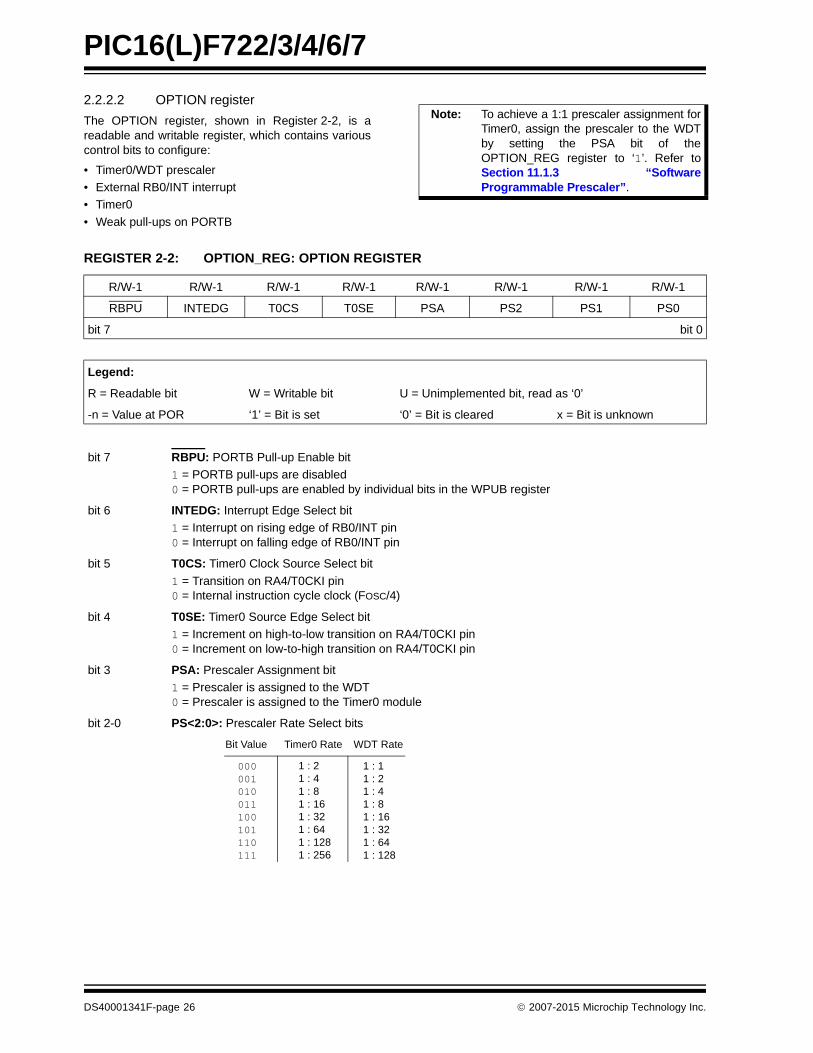
2.2.2.2 OPTION register
The OPTION register, shown in Register 2-2, is areadable and writable register, which contains variouscontrol bits to configure:
• Timer0/WDT prescaler
• External RB0/INT interrupt
• Timer0
• Weak pull-ups on PORTB
Note: To achieve a 1:1 prescaler assignment forTimer0, assign the prescaler to the WDTby setting the PSA bit of theOPTION_REG register to ‘1’. Refer toSection 11.1.3 “SoftwareProgrammable Prescaler”.
REGISTER 2-2: OPTION_REG: OPTION REGISTER
R/W-1 R/W-1 R/W-1 R/W-1 R/W-1 R/W-1 R/W-1 R/W-1
RBPU INTEDG T0CS T0SE PSA PS2 PS1 PS0
bit 7 bit 0
Legend:
R = Readable bit W = Writable bit U = Unimplemented bit, read as ‘0’
-n = Value at POR ‘1’ = Bit is set ‘0’ = Bit is cleared x = Bit is unknown
bit 7 RBPU: PORTB Pull-up Enable bit
1 = PORTB pull-ups are disabled0 = PORTB pull-ups are enabled by individual bits in the WPUB register
bit 6 INTEDG: Interrupt Edge Select bit
1 = Interrupt on rising edge of RB0/INT pin0 = Interrupt on falling edge of RB0/INT pin
bit 5 T0CS: Timer0 Clock Source Select bit
1 = Transition on RA4/T0CKI pin0 = Internal instruction cycle clock (FOSC/4)
bit 4 T0SE: Timer0 Source Edge Select bit
1 = Increment on high-to-low transition on RA4/T0CKI pin0 = Increment on low-to-high transition on RA4/T0CKI pin
bit 3 PSA: Prescaler Assignment bit
1 = Prescaler is assigned to the WDT0 = Prescaler is assigned to the Timer0 module
bit 2-0 PS<2:0>: Prescaler Rate Select bits
000001010011100101110111
1 : 21 : 41 : 81 : 161 : 321 : 641 : 1281 : 256
1 : 11 : 21 : 41 : 81 : 161 : 321 : 641 : 128
Bit Value Timer0 Rate WDT Rate
DS40001341F-page 26 2007-2015 Microchip Technology Inc.

PIC16(L)F722/3/4/6/7
2.2.2.3 PCON Register
The Power Control (PCON) register contains flag bits(refer to Table 3-2) to differentiate between a:
• Power-on Reset (POR)
• Brown-out Reset (BOR)
• Watchdog Timer Reset (WDT)
• External MCLR Reset
The PCON register also controls the software enable ofthe BOR.
The PCON register bits are shown in Register 2-3.
REGISTER 2-3: PCON: POWER CONTROL REGISTER
U-0 U-0 U-0 U-0 U-0 U-0 R/W-q R/W-q
— — — — — — POR BOR
bit 7 bit 0
Legend:
R = Readable bit W = Writable bit U = Unimplemented bit, read as ‘0’
-n = Value at POR ‘1’ = Bit is set ‘0’ = Bit is cleared x = Bit is unknown
q = Value depends on condition
bit 7-2 Unimplemented: Read as ‘0’
bit 1 POR: Power-on Reset Status bit
1 = No Power-on Reset occurred0 = A Power-on Reset occurred (must be set in software after a Power-on Reset occurs)
bit 0 BOR: Brown-out Reset Status bit
1 = No Brown-out Reset occurred0 = A Brown-out Reset occurred (must be set in software after a Power-on Reset or Brown-out Reset
occurs)
Note 1: Set BOREN<1:0> = 01 in the Configuration Word register for this bit to control the BOR.
2007-2015 Microchip Technology Inc. DS40001341F-page 27

PIC16(L)F722/3/4/6/7
2.3 PCL and PCLATH
The Program Counter (PC) is 13 bits wide. The lowbyte comes from the PCL register, which is a readableand writable register. The high byte (PC<12:8>) is notdirectly readable or writable and comes fromPCLATH. On any Reset, the PC is cleared. Figure 2-7shows the two situations for the loading of the PC. Theupper example in Figure 2-7 shows how the PC isloaded on a write to PCL (PCLATH<4:0> PCH).The lower example in Figure 2-7 shows how the PC isloaded during a CALL or GOTO instruction(PCLATH<4:3> PCH).
FIGURE 2-7: LOADING OF PC IN DIFFERENT SITUATIONS
2.3.1 COMPUTED GOTO
A computed GOTO is accomplished by adding an offsetto the program counter (ADDWF PCL). When perform-ing a table read using a computed GOTO method, careshould be exercised if the table location crosses a PCLmemory boundary (each 256-byte block). Refer to theApplication Note AN556, Implementing a Table Read(DS00556).
2.3.2 STACK
All devices have an 8-level x 13-bit wide hardwarestack (refer to Figures 2-1 and 2-3). The stack space isnot part of either program or data space and the StackPointer is not readable or writable. The PC is PUSHedonto the stack when a CALL instruction is executed oran interrupt causes a branch. The stack is POPed inthe event of a RETURN, RETLW or a RETFIE instructionexecution. PCLATH is not affected by a PUSH or POPoperation.
The stack operates as a circular buffer. This means thatafter the stack has been PUSHed eight times, the ninthPUSH overwrites the value that was stored from thefirst PUSH. The tenth PUSH overwrites the secondPUSH (and so on).
2.4 Program Memory Paging
All devices are capable of addressing a continuous 8Kword block of program memory. The CALL and GOTOinstructions provide only 11 bits of address to allowbranching within any 2K program memory page. Whendoing a CALL or GOTO instruction, the upper two bits ofthe address are provided by PCLATH<4:3>. Whendoing a CALL or GOTO instruction, the user must ensurethat the page select bits are programmed so that thedesired program memory page is addressed. If a returnfrom a CALL instruction (or interrupt) is executed, theentire 13-bit PC is POPed off the stack. Therefore,manipulation of the PCLATH<4:3> bits is not requiredfor the RETURN instructions (which POPs the addressfrom the stack).
Example 2-1 shows the calling of a subroutine inpage 1 of the program memory. This example assumesthat PCLATH is saved and restored by the InterruptService Routine (if interrupts are used).
EXAMPLE 2-1: CALL OF A SUBROUTINE IN PAGE 1 FROM PAGE 0
PC
12 8 7 0
5PCLATH<4:0>
PCLATH
Instruction with
ALU Result
GOTO, CALL
OPCODE<10:0>
8
PC
12 11 10 0
11PCLATH<4:3>
PCH PCL
8 7
2
PCLATH
PCH PCL
PCL as Destination
Note 1: There are no Status bits to indicate StackOverflow or Stack Underflow conditions.
2: There are no instructions/mnemonicscalled PUSH or POP. These are actionsthat occur from the execution of theCALL, RETURN, RETLW and RETFIEinstructions or the vectoring to aninterrupt address.
Note: The contents of the PCLATH register areunchanged after a RETURN or RETFIEinstruction is executed. The user mustrewrite the contents of the PCLATHregister for any subsequent subroutinecalls or GOTO instructions.
ORG 500hPAGESEL SUB_P1 ;Select page 1
;(800h-FFFh)CALL SUB1_P1 ;Call subroutine in: ;page 1 (800h-FFFh):ORG 900h ;page 1 (800h-FFFh)
SUB1_P1: ;called subroutine
;page 1 (800h-FFFh):RETURN ;return to
;Call subroutine ;in page 0
;(000h-7FFh)
DS40001341F-page 28 2007-2015 Microchip Technology Inc.

PIC16(L)F722/3/4/6/7
2.5 Indirect Addressing, INDF and FSR Registers
The INDF register is not a physical register. Addressingthe INDF register will cause indirect addressing.
Indirect addressing is possible by using the INDFregister. Any instruction using the INDF registeractually accesses data pointed to by the File SelectRegister (FSR). Reading INDF itself indirectly willproduce 00h. Writing to the INDF register indirectlyresults in a no operation (although Status bits may beaffected). An effective 9-bit address is obtained byconcatenating the 8-bit FSR register and the IRP bit ofthe STATUS register, as shown in Figure 2-8.
A simple program to clear RAM location 020h-02Fhusing indirect addressing is shown in Example 2-2.
EXAMPLE 2-2: INDIRECT ADDRESSING
FIGURE 2-8: DIRECT/INDIRECT ADDRESSING
MOVLW 020h ;initialize pointerMOVWF FSR ;to RAMBANKISEL 020h
NEXT CLRF INDF ;clear INDF registerINCF FSR ;inc pointerBTFSS FSR,4 ;all done?GOTO NEXT ;no clear next
CONTINUE ;yes continue
Note: For memory map detail, refer to Figures 2-4 and 2-5.
DataMemory
Indirect AddressingDirect Addressing
Bank Select Location Select
RP1 RP0 6 0From Opcode IRP File Select Register7 0
Bank Select Location Select
00 01 10 11180h
1FFh
00h
7Fh
Bank 0 Bank 1 Bank 2 Bank 3
2007-2015 Microchip Technology Inc. DS40001341F-page 29

PIC16(L)F722/3/4/6/7
3.0 RESETS
The PIC16(L)F722/3/4/6/7 differentiates between vari-ous kinds of Reset:
a) Power-on Reset (POR)
b) WDT Reset during normal operation
c) WDT Reset during Sleep
d) MCLR Reset during normal operation
e) MCLR Reset during Sleep
f) Brown-out Reset (BOR)
Some registers are not affected in any Reset condition;their status is unknown on POR and unchanged in anyother Reset. Most other registers are reset to a “Resetstate” on:
• Power-on Reset (POR)
• MCLR Reset
• MCLR Reset during Sleep
• WDT Reset
• Brown-out Reset (BOR)
Most registers are not affected by a WDT wake-upsince this is viewed as the resumption of normaloperation. TO and PD bits are set or cleared differentlyin different Reset situations, as indicated in Table 3-3.These bits are used in software to determine the natureof the Reset.
A simplified block diagram of the On-Chip Reset Circuitis shown in Figure 3-1.
The MCLR Reset path has a noise filter to detect andignore small pulses. See Section 23.0 “ElectricalSpecifications” for pulse-width specifications.
FIGURE 3-1: SIMPLIFIED BLOCK DIAGRAM OF ON-CHIP RESET CIRCUIT
MCLR/VPP
VDD
OSC1/
WDTModule
POR
OST/PWRT
WDTOSC
WDTTime-out
Power-on Reset
OST
10-bit Ripple Counter
PWRT
Chip_Reset
11-bit Ripple Counter
Reset
Enable OST
Enable PWRT
Sleep
Brown-out(1)
Reset
BOREN
CLKIN
Note 1: Refer to the Configuration Word Register 1 (Register 8-1).
MCLRE
DS40001341F-page 30 2007-2015 Microchip Technology Inc.

PIC16(L)F722/3/4/6/7
TABLE 3-1: STATUS BITS AND THEIR SIGNIFICANCE
TABLE 3-2: RESET CONDITION FOR SPECIAL REGISTERS(2)
POR BOR TO PD Condition
0 x 1 1 Power-on Reset or LDO Reset
0 x 0 x Illegal, TO is set on POR
0 x x 0 Illegal, PD is set on POR
1 0 1 1 Brown-out Reset
1 1 0 1 WDT Reset
1 1 0 0 WDT Wake-up
1 1 u u MCLR Reset during normal operation
1 1 1 0 MCLR Reset during Sleep or interrupt wake-up from Sleep
ConditionProgramCounter
STATUSRegister
PCONRegister
Power-on Reset 0000h 0001 1xxx ---- --0x
MCLR Reset during normal operation 0000h 000u uuuu ---- --uu
MCLR Reset during Sleep 0000h 0001 0uuu ---- --uu
WDT Reset 0000h 0000 1uuu ---- --uu
WDT Wake-up PC + 1 uuu0 0uuu ---- --uu
Brown-out Reset 0000h 0001 1uuu ---- --u0
Interrupt Wake-up from Sleep PC + 1(1) uuu1 0uuu ---- --uu
Legend: u = unchanged, x = unknown, - = unimplemented bit, reads as ‘0’.Note 1: When the wake-up is due to an interrupt and Global Enable bit (GIE) is set, the return address is pushed on
the stack and PC is loaded with the interrupt vector (0004h) after execution of PC + 1.2: If a Status bit is not implemented, that bit will be read as ‘0’.
2007-2015 Microchip Technology Inc. DS40001341F-page 31

PIC16(L)F722/3/4/6/7
3.1 MCLR
The PIC16(L)F722/3/4/6/7 has a noise filter in theMCLR Reset path. The filter will detect and ignoresmall pulses.
It should be noted that a Reset does not drive theMCLR pin low.
Voltages applied to the pin that exceed its specificationcan result in both MCLR Resets and excessive currentbeyond the device specification during the ESD event.For this reason, Microchip recommends that the MCLRpin no longer be tied directly to VDD. The use of an RCnetwork, as shown in Figure 3-2, is suggested.
An internal MCLR option is enabled by clearing theMCLRE bit in the Configuration Word register. WhenMCLRE = 0, the Reset signal to the chip is generatedinternally. When the MCLRE = 1, the RE3/MCLR pinbecomes an external Reset input. In this mode, theRE3/MCLR pin has a weak pull-up to VDD. In-CircuitSerial Programming is not affected by selecting theinternal MCLR option.
FIGURE 3-2: RECOMMENDED MCLR CIRCUIT
3.2 Power-on Reset (POR)
The on-chip POR circuit holds the chip in Reset until VDD
has reached a high enough level for proper operation. Amaximum rise time for VDD is required. SeeSection 23.0 “Electrical Specifications” for details. Ifthe BOR is enabled, the maximum rise time specificationdoes not apply. The BOR circuitry will keep the device inReset until VDD reaches VBOR (see Section 3.5“Brown-Out Reset (BOR)”).
When the device starts normal operation (exits theReset condition), device operating parameters (i.e.,voltage, frequency, temperature, etc.) must be met toensure operation. If these conditions are not met, thedevice must be held in Reset until the operatingconditions are met.
For additional information, refer to Application NoteAN607, Power-up Trouble Shooting (DS00607).
3.3 Power-up Timer (PWRT)
The Power-up Timer provides a fixed 64 ms (nominal)time out on power-up only, from POR or Brown-outReset. The Power-up Timer operates from the WDToscillator. For more information, see Section 7.3“Internal Clock Modes”. The chip is kept in Reset aslong as PWRT is active. The PWRT delay allows theVDD to rise to an acceptable level. A Configuration bit,PWRTE, can disable (if set) or enable (if cleared or pro-grammed) the Power-up Timer. The Power-up Timershould be enabled when Brown-out Reset is enabled,although it is not required.
The Power-up Timer delay will vary from chip-to-chipand vary due to:
• VDD variation
• Temperature variation
• Process variation
See DC parameters for details (Section 23.0“Electrical Specifications”).
3.4 Watchdog Timer (WDT)
The WDT has the following features:
• Shares an 8-bit prescaler with Timer0
• Time-out period is from 17 ms to 2.2 seconds, nominal
• Enabled by a Configuration bit
WDT is cleared under certain conditions described inTable 3-1.
3.4.1 WDT OSCILLATOR
The WDT derives its time base from 31 kHz internaloscillator.
VDD PIC® MCU
MCLR
R110 k
C10.1 F
Note: The Power-up Timer is enabled by thePWRTE bit in the Configuration Word.
Note: When the Oscillator Start-up Timer (OST)is invoked, the WDT is held in Reset,because the WDT Ripple Counter is usedby the OST to perform the oscillator delaycount. When the OST count has expired,the WDT will begin counting (if enabled).
DS40001341F-page 32 2007-2015 Microchip Technology Inc.

PIC16(L)F722/3/4/6/7
3.4.2 WDT CONTROL
The WDTE bit is located in the Configuration WordRegister 1. When set, the WDT runs continuously.
The PSA and PS<2:0> bits of the OPTION registercontrol the WDT period. See Section 11.0 “Timer0Module” for more information.
FIGURE 3-1: WATCHDOG TIMER BLOCK DIAGRAM
From TMR0
Postscaler
8
PS<2:0>
PSA
TO TMR0
1
10
0
Clock Source
To T1G
Divide by512
WDTE
TMR1GE
T1GSS = 11
WDTE
WDT Reset
Low-PowerWDT OSC
TABLE 3-1: WDT STATUS
Conditions WDT
WDTE = 0 Cleared
CLRWDT Command
Exit Sleep + System Clock = T1OSC, EXTRC, INTOSC, EXTCLK
Exit Sleep + System Clock = XT, HS, LP Cleared until the end of OST
2007-2015 Microchip Technology Inc. DS40001341F-page 33

PIC16(L)F722/3/4/6/7
3.5 Brown-Out Reset (BOR)
Brown-out Reset is enabled by programming theBOREN<1:0> bits in the Configuration register. Thebrown-out trip point is selectable from two trip pointsvia the BORV bit in the Configuration register.
Between the POR and BOR, complete voltage rangecoverage for execution protection can beimplemented.
Two bits are used to enable the BOR. WhenBOREN = 11, the BOR is always enabled. WhenBOREN = 10, the BOR is enabled, but disabled duringSleep. When BOREN = 0X, the BOR is disabled.
If VDD falls below VBOR for greater than parameter(TBOR) (see Section 23.0 “Electrical Specifica-tions”), the brown-out situation will reset the device.This will occur regardless of VDD slew rate. A Reset isnot ensured to occur if VDD falls below VBOR for morethan TBOR.
If VDD drops below VBOR while the Power-up Timer isrunning, the chip will go back into a Brown-out Resetand the Power-up Timer will be re-initialized. Once VDD
rises above VBOR, the Power-up Timer will execute a64 ms Reset.
FIGURE 3-3: BROWN-OUT SITUATIONS
Note: When erasing Flash program memory, theBOR is forced to enabled at the minimumBOR setting to ensure that any code pro-tection circuitry is operating properly.
64 ms(1)
VBOR VDD
InternalReset
VBOR VDD
InternalReset 64 ms(1)< 64 ms
64 ms(1)
VBOR VDD
InternalReset
Note 1: 64 ms delay only if PWRTE bit is programmed to ‘0’.
DS40001341F-page 34 2007-2015 Microchip Technology Inc.

PIC16(L)F722/3/4/6/7
3.6 Time-out Sequence
On power-up, the time-out sequence is as follows: first,PWRT time out is invoked after POR has expired, thenOST is activated after the PWRT time out has expired.The total time out will vary based on oscillatorconfiguration and PWRTE bit status. For example, inEC mode with PWRTE bit = 1 (PWRT disabled), therewill be no time out at all. Figure 3-4, Figure 3-5 andFigure 3-6 depict time-out sequences.
Since the time outs occur from the POR pulse, if MCLRis kept low long enough, the time outs will expire. Then,bringing MCLR high will begin execution immediately(see Figure 3-5). This is useful for testing purposes orto synchronize more than one PIC16(L)F722/3/4/6/7device operating in parallel.
Table 3-3 shows the Reset conditions for some specialregisters.
3.7 Power Control (PCON) Register
The Power Control (PCON) register has two Status bitsto indicate what type of Reset that last occurred.
Bit 0 is BOR (Brown-out Reset). BOR is unknown onPower-on Reset. It must then be set by the user andchecked on subsequent Resets to see if BOR = 0,indicating that a brown-out has occurred. The BORStatus bit is a “don’t care” and is not necessarilypredictable if the brown-out circuit is disabled(BOREN<1:0> = 00 in the Configuration Word register).
Bit 1 is POR (Power-on Reset). It is a ‘0’ on Power-onReset and unaffected otherwise. The user must write a‘1’ to this bit following a Power-on Reset. On asubsequent Reset, if POR is ‘0’, it will indicate that aPower-on Reset has occurred (i.e., VDD may havegone too low).
For more information, see Section 3.5 “Brown-OutReset (BOR)”.
TABLE 3-2: TIME OUT IN VARIOUS SITUATIONS
TABLE 3-3: RESET BITS AND THEIR SIGNIFICANCE
Oscillator ConfigurationPower-up Brown-out Reset Wake-up from
SleepPWRTE = 0 PWRTE = 1 PWRTE = 0 PWRTE = 1XT, HS, LP(1) TPWRT + 1024 •
TOSC
1024 • TOSC TPWRT + 1024 • TOSC
1024 • TOSC 1024 • TOSC
RC, EC, INTOSC TPWRT — TPWRT — —
Note 1: LP mode with T1OSC disabled.
POR BOR TO PD Condition
0 u 1 1 Power-on Reset
1 0 1 1 Brown-out Reset
u u 0 u WDT Reset
u u 0 0 WDT Wake-up
u u u u MCLR Reset during normal operation
u u 1 0 MCLR Reset during Sleep
Legend: u = unchanged, x = unknown
2007-2015 Microchip Technology Inc. DS40001341F-page 35

PIC16(L)F722/3/4/6/7
FIGURE 3-4: TIME-OUT SEQUENCE ON POWER-UP (DELAYED MCLR): CASE 1
FIGURE 3-5: TIME-OUT SEQUENCE ON POWER-UP (DELAYED MCLR): CASE 2
FIGURE 3-6: TIME-OUT SEQUENCE ON POWER-UP (MCLR WITH VDD): CASE 3
TPWRT
TOST
VDD
MCLR
Internal POR
PWRT Time-out
OST Time-out
Internal Reset
VDD
MCLR
Internal POR
PWRT Time-out
OST Time-out
Internal Reset
TPWRT
TOST
TPWRT
TOST
VDD
MCLR
Internal POR
PWRT Time-out
OST Time-out
Internal Reset
DS40001341F-page 36 2007-2015 Microchip Technology Inc.

PIC16(L)F722/3/4/6/7
TABLE 3-4: INITIALIZATION CONDITION FOR REGISTERS
Register AddressPower-on Reset/
Brown-out Reset(1)MCLR Reset/WDT Reset
Wake-up from Sleep through Interrupt/Time out
W — xxxx xxxx uuuu uuuu uuuu uuuu
INDF 00h/80h/100h/180h
xxxx xxxx xxxx xxxx uuuu uuuu
TMR0 01h/101h xxxx xxxx uuuu uuuu uuuu uuuu
PCL 02h/82h/102h/182h
0000 0000 0000 0000 PC + 1(3)
STATUS 03h/83h/103h/183h
0001 1xxx 000q quuu(4) uuuq quuu(4)
FSR 04h/84h/104h/184h
xxxx xxxx uuuu uuuu uuuu uuuu
PORTA 05h xxxx xxxx xxxx xxxx uuuu uuuu
PORTB 06h xxxx xxxx xxxx xxxx uuuu uuuu
PORTC 07h xxxx xxxx xxxx xxxx uuuu uuuu
PORTD(6) 08h xxxx xxxx xxxx xxxx uuuu uuuu
PORTE 09h ---- xxxx ---- xxxx ---- uuuu
PCLATH 0Ah/8Ah/10Ah/18Ah
---0 0000 ---0 0000 ---u uuuu
INTCON 0Bh/8Bh/10Bh/18Bh
0000 000x 0000 000x uuuu uuuu(2)
PIR1 0Ch 0000 0000 0000 0000 uuuu uuuu(2)
PIR2 0Dh ---- ---0 ---- ---0 ---- ---u
TMR1L 0Eh xxxx xxxx uuuu uuuu uuuu uuuu
TMR1H 0Fh xxxx xxxx uuuu uuuu uuuu uuuu
T1CON 10h 0000 00-0 uuuu uu-u uuuu uu-u
TMR2 11h 0000 0000 0000 0000 uuuu uuuu
T2CON 12h -000 0000 -000 0000 -uuu uuuu
SSPBUF 13h xxxx xxxx xxxx xxxx uuuu uuuu
SSPCON 14h 0000 0000 0000 0000 uuuu uuuu
CCPR1L 15h xxxx xxxx xxxx xxxx uuuu uuuu
CCPR1H 16h xxxx xxxx xxxx xxxx uuuu uuuu
CCP1CON 17h --00 0000 --00 0000 --uu uuuu
RCSTA 18h 0000 000x 0000 000x uuuu uuuu
TXREG 19h 0000 0000 0000 0000 uuuu uuuu
RCREG 1Ah 0000 0000 0000 0000 uuuu uuuu
CCPR2L 1Bh xxxx xxxx xxxx xxxx uuuu uuuu
CCPR2H 1Ch xxxx xxxx xxxx xxxx uuuu uuuu
CCP2CON 1Dh --00 0000 --00 0000 --uu uuuu
ADRES 1Eh xxxx xxxx uuuu uuuu uuuu uuuu
ADCON0 1Fh --00 0000 --00 0000 --uu uuuu
OPTION_REG 81h/181h 1111 1111 1111 1111 uuuu uuuu
TRISA 85h 1111 1111 1111 1111 uuuu uuuu
TRISB 86h 1111 1111 1111 1111 uuuu uuuu
TRISC 87h 1111 1111 1111 1111 uuuu uuuu
TRISD(6) 88h 1111 1111 1111 1111 uuuu uuuu
TRISE 89h ---- 1111 ---- 1111 ---- uuuu
PIE1 8Ch 0000 0000 0000 0000 uuuu uuuu
PIE2 8Dh ---- ---0 ---- ---0 ---- ---u
Legend: u = unchanged, x = unknown, - = unimplemented bit, reads as ‘0’, q = value depends on condition.Note 1: If VDD goes too low, Power-on Reset will be activated and registers will be affected differently.
2: One or more bits in INTCON and/or PIR1 and PIR2 will be affected (to cause wake-up).3: When the wake-up is due to an interrupt and the GIE bit is set, the PC is loaded with the interrupt vector (0004h).4: See Table 3-5 for Reset value for specific condition.5: If Reset was due to brown-out, then bit 0 = 0. All other Resets will cause bit 0 = u.6: PIC16F724/727/PIC16LF724/727 only.
2007-2015 Microchip Technology Inc. DS40001341F-page 37
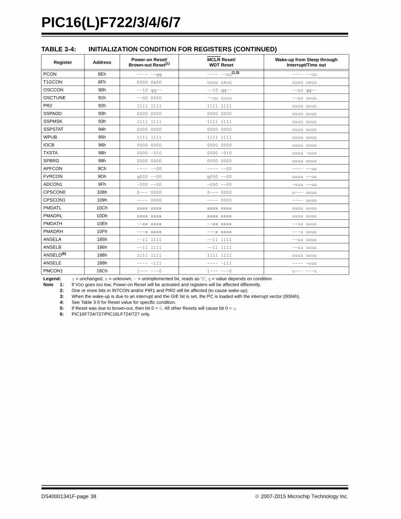
PIC16(L)F722/3/4/6/7
PCON 8Eh ---- --qq ---- --uu(1,5) ---- --uu
T1GCON 8Fh 0000 0x00 uuuu uxuu uuuu uxuu
OSCCON 90h --10 qq-- --10 qq-- --uu qq--
OSCTUNE 91h --00 0000 --uu uuuu --uu uuuu
PR2 92h 1111 1111 1111 1111 uuuu uuuu
SSPADD 93h 0000 0000 0000 0000 uuuu uuuu
SSPMSK 93h 1111 1111 1111 1111 uuuu uuuu
SSPSTAT 94h 0000 0000 0000 0000 uuuu uuuu
WPUB 95h 1111 1111 1111 1111 uuuu uuuu
IOCB 96h 0000 0000 0000 0000 uuuu uuuu
TXSTA 98h 0000 -010 0000 -010 uuuu -uuu
SPBRG 99h 0000 0000 0000 0000 uuuu uuuu
APFCON 9Ch ---- --00 ---- --00 ---- --uu
FVRCON 9Dh q000 --00 q000 --00 uuuu --uu
ADCON1 9Fh -000 --00 -000 --00 -uuu --uu
CPSCON0 108h 0--- 0000 0--- 0000 u--- uuuu
CPSCON1 109h ---- 0000 ---- 0000 ---- uuuu
PMDATL 10Ch xxxx xxxx xxxx xxxx uuuu uuuu
PMADRL 10Dh xxxx xxxx xxxx xxxx uuuu uuuu
PMDATH 10Eh --xx xxxx --xx xxxx --uu uuuu
PMADRH 10Fh ---x xxxx ---x xxxx ---u uuuu
ANSELA 185h --11 1111 --11 1111 --uu uuuu
ANSELB 186h --11 1111 --11 1111 --uu uuuu
ANSELD(6) 188h 1111 1111 1111 1111 uuuu uuuu
ANSELE 189h ---- -111 ---- -111 ---- -uuu
PMCON1 18Ch 1--- ---0 1--- ---0 u--- ---u
TABLE 3-4: INITIALIZATION CONDITION FOR REGISTERS (CONTINUED)
Register AddressPower-on Reset/
Brown-out Reset(1)MCLR Reset/WDT Reset
Wake-up from Sleep through Interrupt/Time out
Legend: u = unchanged, x = unknown, - = unimplemented bit, reads as ‘0’, q = value depends on condition.Note 1: If VDD goes too low, Power-on Reset will be activated and registers will be affected differently.
2: One or more bits in INTCON and/or PIR1 and PIR2 will be affected (to cause wake-up).3: When the wake-up is due to an interrupt and the GIE bit is set, the PC is loaded with the interrupt vector (0004h).4: See Table 3-5 for Reset value for specific condition.5: If Reset was due to brown-out, then bit 0 = 0. All other Resets will cause bit 0 = u.6: PIC16F724/727/PIC16LF724/727 only.
DS40001341F-page 38 2007-2015 Microchip Technology Inc.

PIC16(L)F722/3/4/6/7
TABLE 3-5: INITIALIZATION CONDITION FOR SPECIAL REGISTERS
TABLE 3-6: SUMMARY OF REGISTERS ASSOCIATED WITH RESETS
ConditionProgramCounter
STATUSRegister
PCONRegister
Power-on Reset 0000h 0001 1xxx ---- --0x
MCLR Reset during normal operation 0000h 000u uuuu ---- --uu
MCLR Reset during Sleep 0000h 0001 0uuu ---- --uu
WDT Reset 0000h 0000 uuuu ---- --uu
WDT Wake-up PC + 1 uuu0 0uuu ---- --uu
Brown-out Reset 0000h 0001 1xxx ---- --10
Interrupt Wake-up from Sleep PC + 1(1) uuu1 0uuu ---- --uu
Legend: u = unchanged, x = unknown, - = unimplemented bit, reads as ‘0’.Note 1: When the wake-up is due to an interrupt and Global Interrupt Enable bit, GIE, is set, the PC is loaded with the interrupt
vector (0004h) after execution of PC + 1.
Name Bit 7 Bit 6 Bit 5 Bit 4 Bit 3 Bit 2 Bit 1 Bit 0Value on POR,
BOR
Value on all other Resets(1)
STATUS IRP RP1 RP0 TO PD Z DC C 0001 1xxx 000q quuu
PCON — — — — — — POR BOR ---- --qq ---- --uu
Legend: u = unchanged, x = unknown, - = unimplemented bit, reads as ‘0’, q = value depends on condition. Shaded cells are not used by Resets.
Note 1: Other (non Power-up) Resets include MCLR Reset and Watchdog Timer Reset during normal operation.
2007-2015 Microchip Technology Inc. DS40001341F-page 39
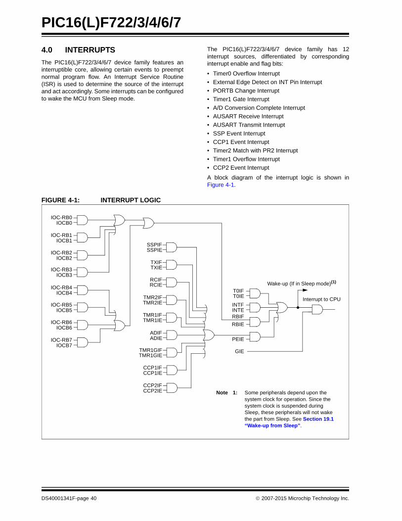
PIC16(L)F722/3/4/6/7
4.0 INTERRUPTS
The PIC16(L)F722/3/4/6/7 device family features aninterruptible core, allowing certain events to preemptnormal program flow. An Interrupt Service Routine(ISR) is used to determine the source of the interruptand act accordingly. Some interrupts can be configuredto wake the MCU from Sleep mode.
The PIC16(L)F722/3/4/6/7 device family has 12interrupt sources, differentiated by correspondinginterrupt enable and flag bits:
• Timer0 Overflow Interrupt
• External Edge Detect on INT Pin Interrupt
• PORTB Change Interrupt
• Timer1 Gate Interrupt
• A/D Conversion Complete Interrupt
• AUSART Receive Interrupt
• AUSART Transmit Interrupt
• SSP Event Interrupt
• CCP1 Event Interrupt
• Timer2 Match with PR2 Interrupt
• Timer1 Overflow Interrupt
• CCP2 Event Interrupt
A block diagram of the interrupt logic is shown inFigure 4-1.
FIGURE 4-1: INTERRUPT LOGIC
T0IFT0IE
INTFINTERBIF
RBIE
GIE
PEIE
Wake-up (If in Sleep mode)(1)
Interrupt to CPU
TMR1GIETMR1GIF
ADIFADIE
IOC-RB0IOCB0
IOC-RB1IOCB1
IOC-RB2IOCB2
IOC-RB3IOCB3
CCP1IFCCP1IE
IOC-RB4IOCB4
IOC-RB5IOCB5
IOC-RB6IOCB6
IOC-RB7IOCB7
RCIFRCIE
TMR2IETMR2IF
SSPIESSPIF
TXIETXIF
TMR1IETMR1IF
Note 1: Some peripherals depend upon the system clock for operation. Since the system clock is suspended during Sleep, these peripherals will not wake the part from Sleep. See Section 19.1 “Wake-up from Sleep”.
CCP2IFCCP2IE
DS40001341F-page 40 2007-2015 Microchip Technology Inc.

PIC16(L)F722/3/4/6/7
4.1 Operation
Interrupts are disabled upon any device Reset. Theyare enabled by setting the following bits:
• GIE bit of the INTCON register
• Interrupt Enable bit(s) for the specific interrupt event(s)
• PEIE bit of the INTCON register (if the Interrupt Enable bit of the interrupt event is contained in the PIE1 and PIE2 registers)
The INTCON, PIR1 and PIR2 registers recordindividual interrupts via Interrupt Flag bits. InterruptFlag bits will be set, regardless of the status of the GIE,PEIE and individual Interrupt Enable bits.
The following events happen when an interrupt eventoccurs while the GIE bit is set:
• Current prefetched instruction is flushed
• GIE bit is cleared
• Current Program Counter (PC) is pushed onto the stack
• PC is loaded with the interrupt vector 0004h
The ISR determines the source of the interrupt bypolling the Interrupt Flag bits. The Interrupt Flag bitsmust be cleared before exiting the ISR to avoidrepeated interrupts. Because the GIE bit is cleared, any
interrupt that occurs while executing the ISR will berecorded through its Interrupt Flag, but will not causethe processor to redirect to the interrupt vector.
The RETFIE instruction exits the ISR by popping theprevious address from the stack and setting the GIE bit.
For additional information on a specific interrupt’soperation, refer to its peripheral chapter.
4.2 Interrupt Latency
Interrupt latency is defined as the time from when theinterrupt event occurs to the time code execution at theinterrupt vector begins. The latency for synchronousinterrupts is three instruction cycles. For asynchronousinterrupts, the latency is three to four instruction cycles,depending on when the interrupt occurs. See Figure 4-2for timing details.
FIGURE 4-2: INT PIN INTERRUPT TIMING
Note 1: Individual Interrupt Flag bits are set,regardless of the state of any otherenable bits.
2: All interrupts will be ignored while the GIEbit is cleared. Any interrupt occurringwhile the GIE bit is clear will be servicedwhen the GIE bit is set again.
Q2Q1 Q3 Q4 Q2Q1 Q3 Q4 Q2Q1 Q3 Q4 Q2Q1 Q3 Q4 Q2Q1 Q3 Q4
OSC1
CLKOUT
INT pin
INTF flag(INTCON<1>)
GIE bit(INTCON<7>)
INSTRUCTION FLOW
PC
InstructionFetched
InstructionExecuted
Interrupt Latency
PC PC + 1 PC + 1 0004h 0005h
Inst (0004h) Inst (0005h)
Dummy Cycle
Inst (PC) Inst (PC + 1)
Inst (PC – 1) Inst (0004h)Dummy CycleInst (PC)
—
Note 1: INTF flag is sampled here (every Q1).
2: Asynchronous interrupt latency = 3-4 TCY. Synchronous latency = 3 TCY, where TCY = instruction cycle time. Latencyis the same whether Inst (PC) is a single cycle or a 2-cycle instruction.
3: CLKOUT is available only in INTOSC and RC Oscillator modes.
4: For minimum width of INT pulse, refer to AC specifications in Section 23.0 “Electrical Specifications”.
5: INTF is enabled to be set any time during the Q4-Q1 cycles.
(1)
(2)
(3)
(4)
(5)(1)
2007-2015 Microchip Technology Inc. DS40001341F-page 41

PIC16(L)F722/3/4/6/7
4.3 Interrupts During Sleep
Some interrupts can be used to wake from Sleep. Towake from Sleep, the peripheral must be able tooperate without the system clock. The interrupt sourcemust have the appropriate Interrupt Enable bit(s) setprior to entering Sleep.
On waking from Sleep, if the GIE bit is also set, theprocessor will branch to the interrupt vector. Otherwise,the processor will continue executing instructions afterthe SLEEP instruction. The instruction directly after theSLEEP instruction will always be executed beforebranching to the ISR. Refer to the Section 19.0“Power-Down Mode (Sleep)” for more details.
4.4 INT Pin
The external interrupt, INT pin, causes anasynchronous, edge-triggered interrupt. The INTEDG bitof the OPTION register determines on which edge theinterrupt will occur. When the INTEDG bit is set, therising edge will cause the interrupt. When the INTEDGbit is clear, the falling edge will cause the interrupt. TheINTF bit of the INTCON register will be set when a validedge appears on the INT pin. If the GIE and INTE bitsare also set, the processor will redirect programexecution to the interrupt vector. This interrupt isdisabled by clearing the INTE bit of the INTCON register.
4.5 Context Saving
When an interrupt occurs, only the return PC value issaved to the stack. If the ISR modifies or uses aninstruction that modifies key registers, their valuesmust be saved at the beginning of the ISR and restoredwhen the ISR completes. This prevents instructionsfollowing the ISR from using invalid data. Examples ofkey registers include the W, STATUS, FSR andPCLATH registers.
The code shown in Example 4-1 can be used to do thefollowing.
• Save the W register
• Save the STATUS register
• Save the PCLATH register
• Execute the ISR program
• Restore the PCLATH register
• Restore the STATUS register
• Restore the W register
Since most instructions modify the W register, it mustbe saved immediately upon entering the ISR. TheSWAPF instruction is used when saving and restoringthe W and STATUS registers because it will not affectany bits in the STATUS register. It is useful to placeW_TEMP in shared memory because the ISR cannotpredict which bank will be selected when the interruptoccurs.
The processor will branch to the interrupt vector byloading the PC with 0004h. The PCLATH register willremain unchanged. This requires the ISR to ensurethat the PCLATH register is set properly before usingan instruction that causes PCLATH to be loaded intothe PC. See Section 2.3 “PCL and PCLATH” fordetails on PC operation.
Note: The microcontroller does not normallyrequire saving the PCLATH register.However, if computed GOTO’s are used,the PCLATH register must be saved at thebeginning of the ISR and restored whenthe ISR is complete to ensure correctprogram flow.
DS40001341F-page 42 2007-2015 Microchip Technology Inc.

PIC16(L)F722/3/4/6/7
EXAMPLE 4-1: SAVING W, STATUS AND PCLATH REGISTERS IN RAM
4.5.1 INTCON REGISTER
The INTCON register is a readable and writableregister, which contains the various enable and flag bitsfor TMR0 register overflow, PORTB change andexternal RB0/INT/SEG0 pin interrupts.
MOVWF W_TEMP ;Copy W to W_TEMP registerSWAPF STATUS,W ;Swap status to be saved into W
;Swaps are used because they do not affect the status bitsBANKSEL STATUS_TEMP ;Select regardless of current bankMOVWF STATUS_TEMP ;Copy status to bank zero STATUS_TEMP registerMOVF PCLATH,W ;Copy PCLATH to W registerMOVWF PCLATH_TEMP ;Copy W register to PCLATH_TEMP::(ISR) ;Insert user code here:BANKSEL STATUS_TEMP ;Select regardless of current bankMOVF PCLATH_TEMP,W ;MOVWF PCLATH ;Restore PCLATHSWAPF STATUS_TEMP,W ;Swap STATUS_TEMP register into W
;(sets bank to original state)MOVWF STATUS ;Move W into STATUS registerSWAPF W_TEMP,F ;Swap W_TEMPSWAPF W_TEMP,W ;Swap W_TEMP into W
Note: Interrupt flag bits are set when an interruptcondition occurs, regardless of the state ofits corresponding enable bit or the globalenable bit, GIE of the INTCON register.User software should ensure theappropriate interrupt flag bits are clearprior to enabling an interrupt.
2007-2015 Microchip Technology Inc. DS40001341F-page 43
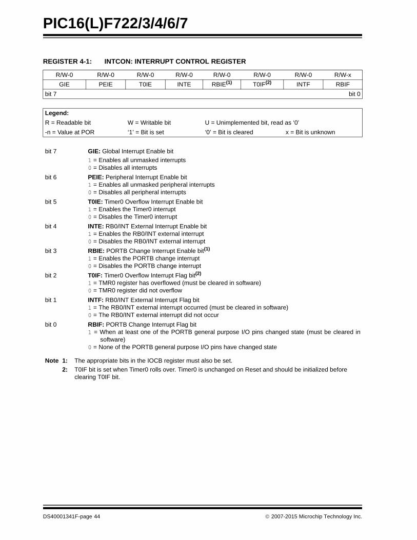
PIC16(L)F722/3/4/6/7
REGISTER 4-1: INTCON: INTERRUPT CONTROL REGISTER
R/W-0 R/W-0 R/W-0 R/W-0 R/W-0 R/W-0 R/W-0 R/W-x
GIE PEIE T0IE INTE RBIE(1) T0IF(2) INTF RBIF
bit 7 bit 0
Legend:
R = Readable bit W = Writable bit U = Unimplemented bit, read as ‘0’
-n = Value at POR ‘1’ = Bit is set ‘0’ = Bit is cleared x = Bit is unknown
bit 7 GIE: Global Interrupt Enable bit
1 = Enables all unmasked interrupts0 = Disables all interrupts
bit 6 PEIE: Peripheral Interrupt Enable bit1 = Enables all unmasked peripheral interrupts0 = Disables all peripheral interrupts
bit 5 T0IE: Timer0 Overflow Interrupt Enable bit1 = Enables the Timer0 interrupt0 = Disables the Timer0 interrupt
bit 4 INTE: RB0/INT External Interrupt Enable bit1 = Enables the RB0/INT external interrupt0 = Disables the RB0/INT external interrupt
bit 3 RBIE: PORTB Change Interrupt Enable bit(1)
1 = Enables the PORTB change interrupt0 = Disables the PORTB change interrupt
bit 2 T0IF: Timer0 Overflow Interrupt Flag bit(2)
1 = TMR0 register has overflowed (must be cleared in software)0 = TMR0 register did not overflow
bit 1 INTF: RB0/INT External Interrupt Flag bit1 = The RB0/INT external interrupt occurred (must be cleared in software)0 = The RB0/INT external interrupt did not occur
bit 0 RBIF: PORTB Change Interrupt Flag bit1 = When at least one of the PORTB general purpose I/O pins changed state (must be cleared in
software)0 = None of the PORTB general purpose I/O pins have changed state
Note 1: The appropriate bits in the IOCB register must also be set.
2: T0IF bit is set when Timer0 rolls over. Timer0 is unchanged on Reset and should be initialized before clearing T0IF bit.
DS40001341F-page 44 2007-2015 Microchip Technology Inc.

PIC16(L)F722/3/4/6/7
4.5.2 PIE1 REGISTER
The PIE1 register contains the interrupt enable bits, asshown in Register 4-2.
Note: Bit PEIE of the INTCON register must beset to enable any peripheral interrupt.
REGISTER 4-2: PIE1: PERIPHERAL INTERRUPT ENABLE REGISTER 1
R/W-0 R/W-0 R/W-0 R/W-0 R/W-0 R/W-0 R/W-0 R/W-0
TMR1GIE ADIE RCIE TXIE SSPIE CCP1IE TMR2IE TMR1IE
bit 7 bit 0
Legend:
R = Readable bit W = Writable bit U = Unimplemented bit, read as ‘0’
-n = Value at POR ‘1’ = Bit is set ‘0’ = Bit is cleared x = Bit is unknown
bit 7 TMR1GIE: Timer1 Gate Interrupt Enable bit
1 = Enable the Timer1 Gate Acquisition complete interrupt0 = Disable the Timer1 Gate Acquisition complete interrupt
bit 6 ADIE: A/D Converter (ADC) Interrupt Enable bit
1 = Enables the ADC interrupt0 = Disables the ADC interrupt
bit 5 RCIE: USART Receive Interrupt Enable bit
1 = Enables the USART receive interrupt0 = Disables the USART receive interrupt
bit 4 TXIE: USART Transmit Interrupt Enable bit
1 = Enables the USART transmit interrupt0 = Disables the USART transmit interrupt
bit 3 SSPIE: Synchronous Serial Port (SSP) Interrupt Enable bit
1 = Enables the SSP interrupt0 = Disables the SSP interrupt
bit 2 CCP1IE: CCP1 Interrupt Enable bit
1 = Enables the CCP1 interrupt0 = Disables the CCP1 interrupt
bit 1 TMR2IE: TMR2 to PR2 Match Interrupt Enable bit
1 = Enables the Timer2 to PR2 match interrupt0 = Disables the Timer2 to PR2 match interrupt
bit 0 TMR1IE: Timer1 Overflow Interrupt Enable bit
1 = Enables the Timer1 overflow interrupt0 = Disables the Timer1 overflow interrupt
2007-2015 Microchip Technology Inc. DS40001341F-page 45

PIC16(L)F722/3/4/6/7
4.5.3 PIE2 REGISTER
The PIE2 register contains the interrupt enable bits, asshown in Register 4-3.
Note: Bit PEIE of the INTCON register must beset to enable any peripheral interrupt.
REGISTER 4-3: PIE2: PERIPHERAL INTERRUPT ENABLE REGISTER 2
U-0 U-0 U-0 U-0 U-0 U-0 U-0 R/W-0
— — — — — — — CCP2IE
bit 7 bit 0
Legend:
R = Readable bit W = Writable bit U = Unimplemented bit, read as ‘0’
-n = Value at POR ‘1’ = Bit is set ‘0’ = Bit is cleared x = Bit is unknown
bit 7-1 Unimplemented: Read as ‘0’
bit 0 CCP2IE: CCP2 Interrupt Enable bit
1 = Enables the CCP2 interrupt0 = Disables the CCP2 interrupt
DS40001341F-page 46 2007-2015 Microchip Technology Inc.

PIC16(L)F722/3/4/6/7
4.5.4 PIR1 REGISTER
The PIR1 register contains the interrupt flag bits, asshown in Register 4-4.
Note: Interrupt flag bits are set when an interruptcondition occurs, regardless of the state ofits corresponding enable bit or the GlobalEnable bit, GIE of the INTCON register.User software should ensure theappropriate interrupt flag bits are clear priorto enabling an interrupt.
REGISTER 4-4: PIR1: PERIPHERAL INTERRUPT REQUEST REGISTER 1
R/W-0 R/W-0 R-0 R-0 R/W-0 R/W-0 R/W-0 R/W-0
TMR1GIF ADIF RCIF TXIF SSPIF CCP1IF TMR2IF TMR1IF
bit 7 bit 0
Legend:
R = Readable bit W = Writable bit U = Unimplemented bit, read as ‘0’
-n = Value at POR ‘1’ = Bit is set ‘0’ = Bit is cleared x = Bit is unknown
bit 7 TMR1GIF: Timer1 Gate Interrupt Flag bit
1 = Timer1 Gate is inactive0 = Timer1 Gate is active
bit 6 ADIF: A/D Converter Interrupt Flag bit
1 = A/D conversion complete (must be cleared in software)0 = A/D conversion has not completed or has not been started
bit 5 RCIF: USART Receive Interrupt Flag bit
1 = The USART receive buffer is full (cleared by reading RCREG)0 = The USART receive buffer is not full
bit 4 TXIF: USART Transmit Interrupt Flag bit
1 = The USART transmit buffer is empty (cleared by writing to TXREG)0 = The USART transmit buffer is full
bit 3 SSPIF: Synchronous Serial Port (SSP) Interrupt Flag bit
1 = The Transmission/Reception is complete (must be cleared in software)0 = Waiting to Transmit/Receive
bit 2 CCP1IF: CCP1 Interrupt Flag bit
Capture mode:
1 = A TMR1 register capture occurred (must be cleared in software)0 = No TMR1 register capture occurred
Compare mode:
1 = A TMR1 register compare match occurred (must be cleared in software)0 = No TMR1 register compare match occurred
PWM mode:Unused in this mode
bit 1 TMR2IF: Timer2 to PR2 Interrupt Flag bit
1 = A Timer2 to PR2 match occurred (must be cleared in software)0 = No Timer2 to PR2 match occurred
bit 0 TMR1IF: Timer1 Overflow Interrupt Flag bit
1 = The TMR1 register overflowed (must be cleared in software)0 = The TMR1 register did not overflow
2007-2015 Microchip Technology Inc. DS40001341F-page 47

PIC16(L)F722/3/4/6/7
4.5.5 PIR2 REGISTER
The PIR2 register contains the interrupt flag bits, asshown in Register 4-5.
TABLE 4-1: SUMMARY OF REGISTERS ASSOCIATED WITH INTERRUPTS
Note: Interrupt flag bits are set when an interruptcondition occurs, regardless of the state ofits corresponding enable bit or the GlobalEnable bit, GIE of the INTCON register.User software should ensure theappropriate interrupt flag bits are clear priorto enabling an interrupt.
REGISTER 4-5: PIR2: PERIPHERAL INTERRUPT REQUEST REGISTER 2
U-0 U-0 U-0 U-0 U-0 U-0 U-0 R/W-0
— — — — — — — CCP2IF
bit 7 bit 0
Legend:
R = Readable bit W = Writable bit U = Unimplemented bit, read as ‘0’
-n = Value at POR ‘1’ = Bit is set ‘0’ = Bit is cleared x = Bit is unknown
bit 7-1 Unimplemented: Read as ‘0’
bit 0 CCP2IF: CCP2 Interrupt Flag bit
Capture Mode:
1 = A TMR1 register capture occurred (must be cleared in software)0 = No TMR1 register capture occurred
Compare Mode:
1 = A TMR1 register compare match occurred (must be cleared in software)0 = No TMR1 register compare match occurred
PWM mode:
Unused in this mode
Name Bit 7 Bit 6 Bit 5 Bit 4 Bit 3 Bit 2 Bit 1 Bit 0Value on
POR, BOR
Value onall otherResets
INTCON GIE PEIE T0IE INTE RBIE T0IF INTF RBIF 0000 000x 0000 000x
OPTION_REG RBPU INTEDG T0CS T0SE PSA PS2 PS1 PS0 1111 1111 1111 1111
PIE1 TMR1GIE ADIE RCIE TXIE SSPIE CCP1IE TMR2IE TMR1IE 0000 0000 0000 0000
PIE2 — — — — — — — CCP2IE ---- ---0 ---- ---0
PIR1 TMR1GIF ADIF RCIF TXIF SSPIF CCP1IF TMR2IF TMR1IF 0000 0000 0000 0000
PIR2 — — — — — — — CCP2IF ---- ---0 ---- ---0
Legend: - = Unimplemented locations, read as ‘0’, u = unchanged, x = unknown. Shaded cells are not used by the Capture, Compare and PWM.
DS40001341F-page 48 2007-2015 Microchip Technology Inc.

2007-2015 Microchip Technology Inc. DS40001341F-page 49
PIC16(L)F722/3/4/6/7
5.0 LOW DROPOUT (LDO) VOLTAGE REGULATOR
The PIC16F722/3/4/6/7 devices differ from thePIC16LF722/3/4/6/7 devices due to an internal LowDropout (LDO) voltage regulator. The PIC16F722/3/4/6/7 devices contain an internal LDO, while thePIC16LF722/3/4/6/7 ones do not.
The lithography of the die allows a maximum operatingvoltage of 3.6V on the internal digital logic. In order tocontinue to support 5.0V designs, a LDO voltageregulator is integrated on the die. The LDO voltageregulator allows for the internal digital logic to operateat 3.2V, while I/O’s operate at 5.0V (VDD).
The LDO voltage regulator requires an external bypasscapacitor for stability. One of three pins, denoted asVCAP, can be configured for the external bypasscapacitor. It is recommended that the capacitor be aceramic cap between 0.1 to 1.0 µF. The VCAP pin is notintended to supply power to external loads. An externalvoltage regulator should be used if this functionality isrequired. In addition, external devices should notsupply power to the VCAP pin.
On power-up, the external capacitor will look like alarge load on the LDO voltage regulator. To preventerroneous operation, the device is held in Reset whilea constant current source charges the externalcapacitor. After the cap is fully charged, the device isreleased from Reset. For more information, refer toSection 23.0 “Electrical Specifications”.
See Configuration Word 2 register (Register 8-2) forVCAP enable bits.

PIC16(L)F722/3/4/6/7
6.0 I/O PORTS
There are as many as 35 general purpose I/O pinsavailable. Depending on which peripherals areenabled, some or all of the pins may not be available asgeneral purpose I/O. In general, when a peripheral isenabled, the associated pin may not be used as ageneral purpose I/O pin.
6.1 Alternate Pin Function
The Alternate Pin Function Control (APFCON) registeris used to steer specific peripheral input and outputfunctions between different pins. The APFCON registeris shown in Register 6-1. For this device family, thefollowing functions can be moved between differentpins.
• SS (Slave Select)
• CCP2
REGISTER 6-1: APFCON: ALTERNATE PIN FUNCTION CONTROL REGISTER
U-0 U-0 U-0 U-0 U-0 U-0 R/W-0 R/W-0
— — — — — — SSSEL CCP2SEL
bit 7 bit 0
Legend:
R = Readable bit W = Writable bit U = Unimplemented bit, read as ‘0’
-n = Value at POR ‘1’ = Bit is set ‘0’ = Bit is cleared x = Bit is unknown
bit 7-2 Unimplemented: Read as ‘0’.
bit 1 SSSEL: SS Input Pin Selection bit
0 = SS function is on RA5/AN4/CPS7/SS/VCAP
1 = SS function is on RA0/AN0/SS/VCAP
bit 0 CCP2SEL: CCP2 Input/Output Pin Selection bit
0 = CCP2 function is on RC1/T1OSI/CCP21 = CCP2 function is on RB3/CCP2
DS40001341F-page 50 2007-2015 Microchip Technology Inc.

PIC16(L)F722/3/4/6/7
6.2 PORTA and the TRISA Registers
PORTA is a 8-bit wide, bidirectional port. Thecorresponding data direction register is TRISA(Register 6-3). Setting a TRISA bit (= 1) will make thecorresponding PORTA pin an input (i.e., disable theoutput driver). Clearing a TRISA bit (= 0) will make thecorresponding PORTA pin an output (i.e., enablesoutput driver and puts the contents of the output latchon the selected pin). Example 6-1 shows how toinitialize PORTA.
Reading the PORTA register (Register 6-2) reads thestatus of the pins, whereas writing to it will write to thePORT latch. All write operations are read-modify-writeoperations. Therefore, a write to a port implies that theport pins are read, this value is modified and thenwritten to the PORT data latch.
The TRISA register (Register 6-3) controls the PORTApin output drivers, even when they are being used asanalog inputs. The user should ensure the bits in the
TRISA register are maintained set when using them asanalog inputs. I/O pins configured as analog input alwaysread ‘0’.
EXAMPLE 6-1: INITIALIZING PORTA
Note: The ANSELA register must be initializedto configure an analog channel as a digitalinput. Pins configured as analog inputswill read ‘0’.
BANKSEL PORTA ;CLRF PORTA ;Init PORTABANKSEL ANSELA ;CLRF ANSELA ;digital I/OBANKSEL TRISA ;MOVLW 0Ch ;Set RA<3:2> as inputsMOVWF TRISA ;and set RA<7:4,1:0>
;as outputs
REGISTER 6-2: PORTA: PORTA REGISTER
R/W-x R/W-x R/W-x R/W-x R/W-x R/W-x R/W-x R/W-x
RA7 RA6 RA5 RA4 RA3 RA2 RA1 RA0
bit 7 bit 0
Legend:
R = Readable bit W = Writable bit U = Unimplemented bit, read as ‘0’
-n = Value at POR ‘1’ = Bit is set ‘0’ = Bit is cleared x = Bit is unknown
bit 7-0 RA<7:0>: PORTA I/O Pin bit1 = Port pin is > VIH
0 = Port pin is < VIL
REGISTER 6-3: TRISA: PORTA TRI-STATE REGISTER
R/W-1 R/W-1 R/W-1 R/W-1 R/W-1 R/W-1 R/W-1 R/W-1
TRISA7 TRISA6 TRISA5 TRISA4 TRISA3 TRISA2 TRISA1 TRISA0
bit 7 bit 0
Legend:
R = Readable bit W = Writable bit U = Unimplemented bit, read as ‘0’
-n = Value at POR ‘1’ = Bit is set ‘0’ = Bit is cleared x = Bit is unknown
bit 7-0 TRISA<7:0>: PORTA Tri-State Control bit1 = PORTA pin configured as an input (tri-stated)0 = PORTA pin configured as an output
2007-2015 Microchip Technology Inc. DS40001341F-page 51

PIC16(L)F722/3/4/6/7
6.2.1 ANSELA REGISTER
The ANSELA register (Register 6-4) is used toconfigure the Input mode of an I/O pin to analog.Setting the appropriate ANSELA bit high will cause alldigital reads on the pin to be read as ‘0’ and allowanalog functions on the pin to operate correctly.
The state of the ANSELA bits has no affect on digitaloutput functions. A pin with TRIS clear and ANSEL setwill still operate as a digital output, but the Input modewill be analog. This can cause unexpected behaviorwhen executing read-modify-write instructions on theaffected port.
REGISTER 6-4: ANSELA: PORTA ANALOG SELECT REGISTER
U-0 U-0 R/W-1 R/W-1 R/W-1 R/W-1 R/W-1 R/W-1
— — ANSA5 ANSA4 ANSA3 ANSA2 ANSA1 ANSA0
bit 7 bit 0
Legend:
R = Readable bit W = Writable bit U = Unimplemented bit, read as ‘0’
-n = Value at POR ‘1’ = Bit is set ‘0’ = Bit is cleared x = Bit is unknown
bit 7-6 Unimplemented: Read as ‘0’
bit 5-0 ANSA<5:0>: Analog Select between Analog or Digital Function on pins RA<5:0>, respectively
0 = Digital I/O. Pin is assigned to port or Digital special function.1 = Analog input. Pin is assigned as analog input(1). Digital Input buffer disabled.
Note 1: When setting a pin to an analog input, the corresponding TRIS bit must be set to Input mode in order to allow external control of the voltage on the pin.
DS40001341F-page 52 2007-2015 Microchip Technology Inc.

PIC16(L)F722/3/4/6/7
6.2.2 PIN DESCRIPTIONS AND DIAGRAMS
Each PORTA pin is multiplexed with other functions. Thepins and their combined functions are briefly describedhere. For specific information about individual functionssuch as the A/D Converter (ADC), refer to theappropriate section in this data sheet.
6.2.2.1 RA0/AN0/SS/VCAP
Figure 6-1 shows the diagram for this pin. This pin isconfigurable to function as one of the following:
• a general purpose I/O
• an analog input for the ADC
• a slave select input for the SSP(1)
• a Voltage Regulator Capacitor pin (PIC16F72X only)
6.2.2.2 RA1/AN1
Figure 6-2 shows the diagram for this pin. This pin isconfigurable to function as one of the following:
• a general purpose I/O
• an analog input for the ADC
6.2.2.3 RA2/AN2
Figure 6-2 shows the diagram for this pin. This pin isconfigurable to function as one of the following:
• a general purpose I/O
• an analog input for the ADC
6.2.2.4 RA3/AN3/VREF
Figure 6-2 shows the diagram for this pin. This pin isconfigurable to function as one of the following:
• a general purpose I/O
• an analog input for the ADC
• a voltage reference input for the ADC
6.2.2.5 RA4/CPS6/T0CKI
Figure 6-3 shows the diagram for this pin. This pin isconfigurable to function as one of the following:
• a general purpose I/O
• a capacitive sensing input
• a clock input for Timer0
The Timer0 clock input function works independentlyof any TRIS register setting. Effectively, if TRISA4 = 0,the PORTA4 register bit will output to the pad andClock Timer0 at the same time.
6.2.2.6 RA5/AN4/CPS7/SS/VCAP
Figure 6-4 shows the diagram for this pin. This pin isconfigurable to function as one of the following:
• a general purpose I/O
• an analog input for the ADC
• a capacitive sensing input
• a slave select input for the SSP(1)
• a Voltage Regulator Capacitor pin (PIC16F72X only)
6.2.2.7 RA6/OSC2/CLKOUT/VCAP
Figure 6-5 shows the diagram for this pin. This pin isconfigurable to function as one of the following:
• a general purpose I/O
• a crystal/resonator connection
• a clock output
• a Voltage Regulator Capacitor pin (PIC16F72X only)
6.2.2.8 RA7/OSC1/CLKIN
Figure 6-6 shows the diagram for this pin. This pin isconfigurable to function as one of the following:
• a general purpose I/O
• a crystal/resonator connection
• a clock input
Note: SS pin location may be selected as RA5or RA0.
Note: SS pin location may be selected as RA5or RA0.
2007-2015 Microchip Technology Inc. DS40001341F-page 53

PIC16(L)F722/3/4/6/7
FIGURE 6-1: BLOCK DIAGRAM OF RA0
I/O Pin
VDD
VSS
D
QCK
Q
D
QCK
Q
RD
WR
WR
RD
ANSA0
Data Bus
PORTA
TRISA
TRISA
PORTA
To SSP SS Input
To A/D Converter
VCAPEN = 00
To Voltage RegulatorPIC16F72X only
DS40001341F-page 54 2007-2015 Microchip Technology Inc.

PIC16(L)F722/3/4/6/7
FIGURE 6-2: RA<3:1> BLOCK DIAGRAM
FIGURE 6-3: BLOCK DIAGRAM OF RA4
I/O Pin
VDD
VSS
D
QCK
Q
D
QCK
Q
RD
WR
WR
RD
ANSAx
Data Bus
PORTA
TRISA
TRISA
PORTA
To A/D Converter
I/O Pin
VDD
VSS
D
QCK
Q
D
QCK
Q
RD
WR
WR
RD
ANSA4
Data Bus
PORTA
TRISA
TRISA
PORTA
To Timer0 Clock MUX
To Cap Sensor
2007-2015 Microchip Technology Inc. DS40001341F-page 55

PIC16(L)F722/3/4/6/7
FIGURE 6-4: BLOCK DIAGRAM OF RA5
I/O Pin
VDD
VSS
D
QCK
Q
D
QCK
Q
RD
WR
WR
RD
ANSA5
Data Bus
PORTA
TRISA
TRISA
PORTA
To SSP SS Input
To A/D Converter
VCAPEN = 01
To Voltage RegulatorPIC16F72X only
To Cap Sensor
DS40001341F-page 56 2007-2015 Microchip Technology Inc.
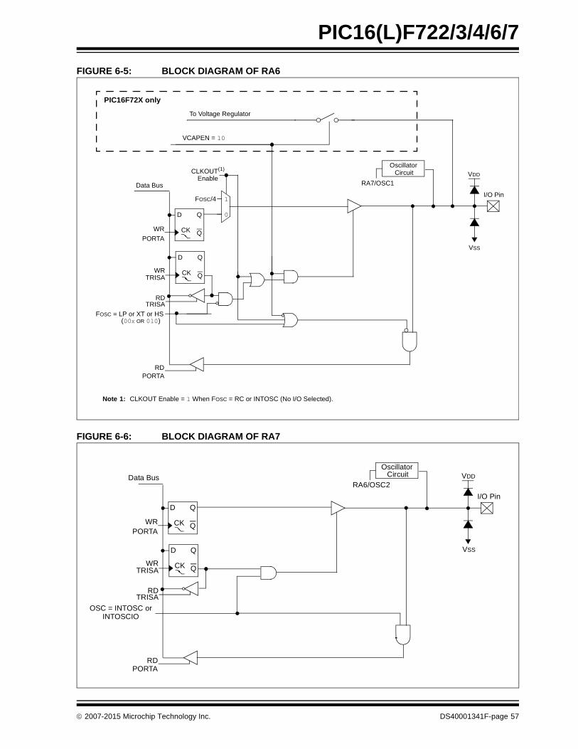
PIC16(L)F722/3/4/6/7
FIGURE 6-5: BLOCK DIAGRAM OF RA6
FIGURE 6-6: BLOCK DIAGRAM OF RA7
0
1I/O Pin
VDD
VSS
D
QCK
Q
D
QCK
Q
RD
WR
WR
RD
FOSC = LP or XT or HS
Data Bus
PORTA
TRISA
TRISA
PORTA
FOSC/4
CLKOUT(1)
Enable
Note 1: CLKOUT Enable = 1 When FOSC = RC or INTOSC (No I/O Selected).
OscillatorCircuit
RA7/OSC1
VCAPEN = 10
To Voltage Regulator
(00X OR 010)
PIC16F72X only
I/O Pin
VDD
VSS
D
QCK
Q
D
QCK
Q
RD
WR
WR
RD
OSC = INTOSC or
Data Bus
PORTA
TRISA
TRISA
PORTA
OscillatorCircuit
RA6/OSC2
INTOSCIO
2007-2015 Microchip Technology Inc. DS40001341F-page 57

PIC16(L)F722/3/4/6/7
TABLE 6-1: SUMMARY OF REGISTERS ASSOCIATED WITH PORTA
Name Bit 7 Bit 6 Bit 5 Bit 4 Bit 3 Bit 2 Bit 1 Bit 0Value on
POR, BOR
Value on all other Resets
ADCON0 — — CHS3 CHS2 CHS1 CHS0 GO/DONE ADON 0000 0000 0000 0000
ADCON1 — ADCS2 ADCS1 ADCS0 — — ADREF1 ADREF0 -000 --00 -000 --00
ANSELA — — ANSA5 ANSA4 ANSA3 ANSA2 ANSA1 ANSA0 --11 1111 --11 1111
APFCON — — — — — — SSSEL CCP2SEL ---- --00 ---- --00
CPSCON0 CPSON — — — CPSRNG1 CPSRNG0 CPSOUT T0XCS 0--- 0000 0--- 0000
CPSCON1 — — — — CPSCH3 CPSCH2 CPSCH1 CPSCH0 ---- 0000 ---- 0000
CONFIG2(1) — — VCAPEN1 VCAPEN0 — — — — — —
OPTION_REG RBPU INTEDG T0CS T0SE PSA PS2 PS1 PS0 1111 1111 1111 1111
PORTA RA7 RA6 RA5 RA4 RA3 RA2 RA1 RA0 xxxx xxxx xxxx xxxx
SSPCON WCOL SSPOV SSPEN CKP SSPM3 SSPM2 SSPM1 SSPM0 0000 0000 0000 0000
TRISA TRISA7 TRISA6 TRISA5 TRISA4 TRISA3 TRISA2 TRISA1 TRISA0 1111 1111 1111 1111
Legend: x = unknown, u = unchanged, – = unimplemented locations read as ‘0’. Shaded cells are not used by PORTA.Note 1: PIC16F72X only.
DS40001341F-page 58 2007-2015 Microchip Technology Inc.
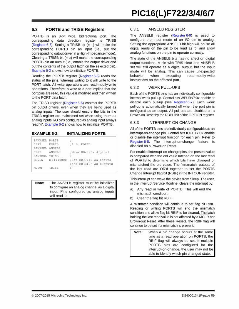
PIC16(L)F722/3/4/6/7
6.3 PORTB and TRISB Registers
PORTB is an 8-bit wide, bidirectional port. Thecorresponding data direction register is TRISB(Register 6-6). Setting a TRISB bit (= 1) will make thecorresponding PORTB pin an input (i.e., put thecorresponding output driver in a High-Impedance mode).Clearing a TRISB bit (= 0) will make the correspondingPORTB pin an output (i.e., enable the output driver andput the contents of the output latch on the selected pin).Example 6-2 shows how to initialize PORTB.
Reading the PORTB register (Register 6-5) reads thestatus of the pins, whereas writing to it will write to thePORT latch. All write operations are read-modify-writeoperations. Therefore, a write to a port implies that theport pins are read, this value is modified and then writtento the PORT data latch.
The TRISB register (Register 6-6) controls the PORTBpin output drivers, even when they are being used asanalog inputs. The user should ensure the bits in theTRISB register are maintained set when using them asanalog inputs. I/O pins configured as analog input alwaysread ‘0’. Example 6-2 shows how to initialize PORTB.
EXAMPLE 6-2: INITIALIZING PORTB
6.3.1 ANSELB REGISTER
The ANSELB register (Register 6-9) is used toconfigure the Input mode of an I/O pin to analog.Setting the appropriate ANSELB bit high will cause alldigital reads on the pin to be read as ‘0’ and allowanalog functions on the pin to operate correctly.
The state of the ANSELB bits has no affect on digitaloutput functions. A pin with TRIS clear and ANSELBset will still operate as a digital output, but the Inputmode will be analog. This can cause unexpectedbehavior when executing read-modify-writeinstructions on the affected port.
6.3.2 WEAK PULL-UPS
Each of the PORTB pins has an individually configurableinternal weak pull-up. Control bits WPUB<7:0> enable ordisable each pull-up (see Register 6-7). Each weakpull-up is automatically turned off when the port pin isconfigured as an output. All pull-ups are disabled on aPower-on Reset by the RBPU bit of the OPTION register.
6.3.3 INTERRUPT-ON-CHANGE
All of the PORTB pins are individually configurable as aninterrupt-on-change pin. Control bits IOCB<7:0> enableor disable the interrupt function for each pin. Refer toRegister 6-8. The interrupt-on-change feature isdisabled on a Power-on Reset.
For enabled interrupt-on-change pins, the present valueis compared with the old value latched on the last readof PORTB to determine which bits have changed ormismatched the old value. The ‘mismatch’ outputs ofthe last read are OR’d together to set the PORTBChange Interrupt flag bit (RBIF) in the INTCON register.
This interrupt can wake the device from Sleep. The user,in the Interrupt Service Routine, clears the interrupt by:
a) Any read or write of PORTB. This will end themismatch condition.
b) Clear the flag bit RBIF.
A mismatch condition will continue to set flag bit RBIF.Reading or writing PORTB will end the mismatchcondition and allow flag bit RBIF to be cleared. The latchholding the last read value is not affected by a MCLR norBrown-out Reset. After these Resets, the RBIF flag willcontinue to be set if a mismatch is present.
Note: The ANSELB register must be initializedto configure an analog channel as a digitalinput. Pins configured as analog inputswill read ‘0’.
BANKSEL PORTB ;CLRF PORTB ;Init PORTBBANKSEL ANSELBCLRF ANSELB ;Make RB<7:0> digitalBANKSEL TRISB ;MOVLW B’11110000’ ;Set RB<7:4> as inputs
;and RB<3:0> as outputsMOVWF TRISB ;
Note: When a pin change occurs at the sametime as a read operation on PORTB, theRBIF flag will always be set. If multiplePORTB pins are configured for theinterrupt-on-change, the user may not beable to identify which pin changed state.
2007-2015 Microchip Technology Inc. DS40001341F-page 59

PIC16(L)F722/3/4/6/7
REGISTER 6-5: PORTB: PORTB REGISTER
R/W-x R/W-x R/W-x R/W-x R/W-x R/W-x R/W-x R/W-x
RB7 RB6 RB5 RB4 RB3 RB2 RB1 RB0
bit 7 bit 0
Legend:
R = Readable bit W = Writable bit U = Unimplemented bit, read as ‘0’
-n = Value at POR ‘1’ = Bit is set ‘0’ = Bit is cleared x = Bit is unknown
bit 7-0 RB<7:0>: PORTB I/O Pin bit1 = Port pin is > VIH
0 = Port pin is < VIL
REGISTER 6-6: TRISB: PORTB TRI-STATE REGISTER
R/W-1 R/W-1 R/W-1 R/W-1 R/W-1 R/W-1 R/W-1 R/W-1
TRISB7 TRISB6 TRISB5 TRISB4 TRISB3 TRISB2 TRISB1 TRISB0
bit 7 bit 0
Legend:
R = Readable bit W = Writable bit U = Unimplemented bit, read as ‘0’
-n = Value at POR ‘1’ = Bit is set ‘0’ = Bit is cleared x = Bit is unknown
bit 7-0 TRISB<7:0>: PORTB Tri-State Control bit1 = PORTB pin configured as an input (tri-stated)0 = PORTB pin configured as an output
DS40001341F-page 60 2007-2015 Microchip Technology Inc.
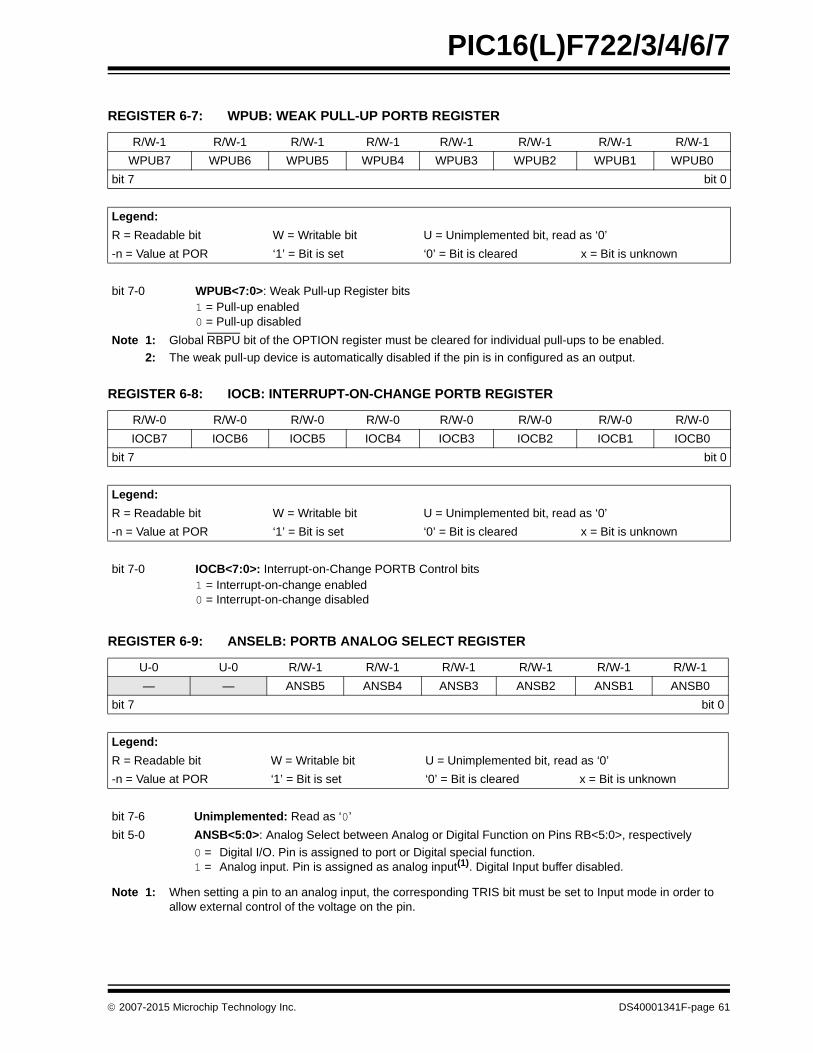
PIC16(L)F722/3/4/6/7
REGISTER 6-7: WPUB: WEAK PULL-UP PORTB REGISTER
R/W-1 R/W-1 R/W-1 R/W-1 R/W-1 R/W-1 R/W-1 R/W-1
WPUB7 WPUB6 WPUB5 WPUB4 WPUB3 WPUB2 WPUB1 WPUB0
bit 7 bit 0
Legend:
R = Readable bit W = Writable bit U = Unimplemented bit, read as ‘0’
-n = Value at POR ‘1’ = Bit is set ‘0’ = Bit is cleared x = Bit is unknown
bit 7-0 WPUB<7:0>: Weak Pull-up Register bits1 = Pull-up enabled0 = Pull-up disabled
Note 1: Global RBPU bit of the OPTION register must be cleared for individual pull-ups to be enabled.
2: The weak pull-up device is automatically disabled if the pin is in configured as an output.
REGISTER 6-8: IOCB: INTERRUPT-ON-CHANGE PORTB REGISTER
R/W-0 R/W-0 R/W-0 R/W-0 R/W-0 R/W-0 R/W-0 R/W-0
IOCB7 IOCB6 IOCB5 IOCB4 IOCB3 IOCB2 IOCB1 IOCB0
bit 7 bit 0
Legend:
R = Readable bit W = Writable bit U = Unimplemented bit, read as ‘0’
-n = Value at POR ‘1’ = Bit is set ‘0’ = Bit is cleared x = Bit is unknown
bit 7-0 IOCB<7:0>: Interrupt-on-Change PORTB Control bits1 = Interrupt-on-change enabled0 = Interrupt-on-change disabled
REGISTER 6-9: ANSELB: PORTB ANALOG SELECT REGISTER
U-0 U-0 R/W-1 R/W-1 R/W-1 R/W-1 R/W-1 R/W-1
— — ANSB5 ANSB4 ANSB3 ANSB2 ANSB1 ANSB0
bit 7 bit 0
Legend:
R = Readable bit W = Writable bit U = Unimplemented bit, read as ‘0’
-n = Value at POR ‘1’ = Bit is set ‘0’ = Bit is cleared x = Bit is unknown
bit 7-6 Unimplemented: Read as ‘0’
bit 5-0 ANSB<5:0>: Analog Select between Analog or Digital Function on Pins RB<5:0>, respectively
0 = Digital I/O. Pin is assigned to port or Digital special function.1 = Analog input. Pin is assigned as analog input(1). Digital Input buffer disabled.
Note 1: When setting a pin to an analog input, the corresponding TRIS bit must be set to Input mode in order to allow external control of the voltage on the pin.
2007-2015 Microchip Technology Inc. DS40001341F-page 61

PIC16(L)F722/3/4/6/7
6.3.4 PIN DESCRIPTIONS AND DIAGRAMS
Each PORTB pin is multiplexed with other functions. Thepins and their combined functions are briefly describedhere. For specific information about individual functionssuch as the SSP, I2C or interrupts, refer to the appropriatesection in this data sheet.
6.3.4.1 RB0/AN12/CPS0/INT
Figure 6-7 shows the diagram for this pin. This pin isconfigurable to function as one of the following:
• a general purpose I/O
• an analog input for the ADC
• a capacitive sensing input
• an external edge triggered interrupt
6.3.4.2 RB1/AN10/CPS1
Figure 6-8 shows the diagram for this pin. This pin isconfigurable to function as one of the following:
• a general purpose I/O
• an analog input for the ADC
• a capacitive sensing input
6.3.4.3 RB2/AN8/CPS2
Figure 6-8 shows the diagram for this pin. This pin isconfigurable to function as one of the following:
• a general purpose I/O
• an analog input for the ADC
• a capacitive sensing input
6.3.4.4 RB3/AN9/CPS3/CCP2
Figure 6-9 shows the diagram for this pin. This pin isconfigurable to function as one of the following:
• a general purpose I/O
• an analog input for the ADC
• a capacitive sensing input
• a Capture 2 input, Compare 2 output, and PWM2 output
6.3.4.5 RB4/AN11/CPS4
Figure 6-8 shows the diagram for this pin. This pin isconfigurable to function as one of the following:
• a general purpose I/O
• an analog input for the ADC
• a capacitive sensing input
6.3.4.6 RB5/AN13/CPS5/T1G
Figure 6-10 shows the diagram for this pin. This pin isconfigurable to function as one of the following:
• a general purpose I/O
• an analog input for the ADC
• a capacitive sensing input
• a Timer1 gate input
6.3.4.7 RB6/ICSPCLK
Figure 6-11 shows the diagram for this pin. This pin isconfigurable to function as one of the following:
• a general purpose I/O
• In-Circuit Serial Programming clock
6.3.4.8 RB7/ICSPDAT
Figure 6-12 shows the diagram for this pin. This pin isconfigurable to function as one of the following:
• a general purpose I/O
• In-Circuit Serial Programming data
Note: CCP2 pin location may be selected asRB3 or RC1.
DS40001341F-page 62 2007-2015 Microchip Technology Inc.
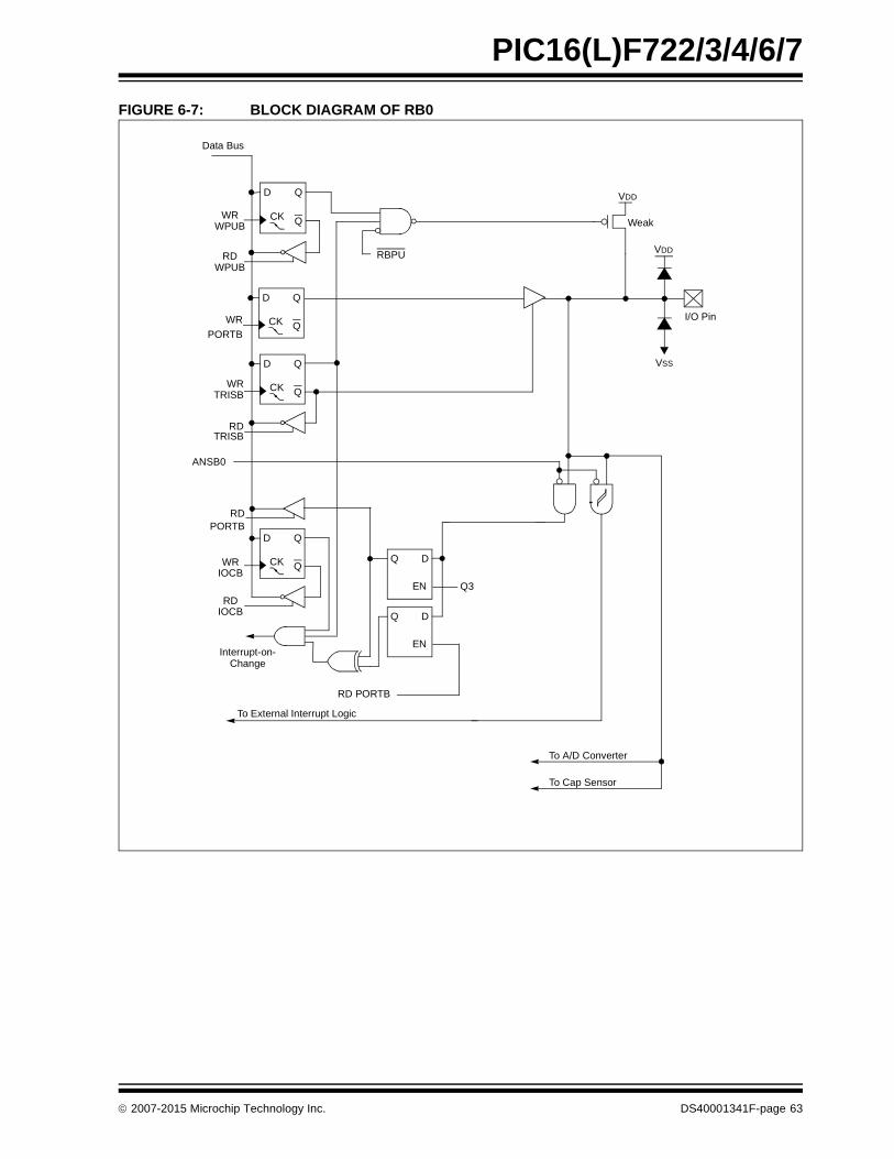
PIC16(L)F722/3/4/6/7
FIGURE 6-7: BLOCK DIAGRAM OF RB0
I/O Pin
VDD
VSS
D
QCK
Q
D
QCK
Q
RD
WR
WR
RD
Data Bus
PORTB
TRISB
TRISB
PORTB
D
QCK
Q VDD
WeakWR
WPUB
RDWPUB
RBPU
D
QCK
Q
D
EN
Q
D
EN
Q
RD PORTB
WRIOCB
RDIOCB
Interrupt-on-Change
Q3
ANSB0
To A/D Converter
To External Interrupt Logic
To Cap Sensor
2007-2015 Microchip Technology Inc. DS40001341F-page 63
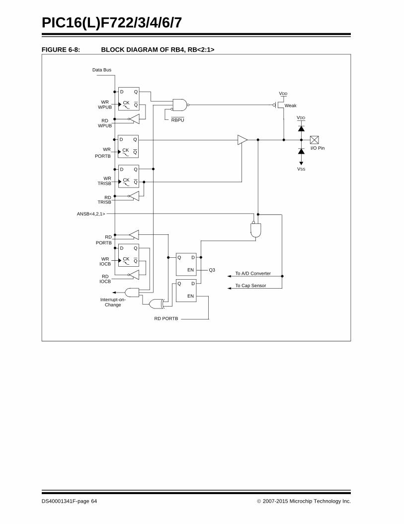
PIC16(L)F722/3/4/6/7
FIGURE 6-8: BLOCK DIAGRAM OF RB4, RB<2:1>
I/O Pin
VDD
VSS
D
QCK
Q
D
QCK
Q
RD
WR
WR
RD
Data Bus
PORTB
TRISB
TRISB
PORTB
D
QCK
Q VDD
WeakWR
WPUB
RDWPUB
RBPU
D
QCK
Q
D
EN
Q
D
EN
Q
RD PORTB
WRIOCB
RDIOCB
Interrupt-on-Change
Q3
ANSB<4,2,1>
To A/D Converter
To Cap Sensor
DS40001341F-page 64 2007-2015 Microchip Technology Inc.

PIC16(L)F722/3/4/6/7
FIGURE 6-9: BLOCK DIAGRAM OF RB3
I/O Pin
VDD
VSS
D
QCK
Q
D
QCK
Q
RD
WR
WR
RD
Data Bus
PORTB
TRISB
TRISB
PORTB
D
QCK
Q VDD
WeakWR
WPUB
RDWPUB
RBPU
D
QCK
Q
D
EN
Q
D
EN
Q
RD PORTB
WRIOCB
RDIOCB
Interrupt-on-Change
Q3
ANSB<5,3>
To CCP2(1)
Note 1: CCP2 input is controlled by CCP2SEL in the APFCON register.
0
1CCP2OUT
CCP2OUTEnable
To A/D Converter
To Cap Sensor
2007-2015 Microchip Technology Inc. DS40001341F-page 65

PIC16(L)F722/3/4/6/7
FIGURE 6-10: BLOCK DIAGRAM OF RB5
I/O Pin
VDD
VSS
D
QCK
Q
D
QCK
Q
RD
WR
WR
RD
Data Bus
PORTB
TRISB
TRISB
PORTB
D
QCK
Q VDD
WeakWR
WPUB
RDWPUB
RBPU
D
QCK
Q
D
EN
Q
D
EN
Q
RD PORTB
WRIOCB
RDIOCB
Interrupt-on-Change
Q3
ANSB<5,3>
To Timer1 Gate
0
1CCP2OUT
CCP2OUTEnable
To A/D Converter
To Cap Sensor
DS40001341F-page 66 2007-2015 Microchip Technology Inc.

PIC16(L)F722/3/4/6/7
FIGURE 6-11: BLOCK DIAGRAM OF RB6
I/O Pin
VDD
VSS
D
QCK
Q
D
QCK
Q
RD
WR
WR
RD
Data Bus
PORTB
TRISB
TRISB
PORTB
D
QCK
Q VDD
WeakWR
WPUB
RDWPUB
RBPU
D
QCK
Q
D
EN
Q
D
EN
Q
RD PORTB
WRIOCB
RDIOCB
Interrupt-on-Change
Q3
ICSP™ MODE
ICSPCLK
0
1
0
1
TRIS_ICDCLK
PORT_ICDCLK
DEBUG
2007-2015 Microchip Technology Inc. DS40001341F-page 67

PIC16(L)F722/3/4/6/7
FIGURE 6-12: BLOCK DIAGRAM OF RB7
I/O Pin
VDD
VSS
D
QCK
Q
D
QCK
Q
RD
WR
WR
RD
Data Bus
PORTB
TRISB
TRISB
PORTB
D
QCK
Q VDD
WeakWR
WPUB
RDWPUB
RBPU
D
QCK
Q
D
EN
Q
D
EN
Q
RD PORTB
WRIOCB
RDIOCB
Interrupt-on-Change
Q3
ICSPDAT_IN
0
1
0
1
TRIS_ICDDAT
PORT_ICDDAT
ICSP™ MODEDEBUG
DS40001341F-page 68 2007-2015 Microchip Technology Inc.

PIC16(L)F722/3/4/6/7
TABLE 6-2: SUMMARY OF REGISTERS ASSOCIATED WITH PORTB
Name Bit 7 Bit 6 Bit 5 Bit 4 Bit 3 Bit 2 Bit 1 Bit 0Value on
POR, BOR
Value on all other
Resets
ADCON0 — — CHS3 CHS2 CHS1 CHS0 GO/DONE ADON --00 0000 --00 0000
ANSELB — — ANSB5 ANSB4 ANSB3 ANSB2 ANSB1 ANSB0 --11 1111 --11 1111
APFCON — — — — — — SSSEL CCP2SEL ---- --00 ---- --00
CCP2CON — — DC2B1 DC2B0 CCP2M3 CCP2M2 CCP2M1 CCP2M0 --00 0000 --00 0000
CPSCON0 CPSON — — — CPSRNG1 CPSRNG0 CPSOUT T0XCS 0--- 0000 0--- 0000
CPSCON1 — — — — CPSCH3 CPSCH2 CPSCH1 CPSCH0 ---- 0000 ---- 0000
INTCON GIE PEIE T0IE INTE RBIE T0IF INTF RBIF 0000 000x 0000 000X
IOCB IOCB7 IOCB6 IOCB5 IOCB4 IOCB3 IOCB2 IOCB1 IOCB0 0000 0000 0000 0000
OPTION_REG RBPU INTEDG T0CS T0SE PSA PS2 PS1 PS0 1111 1111 1111 1111
PORTB RB7 RB6 RB5 RB4 RB3 RB2 RB1 RB0 xxxx xxxx xxxx xxxx
T1GCON TMR1GE T1GPOL T1GTM T1GSPM T1GGO/ DONE
T1GVAL T1GSS1 T1GSS0 0000 0x00 uuuu uxuu
TRISB TRISB7 TRISB6 TRISB5 TRISB4 TRISB3 TRISB2 TRISB1 TRISB0 1111 1111 1111 1111
WPUB WPUB7 WPUB6 WPUB5 WPUB4 WPUB3 WPUB2 WPUB1 WPUB0 1111 1111 1111 1111
Legend: x = unknown, u = unchanged, - = unimplemented locations read as ‘0’. Shaded cells are not used by PORTB.
2007-2015 Microchip Technology Inc. DS40001341F-page 69

PIC16(L)F722/3/4/6/7
6.4 PORTC and TRISC Registers
PORTC is a 8-bit wide, bidirectional port. Thecorresponding data direction register is TRISC(Register 6-11). Setting a TRISC bit (= 1) will make thecorresponding PORTC pin an input (i.e., put thecorresponding output driver in a High-Impedance mode).Clearing a TRISC bit (= 0) will make the correspondingPORTC pin an output (i.e., enable the output driver andput the contents of the output latch on the selected pin).Example 6-3 shows how to initialize PORTC.
Reading the PORTC register (Register 6-10) reads thestatus of the pins, whereas writing to it will write to thePORT latch. All write operations are read-modify-writeoperations. Therefore, a write to a port implies that theport pins are read, this value is modified and then writtento the PORT data latch.
The TRISC register (Register 6-11) controls the PORTCpin output drivers, even when they are being used asanalog inputs. The user should ensure the bits in theTRISC register are maintained set when using them asanalog inputs. I/O pins configured as analog input alwaysread ‘0’.
EXAMPLE 6-3: INITIALIZING PORTC
The location of the CCP2 function is controlled by theCCP2SEL bit in the APFCON register (refer toRegister 6-1)
BANKSEL PORTC ;CLRF PORTC ;Init PORTCBANKSEL TRISC ;MOVLW B‘00001100’ ;Set RC<3:2> as inputsMOVWF TRISC ;and set RC<7:4,1:0>
;as outputs
REGISTER 6-10: PORTC: PORTC REGISTER
R/W-x R/W-x R/W-x R/W-x R/W-x R/W-x R/W-x R/W-x
RC7 RC6 RC5 RC4 RC3 RC2 RC1 RC0
bit 7 bit 0
Legend:
R = Readable bit W = Writable bit U = Unimplemented bit, read as ‘0’
-n = Value at POR ‘1’ = Bit is set ‘0’ = Bit is cleared x = Bit is unknown
bit 7-0 RC<7:0>: PORTC General Purpose I/O Pin bits1 = Port pin is > VIH
0 = Port pin is < VIL
REGISTER 6-11: TRISC: PORTC TRI-STATE REGISTER
R/W-1 R/W-1 R/W-1 R/W-1 R/W-1 R/W-1 R/W-1 R/W-1
TRISC7 TRISC6 TRISC5 TRISC4 TRISC3 TRISC2 TRISC1 TRISC0
bit 7 bit 0
Legend:
R = Readable bit W = Writable bit U = Unimplemented bit, read as ‘0’
-n = Value at POR ‘1’ = Bit is set ‘0’ = Bit is cleared x = Bit is unknown
bit 7-0 TRISC<7:0>: PORTC Tri-State Control bits1 = PORTC pin configured as an input (tri-stated)0 = PORTC pin configured as an output
DS40001341F-page 70 2007-2015 Microchip Technology Inc.
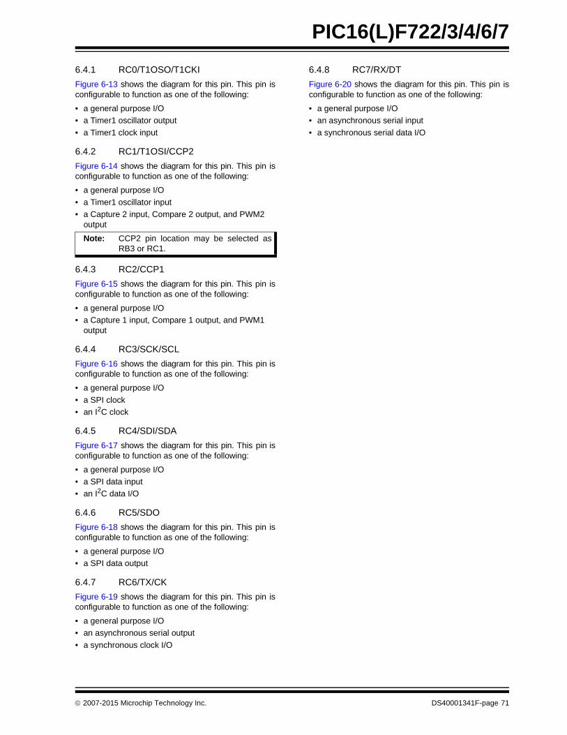
PIC16(L)F722/3/4/6/7
6.4.1 RC0/T1OSO/T1CKI
Figure 6-13 shows the diagram for this pin. This pin isconfigurable to function as one of the following:
• a general purpose I/O
• a Timer1 oscillator output
• a Timer1 clock input
6.4.2 RC1/T1OSI/CCP2
Figure 6-14 shows the diagram for this pin. This pin isconfigurable to function as one of the following:
• a general purpose I/O
• a Timer1 oscillator input
• a Capture 2 input, Compare 2 output, and PWM2 output
6.4.3 RC2/CCP1
Figure 6-15 shows the diagram for this pin. This pin isconfigurable to function as one of the following:
• a general purpose I/O
• a Capture 1 input, Compare 1 output, and PWM1 output
6.4.4 RC3/SCK/SCL
Figure 6-16 shows the diagram for this pin. This pin isconfigurable to function as one of the following:
• a general purpose I/O
• a SPI clock
• an I2C clock
6.4.5 RC4/SDI/SDA
Figure 6-17 shows the diagram for this pin. This pin isconfigurable to function as one of the following:
• a general purpose I/O
• a SPI data input
• an I2C data I/O
6.4.6 RC5/SDO
Figure 6-18 shows the diagram for this pin. This pin isconfigurable to function as one of the following:
• a general purpose I/O
• a SPI data output
6.4.7 RC6/TX/CK
Figure 6-19 shows the diagram for this pin. This pin isconfigurable to function as one of the following:
• a general purpose I/O
• an asynchronous serial output
• a synchronous clock I/O
6.4.8 RC7/RX/DT
Figure 6-20 shows the diagram for this pin. This pin isconfigurable to function as one of the following:
• a general purpose I/O
• an asynchronous serial input
• a synchronous serial data I/O
Note: CCP2 pin location may be selected asRB3 or RC1.
2007-2015 Microchip Technology Inc. DS40001341F-page 71

PIC16(L)F722/3/4/6/7
FIGURE 6-13: BLOCK DIAGRAM OF RC0
FIGURE 6-14: BLOCK DIAGRAM OF RC1
I/O Pin
VDD
VSS
D
QCK
Q
D
QCK
Q
RD
WR
WR
RD
T1OSCEN
Data Bus
PORTC
TRISC
TRISC
PORTC
To Timer1 CLK Input
OscillatorCircuit
RC1/T1OSI
0
1
I/O Pin
VDD
VSS
D
QCK
Q
D
QCK
Q
RD
WR
WR
RD
T1OSCEN
Data Bus
PORTC
TRISC
TRISC
PORTC
To CCP2(1) Input
CCP2OUT
CCP2OUTEnable
OscillatorCircuit
RC0/T1OSO
Note 1: CCP2 input is controlled by CCP2SEL in the APFCON register.
DS40001341F-page 72 2007-2015 Microchip Technology Inc.

PIC16(L)F722/3/4/6/7
FIGURE 6-15: BLOCK DIAGRAM OF RC2
FIGURE 6-16: BLOCK DIAGRAM OF RC3
0
1
I/O Pin
VDD
VSS
D
QCK
Q
D
QCK
Q
RD
WR
WR
RD
Data Bus
PORTC
TRISC
TRISC
PORTC
To CCP1 Input
CCP1OUT
CCP1OUTEnable
I/O Pin
VDD
VSS
D
QCK
Q
D
QCK
Q
RD
WR
WR
RD
Data Bus
PORTC
TRISC
TRISC
PORTC
To SSP SPI
0
1
SSPEN SSPM = I2C MODE
SCL
SSPEN
0
1SCK_MASTER
SSPM = SPI MODE
To SSP I2C
Clock Input
SCL Input
0
1
1
0
(2)
I2C(1)
Note 1: I2C Schmitt Trigger has special input levels.2: I2C Slew Rate limiting controlled by SMP bit of SSPSTAT register.
2007-2015 Microchip Technology Inc. DS40001341F-page 73

PIC16(L)F722/3/4/6/7
FIGURE 6-17: BLOCK DIAGRAM OF RC4
FIGURE 6-18: BLOCK DIAGRAM OF RC5
I/O Pin
VDD
VSS
D
QCK
Q
D
QCK
Q
RD
WR
WR
RD
Data Bus
PORTC
TRISC
TRISC
PORTC
To SSP SPI
0
1
SSPEN SSPM = I2C MODE
SDA FROM SSP
To SSP I2C
I2C(1)SDA Input
0
1
1
0
Data Input
(2)
Note 1: I2C Schmitt Trigger has special input levels.2: I2C Slew Rate limiting controlled by SMP bit of SSPSTAT register.
0
1
I/O Pin
VDD
VSS
D
QCK
Q
D
QCK
Q
RD
WR
WR
RD
Data Bus
PORTC
TRISC
TRISC
PORTC
SDO
SSPEN SSPM = SPI MODE
SDOEN
DS40001341F-page 74 2007-2015 Microchip Technology Inc.

PIC16(L)F722/3/4/6/7
FIGURE 6-19: BLOCK DIAGRAM OF RC6
FIGURE 6-20: BLOCK DIAGRAM OF RC7
I/O Pin
VDD
VSS
D
QCK
Q
D
QCK
Q
RD
WR
WR
RD
Data Bus
PORTC
TRISC
TRISC
PORTC
To USART
0
1
SPEN
0
1
USART_TX
SYNC
USART_CK
0
1
TXEN
SYNC
CSRC
Sync Clock Input
I/O Pin
VDD
VSS
D
QCK
Q
D
QCK
Q
RD
WR
WR
RD
Data Bus
PORTC
TRISC
TRISC
PORTC
To USART Data Input
0
1
SPENSYNC
USART_DT
SPENSYNCTXENSRENCREN
2007-2015 Microchip Technology Inc. DS40001341F-page 75

PIC16(L)F722/3/4/6/7
TABLE 6-3: SUMMARY OF REGISTERS ASSOCIATED WITH PORTC
Name Bit 7 Bit 6 Bit 5 Bit 4 Bit 3 Bit 2 Bit 1 Bit 0Value on
POR, BOR
Value on all other
Resets
APFCON — — — — — — SSSEL CCP2SEL ---- --00 ---- --00
CCP1CON — — DC1B1 DC1B0 CCP1M3 CCP1M2 CCP1M1 CCP1M0 --00 0000 --00 0000
CCP2CON — — DC2B1 DC2B0 CCP2M3 CCP2M2 CCP2M1 CCP2M0 --00 0000 --00 0000
PORTC RC7 RC6 RC5 RC4 RC3 RC2 RC1 RC0 xxxx xxxx xxxx xxxx
RCSTA SPEN RX9 SREN CREN ADDEN FERR OERR RX9D 0000 000x 0000 000x
SSPCON WCOL SSPOV SSPEN CKP SSPM3 SSPM2 SSPM1 SSPM0 0000 0000 0000 0000
SSPSTAT SMP CKE D/A P S R/W UA BF 0000 0000 0000 0000
T1CON TMR1CS1 TMR1CS0 T1CKPS1 T1CKPS0 T1OSCEN T1SYNC — TMR1ON 0000 00-0 uuuu uu-u
TXSTA CSRC TX9 TXEN SYNC — BRGH TRMT TX9D 0000 -010 0000 -010
TRISC TRISC7 TRISC6 TRISC5 TRISC4 TRISC3 TRISC2 TRISC1 TRISC0 1111 1111 1111 1111
Legend: x = unknown, u = unchanged, - = unimplemented locations read as ‘0’. Shaded cells are not used by Port C.
DS40001341F-page 76 2007-2015 Microchip Technology Inc.
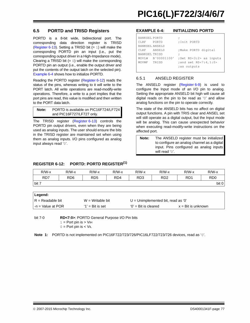
PIC16(L)F722/3/4/6/7
6.5 PORTD and TRISD Registers
PORTD is a 8-bit wide, bidirectional port. Thecorresponding data direction register is TRISD(Register 6-13). Setting a TRISD bit (= 1) will make thecorresponding PORTD pin an input (i.e., put thecorresponding output driver in a High-Impedance mode).Clearing a TRISD bit (= 0) will make the correspondingPORTD pin an output (i.e., enable the output driver andput the contents of the output latch on the selected pin).Example 6-4 shows how to initialize PORTD.
Reading the PORTD register (Register 6-12) reads thestatus of the pins, whereas writing to it will write to thePORT latch. All write operations are read-modify-writeoperations. Therefore, a write to a port implies that theport pins are read, this value is modified and then writtento the PORT data latch.
The TRISD register (Register 6-13) controls thePORTD pin output drivers, even when they are beingused as analog inputs. The user should ensure the bitsin the TRISD register are maintained set when usingthem as analog inputs. I/O pins configured as analoginput always read ‘0’.
EXAMPLE 6-4: INITIALIZING PORTD
6.5.1 ANSELD REGISTER
The ANSELD register (Register 6-9) is used toconfigure the Input mode of an I/O pin to analog.Setting the appropriate ANSELD bit high will cause alldigital reads on the pin to be read as ‘0’ and allowanalog functions on the pin to operate correctly.
The state of the ANSELD bits has no affect on digitaloutput functions. A pin with TRIS clear and ANSEL setwill still operate as a digital output, but the Input modewill be analog. This can cause unexpected behaviorwhen executing read-modify-write instructions on theaffected port.
Note: PORTD is available on PIC16F724/LF724and PIC16F727/LF727 only.
Note: The ANSELD register must be initializedto configure an analog channel as a digitalinput. Pins configured as analog inputswill read ‘0’.
BANKSEL PORTD ;CLRF PORTD ;Init PORTDBANKSEL ANSELDCLRF ANSELD ;Make PORTD digitalBANKSEL TRISD ;MOVLW B‘00001100’ ;Set RD<3:2> as inputsMOVWF TRISD ;and set RD<7:4,1:0>
;as outputs
REGISTER 6-12: PORTD: PORTD REGISTER(1)
R/W-x R/W-x R/W-x R/W-x R/W-x R/W-x R/W-x R/W-x
RD7 RD6 RD5 RD4 RD3 RD2 RD1 RD0
bit 7 bit 0
Legend:
R = Readable bit W = Writable bit U = Unimplemented bit, read as ‘0’
-n = Value at POR ‘1’ = Bit is set ‘0’ = Bit is cleared x = Bit is unknown
bit 7-0 RD<7:0>: PORTD General Purpose I/O Pin bits1 = Port pin is > VIH
0 = Port pin is < VIL
Note 1: PORTD is not implemented on PIC16F722/723/726/PIC16LF722/723/726 devices, read as ‘0’.
2007-2015 Microchip Technology Inc. DS40001341F-page 77

PIC16(L)F722/3/4/6/7
6.5.2 RD0/CPS8
Figure 6-21 shows the diagram for these pins. They areconfigurable to function as one of the following:
• a general purpose I/O
• a capacitive sensing input
6.5.3 RD1/CPS9
Figure 6-21 shows the diagram for these pins. They areconfigurable to function as one of the following:
• a general purpose I/O
• a capacitive sensing input
6.5.4 RD2/CPS10
Figure 6-21 shows the diagram for these pins. They areconfigurable to function as one of the following:
• a general purpose I/O
• a capacitive sensing input
6.5.5 RD3/CPS11
Figure 6-21 shows the diagram for these pins. They areconfigurable to function as one of the following:
• a general purpose I/O
• a capacitive sensing input
REGISTER 6-13: TRISD: PORTD TRI-STATE REGISTER(1)
R/W-1 R/W-1 R/W-1 R/W-1 R/W-1 R/W-1 R/W-1 R/W-1
TRISD7 TRISD6 TRISD5 TRISD4 TRISD3 TRISD2 TRISD1 TRISD0
bit 7 bit 0
Legend:
R = Readable bit W = Writable bit U = Unimplemented bit, read as ‘0’
-n = Value at POR ‘1’ = Bit is set ‘0’ = Bit is cleared x = Bit is unknown
bit 7-0 TRISD<7:0>: PORTD Tri-State Control bits1 = PORTD pin configured as an input (tri-stated)0 = PORTD pin configured as an output
Note 1: TRISD is not implemented on PIC16F722/723/726/PIC16LF722/723/726 devices, read as ‘0’.
REGISTER 6-14: ANSELD: PORTD ANALOG SELECT REGISTER(2)
R/W-1 R/W-1 R/W-1 R/W-1 R/W-1 R/W-1 R/W-1 R/W-1
ANSD7 ANSD6 ANSD5 ANSD4 ANSD3 ANSD2 ANSD1 ANSD0
bit 7 bit 0
Legend:
R = Readable bit W = Writable bit U = Unimplemented bit, read as ‘0’
-n = Value at POR ‘1’ = Bit is set ‘0’ = Bit is cleared x = Bit is unknown
bit 7-0 ANSD<7:0>: Analog Select between Analog or Digital Function on Pins RD<7:0>, respectively
0 = Digital I/O. Pin is assigned to port or Digital special function.1 = Analog input. Pin is assigned as analog input(1). Digital Input buffer disabled.
Note 1: When setting a pin to an analog input, the corresponding TRIS bit must be set to Input mode in order to allow external control of the voltage on the pin.
2: ANSELD register is not implemented on the PIC16F722/723/726/PIC16LF722/723/726. Read as ‘0’.
Note: PORTD is available on PIC16F724/LF724and PIC16F727/LF727 only.
DS40001341F-page 78 2007-2015 Microchip Technology Inc.

PIC16(L)F722/3/4/6/7
6.5.6 RD4/CPS12
Figure 6-21 shows the diagram for these pins. They areconfigurable to function as one of the following:
• a general purpose I/O
• a capacitive sensing input
6.5.7 RD5/CPS13
Figure 6-21 shows the diagram for these pins. They areconfigurable to function as one of the following:
• a general purpose I/O
• a capacitive sensing input
6.5.8 RD6/CPS14
Figure 6-21 shows the diagram for these pins. They areconfigurable to function as one of the following:
• a general purpose I/O
• a capacitive sensing input
6.5.9 RD7/CPS15
Figure 6-21 shows the diagram for these pins. They areconfigurable to function as one of the following:
• a general purpose I/O
• a capacitive sensing input
FIGURE 6-21: BLOCK DIAGRAM OF RD<7:0>
TABLE 6-4: SUMMARY OF REGISTERS ASSOCIATED WITH PORTD(1)
Name Bit 7 Bit 6 Bit 5 Bit 4 Bit 3 Bit 2 Bit 1 Bit 0Value on
POR, BOR
Value on all other Resets
ANSELD ANSD7 ANSD6 ANSD5 ANSD4 ANSD3 ANSD2 ANSD1 ANSD0 1111 1111 1111 1111
CPSCON0 CPSON — — — CPSRNG1 CPSRNG0 CPSOUT T0XCS 0--- 0000 0--- 0000
CPSCON1 — — — — CPSCH3 CPSCH2 CPSCH1 CPSCH0 ---- 0000 ---- 0000
PORTD RD7 RD6 RD5 RD4 RD3 RD2 RD1 RD0 xxxx xxxx xxxx xxxx
TRISD TRISD7 TRISD6 TRISD5 TRISD4 TRISD3 TRISD2 TRISD1 TRISD0 1111 1111 1111 1111
Legend: x = unknown, u = unchanged, – = unimplemented locations read as ‘0’. Shaded cells are not used by PORTD.Note 1: These registers are not implemented on the PIC16F722/723/726/PIC16LF722/723/726 devices, read as ‘0’.
I/O Pin
VDD
VSS
D
QCK
Q
D
QCK
Q
RD
WR
WR
RD
ANSD<7:0>
Data Bus
PORTD
TRISD
TRISD
PORTD
Note: PORTD is available on PIC16F724/LF724 and PIC16F727/LF727 only.
To Cap Sensor
2007-2015 Microchip Technology Inc. DS40001341F-page 79
PIC16(L)F722/3/4/6/7
6.6 PORTE and TRISE Registers
PORTE is a 4-bit wide, bidirectional port. Thecorresponding data direction register is TRISE. Setting aTRISE bit (= 1) will make the corresponding PORTE pinan input (i.e., put the corresponding output driver in aHigh-Impedance mode). Clearing a TRISE bit (= 0) willmake the corresponding PORTE pin an output (i.e.,enable the output driver and put the contents of theoutput latch on the selected pin). The exception is RE3,which is input only and its TRIS bit will always read as‘1’. Example 6-5 shows how to initialize PORTE.
Reading the PORTE register (Register 6-15) reads thestatus of the pins, whereas writing to it will write to thePORT latch. All write operations are read-modify-writeoperations. Therefore, a write to a port implies that theport pins are read, this value is modified and thenwritten to the PORT data latch. RE3 reads ‘0’ whenMCLRE = 1.
The TRISE register (Register 6-16) controls the PORTEpin output drivers, even when they are being used asanalog inputs. The user should ensure the bits in theTRISE register are maintained set when using them asanalog inputs. I/O pins configured as analog input alwaysread ‘0’.
EXAMPLE 6-5: INITIALIZING PORTE
Note: RE<2:0> and TRISE<2:0> are notimplemented on the PIC16F722/723/726/PIC16LF722/723/726. Read as ‘0’.
Note: The ANSELE register must be initializedto configure an analog channel as a digitalinput. Pins configured as analog inputswill read ‘0’.
BANKSEL PORTE ;CLRF PORTE ;Init PORTEBANKSEL ANSELE ;CLRF ANSELE ;digital I/OBANKSEL TRISE ;MOVLW B‘00001100’ ;Set RE<2> as an inputMOVWF TRISE ;and set RE<1:0>
;as outputs
DS40001341F-page 80 2007-2015 Microchip Technology Inc.

PIC16(L)F722/3/4/6/7
REGISTER 6-15: PORTE: PORTE REGISTER
U-0 U-0 U-0 U-0 R-x R/W-x R/W-x R/W-x
— — — — RE3 RE2(1) RE1(1) RE0(1)
bit 7 bit 0
Legend:
R = Readable bit W = Writable bit U = Unimplemented bit, read as ‘0’
-n = Value at POR ‘1’ = Bit is set ‘0’ = Bit is cleared x = Bit is unknown
bit 7-4 Unimplemented: Read as ‘0’
bit 3-0 RE<3:0>: PORTE I/O Pin bits(1)
1 = Port pin is > VIH
0 = Port pin is < VIL
Note 1: RE<2:0> are not implemented on the PIC16F722/723/726/PIC16LF722/723/726. Read as ‘0’.
REGISTER 6-16: TRISE: PORTE TRI-STATE REGISTER
U-0 U-0 U-0 U-0 R-1 R/W-1 R/W-1 R/W-1
— — — — TRISE3 TRISE2(1) TRISE1(1) TRISE0(1)
bit 7 bit 0
Legend:
R = Readable bit W = Writable bit U = Unimplemented bit, read as ‘0’
-n = Value at POR ‘1’ = Bit is set ‘0’ = Bit is cleared x = Bit is unknown
bit 7-4 Unimplemented: Read as ‘0’
bit 3 TRISE3: RE3 Port Tri-state Control bit
This bit is always ‘1’ as RE3 is an input only
bit 2-0 TRISE<2:0>: RE<2:0> Tri-State Control bits(1)
1 = PORTE pin configured as an input (tri-stated)0 = PORTE pin configured as an output
Note 1: TRISE<2:0> are not implemented on the PIC16F722/723/726/PIC16LF722/723/726. Read as ‘0’.
2007-2015 Microchip Technology Inc. DS40001341F-page 81

PIC16(L)F722/3/4/6/7
TABLE 6-5: SUMMARY OF REGISTERS ASSOCIATED WITH PORTE
REGISTER 6-17: ANSELE: PORTE ANALOG SELECT REGISTER
U-0 U-0 U-0 U-0 U-0 R/W-1 R/W-1 R/W-1
— — — — — ANSE2(2) ANSE1(2) ANSE0(2)
bit 7 bit 0
Legend:
R = Readable bit W = Writable bit U = Unimplemented bit, read as ‘0’
-n = Value at POR ‘1’ = Bit is set ‘0’ = Bit is cleared x = Bit is unknown
bit 7-3 Unimplemented: Read as ‘0’
bit 2-0 ANSE<2:0>: Analog Select between Analog or Digital Function on Pins RE<2:0>, respectively
0 = Digital I/O. Pin is assigned to port or Digital special function.1 = Analog input. Pin is assigned as analog input(1). Digital Input buffer disabled.
Note 1: When setting a pin to an analog input, the corresponding TRIS bit must be set to Input mode in order to allow external control of the voltage on the pin.
2: ANSELE register is not implemented on the PIC16F722/723/726/PIC16LF722/723/726. Read as ‘0’
Name Bit 7 Bit 6 Bit 5 Bit 4 Bit 3 Bit 2 Bit 1 Bit 0Value on
POR, BOR
Value on all other Resets
ADCON0 — — CHS3 CHS2 CHS1 CHS0 GO/DONE ADON --00 0000 --00 0000
ANSELE — — — — — ANSE2 ANSE1 ANSE0 ---- -111 ---- -111
PORTE — — — — RE3 RE2 RE1 RE0 ---- xxxx ---- xxxx
TRISE — — — — TRISE3(2) TRISE2(1) TRISE1(1) TRISE0(1) ---- 1111 ---- 1111
Legend: x = unknown, u = unchanged, – = unimplemented locations read as ‘0’. Shaded cells are not used by PORTENote 1: These registers are not implemented on the PIC16F722/723/726/PIC16LF722/723/726 devices, read as ‘0’.
2: This bit is always ‘1’ as RE3 is input only.
DS40001341F-page 82 2007-2015 Microchip Technology Inc.

PIC16(L)F722/3/4/6/7
6.6.1 RE0/AN5(1)
Figure 6-22 shows the diagram for this pin. This pin isconfigurable to function as one of the following:
• a general purpose I/O
• an analog input for the ADC
6.6.2 RE1/AN6(1)
Figure 6-22 shows the diagram for this pin. This pin isconfigurable to function as one of the following:
• a general purpose I/O
• an analog input for the ADC
6.6.3 RE2/AN7(1)
Figure 6-22 shows the diagram for this pin. This pin isconfigurable to function as one of the following:
• a general purpose I/O
• an analog input for the ADC
6.6.4 RE3/MCLR/VPP
Figure 6-23 shows the diagram for this pin. This pin isconfigurable to function as one of the following:
• a general purpose input
• as Master Clear Reset with weak pull-up
• a programming voltage reference input
Note 1: RE0/AN5 is available on PIC16F724/LF724 and PIC16F727/LF727 only.
Note 1: RE0/AN5 is available on PIC16F724/LF724 and PIC16F727/LF727 only.
Note 1: RE0/AN5 is available on PIC16F724/LF724 and PIC16F727/LF727 only.
2007-2015 Microchip Technology Inc. DS40001341F-page 83

PIC16(L)F722/3/4/6/7
FIGURE 6-22: BLOCK DIAGRAM OF RE<2:0>
FIGURE 6-23: BLOCK DIAGRAM OF RE3
I/O Pin
VDD
VSS
D
QCK
Q
D
QCK
Q
RD
WR
WR
RD
To A/D Converter
ANSE<0:2>
Data Bus
PORTE
TRISE
TRISE
PORTE
Note: RE<2:0> are not implemented on PIC16F722/723/726/PIC16LF722/723/726.
I/O Pin
VSS
RD
RD
Data Bus
TRISE
PORTE
VSS
High-VoltageDetect
In-Circuit Serial Programming™ mode
Pulse FilterMCLRMCLR Circuit
Power for Programming Flash
VDD
WeakICSP™ Mode Detect
DS40001341F-page 84 2007-2015 Microchip Technology Inc.

PIC16(L)F722/3/4/6/7
7.0 OSCILLATOR MODULE
7.1 Overview
The oscillator module has a wide variety of clock sourcesand selection features that allow it to be used in a widerange of applications while maximizing performance andminimizing power consumption. Figure 7-1 illustrates ablock diagram of the oscillator module.
Clock sources can be configured from externaloscillators, quartz crystal resonators, ceramic resonatorsand Resistor-Capacitor (RC) circuits. In addition, thesystem can be configured to use an internal calibratedhigh-frequency oscillator as clock source, with a choiceof selectable speeds via software.
Clock source modes are configured by the FOSC bitsin Configuration Word 1 (CONFIG1). The oscillatormodule can be configured for one of eight modes ofoperation.
1. RC – External Resistor-Capacitor (RC) withFOSC/4 output on OSC2/CLKOUT.
2. RCIO – External Resistor-Capacitor (RC) withI/O on OSC2/CLKOUT.
3. INTOSC – Internal oscillator with FOSC/4 outputon OSC2 and I/O on OSC1/CLKIN.
4. INTOSCIO – Internal oscillator with I/O onOSC1/CLKIN and OSC2/CLKOUT.
5. EC – External clock with I/O on OSC2/CLKOUT.
6. HS – High Gain Crystal or Ceramic Resonatormode.
7. XT – Medium Gain Crystal or CeramicResonator Oscillator mode.
8. LP – Low-Power Crystal mode.
FIGURE 7-1: SIMPLIFIED PIC® MCU CLOCK SOURCE BLOCK DIAGRAM
(CPU and Peripherals)
OSC1
OSC2
Sleep
External Oscillator
LP, XT, HS, RC, EC
System Clock
Pos
tsca
ler
MU
X
MU
X
16 MHz/500 kHz
8 MHz/250 kHz
4 MHz/125 kHz
2 MHz/62.5 kHz
IRCF<1:0>
11
10
01
00
FOSC<2:0>(Configuration Word 1)
Internal Oscillator(OSCCON Register)
500 kHzINTOSC
32x
MU
X
0
1PLL
PLLEN(Configuration Word 1)
2007-2015 Microchip Technology Inc. DS40001341F-page 85
PIC16(L)F722/3/4/6/7
7.2 Clock Source Modes
Clock source modes can be classified as external orinternal.
• Internal clock source (INTOSC) is contained within the oscillator module and derived from a 500 kHz high precision oscillator. The oscillator module has eight selectable output frequencies, with a maximum internal frequency of 16 MHz.
• External clock modes rely on external circuitry for the clock source. Examples are: oscillator modules (EC mode), quartz crystal resonators or ceramic resonators (LP, XT and HS modes) and Resistor-Capacitor (RC) mode circuits.
The system clock can be selected between external orinternal clock sources via the FOSC bits of theConfiguration Word 1.
7.3 Internal Clock Modes
The oscillator module has eight output frequenciesderived from a 500 kHz high precision oscillator. TheIRCF bits of the OSCCON register select thepostscaler applied to the clock source dividing thefrequency by 1, 2, 4 or 8. Setting the PLLEN bit of theConfiguration Word 1 locks the internal clock source to16 MHz before the postscaler is selected by the IRCFbits. The PLLEN bit must be set or cleared at the timeof programming; therefore, only the upper or low fourclock source frequencies are selectable in software.
7.3.1 INTOSC AND INTOSCIO MODES
The INTOSC and INTOSCIO modes configure theinternal oscillators as the system clock source whenthe device is programmed using the oscillator selectionor the FOSC<2:0> bits in the CONFIG1 register. SeeSection 8.0 “Device Configuration” for moreinformation.
In INTOSC mode, OSC1/CLKIN is available for generalpurpose I/O. OSC2/CLKOUT outputs the selectedinternal oscillator frequency divided by 4. The CLKOUTsignal may be used to provide a clock for externalcircuitry, synchronization, calibration, test or otherapplication requirements.
In INTOSCIO mode, OSC1/CLKIN andOSC2/CLKOUT are available for general purpose I/O.
7.3.2 FREQUENCY SELECT BITS (IRCF)
The output of the 500 kHz INTOSC and 16 MHzINTOSC, with Phase-Locked Loop enabled, connect toa postscaler and multiplexer (see Figure 7-1). TheInternal Oscillator Frequency Select bits (IRCF) of theOSCCON register select the frequency output of theinternal oscillator. Depending upon the PLLEN bit, oneof four frequencies of two frequency sets can beselected via software:
If PLLEN = 1, frequency selection is as follows:
• 16 MHz
• 8 MHz (default after Reset)
• 4 MHz
• 2 MHz
If PLLEN = 0, frequency selection is as follows:
• 500 kHz
• 250 kHz (default after Reset)
• 125 kHz
• 62.5 kHz
There is no start-up delay before a new frequencyselected in the IRCF bits takes effect. This is becausethe old and new frequencies are derived from INTOSCvia the postscaler and multiplexer.
Start-up delay specifications are located in theTable 23-2 in Section 23.0 “ElectricalSpecifications”.
Note: Following any Reset, the IRCF<1:0> bitsof the OSCCON register are set to ‘10’ andthe frequency selection is set to 8 MHz or250 kHz. The user can modify the IRCFbits to select a different frequency.
DS40001341F-page 86 2007-2015 Microchip Technology Inc.

PIC16(L)F722/3/4/6/7
7.4 Oscillator Control
The Oscillator Control (OSCCON) register (Figure 7-1)displays the status and allows frequency selection of theinternal oscillator (INTOSC) system clock. TheOSCCON register contains the following bits:
• Frequency selection bits (IRCF)
• Status Locked bits (ICSL)
• Status Stable bits (ICSS)
REGISTER 7-1: OSCCON: OSCILLATOR CONTROL REGISTER
U-0 U-0 R/W-1 R/W-0 R-q R-q U-0 U-0
— — IRCF1 IRCF0 ICSL ICSS — —
bit 7 bit 0
Legend:
R = Readable bit W = Writable bit U = Unimplemented bit, read as ‘0’
-n = Value at POR ‘1’ = Bit is set ‘0’ = Bit is cleared x = Bit is unknown
q = Value depends on condition
bit 7-6 Unimplemented: Read as ‘0’
bit 5-4 IRCF<1:0>: Internal Oscillator Frequency Select bitsWhen PLLEN = 1 (16 MHz INTOSC)11 = 16 MHz 10 = 8 MHz (POR value)01 = 4 MHz00 = 2 MHzWhen PLLEN = 0 (500 kHz INTOSC)11 = 500 kHz 10 = 250 kHz (POR value)01 = 125 kHz00 = 62.5 kHz
bit 3 ICSL: Internal Clock Oscillator Status Locked bit (2% Stable)
1 = 16 MHz/500 kHz Internal Oscillator (HFIOSC) is in lock0 = 16 MHz/500 kHz Internal Oscillator (HFIOSC) has not yet locked
bit 2 ICSS: Internal Clock Oscillator Status Stable bit (0.5% Stable)
1 = 16 MHz/500 kHz Internal Oscillator (HFIOSC) has stabilized to its maximum accuracy0 = 16 MHz/500 kHz Internal Oscillator (HFIOSC) has not yet reached its maximum accuracy
bit 1-0 Unimplemented: Read as ‘0’
2007-2015 Microchip Technology Inc. DS40001341F-page 87

PIC16(L)F722/3/4/6/7
7.5 Oscillator Tuning
The INTOSC is factory calibrated but can be adjustedin software by writing to the OSCTUNE register(Register 7-2).
The default value of the OSCTUNE register is ‘0’. Thevalue is a 6-bit two’s complement number.
When the OSCTUNE register is modified, the INTOSCfrequency will begin shifting to the new frequency. Codeexecution continues during this shift. There is noindication that the shift has occurred.
REGISTER 7-2: OSCTUNE: OSCILLATOR TUNING REGISTER
U-0 U-0 R/W-0 R/W-0 R/W-0 R/W-0 R/W-0 R/W-0
— — TUN5 TUN4 TUN3 TUN2 TUN1 TUN0
bit 7 bit 0
Legend:
R = Readable bit W = Writable bit U = Unimplemented bit, read as ‘0’
-n = Value at POR ‘1’ = Bit is set ‘0’ = Bit is cleared x = Bit is unknown
bit 7-6 Unimplemented: Read as ‘0’
bit 5-0 TUN<5:0>: Frequency Tuning bits01 1111 = Maximum frequency01 1110 = •••00 0001 = 00 0000 = Oscillator module is running at the factory-calibrated frequency.11 1111 = •••10 0000 = Minimum frequency
DS40001341F-page 88 2007-2015 Microchip Technology Inc.

PIC16(L)F722/3/4/6/7
7.6 External Clock Modes
7.6.1 OSCILLATOR START-UP TIMER (OST)
If the oscillator module is configured for LP, XT or HSmodes, the Oscillator Start-up Timer (OST) counts1024 oscillations on the OSC1 pin before the device isreleased from Reset. This occurs following a Power-onReset (POR) and when the Power-up Timer (PWRT)has expired (if configured), or a wake-up from Sleep.During this time, the program counter does notincrement and program execution is suspended. TheOST ensures that the oscillator circuit, using a quartzcrystal resonator or ceramic resonator, has started andis providing a stable system clock to the oscillatormodule.
7.6.2 EC MODE
The External Clock (EC) mode allows an externallygenerated logic level as the system clock source. Whenoperating in this mode, an external clock source isconnected to the OSC1 input and the OSC2 is availablefor general purpose I/O. Figure 7-2 shows the pinconnections for EC mode.
The Oscillator Start-up Timer (OST) is disabled whenEC mode is selected. Therefore, there is no delay inoperation after a Power-on Reset (POR) or wake-upfrom Sleep. Because the PIC® MCU design is fullystatic, stopping the external clock input will have theeffect of halting the device while leaving all data intact.Upon restarting the external clock, the device willresume operation as if no time had elapsed.
FIGURE 7-2: EXTERNAL CLOCK (EC) MODE OPERATION
7.6.3 LP, XT, HS MODES
The LP, XT and HS modes support the use of quartzcrystal resonators or ceramic resonators connected toOSC1 and OSC2 (Figure 7-3). The mode selects a low,medium or high gain setting of the internalinverter-amplifier to support various resonator typesand speed.
LP Oscillator mode selects the lowest gain setting of theinternal inverter-amplifier. LP mode current consumptionis the least of the three modes. This mode is best suitedto drive resonators with a low drive level specification, forexample, tuning fork type crystals.
XT Oscillator mode selects the intermediate gainsetting of the internal inverter-amplifier. XT modecurrent consumption is the medium of the three modes.This mode is best suited to drive resonators with amedium drive level specification.
HS Oscillator mode selects the highest gain setting of theinternal inverter-amplifier. HS mode current consumptionis the highest of the three modes. This mode is bestsuited for resonators that require a high drive setting.
Figure 7-3 and Figure 7-4 show typical circuits forquartz crystal and ceramic resonators, respectively.
FIGURE 7-3: QUARTZ CRYSTAL OPERATION (LP, XT OR HS MODE)
OSC1/CLKIN
OSC2/CLKOUT(1)I/O
Clock fromExt. System
PIC® MCU
Note 1: Alternate pin functions are described in Section 6.1 “Alternate Pin Function”.
Note 1: Quartz crystal characteristics varyaccording to type, package andmanufacturer. The user should consult themanufacturer data sheets for specificationsand recommended application.
2: Always verify oscillator performance overthe VDD and temperature range that isexpected for the application.
3: For oscillator design assistance, referencethe following Microchip Applications Notes:
• AN826, Crystal Oscillator Basics and Crystal Selection for rfPIC® and PIC® Devices (DS00826)
• AN849, Basic PIC® Oscillator Design (DS00849)
• AN943, Practical PIC® Oscillator Analysis and Design (DS00943)
• AN949, Making Your Oscillator Work (DS00949).
Note 1: A series resistor (RS) may be required forquartz crystals with low drive level.
2: The value of RF varies with the Oscillator modeselected.
C1
C2
Quartz
RS(1)
OSC1/CLKIN
RF(2) Sleep
To Internal Logic
PIC® MCU
Crystal
OSC2/CLKOUT
2007-2015 Microchip Technology Inc. DS40001341F-page 89

PIC16(L)F722/3/4/6/7
FIGURE 7-4: CERAMIC RESONATOR OPERATION(XT OR HS MODE)
7.6.4 EXTERNAL RC MODES
The external Resistor-Capacitor (RC) modes supportthe use of an external RC circuit. This allows thedesigner maximum flexibility in frequency choice whilekeeping costs to a minimum when clock accuracy is notrequired. There are two modes: RC and RCIO.
In RC mode, the RC circuit connects to OSC1.OSC2/CLKOUT outputs the RC oscillator frequencydivided by 4. This signal may be used to provide a clockfor external circuitry, synchronization, calibration, testor other application requirements. Figure 7-5 showsthe external RC mode connections.
FIGURE 7-5: EXTERNAL RC MODES
In RCIO mode, the RC circuit is connected to OSC1.OSC2 becomes an additional general purpose I/O pin.
The RC oscillator frequency is a function of the supplyvoltage, the resistor (REXT) and capacitor (CEXT) valuesand the operating temperature. Other factors affectingthe oscillator frequency are:
• threshold voltage variation• component tolerances• packaging variations in capacitance
The user also needs to take into account variation dueto tolerance of external RC components used.
TABLE 7-1: SUMMARY OF REGISTERS ASSOCIATED WITH CLOCK SOURCES
Note 1: A series resistor (RS) may be required forceramic resonators with low drive level.
2: The value of RF varies with the Oscillator modeselected.
3: An additional parallel feedback resistor (RP)may be required for proper ceramic resonatoroperation.
C1
C2 Ceramic RS(1)
OSC1/CLKIN
RF(2) Sleep
To Internal Logic
PIC® MCU
RP(3)
Resonator
OSC2/CLKOUT
OSC2/CLKOUT(1)
CEXT
REXT
PIC® MCU
OSC1/CLKIN
FOSC/4 or
InternalClock
VDD
VSS
Recommended values: 10 k REXT 100 k, <3V3 k REXT 100 k, 3-5VCEXT > 20 pF, 2-5V
Note 1: Alternate pin functions are described in Section 6.1 “Alternate Pin Function”.
2: Output depends upon RC or RCIO clock mode.
I/O(2)
Name Bit 7 Bit 6 Bit 5 Bit 4 Bit 3 Bit 2 Bit 1 Bit 0Value on
POR, BOR
Value on all other Resets(1)
CONFIG1(1) — CP MCLRE PWRTE WDTE FOSC2 FOSC1 FOSC0 — —
OSCCON — — IRCF1 IRCF0 ICSL ICSS — — --10 qq-- --10 qq--
OSCTUNE — — TUN5 TUN4 TUN3 TUN2 TUN1 TUN0 --00 0000 --uu uuuu
Legend: x = unknown, u = unchanged, – = unimplemented locations read as ‘0’. Shaded cells are not used by clock sources.Note 1: See Configuration Word 1 (Register 8-1) for operation of all bits.
DS40001341F-page 90 2007-2015 Microchip Technology Inc.
PIC16(L)F722/3/4/6/7
8.0 DEVICE CONFIGURATION
Device Configuration consists of Configuration Word 1and Configuration Word 2 registers, Code Protectionand Device ID.
8.1 Configuration Words
There are several Configuration Word bits that allowdifferent oscillator and memory protection options.These are implemented as Configuration Word 1register at 2007h and Configuration Word 2 register at2008h. These registers are only accessible duringprogramming.
REGISTER 8-1: CONFIG1: CONFIGURATION WORD REGISTER 1
R/P-1 R/P-1 U-1(4) R/P-1 R/P-1 R/P-1
— — DEBUG PLLEN — BORV BOREN1 BOREN0
bit 15 bit 8
U-1(4) R/P-1 R/P-1 R/P-1 R/P-1 R/P-1 R/P-1 R/P-1
— CP MCLRE PWRTE WDTE FOSC2 FOSC1 FOSC0
bit 7 bit 0
Legend: P = Programmable bit
R = Readable bit W = Writable bit U = Unimplemented bit, read as ‘0’
-n = Value at POR ‘1’ = Bit is set ‘0’ = Bit is cleared x = Bit is unknown
bit 13 DEBUG: In-Circuit Debugger Mode bit1 = In-Circuit Debugger disabled, RB6/ICSPCLK and RB7/ICSPDAT are general purpose I/O pins0 = In-Circuit Debugger enabled, RB6/ICSPCLK and RB7/ICSPDAT are dedicated to the debugger
bit 12 PLLEN: INTOSC PLL Enable bit0 = INTOSC Frequency is 500 kHz1 = INTOSC Frequency is 16 MHz (32x)
bit 11 Unimplemented: Read as ‘1’
bit 10 BORV: Brown-out Reset Voltage selection bit0 = Brown-out Reset Voltage (VBOR) set to 2.5 V nominal1 = Brown-out Reset Voltage (VBOR) set to 1.9 V nominal
bit 9-8 BOREN<1:0>: Brown-out Reset Selection bits(1)
0x = BOR disabled (Preconditioned State)10 = BOR enabled during operation and disabled in Sleep11 = BOR enabled
bit 7 Unimplemented: Read as ‘1’
bit 6 CP: Code Protection bit(2)
1 = Program memory code protection is disabled0 = Program memory code protection is enabled
bit 5 MCLRE: RE3/MCLR pin function select bit(3)
1 = RE3/MCLR pin function is MCLR0 = RE3/MCLR pin function is digital input, MCLR internally tied to VDD
Note 1: Enabling Brown-out Reset does not automatically enable Power-up Timer.2: The entire program memory will be erased when the code protection is turned off.3: When MCLR is asserted in INTOSC or RC mode, the internal clock oscillator is disabled.4: MPLAB® X IDE masks unimplemented Configuration bits to ‘0’.
2007-2015 Microchip Technology Inc. DS40001341F-page 91

PIC16(L)F722/3/4/6/7
bit 4 PWRTE: Power-up Timer Enable bit1 = PWRT disabled0 = PWRT enabled
bit 3 WDTE: Watchdog Timer Enable bit1 = WDT enabled0 = WDT disabled
bit 2-0 FOSC<2:0>: Oscillator Selection bits111 = RC oscillator: CLKOUT function on RA6/OSC2/CLKOUT pin, RC on RA7/OSC1/CLKIN110 = RCIO oscillator: I/O function on RA6/OSC2/CLKOUT pin, RC on RA7/OSC1/CLKIN101 = INTOSC oscillator: CLKOUT function on RA6/OSC2/CLKOUT pin, I/O function on
RA7/OSC1/CLKIN100 = INTOSCIO oscillator: I/O function on RA6/OSC2/CLKOUT pin, I/O function on
RA7/OSC1/CLKIN011 = EC: I/O function on RA6/OSC2/CLKOUT pin, CLKIN on RA7/OSC1/CLKIN010 = HS oscillator: High-speed crystal/resonator on RA6/OSC2/CLKOUT and RA7/OSC1/CLKIN001 = XT oscillator: Crystal/resonator on RA6/OSC2/CLKOUT and RA7/OSC1/CLKIN000 = LP oscillator: Low-power crystal on RA6/OSC2/CLKOUT and RA7/OSC1/CLKIN
REGISTER 8-1: CONFIG1: CONFIGURATION WORD REGISTER 1 (CONTINUED)
Note 1: Enabling Brown-out Reset does not automatically enable Power-up Timer.2: The entire program memory will be erased when the code protection is turned off.3: When MCLR is asserted in INTOSC or RC mode, the internal clock oscillator is disabled.4: MPLAB® X IDE masks unimplemented Configuration bits to ‘0’.
REGISTER 8-2: CONFIG2: CONFIGURATION WORD REGISTER 2
U-1(1) U-1(1) U-1(1) U-1(1) U-1(1) U-1(1)
— — — — — — — —
bit 15 bit 8
U-1(1) U-1(1) R/P-1 R/P-1 U-1(1) U-1(1) U-1(1) U-1(1)
— — VCAPEN1 VCAPEN0 — — — —
bit 7 bit 0
Legend: P = Programmable bit
R = Readable bit W = Writable bit U = Unimplemented bit, read as ‘0’
-n = Value at POR ‘1’ = Bit is set ‘0’ = Bit is cleared x = Bit is unknown
bit 13-6 Unimplemented: Read as ‘1’
bit 5-4 VCAPEN<1:0>: Voltage Regulator Capacitor Enable bitsFor the PIC16LF72X:These bits are ignored. All VCAP pin functions are disabled.For the PIC16F72X:00 = VCAP functionality is enabled on RA001 = VCAP functionality is enabled on RA510 = VCAP functionality is enabled on RA611 = All VCAP functions are disabled (not recommended)
bit 3-0 Unimplemented: Read as ‘1’
Note 1: MPLAB® X IDE masks unimplemented Configuration bits to ‘0’.
DS40001341F-page 92 2007-2015 Microchip Technology Inc.

PIC16(L)F722/3/4/6/7
8.2 Code Protection
If the code protection bit(s) have not beenprogrammed, the on-chip program memory can beread out using ICSP™ for verification purposes.
8.3 User ID
Four memory locations (2000h-2003h) are designatedas ID locations where the user can store checksum orother code identification numbers. These locations arenot accessible during normal execution, but are read-able and writable during Program/Verify mode. Onlythe Least Significant seven bits of the ID locations arereported when using MPLAB IDE. See the“PIC16(L)F72X Memory Programming Specification”(DS41332) for more information.
Note: The entire Flash program memory will beerased when the code protection is turnedoff. See the “PIC16(L)F72X MemoryProgramming Specification” (DS41332)for more information.
2007-2015 Microchip Technology Inc. DS40001341F-page 93

PIC16(L)F722/3/4/6/7
9.0 ANALOG-TO-DIGITAL CONVERTER (ADC) MODULE
The Analog-to-Digital Converter (ADC) allowsconversion of an analog input signal to a 8-bit binaryrepresentation of that signal. This device uses analoginputs, which are multiplexed into a single sample andhold circuit. The output of the sample and hold isconnected to the input of the converter. The convertergenerates a 8-bit binary result via successiveapproximation and stores the conversion result into theADC result register (ADRES). Figure 9-1 shows theblock diagram of the ADC.
The ADC voltage reference is software selectable to beeither internally generated or externally supplied.
The ADC can generate an interrupt upon completion ofa conversion. This interrupt can be used to wake-up thedevice from Sleep.
FIGURE 9-1: ADC BLOCK DIAGRAM
AN0
AN1
AN2
AN4
AVDD
VREF+
ADON
GO/DONE
ADREF = 10
ADREF = 0x
CHS<3:0>
VSS
AN5
AN6
AN7
AN3
AN8
AN9
AN10
AN11
AN12
AN13
Reserved
FVREF
0000
0001
0010
0011
0100
0101
0111
0110
1000
1001
1010
1011
1100
1101
1110
1111
8
ADC
ADRES
ADREF = 11
DS40001341F-page 94 2007-2015 Microchip Technology Inc.

PIC16(L)F722/3/4/6/7
9.1 ADC Configuration
When configuring and using the ADC, the followingfunctions must be considered:
• Port configuration
• Channel selection
• ADC voltage reference selection
• ADC conversion clock source
• Interrupt control
• Results formatting
9.1.1 PORT CONFIGURATION
The ADC can be used to convert both analog anddigital signals. When converting analog signals, the I/Opin should be configured for analog by setting theassociated TRIS and ANSEL bits. Refer to Section 6.0“I/O Ports” for more information.
9.1.2 CHANNEL SELECTION
The CHS bits of the ADCON0 register determine whichchannel is connected to the sample and hold circuit.
When changing channels, a delay is required beforestarting the next conversion. Refer to Section 9.2“ADC Operation” for more information.
9.1.3 ADC VOLTAGE REFERENCE
The ADREF bits of the ADCON1 register providescontrol of the positive voltage reference. The positivevoltage reference can be either VDD, an externalvoltage source or the internal Fixed Voltage Reference.The negative voltage reference is always connected tothe ground reference. See Section 10.0 “FixedVoltage Reference” for more details on the FixedVoltage Reference.
9.1.4 CONVERSION CLOCK
The source of the conversion clock is softwareselectable via the ADCS bits of the ADCON1 register.There are seven possible clock options:
• FOSC/2
• FOSC/4
• FOSC/8
• FOSC/16
• FOSC/32
• FOSC/64
• FRC (dedicated internal oscillator)
The time to complete one bit conversion is defined asTAD. One full 8-bit conversion requires 10 TAD periodsas shown in Figure 9-2.
For correct conversion, the appropriate TAD
specification must be met. Refer to the A/D conversionrequirements in Section 23.0 “ElectricalSpecifications” for more information. Table 9-1 givesexamples of appropriate ADC clock selections.
Note: Analog voltages on any pin that is definedas a digital input may cause the inputbuffer to conduct excess current.
Note: Unless using the FRC, any changes in thesystem clock frequency will change theADC clock frequency, which mayadversely affect the ADC result.
2007-2015 Microchip Technology Inc. DS40001341F-page 95

PIC16(L)F722/3/4/6/7
TABLE 9-1: ADC CLOCK PERIOD (TAD) VS. DEVICE OPERATING FREQUENCIES
FIGURE 9-2: ANALOG-TO-DIGITAL CONVERSION TAD CYCLES
ADC Clock Period (TAD) Device Frequency (FOSC)
ADCClock Source
ADCS<2:0> 20 MHz 16 MHz 8 MHz 4 MHz 1 MHz
Fosc/2 000 100 ns(2) 125 ns(2) 250 ns(2) 500 ns(2) 2.0 s
Fosc/4 100 200 ns(2) 250 ns(2) 500 ns(2) 1.0 s 4.0 s
Fosc/8 001 400 ns(2) 0.5 s(2) 1.0 s 2.0 s 8.0 s(3)
Fosc/16 101 800 ns 1.0 s 2.0 s 4.0 s 16.0 s(3)
Fosc/32 010 1.6 s 2.0 s 4.0 s 8.0 s(3) 32.0 s(3)
Fosc/64 110 3.2 s 4.0 s 8.0 s(3) 16.0 s(3) 64.0 s(3)
FRC x11 1.0-6.0 s(1,4) 1.0-6.0 s(1,4) 1.0-6.0 s(1,4) 1.0-6.0 s(1,4) 1.0-6.0 s(1,4)
Legend: Shaded cells are outside of recommended range.
Note 1: The FRC source has a typical TAD time of 1.6 s for VDD.
2: These values violate the minimum required TAD time.
3: For faster conversion times, the selection of another clock source is recommended.
4: When the device frequency is greater than 1 MHz, the FRC clock source is only recommended if the conversion will be performed during Sleep.
TAD1 TAD2 TAD3 TAD4 TAD5 TAD6 TAD7 TAD8 TAD9
Set GO/DONE bit
Holding Capacitor is Disconnected from Analog Input (typically 100 ns)
b7 b6 b5 b4 b3 b2 b1 b0
Tcy to TAD
Conversion Starts
ADRES register is loaded,GO/DONE bit is cleared,ADIF bit is set,Holding capacitor is connected to analog input
TAD0
DS40001341F-page 96 2007-2015 Microchip Technology Inc.

PIC16(L)F722/3/4/6/7
9.1.5 INTERRUPTS
The ADC module allows for the ability to generate aninterrupt upon completion of an Analog-to-Digitalconversion. The ADC interrupt flag is the ADIF bit in thePIR1 register. The ADC interrupt enable is the ADIE bitin the PIE1 register. The ADIF bit must be cleared insoftware.
This interrupt can be generated while the device isoperating or while in Sleep. If the device is in Sleep, theinterrupt will wake-up the device. Upon waking fromSleep, the next instruction following the SLEEP instruc-tion is always executed. If the user is attempting towake-up from Sleep and resume in-line code execu-tion, the GIE and PEIE bits of the INTCON registermust be disabled. If the GIE and PEIE bits of the INT-CON register are enabled, execution will switch to theInterrupt Service Routine.
Please refer to Section 9.1.5 “Interrupts” for moreinformation.
9.2 ADC Operation
9.2.1 STARTING A CONVERSION
To enable the ADC module, the ADON bit of theADCON0 register must be set to a ‘1’. Setting the GO/DONE bit of the ADCON0 register to a ‘1’ will start theAnalog-to-Digital conversion.
9.2.2 COMPLETION OF A CONVERSION
When the conversion is complete, the ADC module will:
• Clear the GO/DONE bit
• Set the ADIF Interrupt Flag bit
• Update the ADRES register with new conversion result
9.2.3 TERMINATING A CONVERSION
If a conversion must be terminated before completion,the GO/DONE bit can be cleared in software. TheADRES register will be updated with the partiallycomplete Analog-to-Digital conversion sample.Incomplete bits will match the last bit converted.
9.2.4 ADC OPERATION DURING SLEEP
The ADC module can operate during Sleep. Thisrequires the ADC clock source to be set to the FRC
option. When the FRC clock source is selected, theADC waits one additional instruction before starting theconversion. This allows the SLEEP instruction to beexecuted, which can reduce system noise during theconversion. If the ADC interrupt is enabled, the devicewill wake-up from Sleep when the conversioncompletes. If the ADC interrupt is disabled, the ADCmodule is turned off after the conversion completes,although the ADON bit remains set.
When the ADC clock source is something other thanFRC, a SLEEP instruction causes the presentconversion to be aborted and the ADC module isturned off, although the ADON bit remains set.
9.2.5 SPECIAL EVENT TRIGGER
The Special Event Trigger of the CCP module allowsperiodic ADC measurements without softwareintervention. When this trigger occurs, the GO/DONEbit is set by hardware and the Timer1 counter resets tozero.
Using the Special Event Trigger does not assure properADC timing. It is the user’s responsibility to ensure thatthe ADC timing requirements are met.
Refer to Section 15.0 “Capture/Compare/PWM(CCP) Module” for more information.
Note 1: The ADIF bit is set at the completion ofevery conversion, regardless of whetheror not the ADC interrupt is enabled.
2: The ADC operates during Sleep onlywhen the FRC oscillator is selected.
Note: The GO/DONE bit should not be set in thesame instruction that turns on the ADC.Refer to Section 9.2.6 “A/D ConversionProcedure”.
Note: A device Reset forces all registers to theirReset state. Thus, the ADC module isturned off and any pending conversion isterminated.
2007-2015 Microchip Technology Inc. DS40001341F-page 97

PIC16(L)F722/3/4/6/7
9.2.6 A/D CONVERSION PROCEDURE
This is an example procedure for using the ADC toperform an Analog-to-Digital conversion:
1. Configure Port:
• Disable pin output driver (Refer to the TRIS register)
• Configure pin as analog (Refer to the ANSEL register)
2. Configure the ADC module:
• Select ADC conversion clock
• Configure voltage reference
• Select ADC input channel
• Turn on ADC module
3. Configure ADC interrupt (optional):
• Clear ADC interrupt flag
• Enable ADC interrupt
• Enable peripheral interrupt
• Enable global interrupt(1)
4. Wait the required acquisition time(2).
5. Start conversion by setting the GO/DONE bit.
6. Wait for ADC conversion to complete by one ofthe following:
• Polling the GO/DONE bit
• Waiting for the ADC interrupt (interrupts enabled)
7. Read ADC Result.
8. Clear the ADC interrupt flag (required if interruptis enabled).
EXAMPLE 9-1: A/D CONVERSION
Note 1: The global interrupt can be disabled if theuser is attempting to wake-up from Sleepand resume in-line code execution.
2: Refer to Section 9.3 “A/D AcquisitionRequirements”.
;This code block configures the ADC;for polling, Vdd reference, Frc clock;and AN0 input.;;Conversion start & polling for completion ; are included.;BANKSEL ADCON1 ;MOVLW B’01110000’;ADC Frc clock,
;VDD referenceMOVWF ADCON1 ;BANKSEL TRISA ;BSF TRISA,0 ;Set RA0 to inputBANKSEL ANSELA ;BSF ANSELA,0 ;Set RA0 to analogBANKSEL ADCON0 ;MOVLW B’00000001’;AN0, OnMOVWF ADCON0 ;CALL SampleTime ;Acquisiton delayBSF ADCON0,GO ;Start conversionBTFSC ADCON0,GO ;Is conversion done?GOTO $-1 ;No, test againBANKSEL ADRES ;MOVF ADRES,W ;Read resultMOVWF RESULT ;store in GPR space
DS40001341F-page 98 2007-2015 Microchip Technology Inc.

PIC16(L)F722/3/4/6/7
9.2.7 ADC REGISTER DEFINITIONS
The following registers are used to control theoperation of the ADC.
REGISTER 9-1: ADCON0: A/D CONTROL REGISTER 0
U-0 U-0 R/W-0 R/W-0 R/W-0 R/W-0 R/W-0 R/W-0
— — CHS3 CHS2 CHS1 CHS0 GO/DONE ADON
bit 7 bit 0
Legend:
R = Readable bit W = Writable bit U = Unimplemented bit, read as ‘0’
-n = Value at POR ‘1’ = Bit is set ‘0’ = Bit is cleared x = Bit is unknown
bit 7-6 Unimplemented: Read as ‘0’
bit 5-2 CHS<3:0>: Analog Channel Select bits
0000 = AN00001 = AN10010 = AN20011 = AN30100 = AN40101 = AN50110 = AN60111 = AN71000 = AN81001 = AN91010 = AN101011 = AN111100 = AN121101 = AN131110 = Reserved1111 = Fixed Voltage Reference (FVREF)
bit 1 GO/DONE: A/D Conversion Status bit
1 = A/D conversion cycle in progress. Setting this bit starts an A/D conversion cycle. This bit is automatically cleared by hardware when the A/D conversion has completed.0 = A/D conversion completed/not in progress
bit 0 ADON: ADC Enable bit1 = ADC is enabled0 = ADC is disabled and consumes no operating current
2007-2015 Microchip Technology Inc. DS40001341F-page 99

PIC16(L)F722/3/4/6/7
REGISTER 9-2: ADCON1: A/D CONTROL REGISTER 1
REGISTER 9-3: ADRES: ADC RESULT REGISTER
U-0 R/W-0 R/W-0 R/W-0 U-0 U-0 R/W-0 R/W-0
— ADCS2 ADCS1 ADCS0 — — ADREF1 ADREF0
bit 7 bit 0
Legend:
R = Readable bit W = Writable bit U = Unimplemented bit, read as ‘0’
-n = Value at POR ‘1’ = Bit is set ‘0’ = Bit is cleared x = Bit is unknown
bit 7 Unimplemented: Read as ‘0’
bit 6-4 ADCS<2:0>: A/D Conversion Clock Select bits000 = FOSC/2001 = FOSC/8010 = FOSC/32011 = FRC (clock supplied from a dedicated RC oscillator)100 = FOSC/4101 = FOSC/16110 = FOSC/64111 = FRC (clock supplied from a dedicated RC oscillator)
bit 3-2 Unimplemented: Read as ‘0’
bit 1-0 ADREF<1:0>: Voltage Reference Configuration bits0x = VREF is connected to VDD
10 = VREF is connected to external VREF (RA3/AN3) 11 = VREF is connected to internal Fixed Voltage Reference
R/W-x R/W-x R/W-x R/W-x R/W-x R/W-x R/W-x R/W-x
ADRES7 ADRES6 ADRES5 ADRES4 ADRES3 ADRES2 ADRES1 ADRES0
bit 7 bit 0
Legend:
R = Readable bit W = Writable bit U = Unimplemented bit, read as ‘0’
-n = Value at POR ‘1’ = Bit is set ‘0’ = Bit is cleared x = Bit is unknown
bit 7-0 ADRES<7:0>: ADC Result Register bits
8-bit conversion result.
DS40001341F-page 100 2007-2015 Microchip Technology Inc.

PIC16(L)F722/3/4/6/7
9.3 A/D Acquisition Requirements
For the ADC to meet its specified accuracy, the chargeholding capacitor (CHOLD) must be allowed to fullycharge to the input channel voltage level. The AnalogInput model is shown in Figure 9-3. The source imped-ance (RS) and the internal sampling switch (RSS)impedance directly affect the time required to chargethe capacitor CHOLD. The sampling switch (RSS)impedance varies over the device voltage (VDD), referto Figure 9-3. The maximum recommended imped-ance for analog sources is 10 k. As the source
impedance is decreased, the acquisition time may bedecreased. After the analog input channel is selected(or changed), an A/D acquisition must be done beforethe conversion can be started. To calculate the mini-mum acquisition time, Equation 9-1 may be used. Thisequation assumes that 1/2 LSb error is used (256 stepsfor the ADC). The 1/2 LSb error is the maximum errorallowed for the ADC to meet its specified resolution.
EQUATION 9-1: ACQUISITION TIME EXAMPLE
Note 1: The reference voltage (VREF) has no effect on the equation, since it cancels itself out.
2: The charge holding capacitor (CHOLD) is not discharged after each conversion.
3: The maximum recommended impedance for analog sources is 10 k. This is required to meet the pin leakage specification.
TACQ Amplifier Settling Time Hold Capacitor Charging Time Temperature Coefficient+ +=
TAMP TC TCOFF+ +=
2µs TC Temperature - 25°C 0.05µs/°C + +=
TC CHOLD RIC RSS RS+ + ln(1/511)–=
10pF 1k 7k 10k+ + – ln(0.001957)=
1.12= µs
TACQ 2ΜS 1.12ΜS 50°C- 25°C 0.05ΜS/°C + +=
4.42ΜS=
VAPPLIED 1 e
Tc–RC---------
–
VAPPLIED 11
2n 1+ 1–
--------------------------– =
VAPPLIED 11
2n 1+ 1–
--------------------------– VCHOLD=
VAPPLIED 1 e
TC–RC----------
–
VCHOLD=
;[1] VCHOLD charged to within 1/2 lsb
;[2] VCHOLD charge response to VAPPLIED
;combining [1] and [2]
The value for TC can be approximated with the following equations:
Solving for TC:
Therefore:
Temperature 50°C and external impedance of 10k 5.0V VDD=Assumptions:
Note: Where n = number of bits of the ADC.
2007-2015 Microchip Technology Inc. DS40001341F-page 101

PIC16(L)F722/3/4/6/7
FIGURE 9-3: ANALOG INPUT MODEL
FIGURE 9-4: ADC TRANSFER FUNCTION
CPINVA
Rs ANx
5 pF
VDD
VT 0.6V
VT 0.6V I LEAKAGE(1)
RIC 1k
SamplingSwitch
SS Rss
CHOLD = 10 pF
VSS/VREF-
6V
Sampling Switch
5V4V3V2V
5 6 7 8 9 10 11
(k)
VDD
Legend:
CPIN
VT
I LEAKAGE
RIC
SS
CHOLD
= Input Capacitance
= Threshold Voltage
= Leakage current at the pin due to
= Interconnect Resistance
= Sampling Switch
= Sample/Hold Capacitance
various junctions
RSS
Note 1: Refer to Section 23.0 “Electrical Specifications”.
RSS = Resistance of Sampling Switch
FFh
FEh
AD
C O
utp
ut C
od
e
FDh
FCh
04h
03h
02h
01h
00h
Full-Scale
FBh
1 LSB ideal
VSS Zero-ScaleTransition
VREF
Transition
1 LSB ideal
Full-Scale Range
Analog Input Voltage
DS40001341F-page 102 2007-2015 Microchip Technology Inc.

PIC16(L)F722/3/4/6/7
TABLE 9-2: SUMMARY OF ASSOCIATED ADC REGISTERS
Name Bit 7 Bit 6 Bit 5 Bit 4 Bit 3 Bit 2 Bit 1 Bit 0Value on
POR, BOR
Value on all other Resets
ADCON0 — — CHS3 CHS2 CHS1 CHS0 GO/DONE ADON --00 0000 --00 0000
ADCON1 — ADCS2 ADCS1 ADCS0 — — ADREF1 ADREF0 -000 --00 -000 --00
ANSELA — — ANSA5 ANSA4 ANSA3 ANSA2 ANSA1 ANSA0 --11 1111 --11 1111
ANSELB — — ANSB5 ANSB4 ANSB3 ANSB2 ANSB1 ANSB0 --11 1111 --11 1111
ANSELE — — — — — ANSE2 ANSE1 ANSE0 ---- -111 ---- -111
ADRES A/D Result Register Byte xxxx xxxx uuuu uuuu
CCP2CON — — DC2B1 DC2B0 CCP2M3 CCP2M2 CCP2M1 CCP2M0 --00 0000 --00 0000
FVRCON FVRRDY FVREN — — — — ADFVR1 ADFVR0 q0-- --00 q0-- --00
INTCON GIE PEIE T0IE INTE RBIE T0IF INTF RBIF 0000 000x 0000 000x
PIE1 TMR1GIE ADIE RCIE TXIE SSPIE CCP1IE TMR2IE TMR1IE 0000 0000 0000 0000
PIR1 TMR1GIF ADIF RCIF TXIF SSPIF CCP1IF TMR2IF TMR1IF 0000 0000 0000 0000
TRISA TRISA7 TRISA6 TRISA5 TRISA4 TRISA3 TRISA2 TRISA1 TRISA0 1111 1111 1111 1111
TRISB TRISB7 TRISB6 TRISB5 TRISB4 TRISB3 TRISB2 TRISB1 TRISB0 1111 1111 1111 1111
TRISE — — — — TRISE3 TRISE2 TRISE1 TRISE0 ---- 1111 ---- 1111
Legend: x = unknown, u = unchanged, — = unimplemented read as ‘0’, q = value depends on condition. Shaded cells are not used for ADC module.
2007-2015 Microchip Technology Inc. DS40001341F-page 103

PIC16(L)F722/3/4/6/7
DS40001341F-page 104 2007-2015 Microchip Technology Inc.
10.0 FIXED VOLTAGE REFERENCE
This device contains an internal voltage regulator. Toprovide a reference for the regulator, a band gapreference is provided. This band gap is also useraccessible via an A/D converter channel.
User level band gap functions are controlled by theFVRCON register, which is shown in Register 10-1.
REGISTER 10-1: FVRCON: FIXED VOLTAGE REFERENCE REGISTER
R-q R/W-0 U-0 U-0 U-0 U-0 R/W-0 R/W-0
FVRRDY FVREN — — — — ADFVR1 ADFVR0
bit 7 bit 0
Legend:
R = Readable bit W = Writable bit U = Unimplemented bit, read as ‘0’
-n = Value at POR ‘1’ = Bit is set ‘0’ = Bit is cleared x = Bit is unknown
q = Value depends on condition
bit 7 FVRRDY(1): Fixed Voltage Reference Ready Flag bit
0 = Fixed Voltage Reference output is not active or stable1 = Fixed Voltage Reference output is ready for use
bit 6 FVREN(2): Fixed Voltage Reference Enable bit
0 = Fixed Voltage Reference is disabled1 = Fixed Voltage Reference is enabled
bit 5-2 Unimplemented: Read as ‘0’
bit 1-0 ADFVR<1:0>: A/D Converter Fixed Voltage Reference Selection bits
00 = A/D Converter Fixed Voltage Reference Peripheral output is off.01 = A/D Converter Fixed Voltage Reference Peripheral output is 1x (1.024V)10 = A/D Converter Fixed Voltage Reference Peripheral output is 2x (2.048V)(2)
11 = A/D Converter Fixed Voltage Reference Peripheral output is 4x (4.096V)(2)
Note 1: FVRRDY is always ‘1’ for the PIC16F72X devices.
2: Fixed Voltage Reference output cannot exceed VDD.

PIC16(L)F722/3/4/6/7
11.0 TIMER0 MODULE
The Timer0 module is an 8-bit timer/counter with thefollowing features:
• 8-bit timer/counter register (TMR0)
• 8-bit prescaler (shared with Watchdog Timer)
• Programmable internal or external clock source
• Programmable external clock edge selection
• Interrupt on overflow
• TMR0 can be used to gate Timer1
Figure 11-1 is a block diagram of the Timer0 module.
11.1 Timer0 Operation
The Timer0 module can be used as either an 8-bit timeror an 8-bit counter.
11.1.1 8-BIT TIMER MODE
The Timer0 module will increment every instructioncycle, if used without a prescaler. 8-Bit Timer mode isselected by clearing the T0CS bit of the OPTIONregister.
When TMR0 is written, the increment is inhibited fortwo instruction cycles immediately following the write.
11.1.2 8-BIT COUNTER MODE
In 8-Bit Counter mode, the Timer0 module will incrementon every rising or falling edge of the T0CKI pin or theCapacitive Sensing Oscillator (CPSOSC) signal.
8-Bit Counter mode using the T0CKI pin is selected bysetting the T0CS bit in the OPTION register to ‘1’ andresetting the T0XCS bit in the CPSCON0 register to ‘0’.
8-Bit Counter mode using the Capacitive SensingOscillator (CPSOSC) signal is selected by setting theT0CS bit in the OPTION register to ‘1’ and setting theT0XCS bit in the CPSCON0 register to ‘1’.
The rising or falling transition of the incrementing edgefor either input source is determined by the T0SE bit inthe OPTION register.
FIGURE 11-1: BLOCK DIAGRAM OF THE TIMER0/WDT PRESCALER
Note: The value written to the TMR0 registercan be adjusted, in order to account forthe two instruction cycle delay whenTMR0 is written.
T0CKI
T0SE
TMR0
WDTTime-out
PS<2:0>
WDTE
Data Bus
Set Flag bit T0IFon OverflowT0CS
0
1
0
1
0
1
8
8
8-bitPrescaler
0
1
FOSC/4
PSA
PSA
PSA
Sync2 TCY
Overflow to Timer1
Divide by512
TMR1GE
T1GSS = 11
1
0
Cap. Sensing
T0XCS
Oscillator
Low-PowerWDT OSC
2007-2015 Microchip Technology Inc. DS40001341F-page 105
PIC16(L)F722/3/4/6/7
11.1.3 SOFTWARE PROGRAMMABLE PRESCALER
A single software programmable prescaler is availablefor use with either Timer0 or the Watchdog Timer(WDT), but not both simultaneously. The prescalerassignment is controlled by the PSA bit of the OPTIONregister. To assign the prescaler to Timer0, the PSA bitmust be cleared to a ‘0’.
There are eight prescaler options for the Timer0 mod-ule ranging from 1:2 to 1:256. The prescale values areselectable via the PS<2:0> bits of the OPTION register.In order to have a 1:1 prescaler value for the Timer0module, the prescaler must be assigned to the WDTmodule.
The prescaler is not readable or writable. Whenassigned to the Timer0 module, all instructions writing tothe TMR0 register will clear the prescaler.
11.1.4 TIMER0 INTERRUPT
Timer0 will generate an interrupt when the TMR0register overflows from FFh to 00h. The T0IF interruptflag bit of the INTCON register is set every time theTMR0 register overflows, regardless of whether or notthe Timer0 interrupt is enabled. The T0IF bit can onlybe cleared in software. The Timer0 interrupt enable isthe T0IE bit of the INTCON register.
11.1.5 8-BIT COUNTER MODE SYNCHRONIZATION
When in 8-Bit Counter mode, the incrementing edge onthe T0CKI pin must be synchronized to the instructionclock. Synchronization can be accomplished bysampling the prescaler output on the Q2 and Q4 cyclesof the instruction clock. The high and low periods of theexternal clocking source must meet the timingrequirements as shown in Section 23.0 “ElectricalSpecifications”.
Note: When the prescaler is assigned to WDT, aCLRWDT instruction will clear the prescaleralong with the WDT.
Note: The Timer0 interrupt cannot wake theprocessor from Sleep since the timer isfrozen during Sleep.
DS40001341F-page 106 2007-2015 Microchip Technology Inc.

PIC16(L)F722/3/4/6/7
TABLE 11-1: SUMMARY OF REGISTERS ASSOCIATED WITH TIMER0
REGISTER 11-1: OPTION_REG: OPTION REGISTER
R/W-1 R/W-1 R/W-1 R/W-1 R/W-1 R/W-1 R/W-1 R/W-1
RBPU INTEDG T0CS T0SE PSA PS2 PS1 PS0
bit 7 bit 0
Legend:
R = Readable bit W = Writable bit U = Unimplemented bit, read as ‘0’
-n = Value at POR ‘1’ = Bit is set ‘0’ = Bit is cleared x = Bit is unknown
bit 7 RBPU: PORTB Pull-up Enable bit
1 = PORTB pull-ups are disabled0 = PORTB pull-ups are enabled by individual port latch values
bit 6 INTEDG: Interrupt Edge Select bit
1 = Interrupt on rising edge of INT pin0 = Interrupt on falling edge of INT pin
bit 5 T0CS: TMR0 Clock Source Select bit
1 = Transition on T0CKI pin or CPSOSC signal0 = Internal instruction cycle clock (FOSC/4)
bit 4 T0SE: TMR0 Source Edge Select bit
1 = Increment on high-to-low transition on T0CKI pin0 = Increment on low-to-high transition on T0CKI pin
bit 3 PSA: Prescaler Assignment bit
1 = Prescaler is assigned to the WDT0 = Prescaler is assigned to the Timer0 module
bit 2-0 PS<2:0>: Prescaler Rate Select bits
Name Bit 7 Bit 6 Bit 5 Bit 4 Bit 3 Bit 2 Bit 1 Bit 0Value on
POR, BOR
Value onall otherResets
CPSCON0 CPSON — — — CPSRNG1 CPSRNG0 CPSOUT T0XCS 0--- 0000 0--- 0000
INTCON GIE PEIE T0IE INTE RBIE T0IF INTF RBIF 0000 000x 0000 000x
OPTION_REG RBPU INTEDG T0CS T0SE PSA PS2 PS1 PS0 1111 1111 1111 1111
TMR0 Timer0 Module Register xxxx xxxx uuuu uuuu
TRISA TRISA7 TRISA6 TRISA5 TRISA4 TRISA3 TRISA2 TRISA1 TRISA0 1111 1111 1111 1111
Legend: – = Unimplemented locations, read as ‘0’, u = unchanged, x = unknown. Shaded cells are not used by the Timer0 module.
000001010011100101110111
1 : 21 : 41 : 81 : 161 : 321 : 641 : 1281 : 256
1 : 11 : 21 : 41 : 81 : 161 : 321 : 641 : 128
BIT VALUE TMR0 RATE WDT RATE
2007-2015 Microchip Technology Inc. DS40001341F-page 107

PIC16(L)F722/3/4/6/7
12.0 TIMER1 MODULE WITH GATE CONTROL
The Timer1 module is a 16-bit timer/counter with thefollowing features:
• 16-bit timer/counter register pair (TMR1H:TMR1L)
• Programmable internal or external clock source
• 3-bit prescaler
• Dedicated LP oscillator circuit
• Synchronous or asynchronous operation
• Multiple Timer1 gate (count enable) sources
• Interrupt on overflow
• Wake-up on overflow (external clock, Asynchronous mode only)
• Time base for the Capture/Compare function
• Special Event Trigger (with CCP)
• Selectable Gate Source Polarity
• Gate Toggle mode
• Gate Single-pulse mode
• Gate Value Status
• Gate Event Interrupt
Figure 12-1 is a block diagram of the Timer1 module.
FIGURE 12-1: TIMER1 BLOCK DIAGRAM
TMR1H TMR1L
T1SYNC
T1CKPS<1:0>
Prescaler1, 2, 4, 8
0
1
Synchronizedclock input
2
Set flag bitTMR1IF onOverflow TMR1(2)
TMR1ON
Note 1: ST Buffer is high speed type when using T1CKI.2: Timer1 register increments on rising edge.3: Synchronize does not operate while in Sleep.
T1G
T1OSC
FOSC/4Internal
Clock
T1OSO/T1CKI
T1OSI
T1OSCEN
1
0
T1CKI
TMR1CS<1:0>
(1)
Synchronize(3)
det
Sleep input
TMR1GE
0
1
00
01
10
11
From Timer0
From Timer2
T1GPOL
D
QCK
Q
0
1
T1GVAL
T1GTM
Single Pulse
Acq. Control
T1GSPM
T1GGO/DONE
T1GSS<1:0>
EN
OUT
10
11
00
01FOSC
InternalClock
Cap. Sensing
From WDTOverflow
Match PR2
Overflow
R
D
EN
Q
Q1RD
T1GCON
Data Bus
det
Interrupt
TMR1GIF
Set
T1CLK
FOSC/2InternalClock
D
EN
Q
T1G_IN
TMR1ON
Oscillator
DS40001341F-page 108 2007-2015 Microchip Technology Inc.

PIC16(L)F722/3/4/6/7
12.1 Timer1 Operation
The Timer1 module is a 16-bit incrementing counterwhich is accessed through the TMR1H:TMR1L registerpair. Writes to TMR1H or TMR1L directly update thecounter.
When used with an internal clock source, the module isa timer and increments on every instruction cycle.When used with an external clock source, the modulecan be used as either a timer or counter andincrements on every selected edge of the externalsource.
Timer1 is enabled by configuring the TMR1ON andTMR1GE bits in the T1CON and T1GCON registers,respectively. Table 12-1 displays the Timer1 enableselections.
12.2 Clock Source Selection
The TMR1CS<1:0> and T1OSCEN bits of the T1CONregister are used to select the clock source for Timer1.Table 12-2 displays the clock source selections.
12.2.1 INTERNAL CLOCK SOURCE
When the internal clock source is selected, theTMR1H:TMR1L register pair will increment on multiplesof FOSC as determined by the Timer1 prescaler.
12.2.2 EXTERNAL CLOCK SOURCE
When the external clock source is selected, the Timer1module may work as a timer or a counter.
When enabled to count, Timer1 is incremented on therising edge of the external clock input T1CKI or thecapacitive sensing oscillator signal. Either of theseexternal clock sources can be synchronized to themicrocontroller system clock or they can runasynchronously.
When used as a timer with a clock oscillator, anexternal 32.768 kHz crystal can be used in conjunctionwith the dedicated internal oscillator circuit.
TABLE 12-1: TIMER1 ENABLE SELECTIONS
TMR1ON TMR1GETimer1
Operation
0 0 Off
0 1 Off
1 0 Always On
1 1 Count EnabledNote: In Counter mode, a falling edge must be
registered by the counter prior to the firstincrementing rising edge after any one ormore of the following conditions:
• Timer1 enabled after POR reset
• Write to TMR1H or TMR1L
• Timer1 is disabled
• Timer1 is disabled (TMR1ON = 0) when T1CKI is high then Timer1 is enabled (TMR1ON= 1) when T1CKI is low.
TABLE 12-2: CLOCK SOURCE SELECTIONS
TMR1CS1 TMR1CS0 T1OSCEN Clock Source
0 1 x System Clock (FOSC)
0 0 x Instruction Clock (FOSC/4)
1 1 x Capacitive Sensing Oscillator
1 0 0 External Clocking on T1CKI Pin
1 0 1 Oscillator Circuit on T1OSI/T1OSO Pins
2007-2015 Microchip Technology Inc. DS40001341F-page 109

PIC16(L)F722/3/4/6/7
12.3 Timer1 Prescaler
Timer1 has four prescaler options allowing 1, 2, 4 or 8divisions of the clock input. The T1CKPS bits of theT1CON register control the prescale counter. Theprescale counter is not directly readable or writable;however, the prescaler counter is cleared upon a write toTMR1H or TMR1L.
12.4 Timer1 Oscillator
A dedicated low-power 32.768 kHz oscillator circuit isbuilt-in between pins T1OSI (input) and T1OSO(amplifier output). This internal circuit is to be used inconjunction with an external 32.768 kHz crystal.
The oscillator circuit is enabled by setting theT1OSCEN bit of the T1CON register. The oscillator willcontinue to run during Sleep.
12.5 Timer1 Operation in Asynchronous Counter Mode
If control bit T1SYNC of the T1CON register is set, theexternal clock input is not synchronized. The timerincrements asynchronously to the internal phaseclocks. If external clock source is selected then thetimer will continue to run during Sleep and cangenerate an interrupt on overflow, which will wake-upthe processor. However, special precautions insoftware are needed to read/write the timer (seeSection 12.5.1 “Reading and Writing Timer1 inAsynchronous Counter Mode”).
12.5.1 READING AND WRITING TIMER1 IN ASYNCHRONOUS COUNTER MODE
Reading TMR1H or TMR1L while the timer is runningfrom an external asynchronous clock will ensure a validread (taken care of in hardware). However, the usershould keep in mind that reading the 16-bit timer in two8-bit values itself, poses certain problems, since thetimer may overflow between the reads.
For writes, it is recommended that the user simply stopthe timer and write the desired values. A writecontention may occur by writing to the timer registers,while the register is incrementing. This may produce anunpredictable value in the TMR1H:TMR1L register pair.
Note: The oscillator requires a start-up andstabilization time before use. Thus,T1OSCEN should be set and a suitabledelay observed prior to enabling Timer1.
Note: When switching from synchronous toasynchronous operation, it is possible toskip an increment. When switching fromasynchronous to synchronous operation,it is possible to produce an additionalincrement.
DS40001341F-page 110 2007-2015 Microchip Technology Inc.

PIC16(L)F722/3/4/6/7
12.6 Timer1 Gate
Timer1 can be configured to count freely or the countcan be enabled and disabled using Timer1 Gatecircuitry. This is also referred to as Timer1 Gate CountEnable.
Timer1 Gate can also be driven by multiple selectablesources.
12.6.1 TIMER1 GATE COUNT ENABLE
The Timer1 Gate is enabled by setting the TMR1GE bitof the T1GCON register. The polarity of the Timer1Gate is configured using the T1GPOL bit of theT1GCON register.
When Timer1 Gate (T1G) input is active, Timer1 willincrement on the rising edge of the Timer1 clocksource. When Timer1 Gate input is inactive, noincrementing will occur and Timer1 will hold the currentcount. See Figure 12-3 for timing details.
12.6.2 TIMER1 GATE SOURCE SELECTION
The Timer1 Gate source can be selected from one offour different sources. Source selection is controlled bythe T1GSS bits of the T1GCON register. The polarityfor each available source is also selectable. Polarityselection is controlled by the T1GPOL bit of theT1GCON register.
TABLE 12-4: TIMER1 GATE SOURCES
12.6.2.1 T1G Pin Gate Operation
The T1G pin is one source for Timer1 Gate Control. Itcan be used to supply an external source to the Timer1Gate circuitry.
12.6.2.2 Timer0 Overflow Gate Operation
When Timer0 increments from FFh to 00h, alow-to-high pulse will automatically be generated andinternally supplied to the Timer1 Gate circuitry.
12.6.2.3 Timer2 Match Gate Operation
The TMR2 register will increment until it matches thevalue in the PR2 register. On the very next incrementcycle, TMR2 will be reset to 00h. When this Resetoccurs, a low-to-high pulse will automatically begenerated and internally supplied to the Timer1 Gatecircuitry.
12.6.2.4 Watchdog Overflow Gate Operation
The Watchdog Timer oscillator, prescaler and counterwill be automatically turned on when TMR1GE = 1 andT1GSS selects the WDT as a gate source for Timer1(T1GSS = 11). TMR1ON does not factor into theoscillator, prescaler and counter enable. SeeTable 12-5.
The PSA and PS bits of the OPTION register stillcontrol what time-out interval is selected. Changing theprescaler during operation may result in a spuriouscapture.
Enabling the Watchdog Timer oscillator does notautomatically enable a Watchdog Reset or Wake-upfrom Sleep upon counter overflow.
As the gate signal coming from the WDT counter willgenerate different pulse widths depending on if theWDT is enabled, when the CLRWDT instruction isexecuted, and so on, Toggle mode must be used. Aspecific sequence is required to put the device into thecorrect state to capture the next WDT counter interval.
TABLE 12-3: TIMER1 GATE ENABLE SELECTIONS
T1CLK T1GPOL T1G Timer1 Operation
0 0 Counts
0 1 Holds Count
1 0 Holds Count
1 1 Counts
T1GSS Timer1 Gate Source
00 Timer1 Gate Pin
01 Overflow of Timer0(TMR0 increments from FFh to 00h)
10 Timer2 match PR2(TMR2 increments to match PR2)
11 Count Enabled by WDT Overflow(Watchdog Time-out interval expired)
Note: When using the WDT as a gate source forTimer1, operations that clear the WatchdogTimer (CLRWDT, SLEEP instructions) willaffect the time interval being measured forcapacitive sensing. This includes wakingfrom Sleep. All other interrupts that mightwake the device from Sleep should bedisabled to prevent them from disturbingthe measurement period.
2007-2015 Microchip Technology Inc. DS40001341F-page 111

PIC16(L)F722/3/4/6/7
TABLE 12-5: WDT/TIMER1 GATE INTERACTION
12.6.3 TIMER1 GATE TOGGLE MODE
When Timer1 Gate Toggle mode is enabled, it ispossible to measure the full-cycle length of a Timer1gate signal, as opposed to the duration of a single levelpulse.
The Timer1 Gate source is routed through a flip-flopthat changes state on every incrementing edge of thesignal. See Figure 12-4 for timing details.
Timer1 Gate Toggle mode is enabled by setting theT1GTM bit of the T1GCON register. When the T1GTMbit is cleared, the flip-flop is cleared and held clear. Thisis necessary in order to control which edge ismeasured.
12.6.4 TIMER1 GATE SINGLE-PULSE MODE
When Timer1 Gate Single-Pulse mode is enabled, it ispossible to capture a single pulse gate event. Timer1Gate Single-Pulse mode is first enabled by setting theT1GSPM bit in the T1GCON register. Next, theT1GGO/DONE bit in the T1GCON register must be set.The Timer1 will be fully enabled on the nextincrementing edge. On the next trailing edge of thepulse, the T1GGO/DONE bit will automatically becleared. No other gate events will be allowed toincrement Timer1 until the T1GGO/DONE bit is onceagain set in software.
Clearing the T1GSPM bit of the T1GCON register willalso clear the T1GGO/DONE bit. See Figure 12-5 fortiming details.
Enabling the Toggle mode and the Single-Pulse modesimultaneously will permit both sections to worktogether. This allows the cycle times on the Timer1Gate source to be measured. See Figure 12-6 fortiming details.
12.6.5 TIMER1 GATE VALUE STATUS
When Timer1 Gate Value Status is utilized, it is possibleto read the most current level of the gate control value.The value is stored in the T1GVAL bit in the T1GCONregister. The T1GVAL bit is valid even when the Timer1Gate is not enabled (TMR1GE bit is cleared).
12.6.6 TIMER1 GATE EVENT INTERRUPT
When Timer1 Gate Event Interrupt is enabled, it ispossible to generate an interrupt upon the completionof a gate event. When the falling edge of T1GVALoccurs, the TMR1GIF flag bit in the PIR1 register will beset. If the TMR1GIE bit in the PIE1 register is set, thenan interrupt will be recognized.
The TMR1GIF flag bit operates even when the Timer1Gate is not enabled (TMR1GE bit is cleared).
WDTETMR1GE = 1
andT1GSS = 11
WDT Oscillator Enable
WDT Reset Wake-upWDT Available for
T1G Source
1 N Y Y Y N
1 Y Y Y Y Y
0 Y Y N N Y
0 N N N N N
Note: Enabling Toggle mode at the same timeas changing the gate polarity may result inindeterminate operation.
DS40001341F-page 112 2007-2015 Microchip Technology Inc.

PIC16(L)F722/3/4/6/7
12.7 Timer1 Interrupt
The Timer1 register pair (TMR1H:TMR1L) incrementsto FFFFh and rolls over to 0000h. When Timer1 rollsover, the Timer1 interrupt flag bit of the PIR1 register isset. To enable the interrupt on rollover, you must setthese bits:
• TMR1ON bit of the T1CON register
• TMR1IE bit of the PIE1 register
• PEIE bit of the INTCON register
• GIE bit of the INTCON register
The interrupt is cleared by clearing the TMR1IF bit inthe Interrupt Service Routine.
12.8 Timer1 Operation During Sleep
Timer1 can only operate during Sleep when setup inAsynchronous Counter mode. In this mode, an externalcrystal or clock source can be used to increment thecounter. To set up the timer to wake the device:
• TMR1ON bit of the T1CON register must be set
• TMR1IE bit of the PIE1 register must be set
• PEIE bit of the INTCON register must be set
• T1SYNC bit of the T1CON register must be set
• TMR1CS bits of the T1CON register must be configured
• T1OSCEN bit of the T1CON register must be configured
• TMR1GIE bit of the T1GCON register must be configured
The device will wake-up on an overflow and executethe next instructions. If the GIE bit of the INTCONregister is set, the device will call the Interrupt ServiceRoutine (0004h).
12.9 CCP Capture/Compare Time Base
The CCP module uses the TMR1H:TMR1L registerpair as the time base when operating in Capture orCompare mode.
In Capture mode, the value in the TMR1H:TMR1Lregister pair is copied into the CCPR1H:CCPR1Lregister pair on a configured event.
In Compare mode, an event is triggered when the valueCCPR1H:CCPR1L register pair matches the value inthe TMR1H:TMR1L register pair. This event can be aSpecial Event Trigger.
For more information, see Section 15.0“Capture/Compare/PWM (CCP) Module”.
12.10 CCP Special Event Trigger
When the CCP is configured to trigger a special event,the trigger will clear the TMR1H:TMR1L register pair.This special event does not cause a Timer1 interrupt.The CCP module may still be configured to generate aCCP interrupt.
In this mode of operation, the CCPR1H:CCPR1Lregister pair becomes the period register for Timer1.
Timer1 should be synchronized to the FOSC/4 to utilizethe Special Event Trigger. Asynchronous operation ofTimer1 can cause a Special Event Trigger to bemissed.
In the event that a write to TMR1H or TMR1L coincideswith a Special Event Trigger from the CCP, the write willtake precedence.
For more information, see Section 9.2.5 “SpecialEvent Trigger”.
FIGURE 12-2: TIMER1 INCREMENTING EDGE
Note: The TMR1H:TMR1L register pair and theTMR1IF bit should be cleared beforeenabling interrupts.
T1CKI = 1
when TMR1Enabled
T1CKI = 0
when TMR1Enabled
Note 1: Arrows indicate counter increments.
2: In Counter mode, a falling edge must be registered by the counter prior to the first incrementing rising edge of the clock.
2007-2015 Microchip Technology Inc. DS40001341F-page 113

PIC16(L)F722/3/4/6/7
FIGURE 12-3: TIMER1 GATE COUNT ENABLE MODE
FIGURE 12-4: TIMER1 GATE TOGGLE MODE
TMR1GE
T1GPOL
T1G_IN
T1CKI
T1GVAL
TIMER1 N N + 1 N + 2 N + 3 N + 4
TMR1GE
T1GPOL
T1GTM
T1G_IN
T1CKI
T1GVAL
TIMER1 N N + 1 N + 2 N + 3 N + 4 N + 5 N + 6 N + 7 N + 8
DS40001341F-page 114 2007-2015 Microchip Technology Inc.
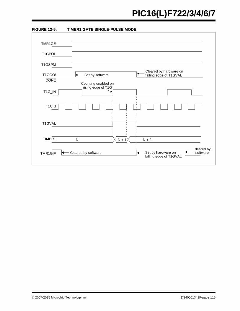
PIC16(L)F722/3/4/6/7
FIGURE 12-5: TIMER1 GATE SINGLE-PULSE MODE
TMR1GE
T1GPOL
T1G_IN
T1CKI
T1GVAL
TIMER1 N N + 1 N + 2
T1GSPM
T1GGO/
DONE
Set by softwareCleared by hardware onfalling edge of T1GVAL
Set by hardware onfalling edge of T1GVAL
Cleared by softwareCleared bysoftwareTMR1GIF
Counting enabled onrising edge of T1G
2007-2015 Microchip Technology Inc. DS40001341F-page 115

PIC16(L)F722/3/4/6/7
FIGURE 12-6: TIMER1 GATE SINGLE-PULSE AND TOGGLE COMBINED MODE
TMR1GE
T1GPOL
T1G_IN
T1CKI
T1GVAL
TIMER1 N N + 1 N + 2
T1GSPM
T1GGO/
DONE
Set by softwareCleared by hardware onfalling edge of T1GVAL
Set by hardware onfalling edge of T1GVALCleared by software
Cleared bysoftwareTMR1GIF
T1GTM
Counting enabled onrising edge of T1G
N + 4N + 3
DS40001341F-page 116 2007-2015 Microchip Technology Inc.

PIC16(L)F722/3/4/6/7
12.11 Timer1 Control Register
The Timer1 Control register (T1CON), shown inRegister 12-1, is used to control Timer1 and select thevarious features of the Timer1 module.
REGISTER 12-1: T1CON: TIMER1 CONTROL REGISTER
R/W-0 R/W-0 R/W-0 R/W-0 R/W-0 R/W-0 U-0 R/W-0
TMR1CS1 TMR1CS0 T1CKPS1 T1CKPS0 T1OSCEN T1SYNC — TMR1ON
bit 7 bit 0
Legend:
R = Readable bit W = Writable bit U = Unimplemented bit, read as ‘0’
-n = Value at POR ‘1’ = Bit is set ‘0’ = Bit is cleared x = Bit is unknown
bit 7-6 TMR1CS<1:0>: Timer1 Clock Source Select bits
11 = Timer1 clock source is Capacitive Sensing Oscillator (CAPOSC)10 = Timer1 clock source is pin or oscillator:
If T1OSCEN = 0:External clock from T1CKI pin (on the rising edge)If T1OSCEN = 1:Crystal oscillator on T1OSI/T1OSO pins
01 = Timer1 clock source is system clock (FOSC)00 = Timer1 clock source is instruction clock (FOSC/4)
bit 5-4 T1CKPS<1:0>: Timer1 Input Clock Prescale Select bits
11 = 1:8 Prescale value10 = 1:4 Prescale value01 = 1:2 Prescale value00 = 1:1 Prescale value
bit 3 T1OSCEN: LP Oscillator Enable Control bit
1 = Dedicated Timer1 oscillator circuit enabled0 = Dedicated Timer1 oscillator circuit disabled
bit 2 T1SYNC: Timer1 External Clock Input Synchronization Control bit
TMR1CS<1:0> = 1X1 = Do not synchronize external clock input0 = Synchronize external clock input with system clock (FOSC)
TMR1CS<1:0> = 0XThis bit is ignored. Timer1 uses the internal clock when TMR1CS<1:0> = 1X.
bit 1 Unimplemented: Read as ‘0’
bit 0 TMR1ON: Timer1 On bit
1 = Enables Timer10 = Stops Timer1Clears Timer1 Gate flip-flop
2007-2015 Microchip Technology Inc. DS40001341F-page 117

PIC16(L)F722/3/4/6/7
12.12 Timer1 Gate Control Register
The Timer1 Gate Control register (T1GCON), shown inRegister 12-2, is used to control Timer1 Gate.
REGISTER 12-2: T1GCON: TIMER1 GATE CONTROL REGISTER
R/W-0 R/W-0 R/W-0 R/W-0 R/W-0 R-x R/W-0 R/W-0
TMR1GE T1GPOL T1GTM T1GSPM T1GGO/DONE
T1GVAL T1GSS1 T1GSS0
bit 7 bit 0
Legend:
R = Readable bit W = Writable bit U = Unimplemented bit, read as ‘0’
-n = Value at POR ‘1’ = Bit is set ‘0’ = Bit is cleared x = Bit is unknown
bit 7 TMR1GE: Timer1 Gate Enable bit
If TMR1ON = 0:This bit is ignoredIf TMR1ON = 1:1 = Timer1 counting is controlled by the Timer1 gate function0 = Timer1 counts regardless of Timer1 gate function
bit 6 T1GPOL: Timer1 Gate Polarity bit
1 = Timer1 gate is active-high (Timer1 counts when gate is high)0 = Timer1 gate is active-low (Timer1 counts when gate is low)
bit 5 T1GTM: Timer1 Gate Toggle Mode bit
1 = Timer1 Gate Toggle mode is enabled.0 = Timer1 Gate Toggle mode is disabled and toggle flip flop is clearedTimer1 gate flip flop toggles on every rising edge.
bit 4 T1GSPM: Timer1 Gate Single Pulse Mode bit
1 = Timer1 gate Single-Pulse mode is enabled and is controlling Timer1 gate0 = Timer1 gate Single-Pulse mode is disabled
bit 3 T1GGO/DONE: Timer1 Gate Single-Pulse Acquisition Status bit
1 = Timer1 gate single-pulse acquisition is ready, waiting for an edge0 = Timer1 gate single-pulse acquisition has completed or has not been startedThis bit is automatically cleared when T1GSPM is cleared.
bit 2 T1GVAL: Timer1 Gate Current State bit
Indicates the current state of the Timer1 gate that could be provided to TMR1H:TMR1L.Unaffected by Timer1 Gate Enable (TMR1GE).
bit 1-0 T1GSS<1:0>: Timer1 Gate Source Select bits
00 = Timer1 Gate pin01 = Timer0 Overflow output10 = TMR2 Match PR2 output11 = Watchdog Timer scaler overflow
Watchdog Timer oscillator is turned on if TMR1GE = 1, regardless of the state of TMR1ON
DS40001341F-page 118 2007-2015 Microchip Technology Inc.

PIC16(L)F722/3/4/6/7
TABLE 12-6: SUMMARY OF REGISTERS ASSOCIATED WITH TIMER1
Name Bit 7 Bit 6 Bit 5 Bit 4 Bit 3 Bit 2 Bit 1 Bit 0Value on
POR, BOR
Value on all other Resets
ANSELB — — ANSB5 ANSB4 ANSB3 ANSB2 ANSB1 ANSB0 --11 1111 --11 1111
CCP1CON — — DC1B1 DC1B0 CCP1M3 CCP1M2 CCP1M1 CCP1M0 --00 0000 --00 0000
CCP2CON — — DC2B1 DC2B0 CCP2M3 CCP2M2 CCP2M1 CCP2M0 --00 0000 --00 0000
INTCON GIE PEIE T0IE INTE RBIE T0IF INTF RBIF 0000 000x 0000 000x
PIE1 TMR1GIE ADIE RCIE TXIE SSPIE CCP1IE TMR2IE TMR1IE 0000 0000 0000 0000
PIR1 TMR1GIF ADIF RCIF TXIF SSPIF CCP1IF TMR2IF TMR1IF 0000 0000 0000 0000
PORTB RB7 RB6 RB5 RB4 RB3 RB2 RB1 RB0 xxxx xxxx xxxx xxxx
TMR1H Holding Register for the Most Significant Byte of the 16-bit TMR1 Register xxxx xxxx uuuu uuuu
TMR1L Holding Register for the Least Significant Byte of the 16-bit TMR1 Register xxxx xxxx uuuu uuuu
TRISB TRISB7 TRISB6 TRISB5 TRISB4 TRISB3 TRISB2 TRISB1 TRISB0 1111 1111 1111 1111
TRISC TRISC7 TRISC6 TRISC5 TRISC4 TRISC3 TRISC2 TRISC1 TRISC0 1111 1111 1111 1111
T1CON TMR1CS1 TMR1CS0 T1CKPS1 T1CKPS0 T1OSCEN T1SYNC — TMR1ON 0000 00-0 uuuu uu-u
T1GCON TMR1GE T1GPOL T1GTM T1GSPM T1GGO/DONE
T1GVAL T1GSS1 T1GSS0 0000 0x00 uuuu uxuu
Legend: x = unknown, u = unchanged, — = unimplemented, read as ‘0’. Shaded cells are not used by the Timer1 module.
2007-2015 Microchip Technology Inc. DS40001341F-page 119

PIC16(L)F722/3/4/6/7
13.0 TIMER2 MODULE
The Timer2 module is an 8-bit timer with the followingfeatures:
• 8-bit timer register (TMR2)
• 8-bit period register (PR2)
• Interrupt on TMR2 match with PR2
• Software programmable prescaler (1:1, 1:4, 1:16)
• Software programmable postscaler (1:1 to 1:16)
See Figure 13-1 for a block diagram of Timer2.
13.1 Timer2 Operation
The clock input to the Timer2 module is the systeminstruction clock (FOSC/4). The clock is fed into theTimer2 prescaler, which has prescale options of 1:1,1:4 or 1:16. The output of the prescaler is then used toincrement the TMR2 register.
The values of TMR2 and PR2 are constantly comparedto determine when they match. TMR2 will incrementfrom 00h until it matches the value in PR2. When amatch occurs, two things happen:
• TMR2 is reset to 00h on the next increment cycle.
• The Timer2 postscaler is incremented.
The match output of the Timer2/PR2 comparator isthen fed into the Timer2 postscaler. The postscaler haspostscale options of 1:1 to 1:16 inclusive. The output ofthe Timer2 postscaler is used to set the TMR2IFinterrupt flag bit in the PIR1 register.
The TMR2 and PR2 registers are both fully readableand writable. On any Reset, the TMR2 register is set to00h and the PR2 register is set to FFh.
Timer2 is turned on by setting the TMR2ON bit in theT2CON register to a ‘1’. Timer2 is turned off by clearingthe TMR2ON bit to a ‘0’.
The Timer2 prescaler is controlled by the T2CKPS bitsin the T2CON register. The Timer2 postscaler iscontrolled by the TOUTPS bits in the T2CON register.The prescaler and postscaler counters are clearedwhen:
• A write to TMR2 occurs.
• A write to T2CON occurs.
• Any device Reset occurs (Power-on Reset, MCLR Reset, Watchdog Timer Reset, or Brown-out Reset).
FIGURE 13-1: TIMER2 BLOCK DIAGRAM
Note: TMR2 is not cleared when T2CON iswritten.
Comparator
TMR2Sets Flag
TMR2
Output
Reset
Postscaler
Prescaler
PR2
2
FOSC/4
1:1 to 1:16
1:1, 1:4, 1:16
EQ
4
bit TMR2IF
TOUTPS<3:0>
T2CKPS<1:0>
DS40001341F-page 120 2007-2015 Microchip Technology Inc.

PIC16(L)F722/3/4/6/7
TABLE 13-1: SUMMARY OF REGISTERS ASSOCIATED WITH TIMER2
REGISTER 13-1: T2CON: TIMER2 CONTROL REGISTER
U-0 R/W-0 R/W-0 R/W-0 R/W-0 R/W-0 R/W-0 R/W-0
— TOUTPS3 TOUTPS2 TOUTPS1 TOUTPS0 TMR2ON T2CKPS1 T2CKPS0
bit 7 bit 0
Legend:
R = Readable bit W = Writable bit U = Unimplemented bit, read as ‘0’
-n = Value at POR ‘1’ = Bit is set ‘0’ = Bit is cleared x = Bit is unknown
bit 7 Unimplemented: Read as ‘0’
bit 6-3 TOUTPS<3:0>: Timer2 Output Postscaler Select bits
0000 = 1:1 Postscaler0001 = 1:2 Postscaler0010 = 1:3 Postscaler0011 = 1:4 Postscaler0100 = 1:5 Postscaler0101 = 1:6 Postscaler0110 = 1:7 Postscaler0111 = 1:8 Postscaler1000 = 1:9 Postscaler1001 = 1:10 Postscaler1010 = 1:11 Postscaler1011 = 1:12 Postscaler1100 = 1:13 Postscaler1101 = 1:14 Postscaler1110 = 1:15 Postscaler1111 = 1:16 Postscaler
bit 2 TMR2ON: Timer2 On bit
1 = Timer2 is on0 = Timer2 is off
bit 1-0 T2CKPS<1:0>: Timer2 Clock Prescale Select bits
00 = Prescaler is 101 = Prescaler is 41x = Prescaler is 16
Name Bit 7 Bit 6 Bit 5 Bit 4 Bit 3 Bit 2 Bit 1 Bit 0Value on
POR, BOR
Value on all other Resets
INTCON GIE PEIE T0IE INTE RBIE T0IF INTF RBIF 0000 000x 0000 000x
PIE1 TMR1GIE ADIE RCIE TXIE SSPIE CCP1IE TMR2IE TMR1IE 0000 0000 0000 0000
PIR1 TMR1GIF ADIF RCIF TXIF SSPIF CCP1IF TMR2IF TMR1IF 0000 0000 0000 0000
PR2 Timer2 Module Period Register 1111 1111 1111 1111
TMR2 Holding Register for the 8-bit TMR2 Register 0000 0000 0000 0000
T2CON — TOUTPS3 TOUTPS2 TOUTPS1 TOUTPS0 TMR2ON T2CKPS1 T2CKPS0 -000 0000 -000 0000
Legend: x = unknown, u = unchanged, - = unimplemented read as ‘0’. Shaded cells are not used for Timer2 module.
2007-2015 Microchip Technology Inc. DS40001341F-page 121

PIC16(L)F722/3/4/6/7
14.0 CAPACITIVE SENSING MODULE
The capacitive sensing module allows for an interactionwith an end user without a mechanical interface. In atypical application, the capacitive sensing module isattached to a pad on a printed circuit board (PCB), whichis electrically isolated from the end user. When the enduser places their finger over the PCB pad, a capacitiveload is added, causing a frequency shift in the capacitive
sensing module. The capacitive sensing modulerequires software and at least one timer resource todetermine the change in frequency. Key features of thismodule include:
• Analog MUX for monitoring multiple inputs
• Capacitive sensing oscillator
• Multiple timer resources
• Software control
• Operation during Sleep
FIGURE 14-1: CAPACITIVE SENSING BLOCK DIAGRAM
T0CS
CPS0
CPS1
CPS2
CPS3
CPS4
CPS5
CPS6
CPS7
CPS8(1)
CPS9(1)
CPS10(1)
CPSCH<3:0>(2)
Capacitive Sensing
Oscillator
CPSOSC
CPSON
CPSRNG<1:0>
TMR00
1
SetT0IF
Overflow
T0XCS
0
1
T0CKI
T1CS<1:0>
T1OSC/T1CKI
TMR1H:TMR1LEN
T1GSEL<1:0>
Timer1 GateControl Logic
T1G
CPSOUT
TMR2
Timer2 Module
SetTMR2IF
Overflow Postscaler
CPS11(1)
CPS12(1)
CPS13(1)
CPS14(1)
CPS15(1)
CPSCLK
Note 1: Channels CPS<15:8> are implemented on PIC16F724/727/PIC16LF724/727 only.2: CPSCH3 is not implemented on PIC16F722/723/726/PIC16LF722/723/726.3: If CPSON = 0, disabling capacitive sensing, no channel is selected.
FOSC/4
FOSC
FOSC/4
Timer0 Module
Timer1 Module
CPSON(3)
WDT
WDTEvent
Overflow
Watchdog Timer Module
Scaler
PS<2:0>
LP WDTOSC
40001341F-page 122 2007-2015 Microchip Technology Inc.

PIC16(L)F722/3/4/6/7
14.1 Analog MUX
The capacitive sensing module can monitor up to 16inputs. The capacitive sensing inputs are defined asCPS<15:0>. To determine if a frequency change hasoccurred the user must:
• Select the appropriate CPS pin by setting the CPSCH<3:0> bits of the CPSCON1 register
• Set the corresponding ANSEL bit
• Set the corresponding TRIS bit
• Run the software algorithm
Selection of the CPSx pin while the module is enabledwill cause the capacitive sensing oscillator to be on theCPSx pin. Failure to set the corresponding ANSEL andTRIS bits can cause the capacitive sensing oscillator tostop, leading to false frequency readings.
14.2 Capacitive Sensing Oscillator
The capacitive sensing oscillator consists of a constantcurrent source and a constant current sink, to producea triangle waveform. The CPSOUT bit of theCPSCON0 register shows the status of the capacitivesensing oscillator, whether it is a sinking or sourcingcurrent. The oscillator is designed to drive a capacitiveload (single PCB pad) and at the same time, be a clocksource to either Timer0 or Timer1. The oscillator hasthree different current settings as defined byCPSRNG<1:0> of the CPSCON0 register. The differentcurrent settings for the oscillator serve two purposes:
• Maximize the number of counts in a timer for a fixed time base
• Maximize the count differential in the timer during a change in frequency
14.3 Timer resources
To measure the change in frequency of the capacitivesensing oscillator, a fixed time base is required. For theperiod of the fixed time base, the capacitive sensingoscillator is used to clock either Timer0 or Timer1. Thefrequency of the capacitive sensing oscillator is equalto the number of counts in the timer divided by theperiod of the fixed time base.
14.4 Fixed Time Base
To measure the frequency of the capacitive sensingoscillator, a fixed time base is required. Any timerresource or software loop can be used to establish thefixed time base. It is up to the end user to determine themethod in which the fixed time base is generated.
14.4.1 TIMER0
To select Timer0 as the timer resource for the capacitivesensing module:
• Set the T0XCS bit of the CPSCON0 register
• Clear the T0CS bit of the OPTION register
When Timer0 is chosen as the timer resource, thecapacitive sensing oscillator will be the clock source forTimer0. Refer to Section 11.0 “Timer0 Module” foradditional information.
14.4.2 TIMER1
To select Timer1 as the timer resource for thecapacitive sensing module, set the TMR1CS<1:0> ofthe T1CON register to ‘11’. When Timer1 is chosen asthe timer resource, the capacitive sensing oscillator willbe the clock source for Timer1. Because the Timer1module has a gate control, developing a time base forthe frequency measurement can be simplified usingeither:
• The Timer0 overflow flag
• The Timer2 overflow flag
• The WDT overflow flag
It is recommend that one of these flags, in conjunctionwith the toggle mode of the Timer1 Gate, is used todevelop the fixed time base required by the softwareportion of the capacitive sensing module. Refer toSection 12.0 “Timer1 Module with Gate Control” foradditional information.
TABLE 14-1: TIMER1 ENABLE FUNCTION
Note: The fixed time base can not be generatedby timer resource the capacitive sensingoscillator is clocking.
TMR1ON TMR1GE Timer1 Operation
0 0 Off
0 1 Off
1 0 On
1 1 Count Enabled by input
2007-2015 Microchip Technology Inc. 40001341F-page 123

PIC16(L)F722/3/4/6/7
14.5 Software Control
The software portion of the capacitive sensing moduleis required to determine the change in frequency of thecapacitive sensing oscillator. This is accomplished bythe following:
• Setting a fixed time base to acquire counts on Timer0 or Timer1
• Establishing the nominal frequency for the capacitive sensing oscillator
• Establishing the reduced frequency for the capacitive sensing oscillator due to an additional capacitive load
• Set the frequency threshold
14.5.1 NOMINAL FREQUENCY(NO CAPACITIVE LOAD)
To determine the nominal frequency of the capacitivesensing oscillator:
• Remove any extra capacitive load on the selected CPSx pin
• At the start of the fixed time base, clear the timer resource
• At the end of the fixed time base save the value in the timer resource
The value of the timer resource is the number ofoscillations of the capacitive sensing oscillator for thegiven time base. The frequency of the capacitivesensing oscillator is equal to the number of counts onin the timer divided by the period of the fixed time base.
14.5.2 REDUCED FREQUENCY (ADDITIONAL CAPACITIVE LOAD)
The extra capacitive load will cause the frequency of thecapacitive sensing oscillator to decrease. To determinethe reduced frequency of the capacitive sensingoscillator:
• Add a typical capacitive load on the selected CPSx pin
• Use the same fixed-time base as the nominal frequency measurement
• At the start of the fixed-time base, clear the timer resource
• At the end of the fixed-time base save the value in the timer resource
The value of the timer resource is the number ofoscillations of the capacitive sensing oscillator with anadditional capacitive load. The frequency of thecapacitive sensing oscillator is equal to the number ofcounts on in the timer divided by the period of the fixedtime base. This frequency should be less than thevalue obtained during the nominal frequencymeasurement.
14.5.3 FREQUENCY THRESHOLD
The frequency threshold should be placed midwaybetween the value of nominal frequency and thereduced frequency of the capacitive sensing oscillator.Refer to Application Note AN1103, Software Handlingfor Capacitive Sensing (DS01103) for more detailedinformation the software required for capacitivesensing module.
Note: For more information on generalCapacitive Sensing refer to ApplicationNotes:
• AN1101, Introduction to Capacitive Sensing (DS01101)
• AN1102, Layout and Physical Design Guidelines for Capacitive Sensing (DS01102).
40001341F-page 124 2007-2015 Microchip Technology Inc.

PIC16(L)F722/3/4/6/7
14.6 Operation during Sleep
The capacitive sensing oscillator will continue to run aslong as the module is enabled, independent of the partbeing in Sleep. In order for the software to determine ifa frequency change has occurred, the part must beawake. However, the part does not have to be awakewhen the timer resource is acquiring counts. One wayto acquire the Timer1 counts while in Sleep is to haveTimer1 gated with the overflow of the Watchdog Timer.This can be accomplished using the following steps:
1. Configure the Watchdog Time-out overflow asthe Timer1’s gate source T1GSS<1:0> = 11.
2. Set Timer1 Gate to toggle mode by setting theT1GTM bit of the T1GCON register.
3. Set the TMR1GE bit of the T1GCON register.
4. Set TMR1ON bit of the T1CON register.
5. Enable capacitive sensing module with theappropriate current settings and pin selection.
6. Clear Timer1.
7. Put the part to Sleep.
8. On the first WDT overflow, the capacitive sens-ing oscillator will begin to increment Timer1.Then put the part to Sleep.
9. On the second WDT overflow Timer1 will stopincrementing. Then run the software routine todetermine if a frequency change has occurred.
Refer to Section 12.0 “Timer1 Module with GateControl” for additional information.
Note 1: When using the WDT to set the intervalon Timer1, any other source that wakesthe part up early will cause the WDToverflow to be delayed, affecting thevalue captured by Timer1.
2: Timer0 does not operate when in Sleep,and therefore cannot be used forcapacitive sense measurements inSleep.
2007-2015 Microchip Technology Inc. 40001341F-page 125

PIC16(L)F722/3/4/6/7
REGISTER 14-1: CPSCON0: CAPACITIVE SENSING CONTROL REGISTER 0
R/W-0 U-0 U-0 U-0 R/W-0 R/W-0 R-0 R/W-0
CPSON — — — CPSRNG1 CPSRNG0 CPSOUT T0XCS
bit 7 bit 0
Legend:
R = Readable bit W = Writable bit U = Unimplemented bit, read as ‘0’
-n = Value at POR ‘1’ = Bit is set ‘0’ = Bit is cleared x = Bit is unknown
bit 7 CPSON: Capacitive Sensing Module Enable bit1 = Capacitive sensing module is operating0 = Capacitive sensing module is shut off and consumes no operating current
bit 6-4 Unimplemented: Read as ‘0’
bit 3-2 CPSRNG<1:0>: Capacitive Sensing Oscillator Range bits00 = Oscillator is Off.01 = Oscillator is in low range. Charge/discharge current is nominally 0.1 µA.10 = Oscillator is in medium range. Charge/discharge current is nominally 1.2 µA.11 = Oscillator is in high range. Charge/discharge current is nominally 18 µA.
bit 1 CPSOUT: Capacitive Sensing Oscillator Status bit1 = Oscillator is sourcing current (Current flowing out the pin)0 = Oscillator is sinking current (Current flowing into the pin)
bit 0 T0XCS: Timer0 External Clock Source Select bitIf T0CS = 1 The T0XCS bit controls which clock external to the core/Timer0 module supplies Timer0:1 = Timer0 Clock Source is the capacitive sensing oscillator0 = Timer0 Clock Source is the T0CKI pinIf T0CS = 0Timer0 clock source is controlled by the core/Timer0 module and is FOSC/4.
40001341F-page 126 2007-2015 Microchip Technology Inc.

PIC16(L)F722/3/4/6/7
TABLE 14-2: SUMMARY OF REGISTERS ASSOCIATED WITH CAPACITIVE SENSING
REGISTER 14-2: CPSCON1: CAPACITIVE SENSING CONTROL REGISTER 1
U-0 U-0 U-0 U-0 R/W-0(2) R/W-0 R/W-0 R/W-0
— — — — CPSCH3 CPSCH2 CPSCH1 CPSCH0
bit 7 bit 0
Legend:
R = Readable bit W = Writable bit U = Unimplemented bit, read as ‘0’
-n = Value at POR ‘1’ = Bit is set ‘0’ = Bit is cleared x = Bit is unknown
bit 7-4 Unimplemented: Read as ‘0’
bit 3-0 CPSCH<3:0>: Capacitive Sensing Channel Select bitsIf CPSON = 0:
These bits are ignored. No channel is selected.If CPSON = 1:
0000 = channel 0, (CPS0)0001 = channel 1, (CPS1)0010 = channel 2, (CPS2)0011 = channel 3, (CPS3)0100 = channel 4, (CPS4)0101 = channel 5, (CPS5)0110 = channel 6, (CPS6)0111 = channel 7, (CPS7)1000 = channel 8, (CPS8(1))1001 = channel 9, (CPS9(1))1010 = channel 10, (CPS10(1))1011 = channel 11, (CPS11(1))1100 = channel 12, (CPS12(1))1101 = channel 13, (CPS13(1))1110 = channel 14, (CPS14(1))1111 = channel 15, (CPS15(1))
Note 1: These channels are not implemented on the PIC16F722/723/726/PIC16LF722/723/726.
2: This bit is not implemented on PIC16F722/723/726/PIC16LF722/723/726, Read as ‘0’
Name Bit 7 Bit 6 Bit 5 Bit 4 Bit 3 Bit 2 Bit 1 Bit 0Value on
POR, BOR
Value onall otherResets
ANSELA — — ANSA5 ANSA4 ANSA3 ANSA2 ANSA1 ANSA0 --11 1111 --11 1111
ANSELB — — ANSB5 ANSB4 ANSB3 ANSB2 ANSB1 ANSB0 --11 1111 --11 1111
ANSELD ANSD7 ANSD6 ANSD5 ANSD4 ANSD3 ANSD2 ANSD1 ANSD0 1111 1111 1111 1111
OPTION_REG RBPU INTEDG T0CS T0SE PSA PS2 PS1 PS0 1111 1111 1111 1111
PIE1 TMR1GIE ADIE RCIE TXIE SSPIE CCP1IE TMR2IE TMR1IE 0000 0000 0000 0000
PIR1 TMR1GIF ADIF RCIF TXIF SSPIF CCP1IF TMR2IF TMR1IF 0000 0000 0000 0000
T1CON TMR1CS1 TMR1CS0 T1CKPS1 T1CKPS0 T1OSCEN T1SYNC — TMR1ON 0000 00-0 0000 00-0
T2CON — TOUTPS3 TOUTPS2 TOUTPS1 TOUTPS0 TMR2ON T2CKPS1 T2CKPS0 -000 0000 -000 0000
TRISA TRISA7 TRISA6 TRISA5 TRISA4 TRISA3 TRISA2 TRISA1 TRISA0 1111 1111 1111 1111
TRISB TRISB7 TRISB6 TRISB5 TRISB4 TRISB3 TRISB2 TRISB1 TRISB0 1111 1111 1111 1111
TRISD TRISD7 TRISD6 TRISD5 TRISD4 TRISD3 TRISD2 TRISD1 TRISD0 1111 1111 1111 1111
Legend: - = Unimplemented locations, read as ‘0’, u = unchanged, x = unknown. Shaded cells are not used by the capacitive sensing module.
2007-2015 Microchip Technology Inc. 40001341F-page 127

PIC16(L)F722/3/4/6/7
15.0 CAPTURE/COMPARE/PWM (CCP) MODULE
The Capture/Compare/PWM module is a peripheralwhich allows the user to time and control differentevents. In Capture mode, the peripheral allows thetiming of the duration of an event. The Compare modeallows the user to trigger an external event when apredetermined amount of time has expired. The PWMmode can generate a pulse-width modulated signal ofvarying frequency and duty cycle.
The timer resources used by the module are shown inTable 15-1.
Additional information on CCP modules is available inthe Application Note AN594, Using the CCP Modules(DS00594).
TABLE 15-1: CCP MODE – TIMER RESOURCES REQUIRED
TABLE 15-2: INTERACTION OF TWO CCP MODULES
CCP Mode Timer Resource
Capture Timer1
Compare Timer1
PWM Timer2
CCP1 Mode CCP2 Mode Interaction
Capture Capture Same TMR1 time base
Capture Compare Same TMR1 time base(1, 2)
Compare Compare Same TMR1 time base(1, 2)
PWM PWM The PWMs will have the same frequency and update rate (TMR2 interrupt).The rising edges will be aligned.
PWM Capture None
PWM Compare None
Note 1: If CCP2 is configured as a Special Event Trigger, CCP1 will clear Timer1, affecting the value captured on the CCP2 pin.
2: If CCP1 is in Capture mode and CCP2 is configured as a Special Event Trigger, CCP2 will clear Timer1, affecting the value captured on the CCP1 pin.
Note: CCPRx and CCPx throughout thisdocument refer to CCPR1 or CCPR2 andCCP1 or CCP2, respectively
DS40001341F-page 128 2007-2015 Microchip Technology Inc.

PIC16(L)F722/3/4/6/7
REGISTER 15-1: CCPxCON: CCPx CONTROL REGISTER
U-0 U-0 R/W-0 R/W-0 R/W-0 R/W-0 R/W-0 R/W-0
— — DCxB1 DCxB0 CCPxM3 CCPxM2 CCPxM1 CCPxM0
bit 7 bit 0
Legend:
R = Readable bit W = Writable bit U = Unimplemented bit, read as ‘0’
-n = Value at POR ‘1’ = Bit is set ‘0’ = Bit is cleared x = Bit is unknown
bit 7-6 Unimplemented: Read as ‘0’
bit 5-4 DCxB<1:0>: PWM Duty Cycle Least Significant bitsCapture mode: UnusedCompare mode: UnusedPWM mode: These bits are the two LSbs of the PWM duty cycle. The eight MSbs are found in CCPRxL.
bit 3-0 CCPxM<3:0>: CCP Mode Select bits0000 = Capture/Compare/PWM off (resets CCP module)0001 = Unused (reserved)0010 = Compare mode, toggle output on match (CCPxIF bit of the PIRx register is set)0011 = Unused (reserved)0100 = Capture mode, every falling edge0101 = Capture mode, every rising edge0110 = Capture mode, every 4th rising edge0111 = Capture mode, every 16th rising edge1000 = Compare mode, set output on match (CCPxIF bit of the PIRx register is set)1001 = Compare mode, clear output on match (CCPxIF bit of the PIRx register is set)1010 = Compare mode, generate software interrupt on match (CCPxIF bit is set of the PIRx register,
CCPx pin is unaffected)1011 = Compare mode, trigger special event (CCPxIF bit of the PIRx register is set, TMR1 is reset
and A/D conversion(1) is started if the ADC module is enabled. CCPx pin is unaffected.)11xx = PWM mode.
Note 1: A/D conversion start feature is available only on CCP2.
2007-2015 Microchip Technology Inc. DS40001341F-page 129

PIC16(L)F722/3/4/6/7
15.1 Capture Mode
In Capture mode, CCPRxH:CCPRxL captures the16-bit value of the TMR1 register when an event occurson pin CCPx. An event is defined as one of thefollowing and is configured by the CCPxM<3:0> bits ofthe CCPxCON register:
• Every falling edge
• Every rising edge
• Every 4th rising edge
• Every 16th rising edge
When a capture is made, the Interrupt Request Flag bitCCPxIF of the PIRx register is set. The interrupt flagmust be cleared in software. If another capture occursbefore the value in the CCPRxH, CCPRxL register pairis read, the old captured value is overwritten by the newcaptured value (refer to Figure 15-1).
15.1.1 CCPx PIN CONFIGURATION
In Capture mode, the CCPx pin should be configuredas an input by setting the associated TRIS control bit.
Either RC1 or RB3 can be selected as the CCP2 pin.Refer to Section 6.1 “Alternate Pin Function” formore information.
FIGURE 15-1: CAPTURE MODE OPERATION BLOCK DIAGRAM
15.1.2 TIMER1 MODE SELECTION
Timer1 must be running in Timer mode or SynchronizedCounter mode for the CCP module to use the capturefeature. In Asynchronous Counter mode or whenTimer1 is clocked at FOSC, the capture operation maynot work.
15.1.3 SOFTWARE INTERRUPT
When the Capture mode is changed, a false captureinterrupt may be generated. The user should keep theCCPxIE interrupt enable bit of the PIEx register clear toavoid false interrupts. Additionally, the user shouldclear the CCPxIF interrupt flag bit of the PIRx registerfollowing any change in operating mode.
15.1.4 CCP PRESCALER
There are four prescaler settings specified by theCCPxM<3:0> bits of the CCPxCON register. Wheneverthe CCP module is turned off, or the CCP module is notin Capture mode, the prescaler counter is cleared. AnyReset will clear the prescaler counter.
Switching from one capture prescaler to another does notclear the prescaler and may generate a false interrupt. Toavoid this unexpected operation, turn the module off byclearing the CCPxCON register before changing theprescaler (refer to Example 15-1).
EXAMPLE 15-1: CHANGING BETWEEN CAPTURE PRESCALERS
15.1.5 CAPTURE DURING SLEEP
Capture mode depends upon the Timer1 module forproper operation. There are two options for driving theTimer1 module in Capture mode. It can be driven by theinstruction clock (FOSC/4), or by an external clocksource.
If Timer1 is clocked by FOSC/4, then Timer1 will notincrement during Sleep. When the device wakes fromSleep, Timer1 will continue from its previous state.
If Timer1 is clocked by an external clock source, thenCapture mode will operate as defined in Section 15.1“Capture Mode”.
Note: If the CCPx pin is configured as an output,a write to the port can cause a capturecondition.
CCPRxH CCPRxL
TMR1H TMR1L
Set Flag bit CCPxIF(PIRx register)
CaptureEnable
CCPxCON<3:0>
Prescaler 1, 4, 16
andEdge Detect
CCPx
System Clock (FOSC)
Note: Clocking Timer1 from the system clock(FOSC) should not be used in CaptureMode. In order for Capture Mode to recog-nize the trigger event on the CCPx pin,Timer1 must be clocked from the Instruc-tion Clock (FOSC/4) or from an externalclock source.
BANKSEL CCP1CON ;Set Bank bits to point;to CCP1CON
CLRF CCP1CON ;Turn CCP module offMOVLW NEW_CAPT_PS;Load the W reg with
; the new prescaler; move value and CCP ON
MOVWF CCP1CON ;Load CCP1CON with this; value
DS40001341F-page 130 2007-2015 Microchip Technology Inc.

PIC16(L)F722/3/4/6/7
TABLE 15-3: SUMMARY OF REGISTERS ASSOCIATED WITH CAPTURE
Name Bit 7 Bit 6 Bit 5 Bit 4 Bit 3 Bit 2 Bit 1 Bit 0Value on
POR, BOR
Value onall otherResets
ANSELB — — ANSB5 ANSB4 ANSB3 ANSB2 ANSB1 ANSB0 --11 1111 --11 1111
APFCON — — — — — — SSSEL CCP2SEL ---- --00 ---- --00
CCP1CON — — DC1B1 DC1B0 CCP1M3 CCP1M2 CCP1M1 CCP1M0 --00 0000 --00 0000
CCP2CON — — DC2B1 DC2B0 CCP2M3 CCP2M2 CCP2M1 CCP2M0 --00 0000 --00 0000
CCPRxL Capture/Compare/PWM Register X Low Byte xxxx xxxx uuuu uuuu
CCPRxH Capture/Compare/PWM Register X High Byte xxxx xxxx uuuu uuuu
INTCON GIE PEIE T0IE INTE RBIE T0IF INTF RBIF 0000 000x 0000 000x
PIE1 TMR1GIE ADIE RCIE TXIE SSPIE CCP1IE TMR2IE TMR1IE 0000 0000 0000 0000
PIE2 — — — — — — — CCP2IE ---- ---0 ---- ---0
PIR1 TMR1GIF ADIF RCIF TXIF SSPIF CCP1IF TMR2IF TMR1IF 0000 0000 0000 0000
PIR2 — — — — — — — CCP2IF ---- ---0 ---- ---0
T1CON TMR1CS1 TMR1CS0 T1CKPS1 T1CKPS0 T1OSCEN T1SYNC — TMR1ON 0000 00-0 uuuu uu-u
T1GCON TMR1GE T1GPOL T1GTM T1GSPM T1GGO/DONE
T1GVAL T1GSS1 T1GSS0 0000 0x00 0000 0x00
TMR1L Holding Register for the Least Significant Byte of the 16-bit TMR1 Register xxxx xxxx uuuu uuuu
TMR1H Holding Register for the Most Significant Byte of the 16-bit TMR1 Register xxxx xxxx uuuu uuuu
TRISB TRISB7 TRISB6 TRISB5 TRISB4 TRISB3 TRISB2 TRISB1 TRISB0 1111 1111 1111 1111
TRISC TRISC7 TRISC6 TRISC5 TRISC4 TRISC3 TRISC2 TRISC1 TRISC0 1111 1111 1111 1111
Legend: - = Unimplemented locations, read as ‘0’, u = unchanged, x = unknown. Shaded cells are not used by the Capture.
2007-2015 Microchip Technology Inc. DS40001341F-page 131

PIC16(L)F722/3/4/6/7
15.2 Compare Mode
In Compare mode, the 16-bit CCPRx register value isconstantly compared against the TMR1 register pairvalue. When a match occurs, the CCPx module may:
• Toggle the CCPx output
• Set the CCPx output
• Clear the CCPx output
• Generate a Special Event Trigger
• Generate a Software Interrupt
The action on the pin is based on the value of theCCPxM<3:0> control bits of the CCPxCON register.
All Compare modes can generate an interrupt.
FIGURE 15-2: COMPARE MODE OPERATION BLOCK DIAGRAM
15.2.1 CCPx PIN CONFIGURATION
The user must configure the CCPx pin as an output byclearing the associated TRIS bit.
Either RC1 or RB3 can be selected as the CCP2 pin.Refer to Section 6.1 “Alternate Pin Function” formore information.
15.2.2 TIMER1 MODE SELECTION
In Compare mode, Timer1 must be running in eitherTimer mode or Synchronized Counter mode. Thecompare operation may not work in AsynchronousCounter mode.
15.2.3 SOFTWARE INTERRUPT MODE
When Software Interrupt mode is chosen(CCPxM<3:0> = 1010), the CCPxIF bit in the PIRxregister is set and the CCPx module does not assertcontrol of the CCPx pin (refer to the CCPxCONregister).
15.2.4 SPECIAL EVENT TRIGGER
When Special Event Trigger mode is chosen(CCPxM<3:0> = 1011), the CCPx module does thefollowing:
• Resets Timer1
• Starts an ADC conversion if ADC is enabled (CCP2 only)
The CCPx module does not assert control of the CCPxpin in this mode (refer to the CCPxCON register).
The Special Event Trigger output of the CCP occursimmediately upon a match between the TMR1H,TMR1L register pair and the CCPRxH, CCPRxLregister pair. The TMR1H, TMR1L register pair is notreset until the next rising edge of the Timer1 clock. Thisallows the CCPRxH, CCPRxL register pair toeffectively provide a 16-bit programmable periodregister for Timer1.
15.2.5 COMPARE DURING SLEEP
The Compare Mode is dependent upon the systemclock (FOSC) for proper operation. Since FOSC is shutdown during Sleep mode, the Compare mode will notfunction properly during Sleep.
Note: Clearing the CCPxCON register will forcethe CCPx compare output latch to thedefault low level. This is not the PORT I/Odata latch.
CCPRxH CCPRxL
TMR1H TMR1L
ComparatorQ S
R
OutputLogic
Special Event Trigger
Set CCPxIF Interrupt Flag(PIRx)
Match
TRIS
CCPxCON<3:0>Mode Select
Output Enable
Special Event Trigger will:
• Clear TMR1H and TMR1L registers.• NOT set interrupt flag bit TMR1IF of the PIR1 register.• Set the GO/DONE bit to start the ADC conversion
(CCP2 only).
CCPx4
Note: Clocking Timer1 from the system clock(FOSC) should not be used in Comparemode. For the Compare operation of theTMR1 register to the CCPRx register tooccur, Timer1 must be clocked from theInstruction Clock (FOSC/4) or from anexternal clock source.
Note 1: The Special Event Trigger from the CCPmodule does not set interrupt flag bitTMR1IF of the PIR1 register.
2: Removing the match condition bychanging the contents of the CCPRxHand CCPRxL register pair, between theclock edge that generates the SpecialEvent Trigger and the clock edge thatgenerates the Timer1 Reset, willpreclude the Reset from occurring.
DS40001341F-page 132 2007-2015 Microchip Technology Inc.

PIC16(L)F722/3/4/6/7
TABLE 15-4: SUMMARY OF REGISTERS ASSOCIATED WITH COMPARE
Name Bit 7 Bit 6 Bit 5 Bit 4 Bit 3 Bit 2 Bit 1 Bit 0Value on
POR, BOR
Value onall otherResets
ADCON0 — — CHS3 CHS2 CHS1 CHS0 GO/DONE ADON --00 0000 --00 0000
ANSELB — — ANSB5 ANSB4 ANSB3 ANSB2 ANSB1 ANSB0 --11 1111 --11 1111
APFCON — — — — — — SSSEL CCP2SEL ---- --00 ---- --00
CCP1CON — — DC1B1 DC1B0 CCP1M3 CCP1M2 CCP1M1 CCP1M0 --00 0000 --00 0000
CCP2CON — — DC2B1 DC2B0 CCP2M3 CCP2M2 CCP2M1 CCP2M0 --00 0000 --00 0000
CCPRxL Capture/Compare/PWM Register X Low Byte xxxx xxxx uuuu uuuu
CCPRxH Capture/Compare/PWM Register X High Byte xxxx xxxx uuuu uuuu
INTCON GIE PEIE T0IE INTE RBIE T0IF INTF RBIF 0000 000x 0000 000x
PIE1 TMR1GIE ADIE RCIE TXIE SSPIE CCP1IE TMR2IE TMR1IE 0000 0000 0000 0000
PIE2 — — — — — — — CCP2IE ---- ---0 ---- ---0
PIR1 TMR1GIF ADIF RCIF TXIF SSPIF CCP1IF TMR2IF TMR1IF 0000 0000 0000 0000
PIR2 — — — — — — — CCP2IF ---- ---0 ---- ---0
T1CON TMR1CS1 TMR1CS0 T1CKPS1 T1CKPS0 T1OSCEN T1SYNC — TMR1ON 0000 00-0 uuuu uu-u
T1GCON TMR1GE T1GPOL T1GTM T1GSPM T1GGO/DONE
T1GVAL T1GSS1 T1GSS0 0000 0x00 0000 0x00
TMR1L Holding Register for the Least Significant Byte of the 16-bit TMR1 Register xxxx xxxx uuuu uuuu
TMR1H Holding Register for the Most Significant Byte of the 16-bit TMR1 Register xxxx xxxx uuuu uuuu
TRISB TRISB7 TRISB6 TRISB5 TRISB4 TRISB3 TRISB2 TRISB1 TRISB0 1111 1111 1111 1111
TRISC TRISC7 TRISC6 TRISC5 TRISC4 TRISC3 TRISC2 TRISC1 TRISC0 1111 1111 1111 1111
Legend: - = Unimplemented locations, read as ‘0’, u = unchanged, x = unknown. Shaded cells are not used by the Compare.
2007-2015 Microchip Technology Inc. DS40001341F-page 133

PIC16(L)F722/3/4/6/7
15.3 PWM Mode
The PWM mode generates a Pulse-Width Modulatedsignal on the CCPx pin. The duty cycle, period andresolution are determined by the following registers:
• PR2
• T2CON
• CCPRxL
• CCPxCON
In Pulse-Width Modulation (PWM) mode, the CCPmodule produces up to a 10-bit resolution PWM outputon the CCPx pin.
Figure 15-3 shows a simplified block diagram of PWMoperation.
Figure 15-4 shows a typical waveform of the PWMsignal.
For a step-by-step procedure on how to set up the CCPmodule for PWM operation, refer to Section 15.3.8“Setup for PWM Operation”.
FIGURE 15-3: SIMPLIFIED PWM BLOCK DIAGRAM
The PWM output (Figure 15-4) has a time base(period) and a time that the output stays high (dutycycle).
FIGURE 15-4: CCP PWM OUTPUT
15.3.1 CCPx PIN CONFIGURATION
In PWM mode, the CCPx pin is multiplexed with thePORT data latch. The user must configure the CCPxpin as an output by clearing the associated TRIS bit.
Either RC1 or RB3 can be selected as the CCP2 pin.Refer to Section 6.1 “Alternate Pin Function” formore information.
CCPRxL
CCPRxH(2) (Slave)
Comparator
TMR2
PR2
(1)
R Q
S
Duty Cycle RegistersCCPxCON<5:4>
Clear Timer2,toggle CCPx pin and latch duty cycle
Note 1: The 8-bit timer TMR2 register is concatenated with the 2-bit internal system clock (FOSC), or 2 bits of the prescaler, to create the 10-bit time base.
2: In PWM mode, CCPRxH is a read-only register.
TRIS
CCPx
Comparator
Note: Clearing the CCPxCON register willrelinquish CCPx control of the CCPx pin.
Period
Pulse Width
TMR2 = 0
TMR2 = CCPRxL:CCPxCON<5:4>
TMR2 = PR2
DS40001341F-page 134 2007-2015 Microchip Technology Inc.
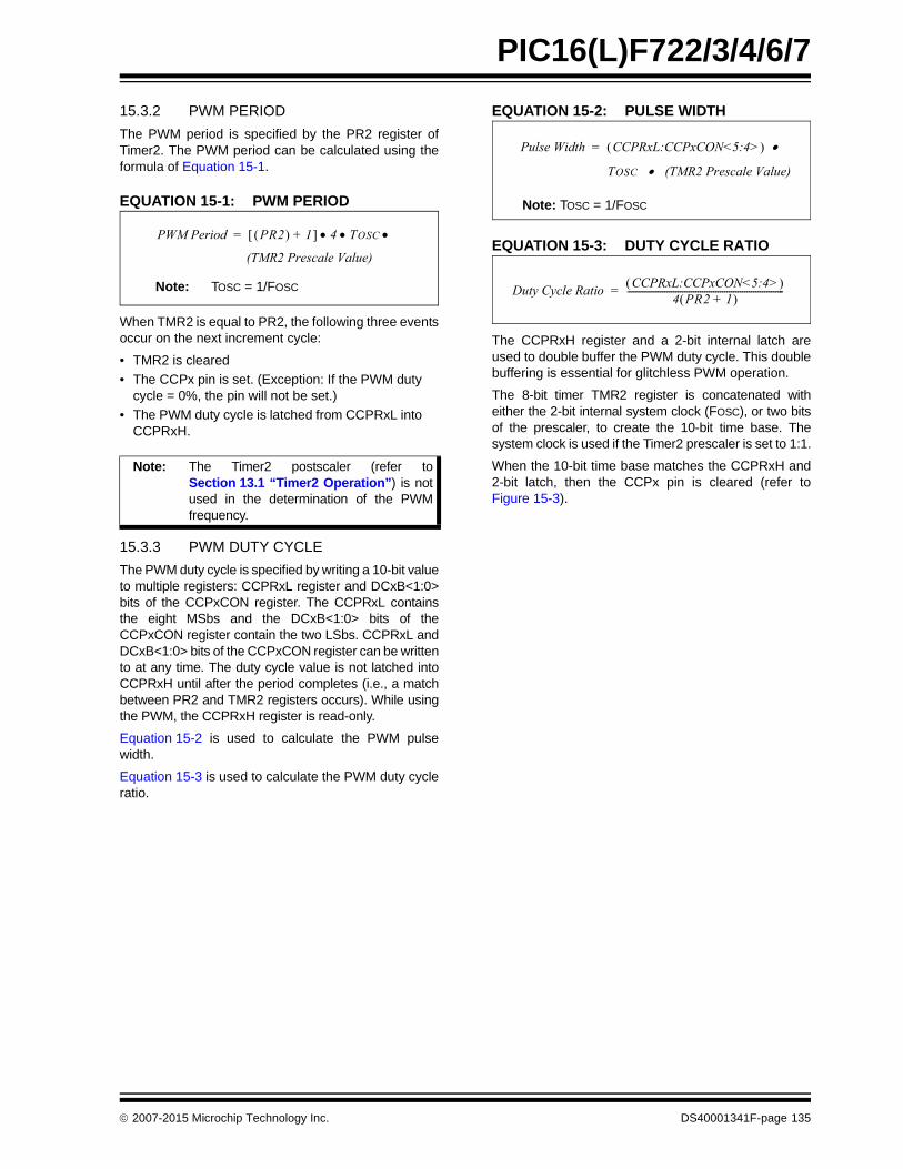
PIC16(L)F722/3/4/6/7
15.3.2 PWM PERIOD
The PWM period is specified by the PR2 register ofTimer2. The PWM period can be calculated using theformula of Equation 15-1.
EQUATION 15-1: PWM PERIOD
When TMR2 is equal to PR2, the following three eventsoccur on the next increment cycle:
• TMR2 is cleared
• The CCPx pin is set. (Exception: If the PWM duty cycle = 0%, the pin will not be set.)
• The PWM duty cycle is latched from CCPRxL into CCPRxH.
15.3.3 PWM DUTY CYCLE
The PWM duty cycle is specified by writing a 10-bit valueto multiple registers: CCPRxL register and DCxB<1:0>bits of the CCPxCON register. The CCPRxL containsthe eight MSbs and the DCxB<1:0> bits of theCCPxCON register contain the two LSbs. CCPRxL andDCxB<1:0> bits of the CCPxCON register can be writtento at any time. The duty cycle value is not latched intoCCPRxH until after the period completes (i.e., a matchbetween PR2 and TMR2 registers occurs). While usingthe PWM, the CCPRxH register is read-only.
Equation 15-2 is used to calculate the PWM pulsewidth.
Equation 15-3 is used to calculate the PWM duty cycleratio.
EQUATION 15-2: PULSE WIDTH
EQUATION 15-3: DUTY CYCLE RATIO
The CCPRxH register and a 2-bit internal latch areused to double buffer the PWM duty cycle. This doublebuffering is essential for glitchless PWM operation.
The 8-bit timer TMR2 register is concatenated witheither the 2-bit internal system clock (FOSC), or two bitsof the prescaler, to create the 10-bit time base. Thesystem clock is used if the Timer2 prescaler is set to 1:1.
When the 10-bit time base matches the CCPRxH and2-bit latch, then the CCPx pin is cleared (refer toFigure 15-3).
Note: The Timer2 postscaler (refer toSection 13.1 “Timer2 Operation”) is notused in the determination of the PWMfrequency.
PWM Period PR2 1+ 4 TOSC =
(TMR2 Prescale Value)
Note: TOSC = 1/FOSC
Pulse Width CCPRxL:CCPxCON<5:4> =
TOSC (TMR2 Prescale Value)
Note: TOSC = 1/FOSC
Duty Cycle RatioCCPRxL:CCPxCON<5:4>
4 PR2 1+ -----------------------------------------------------------------------=
2007-2015 Microchip Technology Inc. DS40001341F-page 135

PIC16(L)F722/3/4/6/7
15.3.4 PWM RESOLUTION
The resolution determines the number of available dutycycles for a given period. For example, a 10-bit resolutionwill result in 1024 discrete duty cycles, whereas an 8-bitresolution will result in 256 discrete duty cycles.
The maximum PWM resolution is ten bits when PR2 is255. The resolution is a function of the PR2 registervalue as shown by Equation 15-4.
EQUATION 15-4: PWM RESOLUTION
TABLE 15-5: EXAMPLE PWM FREQUENCIES AND RESOLUTIONS (FOSC = 20 MHz)
TABLE 15-6: EXAMPLE PWM FREQUENCIES AND RESOLUTIONS (FOSC = 8 MHz)
15.3.5 OPERATION IN SLEEP MODE
In Sleep mode, the TMR2 register will not incrementand the state of the module will not change. If the CCPxpin is driving a value, it will continue to drive that value.When the device wakes up, TMR2 will continue from itsprevious state.
15.3.6 CHANGES IN SYSTEM CLOCK FREQUENCY
The PWM frequency is derived from the system clockfrequency (FOSC). Any changes in the system clock fre-quency will result in changes to the PWM frequency.Refer to Section 7.0 “Oscillator Module” foradditional details.
15.3.7 EFFECTS OF RESET
Any Reset will force all ports to Input mode and theCCP registers to their Reset states.
15.3.8 SETUP FOR PWM OPERATION
The following steps should be taken when configuringthe CCP module for PWM operation:
1. Disable the PWM pin (CCPx) output driver(s) bysetting the associated TRIS bit(s).
2. Load the PR2 register with the PWM period value.
3. Configure the CCP module for the PWM modeby loading the CCPxCON register with theappropriate values.
4. Load the CCPRxL register and the DCxBx bits ofthe CCPxCON register, with the PWM duty cyclevalue.
5. Configure and start Timer2:
• Clear the TMR2IF interrupt flag bit of the PIR1 register. See Note below.
• Configure the T2CKPS bits of the T2CON register with the Timer2 prescale value.
• Enable Timer2 by setting the TMR2ON bit of the T2CON register.
6. Enable PWM output pin:
• Wait until Timer2 overflows, TMR2IF bit of the PIR1 register is set. See Note below.
• Enable the PWM pin (CCPx) output driver(s) by clearing the associated TRIS bit(s).
Note: If the pulse-width value is greater than theperiod, the assigned PWM pin(s) willremain unchanged.
Resolution4 PR2 1+ log
2 log------------------------------------------ bits=
PWM Frequency 1.22 kHz 4.88 kHz 19.53 kHz 78.12 kHz 156.3 kHz 208.3 kHz
Timer Prescale (1, 4, 16) 16 4 1 1 1 1
PR2 Value 0xFF 0xFF 0xFF 0x3F 0x1F 0x17
Maximum Resolution (bits) 10 10 10 8 7 6.6
PWM Frequency 1.22 kHz 4.90 kHz 19.61 kHz 76.92 kHz 153.85 kHz 200.0 kHz
Timer Prescale (1, 4, 16) 16 4 1 1 1 1
PR2 Value 0x65 0x65 0x65 0x19 0x0C 0x09
Maximum Resolution (bits) 8 8 8 6 5 5
Note: In order to send a complete duty cycle andperiod on the first PWM output, the abovesteps must be included in the setupsequence. If it is not critical to start with acomplete PWM signal on the first output,then step 6 may be ignored.
DS40001341F-page 136 2007-2015 Microchip Technology Inc.

PIC16(L)F722/3/4/6/7
TABLE 15-7: SUMMARY OF REGISTERS ASSOCIATED WITH PWM
Name Bit 7 Bit 6 Bit 5 Bit 4 Bit 3 Bit 2 Bit 1 Bit 0Value on
POR, BOR
Value onall otherResets
ANSELB — — ANSB5 ANSB4 ANSB3 ANSB2 ANSB1 ANSB0 --11 1111 --11 1111
APFCON — — — — — — SSSEL CCP2SEL ---- --00 ---- --00
CCP1CON — — DC1B1 DC1B0 CCP1M3 CCP1M2 CCP1M1 CCP1M0 --00 0000 --00 0000
CCP2CON — — DC2B1 DC2B0 CCP2M3 CCP2M2 CCP2M1 CCP2M0 --00 0000 --00 0000
CCPRxL Capture/Compare/PWM Register X Low Byte xxxx xxxx uuuu uuuu
CCPRxH Capture/Compare/PWM Register X High Byte xxxx xxxx uuuu uuuu
PR2 Timer2 Period Register 1111 1111 1111 1111
T2CON — TOUTPS3 TOUTPS2 TOUTPS1 TOUTPS0 TMR2ON T2CKPS1 T2CKPS0 -000 0000 -000 0000
TMR2 Timer2 Module Register 0000 0000 0000 0000
TRISB TRISB7 TRISB6 TRISB5 TRISB4 TRISB3 TRISB2 TRISB1 TRISB0 1111 1111 1111 1111
TRISC TRISC7 TRISC6 TRISC5 TRISC4 TRISC3 TRISC2 TRISC1 TRISC0 1111 1111 1111 1111
Legend: - = Unimplemented locations, read as ‘0’, u = unchanged, x = unknown. Shaded cells are not used by the PWM.
2007-2015 Microchip Technology Inc. DS40001341F-page 137

PIC16(L)F722/3/4/6/7
16.0 ADDRESSABLE UNIVERSAL SYNCHRONOUS ASYNCHRONOUS RECEIVER TRANSMITTER (AUSART)
The Addressable Universal SynchronousAsynchronous Receiver Transmitter (AUSART)module is a serial I/O communications peripheral. Itcontains all the clock generators, shift registers anddata buffers necessary to perform an input or outputserial data transfer independent of device programexecution. The AUSART, also known as a SerialCommunications Interface (SCI), can be configured asa full-duplex asynchronous system or half-duplexsynchronous system. Full-Duplex mode is useful forcommunications with peripheral systems, such as CRTterminals and personal computers. Half-DuplexSynchronous mode is intended for communicationswith peripheral devices, such as A/D or D/A integratedcircuits, serial EEPROMs or other microcontrollers.These devices typically do not have internal clocks forbaud rate generation and require the external clocksignal provided by a master synchronous device.
The AUSART module includes the following capabilities:
• Full-duplex asynchronous transmit and receive
• Two-character input buffer
• One-character output buffer
• Programmable 8-bit or 9-bit character length
• Address detection in 9-bit mode
• Input buffer overrun error detection
• Received character framing error detection
• Half-duplex synchronous master
• Half-duplex synchronous slave
• Sleep operation
Block diagrams of the AUSART transmitter andreceiver are shown in Figure 16-1 and Figure 16-2.
FIGURE 16-1: AUSART TRANSMIT BLOCK DIAGRAM
TXIF
TXIE
Interrupt
TXEN
TX9D
MSb LSb
Data Bus
TXREG Register
Transmit Shift Register (TSR)
(8) 0
TX9
TRMT SPEN
TX/CK
Pin Bufferand Control
8
SPBRG
FOSC÷ n
n
+ 1 Multiplier x4 x16 x64
SYNC 1 0 0
BRGH x 1 0
Baud Rate Generator
• • •
DS40001341F-page 138 2007-2015 Microchip Technology Inc.

PIC16(L)F722/3/4/6/7
FIGURE 16-2: AUSART RECEIVE BLOCK DIAGRAM
The operation of the AUSART module is controlledthrough two registers:
• Transmit Status and Control (TXSTA)
• Receive Status and Control (RCSTA)
These registers are detailed in Register 16-1 andRegister 16-2, respectively.
RX/DT
Pin Bufferand Control
SPEN
DataRecovery
CREN OERR
FERR
RSR RegisterMSb LSb
RX9D RCREG RegisterFIFO
InterruptRCIFRCIE
Data Bus8
Stop START(8) 7 1 0
RX9
• • •
SPBRG
FOSC÷ n
n+ 1 Multiplier x4 x16 x64
SYNC 1 0 0
BRGH x 1 0
Baud Rate Generator
2007-2015 Microchip Technology Inc. DS40001341F-page 139

PIC16(L)F722/3/4/6/7
16.1 AUSART Asynchronous Mode
The AUSART transmits and receives data using thestandard non-return-to-zero (NRZ) format. NRZ isimplemented with two levels: a VOH Mark state whichrepresents a ‘1’ data bit, and a VOL Space state whichrepresents a ‘0’ data bit. NRZ refers to the fact thatconsecutively transmitted data bits of the same valuestay at the output level of that bit without returning to aneutral level between each bit transmission. An NRZtransmission port idles in the Mark state. Each charactertransmission consists of one Start bit followed by eightor nine data bits and is always terminated by one ormore Stop bits. The Start bit is always a space and theStop bits are always marks. The most common dataformat is 8 bits. Each transmitted bit persists for a periodof 1/(Baud Rate). An on-chip dedicated 8-bit Baud RateGenerator is used to derive standard baud ratefrequencies from the system oscillator. Refer toTable 16-5 for examples of baud rate Configurations.
The AUSART transmits and receives the LSb first. TheAUSART’s transmitter and receiver are functionallyindependent, but share the same data format and baudrate. Parity is not supported by the hardware, but canbe implemented in software and stored as the ninthdata bit.
16.1.1 AUSART ASYNCHRONOUS TRANSMITTER
The AUSART transmitter block diagram is shown inFigure 16-1. The heart of the transmitter is the serialTransmit Shift Register (TSR), which is not directlyaccessible by software. The TSR obtains its data fromthe transmit buffer, which is the TXREG register.
16.1.1.1 Enabling the Transmitter
The AUSART transmitter is enabled for asynchronousoperations by configuring the following three controlbits:
• TXEN = 1
• SYNC = 0
• SPEN = 1
All other AUSART control bits are assumed to be intheir default state.
Setting the TXEN bit of the TXSTA register enables thetransmitter circuitry of the AUSART. Clearing the SYNCbit of the TXSTA register configures the AUSART forasynchronous operation. Setting the SPEN bit of theRCSTA register enables the AUSART and automaticallyconfigures the TX/CK I/O pin as an output.
16.1.1.2 Transmitting Data
A transmission is initiated by writing a character to theTXREG register. If this is the first character, or theprevious character has been completely flushed fromthe TSR, the data in the TXREG is immediatelytransferred to the TSR register. If the TSR still containsall or part of a previous character, the new characterdata is held in the TXREG until the Stop bit of theprevious character has been transmitted. The pendingcharacter in the TXREG is then transferred to the TSRin one TCY immediately following the Stop bittransmission. The transmission of the Start bit, data bitsand Stop bit sequence commences immediatelyfollowing the transfer of the data to the TSR from theTXREG.
16.1.1.3 Transmit Interrupt Flag
The TXIF interrupt flag bit of the PIR1 register is setwhenever the AUSART transmitter is enabled and nocharacter is being held for transmission in the TXREG.In other words, the TXIF bit is only clear when the TSRis busy with a character and a new character has beenqueued for transmission in the TXREG. The TXIF flag bitis not cleared immediately upon writing TXREG. TXIFbecomes valid in the second instruction cycle followingthe write execution. Polling TXIF immediately followingthe TXREG write will return invalid results. The TXIF bitis read-only, it cannot be set or cleared by software.
The TXIF interrupt can be enabled by setting the TXIEinterrupt enable bit of the PIE1 register. However, theTXIF flag bit will be set whenever the TXREG is empty,regardless of the state of TXIE enable bit.
To use interrupts when transmitting data, set the TXIEbit only when there is more data to send. Clear theTXIE interrupt enable bit upon writing the last characterof the transmission to the TXREG.
Note 1: When the SPEN bit is set the RX/DT I/Opin is automatically configured as an input,regardless of the state of thecorresponding TRIS bit and whether or notthe AUSART receiver is enabled. The RX/DT pin data can be read via a normalPORT read but PORT latch data output isprecluded.
2: The TXIF transmitter interrupt flag is setwhen the TXEN enable bit is set.
DS40001341F-page 140 2007-2015 Microchip Technology Inc.

PIC16(L)F722/3/4/6/7
16.1.1.4 TSR Status
The TRMT bit of the TXSTA register indicates thestatus of the TSR register. This is a read-only bit. TheTRMT bit is set when the TSR register is empty and iscleared when a character is transferred to the TSRregister from the TXREG. The TRMT bit remains clearuntil all bits have been shifted out of the TSR register.No interrupt logic is tied to this bit, so the user has topoll this bit to determine the TSR status.
16.1.1.5 Transmitting 9-Bit Characters
The AUSART supports 9-bit character transmissions.When the TX9 bit of the TXSTA register is set theAUSART will shift nine bits out for each charactertransmitted. The TX9D bit of the TXSTA register is theninth, and Most Significant, data bit. When transmitting9-bit data, the TX9D data bit must be written beforewriting the eight Least Significant bits into the TXREG.All nine bits of data will be transferred to the TSR shiftregister immediately after the TXREG is written.
A special 9-bit Address mode is available for use withmultiple receivers. Refer to Section 16.1.2.7 “AddressDetection” for more information on the Address mode.
16.1.1.6 Asynchronous Transmission Set-up:
1. Initialize the SPBRG register and the BRGH bit toachieve the desired baud rate (Refer toSection 16.2 “AUSART Baud Rate Generator(BRG)”).
2. Enable the asynchronous serial port by clearingthe SYNC bit and setting the SPEN bit.
3. If 9-bit transmission is desired, set the TX9control bit. A set ninth data bit will indicate thatthe eight Least Significant data bits are anaddress when the receiver is set for addressdetection.
4. Enable the transmission by setting the TXENcontrol bit. This will cause the TXIF interrupt bitto be set.
5. If interrupts are desired, set the TXIE interruptenable bit of the PIE1 register. An interrupt willoccur immediately provided that the GIE andPEIE bits of the INTCON register are also set.
6. If 9-bit transmission is selected, the ninth bitshould be loaded into the TX9D data bit.
7. Load 8-bit data into the TXREG register. Thiswill start the transmission.
FIGURE 16-3: ASYNCHRONOUS TRANSMISSION
Note: The TSR register is not mapped in datamemory, so it is not available to the user.
Word 1Stop bit
Word 1Transmit Shift Reg
Start bit bit 0 bit 1 bit 7/8
Write to TXREGWord 1
BRG Output(Shift Clock)
TX/CK pin
TXIF bit(Transmit Buffer
Empty Flag)
TRMT bit(Transmit Shift
Reg. Empty Flag)
1 TCY
2007-2015 Microchip Technology Inc. DS40001341F-page 141

PIC16(L)F722/3/4/6/7
FIGURE 16-4: ASYNCHRONOUS TRANSMISSION (BACK-TO-BACK)
TABLE 16-1: REGISTERS ASSOCIATED WITH ASYNCHRONOUS TRANSMISSION
Name Bit 7 Bit 6 Bit 5 Bit 4 Bit 3 Bit 2 Bit 1 Bit 0Value on
POR, BOR
Value on all other Resets
INTCON GIE PEIE T0IE INTE RBIE T0IF INTF RBIF 0000 000x 0000 000x
PIE1 TMR1GIE ADIE RCIE TXIE SSPIE CCP1IE TMR2IE TMR1IE 0000 0000 0000 0000
PIR1 TMR1GIF ADIF RCIF TXIF SSPIF CCP1IF TMR2IF TMR1IF 0000 0000 0000 0000
RCSTA SPEN RX9 SREN CREN ADDEN FERR OERR RX9D 0000 000x 0000 000x
SPBRG BRG7 BRG6 BRG5 BRG4 BRG3 BRG2 BRG1 BRG0 0000 0000 0000 0000
TRISC TRISC7 TRISC6 TRISC5 TRISC4 TRISC3 TRISC2 TRISC1 TRISC0 1111 1111 1111 1111
TXREG AUSART Transmit Data Register 0000 0000 0000 0000
TXSTA CSRC TX9 TXEN SYNC — BRGH TRMT TX9D 0000 -010 0000 -010
Legend: x = unknown, - = unimplemented read as ‘0’. Shaded cells are not used for Asynchronous Transmission.
Transmit Shift Reg.
Write to TXREG
BRG Output(Shift Clock)
TX/CK pin
TRMT bit(Transmit Shift
Reg. Empty Flag)
Word 1 Word 2
Word 1 Word 2
Start bit Stop bit Start bit
Transmit Shift Reg.
Word 1 Word 2bit 0 bit 1 bit 7/8 bit 0
Note: This timing diagram shows two consecutive transmissions.
1 TCY
1 TCY
TXIF bit(Transmit Buffer
Empty Flag)
DS40001341F-page 142 2007-2015 Microchip Technology Inc.

PIC16(L)F722/3/4/6/7
16.1.2 AUSART ASYNCHRONOUS RECEIVER
The Asynchronous mode is typically used in RS-232systems. The receiver block diagram is shown inFigure 16-2. The data is received on the RX/DT pin anddrives the data recovery block. The data recovery blockis actually a high-speed shifter operating at 16 timesthe baud rate, whereas the serial Receive ShiftRegister (RSR) operates at the bit rate. When all eightor nine bits of the character have been shifted in, theyare immediately transferred to a two character First-InFirst-Out (FIFO) memory. The FIFO buffering allowsreception of two complete characters and the start of athird character before software must start servicing theAUSART receiver. The FIFO and RSR registers are notdirectly accessible by software. Access to the receiveddata is via the RCREG register.
16.1.2.1 Enabling the Receiver
The AUSART receiver is enabled for asynchronousoperation by configuring the following three control bits:
• CREN = 1
• SYNC = 0
• SPEN = 1
All other AUSART control bits are assumed to be intheir default state.
Setting the CREN bit of the RCSTA register enables thereceiver circuitry of the AUSART. Clearing the SYNC bitof the TXSTA register configures the AUSART forasynchronous operation. Setting the SPEN bit of theRCSTA register enables the AUSART and automaticallyconfigures the RX/DT I/O pin as an input.
16.1.2.2 Receiving Data
The receiver data recovery circuit initiates characterreception on the falling edge of the first bit. The first bit,also known as the Start bit, is always a zero. The datarecovery circuit counts one-half bit time to the center ofthe Start bit and verifies that the bit is still a zero. If it isnot a zero then the data recovery circuit abortscharacter reception, without generating an error, andresumes looking for the falling edge of the Start bit. Ifthe Start bit zero verification succeeds then the datarecovery circuit counts a full bit time to the center of thenext bit. The bit is then sampled by a majority detectcircuit and the resulting ‘0’ or ‘1’ is shifted into the RSR.This repeats until all data bits have been sampled andshifted into the RSR. One final bit time is measured andthe level sampled. This is the Stop bit, which is alwaysa ‘1’. If the data recovery circuit samples a ‘0’ in theStop bit position then a framing error is set for thischaracter, otherwise the framing error is cleared for thischaracter. Refer to Section 16.1.2.4 “ReceiveFraming Error” for more information on framingerrors.
Immediately after all data bits and the Stop bit havebeen received, the character in the RSR is transferredto the AUSART receive FIFO and the RCIF interruptflag bit of the PIR1 register is set. The top character inthe FIFO is transferred out of the FIFO by reading theRCREG register.
16.1.2.3 Receive Interrupts
The RCIF interrupt flag bit of the PIR1 register is setwhenever the AUSART receiver is enabled and there isan unread character in the receive FIFO. The RCIFinterrupt flag bit is read-only, it cannot be set or clearedby software.
RCIF interrupts are enabled by setting all of thefollowing bits:
• RCIE interrupt enable bit of the PIE1 register
• PEIE peripheral interrupt enable bit of the INTCON register
• GIE global interrupt enable bit of the INTCON register
The RCIF interrupt flag bit of the PIR1 register will beset when there is an unread character in the FIFO,regardless of the state of interrupt enable bits.
Note: When the SPEN bit is set the TX/CK I/Opin is automatically configured as anoutput, regardless of the state of thecorresponding TRIS bit and whether ornot the AUSART transmitter is enabled.The PORT latch is disconnected from theoutput driver so it is not possible to use theTX/CK pin as a general purpose output.
Note: If the receive FIFO is overrun, no additionalcharacters will be received until the overruncondition is cleared. Refer toSection 16.1.2.5 “Receive OverrunError” for more information on overrunerrors.
2007-2015 Microchip Technology Inc. DS40001341F-page 143

PIC16(L)F722/3/4/6/7
16.1.2.4 Receive Framing Error
Each character in the receive FIFO buffer has acorresponding framing error Status bit. A framing errorindicates that a Stop bit was not seen at the expectedtime. The framing error status is accessed via theFERR bit of the RCSTA register. The FERR bitrepresents the status of the top unread character in thereceive FIFO. Therefore, the FERR bit must be readbefore reading the RCREG.
The FERR bit is read-only and only applies to the topunread character in the receive FIFO. A framing error(FERR = 1) does not preclude reception of additionalcharacters. It is not necessary to clear the FERR bit.Reading the next character from the FIFO buffer willadvance the FIFO to the next character and the nextcorresponding framing error.
The FERR bit can be forced clear by clearing the SPENbit of the RCSTA register which resets the AUSART.Clearing the CREN bit of the RCSTA register does notaffect the FERR bit. A framing error by itself does notgenerate an interrupt.
16.1.2.5 Receive Overrun Error
The receive FIFO buffer can hold two characters. Anoverrun error will be generated if a third character, in itsentirety, is received before the FIFO is accessed. Whenthis happens the OERR bit of the RCSTA register is set.The characters already in the FIFO buffer can be readbut no additional characters will be received until theerror is cleared. The error must be cleared by eitherclearing the CREN bit of the RCSTA register or bysetting the AUSART by clearing the SPEN bit of theRCSTA register.
16.1.2.6 Receiving 9-bit Characters
The AUSART supports 9-bit character reception. Whenthe RX9 bit of the RCSTA register is set the AUSARTwill shift nine bits into the RSR for each characterreceived. The RX9D bit of the RCSTA register is theninth and Most Significant data bit of the top unreadcharacter in the receive FIFO. When reading 9-bit datafrom the receive FIFO buffer, the RX9D data bit mustbe read before reading the eight Least Significant bitsfrom the RCREG.
16.1.2.7 Address Detection
A special Address Detection mode is available for usewhen multiple receivers share the same transmissionline, such as in RS-485 systems. Address detection isenabled by setting the ADDEN bit of the RCSTAregister.
Address detection requires 9-bit character reception.When address detection is enabled, only characterswith the ninth data bit set will be transferred to thereceive FIFO buffer, thereby setting the RCIF interruptbit of the PIR1 register. All other characters will beignored.
Upon receiving an address character, user softwaredetermines if the address matches its own. Uponaddress match, user software must disable addressdetection by clearing the ADDEN bit before the nextStop bit occurs. When user software detects the end ofthe message, determined by the message protocolused, software places the receiver back into theAddress Detection mode by setting the ADDEN bit.
Note: If all receive characters in the receiveFIFO have framing errors, repeated readsof the RCREG will not clear the FERR bit.
DS40001341F-page 144 2007-2015 Microchip Technology Inc.

PIC16(L)F722/3/4/6/7
16.1.2.8 Asynchronous Reception Set-up:
1. Initialize the SPBRG register and the BRGH bitto achieve the desired baud rate (refer toSection 16.2 “AUSART Baud Rate Generator(BRG)”).
2. Enable the serial port by setting the SPEN bit.The SYNC bit must be clear for asynchronousoperation.
3. If interrupts are desired, set the RCIE bit of thePIE1 register and the GIE and PEIE bits of theINTCON register.
4. If 9-bit reception is desired, set the RX9 bit.
5. Enable reception by setting the CREN bit.
6. The RCIF interrupt flag bit of the PIR1 registerwill be set when a character is transferred fromthe RSR to the receive buffer. An interrupt will begenerated if the RCIE bit of the PIE1 registerwas also set.
7. Read the RCSTA register to get the error flagsand, if 9-bit data reception is enabled, the ninthdata bit.
8. Get the received eight Least Significant data bitsfrom the receive buffer by reading the RCREGregister.
9. If an overrun occurred, clear the OERR flag byclearing the CREN receiver enable bit.
16.1.2.9 9-bit Address Detection Mode Set-up
This mode would typically be used in RS-485 systems.To set up an Asynchronous Reception with AddressDetect Enable:
1. Initialize the SPBRG register and the BRGH bitto achieve the desired baud rate (refer toSection 16.2 “AUSART Baud Rate Generator(BRG)”).
2. Enable the serial port by setting the SPEN bit.The SYNC bit must be clear for asynchronousoperation.
3. If interrupts are desired, set the RCIE bit of thePIE1 register and the GIE and PEIE bits of theINTCON register.
4. Enable 9-bit reception by setting the RX9 bit.
5. Enable address detection by setting the ADDENbit.
6. Enable reception by setting the CREN bit.
7. The RCIF interrupt flag bit of the PIR1 registerwill be set when a character with the ninth bit setis transferred from the RSR to the receive buffer.An interrupt will be generated if the RCIE inter-rupt enable bit of the PIE1 register was also set.
8. Read the RCSTA register to get the error flags.The ninth data bit will always be set.
9. Get the received eight Least Significant data bitsfrom the receive buffer by reading the RCREGregister. Software determines if this is thedevice’s address.
10. If an overrun occurred, clear the OERR flag byclearing the CREN receiver enable bit.
11. If the device has been addressed, clear theADDEN bit to allow all received data into thereceive buffer and generate interrupts.
FIGURE 16-5: ASYNCHRONOUS RECEPTION
Startbit bit 7/8bit 1bit 0 bit 7/8 bit 0Stop
bit
Startbit
Startbitbit 7/8 Stop
bitRX/DT pin
RegRcv Buffer Reg
Rcv Shift
Read RcvBuffer RegRCREG
RCIF(Interrupt Flag)
OERR bit
CREN
Word 1RCREG
Word 2RCREG
Stopbit
Note: This timing diagram shows three words appearing on the RX input. The RCREG (receive buffer) is read after the third word,causing the OERR (overrun) bit to be set.
2007-2015 Microchip Technology Inc. DS40001341F-page 145

PIC16(L)F722/3/4/6/7
TABLE 16-2: REGISTERS ASSOCIATED WITH ASYNCHRONOUS RECEPTION
Name Bit 7 Bit 6 Bit 5 Bit 4 Bit 3 Bit 2 Bit 1 Bit 0Value on
POR, BOR
Value on all other Resets
INTCON GIE PEIE T0IE INTE RBIE T0IF INTF RBIF 0000 000x 0000 000x
PIE1 TMR1GIE ADIE RCIE TXIE SSPIE CCP1IE TMR2IE TMR1IE 0000 0000 0000 0000
PIR1 TMR1GIF ADIF RCIF TXIF SSPIF CCP1IF TMR2IF TMR1IF 0000 0000 0000 0000
RCREG AUSART Receive Data Register 0000 0000 0000 0000
RCSTA SPEN RX9 SREN CREN ADDEN FERR OERR RX9D 0000 000x 0000 000x
SPBRG BRG7 BRG6 BRG5 BRG4 BRG3 BRG2 BRG1 BRG0 0000 0000 0000 0000
TRISC TRISC7 TRISC6 TRISC5 TRISC4 TRISC3 TRISC2 TRISC1 TRISC0 1111 1111 1111 1111
TXSTA CSRC TX9 TXEN SYNC — BRGH TRMT TX9D 0000 -010 0000 -010
Legend: x = unknown, - = unimplemented read as ‘0’. Shaded cells are not used for Asynchronous Reception.
DS40001341F-page 146 2007-2015 Microchip Technology Inc.

PIC16(L)F722/3/4/6/7
REGISTER 16-1: TXSTA: TRANSMIT STATUS AND CONTROL REGISTER
R/W-0 R/W-0 R/W-0 R/W-0 U-0 R/W-0 R-1 R/W-0
CSRC TX9 TXEN(1) SYNC — BRGH TRMT TX9D
bit 7 bit 0
Legend:
R = Readable bit W = Writable bit U = Unimplemented bit, read as ‘0’
-n = Value at POR ‘1’ = Bit is set ‘0’ = Bit is cleared x = Bit is unknown
bit 7 CSRC: Clock Source Select bitAsynchronous mode: Don’t careSynchronous mode: 1 = Master mode (clock generated internally from BRG)0 = Slave mode (clock from external source)
bit 6 TX9: 9-bit Transmit Enable bit1 = Selects 9-bit transmission0 = Selects 8-bit transmission
bit 5 TXEN: Transmit Enable bit(1)
1 = Transmit enabled0 = Transmit disabled
bit 4 SYNC: AUSART Mode Select bit 1 = Synchronous mode 0 = Asynchronous mode
bit 3 Unimplemented: Read as ‘0’
bit 2 BRGH: High Baud Rate Select bitAsynchronous mode: 1 = High speed 0 = Low speedSynchronous mode: Unused in this mode
bit 1 TRMT: Transmit Shift Register Status bit1 = TSR empty 0 = TSR full
bit 0 TX9D: Ninth bit of Transmit DataCan be address/data bit or a parity bit.
Note 1: SREN/CREN overrides TXEN in Synchronous mode.
2007-2015 Microchip Technology Inc. DS40001341F-page 147

PIC16(L)F722/3/4/6/7
REGISTER 16-2: RCSTA: RECEIVE STATUS AND CONTROL REGISTER
R/W-0 R/W-0 R/W-0 R/W-0 R/W-0 R-0 R-0 R-x
SPEN RX9 SREN CREN ADDEN FERR OERR RX9D
bit 7 bit 0
Legend:
R = Readable bit W = Writable bit U = Unimplemented bit, read as ‘0’
-n = Value at POR ‘1’ = Bit is set ‘0’ = Bit is cleared x = Bit is unknown
bit 7 SPEN: Serial Port Enable bit(1)
1 = Serial port enabled (configures RX/DT and TX/CK pins as serial port pins)0 = Serial port disabled (held in Reset)
bit 6 RX9: 9-bit Receive Enable bit
1 = Selects 9-bit reception0 = Selects 8-bit reception
bit 5 SREN: Single Receive Enable bit
Asynchronous mode:
Don’t careSynchronous mode – Master:
1 = Enables single receive0 = Disables single receiveThis bit is cleared after reception is complete.Synchronous mode – Slave:
Don’t care
bit 4 CREN: Continuous Receive Enable bit
Asynchronous mode:
1 = Enables receiver0 = Disables receiverSynchronous mode:
1 = Enables continuous receive until enable bit CREN is cleared (CREN overrides SREN)0 = Disables continuous receive
bit 3 ADDEN: Address Detect Enable bit
Asynchronous mode 9-bit (RX9 = 1):
1 = Enables address detection, enable interrupt and load the receive buffer when RSR<8> is set0 = Disables address detection, all bytes are received and ninth bit can be used as parity bitAsynchronous mode 8-bit (RX9 = 0):
Don’t careSynchronous mode:
Must be set to ‘0’
bit 2 FERR: Framing Error bit
1 = Framing error (can be updated by reading RCREG register and receive next valid byte)0 = No framing error
bit 1 OERR: Overrun Error bit
1 = Overrun error (can be cleared by clearing bit CREN) 0 = No overrun error
bit 0 RX9D: Ninth bit of Received Data
This can be address/data bit or a parity bit and must be calculated by user firmware.
Note 1: The AUSART module automatically changes the pin from tri-state to drive as needed. ConfigureTRISx = 1.
DS40001341F-page 148 2007-2015 Microchip Technology Inc.

PIC16(L)F722/3/4/6/7
16.2 AUSART Baud Rate Generator (BRG)
The Baud Rate Generator (BRG) is an 8-bit timer thatis dedicated to the support of both the asynchronousand synchronous AUSART operation.
The SPBRG register determines the period of the freerunning baud rate timer. In Asynchronous mode themultiplier of the baud rate period is determined by theBRGH bit of the TXSTA register. In Synchronous mode,the BRGH bit is ignored.
Table 16-3 contains the formulas for determining thebaud rate. Example 16-1 provides a sample calculationfor determining the baud rate and baud rate error.
Typical baud rates and error values for variousasynchronous modes have been computed for yourconvenience and are shown in Table 16-3. It may beadvantageous to use the high baud rate (BRGH = 1), toreduce the baud rate error.
Writing a new value to the SPBRG register causes theBRG timer to be reset (or cleared). This ensures thatthe BRG does not wait for a timer overflow beforeoutputting the new baud rate.
EXAMPLE 16-1: CALCULATING BAUD RATE ERROR
TABLE 16-3: BAUD RATE FORMULAS
TABLE 16-4: REGISTERS ASSOCIATED WITH THE BAUD RATE GENERATOR
For a device with FOSC of 16 MHz, desired baud rate of9600, and Asynchronous mode with SYNC = 0 and BRGH= 0 (as seen in Table 16-3):
Solving for SPBRG:
SPBRG FOSC
64 Desired Baud Rate --------------------------------------------------------- 1–=
Desired Baud Rate FOSC
64 SPBRG 1+ ---------------------------------------=
1600000064 9600 ------------------------ 1–=
25.042 25= =
Actual Baud Rate 16000000
64 25 1+ ---------------------------=
9615=
ErrorActual Baud Rate Desired Baud Rate –
Desired Baud Rate -------------------------------------------------------------------------------------------------- 100=
9615 9600–
9600------------------------------ 100 0.16%= =
%
Configuration BitsAUSART Mode Baud Rate Formula
SYNC BRGH
0 0 Asynchronous FOSC/[64 (n+1)]
0 1 Asynchronous FOSC/[16 (n+1)]
1 x Synchronous FOSC/[4 (n+1)]
Legend: x = Don’t care, n = value of SPBRG register
Name Bit 7 Bit 6 Bit 5 Bit 4 Bit 3 Bit 2 Bit 1 Bit 0Value on
POR, BOR
Value on all other Resets
RCSTA SPEN RX9 SREN CREN ADDEN FERR OERR RX9D 0000 000x 0000 000x
SPBRG BRG7 BRG6 BRG5 BRG4 BRG3 BRG2 BRG1 BRG0 0000 0000 0000 0000
TXSTA CSRC TX9 TXEN SYNC — BRGH TRMT TX9D 0000 -010 0000 -010
Legend: x = unknown, - = unimplemented read as ‘0’. Shaded cells are not used for the Baud Rate Generator.
2007-2015 Microchip Technology Inc. DS40001341F-page 149

PIC16(L)F722/3/4/6/7
TABLE 16-5: BAUD RATES FOR ASYNCHRONOUS MODES
BAUDRATE
SYNC = 0, BRGH = 0FOSC = 20.000 MHz FOSC = 18.432 MHz FOSC = 16.0000 MHz FOSC = 11.0592 MHz
ActualRate
%Error
SPBRGvalue
(decimal)
ActualRate
%Error
SPBRGvalue
(decimal)
ActualRate
%Error
SPBRGvalue
(decimal)
ActualRate
%Error
SPBRGvalue
(decimal)
300 — — — — — — — — — — — —
1200 1221 1.73 255 1200 0.00 239 1201 0.08 207 1200 0.00 143
2400 2404 0.16 129 2400 0.00 119 2403 0.16 103 2400 0.00 71
9600 9470 -1.36 32 9600 0.00 29 9615 0.16 25 9600 0.00 17
10417 10417 0.00 29 10286 -1.26 27 10416 -0.01 23 10165 -2.42 16
19.2k 19.53k 1.73 15 19.20k 0.00 14 19.23k 0.16 12 19.20k 0.00 8
57.6k — — — 57.60k 0.00 7 — — — 57.60k 0.00 2
115.2k — — — — — — — — — — — —
BAUDRATE
SYNC = 0, BRGH = 0FOSC = 8.000 MHz FOSC = 4.000 MHz FOSC = 3.6864 MHz FOSC = 1.000 MHz
ActualRate
%Error
SPBRGvalue
(decimal)
ActualRate
%Error
SPBRGvalue
(decimal)
ActualRate
%Error
SPBRGvalue
(decimal)
ActualRate
%Error
SPBRGvalue
(decimal)
300 — — — 300 0.16 207 300 0.00 191 300 0.16 51
1200 1202 0.16 103 1202 0.16 51 1200 0.00 47 1202 0.16 12
2400 2404 0.16 51 2404 0.16 25 2400 0.00 23 — — —
9600 9615 0.16 12 — — — 9600 0.00 5 — — —
10417 10417 0.00 11 10417 0.00 5 — — — — — —
19.2k — — — — — — 19.20k 0.00 2 — — —
57.6k — — — — — — 57.60k 0.00 0 — — —
115.2k — — — — — — — — — — — —
BAUDRATE
SYNC = 0, BRGH = 1FOSC = 20.000 MHz FOSC = 18.432 MHz FOSC = 16.0000 MHz FOSC = 11.0592 MHz
ActualRate
%Error
SPBRGvalue
(decimal)
ActualRate
%Error
SPBRGvalue
(decimal)
ActualRate
%Error
SPBRGvalue
(decimal)
ActualRate
%Error
SPBRGvalue
(decimal)
300 — — — — — — — — — — — —
1200 — — — — — — — — — — — —
2400 — — — — — — — — — — — —
9600 9615 0.16 129 9600 0.00 119 9615 0.16 103 9600 0.00 71
10417 10417 0.00 119 10378 -0.37 110 10417 0.00 95 10473 0.53 65
19.2k 19.23k 0.16 64 19.20k 0.00 59 19.23k 0.16 51 19.20k 0.00 35
57.6k 56.82k -1.36 21 57.60k 0.00 19 58.8k 2.12 16 57.60k 0.00 11
115.2k 113.64k -1.36 10 115.2k 0.00 9 — — — 115.2k 0.00 5
DS40001341F-page 150 2007-2015 Microchip Technology Inc.

PIC16(L)F722/3/4/6/7
BAUDRATE
SYNC = 0, BRGH = 1FOSC = 8.000 MHz FOSC = 4.000 MHz FOSC = 3.6864 MHz FOSC = 1.000 MHz
ActualRate
%Error
SPBRGvalue
(decimal)
ActualRate
%Error
SPBRGvalue
(decimal)
ActualRate
%Error
SPBRGvalue
(decimal)
ActualRate
%Error
SPBRGvalue
(decimal)
300 — — — — — — — — — 300 0.16 207
1200 — — — 1202 0.16 207 1200 0.00 191 1202 0.16 51
2400 2404 0.16 207 2404 0.16 103 2400 0.00 95 2404 0.16 25
9600 9615 0.16 51 9615 0.16 25 9600 0.00 23 — — —
10417 10417 0.00 47 10417 0.00 23 10473 0.53 21 10417 0.00 5
19.2k 19231 0.16 25 19.23k 0.16 12 19.2k 0.00 11 — — —
57.6k 55556 -3.55 8 — — — 57.60k 0.00 3 — — —
115.2k — — — — — — 115.2k 0.00 1 — — —
TABLE 16-5: BAUD RATES FOR ASYNCHRONOUS MODES
2007-2015 Microchip Technology Inc. DS40001341F-page 151

PIC16(L)F722/3/4/6/7
16.3 AUSART Synchronous Mode
Synchronous serial communications are typically usedin systems with a single master and one or moreslaves. The master device contains the necessary cir-cuitry for baud rate generation and supplies the clockfor all devices in the system. Slave devices can takeadvantage of the master clock by eliminating theinternal clock generation circuitry.
There are two signal lines in Synchronous mode: abidirectional data line and a clock line. Slaves use theexternal clock supplied by the master to shift the serialdata into and out of their respective receive and trans-mit shift registers. Since the data line is bidirectional,synchronous operation is half-duplex only. Half-duplexrefers to the fact that master and slave devices canreceive and transmit data but not both simultaneously.The AUSART can operate as either a master or slavedevice.
Start and Stop bits are not used in synchronoustransmissions.
16.3.1 SYNCHRONOUS MASTER MODE
The following bits are used to configure the AUSARTfor Synchronous Master operation:
• SYNC = 1
• CSRC = 1
• SREN = 0 (for transmit); SREN = 1 (for receive)
• CREN = 0 (for transmit); CREN = 1 (for receive)
• SPEN = 1
Setting the SYNC bit of the TXSTA register configuresthe device for synchronous operation. Setting the CSRCbit of the TXSTA register configures the device as amaster. Clearing the SREN and CREN bits of the RCSTAregister ensures that the device is in the Transmit mode,otherwise the device will be configured to receive. Settingthe SPEN bit of the RCSTA register enables theAUSART.
16.3.1.1 Master Clock
Synchronous data transfers use a separate clock line,which is synchronous with the data. A deviceconfigured as a master transmits the clock on the TX/CK line. The TX/CK pin output driver is automaticallyenabled when the AUSART is configured forsynchronous transmit or receive operation. Serial databits change on the leading edge to ensure they arevalid at the trailing edge of each clock. One clock cycleis generated for each data bit. Only as many clockcycles are generated as there are data bits.
16.3.1.2 Synchronous Master Transmission
Data is transferred out of the device on the RX/DT pin.The RX/DT and TX/CK pin output drivers areautomatically enabled when the AUSART is configuredfor synchronous master transmit operation.
A transmission is initiated by writing a character to theTXREG register. If the TSR still contains all or part of aprevious character, the new character data is held inthe TXREG until the last bit of the previous characterhas been transmitted. If this is the first character, or theprevious character has been completely flushed fromthe TSR, the data in the TXREG is immediately trans-ferred to the TSR. The transmission of the charactercommences immediately following the transfer of thedata to the TSR from the TXREG.
Each data bit changes on the leading edge of themaster clock and remains valid until the subsequentleading clock edge.
16.3.1.3 Synchronous Master Transmission Setup:
1. Initialize the SPBRG register and the BRGH bitto achieve the desired baud rate (refer toSection 16.2 “AUSART Baud Rate Generator(BRG)”).
2. Enable the synchronous master serial port bysetting bits SYNC, SPEN, and CSRC.
3. Disable Receive mode by clearing bits SRENand CREN.
4. Enable Transmit mode by setting the TXEN bit.
5. If 9-bit transmission is desired, set the TX9 bit.
6. If interrupts are desired, set the TXIE bit of thePIE1 register and the GIE and PEIE bits of theINTCON register.
7. If 9-bit transmission is selected, the ninth bitshould be loaded in the TX9D bit.
8. Start transmission by loading data to the TXREGregister.
Note: The TSR register is not mapped in datamemory, so it is not available to the user.
DS40001341F-page 152 2007-2015 Microchip Technology Inc.

PIC16(L)F722/3/4/6/7
FIGURE 16-6: SYNCHRONOUS TRANSMISSION
FIGURE 16-7: SYNCHRONOUS TRANSMISSION (THROUGH TXEN)
TABLE 16-6: REGISTERS ASSOCIATED WITH SYNCHRONOUS MASTER TRANSMISSION
Name Bit 7 Bit 6 Bit 5 Bit 4 Bit 3 Bit 2 Bit 1 Bit 0Value on
POR, BOR
Value on all other Resets
INTCON GIE PEIE T0IE INTE RBIE T0IF INTF RBIF 0000 000x 0000 000x
PIE1 TMR1GIE ADIE RCIE TXIE SSPIE CCP1IE TMR2IE TMR1IE 0000 0000 0000 0000
PIR1 TMR1GIF ADIF RCIF TXIF SSPIF CCP1IF TMR2IF TMR1IF 0000 0000 0000 0000
RCSTA SPEN RX9 SREN CREN ADDEN FERR OERR RX9D 0000 000x 0000 000x
SPBRG BRG7 BRG6 BRG5 BRG4 BRG3 BRG2 BRG1 BRG0 0000 0000 0000 0000
TRISC TRISC7 TRISC6 TRISC5 TRISC4 TRISC3 TRISC2 TRISC1 TRISC0 1111 1111 1111 1111
TXREG AUSART Transmit Data Register 0000 0000 0000 0000
TXSTA CSRC TX9 TXEN SYNC — BRGH TRMT TX9D 0000 -010 0000 -010
Legend: x = unknown, - = unimplemented read as ‘0’. Shaded cells are not used for Synchronous Master Transmission.
bit 0 bit 1 bit 7
Word 1
bit 2 bit 0 bit 1 bit 7RX/DT
Write toTXREG Reg
TXIF bit(Interrupt Flag)
TXEN bit‘1’ ‘1’
Word 2
TRMT bit
Write Word 1 Write Word 2
Note: Synchronous Master mode, SPBRG = 0, continuous transmission of two 8-bit words.
pin
TX/CK pin
RX/DT pin
TX/CK pin
Write toTXREG reg
TXIF bit
TRMT bit
bit 0 bit 1 bit 2 bit 6 bit 7
TXEN bit
2007-2015 Microchip Technology Inc. DS40001341F-page 153

PIC16(L)F722/3/4/6/7
16.3.1.4 Synchronous Master Reception
Data is received at the RX/DT pin. The RX/DT pinoutput driver is automatically disabled when theAUSART is configured for synchronous master receiveoperation.
In Synchronous mode, reception is enabled by settingeither the Single Receive Enable bit (SREN of theRCSTA register) or the Continuous Receive Enable bit(CREN of the RCSTA register).
When SREN is set and CREN is clear, only as manyclock cycles are generated as there are data bits in asingle character. The SREN bit is automatically clearedat the completion of one character. When CREN is set,clocks are continuously generated until CREN iscleared. If CREN is cleared in the middle of a characterthe CK clock stops immediately and the partial charac-ter is discarded. If SREN and CREN are both set, thenSREN is cleared at the completion of the first characterand CREN takes precedence.
To initiate reception, set either SREN or CREN. Data issampled at the RX/DT pin on the trailing edge of theTX/CK clock pin and is shifted into the Receive ShiftRegister (RSR). When a complete character isreceived into the RSR, the RCIF bit of the PIR1 registeris set and the character is automatically transferred tothe two character receive FIFO. The Least Significanteight bits of the top character in the receive FIFO areavailable in RCREG. The RCIF bit remains set as longas there are unread characters in the receive FIFO.
16.3.1.5 Slave Clock
Synchronous data transfers use a separate clock line,which is synchronous with the data. A device configuredas a slave receives the clock on the TX/CK line. The TX/CK pin output driver is automatically disabled when thedevice is configured for synchronous slave transmit orreceive operation. Serial data bits change on the leadingedge to ensure they are valid at the trailing edge of eachclock. One data bit is transferred for each clock cycle.Only as many clock cycles should be received as thereare data bits.
16.3.1.6 Receive Overrun Error
The receive FIFO buffer can hold two characters. Anoverrun error will be generated if a third character, in itsentirety, is received before RCREG is read to accessthe FIFO. When this happens the OERR bit of theRCSTA register is set. Previous data in the FIFO willnot be overwritten. The two characters in the FIFObuffer can be read, however, no additional characterswill be received until the error is cleared. The OERR bitcan only be cleared by clearing the overrun condition.If the overrun error occurred when the SREN bit is setand CREN is clear then the error is cleared by readingRCREG. If the overrun occurred when the CREN bit isset then the error condition is cleared by either clearingthe CREN bit of the RCSTA register.
16.3.1.7 Receiving 9-bit Characters
The AUSART supports 9-bit character reception. Whenthe RX9 bit of the RCSTA register is set, the AUSARTwill shift 9-bits into the RSR for each characterreceived. The RX9D bit of the RCSTA register is theninth, and Most Significant, data bit of the top unreadcharacter in the receive FIFO. When reading 9-bit datafrom the receive FIFO buffer, the RX9D data bit mustbe read before reading the eight Least Significant bitsfrom the RCREG.
Address detection in Synchronous modes is notsupported, therefore, the ADDEN bit of the RCSTAregister must be cleared.
16.3.1.8 Synchronous Master Reception Setup:
1. Initialize the SPBRG register for the appropriatebaud rate. Set or clear the BRGH bit, asrequired, to achieve the desired baud rate.
2. Enable the synchronous master serial port bysetting bits SYNC, SPEN and CSRC.
3. Ensure bits CREN and SREN are clear.
4. If interrupts are desired, set the RCIE bit of thePIE1 register and the GIE and PEIE bits of theINTCON register.
5. If 9-bit reception is desired, set bit RX9.
6. Verify address detection is disabled by clearingthe ADDEN bit of the RCSTA register.
7. Start reception by setting the SREN bit or forcontinuous reception, set the CREN bit.
8. Interrupt flag bit RCIF of the PIR1 register will beset when reception of a character is complete.An interrupt will be generated if the RCIEinterrupt enable bit of the PIE1 register was set.
9. Read the RCSTA register to get the ninth bit (ifenabled) and determine if any error occurredduring reception.
10. Read the 8-bit received data by reading theRCREG register.
11. If an overrun error occurs, clear the error byeither clearing the CREN bit of the RCSTAregister or by clearing the SPEN bit, whichresets the AUSART.
DS40001341F-page 154 2007-2015 Microchip Technology Inc.

PIC16(L)F722/3/4/6/7
FIGURE 16-8: SYNCHRONOUS RECEPTION (MASTER MODE, SREN)
TABLE 16-7: REGISTERS ASSOCIATED WITH SYNCHRONOUS MASTER RECEPTION
Name Bit 7 Bit 6 Bit 5 Bit 4 Bit 3 Bit 2 Bit 1 Bit 0Value on
POR, BOR
Value on all other Resets
INTCON GIE PEIE T0IE INTE RBIE T0IF INTF RBIF 0000 000x 0000 000x
PIE1 TMR1GIE ADIE RCIE TXIE SSPIE CCP1IE TMR2IE TMR1IE 0000 0000 0000 0000
PIR1 TMR1GIF ADIF RCIF TXIF SSPIF CCP1IF TMR2IF TMR1IF 0000 0000 0000 0000
RCREG AUSART Receive Data Register 0000 0000 0000 0000
RCSTA SPEN RX9 SREN CREN ADDEN FERR OERR RX9D 0000 000X 0000 000X
TRISC TRISC7 TRISC6 TRISC5 TRISC4 TRISC3 TRISC2 TRISC1 TRISC0 1111 1111 1111 1111
TXSTA CSRC TX9 TXEN SYNC — BRGH TRMT TX9D 0000 -010 0000 -010
Legend: x = unknown, - = unimplemented read as ‘0’. Shaded cells are not used for Synchronous Master Reception.
CREN bit
RX/DT
Write tobit SREN
SREN bit
RCIF bit(Interrupt)
ReadRCREG
‘0’
bit 0 bit 1 bit 2 bit 3 bit 4 bit 5 bit 6 bit 7
‘0’
Note: Timing diagram demonstrates Synchronous Master mode with bit SREN = 1 and bit BRGH = 0.
TX/CK pin
pin
2007-2015 Microchip Technology Inc. DS40001341F-page 155

PIC16(L)F722/3/4/6/7
16.3.2 SYNCHRONOUS SLAVE MODE
The following bits are used to configure the AUSARTfor Synchronous slave operation:
• SYNC = 1
• CSRC = 0
• SREN = 0 (for transmit); SREN = 1 (for receive)
• CREN = 0 (for transmit); CREN = 1 (for receive)
• SPEN = 1
Setting the SYNC bit of the TXSTA register configures thedevice for synchronous operation. Clearing the CSRC bitof the TXSTA register configures the device as a slave.Clearing the SREN and CREN bits of the RCSTA registerensures that the device is in the Transmit mode,otherwise the device will be configured to receive. Settingthe SPEN bit of the RCSTA register enables theAUSART.
16.3.2.1 AUSART Synchronous Slave Transmit
The operation of the Synchronous Master and Slavemodes are identical (refer to Section 16.3.1.2“Synchronous Master Transmission”), except in thecase of the Sleep mode.
If two words are written to the TXREG and then theSLEEP instruction is executed, the following will occur:
1. The first character will immediately transfer tothe TSR register and transmit.
2. The second word will remain in TXREG register.
3. The TXIF bit will not be set.
4. After the first character has been shifted out ofTSR, the TXREG register will transfer the secondcharacter to the TSR and the TXIF bit will now beset.
5. If the PEIE and TXIE bits are set, the interruptwill wake the device from Sleep and execute thenext instruction. If the GIE bit is also set, theprogram will call the Interrupt Service Routine.
16.3.2.2 Synchronous Slave Transmission Setup:
1. Set the SYNC and SPEN bits and clear theCSRC bit.
2. Clear the CREN and SREN bits.
3. If using interrupts, ensure that the GIE and PEIEbits of the INTCON register are set and set theTXIE bit.
4. If 9-bit transmission is desired, set the TX9 bit.
5. Enable transmission by setting the TXEN bit.
6. Verify address detection is disabled by clearingthe ADDEN bit of the RCSTA register.
7. If 9-bit transmission is selected, insert the MostSignificant bit into the TX9D bit.
8. Start transmission by writing the LeastSignificant eight bits to the TXREG register.
TABLE 16-8: REGISTERS ASSOCIATED WITH SYNCHRONOUS SLAVE TRANSMISSION
Name Bit 7 Bit 6 Bit 5 Bit 4 Bit 3 Bit 2 Bit 1 Bit 0Value on
POR, BOR
Value on all other Resets
INTCON GIE PEIE T0IE INTE RBIE T0IF INTF RBIF 0000 000x 0000 000x
PIE1 TMR1GIE ADIE RCIE TXIE SSPIE CCP1IE TMR2IE TMR1IE 0000 0000 0000 0000
PIR1 TMR1GIF ADIF RCIF TXIF SSPIF CCP1IF TMR2IF TMR1IF 0000 0000 0000 0000
RCSTA SPEN RX9 SREN CREN ADDEN FERR OERR RX9D 0000 000X 0000 000X
TRISC TRISC7 TRISC6 TRISC5 TRISC4 TRISC3 TRISC2 TRISC1 TRISC0 1111 1111 1111 1111
TXREG AUSART Transmit Data Register 0000 0000 0000 0000
TXSTA CSRC TX9 TXEN SYNC — BRGH TRMT TX9D 0000 -010 0000 -010
Legend: x = unknown, - = unimplemented read as ‘0’. Shaded cells are not used for Synchronous Slave Transmission.
DS40001341F-page 156 2007-2015 Microchip Technology Inc.

PIC16(L)F722/3/4/6/7
16.3.2.3 AUSART Synchronous Slave Reception
The operation of the Synchronous Master and Slavemodes is identical (Section 16.3.1.4 “SynchronousMaster Reception”), with the following exceptions:
• Sleep
• CREN bit is always set, therefore the receiver is never Idle
• SREN bit, which is a “don’t care” in Slave mode
A character may be received while in Sleep mode bysetting the CREN bit prior to entering Sleep. Once theword is received, the RSR register will transfer the datato the RCREG register. If the RCIE interrupt enable bitof the PIE1 register is set, the interrupt generated willwake the device from Sleep and execute the nextinstruction. If the GIE bit is also set, the program willbranch to the interrupt vector.
16.3.2.4 Synchronous Slave Reception Setup:
1. Set the SYNC and SPEN bits and clear theCSRC bit.
2. If interrupts are desired, set the RCIE bit of thePIE1 register and the GIE and PEIE bits of theINTCON register.
3. If 9-bit reception is desired, set the RX9 bit.
4. Verify address detection is disabled by clearingthe ADDEN bit of the RCSTA register.
5. Set the CREN bit to enable reception.
6. The RCIF bit of the PIR1 register will be setwhen reception is complete. An interrupt will begenerated if the RCIE bit of the PIE1 registerwas set.
7. If 9-bit mode is enabled, retrieve the MostSignificant bit from the RX9D bit of the RCSTAregister.
8. Retrieve the eight Least Significant bits from thereceive FIFO by reading the RCREG register.
9. If an overrun error occurs, clear the error byeither clearing the CREN bit of the RCSTAregister.
TABLE 16-9: REGISTERS ASSOCIATED WITH SYNCHRONOUS SLAVE RECEPTION
Name Bit 7 Bit 6 Bit 5 Bit 4 Bit 3 Bit 2 Bit 1 Bit 0Value on
POR, BOR
Value on all other Resets
INTCON GIE PEIE T0IE INTE RBIE T0IF INTF RBIF 0000 000x 0000 000x
PIE1 TMR1GIE ADIE RCIE TXIE SSPIE CCP1IE TMR2IE TMR1IE 0000 0000 0000 0000
PIR1 TMR1GIF ADIF RCIF TXIF SSPIF CCP1IF TMR2IF TMR1IF 0000 0000 0000 0000
RCREG AUSART Receive Data Register 0000 0000 0000 0000
RCSTA SPEN RX9 SREN CREN ADDEN FERR OERR RX9D 0000 000X 0000 000X
TRISC TRISC7 TRISC6 TRISC5 TRISC4 TRISC3 TRISC2 TRISC1 TRISC0 1111 1111 1111 1111
TXSTA CSRC TX9 TXEN SYNC — BRGH TRMT TX9D 0000 -010 0000 -010
Legend: x = unknown, - = unimplemented read as ‘0’. Shaded cells are not used for Synchronous Slave Reception.
2007-2015 Microchip Technology Inc. DS40001341F-page 157

PIC16(L)F722/3/4/6/7
16.4 AUSART Operation During Sleep
The AUSART will remain active during Sleep only in theSynchronous Slave mode. All other modes require thesystem clock and therefore cannot generate thenecessary signals to run the Transmit or Receive Shiftregisters during Sleep.
Synchronous Slave mode uses an externally generatedclock to run the Transmit and Receive Shift registers.
16.4.1 SYNCHRONOUS RECEIVE DURING SLEEP
To receive during Sleep, all the following conditionsmust be met before entering Sleep mode:
• RCSTA and TXSTA Control registers must be configured for Synchronous Slave Reception (refer to Section 16.3.2.4 “Synchronous Slave Reception Setup:”).
• If interrupts are desired, set the RCIE bit of the PIE1 register and the PEIE bit of the INTCON register.
• The RCIF interrupt flag must be cleared by reading RCREG to unload any pending characters in the receive buffer.
Upon entering Sleep mode, the device will be ready toaccept data and clocks on the RX/DT and TX/CK pins,respectively. When the data word has been completelyclocked in by the external device, the RCIF interruptflag bit of the PIR1 register will be set. Thereby, wakingthe processor from Sleep.
Upon waking from Sleep, the instruction following theSLEEP instruction will be executed. If the GIE globalinterrupt enable bit of the INTCON register is also set,then the Interrupt Service Routine at address 0004hwill be called.
16.4.2 SYNCHRONOUS TRANSMIT DURING SLEEP
To transmit during Sleep, all the following conditionsmust be met before entering Sleep mode:
• RCSTA and TXSTA Control registers must be configured for Synchronous Slave Transmission (refer to Section 16.3.2.2 “Synchronous Slave Transmission Setup:”).
• The TXIF interrupt flag must be cleared by writing the output data to the TXREG, thereby filling the TSR and transmit buffer.
• If interrupts are desired, set the TXIE bit of the PIE1 register and the PEIE bit of the INTCON register.
Upon entering Sleep mode, the device will be ready toaccept clocks on TX/CK pin and transmit data on theRX/DT pin. When the data word in the TSR has beencompletely clocked out by the external device, thepending byte in the TXREG will transfer to the TSR andthe TXIF flag will be set. Thereby, waking the processorfrom Sleep. At this point, the TXREG is available toaccept another character for transmission, which willclear the TXIF flag.
Upon waking from Sleep, the instruction following theSLEEP instruction will be executed. If the GIE globalinterrupt enable bit is also set then the Interrupt ServiceRoutine at address 0004h will be called.
DS40001341F-page 158 2007-2015 Microchip Technology Inc.

PIC16(L)F722/3/4/6/7
17.0 SSP MODULE OVERVIEW
The Synchronous Serial Port (SSP) module is a serialinterface useful for communicating with otherperipherals or microcontroller devices. Theseperipheral devices may be serial EEPROMs, shiftregisters, display drivers, A/D converters, etc. The SSPmodule can operate in one of two modes:
• Serial Peripheral Interface (SPI)
• Inter-Integrated Circuit (I2C)
17.1 SPI Mode
The SPI mode allows eight bits of data to besynchronously transmitted and received,simultaneously. The SSP module can be operated inone of two SPI modes:
• Master mode
• Slave mode
SPI is a full-duplex protocol, with all communicationbeing bidirectional and initiated by a master device. Allclocking is provided by the master device and all bitsare transmitted, MSb first. Care must be taken toensure that all devices on the SPI bus are setup toallow all controllers to send and receive data at thesame time.
A typical SPI connection between microcontrollerdevices is shown in Figure 17-1. Addressing of morethan one slave device is accomplished via multiplehardware slave select lines. External hardware andadditional I/O pins must be used to support multipleslave select addressing. This prevents extra overheadin software for communication.
For SPI communication, typically three pins are used:
• Serial Data Out (SDO)
• Serial Data In (SDI)
• Serial Clock (SCK)
Additionally, a fourth pin may be used when in a Slavemode of operation:
• Slave Select (SS)
FIGURE 17-1: TYPICAL SPI MASTER/SLAVE CONNECTION
Serial Input Buffer(SSPBUF)
Shift Register(SSPSR)
MSb LSb
SDO
SDI
Processor 1
SCK
SPI Master SSPM<3:0> = 00xx
Serial Input Buffer(SSPBUF)
Shift Register(SSPSR)
LSbMSb
SDI
SDO
Processor 2
SCK
SPI Slave SSPM<3:0> = 010x
Serial Clock
SSSlave Select
General I/O(optional)
2007-2015 Microchip Technology Inc. DS40001341F-page 159

PIC16(L)F722/3/4/6/7
FIGURE 17-2: SPI MODE BLOCK DIAGRAM
Read Write
InternalData Bus
SDI
SDO
RA5/SS
SCK
SSPSR Reg
SSPBUF Reg
SSPM<3:0>
bit 0 ShiftClock
SSControlEnable
EdgeSelect
Clock Select
TMR2
FOSCPrescaler4, 16, 64
TRISx
2
4
RA0/SS SSSEL
Output2
EdgeSelect
bit 7
DS40001341F-page 160 2007-2015 Microchip Technology Inc.

PIC16(L)F722/3/4/6/7
17.1.1 MASTER MODE
In Master mode, data transfer can be initiated at anytime because the master controls the SCK line. Mastermode determines when the slave (Figure 17-1,Processor 2) transmits data via control of the SCK line.
17.1.1.1 Master Mode Operation
The SSP consists of a transmit/receive shift register(SSPSR) and a buffer register (SSPBUF). The SSPSRregister shifts the data in and out of the device, MSbfirst. The SSPBUF register holds the data that is writtenout of the master until the received data is ready. Oncethe eight bits of data have been received, the byte ismoved to the SSPBUF register. The Buffer Full Statusbit, BF of the SSPSTAT register, and the SSP InterruptFlag bit, SSPIF of the PIR1 register, are then set.
Any write to the SSPBUF register duringtransmission/reception of data will be ignored and theWrite Collision Detect bit, WCOL of the SSPCONregister, will be set. User software must clear the WCOLbit so that it can be determined if the following write(s)to the SSPBUF register completed successfully.
When the application software is expecting to receivevalid data, the SSPBUF should be read before the nextbyte of data is written to the SSPBUF. The BF bit of theSSPSTAT register is set when SSPBUF has beenloaded with the received data (transmission iscomplete). When the SSPBUF is read, the BF bit iscleared. This data may be irrelevant if the SPI is only atransmitter. The SSP interrupt may be used todetermine when the transmission/reception iscomplete and the SSPBUF must be read and/orwritten. If interrupts are not used, then software pollingcan be done to ensure that a write collision does notoccur. Example 17-1 shows the loading of the SSPBUF(SSPSR) for data transmission.
17.1.1.2 Enabling Master I/O
To enable the serial port, the SSPEN bit of theSSPCON register, must be set. To reset or reconfigureSPI mode, clear the SSPEN bit, re-initialize theSSPCON register and then set the SSPEN bit. If aMaster mode of operation is selected in the SSPM bitsof the SSPCON register, the SDI, SDO and SCK pinswill be assigned as serial port pins.
For these pins to function as serial port pins, they musthave their corresponding data direction bits set orcleared in the associated TRIS register as follows:
• SDI configured as input
• SDO configured as output
• SCK configured as output
17.1.1.3 Master Mode Setup
In Master mode, the data is transmitted/received assoon as the SSPBUF register is loaded with a bytevalue. If the master is only going to receive, SDO outputcould be disabled (programmed and used as an input).The SSPSR register will continue to shift in the signalpresent on the SDI pin at the programmed clock rate.
When initializing SPI Master mode operation, severaloptions need to be specified. This is accomplished byprogramming the appropriate control bits in theSSPCON and SSPSTAT registers. These control bitsallow the following to be specified:
• SCK as clock output
• Idle state of SCK (CKP bit)
• Data input sample phase (SMP bit)
• Output data on rising/falling edge of SCK (CKE bit)
• Clock bit rate
In Master mode, the SPI clock rate (bit rate) is userselectable to be one of the following:
• FOSC/4 (or TCY)
• FOSC/16 (or 4 TCY)
• FOSC/64 (or 16 TCY)
• (Timer2 output)/2
This allows a maximum data rate of 5 Mbps(at FOSC = 20 MHz).
Figure 17-3 shows the waveforms for Master mode.The clock polarity is selected by appropriately program-ming the CKP bit of the SSPCON register. When theCKE bit is set, the SDO data is valid before there is aclock edge on SCK. The sample time of the input datais shown based on the state of the SMP bit and canoccur at the middle or end of the data output time. Thetime when the SSPBUF is loaded with the receiveddata is shown.
17.1.1.4 Sleep in Master Mode
In Master mode, all module clocks are halted and thetransmission/reception will remain in their current state,paused, until the device wakes from Sleep. After thedevice wakes up from Sleep, the module will continueto transmit/receive data.
Note: The SSPSR is not directly readable orwritable and can only be accessed byaddressing the SSPBUF register.
2007-2015 Microchip Technology Inc. DS40001341F-page 161

PIC16(L)F722/3/4/6/7
FIGURE 17-3: SPI MASTER MODE WAVEFORM
EXAMPLE 17-1: LOADING THE SSPBUF (SSPSR) REGISTER
SCK(CKP = 0
SCK(CKP = 1
SCK(CKP = 0
SCK(CKP = 1
4 ClockModes
InputSample
InputSample
SDI
bit 7 bit 0
SDObit 7 bit 6 bit 5 bit 4 bit 3 bit 2 bit 1 bit 0
bit 7 bit 0
SDI
SSPIF
(SMP = 1)
(SMP = 0)
(SMP = 1)
CKE = 1)
CKE = 0)
CKE = 1)
CKE = 0)
(SMP = 0)
Write toSSPBUF
SSPSR toSSPBUF
SDObit 7 bit 6 bit 5 bit 4 bit 3 bit 2 bit 1 bit 0
(CKE = 0)
(CKE = 1)
BANKSEL SSPSTAT ;LOOP BTFSS SSPSTAT, BF ;Has data been received(transmit complete)?
GOTO LOOP ;No BANKSEL SSPBUF ;MOVF SSPBUF, W ;WREG reg = contents of SSPBUF MOVWF RXDATA ;Save in user RAM, if data is meaningfulMOVF TXDATA, W ;W reg = contents of TXDATA MOVWF SSPBUF ;New data to xmit
DS40001341F-page 162 2007-2015 Microchip Technology Inc.

PIC16(L)F722/3/4/6/7
17.1.2 SLAVE MODE
For any SPI device acting as a slave, the data istransmitted and received as external clock pulsesappear on SCK pin. This external clock must meet theminimum high and low times as specified in theelectrical specifications.
17.1.2.1 Slave Mode Operation
The SSP consists of a transmit/receive shift register(SSPSR) and a buffer register (SSPBUF). The SSPSRshifts the data in and out of the device, MSb first. TheSSPBUF holds the data that was written to the SSPSRuntil the received data is ready.
The slave has no control as to when data will beclocked in or out of the device. All data that is to betransmitted, to a master or another slave, must beloaded into the SSPBUF register before the first clockpulse is received.
Once eight bits of data have been received:
• Received byte is moved to the SSPBUF register
• BF bit of the SSPSTAT register is set
• SSPIF bit of the PIR1 register is set
Any write to the SSPBUF register duringtransmission/reception of data will be ignored and theWrite Collision Detect bit, WCOL of the SSPCONregister, will be set. User software must clear theWCOL bit so that it can be determined if the followingwrite(s) to the SSPBUF register completedsuccessfully.
The user’s firmware must read SSPBUF, clearing theBF flag, or the SSPOV bit of the SSPCON register willbe set with the reception of the next byte andcommunication will be disabled.
A SPI module transmits and receives at the same time,occasionally causing dummy data to betransmitted/received. It is up to the user to determinewhich data is to be used and what can be discarded.
17.1.2.2 Enabling Slave I/O
To enable the serial port, the SSPEN bit of theSSPCON register must be set. If a Slave mode ofoperation is selected in the SSPM bits of the SSPCONregister, the SDI, SDO, SCK pins will be assigned asserial port pins.
For these pins to function as serial port pins, they musthave their corresponding data direction bits set orcleared in the associated TRIS register as follows:
• SDI configured as input
• SDO configured as output
• SCK configured as input
Optionally, a fourth pin, Slave Select (SS) may be usedin Slave mode. Slave Select may be configured tooperate on one of the following pins via the SSSEL bit inthe APFCON register.
• RA5/AN4/SS
• RA0/AN0/SS
Upon selection of a Slave Select pin, the appropriatebits must be set in the ANSELA and TRISA registers.Slave Select must be set as an input by setting thecorresponding bit in TRISA, and digital I/O must beenabled on the SS pin by clearing the corresponding bitof the ANSELA register.
17.1.2.3 Slave Mode Setup
When initializing the SSP module to SPI Slave mode,compatibility must be ensured with the master device.This is done by programming the appropriate controlbits of the SSPCON and SSPSTAT registers. Thesecontrol bits allow the following to be specified:
• SCK as clock input
• Idle state of SCK (CKP bit)
• Data input sample phase (SMP bit)
• Output data on rising/falling edge of SCK (CKE bit)
Figure 17-4 and Figure 17-5 show example waveformsof Slave mode operation.
2007-2015 Microchip Technology Inc. DS40001341F-page 163

PIC16(L)F722/3/4/6/7
FIGURE 17-4: SPI MODE WAVEFORM (SLAVE MODE WITH CKE = 0)
FIGURE 17-5: SPI MODE WAVEFORM (SLAVE MODE WITH CKE = 1)
SCK(CKP = 1
SCK(CKP = 0
InputSample
SDI
bit 7 bit 0
SDO bit 7 bit 6 bit 5 bit 4 bit 3 bit 2 bit 1 bit 0
SSPIFInterrupt
(SMP = 0)
CKE = 0)
CKE = 0)
(SMP = 0)
Write toSSPBUF
SSPSR toSSPBUF
SS
Flag
Optional
SCK(CKP = 1
SCK(CKP = 0
InputSample
SDI
bit 7 bit 0
SDO bit 7 bit 6 bit 5 bit 4 bit 3 bit 2 bit 1 bit 0
SSPIFInterrupt
(SMP = 0)
CKE = 1)
CKE = 1)
(SMP = 0)
Write toSSPBUF
SSPSR toSSPBUF
SS
Flag
Not Optional
DS40001341F-page 164 2007-2015 Microchip Technology Inc.

PIC16(L)F722/3/4/6/7
17.1.2.4 Slave Select Operation
The SS pin allows Synchronous Slave mode operation.The SPI must be in Slave mode with SS pin controlenabled (SSPM<3:0> = 0100). The associated TRIS bitfor the SS pin must be set, making SS an input.
In Slave Select mode, when:
• SS = 0, The device operates as specified in Section 17.1.2 “Slave Mode”.
• SS = 1, The SPI module is held in Reset and the SDO pin will be tri-stated.
When the SPI module resets, the bit counter is clearedto ‘0’. This can be done by either forcing the SS pin toa high level or clearing the SSPEN bit. Figure 17-6shows the timing waveform for such a synchronizationevent.
17.1.2.5 Sleep in Slave Mode
While in Sleep mode, the slave can transmit/receivedata. The SPI Transmit/Receive Shift register operatesasynchronously to the device on the externally suppliedclock source. This allows the device to be placed inSleep mode and data to be shifted into the SPI Trans-mit/Receive Shift register. When all eight bits havebeen received, the SSP Interrupt Flag bit will be set andif enabled, will wake the device from Sleep.
FIGURE 17-6: SLAVE SELECT SYNCHRONIZATION WAVEFORM
Note 1: When the SPI is in Slave mode with SSpin control enabled (SSPM<3:0> = 0100),the SPI module will reset if the SS pin isdriven high.
2: If the SPI is used in Slave mode with CKEset, the SS pin control must be enabled.
Note: SSPSR must be reinitialized by writing tothe SSPBUF register before the data canbe clocked out of the slave again.
SCK(CKP = 1
SCK(CKP = 0
InputSample
SDI
bit 7
SDO bit 7 bit 6 bit 7
SSPIFInterrupt
(SMP = 0)
CKE = 0)
CKE = 0)
(SMP = 0)
Write toSSPBUF
SSPSR toSSPBUF
SS
Flag
bit 0
bit 7
bit 0
SSPSR must be reinitialized by writing tothe SSPBUF register before the data canbe clocked out of the slave again.
2007-2015 Microchip Technology Inc. DS40001341F-page 165

PIC16(L)F722/3/4/6/7
REGISTER 17-1: SSPCON: SYNC SERIAL PORT CONTROL REGISTER (SPI MODE)
R/W-0 R/W-0 R/W-0 R/W-0 R/W-0 R/W-0 R/W-0 R/W-0
WCOL SSPOV SSPEN CKP SSPM3 SSPM2 SSPM1 SSPM0
bit 7 bit 0
Legend:
R = Readable bit W = Writable bit U = Unimplemented bit, read as ‘0’
-n = Value at POR ‘1’ = Bit is set ‘0’ = Bit is cleared x = Bit is unknown
bit 7 WCOL: Write Collision Detect bit
1 = The SSPBUF register is written while it is still transmitting the previous word (must be cleared insoftware)
0 = No collision
bit 6 SSPOV: Receive Overflow Indicator bit
1 = A new byte is received while the SSPBUF register is still holding the previous data. In case ofoverflow, the data in SSPSR is lost. Overflow can only occur in Slave mode. The user must readthe SSPBUF, even if only transmitting data, to avoid setting overflow. In Master mode, theoverflow bit is not set since each new reception (and transmission) is initiated by writing to theSSPBUF register.
0 = No overflow
bit 5 SSPEN: Synchronous Serial Port Enable bit
1 = Enables serial port and configures SCK, SDO and SDI as serial port pins(1)
0 = Disables serial port and configures these pins as I/O port pins
bit 4 CKP: Clock Polarity Select bit
1 = Idle state for clock is a high level0 = Idle state for clock is a low level
bit 3-0 SSPM<3:0>: Synchronous Serial Port Mode Select bits
0000 = SPI Master mode, clock = FOSC/40001 = SPI Master mode, clock = FOSC/160010 = SPI Master mode, clock = FOSC/640011 = SPI Master mode, clock = TMR2 output/20100 = SPI Slave mode, clock = SCK pin. SS pin control enabled.0101 = SPI Slave mode, clock = SCK pin. SS pin control disabled. SS can be used as I/O pin.
Note 1: When enabled, these pins must be properly configured as input or output.
DS40001341F-page 166 2007-2015 Microchip Technology Inc.

PIC16(L)F722/3/4/6/7
REGISTER 17-2: SSPSTAT: SYNC SERIAL PORT STATUS REGISTER (SPI MODE)
R/W-0 R/W-0 R-0 R-0 R-0 R-0 R-0 R-0
SMP CKE D/A P S R/W UA BF
bit 7 bit 0
Legend:
R = Readable bit W = Writable bit U = Unimplemented bit, read as ‘0’
-n = Value at POR ‘1’ = Bit is set ‘0’ = Bit is cleared x = Bit is unknown
bit 7 SMP: SPI Data Input Sample Phase bit
SPI Master mode:1 = Input data sampled at end of data output time0 = Input data sampled at middle of data output timeSPI Slave mode:SMP must be cleared when SPI is used in Slave mode
bit 6 CKE: SPI Clock Edge Select bit
SPI mode, CKP = 0:1 = Data stable on rising edge of SCK0 = Data stable on falling edge of SCKSPI mode, CKP = 1:1 = Data stable on falling edge of SCK0 = Data stable on rising edge of SCK
bit 5 D/A: Data/Address bit
Used in I2C mode only.
bit 4 P: Stop bit
Used in I2C mode only.
bit 3 S: Start bit
Used in I2C mode only.
bit 2 R/W: Read/Write Information bit
Used in I2C mode only.
bit 1 UA: Update Address bit
Used in I2C mode only.
bit 0 BF: Buffer Full Status bit
1 = Receive complete, SSPBUF is full0 = Receive not complete, SSPBUF is empty
2007-2015 Microchip Technology Inc. DS40001341F-page 167

PIC16(L)F722/3/4/6/7
TABLE 17-1: SUMMARY OF REGISTERS ASSOCIATED WITH SPI OPERATION
Name Bit 7 Bit 6 Bit 5 Bit 4 Bit 3 Bit 2 Bit 1 Bit 0Value on
POR, BORValue on all other Resets
ANSELA — — ANSA5 ANSA4 ANSA3 ANSA2 ANSA1 ANSA0 --11 1111 --11 1111
APFCON — — — — — — SSSEL CCP2SEL ---- --00 ---- --00
INTCON GIE PEIE T0IE INTE RBIE T0IF INTF RBIF 0000 000x 0000 000x
PIE1 TMR1GIE ADIE RCIE TXIE SSPIE CCP1IE TMR2IE TMR1IE 0000 0000 0000 0000
PIR1 TMR1GIF ADIF RCIF TXIF SSPIF CCP1IF TMR2IF TMR1IF 0000 0000 0000 0000
PR2 Timer2 Period Register 1111 1111 1111 1111
SSPBUF Synchronous Serial Port Receive Buffer/Transmit Register xxxx xxxx uuuu uuuu
SSPCON WCOL SSPOV SSPEN CKP SSPM3 SSPM2 SSPM1 SSPM0 0000 0000 0000 0000
SSPSTAT SMP CKE D/A P S R/W UA BF 0000 0000 0000 0000
TRISA TRISA7 TRISA6 TRISA5 TRISA4 TRISA3 TRISA2 TRISA1 TRISA0 1111 1111 1111 1111
TRISC TRISC7 TRISC6 TRISC5 TRISC4 TRISC3 TRISC2 TRISC1 TRISC0 1111 1111 1111 1111
T2CON — TOUTPS3 TOUTPS2 TOUTPS1 TOUTPS0 TMR2ON T2CKPS1 T2CKPS0 -000 0000 -000 0000
Legend: x = unknown, u = unchanged, – = unimplemented, read as ‘0’. Shaded cells are not used by the SSP in SPI mode.
DS40001341F-page 168 2007-2015 Microchip Technology Inc.

PIC16(L)F722/3/4/6/7
17.2 I2C Mode
The SSP module, in I2C mode, implements all slavefunctions, except general call support. It providesinterrupts on Start and Stop bits in hardware to facilitatefirmware implementations of the master functions. TheSSP module implements the I2C Standard modespecifications:
• I2C Slave mode (7-bit address)
• I2C Slave mode (10-bit address)
• Start and Stop bit interrupts enabled to support firmware Master mode
• Address masking
Two pins are used for data transfer; the SCL pin (clockline) and the SDA pin (data line). The user mustconfigure the two pin’s data direction bits as inputs inthe appropriate TRIS register. Upon enabling I2Cmode, the I2C slew rate limiters in the I/O pads arecontrolled by the SMP bit of SSPSTAT register. TheSSP module functions are enabled by setting theSSPEN bit of SSPCON register.
Data is sampled on the rising edge and shifted out onthe falling edge of the clock. This ensures that the SDAsignal is valid during the SCL high time. The SCL clockinput must have minimum high and low times for properoperation. Refer to Section 23.0 “ElectricalSpecifications”.
FIGURE 17-7: I2C MODE BLOCK DIAGRAM
FIGURE 17-8: TYPICAL I2C CONNECTIONS
The SSP module has six registers for I2C operation.They are:
• SSP Control (SSPCON) register
• SSP Status (SSPSTAT) register
• Serial Receive/Transmit Buffer (SSPBUF) register
• SSP Shift Register (SSPSR), not directly accessible
• SSP Address (SSPADD) register
• SSP Address Mask (SSPMSK) register
17.2.1 HARDWARE SETUP
Selection of I2C mode, with the SSPEN bit of theSSPCON register set, forces the SCL and SDA pins tobe open drain, provided these pins are programmed asinputs by setting the appropriate TRISC bits. The SSPmodule will override the input state with the output data,when required, such as for Acknowledge andslave-transmitter sequences.
Read Write
SSPSR Reg
Match Detect
SSPADD Reg
Start andStop bit Detect
SSPBUF Reg
InternalData Bus
Addr Match
SCL
SDA
ShiftClock
MSb LSb
SSPMSK Reg
Note: Pull-up resistors must be providedexternally to the SCL and SDA pins forproper operation of the I2C module
Slave 1Master
SDA
SCL
VDD VDD
SDA
SCL
Slave 2
SDA
SCL
(optional)
2007-2015 Microchip Technology Inc. DS40001341F-page 169

PIC16(L)F722/3/4/6/7
17.2.2 START AND STOP CONDITIONS
During times of no data transfer (Idle time), both theclock line (SCL) and the data line (SDA) are pulled highthrough external pull-up resistors. The Start and Stopconditions determine the start and stop of data trans-mission. The Start condition is defined as a high-to-lowtransition of the SDA line while SCL is high. The Stopcondition is defined as a low-to-high transition of theSDA line while SCL is high.
Figure 17-9 shows the Start and Stop conditions. Amaster device generates these conditions for startingand terminating data transfer. Due to the definition ofthe Start and Stop conditions, when data is beingtransmitted, the SDA line can only change state whenthe SCL line is low.
17.2.3 ACKNOWLEDGE
After the valid reception of an address or data byte, thehardware automatically will generate the Acknowledge(ACK) pulse and load the SSPBUF register with thereceived value currently in the SSPSR register. Thereare certain conditions that will cause the SSP modulenot to generate this ACK pulse. They include any or allof the following:
• The Buffer Full bit, BF of the SSPSTAT register, was set before the transfer was received.
• The SSP Overflow bit, SSPOV of the SSPCON register, was set before the transfer was received.
• The SSP Module is being operated in Firmware Master mode.
In such a case, the SSPSR register value is not loadedinto the SSPBUF, but bit SSPIF of the PIR1 register isset. Table 17-2 shows the results of when a datatransfer byte is received, given the status of bits BF andSSPOV. Flag bit BF is cleared by reading the SSPBUFregister, while bit SSPOV is cleared through software.
FIGURE 17-9: START AND STOP CONDITIONS
TABLE 17-2: DATA TRANSFER RECEIVED BYTE ACTIONS
Status Bits as DataTransfer is Received SSPSR SSPBUF
Generate ACKPulse
Set bit SSPIF(SSP Interrupt occurs
if enabled)BF SSPOV
0 0 Yes Yes Yes
1 0 No No Yes
1 1 No No Yes
0 1 No No Yes
Note 1: Shaded cells show the conditions where the user software did not properly clear the overflow condition.
SDA
SCL
P
Stop
Condition
S
Start
Condition
Change of
Data Allowed
Change of
Data Allowed
DS40001341F-page 170 2007-2015 Microchip Technology Inc.

PIC16(L)F722/3/4/6/7
17.2.4 ADDRESSING
Once the SSP module has been enabled, it waits for aStart condition to occur. Following the Start condition,the eight bits are shifted into the SSPSR register. Allincoming bits are sampled with the rising edge of theclock line (SCL).
17.2.4.1 7-bit Addressing
In 7-bit Addressing mode (Figure 17-10), the value ofregister SSPSR<7:1> is compared to the value ofregister SSPADD<7:1>. The address is compared onthe falling edge of the eighth clock (SCL) pulse. If theaddresses match, and the BF and SSPOV bits areclear, the following events occur:
• The SSPSR register value is loaded into the SSPBUF register.
• The BF bit is set.
• An ACK pulse is generated.
• SSP interrupt flag bit, SSPIF of the PIR1 register, is set (interrupt is generated if enabled) on the falling edge of the ninth SCL pulse.
17.2.4.2 10-bit Addressing
In 10-bit Address mode, two address bytes need to bereceived by the slave (Figure 17-11). The five MostSignificant bits (MSbs) of the first address byte specifyif it is a 10-bit address. The R/W bit of the SSPSTATregister must specify a write so the slave device willreceive the second address byte. For a 10-bit address,the first byte would equal ‘1111 0 A9 A8 0’, whereA9 and A8 are the two MSbs of the address.
The sequence of events for 10-bit address is as followsfor reception:
1. Load SSPADD register with high byte of address.
2. Receive first (high) byte of address (bits SSPIF,BF and UA of the SSPSTAT register are set).
3. Read the SSPBUF register (clears bit BF).
4. Clear the SSPIF flag bit.
5. Update the SSPADD register with second (low)byte of address (clears UA bit and releases theSCL line).
6. Receive low byte of address (bits SSPIF, BF andUA are set).
7. Update the SSPADD register with the high byteof address. If match releases SCL line, this willclear bit UA.
8. Read the SSPBUF register (clears bit BF).
9. Clear flag bit SSPIF.
If data is requested by the master, once the slave hasbeen addressed:
1. Receive repeated Start condition.
2. Receive repeat of high byte address withR/W = 1, indicating a read.
3. BF bit is set and the CKP bit is cleared, stoppingSCL and indicating a read request.
4. SSPBUF is written, setting BF, with the data tosend to the master device.
5. CKP is set in software, releasing the SCL line.
17.2.4.3 Address Masking
The Address Masking register (SSPMSK) is onlyaccessible while the SSPM bits of the SSPCONregister are set to ‘1001’. In this register, the user canselect which bits of a received address the hardwarewill compare when determining an address match. Anybit that is set to a zero in the SSPMSK register, thecorresponding bit in the received address byte andSSPADD register are ignored when determining anaddress match. By default, the register is set to allones, requiring a complete match of a 7-bit address orthe lower eight bits of a 10-bit address.
2007-2015 Microchip Technology Inc. DS40001341F-page 171

PIC16(L)F722/3/4/6/7
17.2.5 RECEPTION
When the R/W bit of the received address byte is clear,the master will write data to the slave. If an addressmatch occurs, the received address is loaded into theSSPBUF register. An address byte overflow will occurif that loaded address is not read from the SSPBUFbefore the next complete byte is received.
An SSP interrupt is generated for each data transfer byte.The BF, R/W and D/A bits of the SSPSTAT register areused to determine the status of the last received byte.
FIGURE 17-10: I2C WAVEFORMS FOR RECEPTION (7-BIT ADDRESS)
P98765
D0D1D2D3D4D5D6D7
S
A7 A6 A5 A4 A3 A2 A1SDA
SCL 1 2 3 4 5 6 7 8 9 1 2 3 4 5 6 7 8 9 1 2 3 4
Bus Mastersends Stopcondition
Bit SSPOV is set because the SSPBUF register is still full.
Cleared in software
SSPBUF register is read
ACK Receiving DataReceiving Data
D0D1D2D3D4D5D6D7ACK
R/W = 0Receiving Address
SSPIF
BF
SSPOV
ACK
ACK is not sent.
DS40001341F-page 172 2007-2015 Microchip Technology Inc.

PIC16(L)F722/3/4/6/7
FIGURE 17-11: I2C SLAVE MODE TIMING (RECEPTION, 10-BIT ADDRESS)
SS
PIF
BF
Rec
eiv
e D
ata
Byt
eR
/W
Rec
eiv
e F
irst
Byt
e o
f Add
ress
Cle
ared
in s
oftw
are
Cle
are
d in
sof
twar
e
Rec
eiv
e S
eco
nd
Byt
e o
f A
ddr
ess
Cle
ared
by
har
dwar
ew
hen
SS
PA
DD
is u
pdat
ed
with
low
byt
e o
f ad
dre
ss
UA
Clo
ck is
hel
d lo
w u
ntil
upd
ate
of
SS
PA
DD
ha
s ta
ken
pla
ce
UA
is s
et in
dica
ting
that
the
SS
PA
DD
ne
eds
tob
e up
date
d
UA
is s
et in
dica
ting
that
SS
PA
DD
ne
eds
tobe
up
date
d
Cle
ared
by
har
dwar
e w
hen
SS
PA
DD
is u
pda
ted
with
hig
hby
te o
f ad
dre
ss
SS
PB
UF
is w
ritte
nw
ith c
ont
ent
s of
SS
PS
RD
umm
y re
ad o
f S
SP
BU
Fto
cle
ar B
F f
lag
CK
P
Re
ceiv
e D
ata
Byt
e
Bu
s m
aste
rse
nds
Sto
pco
nditi
on
AC
K
Cle
are
d in
sof
twar
eC
lear
ed in
sof
twar
e
SS
PO
V
SS
PO
V is
se
tb
ecau
se S
SP
BU
F is
still
ful
l. A
CK
is n
ot s
ent.
Clo
ck is
hel
d lo
w u
ntil
upd
ate
of S
SP
AD
D h
as
take
n p
lace
SD
A
SC
LS
12
34
56
78
91
23
45
67
89
12
34
57
89
P
11
11
0A
9A
8A
7A
6A
5A
4A
3A
2A
1A
0D
7D
6D
5D
4D
3D
1D
0A
CK
AC
KD
2 6
AC
K
12
34
57
89
D7
D6
D5
D4
D3
D1
D0
D2 6
AC
K
0
2007-2015 Microchip Technology Inc. DS40001341F-page 173

PIC16(L)F722/3/4/6/7
17.2.6 TRANSMISSION
When the R/W bit of the received address byte is setand an address match occurs, the R/W bit of theSSPSTAT register is set and the slave will respond tothe master by reading out data. After the address match,an ACK pulse is generated by the slave hardware andthe SCL pin is held low (clock is automatically stretched)until the slave is ready to respond. See Section 17.2.7“Clock Stretching”. The data the slave will transmitmust be loaded into the SSPBUF register, which setsthe BF bit. The SCL line is released by setting the CKPbit of the SSPCON register.
An SSP interrupt is generated for each transferred databyte. The SSPIF flag bit of the PIR1 register initiates anSSP interrupt, and must be cleared by software beforethe next byte is transmitted. The BF bit of the SSPSTATregister is cleared on the falling edge of the eighthreceived clock pulse. The SSPIF flag bit is set on thefalling edge of the ninth clock pulse.
Following the eighth falling clock edge, control of theSDA line is released back to the master so that themaster can acknowledge or not acknowledge theresponse. If the master sends a not acknowledge, theslave’s transmission is complete and the slave mustmonitor for the next Start condition. If the masteracknowledges, control of the bus is returned to theslave to transmit another byte of data. Just as with theprevious byte, the clock is stretched by the slave, datamust be loaded into the SSPBUF and CKP must be setto release the clock line (SCL).
FIGURE 17-12: I2C WAVEFORMS FOR TRANSMISSION (7-BIT ADDRESS)
SDA
SCL
SSPIF
BF
CKP
A7 A6 A5 A4 A3 A2 A1 ACK D7 D6 D5 D4 D3 D2 D1 D0
ACKTransmitting DataR/WReceiving Address
1 2 3 4 5 6 7 8 9 1 2 3 4 5 6 7 8 9P
Cleared in software
Set bit after writing to SSPBUF
SData in sampled
SCL held lowwhile CPU
responds to SSPIF
(the SSPBUF must be written tobefore the CKP bit can be set)
Dummy read of SSPBUFto clear BF flag SSPBUF is written in software From SSP Interrupt
Service Routine
DS40001341F-page 174 2007-2015 Microchip Technology Inc.
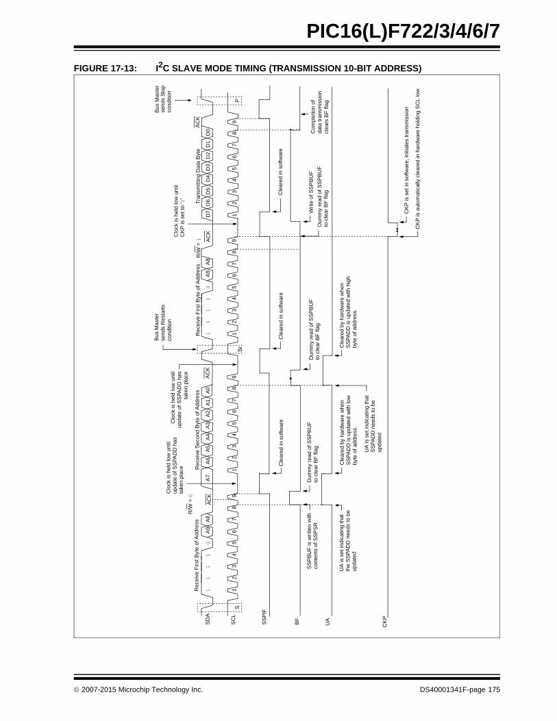
PIC16(L)F722/3/4/6/7
FIGURE 17-13: I2C SLAVE MODE TIMING (TRANSMISSION 10-BIT ADDRESS)
SD
A
SC
L
SS
PIF
BF
S1
23
45
67
89
12
34
56
78
91
23
45
78
9P
11
11
0A
9A
8A
7A
6A
5A
4A
3A
2A
1A
01
11
10
A8
R/W
= 1 A
CK
AC
K
R/W
= 0
AC
K
Re
ceiv
e F
irst
Byt
e o
f Add
ress
Cle
are
d in
so
ftwar
e
Bu
s M
aste
rse
nd
s S
top
con
diti
on
A9
6
Re
ceiv
e S
eco
nd
Byt
e o
f A
dd
ress
Cle
are
d b
y h
ard
wa
re w
hen
SS
PA
DD
is u
pd
ate
d w
ith lo
wb
yte
of
add
ress
.
UA
Clo
ck is
he
ld lo
w u
ntil
upd
ate
of
SS
PA
DD
ha
s ta
ken
pla
ce
UA
is s
et in
dica
ting
tha
tth
e S
SP
AD
D n
ee
ds t
o b
eu
pd
ate
d
UA
is s
et i
nd
ica
ting
tha
tS
SP
AD
D n
ee
ds t
o b
eu
pd
ate
d
Cle
are
d b
y h
ard
wa
re w
he
nS
SP
AD
D is
up
dat
ed
with
hig
hby
te o
f ad
dre
ss.
SS
PB
UF
is w
ritte
n w
ithco
nte
nts
of
SS
PS
RD
um
my
rea
d o
f SS
PB
UF
to c
lea
r B
F fl
ag
Re
ceiv
e F
irst B
yte
of
Ad
dre
ss
12
34
57
89
D7
D6
D5
D4
D3
D1
AC
K
D2
6
Tra
nsm
ittin
g D
ata
Byt
e
D0
Du
mm
y re
ad
of S
SP
BU
Fto
cle
ar
BF
fla
g
Sr
Cle
are
d in
so
ftwa
re
Writ
e o
f S
SP
BU
F
Cle
are
d in
so
ftwa
re
Co
mp
letio
n o
f
cle
ars
BF
fla
g
CK
P
CK
P is
se
t in
softw
are
, in
itia
tes
tra
nsm
issi
on
CK
P is
aut
om
atic
ally
cle
are
d in
ha
rdw
are
ho
ldin
g S
CL
low
Clo
ck is
hel
d lo
w u
ntil
upd
ate
of
SS
PA
DD
ha
sta
ken
pla
ce
dat
a tr
ans
mis
sio
n
Clo
ck is
he
ld lo
w u
ntil
CK
P is
set
to
‘1’
Bu
s M
ast
erse
nds
Res
tart
sco
nd
itio
n
Du
mm
y re
ad
of
SS
PB
UF
to c
lea
r B
F f
lag
2007-2015 Microchip Technology Inc. DS40001341F-page 175

PIC16(L)F722/3/4/6/7
17.2.7 CLOCK STRETCHING
During any SCL low phase, any device on the I2C busmay hold the SCL line low and delay, or pause, thetransmission of data. This “stretching” of a transmissionallows devices to slow down communication on thebus. The SCL line must be constantly sampled by themaster to ensure that all devices on the bus havereleased SCL for more data.
Stretching usually occurs after an ACK bit of atransmission, delaying the first bit of the next byte. TheSSP module hardware automatically stretches for twoconditions:
• After a 10-bit address byte is received (update SSPADD register)
• Anytime the CKP bit of the SSPCON register is cleared by hardware
The module will hold SCL low until the CKP bit is set.This allows the user slave software to update SSPBUFwith data that may not be readily available. In 10-bitaddressing modes, the SSPADD register must beupdated after receiving the first and second addressbytes. The SSP module will hold the SCL line low untilthe SSPADD has a byte written to it. The UA bit of theSSPSTAT register will be set, along with SSPIF,indicating an address update is needed.
17.2.8 FIRMWARE MASTER MODE
Master mode of operation is supported in firmwareusing interrupt generation on the detection of the Startand Stop conditions. The Stop (P) and Start (S) bits ofthe SSPSTAT register are cleared from a Reset orwhen the SSP module is disabled (SSPEN cleared).The Stop (P) and Start (S) bits will toggle based on theStart and Stop conditions. Control of the I2C bus maybe taken when the P bit is set or the bus is Idle and boththe S and P bits are clear.
In Firmware Master mode, the SCL and SDA lines aremanipulated by setting/clearing the corresponding TRISbit(s). The output level is always low, irrespective of thevalue(s) in the corresponding PORT register bit(s).When transmitting a ‘1’, the TRIS bit must be set (input)and a ‘0’, the TRIS bit must be clear (output).
The following events will cause the SSP Interrupt Flagbit, SSPIF, to be set (SSP Interrupt will occur ifenabled):
• Start condition
• Stop condition
• Data transfer byte transmitted/received
Firmware Master Mode of operation can be done witheither the Slave mode Idle (SSPM<3:0> = 1011), orwith either of the Slave modes in which interrupts areenabled. When both master and slave functionality isenabled, the software needs to differentiate thesource(s) of the interrupt.
Refer to Application Note AN554, SoftwareImplementation of I2C™ Bus Master (DS00554) for moreinformation.
17.2.9 MULTI-MASTER MODE
In Multi-Master mode, the interrupt generation on thedetection of the Start and Stop conditions allow thedetermination of when the bus is free. The Stop (P) andStart (S) bits are cleared from a Reset or when the SSPmodule is disabled. The Stop (P) and Start (S) bits willtoggle based on the Start and Stop conditions. Controlof the I2C bus may be taken when the P bit of theSSPSTAT register is set or when the bus is Idle, andboth the S and P bits are clear. When the bus is busy,enabling the SSP Interrupt will generate the interruptwhen the Stop condition occurs.
In Multi-Master operation, the SDA line must bemonitored to see if the signal level is the expectedoutput level. This check only needs to be done when ahigh level is output. If a high level is expected and a lowlevel is present, the device needs to release the SDAand SCL lines (set TRIS bits). There are two stageswhere this arbitration of the bus can be lost. They arethe Address Transfer and Data Transfer stages.
When the slave logic is enabled, the slave continues toreceive. If arbitration was lost during the addresstransfer stage, communication to the device may be inprogress. If addressed, an ACK pulse will begenerated. If arbitration was lost during the datatransfer stage, the device will need to re-transfer thedata at a later time.
Refer to Application Note AN578, Use of the SSPModule in the I2C™ Multi-Master Environment(DS00578) for more information.
DS40001341F-page 176 2007-2015 Microchip Technology Inc.

PIC16(L)F722/3/4/6/7
17.2.10 CLOCK SYNCHRONIZATION
When the CKP bit is cleared, the SCL output is held lowonce it is sampled low. therefore, the CKP bit will notstretch the SCL line until an external I2C master devicehas already asserted the SCL line low. The SCL outputwill remain low until the CKP bit is set and all otherdevices on the I2C bus have released SCL. Thisensures that a write to the CKP bit will not violate theminimum high time requirement for SCL(Figure 17-14).
17.2.11 SLEEP OPERATION
While in Sleep mode, the I2C module can receiveaddresses of data, and when an address match orcomplete byte transfer occurs, wake the processorfrom Sleep (if SSP interrupt is enabled).
FIGURE 17-14: CLOCK SYNCHRONIZATION TIMING
SDA
SCL
DX-1DX
WR
Q1 Q2 Q3 Q4 Q1 Q2 Q3 Q4 Q1 Q2 Q3 Q4 Q1 Q2 Q3 Q4 Q1 Q2 Q3 Q4 Q1 Q2 Q3 Q4 Q1 Q2 Q3 Q4
SSPCON
CKP
Master devicedeasserts clock
Master deviceasserts clock
2007-2015 Microchip Technology Inc. DS40001341F-page 177

PIC16(L)F722/3/4/6/7
REGISTER 17-3: SSPCON: SYNCHRONOUS SERIAL PORT CONTROL REGISTER (I2C MODE)
R/W-0 R/W-0 R/W-0 R/W-0 R/W-0 R/W-0 R/W-0 R/W-0
WCOL SSPOV SSPEN CKP SSPM3 SSPM2 SSPM1 SSPM0
bit 7 bit 0
Legend:
R = Readable bit W = Writable bit U = Unimplemented bit, read as ‘0’
-n = Value at POR ‘1’ = Bit is set ‘0’ = Bit is cleared x = Bit is unknown
bit 7 WCOL: Write Collision Detect bit
1 = The SSPBUF register is written while it is still transmitting the previous word (must be cleared insoftware)
0 = No collision
bit 6 SSPOV: Receive Overflow Indicator bit
1 = A byte is received while the SSPBUF register is still holding the previous byte. SSPOV is a “don’tcare” in Transmit mode. SSPOV must be cleared in software in either mode.
0 = No overflow
bit 5 SSPEN: Synchronous Serial Port Enable bit
1 = Enables the serial port and configures the SDA and SCL pins as serial port pins(2)
0 = Disables serial port and configures these pins as I/O port pins
bit 4 CKP: Clock Polarity Select bit
1 = Release control of SCL0 = Holds clock low (clock stretch). (Used to ensure data setup time.)
bit 3-0 SSPM<3:0>: Synchronous Serial Port Mode Select bits
0110 = I2C Slave mode, 7-bit address0111 = I2C Slave mode, 10-bit address1000 = Reserved1001 = Load SSPMSK register at SSPADD SFR Address(1)
1010 = Reserved1011 = I2C Firmware Controlled Master mode (Slave Idle)1100 = Reserved1101 = Reserved1110 = I2C Slave mode, 7-bit address with Start and Stop bit interrupts enabled1111 = I2C Slave mode, 10-bit address with Start and Stop bit interrupts enabled
Note 1: When this mode is selected, any reads or writes to the SSPADD SFR address accesses the SSPMSK register.
2: When enabled, these pins must be properly configured as input or output using the associated TRIS bit.
DS40001341F-page 178 2007-2015 Microchip Technology Inc.

PIC16(L)F722/3/4/6/7
REGISTER 17-4: SSPSTAT: SYNCHRONOUS SERIAL PORT STATUS REGISTER (I2C MODE)
R/W-0 R/W-0 R-0 R-0 R-0 R-0 R-0 R-0
SMP CKE D/A P S R/W UA BF
bit 7 bit 0
Legend:
R = Readable bit W = Writable bit U = Unimplemented bit, read as ‘0’
-n = Value at POR ‘1’ = Bit is set ‘0’ = Bit is cleared x = Bit is unknown
bit 7 SMP: SPI Data Input Sample Phase bit1 = Slew Rate Control (limiting) disabled. Operating in I2C Standard Mode (100 kHz and 1 MHz).0 = Slew Rate Control (limiting) enabled. Operating in I2C Fast Mode (400 kHz).
bit 6 CKE: SPI Clock Edge Select bitThis bit must be maintained clear. Used in SPI mode only.
bit 5 D/A: DATA/ADDRESS bit (I2C mode only)1 = Indicates that the last byte received or transmitted was data0 = Indicates that the last byte received or transmitted was address
bit 4 P: Stop bitThis bit is cleared when the SSP module is disabled, or when the Start bit is detected last.1 = Indicates that a Stop bit has been detected last (this bit is ‘0’ on Reset)0 = Stop bit was not detected last
bit 3 S: Start bitThis bit is cleared when the SSP module is disabled, or when the Stop bit is detected last.1 = Indicates that a Start bit has been detected last (this bit is ‘0’ on Reset)0 = Start bit was not detected last
bit 2 R/W: READ/WRITE bit InformationThis bit holds the R/W bit information following the last address match. This bit is only valid from the address match to the next Start bit, Stop bit or ACK bit.1 = Read0 = Write
bit 1 UA: Update Address bit (10-bit I2C mode only)1 = Indicates that the user needs to update the address in the SSPADD register0 = Address does not need to be updated
bit 0 BF: Buffer Full Status bitReceive:1 = Receive complete, SSPBUF is full0 = Receive not complete, SSPBUF is emptyTransmit:1 = Transmit in progress, SSPBUF is full0 = Transmit complete, SSPBUF is empty
2007-2015 Microchip Technology Inc. DS40001341F-page 179

PIC16(L)F722/3/4/6/7
TABLE 17-7: REGISTERS ASSOCIATED WITH I2C OPERATION
REGISTER 17-5: SSPMSK: SSP MASK REGISTER
R/W-1 R/W-1 R/W-1 R/W-1 R/W-1 R/W-1 R/W-1 R/W-1
MSK7 MSK6 MSK5 MSK4 MSK3 MSK2 MSK1 MSK0
bit 7 bit 0
Legend:
R = Readable bit W = Writable bit U = Unimplemented bit, read as ‘0’
-n = Value at POR ‘1’ = Bit is set ‘0’ = Bit is cleared x = Bit is unknown
bit 7-1 MSK<7:1>: Mask bits1 = The received address bit n is compared to SSPADD<n> to detect I2C address match0 = The received address bit n is not used to detect I2C address match
bit 0 MSK<0>: Mask bit for I2C Slave Mode, 10-bit AddressI2C Slave Mode, 10-bit Address (SSPM<3:0> = 0111):1 = The received address bit ‘0’ is compared to SSPADD<0> to detect I2C address match0 = The received address bit ‘0’ is not used to detect I2C address matchAll other SSP modes: this bit has no effect.
REGISTER 17-6: SSPADD: SSP I2C ADDRESS REGISTER
R/W-0 R/W-0 R/W-0 R/W-0 R/W-0 R/W-0 R/W-0 R/W-0
ADD7 ADD6 ADD5 ADD4 ADD3 ADD2 ADD1 ADD0
bit 7 bit 0
Legend:
R = Readable bit W = Writable bit U = Unimplemented bit, read as ‘0’
-n = Value at POR ‘1’ = Bit is set ‘0’ = Bit is cleared x = Bit is unknown
bit 7-0 ADD<7:0>: Address bitsReceived address
Name Bit 7 Bit 6 Bit 5 Bit 4 Bit 3 Bit 2 Bit 1 Bit 0Value on
POR, BOR
Value on all other Resets
INTCON GIE PEIE T0IE INTE RBIE T0IF INTF RBIF 0000 000x 0000 000u
PIR1 TMR1GIF ADIF RCIF TXIF SSPIF CCP1IF TMR2IF TMR1IF 0000 0000 0000 0000
PIE1 TMR1GIE ADIE RCIE TXIE SSPIE CCP1IE TMR2IE TMR1IE 0000 0000 0000 0000
SSPBUF Synchronous Serial Port Receive Buffer/Transmit Register xxxx xxxx uuuu uuuu
SSPADD Synchronous Serial Port (I2C mode) Address Register 0000 0000 0000 0000
SSPCON WCOL SSPOV SSPEN CKP SSPM3 SSPM2 SSPM1 SSPM0 0000 0000 0000 0000
SSPMSK(2) Synchronous Serial Port (I2C mode) Address Mask Register 1111 1111 1111 1111
SSPSTAT SMP(1) CKE(1) D/A P S R/W UA BF 0000 0000 0000 0000
TRISC TRISC7 TRISC6 TRISC5 TRISC4 TRISC3 TRISC2 TRISC1 TRISC0 1111 1111 1111 1111
Legend: x = unknown, u = unchanged, - = unimplemented locations read as ‘0’. Shaded cells are not used by SSP module in I2C mode.
Note 1: Maintain these bits clear in I2C mode.2: Accessible only when SSPM<3:0> = 1001.
DS40001341F-page 180 2007-2015 Microchip Technology Inc.
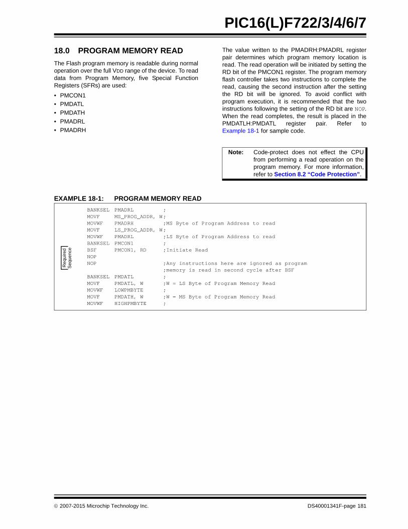
PIC16(L)F722/3/4/6/7
18.0 PROGRAM MEMORY READ
The Flash program memory is readable during normaloperation over the full VDD range of the device. To readdata from Program Memory, five Special FunctionRegisters (SFRs) are used:
• PMCON1
• PMDATL
• PMDATH
• PMADRL
• PMADRH
The value written to the PMADRH:PMADRL registerpair determines which program memory location isread. The read operation will be initiated by setting theRD bit of the PMCON1 register. The program memoryflash controller takes two instructions to complete theread, causing the second instruction after the settingthe RD bit will be ignored. To avoid conflict withprogram execution, it is recommended that the twoinstructions following the setting of the RD bit are NOP.When the read completes, the result is placed in thePMDATLH:PMDATL register pair. Refer toExample 18-1 for sample code.
EXAMPLE 18-1: PROGRAM MEMORY READ
Note: Code-protect does not effect the CPUfrom performing a read operation on theprogram memory. For more information,refer to Section 8.2 “Code Protection”.
BANKSEL PMADRL ;MOVF MS_PROG_ADDR, W;MOVWF PMADRH ;MS Byte of Program Address to readMOVF LS_PROG_ADDR, W;MOVWF PMADRL ;LS Byte of Program Address to readBANKSEL PMCON1 ;BSF PMCON1, RD ;Initiate ReadNOPNOP ;Any instructions here are ignored as program
;memory is read in second cycle after BSFBANKSEL PMDATL ;MOVF PMDATL, W ;W = LS Byte of Program Memory ReadMOVWF LOWPMBYTE ;MOVF PMDATH, W ;W = MS Byte of Program Memory ReadMOVWF HIGHPMBYTE ;
Re
quire
dS
equ
ence
2007-2015 Microchip Technology Inc. DS40001341F-page 181

PIC16(L)F722/3/4/6/7
REGISTER 18-1: PMCON1: PROGRAM MEMORY CONTROL 1 REGISTER
R-1 U-0 U-0 U-0 U-0 U-0 U-0 R/S-0
Reserved — —l — — — — RD
bit 7 bit 0
Legend: S = Setable bit, cleared in hardware
R = Readable bit W = Writable bit U = Unimplemented bit, read as ‘0’
-n = Value at POR ‘1’ = Bit is set ‘0’ = Bit is cleared x = Bit is unknown
bit 7 Reserved: Read as ‘1’. Maintain this bit set.
bit 6-1 Unimplemented: Read as ‘0’
bit 0 RD: Read Control bit
1 = Initiates an program memory read (The RD is cleared in hardware; the RD bit can only be set (notcleared) in software).
0 = Does not initiate a program memory read
REGISTER 18-2: PMDATH: PROGRAM MEMORY DATA HIGH REGISTER
U-0 U-0 R/W-x R/W-x R/W-x R/W-x R/W-x R/W-x
— — PMD13 PMD12 PMD11 PMD10 PMD9 PMD8
bit 7 bit 0
Legend:
R = Readable bit W = Writable bit U = Unimplemented bit, read as ‘0’
-n = Value at POR ‘1’ = Bit is set ‘0’ = Bit is cleared x = Bit is unknown
bit 7-6 Unimplemented: Read as ‘0’
bit 5-0 PMD<13:8>: The value of the program memory word pointed to by PMADRH and PMADRL after a program memory read command.
REGISTER 18-3: PMDATL: PROGRAM MEMORY DATA LOW REGISTER
R/W-x R/W-x R/W-x R/W-x R/W-x R/W-x R/W-x R/W-x
PMD7 PMD6 PMD5 PMD4 PMD3 PMD2 PMD1 PMD0
bit 7 bit 0
Legend:
R = Readable bit W = Writable bit U = Unimplemented bit, read as ‘0’
-n = Value at POR ‘1’ = Bit is set ‘0’ = Bit is cleared x = Bit is unknown
bit 7-0 PMD<7:0>: The value of the program memory word pointed to by PMADRH and PMADRL after a program memory read command.
DS40001341F-page 182 2007-2015 Microchip Technology Inc.

PIC16(L)F722/3/4/6/7
TABLE 18-1: SUMMARY OF REGISTERS ASSOCIATED WITH PROGRAM MEMORY READ
REGISTER 18-4: PMADRH: PROGRAM MEMORY ADDRESS HIGH REGISTER
U-0 U-0 U-0 R/W-x R/W-x R/W-x R/W-x R/W-x
— — — PMA12 PMA11 PMA10 PMA9 PMA8
bit 7 bit 0
Legend:
R = Readable bit W = Writable bit U = Unimplemented bit, read as ‘0’
-n = Value at POR ‘1’ = Bit is set ‘0’ = Bit is cleared x = Bit is unknown
bit 7-5 Unimplemented: Read as ‘0’
bit 4-0 PMA<12:8>: Program Memory Read Address bits
REGISTER 18-5: PMADRL: PROGRAM MEMORY ADDRESS LOW REGISTER
R/W-x R/W-x R/W-x R/W-x R/W-x R/W-x R/W-x R/W-x
PMA7 PMA6 PMA5 PMA4 PMA3 PMA2 PMA1 PMA0
bit 7 bit 0
Legend:
R = Readable bit W = Writable bit U = Unimplemented bit, read as ‘0’
-n = Value at POR ‘1’ = Bit is set ‘0’ = Bit is cleared x = Bit is unknown
bit 7-0 PMA<7:0>: Program Memory Read Address bits
Name Bit 7 Bit 6 Bit 5 Bit 4 Bit 3 Bit 2 Bit 1 Bit 0Value on
POR, BORValue on all other Resets
PMCON1 Reserved — — — — — — RD 1--- ---0 1--- ---0
PMADRH — — — Program Memory Read Address Register High Byte ---x xxxx ---x xxxx
PMADRL Program Memory Read Address Register Low Byte xxxx xxxx xxxx xxxx
PMDATH — — Program Memory Read Data Register High Byte --xx xxxx --xx xxxx
PMDATL Program Memory Read Data Register Low Byte xxxx xxxx xxxx xxxx
Legend: x = unknown, u = unchanged, – = unimplemented, read as ‘0’. Shaded cells are not used by the Program Memory Read.
2007-2015 Microchip Technology Inc. DS40001341F-page 183
PIC16(L)F722/3/4/6/7
19.0 POWER-DOWN MODE (SLEEP)
The Power-down mode is entered by executing aSLEEP instruction.
If the Watchdog Timer is enabled:
• WDT will be cleared but keeps running.
• PD bit of the STATUS register is cleared.
• TO bit of the STATUS register is set.
• Oscillator driver is turned off.
• Timer1 oscillator is unaffected
• I/O ports maintain the status they had before SLEEP was executed (driving high, low or high-impedance).
For lowest current consumption in this mode, all I/Opins should be either at VDD or VSS, with no externalcircuitry drawing current from the I/O pin. I/O pins thatare high-impedance inputs should be pulled high or lowexternally to avoid switching currents caused by float-ing inputs. The T0CKI input should also be at VDD orVSS for lowest current consumption. The contributionfrom on-chip pull-ups on PORTB should be considered.
The MCLR pin must be at a logic high level whenexternal MCLR is enabled.
19.1 Wake-up from Sleep
The device can wake up from Sleep through one of thefollowing events:
1. External Reset input on MCLR pin.
2. Watchdog Timer wake-up (if WDT wasenabled).
3. Interrupt from RB0/INT pin, PORTB change or aperipheral interrupt.
The first event will cause a device Reset. The two latterevents are considered a continuation of programexecution. The TO and PD bits in the STATUS registercan be used to determine the cause of device Reset.The PD bit, which is set on power-up, is cleared whenSleep is invoked. TO bit is cleared if WDT wake-upoccurred.
The following peripheral interrupts can wake the devicefrom Sleep:
1. TMR1 Interrupt. Timer1 must be operating as anasynchronous counter.
2. USART Receive Interrupt (Synchronous Slavemode only)
3. A/D conversion (when A/D clock source is RC)
4. Interrupt-on-change
5. External Interrupt from INT pin
6. Capture event on CCP1 or CCP2
7. SSP Interrupt in SPI or I2C Slave mode
Other peripherals cannot generate interrupts sinceduring Sleep, no on-chip clocks are present.
When the SLEEP instruction is being executed, the nextinstruction (PC + 1) is prefetched. For the device towake-up through an interrupt event, the correspondinginterrupt enable bit must be set (enabled). Wake-up isregardless of the state of the GIE bit. If the GIE bit isclear (disabled), the device continues execution at theinstruction after the SLEEP instruction. If the GIE bit isset (enabled), the device executes the instruction afterthe SLEEP instruction, then branches to the interruptaddress (0004h). In cases where the execution of theinstruction following SLEEP is not desirable, the usershould have a NOP after the SLEEP instruction.
The WDT is cleared when the device wakes up fromSleep, regardless of the source of wake-up.
Note: A Reset generated by a WDT time outdoes not drive MCLR pin low.
Note: If the global interrupts are disabled (GIE iscleared), but any interrupt source has bothits interrupt enable bit and the correspond-ing interrupt flag bits set, the device willimmediately wake-up from Sleep. TheSLEEP instruction is completely executed.
DS40001341F-page 184 2007-2015 Microchip Technology Inc.

PIC16(L)F722/3/4/6/7
19.2 Wake-up Using Interrupts
When global interrupts are disabled (GIE cleared) andany interrupt source has both its interrupt enable bitand interrupt flag bit set, one of the following will occur:
• If the interrupt occurs before the execution of a SLEEP instruction, the SLEEP instruction will complete as a NOP. Therefore, the WDT and WDT prescaler and postscaler (if enabled) will not be cleared, the TO bit will not be set and the PD bit will not be cleared.
• If the interrupt occurs during or after the execution of a SLEEP instruction, the device will immediately wake-up from Sleep. The SLEEP instruction will be completely executed before the wake-up. Therefore, the WDT and WDT prescaler and postscaler (if enabled) will be cleared, the TO bit will be set and the PD bit will be cleared.
Even if the flag bits were checked before executing aSLEEP instruction, it may be possible for flag bits tobecome set before the SLEEP instruction completes. Todetermine whether a SLEEP instruction executed, testthe PD bit. If the PD bit is set, the SLEEP instructionwas executed as a NOP.
To ensure that the WDT is cleared, a CLRWDT instructionshould be executed before a SLEEP instruction.
FIGURE 19-1: WAKE-UP FROM SLEEP THROUGH INTERRUPT
TABLE 19-1: SUMMARY OF REGISTERS ASSOCIATED WITH POWER-DOWN MODE
Name Bit 7 Bit 6 Bit 5 Bit 4 Bit 3 Bit 2 Bit 1 Bit 0Value on
POR, BORValue on all other Resets
IOCB IOCB7 IOCB6 IOCB5 IOCB4 IOCB3 IOCB2 IOCB1 IOCB0 0000 0000 0000 0000
INTCON GIE PEIE T0IE INTE RBIE T0IF INTF RBIF 0000 0000 0000 0000
PIE1 TMR1GIE ADIE RCIE TXIE SSPIE CCP1IE TMR2IE TMR1IE 0000 0000 0000 0000
PIE2 — — — — — — — CCP2IE ---- ---0 ---- ---0
PIR1 TMR1GIF ADIF RCIF TXIF SSPIF CCP1IF TMR2IF TMR1IF 0000 0000 0000 0000
PIR2 — — — — — — — CCP2IF ---- ---0 ---- ---0
Legend: x = unknown, u = unchanged, – = unimplemented, read as ‘0’. Shaded cells are not used in Power-Down mode.
Q1 Q2 Q3 Q4 Q1 Q2 Q3 Q4 Q1 Q1 Q2 Q3 Q4 Q1 Q2 Q3 Q4 Q1 Q2 Q3 Q4 Q1 Q2 Q3 Q4
OSC1(1)
CLKOUT(4)
INT pin
INTF flag(INTCON reg.)
GIE bit(INTCON reg.)
Instruction FlowPC
InstructionFetched
InstructionExecuted
PC PC + 1 PC + 2
Inst(PC) = Sleep
Inst(PC - 1)
Inst(PC + 1)
Sleep
Processor inSleep
Interrupt Latency(3)
Inst(PC + 2)
Inst(PC + 1)
Inst(0004h) Inst(0005h)
Inst(0004h)Dummy Cycle
PC + 2 0004h 0005h
Dummy Cycle
TOST(2)
PC + 2
Note 1: XT, HS or LP Oscillator mode assumed.2: TOST = 1024 TOSC (drawing not to scale). This delay does not apply to EC and RC Oscillator modes.3: GIE = 1 assumed. In this case after wake-up, the processor jumps to 0004h. If GIE = 0, execution will continue in-line.4: CLKOUT is not available in XT, HS, LP or EC Oscillator modes, but shown here for timing reference.
2007-2015 Microchip Technology Inc. DS40001341F-page 185

PIC16(L)F722/3/4/6/7
DS40001341F-page 186 2007-2015 Microchip Technology Inc.
20.0 IN-CIRCUIT SERIAL PROGRAMMING™ (ICSP™)
ICSP™ programming allows customers to manufacturecircuit boards with unprogrammed devices. Programmingcan be done after the assembly process allowing thedevice to be programmed with the most recent firmwareor a custom firmware. Five pins are needed for ICSP™programming:
• ICSPCLK
• ICSPDAT
• MCLR/VPP
• VDD
• VSS
The device is placed into Program/Verify mode byholding the ICSPCLK and ICSPDAT pins low thenraising the voltage on MCLR/VPP from 0v to VPP. InProgram/Verify mode the program memory, User IDsand the Configuration Words are programmed throughserial communications. The ICSPDAT pin is abidirectional I/O used for transferring the serial data andthe ISCPCLK pin is the clock input. For more informationon ICSP, refer to the “PIC16(L)F72x MemoryProgramming Specification” (DS41332).
FIGURE 20-1: TYPICAL CONNECTION FOR ICSP™ PROGRAMMING
Note: The ICD 2 produces a VPP voltage greaterthan the maximum VPP specification of thePIC16(L)F722/3/4/6/7. When using thisprogrammer, an external circuit, such asthe AC164112 MPLAB ICD 2 VPP voltagelimiter, is required to keep the VPP voltagewithin the device specifications.
VDD
VPP
GND
ExternalDevice to be
Data
Clock
VDD
MCLR/VPP
VSS
ICSPDAT
ICSPCLK
* **
To Normal Connections
* Isolation devices (as required).
10k
Programming Signals Programmed
VDD

PIC16(L)F722/3/4/6/7
21.0 INSTRUCTION SET SUMMARY
The PIC16(L)F722/3/4/6/7 instruction set is highlyorthogonal and is comprised of three basic categories:
• Byte-oriented operations
• Bit-oriented operations
• Literal and control operations
Each PIC16 instruction is a 14-bit word divided into anopcode, which specifies the instruction type and one ormore operands, which further specify the operation ofthe instruction. The formats for each of the categoriesis presented in Figure 21-1, while the various opcodefields are summarized in Table 21-1.
Table 21-2 lists the instructions recognized by theMPASMTM assembler.
For byte-oriented instructions, ‘f’ represents a fileregister designator and ‘d’ represents a destinationdesignator. The file register designator specifies whichfile register is to be used by the instruction.
The destination designator specifies where the result ofthe operation is to be placed. If ‘d’ is zero, the result isplaced in the W register. If ‘d’ is one, the result is placedin the file register specified in the instruction.
For bit-oriented instructions, ‘b’ represents a bit fielddesignator, which selects the bit affected by theoperation, while ‘f’ represents the address of the file inwhich the bit is located.
For literal and control operations, ‘k’ represents an8-bit or 11-bit constant, or literal value.
One instruction cycle consists of four oscillator periods;for an oscillator frequency of 4 MHz, this gives anominal instruction execution time of 1 s. Allinstructions are executed within a single instructioncycle, unless a conditional test is true, or the programcounter is changed as a result of an instruction. Whenthis occurs, the execution takes two instruction cycles,with the second cycle executed as a NOP.
All instruction examples use the format ‘0xhh’ torepresent a hexadecimal number, where ‘h’ signifies ahexadecimal digit.
21.1 Read-Modify-Write Operations
Any instruction that specifies a file register as part ofthe instruction performs a Read-Modify-Write (R-M-W)operation. The register is read, the data is modified,and the result is stored according to either the instruc-tion, or the destination designator ‘d’. A read operationis performed on a register even if the instruction writesto that register.
For example, a CLRF PORTB instruction will readPORTB, clear all the data bits, then write the resultback to PORTB. This example would have theunintended consequence of clearing the condition thatset the RBIF flag.
TABLE 21-1: OPCODE FIELD DESCRIPTIONS
FIGURE 21-1: GENERAL FORMAT FOR INSTRUCTIONS
Field Description
f Register file address (0x00 to 0x7F)
W Working register (accumulator)
b Bit address within an 8-bit file register
k Literal field, constant data or label
x Don’t care location (= 0 or 1). The assembler will generate code with x = 0. It is the recommended form of use for compatibility with all Microchip software tools.
d Destination select; d = 0: store result in W,d = 1: store result in file register f. Default is d = 1.
PC Program Counter
TO Time-out bit
C Carry bit
DC Digit carry bit
Z Zero bit
PD Power-down bit
Byte-oriented file register operations13 8 7 6 0
d = 0 for destination W
OPCODE d f (FILE #)
d = 1 for destination ff = 7-bit file register address
Bit-oriented file register operations13 10 9 7 6 0
OPCODE b (BIT #) f (FILE #)
b = 3-bit bit addressf = 7-bit file register address
Literal and control operations
13 8 7 0
OPCODE k (literal)
k = 8-bit immediate value
13 11 10 0
OPCODE k (literal)
k = 11-bit immediate value
General
CALL and GOTO instructions only
2007-2015 Microchip Technology Inc. DS40001341F-page 187

PIC16(L)F722/3/4/6/7
TABLE 21-2: PIC16(L)F722/3/4/6/7 INSTRUCTION SET
Mnemonic,Operands
Description Cycles14-Bit Opcode Status
AffectedNotes
MSb LSb
BYTE-ORIENTED FILE REGISTER OPERATIONS
ADDWFANDWFCLRFCLRWCOMFDECFDECFSZINCFINCFSZIORWFMOVFMOVWFNOPRLFRRFSUBWFSWAPFXORWF
f, df, d
f–
f, df, df, df, df, df, df, d
f–
f, df, df, df, df, d
Add W and fAND W with fClear fClear WComplement fDecrement fDecrement f, Skip if 0Increment fIncrement f, Skip if 0Inclusive OR W with fMove fMove W to fNo OperationRotate Left f through CarryRotate Right f through CarrySubtract W from fSwap nibbles in fExclusive OR W with f
111111
1(2)1
1(2)111111111
000000000000000000000000000000000000
011101010001000110010011101110101111010010000000000011011100001011100110
dfffdffflfff0xxxdfffdfffdfffdfffdfffdfffdffflfff0xx0dfffdfffdfffdfffdfff
ffffffffffffxxxxffffffffffffffffffffffffffffffff0000ffffffffffffffffffff
C, DC, ZZZZZZ
Z
ZZ
CC
C, DC, Z
Z
1, 21, 2
2
1, 21, 2
1, 2, 31, 2
1, 2, 31, 21, 2
1, 21, 21, 21, 21, 2
BIT-ORIENTED FILE REGISTER OPERATIONS
BCFBSFBTFSCBTFSS
f, bf, bf, bf, b
Bit Clear fBit Set fBit Test f, Skip if ClearBit Test f, Skip if Set
11
1 (2)1 (2)
01010101
00bb01bb10bb11bb
bfffbfffbfffbfff
ffffffffffffffff
1, 21, 2
33
LITERAL AND CONTROL OPERATIONS
ADDLWANDLWCALLCLRWDTGOTOIORLWMOVLWRETFIERETLWRETURNSLEEPSUBLWXORLW
kkk–kkk–k––kk
Add literal and WAND literal with WCall SubroutineClear Watchdog TimerGo to addressInclusive OR literal with WMove literal to WReturn from interruptReturn with literal in WReturn from SubroutineGo into Standby modeSubtract W from literalExclusive OR literal with W
1121211222111
11111000101111001100001111
111x10010kkk00001kkk100000xx000001xx00000000110x1010
kkkkkkkkkkkk0110kkkkkkkkkkkk0000kkkk00000110kkkkkkkk
kkkkkkkkkkkk0100kkkkkkkkkkkk1001kkkk10000011kkkkkkkk
C, DC, ZZ
TO, PD
Z
TO, PDC, DC, Z
Z
Note 1: When an I/O register is modified as a function of itself (e.g., MOVF PORTA, 1), the value used will be that value present on the pins themselves. For example, if the data latch is ‘1’ for a pin configured as input and is driven low by an external device, the data will be written back with a ‘0’.
2: If this instruction is executed on the TMR0 register (and where applicable, d = 1), the prescaler will be cleared if assigned to the Timer0 module.
3: If the Program Counter (PC) is modified, or a conditional test is true, the instruction requires two cycles. The second cycle is executed as a NOP.
DS40001341F-page 188 2007-2015 Microchip Technology Inc.

PIC16(L)F722/3/4/6/7
21.2 Instruction Descriptions
ADDLW Add literal and W
Syntax: [ label ] ADDLW k
Operands: 0 k 255
Operation: (W) + k (W)
Status Affected: C, DC, Z
Description: The contents of the W register are added to the 8-bit literal ‘k’ and the result is placed in the W register.
ADDWF Add W and f
Syntax: [ label ] ADDWF f,d
Operands: 0 f 127d 0,1
Operation: (W) + (f) (destination)
Status Affected: C, DC, Z
Description: Add the contents of the W register with register ‘f’. If ‘d’ is ‘0’, the result is stored in the W register. If ‘d’ is ‘1’, the result is stored back in register ‘f’.
ANDLW AND literal with W
Syntax: [ label ] ANDLW k
Operands: 0 k 255
Operation: (W) .AND. (k) (W)
Status Affected: Z
Description: The contents of W register are AND’ed with the 8-bit literal ‘k’. The result is placed in the W reg-ister.
ANDWF AND W with f
Syntax: [ label ] ANDWF f,d
Operands: 0 f 127d 0,1
Operation: (W) .AND. (f) (destination)
Status Affected: Z
Description: AND the W register with register ‘f’. If ‘d’ is ‘0’, the result is stored in the W register. If ‘d’ is ‘1’, the result is stored back in register ‘f’.
BCF Bit Clear f
Syntax: [ label ] BCF f,b
Operands: 0 f 1270 b 7
Operation: 0 (f<b>)
Status Affected: None
Description: Bit ‘b’ in register ‘f’ is cleared.
BSF Bit Set f
Syntax: [ label ] BSF f,b
Operands: 0 f 1270 b 7
Operation: 1 (f<b>)
Status Affected: None
Description: Bit ‘b’ in register ‘f’ is set.
BTFSC Bit Test f, Skip if Clear
Syntax: [ label ] BTFSC f,b
Operands: 0 f 1270 b 7
Operation: skip if (f<b>) = 0
Status Affected: None
Description: If bit ‘b’ in register ‘f’ is ‘1’, the next instruction is executed.If bit ‘b’, in register ‘f’, is ‘0’, the next instruction is discarded, and a NOP is executed instead, making this a 2-cycle instruction.
2007-2015 Microchip Technology Inc. DS40001341F-page 189

PIC16(L)F722/3/4/6/7
BTFSS Bit Test f, Skip if Set
Syntax: [ label ] BTFSS f,b
Operands: 0 f 1270 b < 7
Operation: skip if (f<b>) = 1
Status Affected: None
Description: If bit ‘b’ in register ‘f’ is ‘0’, the next instruction is executed.If bit ‘b’ is ‘1’, then the nextinstruction is discarded and a NOP is executed instead, making this a 2-cycle instruction.
CALL Call Subroutine
Syntax: [ label ] CALL k
Operands: 0 k 2047
Operation: (PC)+ 1 TOS,k PC<10:0>,(PCLATH<4:3>) PC<12:11>
Status Affected: None
Description: Call Subroutine. First, return address (PC + 1) is pushed onto the stack. The 11-bit immediate address is loaded into PC bits <10:0>. The upper bits of the PC are loaded from PCLATH. CALL is a 2-cycle instruction.
CLRF Clear f
Syntax: [ label ] CLRF f
Operands: 0 f 127
Operation: 00h (f)1 Z
Status Affected: Z
Description: The contents of register ‘f’ are cleared and the Z bit is set.
CLRW Clear W
Syntax: [ label ] CLRW
Operands: None
Operation: 00h (W)1 Z
Status Affected: Z
Description: W register is cleared. Zero bit (Z) is set.
CLRWDT Clear Watchdog Timer
Syntax: [ label ] CLRWDT
Operands: None
Operation: 00h WDT0 WDT prescaler,1 TO1 PD
Status Affected: TO, PD
Description: CLRWDT instruction resets the Watchdog Timer. It also resets the prescaler of the WDT. Status bits TO and PD are set.
COMF Complement f
Syntax: [ label ] COMF f,d
Operands: 0 f 127d [0,1]
Operation: (f) (destination)
Status Affected: Z
Description: The contents of register ‘f’ are complemented. If ‘d’ is ‘0’, the result is stored in W. If ‘d’ is ‘1’, the result is stored back inregister ‘f’.
DECF Decrement f
Syntax: [ label ] DECF f,d
Operands: 0 f 127d [0,1]
Operation: (f) - 1 (destination)
Status Affected: Z
Description: Decrement register ‘f’. If ‘d’ is ‘0’, the result is stored in the W register. If ‘d’ is ‘1’, the result is stored back in register ‘f’.
DS40001341F-page 190 2007-2015 Microchip Technology Inc.

PIC16(L)F722/3/4/6/7
DECFSZ Decrement f, Skip if 0
Syntax: [ label ] DECFSZ f,d
Operands: 0 f 127d [0,1]
Operation: (f) - 1 (destination); skip if result = 0
Status Affected: None
Description: The contents of register ‘f’ are decremented. If ‘d’ is ‘0’, the result is placed in the W register. If ‘d’ is ‘1’, the result is placed back in register ‘f’. If the result is ‘1’, the next instruction is executed. If the result is ‘0’, then a NOP is executed instead, making it a 2-cycle instruction.
GOTO Unconditional Branch
Syntax: [ label ] GOTO k
Operands: 0 k 2047
Operation: k PC<10:0>PCLATH<4:3> PC<12:11>
Status Affected: None
Description: GOTO is an unconditional branch. The 11-bit immediate value is loaded into PC bits <10:0>. The upper bits of PC are loaded from PCLATH<4:3>. GOTO is a 2-cycle instruction.
INCF Increment f
Syntax: [ label ] INCF f,d
Operands: 0 f 127d [0,1]
Operation: (f) + 1 (destination)
Status Affected: Z
Description: The contents of register ‘f’ are incremented. If ‘d’ is ‘0’, the result is placed in the W register. If ‘d’ is ‘1’, the result is placed back in register ‘f’.
INCFSZ Increment f, Skip if 0
Syntax: [ label ] INCFSZ f,d
Operands: 0 f 127d [0,1]
Operation: (f) + 1 (destination), skip if result = 0
Status Affected: None
Description: The contents of register ‘f’ are incremented. If ‘d’ is ‘0’, the result is placed in the W register. If ‘d’ is ‘1’, the result is placed back in register ‘f’.If the result is ‘1’, the next instruction is executed. If the result is ‘0’, a NOP is executed instead, making it a 2-cycle instruction.
IORLW Inclusive OR literal with W
Syntax: [ label ] IORLW k
Operands: 0 k 255
Operation: (W) .OR. k (W)
Status Affected: Z
Description: The contents of the W register are OR’ed with the 8-bit literal ‘k’. The result is placed in the W register.
IORWF Inclusive OR W with f
Syntax: [ label ] IORWF f,d
Operands: 0 f 127d [0,1]
Operation: (W) .OR. (f) (destination)
Status Affected: Z
Description: Inclusive OR the W register with register ‘f’. If ‘d’ is ‘0’, the result is placed in the W register. If ‘d’ is ‘1’, the result is placed back in register ‘f’.
2007-2015 Microchip Technology Inc. DS40001341F-page 191

PIC16(L)F722/3/4/6/7
MOVF Move f
Syntax: [ label ] MOVF f,d
Operands: 0 f 127d [0,1]
Operation: (f) (dest)
Status Affected: Z
Description: The contents of register f is moved to a destination dependent upon the status of d. If d = 0,destination is W register. If d = 1, the destination is file register f itself. d = 1 is useful to test a file register since status flag Z is affected.
Words: 1
Cycles: 1
Example: MOVF FSR, 0
After InstructionW = value in FSR registerZ = 1
MOVLW Move literal to W
Syntax: [ label ] MOVLW k
Operands: 0 k 255
Operation: k (W)
Status Affected: None
Description: The 8-bit literal ‘k’ is loaded into W register. The “don’t cares” will assemble as ‘0’s.
Words: 1
Cycles: 1
Example: MOVLW 0x5A
After InstructionW = 0x5A
MOVWF Move W to f
Syntax: [ label ] MOVWF f
Operands: 0 f 127
Operation: (W) (f)
Status Affected: None
Description: Move data from W register toregister ‘f’.
Words: 1
Cycles: 1
Example: MOVWF
OPTION
Before InstructionOPTION = 0xFFW = 0x4F
After InstructionOPTION = 0x4FW = 0x4F
NOP No Operation
Syntax: [ label ] NOP
Operands: None
Operation: No operation
Status Affected: None
Description: No operation.
Words: 1
Cycles: 1
Example: NOP
DS40001341F-page 192 2007-2015 Microchip Technology Inc.

PIC16(L)F722/3/4/6/7
RETFIE Return from Interrupt
Syntax: [ label ] RETFIE
Operands: None
Operation: TOS PC,1 GIE
Status Affected: None
Description: Return from Interrupt. Stack is POPed and Top-of-Stack (TOS) is loaded in the PC. Interrupts are enabled by setting GlobalInterrupt Enable bit, GIE (INT-CON<7>). This is a 2-cycle instruction.
Words: 1
Cycles: 2
Example: RETFIE
After InterruptPC = TOSGIE = 1
RETLW Return with literal in W
Syntax: [ label ] RETLW k
Operands: 0 k 255
Operation: k (W); TOS PC
Status Affected: None
Description: The W register is loaded with the 8-bit literal ‘k’. The program counter is loaded from the top of the stack (the return address). This is a 2-cycle instruction.
Words: 1
Cycles: 2
Example:
TABLE
CALL TABLE;W contains table
;offset value• ;W now has table value••ADDWF PC ;W = offsetRETLW k1 ;Begin tableRETLW k2 ;•••RETLW kn ; End of table
Before InstructionW = 0x07
After InstructionW = value of k8
RETURN Return from Subroutine
Syntax: [ label ] RETURN
Operands: None
Operation: TOS PC
Status Affected: None
Description: Return from subroutine. The stack is POPed and the top of the stack (TOS) is loaded into the program counter. This is a 2-cycle instruc-tion.
2007-2015 Microchip Technology Inc. DS40001341F-page 193

PIC16(L)F722/3/4/6/7
RLF Rotate Left f through Carry
Syntax: [ label ] RLF f,d
Operands: 0 f 127d [0,1]
Operation: See description below
Status Affected: C
Description: The contents of register ‘f’ are rotated one bit to the left through the Carry flag. If ‘d’ is ‘0’, the result is placed in the W register. If ‘d’ is ‘1’, the result is stored back in register ‘f’.
Words: 1
Cycles: 1
Example: RLF REG1,0
Before InstructionREG1 = 1110 0110C = 0
After InstructionREG1 = 1110 0110W = 1100 1100C = 1
RRF Rotate Right f through Carry
Syntax: [ label ] RRF f,d
Operands: 0 f 127d [0,1]
Operation: See description below
Status Affected: C
Description: The contents of register ‘f’ are rotated one bit to the right through the Carry flag. If ‘d’ is ‘0’, the result is placed in the W register. If ‘d’ is ‘1’, the result is placed back in register ‘f’.
Register fC
Register fC
SLEEP Enter Sleep mode
Syntax: [ label ] SLEEP
Operands: None
Operation: 00h WDT,0 WDT prescaler,1 TO,0 PD
Status Affected: TO, PD
Description: The power-down Status bit, PD is cleared. Time-out Status bit, TO is set. Watchdog Timer and its prescaler are cleared.The processor is put into Sleep mode with the oscillator stopped.
SUBLW Subtract W from literal
Syntax: [ label ] SUBLW k
Operands: 0 k 255
Operation: k - (W) W)
Status Affected: C, DC, Z
Description: The W register is subtracted (2’s complement method) from the 8-bit literal ‘k’. The result is placed in the W register.
C = 0 W k
C = 1 W k
DC = 0 W<3:0> k<3:0>
DC = 1 W<3:0> k<3:0>
DS40001341F-page 194 2007-2015 Microchip Technology Inc.

PIC16(L)F722/3/4/6/7
SUBWF Subtract W from f
Syntax: [ label ] SUBWF f,d
Operands: 0 f 127d [0,1]
Operation: (f) - (W) destination)
Status Affected: C, DC, Z
Description: Subtract (2’s complement method) W register from register ‘f’. If ‘d’ is ‘0’, the result is stored in the W register. If ‘d’ is ‘1’, the result is stored back in register ‘f.
SWAPF Swap Nibbles in f
Syntax: [ label ] SWAPF f,d
Operands: 0 f 127d [0,1]
Operation: (f<3:0>) (destination<7:4>),(f<7:4>) (destination<3:0>)
Status Affected: None
Description: The upper and lower nibbles of register ‘f’ are exchanged. If ‘d’ is ‘0’, the result is placed in the W register. If ‘d’ is ‘1’, the result is placed in register ‘f’.
C = 0 W f
C = 1 W f
DC = 0 W<3:0> f<3:0>
DC = 1 W<3:0> f<3:0>
XORLW Exclusive OR literal with W
Syntax: [ label ] XORLW k
Operands: 0 k 255
Operation: (W) .XOR. k W)
Status Affected: Z
Description: The contents of the W register are XOR’ed with the 8-bitliteral ‘k’. The result is placed in the W register.
XORWF Exclusive OR W with f
Syntax: [ label ] XORWF f,d
Operands: 0 f 127d [0,1]
Operation: (W) .XOR. (f) destination)
Status Affected: Z
Description: Exclusive OR the contents of the W register with register ‘f’. If ‘d’ is ‘0’, the result is stored in the W register. If ‘d’ is ‘1’, the result is stored back in register ‘f’.
2007-2015 Microchip Technology Inc. DS40001341F-page 195

PIC16(L)F722/3/4/6/7
22.0 DEVELOPMENT SUPPORT
The PIC® microcontrollers (MCU) and dsPIC® digitalsignal controllers (DSC) are supported with a full rangeof software and hardware development tools:
• Integrated Development Environment
- MPLAB® X IDE Software
• Compilers/Assemblers/Linkers
- MPLAB XC Compiler
- MPASMTM Assembler
- MPLINKTM Object Linker/MPLIBTM Object Librarian
- MPLAB Assembler/Linker/Librarian forVarious Device Families
• Simulators
- MPLAB X SIM Software Simulator
• Emulators
- MPLAB REAL ICE™ In-Circuit Emulator
• In-Circuit Debuggers/Programmers
- MPLAB ICD 3
- PICkit™ 3
• Device Programmers
- MPLAB PM3 Device Programmer
• Low-Cost Demonstration/Development Boards, Evaluation Kits and Starter Kits
• Third-party development tools
22.1 MPLAB X Integrated Development Environment Software
The MPLAB X IDE is a single, unified graphical userinterface for Microchip and third-party software, andhardware development tool that runs on Windows®,Linux and Mac OS® X. Based on the NetBeans IDE,MPLAB X IDE is an entirely new IDE with a host of freesoftware components and plug-ins for high-performance application development and debugging.Moving between tools and upgrading from softwaresimulators to hardware debugging and programmingtools is simple with the seamless user interface.
With complete project management, visual call graphs,a configurable watch window and a feature-rich editorthat includes code completion and context menus,MPLAB X IDE is flexible and friendly enough for newusers. With the ability to support multiple tools onmultiple projects with simultaneous debugging, MPLABX IDE is also suitable for the needs of experiencedusers.
Feature-Rich Editor:
• Color syntax highlighting
• Smart code completion makes suggestions and provides hints as you type
• Automatic code formatting based on user-defined rules
• Live parsing
User-Friendly, Customizable Interface:
• Fully customizable interface: toolbars, toolbar buttons, windows, window placement, etc.
• Call graph window
Project-Based Workspaces:
• Multiple projects
• Multiple tools
• Multiple configurations
• Simultaneous debugging sessions
File History and Bug Tracking:
• Local file history feature
• Built-in support for Bugzilla issue tracker
DS40001341F-page 196 2007-2015 Microchip Technology Inc.
PIC16(L)F722/3/4/6/7
22.2 MPLAB XC Compilers
The MPLAB XC Compilers are complete ANSI Ccompilers for all of Microchip’s 8, 16, and 32-bit MCUand DSC devices. These compilers provide powerfulintegration capabilities, superior code optimization andease of use. MPLAB XC Compilers run on Windows,Linux or MAC OS X.
For easy source level debugging, the compilers providedebug information that is optimized to the MPLAB XIDE.
The free MPLAB XC Compiler editions support alldevices and commands, with no time or memoryrestrictions, and offer sufficient code optimization formost applications.
MPLAB XC Compilers include an assembler, linker andutilities. The assembler generates relocatable objectfiles that can then be archived or linked with other relo-catable object files and archives to create an execut-able file. MPLAB XC Compiler uses the assembler toproduce its object file. Notable features of the assem-bler include:
• Support for the entire device instruction set
• Support for fixed-point and floating-point data
• Command-line interface
• Rich directive set
• Flexible macro language
• MPLAB X IDE compatibility
22.3 MPASM Assembler
The MPASM Assembler is a full-featured, universalmacro assembler for PIC10/12/16/18 MCUs.
The MPASM Assembler generates relocatable objectfiles for the MPLINK Object Linker, Intel® standard HEXfiles, MAP files to detail memory usage and symbolreference, absolute LST files that contain source linesand generated machine code, and COFF files fordebugging.
The MPASM Assembler features include:
• Integration into MPLAB X IDE projects
• User-defined macros to streamline assembly code
• Conditional assembly for multipurpose source files
• Directives that allow complete control over the assembly process
22.4 MPLINK Object Linker/MPLIB Object Librarian
The MPLINK Object Linker combines relocatableobjects created by the MPASM Assembler. It can linkrelocatable objects from precompiled libraries, usingdirectives from a linker script.
The MPLIB Object Librarian manages the creation andmodification of library files of precompiled code. Whena routine from a library is called from a source file, onlythe modules that contain that routine will be linked inwith the application. This allows large libraries to beused efficiently in many different applications.
The object linker/library features include:
• Efficient linking of single libraries instead of many smaller files
• Enhanced code maintainability by grouping related modules together
• Flexible creation of libraries with easy module listing, replacement, deletion and extraction
22.5 MPLAB Assembler, Linker and Librarian for Various Device Families
MPLAB Assembler produces relocatable machinecode from symbolic assembly language for PIC24,PIC32 and dsPIC DSC devices. MPLAB XC Compileruses the assembler to produce its object file. Theassembler generates relocatable object files that canthen be archived or linked with other relocatable objectfiles and archives to create an executable file. Notablefeatures of the assembler include:
• Support for the entire device instruction set
• Support for fixed-point and floating-point data
• Command-line interface
• Rich directive set
• Flexible macro language
• MPLAB X IDE compatibility
2007-2015 Microchip Technology Inc. DS40001341F-page 197

PIC16(L)F722/3/4/6/7
22.6 MPLAB X SIM Software Simulator
The MPLAB X SIM Software Simulator allows codedevelopment in a PC-hosted environment by simulat-ing the PIC MCUs and dsPIC DSCs on an instructionlevel. On any given instruction, the data areas can beexamined or modified and stimuli can be applied froma comprehensive stimulus controller. Registers can belogged to files for further run-time analysis. The tracebuffer and logic analyzer display extend the power ofthe simulator to record and track program execution,actions on I/O, most peripherals and internal registers.
The MPLAB X SIM Software Simulator fully supportssymbolic debugging using the MPLAB XC Compilers,and the MPASM and MPLAB Assemblers. The soft-ware simulator offers the flexibility to develop anddebug code outside of the hardware laboratory envi-ronment, making it an excellent, economical softwaredevelopment tool.
22.7 MPLAB REAL ICE In-Circuit Emulator System
The MPLAB REAL ICE In-Circuit Emulator System isMicrochip’s next generation high-speed emulator forMicrochip Flash DSC and MCU devices. It debugs andprograms all 8, 16 and 32-bit MCU, and DSC deviceswith the easy-to-use, powerful graphical user interface ofthe MPLAB X IDE.
The emulator is connected to the design engineer’sPC using a high-speed USB 2.0 interface and isconnected to the target with either a connectorcompatible with in-circuit debugger systems (RJ-11)or with the new high-speed, noise tolerant, Low-Voltage Differential Signal (LVDS) interconnection(CAT5).
The emulator is field upgradable through future firmwaredownloads in MPLAB X IDE. MPLAB REAL ICE offerssignificant advantages over competitive emulatorsincluding full-speed emulation, run-time variablewatches, trace analysis, complex breakpoints, logicprobes, a ruggedized probe interface and long (up tothree meters) interconnection cables.
22.8 MPLAB ICD 3 In-Circuit Debugger System
The MPLAB ICD 3 In-Circuit Debugger System isMicrochip’s most cost-effective, high-speed hardwaredebugger/programmer for Microchip Flash DSC andMCU devices. It debugs and programs PIC Flashmicrocontrollers and dsPIC DSCs with the powerful,yet easy-to-use graphical user interface of the MPLABIDE.
The MPLAB ICD 3 In-Circuit Debugger probe isconnected to the design engineer’s PC using a high-speed USB 2.0 interface and is connected to the targetwith a connector compatible with the MPLAB ICD 2 orMPLAB REAL ICE systems (RJ-11). MPLAB ICD 3supports all MPLAB ICD 2 headers.
22.9 PICkit 3 In-Circuit Debugger/Programmer
The MPLAB PICkit 3 allows debugging and program-ming of PIC and dsPIC Flash microcontrollers at a mostaffordable price point using the powerful graphical userinterface of the MPLAB IDE. The MPLAB PICkit 3 isconnected to the design engineer’s PC using a full-speed USB interface and can be connected to the tar-get via a Microchip debug (RJ-11) connector (compati-ble with MPLAB ICD 3 and MPLAB REAL ICE). Theconnector uses two device I/O pins and the Reset lineto implement in-circuit debugging and In-Circuit SerialProgramming™ (ICSP™).
22.10 MPLAB PM3 Device Programmer
The MPLAB PM3 Device Programmer is a universal,CE compliant device programmer with programmablevoltage verification at VDDMIN and VDDMAX formaximum reliability. It features a large LCD display(128 x 64) for menus and error messages, and a mod-ular, detachable socket assembly to support variouspackage types. The ICSP cable assembly is includedas a standard item. In Stand-Alone mode, the MPLABPM3 Device Programmer can read, verify and programPIC devices without a PC connection. It can also setcode protection in this mode. The MPLAB PM3connects to the host PC via an RS-232 or USB cable.The MPLAB PM3 has high-speed communications andoptimized algorithms for quick programming of largememory devices, and incorporates an MMC card for filestorage and data applications.
DS40001341F-page 198 2007-2015 Microchip Technology Inc.
PIC16(L)F722/3/4/6/7
22.11 Demonstration/Development Boards, Evaluation Kits, and Starter Kits
A wide variety of demonstration, development andevaluation boards for various PIC MCUs and dsPICDSCs allows quick application development on fullyfunctional systems. Most boards include prototypingareas for adding custom circuitry and provide applica-tion firmware and source code for examination andmodification.
The boards support a variety of features, including LEDs,temperature sensors, switches, speakers, RS-232interfaces, LCD displays, potentiometers and additionalEEPROM memory.
The demonstration and development boards can beused in teaching environments, for prototyping customcircuits and for learning about various microcontrollerapplications.
In addition to the PICDEM™ and dsPICDEM™demonstration/development board series of circuits,Microchip has a line of evaluation kits and demonstra-tion software for analog filter design, KEELOQ® securityICs, CAN, IrDA®, PowerSmart battery management,SEEVAL® evaluation system, Sigma-Delta ADC, flowrate sensing, plus many more.
Also available are starter kits that contain everythingneeded to experience the specified device. This usuallyincludes a single application and debug capability, allon one board.
Check the Microchip web page (www.microchip.com)for the complete list of demonstration, developmentand evaluation kits.
22.12 Third-Party Development Tools
Microchip also offers a great collection of tools fromthird-party vendors. These tools are carefully selectedto offer good value and unique functionality.
• Device Programmers and Gang Programmers from companies, such as SoftLog and CCS
• Software Tools from companies, such as Gimpel and Trace Systems
• Protocol Analyzers from companies, such as Saleae and Total Phase
• Demonstration Boards from companies, such as MikroElektronika, Digilent® and Olimex
• Embedded Ethernet Solutions from companies, such as EZ Web Lynx, WIZnet and IPLogika®
2007-2015 Microchip Technology Inc. DS40001341F-page 199

PIC16(L)F722/3/4/6/7
23.0 ELECTRICAL SPECIFICATIONS
Absolute Maximum Ratings(†)
Ambient temperature under bias ....................................................................................................... -40°C to +125°C
Storage temperature ........................................................................................................................ -65°C to +150°C
Voltage on VDD with respect to VSS, PIC16F72X ............................................................................... -0.3V to +6.5V
Voltage on VCAP pin with respect to VSS, PIC16F72X ....................................................................... -0.3V to +4.0V
Voltage on VDD with respect to VSS, PIC16LF72X ............................................................................. -0.3V to +4.0V
Voltage on MCLR with respect to Vss ................................................................................................. -0.3V to +9.0V
Voltage on all other pins with respect to VSS ............................................................................ -0.3V to (VDD + 0.3V)
Total power dissipation(1) ...............................................................................................................................800 mW
Maximum current out of VSS pin ...................................................................................................................... 95 mA
Maximum current into VDD pin ......................................................................................................................... 70 mA
Clamp current, IK (VPIN < 0 or VPIN > VDD)20 mA
Maximum output current sunk by any I/O pin....................................................................................................25 mA
Maximum output current sourced by any I/O pin...............................................................................................25 mA
Maximum current sunk by all ports(2), -40°C TA +85°C for industrial ........................................................200 mA
Maximum current sunk by all ports(2), -40°C TA +125°C for extended ........................................................90 mA
Maximum current sourced by all ports(2), 40°C TA +85°C for industrial ................................................... 140 mA
Maximum current sourced by all ports(2), -40°C TA +125°C for extended...................................................65 mA
Note 1: Power dissipation is calculated as follows: PDIS = VDD x {IDD – IOH} + {(VDD – VOH) x IOH} + (VOl x IOL).
† NOTICE: Stresses above those listed under “Absolute Maximum Ratings” may cause permanent damage to the device. This is a stress rating only and functional operation of the device at those or any other conditions above those indicated in the operation listings of this specification is not implied. Exposure above maximum rating conditions for extended periods may affect device reliability.
DS40001341F-page 200 2007-2015 Microchip Technology Inc.

PIC16(L)F722/3/4/6/7
23.1 DC Characteristics: PIC16(L)F722/3/4/6/7-I/E (Industrial, Extended)
PIC16LF722/3/4/6/7Standard Operating Conditions (unless otherwise stated)Operating temperature -40°C TA +85°C for industrial
-40°C TA +125°C for extended
PIC16F722/3/4/6/7Standard Operating Conditions (unless otherwise stated)Operating temperature -40°C TA +85°C for industrial
-40°C TA +125°C for extended
Param. No.
Sym. Characteristic Min. Typ† Max. Units Conditions
D001 VDD Supply Voltage
PIC16LF722/3/4/6/7 1.81.82.32.5
————
3.63.63.63.6
VVVV
FOSC 16 MHz: HFINTOSC, ECFOSC 4 MHzFOSC 20 MHz, ECFOSC 20 MHz, HS
D001 PIC16F722/3/4/6/7 1.81.82.32.5
————
5.55.55.55.5
VVVV
FOSC 16 MHz: HFINTOSC, ECFOSC 4 MHzFOSC 20 MHz, ECFOSC 20 MHz, HS
D002* VDR RAM Data Retention Voltage(1)
PIC16LF722/3/4/6/7 1.5 — — V Device in Sleep mode
D002* PIC16F722/3/4/6/7 1.7 — — V Device in Sleep mode
VPOR* Power-on Reset Release Voltage — 1.6 — V
VPORR* Power-on Reset Rearm Voltage
PIC16LF722/3/4/6/7 — 0.8 — V Device in Sleep mode
PIC16F722/3/4/6/7 — 1.7 — V Device in Sleep mode
D003 VFVR Fixed Voltage Reference Voltage, Initial Accuracy
-8-8-8
———
666
%%%
VFVR = 1.024V, VDD 2.5V VFVR = 2.048V, VDD 2.5VVFVR = 4.096V, VDD 4.75V; -40 TA85°C
-8-8-8
———
666
%%%
VFVR = 1.024V, VDD 2.5V VFVR = 2.048V, VDD 2.5VVFVR = 4.096V, VDD 4.75V;-40 TA125°C
D004* SVDD VDD Rise Rate to ensure internal Power-on Reset signal
0.05 — — V/ms See Section 3.2 “Power-on Reset (POR)” for details.
* These parameters are characterized but not tested.† Data in “Typ” column is at 3.3V, 25°C unless otherwise stated. These parameters are for design guidance only and are
not tested.Note 1: This is the limit to which VDD can be lowered in Sleep mode without losing RAM data.
2007-2015 Microchip Technology Inc. DS40001341F-page 201

PIC16(L)F722/3/4/6/7
FIGURE 23-1: POR AND POR REARM WITH SLOW RISING VDD
VDD
VPOR
VPORR
VSS
VSS
NPOR
TPOR(3)
POR REARM
Note 1: When NPOR is low, the device is held in Reset.2: TPOR 1 s typical.3: TVLOW 2.7 s typical.
TVLOW(2)
DS40001341F-page 202 2007-2015 Microchip Technology Inc.

PIC16(L)F722/3/4/6/7
23.2 DC Characteristics: PIC16(L)F722/3/4/6/7-I/E (Industrial, Extended)
PIC16LF722/3/4/6/7Standard Operating Conditions (unless otherwise stated)Operating temperature -40°C TA +85°C for industrial
-40°C TA +125°C for extended
PIC16F722/3/4/6/7Standard Operating Conditions (unless otherwise stated)Operating temperature -40°C TA +85°C for industrial
-40°C TA +125°C for extended
ParamNo.
Device Characteristics
Min. Typ† Max. UnitsConditions
VDD Note
Supply Current (IDD)(1, 2)
D009 LDO Regulator — 350 — A — HS, EC OR INTOSC/INTOSCIO (8-16 MHZ) Clock modes with all VCAP pins disabled
— 50 — A — All VCAP pins disabled
— 30 — A — VCAP enabled on RA0, RA5 or RA6
— 5 — A — LP Clock mode and Sleep (requires FVR and BOR to be disabled)
D010 — 7.0 12 A 1.8 FOSC = 32 kHzLP Oscillator mode (Note 4),-40°C TA +85°C
— 9.0 14 A 3.0
D010 — 11 20 A 1.8 FOSC = 32 kHzLP Oscillator mode (Note 4),-40°C TA +85°C
— 14 22 A 3.0
— 15 24 A 5.0
D011 — 7.0 12 A 1.8 FOSC = 32 kHzLP Oscillator mode-40°C TA +125°C
— 9.0 18 A 3.0
D011 — 11 21 A 1.8 FOSC = 32 kHzLP Oscillator mode (Note 4)-40°C TA +125°C
— 14 25 A 3.0
— 15 27 A 5.0
D011 — 110 150 A 1.8 FOSC = 1 MHzXT Oscillator mode— 150 215 A 3.0
D011 — 120 175 A 1.8 FOSC = 1 MHzXT Oscillator mode (Note 5)— 180 250 A 3.0
— 240 300 A 5.0
D012 — 230 300 A 1.8 FOSC = 4 MHzXT Oscillator mode— 400 600 A 3.0
D012 — 250 350 A 1.8 FOSC = 4 MHzXT Oscillator mode (Note 5)— 420 650 A 3.0
— 500 750 A 5.0
D013 — 125 180 A 1.8 FOSC = 1 MHzEC Oscillator mode— 230 270 A 3.0
D013 — 150 205 A 1.8 FOSC = 1 MHzEC Oscillator mode (Note 5)— 225 320 A 3.0
— 250 410 A 5.0
Note 1: The test conditions for all IDD measurements in active operation mode are: OSC1 = external square wave, from rail-to-rail; all I/O pins tri-stated, pulled to VDD; MCLR = VDD; WDT disabled.
2: The supply current is mainly a function of the operating voltage and frequency. Other factors, such as I/O pin loading and switching rate, oscillator type, internal code execution pattern and temperature, also have an impact on the current consumption.
3: For RC oscillator configurations, current through REXT is not included. The current through the resistor can be extended by the formula IR = VDD/2REXT (mA) with REXT in k
4: FVR and BOR are disabled.5: 0.1 F capacitor on VCAP (RA0).
2007-2015 Microchip Technology Inc. DS40001341F-page 203

PIC16(L)F722/3/4/6/7
Supply Current (IDD)(1, 2)
D014 — 290 330 A 1.8 FOSC = 4 MHzEC Oscillator mode— 460 500 A 3.0
D014 — 300 430 A 1.8 FOSC = 4 MHzEC Oscillator mode (Note 5)— 450 655 A 3.0
— 500 730 A 5.0
D015 — 100 130 A 1.8 FOSC = 500 kHzMFINTOSC mode— 120 150 A 3.0
D015 — 115 195 A 1.8 FOSC = 500 kHzMFINTOSC mode (Note 5)— 135 200 A 3.0
— 150 220 A 5.0
D016 — 650 800 A 1.8 FOSC = 8 MHzHFINTOSC mode— 1000 1200 A 3.0
D016 — 625 850 A 1.8 FOSC = 8 MHzHFINTOSC mode (Note 5)— 1000 1200 A 3.0
— 1100 1500 A 5.0
D017 — 1.0 1.2 mA 1.8 FOSC = 16 MHzHFINTOSC mode— 1.5 1.85 mA 3.0
D017 — 1 1.2 mA 1.8 FOSC = 16 MHzHFINTOSC mode (Note 5)— 1.5 1.7 mA 3.0
— 1.7 2.1 mA 5.0
D018 — 210 240 A 1.8 FOSC = 4 MHzEXTRC mode (Note 3, Note 5)— 340 380 A 3.0
D018 — 225 320 A 1.8 FOSC = 4 MHzEXTRC mode (Note 3, Note 5)— 360 445 A 3.0
— 410 650 A 5.0
D019 — 1.6 1.9 mA 3.0 FOSC = 20 MHzHS Oscillator mode— 2.0 2.8 mA 3.6
D019 — 1.6 2 mA 3.0 FOSC = 20 MHzHS Oscillator mode (Note 5)— 1.9 3.2 mA 5.0
23.2 DC Characteristics: PIC16(L)F722/3/4/6/7-I/E (Industrial, Extended) (Continued)
PIC16LF722/3/4/6/7Standard Operating Conditions (unless otherwise stated)Operating temperature -40°C TA +85°C for industrial
-40°C TA +125°C for extended
PIC16F722/3/4/6/7Standard Operating Conditions (unless otherwise stated)Operating temperature -40°C TA +85°C for industrial
-40°C TA +125°C for extended
ParamNo.
Device Characteristics
Min. Typ† Max. UnitsConditions
VDD Note
Note 1: The test conditions for all IDD measurements in active operation mode are: OSC1 = external square wave, from rail-to-rail; all I/O pins tri-stated, pulled to VDD; MCLR = VDD; WDT disabled.
2: The supply current is mainly a function of the operating voltage and frequency. Other factors, such as I/O pin loading and switching rate, oscillator type, internal code execution pattern and temperature, also have an impact on the current consumption.
3: For RC oscillator configurations, current through REXT is not included. The current through the resistor can be extended by the formula IR = VDD/2REXT (mA) with REXT in k
4: FVR and BOR are disabled.5: 0.1 F capacitor on VCAP (RA0).
DS40001341F-page 204 2007-2015 Microchip Technology Inc.

PIC16(L)F722/3/4/6/7
23.3 DC Characteristics: PIC16(L)F722/3/4/6/7-I/E (Power-Down)
PIC16LF722/3/4/6/7Standard Operating Conditions (unless otherwise stated)Operating temperature -40°C TA +85°C for industrial
-40°C TA +125°C for extended
PIC16F722/3/4/6/7Standard Operating Conditions (unless otherwise stated)Operating temperature -40°C TA +85°C for industrial
-40°C TA +125°C for extended
ParamNo.
Device Characteristics Min. Typ†Max.
+85°CMax.
+125°CUnits
Conditions
VDD Note
Power-down Base Current (IPD)(2)
D020 — 0.02 0.7 3.9 A 1.8 WDT, BOR, FVR, and T1OSC disabled, all Peripherals Inactive— 0.08 1.0 4.3 A 3.0
D020 — 4.3 10.2 17 A 1.8 WDT, BOR, FVR, and T1OSC disabled, all Peripherals Inactive— 5 10.5 18 A 3.0
— 5.5 11.8 21 A 5.0
D021 — 0.5 1.7 4.1 A 1.8 LPWDT Current (Note 1)
— 0.8 2.5 4.8 A 3.0
D021 — 6 13.5 18 A 1.8 LPWDT Current (Note 1)
— 6.5 14.5 19 A 3.0
— 7.5 16 22 A 5.0
D021A — 8.5 14 19 A 1.8 FVR current (Note 1. Note 3)
— 8.5 14 20 A 3.0
D021A — 23 44 48 A 1.8 FVR current (Note 1, Note 3, Note 5)— 25 45 55 A 3.0
— 26 60 70 A 5.0
D022 — — — — A 1.8 BOR Current (Note 1, Note 3)
— 7.5 12 22 A 3.0
D022 — — — — A 1.8 BOR Current (Note 1, Note 3, Note 5)— 23 42 49 A 3.0
— 25 46 50 A 5.0
D026 — 0.6 2 — A 1.8 T1OSC Current (Note 1)
— 1.8 3.0 — A 3.0
D026 — 4.5 11.1 — A 1.8 T1OSC Current (Note 1)
— 6 12.5 — A 3.0
— 7 13.5 — A 5.0
† Data in “Typ” column is at 3.0V, 25°C unless otherwise stated. These parameters are for design guidance only and are not tested.
Note 1: The peripheral current is the sum of the base IDD or IPD and the additional current consumed when this peripheral is enabled. The peripheral current can be determined by subtracting the base IDD or IPD current from this limit. Max values should be used when calculating total current consumption.
2: The power-down current in Sleep mode does not depend on the oscillator type. Power-down current is measured with the part in Sleep mode, with all I/O pins in high-impedance state and tied to VDD.
3: Fixed Voltage Reference is automatically enabled whenever the BOR is enabled4: A/D oscillator source is FRC
5: 0.1 F capacitor on VCAP (RA0).
2007-2015 Microchip Technology Inc. DS40001341F-page 205

PIC16(L)F722/3/4/6/7
Power-down Base Current (IPD)(2)
D027 — 0.06 0.7 5.0 A 1.8 A/D Current (Note 1, Note 4), no conversion in progress— 0.08 1.0 5.5 A 3.0
D027 — 6 10.7 18 A 1.8 A/D Current (Note 1, Note 4), no conversion in progress— 7 10.6 20 A 3.0
— 7.2 11.9 22 A 5.0
D027A — 250 400 — A 1.8 A/D Current (Note 1, Note 4), conversion in progress— 250 400 — A 3.0
D027A — 280 430 — A 1.8 A/D Current (Note 1, Note 4, Note 5), conversion in progress— 280 430 — A 3.0
— 280 430 — A 5.0
D028 — 2.2 3.2 14.4 A 1.8 Cap Sense Low PowerOscillator mode— 3.3 4.4 15.6 A 3.0
D028 — 6.5 13 21 A 1.8 Cap Sense Low PowerOscillator mode— 8 14 23 A 3.0
— 8 14 25 A 5.0
D028A — 4.2 6 17 A 1.8 Cap Sense Medium PowerOscillator mode— 6 7 18 A 3.0
D028A — 8.5 15.5 23 A 1.8 Cap Sense Medium PowerOscillator mode— 11 17 24 A 3.0
— 11 18 27 A 5.0
D028B — 12 14 25 A 1.8 Cap Sense High PowerOscillator mode— 32 35 44 A 3.0
D028B — 16 20 31 A 1.8 Cap Sense High PowerOscillator mode— 36 41 50 A 3.0
— 42 49 58 A 5.0
23.3 DC Characteristics: PIC16(L)F722/3/4/6/7-I/E (Power-Down) (Continued)
PIC16LF722/3/4/6/7Standard Operating Conditions (unless otherwise stated)Operating temperature -40°C TA +85°C for industrial
-40°C TA +125°C for extended
PIC16F722/3/4/6/7Standard Operating Conditions (unless otherwise stated)Operating temperature -40°C TA +85°C for industrial
-40°C TA +125°C for extended
ParamNo.
Device Characteristics Min. Typ†Max.
+85°CMax.
+125°CUnits
Conditions
VDD Note
† Data in “Typ” column is at 3.0V, 25°C unless otherwise stated. These parameters are for design guidance only and are not tested.
Note 1: The peripheral current is the sum of the base IDD or IPD and the additional current consumed when this peripheral is enabled. The peripheral current can be determined by subtracting the base IDD or IPD current from this limit. Max values should be used when calculating total current consumption.
2: The power-down current in Sleep mode does not depend on the oscillator type. Power-down current is measured with the part in Sleep mode, with all I/O pins in high-impedance state and tied to VDD.
3: Fixed Voltage Reference is automatically enabled whenever the BOR is enabled4: A/D oscillator source is FRC
5: 0.1 F capacitor on VCAP (RA0).
DS40001341F-page 206 2007-2015 Microchip Technology Inc.

PIC16(L)F722/3/4/6/7
23.4 DC Characteristics: PIC16(L)F722/3/4/6/7-I/E
DC CHARACTERISTICSStandard Operating Conditions (unless otherwise stated)Operating temperature -40°C TA +85°C for industrial
-40°C TA +125°C for extended
ParamNo.
Sym. Characteristic Min. Typ† Max. Units Conditions
VIL Input Low Voltage
I/O PORT:
D030 with TTL buffer — — 0.8 V 4.5V VDD 5.5V
D030A — — 0.15 VDD V 1.8V VDD 4.5V
D031 with Schmitt Trigger buffer — — 0.2 VDD V 2.0V VDD 5.5V
with I2C levels — — 0.3 VDD V
D032 MCLR, OSC1 (RC mode)(1) — — 0.2 VDD V
D033A OSC1 (HS mode) — — 0.3 VDD V
VIH Input High Voltage
I/O ports: — —
D040 with TTL buffer 2.0 — — V 4.5V VDD 5.5V
D040A 0.25 VDD + 0.8
— — V 1.8V VDD 4.5V
D041 with Schmitt Trigger buffer 0.8 VDD — — V 2.0V VDD 5.5V
with I2C levels 0.7 VDD — — V
D042 MCLR 0.8 VDD — — V
D043A OSC1 (HS mode) 0.7 VDD — — V
D043B OSC1 (RC mode) 0.9 VDD — — V (Note 1)
IIL Input Leakage Current(2)
D060 I/O ports — ± 5
± 5
± 125
± 1000
nA
nA
VSS VPIN VDD, Pin at high-impedance, 85°C125°C
D061 MCLR(3) — ± 50 ± 200 nA VSS VPIN VDD, 85°C
IPUR PORTB Weak Pull-up Current
D070* 2525
100140
200300 A
VDD = 3.3V, VPIN = VSS
VDD = 5.0V, VPIN = VSS
VOL Output Low Voltage(4)
D080 I/O ports— — 0.6 V
IOL = 8mA, VDD = 5VIOL = 6mA, VDD = 3.3VIOL = 1.8mA, VDD = 1.8V
VOH Output High Voltage(4)
D090 I/O portsVDD - 0.7 — — V
IOH = 3.5mA, VDD = 5VIOH = 3mA, VDD = 3.3VIOH = 1mA, VDD = 1.8V
Capacitive Loading Specs on Output Pins
D101* COSC2 OSC2 pin — — 15 pF In XT, HS and LP modes when external clock is used to drive OSC1
D101A* CIO All I/O pins — — 50 pF
Program Flash Memory
Legend: TBD = To Be Determined* These parameters are characterized but not tested.† Data in “Typ” column is at 3.0V, 25°C unless otherwise stated. These parameters are for design guidance only and are
not tested.Note 1: In RC oscillator configuration, the OSC1/CLKIN pin is a Schmitt Trigger input. It is not recommended to use an external
clock in RC mode.2: Negative current is defined as current sourced by the pin.3: The leakage current on the MCLR pin is strongly dependent on the applied voltage level. The specified levels represent
normal operating conditions. Higher leakage current may be measured at different input voltages.4: Including OSC2 in CLKOUT mode.
2007-2015 Microchip Technology Inc. DS40001341F-page 207

PIC16(L)F722/3/4/6/7
D130 EP Cell Endurance 100 1k — E/W Temperature during programming: 10°C TA 40°C
D131 VDD for Read VMIN — — V
Voltage on MCLR/VPP during Erase/Program
8.0 — 9.0 V Temperature during programming: 10°C TA 40°C
VDD for Bulk Erase 2.7 3 — V Temperature during programming: 10°C TA 40°C
D132 VPEW VDD for Write or Row Erase 2.7 — — V VMIN = Minimum operating voltageVMAX = Maximum operating voltage
IPPPGM Current on MCLR/VPP during Erase/Write
— — 5.0 mA Temperature during programming: 10°C TA 40°C
IDDPGM Current on VDD during Erase/Write
— 5.0 mA Temperature during programming: 10°C TA 40°C
D133 TPEW Erase/Write cycle time — 2.8 ms Temperature during programming: 10°C TA 40°C
D134 TRETD Characteristic Retention 40 — — Year Provided no other specifications are violated
VCAP Capacitor Charging
D135 Charging current — 200 — A
D135A Source/sink capability when charging complete
— 0.0 — mA
23.4 DC Characteristics: PIC16(L)F722/3/4/6/7-I/E (Continued)
DC CHARACTERISTICSStandard Operating Conditions (unless otherwise stated)Operating temperature -40°C TA +85°C for industrial
-40°C TA +125°C for extended
ParamNo.
Sym. Characteristic Min. Typ† Max. Units Conditions
Legend: TBD = To Be Determined* These parameters are characterized but not tested.† Data in “Typ” column is at 3.0V, 25°C unless otherwise stated. These parameters are for design guidance only and are
not tested.Note 1: In RC oscillator configuration, the OSC1/CLKIN pin is a Schmitt Trigger input. It is not recommended to use an external
clock in RC mode.2: Negative current is defined as current sourced by the pin.3: The leakage current on the MCLR pin is strongly dependent on the applied voltage level. The specified levels represent
normal operating conditions. Higher leakage current may be measured at different input voltages.4: Including OSC2 in CLKOUT mode.
DS40001341F-page 208 2007-2015 Microchip Technology Inc.

PIC16(L)F722/3/4/6/7
23.5 Thermal Considerations
Standard Operating Conditions (unless otherwise stated)Operating temperature -40°C TA +125°C
ParamNo.
Sym. Characteristic Typ. Units Conditions
TH01 JA Thermal Resistance Junction to Ambient 60 C/W 28-pin SPDIP package
80 C/W 28-pin SOIC package
90 C/W 28-pin SSOP package
27.5 C/W 28-pin UQFN 4x4mm package
27.5 C/W 28-pin QFN 6x6mm package
47.2 C/W 40-pin PDIP package
46 C/W 44-pin TQFP package
24.4 C/W 44-pin QFN 8x8mm package
TH02 JC Thermal Resistance Junction to Case 31.4 C/W 28-pin SPDIP package
24 C/W 28-pin SOIC package
24 C/W 28-pin SSOP package
24 C/W 28-pin UQFN 4x4mm package
24 C/W 28-pin QFN 6x6mm package
24.7 C/W 40-pin PDIP package
14.5 C/W 44-pin TQFP package
20 C/W 44-pin QFN 8x8mm package
TH03 TJMAX Maximum Junction Temperature 150 CTH04 PD Power Dissipation — W PD = PINTERNAL + PI/O
TH05 PINTERNAL Internal Power Dissipation — W PINTERNAL = IDD x VDD(1)
TH06 PI/O I/O Power Dissipation — W PI/O = (IOL * VOL) + (IOH * (VDD - VOH))
TH07 PDER Derated Power — W PDER = PDMAX (TJ - TA)/JA(2)
Note 1: IDD is current to run the chip alone without driving any load on the output pins.2: TA = Ambient Temperature3: TJ = Junction Temperature
2007-2015 Microchip Technology Inc. DS40001341F-page 209

PIC16(L)F722/3/4/6/7
23.6 Timing Parameter Symbology
The timing parameter symbols have been created withone of the following formats:
FIGURE 23-2: LOAD CONDITIONS
1. TppS2ppS
2. TppS
T
F Frequency T Time
Lowercase letters (pp) and their meanings:
pp
cc CCP1 osc OSC1
ck CLKOUT rd RD
cs CS rw RD or WR
di SDI sc SCK
do SDO ss SS
dt Data in t0 T0CKI
io I/O PORT t1 T1CKI
mc MCLR wr WR
Uppercase letters and their meanings:
S
F Fall P Period
H High R Rise
I Invalid (High-impedance) V Valid
L Low Z High-impedance
VSS
CL
Legend: CL = 50 pF for all pins, 15 pF for OSC2 output
Load Condition
Pin
DS40001341F-page 210 2007-2015 Microchip Technology Inc.

PIC16(L)F722/3/4/6/7
23.7 AC Characteristics: PIC16F72X-I/E
FIGURE 23-3: CLOCK TIMING
FIGURE 23-4: PIC16F722/3/4/6/7 VOLTAGE FREQUENCY GRAPH, -40°C TA +125°C
OSC1/CLKIN
OSC2/CLKOUT
Q4 Q1 Q2 Q3 Q4 Q1
OS02
OS03OS04 OS04
OSC2/CLKOUT(LP,XT,HS Modes)
(CLKOUT Mode)
1.8
2.5
2.0
0
2.3
Frequency (MHz)
VD
D (
V)
Note 1: The shaded region indicates the permissible combinations of voltage and frequency.2: Refer to Table 23-1 for each Oscillator mode’s supported frequencies.
4 2010 16
5.5
3.6
2007-2015 Microchip Technology Inc. DS40001341F-page 211

PIC16(L)F722/3/4/6/7
FIGURE 23-5: PIC16LF722/3/4/6/7 VOLTAGE FREQUENCY GRAPH, -40°C TA +125°C
FIGURE 23-6: HFINTOSC FREQUENCY ACCURACY OVER DEVICE VDD AND TEMPERATURE
1.8
2.5
2.0
0
2.3
Frequency (MHz)
VD
D (
V)
Note 1: The shaded region indicates the permissible combinations of voltage and frequency.2: Refer to Table 23-1 for each Oscillator mode’s supported frequencies.
4 2010 16
3.6
125
25
2.0
0
60
85
VDD (V)
4.0 5.04.5
Tem
pe
ratu
re (
°C)
2.5 3.0 3.5 5.51.8
Note 1: This chart covers both regulator enabled and regulator disabled states.2: Regulator Nominal voltage
3.3(2)-40
-20
+ 5%
± 2%
+ 5%
DS40001341F-page 212 2007-2015 Microchip Technology Inc.

PIC16(L)F722/3/4/6/7
TABLE 23-1: CLOCK OSCILLATOR TIMING REQUIREMENTSStandard Operating Conditions (unless otherwise stated)Operating temperature -40°C TA +125°C
ParamNo.
Sym. Characteristic Min. Typ† Max. Units Conditions
OS01 FOSC External CLKIN Frequency(1) DC — 37 kHz LP Oscillator mode
DC — 4 MHz XT Oscillator mode
DC — 20 MHz HS Oscillator mode
DC — 20 MHz EC Oscillator mode
Oscillator Frequency(1) — 32.768 — kHz LP Oscillator mode
0.1 — 4 MHz XT Oscillator mode
1 — 20 MHz HS Oscillator mode
DC — 4 MHz RC Oscillator mode
OS02 TOSC External CLKIN Period(1) 27 — s LP Oscillator mode
250 — ns XT Oscillator mode
50 — ns HS Oscillator mode
50 — ns EC Oscillator mode
Oscillator Period(1) — 30.5 — s LP Oscillator mode
250 — 10,000 ns XT Oscillator mode
50 — 1,000 ns HS Oscillator mode
250 — — ns RC Oscillator mode
OS03 TCY Instruction Cycle Time(1) 200 TCY DC ns TCY = 4/FOSC
OS04* TosH,TosL
External CLKIN High,External CLKIN Low
2 — — s LP oscillator
100 — — ns XT oscillator
20 — — ns HS oscillator
OS05* TosR,TosF
External CLKIN Rise,External CLKIN Fall
0 — ns LP oscillator
0 — ns XT oscillator
0 — ns HS oscillator
* These parameters are characterized but not tested.† Data in “Typ” column is at 3.0V, 25°C unless otherwise stated. These parameters are for design guidance only and are not
tested.Note 1: Instruction cycle period (TCY) equals four times the input oscillator time base period. All specified values are based on
characterization data for that particular oscillator type under standard operating conditions with the device executing code. Exceeding these specified limits may result in an unstable oscillator operation and/or higher than expected current con-sumption. All devices are tested to operate at “min” values with an external clock applied to OSC1 pin. When an external clock input is used, the “max” cycle time limit is “DC” (no clock) for all devices.
2007-2015 Microchip Technology Inc. DS40001341F-page 213
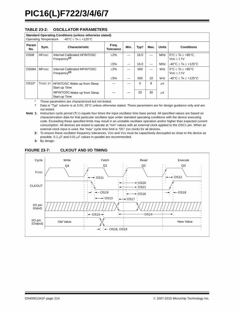
PIC16(L)F722/3/4/6/7
TABLE 23-2: OSCILLATOR PARAMETERS
FIGURE 23-7: CLKOUT AND I/O TIMING
Standard Operating Conditions (unless otherwise stated)Operating Temperature -40°C TA +125°C
Param No.
Sym. CharacteristicFreq.
ToleranceMin. Typ† Max. Units Conditions
OS08 HFOSC Internal Calibrated HFINTOSC Frequency(2)
2% — 16.0 — MHz 0°C TA +85°C, VDD V
5% — 16.0 — MHz -40°C TA +125°C
OS08A MFOSC Internal Calibrated MFINTOSC Frequency(2)
2% — 500 — kHz 0°C TA +85°CVDD V
5% — 500 10 kHz -40°C TA +125°C
OS10* TIOSC ST HFINTOSC Wake-up from Sleep Start-up Time
— — 5 8 s
MFINTOSC Wake-up from Sleep Start-up Time
— — 20 30 s
* These parameters are characterized but not tested.† Data in “Typ” column is at 3.0V, 25°C unless otherwise stated. These parameters are for design guidance only and are
not tested.Note 1: Instruction cycle period (TCY) equals four times the input oscillator time base period. All specified values are based on
characterization data for that particular oscillator type under standard operating conditions with the device executing code. Exceeding these specified limits may result in an unstable oscillator operation and/or higher than expected current consumption. All devices are tested to operate at “min” values with an external clock applied to the OSC1 pin. When an external clock input is used, the “max” cycle time limit is “DC” (no clock) for all devices.
2: To ensure these oscillator frequency tolerances, VDD and VSS must be capacitively decoupled as close to the device as possible. 0.1 F and 0.01 F values in parallel are recommended.
3: By design.
FOSC
CLKOUT
I/O pin(Input)
I/O pin(Output)
Q4 Q1 Q2 Q3
OS11
OS19
OS13
OS15
OS18, OS19
OS20OS21
OS17
OS16
OS14
OS12
OS18
Old Value New Value
Write Fetch Read ExecuteCycle
DS40001341F-page 214 2007-2015 Microchip Technology Inc.

PIC16(L)F722/3/4/6/7
TABLE 23-3: CLKOUT AND I/O TIMING PARAMETERS
FIGURE 23-8: RESET, WATCHDOG TIMER, OSCILLATOR START-UP TIMER AND POWER-UP TIMER TIMING
Standard Operating Conditions (unless otherwise stated)Operating Temperature -40°C TA +125°C
Param No.
Sym. Characteristic Min. Typ† Max. Units Conditions
OS11 TosH2ckL Fosc to CLKOUT (1) — — 70 ns VDD = 3.3-5.0V
OS12 TosH2ckH Fosc to CLKOUT (1) — — 72 ns VDD = 3.3-5.0V
OS13 TckL2ioV CLKOUT to Port out valid(1) — — 20 ns
OS14 TioV2ckH Port input valid before CLKOUT(1) TOSC + 200 ns — — ns
OS15 TosH2ioV Fosc (Q1 cycle) to Port out valid — 50 70* ns VDD = 3.3-5.0V
OS16 TosH2ioI Fosc (Q2 cycle) to Port input invalid (I/O in hold time)
50 — — ns VDD = 3.3-5.0V
OS17 TioV2osH Port input valid to Fosc(Q2 cycle)(I/O in setup time)
20 — — ns
OS18 TioR Port output rise time(2) ——
4015
7232
ns VDD = 2.0VVDD = 3.3-5.0V
OS19 TioF Port output fall time(2) ——
2815
5530
ns VDD = 2.0VVDD = 3.3-5.0V
OS20* Tinp INT pin input high or low time 25 — — ns
OS21* Trbp PORTB interrupt-on-change new input level time
TCY — — ns
* These parameters are characterized but not tested.† Data in “Typ” column is at 3.0V, 25C unless otherwise stated.
Note 1: Measurements are taken in RC mode where CLKOUT output is 4 x TOSC.2: Includes OSC2 in CLKOUT mode.
VDD
MCLR
InternalPOR
PWRTTime-out
OSCStart-Up Time
Internal Reset(1)
Watchdog Timer
33
32
30
3134
I/O pins
34
Note 1: Asserted low.
Reset(1)
2007-2015 Microchip Technology Inc. DS40001341F-page 215

PIC16(L)F722/3/4/6/7
FIGURE 23-9: BROWN-OUT RESET TIMING AND CHARACTERISTICS
VBOR
VDD
(Device in Brown-out Reset) (Device not in Brown-out Reset)
33(1)
Note 1: 64 ms delay only if PWRTE bit in the Configuration Word register is programmed to ‘0’.
Reset
(due to BOR)
VBOR and VHYST
37
DS40001341F-page 216 2007-2015 Microchip Technology Inc.

PIC16(L)F722/3/4/6/7
TABLE 23-4: RESET, WATCHDOG TIMER, OSCILLATOR START-UP TIMER, POWER-UP TIMER, AND BROWN-OUT RESET PARAMETERS
FIGURE 23-10: TIMER0 AND TIMER1 EXTERNAL CLOCK TIMINGS
Standard Operating Conditions (unless otherwise stated)Operating Temperature -40°C TA +125°C
Param No.
Sym. Characteristic Min. Typ† Max. Units Conditions
30 TMCL MCLR Pulse Width (low) 2 5
——
——
ss
VDD = 3.3-5V, -40°C to +85°CVDD = 3.3-5V
31 TWDTLP Low Power Watchdog Timer Time-out Period (No Prescaler)
10 18 27 ms VDD = 3.3V-5V
32 TOST Oscillator Start-up Timer Period(1), (2) — 1024 — Tosc (Note 3)
33* TPWRT Power-up Timer Period, PWRTE = 0 40 65 140 ms
34* TIOZ I/O high-impedance from MCLR Low or Watchdog Timer Reset
— — 2.0 s
35 VBOR Brown-out Reset Voltage 2.381.80
2.51.9
2.732.11
V BORV=2.5VBORV=1.9V
36* VHYST Brown-out Reset Hysteresis 0 25 50 mV -40°C to +85°C
37* TBORDC Brown-out Reset DC Response Time
1 3 510
s VDD VBOR, -40°C to +85°CVDD VBOR
* These parameters are characterized but not tested.† Data in “Typ” column is at 3.0V, 25°C unless otherwise stated. These parameters are for design guidance
only and are not tested.Note 1: Instruction cycle period (TCY) equals four times the input oscillator time base period. All specified values are
based on characterization data for that particular oscillator type under standard operating conditions with the device executing code. Exceeding these specified limits may result in an unstable oscillator operation and/or higher than expected current consumption. All devices are tested to operate at “min” values with an external clock applied to the OSC1 pin. When an external clock input is used, the “max” cycle time limit is “DC” (no clock) for all devices.
2: By design.3: Period of the slower clock.4: To ensure these voltage tolerances, VDD and VSS must be capacitively decoupled as close to the device as
possible. 0.1 F and 0.01 F values in parallel are recommended.
T0CKI
T1CKI
40 41
42
45 46
47 49
TMR0 orTMR1
2007-2015 Microchip Technology Inc. DS40001341F-page 217

PIC16(L)F722/3/4/6/7
TABLE 23-5: TIMER0 AND TIMER1 EXTERNAL CLOCK REQUIREMENTS
FIGURE 23-11: CAPTURE/COMPARE/PWM TIMINGS (CCP)
TABLE 23-6: CAPTURE/COMPARE/PWM REQUIREMENTS (CCP)
Standard Operating Conditions (unless otherwise stated)Operating Temperature -40°C TA +125°C
Param No.
Sym. Characteristic Min. Typ† Max. Units Conditions
40* TT0H T0CKI High Pulse Width No Prescaler 0.5 TCY + 20 — — ns
With Prescaler 10 — — ns
41* TT0L T0CKI Low Pulse Width No Prescaler 0.5 TCY + 20 — — ns
With Prescaler 10 — — ns
42* TT0P T0CKI Period Greater of:20 or TCY + 40
N
— — ns N = prescale value (2, 4, ..., 256)
45* TT1H T1CKI High Time
Synchronous, No Prescaler 0.5 TCY + 20 — — ns
Synchronous, with Prescaler 15 — — ns
Asynchronous 30 — — ns
46* TT1L T1CKI Low Time
Synchronous, No Prescaler 0.5 TCY + 20 — — ns
Synchronous, with Prescaler 15 — — ns
Asynchronous 30 — — ns
47* TT1P T1CKI Input Period
Synchronous Greater of:30 or TCY + 40
N
— — ns N = prescale value (1, 2, 4, 8)
Asynchronous 60 — — ns
48 FT1 Timer1 Oscillator Input Frequency Range (oscillator enabled by setting bit T1OSCEN)
32.4 32.768 33.1 kHz
49* TCKEZTMR1 Delay from External Clock Edge to Timer Increment
2 TOSC — 7 TOSC — Timers in Sync mode
* These parameters are characterized but not tested.† Data in “Typ” column is at 3.0V, 25°C unless otherwise stated. These parameters are for design guidance only and are not
tested.
Standard Operating Conditions (unless otherwise stated)Operating Temperature -40°C TA +125°C
Param No.
Sym. Characteristic Min. Typ† Max. Units Conditions
CC01* TccL CCPx Input Low Time No Prescaler 0.5TCY + 20 — — ns
With Prescaler 20 — — ns
CC02* TccH CCPx Input High Time No Prescaler 0.5TCY + 20 — — ns
With Prescaler 20 — — ns
CC03* TccP CCPx Input Period 3TCY + 40N
— — ns N = prescale value (1, 4 or 16)
* These parameters are characterized but not tested.† Data in “Typ” column is at 3.0V, 25°C unless otherwise stated. These parameters are for design guidance only and are not
tested.
Note: Refer to Figure 23-2 for load conditions.
(Capture mode)
CC01 CC02
CC03
CCPx
DS40001341F-page 218 2007-2015 Microchip Technology Inc.

PIC16(L)F722/3/4/6/7
TABLE 23-7: PIC16F722/3/4/6/7 A/D CONVERTER (ADC) CHARACTERISTICS:
TABLE 23-8: PIC16F722/3/4/6/7 A/D CONVERSION REQUIREMENTS
Standard Operating Conditions (unless otherwise stated)Operating temperature -40°C TA +125°C
Param No.
Sym. Characteristic Min. Typ† Max. Units Conditions
AD01 NR Resolution — — 8 bit
AD02 EIL Integral Error — — ±1.7 LSb VREF = 3.0V
AD03 EDL Differential Error — — ±1 LSb No missing codesVREF = 3.0V
AD04 EOFF Offset Error — — ±2.2 LSb VREF = 3.0V
AD05 EGN Gain Error — — ±1.5 LSb VREF = 3.0V
AD06 VREF Reference Voltage(3) 1.8 — VDD V
AD07 VAIN Full-Scale Range VSS — VREF V
AD08 ZAIN Recommended Impedance of Analog Voltage Source
— — 50 k Can go higher if external 0.01F capacitor is present on input pin.
† Data in “Typ” column is at 3.0V, 25°C unless otherwise stated. These parameters are for design guidance only and are not tested.
Note 1: Total Absolute Error includes integral, differential, offset and gain errors.2: The A/D conversion result never decreases with an increase in the input voltage and has no missing codes.3: When ADC is off, it will not consume any current other than leakage current. The power-down current specification
includes any such leakage from the ADC module.
Standard Operating Conditions (unless otherwise stated)Operating temperature -40°C TA +125°C
ParamNo.
Sym. Characteristic Min. Typ† Max. Units Conditions
AD130* TAD A/D Clock Period 1.0 — 9.0 s TOSC-based
A/D Internal RC Oscillator Period
1.0 2.0 6.0 s ADCS<1:0> = 11 (ADRC mode)
AD131 TCNV Conversion Time (not including Acquisition Time)(1)
— 10.5 — TAD Set GO/DONE bit to conversioncomplete
AD132* TACQ Acquisition Time — 1.0 — s
* These parameters are characterized but not tested.† Data in “Typ” column is at 3.0V, 25°C unless otherwise stated. These parameters are for design guidance only and are not
tested.Note 1: The ADRES register may be read on the following TCY cycle.
2007-2015 Microchip Technology Inc. DS40001341F-page 219

PIC16(L)F722/3/4/6/7
FIGURE 23-12: PIC16F722/3/4/6/7 A/D CONVERSION TIMING (NORMAL MODE)
FIGURE 23-13: PIC16F722/3/4/6/7 A/D CONVERSION TIMING (SLEEP MODE)
AD131
AD130
BSF ADCON0, GO
Q4
A/D CLK
A/D Data
ADRES
ADIF
GO
Sample
OLD_DATA
Sampling Stopped
DONE
NEW_DATA
7 6 5 3 2 1 0
Note 1: If the A/D clock source is selected as RC, a time of TCY is added before the A/D clock starts. This allows the SLEEP instruction to be executed.
1 TCY
4
AD134 (TOSC/2(1))
1 TCY
AD132
AD132
AD131
AD130
BSF ADCON0, GO
Q4
A/D CLK
A/D Data
ADRES
ADIF
GO
Sample
OLD_DATA
Sampling Stopped
DONE
NEW_DATA
7 5 3 2 1 0
Note 1: If the A/D clock source is selected as RC, a time of TCY is added before the A/D clock starts. This allows the SLEEP instruction to be executed.
AD134
46
1 TCY(TOSC/2 + TCY(1))
1 TCY
DS40001341F-page 220 2007-2015 Microchip Technology Inc.

PIC16(L)F722/3/4/6/7
FIGURE 23-14: USART SYNCHRONOUS TRANSMISSION (MASTER/SLAVE) TIMING
TABLE 23-9: USART SYNCHRONOUS TRANSMISSION REQUIREMENTS
FIGURE 23-15: USART SYNCHRONOUS RECEIVE (MASTER/SLAVE) TIMING
TABLE 23-10: USART SYNCHRONOUS RECEIVE REQUIREMENTS
Standard Operating Conditions (unless otherwise stated)Operating Temperature -40°C TA +125°C
Param. No.
Symbol Characteristic Min. Max. Units Conditions
US120 TCKH2DTV SYNC XMIT (Master and Slave)Clock high to data-out valid
3.0-5.5V — 80 ns
1.8-5.5V — 100 ns
US121 TCKRF Clock out rise time and fall time (Master mode)
3.0-5.5V — 45 ns
1.8-5.5V — 50 ns
US122 TDTRF Data-out rise time and fall time 3.0-5.5V — 45 ns
1.8-5.5V — 50 ns
Standard Operating Conditions (unless otherwise stated)Operating Temperature -40°C TA +125°C
Param. No.
Symbol Characteristic Min. Max. Units Conditions
US125 TDTV2CKL SYNC RCV (Master and Slave)Data-hold before CK (DT hold time) 10 — ns
US126 TCKL2DTL Data-hold after CK (DT hold time) 15 — ns
Note: Refer to Figure 23-2 for load conditions.
US121 US121
US120 US122
CK
DT
Note: Refer to Figure 23-2 for load conditions.
US125
US126
CK
DT
2007-2015 Microchip Technology Inc. DS40001341F-page 221

PIC16(L)F722/3/4/6/7
FIGURE 23-16: SPI MASTER MODE TIMING (CKE = 0, SMP = 0)
FIGURE 23-17: SPI MASTER MODE TIMING (CKE = 1, SMP = 1)
SS
SCK(CKP = 0)
SCK(CKP = 1)
SDO
SDI
SP70
SP71 SP72
SP73SP74
SP75, SP76
SP78SP79
SP80
SP79SP78
MSb LSbbit 6 - - - - - -1
MSb In LSb Inbit 6 - - - -1
Note: Refer to Figure 23-2 for load conditions.
SS
SCK(CKP = 0)
SCK(CKP = 1)
SDO
SDI
SP81
SP71 SP72
SP74
SP75, SP76
SP78SP80
MSb
SP79SP73
MSb In
bit 6 - - - - - -1
LSb Inbit 6 - - - -1
LSb
Note: Refer to Figure 23-2 for load conditions.
DS40001341F-page 222 2007-2015 Microchip Technology Inc.

PIC16(L)F722/3/4/6/7
FIGURE 23-18: SPI SLAVE MODE TIMING (CKE = 0)
FIGURE 23-19: SPI SLAVE MODE TIMING (CKE = 1)
SS
SCK(CKP = 0)
SCK(CKP = 1)
SDO
SDI
SP70
SP71 SP72
SP73
SP74
SP75, SP76 SP77
SP78SP79
SP80
SP79SP78
MSb LSbbit 6 - - - - - -1
MSb In bit 6 - - - -1 LSb In
SP83
Note: Refer to Figure 23-2 for load conditions.
SS
SCK(CKP = 0)
SCK(CKP = 1)
SDO
SDI
SP70
SP71 SP72
SP82
SP74
SP75, SP76
MSb bit 6 - - - - - -1 LSb
SP77
MSb In bit 6 - - - -1 LSb In
SP80
SP83
Note: Refer to Figure 23-2 for load conditions.
2007-2015 Microchip Technology Inc. DS40001341F-page 223

PIC16(L)F722/3/4/6/7
TABLE 23-11: SPI MODE REQUIREMENTS
FIGURE 23-20: I2C BUS START/STOP BITS TIMING
Param No.
Symbol Characteristic Min. Typ† Max. Units Conditions
SP70* TSSL2SCH, TSSL2SCL
SS to SCK or SCK input TCY — — ns
SP71* TSCH SCK input high time (Slave mode) TCY + 20 — — ns
SP72* TSCL SCK input low time (Slave mode) TCY + 20 — — ns
SP73* TDIV2SCH, TDIV2SCL
Setup time of SDI data input to SCK edge 100 — — ns
SP74* TSCH2DIL, TSCL2DIL
Hold time of SDI data input to SCK edge 100 — — ns
SP75* TDOR SDO data output rise time 3.0-5.5V — 10 25 ns
1.8-5.5V — 25 50 ns
SP76* TDOF SDO data output fall time — 10 25 ns
SP77* TSSH2DOZ SS to SDO output high-impedance 10 — 50 ns
SP78* TSCR SCK output rise time (Master mode)
3.0-5.5V — 10 25 ns
1.8-5.5V — 25 50 ns
SP79* TSCF SCK output fall time (Master mode) — 10 25 ns
SP80* TSCH2DOV,TSCL2DOV
SDO data output valid after SCK edge
3.0-5.5V — — 50 ns
1.8-5.5V — — 145 ns
SP81* TDOV2SCH,TDOV2SCL
SDO data output setup to SCK edge Tcy — — ns
SP82* TSSL2DOV SDO data output valid after SS edge — — 50 ns
SP83* TSCH2SSH,TSCL2SSH
SS after SCK edge 1.5TCY + 40 — — ns
* These parameters are characterized but not tested.† Data in “Typ” column is at 3.0V, 25°C unless otherwise stated. These parameters are for design guidance
only and are not tested.
Note: Refer to Figure 23-2 for load conditions.
SP91
SP92
SP93SCL
SDA
StartCondition
StopCondition
SP90
DS40001341F-page 224 2007-2015 Microchip Technology Inc.

PIC16(L)F722/3/4/6/7
TABLE 23-12: I2C BUS START/STOP BITS REQUIREMENTS
FIGURE 23-21: I2C BUS DATA TIMING
ParamNo.
Symbol Characteristic Min. Typ Max. Units Conditions
SP90* TSU:STA Start condition 100 kHz mode 4700 — — ns Only relevant for Repeated Start conditionSetup time 400 kHz mode 600 — —
SP91* THD:STA Start condition 100 kHz mode 4000 — — ns After this period, the first clock pulse is generatedHold time 400 kHz mode 600 — —
SP92* TSU:STO Stop condition 100 kHz mode 4700 — — ns
Setup time 400 kHz mode 600 — —
SP93 THD:STO Stop condition 100 kHz mode 4000 — — ns
Hold time 400 kHz mode 600 — —
* These parameters are characterized but not tested.
Note: Refer to Figure 23-2 for load conditions.
SP90
SP91 SP92
SP100SP101
SP103
SP106SP107
SP109SP109
SP110
SP102
SCL
SDAIn
SDAOut
2007-2015 Microchip Technology Inc. DS40001341F-page 225

PIC16(L)F722/3/4/6/7
TABLE 23-13: I2C BUS DATA REQUIREMENTS
Param.No.
Symbol Characteristic Min. Max. Units Conditions
SP100* THIGH Clock high time 100 kHz mode 4.0 — s Device must operate at a minimum of 1.5 MHz
400 kHz mode 0.6 — s Device must operate at a minimum of 10 MHz
SSP Module 1.5TCY —
SP101* TLOW Clock low time 100 kHz mode 4.7 — s Device must operate at a minimum of 1.5 MHz
400 kHz mode 1.3 — s Device must operate at a minimum of 10 MHz
SSP Module 1.5TCY —
SP102* TR SDA and SCL rise time
100 kHz mode — 1000 ns
400 kHz mode 20 + 0.1CB 300 ns CB is specified to be from 10-400 pF
SP103* TF SDA and SCL fall time 100 kHz mode — 250 ns
400 kHz mode 20 + 0.1CB 250 ns CB is specified to be from 10-400 pF
SP106* THD:DAT Data input hold time 100 kHz mode 0 — ns
400 kHz mode 0 0.9 s
SP107* TSU:DAT Data input setup time 100 kHz mode 250 — ns (Note 2)
400 kHz mode 100 — ns
SP109* TAA Output valid from clock
100 kHz mode — 3500 ns (Note 1)
400 kHz mode — — ns
SP110* TBUF Bus free time 100 kHz mode 4.7 — s Time the bus must be free before a new transmission can start
400 kHz mode 1.3 — s
SP111 CB Bus capacitive loading — 400 pF
* These parameters are characterized but not tested.Note 1: As a transmitter, the device must provide this internal minimum delay time to bridge the undefined region (min. 300 ns)
of the falling edge of SCL to avoid unintended generation of Start or Stop conditions.2: A Fast mode (400 kHz) I2C bus device can be used in a Standard mode (100 kHz) I2C bus system, but the requirement
TSU:DAT 250 ns must then be met. This will automatically be the case if the device does not stretch the low period of the SCL signal. If such a device does stretch the low period of the SCL signal, it must output the next data bit to the SDA line TR max. + TSU:DAT = 1000 + 250 = 1250 ns (according to the Standard mode I2C bus specification), before the SCL line is released.
DS40001341F-page 226 2007-2015 Microchip Technology Inc.

PIC16(L)F722/3/4/6/7
TABLE 23-14: CAP SENSE OSCILLATOR SPECIFICATIONS
FIGURE 23-22: CAP SENSE OSCILLATOR
Param.No.
Symbol Characteristic Min. Typ† Max. Units Conditions
CS01 ISRC Current Source High — -5.8 -6 A-40, -85°CMedium — -1.1 -3.2 A
Low — -0.2 -0.9 A
CS02 ISNK Current Sink High — 6.6 6 A-40, -85°CMedium — 1.3 3.2 A
Low — 0.24 0.9 A
CS03 VCHYST Cap Hysteresis High — 525 — mVVCTH-VCTLMedium — 375 — mV
Low — 280 — mV
* These parameters are characterized but not tested.
† Data in “Typ” column is at 3.0V, 25°C unless otherwise stated. These parameters are for design guidance only and are not tested.
ISRC
VCTH
VCTL
ISNKEnabledEnabled
2007-2015 Microchip Technology Inc. DS40001341F-page 227

PIC16(L)F722/3/4/6/7
24.0 DC AND AC CHARACTERISTICS GRAPHS AND CHARTS
FIGURE 24-1: PIC16F722/3/4/6/7 MAXIMUM IDD vs. FOSC OVER VDD, EC MODE, VCAP = 0.1 µF
FIGURE 24-2: PIC16LF722/3/4/6/7 MAXIMUM IDD vs. FOSC OVER VDD, EC MODE
1.8V
2.5V
3V
3.6V
5V
0.00
200.00
400.00
600.00
800.00
1,000.00
1,200.00
1,400.00
1,600.00
1,800.00
2,000.00
2,200.00
1 MHz 4 MHz 8 MHz 12 MHz 16 MHz 20 MHz
VDD (V)
Typical: Statistical Mean @25°C
Maximum: Mean (Worst-Case Temp) + 3(-40°C to 125°C)
IDD
(µ
A)
1.8V
2V
2.5V
3V
3.3V
3.6V
0
200
400
600
800
1,000
1,200
1,400
1,600
1,800
2,000
2,200
2,400
1 MHz 4 MHz 8 MHz 12 MHz 16 MHz 20 MHz
Typical: Statistical Mean @25°C
Maximum: Mean (Worst-Case Temp) + 3(-40°C to 125°C)
FOSC
IDD
(µ
A)
DS40001341F-page 228 2007-2015 Microchip Technology Inc.

PIC16(L)F722/3/4/6/7
FIGURE 24-3: PIC16F722/3/4/6/7 TYPICAL IDD vs. FOSC OVER VDD, EC MODE, VCAP = 0.1 µF
FIGURE 24-4: PIC16LF722/3/4/6/7 TYPICAL IDD vs. FOSC OVER VDD, EC MODE
1.8V
2.5V
3V
3.6V
5V
0
200
400
600
800
1,000
1,200
1,400
1,600
1,800
2,000
1 MHz 4 MHz 8 MHz 12 MHz 16 MHz 20 MHz
Typical: Statistical Mean @25°C
Maximum: Mean (Worst-Case Temp) + 3(-40°C to 125°C)
FOSC
IDD
(µ
A)
1.8V
2V
2.5V
3V
3.3V
3.6V
0
200
400
600
800
1,000
1,200
1,400
1,600
1,800
2,000
2,200
1 MHz 4 MHz 8 MHz 12 MHz 16 MHz 20 MHz
Typical: Statistical Mean @25°C
Maximum: Mean (Worst-Case Temp) + 3(-40°C to 125°C)
IDD
(µ
A)
FOSC
2007-2015 Microchip Technology Inc. DS40001341F-page 229

PIC16(L)F722/3/4/6/7
FIGURE 24-5: PIC16F722/3/4/6/7 MAXIMUM IDD vs. VDD OVER FOSC, EXTRC MODE, VCAP = 0.1 µF
FIGURE 24-6: PIC16LF722/3/4/6/7 MAXIMUM IDD vs. VDD OVER FOSC, EXTRC MODE
1 MHz
4 MHz
0
100
200
300
400
500
600
1.8 2 2.5 3 3.3 3.6 4.2 4.5 5
Typical: Statistical Mean @25°C
Maximum: Mean (Worst-Case Temp) + 3(-40°C to 125°C)
IDD
(µ
A)
VDD (V)
1 MHz
4 MHz
0
50
100
150
200
250
300
350
400
450
500
1.8 2 2.5 3 3.3 3.6
Typical: Statistical Mean @25°C
Maximum: Mean (Worst-Case Temp) + 3(-40°C to 125°C)
IDD
(µ
A)
VDD (V)
DS40001341F-page 230 2007-2015 Microchip Technology Inc.

PIC16(L)F722/3/4/6/7
FIGURE 24-7: PIC16F722/3/4/6/7 TYPICAL IDD vs. VDD OVER FOSC, EXTRC MODE, VCAP = 0.1 µF
FIGURE 24-8: PIC16LF722/3/4/6/7 TYPICAL IDD vs. VDD OVER FOSC, EXTRC MODE
1 MHz
4 MHz
0
50
100
150
200
250
300
350
400
450
1.8 2 2.5 3 3.3 3.6 4.2 4.5 5
Typical: Statistical Mean @25°C
Maximum: Mean (Worst-Case Temp) + 3(-40°C to 125°C)
VDD (V)
IDD
(µ
A)
1 MHz
4 MHz
0
50
100
150
200
250
300
350
400
450
1.8 2 2.5 3 3.3 3.6
Typical: Statistical Mean @25°C
Maximum: Mean (Worst-Case Temp) + 3(-40°C to 125°C)
VDD (V)
IDD
(µ
A)
2007-2015 Microchip Technology Inc. DS40001341F-page 231

PIC16(L)F722/3/4/6/7
FIGURE 24-9: PIC16F722/3/4/6/7 MAXIMUM IDD vs. FOSC OVER VDD, HS MODE, VCAP = 0.1 µF
FIGURE 24-10: PIC16LF722/3/4/6/7 MAXIMUM IDD vs. FOSC OVER VDD, HS MODE
3V
3.6V
4.5V
0
0.2
0.4
0.6
0.8
1
1.2
1.4
1.6
1.8
2
2.2
2.4
4 MHz 6 MHz 8 MHz 10 MHz 13 MHz 16 MHz 20 MHz
Typical: Statistical Mean @25°C
Maximum: Mean (Worst-Case Temp) + 3(-40°C to 125°C)
Fosc
IDD
(m
A)
5V
2.5V
3V
3.6V
0.00
0.50
1.00
1.50
2.00
2.50
4 MHz 6 MHz 8 MHz 10 MHz 13 MHz 16 MHz 20 MHz
Typical: Statistical Mean @25°C
Maximum: Mean (Worst-Case Temp) + 3(-40°C to 125°C)
Fosc
IDD
(m
A)
3.3V
DS40001341F-page 232 2007-2015 Microchip Technology Inc.

PIC16(L)F722/3/4/6/7
FIGURE 24-11: PIC16F722/3/4/6/7 TYPICAL IDD vs. FOSC OVER VDD, HS MODE, VCAP = 0.1 µF
FIGURE 24-12: PIC16LF722/3/4/6/7 TYPICAL IDD vs. FOSC OVER VDD, HS MODE
3V
3.6V
4.5V
0.00
0.50
1.00
1.50
2.00
4 MHz 6 MHz 8 MHz 10 MHz 13 MHz 16 MHz 20 MHz
Typical: Statistical Mean @25°C
Maximum: Mean (Worst-Case Temp) + 3(-40°C to 125°C)
Fosc
IDD
(m
A)
5V
2.5V
3V
3.3V
0.00
0.50
1.00
1.50
2.00
2.50
4 MHz 6 MHz 8 MHz 10 MHz 13 MHz 16 MHz 20 MHz
Typical: Statistical Mean @25°C
Maximum: Mean (Worst-Case Temp) + 3(-40°C to 125°C)
IDD
(m
A)
Fosc
3.6V
2007-2015 Microchip Technology Inc. DS40001341F-page 233

PIC16(L)F722/3/4/6/7
FIGURE 24-13: PIC16F722/3/4/6/7 MAXIMUM IDD vs. VDD OVER FOSC, XT MODE, VCAP = 0.1 µF
FIGURE 24-14: PIC16LF722/3/4/6/7 MAXIMUM IDD vs. VDD OVER FOSC, XT MODE
1 MHz
4 MHz
0
100
200
300
400
500
600
1.8 2 2.5 3 3.3 3.6 4.2 4.5 5
Typical: Statistical Mean @25°C
Maximum: Mean (Worst-Case Temp) + 3(-40°C to 125°C)
IDD
(µ
A)
VDD (V)
1 MHz
4 MHz
0
100
200
300
400
500
600
1.8 2 2.5 3 3.3 3.6
IDD
(µ
A)
Typical: Statistical Mean @25°C
Maximum: Mean (Worst-Case Temp) + 3(-40°C to 125°C)
VDD (V)
DS40001341F-page 234 2007-2015 Microchip Technology Inc.

PIC16(L)F722/3/4/6/7
FIGURE 24-15: PIC16F722/3/4/6/7 TYPICAL IDD vs. VDD OVER FOSC, XT MODE, VCAP = 0.1 µF
FIGURE 24-16: PIC16LF722/3/4/6/7 TYPICAL IDD vs. VDD OVER FOSC, XT MODE
1 MHz
4 MHz
0
100
200
300
400
500
600
1.8 2 2.5 3 3.3 3.6 4.2 4.5 5
Typical: Statistical Mean @25°C
Maximum: Mean (Worst-Case Temp) + 3(-40°C to 125°C)
IDD
(µ
A)
VDD (V)
1 MHz
4 MHz
0
100
200
300
400
500
600
1.8 2 2.5 3 3.3 3.6
Typical: Statistical Mean @25°C
Maximum: Mean (Worst-Case Temp) + 3(-40°C to 125°C)
IDD
(µ
A)
VDD (V)
2007-2015 Microchip Technology Inc. DS40001341F-page 235

PIC16(L)F722/3/4/6/7
FIGURE 24-17: PIC16F722/3/4/6/7 IDD vs. VDD, LP MODE, VCAP = 0.1 µF
FIGURE 24-18: PIC16LF722/3/4/6/7 IDD vs. VDD, LP MODE
32 kHz Typical
32 kHz Maximum
10.0
12.5
15.0
17.5
20.0
1.8 3 5
Typical: Statistical Mean @25°C
Maximum: Mean (Worst-Case Temp) + 3(-40°C to 125°C)
IDD
(µ
A)
VDD (V)
VDD (V)
32 kHz Typical
32 kHz Maximum
5
10
15
20
25
30
1.8 3 3.3 3.6
Typical: Statistical Mean @25°C
Maximum: Mean (Worst-Case Temp) + 3(-40°C to 125°C)
IDD
(µ
A)
VDD (V)
DS40001341F-page 236 2007-2015 Microchip Technology Inc.

PIC16(L)F722/3/4/6/7
FIGURE 24-19: PIC16F722/3/4/6/7 MAXIMUM IDD vs. FOSC OVER VDD, INTOSC MODE, VCAP = 0.1 µF
FIGURE 24-20: PIC16LF722/3/4/6/7 MAXIMUM IDD vs. FOSC OVER VDD, INTOSC MODE
110
120
130
140
150
160
170
180
190
200
210
62.5 kHz 125 kHz 250 kHz 500 kHz
5V
3.6V
1.8V
2.5V
Typical: Statistical Mean @25°C
Maximum: Mean (Worst-Case Temp) + 3(-40°C to 125°C)
FOSC
IDD
(µ
A)
1.8V
2.5V
3V
3.6V
100
110
120
130
140
150
160
170
62.5 KHz 125 KHz 250 KHz 500 KHz
Typical: Statistical Mean @25°C
Maximum: Mean (Worst-Case Temp) + 3(-40°C to 125°C)
FOSC
IDD
(µ
A)
2007-2015 Microchip Technology Inc. DS40001341F-page 237
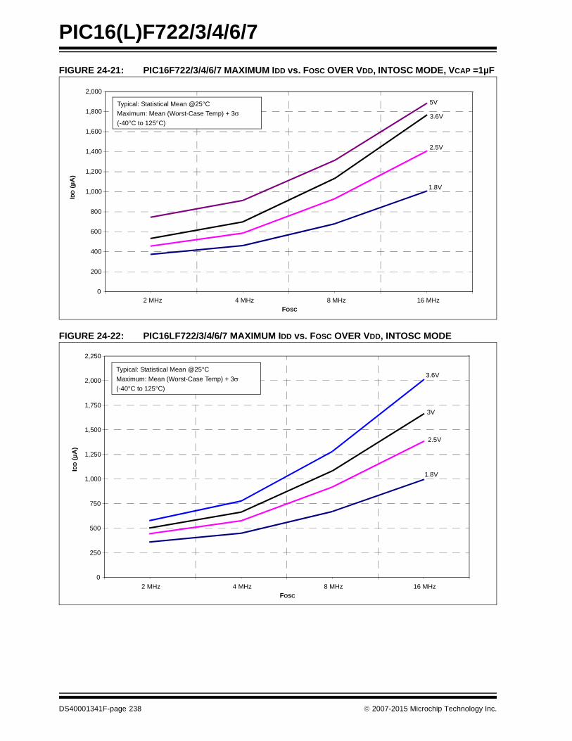
PIC16(L)F722/3/4/6/7
FIGURE 24-21: PIC16F722/3/4/6/7 MAXIMUM IDD vs. FOSC OVER VDD, INTOSC MODE, VCAP =1µF
FIGURE 24-22: PIC16LF722/3/4/6/7 MAXIMUM IDD vs. FOSC OVER VDD, INTOSC MODE
0
200
400
600
800
1,000
1,200
1,400
1,600
1,800
2,000
2 MHz 4 MHz 8 MHz 16 MHz
Typical: Statistical Mean @25°C
Maximum: Mean (Worst-Case Temp) + 3(-40°C to 125°C)
IDD
(µ
A)
FOSC
1.8V
2.5V
5V
3.6V
1.8V
2.5V
3V
3.6V
0
250
500
750
1,000
1,250
1,500
1,750
2,000
2,250
2 MHz 4 MHz 8 MHz 16 MHz
sTypical: Statistical Mean @25°C
Maximum: Mean (Worst-Case Temp) + 3(-40°C to 125°C)
IDD
(µ
A)
FOSC
DS40001341F-page 238 2007-2015 Microchip Technology Inc.

PIC16(L)F722/3/4/6/7
FIGURE 24-23: PIC16F722/3/4/6/7 TYPICAL IDD vs. FOSC OVER VDD, INTOSC MODE, VCAP =0.1µF
FIGURE 24-24: PIC16LF722/3/4/6/7 TYPICAL IDD vs. FOSC OVER VDD, INTOSC MODE
1.8V
2.5V
3.6V
5V
80
90
100
110
120
130
140
150
160
62.5 kHz 125 kHz 250 kHz 500 kHz
Typical: Statistical Mean @25°C
Maximum: Mean (Worst-Case Temp) + 3(-40°C to 125°C)
IDD
(µ
A)
FOSC
3.6V
1.8V
2.5V
3V
70
80
90
100
110
120
130
140
62.5 kHz 125 kHz 250 kHz 500 kHz
Typical: Statistical Mean @25°C
Maximum: Mean (Worst-Case Temp) + 3(-40°C to 125°C)
IDD
(µ
A)
FOSC
2007-2015 Microchip Technology Inc. DS40001341F-page 239

PIC16(L)F722/3/4/6/7
FIGURE 24-25: PIC16F722/3/4/6/7 TYPICAL IDD vs. FOSC OVER VDD, INTOSC MODE, VCAP = 0.1 µF
FIGURE 24-26: PIC16LF722/3/4/6/7 TYPICAL IDD vs. FOSC OVER VDD, INTOSC MODE
1.8V
2.5V
3.6V
5V
0
200
400
600
800
1,000
1,200
1,400
1,600
1,800
2,000
2 MHz 4 MHz 8 MHz 16 MHz
Typical: Statistical Mean @25°C
Maximum: Mean (Worst-Case Temp) + 3(-40°C to 125°C)
IDD
(µ
A)
FOSC
3.6V
1.8V
2.5V
3V
0
200
400
600
800
1,000
1,200
1,400
1,600
1,800
2,000
2 MHz 4 MHz 8 MHz 16 MHz
Typical: Statistical Mean @25°C
Maximum: Mean (Worst-Case Temp) + 3(-40°C to 125°C)
IDD
(µ
A)
VDD (V)
DS40001341F-page 240 2007-2015 Microchip Technology Inc.

PIC16(L)F722/3/4/6/7
FIGURE 24-27: PIC16F722/3/4/6/7 MAXIMUM BASE IPD vs. VDD, VCAP = 0.1 µF
FIGURE 24-28: PIC16LF722/3/4/6/7 MAXIMUM BASE IPD vs. VDD
85°C
125°C
0
5
10
15
20
25
1.8V 2V 3V 3.6V 4V 5V 5.5V
Typical: Statistical Mean @25°C
Maximum: Mean (Worst-Case Temp) + 3(-40°C to 125°C)
IPD
(µ
A)
VDD (V)
125°C
85°C
0
1
2
3
4
5
6
7
1.8V 2V 2.5V 3V 3.6V
Typical: Statistical Mean @25°C
Maximum: Mean (Worst-Case Temp) + 3(-40°C to 125°C)
IPD
(µ
A)
VDD (V)
2007-2015 Microchip Technology Inc. DS40001341F-page 241

PIC16(L)F722/3/4/6/7
FIGURE 24-29: PIC16F722/3/4/6/7 TYPICAL BASE IPD vs. VDD, VCAP = 0.1 µF
FIGURE 24-30: PIC16LF722/3/4/6/7 TYPICAL BASE IPD vs. VDD
25°C
2
3
4
5
6
7
8
1.8V 2V 3V 3.6V 4V 5V 5.5V
Typical: Statistical Mean @25°C
Maximum: Mean (Worst-Case Temp) + 3(-40°C to 125°C)
IPD
(µ
A)
VDD (V)
25°C
0
50
100
150
200
250
1.8V 2V 2.5V 3V 3.6V
Typical: Statistical Mean @25°C
Maximum: Mean (Worst-Case Temp) + 3(-40°C to 125°C)
IPD
(n
A)
VDD (V)
DS40001341F-page 242 2007-2015 Microchip Technology Inc.

PIC16(L)F722/3/4/6/7
FIGURE 24-31: PIC16F722/3/4/6/7 FIXED VOLTAGE REFERENCE IPD vs. VDD, VCAP = 0.1 µF
FIGURE 24-32: PIC16LF722/3/4/6/7 FIXED VOLTAGE REFERENCE IPD vs. VDD
Typ. 25°C
Max. 125°C
Max. 85°C
0
10
20
30
40
50
60
70
1.8V 2V 3V 3.6V 5V 5.5V
Typical: Statistical Mean @25°C
Maximum: Mean (Worst-Case Temp) + 3(-40°C to 125°C)
IPD
(µ
A)
VDD (V)
Typ. 25°C
Max. 125°C
Max. 85°C
0
5
10
15
20
25
1.8V 2V 2.5V 3V 3.6V
Typical: Statistical Mean @25°C
Maximum: Mean (Worst-Case Temp) + 3(-40°C to 125°C)
IPD
(µ
A)
VDD (V)
2007-2015 Microchip Technology Inc. DS40001341F-page 243

PIC16(L)F722/3/4/6/7
FIGURE 24-33: PIC16F722/3/4/6/7 BOR IPD vs. VDD, VCAP = 0.1 µF
FIGURE 24-34: PIC16LF722/3/4/6/7 BOR IPD vs. VDD
Typ. 25°C
Max. 125°C
Max. 85°C
0
10
20
30
40
50
60
70
2V 3V 3.6V 5V 5.5V
Typical: Statistical Mean @25°C
Maximum: Mean (Worst-Case Temp) + 3(-40°C to 125°C)
IPD
(µ
A)
VDD (V)
Typ. 25°C
Max. 125°C
Max. 85°C
0
5
10
15
20
25
30
2V 2.5V 3V 3.6V
Typical: Statistical Mean @25°C
Maximum: Mean (Worst-Case Temp) + 3(-40°C to 125°C)
IPD
(µ
A)
VDD (V)
DS40001341F-page 244 2007-2015 Microchip Technology Inc.

PIC16(L)F722/3/4/6/7
FIGURE 24-35: PIC16F722/3/4/6/7 CAP SENSE HIGH POWER IPD vs. VDD, VCAP = 0.1 µF
FIGURE 24-36: PIC16LF722/3/4/6/7 CAP SENSE HIGH POWER IPD vs. VDD
Typ. 25°C
Max. 125°C
Max. 85°C
0
10
20
30
40
50
60
70
1.8V 2V 3V 3.6V 5V 5.5V
Typical: Statistical Mean @25°C
Maximum: Mean (Worst-Case Temp) + 3(-40°C to 125°C)
IPD
(µ
A)
VDD (V)
Typ. 25°C
Max. 125°C
Max. 85°C
0
10
20
30
40
50
60
1.8V 2V 2.5V 3V 3.6V
Typical: Statistical Mean @25°C
Maximum: Mean (Worst-Case Temp) + 3(-40°C to 125°C)
IPD
(µ
A)
VDD (V)
2007-2015 Microchip Technology Inc. DS40001341F-page 245

PIC16(L)F722/3/4/6/7
FIGURE 24-37: PIC16F722/3/4/6/7 CAP SENSE MEDIUM POWER IPD vs. VDD, VCAP = 0.1 µF
FIGURE 24-38: PIC16LF722/3/4/6/7 CAP SENSE MEDIUM POWER IPD vs. VDD
Typ. 25°C
Max. 125°C
Max. 85°C
0
5
10
15
20
25
30
1.8V 2V 3V 3.6V 5V 5.5V
Typical: Statistical Mean @25°C
Maximum: Mean (Worst-Case Temp) + 3(-40°C to 125°C)
IPD
(µ
A)
VDD (V)
Typ. 25°C
Max. 125°C
Max. 85°C
0
2
4
6
8
10
12
14
16
18
20
1.8V 2V 2.5V 3V 3.6V
Typical: Statistical Mean @25°C
Maximum: Mean (Worst-Case Temp) + 3(-40°C to 125°C)
IPD
(µ
A)
VDD (V)
DS40001341F-page 246 2007-2015 Microchip Technology Inc.

PIC16(L)F722/3/4/6/7
FIGURE 24-39: PIC16F722/3/4/6/7 CAP SENSE LOW POWER IPD vs. VDD, VCAP = 0.1 µF
FIGURE 24-40: PIC16LF722/3/4/6/7 CAP SENSE LOW POWER IPD vs. VDD
Typ. 25°C
Max. 125°C
Max. 85°C
0
5
10
15
20
25
30
1.8V 2V 3V 3.6V 5V 5.5V
Typical: Statistical Mean @25°C
Maximum: Mean (Worst-Case Temp) + 3(-40°C to 125°C)
IPD
(µ
A)
VDD (V)
Typ. 25°C
Max. 125°C
Max. 85°C
0
2
4
6
8
10
12
14
16
18
1.8V 2V 2.5V 3V 3.6V
Typical: Statistical Mean @25°C
Maximum: Mean (Worst-Case Temp) + 3(-40°C to 125°C)
IPD
(µ
A)
VDD (V)
2007-2015 Microchip Technology Inc. DS40001341F-page 247

PIC16(L)F722/3/4/6/7
FIGURE 24-41: PIC16F722/3/4/6/7 T1OSC 32 KHZ IPD vs. VDD, VCAP = 0.1 µF
FIGURE 24-42: PIC16LF722/3/4/6/7 T1OSC 32 kHz IPD vs. VDD
Typ. 25° C
Max. 85°C
0
2
4
6
8
10
12
14
16
1.8V 2V 3V 3.6V 5V 5.5V
Typical: Statistical Mean @25°C
Maximum: Mean (Worst-Case Temp) + 3(-40°C to 125°C)
IPD
(µ
A)
VDD (V)
Typ.
Max. 85°C
0.0
0.5
1.0
1.5
2.0
2.5
3.0
3.5
4.0
1.8V 2V 2.5V 3V 3.6V
Typical: Statistical Mean @25°C
Maximum: Mean (Worst-Case Temp) + 3(-40°C to 125°C)
IPD
(µ
A)
VDD (V)
DS40001341F-page 248 2007-2015 Microchip Technology Inc.
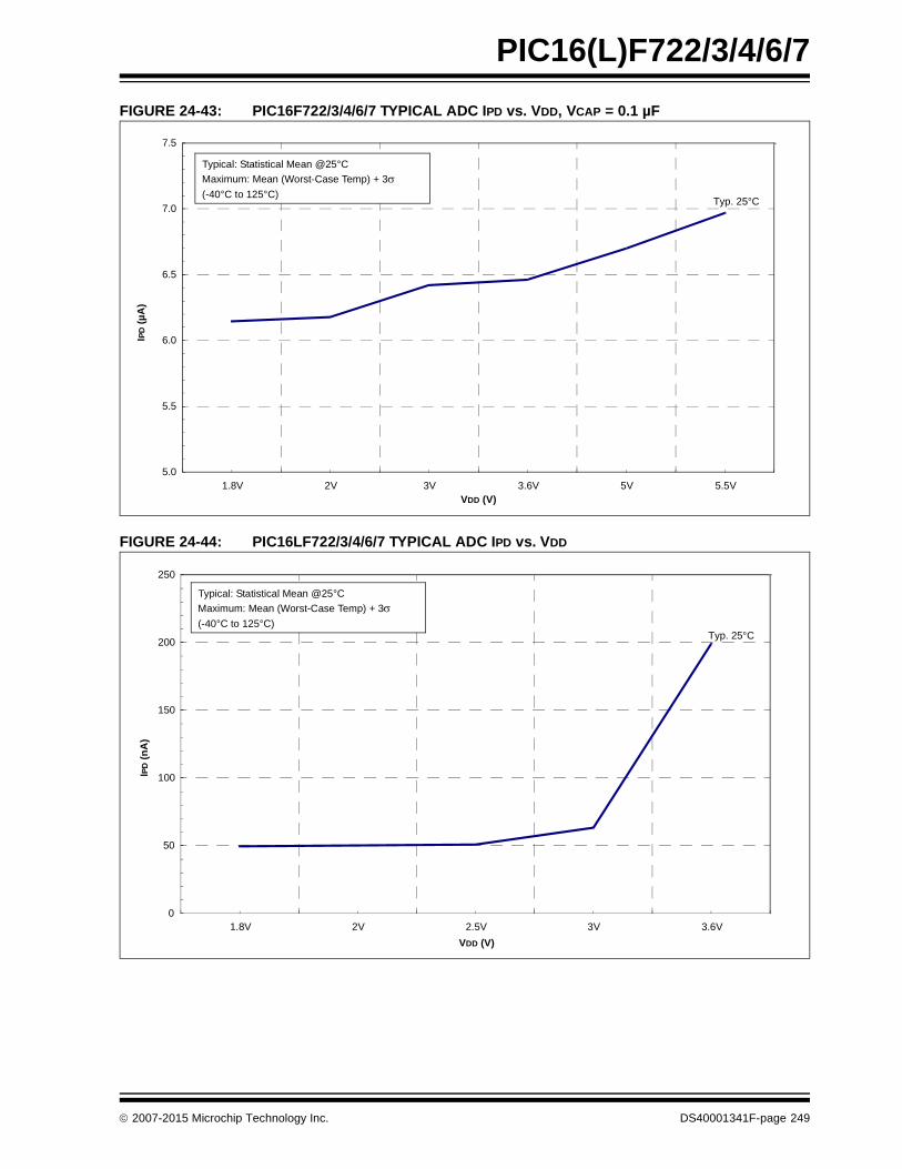
PIC16(L)F722/3/4/6/7
FIGURE 24-43: PIC16F722/3/4/6/7 TYPICAL ADC IPD vs. VDD, VCAP = 0.1 µF
FIGURE 24-44: PIC16LF722/3/4/6/7 TYPICAL ADC IPD vs. VDD
Typ. 25°C
5.0
5.5
6.0
6.5
7.0
7.5
1.8V 2V 3V 3.6V 5V 5.5V
Typical: Statistical Mean @25°C
Maximum: Mean (Worst-Case Temp) + 3(-40°C to 125°C)
IPD
(µ
A)
VDD (V)
Typ. 25°C
0
50
100
150
200
250
1.8V 2V 2.5V 3V 3.6V
Typical: Statistical Mean @25°C
Maximum: Mean (Worst-Case Temp) + 3(-40°C to 125°C)
IPD
(n
A)
VDD (V)
2007-2015 Microchip Technology Inc. DS40001341F-page 249

PIC16(L)F722/3/4/6/7
FIGURE 24-45: PIC16F722/3/4/6/7 ADC IPD vs. VDD, VCAP = 0.1 µF
FIGURE 24-46: PIC16LF722/3/4/6/7 ADC IPD vs. VDD
Max. 85°C
Max. 125°C
5
10
15
20
25
1.8V 2V 3V 3.6V 5V 5.5V
Typical: Statistical Mean @25°C
Maximum: Mean (Worst-Case Temp) + 3(-40°C to 125°C)
IPD
(µ
A)
VDD (V)
Max. 85°C
Max. 125°C
0
1
2
3
4
5
6
7
8
1.8V 2V 2.5V 3V 3.6V
Typical: Statistical Mean @25°C
Maximum: Mean (Worst-Case Temp) + 3(-40°C to 125°C)
IPD
(µ
A)
VDD (V)
DS40001341F-page 250 2007-2015 Microchip Technology Inc.

PIC16(L)F722/3/4/6/7
FIGURE 24-47: PIC16F722/3/4/6/7 WDT IPD vs. VDD, VCAP = 0.1 µF
FIGURE 24-48: PIC16LF722/3/4/6/7 WDT IPD vs. VDD
Typ. 25°C
Max. 85°C
0
2
4
6
8
10
12
14
16
18
1.8V 2V 3V 3.6V 5V 5.5V
Typical: Statistical Mean @25°C
Maximum: Mean (Worst-Case Temp) + 3(-40°C to 125°C)
IPD
(µ
A)
VDD (V)
Typ. 25°C
Max. 85°C
0.0
0.5
1.0
1.5
2.0
2.5
3.0
3.5
1.8V 2V 2.5V 3V 3.6V
Typical: Statistical Mean @25°C
Maximum: Mean (Worst-Case Temp) + 3(-40°C to 125°C)
IPD
(µ
A)
VDD (V)
2007-2015 Microchip Technology Inc. DS40001341F-page 251

PIC16(L)F722/3/4/6/7
FIGURE 24-49: TTL INPUT THRESHOLD VIN vs. VDD OVER TEMPERATURE
FIGURE 24-50: SCHMITT TRIGGER INPUT THRESHOLD VIN vs. VDD OVER TEMPERATURE
Max. -40°
Typ. 25°
Min. 125°
0.4
0.6
0.8
1
1.2
1.4
1.6
1.8
1.8 3.6 5.5
Maximum: Mean + 3 (-40°C to 125°C)
Minimum: Mean - 3 (-40°C to 125°C)
VIN
(V
)
VDD (V)
Typical: Mean @25°C
VIHMin. 125°C
0.0
0.5
1.0
1.5
2.0
2.5
3.0
3.5
1.8 3.6 5.5
VIN
(V
)
VDD (V)
VIHMax. -40°C
Maximum: Mean + 3 (-40°C to 125°C)
Minimum: Mean - 3 (-40°C to 125°C) Typical: Mean @25°C
DS40001341F-page 252 2007-2015 Microchip Technology Inc.
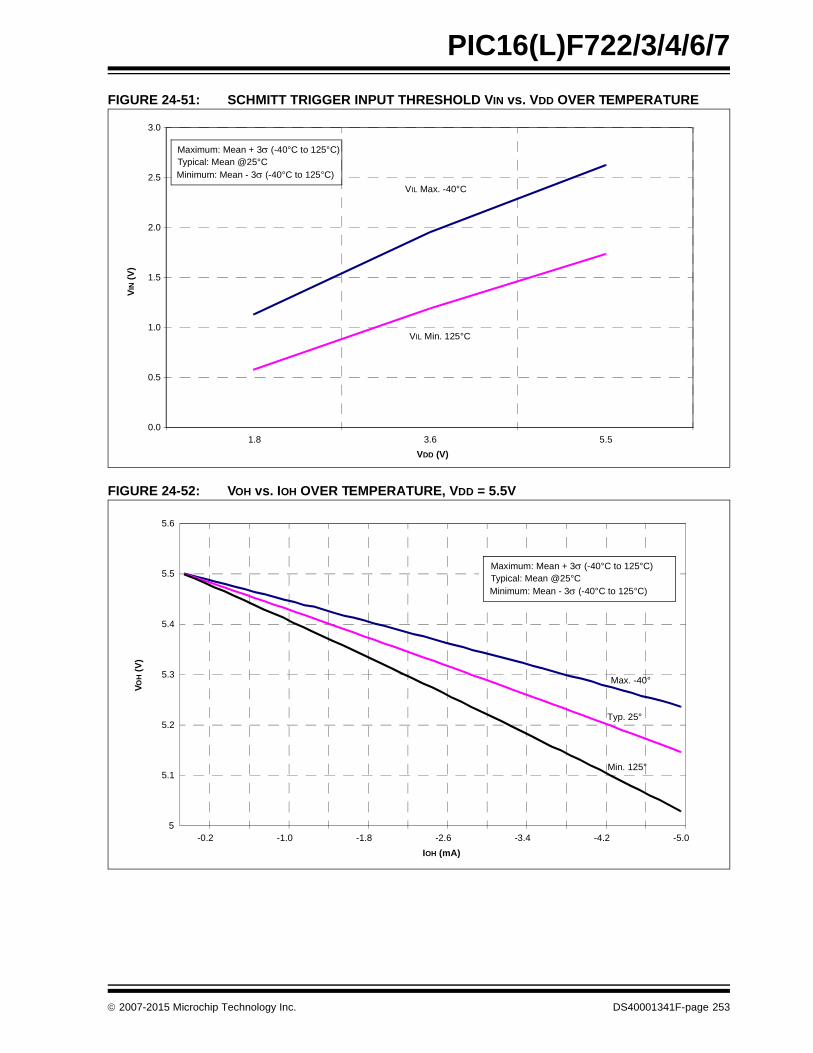
PIC16(L)F722/3/4/6/7
FIGURE 24-51: SCHMITT TRIGGER INPUT THRESHOLD VIN vs. VDD OVER TEMPERATURE
FIGURE 24-52: VOH vs. IOH OVER TEMPERATURE, VDD = 5.5V
0.0
0.5
1.0
1.5
2.0
2.5
3.0
1.8 3.6 5.5
VIN
(V
)
VDD (V)
VIL Min. 125°C
VIL Max. -40°C
Maximum: Mean + 3 (-40°C to 125°C)
Minimum: Mean - 3 (-40°C to 125°C) Typical: Mean @25°C
Max. -40°
Min. 125°
Typ. 25°
5
5.1
5.2
5.3
5.4
5.5
5.6
-5.0-4.2-3.4-2.6-1.8-1.0-0.2
Maximum: Mean + 3 (-40°C to 125°C)
Minimum: Mean - 3 (-40°C to 125°C) Typical: Mean @25°C
VO
H (
V)
IOH (mA)
2007-2015 Microchip Technology Inc. DS40001341F-page 253

PIC16(L)F722/3/4/6/7
FIGURE 24-53: VOH vs. IOH OVER TEMPERATURE, VDD = 3.6V
FIGURE 24-54: VOH vs. IOH OVER TEMPERATURE, VDD = 1.8V
2.6
2.8
3
3.2
3.4
3.6
3.8
-5.0-4.2-3.4-2.6-1.8-1.0-0.2
Maximum: Mean + 3 (-40°C to 125°C)
Minimum: Mean - 3 (-40°C to 125°C) Typical: Mean @25°C
VO
H (
V)
IOH (mA)
Max. -40°
Typ. 25°
Min. 125°
0
0.2
0.4
0.6
0.8
1
1.2
1.4
1.6
1.8
2
-2.0-1.8-1.6-1.4-1.2-1.0-0.8-0.6-0.4-0.20.0
VO
H (
V)
IOH (mA)
Max. -40°
Typ. 25°
Min. 125°
Maximum: Mean + 3 (-40°C to 125°C)
Minimum: Mean - 3 (-40°C to 125°C) Typical: Mean @25°C
DS40001341F-page 254 2007-2015 Microchip Technology Inc.

PIC16(L)F722/3/4/6/7
FIGURE 24-55: VOL vs. IOL OVER TEMPERATURE, VDD = 5.5V
FIGURE 24-56: VOL vs. IOL OVER TEMPERATURE, VDD = 3.6V
Min. -40°
0
0.05
0.1
0.15
0.2
0.25
0.3
0.35
0.4
0.45
0.5
5.0 6.0 7.0 8.0 9.0 10.0
VO
L (
V)
IOL (mA)
Max. 125°
Typ. 25°
Maximum: Mean + 3 (-40°C to 125°C)
Minimum: Mean - 3 (-40°C to 125°C) Typical: Mean @25°C
Min. -40°
Typ. 25°
Max. 125°
0
0.1
0.2
0.3
0.4
0.5
0.6
0.7
0.8
0.9
4.0 5.0 6.0 7.0 8.0 9.0 10.0
Maximum: Mean + 3 (-40°C to 125°C)
Minimum: Mean - 3 (-40°C to 125°C) Typical: Mean @25°C
VO
L (
V)
IOL (mA)
2007-2015 Microchip Technology Inc. DS40001341F-page 255

PIC16(L)F722/3/4/6/7
FIGURE 24-57: VOL vs. IOL OVER TEMPERATURE, VDD = 1.8V
FIGURE 24-58: PIC16F722/3/4/6/7 PWRT PERIOD
0
0.2
0.4
0.6
0.8
1
1.2
0.0 0.4 0.8 1.2 1.6 2.0 2.4 2.8
Maximum: Mean + 3 (-40°C to 125°C)
Minimum: Mean - 3 (-40°C to 125°C) Typical: Mean @25°C
VO
L (
V)
IOL (mA)
Max. 125°
Min. -40°
Max. -40°C
Min. 125°C
45
55
65
75
85
95
105
1.8V 2V 2.2V 2.4V 3V 3.6V 4V 4.5V 5V 5.5V
TIM
E (
ms
)
VDD
Typical: Statistical Mean @25°C
Maximum: Mean (Worst-Case Temp) + 3(-40°C to 125°C)
Typ. 25°C
DS40001341F-page 256 2007-2015 Microchip Technology Inc.

PIC16(L)F722/3/4/6/7
FIGURE 24-59: PIC16F722/3/4/6/7 WDT TIME-OUT PERIOD
FIGURE 24-60: PIC16F722/3/4/6/7 HFINTOSC WAKE-UP FROM SLEEP START-UP TIME
Typ. 25°C
Max. -40°C
Min. 125°C
10.00
12.00
14.00
16.00
18.00
20.00
22.00
24.00
1.8V 2V 2.2V 2.4V 3V 3.6V 4V 4.5V 5V
Typical: Statistical Mean @25°C
Maximum: Mean (Worst-Case Temp) + 3(-40°C to 125°C)
TIM
E (
ms
)
VDD
Max.
Typ.
1.0
1.5
2.0
2.5
3.0
3.5
4.0
4.5
5.0
5.5
6.0
1.8V 2V 3V 3.6V 4V 4.5V 5V 5.5V
Typical: Statistical Mean @25°C
Maximum: Mean (Worst-Case Temp) + 3(-40°C to 125°C)
TIM
E (
us
)
VDD
2007-2015 Microchip Technology Inc. DS40001341F-page 257

PIC16(L)F722/3/4/6/7
FIGURE 24-61: PIC16F722/3/4/6/7 A/D INTERNAL RC OSCILLATOR PERIOD
FIGURE 24-62: PIC16F722/3/4/6/7 CAP SENSE OUTPUT CURRENT, POWER MODE = HIGH
Max.
Min.
0.0
1.0
2.0
3.0
4.0
5.0
6.0
1.8V 3.6V 5.5V
Typical: Statistical Mean @25°C
Maximum: Mean (Worst-Case Temp) + 3(-40°C to 125°C)
Per
iod
(µ
s)
VDD(V)
-15000
-10000
-5000
0
5000
10000
15000
20000
1.8 2 2.5 3 3.2 3.6 4 4.5 5 5.5
Cu
rren
t (n
A)
VDD(V)
Min. Sink -40°C
Typ. Sink 25°C
Max. Sink 85°C
Min. Source 85°C
Typ. Source 25°C
Max. Source -40°C
DS40001341F-page 258 2007-2015 Microchip Technology Inc.

PIC16(L)F722/3/4/6/7
FIGURE 24-63: PIC16F722/3/4/6/7 CAP SENSE OUTPUT CURRENT, POWER MODE = MEDIUM
FIGURE 24-64: PIC16F722/3/4/6/7 CAP SENSE OUTPUT CURRENT, POWER MODE = LOW
-3000
-2000
-1000
0
1000
2000
3000
1.8 2 2.5 3 3.2 3.6 4 4.5 5 5.5
Cu
rren
t (n
A)
VDD(V)
Max. Sink -40°C
Typ. Sink 25°C
Min. Sink 85°C
Min. Source 85°C
Typ. Source 25°C
Max. Source -40°C
-800
-600
-400
-200
0
200
400
600
1.8 2 2.5 3 3.2 3.6 4 4.5 5 5.5
Cu
rren
t (n
A)
VDD(V)
Max. Sink 85°C
Typ. Sink 25°C
Min. Sink -40°C
Min. Source 85°C
Typ. Source 25°C
Max. Source -40°C
2007-2015 Microchip Technology Inc. DS40001341F-page 259

PIC16(L)F722/3/4/6/7
FIGURE 24-65: PIC16F722/3/4/6/7 CAP SENSOR HYSTERESIS, POWER MODE = HIGH
FIGURE 24-66: PIC16F722/3/4/6/7 CAP SENSOR HYSTERESIS, POWER MODE = MEDIUM
300
400
500
600
700
1.8 2.0 2.5 3.0 3.2 3.6 4.0 4.5 5.0 5.5
Max. 125°C
Max. 85°C
Typ. 25°C
Min. 0°C
Min. -40°C
mV
VDD(V)
250
300
350
400
450
500
550
1.8 2.0 2.5 3.0 3.2 3.6 4.0 4.5 5.0 5.5
Max. 125°C
Typ. 25°C
Min. 0°C
Min. -40°C
mV
VDD(V)
Max. 85°C
DS40001341F-page 260 2007-2015 Microchip Technology Inc.

PIC16(L)F722/3/4/6/7
FIGURE 24-67: PIC16F722/3/4/6/7 CAP SENSOR HYSTERESIS, POWER MODE = LOW
FIGURE 24-68: TYPICAL FVR (X1 AND X2) VS. SUPPLY VOLTAGE (V) NORMALIZED AT 3.0V
150
200
250
300
350
400
450
1.8 2.0 2.5 3.0 3.2 3.6 4.0 4.5 5.0 5.5
Max. 125°C
Max. 85°C
Typ. 25°C
Min. 0°C
mV
VDD(V)
Min -40°C
-1.5
-1
-0.5
0
0.5
1
1.5
1.8 2.5 3 3.6 4.2 5.5
Voltage
Per
cen
t C
han
ge
(%
)
2007-2015 Microchip Technology Inc. DS40001341F-page 261

PIC16(L)F722/3/4/6/7
FIGURE 24-69: TYPICAL FVR CHANGE VS. TEMPERATURE NORMALIZED AT 25°C
-3
-2.5
-2
-1.5
-1
-0.5
0
0.5
1
1.5
-40 0 45 85 125
Temperature (°C)
Per
cen
t C
ha
ng
e (%
)
DS40001341F-page 262 2007-2015 Microchip Technology Inc.

PIC16(L)F722/3/4/6/7
25.0 PACKAGING INFORMATION
25.1 Package Marking Information
* Standard PICmicro® device marking consists of Microchip part number, year code, week code andtraceability code. For PICmicro device marking beyond this, certain price adders apply. Please checkwith your Microchip Sales Office. For QTP devices, any special marking adders are included in QTPprice.
Legend: XX...X Customer-specific informationY Year code (last digit of calendar year)YY Year code (last 2 digits of calendar year)WW Week code (week of January 1 is week ‘01’)NNN Alphanumeric traceability code Pb-free JEDEC designator for Matte Tin (Sn)* This package is Pb-free. The Pb-free JEDEC® designator ( )
can be found on the outer packaging for this package.
Note: In the event the full Microchip part number cannot be marked on one line, it willbe carried over to the next line, thus limiting the number of availablecharacters for customer-specific information.
3e
3e
3e
28-Lead SPDIP
XXXXXXXXXXXXXXXXXXXXXXXXXXXXXXXXXX
YYWWNNN
Example
PIC16F722
0810017-I/SP
3e
40-Lead PDIP
XXXXXXXXXXXXXXXXXXXXXXXXXXXXXXXXXXXX
XXXXXXXXXXXXXXXXXXYYWWNNN
Example
PIC16F724
0810017-I/P
Example28-Lead QFN/UQFN
XXXXXXXXXXXXXXXXYYWWNNN
16F722-I/ML0810017
3e
2007-2015 Microchip Technology Inc. DS40001341F-page 263

PIC16(L)F722/3/4/6/7
Package Marking Information (Continued)
3e
28-Lead SOIC
XXXXXXXXXXXXXXXXXXXXXXXXXXXXXXXXXXXXXXXXXXXXXXXXXXXXXXXXXXXX
YYWWNNN
Example
0810017
28-Lead SSOP
XXXXXXXXXXXXXXXXXXXXXXXX
YYWWNNN
Example
PIC16F722
0810017
XXXXXXXXXX
44-Lead QFN
XXXXXXXXXXXXXXXXXXXX
YYWWNNN
Example
PIC16F724-I/ML
0810017
44-Lead TQFP
XXXXXXXXXXXXXXXXXXXXXXXXXXXXXXXXX
YYWWNNN
Example
PIC16F727
0810017
-I/SO 3e
PIC16F722
-I/SS 3e
-I/PT 3e
DS40001341F-page 264 2007-2015 Microchip Technology Inc.

PIC16(L)F722/3/4/6/7
25.2 Package DetailsThe following sections give the technical details of the packages.
��������� ������������� ��� ��������������������
!����"�� ������ �!"�����#�$�%��&"��'��� ��(�)"&�'"!&�)�����&�#�*�&����&�����&���#������� +������%����&�,����&��!&���-� ��'��!��!�����#�.��#��&�����"#��'�#�%��!����&"!��!����#�%��!����&"!��!�!������&��$���#�����/����!�#���� ��'��!��������#�&���������������.�0������
1�,2 1�!�����'��!���� ���&��������$��&� ��"��!�*��*�&�"&�&������!�
!���" 3�&���'!&��"��&����4����#�*���!(�����!��!���&��������������4�����������%���&������&�#��&��&&�255***�'��������'5���4�����
6��&! �7,8.���'��!���9�'�&! ��7 7:� ��;
7"')��%����! 7 �<��&�� � �����1�, ��&����&��������� � = = ������#�#����4���� ���4��!! �� ���� ��-� ����1�!��&����&��������� �� ���� = =��"�#��&���"�#��>�#&� . ���� �-�� �--���#�#����4����>�#&� .� ���� ��<� ����: �����9���&� � ��-�� ��-?� ����� ���&����&��������� 9 ���� ��-� ����9��#� ���4��!! � ���< ���� ����6����9��#�>�#&� )� ���� ���� ����9*��9��#�>�#&� ) ���� ���< ����: ������*����������+ �1 = = ��-�
NOTE 1
N
1 2
D
E1
eB
c
E
L
A2
eb
b1A1
A
3
������� ������� ��*��� ,������1
2007-2015 Microchip Technology Inc. DS40001341F-page 265

PIC16(L)F722/3/4/6/7
#������������������ ��� �����$��������������
!����"�� ������ �!"�����#�$�%��&"��'��� ��(�)"&�'"!&�)�����&�#�*�&����&�����&���#������� +������%����&�,����&��!&���-� ��'��!��!�����#�.��#��&�����"#��'�#�%��!����&"!��!����#�%��!����&"!��!�!������&��$���#�����/����!�#���� ��'��!��������#�&���������������.�0������
1�,2 1�!�����'��!���� ���&��������$��&� ��"��!�*��*�&�"&�&������!�
!���" 3�&���'!&��"��&����4����#�*���!(�����!��!���&��������������4�����������%���&������&�#��&��&&�255***�'��������'5���4�����
6��&! �7,8.���'��!���9�'�&! ��7 7:� ��;
7"')��%����! 7 ����&�� � �����1�, ��&����&��������� � = = ������#�#����4���� ���4��!! �� ���� = ����1�!��&����&��������� �� ���� = =��"�#��&���"�#��>�#&� . ���� = �?����#�#����4����>�#&� .� ��<� = ��<�: �����9���&� � ���<� = ����� ���&����&��������� 9 ���� = ����9��#� ���4��!! � ���< = ����6����9��#�>�#&� )� ��-� = ����9*��9��#�>�#&� ) ���� = ���-: ������*����������+ �1 = = ����
N
NOTE 1
E1
D
1 2 3
A
A1b1
b e
c
eB
E
L
A2
������� ������� ��*��� ,�����?1
DS40001341F-page 266 2007-2015 Microchip Technology Inc.

PIC16(L)F722/3/4/6/7
��������������%���&���'!����������(��)���$*$�������%&! +��,�-..��/� ������ (�,
!����"�� ������ �!"�����#�$�%��&"��'��� ��(�)"&�'"!&�)�����&�#�*�&����&�����&���#������� ���4�����!�!�*�!���"��&�#�-� ��'��!��������#�&���������������.�0������
1�,2 1�!�����'��!���� ���&��������$��&� ��"��!�*��*�&�"&�&������!��.32 ��%��������'��!��(�"!"�����*�&�"&�&������(�%���%'�&����"�!�!�����
!���" 3�&���'!&��"��&����4����#�*���!(�����!��!���&��������������4�����������%���&������&�#��&��&&�255***�'��������'5���4�����
6��&! ��99��. .����'��!���9�'�&! ��7 7:� ��;
7"')��%����! 7 �<��&�� � ��?��1�,: �����8����& � ��<� ���� �����&��#%%� �� ���� ���� ����,�&��&� ���4��!! �- ������.3: �����>�#&� . ?����1�,.$�!�#���#�>�#&� .� -�?� -��� ����: �����9���&� � ?����1�,.$�!�#���#�9���&� �� -�?� -��� ����,�&��&�>�#&� ) ���- ��-� ��-�,�&��&�9���&� 9 ���� ���� ����,�&��&�&�.$�!�#���# @ ���� = =
DEXPOSED
D2
e
b
K
E2
E
L
N
NOTE 1
1
22
1
N
A
A1A3
TOP VIEW BOTTOM VIEW
PAD
������� ������� ��*��� ,������1
2007-2015 Microchip Technology Inc. DS40001341F-page 267

PIC16(L)F722/3/4/6/7
��������������%���&���'!����������(��)���$*$�������%&! +��,�-..��/� ������ (�,
!���" 3�&���'!&��"��&����4����#�*���!(�����!��!���&��������������4�����������%���&������&�#��&��&&�255***�'��������'5���4�����
DS40001341F-page 268 2007-2015 Microchip Technology Inc.

PIC16(L)F722/3/4/6/7
##������������%���&���'!����������(��)����*��������%&!
!����"�� ������ �!"�����#�$�%��&"��'��� ��(�)"&�'"!&�)�����&�#�*�&����&�����&���#������� ���4�����!�!�*�!���"��&�#�-� ��'��!��������#�&���������������.�0������
1�,2 1�!�����'��!���� ���&��������$��&� ��"��!�*��*�&�"&�&������!��.32 ��%��������'��!��(�"!"�����*�&�"&�&������(�%���%'�&����"�!�!�����
!���" 3�&���'!&��"��&����4����#�*���!(�����!��!���&��������������4�����������%���&������&�#��&��&&�255***�'��������'5���4�����
6��&! ��99��. .����'��!���9�'�&! ��7 7:� ��;
7"')��%����! 7 ����&�� � ��?��1�,: �����8����& � ��<� ���� �����&��#%%� �� ���� ���� ����,�&��&� ���4��!! �- ������.3: �����>�#&� . <����1�,.$�!�#���#�>�#&� .� ?�-� ?��� ?�<�: �����9���&� � <����1�,.$�!�#���#�9���&� �� ?�-� ?��� ?�<�,�&��&�>�#&� ) ���� ��-� ��-<,�&��&�9���&� 9 ��-� ���� ����,�&��&�&�.$�!�#���# @ ���� = =
DEXPOSED
PAD
D2
e
b
KL
E2
2
1
NNOTE 1
21
E
N
BOTTOM VIEWTOP VIEW
A3 A1
A
������� ������� ��*��� ,�����-1
2007-2015 Microchip Technology Inc. DS40001341F-page 269

PIC16(L)F722/3/4/6/7
##������������%���&���'!����������(��)����*��������%&!
!���" 3�&���'!&��"��&����4����#�*���!(�����!��!���&��������������4�����������%���&������&�#��&��&&�255***�'��������'5���4�����
DS40001341F-page 270 2007-2015 Microchip Technology Inc.
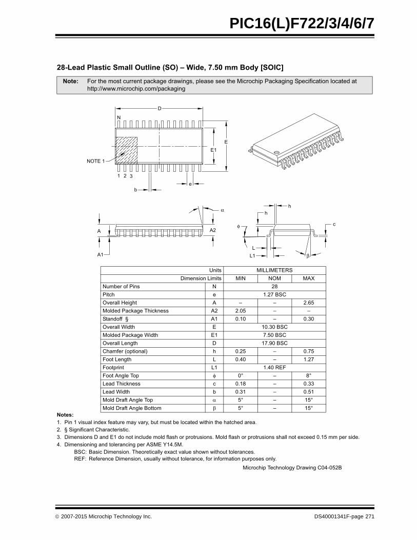
PIC16(L)F722/3/4/6/7
������������������0���� ��0��1���'2-.��������0�/
!����"�� ������ �!"�����#�$�%��&"��'��� ��(�)"&�'"!&�)�����&�#�*�&����&�����&���#������� +������%����&�,����&��!&���-� ��'��!��!�����#�.��#��&�����"#��'�#�%��!����&"!��!����#�%��!����&"!��!�!������&��$���#������''����!�#���� ��'��!��������#�&���������������.�0������
1�,2 1�!�����'��!���� ���&��������$��&� ��"��!�*��*�&�"&�&������!��.32 ��%��������'��!��(�"!"�����*�&�"&�&������(�%���%'�&����"�!�!�����
!���" 3�&���'!&��"��&����4����#�*���!(�����!��!���&��������������4�����������%���&������&�#��&��&&�255***�'��������'5���4�����
6��&! ��99��. .����'��!���9�'�&! ��7 7:� ��;
7"')��%����! 7 �<��&�� � �����1�,: �����8����& � = = ��?���#�#����4���� ���4��!! �� ���� = =�&��#%%��+ �� ���� = ��-�: �����>�#&� . ���-��1�,��#�#����4����>�#&� .� �����1�,: �����9���&� � ������1�,,��'%��A�&����B � ���� = ����3&�9���&� 9 ���� = ����3&���& 9� ������.33&������� � � �C = <C9��#� ���4��!! � ���< = ��--9��#�>�#&� ) ��-� = ������#���%&������� � � �C = ��C��#���%&�������1&&' � �C = ��C
c
h
h
L
L1
A2
A1
A
NOTE 1
1 2 3
b
e
E
E1
D
φ
β
α
N
������� ������� ��*��� ,������1
2007-2015 Microchip Technology Inc. DS40001341F-page 271

PIC16(L)F722/3/4/6/7
��������������,3� �����0���� ����.-���������0�
!����"�� ������ �!"�����#�$�%��&"��'��� ��(�)"&�'"!&�)�����&�#�*�&����&�����&���#������� ��'��!��!�����#�.��#��&�����"#��'�#�%��!����&"!��!����#�%��!����&"!��!�!������&��$���#������''����!�#��-� ��'��!��������#�&���������������.�0������
1�,2 1�!�����'��!���� ���&��������$��&� ��"��!�*��*�&�"&�&������!��.32 ��%��������'��!��(�"!"�����*�&�"&�&������(�%���%'�&����"�!�!�����
!���" 3�&���'!&��"��&����4����#�*���!(�����!��!���&��������������4�����������%���&������&�#��&��&&�255***�'��������'5���4�����
6��&! ��99��. .����'��!���9�'�&! ��7 7:� ��;
7"')��%����! 7 �<��&�� � ��?��1�,: �����8����& � = = ������#�#����4���� ���4��!! �� ��?� ���� ��<��&��#%%� �� ���� = =: �����>�#&� . ���� ��<� <�����#�#����4����>�#&� .� ���� ��-� ��?�: �����9���&� � ���� ����� �����3&�9���&� 9 ���� ���� ����3&���& 9� ������.39��#� ���4��!! � ���� = ����3&������ � �C �C <C9��#�>�#&� ) ���� = ��-<
LL1
c
A2
A1
A
E
E1
D
N
1 2
NOTE 1b
e
φ
������� ������� ��*��� ,�����-1
DS40001341F-page 272 2007-2015 Microchip Technology Inc.

PIC16(L)F722/3/4/6/7
##������������4,� %���&���5�����4��6�*6�*6������'�-�����4%&�
!����"�� ������ �!"�����#�$�%��&"��'��� ��(�)"&�'"!&�)�����&�#�*�&����&�����&���#������� ,��'%�!��&����!�����&����D�!�E��'��� ���-� ��'��!��!������#�.��#��&�����"#��'�#�%��!����&"!��!����#�%��!����&"!��!�!������&��$���#������''����!�#���� ��'��!��������#�&���������������.�0������
1�,2 1�!�����'��!���� ���&��������$��&� ��"��!�*��*�&�"&�&������!��.32 ��%��������'��!��(�"!"�����*�&�"&�&������(�%���%'�&����"�!�!�����
!���" 3�&���'!&��"��&����4����#�*���!(�����!��!���&��������������4�����������%���&������&�#��&��&&�255***�'��������'5���4�����
6��&! ��99��. .����'��!���9�'�&! ��7 7:� ��;
7"')��%�9��#! 7 ��9��#���&�� � ��<��1�,: �����8����& � = = ������#�#����4���� ���4��!! �� ���� ���� �����&��#%%�� �� ���� = ����3&�9���&� 9 ���� ��?� ����3&���& 9� ������.33&������ � �C -��C �C: �����>�#&� . ������1�,: �����9���&� � ������1�,��#�#����4����>�#&� .� ������1�,��#�#����4����9���&� �� ������1�,9��#� ���4��!! � ���� = ����9��#�>�#&� ) ��-� ��-� ������#���%&������� � � ��C ��C �-C��#���%&�������1&&' � ��C ��C �-C
A
E
E1
D
D1
e
b
NOTE 1NOTE 2
N
1 2 3
c
A1L
A2L1
α
φ
β
������� ������� ��*��� ,�����?1
2007-2015 Microchip Technology Inc. DS40001341F-page 273

PIC16(L)F722/3/4/6/7
##������������4,� %���&���5�����4��6�*6�*6������'�-�����4%&�
!���" 3�&���'!&��"��&����4����#�*���!(�����!��!���&��������������4�����������%���&������&�#��&��&&�255***�'��������'5���4�����
DS40001341F-page 274 2007-2015 Microchip Technology Inc.

PIC16(L)F722/3/4/6/7
Note: For the most current package drawings, please see the Microchip Packaging Specification located at
http://www.microchip.com/packaging
2007-2015 Microchip Technology Inc. DS40001341F-page 275

PIC16(L)F722/3/4/6/7
Note: For the most current package drawings, please see the Microchip Packaging Specification located at
http://www.microchip.com/packaging
DS40001341F-page 276 2007-2015 Microchip Technology Inc.

2007-2015 Microchip Technology Inc. DS40001341F-page 277
PIC16(L)F722/3/4/6/7
APPENDIX A: DATA SHEET REVISION HISTORY
Revision A (12/2007)
Original release.
Revision B (08/2008)
Electrical Specification updates; Package Drawings;miscellaneous updates.
Revision C (04/2009)
Revised data sheet title; Revised Low-Power Featuressection; Revised Section 6.2.2.4 RA3/AN3/VREF;Revised Figure 16-8 Synchronous Reception.
Revision D (07/2009)
Removed the Preliminary Label; Updated the“Electrical Characteristics” section; Added charts in the“Char. Data” section; Deleted “Based 8-Bit CMOS”from title; Updated the “Special MicrocontrollerFeatures” section and the “Peripheral Features”section; Changed the title of the “Low Power Features”section into “Extreme Low-Power ManagementPIC16LF72X with nanoWatt XLP” and updated thissection; Inserted new section – “Analog Features”(page 1); Changed the title of the “Peripheral Features”section into “Peripheral Highlights” and updated thesection.
Revision E (10/2009)
Added paragraph to section 5.0 (LDO VoltageRegulator); Updated the Electrical Specificationssection (Added another absolute Maximum Rating;Updated section 23.1 and Table 23-4); Updated the PinDiagrams with the UQFN package; Updated Table 1,adding UQFN; Updated section 23.5 (ThermalConsiderations); Updated the Packaging Informationsection adding the UQFN Package; Updated theProduct Identification System section.
Revision F (12/2015)
Updated Table 2; Updated 23.1, 23.3 and 9.2.4Sections; Updated Figure 23-9; Other minorcorrections.
APPENDIX B: MIGRATING FROM OTHER PIC® DEVICES
This discusses some of the issues in migrating fromother PIC® devices to the PIC16F72X family ofdevices.
B.1 PIC16F77 to PIC16F72X
TABLE B-1: FEATURE COMPARISON
Feature PIC16F77 PIC16F727
Max. Operating Speed 20 MHz 20 MHz
Max. Program Memory (Words)
8K 8K
Max. SRAM (Bytes) 368 368
A/D Resolution 8-bit 8-bit
Timers (8/16-bit) 2/1 2/1
Oscillator Modes 4 8
Brown-out Reset Y Y
Internal Pull-ups RB<7:0> RB<7:0>
Interrupt-on-change RB<7:4> RB<7:0>
Comparator 0 0
USART Y Y
Extended WDT N N
Software Control Option of WDT/BOR
N N
INTOSC Frequencies None 500 kHz - 16 MHz
Clock Switching N N

PIC16(L)F722/3/4/6/7
DS40001341F-page 278 2007-2015 Microchip Technology Inc.
THE MICROCHIP WEBSITE
Microchip provides online support via our website atwww.microchip.com. This website is used as a meansto make files and information easily available tocustomers. Accessible by using your favorite Internetbrowser, the website contains the following information:
• Product Support – Data sheets and errata, appli-cation notes and sample programs, design resources, user’s guides and hardware support documents, latest software releases and archived software
• General Technical Support – Frequently Asked Questions (FAQ), technical support requests, online discussion groups, Microchip consultant program member listing
• Business of Microchip – Product selector and ordering guides, latest Microchip press releases, listing of seminars and events, listings of Micro-chip sales offices, distributors and factory repre-sentatives
CUSTOMER CHANGE NOTIFICATION SERVICE
Microchip’s customer notification service helps keepcustomers current on Microchip products. Subscriberswill receive e-mail notification whenever there arechanges, updates, revisions or errata related to a spec-ified product family or development tool of interest.
To register, access the Microchip website atwww.microchip.com. Under “Support”, click on “Cus-tomer Change Notification” and follow the registrationinstructions.
CUSTOMER SUPPORT
Users of Microchip products can receive assistancethrough several channels:
• Distributor or Representative
• Local Sales Office
• Field Application Engineer (FAE)
• Technical Support
Customers should contact their distributor, representa-tive or Field Application Engineer (FAE) for support.Local sales offices are also available to help custom-ers. A listing of sales offices and locations is included inthe back of this document.
Technical support is available through the websiteat: http://www.microchip.com/support

PIC16(L)F722/3/4/6/7
PRODUCT IDENTIFICATION SYSTEM
To order or obtain information, e.g., on pricing or delivery, refer to the factory or the listed sales office.
PART NO. X /XX XXX
PatternPackageTemperatureRange
Device
Device: PIC16F722, PIC16LF722, PIC16F722T, PIC16LF722T(1)
PIC16F723, PIC16LF723, PIC16F723T, PIC16LF723T(1)
PIC16F724, PIC16LF724, PIC16F724T, PIC16LF724T(1)
PIC16F726, PIC16LF726, PIC16F726T, PIC16LF726T(1)
PIC16F727, PIC16LF727, PIC16F727T, PIC16LF727T(1)
Tape and Reel Option:
I = -40C to +85CE = -40C to +125CMV = Micro Lead Frame (UQFN)
Temperature Range:
I = -40C to +85C (Industrial)E = -40C to +125C (Extended)
Package: ML = Micro Lead Frame (QFN)P = Plastic DIPPT = TQFP (Thin Quad Flatpack)SO = SOICSP = Skinny Plastic DIPSS = SSOP
Examples:
a) PIC16F722-E/SP 301 = Extended Temp.,skinny PDIP package, QTP pattern #301
b) PIC16F722-I/SO = Industrial Temp., SOIC package
Note 1: Tape and Reel identifier only appears in the catalog part number description. This identifier is used for ordering purposes and is not printed on the device package. Check with your Microchip Sales Office for package availability with the Tape and Reel option.
[X](1)
Tape and ReelOption
2007-2015 Microchip Technology Inc. DS40001341F-page 279

PIC16(L)F722/3/4/6/7
NOTES:
DS40001341F-page 280 2007-2015 Microchip Technology Inc.

Note the following details of the code protection feature on Microchip devices:
• Microchip products meet the specification contained in their particular Microchip Data Sheet.
• Microchip believes that its family of products is one of the most secure families of its kind on the market today, when used in the intended manner and under normal conditions.
• There are dishonest and possibly illegal methods used to breach the code protection feature. All of these methods, to our knowledge, require using the Microchip products in a manner outside the operating specifications contained in Microchip’s Data Sheets. Most likely, the person doing so is engaged in theft of intellectual property.
• Microchip is willing to work with the customer who is concerned about the integrity of their code.
• Neither Microchip nor any other semiconductor manufacturer can guarantee the security of their code. Code protection does not mean that we are guaranteeing the product as “unbreakable.”
Code protection is constantly evolving. We at Microchip are committed to continuously improving the code protection features of ourproducts. Attempts to break Microchip’s code protection feature may be a violation of the Digital Millennium Copyright Act. If such actsallow unauthorized access to your software or other copyrighted work, you may have a right to sue for relief under that Act.
Information contained in this publication regarding deviceapplications and the like is provided only for your convenienceand may be superseded by updates. It is your responsibility toensure that your application meets with your specifications.MICROCHIP MAKES NO REPRESENTATIONS ORWARRANTIES OF ANY KIND WHETHER EXPRESS ORIMPLIED, WRITTEN OR ORAL, STATUTORY OROTHERWISE, RELATED TO THE INFORMATION,INCLUDING BUT NOT LIMITED TO ITS CONDITION,QUALITY, PERFORMANCE, MERCHANTABILITY ORFITNESS FOR PURPOSE. Microchip disclaims all liabilityarising from this information and its use. Use of Microchipdevices in life support and/or safety applications is entirely atthe buyer’s risk, and the buyer agrees to defend, indemnify andhold harmless Microchip from any and all damages, claims,suits, or expenses resulting from such use. No licenses areconveyed, implicitly or otherwise, under any Microchipintellectual property rights unless otherwise stated.
2007-2015 Microchip Technology Inc.
QUALITY MANAGEMENT SYSTEM CERTIFIED BY DNV
== ISO/TS 16949 ==
Trademarks
The Microchip name and logo, the Microchip logo, dsPIC, FlashFlex, flexPWR, JukeBlox, KEELOQ, KEELOQ logo, Kleer, LANCheck, MediaLB, MOST, MOST logo, MPLAB, OptoLyzer, PIC, PICSTART, PIC32 logo, RightTouch, SpyNIC, SST, SST Logo, SuperFlash and UNI/O are registered trademarks of Microchip Technology Incorporated in the U.S.A. and other countries.
The Embedded Control Solutions Company and mTouch are registered trademarks of Microchip Technology Incorporated in the U.S.A.
Analog-for-the-Digital Age, BodyCom, chipKIT, chipKIT logo, CodeGuard, dsPICDEM, dsPICDEM.net, ECAN, In-Circuit Serial Programming, ICSP, Inter-Chip Connectivity, KleerNet, KleerNet logo, MiWi, motorBench, MPASM, MPF, MPLAB Certified logo, MPLIB, MPLINK, MultiTRAK, NetDetach, Omniscient Code Generation, PICDEM, PICDEM.net, PICkit, PICtail, RightTouch logo, REAL ICE, SQI, Serial Quad I/O, Total Endurance, TSHARC, USBCheck, VariSense, ViewSpan, WiperLock, Wireless DNA, and ZENA are trademarks of Microchip Technology Incorporated in the U.S.A. and other countries.
SQTP is a service mark of Microchip Technology Incorporated in the U.S.A.
Silicon Storage Technology is a registered trademark of Microchip Technology Inc. in other countries.
GestIC is a registered trademark of Microchip Technology Germany II GmbH & Co. KG, a subsidiary of Microchip Technology Inc., in other countries.
All other trademarks mentioned herein are property of their respective companies.
© 2007-2015, Microchip Technology Incorporated, Printed in the U.S.A., All Rights Reserved.
ISBN: 978-1-5224-0042-4
Microchip received ISO/TS-16949:2009 certification for its worldwide
DS40001341F-page 281
headquarters, design and wafer fabrication facilities in Chandler and Tempe, Arizona; Gresham, Oregon and design centers in California and India. The Company’s quality system processes and procedures are for its PIC® MCUs and dsPIC® DSCs, KEELOQ® code hopping devices, Serial EEPROMs, microperipherals, nonvolatile memory and analog products. In addition, Microchip’s quality system for the design and manufacture of development systems is ISO 9001:2000 certified.

DS40001341F-page 282 2007-2015 Microchip Technology Inc.
AMERICASCorporate Office2355 West Chandler Blvd.Chandler, AZ 85224-6199Tel: 480-792-7200 Fax: 480-792-7277Technical Support: http://www.microchip.com/supportWeb Address: www.microchip.com
AtlantaDuluth, GA Tel: 678-957-9614 Fax: 678-957-1455
Austin, TXTel: 512-257-3370
BostonWestborough, MA Tel: 774-760-0087 Fax: 774-760-0088
ChicagoItasca, IL Tel: 630-285-0071 Fax: 630-285-0075
ClevelandIndependence, OH Tel: 216-447-0464 Fax: 216-447-0643
DallasAddison, TX Tel: 972-818-7423 Fax: 972-818-2924
DetroitNovi, MI Tel: 248-848-4000
Houston, TX Tel: 281-894-5983
IndianapolisNoblesville, IN Tel: 317-773-8323Fax: 317-773-5453
Los AngelesMission Viejo, CA Tel: 949-462-9523 Fax: 949-462-9608
New York, NY Tel: 631-435-6000
San Jose, CA Tel: 408-735-9110
Canada - TorontoTel: 905-673-0699 Fax: 905-673-6509
ASIA/PACIFICAsia Pacific OfficeSuites 3707-14, 37th FloorTower 6, The GatewayHarbour City, Kowloon
Hong KongTel: 852-2943-5100Fax: 852-2401-3431
Australia - SydneyTel: 61-2-9868-6733Fax: 61-2-9868-6755
China - BeijingTel: 86-10-8569-7000 Fax: 86-10-8528-2104
China - ChengduTel: 86-28-8665-5511Fax: 86-28-8665-7889
China - ChongqingTel: 86-23-8980-9588Fax: 86-23-8980-9500
China - DongguanTel: 86-769-8702-9880
China - HangzhouTel: 86-571-8792-8115 Fax: 86-571-8792-8116
China - Hong Kong SARTel: 852-2943-5100 Fax: 852-2401-3431
China - NanjingTel: 86-25-8473-2460Fax: 86-25-8473-2470
China - QingdaoTel: 86-532-8502-7355Fax: 86-532-8502-7205
China - ShanghaiTel: 86-21-5407-5533 Fax: 86-21-5407-5066
China - ShenyangTel: 86-24-2334-2829Fax: 86-24-2334-2393
China - ShenzhenTel: 86-755-8864-2200 Fax: 86-755-8203-1760
China - WuhanTel: 86-27-5980-5300Fax: 86-27-5980-5118
China - XianTel: 86-29-8833-7252Fax: 86-29-8833-7256
ASIA/PACIFICChina - XiamenTel: 86-592-2388138 Fax: 86-592-2388130
China - ZhuhaiTel: 86-756-3210040 Fax: 86-756-3210049
India - BangaloreTel: 91-80-3090-4444 Fax: 91-80-3090-4123
India - New DelhiTel: 91-11-4160-8631Fax: 91-11-4160-8632
India - PuneTel: 91-20-3019-1500
Japan - OsakaTel: 81-6-6152-7160 Fax: 81-6-6152-9310
Japan - TokyoTel: 81-3-6880- 3770 Fax: 81-3-6880-3771
Korea - DaeguTel: 82-53-744-4301Fax: 82-53-744-4302
Korea - SeoulTel: 82-2-554-7200Fax: 82-2-558-5932 or 82-2-558-5934
Malaysia - Kuala LumpurTel: 60-3-6201-9857Fax: 60-3-6201-9859
Malaysia - PenangTel: 60-4-227-8870Fax: 60-4-227-4068
Philippines - ManilaTel: 63-2-634-9065Fax: 63-2-634-9069
SingaporeTel: 65-6334-8870Fax: 65-6334-8850
Taiwan - Hsin ChuTel: 886-3-5778-366Fax: 886-3-5770-955
Taiwan - KaohsiungTel: 886-7-213-7828
Taiwan - TaipeiTel: 886-2-2508-8600 Fax: 886-2-2508-0102
Thailand - BangkokTel: 66-2-694-1351Fax: 66-2-694-1350
EUROPEAustria - WelsTel: 43-7242-2244-39Fax: 43-7242-2244-393
Denmark - CopenhagenTel: 45-4450-2828 Fax: 45-4485-2829
France - ParisTel: 33-1-69-53-63-20 Fax: 33-1-69-30-90-79
Germany - DusseldorfTel: 49-2129-3766400
Germany - KarlsruheTel: 49-721-625370
Germany - MunichTel: 49-89-627-144-0 Fax: 49-89-627-144-44
Italy - Milan Tel: 39-0331-742611 Fax: 39-0331-466781
Italy - VeniceTel: 39-049-7625286
Netherlands - DrunenTel: 31-416-690399 Fax: 31-416-690340
Poland - WarsawTel: 48-22-3325737
Spain - MadridTel: 34-91-708-08-90Fax: 34-91-708-08-91
Sweden - StockholmTel: 46-8-5090-4654
UK - WokinghamTel: 44-118-921-5800Fax: 44-118-921-5820
Worldwide Sales and Service
07/14/15