Embed Size (px)
Citation preview
Output C
ompar
16
Section 16. Output Compare
e
HIGHLIGHTSThis section of the manual contains the following major topics:
16.1 Introduction .................................................................................................................. 16-216.2 Output Compare Registers ..........................................................................................16-316.3 Operation ..................................................................................................................... 16-616.4 Interrupts.................................................................................................................... 16-3316.5 I/O Pin Control ...........................................................................................................16-3416.6 Operation In Power-Saving and Debug Modes ......................................................... 16-3516.7 Effects of Various Resets ...........................................................................................16-3516.8 Output Compare Application......................................................................................16-3616.9 Design Tips ................................................................................................................ 16-3816.10 Related Application Notes.......................................................................................... 16-3916.11 Revision History .........................................................................................................16-40
© 2011 Microchip Technology Inc. DS61111E-page 16-1

PIC32 Family Reference Manual
16.1 INTRODUCTIONThe Output Compare module is primarily used to generate a single pulse or a series of pulses in response to selected time base events.
The following are some of the key features of the Output Compare module:
• Multiple Output Compare modules in a device• Single and Dual Compare modes• Single and continuous output pulse generation• Pulse-Width Modulation (PWM) mode• Programmable interrupt generation on compare event• Hardware-based PWM Fault detection and automatic output disable• Programmable selection of 16 or 32-bit time bases• Operate from either of two available 16-bit time bases or a single 32-bit time base
Figure 16-1 illustrates the block diagram of an Output Compare module.
Figure 16-1: Output Compare Module Block Diagram
Note: This family reference manual section is meant to serve as a complement to device data sheets. Depending on the device variant, this manual section may not apply to all PIC32 devices.
Please consult the note at the beginning of the “Output Compare” chapter in the current device data sheet to check whether this document supports the device you are using.
Device data sheets and family reference manual sections are available for download from the Microchip Worldwide Web site at: http://www.microchip.com
OCxR(1)
Comparator
OutputLogic
QSR
OCM<2:0>
Output Enable
OCx(1)
Set Flag bitOCxIF(1)
OCxRS(1)
Mode Select
3
Note 1: Where ‘x’ is shown, reference is made to the registers associated with the respective output compare channels 1 through 5.
2: OCFA pin controls OC1-OC4 channels. OCFB pin controls OC5 channels.3: Each output compare channel can use one of two selectable 16-bit time bases or a single 32-bit time base.
Refer to the specific device data sheet for the time bases associated with the module.
0 1 OCTSEL 0 1
16 16
OCFA or OCFB(2)
TMR register inputsfrom time bases(3)
Period match signalsfrom time bases(3)
DS61111E-page 16-2 © 2011 Microchip Technology Inc.

Section 16. Output CompareO
utput Com
pare
16
16.2 OUTPUT COMPARE REGISTERSEach Output Compare module consists of the following Special Function Registers (SFRs):
• OCxCON: Output Compare ‘x’ Control Register• OCxR: Output Compare ‘x’ Compare Register• OCxRS: Output Compare ‘x’ Secondary Compare Register
Table 16-1 summarizes all output compare related registers. Corresponding registers appear after the summary, followed by a detailed description of each register.
Note: Each PIC32 family device variant may have one or more Output Compare modules. An ‘x’ used in the names of pins, control/status bits and registers denotes the particular module. Refer to the specific device data sheets for more details.
Table 16-1: Output Compare SFR Summary
Name Bit31/23/15/7
Bit30/22/14/6
Bit29/21/13/5
Bit28/20/12/4
Bit27/19/11/3
Bit26/18/10/2
Bit25/17/9/1
Bit24/16/8/0
OCxCON(1,2,3) 31:24 — — — — — — — —
23:16 — — — — — — — —
15:8 ON — SIDL — — — — —
7:0 — — OC32 OCFLT OCTSEL OCM<2:0>
OCxR(1,2,3) 31:24 OCxR<31:24>
23:16 OCxR<23:16>
15:8 OCxR<15:8>
7:0 OCxR<7:0>
OCxRS(1,2,3) 31:24 OCxRS<31:24>
23:16 OCxRS<23:16>
15:8 OCxRS<15:8>
7:0 OCxRS<7:0>
Legend: — = unimplemented, read as ‘0’. Note 1: This register has an associated Clear register at an offset of 0x4 bytes. The Clear register has the same name with CLR
appended to the register name (e.g., OCxCONCLR). Writing a ‘1’ to any bit position in the Clear register will clear valid bits in the associated register. Reads from the Clear register should be ignored.
2: This register has an associated Set register at an offset of 0x8 bytes. The Set register has the same name with SET appended to the register name (e.g., OCxCONSET). Writing a ‘1’ to any bit position in the Set register will set valid bits in the associated register. Reads from the Set register should be ignored.
3: This register has an associated Invert register at an offset of 0xC bytes. The Invert register has the same name with INV appended to the register name (e.g., OCxCONINV). Writing a ‘1’ to any bit position in the Invert register will invert valid bits in the associated register. Reads from the Invert register should be ignored.
© 2011 Microchip Technology Inc. DS61111E-page 16-3

PIC32 Family Reference Manual
Register 16-1: OCxCON: Output Compare ‘x’ Control Register Bit
RangeBit
31/23/15/7Bit
30/22/14/6Bit
29/21/13/5Bit
28/20/12/4Bit
27/19/11/3Bit
26/18/10/2Bit
25/17/9/1Bit
24/16/8/0
31:24U-0 U-0 U-0 U-0 U-0 U-0 U-0 U-0— — — — — — — —
23:16U-0 U-0 U-0 U-0 U-0 U-0 U-0 U-0— — — — — — — —
15:8R/W-0 U-0 R/W-0 U-0 U-0 U-0 U-0 U-0ON(1) — SIDL — — — — —
7:0U-0 U-0 R/W-0 R-0 R/W-0 R/W-0 R/W-0 R/W-0— — OC32 OCFLT(2) OCTSEL OCM<2:0>
Legend:R = Readable bit W = Writable bit U = Unimplemented bit, read as ‘0’-n = Value at POR ‘1’ = Bit is set ‘0’ = Bit is cleared x = Bit is unknown
bit 31-16 Unimplemented: Read as ‘0’bit 15 ON: Output Compare Peripheral On bit(1)
1 = Output compare peripheral is enabled 0 = Output compare peripheral is disabled and not drawing current. SFR modifications are allowed. The
status of other bits in this register are not affected by setting or clearing this bitbit 14 Unimplemented: Read as ‘0’bit 13 SIDL: Stop in Idle Mode bit
1 = Discontinue operation when CPU enters Idle mode0 = Continue operation in Idle mode
bit 12-6 Unimplemented: Read as ‘0’bit 5 OC32: 32-bit Compare Mode bit
1 = OCxR<31:0> and/or OCxRS<31:0> is used for comparisions to the 32-bit timer source0 = OCxR<15:0> and OCxRS<15:0> are used for comparisons to the 16-bit timer source
bit 4 OCFLT: PWM Fault Condition Status bit(2)
1 = PWM Fault condition has occurred (cleared in hardware only)0 = No PWM Fault condition has occurred
bit 3 OCTSEL: Output Compare Timer Select bit1 = Timer3 is the clock source for this Output Compare module0 = Timer2 is the clock source for this Output Compare moduleRefer to the specific device data sheet for the time bases that are available to the Output Compare module.
bit 2-0 OCM<2:0>: Output Compare Mode Select bits111 = PWM mode on OCx; Fault pin enabled110 = PWM mode on OCx; Fault pin disabled101 = Initialize OCx pin low; generate continuous output pulses on OCx pin100 = Initialize OCx pin low; generate single output pulse on OCx pin011 = Compare event toggles OCx pin010 = Initialize OCx pin high; compare event forces OCx pin low001 = Initialize OCx pin low; compare event forces OCx pin high000 = Output compare peripheral is disabled but continues to draw current
Note 1: When using 1:1 PBCLK divisor, the user’s software should not read/write the peripheral’s SFRs in the SYSCLK cycle immediately following the instruction that clears the module’s ON bit.
2: This bit is only used when OCM<2:0> = 111 and reads as ‘0’ in modes other than PWM mode.
DS61111E-page 16-4 © 2011 Microchip Technology Inc.

Section 16. Output CompareO
utput Com
pare
16
Register 16-2: OCxR: Output Compare ‘x’ Compare RegisterBit Range
Bit31/23/15/7
Bit30/22/14/6
Bit29/21/13/5
Bit28/20/12/4
Bit27/19/11/3
Bit26/18/10/2
Bit25/17/9/1
Bit24/16/8/0
31:24R/W-0 R/W-0 R/W-0 R/W-0 R/W-0 R/W-0 R/W-0 R/W-0
OCR<31:24>
23:16R/W-0 R/W-0 R/W-0 R/W-0 R/W-0 R/W-0 R/W-0 R/W-0
OCR<23:16>
15:8R/W-0 R/W-0 R/W-0 R/W-0 R/W-0 R/W-0 R/W-0 R/W-0
OCR<15:8>
7:0R/W-0 R/W-0 R/W-0 R/W-0 R/W-0 R/W-0 R/W-0 R/W-0
OCR<7:0>
Legend:R = Readable bit W = Writable bit U = Unimplemented bit, read as ‘0’-n = Value at POR ‘1’ = Bit is set ‘0’ = Bit is cleared x = Bit is unknown
bit 31-16 OCxR<31:16>: Upper 16 bits of 32-bit compare value, when OC32 (OCxCON<5>) = 1bit 15-0 OCxR<15:0>: Lower 16 bits of 32-bit compare value or entire 16 bits of 16-bit compare value when
OC32 = 0
Register 16-3: OCxRS: Output Compare ‘x’ Secondary Compare RegisterBit
RangeBit
31/23/15/7Bit
30/22/14/6Bit
29/21/13/5Bit
28/20/12/4Bit
27/19/11/3Bit
26/18/10/2Bit
25/17/9/1Bit
24/16/8/0
31:24R/W-0 R/W-0 R/W-0 R/W-0 R/W-0 R/W-0 R/W-0 R/W-0
OCRS<31:24>
23:16R/W-0 R/W-0 R/W-0 R/W-0 R/W-0 R/W-0 R/W-0 R/W-0
OCRS<23:16>
15:8R/W-0 R/W-0 R/W-0 R/W-0 R/W-0 R/W-0 R/W-0 R/W-0
OCRS<15:8>
7:0R/W-0 R/W-0 R/W-0 R/W-0 R/W-0 R/W-0 R/W-0 R/W-0
OCRS<7:0>
Legend:R = Readable bit W = Writable bit U = Unimplemented bit, read as ‘0’-n = Value at POR ‘1’ = Bit is set ‘0’ = Bit is cleared x = Bit is unknown
bit 31-16 OCxRS<31:16>: Upper 16 bits of 32-bit compare value when OC32 (OCxCON<5>) = 1bit 15-0 OCxRS<15:0>: Lower 16 bits of 32-bit compare value or entire 16 bits of 16-bit compare value when
OC32 = 0
© 2011 Microchip Technology Inc. DS61111E-page 16-5

PIC32 Family Reference Manual
16.3 OPERATIONEach Output Compare module has the following modes of operation:
• Single Compare Match mode- With output drive high- With output drive low- With output drive toggles
• Dual Compare Match mode- With single output pulse- With continuous output pulses
• Simple Pulse-Width Modulation mode - Without Fault protection input- With Fault protection input
16.3.1 Single Compare Match ModeWhen the OCM<2:0> control bits (OCxCON<2:0>) are set to ‘001’, ‘010’ or ‘011’, the selected output compare channel is configured for one of three Single Output Compare Match modes. The compare time base must also be enabled.
In the Single Compare mode, the OCxR register is loaded with a value and is compared to the selected incrementing timer register, TMRy. On a compare match event, one of the following events will take place:
• Compare forces OCx pin high; initial state of pin is low. Interrupt is generated on the single compare match event.
• Compare forces OCx pin low; initial state of pin is high. Interrupt is generated on the single compare match event.
• Compare toggles OCx pin. Toggle event is continuous and an interrupt is generated for each toggle event.
Note 1: The Output Compare module must be turned OFF by the user application (i.e., clear the OCM<2:0> bits (OCxCON<2:0>)) before switching to a new mode. Changing modes while the module is in operation may produce unexpected results.
2: In this section, a reference to any SFRs associated with the selected timer source is indicated by a ‘y’ suffix. For example, PR2 is the Period register for the selected timer source, while TyCON is the Timer Control register for the selected timer source.
DS61111E-page 16-6 © 2011 Microchip Technology Inc.

Section 16. Output CompareO
utput Com
pare
16
16.3.1.1 Compare Mode Output Driven HighTo configure the Output Compare module for this mode, set the OCM<2:0> control bits to ‘001’.The compare time base must also be enabled. Once this mode has been enabled, the output pin, OCx, will be driven low and remain low until a match occurs between the TMRy and OCxR registers. In Figure 16-2, note the following key timing events:
• The OCx pin is driven high one peripheral clock after the compare match occurs between the compare time base and the OCxR register. The OCx pin will remain high until a mode change has been made or the module is disabled.
• The compare time base will count up to the value contained in the associated period register, and then reset to 0x0000 on the next PBCLK
• The respective channel interrupt flag, OCxIF (see the IFS0 register for the position of the interrupt flag bit for each of the output compare channels), is asserted when the OCx pin is driven high
Figure 16-2: Single Compare Mode: Set OCx High on Compare Match Event (16-Bit Mode)
Figure 16-3: Single Compare Mode: Set OCx High on Compare Match Event (32-Bit Mode)
OCxIF
4000 00013001 3002 3003 30043000TMRy 0000
Cleared by User
1 PBCLK Period
4000
3002
PRy
OCxR
3FFF
OCx pin
TMRy Resets Here
Note: An ‘x’ represents the output compare channel number. A ‘y’ represents the time base number.
OCxIF
0004: 0000:0003: 0003: 0003: 0003:0003:TMRy 0000:
Cleared by User
1 PBCLK Period
0004:
0003:
PRy
OCxR
0003:
OCx pin
TMRy Resets Here
Note: An ‘x’ represents the output compare channel number. A ‘y’ represents the time base number.
0002
0000 0001 0002 0003 0004
0000
0000FFFF 0000 0001
© 2011 Microchip Technology Inc. DS61111E-page 16-7

PIC32 Family Reference Manual
16.3.1.2 Compare Mode Output Driven Low
To configure the Output Compare module for this mode, set the OCM<2:0> control bits to ‘010’.The compare time base must also be enabled. Once this mode has been enabled, the output pin, OCx, will be driven high and remain high until a match occurs between the Timer and OCxR registers. In Figure 16-4, note the following key timing events:
• The OCx pin is driven low by one PBCLK after the compare match occurs between the compare time base and the OCxR register. The OCx pin will remain low until a mode change has been made or the module is disabled.
• The compare time base will count up to the value contained in the associated period register, and then reset to 0x0000 on the next PBCLK
• The respective channel interrupt flag, OCxIF, is asserted when the OCx pin is driven low
Figure 16-4: Single Compare Mode: Force OCx Low on Compare Match Event (16-Bit Mode)
Figure 16-5: Single Compare Mode: Set OCx Low on Compare Match Event (32-Bit Mode)
OCxIF
4C00 000147FF 4800 4801 480247FETMRy 0000
Cleared by User
1 PBCLK Period
4C00
4800
PRy
OCxR
4BFF
OCx pin
TMRy Resets Here
Note: An ‘x’ represents the output compare channel number. A ‘y’ represents the time base number.
OCxIF
0004: 0000:0003: 0003: 0003: 0003:0003:TMRy 0000:
Cleared by User
1 PBCLK Period
0004:
0003:
PRy
OCxR
0003:
OCx pin
TMRy Resets Here
Note: An ‘x’ represents the output compare channel number. A ‘y’ represents the time base number.
0002
0000 0001 0002 0003 0004
0000
0000FFFF 0000 0001
DS61111E-page 16-8 © 2011 Microchip Technology Inc.

Section 16. Output CompareO
utput Com
pare
16
16.3.1.3 Single Compare Mode Toggle OutputTo configure the Output Compare module for this mode, set the OCM<2:0> control bits to ‘011’.In addition, Timer2 or Timer3 must be selected and enabled. Once this mode has been enabled, the output pin, OCx, will be initially driven low, and then toggle on each and every subsequent match event between the Timer and OCxR registers. In Figure 16-6 and Figure 16-8, note the following key timing events:
• The OCx pin is toggled one PBCLK after the compare match occurs between the compare time base and the OCxR register. The OCx pin will remain at this new state until the next toggle event, or until a mode change has been made or the module is disabled.
• The compare time base will count up to the contents in the period register, and then reset to 0x0000 on the next PBCLK
• The respective channel interrupt flag, OCxIF, is asserted when the OCx pin is toggled
Figure 16-6: Single Compare Mode: Toggle Output on Compare Match Event (16-Bit Mode)
Figure 16-7: Single Compare Mode: Toggle Output on Compare Match Event (32-Bit Mode)
Note: The internal OCx pin output logic is set to a logic ‘0’ on a device Reset. However, the operational OCx pin state for the Toggle mode can be set by the user application.Example 16-1 shows a code example for defining the desired initial OCx pin state in the Toggle mode of operation.
OCxIF
05000501 0502 06000500TMRy
1 PBCLK Period
0600
0500
PRy
OCxR
0001
OCx pin
TMRy Resets Here
0000 0501 0502
Cleared by User
Note: An ‘x’ represents the output compare channel number. A ‘y’ represents the time base number.
OCxIF
0005:0005: 0005: 0000:0006:0005:TMRy 0005:
Cleared by User
1 PBCLK Period
0006:
0005:
PRy
OCxR
0000:
OCx pin
TMRy Resets Here
Note: An ‘x’ represents the output compare channel number. A ‘y’ represents the time base number.
0000
0000 0001 0002 00000000
0000
0001 0000 0001
© 2011 Microchip Technology Inc. DS61111E-page 16-9

PIC32 Family Reference Manual
Figure 16-8: Single Compare Mode: Toggle Output on Compare Match Event (PRy = OCxR, 16-Bit Mode)
Figure 16-9: Single Compare Mode: Toggle Output on Compare Match Event (PRy = OCxR, 32-Bit Mode)
Example 16-1: Compare Mode Toggle Mode Pin State Setup (16-Bit Mode)
OCxIF
05000000 0001 05000500TMRy
1 PBCLK Period
0500
0500
PRy
OCxR
0001
OCx pin
TMRy Resets Here0000 0000 0001
TMRy Resets Here
Note: An ‘x’ represents the output compare channel number. A ‘y’ represents the time base number.
Cleared by User Cleared by User
OCxIF
0000:0000: 0000: 0000:0005:0005:TMRy 0005:
Cleared by User
1 PBCLK Period
0005:
0005:
PRy
OCxR
0000:
OCx pin
TMRy Resets Here
Note: An ‘x’ represents the output compare channel number. A ‘y’ represents the time base number.
0000
0000 0000 0001 00000000
0000
0001 0000 0000
Cleared by User
// The following code example illustrates how to define the initial // OC1 pin state for the output compare toggle mode of operation.
// Toggle mode with initial OC1 pin state set low
OC1CON = 0x0001; // Configure module for OC1 pin low, toggle highOC1CONSET = 0x8000; // Enable OC1 module
DS61111E-page 16-10 © 2011 Microchip Technology Inc.

Section 16. Output CompareO
utput Com
pare
16
Example 16-2: Compare Mode Toggle Mode Pin State Setup (32-Bit Mode)Example 16-3 shows example code for the configuration and interrupt service of the Single Compare mode toggle event.
Example 16-3: Compare Mode Toggle Setup and Interrupt Servicing (16-Bit Mode)
// The following code example illustrates how to define the initial // OC1 pin state for the output compare toggle mode of operation.
// Toggle mode with initial OC1 pin state set low
OC1CON = 0x0021; // Configure module for OC1 pin low, toggle high,// 32-bit mode
OC1CONSET = 0x8000; // Enable OC1 module
// The following code example will set the Output Compare 1 module // for interrupts on the toggle event and select Timer2 as the clock // source for the compare time base.
T2CON = 0x0010; // Configure Timer2 for a prescaler of 2
OC1CON = 0x0000; // Turn off OC1 while doing setup. OC1CON = 0x0003; // Configure for compare toggle modeOC1R = 0x0500; // Initialize Compare Register 1PR2 = 0x0500; // Set period // Configure int IFS0CLR = 0x0040; // Clear the OC1 interrupt flag IEC0SET = 0x040; // Enable OC1 interrupt IPC1SET = 0x001C0000; // Set OC1 interrupt priority to 7, // the highest levelIPC1SET = 0x00030000; // Set Subpriority to 3, maximum
T2CONSET = 0x8000; // Enable Timer2OC1CONSET = 0x8000; // Enable OC1 // Example code for Output Compare 1 ISR:
void __ISR(_OUTPUT_COMPARE_1_VECTOR, ipl7) OC1_IntHandler (void){
// insert user code hereIFS0CLR = 0x0040; // Clear the OC1 interrupt flag
}
© 2011 Microchip Technology Inc. DS61111E-page 16-11

PIC32 Family Reference Manual
Example 16-4: Compare Mode Toggle Setup and Interrupt Servicing (32-Bit Mode)// The following code example will set the Output Compare 1 module // for interrupts on the toggle event and select the Timer2/Timer3 pair as// the 32-bit as the clock source for the compare time base.
T2CON = 0x0018; // Configure Timer2 for 32-bit operation // with a prescaler of 2. The Timer2/Timer3// pair is accessed via registers associated// with the Timer2 register
OC1CON = 0x0000; // Turn off OC1 while doing setup. OC1CON = 0x0023; // Configure for compare toggle modeOC1R = 0x00500000; // Initialize Compare Register 1PR2 = 0x00500000; // Set period (PR2 is now 32-bits wide)
// configure int IFS0CLR = 0x00000040; // Clear the OC1 interrupt flag IFS0SET = 0x00000040; // Enable OC1 interrupt IPC1SET = 0x001C0000; // Set OC1 interrupt priority to 7,
// the highest levelIPC1SET = 0x00030000; // Set Subpriority to 3, maximum
T2CONSET = 0x8000; // Enable Timer2OC1CONSET = 0x8000; // Enable OC1
// Example code for Output Compare 1 ISR:
void__ISR (_OUTPUT_COMPARE_1_VECTOR, ipl7) OC1_IntlHandler (void){
// Insert user code hereIFS0CLR = 0x0040; // Clear the OC1 interrupt flag
}
DS61111E-page 16-12 © 2011 Microchip Technology Inc.

Section 16. Output CompareO
utput Com
pare
16
16.3.2 Dual Compare Match ModesWhen the OCM<2:0> control bits are set to ‘100’ or ‘101’, the selected output compare channel is configured for one of two Dual Compare Match modes:• Single Output Pulse mode• Continuous Output Pulse mode
In these Dual Compare modes, the module uses both the OCxR and OCxRS registers for the compare match events. The OCxR register is compared against the incrementing timer count, TMRy, and the leading (rising) edge of the pulse is generated at the OCx pin on a compare match event. The OCxRS register is then compared to the same incrementing timer count, TMRy, and the trailing (falling) edge of the pulse is generated at the OCx pin on a compare match event.
16.3.2.1 Dual Compare Mode: Single Output Pulse
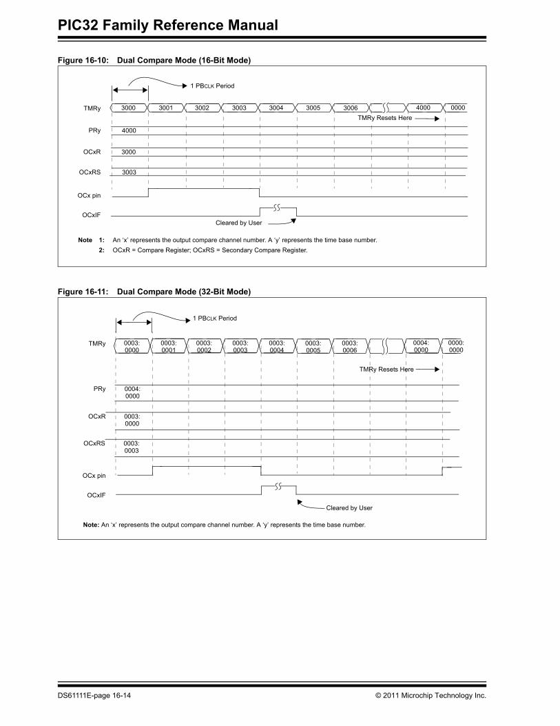
To configure the Output Compare module for the Single Output Pulse mode, set the OCM<2:0> control bits to ‘100’. In addition, the compare time base must be selected and enabled. Once this mode has been enabled, the output pin, OCx, will be driven low and remain low until a match occurs between the time base and OCxR registers. In Figure 16-10 and Figure 16-12, note the following key timing events:
• The OCx pin is driven high one peripheral clock after the compare match occurs between the compare time base and the OCxR register. The OCx pin will remain high until the next match event occurs between the time base and the OCxRS register. At this time, the pin will be driven low. The OCx pin will remain low until a mode change has been made or the module is disabled.
• The compare time base will count up to the value contained in the associated period register, and then reset to 0x0000 on the next instruction clock
• If the time base period register contents are less than the OCxRS register contents, no falling edge of the pulse is generated. The OCx pin will remain high until OCxRS ≤ PR2, or a mode change or Reset condition has occurred.
• The respective channel interrupt flag, OCxIF, is asserted when the OCx pin is driven low (falling edge of single pulse)
Figure 16-10 depicts the General Dual Compare mode generating a single output pulse. Figure 16-12 depicts another timing example where OCxRS > PR2. In this example, no falling edge of the pulse is generated because the compare time base resets before counting up to 0x4100.
© 2011 Microchip Technology Inc. DS61111E-page 16-13
PIC32 Family Reference Manual
Figure 16-10: Dual Compare Mode (16-Bit Mode)
Figure 16-11: Dual Compare Mode (32-Bit Mode)
OCxIF
00003001 3002 3003 30043000TMRy 4000
Cleared by User
Note 1: An ‘x’ represents the output compare channel number. A ‘y’ represents the time base number.2: OCxR = Compare Register; OCxRS = Secondary Compare Register.
1 PBCLK Period
4000
3000
PRy
OCxR
3006
OCx pin
TMRy Resets Here
3003OCxRS
3005
OCxIF
0000:0003: 0003: 0003:0003:0003:TMRy 0004:
1 PBCLK Period
0004:
0003:
PRy
OCxR
0003:
OCx pin
TMRy Resets Here
Note: An ‘x’ represents the output compare channel number. A ‘y’ represents the time base number.
0000
0000 0001 0002 00050004
0000
0006 0000 0000
Cleared by User
0003:0003
0003:OCxRS0003
DS61111E-page 16-14 © 2011 Microchip Technology Inc.

Section 16. Output CompareO
utput Com
pare
16
Figure 16-12: Dual Compare Mode: Single Output Pulse (OCxRS > PRy, 16-Bit Mode)Figure 16-13: Dual Compare Mode: Single Output Pulse (OCxRS > PRy, 32-Bit Mode)
OCxIF
00003001 3002 3003 30043000TMRy 4000
1 PBCLK Period
4000
3000
PRy
OCxR
3006
OCx pin
TMRy Resets Here
4100OCxRS
3005
Note 1: An ‘x’ represents the output compare channel number. A ‘y’ represents the time base number.2: OCxR = Compare Register; OCxRS = Secondary Compare Register.
Compare Interrupt does not occur
OCxIF
0000:0003: 0003: 0003:0003:0003:TMRy 0004:
1 PBCLK Period
0004:
0003:
PRy
OCxR
0003:
OCx pin
TMRy Resets Here
Note: An ‘x’ represents the output compare channel number. A ‘y’ represents the time base number.
0000
0000 0001 0002 00050004
0000
0006 0000 00000003:0003
0004:OCxRS1000
No Compare Interrupt is generated
© 2011 Microchip Technology Inc. DS61111E-page 16-15
PIC32 Family Reference Manual
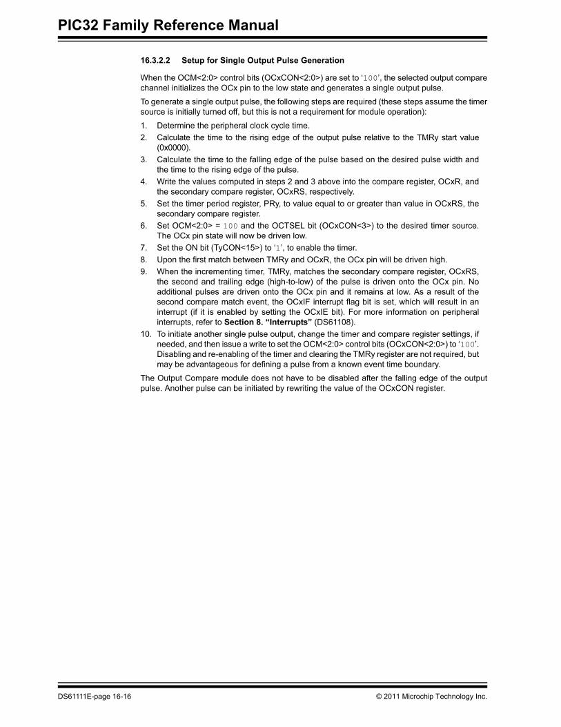
16.3.2.2 Setup for Single Output Pulse Generation
When the OCM<2:0> control bits (OCxCON<2:0>) are set to ‘100’, the selected output compare channel initializes the OCx pin to the low state and generates a single output pulse.
To generate a single output pulse, the following steps are required (these steps assume the timer source is initially turned off, but this is not a requirement for module operation):
1. Determine the peripheral clock cycle time. 2. Calculate the time to the rising edge of the output pulse relative to the TMRy start value
(0x0000).3. Calculate the time to the falling edge of the pulse based on the desired pulse width and
the time to the rising edge of the pulse.4. Write the values computed in steps 2 and 3 above into the compare register, OCxR, and
the secondary compare register, OCxRS, respectively.5. Set the timer period register, PRy, to value equal to or greater than value in OCxRS, the
secondary compare register.6. Set OCM<2:0> = 100 and the OCTSEL bit (OCxCON<3>) to the desired timer source.
The OCx pin state will now be driven low.7. Set the ON bit (TyCON<15>) to ‘1’, to enable the timer.8. Upon the first match between TMRy and OCxR, the OCx pin will be driven high.9. When the incrementing timer, TMRy, matches the secondary compare register, OCxRS,
the second and trailing edge (high-to-low) of the pulse is driven onto the OCx pin. No additional pulses are driven onto the OCx pin and it remains at low. As a result of the second compare match event, the OCxIF interrupt flag bit is set, which will result in an interrupt (if it is enabled by setting the OCxIE bit). For more information on peripheral interrupts, refer to Section 8. “Interrupts” (DS61108).
10. To initiate another single pulse output, change the timer and compare register settings, if needed, and then issue a write to set the OCM<2:0> control bits (OCxCON<2:0>) to ‘100’. Disabling and re-enabling of the timer and clearing the TMRy register are not required, but may be advantageous for defining a pulse from a known event time boundary.
The Output Compare module does not have to be disabled after the falling edge of the output pulse. Another pulse can be initiated by rewriting the value of the OCxCON register.
DS61111E-page 16-16 © 2011 Microchip Technology Inc.

Section 16. Output CompareO
utput Com
pare
16
Examples 16-5 and 16-6 show example code for configuration of the single output pulse event.Example 16-5: Single Output Pulse Setup and Interrupt Servicing (16-Bit Mode)// The following code example will set the Output Compare 1 module // for interrupts on the single pulse event and select Timer2 // as the clock source for the compare time base.
T2CON = 0x0010; // Configure Timer2 for a prescaler of 2
OC1CON = 0x0000; // Turn off OC1 while doing setup. OC1CON = 0x0004; // Configure for single pulse mode OC1R = 0x3000; // Initialize primary Compare Register OC1RS = 0x3003; // Initialize secondary Compare Register PR2 = 0x3003; // Set period (PR2 is now 32-bits wide)
// configure int IFS0CLR = 0x00000040; // Clear the OC1 interrupt flag IFS0SET = 0x00000040; // Enable OC1 interrupt IPC1SET = 0x001C0000; // Set OC1 interrupt priority to 7,
// the highest levelIPC1SET = 0x00030000; // Set Subpriority to 3, maximum
T2CONSET = 0x8000; // Enable Timer2OC1CONSET = 0x8000; // Enable OC1
// Example code for Output Compare 1 ISR:
void__ISR(_OUTPUT_COMPARE_1_VECTOR, ipl7) OC1_IntHandler (void){
// Insert user code hereIFS0CLR = 0x0040; // Clear the OC1 interrupt flag
}
© 2011 Microchip Technology Inc. DS61111E-page 16-17

PIC32 Family Reference Manual
Example 16-6: Single Output Pulse Setup and Interrupt Servicing (32-Bit Mode)// The following code example will set the Output Compare 1 module // for interrupts on the single pulse event and select Timer2 // as the clock source for the compare time base.
T2CON = 0x0018; // Configure Timer2 for 32-bit operation // with a prescaler of 2. The Timer2/Timer3// pair is accessed via registers associated// with the Timer2 register
OC1CON = 0x0000; // Turn off OC1 while doing setup. OC1CON = 0x0004; // Configure for single pulse mode OC1R = 0x00203000; // Initialize primary Compare Register OC1RS = 0x00203003; // Initialize secondary Compare Register PR2 = 0x00500000; // Set period (PR2 is now 32-bits wide)
// configure int IFS0CLR = 0x00000040; // Clear the OC1 interrupt flag IFS0SET = 0x00000040; // Enable OC1 interrupt IPC1SET = 0x001C0000; // Set OC1 interrupt priority to 7, // the highest levelIPC1SET = 0x00030000; // Set Subpriority to 3, maximum
T2CONSET = 0x8000; // Enable Timer2OC1CONSET = 0x8000; // Enable OC1 // Example code for Output Compare 1 ISR:
void__ISR(_OUTPUT_COMPARE_1_VECTOR, ipl7) OC1_IntHandler (void){
// insert user code hereIFS0CLR = 0x0040; // Clear the OC1 interrupt flag
}
DS61111E-page 16-18 © 2011 Microchip Technology Inc.

Section 16. Output CompareO
utput Com
pare
16
16.3.2.3 Special Cases for Dual Compare Mode Generating a Single Output PulseDepending on the relationship of the OCxR, OCxRS and PRy values, the Output Compare module has a few unique conditions that should be understood. These special conditions are specified in Table 16-2, along with the resulting behavior of the module.
Table 16-2: Special Cases for Dual Compare Mode Generating a Single Output Pulse(1)
SFR LogicalRelationship
Special Conditions Operation Output
at OCx
PRy ≥ OCxRS andOCxRS > OCxR
OCxR = 0Initialize TMRy = 0
In the first iteration of the TMRy counting from 0x0000 up to PRy, the OCx pin remains low; no pulse is generated. After the TMRy resets to zero (on period match), the OCx pin goes high due to a match with OCxR. Upon the next TMRy to OCxRS match, the OCx pin goes low and remains there. The OCxIF bit will be set as a result of the second compare.There are two alternative initial conditions to consider:1. Initialize TMRy = 0 and set OCxR ≥ 1.2. Initialize TMRy = PRy (PRy > 0) and set OCxR = 0.
Pulse will be delayed by the value in the PRy register, depending on setup
PRy ≥ OCxR andOCxR ≥ OCxRS
OCxR ≥ 1 andPRy ≥ 1
TMRy counts up to OCxR and on a compare match event (i.e., TMRy = OCxR), the OCx pin is driven to a high state. TMRy then continues to count and eventually resets on a period match (i.e., PRy = TMRy). The timer then restarts from 0x0000 and counts up to OCxRS. On a compare match event (i.e., TMRy = OCxRS), the OCx pin is driven to a low state. The OCxIF bit will be set as a result of the second compare.
Pulse
OCxRS > PRy andPRy ≥ OCxR
None Only the rising edge will be generated at the OCx pin. The OCxIF will not be set.
Rising edge/transition to high
OCxR > PRy None Unsupported mode; timer resets prior to match condition. Remains lowLegend: OCxR = Compare Register OCxRS = Secondary Compare Register TMRy = Timery Count
PRy = Timery Period RegisterNote 1: In all of these cases, the TMRy register is assumed to be initialized to 0x0000.
© 2011 Microchip Technology Inc. DS61111E-page 16-19

PIC32 Family Reference Manual
16.3.2.4 Dual Compare Mode: Continuous Output PulsesTo configure the Output Compare module for this mode, set the OCM<2:0> control bits to ‘101’.In addition, the compare time base must be selected and enabled. Once this mode has been enabled, the output pin, OCx, will be driven low and remain low until a match occurs between the compare time base and OCxR register. In Figure 16-14 and Figure 16-16, note the following key timing events:
• The OCx pin is driven high one PBCLK after the compare match occurs between the compare time base and OCxR register. The OCx pin will remain high until the next match event occurs between the time base and the OCxRS register, at which time the pin will be driven low. This pulse generation sequence of a low-to-high and high-to-low edge will repeat on the OCx pin without further user intervention.
• Continuous pulses will be generated on the OCx pin until a mode change is made or the module is disabled
• The compare time base will count up to the value contained in the associated period register, and then reset to 0x0000 on the next instruction clock
• If the compare time base period register value is less than the OCxRS register value, no falling edge is generated. The OCx pin will remain high until OCxRS ≤ PRy, a mode change is made, or the device is Reset.
• The respective channel interrupt flag, OCxIF, is asserted when the OCx pin is driven low (falling edge of single pulse)
General Dual Compare mode generating a continuous output pulse is illustrated in Figure 16-14. Figure 16-16 depicts another timing example where OCxRS > PRy. In this example, no falling edge of the pulse is generated, because the time base will reset before counting up to the contents of OCxRS.
Figure 16-14: Dual Compare Mode: Continuous Output Pulse (PRy = OCxRS, 16-Bit Mode)
Note 1: An ‘x’ represents the output compare channel number. A ‘y’ represents the time base number.
2: OCxR = Compare Register; OCxRS = Secondary Compare Register.
OCxIF
00003001 3002 0000 00013000TMRy 3002
Cleared by User
1 PBCLK Period
3002
3000
PRy
OCxR
3000
OCx pin
3002OCxRS
3001 30000001
TMRy Resets Here due to PRx match TMRy Resets Here ...
Cleared by User
DS61111E-page 16-20 © 2011 Microchip Technology Inc.

Section 16. Output CompareO
utput Com
pare
16
Figure 16-15: Dual Compare Mode: Continuous Output Pulse (PRy = OCxRS, 32-Bit Mode)Figure 16-16: Dual Compare Mode: Continuous Output Pulse (PRy = OCxRS, 16-Bit Mode)
OCxIF
0000:0003: 0000:0003:TMRy 0000:
1 PBCLK Period
0003:
0003:
PRy
OCxR
0003:
OCx pin
TMRy Resets Here
Note: An ‘x’ represents the output compare channel number. A ‘y’ represents the time base number.
0000
0000 0001 0000
0001
0001 0001 0002
Cleared by User
0000:0001
0003:OCxRS0001
0000:0000
0003:0000
TMRy Resets Here
Cleared by User
OCxIF
30033001 3002 3003 00003000TMRy 3002
1 PBCLK Period
3003
3000
PRy
OCxR
3000
OCx pin
3003OCxRS
3001 30000000
TMRy Resets Here TMRy Resets Here
Note 1: An ‘x’ represents the output compare channel number. A ‘y’ represents the time base number.2: OCxR = Compare Register; OCxRS = Secondary Compare Register.
Cleared by User Cleared by User
© 2011 Microchip Technology Inc. DS61111E-page 16-21

PIC32 Family Reference Manual
16.3.2.5 Setup for Continuous Output Pulse Generation
When the OCM<2:0> control bits are set to ‘101’, the selected output compare channel initializes the OCx pin to the low state and generates output pulses on each and every compare match event.
For the user to configure the module for the generation of a continuous stream of output pulses, the following steps are required (these steps assume the timer source is initially turned off, but this is not a requirement for the module operation):
1. Determine the peripheral clock cycle time. Take into account the frequency of the external clock to the timer source (if one is used) and the timer prescaler settings.
2. Calculate the time to the rising edge of the output pulse, relative to the TMRy start value (0x0000).
3. Calculate the time to the falling edge of the pulse, based on the desired pulse width and the time to the rising edge of the pulse.
4. Write the values computed in step 2 and 3 above into the compare register, OCxR, and the secondary compare register, OCxRS, respectively.
5. Set the timer period register, PRy, to a value equal to or greater than the value in OCxRS, the secondary compare register.
6. Set OCM<2:0> = 101 and the OCTSEL bit (OCxCON<3>) to the desired timer source (for 16-bit mode only). The OCx pin state will now be driven low.
7. Enable the compare time base by setting the TON bit (TyCON<15>) to ‘1’. 8. Upon the first match between TMRy and OCxR, the OCx pin will be driven high.9. When the compare time base, TMRy, matches the secondary compare register, OCxRS,
the second and trailing edge (high-to-low) of the pulse is driven onto the OCx pin.10. As a result of the second compare match event, the OCxIF interrupt flag bit is set.11. When the compare time base and the value in its respective period register match, the
TMRy register resets to 0x0000 and resumes counting.12. Steps 8 through 11 are repeated, and a continuous stream of pulses is generated,
indefinitely. The OCxIF flag (refer to the IFS0 register for the bit position of each channel’s interrupt flag) is set on each OCxRS-TMRy compare match event.
DS61111E-page 16-22 © 2011 Microchip Technology Inc.
Section 16. Output CompareO
utput Com
pare
16
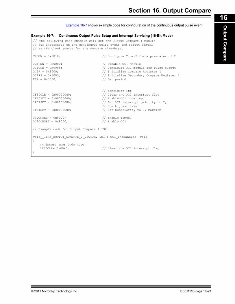
Example 16-7 shows example code for configuration of the continuous output pulse event.Example 16-7: Continuous Output Pulse Setup and Interrupt Servicing (16-Bit Mode)// The following code example will set the Output Compare 1 module // for interrupts on the continuous pulse event and select Timer2 // as the clock source for the compare time-base.
T2CON = 0x0010; // Configure Timer2 for a prescaler of 2
OC1CON = 0x0000; // Disable OC1 moduleOC1CON = 0x0005; // Configure OC1 module for Pulse outputOC1R = 0x3000; // Initialize Compare Register 1OC1RS = 0x3003; // Initialize Secondary Compare Register 1 PR2 = 0x5000; // Set period
// configure int IFS0CLR = 0x00000040; // Clear the OC1 interrupt flag IFS0SET = 0x00000040; // Enable OC1 interrupt IPC1SET = 0x001C0000; // Set OC1 interrupt priority to 7, // the highest levelIPC1SET = 0x00030000; // Set Subpriority to 3, maximum
T2CONSET = 0x8000; // Enable Timer2OC1CONSET = 0x8000; // Enable OC1 // Example code for Output Compare 1 ISR:
void__ISR(_OUTPUT_COMPARE_1_VECTOR, ipl7) OC1_IntHandler (void){
// insert user code hereIFS0CLR= 0x0040; // Clear the OC1 interrupt flag
}
© 2011 Microchip Technology Inc. DS61111E-page 16-23

PIC32 Family Reference Manual
Example 16-8: Continuous Output Pulse Setup and Interrupt Servicing (32-Bit Mode)// The following code example will set the Output Compare 1 module // for interrupts on the continuous pulse event and select Timer2 // as the clock source for the compare time-base.
T2CON = 0x0018; // Configure Timer2 for 32-bit operation // with a prescaler of 2. The Timer2/Timer3// pair is accessed via registers associated// with the Timer2 register
OC1CON = 0x0000; // disable OC1 moduleOC1CON = 0x0005; // Configure OC1 module for Pulse outputOC1R = 0x3000; // Initialize Compare Register 1OC1RS = 0x3003; // Initialize Secondary Compare Register 1 PR2 = 0x00500000; // Set period (PR2 is now 32-bits wide)
// configure int
IFS0CLR = 0x00000040; // Clear the OC1 interrupt flag IFS0SET = 0x00000040; // Enable OC1 interrupt IPC1SET = 0x001C0000; // Set OC1 interrupt priority to 7, // the highest levelIPC1SET = 0x00030000; // Set Subpriority to 3, maximum
T2CONSET = 0x8000; // Enable Timer2OC1CONSET = 0x8000; // Enable OC1 // Example code for Output Compare 1 ISR:
void__ISR(_OUTPUT_COMPARE_1_VECTOR, ipl7) OC1_IntHandler (void){
// insert user code hereIFS0CLR = 0x0040; // Clear the OC1 interrupt flag
}
DS61111E-page 16-24 © 2011 Microchip Technology Inc.

Section 16. Output CompareO
utput Com
pare
16
16.3.2.6 Special Cases for Dual Compare Mode Generating Continuous Output PulsesDepending on the relationship of the OCxR, OCxRS and PRy values, the Output Compare module may not provide the expected results. These special cases are specified in Table 16-3, along with the resulting behavior of the module.
Table 16-3: Special Cases for Dual Compare Mode Generating Continuous Output Pulses(1)
SFR LogicalRelationship
Special Conditions Operation Output
at OCx
PRy ≥ OCxRS andOCxRS > OCxR
OCxR = 0Initialize TMRy = 0
In the first iteration of the TMRy counting from 0x0000 up to PRy, the OCx pin remains low; no pulse is generated. After the TMRy resets to zero (on period match), the OCx pin goes high. Upon the next TMRy to OCxRS match, the OCx pin goes low. If OCxR = 0 and PRy = OCxRS, the pin will remain low for one clock cycle, then be driven high until the next TMRy to OCxRS match. The OCxIF bit will be set as a result of the second compare.There are two alternative initial conditions to consider:1. Initialize TMRy = 0 and set OCxR ≥ 1.2. Initialize TMRy = PRy (PRy > 0) and set
OCxR = 0.
Continuous pulses with the first pulse delayed by the value in the PRy register, depending on setup.
PRy ≥ OCxR andOCxR ≥ OCxRS
OCxR ≥ 1 andPRy ≥ 1
TMRy counts up to OCxR and on a compare match event (i.e., TMRy = OCxR), the OCx pin is driven to a high state. TMRy then continues to count and eventually resets on period match (i.e., PRy = TMRy). The timer then restarts from 0x0000 and counts up to OCxRS. On a compare match event (i.e., TMRy = OCxR), the OCx pin is driven to a low state. The OCxIF bit will be set as a result of the second compare.
Continuous pulses
OCxRS > PRy andPRy ≥ OCxR
None Only one transition will be generated at the OCx pin until the OCxRS register contents have been changed to a value less than or equal to the period register contents (PRy). OCxIF is not set until then.
Rising edge/ transition to high
OCxR > PRy None Unsupported mode; Timer resets prior to match condition.
Remains low
Legend: OCxR = Compare Register OCxRS = Secondary Compare Register TMRy = Timery Count PRy = Timery Period Register
Note 1: In all of these cases, the TMRy register is assumed to be initialized to 0x0000.
© 2011 Microchip Technology Inc. DS61111E-page 16-25

PIC32 Family Reference Manual
16.3.3 Pulse Width Modulation ModeWhen the OCM<2:0> control bits are set to ‘110’ or ‘111’, the selected output compare channel is configured for the PWM mode of operation.
The following two PWM modes are available:
• PWM without Fault Protection Input• PWM with Fault Protection Input
The OCFA or OCFB Fault input pin is utilized for the second PWM mode. In this mode, an asynchronous logic level ‘0’ on the OCFx pin will cause the selected PWM channel to be shut down. See 16.3.3.1 “PWM with Fault Protection Input Pin”.
In PWM mode, the OCxR register is a read-only slave duty cycle register and OCxRS is a buffer register that is written by the user to update the PWM duty cycle. On every timer to period register match event (end of PWM period), the duty cycle register, OCxR, is loaded with the contents of OCxRS. The TyIF interrupt flag is asserted at each PWM period boundary.
The following steps should be taken when configuring the Output Compare module for PWM operation:
1. Set the PWM period by writing to the selected timer period register (PRy).2. Set the PWM duty cycle by writing to the OCxRS register.3. Write the OxCR register with the initial duty cycle.4. Enable interrupts, if required, for the timer and Output Compare modules. The output
compare interrupt is required for PWM Fault pin utilization.5. Configure the Output Compare module for one of two PWM Operation modes by writing
to the Output Compare mode bits, OCM<2:0> (OCxCON<2:0>).6. Set the TMRy prescale value and enable the time base by setting TON (TxCON<15>) = 1.
An example PWM output waveform is shown in Figure 16-17.
Figure 16-17: PWM Output Waveform
Note: The OCxR register should be initialized before the Output Compare module is first enabled. The OCxR register becomes a read-only duty cycle register when the module is operated in the PWM modes. The value held in OCxR will become the PWM duty cycle for the first PWM period. The contents of the duty cycle buffer register, OCxRS, will not be transferred into OCxR until a time base period match occurs.
Period = (PRy + 1)
Duty Cycle = (OCxRS)
Timery is cleared and the new duty cycle value is loaded from OCxRS into OCxR.
Timer value equals the value in the OCxR register; OCx Pin is driven low.
Timer overflow; value from OCxRS is loaded into OCxR; OCx pin is driven high.
21 3
2
3
1
TyIF interrupt flag is asserted.
DS61111E-page 16-26 © 2011 Microchip Technology Inc.

Section 16. Output CompareO
utput Com
pare
16
16.3.3.1 PWM with Fault Protection Input PinWhen the OCM<2:0> control bits are set to ‘111’, the selected output compare channel is configured for the PWM mode of operation. All functions described in 16.3.3 “Pulse Width Modulation Mode” apply, with the addition of input Fault protection.
Fault protection is provided via the OCFA and OCFB pins. The OCFA pin is associated with the output compare channels 1 through 4, while the OCFB pin is associated with the output compare channel 5.
If a logic ‘0’ is detected on the OCFA/OCFB pin, the selected PWM output pin(s) are placed in the tri-state. The user may elect to provide a pull-down or pull-up resistor on the PWM pin to provide for a desired state if a Fault condition occurs. The shutdown of the PWM output is immediate and is not tied to the device clock source. This state will remain until the following conditions are met:
• The external Fault condition has been removed• The PWM mode is re-enabled by writing to the appropriate mode bits, OCM<2:0> bits
(OCxCON<2:0>)
As a result of the Fault condition, the respective interrupt flag, OCxIF bit, is asserted and an interrupt will be generated, if enabled. Upon detection of the Fault condition, the OCFLT bit (OCxCON<4>) is asserted high (logic ‘1’). This bit is a read-only bit and will only be cleared once the external Fault condition has been removed and the PWM mode is re-enabled by writing to the appropriate mode bits, OCM<2:0> (OCxCON<2:0>).
16.3.3.2 PWM Period
The PWM period is specified by writing to the Timery Period register, PRy. The PWM period can be calculated using the following formula:
Equation 16-1: Calculating the PWM Period
The PWM period must not exceed the width of the Period Register for the selected mode, 16 bits for 16-bit mode or 32 bits for 32-bit mode. If the calculated period is too large, select a larger prescaler to prevent overflow. To maintain maximum PWM resolution, select the smallest prescaler that does not result in an overflow.
Note: The external Fault pins, if enabled for use, will continue to control the OCx output pins while the device is in Sleep or Idle mode.
PWM Period = [(PR + 1) • TPB • (TMR Prescale Value)]
PWM Frequency = 1/[PWM Period]
Note: A PRy value of N will produce a PWM period of N + 1 time base count cycles. For example, a value of 7 written into the PRy register will yield a period consisting of 8 time base cycles.
© 2011 Microchip Technology Inc. DS61111E-page 16-27

PIC32 Family Reference Manual
16.3.3.3 PWM Duty Cycle
The PWM duty cycle is specified by writing to the OCxRS register. The OCxRS register can be written to at any time, but the duty cycle value is not latched into OCxR until a match between PRy and TMRy occurs (i.e., the period is complete). This provides a double buffer for the PWM duty cycle and is essential for glitchless PWM operation. In the PWM mode, OCxR is a read-only register.
Some important boundary parameters of the PWM duty cycle include the following:
• If the duty cycle register OCxR is loaded with 0x0000, the OCx pin will remain low (0% duty cycle)
• If OCxR is greater than PRy (timer period register), the pin will remain high (100% duty cycle)• If OCxR is equal to PRy, the OCx pin will be low for one time base count value and high for
all other count values
See Figure 16-18 for PWM mode timing details. Table 16-4 through Table 16-9 show example PWM frequencies and resolutions for a device with the Peripheral Bus operating at a variety of frequencies.
Equation 16-2: Calculation for Maximum PWM Resolution
Equation 16-3: PWM Period and Resolution Calculation
( )Maximum PWM Resolution (bits) =
FPBFPWM • TMRy • Prescaler bits
log10
log10(2)
Desired PWM frequency is 52.08 kHz FPB = 10 MHz
Timer2 prescale setting: 1:1
1/52.08 kHz = (PR2 + 1) • TPB • (Timer2 prescale value) 19.20 μs = (PR2 + 1) • 0.1 μs • (1)
PR2 = 191
Find the maximum resolution of the duty cycle that can be used with a 52.08 kHz PWM frequency and a 10 MHz Peripheral Bus clock rate.
1/52.08 kHz = 2PWM RESOLUTION • 1/10 MHz • 1 19.20 μs = 2PWM RESOLUTION • 100 ns • 1
192 = 2PWM RESOLUTION log10(192) = (PWM Resolution) • log10(2)
PWM Resolution = 7.6 bits
DS61111E-page 16-28 © 2011 Microchip Technology Inc.

Section 16. Output CompareO
utput Com
pare
16
Figure 16-18: PWM Output TimingFigure 16-19: Dual Compare Mode: Continuous Output Pulse (PR2 = OCxRS, 32-Bit Mode)
00020000 0001 0002 00030005TMR3 0001
1 PBCLK Period
0005
0002
PR3
OCxR
0005
OCx pin
0002OCxRS
0000 000500030004 0004
0001
User Code Writes New Value to OCxRS In ISR
0001
Hardware Loads New Duty Cycle Here
Note 1: An ‘x’ represents the output compare channel number.2: OCxR = Compare Register; OCxRS = Secondary Compare Register.
T3IF is SetOCxR = OCxRS T3IF is Set
OCxR = OCxRS
0000:0000: 0000: 0000:0000:0005:TMR2 0000:
1 PBCLK Period
0000:
0000:
PR2
OCxR
0000:
OCx pin
Hardware Loads New Duty Cycle Here
Note: An ‘x’ represents the output compare channel number.
0002
0000 0000 0001 00040003
0005
0005 0001 00020000:0002
0000:OCxRS0002
0000:0000
0000:0001
0000:0001
User Code Writes New Value to OCxRS in ISR
© 2011 Microchip Technology Inc. DS61111E-page 16-29

PIC32 Family Reference Manual
Table 16-4: Example PWM Frequencies and Resolutions with a 10 MHz (16-Bit Mode) Peripheral Bus ClockPWM Frequency 19 Hz 153 Hz 305 Hz 2.44 kHz 9.77 kHz 78.1 kHz 313 kHz
Timer Prescaler Ratio 8 1 1 1 1 1 1Period Register Value 0xFFFF 0xFFFF 0x7FFF 0x0FFF 0x03FF 0x007F 0x001FResolution (bits) 16 16 15 12 10 7 5
Table 16-5: Example PWM Frequencies and Resolutions with a 30 MHz (16-Bit Mode) Peripheral Bus ClockPWM Frequency 58 Hz 458 Hz 916 Hz 7.32 kHz 29.3 kHz 234 kHz 938 kHz
Timer Prescaler Ratio 8 1 1 1 1 1 1Period Register Value 0xFC8E 0xFFDD 0x7FEE 0x1001 0x03FE 0x007F 0x001EResolution (bits) 16 16 15 12 10 7 5
Table 16-6: Example PWM Frequencies and Resolutions with a 50 MHz (16-Bit Mode) Peripheral Bus ClockPWM Frequency 57 Hz 458 Hz 916 Hz 7.32 kHz 29.3 kHz 234 kHz 938 kHz
Timer Prescaler Ratio 64 8 1 1 1 1 1Period Register Value 0x349C 0x354D 0xD538 0x1AAD 0x06A9 0x00D4 0x0034Resolution (bits) 13.7 13.7 15.7 12.7 10.7 7.7 5.7
Table 16-7: Example PWM Frequencies and Resolutions with a 50 MHz (16-Bit Mode) Peripheral Bus ClockPWM Frequency 100 Hz 200 Hz 500 Hz 1 kHz 2 kHz 5 kHz 10 kHz
Timer Prescaler Ratio
8 8 8 1 8 1 1
Period Register Value (hex)
0xF423 0x7A11 0x30D3 0xC34F 0x0C34 0x270F 0x1387
Resolution (bits) (decimal)
15.9 14.9 13.6 15.6 11.6 13.3 12.3
Table 16-8: Example PWM Frequencies and Resolutions with a 50 MHz (16-Bit Mode) Peripheral Bus ClockPWM Frequency 100 Hz 200 Hz 500 Hz 1 kHz 2 kHz 5 kHz 10 kHz
Timer Prescaler Ratio
8 4 2 1 1 1 1
Period Register Value (hex)
0xF423 0xF423 0xC34F 0x0C34F 0x61A7 0x270F 0x1387
Resolution (bits) (decimal)
15.9 15.9 15.6 15.6 14.6 13.3 12.3
Table 16-9: Example PWM Frequencies and Resolutions with a 50 MHz (32-Bit Mode) Peripheral Bus ClockPWM
Frequency 100 Hz 200 Hz 500 Hz 1 kHz 2 kHz 5 kHz 10 kHz
Timer Prescaler Ratio
1 1 1 1 1 8 1
Period Register Value (hex)
0x0007A11F 0x0003D08F 0x0001869F 0x0000C34F 0x000061A7 0x000004E1 0x00001387
Resolution (bits) (decimal)
18.9 17.9 16.6 15.6 14.6 10.3 12.3
DS61111E-page 16-30 © 2011 Microchip Technology Inc.
Section 16. Output CompareO
utput Com
pare
16
Example 16-9 shows configuration and interrupt service code for the PWM mode of operation.Example 16-9: PWM Mode Setup and Interrupt Servicing (16-Bit Mode)// The following code example will set the Output Compare 1 module // for PWM mode with Fault pin disabled and for 50% duty cycle. // Timer2 is selected as the clock for the PWM time base, and Timer2 // interrupts are enabled.
#include <plib.h>
int main(void){
INTEnableSystemMultiVectoredInt(); // Enable system wide interrupt to // multivectored mode.
OC1CON = 0x0000; // Turn off the OC1 when performing the setupOC1R = 0x0064; // Initialize primary Compare registerOC1RS = 0x0064; // Initialize secondary Compare registerOC1CON = 0x0006; // Configure for PWM mode without Fault pin
// enabledPR2 = 0x00C7; // Set period
// Configure Timer2 interrupt. Note that in PWM mode, the // corresponding source timer interrupt flag is asserted.// OC interrupt is not generated in PWM mode.
IFS0CLR = 0x00000100; // Clear the T2 interrupt flagIEC0SET = 0x00000100; // Enable T2 interruptIPC2SET = 0x0000001C; // Set T2 interrupt priority to 7
T2CONSET = 0x8000; // Enable Timer2OC1CONSET = 0x8000; // Enable OC1
while(1); // Never return}
// Example code for Timer2 ISR
void __ISR(_TIMER_2_VECTOR, ipl7) T2_IntHandler (void){
// Insert user code hereIFS0CLR = 0x0100; // Clearing Timer2 interrupt flag
}
© 2011 Microchip Technology Inc. DS61111E-page 16-31

PIC32 Family Reference Manual
Example 16-10: PWM Mode Setup and Interrupt Servicing (32-Bit Mode)// The following code example will set the Output Compare 1 module // for PWM mode with Fault pin disabled and for 50% duty cycle. // Timer2 and Timer3 are selected as the clocks for the PWM time base // in 32-bit mode, and Timer3 interrupts are enabled.
#include <plib.h>
int main(void){
INTEnableSystemMultiVectoredInt(); // Enable system wide interrupt to multivectored mode.
OC1CON = 0x0000; // Turn off the OC1 when performing the setupOC1R = 0x00638000; // Initialize primary Compare registerOC1RS = 0x00638000; // Initialize secondary Compare registerOC1CON = 0x0006; // Configure for PWM mode without Fault pin enabledT2CONSET = 0x0008; // Enable 32-bit Timer modePR2 = 0x00C6FFFF; // Set period
// Configure Timer3 interrupt. Note that in PWM mode, the corresponding source timer // interrupt flag is asserted. OC interrupt is not generated in PWM mode.
IFS0CLR = 0x00001000; // Clear the T3 interrupt flagIEC0SET = 0x00001000; // Enable T3 interruptIPC3SET = 0x0000001C; // Set T3 interrupt priority to 7
T2CONSET = 0x8000; // Enable Timer2OC1CONSET = 0x8020; // Enable OC1 in 32-bit mode.
while(1); // Never return}
// Example code for Timer3 ISR:
void __ISR(_TIMER_3_VECTOR, ipl7) T3_IntHandler (void){
// Insert user code hereIFS0CLR = 0x1000; // Clearing Timer3 interrupt flag
}
DS61111E-page 16-32 © 2011 Microchip Technology Inc.

Section 16. Output CompareO
utput Com
pare
16
16.4 INTERRUPTSEach of the available output compare channels has a dedicated interrupt bit, OCxIF, and a corresponding interrupt enable/mask bit, OCxIE. These bits are used to determine the source of an interrupt and to enable or disable an individual interrupt source. The priority level of each of the channels can also be set independently of the other channels.
OCxIF is set when an output compare channel detects a predefined match condition that is defined as an event generating an interrupt. The OCxIF bit will then be set without regard to the state of the corresponding OCxIE bit. The OCxIF bit can be polled by software if desired.
The OCxIE bit is used to define the behavior of the Vector Interrupt Controller (VIC) when a corresponding OCxIF is set. When the OCxIE bit is clear, the VIC module does not generate a CPU interrupt for the event. If the OCxIE bit is set, the VIC module will generate an interrupt to the CPU when the corresponding OCxIF bit is set (subject to the priority and subpriority as outlined below).
It is the responsibility of the routine that services a particular interrupt to clear the appropriate interrupt flag bit before the service routine is complete.
The priority of each output compare channel can be set independently via the OCxIP<2:0> bits. This priority defines the priority group that the interrupt source will be assigned to. The priority groups range from a value of 7, the highest priority, to a value of 0, which does not generate an interrupt. An interrupt being serviced will be preempted by an interrupt in a higher priority group.
The subpriority bits allow setting the priority of an interrupt source within a priority group. The values of the subpriority, OCxIS<1:0>, range from 3, the highest priority, to 0, the lowest priority. An interrupt with the same priority group but having a higher subpriority value will preempt a lower subpriority interrupt that is in progress.
The priority group and subpriority bits allow more than one interrupt source to share the same priority and subpriority. If simultaneous interrupts occur in this configuration, the natural order of the interrupt sources within a priority/subpriority group pair determines the interrupt generated. The natural priority is based on the vector numbers of the interrupt sources. The lower the vector number, the higher the natural priority of the interrupt. any interrupts that were overridden by natural order will then generate their respective interrupts (based on priority, subpriority, and natural order) after the interrupt flag for the current interrupt is cleared.
After an enabled interrupt is generated, the CPU will jump to the vector assigned to that interrupt. The vector number for the interrupt is the same as the natural order number. The CPU will then begin executing code at the vector address. The user’s code at this vector address should perform any operations required (such as reloading the duty cycle and clearing the interrupt flag), and then exit. For the vector address table details and for more information on interrupts, refer toSection 8. “Interrupts” (DS61108).
© 2011 Microchip Technology Inc. DS61111E-page 16-33

PIC32 Family Reference Manual
16.5 I/O PIN CONTROLWhen the Output Compare module is enabled, it controls the I/O pin direction. The Output Com-pare module returns the I/O pin control back to the appropriate pin LAT and TRIS control bits when it is disabled.
When the PWM with Fault Protection Input mode is enabled, the OCFx Fault pin must be configured for an input by setting the respective TRIS SFR bit. The OCFx Fault input pin is not automatically configured as an input when the PWM fault mode is selected.
Table 16-10: Pins Associated with Output Compare Modules 1-5Pin
NameModule Control
PinType
BufferType Description
OC1 ON O — Output Compare/PWM Channel 1OC2 ON O — Output Compare/PWM Channel 2OC3 ON O — Output Compare/PWM Channel 3OC4 ON O — Output Compare/PWM Channel 4OC5 ON O — Output Compare/PWM Channel 5
OCFA ON I ST PWM Fault Protection A Input (for Channels 1-4)OCFB ON I ST PWM Fault Protection B Input (for Channel 5)
Legend: ST = Schmitt Trigger input with CMOS levels I = Input O = Output
DS61111E-page 16-34 © 2011 Microchip Technology Inc.

Section 16. Output CompareO
utput Com
pare
16
16.6 OPERATION IN POWER-SAVING AND DEBUG MODES16.6.1 Output Compare Operation in Sleep ModeWhen the device enters Sleep mode, the system clock is disabled. During Sleep, the Output Compare module drives the pin to the same active state as driven prior to entering Sleep. The module will then halt at this state.
For example, if the pin was high and the CPU entered the Sleep state, the pin will stay high. Likewise, if the pin was low and the CPU entered the Sleep state, the pin will stay low. In both cases, when the device wakes up, the Output Compare module will resume operation.
When the module is operating in PWM Fault mode, the asynchronous portions of the Fault circuit remain active. If a Fault is detected, the compare output enable signal is deasserted and the OCFLT bit (OCxCON<4>) is set. If the corresponding interrupt is enabled, an interrupt is generated and the device wakes up from Sleep.
16.6.2 Output Compare Operation in Idle ModeWhen the device enters Idle mode, the system clock sources remain functional and the CPU stops executing code. The SIDL bit (OCxCON<13>) selects if the Output Compare module will stop operation when the device enters Idle mode or whether the module will continue normal operation in Idle mode.
• If SIDL = 1, the module will discontinue operation in Idle mode. The module will perform the same procedures when stopped in Idle mode as it does for Sleep mode.
• If SIDL = 0, the module will continue operation in Idle mode only if the selected time base is set to operate in Idle mode. The output compare channel(s) will operate during Idle mode if the SIDL bit is a logic ‘0’. Furthermore, the time base must be enabled with the respective SIDL bit set to a logic ‘0’.
• When the module is operating in PWM Fault mode, the asynchronous portions of the Fault circuit remain active. If a Fault is detected, the compare output enable signal is deasserted and the OCFLT bit (OCxCON<4>) is set. If the corresponding interrupt is enabled, an interrupt is generated and the device wakes up from Idle.
16.6.3 Output Compare Operation in Debug ModeWhen the module is operating in PWM Fault mode, the asynchronous portions of the Fault circuit remain active. If a Fault is detected, the compare output enable signal is deasserted and the OCFLT bit (OCxCON<4>) is set. If the corresponding interrupt is enabled, an interrupt will be generated.
16.7 EFFECTS OF VARIOUS RESETS
16.7.1 MCLR ResetFollowing a MCLR event, the OCxCON, OCxR, and OCxRS registers for each Output Compare module are reset to a value of 0x00000000.
16.7.2 Power-on ResetFollowing a Power-on (POR) event, the OCxCON, OCxR, and OCxRS registers for each Output Compare module are reset to a value of 0x00000000.
16.7.3 Watchdog Timer ResetThe status of the Output Compare control registers after a Watchdog Timer (WDT) event depends on the operational mode of the CPU prior to the WDT event.
If the device is not in Sleep, a WDT event will force the OCxCON, OCxR, and OCxRS registers to a Reset value of 0x00000000. If the device is in Sleep when a WDT event occurs, the contents of the OCxCON, OCxR and OCxRS register values are not affected.
Note: The external Fault pins, if enabled for use, will continue to control the associated OCx output pins while the device is in Sleep or Idle mode.
© 2011 Microchip Technology Inc. DS61111E-page 16-35
PIC32 Family Reference Manual
16.8 OUTPUT COMPARE APPLICATIONThis section provides an example application using the PWM mode of the Output Compare module to control the speed of a DC motor. The speed of the motor is controlled by changing the PWM duty cycle.
The circuit consists of the following:
• A PIC32 family device to generate the PWM • A TC4431 or equivalent MOSFET driver to drive the MOSFET • A MOSFET to drive the motor • A pull-up resistor is used to pull the input of the MOSFET driver high when the PIC32 family
is in Reset. This prevents unwanted motor operation during start-up. • A DC motor
Example 16-11: PWM Mode Example Application (16-Bit Mode)// The following code example will set the Output Compare 1 module for PWM mode without Fault// pin disabled and for 50% duty cycle. Timer2 is selected as the clock for the PWM time base// and Timer2 interrupts are enabled. This example ramps the PWM duty cycle from min to max,// and then from max to min and repeats. The rate at which the PWM duty cycle is changed can be// adjusted by the rate at which the Timer2 overflows. The PWM period can be changed by writing// a different value to the PR2 register. If the PR2 value is adjusted, the maximum PWM value// will also have to be adjusted so that it is not greater than the PR2 value.
unsigned int Pwm; // Variable to store calculated PWM valueunsigned char Mode = 0; // Variable to determine ramp up or ramp down
OC1CON = 0x0000; // Turn off the OC1 when performing the setupOC1R = 0x0064; // Initialize primary Compare registerOC1RS = 0x0064; // Initialize secondary Compare registerOC1CON = 0x0006; // Configure for PWM mode without Fault pin enabledPR2 = 0x00C7; // Set period
IFS0CLR = 0x00000100; // Clear the T2 interrupt flagIEC0SET = 0x00000100; // Enable T2 interruptIPC2SET = 0x0000001C; // Set T2 interrupt priority to 7
T2CONSET = 0x8000; // Enable Timer2OC1CONSET = 0x8000; // Enable OC1
// Example code for Timer2 ISR:
void __ISR(_TIMER_2_VECTOR, ipl7) T2_IntHandler (void){if ( Mode )
{if ( Pwm < 0xFFFF ) // Ramp up mode{
Pwm ++; // If the duty cycle is not at max, increase OC1RS = Pwm; // Write new duty cycle
}else{
Mode = 0; // PWM is at max, change mode to ramp down}
} // End of ramp upelse{
if ( !Pwm ) // Ramp Down mode{
Pwm --; // If the duty cycle is not at min, increaseOC1RS = Pwm; // Write new duty cycle
}else{
Mode = 1; // PWM is at min, change mode to ramp up}
} // End of ramp down
// Insert user code hereIFS0CLR = 0x0100; // Clearing Timer2 interrupt flag
}
DS61111E-page 16-36 © 2011 Microchip Technology Inc.

Section 16. Output CompareO
utput Com
pare
16
Figure 16-20: DC Motor Speed Control Application SchematicVDD
VDD
VDD
VDD
C81 µF
VDD
C70.1 µF
VDD
C60.01 µF
VDD
C51 µF
VDD
C40.1 µF
VDD
C30.01 µF
M
TC4432
12 V
12 V
VDD
1K9294 93 91 90 89 88 87 86 85 84 83 82 81 80 79 7820
2345678910111213141516
65646362616059
564544434241403928 29 30 31 32 33 34 35 36 37 38
171819
2122
95
1
7677
72717069686766
757473
5857
2423
25
9698 979927 46 47 48 49
5554535251
100
5026
VDD
VDD
VDD
10K
AVDDAVSS
VDD10 µF
© 2011 Microchip Technology Inc. DS61111E-page 16-37

PIC32 Family Reference Manual
16.9 DESIGN TIPS
Question 1: The Output Compare pin stops functioning even when the SIDL bit is not set. Why?
Answer: This is most likely to occur when the SIDL bit (TxCON<13>) of the associated timer source is set. Therefore, it is the timer that actually goes into Idle mode when the PWRSAV instruction is executed.
Question 2: Can I use the Output Compare modules with the selected time base configured for 32-bit mode?
Answer: Yes. The timer can be used in 32-bit mode as a time base for the Output Compare modules by setting the T32 bit (TxCON<3>). For proper operation, the Output Compare module must be configured for 32-bit Compare mode by setting the OC32 bit (OCxCON<5>) for all Output Compare modules using the 32-bit timer as a time base.
DS61111E-page 16-38 © 2011 Microchip Technology Inc.

Section 16. Output CompareO
utput Com
pare
16
16.10 RELATED APPLICATION NOTESThis section lists application notes that are related to this section of the manual. These application notes may not be written specifically for the PIC32 device family, but the concepts are pertinent and could be used with modification and possible limitations. The current application notes related to the Output Compare module are:
Title Application Note #No related application notes at this time. N/A
Note: Please visit the Microchip web site (www.microchip.com) for additional application notes and code examples for the PIC32 family of devices.
© 2011 Microchip Technology Inc. DS61111E-page 16-39

PIC32 Family Reference Manual
16.11 REVISION HISTORY
Revision A (October 2007)This is the initial released version of this document.
Revision B (October 2007)Updated document to remove Confidential status.
Revision C (April 2008)Revised status to Preliminary; Revised U-0 to r-x.
Revision D (June 2008)Revised Registers 16-1, 16-20, 16-32; Revised Examples 16-3, 16-4, 16-5, 16-6, 16-7, 16-8, 16-9, 16-10, 16-11; Added TMR1 and TMR2 to Summary Table; Revised Section 16.3, Notes; Change Reserved bits from “Maintain as” to “Write”; Added Note to ON bit (0CxCON, T2CON, T3CON Registers).
Revision E (April 2011)This revision includes the following updates:
• Changed the document running header from PIC32MX Family Reference Manual to PIC32 Family Reference Manual
• Removed the Preliminary status from the footer• Removed all references to the FRZ bit throughout the document• Updated the format of all registers (see Register 16-1 through Register 16-3)• Changed all occurrences of r-x to U-0 in the register tables• Removed the corresponding Clear, Set and Invert registers of the SFRs• Changed the title of Equation 16-3 from PWM Period and Duty Cycle Calculation to PWM
Period and Resolution Calculation• Updated the code in Example 16-9, Example 16-10 and Example 16-11• Minor changes to the text and formatting have been incorporated throughout the document
DS61111E-page 16-40 © 2011 Microchip Technology Inc.

Note the following details of the code protection feature on Microchip devices:• Microchip products meet the specification contained in their particular Microchip Data Sheet.
• Microchip believes that its family of products is one of the most secure families of its kind on the market today, when used in the intended manner and under normal conditions.
• There are dishonest and possibly illegal methods used to breach the code protection feature. All of these methods, to our knowledge, require using the Microchip products in a manner outside the operating specifications contained in Microchip’s Data Sheets. Most likely, the person doing so is engaged in theft of intellectual property.
• Microchip is willing to work with the customer who is concerned about the integrity of their code.
• Neither Microchip nor any other semiconductor manufacturer can guarantee the security of their code. Code protection does not mean that we are guaranteeing the product as “unbreakable.”
Code protection is constantly evolving. We at Microchip are committed to continuously improving the code protection features of our products. Attempts to break Microchip’s code protection feature may be a violation of the Digital Millennium Copyright Act. If such acts allow unauthorized access to your software or other copyrighted work, you may have a right to sue for relief under that Act.
Information contained in this publication regarding device applications and the like is provided only for your convenience and may be superseded by updates. It is your responsibility to ensure that your application meets with your specifications. MICROCHIP MAKES NO REPRESENTATIONS OR WARRANTIES OF ANY KIND WHETHER EXPRESS OR IMPLIED, WRITTEN OR ORAL, STATUTORY OR OTHERWISE, RELATED TO THE INFORMATION, INCLUDING BUT NOT LIMITED TO ITS CONDITION, QUALITY, PERFORMANCE, MERCHANTABILITY OR FITNESS FOR PURPOSE. Microchip disclaims all liability arising from this information and its use. Use of Microchip devices in life support and/or safety applications is entirely at the buyer’s risk, and the buyer agrees to defend, indemnify and hold harmless Microchip from any and all damages, claims, suits, or expenses resulting from such use. No licenses are conveyed, implicitly or otherwise, under any Microchip intellectual property rights.
© 2011 Microchip Technology Inc.
Trademarks
The Microchip name and logo, the Microchip logo, dsPIC, KEELOQ, KEELOQ logo, MPLAB, PIC, PICmicro, PICSTART, PIC32 logo, rfPIC and UNI/O are registered trademarks of Microchip Technology Incorporated in the U.S.A. and other countries.
FilterLab, Hampshire, HI-TECH C, Linear Active Thermistor, MXDEV, MXLAB, SEEVAL and The Embedded Control Solutions Company are registered trademarks of Microchip Technology Incorporated in the U.S.A.
Analog-for-the-Digital Age, Application Maestro, CodeGuard, dsPICDEM, dsPICDEM.net, dsPICworks, dsSPEAK, ECAN, ECONOMONITOR, FanSense, HI-TIDE, In-Circuit Serial Programming, ICSP, Mindi, MiWi, MPASM, MPLAB Certified logo, MPLIB, MPLINK, mTouch, Omniscient Code Generation, PICC, PICC-18, PICDEM, PICDEM.net, PICkit, PICtail, REAL ICE, rfLAB, Select Mode, Total Endurance, TSHARC, UniWinDriver, WiperLock and ZENA are trademarks of Microchip Technology Incorporated in the U.S.A. and other countries.
SQTP is a service mark of Microchip Technology Incorporated in the U.S.A.
All other trademarks mentioned herein are property of their respective companies.
© 2011, Microchip Technology Incorporated, Printed in the U.S.A., All Rights Reserved.
Printed on recycled paper.
ISBN: 978-1-61341-098-1
DS61111E-page 16-41
Microchip received ISO/TS-16949:2002 certification for its worldwide headquarters, design and wafer fabrication facilities in Chandler and Tempe, Arizona; Gresham, Oregon and design centers in California and India. The Company’s quality system processes and procedures are for its PIC® MCUs and dsPIC® DSCs, KEELOQ® code hopping devices, Serial EEPROMs, microperipherals, nonvolatile memory and analog products. In addition, Microchip’s quality system for the design and manufacture of development systems is ISO 9001:2000 certified.

DS61111E-page 16-42 © 2011 Microchip Technology Inc.
AMERICASCorporate Office2355 West Chandler Blvd.Chandler, AZ 85224-6199Tel: 480-792-7200 Fax: 480-792-7277Technical Support: http://www.microchip.com/supportWeb Address: www.microchip.comAtlantaDuluth, GA Tel: 678-957-9614 Fax: 678-957-1455BostonWestborough, MA Tel: 774-760-0087 Fax: 774-760-0088ChicagoItasca, IL Tel: 630-285-0071 Fax: 630-285-0075ClevelandIndependence, OH Tel: 216-447-0464 Fax: 216-447-0643DallasAddison, TX Tel: 972-818-7423 Fax: 972-818-2924DetroitFarmington Hills, MI Tel: 248-538-2250Fax: 248-538-2260IndianapolisNoblesville, IN Tel: 317-773-8323Fax: 317-773-5453Los AngelesMission Viejo, CA Tel: 949-462-9523 Fax: 949-462-9608Santa ClaraSanta Clara, CA Tel: 408-961-6444Fax: 408-961-6445TorontoMississauga, Ontario, CanadaTel: 905-673-0699 Fax: 905-673-6509
ASIA/PACIFICAsia Pacific OfficeSuites 3707-14, 37th FloorTower 6, The GatewayHarbour City, KowloonHong KongTel: 852-2401-1200Fax: 852-2401-3431Australia - SydneyTel: 61-2-9868-6733Fax: 61-2-9868-6755China - BeijingTel: 86-10-8528-2100 Fax: 86-10-8528-2104China - ChengduTel: 86-28-8665-5511Fax: 86-28-8665-7889China - ChongqingTel: 86-23-8980-9588Fax: 86-23-8980-9500China - Hong Kong SARTel: 852-2401-1200 Fax: 852-2401-3431China - NanjingTel: 86-25-8473-2460Fax: 86-25-8473-2470China - QingdaoTel: 86-532-8502-7355Fax: 86-532-8502-7205China - ShanghaiTel: 86-21-5407-5533 Fax: 86-21-5407-5066China - ShenyangTel: 86-24-2334-2829Fax: 86-24-2334-2393China - ShenzhenTel: 86-755-8203-2660 Fax: 86-755-8203-1760China - WuhanTel: 86-27-5980-5300Fax: 86-27-5980-5118China - XianTel: 86-29-8833-7252Fax: 86-29-8833-7256China - XiamenTel: 86-592-2388138 Fax: 86-592-2388130China - ZhuhaiTel: 86-756-3210040 Fax: 86-756-3210049
ASIA/PACIFICIndia - BangaloreTel: 91-80-3090-4444 Fax: 91-80-3090-4123India - New DelhiTel: 91-11-4160-8631Fax: 91-11-4160-8632India - PuneTel: 91-20-2566-1512Fax: 91-20-2566-1513Japan - YokohamaTel: 81-45-471- 6166 Fax: 81-45-471-6122Korea - DaeguTel: 82-53-744-4301Fax: 82-53-744-4302Korea - SeoulTel: 82-2-554-7200Fax: 82-2-558-5932 or 82-2-558-5934Malaysia - Kuala LumpurTel: 60-3-6201-9857Fax: 60-3-6201-9859Malaysia - PenangTel: 60-4-227-8870Fax: 60-4-227-4068Philippines - ManilaTel: 63-2-634-9065Fax: 63-2-634-9069SingaporeTel: 65-6334-8870Fax: 65-6334-8850Taiwan - Hsin ChuTel: 886-3-6578-300Fax: 886-3-6578-370Taiwan - KaohsiungTel: 886-7-213-7830Fax: 886-7-330-9305Taiwan - TaipeiTel: 886-2-2500-6610 Fax: 886-2-2508-0102Thailand - BangkokTel: 66-2-694-1351Fax: 66-2-694-1350
EUROPEAustria - WelsTel: 43-7242-2244-39Fax: 43-7242-2244-393Denmark - CopenhagenTel: 45-4450-2828 Fax: 45-4485-2829France - ParisTel: 33-1-69-53-63-20 Fax: 33-1-69-30-90-79Germany - MunichTel: 49-89-627-144-0 Fax: 49-89-627-144-44Italy - Milan Tel: 39-0331-742611 Fax: 39-0331-466781Netherlands - DrunenTel: 31-416-690399 Fax: 31-416-690340Spain - MadridTel: 34-91-708-08-90Fax: 34-91-708-08-91UK - WokinghamTel: 44-118-921-5869Fax: 44-118-921-5820
Worldwide Sales and Service
02/18/11