Embed Size (px)
Citation preview

PIC32-MAXI-WEB
General purpose development board
USER’S MANUALDocument revision C, October 2015
Designed by OLIMEX Ltd, 2013
All boards produced by Olimex LTD are ROHS compliant

DISCLAIMER© 2015 Olimex Ltd. Olimex®, logo and combinations thereof, are registered trademarks of Olimex Ltd. Other productnames may be trademarks of others and the rights belong to their respective owners.
The information in this document is provided in connection with Olimex products. No license, express or impliedor otherwise, to any intellectual property right is granted by this document or in connection with the sale ofOlimex products.
This hardware design of PIC32-MAXI-WEB is neither public not open-source. Any copying of the product would resultin copyright infringement.
The software is released under the terms that are detailed in the agreement page, that pops-up when you attempt todownload a demo software archive.
It is possible that the pictures in this manual differ from the latest revision of the board.
The product described in this document is subject to continuous development and improvements. All particulars of theproduct and its use contained in this document are given by OLIMEX in good faith. However all warranties implied orexpressed including but not limited to implied warranties of merchantability or fitness for purpose are excluded. Thisdocument is intended only to assist the reader in the use of the product. OLIMEX Ltd. shall not be liable for any loss ordamage arising from the use of any information in this document or any error or omission in such information or anyincorrect use of the product.
This evaluation board/kit is intended for use for engineering development, demonstration, or evaluation purposes onlyand is not considered by OLIMEX to be a finished end-product fit for general consumer use. Persons handling theproduct must have electronics training and observe good engineering practice standards. As such, the goods beingprovided are not intended to be complete in terms of required design-, marketing-, and/or manufacturing-relatedprotective considerations, including product safety and environmental measures typically found in end products thatincorporate such semiconductor components or circuit boards.
Olimex currently deals with a variety of customers for products, and therefore our arrangement with the user is notexclusive. Olimex assumes no liability for applications assistance, customer product design, software performance, orinfringement of patents or services described herein.
THERE IS NO WARRANTY FOR THE DESIGN MATERIALS AND THE COMPONENTS USED TO CREATE PIC32-MAXI-WEB. THEY ARE CONSIDERED SUITABLE ONLY FOR PIC32-MAXI-WEB.
Page 2 of 22
Table of ContentsDISCLAIMER ............................................................................................................. 21. INTRODUCTION ................................................................................................... 4
1.1 BOARD FEATURES ............................................................................................................... 41.2 ELECTROSTATIC WARNING: ............................................................................................ 4
1.3 BOARD USE REQUIREMENTS: ......................................................................................... 41.4 BOARD LAYOUT ................................................................................................................... 5
2. MICROCONTROLLER DETAILS ...................................................................... 62.1 FEATURES .............................................................................................................................. 62.2 BLOCK DIAGRAM ................................................................................................................ 8
2.3 MEMORY MAP ...................................................................................................................... 9
3 BOARD SCHEMATIC AND DIMENSIONS ...................................................... 103.1 SCHEMATIC ......................................................................................................................... 10
3.2 PHYSICAL DIMENSIONS .................................................................................................. 12
4. CONTROL CIRCUITRY ..................................................................................... 134.1 POWER SUPPLY CIRCUIT ................................................................................................ 13
4.2 RESET CIRCUIT .................................................................................................................. 134.3 CLOCK CIRCUIT ................................................................................................................ 13
5. JUMPERS, CONNECTORS AND INTERFACES ............................................ 145.1 JUMPER DESCRIPTION .................................................................................................... 145.2 INPUT/OUTPUT ................................................................................................................... 14
5.3 EXTERNAL CONNECTOR DESCRIPTION .................................................................... 155.3.1 PWR_JACK .................................................................................................................................................. 155.3.2 ICSP CONNECTOR .................................................................................................................................... 155.3.3 RS232/UART ................................................................................................................................................. 165.3.6 CAN1 AND CAN2 ........................................................................................................................................ 175.3.7 JTAG .............................................................................................................................................................. 175.3.8 UEXT1 ........................................................................................................................................................... 185.3.9 UEXT2 ........................................................................................................................................................... 185.3.10 MICROSD CARD ...................................................................................................................................... 19
6. AVAILABLE DEMO SOFTWARE ...................................................................... 207. REVISION AND ORDERING INFORMATION .............................................. 21
7.1 DOCUMENT REVISION ..................................................................................................... 21
7.2 BOARD REVISION .............................................................................................................. 21
8. WARRANTY AND SUPPORT ............................................................................. 22
Page 3 of 22
1. INTRODUCTION
This board features a PIC32 processor with embedded 100Mbit Ethernet module which allows you to easily develop network applications. It has everything you would normally need for such applications: power relays which you can command through a web interface, a large 240×320 TFT LCD with touchscreen support (that allows the development of complex graphical user interface applications), digital opto-isolated inputs, trimmer potentiometer, accelerometer with integrated temperature sensor, two CAN interface channels, RS232 interface, USB On-The-Go and micro SD card slot to store large amounts of data. With this board you can easily automate your home and then control and monitor it from any point in the world via Internet. An extension connector is available so you can connect custom made hardware to the board. The PIC32MX795F512L has 512K Flash memory (plus an additional 12 KB of Boot Flash).
1.1 BOARD FEATURES
The notable board features are listed below:
PIC32MX795F512L high-performance, USB, CAN and Ethernet 32-bit Flash microcontroller
TFT LCD 320×240 65k colors with resistive touchscreen Debug interface – JTAG and ICSP RESET circuit Reset button Two opto-isolated digital inputs with indicator LEDs Two CAN interfaces 100Mbit Ethernet interface Two UEXT connectors to connect to other Olimex boards Accelerometer with integrated temperature sensor MicroSD card holder Two relays 10A/250VAC with indicator LEDs USB On-The-Go RS232 interface Trimmer connected to analog input Three user LEDs Stand-alone power LED Three user buttons 3.3V voltage regulator Dimensions (140×100) mm (5.51×3.94)"
1.2 ELECTROSTATIC WARNING:
The PIC32-MAXI-WEB board is shipped in protective anti-static packaging. The board must not besubject to high electrostatic potentials. General practice for working with static sensitive devices should be applied when working with this board.
1.3 BOARD USE REQUIREMENTS:
Cables: the board needs external power supply cable and mini ICSP cable (connected to the respective debugger) in order to test basic functionality. Depending on the peripherals used you mayalso need and Ethernet RJ45 terminated cable, 9pin RS232 cable, miniUSB cable.
Page 4 of 22
Hardware: The board requires +12V regulated power supply.
!!! Please note that the PIC32 processor on this board is not supported by the once famous ICD2 programmer/debugger and derivatives. You would need a newer debugger/programmer. Please ensure your programmer/debugger is compatible with PIC32 microcontrollers.
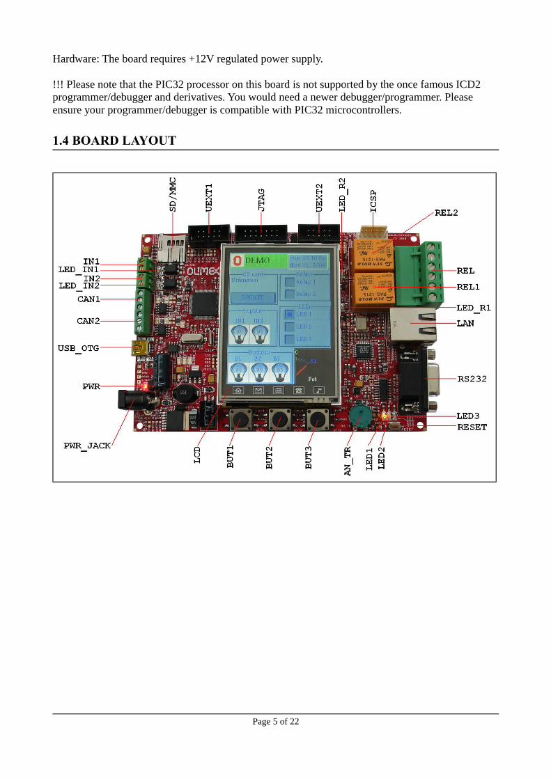
1.4 BOARD LAYOUT
Page 5 of 22
2. MICROCONTROLLER DETAILS
Some of the details about the main microcontroller in PIC32-MAXI-WEB (PIC32MX795F512L) microcontroller are mentioned in this chapter. It is highly recommended to refer to the original datasheet which might be downloaded from the official Microchip web-side.
2.1 FEATURES
PIC32-MAXI-WEB board uses MCU PIC32MX795F512L from Microchip Technology that packs the following features:
High-Performance 32-bit RISC CPU: MIPS32® M4K® 32-bit core with 5-stage pipeline 80 MHz maximum frequency 1.56 DMIPS/MHz (Dhrystone 2.1) performance at zero Wait state Flash access Single-cycle multiply and high-performance divide unit MIPS16e™ mode for up to 40% smaller code size Two sets of 32 core register files (32-bit) to reduce interrupt latency Prefetch Cache module to speed execution from Flash
Microcontroller Features: Operating voltage range of 2.3V to 3.6V 512K Flash memory (plus an additional 12 KB of Boot Flash) 128K SRAM memory Pin-compatible with most PIC24/dsPIC® DSC devices Multiple power management modes Multiple interrupt vectors with individually programmable priority Fail-Safe Clock Monitor mode Configurable Watchdog Timer with on-chip Low-Power RC oscillator for reliable operation
Peripheral Features: Atomic SET, CLEAR and INVERT operation on select peripheral registers 8-channels of hardware DMA with automatic data size detection USB 2.0-compliant full-speed device and On-The-Go (OTG) controller:
Dedicated DMA channels 10/100 Mbps Ethernet MAC with MII and RMII interface:
Dedicated DMA channels CAN module:
2.0B Active with DeviceNet™ addressing support Dedicated DMA channels
3 MHz to 25 MHz crystal oscillator Internal 8 MHz and 32 kHz oscillators Six UART modules with:
RS-232, RS-485 and LIN 1.2 support IrDA® with on-chip hardware encoder and decoder
Four SPI modules Five I2C™ modules Separate PLLs for CPU and USB clocks Parallel Master and Slave Port (PMP/PSP) with 8-bit and 16-bit data, and up to 16 address
Page 6 of 22
lines Hardware Real-Time Clock and Calendar (RTCC) Five 16-bit Timers/Counters (two 16-bit pairs combine to create two 32-bit timers) Five Capture inputs Five Compare/PWM outputs Five external interrupt pins High-speed I/O pins capable of toggling at up to 80 MHz High-current sink/source (18 mA/18 mA) on all I/O pins Configurable open-drain output on digital I/O pins
Debug Features: Two programming and debugging Interfaces:
2-wire interface with unintrusive access and real-time data exchange with application 4-wire MIPS® standard enhanced Joint Test Action Group (JTAG) interface
Unintrusive hardware-based instruction trace IEEE Standard 1149.2 compatible (JTAG) boundary scan
Analog Features: 16-channel, 10-bit Analog-to-Digital Converter:
1 Msps conversion rate Conversion available during Sleep and Idle
Two Analog Comparators 5V tolerant input pins (digital pins only)
Page 7 of 22
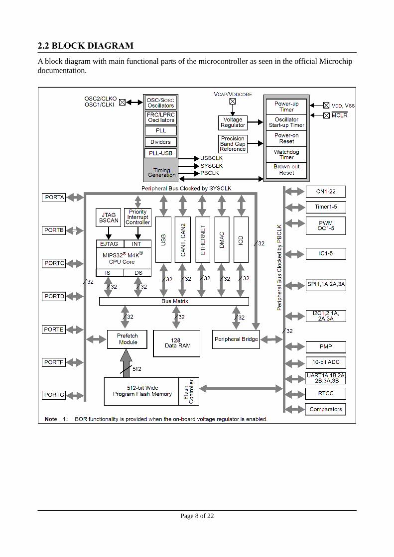
2.2 BLOCK DIAGRAM
A block diagram with main functional parts of the microcontroller as seen in the official Microchip documentation.
Page 8 of 22
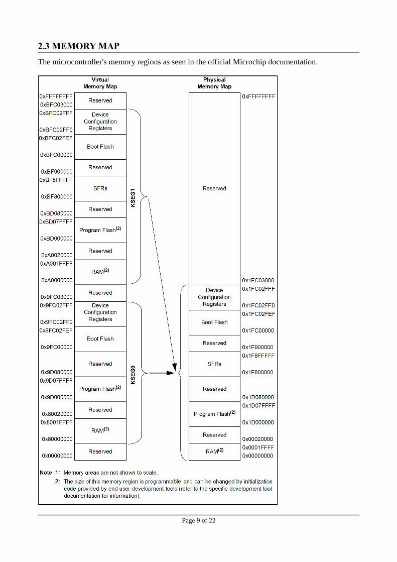
2.3 MEMORY MAP
The microcontroller's memory regions as seen in the official Microchip documentation.
Page 9 of 22
3 BOARD SCHEMATIC AND DIMENSIONS
In this chapter you may find information about the schematics describing logically and physically PIC32-MAXI-WEB.
3.1 SCHEMATIC
The schematic of PIC32-MAXI-WEB is available for reference on the next page.
Only the board schematic is available to the customer. It is available only as a stand-alone PDF document and as a reference image on. The board design files are kept private.
If you are looking for a schematic of an older revision of the board and it isn't available at our web site you may request it by the support e-mail.
Page 10 of 22
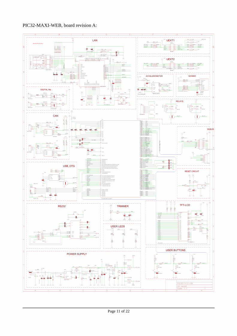
PIC32-MAXI-WEB, board revision A:
Page 11 of 22
12VDC
DEBUG INTERFACE:
POWER SUPPLY
RS232
USER LEDS
RESET CIRCUIT
CUT!!!NC
NC
USER BUTTONS
TRIMMER
USB_OTG
TFT-LCD
CAN
See LPC2378-STK_Rev.C
LAN UEXT1
UEXT2
SD/MMCACCELEROMETER
RELAYS
DIGITAL INs
3.3V
3.3VA1 23.3VA_E
CLOSE
3.3V_ECLOSE
AGND1 2AGND_E
CLOSE
AN_TR
10k
BUT1 BUT2 BUT3
C1100nF
C2100nF
C3100nF
C4100nF
C5100nF
C6100nF
C7 39pF
C8 39pF
C9 27pF
C10 27pF
C11100nF
C12
10uF/6.3V/0805
C13 100nF
+C14 10uF/6.3V/0805
C15 100nF
C16100nF
C20
10uF/6.3V/0805
C21
100nF C22100nF
+C23
10uF/6.3V/0805
C25C26
100nFC27
100nF
C2847uF/6.3V/TANT
C29100nF
C30
C31100nF
C32
100nF
C33
100nF
C34
NA(100nF)
C35
NA(100nF)
C36
NA(100nF)
C37
100nF
C38
C39
C40C41
C45NA(10nF)
C46
4.7nF
C51100nF
C52
10uF/6.3V/0805
C53100nF
C54
100nF
C55100nF
C56
100nF
C57100nF
C58
2.2uF
C59
100nF
C60
100nF
C61
100nF
C62
100nF
C63
10uF/6.3V
C64
47uF/6.3V/TANT
123
CAN1
TB3-3.5mm
12CAN1_D
OPEN
12
3
CAN2
TB3-3.5mm
12CAN2_D
OPEN
VDD
VSSOUT
E/D1
3
4
2
CD1
6NC2-50MHz
CTS
D1
1N4148
D2
1N4148
D31N5819(SS14)
D41N4148
D51N5819(SS14)
D61N5819(SS14)
D71N4148
D81N4148
FB1FB0805/600R/200mA(201209-601)
FB2FB0805/600R/200mA(201209-601)
FB4
FB0805/600R/200mA(201209-601)
FET1IRLML6402
GND
12
345
6
ICSP
WF6S
TB2-3.5mm
IN1
1
2
TB2-3.5mm
IN2
1
2
1 23 45 6
7 89 10
11 1213 14
JTAG
BH14S(PIN<12>-CUT\!)
L1
15uH/DBS135
L2CL470nH/0805/1.76R/250mA
7575
7575
1nF/2kV
1:1
1:1
1452
3786
GREEN
YELLOW
AGAG
AYAY
COM3
KGKG
KYKY
NC6
RD+7
RD-8
TD+1
TD-2
LAN
RJLBC-060TC1
LED1 LED2 LED3
LED_IN1GYX-SD-TC0805SURK(RED)
LED_IN2GYX-SD-TC0805SURK(RED)
OPT1
H11A817SMD
1
2
4
3
OPT2
H11A817SMD
1
2
4
3
+5V
2.5V
+5V
+12V
+12V+12V
+5V
+5V
PWRPWR_JACK
YDJ-1134
Q1
Q8.000MHz/20pF/HC-49SM(SMD)
GND
Q2QCT32768(2x6)/6pF
R61.5K/1%
R74.99k/1%
R8 10k
R910k
R10 1k
R16 100k
R22 4.7k
R23 330RR24 330RR25 330RR26 NA
R27 1k
R28 4.7k
0RR29 0R(NA)R30 NAR31 NA
R32 NA
R33 4.7k
0RR34 0R(NA)R35 NAR36 NA
R37 10k
0RR38 0R(NA)R39 NAR40 4.7k
0RR41 0R(NA)R42 NAR43 4.7k
R44 10k
R45 1MR46 10k
R47 100kR48 100kR49 100k
R50 1k
0R
R510R(NA)
R521k
R531k
R54 330R
R5510k
R56330R
R57NA
R58NA
R59NA
R60100k
R61100k
0R
R62
0R(NA)R63100k
R641k
R65330R
R66NA(100R)
R6710k
R68330R
R69NA(100R)
R7010k
R71330R
R72NA(100R)
R7310k
R74
R75
R76
R77
4.99k/1%
R78
15k/1%R79 4.99k/1%
R80
150k
R81
4.7k
R83330R
R84330R
R85330R
R86
330R
R87330R
R88NA
R8910kR9010k
0RR910R(NA)
R9410k
R95120R
0RR960R(NA)
R99 10k
R100120R
R101
4.7k
R102330R
R103330R
R104
4.7k
R105330R
1
234
5
6
REL
HD-515R_6P
RAS-12-15
REL1REL1
RAS-12-15
REL2
REL2
RESET
T1107A(6x3.8x2.5mm)
1
23
4
5
67
8
9
G1
G2
RS232
DB9-F
RTS
CD/DAT3/CS2
CLK/SCLK5
CMD/DI3
DAT0/DO7
DAT1/RES8
DAT2/RES1
VDD4
VSS6
SD/MMCMICRO
T1DTC114YKA
10k T2DTC114YKA
10k
T3DTC114YKA
10k
TFT
FS-K320QVB-V1
#CS4
#RD7
#RESET8
#WR6
DB09DB110DB211DB312DB413DB514DB615DB716DB817DB918DB1019DB1120DB1221DB1322DB1423DB1524
GND1
GND25
GND37
LEDA35
LEDA36
LEDK130
LEDK231
LEDK332
LEDK433
LEDK534
RS5
VCC2
VCC3
XL27
XR29
YD26
YU28
#MCLR13
#SS1/IC2/RD969
AC1RX/#SS3A/U3BRX/U3ACTS/RF1240
AC1TX/SCK3A/U3BTX/#U3ARTS/RF1339
AERXD0/INT1/RE818
AERXD1/INT2/RE919
AERXERR/RG151
AETXCLK/SCL1/INT3/RA1466
AETXD0/#SS1A/U1BRX/#U1ACTS/CN20/RD1447AETXD1/SCK1A/U1BTX/#U1ARTS/CN21/RD1548
AETXEN/SDA1/INT4/RA1567
AN2/C2IN-/CN4/RB223AN3/C2IN+/CN5/RB322AN4/C1IN-/CN6/RB421AN5/C1IN+/VBUSON/CN7/RB520
AN8/C1OUT/RB832AN9/C2OUT/RB933AN10/CVREFOUT/PMA13/RB1034AN11/ERXERR/AETXERR/PMA12/RB1135AN12/ERXD0/AECRS/PMA11/RB1241AN13/ERXD1/AECOL/PMA10/RB1342AN14/ERXD2/AETXD3/PMALH/PMA1/RB1443AN15/ERXD3/AETXD2/OCFB/PMALL/PMA0/CN12/RB1544
AVDD30
AVSS31
C1RX/ETXD1/PMD11/RF087
C1TX/ETXD0/PMD10/RF188
C2RX/PMD8/RG090
C2TX/ETXERR/PMD9/RG189
D+/RG257
D-/RG356
ECOL/SCK2A/U2BTX/#U2ARTS/PMA5/CN8/RG610
ECRS/SDA2A/SDI2A/U2ARX/PMA4/CN9/RG711
EMDC/IC4/PMCS1/PMA14/RD1171
ERXCLK/#SS2A/U2BRX/#U2ACTS/PMA2/CN11/RG914
ERXDV/SCL2A/SDO2A/U2ATX/PMA3/CN10/RG812
ETXCLK/PMD15/CN16/RD784
ETXD2/IC5/PMD12/RD1279ETXD3/PMD13/CN19/RD1380
ETXEN/PMD14/CN15/RD683
OC2/RD176OC3/RD277OC4/RD378
OC5/PMWR/CN13/RD481
OSC1/CLKI/RC1263OSC2/CLKO/RC1564
PGEC1/AN1/CN3/RB124
PGEC2/AN6/OCFA/RB626
PGED1/AN0/CN2/RB025
PGED2/AN7/RB727
PMD0/RE093PMD1/RE194PMD2/RE298PMD3/RE399
PMD4/RE4100
PMD5/RE53
PMD6/RE64
PMD7/RE75
PMRD/CN14/RD582
RTCC/EMDIO/IC1/RD868
SCK1/IC3/PMCS2/PMA15/RD1070
SCL1A/SDO1A/U1ATX/RF853
SCL2/RA258
SCL3A/SDO3A/U3ATX/PMA8/CN18/RF550
SDA1A/SDI1A/U1ARX/RF252
SDA2/RA359
SDA3A/SDI3A/U3ARX/PMA9/CN17/RF449
SDO1/OC1/INT0/RD072
SOSCI/CN1/RC1373
SOSCO/T1CK/CN0/RC1474
T2CK/RC16T3CK/AC2TX/RC27T4CK/AC2RX/RC38T5CK/SDI1/RC49
TCK/RA138
TDI/RA460TDO/RA561
TMS/RA017
TRCLK/RA691
TRD0/RG1397
TRD1/RG1296
TRD2/RG1495
TRD3/RA792
USBID/RF351
VBUS54
VCAP/VDDCORE85
VDD2
VDD16
VDD37
VDD46
VDD62
VDD86
VREF+/CVREF+/AERXD3/PMA6/RA1029
VREF-/CVREF-/AERXD2/PMA7/RA928VSS
15
VSS36
VSS45
VSS65
VSS75
VUSB55
U1
PIC32MX795F512L-80I/PT
FXSD/FXEN34
GND18
GND212
GND435
GND536
INT/PHYAD025
LED0/TEST26
LED1/SPD100/NFEF27
LED2/DUPLEX28
LED3/NWAYEN29
MDC2
MDIO1
PD#30
RX+33RX-32
RXC10
RXD0/PHYAD46
RXD1/PHYAD35
RXD2/PHYAD24
RXD3/PHYAD13
RXDV/CRSDV/PCS_LPBK9
RXER/ISO11
VDDIO17
VDDRX31
U2KS8721BLMM
U3
SMB380,(QFN10)
CSB5GND
3
INT 4
NC11
NC210
SCK6
SDI/SDA8
SDO7
VDD2
VDDIO9
GND
VCCRESET1 2
U4NA(MCP130T)
C1+1
C1-3
C2+4
C2-5
R1IN13R1OUT
12R2IN8
R2OUT9
T1IN11T1OUT14
T2IN10T2OUT7
V+2
V-6
U5
ST3232(SO16)
GND VCC15 16
U5PWR
#ENA1
#ENB4
FLAG_A2
FLAG_B3GND6
IN7
OUT_A8
OUT_B5
U6
LM3526M-L(SO8)
CANH7CANL6
RS8
RXD4
TXD1
VDD3
VREF5
VSS2
U7
MCP2551
CANH7CANL6
RS8
RXD4
TXD1
VDD3
VREF5
VSS2
U8
MCP2551
BH10S
UEXT1
1 23 45 6
7 89 10
BH10S
UEXT2
1 23 45 6
7 89 10
D+
D-
GNDID
VBUS
USB_OTG
MICRO_AB
3.3V
3.3V
3.3VA
3.3V3.3V
3.3V
3.3V
3.3V
3.3V
3.3V
3.3V
3.3V
3.3V
3.3V3.3V
3.3V
AGNDAGND AGND
3.3VA
3.3V3.3V 3.3V
3.3V
3.3V
3.3V
3.3V
3.3V
3.3V
3.3V
3.3V
3.3V
3.3V
3.3V
3.3V
3.3V
3.3V
3.3V
3.3V
3.3V
3.3V3.3V
3.3V
3.3V3.3V
3.3V
3.3V
3.3V
3.3VA
AGND
AGND
3.3V
3.3V3.3V
VDD_ECLOSE
VR1
BD9778HFP
EN/SYNC7
FB 3GND
4
INV 5
RT6 SW 2
VIN1
ADJ/GND
IN OUT
VR1(3.3V)LM1117IMPX-ADJ
+5V_VBUS +5V_VBUS
+5V_VBUS
/TFT_CS
/TFT_CS
/TFT_RST
/TFT_RST
AC1RX
AC1RX
AC1RX
AC1TX/SCK3A
AC1TX/SCK3A
AC1TX/SCK3A
AC1TX/SCK3A
AC2RX
AC2RX
AC2TX
AC2TX
ACC_INT
ACC_INT
AERXD0
AERXD0
AERXD1
AERXD1
AERXERR
AERXERR
AETXD0AETXD1
AETXEN
AETXEN
CS_MMC
CS_MMC
EMDC
EMDC
EMDIO
EMDIO
ERXDV
ERXDV
IN1
IN1
IN2
IN2
LED1
LED1
LED2
LED2
LED3
LED3
MISO1
MISO1
MISO3A
MISO3A
MISO3A
MISO3A
MOSI1
MOSI1
MOSI3A
MOSI3A
MOSI3A
MOSI3A
PC_CD PC_CTS
PC_CTS PC_RTSPC_RTS
PC_RXD
PC_RXD
PC_TXD PC_TXD
PGEC2
PGEC2
PGED2
PGED2
PHY_IRQ
PHY_IRQ
PHY_IRQ
PHY_REFCLK
PHY_REFCLK
PHY_RSTN
PHY_RSTN
PHY_VDD_PLL
PMD0
PMD0
PMD1
PMD1
PMD2
PMD2
PMD3
PMD3
PMD4
PMD4
PMD5
PMD5
PMD6
PMD6
PMD7
PMD7
PMD8
PMD8
PMD9
PMD9PMD10
PMD10
PMD11
PMD11 PMD12
PMD12
PMD13
PMD13
PMD13
PMD14
PMD14
PMD14 PMD15
PMD15
PMD15
PMRD
PMRD
PMWR
PMWR
RELAY1
RELAY1
RELAY2
RELAY2
RSTN
RSTN
RSTN
RSTN
RXD1
RXD1
RXD1
RXD1_INT
RXD1_INT
SCK1
SCK1
SCL1
SCL2
SCL2
SCL2
SDA1
SDA2
SDA2
SDA2
SW_SCL1
SW_SCL1
SW_SDA1
SW_SDA1
SW_U2RX
SW_U2RX
SW_U2TX
SW_U2TX
TCK
TCK
TDI
TDI
TDO
TDO
TFT_LIGHT
TFT_LIGHT
TFT_RS
TFT_RS
TMS
TMS
TRIM
TRIM
TXD1
TXD1
TXD1
U2RXU2TX
UEXT1_CS
UEXT1_CS
UEXT2_CS
UEXT2_CS
USBID
USBID USBIDUSB_D+USB_D+
USB_D+USB_D-
USB_D-USB_D-
USB_FAULT
USB_FAULT
VBUSON
VBUSON
XL
XL
XR
XR
YD
YD
YU
YU
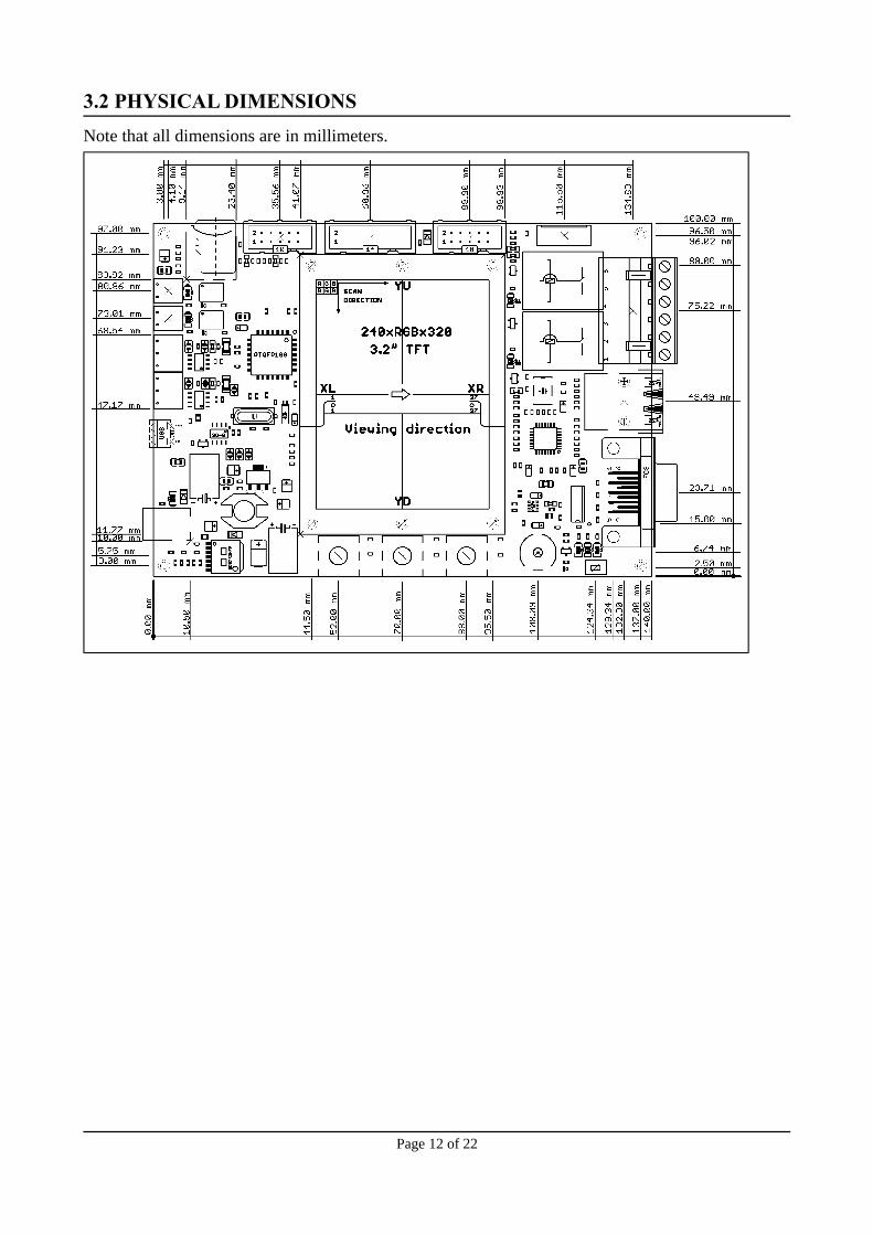
3.2 PHYSICAL DIMENSIONS
Note that all dimensions are in millimeters.
Page 12 of 22

4. CONTROL CIRCUITRY
4.1 POWER SUPPLY CIRCUIT
PIC32-MAXI-WEB can be power only from power connector PWR_JACK, where only 12 VDC external voltage source has to be applied.
The board power consumption is about 300mA with all peripherals and MCU running at full speed, relays and LEDs on and established Ethernet connection.
4.2 RESET CIRCUIT
PIC32-MAXI-WEB reset circuit is made of D4 (1N4148), RC group R55 – 10k and C31 – 100nF. Serial resistor R56 – 330Ω is used to prevent fast C31 charge and discharge when PIC32MX795F512L is being programmed.
Manual reset is possible by the RESET button.
4.3 CLOCK CIRCUIT
Quartz crystal Q1 8MHz is connected to PIC32MX795F512L pins 63 (OSC1/CLKI/RC12) and 64 (OSC2/CLKO/RC15).
Quartz crystal Q2 32.768 KHz is connected to PIC32MX795F512L pins 73 (SOSCI/CN1/RC13) and 74 (SOSCO/T1CK/CN0/RC14).
Page 13 of 22
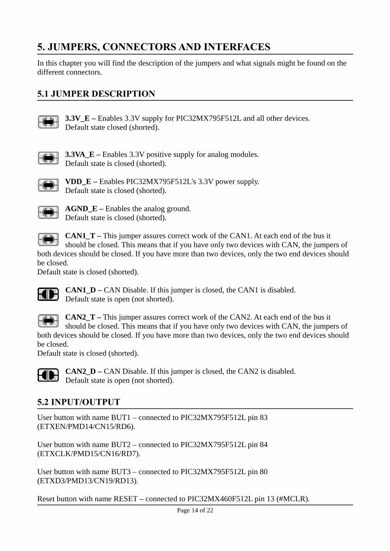
5. JUMPERS, CONNECTORS AND INTERFACES
In this chapter you will find the description of the jumpers and what signals might be found on the different connectors.
5.1 JUMPER DESCRIPTION
3.3V_E – Enables 3.3V supply for PIC32MX795F512L and all other devices.Default state closed (shorted).
3.3VA_E – Enables 3.3V positive supply for analog modules.Default state is closed (shorted).
VDD_E – Enables PIC32MX795F512L's 3.3V power supply.Default state is closed (shorted).
AGND_E – Enables the analog ground.Default state is closed (shorted).
CAN1_T – This jumper assures correct work of the CAN1. At each end of the bus it should be closed. This means that if you have only two devices with CAN, the jumpers of
both devices should be closed. If you have more than two devices, only the two end devices should be closed.Default state is closed (shorted).
CAN1_D – CAN Disable. If this jumper is closed, the CAN1 is disabled.Default state is open (not shorted).
CAN2_T – This jumper assures correct work of the CAN2. At each end of the bus it should be closed. This means that if you have only two devices with CAN, the jumpers of
both devices should be closed. If you have more than two devices, only the two end devices should be closed.Default state is closed (shorted).
CAN2_D – CAN Disable. If this jumper is closed, the CAN2 is disabled.Default state is open (not shorted).
5.2 INPUT/OUTPUT
User button with name BUT1 – connected to PIC32MX795F512L pin 83 (ETXEN/PMD14/CN15/RD6).
User button with name BUT2 – connected to PIC32MX795F512L pin 84 (ETXCLK/PMD15/CN16/RD7).
User button with name BUT3 – connected to PIC32MX795F512L pin 80 (ETXD3/PMD13/CN19/RD13).
Reset button with name RESET – connected to PIC32MX460F512L pin 13 (#MCLR).
Page 14 of 22
One analog trimmer with name AN_TR – connected to PIC32MX795F512L pin 32 (AN8/C1OUT/RB8).
Status Led (yellow) with name LED1 – connected to PIC32MX795F512L pin 34 (AN10/CVREFOUT/PMA13/RB10).
Status Led (green) with name LED2 – connected to PIC32MX795F512L pin 76 (OC2/RD1).Status Led (red) with name LED3 – connected to PIC32MX795F512L pin 77 (OC3/RD2).
Two opto-isolated digital inputs IN1 and IN2.
Two red LEDs – LED_IN1 and LED_IN2 for every digital input.
Two red LEDs – LED_R1, LED_R2 – for the relays.
Power supply red LED with name PWR – indicates that 3.3V power supply is available.
TFT LCD Display – FS-K320QVB-V1
5.3 EXTERNAL CONNECTOR DESCRIPTION
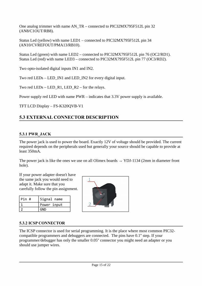
5.3.1 PWR_JACK
The power jack is used to power the board. Exactly 12V of voltage should be provided. The current required depends on the peripherals used but generally your source should be capable to provide at least 350mA.
The power jack is like the ones we use on all Olimex boards → YDJ-1134 (2mm in diameter front hole).
If your power adapter doesn't havethe same jack you would need toadapt it. Make sure that youcarefully follow the pin assignment.
Pin # Signal name
1 Power input2 GND
5.3.2 ICSP CONNECTOR
The ICSP connector is used for serial programming. It is the place where most common PIC32-compatible programmers and debuggers are connected. The pins have 0.1'' step. If your programmer/debugger has only the smaller 0.05'' connector you might need an adapter or you should use jumper wires.
Page 15 of 22
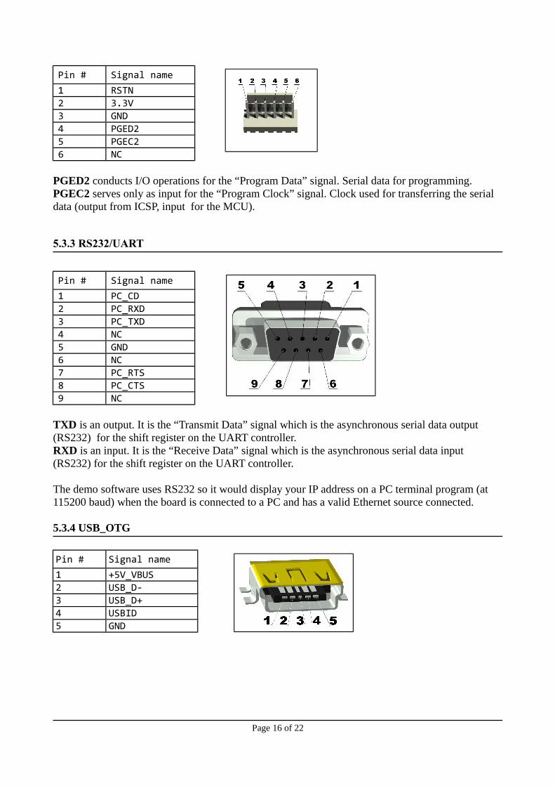
Pin # Signal name
1 RSTN2 3.3V3 GND4 PGED25 PGEC26 NC
PGED2 conducts I/O operations for the “Program Data” signal. Serial data for programming.PGEC2 serves only as input for the “Program Clock” signal. Clock used for transferring the serial data (output from ICSP, input for the MCU).
5.3.3 RS232/UART
Pin # Signal name
1 PC_CD2 PC_RXD3 PC_TXD4 NC5 GND6 NC7 PC_RTS8 PC_CTS9 NC
TXD is an output. It is the “Transmit Data” signal which is the asynchronous serial data output (RS232) for the shift register on the UART controller.RXD is an input. It is the “Receive Data” signal which is the asynchronous serial data input (RS232) for the shift register on the UART controller.
The demo software uses RS232 so it would display your IP address on a PC terminal program (at 115200 baud) when the board is connected to a PC and has a valid Ethernet source connected.
5.3.4 USB_OTG
Pin # Signal name
1 +5V_VBUS2 USB_D-3 USB_D+4 USBID5 GND
Page 16 of 22

5.3.5 ETHERNET
Pin # Signal name(chip side) Pin # Signal name(chip side)1 TX+ 5 Not Connected (NC)2 TX- 6 Not Connected (NC)3 VCC/2 (2.5V) 7 RX+4 Not Connected (NC) 8 RX-
LED Color UsageLeft Yellow 100MBits/s (Half/Full duplex)Right Green Activity
5.3.6 CAN1 AND CAN2
Controller Area Network(CAN) is a standard designed to allow microcontrollers and devices to communicate with each other within a vehicle without a host computer. Both CAN1 and CAN2 connectors follow the same layout.
Pin # Signal
1 GND2 CANL3 CANH
5.3.7 JTAG
The microcontroller has EJTAG support. The EJTAG signals are provided on the 14-pin JTAG connector.
Pin # Signal name Pin # Signal name
1 NC 8 GND2 GND 9 TCK3 TDI 10 GND4 GND 11 RSTN5 TDO 12 CUT6 GND 13 NC7 TMS 14 3.3v
Page 17 of 22
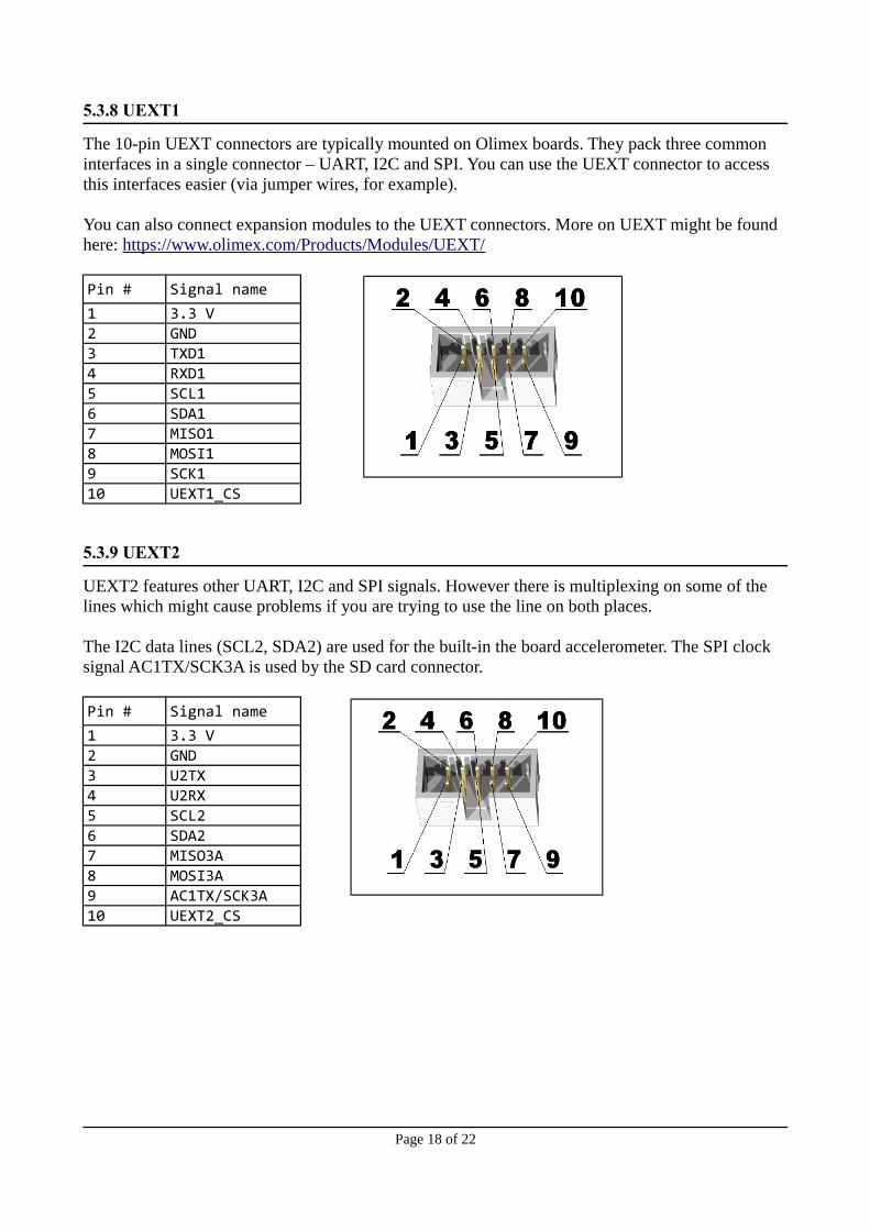
5.3.8 UEXT1
The 10-pin UEXT connectors are typically mounted on Olimex boards. They pack three common interfaces in a single connector – UART, I2C and SPI. You can use the UEXT connector to access this interfaces easier (via jumper wires, for example).
You can also connect expansion modules to the UEXT connectors. More on UEXT might be found here: https://www.olimex.com/Products/Modules/UEXT/
Pin # Signal name
1 3.3 V2 GND3 TXD14 RXD15 SCL16 SDA17 MISO18 MOSI19 SCK110 UEXT1_CS
5.3.9 UEXT2
UEXT2 features other UART, I2C and SPI signals. However there is multiplexing on some of the lines which might cause problems if you are trying to use the line on both places.
The I2C data lines (SCL2, SDA2) are used for the built-in the board accelerometer. The SPI clock signal AC1TX/SCK3A is used by the SD card connector.
Pin # Signal name
1 3.3 V2 GND3 U2TX4 U2RX5 SCL26 SDA27 MISO3A8 MOSI3A9 AC1TX/SCK3A10 UEXT2_CS
Page 18 of 22

5.3.10 MICROSD CARD
Pin # Signal name
1 MCIDAT22 CS_MMC3 MOSI3A4 VDD (3.3 V)5 AC1TX/SCK3A6 GND7 MISO3A8 MCIDAT19 Not Connected10 Not Connected11 Not Connected12 Not Connected
Page 19 of 22
6. AVAILABLE DEMO SOFTWARE
To compile the demo you would need the following tools: MPLAB IDE v8.91 or MPLABX 1.80, Compiler: XC32 v1.21.
The demo demonstrates the functionality of the various peripherals of the board including user input, serial communication, the implementation of Graphical User Interface (GUI) and betwork connectivity
The demo is built upon the Microchip Solutions library (released on 22 august 2012) including freely distributed support libraries:
- Microchip Graphics Library v3.06- Microchip TCP/IP Stack Library v5.42- Microchip MDD File System Library 1.4.0 (FAT, FAT32 file systems)- Microchip USB support source files
FreeRTOS was used to make all tasks run virtually simultaneously. FreeRTOS is a freely distributedRTOS with excellent support and online documentation. Version used is v7.3.0. MPLAB has support for FreeRTOS (Tools/RTOS viewer).
You could find demo software for PIC32-MAXI-WEB board at the board's web page. It is recommended to refer to the “README.txt” file inside the demo archive.
Direct link to PIC32-MAXI-WEB's web-page: https://www.olimex.com/Products/PIC/Development/PIC32-MAXI-WEB/
Page 20 of 22
7. REVISION AND ORDERING INFORMATION
PIC32-MAXI-WEB – fully assembled and tested
How to purchase?
You can purchase directly from our online shop or from any of our distributors. Note that usually it is faster and cheaper to purchase Olimex products from our distributors. List of confirmed Olimex LTD distributors and resellers: https://www.olimex.com/Distributors.
Please visit https://www.olimex.com/ for more info.
7.1 DOCUMENT REVISION
Revision, date Changes Modified page
A, 30.08.13 Initial manual release All
B, 03.12.13 Document remake All
C, 30.10.15 Fixed a number of errors All
7.2 BOARD REVISION
Remember to check the schematics and the board design files to compare the differences.
Revision Notable changes
A Initial release of the board
Page 21 of 22

8. WARRANTY AND SUPPORT
For product support, hardware information and error reports mail to: [email protected]. All document or hardware feedback is welcome. Note that we are primarily a hardware company and our software support is limited. Please consider reading the paragraph below about the warranty of Olimex products.
All goods are checked before they are sent out. In the unlikely event that goods are faulty, they must be returned, to OLIMEX at the address listed on your order invoice.
OLIMEX will not accept goods that have clearly been used more than the amount needed to
evaluate their functionality.
If the goods are found to be in working condition, and the lack of functionality is a result of
lack of knowledge on the customers part, no refund will be made, but the goods will be returned
to the user at their expense.
All returns must be authorized by an RMA Number. Email [email protected] for authorization
number before shipping back any merchandise. Please include your name, phone number and order
number in your email request.
Returns for any unaffected development board, programmer, tools, and cables permitted within 7
days from the date of receipt of merchandise. After such time, all sales are considered final.
Returns of incorrect ordered items are allowed subject to a 10% restocking fee. What is
unaffected? If you hooked it to power, you affected it. To be clear, this includes items that
have been soldered to, or have had their firmware changed. Because of the nature of the
products we deal with (prototyping electronic tools) we cannot allow returns of items that have
been programmed, powered up, or otherwise changed post shipment from our warehouse.
All returned merchandise must be in its original mint and clean condition. Returns on damaged,
scratched, programmed, burnt, or otherwise 'played with' merchandise will not be accepted.
All returns must include all the factory accessories which come with the item. This includes
any In-Circuit-Serial-Programming cables, anti-static packing, boxes, etc.
With your return, enclose your PO#. Also include a brief letter of explanation of why the
merchandise is being returned and state your request for either a refund or an exchange.
Include the authorization number on this letter, and on the outside of the shipping box.
Please note: It is your responsibility to ensure that returned goods reach us. Please use a
reliable form of shipping. If we do not receive your package we will not be held liable.
Shipping and handling charges are not refundable. We are not responsible for any shipping
charges of merchandise being returned to us or returning working items to you.
The full text might be found at https://www.olimex.com/wiki/GTC#Warranty for future reference.
Page 22 of 22