Embed Size (px)
Citation preview
Picosecond UV Single Photon Detectors with Lateral Drift Field: Concept and
Technologies
M. Yakimov1, S. Oktyabrsky
1 and P. Murat
2*
a SUNY College of Nanoscale Science and Engineering, Albany, NY 12203, USA
b Fermi National Accelerator Laboratory, Batavia, IL, 60510, USA
Group III-V semiconductor materials are being considered as a Si replacement for advanced
logic devices for quite some time. Advances in III-V processing technologies, such as interface
and surface passivation, large area deep submicron lithography with high-aspect ratio etching
primarily driven by the MOSFET development can also be used for other applications. In this
paper we will focus on photodetectors with the drift field parallel to the surface. We compare the
proposed concept to the state-of-the-art Si-based technology and discuss requirements which
need to be satisfied for such detectors to be used in a single photon counting mode in blue and
ultraviolet spectral region with about 10 ps photon timing resolution essential for numerous
applications ranging from high-energy physics to medical imaging.
____________
* Contact author, email: [email protected]
1. Introduction
After over 40 years of successful development of various kinds of semiconductor photodetectors
(PDs), it is quite surprising that there are still many applications utilizing vacuum tubes for light
detection. It is true that for fast detectors electron transport in vacuum has a fundamental
advantage over the transport in solids: lack of scattering that results in higher electron velocities
and allows for reduction of internal capacitance of the vacuum device. On the other hand, recent
progress in scaling of semiconductor devices and introduction of novel, other than silicon,
materials into integrated circuit technologies provide new possibilities to fill the gaps between
semiconductor and vacuum PDs. One of the gaps is a high-speed PD with large sensitive area
and high single photoelectron sensitivity in the UV region that is required in various areas of
scientific research and industry.
A number of such applications come from particle physics and astrophysics. Many modern dark
matter and neutrino detectors use liquidified noble gases, LAr or LXe, which emit scintillating
light at 128 nm and 175 nm, respectively. In absence of photodetectors sensitive at these
wavelengths, the most common technique of detecting the emitted UV light is relying on the
wavelength shifting [1]. At LHC, to identify individual proton-proton interactions and separate
interactions of interest from the background in high-luminosity mode, the experiments will need
timing detectors with picosecond-level resolution [2]. Detection of UV photons in the range of
90-300 nm also sheds light on many important processes in astrophysics [3]. Another application
area which could greatly benefit from very fast photodetectors is the positron emission
tomography (PET). PET scanners with timing resolution of the order of 10 ps could have
significantly improved sensitivity leading to a breakthrough in the early diagnostics of cancer
diseases. Progress in PET, however, also depends on the development of new fast scintillators
which often, like in case of BaF2 or LaBr3, emit significant fraction of light in the UV region and
require UV-sensitive photodetectors to read the signals out [4, 5].
Solid state PDs can provide separately ultra-high speed response and single photoelectron
sensitivity [6, 7]. The best timing response is typically achieved in group III-V semiconductor p-
i-n or metal-semiconductor-metal (MSM) PDs, while single photoelectron response requires
avalanche multiplication region and low dark count rates that are best realized in Si p-i-n diodes
and more recently were demonstrated in III-V diodes [8, 9]. State of the art Si solid state
photomultipliers (Si avalanche diodes with on-chip signal processing circuits) demonstrate
single-photon sensitivity with ~100 ps range timing response and dark count of about 106 s
-1 cm
-
2. Their spectral sensitivity extends down to 300 nm, covering a large part of high-speed
scintillator emission spectrum.
Combining fast response and single-electron sensitivity with large sensitive area and high UV
quantum efficiency is even more challenging. Semiconductor surface has always been
considered a difficult part of a PD due to surface generation/recombination, surface leakage and
surface traps related instabilities. As a result, detectors with low dark current and high quantun
efficiency are typically made using bulk absorption in a vertical junction. Surface passivation
and guarding are used when high lateral electric fields are employed in avalanche junctions. In
the following, we discuss how the existing challenges can be addressed by using different
detector materials along with the specific design rules. In particular, close-to-surface UV
absorption with lateral field detector configuration allows for separate optimization of absorption
and multiplication cross-section areas to minimize capacitance and dark current.
2. Detector geometry
The fastest semiconductor PDs demonstrated so far utilize lateral metal-semiconductor-metal
(MSM) architecture (Fig. 1a). It has been proven to be reasonably easy to achieve rise-time
below 10 ps and even below 1ps if materials with short recombination times are used [10-13].
However, this comes at a cost of reduced PD efficiency. Significant difference between MSM
detectors and more commonly used p-i-n PDs is the difference in the drift field direction: the
drift field is parallel to the detector surface in MSM's and orthogonal to the surface in p-i-n PDs.
Both designs have their respective advantages and disadvantages in terms of temporal resolution
and spectral sensitivity. Capacitance and associated RC delay, transit time of photocarriers and
the absorption length are the major parameters affecting the timing and efficiency of the PD.
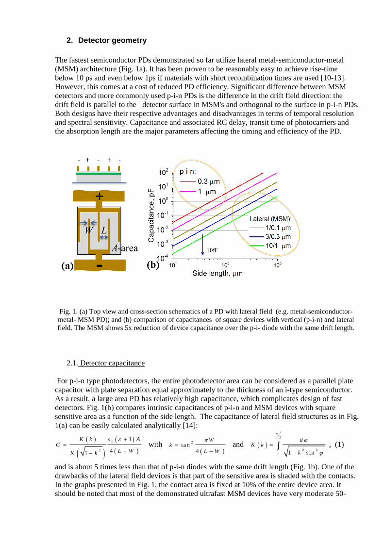
Fig. 1. (a) Top view and cross-section schematics of a PD with lateral field (e.g. metal-semiconductor-
metal- MSM PD); and (b) comparison of capacitances of square devices with vertical (p-i-n) and lateral
field. The MSM shows 5x reduction of device capacitance over the p-i- diode with the same drift length.
2.1. Detector capacitance
For p-i-n type photodetectors, the entire photodetector area can be considered as a parallel plate
capacitor with plate separation equal approximately to the thickness of an i-type semiconductor.
As a result, a large area PD has relatively high capacitance, which complicates design of fast
detectors. Fig. 1(b) compares intrinsic capacitances of p-i-n and MSM devices with square
sensitive area as a function of the side length. The capacitance of lateral field structures as in Fig.
1(a) can be easily calculated analytically [14]:
0
2
1
41
K k AC
L WK k
with
2tan
4
Wk
L W
and
2
2 2
0 1 s in
dK k
k
, (1)
and is about 5 times less than that of p-i-n diodes with the same drift length (Fig. 1b). One of the
drawbacks of the lateral field devices is that part of the sensitive area is shaded with the contacts.
In the graphs presented in Fig. 1, the contact area is fixed at 10% of the entire device area. It
should be noted that most of the demonstrated ultrafast MSM devices have very moderate 50-
70% sensitive area limited by the need for long low-resistance metal lines. However, novel IC
interconnect technologies using low-resistive Cu in high aspect ratio wires make 1 k(e.g.
0.1x0.1x30 m3) wires feasible. Using them would allow to increase significantly the sensitive
area of the device without affecting its intrinsic RC delay.
2.2.Transit drift time
Intrinsic time jitter of a PD is limited by the fluctuations transit time of faster photocarriers
(typically electrons) through the depletion region of the diode, which is determined by carrier
drift velocity.
Drift velocity saturates in high electric fields due to optical phonon scattering and places the
limit for intrinsic delay time. The delay may be reduced by thinning down the drift (depletion)
region but that increases the device capacitance. Therefore, to keep the capacitance low one
needs to further limit the sensitive area, In addition, thin sensitive layer may reduce the
absorption efficiency, although it is typically not the case in the blue/UV spectral region. The
interplay between the drift length and capacitance determines the device area and depletion
width for the required PD response time. Table 1 shows saturation properties and corresponding
device parameters for PDs with 10 ps rise-time built using different materials. One of the most
obvious advantages of III-V materials with low electron effective masses is the much higher
saturation drift velocity achieved at lower fields. Compared to Si p-i-n PDs, a 3x increase in the
electron drift velocity combined with 5x reduction of capacitance allows to improve the speed of
III-V PDs with lateral field by a factor of ~15. Alternatively, one could increase the PD sensitive
area by the same factor, keeping the timing response unchanged.
Table 1. Saturation field (Esat ), velocity (vsat), length for 10ps drift and corresponding operational voltage
( Vsat) for different PD materials.
Material Esat ,
kV/cm
Vsat ,
x105 m/s
Spacing for
10 ps, m
Vsat ,
V
Si 20 0.8 0.8 1.6
GaN 150 2.4 2.4 36
GaAs 3.5 2 2 0.7
InP 12 2.5 2.5 3
InGaAs/ InP 5 3 3 1.5
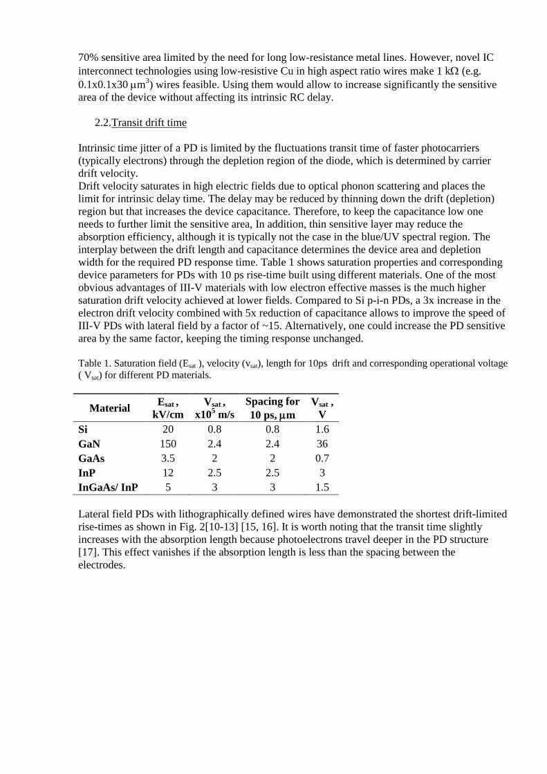
Lateral field PDs with lithographically defined wires have demonstrated the shortest drift-limited
rise-times as shown in Fig. 2[10-13] [15, 16]. It is worth noting that the transit time slightly
increases with the absorption length because photoelectrons travel deeper in the PD structure
[17]. This effect vanishes if the absorption length is less than the spacing between the
electrodes.
Fig. 2. Saturation velocity-limited electron drift transit time in various materials. Symbols indicate the
demonstrated MSM rise-times [10-13].
2.3.Spectral response
In order to create a p-i-n PD, a highly-doped conductive semiconductor layer needs to be formed
along the surface. That creates no issues for visible light detectors since light penetrates
reasonably deep into semiconductor. However, the short UV absorption length in most common
materials makes absorption within the doped layer a significant problem. In 300-400 nm interval,
the absorption coefficient in most of the III-V’s is about 7x105 cm
-1, and photocarriers are
generated in a ~20 nm thick surface layer. Silicon has even higher absorption >106 cm
-1 for the
wavelengths below 370 nm and, therefore, light is absorbed within just 10 nm from the surface.
Since a substantial number of photocarriers is generated in a highly doped contact region with
low electric field, the high absorption value significantly reduces quantum efficiency of Si p-i-n
devices in the UV region [18]. As a result, both detector efficiency and response time degrade
due to recombination and slower carrier diffusion in the highly-doped areas. In an effort to
reduce the thickness of the highly-doped contact layer, the inversion-layer and delta-doped
structures were introduced in so-called UV-enhanced PDs [19]. The latter design has shown a
very impressive UV efficiency up to 60% at the wavelengths down to 125 nm in small 4x4 m2
CCD pixels [20]. These approaches relying on reduction of the contact layer thickness inevitably
increase the lateral resistance of this layer connected in series and add up to the RC delay
detrimental for high-speed applications. In fact, a significant slow diffusion component of the
temporal response and relatively high attainable sheet resistivities close to ~10 k/sq. make the
design of ultrafast UV-enhanced PDs a real challenge.
Total elimination of highly-doped surface contact layer is possible in lateral field (e.g. MSM)
devices. The lateral field geometry becomes favorable when material/wavelength combination
with high absorption coefficients is employed, such as III-V semiconductors in blue and UV
spectral regions. The lateral field that exists on the very surface of the structure (as well as above
the surface) makes collection and drift of photocarriers efficient and fast.
Table 1 shows the operating parameters for several III-V semiconductor devices with the lateral
field. The required operating voltages are quite low in all the cases, except for GaN. In addition,
GaN being a wide-bandgap material has significantly higher absorption length which could
complicate design of a detector with a thin surface quantum well (QW) and could require a
different geometry and higher voltages.
One of the issues with the III-V materials is the high surface recombination rate which reduces
the response time but also degrades quantum efficiency. Modern surface and interface
passivation techniques developed for novel III-V MOSFETs [21] significantly reduce the
interface trap density and recombination rates so that the photocarrier drift transit time is not
affected. However, as described below, the surface/interface might still be a source of carrier
generation that affects the device dark current.
3. Dark Current and Dark Count Rate
Noise is a critical factor in any detector applications, but the need of high single photon quantum
efficiency makes the low noise requirement especially demanding. Despite the wider bandgap of
GaAs compared to Si, the dark current density in III-V photodetectors is higher than in Si PDs.
The reasons for the increased dark current appear to be technology-related, with the generation
(commonly called generation/recombination – GR) current within GaAs depletion region being a
primary source of dark current.
At reverse bias voltage saturating the drift velocity, there are two processes contributing to the
PD dark current: injection of carriers from the contacts and carrier generation in the
photosensitive (depletion) region of the semiconductor. An MSM detector fabricated with two
identical metal-semiconductor junctions would have at least one contact with the barrier height
of Eg/2 or less (Eg is the semiconductor bandgap). As a result, the dark current is mostly
determined by thermionic injection of carriers over the lowest MS barrier B :
(2)
In semiconductor PDs with p-n or p-i-n junctions, the dark current is dominated by the
generation in the depletion region, which include the bulk Shockley-Hall-Read (SHR) generation
and generation through surface states. The SHR dark current can be calculated as
, (3)
where Vdepl is the volume of high electric field (depletion) region, ni – intrinsic carrier
concentration, and 0 – carrier recombination lifetime (assuming equal lifetime for electrons and
holes). The surface component of the generation current depends on the PD geometry. For
example, in a p-i-n PD it is determined by the perimeter area with high electric field and surface
trap density.
Figure 3 shows a simulated dependence of dark current density vs. operating voltage in 1m
long/thick MSM or p-i-n PDs. The effect of thermionic emission on the barrier height of a
semiconductor contact and generation/recombination is clearly seen. For identical metal-
semiconductor junctions of an MSM detector, at least one of the barriers to GaAs with
Eg=1.42eV is ~0.7 eV or below, resulting in the injection current higher than ~30 A/cm2 at
room temperature [22, 23]. To reduce the thermionic current, a metal contact to a wider bandgap
material such as AlGaAs or InAlGaP is required [24-27]. A built-in heterojunction barrier close
2
i
S H R d ep l
o
nI q V
2~ exp
B
thermionic
qI T
kT
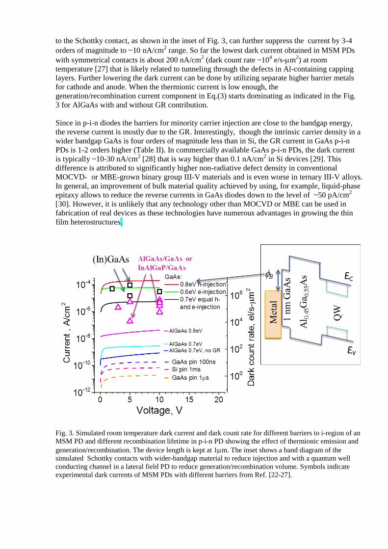
to the Schottky contact, as shown in the inset of Fig. 3, can further suppress the current by 3-4
orders of magnitude to ~1nA/cm2 range. So far the lowest dark current obtained in MSM PDs
with symmetrical contacts is about 200 nA/cm2 (dark count rate ~10
4 e/s-m
2) at room
temperature [27] that is likely related to tunneling through the defects in Al-containing capping
layers. Further lowering the dark current can be done by utilizing separate higher barrier metals
for cathode and anode. When the thermionic current is low enough, the
generation/recombination current component in Eq.(3) starts dominating as indicated in the Fig.
3 for AlGaAs with and without GR contribution.
Since in p-i-n diodes the barriers for minority carrier injection are close to the bandgap energy,
the reverse current is mostly due to the GR. Interestingly, though the intrinsic carrier density in a
wider bandgap GaAs is four orders of magnitude less than in Si, the GR current in GaAs p-i-n
PDs is 1-2 orders higher (Table II). In commercially available GaAs p-i-n PDs, the dark current
is typically ~10-30 nA/cm2 [28] that is way higher than 0.1 nA/cm
2 in Si devices [29]. This
difference is attributed to significantly higher non-radiative defect density in conventional
MOCVD- or MBE-grown binary group III-V materials and is even worse in ternary III-V alloys.
In general, an improvement of bulk material quality achieved by using, for example, liquid-phase
epitaxy allows to reduce the reverse currents in GaAs diodes down to the level of ~50 pA/cm2
[30]. However, it is unlikely that any technology other than MOCVD or MBE can be used in
fabrication of real devices as these technologies have numerous advantages in growing the thin
film heterostructures.
Fig. 3. Simulated room temperature dark current and dark count rate for different barriers to i-region of an
MSM PD and different recombination lifetime in p-i-n PD showing the effect of thermionic emission and
generation/recombination. The device length is kept at 1m. The inset shows a band diagram of the
simulated Schottky contacts with wider-bandgap material to reduce injection and with a quantum well
conducting channel in a lateral field PD to reduce generation/recombination volume. Symbols indicate
experimental dark currents of MSM PDs with different barriers from Ref. [22-27].
Another way to reduce the GR current detectors with lateral field is to reduce the volume of the
depletion region Vdepl in Eq.(2). The Fig. 3 inset shows the cross-section bandstructure of a
lateral-field PD with a quantum well inserted for the photocarrier transport. If the barrier
bandgap is wide enough to provide low carrier density, the Vdepl will be given by the QW volume
or more accurately by the volume of the quantum confined envelope wavefunctions of carriers in
the QW.
Table II. Estimated material parameters and GR dark current in 0.5 m p-i-n diodes.
Material ni, cm
-3 o, s JGR, A/cm
2
Si 1.5x10¹⁰
10-3
6x10-11
GaAs 1.8x10⁶ 10
-8 7x10
-10
Al0.3Ga0.7As 1.7x10³ 10
-10 7x10
-11
The GR current in lateral-field PD will be also significantly affected by the surface GR since the
surface area in these detectors is relatively larger than in p-i-n PDs. The structure design should
include wide-bandgap top barrier to “isolate” the photocurrent in the QW from the surface. In
addition, to reduce the GR rate down to bulk values novel methods of GaAs surface passivation
developed for III-V MOSFETs have to be used as described later (Section 6).
Concluding this section, it is worth summarizing the design rules to achieve low dark current in
the lateral field III-V PDs:
− Proper design of the contact structure, using either a lateral p-i-n structure or a wide-bandgap
barrier material instead of simple metal Schottky contacts;
− Minimization of the area of the contact;
− Reduction of the volume of material with the highest GR current, for example, using the GaAs
quantum well for carrier transport with wide-bandgap barriers as in the inset of Fig. 3;
− Reduction of the surface/interface GR current by placing the high bandgap barrier on the
surface and surface passivation to reduce trap interface trap density.
4. Internal Amplification and Photon Timing
Owing to a relatively high capacitance and noise of amplifiers, single photon or more accurately
single photoelectron detection requires internal amplification. Over the years, an avalanche
amplification has become a standard for single photon semiconductor detectors [31]. The
avalanche build-up and relaxation are relatively slow processes; therefore, it is important to
evaluate whether they allow for the ps-range single photon timing. Similarly to photomultiplier
tubes, in avalanche PDs (APD) the photon timing is achieved by discriminating the leading edge
of the single photoelectron pulse just above the noise level. In this case, the long avalanche
relaxation does not contribute to the photon timing jitter, but rather increases the detector dead
time.
In many solid-state photon counters, the APD is used in a Geiger mode, when the diode current
is zero until a photocarrier reaches the multiplication region and triggers a large avalanche
current. The diode is further quenched by an external passive or active circuit. Although the
multiplication factor in Geiger mode is very high (up to 106), the timing of the photon arrival is
determined by a fast discriminator which senses the leading edge and is set low to optimize time
resolution. Therefore, the time resolution is coupled to an early stage of the avalanche
development, even though the APD may operate at very high gain.
The above considerations illustrate the difference between two main single photon timing
parameters: pulse delay and time resolution which correspond to the circuit risetime and jitter,
respectively. The single photoelectron pulse risetime will be mostly affected by the drift transit
time in the absorption region and multiplication process. On the other hand, the geometrical
uncertainty of photon absorption and stochastic nature of the avalanche process will contribute to
the jitter/resolution. Depending on a specific process, the time resolution can be 3-10 times
shorter than pulse risetime. This allows for very fast single photon timing (time resolution) of
20-30 ps in Si APDs [32, 33] and will likely allow ~1 ps resolution in the III-V PDs with a 10 ps
pulse risetime.
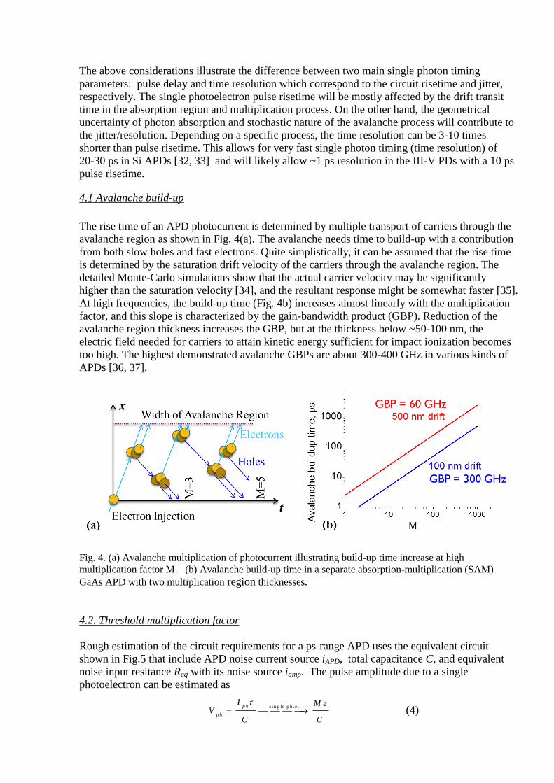
4.1 Avalanche build-up
The rise time of an APD photocurrent is determined by multiple transport of carriers through the
avalanche region as shown in Fig. 4(a). The avalanche needs time to build-up with a contribution
from both slow holes and fast electrons. Quite simplistically, it can be assumed that the rise time
is determined by the saturation drift velocity of the carriers through the avalanche region. The
detailed Monte-Carlo simulations show that the actual carrier velocity may be significantly
higher than the saturation velocity [34], and the resultant response might be somewhat faster [35].
At high frequencies, the build-up time (Fig. 4b) increases almost linearly with the multiplication
factor, and this slope is characterized by the gain-bandwidth product (GBP). Reduction of the
avalanche region thickness increases the GBP, but at the thickness below ~50-100 nm, the
electric field needed for carriers to attain kinetic energy sufficient for impact ionization becomes
too high. The highest demonstrated avalanche GBPs are about 300-400 GHz in various kinds of
APDs [36, 37].
Fig. 4. (a) Avalanche multiplication of photocurrent illustrating build-up time increase at high
multiplication factor M. (b) Avalanche build-up time in a separate absorption-multiplication (SAM)
GaAs APD with two multiplication region thicknesses.
4.2. Threshold multiplication factor
Rough estimation of the circuit requirements for a ps-range APD uses the equivalent circuit
shown in Fig.5 that include APD noise current source iAPD, total capacitance C, and equivalent
noise input resitance Req with its noise source iamp. The pulse amplitude due to a single
photoelectron can be estimated as
(4)
s in g le p h .e .p h
p h
I M eV
C C
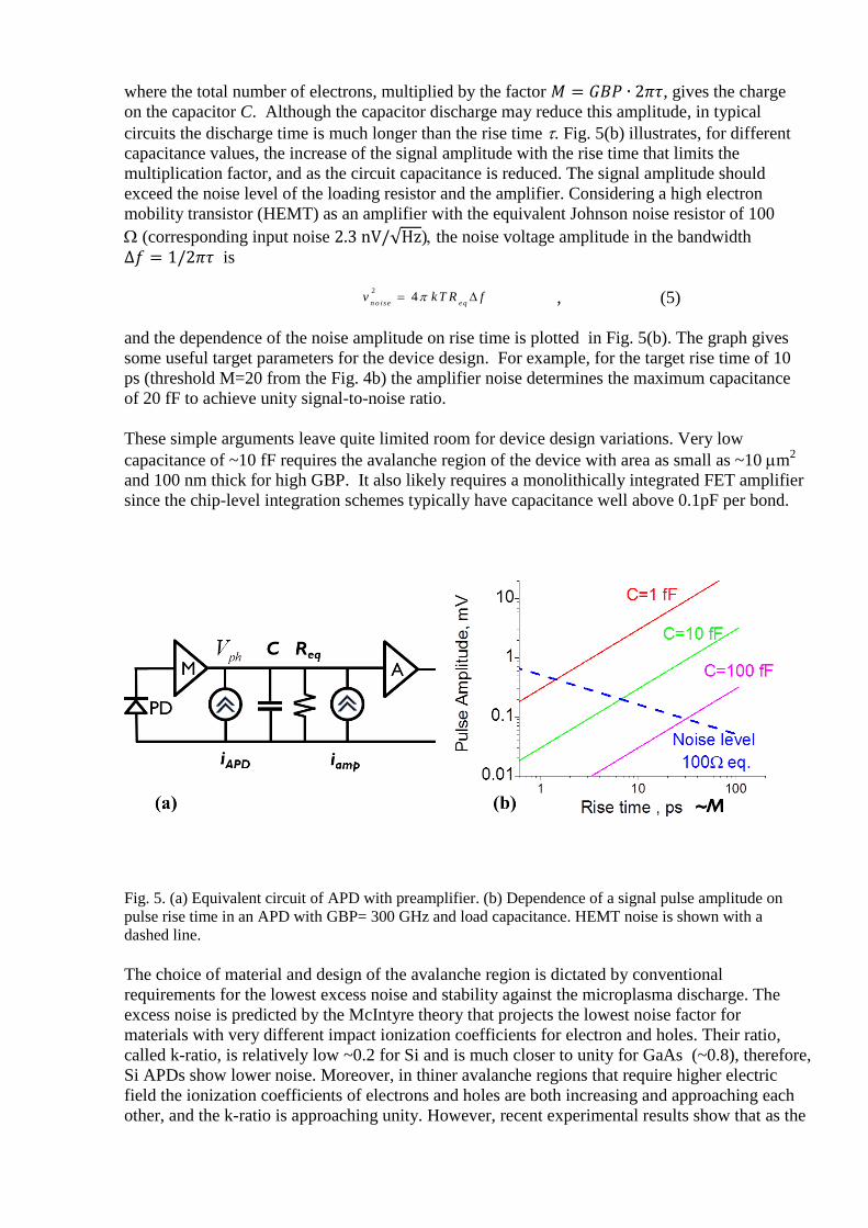
where the total number of electrons, multiplied by the factor , gives the charge
on the capacitor C. Although the capacitor discharge may reduce this amplitude, in typical
circuits the discharge time is much longer than the rise time . Fig. 5(b) illustrates, for different
capacitance values, the increase of the signal amplitude with the rise time that limits the
multiplication factor, and as the circuit capacitance is reduced. The signal amplitude should
exceed the noise level of the loading resistor and the amplifier. Considering a high electron
mobility transistor (HEMT) as an amplifier with the equivalent Johnson noise resistor of 100
(corresponding input noise √ ) the noise voltage amplitude in the bandwidth
is
, (5)
and the dependence of the noise amplitude on rise time is plotted in Fig. 5(b). The graph gives
some useful target parameters for the device design. For example, for the target rise time of 10
ps (threshold M=20 from the Fig. 4b) the amplifier noise determines the maximum capacitance
of 20 fF to achieve unity signal-to-noise ratio.
These simple arguments leave quite limited room for device design variations. Very low
capacitance of ~10 fF requires the avalanche region of the device with area as small as ~10 m2
and 100 nm thick for high GBP. It also likely requires a monolithically integrated FET amplifier
since the chip-level integration schemes typically have capacitance well above 0.1pF per bond.
Fig. 5. (a) Equivalent circuit of APD with preamplifier. (b) Dependence of a signal pulse amplitude on
pulse rise time in an APD with GBP= 300 GHz and load capacitance. HEMT noise is shown with a
dashed line.
The choice of material and design of the avalanche region is dictated by conventional
requirements for the lowest excess noise and stability against the microplasma discharge. The
excess noise is predicted by the McIntyre theory that projects the lowest noise factor for
materials with very different impact ionization coefficients for electron and holes. Their ratio,
called k-ratio, is relatively low ~0.2 for Si and is much closer to unity for GaAs (~0.8), therefore,
Si APDs show lower noise. Moreover, in thiner avalanche regions that require higher electric
field the ionization coefficients of electrons and holes are both increasing and approaching each
other, and the k-ratio is approaching unity. However, recent experimental results show that as the
24
n o is e e qv k T R f
avalanche region becomes thinner the excess noise is decreasing instead of increasing [38].
Even more promising are the continuing efforts to engineer impact ionization region using
multilayer III-V structures [39-41]. This approach results in an increase of the kinetic energy of
injected electrons and better localization of the impact-ionization events; as a result a very low
excess noise factor of 3.3 at M=16 in a thin 260 nm wide bandgap Al0.6Ga0.4As multiplication
region was demonstrated [42].
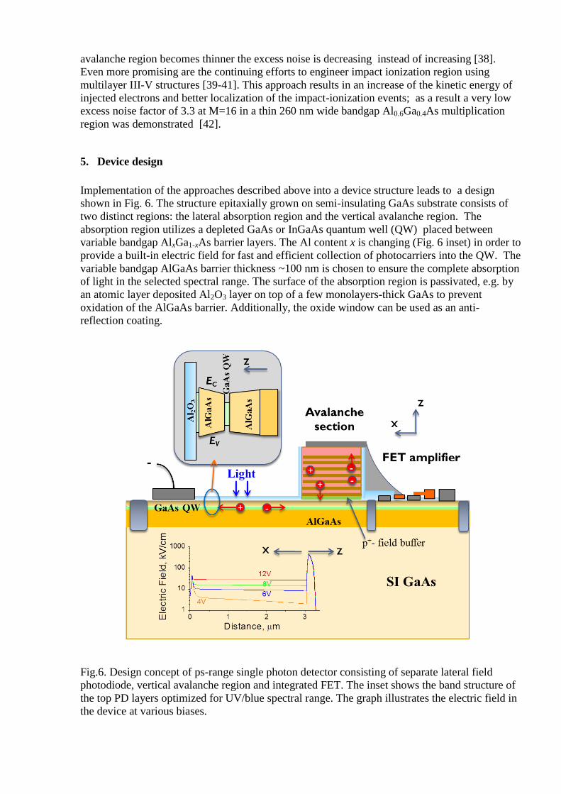
5. Device design
Implementation of the approaches described above into a device structure leads to a design
shown in Fig. 6. The structure epitaxially grown on semi-insulating GaAs substrate consists of
two distinct regions: the lateral absorption region and the vertical avalanche region. The
absorption region utilizes a depleted GaAs or InGaAs quantum well (QW) placed between
variable bandgap AlxGa1-xAs barrier layers. The Al content x is changing (Fig. 6 inset) in order to
provide a built-in electric field for fast and efficient collection of photocarriers into the QW. The
variable bandgap AlGaAs barrier thickness ~100 nm is chosen to ensure the complete absorption
of light in the selected spectral range. The surface of the absorption region is passivated, e.g. by
an atomic layer deposited Al2O3 layer on top of a few monolayers-thick GaAs to prevent
oxidation of the AlGaAs barrier. Additionally, the oxide window can be used as an anti-
reflection coating.
Fig.6. Design concept of ps-range single photon detector consisting of separate lateral field
photodiode, vertical avalanche region and integrated FET. The inset shows the band structure of
the top PD layers optimized for UV/blue spectral range. The graph illustrates the electric field in
the device at various biases.
The left contact in Fig. 6 could utilize either epitaxial p+-GaAs junction or Schottky barrier with
a high work-function metal that create minimal intermetallics with GaAs, such as Pt or Ti. These
types of contacts have large barriers for electron injection and will minimize the dark current
associated with contacts. The generation/recombination current in the absorption region is
minimized by a relatively small volume of the device and reduced surface recombination due to
the adequate passivation layer.
Due to orthogonal fields, the absorption and the avalanche regions can have different cross-
section areas. As the avalanche region should be thin (<100nm) to provide fast multiplication
build-up, its cross-section should be minimized to give low capacitance. A p+-field buffer
separates the undoped absorption region with relatively low electric field ~10 kV/cm and
avalanche region with the field >400kV/cm. The field distribution is also shown in the inset of
Fig.6. The avalanche region will likely employ AlGaAs or superlattice multiplication structure
as discussed above. Although there are significant technological challenges, such as reduced
defect density, surface leakage and isolation, avalanche stability against microplasma
discharge/breakdown, which need to be dealt with, there are no physical reasons preventing this
device from operating as expected.
6. Device integration
As described above, one of the major limiting factors of the fast PDs is their capacitance which
proportionally reduces the pulse amplitude. As a result, faster detection of weak signals requires
smaller area PDs. The fastest silicon avalanche PDs of 10 m diameter can detect photon arrival
time with resolutions down to 30-40 ps or even 20 ps for 5 m PD [32, 33].
Since many applications need large area detectors, the capacitance is reduced by partitioning of
the photodetector area into array of small pixels. PDs with analog summation of signals from the
individual pixels are available from Hamamatsu, RMD and others, digital circuits have been
recently implemented by Philips [23, 24].These “Si photomultipliers” (SiPMTs) are becoming
now a standard for single photon detectors. Although the partitioning of large area (mm and cm
size) detectors is inevitable for ps-range detectors, the partitioning size requirement can be
substantially relaxed in case of PDs with lateral field.
As illustrated in the Figs. 1 and 5(b), a lateral field GaAs pixel with 30x30 m2 size will have a
capacitance of 10 fF, good enough to obtain a measurable 10 ps intrinsic single photoelectron
response. However, to utilize this short risetime, the input and parasitic capacitances of an
amplifier should be also less than 10 fF. This requirement is relatively easy to meet in monolithic
integrated circuits, but before the full-scale III-V digital circuits evolve it is likely that the PD
array will have to be integrated with a silicon read-out chip containing active quenching and
gating circuits [7]. Most of the chip area array interconnection technologies operate with
relatively large, 10’s of micrometers in size, interconnects (solder bumps, bridges, and filled
vias) with a capacitance exceeding 100 fF per bond. To accommodate this large parasitic
capacitance, the APD output is routed to on-chip FET for further amplification. An amplifier,
such as a high electron mobility transistor (HEMT) or MOSFET should be placed in a close
vicinity to the PD pixel (Fig.6). Lateral field PD geometry is well-suited for monolithic
integration with field-effect transistors as they both utilize similar basic technologies. In addition,
the FET in Fig.6 can use the same epitaxial QW layer structure for the channel as for the PD
absorber.
The integration of MSM PD with MESFETs and HEMTs has been established for a long time [6,
43, 44]. However, the advancements in the group III-V semiconductor technology have only
recently resulted in high-performance MOSFETs and other 3-dimensional FETs that overcome
performance of Si-based transistors, and are compatible with the design in Fig. 6.
One of the long-standing challenges in III-V FETs is the semiconductor surface passivation. The
latest advances in gate oxide technologies for MOSFETs made interfaces with low interface rap
densities possible. Surface passivation techniques include deposition of Ga2O3(Gd2O3) [45],
ultrathin amorphous silicon passivation layer [46], or atomic layer deposition od Al2O3 with self-
cleaning effect of TMA (Trimethylaluminium) precursor [47]. It is important that the interfaces
with low density of interface traps (1011
-1012
cm-3
eV-1
) also demonstrated low surface
recombination rates [48]. Combined with the surface band engineering to separate the
photocarriers from the oxide interface with wide-bandgap semiconductor (Fig. 6), the passivation
layer can drastically reduce the surface state density. Given that the oxides (Al2O3, SiO2, HfO2)
are large bandgap materials, they can be used as UV/visible windows protecting detector from
the environment as well as an anti-reflection coating.
Based on the previous discussion, Table III summarizes how the materials and device parameters
affect the characteristics of the PD. It is worth noting that the proposed device geometry allows
for the best combination of large absorption area, short absorption length essential for blue/UV
spectral range, low capacitance of both absorption region (due to the lateral field ) and avalanche
region (due to low cross-section) if high mobility/ high saturation velocity material is used.
Table III. Effect of material parameters and device design on characteristics of a UV PD with
lateral field
PD characteristics Material and design parameters
UV Efficiency
- Surface recombination
- Band structure of the absorption
region
- Avalanche initiation probability
Delay/latency
- Device capacitance
- Drift time in absorption region
- Avalanche build-up
Jitter/ time
resolution
- Avalanche build-up
- Drift time in absorption region
- Device capacitance
Dark current/noise
count rate
- Injection from contacts
- Surface generation/recombination
- Bulk generation/recombination in
absorption and avalanche regions
Amplitude of a
single photoelectron
pulse
- Device and integration capacitance
- Avalanche multiplication
Lastly, an area array integration with Si electronics is required to achieve functionality similar to
SiPMT photodetector, including discriminating, active quenching, gating and/or time correlation
circuits. Depending upon the scale, complexity and functionality of the detector, one can
envision well-established varieties of flip-chip integration with solder bumps used, for example,
for bonding focal plane arrays on silicon. More recently developed 3D integration technologies
with wafer bonding and interconnecting through-wafer via holes could also be used.
Summary
We proposed a novel design of an ultrafast single photon photodetector for UV/visible spectral
range and picosecond-level timing resolution. The detector has separate absorption and
amplification regions. The absorption region, covering large fraction of the total device area, has
lateral electric field while the low area and low capacitance avalanche region has the field
electric field normal to the substrate plane. The design rules and requirements are analyzed
against demonstrated devices and technologies.
References
[1] V. Boccone, P.K. Lightfoot, K. Mavrokoridis, C. Regenfus, C. Amsler, A. Badertscher, A. Bueno, H. Cabrera, M.C. Carmona-Benitez, M. Daniel, E.J. Daw, U. Degunda, A. Dell'Antone, A. Gendotti, L. Epprecht, S. Horikawa, L. Kaufmann, L. Knecht, M. Laffranchi, C. Lazzaro, D. Lussi, J. Lozano, A. Marchionni, A. Melgarejo, P. Mijakowski, G. Natterer, S. Navas-Concha, P. Otyugova, M. de Prado, P. Przewlocki, F. Resnati, M. Robinson, J. Rochet, L. Romero, E. Rondio, A. Rubbia, N.J.C. Spooner, T. Strauss, J. Ulbricht, T. Viant, Development of wavelength shifter coated reflectors for the ArDM argon dark matter detector, Journal of Instrumentation, 4 (2009) P06001.
[2] S. White, Experimental Challenges of the European Strategy for Particle Physics, Proc. CHEF, 2013 (arXiv:1309.7985 [physics.ins-det] ).
[3] P.A. Scowen, M.R. Perez, S.G. Neff, D.J. Benford, Scientific Objectives for UV/Visible Astrophysics Investigations: A Summary of Responses by the Community (2012), 2013 (arXiv:1306.0553 [astro-ph.IM]).
[4] R.W. Novotny, Fast inorganic scintillators - status and outlook, Journal of Physics: Conference Series, 443 (2013) 012080.
[5] M. Conti, L. Eriksson, H. Rothfuss, C.L. Melcher, Comparison of fast scintillators with TOF PET potential, IEEE Transactions on Nuclear Science, 56 (2009) 926.
[6] K. Kato, Ultrawide-band/high-frequency photodetectors, IEEE Transactions on Microwave Theory and Techniques, 47 (1999) 1265.
[7] S. Cova, M. Ghioni, A. Lotito, I. Rech, F. Zappa, Evolution and prospects for single-photon avalanche diodes and quenching circuits, Journal of Modern Optics, 51 (2004) 1267.
[8] I. Prochazka, Semiconducting single photon detectors: the state of the art, Physica Status Solidi C, (2005) 1524.
[9] M. Itzler, J. Xudong, M. Entwistle, K. Slomkowski, A. Tosi, F. Acerbi, F. Zappa, S. Cova, Advances in InGaAsP-based avalanche diode single photon detectors, Journal of Modern Optics, 58 (2011) 174.
[10] S.Y. Chou, Y. Liu, W. Khalil, T.Y. Hsiang, S. Alexandrou, Ultrafast nanoscale metal-semiconductor-metal photodetectors on bulk and low-temperature grown GaAs, Applied Physics Letters, 61 (1992) 819.
[11] E.M. Gallo, A. Cola, F. Quaranta, J.E. Spanier, High speed photodetectors based on a two-dimensional electron/hole gas heterostructure, Applied Physics Letters, 102 (2013) 161108.
[12] S.E. Ralph, M.C. Hargis, G.D. Pettit, Large area, low voltage, transit time limited InGaAs metal semiconductor metal photodetectors, Applied Physics Letters, 61 (1992) 2222.
[13] B.J. Van Zeghbroeck, W. Patrick, J.M. Halbout, P. Vettiger, 105-GHz bandwidth metal-semiconductor-metal photodiode, IEEE Electron Device Letters, 9 (1988) 527.
[14] J.B.D. Soole, H. Schumacher, InGaAs metal-semiconductor-metal photodetectors for long wavelength optical communications, IEEE Journal of Quantum Electronics, 27 (1991) 737.
[15] J.C. Carrano, T. Li, D.L. Brown, P.A. Grudowski, C.J. Eiting, R.D. Dupuis, J.C. Campbell, Very high-speed metal-semiconductor-metal ultraviolet photodetectors fabricated on GaN, Applied Physics Letters, 73 (1998) 2405.
[16] J. Li, Y. Xu, T.Y. Hsiang, W.R. Donaldson, Picosecond response of gallium-nitride metal–semiconductor–metal photodetectors, Applied Physics Letters, 84 (2004) 2091.
[17] E.H. Bottcher, F. Hieronymi, D. Kuhl, E. Droge, D. Bimberg, Transient response of lateral photodetectors, Applied Physics Letters, 62 (1993) 2227.
[18] M. Razeghi, A. Rogalski, Semiconductor ultraviolet detectors, Journal of Applied Physics, 79 (1996) 7433.
[19] S. Nikzad, M.E. Hoenk, P.J. Grunthaner, R.W. Terhune, F.J. Grunthaner, R. Winzenread, M.M. Fattahi, H.-F. Tseng, M.P. Lesser, Delta-doped CCDs: high QE with long-term stability at UV and visible wavelengths, Proceedings of the SPIE, 2198 (1994) 907.
[20] S. Nikzad, M.E. Hoenk, F. Greer, B. Jacquot, S. Monacos, T.J. Jones, J. Blacksberg, E. Hamden, D. Schiminovich, C. Martin, P. Morrissey, Delta-doped electron-multiplied CCD with absolute quantum efficiency over 50% in the near to far ultraviolet range for single photon counting applications, Applied Optics, 51 (2012) 365.
[21] S. Oktyabrsky, Y. Nishi, S. Koveshnikov, W.-E. Wang, N. Goel, W. Tsai, Materials and Technologies for III-V MOSFETs, in: S. Oktyabrsky, P. Ye (Eds.) Fundamentals of III-V Semiconductor MOSFETs, Springer US, 2010, p. 195.
[22] M. Ito, O. Wada, Low dark current GaAs metal-semiconductor-metal (MSM) photodiodes using WSix contacts, IEEE Journal of Quantum Electronics, QE-22 (1986) 1073.
[23] S.-W. Seo, S.-Y. Cho, S. Huang, J.J. Shin, N.M. Jokerst, A.S. Brown, M.A. Brooke, High-speed large-area inverted InGaAs thin-film metal-semiconductor-metal photodetectors, IEEE Journal of Selected Topics in Quantum Electronics, 10 (2004) 686.
[24] C.-T. Lee, H.-Y. Lee, Metal-semiconductor-metal photodetectors with InAlGaP capping and buffer layers, IEEE Electron Device Letters, 24 (2003) 532.
[25] R.-H. Yuang, J.-L. Shieh, R.-M. Lin, J.-I. Chyi, GaAs metal-semiconductor-metal photodetectors (MSM-PD'S) with AlGaAs cap and buffer layers, Journal of the Chinese Institute of Engineers, 18 (1995) 445.
[26] J. Kim, W.B. Johnson, S. Kanakaraju, L.C. Calhoun, C.H. Lee, Improvement of dark current using InP/InGaAsP transition layer in large-area InGaAs MSM photodetectors, IEEE Transactions on Electron Devices, 51 (2004) 351.
[27] X. Chen, B. Nabet, A. Cola, F. Quaranta, M. Currie, An AlGaAs-GaAs-based RCE MSM photodetector with delta modulation doping, IEEE Electron Device Letters, 24 (2003) 312.
[28] Kyosemi, KPDG020C, 2014 (http://kyosemi.co.jp/en/communication/gaas_photodiode/kpdg020c).
[29] Hamamatsu, SI227 PD, 2014 (http://www.hamamatsu.com/us/en/product/category/3100/4001/4103/S1227-1010BQ/index.html).
[30] H. Chen, L. Jiang, X. Chen, Design optimization of GaAs Betavoltaic batteries, Journal of Physics D: Applied Physics, 44 (2011) 215303.
[31] J.C. Campbell, S. Demiguel, M. Feng, A. Beck, G. Xiangyi, W. Shuling, Z. Xiaoguang, L. Xiaowei, J.D. Beck, M.A. Kinch, A. Huntington, L.A. Coldren, J. Decobert, N. Tscherptner, Recent advances in avalanche photodiodes, IEEE Journal of Selected Topics in Quantum Electronics, 10 (2004) 777.
[32] A. Lacaita, S. Cova, M. Ghioni, F. Zappa, Single-photon avalanche diode with ultrafast pulse response free from slow tails, IEEE Electron Device Letters 14 (1993) 360.
[33] A. Spinelli, M.A. Ghioni, S.D. Cova, L.M. Davis, Avalanche detector with ultraclean response for time-resolved photon counting, IEEE Journal of Quantum Electronics 34 (1998) 817.
[34] S.A. Plimmer, J.P.R. David, B. Jacob, G.J. Rees, Impact ionization probabilities as functions of two-dimensional space and time, Journal of Applied Physics, 89 (2001) 2742.
[35] M.M. Hayat, K. Oh-Hyun, P. Yi, P. Sotirelis, J.C. Campbell, B.E.A. Saleh, M.C. Teich, Gain-bandwidth characteristics of thin avalanche photodiodes, IEEE Transactions on Electron Devices, 49 (2002) 770.
[36] G.S. Kinsey, R. Sidhu, A.L. Holmes, Jr., J.C. Campbell, A.G. Dentai, High-speed waveguide avalanche photodetectors, Device Research Conference Digest 2001, pp. 149.
[37] Y. Kang, H.-D. Liu, M. Morse, M.J. Paniccia, M. Zadka, S. Litski, G. Sarid, A. Pauchard, Y.-H. Kuo, H.-W. Chen, W.S. Zaoui, J.E. Bowers, A. Beling, D.C. McIntosh, X. Zheng, J.C. Campbell, Monolithic germanium/silicon avalanche photodiodes with 340 GHz gain-bandwidth product, Nature Photonics, 3 (2009) 59.
[38] C. Hu, K.A. Anselm, B.G. Streetman, J.C. Campbell, Noise characteristics of thin multiplication region GaAs avalanche photodiodes, Applied Physics Letters, 69 (1996) 3734.
[39] P. Yuan, S. Wang, X. Sun, X.G. Zheng, A.L. Holmes, Jr., J.C. Campbell, Avalanche photodiodes with an impact-ionization-engineered multiplication region, IEEE Photonics Technology Letters, 12 (2000) 1370.
[40] O.-H. Kwon, M.M. Hayat, W. Shuling, J.C. Campbell, A. Holmes, Jr., P. Yi, B.E.A. Saleh, M.C. Teich, Optimal excess noise reduction in thin heterojunction Al0.6Ga0.4As-GaAs avalanche photodiodes, IEEE Journal of Quantum Electronics, 39 (2003) 1287.
[41] S. Wenlu, Z. Xiaoguang, L. Zhiwen, J.C. Campbell, Monte Carlo Simulation of InAlAs/InAlGaAs Tandem Avalanche Photodiodes, IEEE Journal of Quantum Electronics, 48 (2012) 528.
[42] C.H. Tan, J.P.R. David, S.A. Plimmer, G.J. Rees, R.C. Tozer, R. Grey, Low multiplication noise thin Al0.6Ga0.4As avalanche photodiodes, IEEE Transactions on Electron Devices, 48 (2001) 1310.
[43] M. Ito, T. Kumai, H. Hamaguchi, M. Makiuchi, K. Nakai, O. Wada, T. Sakurai, High‐speed
monolithically integrated GaAs photoreceiver using a metal‐semiconductor‐metal
photodiode, Applied Physics Letters, 47 (1985) 1129. [44] P. Fay, C. Caneau, I. Adesida, High-speed MSM/HEMT and p-i-n/HEMT monolithic
photoreceivers, IEEE Transactions on Microwave Theory and Techniques, 50 (2002) 62. [45] J. Kwo, D.W. Murphy, M. Hong, R.L. Opila, J.P. Mannaerts, A.M. Sergent, R.L. Masaitis,
Passivation of GaAs using (Ga2O3)1-x(Gd2O3)x, 0<x<1.0 films, Applied Physics Letters, 75 (1999) 1116.
[46] S. Oktyabrsky, V. Tokranov, M. Yakimov, R. Moore, S. Koveshnikov, W. Tsai, F. Zhu, J.C. Lee, High-k gate stack on GaAs and InGaAs using in situ passivation with amorphous silicon, Materials Science & Engineering B 135 (2006) 272.
[47] W. Wang, C.L. Hinkle, E.M. Vogel, K. Cho, R.M. Wallace, Is interfacial chemistry correlated to gap states for high-k/III-V interfaces?, Microelectronic Engineering, 88 (2011) 1061.
[48] M. Passlack, R. Droopad, Z. Yu, N. Medendorp, D. Braddock, X.W. Wang, T.P. Ma, T. Buyuklimanli, Screening of oxide/GaAs interfaces for MOSFET applications, IEEE Electron Device Letters, 29 (2008) 1181.