Embed Size (px)
Citation preview

Piezoresistive Strain Gauges for use in Wireless Component Monitoring Systems
Stephen P. Olson1, Dr. James Castracane1, Ryk E. Spoor2
1 ll f l i d i i i i lb i i1College of Nanoscale Science and Engineering, University at Albany, State University of New York, 255 Fuller Road, Albany, NY 12203, Email: [email protected],
[email protected] Electronic Machines Corporation (IEM). 60 Fourth Avenue, Albany, NY
12202, Email: [email protected]
cnse.albany.edu
, p @

Outline
•Strain monitoring systems for rotating helicopter parts
•Strain gauge requirements – Low power consumption
•Piezoresistive strain gauges
S i d i d f b i i fl•Strain gauge design and fabrication flow
•Test setup
•Strain response simulation
•Strain gauge measurements - Response and noiseStrain gauge measurements Response and noise
•Conclusions and acknowledgements
cnse.albany.edu

Overall Goal:
Component monitoring
Reduce unnecessary prescribed maintenance schedules by providing real-time data on component condition.
• Pitch link controls the angle of the rotor blade as it spins• One of many parts critical for controlled flightOne of many parts critical for controlled flight• Currently these parts are replaced based on usage hours
• Expensive• Condition is not known while in serviceCondition is not known while in service
Wireless strain monitoring tagsP t• Power system
• Data gathering and signal conditioning• RF transmitter• Strain gaugeg g
• Wireless system and properties of the pitch link place unique requirements on the strain gauge
• The focus of this project is to design, fabricate and
cnse.albany.edu
e ocus o t s p oject s to des g , ab cate a dpackage strain gauge devices for this system
Strain gauge requirements
C T G R ( h ) SiCompany Type G R (ohm) SizeOmega Metal foil 2 120 5x6mmSoltec Corporation Semiconductor -100 120 11mm diaMicron Semiconductor 100..155 540..1050 10.6x3
Requirements for the sensor:M lti i
Omega1Soltec2 Micron3
• Multi-axis• Power consumption <100µW, preferably 10µW• 5 µε resolution, 10 kHz measurement bandwidth• Small size, target size for entire tag is 12.7mm square (sensor, power system, readout
1. www.omega.com/pptst/Rosettes Stackedgrid Strain SG.html
, g g q ( , p y ,electronics and RF transmitter)
• Low power requires a large gauge factor (sensitivity), large resistance (~100kΩ) • Operational temperature range -20 to 70 ºC
cnse.albany.edu
1. www.omega.com/pptst/Rosettes_Stackedgrid_Strain_SG.html2. www.solteccorp.com/products.aspx?catid=48 3. www.microninstruments.com/products/gages/ssgh-halfbackgage.htm
Resistive strain gauges
• Conductors change resistance when strainedlR ρ= ( )L
LRR G ΔΔ =
• Conductors change resistance when strained• Gauge factor is the sensitivity of the gauge
• Resistance of a wire is proportional to its length• Poisson ratio reduces the cross-sectional area
AR =
lΔl
A Poisson ratio reduces the cross sectional area, increasing the resistance
• Piezoresistive materials change resistivity when a stress is applied, changing the resistance of the gauge
EG lπν ++= 21 <110>
<100>
110
For a strain gauge with a rectangular cross section
Longitudinal Transverse
~2 >100
cross sectionG Gauge FactorE Young’s modulusν Poisson ratioπ Piezoresistive coefficient
10-11 Pa -1-110
cnse.albany.edu
πl Piezoresistive coefficientP-type Silicon piezoresistance coefficients
Marc J. Madou, Fundamentals of Microfabrication: The Science of Miniaturization, CRC; 2 edition (March 13, 2002)
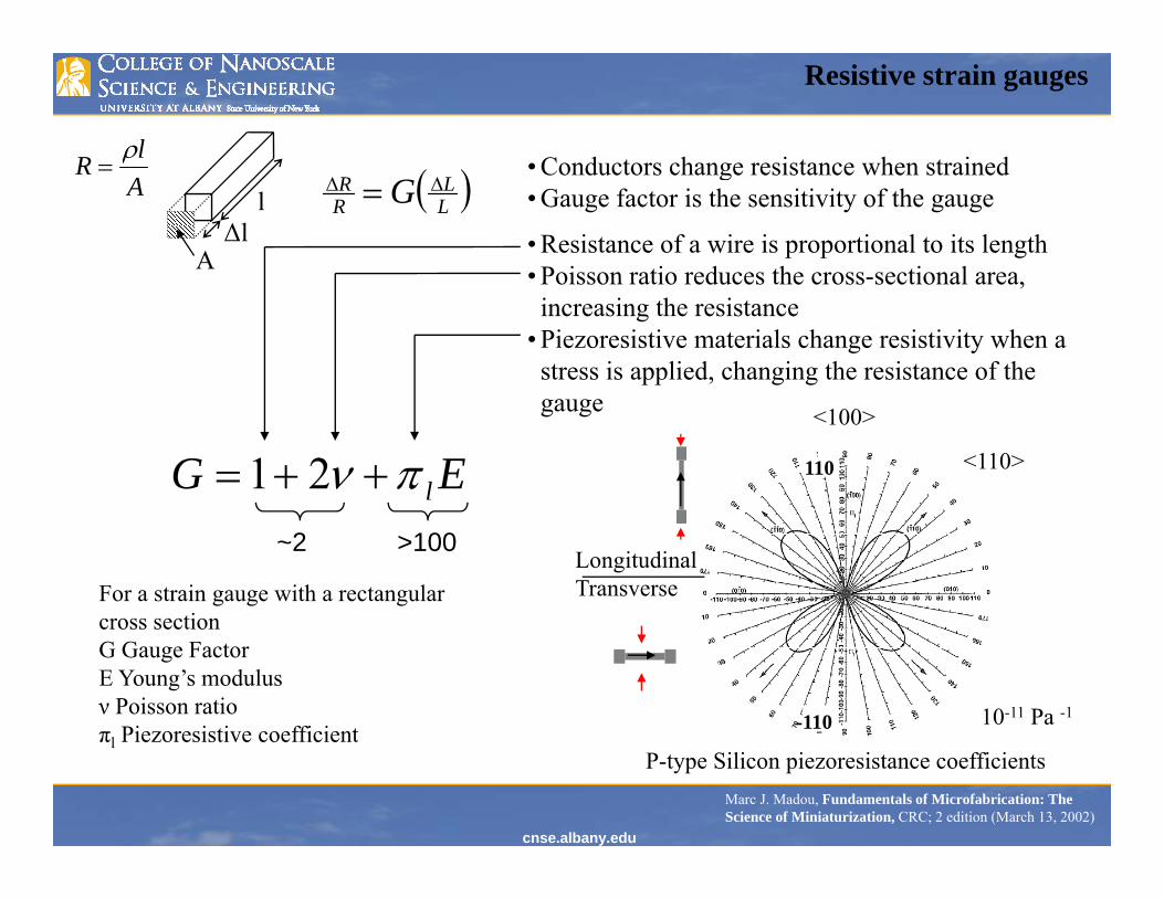
Noise sources
N i ill li it l ti•Noise will limit sensor resolution•Johnson or thermal noise
• Frequency independent• Depends on resistance temperature and measurementDepends on resistance, temperature and measurement
bandwidth• kB Boltzmann's constant• R=100kΩ, T=300K, measurement bandwidth=10kHz
RMSBThermal VffTRkV 6minmax 102)( −×=−=
•1/f noise• Frequency dependentq y p• Hooge noise model depends on the number of carriers, bias
voltage, and measurement frequency• N= 9x10⁸, α=1x10⁻⁵, Vb =1V, fmax/fmin=10,000
RMSb
f Vff
NVV 7
min
max2
/1 102.3ln −×=⎟⎟⎠
⎞⎜⎜⎝
⎛=
α
cnse.albany.edu
Harkey, J.A. Kenny, T.W, Journal of microelectromechanical systems, 9 no. 2 2000
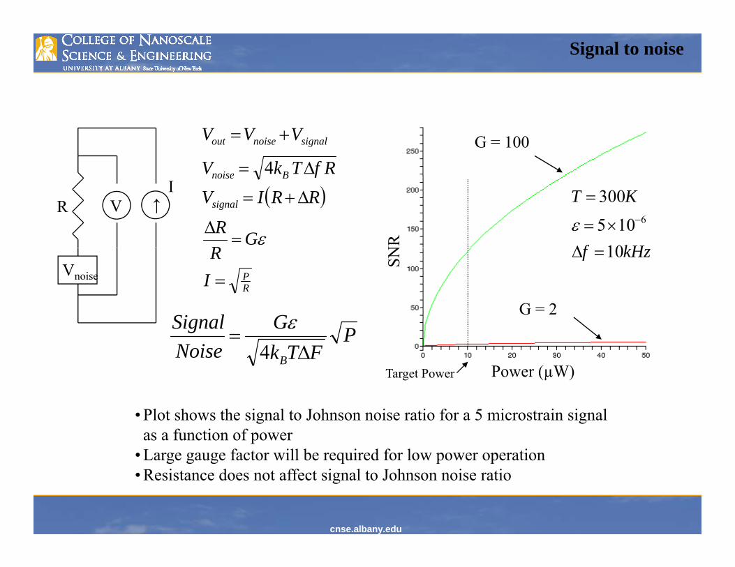
Signal to noise
Bnoise
signalnoiseout
RfTkV
VVV
Δ=
+=
4G = 100
( )signal
Bnoise
GRR
RRIVf
=Δ
Δ+=
ε
↑VI
R
NR kHf
KT
10105
3006
Δ×=
=−ε
RPI
R=
GSi l ε
Vnoise
SN
G = 2
kHzf 10=Δ
PFTk
GNoiseSignal
B Δ=
4ε
Power (µW)Target Power
• Plot shows the signal to Johnson noise ratio for a 5 microstrain signal as a function of power
• Large gauge factor will be required for low power operation
cnse.albany.edu
g g g q p p• Resistance does not affect signal to Johnson noise ratio
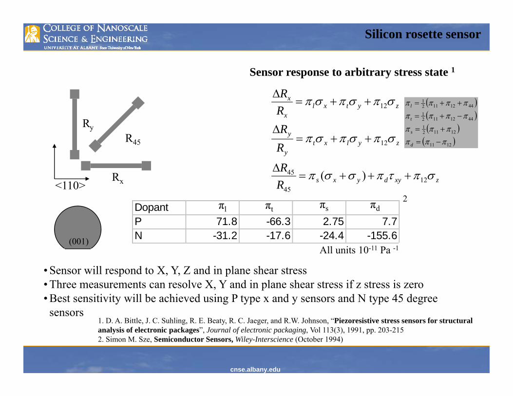
Silicon rosette sensor
Sensor response to arbitrary stress state 1
zytxlx
x
RR σπσπσπ 12++=
Δ
R
( )( )4412112
1
44121121
ππππππππ
−+=
++=
t
l
Sensor response to arbitrary stress state
zylxty
y
R
RR
σπσπσπ
45
12
)( +++Δ
++=ΔRy
R
R45
( )( )1211
121121
ππππππ
−=
+=
d
s
zxydyxsRσπτπσσπ 12
45
45 )( +++=Rx<110>
DopantP 71 8 -66 3 2 75 7 7
2πl πt πs πd
P 71.8 66.3 2.75 7.7N -31.2 -17.6 -24.4 -155.6
• Sensor will respond to X, Y, Z and in plane shear stress
All units 10-11 Pa -1(001)
Sensor will respond to X, Y, Z and in plane shear stress• Three measurements can resolve X, Y and in plane shear stress if z stress is zero• Best sensitivity will be achieved using P type x and y sensors and N type 45 degree
sensors1. D. A. Bittle, J. C. Suhling, R. E. Beaty, R. C. Jaeger, and R.W. Johnson, “Piezoresistive stress sensors for structural
cnse.albany.edu
1. D. A. Bittle, J. C. Suhling, R. E. Beaty, R. C. Jaeger, and R.W. Johnson, Piezoresistive stress sensors for structural analysis of electronic packages”, Journal of electronic packaging, Vol 113(3), 1991, pp. 203-2152. Simon M. Sze, Semiconductor Sensors, Wiley-Interscience (October 1994)
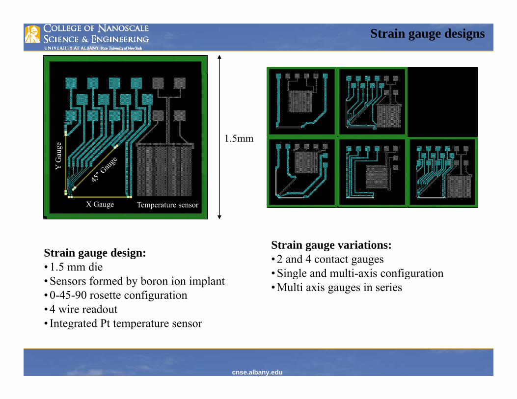
Strain gauge designs
1.5mm
Y G
auge
Temperature sensorX Gauge
Strain gauge variations:• 2 and 4 contact gauges• Single and multi-axis configuration
Strain gauge design:• 1.5 mm die Single and multi axis configuration
• Multi axis gauges in series• Sensors formed by boron ion implant• 0-45-90 rosette configuration• 4 wire readout• Integrated Pt temperature sensor
cnse.albany.edu
Integrated Pt temperature sensor
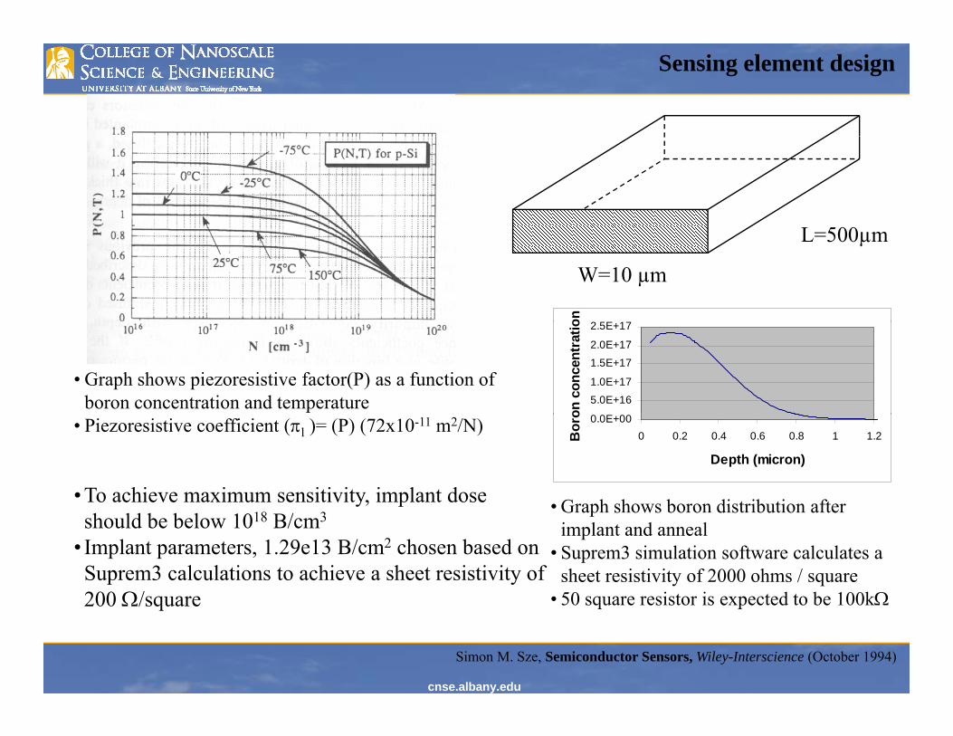
Sensing element design
L 500
W=10 µm
L=500µm
2 5E 17on
• Graph shows piezoresistive factor(P) as a function of boron concentration and temperature
0 0E 00
5.0E+16
1.0E+17
1.5E+17
2.0E+17
2.5E+17
on c
once
ntra
tio
• Piezoresistive coefficient (πl )= (P) (72x10-11 m2/N) 0.0E+000 0.2 0.4 0.6 0.8 1 1.2
Depth (micron)
Bor
o
• Graph shows boron distribution after• To achieve maximum sensitivity, implant dose • Graph shows boron distribution after implant and anneal
• Suprem3 simulation software calculates a sheet resistivity of 2000 ohms / square
• 50 square resistor is expected to be 100kΩ
should be below 1018 B/cm3
• Implant parameters, 1.29e13 B/cm2 chosen based on Suprem3 calculations to achieve a sheet resistivity of 200 Ω/square
cnse.albany.edu
Simon M. Sze, Semiconductor Sensors, Wiley-Interscience (October 1994)
• 50 square resistor is expected to be 100kΩ200 Ω/square
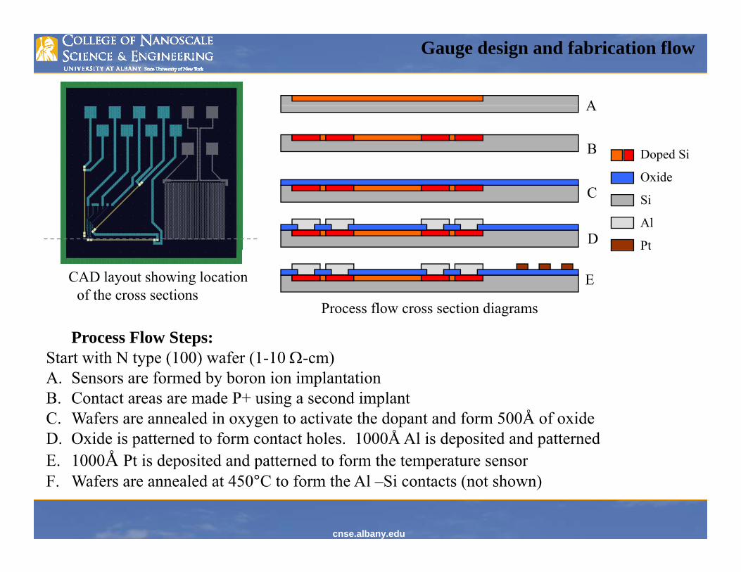
Gauge design and fabrication flow
AA
B Doped Si
OxideC
D
Oxide
Si
Al
Pt
CAD layout showing location of the cross sections
Process flow cross section diagrams
E
Process Flow Steps:Start with N type (100) wafer (1-10 Ω-cm)A. Sensors are formed by boron ion implantationB C t t d P+ i d i l tB. Contact areas are made P+ using a second implantC. Wafers are annealed in oxygen to activate the dopant and form 500Å of oxideD. Oxide is patterned to form contact holes. 1000Å Al is deposited and patternedE. 1000Å Pt is deposited and patterned to form the temperature sensor
cnse.albany.edu
p p pF. Wafers are annealed at 450°C to form the Al –Si contacts (not shown)
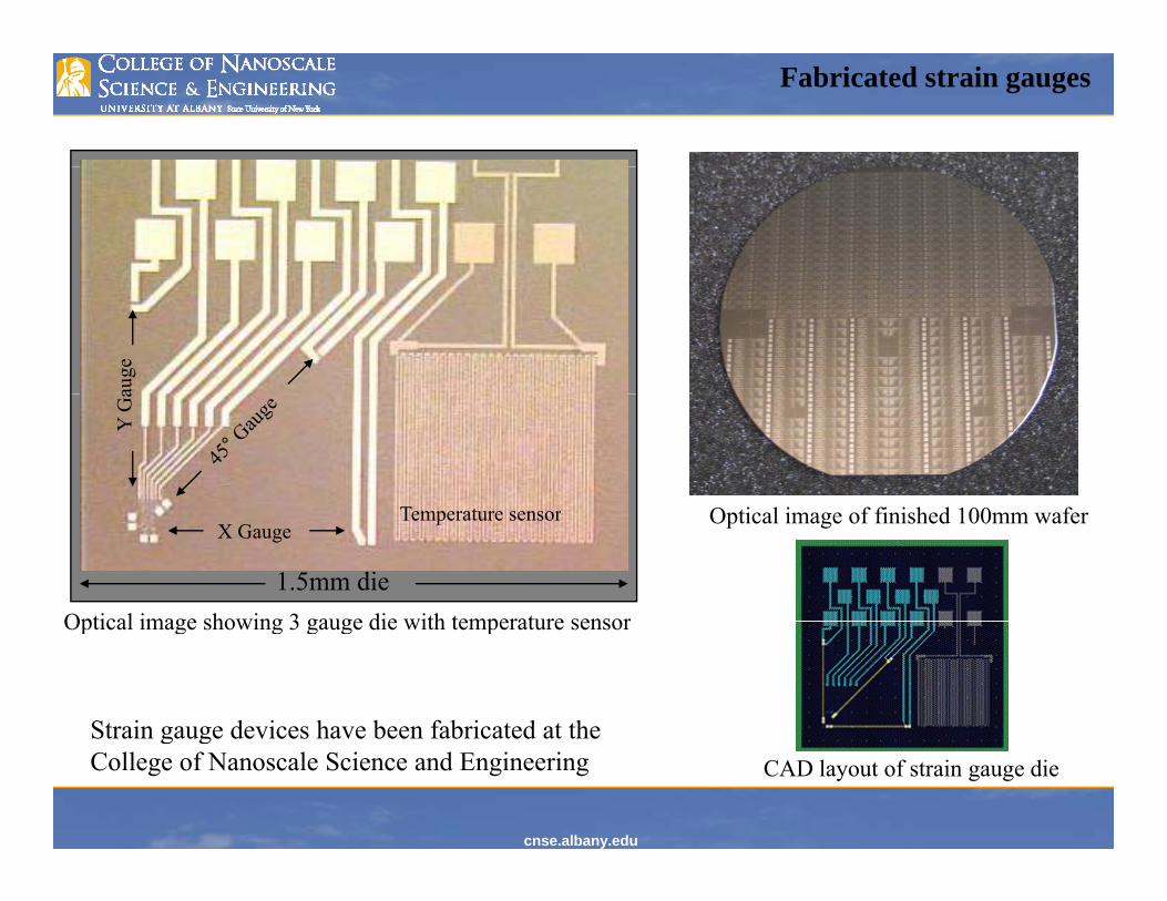
Fabricated strain gaugesau
ge
T
Y G
a
O i l i f fi i h d 100 fTemperature sensorX Gauge
1.5mm dieOptical image showing 3 gauge die with temperature sensor
Optical image of finished 100mm wafer
Optical image showing 3 gauge die with temperature sensor
Strain gauge devices have been fabricated at the
cnse.albany.edu
CAD layout of strain gauge dieStrain gauge devices have been fabricated at the College of Nanoscale Science and Engineering
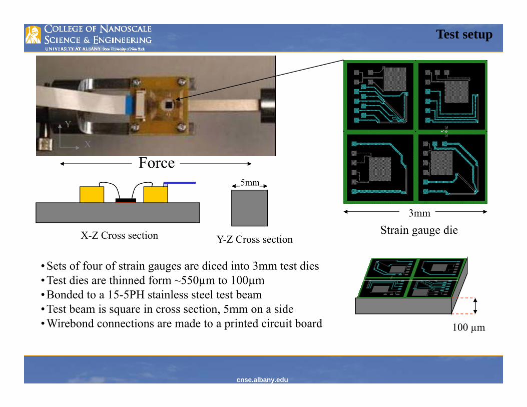
Test setup
Y
X
Y
Force
3mm
5mm
Strain gauge die
• Sets of four of strain gauges are diced into 3mm test dies• Test dies are thinned form ~550µm to 100µm
X-Z Cross section Y-Z Cross sectionStrain gauge die
• Test dies are thinned form ~550µm to 100µm• Bonded to a 15-5PH stainless steel test beam• Test beam is square in cross section, 5mm on a side• Wirebond connections are made to a printed circuit board 100 µm
cnse.albany.edu
µ
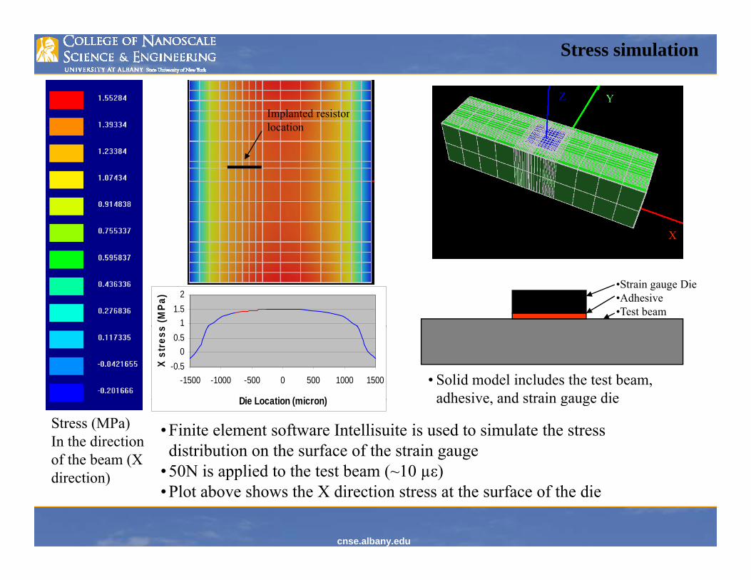
Stress simulation
YZImplanted resistorlocation
X
11.5
2
(MPa
)
•Strain gauge Die•Adhesive•Test beam
-0.50
0.5
-1500 -1000 -500 0 500 1000 1500
Die Location (micron)
X st
ress
• Solid model includes the test beam, adhesive and strain gauge die
Stress (MPa)In the direction of the beam (X di i )
• Finite element software Intellisuite is used to simulate the stress distribution on the surface of the strain gauge
• 50N is applied to the test beam (~10 µε)
Die Location (micron) adhesive, and strain gauge die
cnse.albany.edu
direction) 50N is applied to the test beam (~10 µε)• Plot above shows the X direction stress at the surface of the die
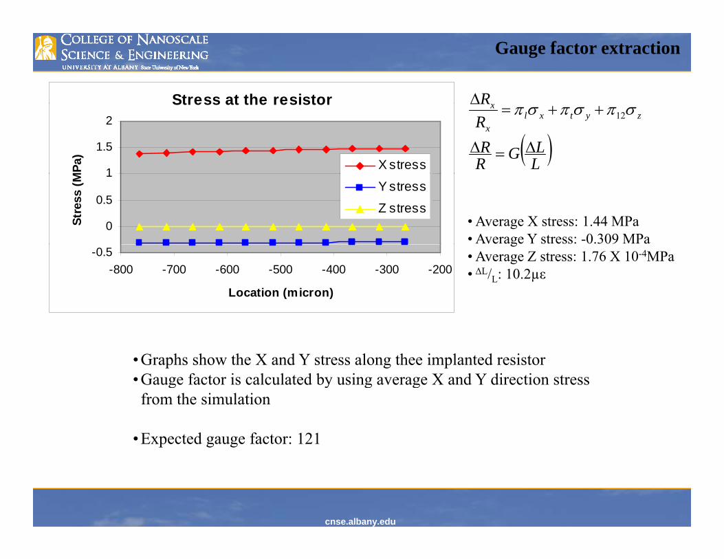
Stress at the resistor RΔ
Gauge factor extraction
Stress at the resistor
1
1.5
2
MPa
)
X stress( )L
LGRR
RR
zytxlx
x
Δ=Δ
++=Δ σπσπσπ 12
0
0.5
1
Stre
ss (M Y stress
Z stress• Average X stress: 1.44 MPa• Average Y stress: -0.309 MPa
-0.5-800 -700 -600 -500 -400 -300 -200
Location (micron)
g• Average Z stress: 1.76 X 10⁻⁴MPa• ΔL/L: 10.2µε
• Graphs show the X and Y stress along thee implanted resistor• Gauge factor is calculated by using average X and Y direction stress g y g gfrom the simulation
• Expected gauge factor: 121
cnse.albany.edu
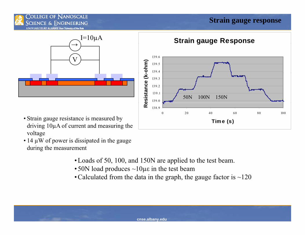
Strain gauge Response
Strain gauge response
I=10µA g g p
139.4
139.5
139.6
-ohm
)
↑
V
139.0
139.1
139.2
139.3
esis
tanc
e (k
-
50N 100N 150N
138.90 20 40 60 80 100
Tim e (s)
Re
• Strain gauge resistance is measured by driving 10µA of current and measuring the voltage
• Loads of 50, 100, and 150N are applied to the test beam.
voltage• 14 µW of power is dissipated in the gauge
during the measurement
Loads of 50, 100, and 150N are applied to the test beam. • 50N load produces ~10µε in the test beam• Calculated from the data in the graph, the gauge factor is ~120
cnse.albany.edu
St i R
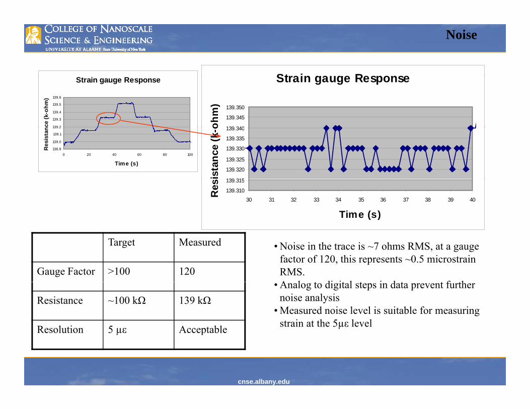
Noise
Strain gauge Response
139 340
139.345
139.350
ohm
)
Strain gauge Response
139 2
139.3
139.4
139.5
139.6
ce (k
-ohm
)
139 315
139.320
139.325
139.330
139.335
139.340
ista
nce
(k-o
138.9
139.0
139.1
139.2
0 20 40 60 80 100
Time (s)
Res
ista
n
139.310
139.315
30 31 32 33 34 35 36 37 38 39 40
Time (s)R
es
• Noise in the trace is ~7 ohms RMS, at a gauge factor of 120, this represents ~0.5 microstrain RMS.A l t di it l t i d t t f th
Target Measured
Gauge Factor >100 120• Analog to digital steps in data prevent further
noise analysis• Measured noise level is suitable for measuring
strain at the 5µε level
Resistance ~100 kΩ 139 kΩ
Resolution 5 µε Acceptable
cnse.albany.edu
µ p

SummarySummary• Large gauge factor is required for sensing strain at low powers• Piezoresistive silicon is a natural choice for its large gauge factor and ability to be batch fabricated
• Single die, multi-axis strain gauges have been designed and fabricated• Test data shows that the gauge is suitable for measuring 5 microstrain while dissipating only 14 μW of power
AcknowledgementWe would like to acknowledge Dr Hassaram Bakhru for his help with ionWe would like to acknowledge Dr. Hassaram Bakhru for his help with ion implantation as well as Lawrence Clow and Barry Treloar for their help and useful discussion.
This work was supported in part by the United States Navy, NAVAIR Contract N68335-05-C-0216
cnse.albany.edu
Thank you for your attention
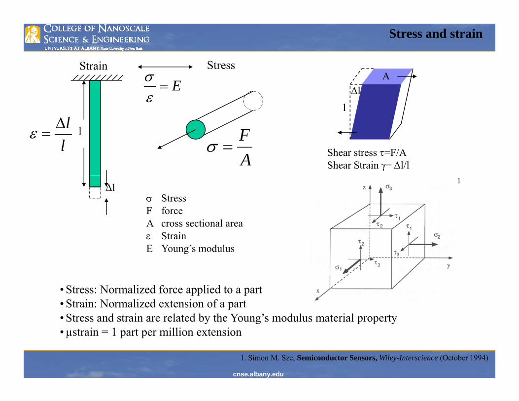
Stress and strain
Strain StressA
lΔ
E=εσ
Δll
A
lllΔ
=ε
AF
=σ Shear stress τ=F/AShear Strain γ= Δl/l
Δlσ StressF forceA cross sectional area
1
A cross sectional areaε StrainE Young’s modulus
• Stress: Normalized force applied to a part• Strain: Normalized extension of a part• Stress and strain are related by the Young’s modulus material property
cnse.albany.edu
• µstrain = 1 part per million extension
1. Simon M. Sze, Semiconductor Sensors, Wiley-Interscience (October 1994)