Embed Size (px)
Citation preview
Nano Energy 82 (2021) 105653
Available online 5 December 20202211-2855/© 2020 Elsevier Ltd. All rights reserved.
Piezotronic and piezo-phototronic effects of atomically-thin ZnO nanosheets
Chunhua An a,c,1, Hui Qi a,1, Longfei Wang b,c, Xing Fu a, Aochen Wang d,*, Zhong Lin Wang b,c,**, Jing Liu a,*
a State Key Laboratory of Precision Measuring Technology and Instrument, School of Precision Instruments and Opto-electronics Engineering, Tianjin University, 92 Weijin Rd., Tianjin 300072, PR China b Beijing Institute of Nanoenergy and Nanosystems, Chinese Academy of Sciences, Beijing 100083, PR China c School of Material Science and Engineering, Georgia Institute of Technology, Atlanta, GA 30332, United States d School of Information Engineering, Hebei GEO University, Shijiazhuang 050031, PR China
A R T I C L E I N F O
Keywords: ZnO Nanosheet Piezoelectricity Polarization Piezotronic effect Piezo-Phototronic effect
A B S T R A C T
Piezotronic and piezo-phototronic effects have attracted much attention as promising approaches for active electronic/optoelectronic devices. However, the piezotronic and piezo-phototronic devices in previous reports are mainly based on nanowires or two-dimensional transition-metal dichalcogenides that have size of several micrometers along the polarization direction. As the fast development of nanoelectronics and nano- optoelectronics, exploring the piezotronic effect and piezo-phototronic effect at nanometer scale for ultrathin nanodevices and nanosystems is valuable. Here, we investigated the piezotronic and piezo-phototronic effects of atomically thin ZnO nanosheet, and revealed the dominant mechanism. Experiments were performed on the atomically thin ZnO field effect transistor, which showed enhanced electronic transport characteristic under pressure. Theoretical analysis revealed that the change of electronic transport behavior was caused by pressure induced modulation on the effective thickness of the transport channel and the Schottky barrier between ZnO and contact electrodes. Meanwhile, the atomically-thin ZnO film exhibited enhanced response to ultraviolet light under pressure with a high photoresponsivity of 300 AW− 1 (Vds = 2 V). This value was improved 230% than the response of the same device under strain-free condition, and more than 103 times higher than the performance of commercial ultraviolet photodetectors, indicating the effectiveness of piezo-phototronic effect in nanoscale. This study shows great promises of the ultrathin devices based on piezotronic and piezo-phototronic effects, which paves the way for atomically-thin semiconductors with out-of-plane piezoelectricity for applications in novel electronics/optoelectronics.
1. Introduction
Piezotronics and piezo-phototronics are emerging fields, with great potential applications in the fields involving electronics-human/ ambience interactions, such as self-powered wearable electronics, human-machine interfacing, biomedical engineering, and robotics [1–5]. Piezotronics couples piezoelectricity and semiconducting elec-tronics of a material through stress/strain [6–14]. For instance, strain/stress induces piezoelectric polarization charges which are distributed at the surface of semiconducting material, resulting in the
formation of piezoelectric potential. The magnitude and polarity of the piezoelectric potential within a piezoelectric semiconductor depend on the polar direction of the crystal and the magnitude and direction of the mechanical actuation. The induced piezoelectric charges/potential can effectively tune the Schottky barrier formed at the metal-semiconductor (M–S) interface by affecting the redistribution of free carriers at the contact [15]. On the other hand, piezo-phototronics couples photon with piezoelectricity and semiconducting properties in third-generation semiconductors [16–19]. Specifically, the strain/stress-induced piezo-electric polarization charges may effectively tune one or more of the
* Corresponding authors. ** Corresponding author at: Beijing Institute of Nanoenergy and Nanosystems, Chinese Academy of Sciences, Beijing 100083, PR China.
E-mail addresses: [email protected] (A. Wang), [email protected] (Z.L. Wang), [email protected] (J. Liu). 1 These authors contributed equally to this work.
Contents lists available at ScienceDirect
Nano Energy
journal homepage: http://www.elsevier.com/locate/nanoen
https://doi.org/10.1016/j.nanoen.2020.105653 Received 20 October 2020; Received in revised form 24 November 2020; Accepted 30 November 2020
Nano Energy 82 (2021) 105653
2
processes during photon-semiconductor interaction, including photon-excited carrier generation, separation, transport, and recombi-nation at M–S contact and p-n junction. Besides, piezo-phototronics may also enable tunable optoelectronics by using piezoelectric polarization charges as the gate bias to tune the interface Schottky barrier or elec-tronic energy states. So far, piezotronics and piezo-phototronics have been widely demonstrated in third-generation semiconductors, such as ZnO and GaN, which have made great progress in energy harvesting (enhanced solar technology, catalysis), active electro-nics/optoelectronics (self-powered nanodevice, memory device, photo-detector) and intelligent sensing (adaptive tactile sensing, LED, human-machine interface) [1–6]. However, the feature size of these devices is in micrometer scale along the polarization direction. Fast development of nanoelectronics and nano-photoelectronic devices re-quires further shrinking device feature size down to nanoscale [20–26]. Therefore, it is highly desired to figure out the effectiveness of piezo-tronic and piezo-phototronic effects in nanometer scale.
Previously, we have demonstrated the piezotronic effect in atomi-cally thin ZnO nanosheet and proposed two mechanisms for the piezo-tronic effect, including pressure induced modulation on the metal-ZnO contact barrier and the width of the ZnO transport channel [15]. Here, we further investigated the piezotronic effect of the atomically thin ZnO nanosheet to figure out its dominant mechanism. Meanwhile, we demonstrated and studied the piezo-phototronic effect in the ZnO nanosheet for the first time. Two-terminal devices based on the ZnO ultrathin film were fabricated to realize effective modulation of elec-tronic transport via piezotronic and piezo-phototronic effects. Accu-rately controlled pressure was loaded at different locations of the same
device, which revealed that the dominant mechanism for the piezotronic effect attributed to the modulation of metal-ZnO contact barrier. Theoretical simulations of the thickness-dependent piezotronics further verified this finding. Moreover, we investigated the photoresponse of the atomically thin ZnO nanodevice to ultraviolet (UV) light. By applying strain/stress on the device to excite piezo-phototronic effect, the device achieved a high photoresponsivity of 300 AW− 1 (Vds = 2 V), which is enhanced 230% in comparison to the value obtained by the same device at strain-free condition. It is also more than 103 times higher in magnitude than that of the performance of the commercial ultraviolet photodetector. This study shows the promise of ultrathin (in polariza-tion direction) piezotronic and piezo-phototronic devices with high performance and paves the way for atomically-thin semiconductors with out-of-plane piezoelectricity in applications of novel electronics/optoelectronics.
2. Synthesis and characterization of atomically thin ZnO nanosheets
The ZnO nanosheets were synthesized by the water-air method re-ported previously [27,28]. In this method, monolayer oleylsulfate an-ions was used as the soft templet to assist the growth of ZnO nanosheets, which resulted in a layer of ZnO nanosheet synthesized at the water-air interface. The typical shape of the synthesized ZnO nanosheets was triangle with length of each side around ~10–40 µm (Fig. 1b and Fig. S1). The synthesized ZnO nanosheet was stable in the atmospheric ambience environment. Fig. 1c shows the high-resolution (HR) trans-mission electron microscope (TEM) image of a ZnO nanosheet with a
Fig. 1. Material characterization. a, Atomic model of ZnO nanosheet with wurtzite structure and its piezoelectricity. b, Scanning electron microscope (SEM) image of a ZnO nanosheet. Scale bar is 3 µm. c, HR TEM image of the ZnO nanosheet. Scale bar is 1 nm. d, AFM image of the ZnO nanosheet and its corresponding height profile. e, Absorption spectrum of ZnO nanosheet.
C. An et al.
Nano Energy 82 (2021) 105653
3
D-spacing of ~0.281 nm, which well matches the wurtzite ZnO (0001) facet (Fig. 1a). These results demonstrated the single-crystalline nature and wurtzite structure of ZnO nanosheet. The synthesized mechanism and the characterization of single-crystalline hexagonal lattice of ZnO were detailed in previous studies [27,28].
Owing to its hexagonal structure, the ZnO ultrathin nanosheet is
expected to show piezoelectric polarization along c-axis when subjected to strain or stress (Fig. 1a). The piezoelectric property of the ZnO nanosheet was demonstrated by piezoresponse force microscopy (PFM), which characterized the effective piezoelectric coefficient (deff) of the ZnO nanosheet to be 23.7 pm V− 1 [27]. Moreover, it has been reported that the d33 value is approximated twice as large as the measured deff
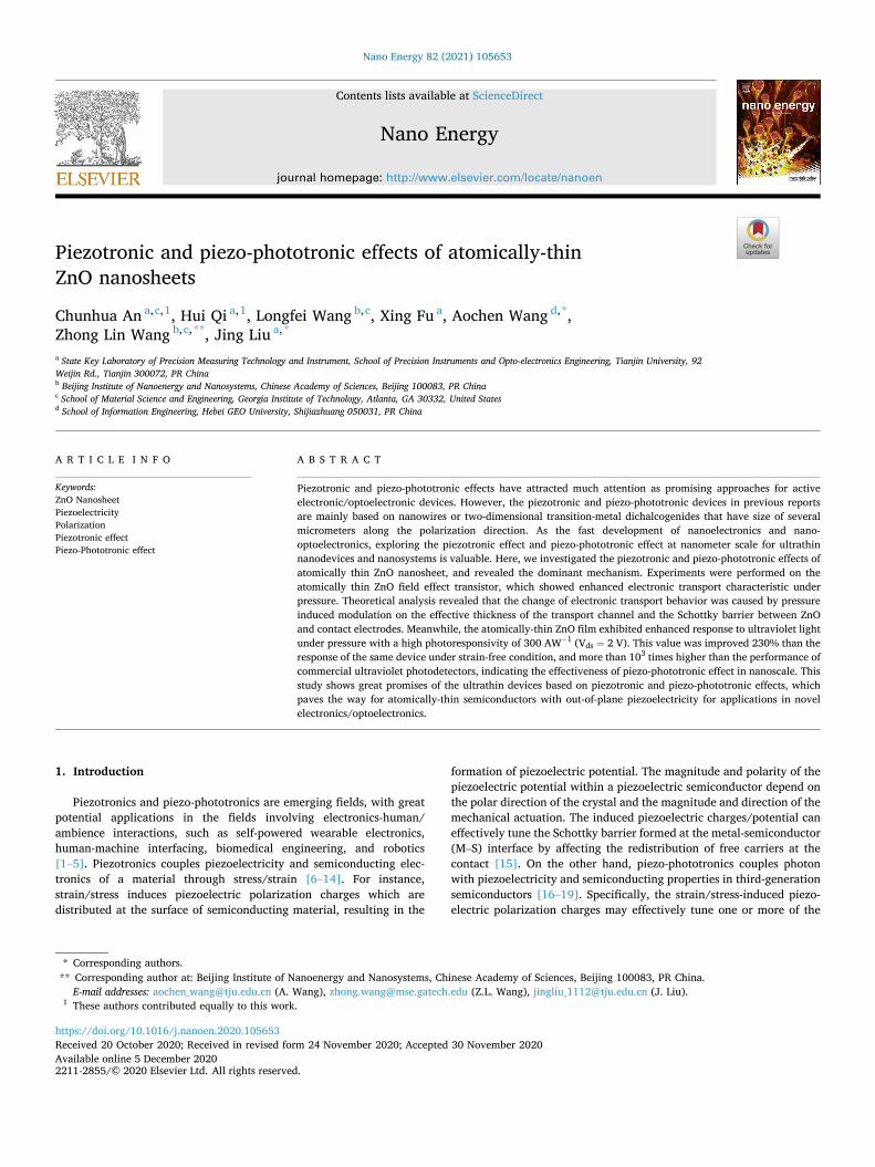
Fig. 2. Piezotronic effect at nanometer scale. a, Schematic illustration of ZnO nanosheet based piezotronic device covered by PMMA layer under force (left); electronic transport curves of the device under different pressure (middle); the mechanism of ZnO nanosheet based piezotronic device (right). b, c, Schematic illustration of the device under force on the M-S contact (left); electronic transport curves of the device under different pressure (middle); band diagram explaining the mechanism (right).φs andφd indicate the height of the Schottky barrier of source and drain electrodes, respectively. ∆E represents the change of the Schottky barrier. The energy band diagrams of the device under and without force are shown by the solid and dashed lines respectively. d, Schematic illustration of the device under force on the channel (left); electronic transport curves of the device under different pressure (middle); mechanism of piezoelectric polarization charges on the channel (right).
C. An et al.
Nano Energy 82 (2021) 105653
4
[29–31], since in the case of weak nano-indentation, the stiff tip-surface junction and high dielectric constant of the sample lead to a significant potential drop between the tip and surface. Based on this relationship, the piezoelectric coefficient d33 of the ZnO ultrathin film is much higher than the value of bulk ZnO crystal, which is presumably due to the low carrier number.
The atomic force microscope (AFM) image of the ZnO nanosheet is shown in Fig. 1d. Its thickness was measured to be 2.5 nm, which in fact comprised the thickness of the monolayer ZnO and a layer of oleylsulfate anionic. As mentioned above, oleylsulfate anionic was used as the soft template in the ZnO growth process, and thus, it was deposited on the synthesized ZnO nanosheet. Previous report indicated that the oleyl-sulfate anionic layer was around 2 nm [28]. Consequently, the synthe-sized ZnO nanosheet was around 0.5 nm thick, which matched the thickness of an atomic layer. In addition, the oleylsulfate anionic layer p-doped the ZnO nanosheet [27,28], which greatly affected the elec-trical and optical properties of the ZnO nanosheet [27,28]. The optical property of the ZnO nanosheet was characterized by the absorption and transmission spectrums, as shown in Fig. 1e and Fig. S2, respectively. In Fig. 1e, the black curve represents the absorption spectrum of bare quartz, which is transparent for light with wavelength longer than 300 nm. In contrast, the ZnO nanosheets on quartz exhibits improved absorption than bare quartz at 400 nm as plotted in the red curve, which indicates stronger light-ZnO film interaction than quartz at these wavebands. Due to the atomic thickness and influence of the oleylsulfate anionic layer, the absorption spectrum of ZnO nanosheet did not show an obvious absorption peak. The bandgap of the ZnO ultrathin film was calculated to be ~2.75 eV based on the curve of absorption coefficient (α) vs. incident photon energy (hν) as shown in Fig. S3, which was the intercept of the linear section of the curve on the x-axis. The estimated bandgap is consistent with the transparency/adsorption spectrum of ZnO thin film in terms of that photons with energy larger than 2.75 eV (wavelength shorter than 450 nm) have stronger interaction with ZnO thin film than the photons with lower energy. These indicate ZnO thin film a potential candidate for atomically-thin optoelectronic devices. In addition, due to the p-type doping induced by oleylsulfate anionic layer, strong out-of-plane piezoelectricity and stability in the atmospheric ambiance, ZnO thin film also shows great promise for atomically-thin piezotronic and piezo-phototronic devices.
3. Effectiveness of piezotronic effect at nanometer scale
We fabricated an atomically-thin ZnO based nanodevice by trans-ferring the ZnO nanofilm on SiO2/Si substrate and depositing two Au electrodes. The SEM image of one ZnO nanodevice was shown in Fig. S4. The whole nanodevice was then encapsulated by a layer of polymethyl methacrylate (PMMA) (see Fig. 2a, left). When compressive force was applied on the PMMA layer as illustrated by the red arrow in Fig. 2a, the force induced strain was homogenously applied to all parts of the device, including the Au-ZnO contacts and the ZnO channel. Thus, the piezo-electric polarization charges were induced over the surfaces of the entire ZnO nanosheet, resulting in the redistribution of carriers inside the ZnO nanosheet as shown in the right panel of Fig. 2a. The middle panel of Fig. 2a shows that the conductance of the device increases with the applied force, which may attribute to two modulating effects. One of the effects comes from the modulation of the Au-ZnO Schottky barrier by the piezoelectric polarization charges, called Au–ZnO interface modulating effect. The other effect modifies the effective thickness of the transport channel by the piezoelectric polarization charges distributed at both surfaces of the ZnO channel (Fig. 2a, right). It worth noting that the piezotronic effect in atomically-thin ZnO is different from that of nanowires or 2D TMDs reported in previous literatures [20–25]. The mechanism of piezotronic effect on nanowires and TMDs are mainly from the interface modulating at the M–S contact and/or p-n junction, while the modulating on the transport channel is neglected due to the macro-scale thickness of the transport channel along polarization
direction. In contrast, the atomic-thickness of the ZnO nanosheet de-termines that its electrical property can be modulated by both effects at contacts and transport channel.
Control experiment was then conducted to isolate the modulation effects at contacts and transport channel to characterize the contribution of both effects to the electrical property of the ZnO nanosheet. We removed the encapsulated PMMA layer from the ZnO device and applied force on Au–ZnO contact and ZnO channel separately. When the compressive force is applied on electrodes as shown in the left panels of Fig. 2b and c, the conductance of the nanodevice increases with the force (see middle panel of Fig. 2b and c), which are mainly attributed to the interface modulating effect. The right panels of Fig. 2b and c plot the energy band diagrams of the device without (dashed line) and under (solid line) pressure applied at electrode. According to the polarization direction of the ZnO film, the stress-induced negative piezoelectric po-larization charges distribute on the top surface of the ZnO film (positive charges are at the bottom surface), which is in contact with metal electrodes. Since the ZnO film is p-doped, these negative charges consume local majority carriers of holes and lower the hole density. As a result, the bands of ZnO at the M-S interface are flattened, resulting in the decrease of Au–ZnO Schottky barriers and the enhancement of the electrical conductance. In contrast, when the force is applied on the ZnO channel as shown in the left panel of Fig. 2d, the current of the device obviously decreases as the force increases (see the middle panel of Fig. 2d). In this situation, the stress-induced negative and positive piezoelectric polarization charges distribute on the top and bottom surfaces of the ZnO nanosheet, respectively. As the negative piezoelec-tric polarization charges consume local holes, free carrier holes move toward the top surface due to diffusion effect and repulsion from posi-tive piezoelectric polarization charges at the bottom surface. Conse-quently, holes accumulate near the top surface of the ZnO film, while a depletion layer is formed near the bottom of ZnO. This reduces the thickness of the carrier transport channel, and thus, increases the resistance of the channel (see right panel of Fig. 2d). These results indicate that the working mechanism of strain-gated atomically-thin ZnO device comes from the piezotronic effects including Au–ZnO con-tact barrier and channel thickness modulating, which demonstrates that the piezotronic effect is effective at the nanometer scale.
4. Theoretical simulations of piezotronic effect at nanometer scale
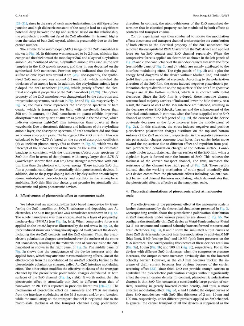
The effectiveness of the piezotronic effect at the nanometer scale is further demonstrated by the theoretical simulations presented in Fig. 3. Corresponding results about the piezoelectric polarization distribution in ZnO nanosheets under various pressures are shown in Fig. S5. We configure the atomically-thin ZnO device as Metal-Semiconductor-Metal (M–S–M) structure and assumed Schottky barriers formed at source and drain electrodes. Fig. 3a, b and c show the simulated output curves of three ZnO devices under contact interface modulation by applying 0 MP (blue line), 5 MP (orange line) and 10 MP (pink line) pressures on the M–S interface. The corresponding thicknesses of these devices are 2 nm (Fig. 3a), 10 nm (Fig. 3b) and 100 nm (Fig. 3c), respectively. For all the devices with different ZnO thicknesses, when the compressive pressure increases, the output current increases obviously due to the lowered Schottky barrier. However, as the ZnO film becomes thicker, the in-crease of drain current becomes less obvious because of the carrier screening effect [32], since thick ZnO can provide enough carriers to neutralize the piezoelectric polarization charges without significantly affect the overall carrier density. In contrast, piezoelectric polarization charges in thin ZnO film consumes a considerably large portion of car-riers, resulting in greatly lowered carrier density, and thus, a more effective modulating effect. Fig. 3d, e and f exhibit the output curves of three ZnO nanodevices with ZnO film thickness of 2 nm, 10 nm and 100 nm, respectively, under different pressure applied on ZnO channel. In general, the carrier transport of all the devices is suppressed as the
C. An et al.
Nano Energy 82 (2021) 105653
5
pressure applied on ZnO channel increases. Nevertheless, the magnitude of the current decrease is inversely proportional to the thickness of the ZnO film: when the ZnO film becomes thinner, the current decreases more significantly. This trend is consistent with the trend of contact interface modulation effect on ZnO nanodevice. However, as compared to the M–S contact modulating effect, the magnitude of channel modulating effect is much less, which suggests that the Schottky
junctions play a dominant role in the electrical transport characteristics in this case. The modulating effect on channel thickness may become more significant in nanodevice with Ohmic contact. These results further demonstrate the effectiveness of the piezotronic effect at nano-meter scale.
Fig. 3. Theoretically calculated piezotronic effect on ZnO device. I-V characteristics of ZnO based piezotronic devices with Schottky contacts. (a-c) Transfer characteristics of the ZnO devices with thickness of 2 nm (a), 10 nm (b) and 100 nm (c) under 10 MPa (pink), 5 MPa (orange) and 0 MPa (blue) applied at M-S contacts. (d-f) Transfer characteristics of the ZnO devices with thickness of 2 nm (d), 10 nm (e) and 100 nm (f) under 10 MPa (pink), 5 MPa (orange) and 0 MPa (blue) applied at transport channel.
C. An et al.
Nano Energy 82 (2021) 105653
6
5. Performance of atomically-thin ZnO photodetector
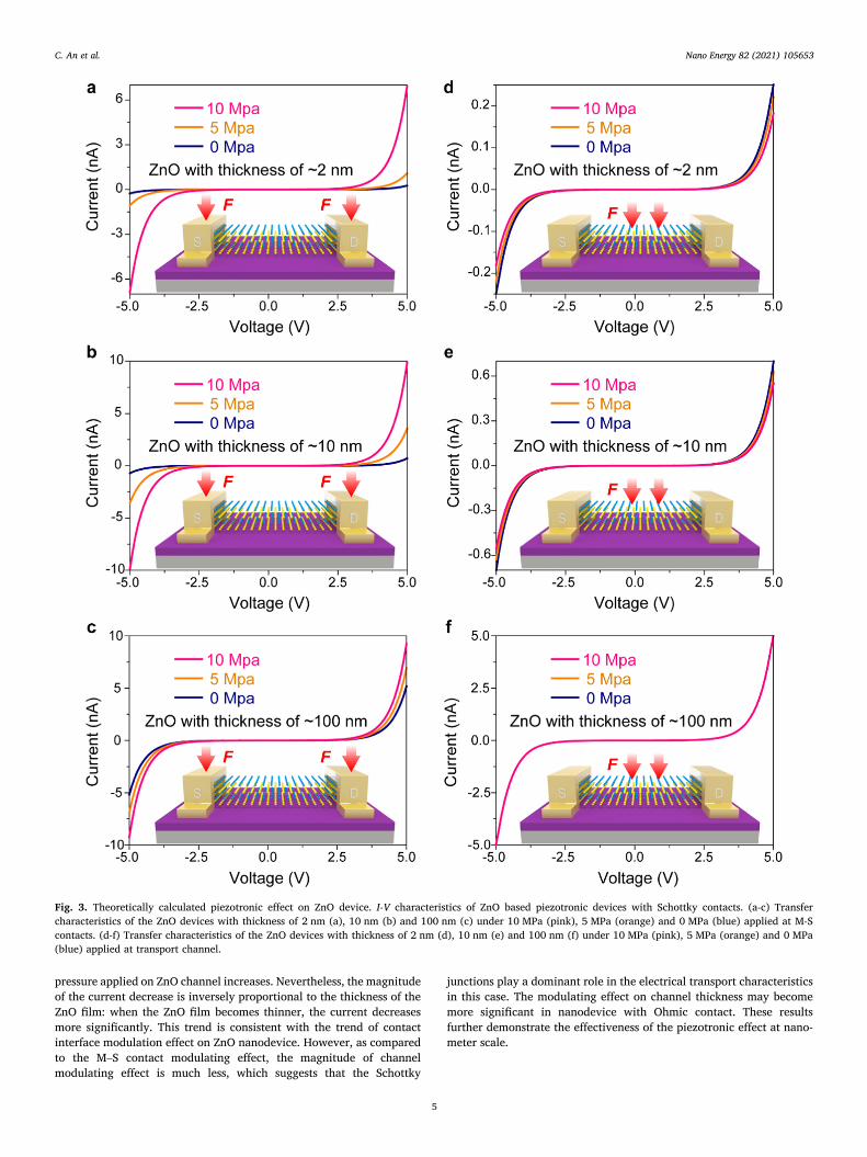
The photoresponse of the atomically-thin ZnO device is shown in Fig. 4. The I-V characteristics of the device under dark and UV illumi-nation with different intensities are shown in Fig. 4a. It can be seen that the output current of the device is significantly improved with the in-crease of illumination intensity. Fig. 4b shows the time-resolved pho-toresponse of the device under a fixed bias of 2.0 V and an illumination power intensity of 2 mW/cm2. The drain current changes instantly and significantly as the laser is switched on and off. The estimated rise time and fall time are τr ≈ 0.5 s and τd ≈ 0.9 s, respectively, with on-off current ratio of ~20. Fig. 4c plots the photocurrent (defined as Ids −
Idark) of the ZnO photodetector as a function of incident light intensity, which as expected increases as light intensity. Fig. 4d shows the pho-toresponsivity (R) of the atomically thin ZnO photodetector under different illumination power, which is calculated by the formula: R =
(Ilight - Idark)/Pillumination, where Ilight and Idark are output currents under light and light-free condition without compressive force, and Pillumination is the illumination power on the device. The photoresponsivity de-creases slightly as light intensity increases, which may be because of the saturation of ZnO thin film by the incident light. The maximum
photoresponsivity reaches 300 A/W (Vds =2 V) at an illumination power intensity of 0.01 mW/cm2, which exhibits a high sensitivity.
6. Effectiveness of piezo-phototronic effect at nanometer scale
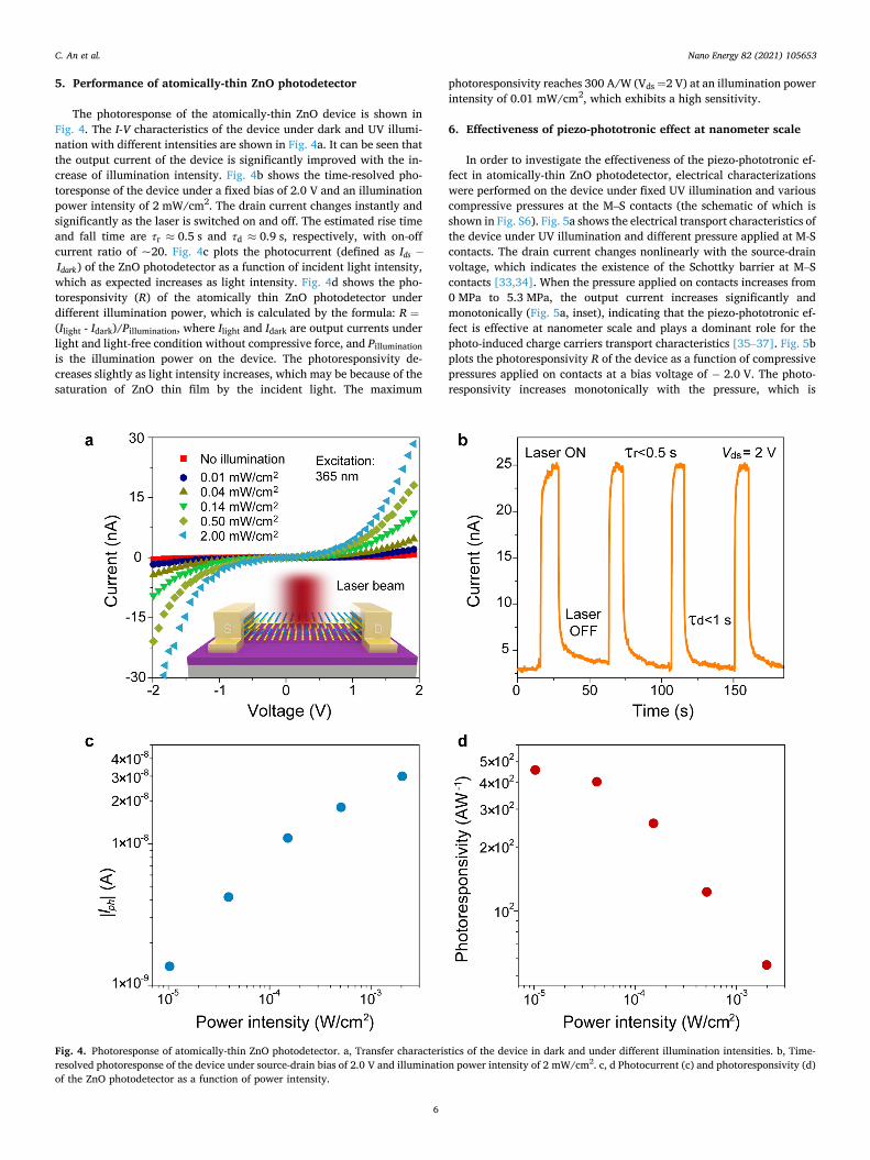
In order to investigate the effectiveness of the piezo-phototronic ef-fect in atomically-thin ZnO photodetector, electrical characterizations were performed on the device under fixed UV illumination and various compressive pressures at the M–S contacts (the schematic of which is shown in Fig. S6). Fig. 5a shows the electrical transport characteristics of the device under UV illumination and different pressure applied at M-S contacts. The drain current changes nonlinearly with the source-drain voltage, which indicates the existence of the Schottky barrier at M–S contacts [33,34]. When the pressure applied on contacts increases from 0 MPa to 5.3 MPa, the output current increases significantly and monotonically (Fig. 5a, inset), indicating that the piezo-phototronic ef-fect is effective at nanometer scale and plays a dominant role for the photo-induced charge carriers transport characteristics [35–37]. Fig. 5b plots the photoresponsivity R of the device as a function of compressive pressures applied on contacts at a bias voltage of − 2.0 V. The photo-responsivity increases monotonically with the pressure, which is
Fig. 4. Photoresponse of atomically-thin ZnO photodetector. a, Transfer characteristics of the device in dark and under different illumination intensities. b, Time- resolved photoresponse of the device under source-drain bias of 2.0 V and illumination power intensity of 2 mW/cm2. c, d Photocurrent (c) and photoresponsivity (d) of the ZnO photodetector as a function of power intensity.
C. An et al.
Nano Energy 82 (2021) 105653
7
gradually saturated as pressure exceeds 3 MPa. The photoresponsivity achieved 300 AW− 1 (Vds = 2 V) under UV illumination with power in-tensity of 10 μWcm− 2 and compressive pressure of 5.3 MPa on Au–ZnO contact. This value is enhanced 230% as compare to the value under pressure-free condition, and is more than 3 orders of magnitude larger than the value of commercial ultraviolet photodetectors (0.1–0.2 AW− 1) [38,39].
The working mechanism of the piezo-phototronic effect in enhancing atomically-thin photodetector can be explained by the band diagram as shown in Fig. 5c. Under the pressure-free condition, the large Schottky barriers of M–S junctions severely limits the photocurrent across the M–S Schottky junction, when weak illumination and low bias voltage are applied. This can be considered as OFF state, resulting in an advantage of small dark current. Upon compressive stress on M–S con-tacts of the photodetector, the stress-induced negative piezoelectric polarization charges can decrease the Schottky barriers of both contacts, which can effectively separate the electron-hole pairs and result in a high photo-response. This can be considered as an ON state. These re-sults demonstrate that the piezo-phototronic effect can greatly improve the performance of atomically-thin ZnO photodetector, which shows promise for high-performance piezo-phototronic devices at nanometer
scale. The thickness of the ZnO nanosheet may also influence the piezo-
phototronic effect. As the ZnO film becomes thicker, the number of free carriers (holes) in the ZnO film increases, which presents stronger screening effect to counteract the negative piezoelectric polarization charges at the metal-ZnO interface, leading to the less obvious metal- ZnO contact modulating effect. Consequently, the piezo-phototronic effect is expected to be inversely corelated with the thickness of the ZnO nanosheet. More in-depth investigations are still demanded to reveal the thickness-dependent piezo-phototronic effect.
7. Conclusion
To summarize, the piezotronic and piezo-phototronic effects have been simultaneously demonstrated in atomically-thin ZnO nanosheet. Owing to its atomic thickness and strong out-of-plane piezoelectricity, the electrical transport of ZnO nanodevice can be effectively tuned by the piezotronic effect including interface modulating effect (using inner piezo-potential at metal-semiconductor contact to tune the Schottky barrier) and channel thickness modulating effect (using inner piezo- potential of ZnO nanosheet to gate the channel thickness). Control
Fig. 5. Piezo-phototronic effect enhanced atomically-thin ZnO photodetector. a, Transfer characteristic of the ZnO device under different pressure applied at M-S contacts when the source-drain bias is 2 V and illumination intensity is 10 μW cm− 2. The inset shows the photocurrent as function of applied pressures. b, Photo-responsivity of ZnO photodetector as a function of applied pressure at M-S contact. c, Band diagrams of the atomically-thin ZnO photodetector under illumination with (right) and without (left) pressure applied at M–S contacts. ΦB represents the height of Schottky barrier.
C. An et al.
Nano Energy 82 (2021) 105653
8
experiments and theoretical calculations discovered the dominant mechanism for the piezotronic effect to be the interface barrier modu-lating. Furthermore, atomically-thin ZnO photodetector has been implemented and achieved enhanced performance under the piezo- phototronic effect modulation. It exhibits a high photoresponsivity of 300 AW− 1 (Vds = 2 V) under compressive pressure of 5.3 MPa applied on Au–ZnO contacts, which is improved 230% as compared to the value under pressure-free condition and more than 103 times larger than the value of commercial UV photodetectors. This work shows great promise of ultrathin piezotronic and piezo-phototronic devices and paves the way of atomically-thin semiconductors with out-of-plane piezoelec-tricity for electromechanical and photo-electromechanical nanodevice and nanosystem applications.
CRediT authorship contribution statement
C.H.A, J.L. conceived the project and designed the experiments. C.H. A. and H.Q. performed the experiments. L.F.W. performed the theoret-ical calculations. C.H.A., L.F.W. and A.C.W. analyzed the results. All authors contributed to discussions and writing of the manuscript.
Declaration of Competing Interest
The authors declare that they have no known competing financial interests or personal relationships that could have appeared to influence the work reported in this paper.
Acknowledgments
This project has been supported by the National Science Foundation of China (NSFC Grant No. 52075385), Seed Foundation of State Key Laboratory of Precision Measurement Technology and Instruments (Pilt No. 1710) and International Cultivation Program for Top Doctoral Dis-sertations of Tianjin University in 2019.
Appendix A. Supporting information
Supplementary data associated with this article can be found in the online version at doi:10.1016/j.nanoen.2020.105653.
References
[1] Z.L. Wang, W. Wen, C. Falconi, Piezotronics and piezo-phototronics with third- generation semiconductors, MRS Bull. 43 (2018) 922–927.
[2] Z.L. Wang, Progress in Piezotronics and piezo-phototronics, Adv. Mater. 24 (2012) 4632–4646.
[3] Z.L. Wang, W.Z. Wu, Piezotronics and piezo-phototronics: fundamentals and applications, Natl. Sci. Rev. 1 (2014) 62–90.
[4] W.Z. Wu, Z.L. Wang, Piezotronics and piezo-phototronics for adaptive electronics and optoelectronics, Nat. Rev. Mater. 1 (2016) 16031.
[5] C. Pan, J. Zhai, Z.L. Wang, Piezotronics and piezo-phototronics of third generation semiconductor nanowires, Chem. Rev. 119 (2019) 9303–9359.
[6] Z.L. Wang, Piezotronics and Piezo-Phototronics, Springer, New York, 2013. [7] Z.L. Wang, Nanopiezotronics, Adv. Mater. 19 (2007) 889–892. [8] Z.L. Wang, The new field of nanopiezotronics, Mater. Today 10 (2007) 20–28. [9] Y. Zhang, Y. Liu, Z.L. Wang, Fundamental theory of piezotronics, Adv. Mater. 23
(2011) 3004–3013. [10] Y. Zhang, Y. Leng, M. Willatzen, B. Huang, Theory of piezotronics and piezo-
phototronics, MRS Bull. 43 (2018) 928–935. [11] H. Yan, Z. Feng, S. Shang, X. Wang, Z. Hu, J. Wang, Z. Zhu, H. Wang, Z. Chen,
H. Hua, W. Lu, J. Wang, P. Qin, H. Guo, X. Zhou, Z. Leng, Z. Liu, C. Jiang, M. Coey, Z. Liu, A piezoelectric, strain-controlled antiferromagnetic memory insensitive to magnetic fields, Nat. Nanotechnol. 14 (2019) 131–136.
[12] S.S. Won, M. Kawahara, S. Glinsek, J. Lee, Y. Kim, C.K. Jeong, A.I. Kingon, S. H. Kim, Flexible vibrational energy harvesting devices using strain-engineered perovskite piezoelectric thin films, Nano Energy 55 (2019) 182–192.
[13] X. Zhou, K. Parida, O. Halevi, Y. Liu, J. Xiong, S. Magdassi, P.S. Lee, All 3D-printed stretchable piezoelectric nanogenerator with non-protruding kirigami structure, Nano Energy 72 (2020), 104676.
[14] S. Ahn, Y. Cho, S. Park, J. Kim, J. Sun, D. Ahn, M. Lee, D. Kim, T. Kim, H. Shin, J. J. Park, Wearable multimode sensors with amplified piezoelectricity due to the multi local strain using 3D textile structure for detecting human body signals, Nano Energy 74 (2020), 104932.
[15] L. Wang, S. Liu, Z. Zhang, X. Feng, L. Zhu, H. Guo, W. Ding, L. Chen, Y. Qin, Z. L. Wang, 2D piezotronics in atomically thin zinc oxide sheets: interfacing gating and channel width gating, Nano Energy 60 (2019) 724–733.
[16] Q. Yang, X. Guo, W. Wang, Y. Zhang, S. Xu, D.H. Lien, Z.L. Wang, Enhancing sensitivity of a single ZnO micro-/nanowire photodetector by piezo-phototronic effect, ACS Nano 4 (2010) 6285–6291.
[17] Q. Yang, W. Wang, S. Xu, Z.L. Wang, Enhancing light emission of ZnO microwire- based diodes by piezo-phototronic effect, Nano Lett. 11 (2011) 4012–4017.
[18] Y. Liu, S.M. Niu, Q. Yang, B.D.B. Klein, Y.S. Zhou, Z.L. Wang, Theoretical study of piezo-phototronic nano-leds, Adv. Mater. 26 (2014) 7209–7216.
[19] Y. Liu, Q. Yang, Y. Zhang, Z.Y. Yang, Z.L. Wang, Nanowire piezo-phototronic photodetector: theory and experimental design, Adv. Mater. 24 (2012) 1410–1417.
[20] W.Z. Wu, L. Wang, Y.L. Li, F. Zhang, L. Lin, S.M. Niu, D. Chenet, X. Zhang, Y. F. Hao, T.F. Heinz, J. Hone, Z.L. Wang, Piezoelectricity of single-atomic-layer MoS2 for energy conversion and piezotronics, Nature 514 (2014) 470–474.
[21] W.Z. Wu, X.N. Wen, Z.L. Wang, Taxel-addressable matrix of vertical-nanowire piezotronic transistors for active and adaptive tactile imaging, Science 340 (2013) 952–957.
[22] S. Liu, L. Wang, X. Feng, Z. Wang, Q. Xu, S. Bai, Y. Qin, Z.L. Wang, Ultrasensitive 2D ZnO piezotronic transistor array for high resolution tactile imaging, Adv. Mater. 29 (2017), 1606346.
[23] S. Liu, L. Wang, Z. Wang, Y. Cai, X. Feng, Y. Qin, Z.L. Wang, Double-channel piezotronic transistors for highly sensitive pressure sensing, ACS Nano 12 (2018) 1732–1738.
[24] L. Wang, S. Liu, X. Feng, Q. Xu, S. Bai, L. Zhu, L. Chen, Y. Qin, Z.L. Wang, Ultrasensitive vertical piezotronic transistor based on ZnO twin nanoplatelet, ACS Nano 11 (2017) 4859–4865.
[25] W. Wu, Y. Wei, Z.L. Wang, Strain-gated piezotronic logic nanodevices, Adv. Mater. 22 (2010) 4711–4715.
[26] C. An, Z. Xu, W. Shen, R. Zhang, Z. Sun, S. Tang, Y.F. Xiao, D. Zhang, D. Sun, X. Hu, C. Hu, L. Yang, J. Liu, The opposite anisotropic piezoresistive effect of ReS2, ACS Nano 13 (2019) 3310–3319.
[27] L. Wang, S. Liu, G. Gao, Y. Pang, X. Yin, X. Feng, L. Zhu, Y. Bai, L. Chen, T. Xiao, X. Wang, Y. Qin, Z.L. Wang, Ultrathin piezotronic transistors with 2 nm channel lengths, ACS Nano 12 (2018) 4903–4908.
[28] F. Wang, J.H. Seo, G.F. Luo, M.B. Starr, Z.D. Li, D.L. Geng, X. Yin, S.Y. Wang, D. G. Fraser, D. Morgan, Z.Q. Ma, X.D. Wang, Nanometre-thick single-crystalline nanosheets grown at the water–air interface, Nat. Commun. 7 (2016) 10444.
[29] X. Wang, X. He, H. Zhu, L. Sun, W. Fu, X. Wang, L.C. Hoong, H. Wang, Q. Zeng, W. Zhao, J. Wei, Z. Jin, Z. Shen, J. Liu, T. Zhang, Z. Liu, Subatomic deformation driven by vertical piezoelectricity from CdS ultrathin films, Sci. Adv. 2 (7) (2016), https://doi.org/10.1126/sciadv.1600209 e1600209.
[30] S.V. Kalinin, D.A. Bonnell, Imaging mechanism of piezoresponse force microscopy of ferroelectric surfaces, Phys. Rev. B 65 (2002), 125408.
[31] F. Johann, A. Hoffmann, E. Soergel, Impact of electrostatic forces in contact-mode scanning force microscopy, Phys. Rev. B 81 (2010), 094109.
[32] Y. Gao, Z.L. Wang, Equilibrium potential of free charge carriers in a bent piezoelectric semiconductive nanowire, Nano Lett. 9 (3) (2009) 1103–1110.
[33] M.W. Allen, S.M. Durbin, J.B. Metson, Silver oxide Schottky contacts on n-type ZnO, Appl. Phys. Lett. 91 (2007), 053512.
[34] R. Zhang, C. An, L. Xu, S. Wu, D. Zhang, X. Hu, J. Liu, Homogenous Tunnel Diode Based on Two-Dimensional Molybdenum Disulfide with Light Induced n+ Doping, ACS Appl. Electron. Mater. 1 (2019) 523–529.
[35] L. Pan, S. Sun, Y. Chen, P. Wang, J. Wang, X. Zhang, J.J. Zou, Z.L. Wang, Advances in piezo-phototronic effect enhanced photocatalysis and photoelectrocatalysis, Adv. Energy Mater. 10 (2020), 2000214.
[36] L. Zhu, Q. Lai, W. Zhai, B. Chen, Z.L. Wang, Piezo-phototronic effect enhanced polarization-sensitive photodetectors based on cation-mixed organic-inorganic perovskite nanowires, Mater. Today 37 (2020) 56–63.
[37] L. Zhu, Z.L. Wang, Recent progress in piezo-phototronic effect enhanced solar cells, Adv. Funct. Mater. 29 (2019), 1808214.
[38] E. Monroy, F. Omnes, F. Calle, Wide-bandgap semiconductor ultraviolet photodetectors, Semicond. Sci. Technol. 18 (2003) R33–R51.
[39] J. Zou, Q. Zhang, K. Huang, N. Marzari, Ultraviolet photodetectors based on anodic TiO2 nanotube arrays, J. Phys. Chem. C. 114 (2010) 10725–10729.
Chunhua AN received his B.S. (2013) and M.S. (2016) in Mechanical engineering from Taiyuan University of Science and Technology and North University of China, respectively. Now he is a Ph.D student at Tianjin University. Currently, he is a visiting scholar (2019–2021) in Prof. Zhong Lin Wang’s group at Georgia Tech. His research mainly focuses on the development of multifunctional semiconductor devices and application of nanomaterial based on piezotronics, piezo- phototronics, flexible device and optoelectronic.
C. An et al.

Nano Energy 82 (2021) 105653
9
Hui Qi is currently pursuing her PhD degree under the super-vision of Prof. Xing Fu in the State Key Laboratory of Precision Measuring Technology and Instruments at Tianjin University. Her research focuses on the material growth of thin films, characterizations of organic-inorganic hybrid heterostructures and analytical techniques of detected interfaces.
Longfei Wang received his B.S. (2012) in Materials Science and Engineering from China University of Geosciences (Bei-jing) and Ph.D. (2017) in Nanoscience and Technology from Beijing Institute of Nanoenergy and Nanosystems, Chinese Academy of Sciences. He is now a postdoctoral fellow at Georgia Institute of Technology. His current research focuses on piezotronics, piezo-phototronics and flexo-electronics.
Xing Fu Ph.D. Professor, vice director of State Key Laboratory of Precision Measuring Technology and Instruments at Tianjin University. Receipted the State Scientific and Technological Progress Award in 2005. More than 140 research papers have been published. More than 50 Chinese invention patents have been authorized. Research interests include the techniques of growth, characterization and fabrication of thin films and film- devices.
Aochen Wang received her Ph.D. from Tianjin University in Department of Microelectronics in 2020. Currently, she is a lecturer in Hebei GEO University. Her research interests include piezoelectric materials, self-powered medical devices, flexible sensors.
Zhong Lin Wang received his Ph.D. from Arizona State Uni-versity in physics. He is the Hightower Chair in Materials Sci-ence and Engineering, Regents’ Professor at Georgia Tech. Dr. Wang has made original and innovative contributions to the synthesis, discovery, characterization and understanding of fundamental physical properties of oxide nanobelts and nano-wires, as well as applications of nanowires in energy sciences, electronics, optoelectronics and biological science. His dis-covery and breakthroughs in developing nanogenerators established the principle and technological road map for har-vesting mechanical energy from environment and biological systems for powering personal electronics. His research on self- powered nanosystems has inspired the worldwide effort in academia and industry for studying energy for micro-nano- systems, which is now a distinct disciplinary in energy research and future sensor networks. He coined and pioneered the field of piezotronics and piezo phototronics by introducing piezoelectric potential gated charge transport process in fabricating new electronic and optoelectronic devices. Details can be found at: http://www.nanoscience.gatech.edu.
Jing Liu received her B.S. and Master’s degree at Optoelec-tronics Department at Huazhong University of Science and Technology in 2006 and 2008, respectively. Then, she received Ph.D. degree at Department of Biomedical Engineering, Uni-versity of Michigan-Ann Arbor. Currently, she is an associate professor at School of Precision Instruments and Optoelec-tronics Engineering, Tianjin University, since 2013. Her research interest mainly focuses on nanoscale functional de-vices and sensors.
C. An et al.