Embed Size (px)
Citation preview
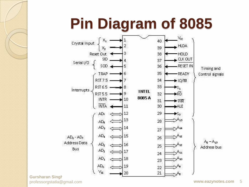
PIN DIAGRAM OF 8085
GURSHARAN SINGH TATLA
www.eazynotes.com
Gursharan Singh Tatla
[email protected] 1www.eazynotes.com
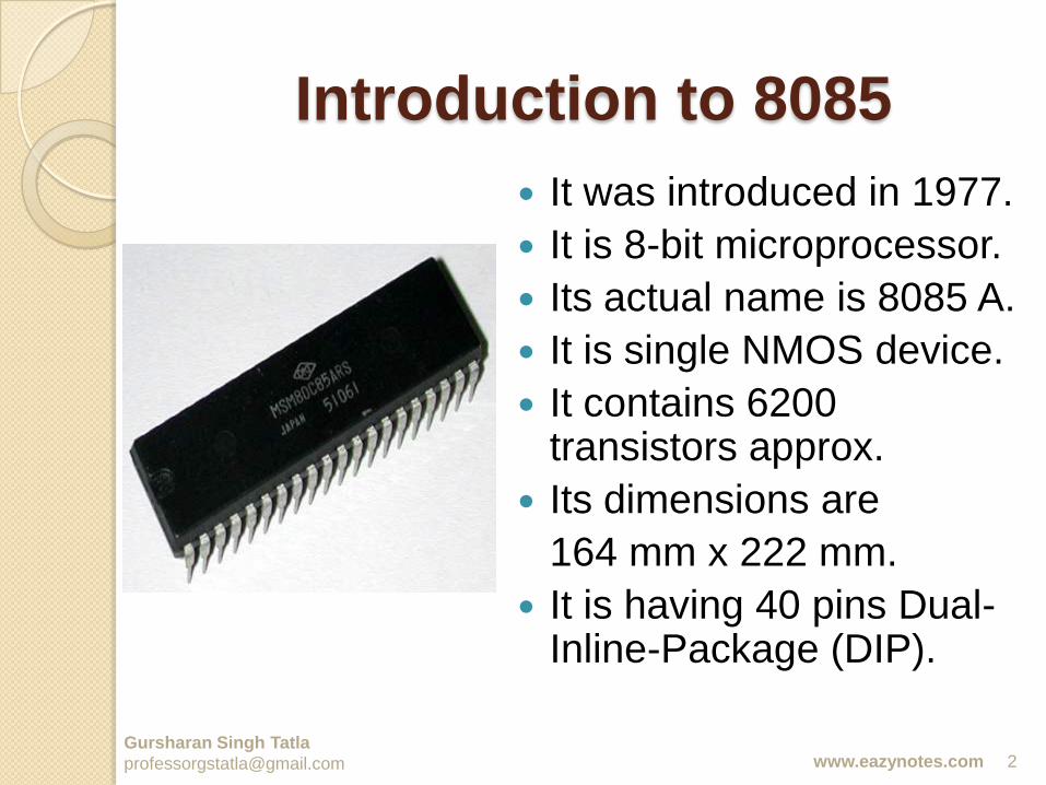
Introduction to 8085
It was introduced in 1977.
It is 8-bit microprocessor.
Its actual name is 8085 A.
It is single NMOS device.
It contains 6200 transistors approx.
Its dimensions are
164 mm x 222 mm.
It is having 40 pins Dual-Inline-Package (DIP).
Gursharan Singh Tatla
[email protected] 2www.eazynotes.com

Introduction to 8085
It has three advanced versions:◦ 8085 AH
◦ 8085 AH2
◦ 8085 AH1
These advanced versions are designed using HMOS technology.
Gursharan Singh Tatla
[email protected] 3www.eazynotes.com

Introduction to 8085
The advanced versions consume 20% less power supply.
The clock frequencies of 8085 are:◦ 8085 A 3 MHz
◦ 8085 AH 3 MHz
◦ 8085 AH2 5 MHz
◦ 8085 AH1 6 MHz
Gursharan Singh Tatla
[email protected] 4www.eazynotes.com
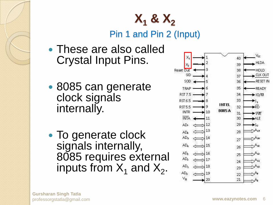
X1 & X2
Pin 1 and Pin 2 (Input)
Gursharan Singh Tatla
These are also called Crystal Input Pins.
8085 can generate clock signals internally.
To generate clock signals internally, 8085 requires external inputs from X1 and X2.
www.eazynotes.com
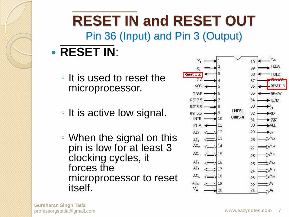
RESET IN and RESET OUTPin 36 (Input) and Pin 3 (Output)
Gursharan Singh Tatla
RESET IN:
◦ It is used to reset the microprocessor.
◦ It is active low signal.
◦ When the signal on this pin is low for at least 3 clocking cycles, it forces the microprocessor to reset itself.
www.eazynotes.com
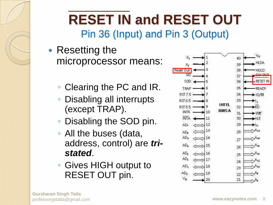
RESET IN and RESET OUTPin 36 (Input) and Pin 3 (Output)
Gursharan Singh Tatla
Resetting the microprocessor means:
◦ Clearing the PC and IR.
◦ Disabling all interrupts (except TRAP).
◦ Disabling the SOD pin.
◦ All the buses (data, address, control) are tri-stated.
◦ Gives HIGH output to RESET OUT pin.
www.eazynotes.com
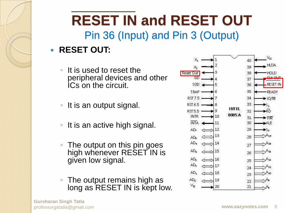
RESET IN and RESET OUTPin 36 (Input) and Pin 3 (Output)
Gursharan Singh Tatla
RESET OUT:
◦ It is used to reset the peripheral devices and other ICs on the circuit.
◦ It is an output signal.
◦ It is an active high signal.
◦ The output on this pin goes high whenever RESET IN is given low signal.
◦ The output remains high as long as RESET IN is kept low.
www.eazynotes.com
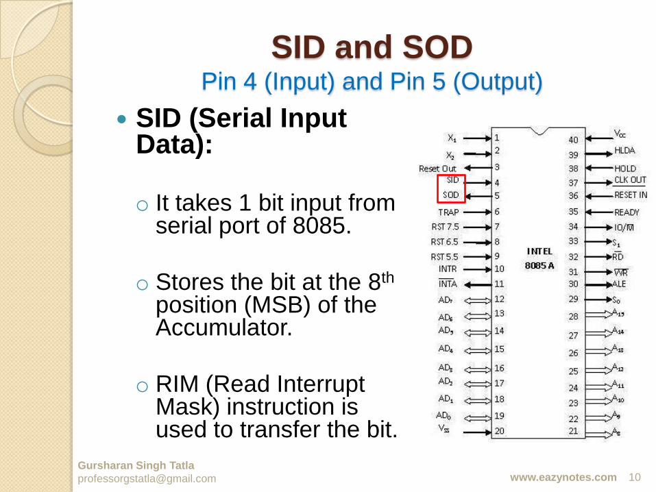
SID and SODPin 4 (Input) and Pin 5 (Output)
Gursharan Singh Tatla
SID (Serial Input Data):
o It takes 1 bit input from serial port of 8085.
o Stores the bit at the 8th
position (MSB) of the Accumulator.
o RIM (Read Interrupt Mask) instruction is used to transfer the bit.
www.eazynotes.com
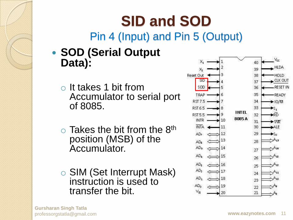
SID and SODPin 4 (Input) and Pin 5 (Output)
Gursharan Singh Tatla
SOD (Serial Output Data):
o It takes 1 bit from Accumulator to serial port of 8085.
o Takes the bit from the 8th
position (MSB) of the Accumulator.
o SIM (Set Interrupt Mask) instruction is used to transfer the bit.
www.eazynotes.com
Interrupt Pins
Gursharan Singh Tatla
Interrupt:
• It means interrupting the normal execution of the microprocessor.
• When microprocessor receives interrupt signal, it discontinues whatever it was executing.
• It starts executing new program indicated by the interrupt signal.
• Interrupt signals are generated by external peripheral devices.
• After execution of the new program, microprocessor goes back to the previous program.
www.eazynotes.com
Sequence of Steps Whenever There
is an Interrupt
Gursharan Singh Tatla
Microprocessor completes execution of current instruction of the program.
PC contents are stored in stack.
PC is loaded with address of the new program.
After executing the new program, the microprocessor returns back to the previous program.
It goes to the previous program by reading the top value of stack.
www.eazynotes.com
Five Hardware Interrupts in 8085
Gursharan Singh Tatla
TRAP
RST 7.5
RST 6.5
RST 5.5
INTR
www.eazynotes.com
Classification of Interrupts
Gursharan Singh Tatla
Maskable and Non-Maskable
Vectored and Non-Vectored
Edge Triggered and Level Triggered
Priority Based Interrupts
www.eazynotes.com
Maskable Interrupts
Gursharan Singh Tatla
Maskable interrupts are those
interrupts which can be enabled or
disabled.
Enabling and Disabling is done by
software instructions.
www.eazynotes.com
Maskable Interrupts
Gursharan Singh Tatla
List of Maskable Interrupts:
• RST 7.5
• RST 6.5
• RST 5.5
• INTR
www.eazynotes.com
Non-Maskable Interrupts
Gursharan Singh Tatla
The interrupts which are always in
enabled mode are called non-
maskable interrupts.
These interrupts can never be
disabled by any software instruction.
TRAP is a non-maskable interrupt.
www.eazynotes.com
Vectored Interrupts
Gursharan Singh Tatla
The interrupts which have fixed
memory location for transfer of
control from normal execution.
Each vectored interrupt points to the
particular location in memory.
www.eazynotes.com
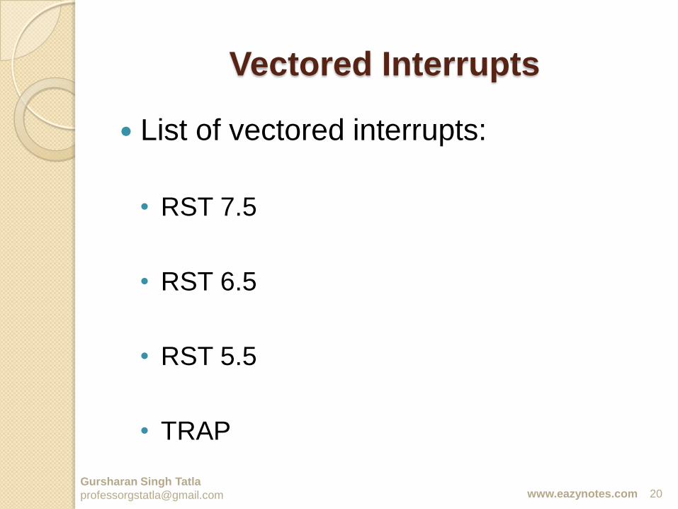
Vectored Interrupts
Gursharan Singh Tatla
List of vectored interrupts:
• RST 7.5
• RST 6.5
• RST 5.5
• TRAP
www.eazynotes.com
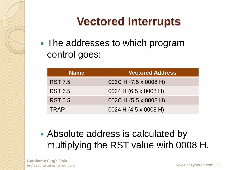
Vectored Interrupts
Gursharan Singh Tatla
The addresses to which program
control goes:
Absolute address is calculated by
multiplying the RST value with 0008 H.
Name Vectored Address
RST 7.5 003C H (7.5 x 0008 H)
RST 6.5 0034 H (6.5 x 0008 H)
RST 5.5 002C H (5.5 x 0008 H)
TRAP 0024 H (4.5 x 0008 H)
www.eazynotes.com
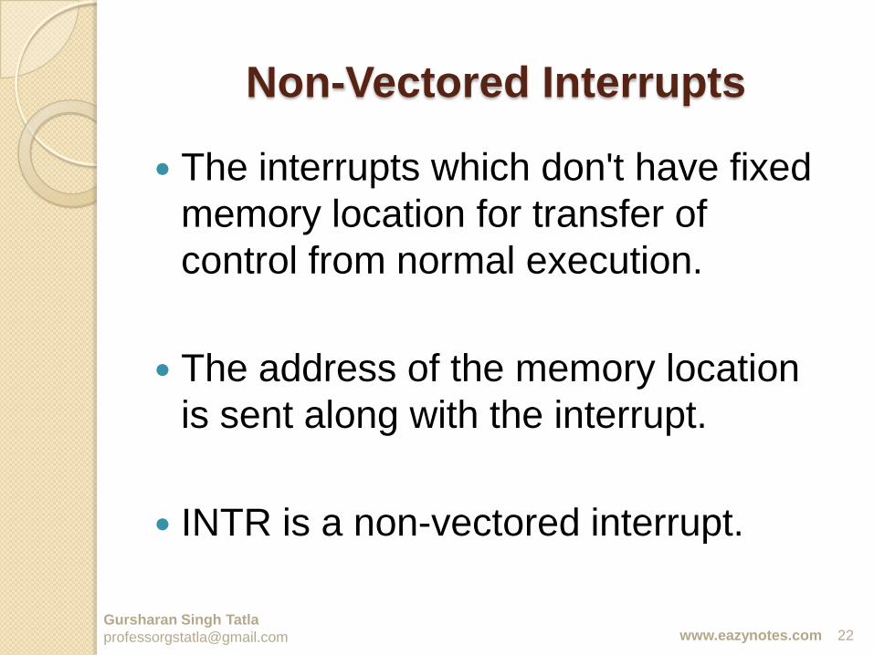
Non-Vectored Interrupts
Gursharan Singh Tatla
The interrupts which don't have fixed
memory location for transfer of
control from normal execution.
The address of the memory location
is sent along with the interrupt.
INTR is a non-vectored interrupt.
www.eazynotes.com
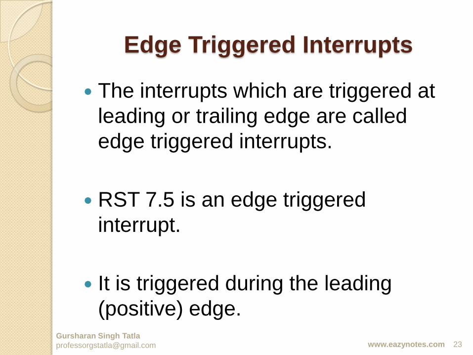
Edge Triggered Interrupts
Gursharan Singh Tatla
The interrupts which are triggered at
leading or trailing edge are called
edge triggered interrupts.
RST 7.5 is an edge triggered
interrupt.
It is triggered during the leading
(positive) edge.
www.eazynotes.com
Level Triggered Interrupts
Gursharan Singh Tatla
The interrupts which are triggered at high or low level are called level triggered interrupts.
RST 6.5
RST 5.5
INTR
TRAP is edge and level triggered interrupt.
www.eazynotes.com
Priority Based Interrupts
Gursharan Singh Tatla
Whenever there exists a
simultaneous request at two or more
pins then the pin with higher priority
is selected by the microprocessor.
Priority is considered only when there
are simultaneous requests.
www.eazynotes.com
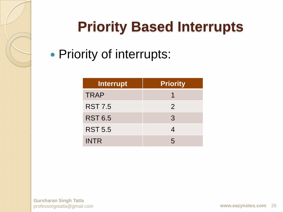
Priority Based Interrupts
Gursharan Singh Tatla
Priority of interrupts:
Interrupt Priority
TRAP 1
RST 7.5 2
RST 6.5 3
RST 5.5 4
INTR 5
www.eazynotes.com
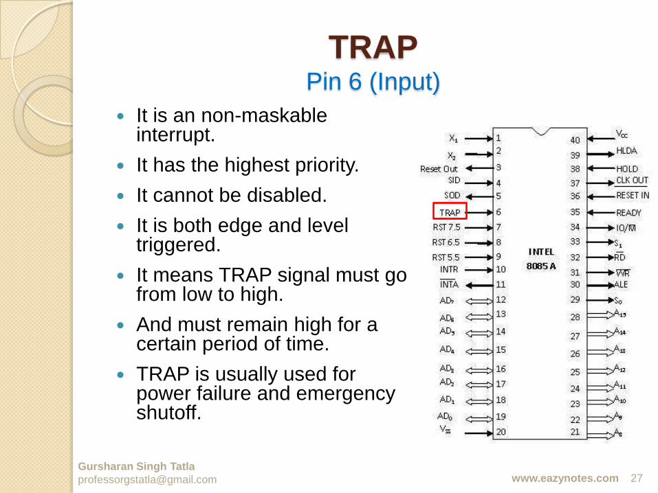
TRAPPin 6 (Input)
Gursharan Singh Tatla
It is an non-maskable interrupt.
It has the highest priority.
It cannot be disabled.
It is both edge and level triggered.
It means TRAP signal must go from low to high.
And must remain high for a certain period of time.
TRAP is usually used for power failure and emergency shutoff.
www.eazynotes.com
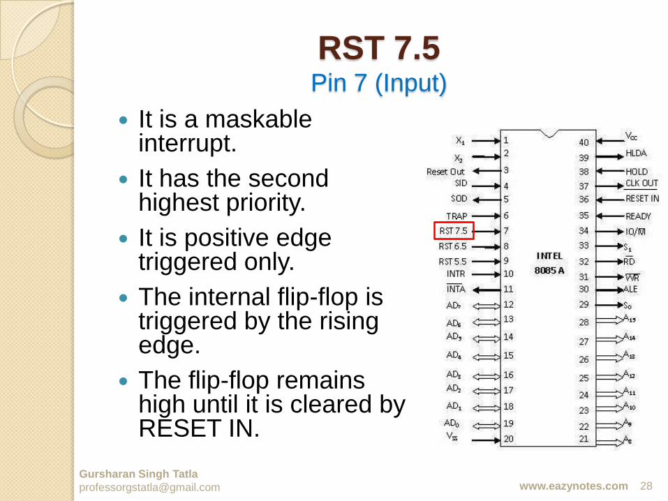
RST 7.5Pin 7 (Input)
Gursharan Singh Tatla
It is a maskable interrupt.
It has the second highest priority.
It is positive edge triggered only.
The internal flip-flop is triggered by the rising edge.
The flip-flop remains high until it is cleared by RESET IN.
www.eazynotes.com
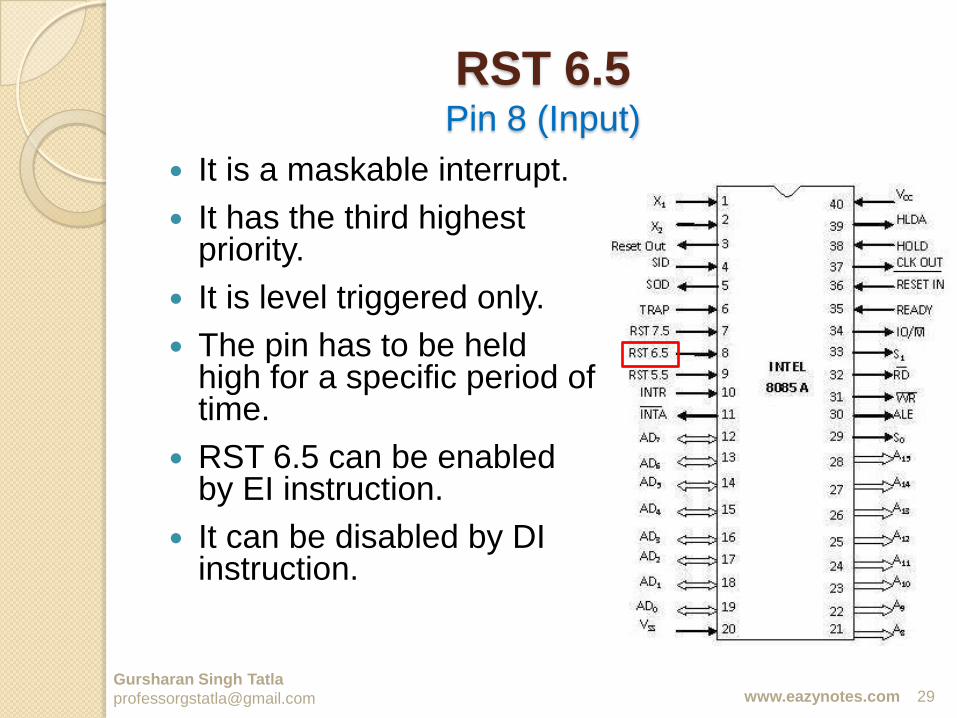
RST 6.5Pin 8 (Input)
Gursharan Singh Tatla
It is a maskable interrupt.
It has the third highest priority.
It is level triggered only.
The pin has to be held high for a specific period of time.
RST 6.5 can be enabled by EI instruction.
It can be disabled by DI instruction.
www.eazynotes.com
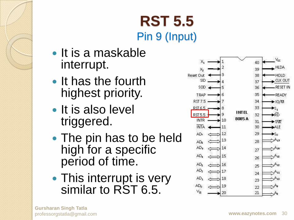
RST 5.5Pin 9 (Input)
Gursharan Singh Tatla
It is a maskable interrupt.
It has the fourth highest priority.
It is also level triggered.
The pin has to be held high for a specific period of time.
This interrupt is very similar to RST 6.5.
www.eazynotes.com
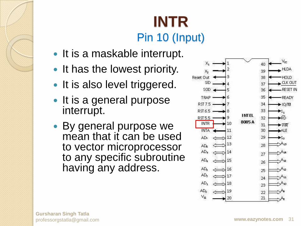
INTRPin 10 (Input)
Gursharan Singh Tatla
It is a maskable interrupt.
It has the lowest priority.
It is also level triggered.
It is a general purpose interrupt.
By general purpose we mean that it can be used to vector microprocessor to any specific subroutine having any address.
www.eazynotes.com
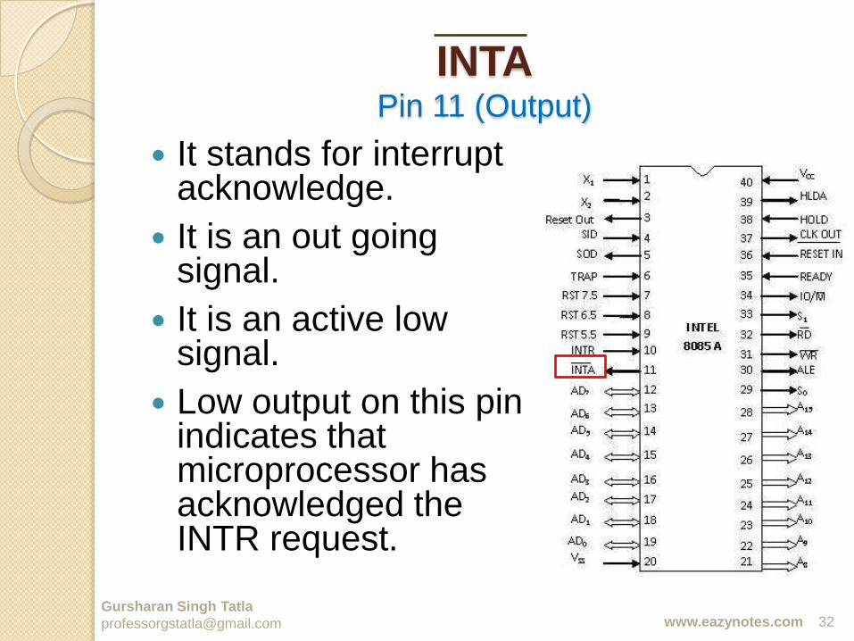
INTAPin 11 (Output)
Gursharan Singh Tatla
It stands for interrupt acknowledge.
It is an out going signal.
It is an active low signal.
Low output on this pin indicates that microprocessor has acknowledged the INTR request.
www.eazynotes.com
Address and Data Pins
Gursharan Singh Tatla
Address Bus:
• The address bus is used to send
address to memory.
• It selects one of the many locations in
memory.
• Its size is 16-bit.
www.eazynotes.com
Address and Data Pins
Gursharan Singh Tatla
Data Bus:
• It is used to transfer data between
microprocessor and memory.
• Data bus is of 8-bit.
www.eazynotes.com
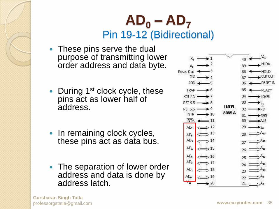
AD0 – AD7Pin 19-12 (Bidirectional)
Gursharan Singh Tatla
These pins serve the dual purpose of transmitting lower order address and data byte.
During 1st clock cycle, these pins act as lower half of address.
In remaining clock cycles, these pins act as data bus.
The separation of lower order address and data is done by address latch.
www.eazynotes.com
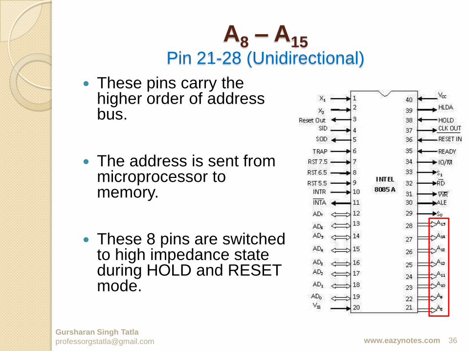
A8 – A15Pin 21-28 (Unidirectional)
Gursharan Singh Tatla
These pins carry the higher order of address bus.
The address is sent from microprocessor to memory.
These 8 pins are switched to high impedance state during HOLD and RESET mode.
www.eazynotes.com
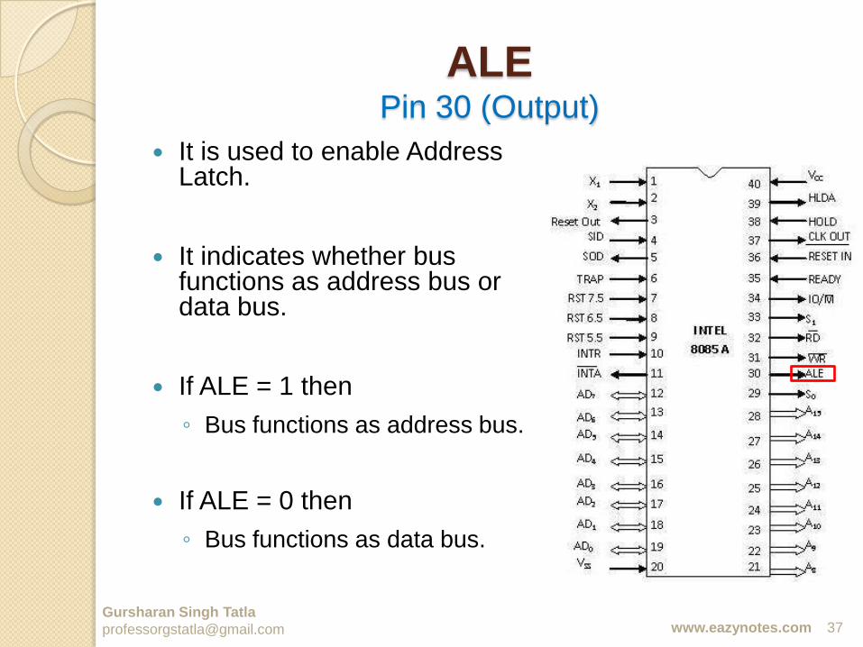
ALEPin 30 (Output)
Gursharan Singh Tatla
It is used to enable Address Latch.
It indicates whether bus functions as address bus or data bus.
If ALE = 1 then
◦ Bus functions as address bus.
If ALE = 0 then
◦ Bus functions as data bus.
www.eazynotes.com
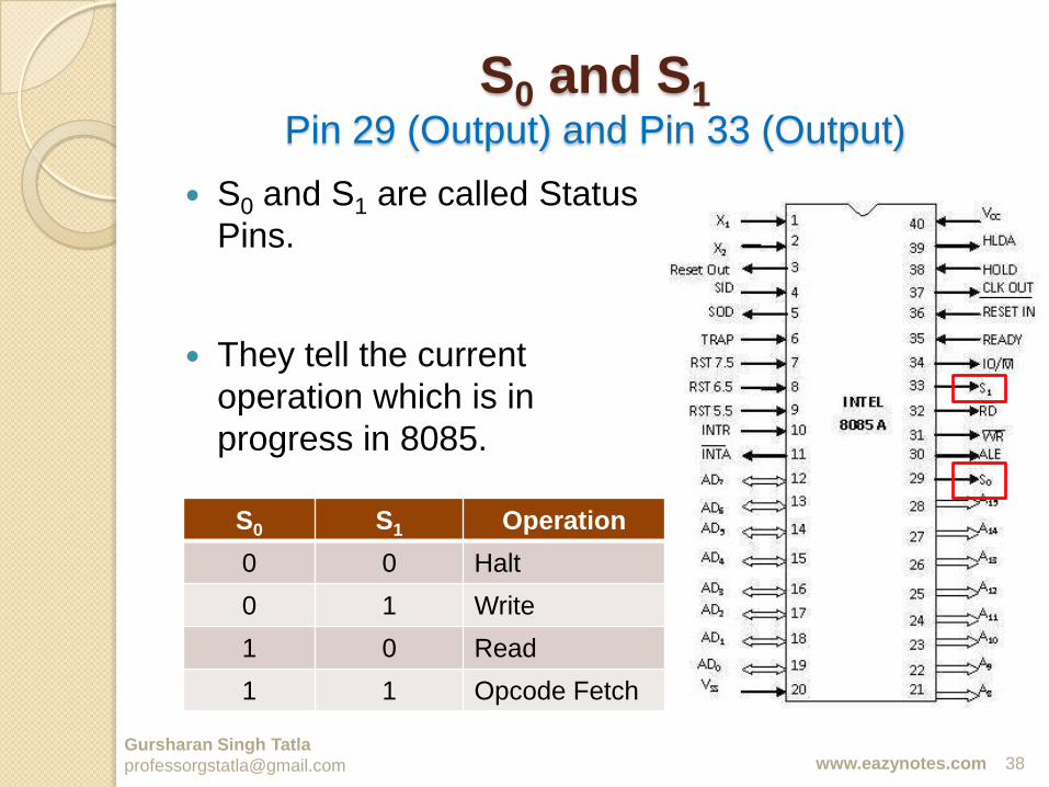
S0 and S1Pin 29 (Output) and Pin 33 (Output)
Gursharan Singh Tatla
S0 and S1 are called Status
Pins.
They tell the current
operation which is in
progress in 8085.
S0 S1 Operation
0 0 Halt
0 1 Write
1 0 Read
1 1 Opcode Fetch
www.eazynotes.com
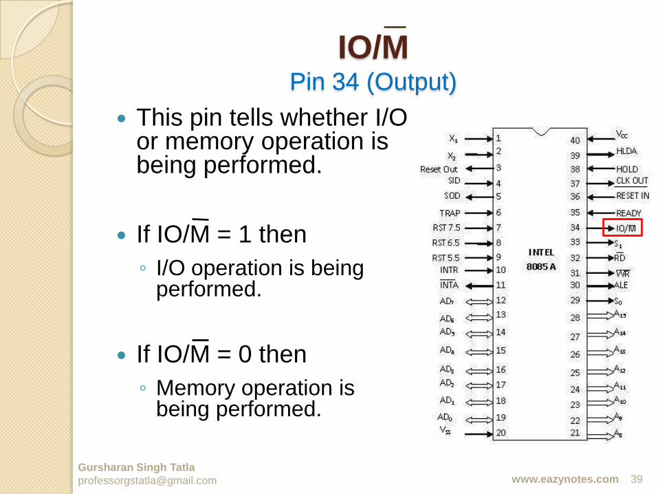
IO/MPin 34 (Output)
Gursharan Singh Tatla
This pin tells whether I/O or memory operation is being performed.
If IO/M = 1 then
◦ I/O operation is being performed.
If IO/M = 0 then
◦ Memory operation is being performed.
www.eazynotes.com
IO/MPin 34 (Output)
Gursharan Singh Tatla
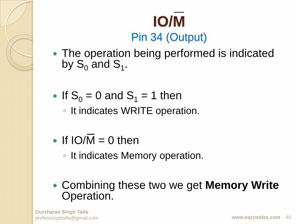
The operation being performed is indicated by S0 and S1.
If S0 = 0 and S1 = 1 then
◦ It indicates WRITE operation.
If IO/M = 0 then
◦ It indicates Memory operation.
Combining these two we get Memory WriteOperation.
www.eazynotes.com
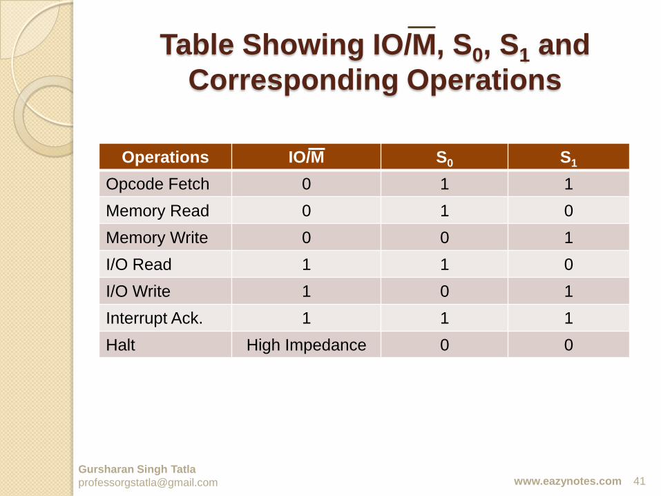
Table Showing IO/M, S0, S1 and
Corresponding Operations
Gursharan Singh Tatla
Operations IO/M S0 S1
Opcode Fetch 0 1 1
Memory Read 0 1 0
Memory Write 0 0 1
I/O Read 1 1 0
I/O Write 1 0 1
Interrupt Ack. 1 1 1
Halt High Impedance 0 0
www.eazynotes.com
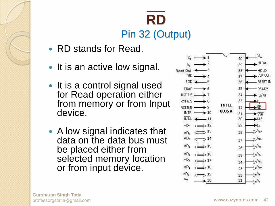
RDPin 32 (Output)
Gursharan Singh Tatla
RD stands for Read.
It is an active low signal.
It is a control signal used for Read operation either from memory or from Input device.
A low signal indicates that data on the data bus must be placed either from selected memory location or from input device.
www.eazynotes.com
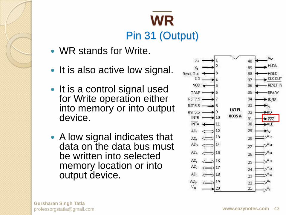
WRPin 31 (Output)
Gursharan Singh Tatla
WR stands for Write.
It is also active low signal.
It is a control signal used for Write operation either into memory or into output device.
A low signal indicates that data on the data bus must be written into selected memory location or into output device.
www.eazynotes.com
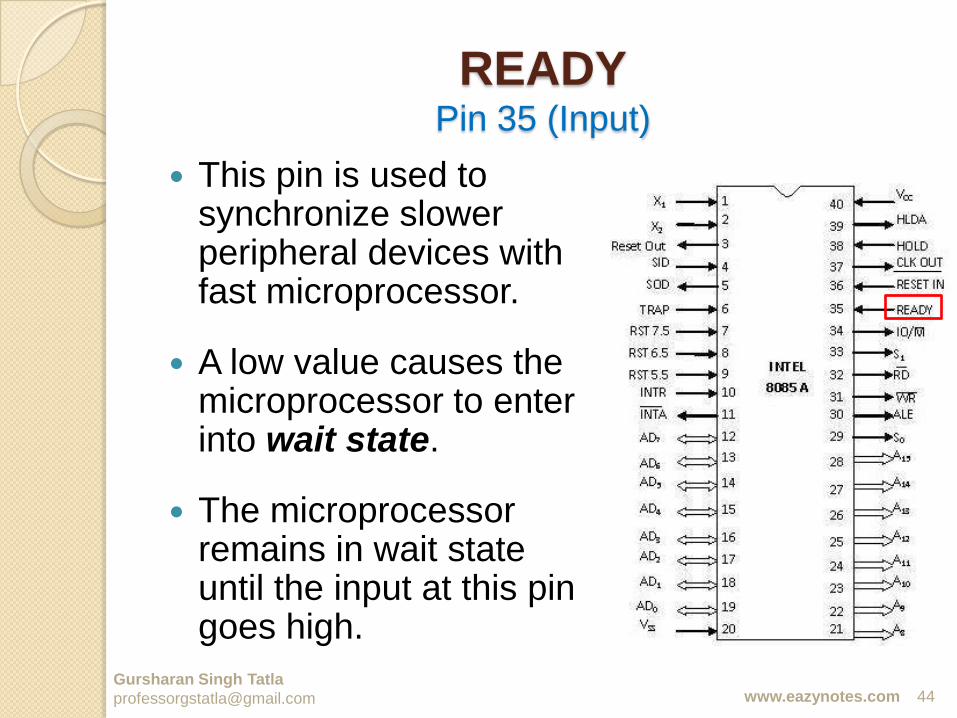
READYPin 35 (Input)
Gursharan Singh Tatla
This pin is used to synchronize slower peripheral devices with fast microprocessor.
A low value causes the microprocessor to enter into wait state.
The microprocessor remains in wait state until the input at this pin goes high.
www.eazynotes.com
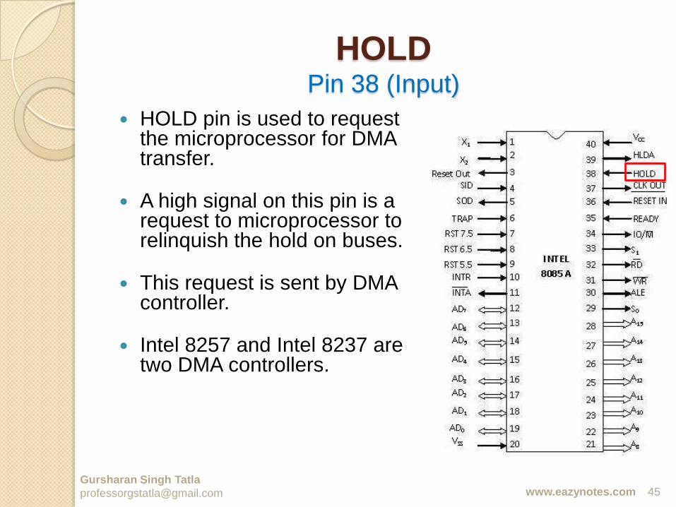
HOLDPin 38 (Input)
Gursharan Singh Tatla
HOLD pin is used to request the microprocessor for DMA transfer.
A high signal on this pin is a request to microprocessor to relinquish the hold on buses.
This request is sent by DMA controller.
Intel 8257 and Intel 8237 are two DMA controllers.
www.eazynotes.com
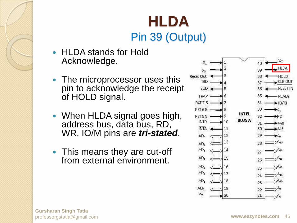
HLDAPin 39 (Output)
Gursharan Singh Tatla
HLDA stands for Hold Acknowledge.
The microprocessor uses this pin to acknowledge the receipt of HOLD signal.
When HLDA signal goes high, address bus, data bus, RD, WR, IO/M pins are tri-stated.
This means they are cut-off from external environment.
www.eazynotes.com
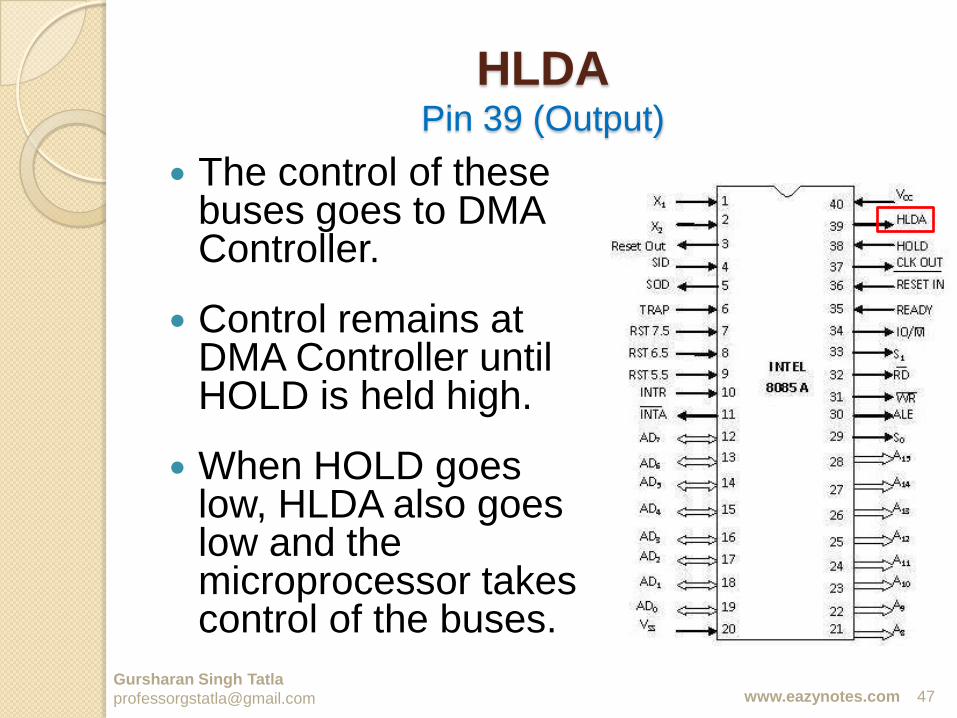
HLDAPin 39 (Output)
Gursharan Singh Tatla
The control of these buses goes to DMA Controller.
Control remains at DMA Controller until HOLD is held high.
When HOLD goes low, HLDA also goes low and the microprocessor takes control of the buses.
www.eazynotes.com
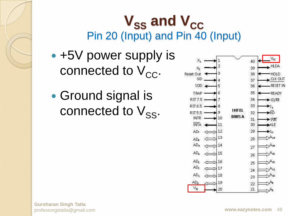
VSS and VCCPin 20 (Input) and Pin 40 (Input)
Gursharan Singh Tatla
+5V power supply is
connected to VCC.
Ground signal is
connected to VSS.
www.eazynotes.com


![STUDY & EVALUATION SCHEME Diploma in …...Size, The 8085 Microprocessor Unit, Architecture & Description. UNIT-II [8] Pin Diagram of 8085, Addressing Modes of 8085, Data Transfer](https://img.pdfslide.net/doc/110x75/5f7989d5625c5716621e9faf/study-evaluation-scheme-diploma-in-size-the-8085-microprocessor-unit.jpg)