Embed Size (px)
DESCRIPTION
Plans and Progress on the FPGA+ADC Card Pack. Chris Tully Princeton University Upgrade Workshop, Fermilab October 28, 2009. General Concept. 180 mm. 8 Optical Fibers. 75 mm. 72 HB/HE RBX, 4 RM/RBX, 8 Fibers/RM 2304 Digital Links in HB/HE. More Depth Segmentation in HCAL. Upgrade - PowerPoint PPT Presentation
Citation preview

Plans and Progress on the FPGA+ADC Card
Pack
Chris Tully
Princeton University
Upgrade Workshop, Fermilab
October 28, 2009

Upgrade Workshop, October, FNAL
General Concept
2
8 Optical Fibers
180 mm
75 mm
• 72 HB/HE RBX, 4 RM/RBX, 8 Fibers/RM– 2304 Digital Links in HB/HE

More Depth Segmentation in HCAL
Upgrade Workshop, October, FNAL 3
3
Current18-Channel RMs
Upgrade64-Channel HB RMs48-Channel HE RMs
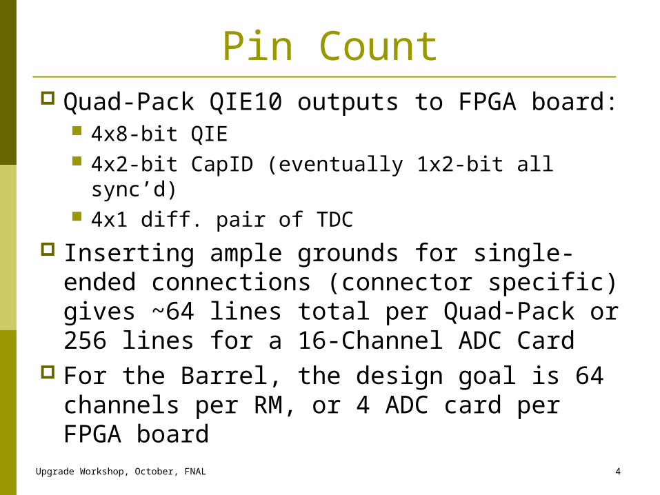
Pin Count Quad-Pack QIE10 outputs to FPGA board:
4x8-bit QIE 4x2-bit CapID (eventually 1x2-bit all sync’d) 4x1 diff. pair of TDC
Inserting ample grounds for single-ended connections (connector specific) gives ~64 lines total per Quad-Pack or 256 lines for a 16-Channel ADC Card
For the Barrel, the design goal is 64 channels per RM, or 4 ADC card per FPGA board
Upgrade Workshop, October, FNAL 4

Mechanical Mock-up of FPGA card
UMN design of FPGA card with 3x100 pin Samtec connectors
End connector is for backplane interface board (I2C, LV power and clocks)
Upgrade Workshop, October, FNAL 5

Samtec Connectors
Upgrade Workshop, October, FNAL 6

Mechanical Mock-up of ADC card
UMN design of ADC card End connectors make board removal
somewhat difficult – could be a problem Also gets I2C, LV power and clocks from
backplane interface board
Upgrade Workshop, October, FNAL 7

Mechanical Mock-up of Interface Board
UMN design of Interface Board Mates to RBX backplane and CCM system Provides I2C, LV power and clocks Problem with Connector Alignment in
Current Design
Upgrade Workshop, October, FNAL 8
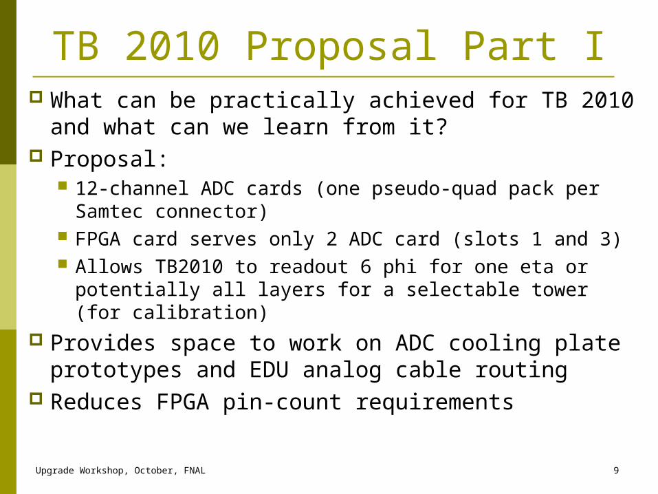
TB 2010 Proposal Part I What can be practically achieved for TB 2010
and what can we learn from it? Proposal:
12-channel ADC cards (one pseudo-quad pack per Samtec connector)
FPGA card serves only 2 ADC card (slots 1 and 3) Allows TB2010 to readout 6 phi for one eta or
potentially all layers for a selectable tower (for calibration)
Provides space to work on ADC cooling plate prototypes and EDU analog cable routing
Reduces FPGA pin-count requirementsUpgrade Workshop, October, FNAL 9
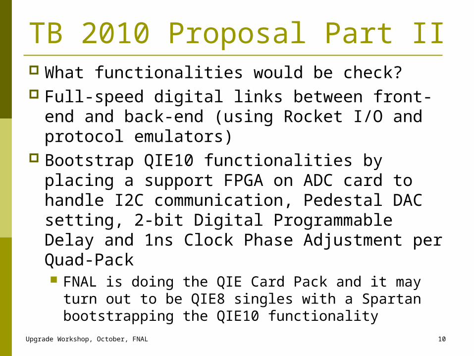
TB 2010 Proposal Part II What functionalities would be check? Full-speed digital links between front-end
and back-end (using Rocket I/O and protocol emulators)
Bootstrap QIE10 functionalities by placing a support FPGA on ADC card to handle I2C communication, Pedestal DAC setting, 2-bit Digital Programmable Delay and 1ns Clock Phase Adjustment per Quad-Pack FNAL is doing the QIE Card Pack and it may
turn out to be QIE8 singles with a Spartan bootstrapping the QIE10 functionality
Upgrade Workshop, October, FNAL 10
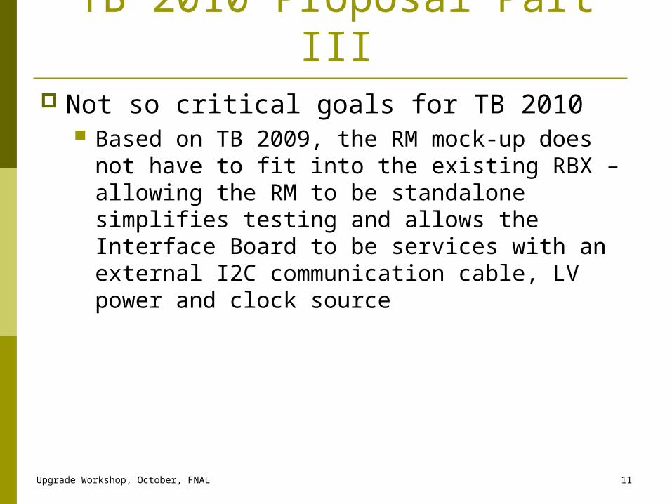
TB 2010 Proposal Part III Not so critical goals for TB 2010
Based on TB 2009, the RM mock-up does not have to fit into the existing RBX – allowing the RM to be standalone simplifies testing and allows the Interface Board to be services with an external I2C communication cable, LV power and clock source
Upgrade Workshop, October, FNAL 11
Summary Proposal and Mechanical Mock-up
provided for FPGA+ADC+InterfaceBoard card pack
Proposal limits card pack to 24-channels and no direct RBX interface requirement (RBX interface can be added later in the year)
Full-density EDU and control cards are still planned for TB 2010
Need to test whether switching layer configurations can be done and how
Upgrade Workshop, October, FNAL 12