Embed Size (px)
Citation preview

Plasmonic enhancement of Gold Nanoparticles in a microuidicbiochip
Ana Rita Trindade Antunes
Thesis to obtain the Master of Science Degree in
Biomedical Engineering
Supervisor(s): Doctor João Pedro Estrela Rodrigues Conde
Doctor João Garcia da Fonseca
Examination Committee
Chairperson: Prof. Luís Humberto Viseu Melo
Supervisor: Prof. João Pedro Estrela Rodrigues Conde
Member of the Committee:
Dr.Pedro Miguel Neves Ribeiro Paulo
Eng.Sandro Miguel Pinto Bordeira
March 2016

ii
The known is finite, the unknown infinite; intelectually we stand on as islet in the midst of an
illimitable ocean of inexplicability. Our business in every generation is to reclaim a little more land.
T. H. Huxley, 1887, from Cosmos
iii

iv

Agradecimentos
Finda esta longa jornada, cumprida com esforco, dedicacao e acima de tudo perseveranca, olho para tras
e surpreende-me ja terem decorrido sete anos. Foram sete anos de aprendizagem nao somente academica,
mas de enriquecimento pessoal: todos os que conheci ensinaram algo sobre mim mesma e sobre que pessoa
quererei ser.
Sendo a dissertacao o apogeu final do curso, nao poderei esquecer nem deixar de reconhecer a ajuda
inqualificavel de todos os intervenientes. Como tal, um primeiro profundo agradecimento ao meu orienta-
dor Professor Joao Pedro Conde, por melhorar o meu espırito crıtico sob as adversidades encontradas ao
longo das experiencias, bem como no incentivo de que qualquer trabalho pode ser sempre aperfeicoado.
Um genuıno obrigado ao meu co-orientador Dr. Joao Fonseca, pelo seu contributo nas varias sessoes na
Biosurfit. Nao poderei esquecer o Dr. Denis Roda dos Santos, Ruben Soares e Rui Pinto pela disponi-
bilidade que mostraram nas varias duvidas que os presenteei. Os meus sinceros agradecimentos ao Dr.
Narayanan Srinivasan por me ter dado nao so o seu tempo a discutir resultados e problemas encontrados,
mas tambem a sua amizade. Por fim, agradeco a todos os restantes colegas do INESC-MN, em particu-
lar a Giulia Petrucci, Joana Chim e Catarina Caneira pela amizade que criaram comigo ao longo deste
percurso, aliviando assim momentos menos bons.
Muitas pedras no caminho foram encontradas ao longo deste ano, guardei-as e vou construındo um
castelo. Esse castelo nao seria possıvel sem o apoio incondicional do meu Pai, que possibilitou toda
esta aventura e que me deu forca e motivacao nos momentos mais difıceis. Nao teria conseguido todo
este processo sem a incomparavel amizade e ajuda do Ruben Antonio, por acreditar em mim em alturas
que nem eu acreditava; nao teria conseguido sem a imensa amizade, dedicacao e preocupacao da Monica
Loureiro. Terei que reconhecer tambem a Monica Araujo, Andreia Oliveira e Susana Barroso pelo carinho,
ajuda e preciosas amizades. Todas me marcaram com excelentes memorias do curso. Sem elas, os
incontaveis almocos de boa disposicao que permitiram ver o bright side of your life em dias tristes nao
seriam possıveis.
Por fim, quero dedicar esta tese ao Dr.Carl Sagan, que atraves do seu livro Cosmos me relembrou o
quao pequenos somos, a paixao pela Ciencia e o deslumbre para com o desconhecido que nos rodeia.
v

vi

Resumo
As Nanopartıculas de Ouro exibem propriedades extraordinarias, diferentes do material comum, nas
quais propriedades opticas como o Localized Surface Plasmon Resonance (LSPR) sao dependentes da
sua dimensao e forma. Este trabalho apresenta a adsorcao de nanopartıculas esfericas estabilizadas
em citrato, de diametro 20 nm, num biochip microfluıdico, em que a aquisicao do LSPR foi realizada
atraves de fotodıodos e fotoconductores. Para a adsorcao de partıculas ocorrer nas superficies dos canais
microfluıdicos foi necessario a sua funcionalizacao com APTES durante 10 minutos, onde a interaccao
electrostatica entre as partıculas e o silano resultou num canal microfluıdico com total coloracao rosea.
A imobilizacao das nanopartıculas foi bem-sucedida utilizando um fluxo ininterrupto de 1 µL/min em
experiencias de 10, 20, 30 e 75 minutos de duracao, onde a funcionalizacao foi tambem realizada com
sucesso. O pico LSPR das nanopartıculas esfericas coloidais foi confirmado por Espectroscopia UV-Visıvel,
com 0.29 de absorvancia maxima registada a 520 nm. No sentido de detectar e avaliar o pico LSPR em
cada canal microfluıdico, utilizando fotodetectores, foi necessario acoplar no topo destes dispositivos,
barreiras de luz dispersa alinhadas com o biochip. As fotocorrentes obtidas dos dispositivos permitiram
a aquisicao do espectros, a fim de medir o pico LSPR, como tambem as fotocorrentes em funcao do
tempo. A diminuicao das fotocorrentes assinalada a 520 nm, em relacao aos valores obtidos com a
solucao de APTES no canal, apos 10 minutos da introducao das nanopartıculas sugere que a imobilizacao
nas superfıcies do canal tera sido profıcua. A acquisicao dos espectros foi realizada apos introduzir as
nanopartıculas no canal, com o objectivo de calcular os valores de absorvancia a cada comprimento
de onda. A 520 nm, o pico de absorvancia maximo foi obtido a 20, 30 e 75 minutos nas experiencias
de imobilizacao em fotodıodos e fotoconductores. No sentido de desenvolver um setup, acessıvel para
biodeteccao em sistemas Lab-on-a-Chip, os resultados aqui identificados asseguram futuras possibilidades
na monitorizacao em tempo real da interaccao entre nanopartıculas e moleculas biologicas, num robusto,
economico e reprodutıvel chip microfluıdico.
Palavras-chave: Nanopartıculas esfericas, LSPR, interaccao electrostatica, microfluıdica, fotodetec-
tores.
vii

viii
Abstract
Gold Nanoparticles exhibit extraordinary properties which are quite unlike those of bulk material, since
the optical properties, such as localized surface plasmon resonance (LSPR), are dependent on the dis-
played size and shape. This work presents the adsorption of citrate stabilized spherical gold nanoparticles
of 20 nm size in a microfluidic biochip, in which the LSPR acquisition was made using photodiodes and
photoconductors. For particle adsorption on channel surfaces, functionalization was successfully accom-
plished by flowing APTES inside the channel for 10 min, in which the electrostatic interaction between
the gold nanoparticless and the silane resulted in full-coloured red microfluidic channels. The immobiliza-
tion of the nanoparticles was successful flowing uninterruptedly at 1 µL/min for 20, 30 and 75 minutes,
in all experiments in which the surface silanization was also well accomplished. The LSPR peak of these
colloidal gold nanoparticles was confirmed by UV-Vis Spectroscopy, having maximum absorbance of 0.29
at 520 nm wavelength. To detect and evaluate the LSPR peak in each microchannel using photodetectors,
it was necessary to couple the photodetectors with light scattering barriers aligned below the microflu-
idic chip. The obtained photocurrents from both devices allowed the acquisition of current spectra, in
order to measure the LSPR peak, and the photocurrent measurement over time. The photocurrents
measurement at 520 nm decreased from initial value measured with APTES, after 10 min of flowing the
gold nanoparticles, suggesting that were successfully immobilized on the channel surfaces. The spectrum
acquisitions were performed after flowing the gold nanoparticles, in order to calculate absorbances values
at each wavelength. The absorbance value registed a peak at plasmonic wavelength of 520 nm, in 20, 30
and 75 min immobilization experiments, which was successfully calculated using photodiodes and pho-
toconductors. Towards the understanding and development of simple setup for biosensing purposes in a
Lab-on-a-Chip system, these findings show the possibilites in monitorizing in real-time gold nanoparticle
interaction with biological molecules, in a robust, low cost and easily fabricated microfluidic biochip.
Keywords: Spherical Gold Nanoparticles, LSPR, electrostatic interaction, microfluidics, photode-
tectors.
ix

x
Contents
Agradecimentos . . . . . . . . . . . . . . . . . . . . . . . . . . . . . . . . . . . . . . . . . . . . . v
Resumo . . . . . . . . . . . . . . . . . . . . . . . . . . . . . . . . . . . . . . . . . . . . . . . . . vii
Abstract . . . . . . . . . . . . . . . . . . . . . . . . . . . . . . . . . . . . . . . . . . . . . . . . . ix
List of Tables . . . . . . . . . . . . . . . . . . . . . . . . . . . . . . . . . . . . . . . . . . . . . . xiii
List of Figures . . . . . . . . . . . . . . . . . . . . . . . . . . . . . . . . . . . . . . . . . . . . . xv
Nomenclature . . . . . . . . . . . . . . . . . . . . . . . . . . . . . . . . . . . . . . . . . . . . . . xx
1 Introduction 1
1.1 Gold Nanoparticles: to plasmon or not to plasmon? . . . . . . . . . . . . . . . . . . . . . . 2
1.2 From Microfluidics to Biomicrofluidics . . . . . . . . . . . . . . . . . . . . . . . . . . . . . 6
1.3 Photodetectors . . . . . . . . . . . . . . . . . . . . . . . . . . . . . . . . . . . . . . . . . . 8
1.3.1 Theoretical concepts in semiconductors . . . . . . . . . . . . . . . . . . . . . . . . 8
1.3.2 Hydrogenated Amorphous Silicon p-i-n junction photodiodes . . . . . . . . . . . . 11
1.3.3 Intrinsic Hydrogenated Amorphous Silicon Photoconductors . . . . . . . . . . . . . 14
1.4 State-of-the-Art . . . . . . . . . . . . . . . . . . . . . . . . . . . . . . . . . . . . . . . . . . 15
1.5 Problem Description and Motivation . . . . . . . . . . . . . . . . . . . . . . . . . . . . . . 17
1.6 Thesis Outline . . . . . . . . . . . . . . . . . . . . . . . . . . . . . . . . . . . . . . . . . . 18
2 Experimental Methods 19
2.1 Moulds Fabrication . . . . . . . . . . . . . . . . . . . . . . . . . . . . . . . . . . . . . . . . 20
2.1.1 Surface Functionalization of PDMS Microchannels . . . . . . . . . . . . . . . . . . 21
2.2 Immobilization of Gold Nanoparticles (AuNPs) in a microfluidic channel . . . . . . . . . . 22
2.2.1 The role of Diffusion and Convection Phenomena in the immobilization step . . . . 22
2.3 Data Acquisition and Analysis . . . . . . . . . . . . . . . . . . . . . . . . . . . . . . . . . 25
3 Results and Discussion 31
3.1 Gold Nanoparticles: making their way into channels . . . . . . . . . . . . . . . . . . . . . 32
3.1.1 A PDMS/PDMS substrate experiment . . . . . . . . . . . . . . . . . . . . . . . . . 39
3.2 Scanning Electron Microscopy as a tool for insight . . . . . . . . . . . . . . . . . . . . . . 40
3.3 Localized Surface Plasmon Resonance Detection . . . . . . . . . . . . . . . . . . . . . . . 47
3.3.1 Localized Surface Plasmon Resonance (LSPR) detection in microfluidics using pho-
todiodes . . . . . . . . . . . . . . . . . . . . . . . . . . . . . . . . . . . . . . . . . . 47
xi

3.3.2 LSPR detection in microfluidics using photoconductors . . . . . . . . . . . . . . . 53
4 Conclusions and Future Challenges 61
Bibliography . . . . . . . . . . . . . . . . . . . . . . . . . . . . . . . . . . . . . . . . . . . . . . 67
4.1 References . . . . . . . . . . . . . . . . . . . . . . . . . . . . . . . . . . . . . . . . . . . . . 67
A Appendix 73
A.1 Photodiodes . . . . . . . . . . . . . . . . . . . . . . . . . . . . . . . . . . . . . . . . . . . . 74
A.2 Photoconductors . . . . . . . . . . . . . . . . . . . . . . . . . . . . . . . . . . . . . . . . . 77
A.3 Photodetectors Runsheets . . . . . . . . . . . . . . . . . . . . . . . . . . . . . . . . . . . . 82
xii

List of Tables
2.1 Different flow rates Q assumed and derived calculations. . . . . . . . . . . . . . . . . . . . 24
3.1 Experimental time calculated for each flow rate used. . . . . . . . . . . . . . . . . . . . . . 33
xiii

xiv
List of Figures
1.1 Gold Nanoparticles synthesized by the Turkevich method. . . . . . . . . . . . . . . . . . . 2
1.2 Effect of light interaction in a nanoparticle. . . . . . . . . . . . . . . . . . . . . . . . . . . 4
1.3 Different efficiencies corresponding to AuNPs sizes. . . . . . . . . . . . . . . . . . . . . . . 6
1.4 Silicon: energy levels splitting. . . . . . . . . . . . . . . . . . . . . . . . . . . . . . . . . . 9
1.5 Band diagram and Fermi-Dirac distribution function. . . . . . . . . . . . . . . . . . . . . . 10
1.6 2D representation of a dopped Silicon (Si) lattice. . . . . . . . . . . . . . . . . . . . . . . . 11
1.7 Representation of a p-i-n photodiode and associated energy bands. . . . . . . . . . . . . . 12
1.8 Quantum efficiency of a Si photodiode. [18] . . . . . . . . . . . . . . . . . . . . . . . . . . 14
1.9 A p-i-n photodiode responsivity compared with several quantum efficiencies of semicon-
ductors. [21] . . . . . . . . . . . . . . . . . . . . . . . . . . . . . . . . . . . . . . . . . . . . 14
1.10 Representation of photoconductor structure. . . . . . . . . . . . . . . . . . . . . . . . . . . 14
1.11 Comparison of gain and response times of distinctive photodetectors. . . . . . . . . . . . . 15
2.1 SU-8 mould used for PDMS channels. . . . . . . . . . . . . . . . . . . . . . . . . . . . . . 20
2.2 SU-8 mould resultant microfluidics channels and associated dimensions. . . . . . . . . . . 20
2.3 SU-8 mould on PMMA sheets used in photodetectors. . . . . . . . . . . . . . . . . . . . . 21
2.4 Shematic of PDMS channels fabrication. . . . . . . . . . . . . . . . . . . . . . . . . . . . . 21
2.5 Silanization of the channel surfaces. . . . . . . . . . . . . . . . . . . . . . . . . . . . . . . 22
2.6 Parameters of a microfluidic channel for transport analysis. Adapted from [47]. . . . . . . 23
2.7 Example of an area inside a microfluidic channel obtained by ImageJ. . . . . . . . . . . . 25
2.8 PDMS channel aligned with the photodetector dye. . . . . . . . . . . . . . . . . . . . . . . 26
2.9 Optical setup for the photodetector experiments. . . . . . . . . . . . . . . . . . . . . . . . 26
2.10 Current-Voltage (I-V) characterization values of dark photocurrent measured in photodiode. 27
2.11 I(t) characterization values of dark photocurrent measured in photodiode. . . . . . . . . . 27
2.12 The I-V values measured in dark environment of a used photoconductor. . . . . . . . . . . 27
2.13 The measured I(t) values in a dark environment of the same photoconductor. . . . . . . . 27
2.14 Aluminum (Al) barrier to exclude the scattered light. . . . . . . . . . . . . . . . . . . . . 28
2.15 Aluminum barrier fabrication scheme. . . . . . . . . . . . . . . . . . . . . . . . . . . . . . 28
2.16 Fabrication step scheme of second generation barrier: TiW . . . . . . . . . . . . . . . . . 29
2.17 Image of Al barriers fabricated. . . . . . . . . . . . . . . . . . . . . . . . . . . . . . . . . . 29
xv
2.18 Titanium Tungsten (TiW) barriers fabricated. . . . . . . . . . . . . . . . . . . . . . . . . . 29
3.1 Absorbance of original solution obtained by Ultraviolet-visible (UV-Vis) spectroscopy. . . 32
3.2 The incubation experiment image acquisitions, at 0 and 75 minutes. . . . . . . . . . . . . 34
3.3 PDMS sealed channels on glass were immobilization of AuNPs occured: a roseate channel
is visible. . . . . . . . . . . . . . . . . . . . . . . . . . . . . . . . . . . . . . . . . . . . . . 35
3.4 Olympus Microscope acquisitions of AuNPs immobilization assay for 75 min in micofluidic
channel, at Q = 1µL/min. . . . . . . . . . . . . . . . . . . . . . . . . . . . . . . . . . . . . 35
3.5 Olympus Microscope acquisitions of AuNPs immobilization assay in a microfluidic channel
at Q = 5µL/min, during 75min. . . . . . . . . . . . . . . . . . . . . . . . . . . . . . . . . 36
3.6 Transmittance values calculated through mean intensity values from ImageJ for two dif-
ferent flow rates Q. . . . . . . . . . . . . . . . . . . . . . . . . . . . . . . . . . . . . . . . . 36
3.7 Image acquisitions comparing two channel of different used flow rates. . . . . . . . . . . . 37
3.8 Control experiment, a channel without (3-Aminopropyl)triethoxysilane (APTES) surface
modification. . . . . . . . . . . . . . . . . . . . . . . . . . . . . . . . . . . . . . . . . . . . 37
3.9 Phosphate Buffered Saline (PBS) washing experiment in a previous AuNPs immobilization
assay channel. . . . . . . . . . . . . . . . . . . . . . . . . . . . . . . . . . . . . . . . . . . . 38
3.10 Comparison among three channels, where different flow rates were used: 0.05, 0.5 and 5
µL/min. . . . . . . . . . . . . . . . . . . . . . . . . . . . . . . . . . . . . . . . . . . . . . . 38
3.11 Transmittance values comparison of different AuNPs immobilization repetition experi-
ments using 1 µL/min. . . . . . . . . . . . . . . . . . . . . . . . . . . . . . . . . . . . . . 39
3.12 Immobilization of gold nanoparticles only on PDMS surfaces. . . . . . . . . . . . . . . . . 39
3.13 Transmittance values of assays perfomed in PDMS channel sealed on glass and on Poly(dimethylsiloxane)
(PDMS). . . . . . . . . . . . . . . . . . . . . . . . . . . . . . . . . . . . . . . . . . . . . . . 40
3.14 Acquisition of a full channel with AuNPs immobilized. . . . . . . . . . . . . . . . . . . . . 40
3.15 Channel with AuNPs immobilized used as sample for Scanning Electron Microscopy (SEM). 41
3.16 Pealing the PDMS channel of the glass substrate for SEM analysis. . . . . . . . . . . . . . 41
3.17 Top view of de-sealed channel acquisition in SEM. . . . . . . . . . . . . . . . . . . . . . . 42
3.18 SEM acquisition image of area 1, scale of 200 nm. . . . . . . . . . . . . . . . . . . . . . . . 42
3.19 SEM acquisition image of area 2, scale of 200 nm. . . . . . . . . . . . . . . . . . . . . . . 43
3.20 SEM acquisition of area 3, scale of 20 nm. . . . . . . . . . . . . . . . . . . . . . . . . . . . 43
3.21 SEM acquisitions of area 4, scale of 20 and 200 nm. . . . . . . . . . . . . . . . . . . . . . 44
3.22 SEM acquisitions of inlet and outlet zones. . . . . . . . . . . . . . . . . . . . . . . . . . . 44
3.23 Comparative results: SEM acquisition of 0.5 and 1 nM AuNPs. [48] . . . . . . . . . . . . 45
3.24 Comparative results: AFM acquisitions of immobilized AuNPs of two concentrations of
APTES. [50] . . . . . . . . . . . . . . . . . . . . . . . . . . . . . . . . . . . . . . . . . . . 46
3.25 APTES solution stability dependence on pH and temperature . . . . . . . . . . . . . . . . 47
3.26 Comparison between plasmon peak obtained by UV-Vis Spectroscopy and photodiode
acquisition. . . . . . . . . . . . . . . . . . . . . . . . . . . . . . . . . . . . . . . . . . . . . 48
xvi
3.27 Absorbances values calculated for a 30 min AuNPs immobilization. . . . . . . . . . . . . . 50
3.28 Channel on top of a photodiode dye using Al barrier. . . . . . . . . . . . . . . . . . . . . . 50
3.29 Absorbance spectrum acquired after 20 min of AuNPs immobilization. . . . . . . . . . . . 51
3.30 Absorbance spectrum acquired after 20 + 30 min of AuNPs immobilization. . . . . . . . . 51
3.31 Transmittance calculated over time acquired for 20 min of AuNPs immobilization. . . . . 52
3.32 Transmittance calculated over time acquired for 30 min of AuNPs immobilization. . . . . 52
3.33 Absorbance spectrum over 30 min of immobilization in photoconductor. . . . . . . . . . . 54
3.34 Calculated Transmittance over time of AuNPs immobilization in photoconductor. . . . . . 55
3.35 Absorbance spectrum of Bovine Serum Albumine (BSA) compared with AuNPs. . . . . . 56
3.36 Absorbance spectrum of 75 min immobilization acquired by photoconductor. . . . . . . . 56
3.37 Evolution of transmittance over 75 min of immobilization in photoconductor. . . . . . . . 57
3.38 TiW barrier aligned on top of photoconductor. . . . . . . . . . . . . . . . . . . . . . . . . 58
3.39 External Quantum Efficiency (EQE) dependency on bias voltage of a photoconductor. [57] 58
3.40 Responsivity of a-Si:H photoconductor and dependency on electrode spacing. [57] . . . . . 59
A.1 Figure of merit of photodiode using five different Neutral Density (ND) filters. . . . . . . 74
A.2 Photodiode photocurrent acquisition of black ink channel. . . . . . . . . . . . . . . . . . . 74
A.3 Typical photocurrents acquisition from 30 min immobilization of AuNPs. . . . . . . . . . 75
A.4 Spectra acquired of ink in two different microfluidic channels. . . . . . . . . . . . . . . . . 75
A.5 Hydrophobicity of the black ink inside a microfluidic channel. . . . . . . . . . . . . . . . . 76
A.6 Photocurrent spectrum acquisitions of the 20+30 min assay of AuNPs immobilization. . . 76
A.7 Comparison between photocurrents acquisition in photodiode, of each main step of the
20+30 min immobilization. . . . . . . . . . . . . . . . . . . . . . . . . . . . . . . . . . . . 77
A.8 Characterization: dark photocurrent of photoconductor. . . . . . . . . . . . . . . . . . . . 78
A.9 Characterization: ND3 yield photocurrent of photoconductor. . . . . . . . . . . . . . . . . 78
A.10 Characterization: ND3 yield photocurrent of black ink channel. . . . . . . . . . . . . . . . 78
A.11 Photocurrent spectrum acquisitions in photoconductor of 30 min immobilization assay. . . 79
A.12 Comparison between photocurrents acquisition in photoconductor, of each main step of 30
min immobilization. . . . . . . . . . . . . . . . . . . . . . . . . . . . . . . . . . . . . . . . 79
A.13 Photocurrents acquisitions of 75 min immobilization acquired by photoconductor. . . . . . 80
A.14 Comparison of photocurrents acquisitions of 75 min immobilization acquired by photocon-
ductor. . . . . . . . . . . . . . . . . . . . . . . . . . . . . . . . . . . . . . . . . . . . . . . . 80
A.15 Photocurrent spectrum acquisition of 75 min of AuNPs immobilization in photoconductor
using TiW barrier. . . . . . . . . . . . . . . . . . . . . . . . . . . . . . . . . . . . . . . . . 81
xvii

xviii

Nomenclature
Al Aluminum
As Arsenium
AFM Atomic Force Microscopy
APTES (3-Aminopropyl)triethoxysilane
AuNPs Gold Nanoparticles
a-Si:H Hydrogenated Amorphous Silicon
B Boron
B2H6 Diborane
Bi Bismuth
BSA Bovine Serum Albumine
DI-water Deionized water
EQE External Quantum Efficiency
Ge Germanium
H Hydrogen
Hg(II) Mercury
In Indium
ITO Indium-Tin-Oxide
I-V Current-Voltage
LoC Lab-on-a-Chip
LSPR Localized Surface Plasmon Resonance
N2 Nitrogen gas
ND Neutral Density
xix

NIR Near Infrared Reagion
P Phosphorus
PBS Phosphate Buffered Saline
PDMS Poly(dimethylsiloxane)
PeH Peclet number
PeS Shear Peclet number
PH3 Phosphine
PMMA Poly(methyl 2-methylpropenoate)
PoC Point-of-care
Re Reynolds number
RF-PECVD Radio-Frequency Plasma Enhanced Chemical Vapor Deposition
SEM Scanning Electron Microscopy
SERS Surface-enhanced Raman Spectroscopy
Si Silicon
SiH4 Silane gas
SiNx Silicon Nitride
SPR Surface Plasmon Resonance
TiW Titanium Tungsten
UV-O Ultraviolet Ozone
UV-Vis Ultraviolet-visible
xx

1Introduction
Contents
1.1 Gold Nanoparticles: to plasmon or not to plasmon? . . . . . . . . . . . . . 2
1.2 From Microfluidics to Biomicrofluidics . . . . . . . . . . . . . . . . . . . . . . 6
1.3 Photodetectors . . . . . . . . . . . . . . . . . . . . . . . . . . . . . . . . . . . . 8
1.4 State-of-the-Art . . . . . . . . . . . . . . . . . . . . . . . . . . . . . . . . . . . 15
1.5 Problem Description and Motivation . . . . . . . . . . . . . . . . . . . . . . 17
1.6 Thesis Outline . . . . . . . . . . . . . . . . . . . . . . . . . . . . . . . . . . . . 18
1
1.1 Gold Nanoparticles: to plasmon or not to plasmon?
Gold and iron at the present day,
as in ancient times, are the rulers
of the world.
William Whewell, 1851
Through ages, Man has mastered the art of extracting and crafting gold for its own purposes, from
sacred symbols, monarchists purposes, as well as decoration in ceramics or glass, to medicine. The use
of gold in therapeutics dated back to thousand of years ago in India and later in the Medieval Europe,
due to its intrinsic characteristics: non-toxic, non-irritating and resistant to chemical corrosion.
In the present chapter, the nanoscale properties of gold particles are discussed. The following charac-
terization attempts to demonstrate, to several readers, the physics and the optical advantages behind
this material, as well as the broad applicability, impossible to report in full extension. Gold Nanoparti-
cles (AuNPs) possess unique optical, physical and electronic properties that enables applications in diverse
fields. These properties are totally dependent on size and shape, these key parameters are related to light
scattering and surface chemical activity; therefore the production through different methods should be
systematic and controlled over morphology and composition. There are well-known liquid-phase syn-
thetic methods performed by the reduction of gold percursors introduced in organic or aqueous media,
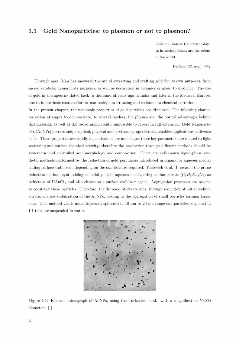
adding surface stabilizers, depending on the size features required. Turkevich et al. [1] created the prime
reduction method, synthesizing colloidal gold, in aqueous media, using sodium citrate (C6H5Na3O7) as
reductant of HAuCl4 and also citrate as a surface stabilizer agent. Aggregation processes are needed
to construct these particles. Therefore, the decrease of citrate ions, through reduction of initial sodium
citrate, enables stabilization of the AuNPs, leading to the aggregation of small particles forming larger
ones. This method yields monodispersed, spherical of 10 nm to 20 nm range-size particles, depicted in
1.1 that are suspended in water.
Figure 1.1: Electron micrograph of AuNPs, using the Turkevich et al. with a magnification 50,000
diameters. [1]
2
As mentioned previously, size and shape are the main determinants for the physical occurances, by
which optical properties are influenced. AuNPs can be classified by size, and, in this work, 20 nm di-
ameter particles were used and categorized to a defined class range of 10-300 nm . [2] In this size scope,
it is designated by a plasmonic crystal whose more interesting properties are Localized Surface Plasmon
Resonance (LSPR) and Surface Plasmon Resonance (SPR), which will be described below.
The physics behind AuNPs can be described by analysing the interaction between an electromagnetic
wave and a metallic surface. In the visible range, an incident electromagnetic wave on a metal does not
penetrate further than the designated skin depth (or penetration depth), where for example a 500 nm
wavelength light beam would have a penetration depth of 20 nm. [2] Penetration depth is considered to
be a measure of electomagnetic wave decay inside a material, which can be described by Beer-Lambert
Law. Therefore, the penetration depth depends greatly on the incident wavelength. When a light beam
is incident on a surface of a metal, it creates a thin sheet of polarization with penetration depth thickness
at the surface, where the electrons in the conduction band of gold act as free polarized particles, with
certain detachment from the nucleus. This occurs in two specific cases, first in systems where the size
of metal structures have the same order magnitude of the penetration depth and second in the case of
a flat theoretically infinite surface. Concerning the two cases described above, it is needed to clarify the
difference between LSPR and SPR.
In respect to the first case, where the size of the AuNPs is inferior to the incident beam’s wavelength
and in many cases it is also smaller than the penetration depth, a particular phenomena occurs on the
oscillation of charges. The electric field from the incident electromagnetic wave attains the free electrons
from the valence band, polarizing the whole surface of the nanoparticle, since the particle size is the
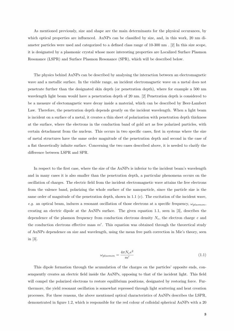
same order of magnitude of the penetration depth, shown in 1.1 (c). The excitation of the incident wave,
e.g. an optical beam, induces a resonant oscillation of those electrons at a specific frequency, ωplasmon,
creating an electric dipole at the AuNPs surface. The given equation 1.1, seen in [3], describes the
dependence of the plasmon frequency from conduction electrons density Ne, the electron charge e and
the conduction electrons effective mass m′. This equation was obtained through the theoretical study
of AuNPs dependence on size and wavelength, using the mean free path correction in Mie’s theory, seen
in [3].
ωplasmon =4πNee
2
m′(1.1)
This dipole formation through the acumulation of the charges on the particles’ opposite ends, con-
senquently creates an electric field inside the AuNPs, opposing to that of the incident light. This field
will compel the polarized electrons to restore equilibrium positions, designated by restoring force. Fur-
thermore, the yield resonant oscillation is somewhat repressed through light scattering and heat creation
processes. For these reasons, the above mentioned optical characteristics of AuNPs describes the LSPR,
demonstrated in figure 1.2, which is responsible for the red colour of colloidal spherical AuNPs with a 20
3
nm diameter size.
Figure 1.2: Schematic of the light interaction with a nanoparticle, resulting in the creation of an electric
field (c). Through the collective oscillations, cross-sections of absorption and scattering are originated.
The LSPR at the plasmon wavelength for different size ranges are presented in (h), (i). Adapted image
from [4].
The light incident of nanoparticles depending on size can be absorbed or scattered. In order to analyze
the efficiency of such processes, it is necessary to characterize both in cross-sections, for absorption and
elastic scattering, so that the sum of the two processes causes light attenuation, characterized by the
extinction cross-section. According to the simplified scattering model, applied to small and homogeneous
spherical particles, where a first order in multipole expansion in Mie theory is used to calculate the
extinction cross section σext and scattering cross-section σscatt. To derive the light intensity of a wave
being absorbed, the σabs relates the three cross-sections described in equation 1.2, seen in [2] .
σabs = σext − σscatt (1.2)
AuNPs of 20 nm size, when isolated and in colloidal form, display a predominant absorption cross-
section, with plasmon resonance peak at 520 nm wavelength, causing the extinction of respective green
wavelengths, although transmission of red colours arise. When agglomerated, the plasmon resonance
shifts for longer wavelengths and the peak itself is broadened, therefore the red colour is consequently
absorbed.
According to [2], the fundamental properties of LSPR can be described:
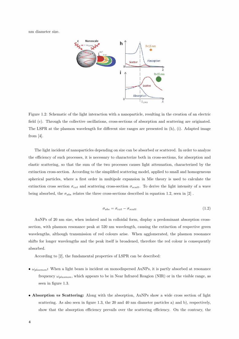
• ωplasmon: When a light beam is incident on monodispersed AuNPs, it is partly absorbed at resonance
frequency ωplasmon, which appears to be in Near Infrared Reagion (NIR) or in the visible range, as
seen in figure 1.3.
• Absorption vs Scattering: Along with the absorption, AuNPs show a wide cross section of light
scattering. As also seen in figure 1.3, the 20 and 40 nm diameter particles a) and b), respectively,
show that the absorption efficiency prevails over the scattering efficiency. On the contrary, the
4
scattering efficiency is visible for the 80 nm diameter particle. Therefore, the increase in particle
size implies dominance of scattering over absorption.
• towards LSPR Biosensing: The possibilities of using AuNPs widens as biosensing plataforms, in
colorimetric assays using Lab-on-a-Chip (LoC) systems, since the position of LSPR peak, in ex-
tinction spectrum is deeply influenced by the surrounding medium refractive index. The LSPR
is extremely sensitive to the surrounding medium, whereas the conduction electrons frequency of
oscillation is most dependent on the external dielectric constant thereby related to the refractive
index. In focus, the resonance peak is shifted to longer wavelengths, as the refractive index (n)
increases, as illustrated in equation 1.3, from [5]. This equation is verified in cases where the change
in refractive index is due to the absorption of a certain layer in the surroundings of the nanopar-
ticles, specifically where the layer’s thickness is inferior to the electric field decay. The shift of
plasmon resonance peak is also directly dependent on the responsiveness m of the nanoparticles.
This finds purpose in biosensing for targeted molecules, in which if a target binds specifically to
the AuNPs, it leads to a higher average refractive index in the neighbouring medium, causing the
LSPR to red shift. The increase of absorption and scattering processes, utterly dependent upon
size, are of major importance in the biosensing and enhancement on sensitivity processes, thereby
a significant interest in developing a highly sensitive biological and chemical sensors is based on
these nanosystems.
4 (λmax) = m(nA − nE)[1− e−2dld ] (1.3)
Being nA the refractive index of the adsorbate layer, nE the refractive index of the particle envi-
ronment, d the thickness of the adsorbate layer and ld is the electric field decay length.
The efficiencies demonstrated in figure 1.3 were calculated from Mie theory for three particle sizes.
Moreover, in 1908, Gustav Mie [6] solved the Maxwell’s equations and calculated an analytical and exact
solution of the surface plasmon of spherical nanoparticles and the intensity of light absorption, using the
assumption that the particles would be distant enough, so that the electric field created among them
would not affect all individually. This theory postulates that when the size of the nanoparticle is smaller
that the incident light’s wavelength, the electric field of the nanoparticle is spatially constant, but has
phase variable which is dependent on time. This so called dipolar approximation theory is valid for
particles with size inferior to 60 nm.
5
Figure 1.3: The different efficiencies: green line represents exctintion, red dashed line represents absorp-
tion and black dots represent scattering. Where a) 20 nm, b) 40 nm and c) 80 nm diameters. [7]
The processes of absorption and scattering are of main importance to the present work. As formerly
pointed regarding the absorption efficiency, it theoretically describes the geometrical section of an ideal
opaque particle, which absorbs the equal number of photons as the one particle in study. Therefore, the
absorption efficiency is handed out by its absorption cross section. [8] Besides absorption, as light interacts
with AuNPs it can also be scattered, so a scattering cross section can be defined as the geometrical section
of an ideal scattering particle having the same efficiency as the particle in study. Finally, the extinction
cross section can be defined as the sum of the absorption and scattering cross section, representing the
ability of a particle to extract photons from incident light through both processes. [8]
As specified above, another interesting property is the SPR. When an electromagnetic wave is incident
between an infinite flat metal surface and an insulator, the two having different dielectric functions, a
surface wave is created and it is restrained close to the interface between them. The surface wave is
named polariton, a charge density with a longitudinal direction, opposed to the transversal direction of
the incident wave. Since these two wave couple, when the incident beam possess a given angle, capable
to excite, a surface plasmon wave is arised. Considering that SPR is only seen on flat planes of infinite
extension, this topic falls out of the scope in this work.
1.2 From Microfluidics to Biomicrofluidics
The Microfluidics field rose from two different science fields: analytical chemistry and microfabrication.
The urgency of solving both chemically and biochemically relevant problems led to the increased usage
and development of microdevices. Nowadays, the scope of microfluidics is seen in fields such as bio-
chemistry, biology and bioengineering, giving birth to the claimed Biomicrofluidics. This field hinges on
transport phenomena and flow physics in nano and micro length scale systems, operating and controlling
small volumes of gases or liquid, the latter from fento-litre to micro-litre. Hence offering different appli-
cations through varied geometric shapes of small channels. In this section, the fundamental aspects of
fluids flowing over microscopic scales, along with its mechanisms and implications, will be presented.
The Navier-Stokes equations are a common tool used to understand the behaviour of a fluid inside a
microfluidic set, using the fluid’s characteristics such as velocity, pressure, density and dynamic viscosity.
6
The terms of the expressions that constitute the equation represent the several forces in which the fluid
is exposed to: inertial, pressure, viscous and external forces. The underlined calculations is build upon
a continuum hypothesis, which states that there are enough molecules to establish statistical properties
when using small volumes. [9] Then, if the fluid is assigned to as a continuum, these equations are
accurately aplied to liquids in microsystems, concerning that the physical dimension of the channel(L)
is much wider than fluid’s molecules mean free path (λ), represented by the Knudsen number given in
equation 1.4. [10]
Kn =λ
L(1.4)
The mean free path is the average linear displacement between two moving molecules that collide
and thereby, change directions. These collisions are naturally associated with temperature, as can be
seen in gases and liquids. [9] Considering that the mean free path is smaller that the characteristic size
of a channel in liquids, the continuum hypothesis is still viable. The simplification of the Navier-Stokes
equations can be accomplished depending on flow’s regime, which can be defined by a non-dimensional
value, Reynolds number, according to equation 1.5. [10]
Re =ULρ0µ
(1.5)
Where U is the characteristic velocity, L is length of the flow, ρ0 is the constant fluid’s density and
µ is the constant kinematic viscosity of the fluid. It is to be noticed that the Reynolds number (Re) is
not a property of the fluid but it is a parameter that combines the fluid and geometric properties. The
equation 1.5 represents the ratio of the inertial forces over the viscous forces, measuring the turbulence
of the flow. If Re is low, Re ≤ 1, the interaction between the viscous forces amidst the wall and the fluid
is intensified, with no turbulences and vortices occuring, so the flow is laminar; if Re is higher, the flow
is turbulent. Commonly in microfluidics, specifically LoC, laminar flow is the most present regime (if
the application of interest does not require larger channels or higher speeds). By assumption, if U is less
than cm.s−1 and L in the range order of µm, then the Re ≤ 0.1. [11]
The molecules in a gas or liquid have a peculiar erratic movement, a Brownian motion behaviour,
which is parallel in macromolecules and microparticles, which behaviour can be described analogously.
The conception of Diffusion is built upon Brownian theory, where a initially confined group of particles
of a certain volume starts erratic movements over time and are continuously dispersed in a buffer liquid.
The presented equation 2.1 is based on the preceding continuum hypothesis. [10]
D =KBT
6πµRH(1.6)
Where KB is the Boltzmann Constant, T the absolute temperature in K, µ the viscosity of the
solvent fluid and RH the hydrodynamic radius of solute particles. The accepted Diffusion coefficient for
commonly tested biomolecule analytes is approximately 10−10 to 10−9 m2/s. [10] In the process of particle
spreading, a diffusive flux JD can be analysed. According to Flick’s Law in equation 1.7, the number of
7
particles crossing a unit surface, in time t, is in fact proportional to the gradient of concentration (with a
negative constant of proportion, since diffusion occurs reversed from gradient concentration) and to the
Diffusion Coefficient. [10]
JD = −D5c (1.7)
Inside a confinement, the particles of a fluid are performing diffusion, but are also creating the advec-
tion of a velocity field along the fluid. The competition between advection and diffusion is the mechanism
behind several mass and chemical transports. In order to evaluate the predominance of advection in re-
lation to diffusion, the Peclet, PeH , number was defined, as seen in equation 2.2. [11]
PeH =Ul
D(1.8)
Polymeric material, such as Poly(dimethylsiloxane) (PDMS), is commonly used for LoC purposes.
The usual microfabrication technique applied is Soft Lithography, being a low cost and a fast procedure.
There are different techniques that are included in Soft Lithography processes, sharing the general proto-
col of fabrication, although they differ in the way that a polymer stamp is used to reproduce its form. [12]
PDMS has been one of the leading choices to fabricate microchannels and has the potential to integrate
valves, mixers and pumps on-chip. These contributions have settled the foundations of micro total anal-
ysis systems (µTAS). As an elastomer, PDMS presents characteristics that are useful and advantageous
for biological assays, since it is chemically inert, has no swelling properties in humid environments, is
biocompatible and has a structural compliance when in contact with large area surfaces. Moreover, this
polymer possess good permeability to gases, is homogeneous, isotropic and is compatible with several
optical detection systems, since it is optically transparent from 300 nm to IR range. After the fabrication
process of PDMS conformations needed, surface modification developments take place. The hydrophobic
nature of this material it is prone to non-specific protein adsorption, thus it is necessary to perform
surface treatment in order to minimize these occurrences. Surface treatments are highly dependent of the
biological goals, for that purpose some of the most common techniques are Ultraviolet Ozone (UV-O),
Oxigen Plasma or Corona Discharge, as seen in [13].
1.3 Photodetectors
1.3.1 Theoretical concepts in semiconductors
Photodetectors are made of semiconductor materials that detect incident light by photon absorption
and originate a flow current, proportional to the initial light intensity. To address photodiodes operation
modes, it is essential to elucidate theoretical concepts on semiconductor materials and quantum mechanics
principles.
Silicon (Si) has four valence electrons that establish covalent bonds with surrounding silicon atoms
when creating a lattice. A pure silicon crystal behaves as an insulator, since the outer electrons are all
involved in covalent bonds, with no free electrons to conduct electric current. Although these atoms
8
bond covalently, the bonds are substantially weaker than carbon-carbon ones, present in insulators such
as glass, diamonds and polymers. The excitation energy that electrons need to surpass, to migrate from
the valence band to the conduction band, is called the forbidden gap (Eg), in which its values define
whether a material is an insulator, a semiconductor or a conductor. If the Eg is large, then the electron
energy from an applied electric field will not be sufficient for an electron in the valence band to enter
the conduction band. Thus, this electron would not be freed and no current would flow, as it is seen in
insulators.
In the case of semiconductors, although Eg is smaller, they are not electrically conductive in low
temperatures. Yet, through thermal excitation some electrons involved in covalent bonds would become
free and become conduction electrons carrying enough energy to overwhelm the forbidden gap. In oppo-
sition to semiconductors, the forbidden gap is inexistent in conductors, due to the overlap between the
valence and conduction bands. [14] As pointed out, thermal excitation leads to electric conductivity in
semiconductors. When temperature increases, Eg tends to decrease, since the interatomic distances are
greater, causing a reduction in the average potential. [15]
The formation of energy bands is intimately related with discrete electronic states and associated
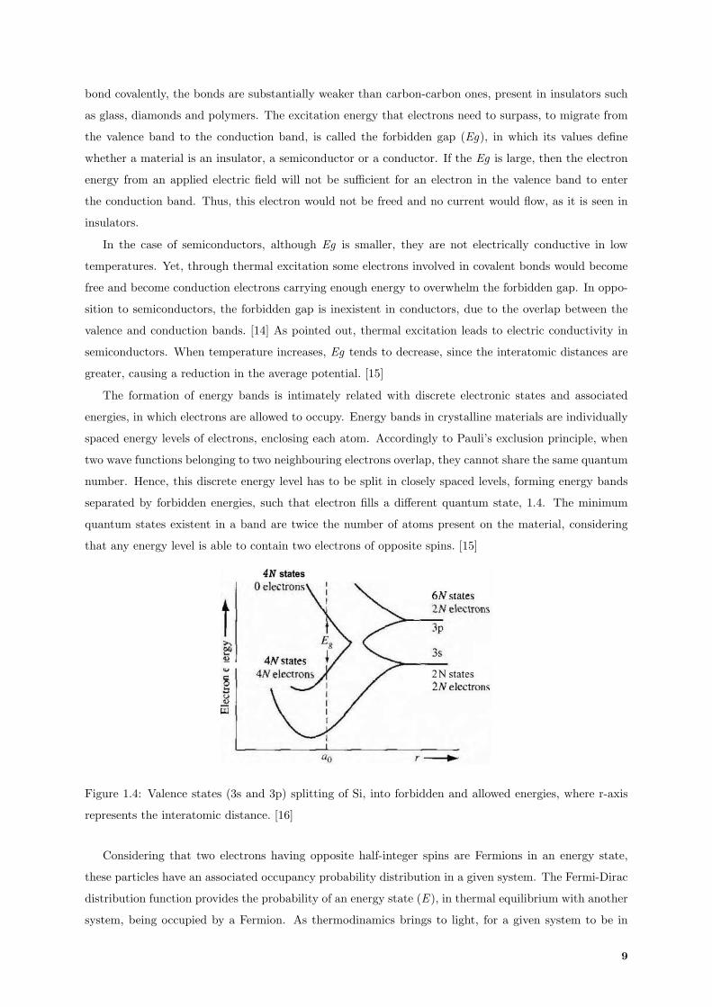
energies, in which electrons are allowed to occupy. Energy bands in crystalline materials are individually
spaced energy levels of electrons, enclosing each atom. Accordingly to Pauli’s exclusion principle, when
two wave functions belonging to two neighbouring electrons overlap, they cannot share the same quantum
number. Hence, this discrete energy level has to be split in closely spaced levels, forming energy bands
separated by forbidden energies, such that electron fills a different quantum state, 1.4. The minimum
quantum states existent in a band are twice the number of atoms present on the material, considering
that any energy level is able to contain two electrons of opposite spins. [15]
Figure 1.4: Valence states (3s and 3p) splitting of Si, into forbidden and allowed energies, where r-axis
represents the interatomic distance. [16]
Considering that two electrons having opposite half-integer spins are Fermions in an energy state,
these particles have an associated occupancy probability distribution in a given system. The Fermi-Dirac
distribution function provides the probability of an energy state (E ), in thermal equilibrium with another
system, being occupied by a Fermion. As thermodinamics brings to light, for a given system to be in
9
thermal equilibrium, it must have the lowest energy configuration when subjected to thermal agitation.
For that reason, Fermions fill first the lower energy states and higher ones are filled next. When the system
is at absolute zero, 0 K, Fermions will fill the states to a maximum energy level called the Fermi energy
level (EF ), with no higher energy states filled. The Fermi energy level remains constant throughout the
system, as long as thermal equilibrium is present. [15]
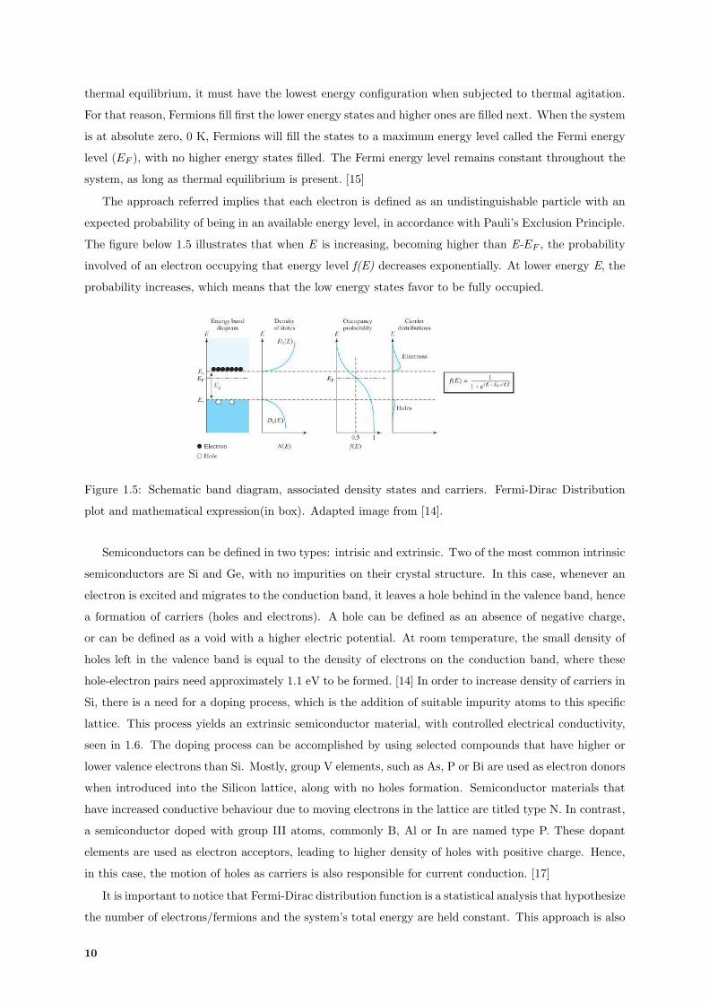
The approach referred implies that each electron is defined as an undistinguishable particle with an
expected probability of being in an available energy level, in accordance with Pauli’s Exclusion Principle.
The figure below 1.5 illustrates that when E is increasing, becoming higher than E-EF , the probability
involved of an electron occupying that energy level f(E) decreases exponentially. At lower energy E, the
probability increases, which means that the low energy states favor to be fully occupied.
Figure 1.5: Schematic band diagram, associated density states and carriers. Fermi-Dirac Distribution
plot and mathematical expression(in box). Adapted image from [14].
Semiconductors can be defined in two types: intrisic and extrinsic. Two of the most common intrinsic
semiconductors are Si and Ge, with no impurities on their crystal structure. In this case, whenever an
electron is excited and migrates to the conduction band, it leaves a hole behind in the valence band, hence
a formation of carriers (holes and electrons). A hole can be defined as an absence of negative charge,
or can be defined as a void with a higher electric potential. At room temperature, the small density of
holes left in the valence band is equal to the density of electrons on the conduction band, where these
hole-electron pairs need approximately 1.1 eV to be formed. [14] In order to increase density of carriers in
Si, there is a need for a doping process, which is the addition of suitable impurity atoms to this specific
lattice. This process yields an extrinsic semiconductor material, with controlled electrical conductivity,
seen in 1.6. The doping process can be accomplished by using selected compounds that have higher or
lower valence electrons than Si. Mostly, group V elements, such as As, P or Bi are used as electron donors
when introduced into the Silicon lattice, along with no holes formation. Semiconductor materials that
have increased conductive behaviour due to moving electrons in the lattice are titled type N. In contrast,
a semiconductor doped with group III atoms, commonly B, Al or In are named type P. These dopant
elements are used as electron acceptors, leading to higher density of holes with positive charge. Hence,
in this case, the motion of holes as carriers is also responsible for current conduction. [17]
It is important to notice that Fermi-Dirac distribution function is a statistical analysis that hypothesize
the number of electrons/fermions and the system’s total energy are held constant. This approach is also
10
applied on impurities, present in semiconductors materials. Moreover, it is possible to define the Fermi
level in both types of doped semiconductors. The Fermi level on a n-doped semiconductor is localized
near the conduction band, as for the p-doped semiconductor is localized near the valence band.
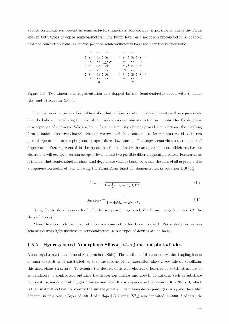
Figure 1.6: Two-dimensional representation of a dopped lattice. Semiconductor doped with a) donor
(As) and b) acceptor (B). [14]
In doped semiconductors, Fermi-Dirac distribution function of impurities contrasts with one previously
described above, considering the possible and unknown quantum states that are implied for the donation
or acceptance of electrons. When a donor from an impurity element provides an electron, the resulting
form is ionized (positive charge), with an energy level that contains an electron that could be in two
possible quantum states (spin pointing upwards or downwards). This aspect contributes to the one-half
degeneration factor presented in the equation 1.9 [15]. As for the acceptor element, which receives an
electron, it will occupy a certain acceptor level in also two possible different quantum states. Furthermore,
it is usual that semiconductors show dual degenerate valence band, by which the sum of all aspects yields
a degeneration factor of four affecting the Fermi-Dirac function, demonstrated in equation 1.10 [15].
fdonor =1
1 + 12e
(Ed − EF )/kT(1.9)
facceptor =1
1 + 4e(Ea − EF )/kT(1.10)
Being Ed the donor energy level, Ea the acceptor energy level, EF Fermi energy level and kT the
thermal energy.
Along this topic, electron excitation in semiconductors has been reviewed. Particularly, in carriers
generation from light incident on semiconductors in two types of devices are on focus.
1.3.2 Hydrogenated Amorphous Silicon p-i-n junction photodiodes
A non-regular crystalline form of Si is seen in (a-Si:H). The addition of H atoms allows the dangling bonds
of amorphous Si to be passivated, so that the process of hydrogenation plays a key role on stabilizing
this amorphous structure. To acquire the desired optic and electronic features of a-Si:H structure, it
is mandatory to control and optimize the deposition process and growth conditions, such as substrate
temperature, gas composition, gas pressure and flow. It also depends on the power of RF-PECVD, which
is the usual method used to control the surface growth. The plasma decomposes gas SiH4 and the added
dopants, in this case, a layer of 100 A of n-doped Si (using PH3) was deposited, a 5000 A of intrinsic
11
Si layer and 100 A of p-doped Si, using B2H6 were also deposited. Hence, the intrisic layer is wider and
has less doping. In addition, a 2000 A layer of ITO for top contact deposition was performed also, as a
anti-reflection coating. As referred above, p-i-n photodiode is a structure of an intrinsic region between
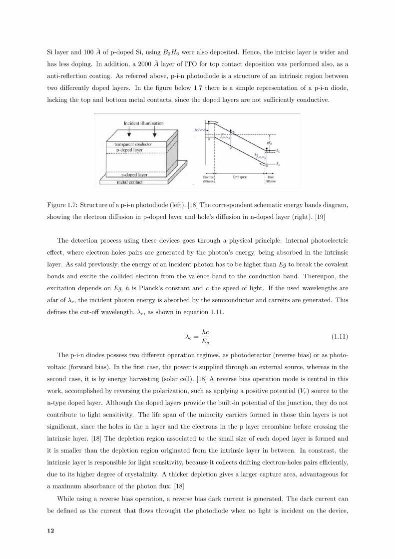
two differently doped layers. In the figure below 1.7 there is a simple representation of a p-i-n diode,
lacking the top and bottom metal contacts, since the doped layers are not sufficiently conductive.
Figure 1.7: Structure of a p-i-n photodiode (left). [18] The correspondent schematic energy bands diagram,
showing the electron diffusion in p-doped layer and hole’s diffusion in n-doped layer (right). [19]
The detection process using these devices goes through a physical principle: internal photoelectric
effect, where electron-holes pairs are generated by the photon’s energy, being absorbed in the intrinsic
layer. As said previously, the energy of an incident photon has to be higher than Eg to break the covalent
bonds and excite the collided electron from the valence band to the conduction band. Thereupon, the
excitation depends on Eg, h is Planck’s constant and c the speed of light. If the used wavelengths are
afar of λc, the incident photon energy is absorbed by the semiconductor and carreirs are generated. This
defines the cut-off wavelength, λc, as shown in equation 1.11.
λc =hc
Eg(1.11)
The p-i-n diodes possess two different operation regimes, as photodetector (reverse bias) or as photo-
voltaic (forward bias). In the first case, the power is supplied through an external source, whereas in the
second case, it is by energy harvesting (solar cell). [18] A reverse bias operation mode is central in this
work, accomplished by reversing the polarization, such as applying a positive potential (Vr) source to the
n-type doped layer. Although the doped layers provide the built-in potential of the junction, they do not
contribute to light sensitivity. The life span of the minority carriers formed in those thin layers is not
significant, since the holes in the n layer and the electrons in the p layer recombine before crossing the
intrinsic layer. [18] The depletion region associated to the small size of each doped layer is formed and
it is smaller than the depletion region originated from the intrinsic layer in between. In constrast, the
intrinsic layer is responsible for light sensitivity, because it collects drifting electron-holes pairs efficiently,
due to its higher degree of crystalinity. A thicker depletion gives a larger capture area, advantageous for
a maximum absorbance of the photon flux. [18]
While using a reverse bias operation, a reverse bias dark current is generated. The dark current can
be defined as the current that flows throught the photodiode when no light is incident on the device,
12
resulting in a noise source in this operation mode, therefore this current is controlled by the internal
energy barrier. The resultant dark current, or leakage current, is a key parameter in a diode performance
evaluation. A highly efficient photodiode is related to the lowest dark current possible, which is only
accomplished by having thermal generation current in a full depleted diode. The bulk thermal current
is a result of electron excitation from the valence band to a defect state that is singly occupied, due to
thermal energy. This major contributor to the dark current can be reduced by decreasing the deffect’s
density and by increasing the Eg. In addition, the doped contact injection and edge leakage of the
component may be also contributing factors to the dark current. [20]
Besides, under reverse bias, a photocurrent Iph is created resulting from light exposure, throught
the electron-holes pairs being generated in the intrinsic layer and drifted across it by the electrical field.
The photocurrent is directly proportional to the quantum effiency, ηQE , given by the ratio between the
number of electron-hole carrier pairs generated per incident and absorbed photon with energy hv, shown
in the equation 1.12. [21]
ηQE =Iph/q
Pin/hv(1.12)
Where Iph is the photocurrent, q the elementary charge, Pin the optical power at wavelength λ, h
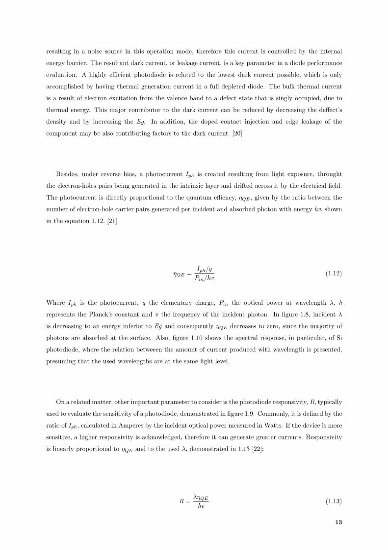
represents the Planck’s constant and v the frequency of the incident photon. In figure 1.8, incident λ
is decreasing to an energy inferior to Eg and consequently ηQE decreases to zero, since the majority of
photons are absorbed at the surface. Also, figure 1.10 shows the spectral response, in particular, of Si
photodiode, where the relation betweeen the amount of current produced with wavelength is presented,
presuming that the used wavelengths are at the same light level.
On a related matter, other important parameter to consider is the photodiode responsivity, R, typically
used to evaluate the sensitivity of a photodiode, demonstrated in figure 1.9. Commonly, it is defined by the
ratio of Iph, calculated in Amperes by the incident optical power measured in Watts. If the device is more
sensitive, a higher responsivity is acknowledged, therefore it can generate greater currents. Responsivity
is linearly proportional to ηQE and to the used λ, demonstrated in 1.13 [22]:
R =ληQE
hv(1.13)
13
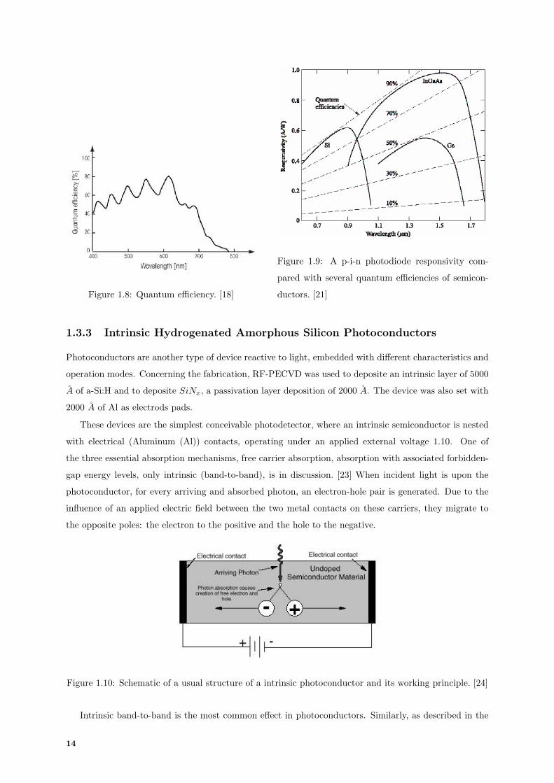
Figure 1.8: Quantum efficiency. [18]
Figure 1.9: A p-i-n photodiode responsivity com-
pared with several quantum efficiencies of semicon-
ductors. [21]
1.3.3 Intrinsic Hydrogenated Amorphous Silicon Photoconductors
Photoconductors are another type of device reactive to light, embedded with different characteristics and
operation modes. Concerning the fabrication, RF-PECVD was used to deposite an intrinsic layer of 5000
A of a-Si:H and to deposite SiNx, a passivation layer deposition of 2000 A. The device was also set with
2000 A of Al as electrods pads.
These devices are the simplest conceivable photodetector, where an intrinsic semiconductor is nested
with electrical (Aluminum (Al)) contacts, operating under an applied external voltage 1.10. One of
the three essential absorption mechanisms, free carrier absorption, absorption with associated forbidden-
gap energy levels, only intrinsic (band-to-band), is in discussion. [23] When incident light is upon the
photoconductor, for every arriving and absorbed photon, an electron-hole pair is generated. Due to the
influence of an applied electric field between the two metal contacts on these carriers, they migrate to
the opposite poles: the electron to the positive and the hole to the negative.
Figure 1.10: Schematic of a usual structure of a intrinsic photoconductor and its working principle. [24]
Intrinsic band-to-band is the most common effect in photoconductors. Similarly, as described in the
14
prior topics, the hole-pair formation follows the same principle, as to intrinsic layer in photodiodes. An
incident photon must comprise sufficient energy to excite the electron from the valence band, therefore
the incident light should carry a certain wavelength to exceed the forbidden gap energy, seen in 1.11.
According to the literature, an intrinsic Si photoconductor has a forbidden gap energy of 1.12 eV, with
a typical operating range of 500 to 900 nm. [23]
As mentioned, the movement of the carriers to the opposite poles in response to an applied voltage
creates a photocurrent, which is proportional to the incident photon flux, φ. Thereby, the increase of
conductivity is a result of increased number of carriers. [25] If the number of carriers reaching the contact
pads are taken into consideration in terms of time (seconds), a parameter for evaluating the detector’s
perfomance is considered. For each carrier migrating between the poles per second and for each photon
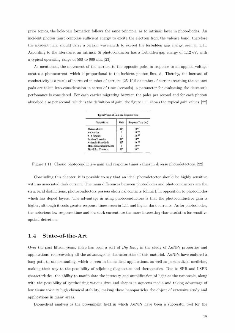
absorbed also per second, which is the definition of gain, the figure 1.11 shows the typical gain values. [22]
Figure 1.11: Classic photoconductive gain and response times values in diverse photodetectors. [22]
Concluding this chapter, it is possible to say that an ideal photodetector should be highly sensitive
with no associated dark current. The main differences between photodiodes and photoconductors are the
structural distinctions, photoconductors possess electrical contacts (ohmic), in opposition to photodiodes
which has doped layers. The advantage in using photoconductors is that the photoconductive gain is
higher, although it costs greater response times, seen in 1.11 and higher dark currents. As for photodiodes,
the notorious low response time and low dark current are the more interesting characteristics for sensitive
optical detection.
1.4 State-of-the-Art
Over the past fifteen years, there has been a sort of Big Bang in the study of AuNPs properties and
applications, rediscovering all the advantageous characteristics of this material. AuNPs have endured a
long path to understanding, which is seen in biomedical applications, as well as personalized medicine,
making their way to the possibility of adjoining diagnostics and therapeutics. Due to SPR and LSPR
characteristics, the ability to manipulate the intensity and amplification of light at the nanoscale, along
with the possibility of synthesizing various sizes and shapes in aqueous media and taking advantage of
low tissue toxicity high chemical stability, making these nanoparticles the object of extensive study and
applications in many areas.
Biomedical analysis is the proeminent field in which AuNPs have been a successful tool for the
15
diversed applications. In behalf of some properties owing to the individual interaction at the same
scale, the size of small AuNPs can be in the order of magnitude of some biological entities such as
DNA chains, cells, bacteria and even viruses. Furthermore, this individual interaction is facilitated by
a straightforward functionalization step at the surface of the nanoparticle that can couple to organic
molecules, in a biocompatible approach. Efforts have been made to discover and understand, not only
the genetic but also physiological processes that contribute to several diseases. This information has
been tied to the discovery of biomarkers field, in order to develop targeted therapeutics, where a strategy
for selective interference with disease hallmarks is implemented. The creation of molecular targeted
therapeutics has been implemented in diseases such as cancer, where tumor cells are targeted for a
specific drug. This brings improvements not only in efficacy, but in decreased toxicity and with no
limitations in drug penetration on tumor, often seen in conventional therapies.
The usual drug delivery strategies are based on releasing a coated drug specifically on targeted (dis-
eased) cells. When the drug arrives to the targeted region, the coating structure is disaggregated, allowing
the interaction of the drug. This drug release must be a controlled and precise approach, in order to
promote effectiveness. Metallic nanoparticles, such as gold nanocages, as seen in [26], are one of the ex-
amples of the various synthesized structures obtained, with porous walls, a hollow core and characterized
by a photothermal effect. Through photolysis with a NIR laser, the bioactive compound is released in a
controlled way. The converted heat of the light absorption triggers the dissociation of the smart polymer,
which covers the nanocage surface. By turning off the laser, the chains of the smart polymer acquire initial
conformation, ceasing the drug release. Later, similar work is seen in [27], using spherical gold nanopar-
ticles of 40 nm diameter, with a double coating functionalization. This AuNP/PEG-INU/Doxorubicin
system was used to transport an increased mass of doxorubicin, an anticancer drug, to evaluate cyto-
toxicity for in vivo cells. Likewise, another nanoplatform based on doxorubicin was used in [28], which
showed that using coated nanoparticles induced tumour cell apoptosis successfully and efficiently, through
an improvement in cellular uptake with no cytotoxicity. To transform nano-theranostics from a concept
to a practical medical approach, there have been several studies about the toxicological repercussion of
AuNPs on in vivo tissues, as seen in [29]. Actually, the toxicity is deeply related to the size and shape
of the nanoparticles used, see [30], as well as the administration route admitted and the type of surface
coverage. Further studies have been done in the interaction between colloidal AuNPs and cells, as seen
in [31]. In addition, the surface charge of the particle plays a central role in the internal uptake by the
cell, through electrostatic interactions. [32]
Selective labelling using AuNPs for specific disease type has demonstrated great potential, in which
the excitation of the nanoparticles is used to intensify and cause other optical processes, such as Surface-
enhanced Raman Spectroscopy (SERS) and dye fluorescence. An illustration of this matter is the creation
of 30 and 60 nm gold nanostars as radiolabelling probes inside tumor cells, in order to explore and compare
the nanoparticle distribution and cellular uptake for each size. [33]. Comparable work in labeling for
localization is seen in [34], where AuNPs were coated with polyethylene glycol coupled with antibody
for breast cancer marker. Through this technique it was possible to microlocalize the gold, resulting in
tumour and non-tumour tissue densities identification.
16
In order to give the reader an insight of the astonishing and incommensurable applications of AuNPs,
some other interesting applications are seen in DNA nanotechnology [35], and energy harvesting, where
configuration of AuNPs are activated by light that collect sunlight and transfer this energy to highly
excited electrons. This innovation could increase efficiencies and reduce costs in converting solar to
electric energy. [36] Furthermore, chemical sensors such as an optical microfluidic system with AuNPs
with surface modification is used to detect if Mercury (Hg(II)) is present in water samples. The detection
principle is based on ion recognition which originates a change in SPR band. [37] In extension, another
chemical sensor used colorimetric detection of As in water samples, through LSPR signal. [38] As seen here,
the myriad of AuNPs applications is not fully portrayed, given the confirmation that these nanoparticles
are not only a proof of concept, but a pratical tool to solve some of today’s problems.
1.5 Problem Description and Motivation
Biosensing devices based on LSPR provides a sensitive, easily acessed and label-free detection in low-cost
fabricated systems. Hence, these biosensors are stated to be a resourceful tool in constrained environ-
ments, by which costs, detection time and transport mechanisms are crucial. [39] An LSPR sensing
plataform have been widely used for diagnostic in Point-of-care (PoC) applications, where the inter-
actions between AuNPs and biomolecules are developed comprehensively through the incorporation of
multiplexed and microfluidic devices. [40] [41] [42] So far, it has been reported the detection and char-
acterization of AuNPs by Ultraviolet-visible Spectroscopy [43] [44], using the refractive index sensing
capabilities of AuNPs in a near-surface environment as an attractive employment for protein detection.
The high surface area, stability, biological compatibility and controllable morphology are excellent fea-
tures for immunoassay bionsensing plataforms.
Here, this work finds the motivation in the detection of LSPR-based sensing system in a simple
microfluidic device by the use of photodetectors for real-time acquisition. As seen in previous work, pho-
todiodes have been used for PoC applications [45] [46], showing that the integration between microfluidic
systems and photodetectors are not only successful but also versatile. The goal was the acquistion of the
LSPR peak, when the AuNPs were adsorbed in a microfluidic channel using two different devices: photo-
diodes and photoconductors. The immobilization premise was based on electrostatic interaction between
the negative charged surfaces of citrate stabilized AuNPs and the positive charges on the channel surfaces.
To ensure this adsorption of the nanoparticles, the microfluidic channel surfaces were functionalized by
APTES previously and correspondent photocurrents were acquired. To achieve the absorbance spectrum
calculation, photocurrents acquisition were performed during the experiment. With the applied methods
it was possible to acquire the LSPR using both devices and to monitor the interaction with BSA protein.
17
1.6 Thesis Outline
This dissertation will be branched into four essential chapters:
1. Introduction
This chapter intends to highlight summarily the theoretical concepts that support the work presented.
The fundamental sections are a brief introduction to the physical concepts behind spherical AuNPs, fol-
lowed by the theoretical concepts of microfluidics and an elucidation of semiconductor photodetector
operation principles, namely photodiodes and photoconductors.
2. Experimental Methods
The techniques and procedures undertake towards the accomplishment of the motivation are described
in this chapter. General devices and methods of data acquisition and analysis will be described in fol-
lowing sections. The details on mould fabrication process to achieve a microfluidic device are given, as
well as the surface chemistry needed on the PDMS in order to execute nanoparticles assays. This chapter
ends with summary explanation on the acquisition steps using photodetectors.
3. Results and Discussion
The discussion on this chapter will focus on the immobilization of AuNPs in PDMS microfluidic
devices and its detection using an optical microscope. To clarify the obtained results from the immo-
bilization, a Scanning Electron Microscopy probing method is used. Furthermore, the detection of the
Localized Surface Plasmon Resonance through photodiodes, photoconductors and associated challenges
are detailed.
4. Conclusions and Future Work
The last chapter of this thesis includes the outcomes and perspectives taken on the performed work,
some of the possible improvements and suggestions to the forthcoming work.
18

2Experimental Methods
Contents
2.1 Moulds Fabrication . . . . . . . . . . . . . . . . . . . . . . . . . . . . . . . . . 20
2.2 Immobilization of AuNPs in a microfluidic channel . . . . . . . . . . . . . . 22
2.3 Data Acquisition and Analysis . . . . . . . . . . . . . . . . . . . . . . . . . . 25
19
2.1 Moulds Fabrication
The approach used in this work was based on microfluidics, as a plataform for the experiments and
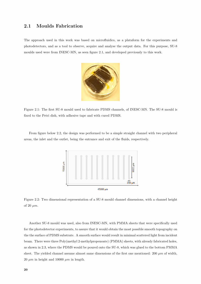
photodetectors, and as a tool to observe, acquire and analyse the output data. For this purpose, SU-8
moulds used were from INESC-MN, as seen figure 2.1, and developed previously to this work.
Figure 2.1: The first SU-8 mould used to fabricate PDMS channels, of INESC-MN. The SU-8 mould is
fixed to the Petri dish, with adhesive tape and with cured PDMS.
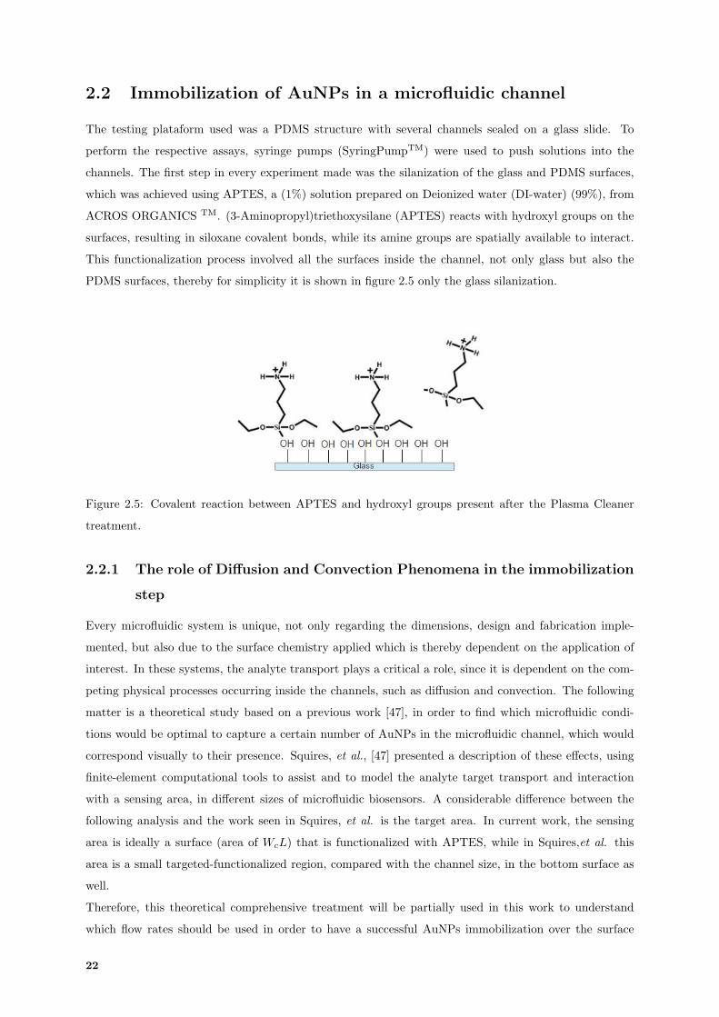
From figure below 2.2, the design was performed to be a simple straight channel with two peripheral
areas, the inlet and the outlet, being the entrance and exit of the fluids, respectively.
Figure 2.2: Two dimensional representation of a SU-8 mould channel dimensions, with a channel height
of 20 µm.
Another SU-8 mould was used, also from INESC-MN, with PMMA sheets that were specifically used
for the photodetector experiments, to assure that it would obtain the most possible smooth topography on
the the surface of PDMS substrate. A smooth surface would result in minimal scattered light from incident
beam. There were three Poly(methyl 2-methylpropenoate) (PMMA) sheets, with already fabricated holes,
as shown in 2.3, where the PDMS would be poured onto the SU-8, which was glued to the bottom PMMA
sheet. The yielded channel assume almost same dimensions of the first one mentioned: 200 µm of width,
20 µm in height and 10000 µm in length.
20

Figure 2.3: PMMA sheets that held the SU-mould in order to produce PDMS microfluidic channels.
In order to obtain several channels as a platform for the experiments, PDMS was prepared using
the base (SYLGARD 184 silicone elastomer by DOW CORNING) and a curing agent (SYLGARD 184
silicone elastomer by DOW CORNING) using a ratio 10:1 (w:w), respectively. After stirring both in
a plastic cup, it was degassed in a vacuum chamber for 1 hour and 30 min, so that air bubbles were
removed. This mixture was poured on top of each SU-8 mould and put in Memmert oven, at 70 C to be
baked for 1 hour and 15 min, showed schematically shown in figure 2.4. The PDMS structure was cut
and separated from the mould, then it was necessary to punch holes in the outlet and inlet spots to allow
the entrance of adapters and tubes, using a syring needle tip.
Figure 2.4: PDMS Microchannel fabrication scheme, with fundamental steps (not at real scale).
2.1.1 Surface Functionalization of PDMS Microchannels
The PDMS prepared was sealed on thin glass, Menzel-GlaserTM, 50× 24 mm. Each glass was washed in
Alconox for 30 min, then washed with acetone, isopropyl alcohol and water, finishing with N2 blow-dry
gun. The first surface derivatization process was performed with UV-O treatment (UVO cleaner 144AX,
Jelight Company Inc.TM), where a UV lamp would create reactive hydroxyl groups at the surfaces during
11 min (6 min to clean and 5 min to exhaust). Since, during this project, INESC-MN acquired the
Plasma equipment, all the following described experiments were initialized by using this prefered sealing
process. PDMS and glass surfaces were put in Plasma Cleaner (Harrick PlasmaTM), where an Oxygen
plasma would activate these surfaces for 1 min, creating reactive OH negative groups. Then, PDMS and
glass were assembled together, gently and manually pressed to seal together, and put over a hotplate at
130 C for 5 min.
21
2.2 Immobilization of AuNPs in a microfluidic channel
The testing plataform used was a PDMS structure with several channels sealed on a glass slide. To
perform the respective assays, syringe pumps (SyringPumpTM) were used to push solutions into the
channels. The first step in every experiment made was the silanization of the glass and PDMS surfaces,
which was achieved using APTES, a (1%) solution prepared on Deionized water (DI-water) (99%), from
ACROS ORGANICS TM. (3-Aminopropyl)triethoxysilane (APTES) reacts with hydroxyl groups on the
surfaces, resulting in siloxane covalent bonds, while its amine groups are spatially available to interact.
This functionalization process involved all the surfaces inside the channel, not only glass but also the
PDMS surfaces, thereby for simplicity it is shown in figure 2.5 only the glass silanization.
Figure 2.5: Covalent reaction between APTES and hydroxyl groups present after the Plasma Cleaner
treatment.
2.2.1 The role of Diffusion and Convection Phenomena in the immobilization
step
Every microfluidic system is unique, not only regarding the dimensions, design and fabrication imple-
mented, but also due to the surface chemistry applied which is thereby dependent on the application of
interest. In these systems, the analyte transport plays a critical a role, since it is dependent on the com-
peting physical processes occurring inside the channels, such as diffusion and convection. The following
matter is a theoretical study based on a previous work [47], in order to find which microfluidic condi-
tions would be optimal to capture a certain number of AuNPs in the microfluidic channel, which would
correspond visually to their presence. Squires, et al., [47] presented a description of these effects, using
finite-element computational tools to assist and to model the analyte target transport and interaction
with a sensing area, in different sizes of microfluidic biosensors. A considerable difference between the
following analysis and the work seen in Squires, et al. is the target area. In current work, the sensing
area is ideally a surface (area of WcL) that is functionalized with APTES, while in Squires,et al. this
area is a small targeted-functionalized region, compared with the channel size, in the bottom surface as
well.
Therefore, this theoretical comprehensive treatment will be partially used in this work to understand
which flow rates should be used in order to have a successful AuNPs immobilization over the surface
22
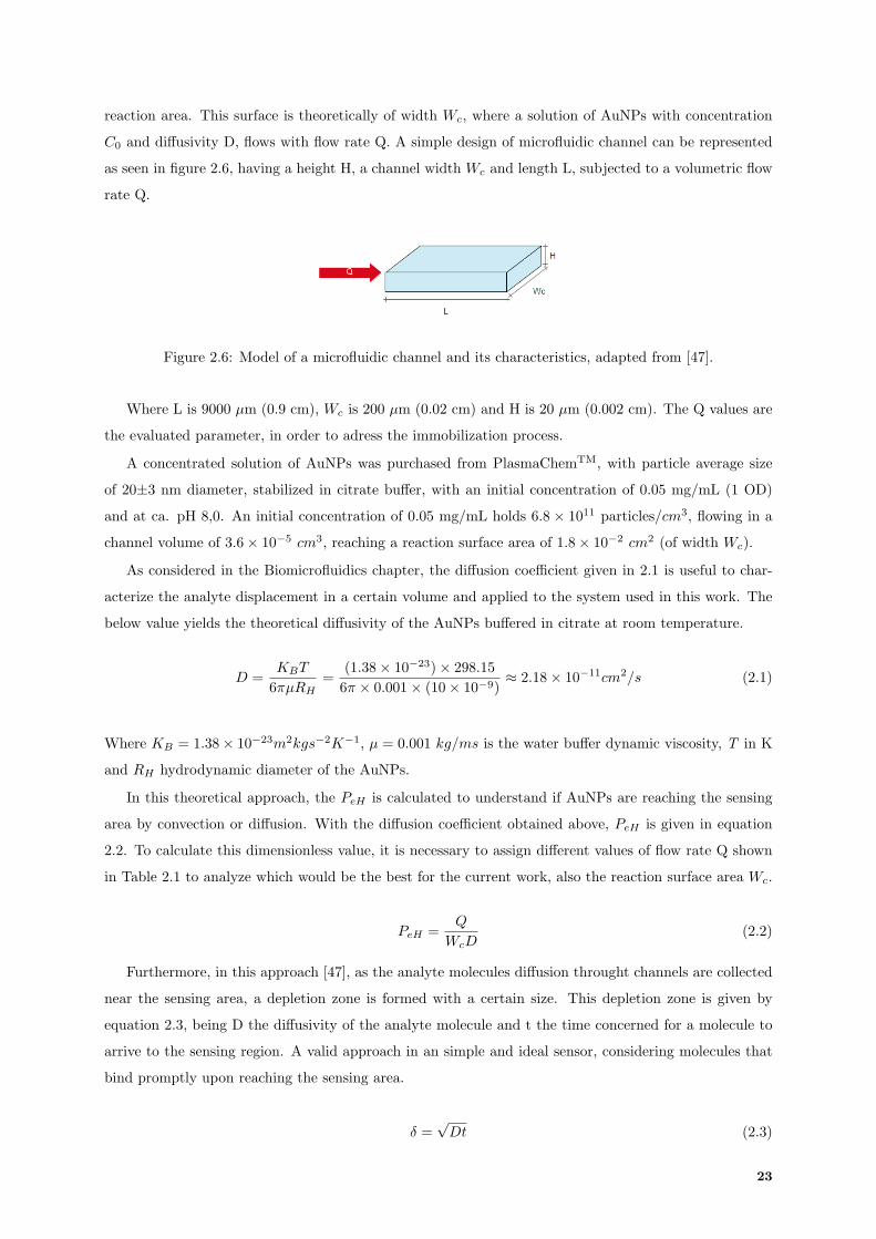
reaction area. This surface is theoretically of width Wc, where a solution of AuNPs with concentration
C0 and diffusivity D, flows with flow rate Q. A simple design of microfluidic channel can be represented
as seen in figure 2.6, having a height H, a channel width Wc and length L, subjected to a volumetric flow
rate Q.
Figure 2.6: Model of a microfluidic channel and its characteristics, adapted from [47].
Where L is 9000 µm (0.9 cm), Wc is 200 µm (0.02 cm) and H is 20 µm (0.002 cm). The Q values are
the evaluated parameter, in order to adress the immobilization process.
A concentrated solution of AuNPs was purchased from PlasmaChemTM, with particle average size
of 20±3 nm diameter, stabilized in citrate buffer, with an initial concentration of 0.05 mg/mL (1 OD)
and at ca. pH 8,0. An initial concentration of 0.05 mg/mL holds 6.8 × 10¹¹ particles/cm3, flowing in a
channel volume of 3.6× 10⁻⁵ cm3, reaching a reaction surface area of 1.8× 10⁻² cm2 (of width Wc).
As considered in the Biomicrofluidics chapter, the diffusion coefficient given in 2.1 is useful to char-
acterize the analyte displacement in a certain volume and applied to the system used in this work. The
below value yields the theoretical diffusivity of the AuNPs buffered in citrate at room temperature.
D =KBT
6πµRH=
(1.38× 10−23)× 298.15
6π × 0.001× (10× 10−9)≈ 2.18× 10⁻¹¹cm2/s (2.1)
Where KB = 1.38× 10⁻²³m2kgs−2K−1, µ = 0.001 kg/ms is the water buffer dynamic viscosity, T in K
and RH hydrodynamic diameter of the AuNPs.
In this theoretical approach, the PeH is calculated to understand if AuNPs are reaching the sensing
area by convection or diffusion. With the diffusion coefficient obtained above, PeH is given in equation
2.2. To calculate this dimensionless value, it is necessary to assign different values of flow rate Q shown
in Table 2.1 to analyze which would be the best for the current work, also the reaction surface area Wc.
PeH =Q
WcD(2.2)
Furthermore, in this approach [47], as the analyte molecules diffusion throught channels are collected
near the sensing area, a depletion zone is formed with a certain size. This depletion zone is given by
equation 2.3, being D the diffusivity of the analyte molecule and t the time concerned for a molecule to
arrive to the sensing region. A valid approach in an simple and ideal sensor, considering molecules that
bind promptly upon reaching the sensing area.
δ =√Dt (2.3)
23
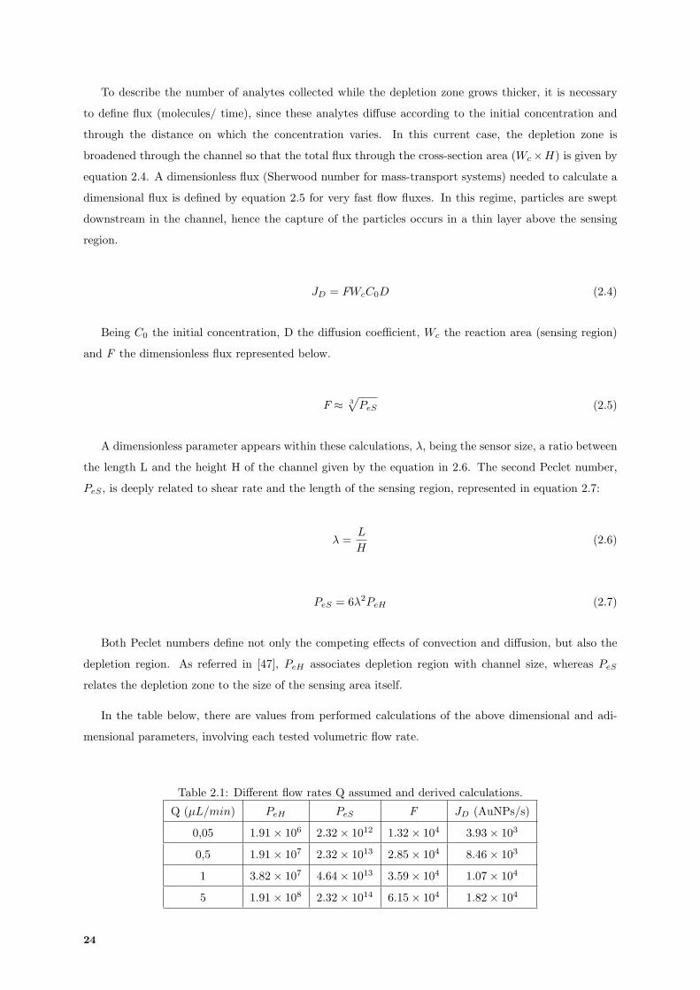
To describe the number of analytes collected while the depletion zone grows thicker, it is necessary
to define flux (molecules/ time), since these analytes diffuse according to the initial concentration and
through the distance on which the concentration varies. In this current case, the depletion zone is
broadened through the channel so that the total flux through the cross-section area (Wc×H) is given by
equation 2.4. A dimensionless flux (Sherwood number for mass-transport systems) needed to calculate a
dimensional flux is defined by equation 2.5 for very fast flow fluxes. In this regime, particles are swept
downstream in the channel, hence the capture of the particles occurs in a thin layer above the sensing
region.
JD = FWcC0D (2.4)
Being C0 the initial concentration, D the diffusion coefficient, Wc the reaction area (sensing region)
and F the dimensionless flux represented below.
F ≈ 3√PeS (2.5)
A dimensionless parameter appears within these calculations, λ, being the sensor size, a ratio between
the length L and the height H of the channel given by the equation in 2.6. The second Peclet number,
PeS , is deeply related to shear rate and the length of the sensing region, represented in equation 2.7:
λ =L
H(2.6)
PeS = 6λ2PeH (2.7)
Both Peclet numbers define not only the competing effects of convection and diffusion, but also the
depletion region. As referred in [47], PeH associates depletion region with channel size, whereas PeS
relates the depletion zone to the size of the sensing area itself.
In the table below, there are values from performed calculations of the above dimensional and adi-
mensional parameters, involving each tested volumetric flow rate.
Table 2.1: Different flow rates Q assumed and derived calculations.
Q (µL/min) PeH PeS F JD (AuNPs/s)
0,05 1.91× 10⁶ 2.32× 10¹² 1.32× 10⁴ 3.93× 10³
0,5 1.91× 10⁷ 2.32× 10¹³ 2.85× 10⁴ 8.46× 10³
1 3.82× 10⁷ 4.64× 10¹³ 3.59× 10⁴ 1.07× 10⁴
5 1.91× 10⁸ 2.32× 10¹⁴ 6.15× 10⁴ 1.82× 10⁴
24
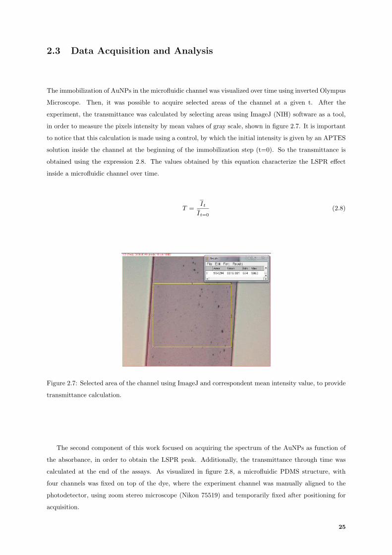
2.3 Data Acquisition and Analysis
The immobilization of AuNPs in the microfluidic channel was visualized over time using inverted Olympus
Microscope. Then, it was possible to acquire selected areas of the channel at a given t. After the
experiment, the transmittance was calculated by selecting areas using ImageJ (NIH) software as a tool,
in order to measure the pixels intensity by mean values of gray scale, shown in figure 2.7. It is important
to notice that this calculation is made using a control, by which the initial intensity is given by an APTES
solution inside the channel at the beginning of the immobilization step (t=0). So the transmittance is
obtained using the expression 2.8. The values obtained by this equation characterize the LSPR effect
inside a microfluidic channel over time.
T =It
It=0
(2.8)
Figure 2.7: Selected area of the channel using ImageJ and correspondent mean intensity value, to provide
transmittance calculation.
The second component of this work focused on acquiring the spectrum of the AuNPs as function of
the absorbance, in order to obtain the LSPR peak. Additionally, the transmittance through time was
calculated at the end of the assays. As visualized in figure 2.8, a microfluidic PDMS structure, with
four channels was fixed on top of the dye, where the experiment channel was manually aligned to the
photodetector, using zoom stereo microscope (Nikon 75519) and temporarily fixed after positioning for
acquisition.
25
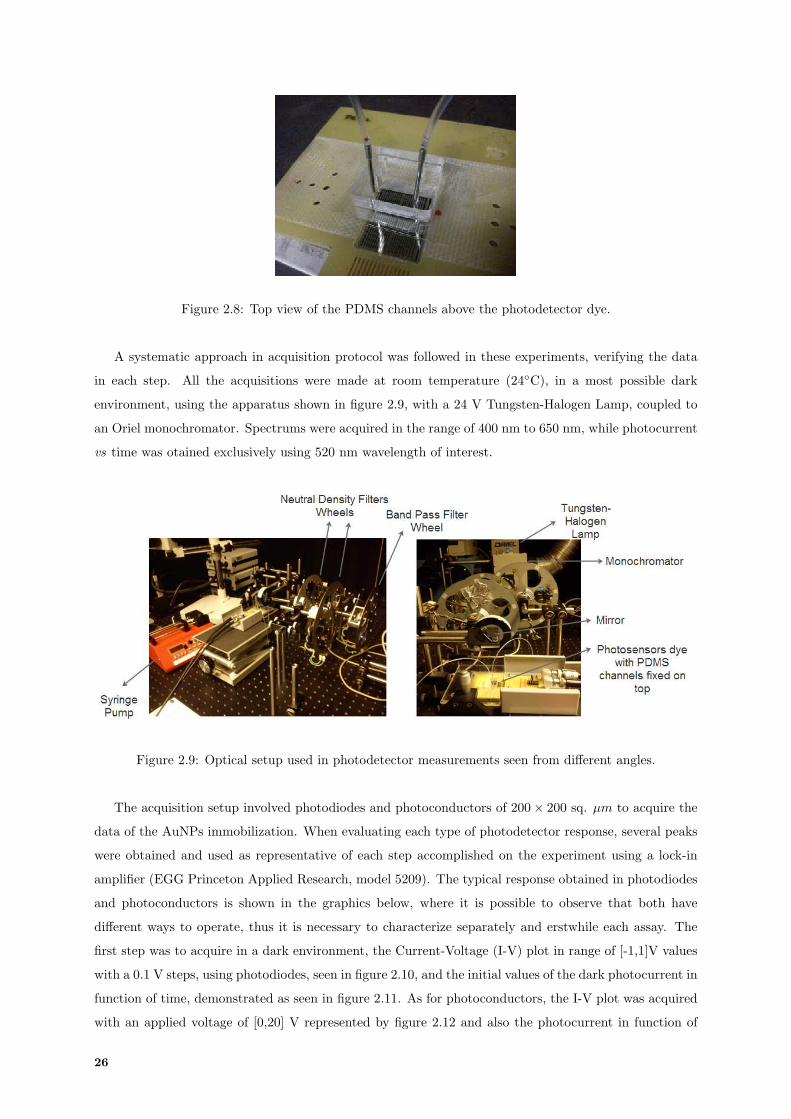
Figure 2.8: Top view of the PDMS channels above the photodetector dye.
A systematic approach in acquisition protocol was followed in these experiments, verifying the data
in each step. All the acquisitions were made at room temperature (24C), in a most possible dark
environment, using the apparatus shown in figure 2.9, with a 24 V Tungsten-Halogen Lamp, coupled to
an Oriel monochromator. Spectrums were acquired in the range of 400 nm to 650 nm, while photocurrent
vs time was otained exclusively using 520 nm wavelength of interest.
Figure 2.9: Optical setup used in photodetector measurements seen from different angles.
The acquisition setup involved photodiodes and photoconductors of 200× 200 sq. µm to acquire the
data of the AuNPs immobilization. When evaluating each type of photodetector response, several peaks
were obtained and used as representative of each step accomplished on the experiment using a lock-in
amplifier (EGG Princeton Applied Research, model 5209). The typical response obtained in photodiodes
and photoconductors is shown in the graphics below, where it is possible to observe that both have
different ways to operate, thus it is necessary to characterize separately and erstwhile each assay. The
first step was to acquire in a dark environment, the Current-Voltage (I-V) plot in range of [-1,1]V values
with a 0.1 V steps, using photodiodes, seen in figure 2.10, and the initial values of the dark photocurrent in
function of time, demonstrated as seen in figure 2.11. As for photoconductors, the I-V plot was acquired
with an applied voltage of [0,20] V represented by figure 2.12 and also the photocurrent in function of
26
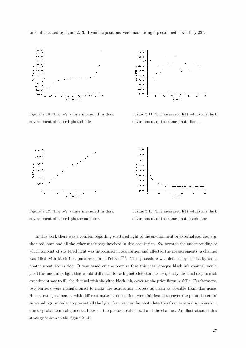
time, illustrated by figure 2.13. Twain acquisitions were made using a picoammeter Keithley 237.
Figure 2.10: The I-V values measured in dark
environment of a used photodiode.
Figure 2.11: The measured I(t) values in a dark
environment of the same photodiode.
Figure 2.12: The I-V values measured in dark
environment of a used photoconductor.
Figure 2.13: The measured I(t) values in a dark
environment of the same photoconductor.
In this work there was a concern regarding scattered light of the environment or external sources, e.g.
the used lamp and all the other machinery involved in this acquisition. So, towards the understanding of
which amount of scattered light was introduced in acquisition and affected the measurements, a channel
was filled with black ink, purchased from PelikanTM. This procedure was defined by the background
photocurrent acquisition. It was based on the premise that this ideal opaque black ink channel would
yield the amount of light that would still reach to each photodetector. Consequently, the final step in each
experiment was to fill the channel with the cited black ink, covering the prior flown AuNPs. Furthermore,
two barriers were manufactured to make the acquisition process as clean as possible from this noise.
Hence, two glass masks, with different material deposition, were fabricated to cover the photodetectors’
surroundings, in order to prevent all the light that reaches the photodetectors from external sourcers and
due to probable misalignments, between the photodetector itself and the channel. An illustration of this
strategy is seen in the figure 2.14:
27
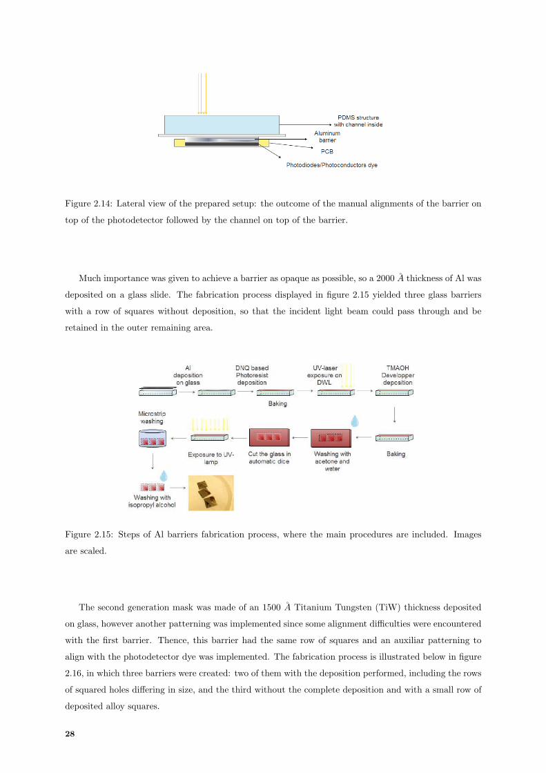
Figure 2.14: Lateral view of the prepared setup: the outcome of the manual alignments of the barrier on
top of the photodetector followed by the channel on top of the barrier.
Much importance was given to achieve a barrier as opaque as possible, so a 2000 A thickness of Al was
deposited on a glass slide. The fabrication process displayed in figure 2.15 yielded three glass barriers
with a row of squares without deposition, so that the incident light beam could pass through and be
retained in the outer remaining area.
Figure 2.15: Steps of Al barriers fabrication process, where the main procedures are included. Images
are scaled.
The second generation mask was made of an 1500 A Titanium Tungsten (TiW) thickness deposited
on glass, however another patterning was implemented since some alignment difficulties were encountered
with the first barrier. Thence, this barrier had the same row of squares and an auxiliar patterning to
align with the photodetector dye was implemented. The fabrication process is illustrated below in figure
2.16, in which three barriers were created: two of them with the deposition performed, including the rows
of squared holes differing in size, and the third without the complete deposition and with a small row of
deposited alloy squares.
28
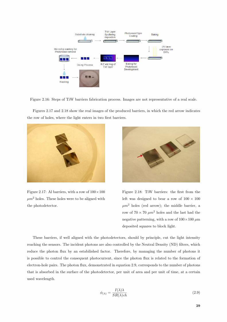
Figure 2.16: Steps of TiW barriers fabrication process. Images are not representative of a real scale.
Figures 2.17 and 2.18 show the real images of the produced barriers, in which the red arrow indicates
the row of holes, where the light enters in two first barriers.
Figure 2.17: Al barriers, with a row of 100×100
µm2 holes. These holes were to be aligned with
the photodetector.
Figure 2.18: TiW barriers: the first from the
left was designed to bear a row of 100 × 100
µm2 holes (red arrow); the middle barrier, a
row of 70 × 70 µm2 holes and the last had the
negative patterning, with a row of 100×100 µm
deposited squares to block light.
These barriers, if well aligned with the photodetectors, should by principle, cut the light intensity
reaching the sensors. The incident photons are also controlled by the Neutral Density (ND) filters, which
reduce the photon flux by an estabilished factor. Therefore, by managing the number of photons it
is possible to control the consequent photocurrent, since the photon flux is related to the formation of
electron-hole pairs. The photon flux, demonstrated in equation 2.9, corresponds to the number of photons
that is absorbed in the surface of the photodetector, per unit of area and per unit of time, at a certain
used wavelength.
φ(λ) =I(λ)λ
SR(λ)ch(2.9)
29
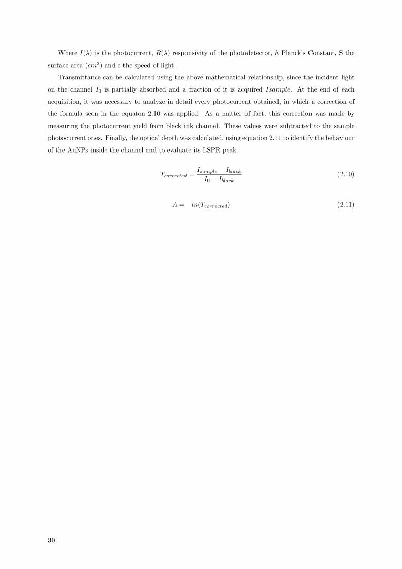
Where I(λ) is the photocurrent, R(λ) responsivity of the photodetector, h Planck’s Constant, S the
surface area (cm2) and c the speed of light.
Transmittance can be calculated using the above mathematical relationship, since the incident light
on the channel I0 is partially absorbed and a fraction of it is acquired Isample. At the end of each
acquisition, it was necessary to analyze in detail every photocurrent obtained, in which a correction of
the formula seen in the equaton 2.10 was applied. As a matter of fact, this correction was made by
measuring the photocurrent yield from black ink channel. These values were subtracted to the sample
photocurrent ones. Finally, the optical depth was calculated, using equation 2.11 to identify the behaviour
of the AuNPs inside the channel and to evaluate its LSPR peak.
Tcorrected =Isample − IblackI0 − Iblack
(2.10)
A = −ln(Tcorrected) (2.11)
30

3Results and Discussion
Contents
3.1 Gold Nanoparticles: making their way into channels . . . . . . . . . . . . . 32
3.2 Scanning Electron Microscopy as a tool for insight . . . . . . . . . . . . . . 40
3.3 Localized Surface Plasmon Resonance Detection . . . . . . . . . . . . . . . 47
31
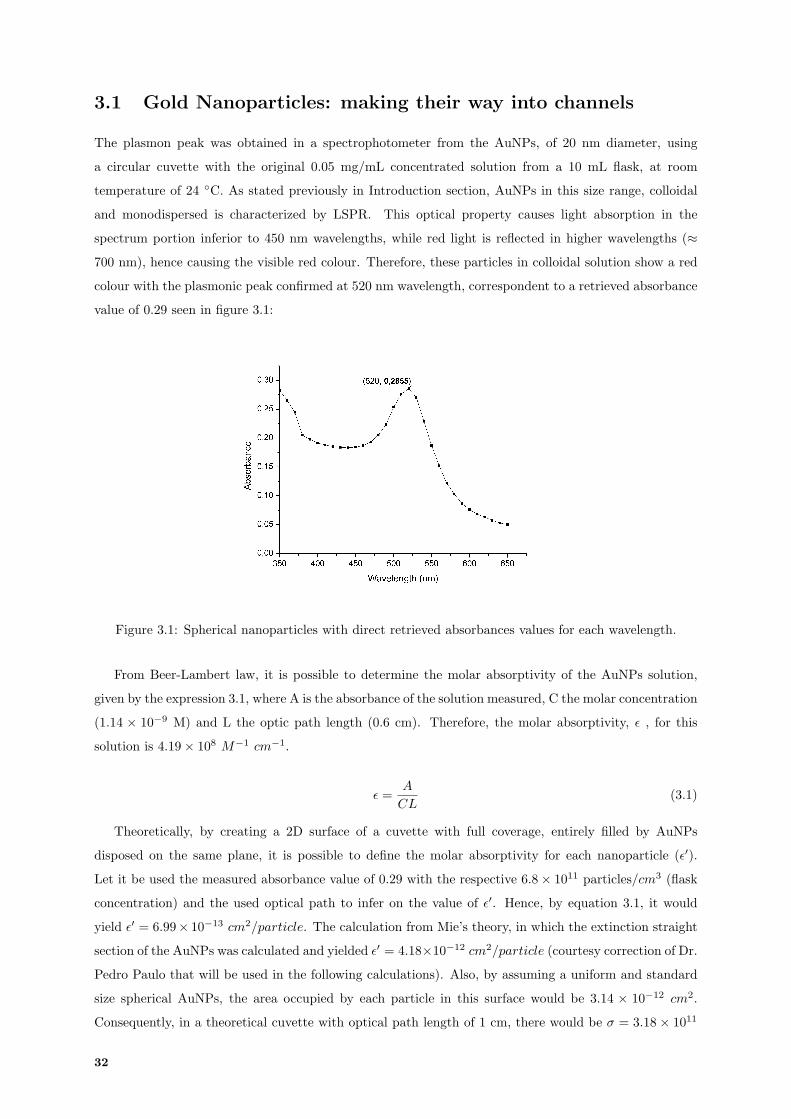
3.1 Gold Nanoparticles: making their way into channels
The plasmon peak was obtained in a spectrophotometer from the AuNPs, of 20 nm diameter, using
a circular cuvette with the original 0.05 mg/mL concentrated solution from a 10 mL flask, at room
temperature of 24 C. As stated previously in Introduction section, AuNPs in this size range, colloidal
and monodispersed is characterized by LSPR. This optical property causes light absorption in the
spectrum portion inferior to 450 nm wavelengths, while red light is reflected in higher wavelengths (≈
700 nm), hence causing the visible red colour. Therefore, these particles in colloidal solution show a red
colour with the plasmonic peak confirmed at 520 nm wavelength, correspondent to a retrieved absorbance
value of 0.29 seen in figure 3.1:
Figure 3.1: Spherical nanoparticles with direct retrieved absorbances values for each wavelength.
From Beer-Lambert law, it is possible to determine the molar absorptivity of the AuNPs solution,
given by the expression 3.1, where A is the absorbance of the solution measured, C the molar concentration
(1.14 × 10⁻⁹ M) and L the optic path length (0.6 cm). Therefore, the molar absorptivity, ε , for this
solution is 4.19× 10⁸ M−1 cm−1.
ε =A
CL(3.1)
Theoretically, by creating a 2D surface of a cuvette with full coverage, entirely filled by AuNPs
disposed on the same plane, it is possible to define the molar absorptivity for each nanoparticle (ε′).
Let it be used the measured absorbance value of 0.29 with the respective 6.8× 10¹¹ particles/cm3 (flask
concentration) and the used optical path to infer on the value of ε′. Hence, by equation 3.1, it would
yield ε′ = 6.99× 10⁻¹³ cm2/particle. The calculation from Mie’s theory, in which the extinction straight
section of the AuNPs was calculated and yielded ε′ = 4.18×10⁻¹² cm2/particle (courtesy correction of Dr.
Pedro Paulo that will be used in the following calculations). Also, by assuming a uniform and standard
size spherical AuNPs, the area occupied by each particle in this surface would be 3.14 × 10⁻¹² cm2.
Consequently, in a theoretical cuvette with optical path length of 1 cm, there would be σ = 3.18× 10¹¹
32
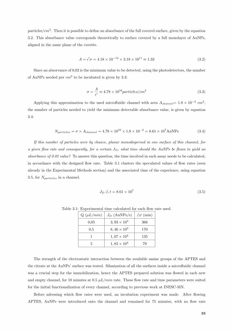
particles/cm2. Then it is possible to define an absorbance of the full covered surface, given by the equation
3.2. This absorbance value corresponds theoretically to surface covered by a full monolayer of AuNPs,
aligned in the same plane of the cuvette.
A = ε′σ = 4.18× 10−12 × 3.18× 1011 ≈ 1.33 (3.2)
Since an absorvance of 0,02 is the minimum value to be detected, using the photodetectors, the number
of AuNPs needed per cm2 to be incubated is given by 3.3:
σ =A
ε′≈ 4.78× 10¹⁰particles/cm2 (3.3)
Applying this approximation to the used microfluidic channel with area Achannel= 1.8 × 10⁻² cm2,
the number of particles needed to yield the minimum detectable absorbance value, is given by equation
3.4:
Nparticles = σ ×Achannel = 4.78× 1010 × 1.8× 10−2 = 8.61× 10⁷AuNPs (3.4)
If this number of particles were by chance, planar monodispersed in one surface of this channel, for
a given flow rate and consequently, for a certain JD, what time should the AuNPs be flown to yield an
absorbance of 0.02 value? To answer this question, the time involved in each assay needs to be calculated,
in accordance with the designed flow rate. Table 3.1 clusters the speculated values of flow rates (seen
already in the Experimental Methods section) and the associated time of the experience, using equation
3.5, for Nparticles in a channel.
JD 4 t = 8.61× 10⁷ (3.5)
Table 3.1: Experimental time calculated for each flow rate used.
Q (µL/min) JD (AuNPs/s) 4t (min)
0,05 3, 93× 103 366
0,5 8, 46× 103 170
1 1, 07× 104 135
5 1, 82× 104 79
The strength of the electrostatic interaction between the available amine groups of the APTES and
the citrate at the AuNPs’ surface was tested. Silanization of all the surfaces inside a microfluidic channel
was a crucial step for the immobilization, hence the APTES prepared solution was flowed in each new
and empty channel, for 10 minutes at 0.5 µL/min rate. These flow rate and time parameters were suited
for the initial functionalization of every channel, according to previous work at INESC-MN.
Before adressing which flow rates were used, an incubation experiment was made. After flowing
APTES, AuNPs were introduced onto the channel and remained for 75 minutes, with no flow rate
33
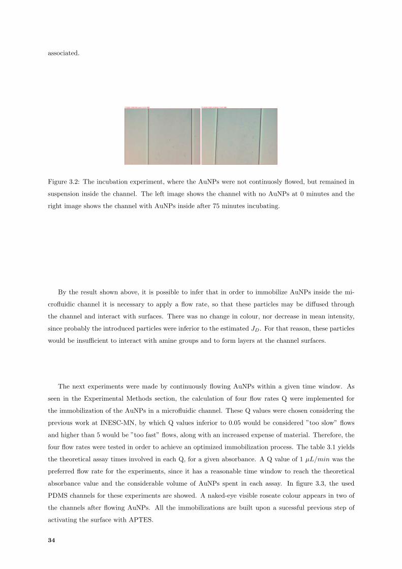
associated.
Figure 3.2: The incubation experiment, where the AuNPs were not continuosly flowed, but remained in
suspension inside the channel. The left image shows the channel with no AuNPs at 0 minutes and the
right image shows the channel with AuNPs inside after 75 minutes incubating.
By the result shown above, it is possible to infer that in order to immobilize AuNPs inside the mi-
crofluidic channel it is necessary to apply a flow rate, so that these particles may be diffused through
the channel and interact with surfaces. There was no change in colour, nor decrease in mean intensity,
since probably the introduced particles were inferior to the estimated JD. For that reason, these particles
would be insufficient to interact with amine groups and to form layers at the channel surfaces.
The next experiments were made by continuously flowing AuNPs within a given time window. As
seen in the Experimental Methods section, the calculation of four flow rates Q were implemented for
the immobilization of the AuNPs in a microfluidic channel. These Q values were chosen considering the
previous work at INESC-MN, by which Q values inferior to 0.05 would be considered ”too slow” flows
and higher than 5 would be ”too fast” flows, along with an increased expense of material. Therefore, the
four flow rates were tested in order to achieve an optimized immobilization process. The table 3.1 yields
the theoretical assay times involved in each Q, for a given absorbance. A Q value of 1 µL/min was the
preferred flow rate for the experiments, since it has a reasonable time window to reach the theoretical
absorbance value and the considerable volume of AuNPs spent in each assay. In figure 3.3, the used
PDMS channels for these experiments are showed. A naked-eye visible roseate colour appears in two of
the channels after flowing AuNPs. All the immobilizations are built upon a sucessful previous step of
activating the surface with APTES.
34
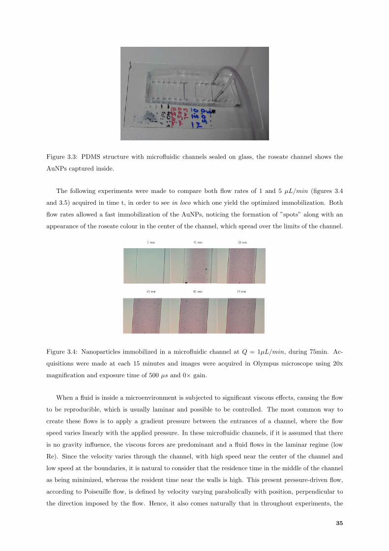
Figure 3.3: PDMS structure with microfluidic channels sealed on glass, the roseate channel shows the
AuNPs captured inside.
The following experiments were made to compare both flow rates of 1 and 5 µL/min (figures 3.4
and 3.5) acquired in time t, in order to see in loco which one yield the optimized immobilization. Both
flow rates allowed a fast immobilization of the AuNPs, noticing the formation of ”spots” along with an
appearance of the roseate colour in the center of the channel, which spread over the limits of the channel.
Figure 3.4: Nanoparticles immobilized in a microfluidic channel at Q = 1µL/min, during 75min. Ac-
quisitions were made at each 15 minutes and images were acquired in Olympus microscope using 20x
magnification and exposure time of 500 µs and 0× gain.
When a fluid is inside a microenvironment is subjected to significant viscous effects, causing the flow
to be reproducible, which is usually laminar and possible to be controlled. The most common way to
create these flows is to apply a gradient pressure between the entrances of a channel, where the flow
speed varies linearly with the applied pressure. In these microfluidic channels, if it is assumed that there
is no gravity influence, the viscous forces are predominant and a fluid flows in the laminar regime (low
Re). Since the velocity varies through the channel, with high speed near the center of the channel and
low speed at the boundaries, it is natural to consider that the residence time in the middle of the channel
as being minimized, whereas the resident time near the walls is high. This present pressure-driven flow,
according to Poiseuille flow, is defined by velocity varying parabolically with position, perpendicular to
the direction imposed by the flow. Hence, it also comes naturally that in throughout experiments, the
35
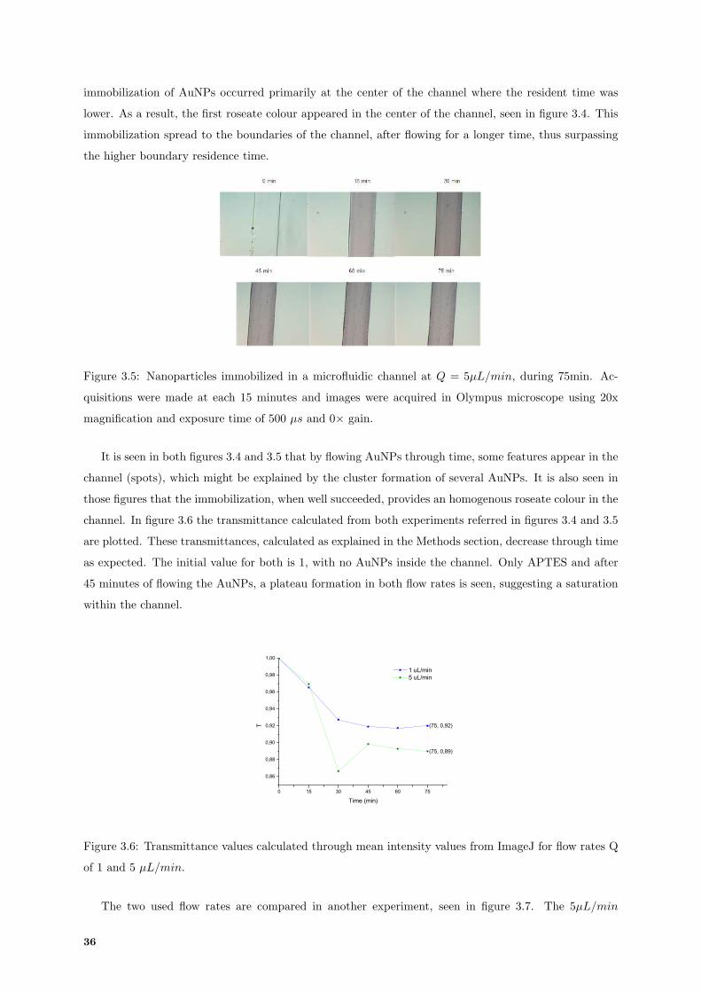
immobilization of AuNPs occurred primarily at the center of the channel where the resident time was
lower. As a result, the first roseate colour appeared in the center of the channel, seen in figure 3.4. This
immobilization spread to the boundaries of the channel, after flowing for a longer time, thus surpassing
the higher boundary residence time.
Figure 3.5: Nanoparticles immobilized in a microfluidic channel at Q = 5µL/min, during 75min. Ac-
quisitions were made at each 15 minutes and images were acquired in Olympus microscope using 20x
magnification and exposure time of 500 µs and 0× gain.
It is seen in both figures 3.4 and 3.5 that by flowing AuNPs through time, some features appear in the
channel (spots), which might be explained by the cluster formation of several AuNPs. It is also seen in
those figures that the immobilization, when well succeeded, provides an homogenous roseate colour in the
channel. In figure 3.6 the transmittance calculated from both experiments referred in figures 3.4 and 3.5
are plotted. These transmittances, calculated as explained in the Methods section, decrease through time
as expected. The initial value for both is 1, with no AuNPs inside the channel. Only APTES and after
45 minutes of flowing the AuNPs, a plateau formation in both flow rates is seen, suggesting a saturation
within the channel.
0 15 30 45 60 75
0,86
0,88
0,90
0,92
0,94
0,96
0,98
1,00
1 uL/min 5 uL/min
T
Time (min)
(75, 0,92)
(75, 0,89)
Figure 3.6: Transmittance values calculated through mean intensity values from ImageJ for flow rates Q
of 1 and 5 µL/min.
The two used flow rates are compared in another experiment, seen in figure 3.7. The 5µL/min
36
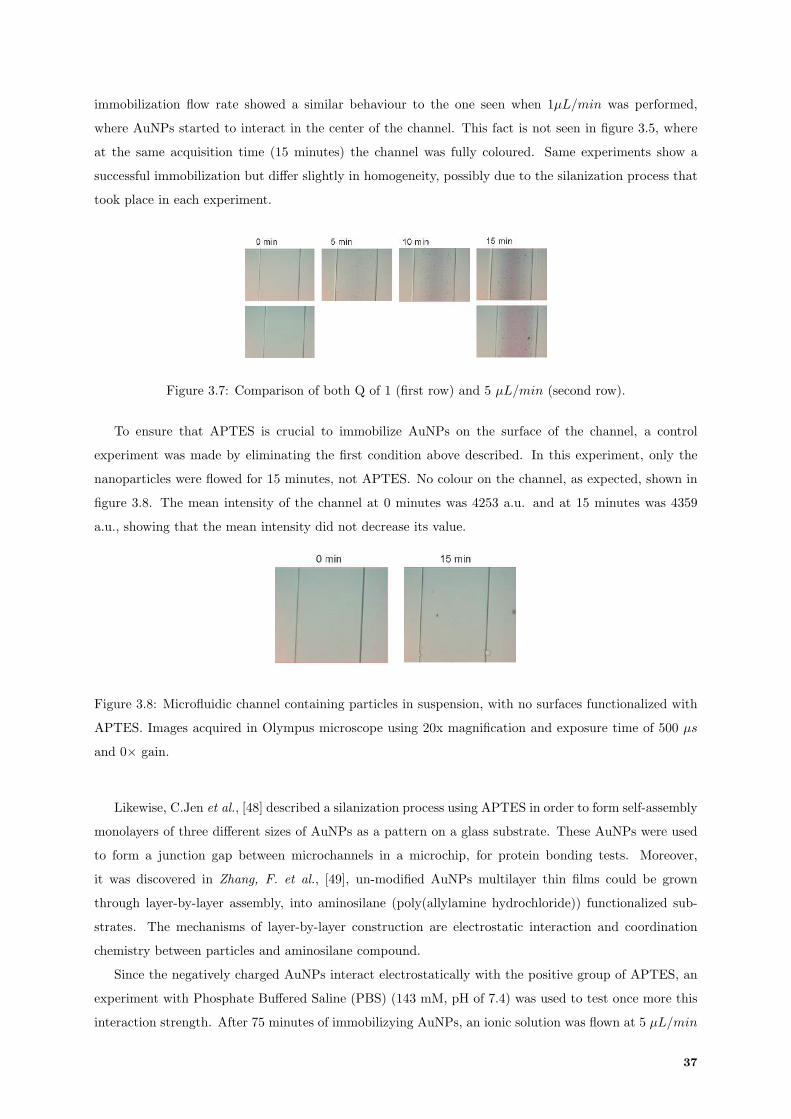
immobilization flow rate showed a similar behaviour to the one seen when 1µL/min was performed,
where AuNPs started to interact in the center of the channel. This fact is not seen in figure 3.5, where
at the same acquisition time (15 minutes) the channel was fully coloured. Same experiments show a
successful immobilization but differ slightly in homogeneity, possibly due to the silanization process that
took place in each experiment.
Figure 3.7: Comparison of both Q of 1 (first row) and 5 µL/min (second row).
To ensure that APTES is crucial to immobilize AuNPs on the surface of the channel, a control
experiment was made by eliminating the first condition above described. In this experiment, only the
nanoparticles were flowed for 15 minutes, not APTES. No colour on the channel, as expected, shown in
figure 3.8. The mean intensity of the channel at 0 minutes was 4253 a.u. and at 15 minutes was 4359
a.u., showing that the mean intensity did not decrease its value.
Figure 3.8: Microfluidic channel containing particles in suspension, with no surfaces functionalized with
APTES. Images acquired in Olympus microscope using 20x magnification and exposure time of 500 µs
and 0× gain.
Likewise, C.Jen et al., [48] described a silanization process using APTES in order to form self-assembly
monolayers of three different sizes of AuNPs as a pattern on a glass substrate. These AuNPs were used
to form a junction gap between microchannels in a microchip, for protein bonding tests. Moreover,
it was discovered in Zhang, F. et al., [49], un-modified AuNPs multilayer thin films could be grown
through layer-by-layer assembly, into aminosilane (poly(allylamine hydrochloride)) functionalized sub-
strates. The mechanisms of layer-by-layer construction are electrostatic interaction and coordination
chemistry between particles and aminosilane compound.
Since the negatively charged AuNPs interact electrostatically with the positive group of APTES, an
experiment with Phosphate Buffered Saline (PBS) (143 mM, pH of 7.4) was used to test once more this
interaction strength. After 75 minutes of immobilizying AuNPs, an ionic solution was flown at 5 µL/min
37
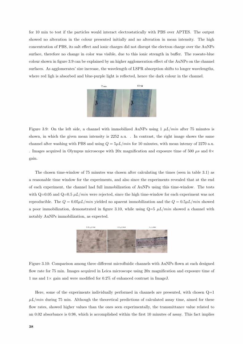
for 10 min to test if the particles would interact electrostatically with PBS over APTES. The output
showed no alteration in the colour presented initially and no alteration in mean intensity. The high
concentration of PBS, its salt effect and ionic charges did not disrupt the electron charge over the AuNPs
surface, therefore no change in color was visible, due to this ionic strength in buffer. The roseate-blue
colour shown in figure 3.9 can be explained by an higher agglomeration effect of the AuNPs on the channel
surfaces. As agglomerates’ size increase, the wavelength of LSPR absorption shifts to longer wavelengths,
where red ligh is absorbed and blue-purple light is reflected, hence the dark colour in the channel.
Figure 3.9: On the left side, a channel with immobilized AuNPs using 1 µL/min after 75 minutes is
shown, in which the given mean intensity is 2252 a.u. . In contrast, the right image shows the same
channel after washing with PBS and using Q = 5µL/min for 10 minutes, with mean intensy of 2270 a.u.
. Images acquired in Olympus microscope with 20x magnification and exposure time of 500 µs and 0×
gain.
The chosen time-window of 75 minutes was chosen after calculating the times (seen in table 3.1) as
a reasonable time window for the experiments, and also since the experiments revealed that at the end
of each experiment, the channel had full immobilization of AuNPs using this time-window. The tests
with Q=0.05 and Q=0.5 µL/min were rejected, since the high time-window for each experiment was not
reproducible. The Q = 0.05µL/min yielded no aparent immobilization and the Q = 0.5µL/min showed
a poor immobilization, demonstrated in figure 3.10, while using Q=5 µL/min showed a channel with
notably AuNPs immobilization, as expected.
Figure 3.10: Comparison among three different microfluidic channels with AuNPs flown at each designed
flow rate for 75 min. Images acquired in Leica microscope using 20x magnification and exposure time of
1 ms and 1× gain and were modified for 0.2% of enhanced contrast in ImageJ.
Here, some of the experiments individually performed in channels are presented, with chosen Q=1
µL/min during 75 min. Although the theoretical predictions of calculated assay time, aimed for these
flow rates, showed higher values than the ones seen experimentally, the transmittance value related to
an 0.02 absorbance is 0.98, which is accomplished within the first 10 minutes of assay. This fact implies
38
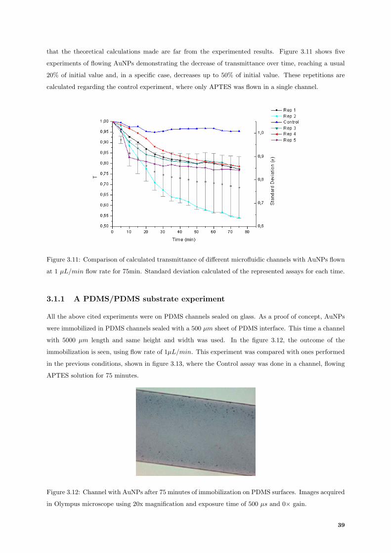
that the theoretical calculations made are far from the experimented results. Figure 3.11 shows five
experiments of flowing AuNPs demonstrating the decrease of transmittance over time, reaching a usual
20% of initial value and, in a specific case, decreases up to 50% of initial value. These repetitions are
calculated regarding the control experiment, where only APTES was flown in a single channel.
Figure 3.11: Comparison of calculated transmittance of different microfluidic channels with AuNPs flown
at 1 µL/min flow rate for 75min. Standard deviation calculated of the represented assays for each time.
3.1.1 A PDMS/PDMS substrate experiment
All the above cited experiments were on PDMS channels sealed on glass. As a proof of concept, AuNPs
were immobilized in PDMS channels sealed with a 500 µm sheet of PDMS interface. This time a channel
with 5000 µm length and same height and width was used. In the figure 3.12, the outcome of the
immobilization is seen, using flow rate of 1µL/min. This experiment was compared with ones performed
in the previous conditions, shown in figure 3.13, where the Control assay was done in a channel, flowing
APTES solution for 75 minutes.
Figure 3.12: Channel with AuNPs after 75 minutes of immobilization on PDMS surfaces. Images acquired
in Olympus microscope using 20x magnification and exposure time of 500 µs and 0× gain.
39
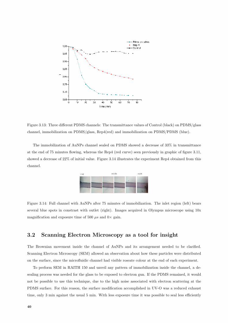
Figure 3.13: Three different PDMS channels: The transmittance values of Control (black) on PDMS/glass
channel, immobilization on PDMS/glass, Rep4(red) and immobilization on PDMS/PDMS (blue).
The immobilization of AuNPs channel sealed on PDMS showed a decrease of 33% in transmittance
at the end of 75 minutes flowing, whereas the Rep4 (red curve) seen previously in graphic of figure 3.11,
showed a decrease of 22% of initial value. Figure 3.14 illustrates the experiment Rep4 obtained from this
channel.
Figure 3.14: Full channel with AuNPs after 75 minutes of immobilization. The inlet region (left) bears
several blue spots in constrast with outlet (right). Images acquired in Olympus microscope using 10x
magnification and exposure time of 500 µs and 0× gain.
3.2 Scanning Electron Microscopy as a tool for insight
The Brownian movement inside the channel of AuNPs and its arrangement needed to be clarified.
Scanning Electron Microscopy (SEM) allowed an observation about how these particles were distributed
on the surface, since the microfluidic channel had visible roseate colour at the end of each experiment.
To perform SEM in RAITH 150 and unveil any pattern of immobilization inside the channel, a de-
sealing process was needed for the glass to be exposed to electron gun. If the PDMS remained, it would
not be possible to use this technique, due to the high noise associated with electron scattering at the
PDMS surface. For this reason, the surface modification accomplished in UV-O was a reduced exhaust
time, only 3 min against the usual 5 min. With less exposure time it was possible to seal less efficiently
40
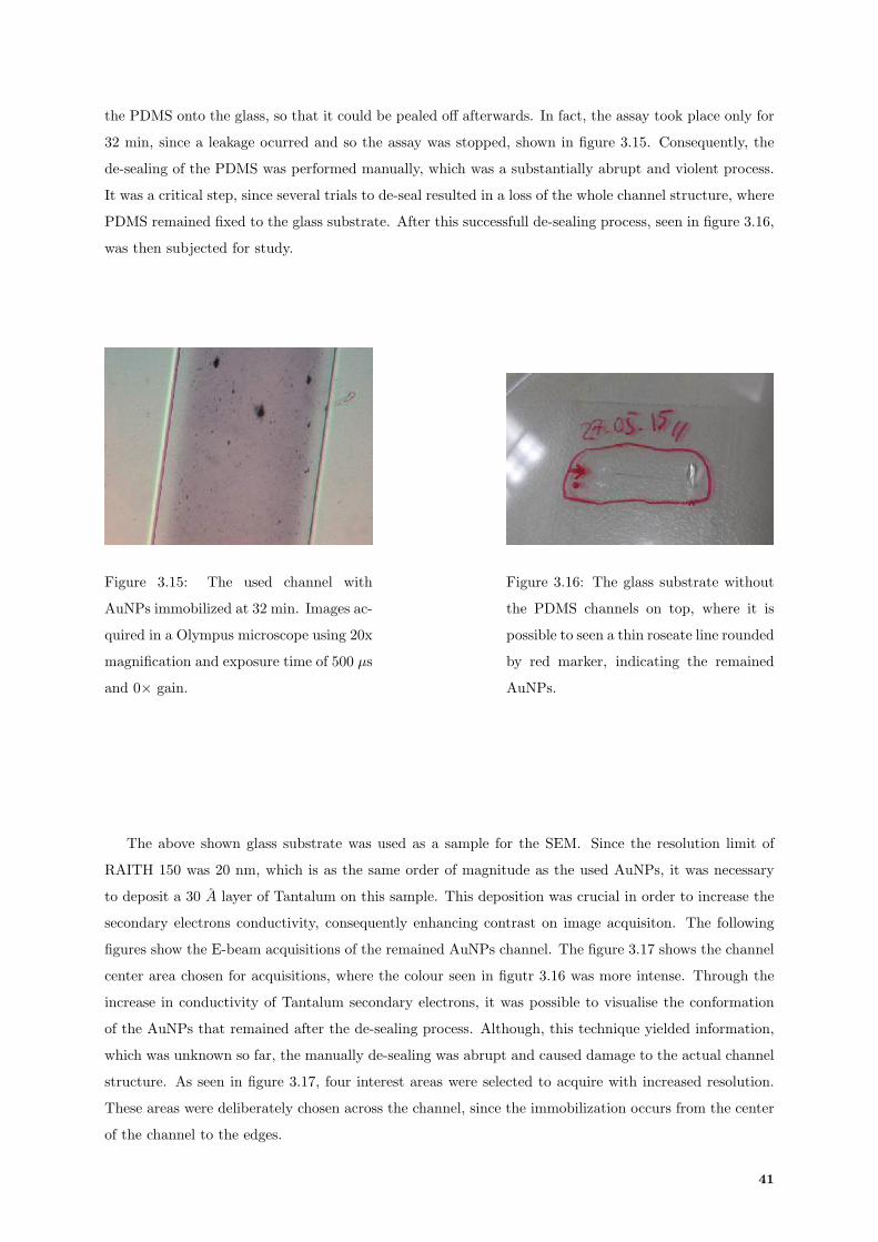
the PDMS onto the glass, so that it could be pealed off afterwards. In fact, the assay took place only for
32 min, since a leakage ocurred and so the assay was stopped, shown in figure 3.15. Consequently, the
de-sealing of the PDMS was performed manually, which was a substantially abrupt and violent process.
It was a critical step, since several trials to de-seal resulted in a loss of the whole channel structure, where
PDMS remained fixed to the glass substrate. After this successfull de-sealing process, seen in figure 3.16,
was then subjected for study.
Figure 3.15: The used channel with
AuNPs immobilized at 32 min. Images ac-
quired in a Olympus microscope using 20x
magnification and exposure time of 500 µs
and 0× gain.
Figure 3.16: The glass substrate without
the PDMS channels on top, where it is
possible to seen a thin roseate line rounded
by red marker, indicating the remained
AuNPs.
The above shown glass substrate was used as a sample for the SEM. Since the resolution limit of
RAITH 150 was 20 nm, which is as the same order of magnitude as the used AuNPs, it was necessary
to deposit a 30 A layer of Tantalum on this sample. This deposition was crucial in order to increase the
secondary electrons conductivity, consequently enhancing contrast on image acquisiton. The following
figures show the E-beam acquisitions of the remained AuNPs channel. The figure 3.17 shows the channel
center area chosen for acquisitions, where the colour seen in figutr 3.16 was more intense. Through the
increase in conductivity of Tantalum secondary electrons, it was possible to visualise the conformation
of the AuNPs that remained after the de-sealing process. Although, this technique yielded information,
which was unknown so far, the manually de-sealing was abrupt and caused damage to the actual channel
structure. As seen in figure 3.17, four interest areas were selected to acquire with increased resolution.
These areas were deliberately chosen across the channel, since the immobilization occurs from the center
of the channel to the edges.
41
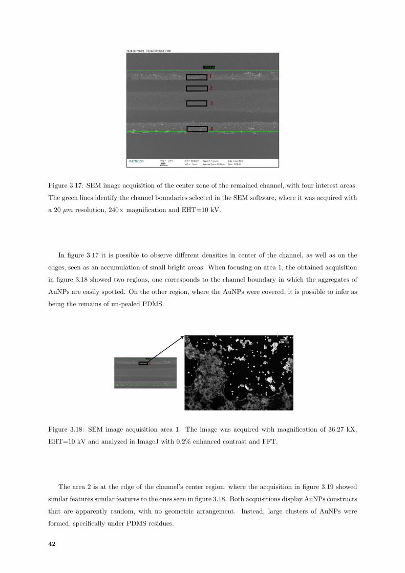
Figure 3.17: SEM image acquisition of the center zone of the remained channel, with four interest areas.
The green lines identify the channel boundaries selected in the SEM software, where it was acquired with
a 20 µm resolution, 240× magnification and EHT=10 kV.
In figure 3.17 it is possible to observe different densities in center of the channel, as well as on the
edges, seen as an accumulation of small bright areas. When focusing on area 1, the obtained acquisition
in figure 3.18 showed two regions, one corresponds to the channel boundary in which the aggregates of
AuNPs are easily spotted. On the other region, where the AuNPs were covered, it is possible to infer as
being the remains of un-pealed PDMS.
Figure 3.18: SEM image acquisition area 1. The image was acquired with magnification of 36.27 kX,
EHT=10 kV and analyzed in ImageJ with 0.2% enhanced contrast and FFT.
The area 2 is at the edge of the channel’s center region, where the acquisition in figure 3.19 showed
similar features similar features to the ones seen in figure 3.18. Both acquisitions display AuNPs constructs
that are apparently random, with no geometric arrangement. Instead, large clusters of AuNPs were
formed, specifically under PDMS residues.
42
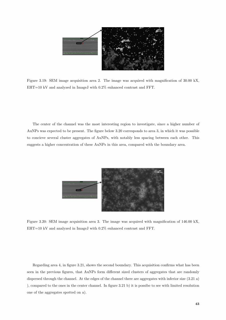
Figure 3.19: SEM image acquisition area 2. The image was acquired with magnification of 30.00 kX,
EHT=10 kV and analyzed in ImageJ with 0.2% enhanced contrast and FFT.
The center of the channel was the most interesting region to investigate, since a higher number of
AuNPs was expected to be present. The figure below 3.20 corresponds to area 3, in which it was possible
to concieve several cluster aggregates of AuNPs, with notably less spacing between each other. This
suggests a higher concentration of these AuNPs in this area, compared with the boundary area.
Figure 3.20: SEM image acquisition area 3. The image was acquired with magnification of 146.00 kX,
EHT=10 kV and analyzed in ImageJ with 0.2% enhanced contrast and FFT.
Regarding area 4, in figure 3.21, shows the second boundary. This acquisition confirms what has been
seen in the previous figures, that AuNPs form different sized clusters of aggregates that are randomly
dispersed through the channel. At the edges of the channel there are aggregates with inferior size (3.21 a)
), compared to the ones in the center channel. In figure 3.21 b) it is possibe to see with limited resolution
one of the aggregates spotted on a).
43
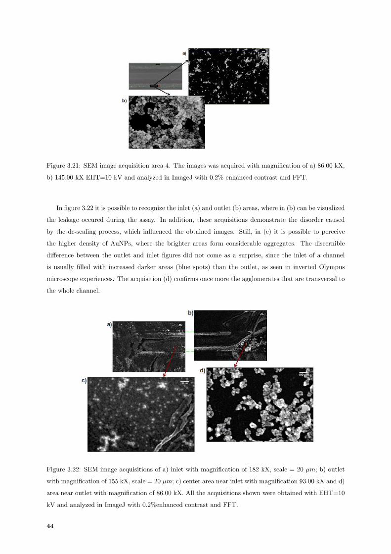
Figure 3.21: SEM image acquisition area 4. The images was acquired with magnification of a) 86.00 kX,
b) 145.00 kX EHT=10 kV and analyzed in ImageJ with 0.2% enhanced contrast and FFT.
In figure 3.22 it is possible to recognize the inlet (a) and outlet (b) areas, where in (b) can be visualized
the leakage occured during the assay. In addition, these acquisitions demonstrate the disorder caused
by the de-sealing process, which influenced the obtained images. Still, in (c) it is possible to perceive
the higher density of AuNPs, where the brighter areas form considerable aggregates. The discernible
difference between the outlet and inlet figures did not come as a surprise, since the inlet of a channel
is usually filled with increased darker areas (blue spots) than the outlet, as seen in inverted Olympus
microscope experiences. The acquisition (d) confirms once more the agglomerates that are transversal to
the whole channel.
Figure 3.22: SEM image acquisitions of a) inlet with magnification of 182 kX, scale = 20 µm; b) outlet
with magnification of 155 kX, scale = 20 µm; c) center area near inlet with magnification 93.00 kX and d)
area near outlet with magnification of 86.00 kX. All the acquisitions shown were obtained with EHT=10
kV and analyzed in ImageJ with 0.2%enhanced contrast and FFT.
44
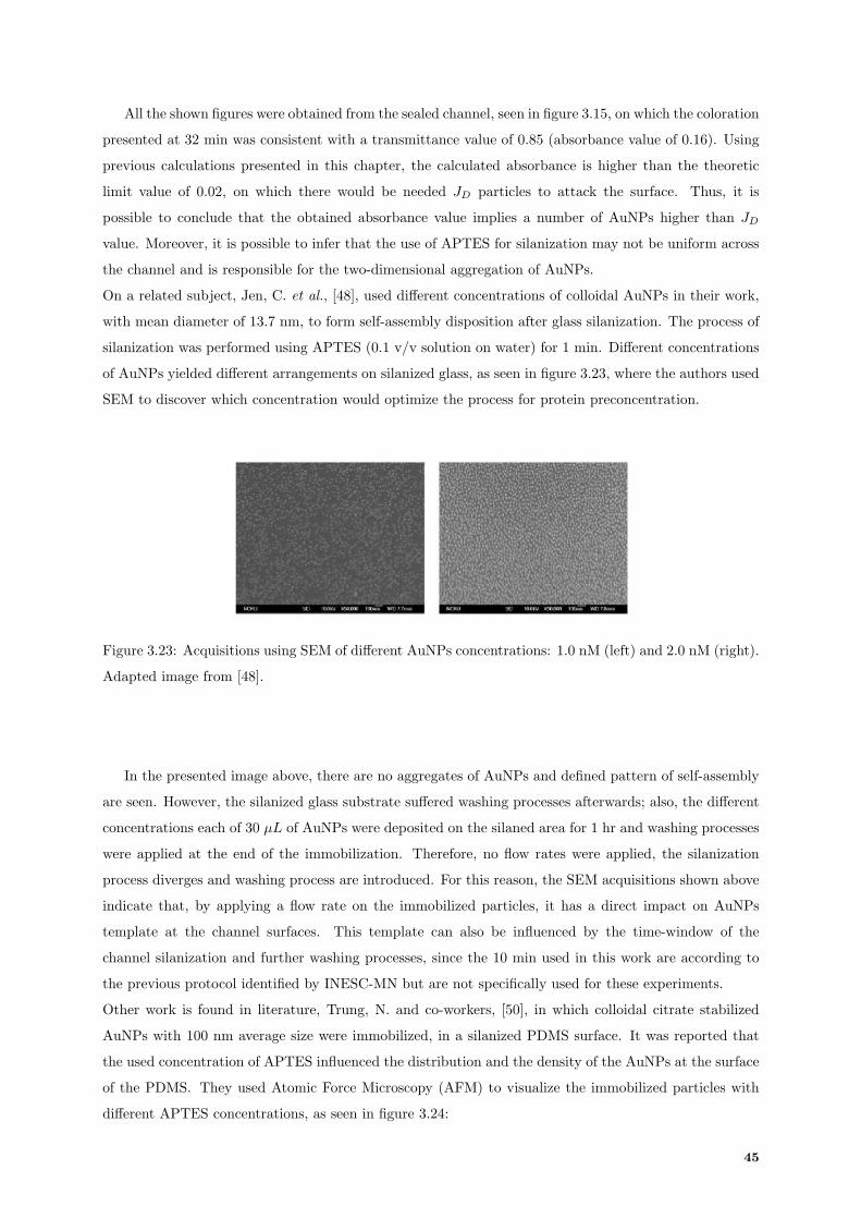
All the shown figures were obtained from the sealed channel, seen in figure 3.15, on which the coloration
presented at 32 min was consistent with a transmittance value of 0.85 (absorbance value of 0.16). Using
previous calculations presented in this chapter, the calculated absorbance is higher than the theoretic
limit value of 0.02, on which there would be needed JD particles to attack the surface. Thus, it is
possible to conclude that the obtained absorbance value implies a number of AuNPs higher than JD
value. Moreover, it is possible to infer that the use of APTES for silanization may not be uniform across
the channel and is responsible for the two-dimensional aggregation of AuNPs.
On a related subject, Jen, C. et al., [48], used different concentrations of colloidal AuNPs in their work,
with mean diameter of 13.7 nm, to form self-assembly disposition after glass silanization. The process of
silanization was performed using APTES (0.1 v/v solution on water) for 1 min. Different concentrations
of AuNPs yielded different arrangements on silanized glass, as seen in figure 3.23, where the authors used
SEM to discover which concentration would optimize the process for protein preconcentration.
Figure 3.23: Acquisitions using SEM of different AuNPs concentrations: 1.0 nM (left) and 2.0 nM (right).
Adapted image from [48].
In the presented image above, there are no aggregates of AuNPs and defined pattern of self-assembly
are seen. However, the silanized glass substrate suffered washing processes afterwards; also, the different
concentrations each of 30 µL of AuNPs were deposited on the silaned area for 1 hr and washing processes
were applied at the end of the immobilization. Therefore, no flow rates were applied, the silanization
process diverges and washing process are introduced. For this reason, the SEM acquisitions shown above
indicate that, by applying a flow rate on the immobilized particles, it has a direct impact on AuNPs
template at the channel surfaces. This template can also be influenced by the time-window of the
channel silanization and further washing processes, since the 10 min used in this work are according to
the previous protocol identified by INESC-MN but are not specifically used for these experiments.
Other work is found in literature, Trung, N. and co-workers, [50], in which colloidal citrate stabilized
AuNPs with 100 nm average size were immobilized, in a silanized PDMS surface. It was reported that
the used concentration of APTES influenced the distribution and the density of the AuNPs at the surface
of the PDMS. They used Atomic Force Microscopy (AFM) to visualize the immobilized particles with
different APTES concentrations, as seen in figure 3.24:
45
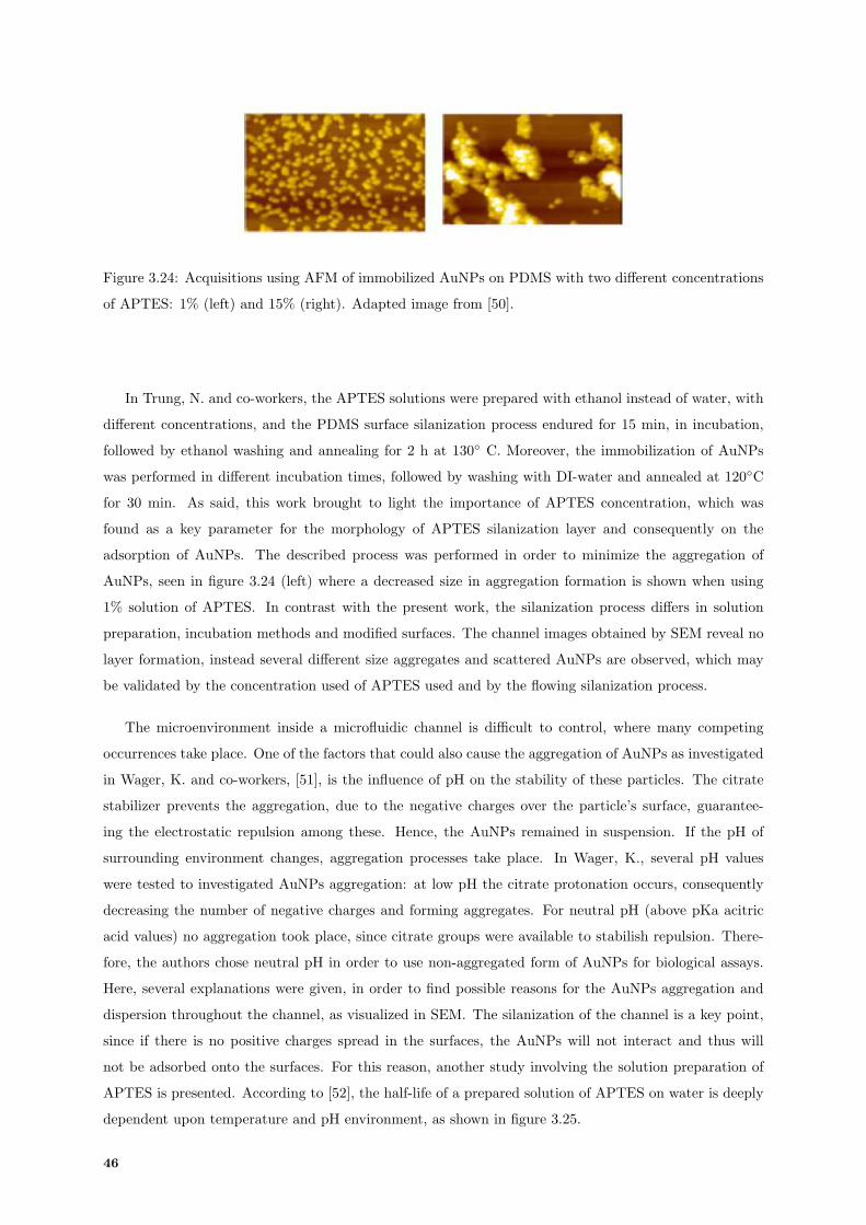
Figure 3.24: Acquisitions using AFM of immobilized AuNPs on PDMS with two different concentrations
of APTES: 1% (left) and 15% (right). Adapted image from [50].
In Trung, N. and co-workers, the APTES solutions were prepared with ethanol instead of water, with
different concentrations, and the PDMS surface silanization process endured for 15 min, in incubation,
followed by ethanol washing and annealing for 2 h at 130 C. Moreover, the immobilization of AuNPs
was performed in different incubation times, followed by washing with DI-water and annealed at 120C
for 30 min. As said, this work brought to light the importance of APTES concentration, which was
found as a key parameter for the morphology of APTES silanization layer and consequently on the
adsorption of AuNPs. The described process was performed in order to minimize the aggregation of
AuNPs, seen in figure 3.24 (left) where a decreased size in aggregation formation is shown when using
1% solution of APTES. In contrast with the present work, the silanization process differs in solution
preparation, incubation methods and modified surfaces. The channel images obtained by SEM reveal no
layer formation, instead several different size aggregates and scattered AuNPs are observed, which may
be validated by the concentration used of APTES used and by the flowing silanization process.
The microenvironment inside a microfluidic channel is difficult to control, where many competing
occurrences take place. One of the factors that could also cause the aggregation of AuNPs as investigated
in Wager, K. and co-workers, [51], is the influence of pH on the stability of these particles. The citrate
stabilizer prevents the aggregation, due to the negative charges over the particle’s surface, guarantee-
ing the electrostatic repulsion among these. Hence, the AuNPs remained in suspension. If the pH of
surrounding environment changes, aggregation processes take place. In Wager, K., several pH values
were tested to investigated AuNPs aggregation: at low pH the citrate protonation occurs, consequently
decreasing the number of negative charges and forming aggregates. For neutral pH (above pKa acitric
acid values) no aggregation took place, since citrate groups were available to stabilish repulsion. There-
fore, the authors chose neutral pH in order to use non-aggregated form of AuNPs for biological assays.
Here, several explanations were given, in order to find possible reasons for the AuNPs aggregation and
dispersion throughout the channel, as visualized in SEM. The silanization of the channel is a key point,
since if there is no positive charges spread in the surfaces, the AuNPs will not interact and thus will
not be adsorbed onto the surfaces. For this reason, another study involving the solution preparation of
APTES is presented. According to [52], the half-life of a prepared solution of APTES on water is deeply
dependent upon temperature and pH environment, as shown in figure 3.25.
46
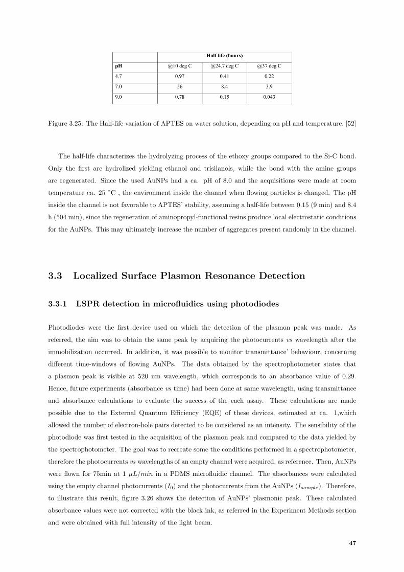
Figure 3.25: The Half-life variation of APTES on water solution, depending on pH and temperature. [52]
The half-life characterizes the hydrolyzing process of the ethoxy groups compared to the Si-C bond.
Only the first are hydrolized yielding ethanol and trisilanols, while the bond with the amine groups
are regenerated. Since the used AuNPs had a ca. pH of 8.0 and the acquisitions were made at room
temperature ca. 25 C , the environment inside the channel when flowing particles is changed. The pH
inside the channel is not favorable to APTES’ stability, assuming a half-life between 0.15 (9 min) and 8.4
h (504 min), since the regeneration of aminopropyl-functional resins produce local electrostatic conditions
for the AuNPs. This may ultimately increase the number of aggregates present randomly in the channel.
3.3 Localized Surface Plasmon Resonance Detection
3.3.1 LSPR detection in microfluidics using photodiodes
Photodiodes were the first device used on which the detection of the plasmon peak was made. As
referred, the aim was to obtain the same peak by acquiring the photocurrents vs wavelength after the
immobilization occurred. In addition, it was possible to monitor transmittance’ behaviour, concerning
different time-windows of flowing AuNPs. The data obtained by the spectrophotometer states that
a plasmon peak is visible at 520 nm wavelength, which corresponds to an absorbance value of 0.29.
Hence, future experiments (absorbance vs time) had been done at same wavelength, using transmittance
and absorbance calculations to evaluate the success of the each assay. These calculations are made
possible due to the External Quantum Efficiency (EQE) of these devices, estimated at ca. 1,which
allowed the number of electron-hole pairs detected to be considered as an intensity. The sensibility of the
photodiode was first tested in the acquisition of the plasmon peak and compared to the data yielded by
the spectrophotometer. The goal was to recreate some the conditions performed in a spectrophotometer,
therefore the photocurrents vs wavelengths of an empty channel were acquired, as reference. Then, AuNPs
were flown for 75min at 1 µL/min in a PDMS microfluidic channel. The absorbances were calculated
using the empty channel photocurrents (I0) and the photocurrents from the AuNPs (Isample). Therefore,
to illustrate this result, figure 3.26 shows the detection of AuNPs’ plasmonic peak. These calculated
absorbance values were not corrected with the black ink, as referred in the Experiment Methods section
and were obtained with full intensity of the light beam.
47
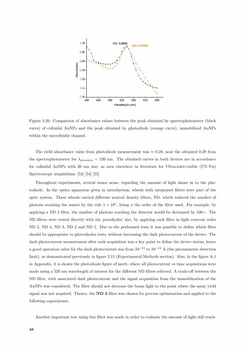
Figure 3.26: Comparison of absorbance values between the peak obtained by spectrophotometer (black
curve) of colloidal AuNPs and the peak obtained by photodiode (orange curve), immobilized AuNPs
within the microfluidic channel.
The yield absorbance value from photodiode measurement was ≈ 0.28, near the obtained 0.29 from
the spectrophotometer for λplasmon = 520 nm. The obtained curves in both devices are in accordance
for colloidal AuNPs with 20 nm size, as seen elsewhere in literature for Ultraviolet-visible (UV-Vis)
Spectroscopy acquisitions. [53] [54] [55]
Throughout experiments, several issues arose, regarding the amount of light shone in to the pho-
todiode. In the optics apparatus given in introduction, wheels with integrated filters were part of the
optic system. These wheels carried different neutral density filters, ND, which reduced the number of
photons reaching the sensor by the rule 1 × 10x, being x the order of the filter used. For example, by
applying a ND 2 filter, the number of photons reaching the detector would be decreased by 100×. The
ND filters were tested directly with the potodiodes’ dye, by applying each filter in light crescent order
ND 5, ND 4, ND 3, ND 2 and ND 1. Due to the performed tests it was possible to define which filter
should be appropriate to photodiodes tests, without increasing the dark photocurrent of the device. The
dark photocurrent measurement after each acquisition was a key point to define the device status, hence
a good operation value for the dark photocurrent was from 10−13 to 10−14 A (the picoammeter detection
limit), as demonstrated previously in figure 2.11 (Experimental Methods section). Also, in the figure A.1
in Appendix, it is shown the photodiode figure of merit, where all photocurrent vs time acquisitions were
made using a 520 nm wavelength of interest for the different ND filters referred. A trade-off between the
ND filter, with associated dark photocurrent and the signal acquisition from the immobilization of the
AuNPs was considered. The filter should not decrease the beam light to the point where the assay yield
signal was not acquired. Thence, the ND 3 filter was chosen for process optimization and applied to the
following experiments.
Another important test using this filter was made in order to evaluate the amount of light still reach-
48
ing the photodiode, when a channel was filled with black ink. The figure A.2 in Appendix shows the
acquisition of photocurrent in function of time, measured at 520 nm. A black ink channel yield an output
photocurrent of order ≈ 10−11A, being two orders of magnitude higher compared to the dark photocur-
rent measured. With this experiment an expected result would be an output photocurrent of ≈ 10−13A,
since the channel was filled with black ink and subjected to an incident light beam with 1000x less inten-
sity. The possible contributions to higher photocurrent values acquired may be sourced on the scattered
light occured in the PDMS structure and black ink interaction with channel surfaces. Furthermore, the
black ink channel acquisitions were irregular, these values suggest that the black ink was not completely
opaque when a small volume was introduced in the channel, causing the incident and scattered light to
reach the detector.
In each experiment accomplished, the essential steps in protocol were followed:
• Dark Photocurrent vs Bias Voltage (V);
• Dark Photocurrent vs time;
• ND 3 photocurrent acquisition and beam alignment;
• Photocurrents (in function of time and spectrum) acquisition of an empty PDMS channel;
• Photocurrents acquisition while (time) and after (spectrum) flowing APTES;
• Photocurrents acquisition while (time) and after (spectrum) flowing AuNPs;
• Photocurrents acquisition of channel filled with black ink;
• Dark Photocurrent vs time;
These steps were followed to observe if the spectrum of an empty channel and of APTES filled channel
were almost coincident, since the air’s index of refraction is ≈ 1.00 and APTES is 1.43 (at 20 C). [56]
The next immobilization of AuNPs for 30 min was performed and its spectrum was acquired. As expected
the spectrum shows a decrease in photocurrent when compared to the APTES, however this decrease is
not uniform, by which for smaller wavelengths from 450 nm and higher ones from 600 nm, the spectra
are coincident, as shown in figure A.3 in Appendix. Through spectra acquisitions it was possible to
calculate the absorbance values, using photocurrent acquisitions of the flown APTES as reference. The
calculations were corrected with photocurrent values from black ink acquisition and plotted in figure 3.27.
As seen in the figure below, it is not similar to the initial absorbances calculated reported by spectroscopy
value in figure 3.26. This experiment was however subjected to a different approach: a ND 3 filter was
used, AuNPs were flown at 1 µL/min for only 30 min and the calculated values were corrected with
a black ink channel. There is no evident plasmonic peak in this figure, only a higher value is spotted
at 555 nm. Although the raw data seen in figure A.3 in Appendix, shows differences in photocurrent
intensities from APTES to AuNPs, whereas a theoretical absorbance of 0.12 is expected, the analysis of
data yields a value of 0.21. This can be explained by the correction with black ink, that is subtracted to
both acquisitions I0 and Isample so, when transmittance is calculated by the ratio of the two, it yields a
49
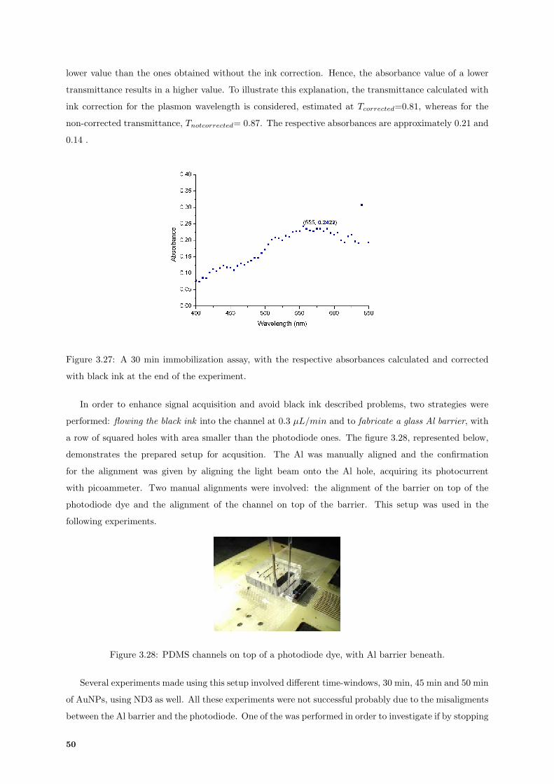
lower value than the ones obtained without the ink correction. Hence, the absorbance value of a lower
transmittance results in a higher value. To illustrate this explanation, the transmittance calculated with
ink correction for the plasmon wavelength is considered, estimated at Tcorrected=0.81, whereas for the
non-corrected transmittance, Tnotcorrected= 0.87. The respective absorbances are approximately 0.21 and
0.14 .
Figure 3.27: A 30 min immobilization assay, with the respective absorbances calculated and corrected
with black ink at the end of the experiment.
In order to enhance signal acquisition and avoid black ink described problems, two strategies were
performed: flowing the black ink into the channel at 0.3 µL/min and to fabricate a glass Al barrier, with
a row of squared holes with area smaller than the photodiode ones. The figure 3.28, represented below,
demonstrates the prepared setup for acqusition. The Al was manually aligned and the confirmation
for the alignment was given by aligning the light beam onto the Al hole, acquiring its photocurrent
with picoammeter. Two manual alignments were involved: the alignment of the barrier on top of the
photodiode dye and the alignment of the channel on top of the barrier. This setup was used in the
following experiments.
Figure 3.28: PDMS channels on top of a photodiode dye, with Al barrier beneath.
Several experiments made using this setup involved different time-windows, 30 min, 45 min and 50 min
of AuNPs, using ND3 as well. All these experiments were not successful probably due to the misaligments
between the Al barrier and the photodiode. One of the was performed in order to investigate if by stopping
50
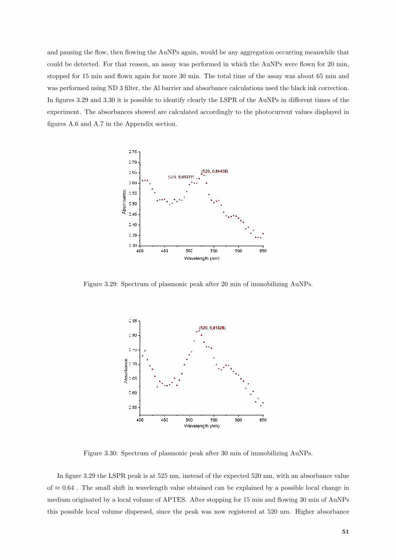
and pausing the flow, then flowing the AuNPs again, would be any aggregation occurring meanwhile that
could be detected. For that reason, an assay was performed in which the AuNPs were flown for 20 min,
stopped for 15 min and flown again for more 30 min. The total time of the assay was about 65 min and
was performed using ND 3 filter, the Al barrier and absorbance calculations used the black ink correction.
In figures 3.29 and 3.30 it is possible to identify clearly the LSPR of the AuNPs in different times of the
experiment. The absorbances showed are calculated accordingly to the photocurrent values displayed in
figures A.6 and A.7 in the Appendix section.
Figure 3.29: Spectrum of plasmonic peak after 20 min of immobilizing AuNPs.
Figure 3.30: Spectrum of plasmonic peak after 30 min of immobilizing AuNPs.
In figure 3.29 the LSPR peak is at 525 nm, instead of the expected 520 nm, with an absorbance value
of ≈ 0.64 . The small shift in wavelength value obtained can be explained by a possible local change in
medium originated by a local volume of APTES. After stopping for 15 min and flowing 30 min of AuNPs
this possible local volume dispersed, since the peak was now registered at 520 nm. Higher absorbance
51
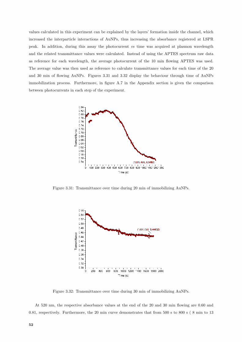
values calculated in this experiment can be explained by the layers’ formation inside the channel, which
increased the interparticle interactions of AuNPs, thus increasing the absorbance registered at LSPR
peak. In addition, during this assay the photocurrent vs time was acquired at plasmon wavelength
and the related transmittance values were calculated. Instead of using the APTES spectrum raw data
as reference for each wavelength, the average photocurrent of the 10 min flowing APTES was used.
The average value was then used as reference to calculate transmittance values for each time of the 20
and 30 min of flowing AuNPs. Figures 3.31 and 3.32 display the behaviour through time of AuNPs
immobilization process. Furthermore, in figure A.7 in the Appendix section is given the comparison
between photocurrents in each step of the experiment.
Figure 3.31: Transmittance over time during 20 min of immobilizing AuNPs.
Figure 3.32: Transmittance over time during 30 min of immobilizing AuNPs.
At 520 nm, the respective absorbance values at the end of the 20 and 30 min flowing are 0.60 and
0.81, respectively. Furthermore, the 20 min curve demonstrates that from 500 s to 800 s ( 8 min to 13
52

min) there is a ≈ 15 % decrease in transmittance from initial value of measured with APTES solution
at the beginning of the experiment. This similar decreasing behaviour is in accordance with what was
already seen in Figure 3.1, in Olympus Microscope assays. This transmittance curve differs from the
results showed in Figure 3.1 at the beginning of the assay, since the transmittance value at 0 s is not
1. Moreover, the final transmittance value of 20 min assay is 0.54, which is the same transmittance
value that the 30 min starts with, suggesting that the 15 min stop between flowing did not affect the
environment inside the channel. At the beginning of the assay in figure 3.31, the transmittance suffered
an abrupt variation in the 100 s of flowing, possibly due to the presence of local air bubbles that remained
in the sensor area of detection, being removed by the movement of the liquid itself.
Other experiments were made in order to reproduce this results in a 75 min time-window assay, al-
though they were not successful. One of the experiments made was the PBS washing experiment using the
referred conditions, the photocurrent values obtained for each wavelength of the immobilization, followed
by washing were coincident, implying the strength of the electrostatic interaction of AuNPs and APTES.
However, the absorbance value of the LSPR was not possible to identify. In the experiments performed,
the setup used with the Al proven to be as much challenging as crucial to the success of the assay. The
two manual alignments made are potentially the source of error introduced in the acquisition, a part from
other non-controlled factors such as the surface chemistry performed on the channel surfaces. The suc-
cessful acquisition represented in figure 3.26 with no light barrier, no ND filter and using photocurrents
from the initial empty channel as reference was the landmark for comparison. These conditions were
not repeated since the device would increase its dark current, affecting the following acquisitions, and
also the scattered light would contribute to a higher signal output. Hence, the further conditions used,
such as ND 3 filter, the ink correction and the barrier to protect from scattered light are justified, but
demanding to be reproducible. Whilst the experiments made, the system showed great sensitivity, since
the obtained spectra did not present a smooth curve, instead a ripple behaviour, showing that there is
still noise introduced in the acquisition.
3.3.2 LSPR detection in microfluidics using photoconductors
The photoconductor experiments were engaged to investigate if the results described in the previous
section would still be confirmed using these devices instead. The protocol of the immobilization followed
the previously described steps: 10 min of surface silanization (APTES) and flowing the AuNPs at 1
µL/min. Due to the operating nature of these devices, an external voltage was applied in the ranges of [10-
30] V. The ensuing results build a path on the optimization of LSPR acquisition using photoconductors.In
order to obtain a higher order of magnitude signal from the experiment, in comparison with the dark and
black ink photocurrents seen in Appendix figures A.8, one of the first experiments using these devices
was to perform a 30 min immobilization of AuNPs, using the Al barrier aligned to the photoconductor
dye as well. This experiment aimed to compare with described results using photodiodes, but also to
inquire if the tradeoff between acquiring higher output signal and the scattered light interference was also
significant. Therefore, a full light beam ( ND 0 filter) and black ink correction data were used at the end
53
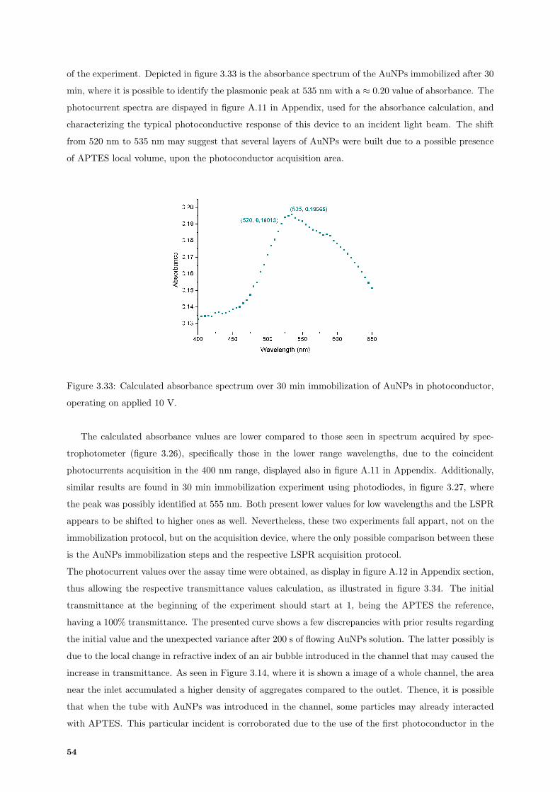
of the experiment. Depicted in figure 3.33 is the absorbance spectrum of the AuNPs immobilized after 30
min, where it is possible to identify the plasmonic peak at 535 nm with a ≈ 0.20 value of absorbance. The
photocurrent spectra are dispayed in figure A.11 in Appendix, used for the absorbance calculation, and
characterizing the typical photoconductive response of this device to an incident light beam. The shift
from 520 nm to 535 nm may suggest that several layers of AuNPs were built due to a possible presence
of APTES local volume, upon the photoconductor acquisition area.
Figure 3.33: Calculated absorbance spectrum over 30 min immobilization of AuNPs in photoconductor,
operating on applied 10 V.
The calculated absorbance values are lower compared to those seen in spectrum acquired by spec-
trophotometer (figure 3.26), specifically those in the lower range wavelengths, due to the coincident
photocurrents acquisition in the 400 nm range, displayed also in figure A.11 in Appendix. Additionally,
similar results are found in 30 min immobilization experiment using photodiodes, in figure 3.27, where
the peak was possibly identified at 555 nm. Both present lower values for low wavelengths and the LSPR
appears to be shifted to higher ones as well. Nevertheless, these two experiments fall appart, not on the
immobilization protocol, but on the acquisition device, where the only possible comparison between these
is the AuNPs immobilization steps and the respective LSPR acquisition protocol.
The photocurrent values over the assay time were obtained, as display in figure A.12 in Appendix section,
thus allowing the respective transmittance values calculation, as illustrated in figure 3.34. The initial
transmittance at the beginning of the experiment should start at 1, being the APTES the reference,
having a 100% transmittance. The presented curve shows a few discrepancies with prior results regarding
the initial value and the unexpected variance after 200 s of flowing AuNPs solution. The latter possibly is
due to the local change in refractive index of an air bubble introduced in the channel that may caused the
increase in transmittance. As seen in Figure 3.14, where it is shown a image of a whole channel, the area
near the inlet accumulated a higher density of aggregates compared to the outlet. Thence, it is possible
that when the tube with AuNPs was introduced in the channel, some particles may already interacted
with APTES. This particular incident is corroborated due to the use of the first photoconductor in the
54

used dye, which was aligned closely to the inlet of the channel.
Figure 3.34: Transmittance calculated values of 30 min immobilization acquired in photoconductor,
operating on applied 10 V.
Still in the same experiment, another interaction was put to the test. After flowing the AuNPs
immobilization, Bovine Serum Albumine (BSA) 4% solution was flown for 10 min at 0.5 µL/min flow
rate, according to previous work at INESC-MN. The yield absorbance spectrum is shown in figure 3.35,
where it is easily identified the plasmonic peak at 525 nm wavelength with an absorbance value of ≈
0.56. The curve obtained is analogous to the one obtained in figure 3.26 using photodiodes, although
the presented values are higher for the interaction of BSA and the AuNPs. These higher values can be
originated by the increased hindrance to light passage which originated low photocurrents acquisition,
since the protein interaction and binding to the AuNPs occurred throughout the channel surfaces. Thus,
when the photocurrent was acquired it presents a lower value than the initial yielded from the AuNPs
immobilization. Apparently, the adsorption of BSA on the AuNPs did not introduce a variation in the
refraction index, by which a shift to higher wavelengths would have been seen.
55
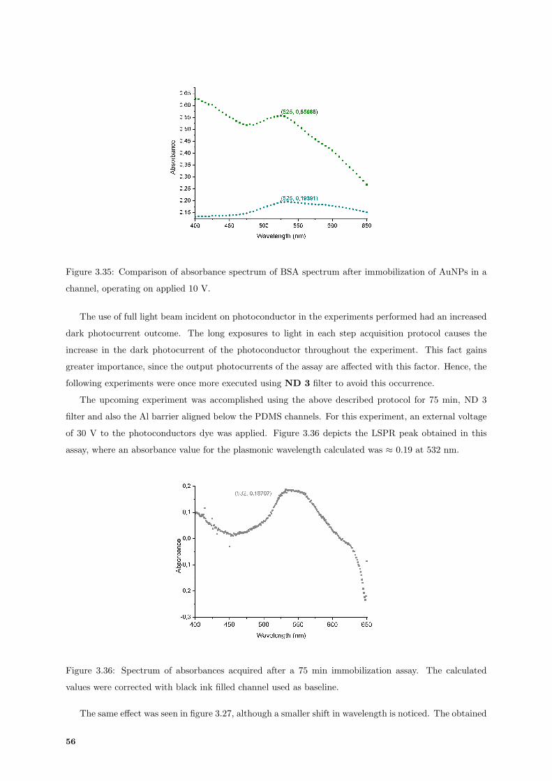
Figure 3.35: Comparison of absorbance spectrum of BSA spectrum after immobilization of AuNPs in a
channel, operating on applied 10 V.
The use of full light beam incident on photoconductor in the experiments performed had an increased
dark photocurrent outcome. The long exposures to light in each step acquisition protocol causes the
increase in the dark photocurrent of the photoconductor throughout the experiment. This fact gains
greater importance, since the output photocurrents of the assay are affected with this factor. Hence, the
following experiments were once more executed using ND 3 filter to avoid this occurrence.
The upcoming experiment was accomplished using the above described protocol for 75 min, ND 3
filter and also the Al barrier aligned below the PDMS channels. For this experiment, an external voltage
of 30 V to the photoconductors dye was applied. Figure 3.36 depicts the LSPR peak obtained in this
assay, where an absorbance value for the plasmonic wavelength calculated was ≈ 0.19 at 532 nm.
Figure 3.36: Spectrum of absorbances acquired after a 75 min immobilization assay. The calculated
values were corrected with black ink filled channel used as baseline.
The same effect was seen in figure 3.27, although a smaller shift in wavelength is noticed. The obtained
56
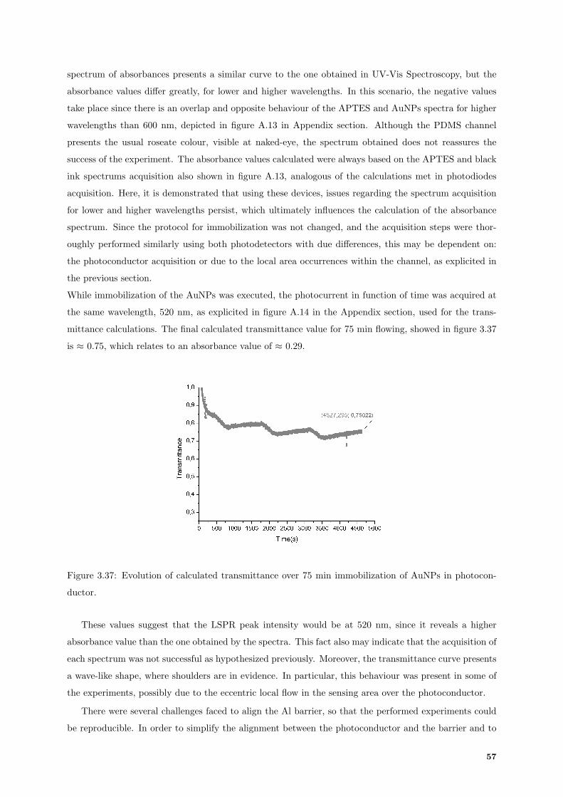
spectrum of absorbances presents a similar curve to the one obtained in UV-Vis Spectroscopy, but the
absorbance values differ greatly, for lower and higher wavelengths. In this scenario, the negative values
take place since there is an overlap and opposite behaviour of the APTES and AuNPs spectra for higher
wavelengths than 600 nm, depicted in figure A.13 in Appendix section. Although the PDMS channel
presents the usual roseate colour, visible at naked-eye, the spectrum obtained does not reassures the
success of the experiment. The absorbance values calculated were always based on the APTES and black
ink spectrums acquisition also shown in figure A.13, analogous of the calculations met in photodiodes
acquisition. Here, it is demonstrated that using these devices, issues regarding the spectrum acquisition
for lower and higher wavelengths persist, which ultimately influences the calculation of the absorbance
spectrum. Since the protocol for immobilization was not changed, and the acquisition steps were thor-
oughly performed similarly using both photodetectors with due differences, this may be dependent on:
the photoconductor acquisition or due to the local area occurrences within the channel, as explicited in
the previous section.
While immobilization of the AuNPs was executed, the photocurrent in function of time was acquired at
the same wavelength, 520 nm, as explicited in figure A.14 in the Appendix section, used for the trans-
mittance calculations. The final calculated transmittance value for 75 min flowing, showed in figure 3.37
is ≈ 0.75, which relates to an absorbance value of ≈ 0.29.
Figure 3.37: Evolution of calculated transmittance over 75 min immobilization of AuNPs in photocon-
ductor.
These values suggest that the LSPR peak intensity would be at 520 nm, since it reveals a higher
absorbance value than the one obtained by the spectra. This fact also may indicate that the acquisition of
each spectrum was not successful as hypothesized previously. Moreover, the transmittance curve presents
a wave-like shape, where shoulders are in evidence. In particular, this behaviour was present in some of
the experiments, possibly due to the eccentric local flow in the sensing area over the photoconductor.
There were several challenges faced to align the Al barrier, so that the performed experiments could
be reproducible. In order to simplify the alignment between the photoconductor and the barrier and to
57
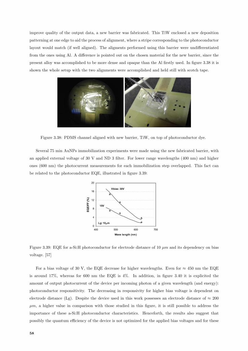
improve quality of the output data, a new barrier was fabricated. This TiW enclosed a new deposition
patterning at one edge to aid the process of alignment, where a stripe corresponding to the photoconductor
layout would match (if well aligned). The aligments performed using this barrier were undifferentiated
from the ones using Al. A difference is pointed out on the chosen material for the new barrier, since the
present alloy was accomplished to be more dense and opaque than the Al firstly used. In figure 3.38 it is
shown the whole setup with the two alignments were accomplished and held still with scotch tape.
Figure 3.38: PDMS channel aligned with new barrier, TiW, on top of photoconductor dye.
Several 75 min AuNPs immobilization experiments were made using the new fabricated barrier, with
an applied external voltage of 30 V and ND 3 filter. For lower range wavelengths (400 nm) and higher
ones (600 nm) the photocurrent measurements for each immobilization step overlapped. This fact can
be related to the photoconductor EQE, illustrated in figure 3.39:
Figure 3.39: EQE for a-Si:H photoconductor for electrode distance of 10 µm and its dependency on bias
voltage. [57]
For a bias voltage of 30 V, the EQE decrease for higher wavelengths. Even for ≈ 450 nm the EQE
is around 17%, whereas for 600 nm the EQE is 4%. In addition, in figure 3.40 it is explicited the
amount of output photocurrent of the device per incoming photon of a given wavelength (and energy):
photoconductor responsitivity. The decreasing in responsivity for higher bias voltage is dependent on
electrode distance (Lg). Despite the device used in this work possesses an electrode distance of ≈ 200
µm, a higher value in comparison with those studied in this figure, it is still possible to address the
importance of these a-Si:H photoconductor characteristics. Henceforth, the results also suggest that
possibly the quantum efficiency of the device is not optimized for the applied bias voltages and for these
58

wavelengths.
Figure 3.40: Responsivity of a-Si:H photoconductor and dependency on electrode spacing. [57]
None of the performed experiments was successful with the new barrier, as the acquired photocurrent
showed a high degree of variation in each acquisition value, seen in figure A.15 in the Appendix section,
ultimately resulting in no LSPR peak detection. The photocurrent values obtained recursively revealed a
scattered acquisition spectra, however in some assays there was no overlap of the spectrum acquisitions,
and only the scattered values were acquired with no typical shape of the photoconductive response. This
scattered acquisition may the result of an increase in defect density due to the increase of light exposure.
This would reduce the efficiency in the conversion of incident light into photocurrent.
59

60

4Conclusions and Future Challenges
Contents
Bibliography . . . . . . . . . . . . . . . . . . . . . . . . . . . . . . . . . . . . . . . . . 67
4.1 References . . . . . . . . . . . . . . . . . . . . . . . . . . . . . . . . . . . . . . . 67
61
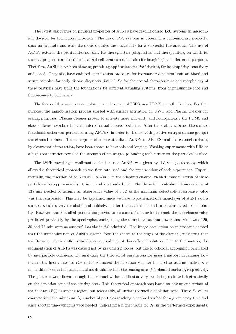
The latest discoveries on physical properties of AuNPs have revolutionized LoC systems in microflu-
idic devices, for biomarkers detection. The use of PoC systems is becoming a contemporary necessity,
since an accurate and early diagnosis dictates the probability for a successful therapeutic. The use of
AuNPs extends the possibilities not only for theragnostics (diagnostics and therapeutics), on which its
thermal properties are used for localized cell treatments, but also for imagiologic and detection purposes.
Therefore, AuNPs have been showing promising applications for PoC devices, for its simplicity, sensitivity
and speed. They also have endured optimization processes for biormarker detection limit on blood and
serum samples, for early disease diagnosis. [58] [59] So far the optical characteristics and morphology of
these particles have built the foundations for different signaling systems, from chemiluminescence and
fluorescence to colorimetry.
The focus of this work was on colorimetric detection of LSPR in a PDMS microfluidic chip. For that
purpose, the immobilization process started with surface activation on UV-O and Plasma Cleaner for
sealing purposes. Plasma Cleaner proven to activate more efficiently and homogenously the PDMS and
glass surfaces, avoiding the encountered initial leakage problems. After the sealing process, the surface
functionalization was performed using APTES, in order to silanize with positive charges (amine groups)
the channel surfaces. The adsorption of citrate stabilized AuNPs to APTES modified channel surfaces,
by electrostatic interaction, have been shown to be stable and longing. Washing experiments with PBS at
a high concentration revealed the strength of amine groups binding with citrate on the particles’ surface.
The LSPR wavelength confirmation for the used AuNPs was given by UV-Vis spectroscopy, which
allowed a theoretical approach on the flow rate used and the time-window of each experiment. Experi-
mentally, the insertion of AuNPs at 1 µL/min in the silanized channel yielded immobilization of these
particles after approximately 10 min, visible at naked eye. The theoretical calculated time-window of
135 min needed to acquire an absorbance value of 0.02 as the minimum detectable absorbance value
was then surpassed. This may be explained since we have hypothesized one monolayer of AuNPs on a
surface, which is very irrealistic and unlikely, but for the calculations had to be considered for simplic-
ity. However, these studied parameters proven to be successful in order to reach the absorbance value
predicted previously by the spectrophotomete, using the same flow rate and lower time-windows of 20,
30 and 75 min were as successful as the initial admitted. The image acquisition on microscope showed
that the immobilization of AuNPs started from the center to the edges of the channel, indicating that
the Brownian motion affects the dispersion stability of this colloidal solution. Due to this motion, the
sedimentation of AuNPs was caused not by gravimetric forces, but due to colloidal aggregation originated
by interparticle collisions. By analyzing the theoretical parameters for mass transport in laminar flow
regime, the high values for PeS and PeH implied the depletion zone for the electrostatic interaction was
much thinner than the channel and much thinner that the sensing area (Wc channel surface), respectively.
The particles were flown through the channel without diffusion very far, being collected electrostically
on the depletion zone of the sensing area. This theoretical approach was based on having one surface of
the channel (Wc) as sensing region, but reasonably, all surfaces formed a depletion zone. These Pe values
characterized the minimum JD number of particles reaching a channel surface for a given assay time and
since shorter time-windows were needed, indicating a higher value for JD in the performed experiments.
62
The environment inside the channel was later visualized using SEM, through the abrupt de-sealing
of PDMS from the glass surface. This allowed an analysis to the recursive appearance of blue-coloured
”spots” while flowing AuNPs. These ”blue spots” were conceived to be substantial aggregates of AuNPs,
different sized and randomly distributed in the channel, in which by further analysis it was positively
confirmed. With the use of this technique, it was possible to obtain 20 nm resolution images of the glass
surface areas, with prior Tantalum deposition. Although the usual methods seen for the visualization
of AuNPs morphology and organization are AFM and Transmission Electron Microscopy, the performed
SEM visualization of the immobilized AuNPs was still successful. Some questions arose regarding the
de-sealing process affecting the initial environment, by which conclusions taken from the glass surface
visualization would be compromised. However, as referred formerly, several studies confirm particle
aggregation of AuNPs in many assay conditions.
The LSPR detection in a microfluidic channel was performed using 200 µm sq. photodiodes and
photoconductors, aligned below of the microfluidic chip. The experiments were subjected to several mod-
ifications, since many issues regarding scattered light as source of noise emerged in current acquisitions.
Both setups used were coupled with two fabricated light barriers, in order to decrease the incoming
scattered light. The inherent problems regarding the barriers were mainly about manual misalignments
between the barriers and the devices, also between the barriers and the PDMS channels. In addition,
the possible misaligments of the light beam and the whole setup were also considered. Throughout the
assays, the acqusition system proven to be very sensitive, embedding noise not only from light, but also
from external sources, such as the introduction of liquids in the channel by the syringe pump and from
the acquisition room itself. Furthermore, a black ink was used, as a measure of the amount of light still
reaching the photodetector, to fill the channel at assay terminus so that the output data could be cor-
rected afterwards. The black ink purchased revealed high hydrophobic behaviour towards the channels’
surfaces, causing a non-homogenous spreading in the channel. These factors arise as the black ink was
chosen for data baseline correction throughout experiments, since it revealed some problems regarding
acquisition reproducibility, which was far from being accomplished. Therefore, the spectra obtained in
each experiment diverged in shape and in value. The figure A.4 in Appendix demonstrates the compar-
ison between the spectrum acquisition made previously seen in figure A.3 and another empty channel
filled only with black ink. Moreover, it is shown that while acquiring the correspondent photocurrent of
a black ink-filled channel I(t), the ink was removed partially in the channel to the outlet, due to own
hydrophobicity towards the PDMS and glass surfaces, as seen in figure A.5 also in Appendix section.
Since the ink was not flown and only initially introduced, the removal occurred repeatedly along the
experiments, implying that the ink itself appeared to build no adhesion to channel surfaces. Moreover,
by observing figure A.4 and its values, it proposes the possibility that the interaction between the ink
and the AuNPs differs from the ink filled channel, due to the fact that the channel filled with AuNPs
has less available ”free path” than the latter. Then, when the channel with particles is filled with ink
local irregularites are created that allow the light to enter and scatter inside the channel, thus increasing
photocurrent acquisition. This fact was visible in considerable experiments, where the spectrum and
current acquisitions were skewed, ultimately causing high variations in data analysis.
63
The AuNPs spectrum of absorbances acquired in spectrophotometer and photodiode, seen in figure
3.26, represent the acquisition capability of this photodetector, on which no ND filter and light barrier were
used. The success of the following experiments was compared with this result and evaluated accordingly.
In photodiodes, the plasmonic peak was successfully acquired by immobilizing the AuNPs in the 75 min
(figure 3.26), 20 min and 30 min assays (figures 3.29 and 3.30, respectively), with conclusive absorbances
calculated. In many experiments performed, the output spectra were analogous to the obtained figure
3.27, where the peak was poorly evident and the spectrum boundaries do not follow the observed trend
seen in figure 3.26 . So far, in order to obtain a successful absorbance spectra spectra, a full-wavelength
decrease is needed in photocurrent acquisition, compared with the photocurrent acquisition from the
APTES measurement, as e.g. see Appendix figures A.6 and A.7. In some experiments the overlap of
both photocurrent spectra (APTES and AuNPs) can be explained with the results obtained in SEM
acquisitions. There were different sized and randomly spaced aggregates of AuNPs, regardless the de-
sealing experiment being abrupt and possibly introduced a chaotic environment. Let it be assumed that
inside the channel, prior to the de-sealing, there were aggregates with different size formed dispersed
through the surfaces inside the channel. This random and spaced aggregates can coincide with the
location of the photodiode area, where locally the volume itself is not filled with JD number of particles.
This fact suggests that when the spectrum acquisition begins for higher and finishes for lower wavelengths,
the resident AuNPs and the remained APTES interactions contribute to the overlap of the two spectra.
Although, for the wavelength range of biological interest (500-540) nm of this AuNPs size, the contribution
of the dispersed AuNPs increases, due to the LSPR. As claimed, the typical absorbance spectrum of
AuNPs is possible to obtain using photodiodes, therefore the unsuccessful experiments were possibly a
result from misalignments of the barrier, between the device and the PDMS channels; possibly due to
the immobilization chemistry itself, which may have caused the variations seen in acquisitions.
Exploiting the usage of photoconductors, the LSPR was acquired only at 30 min (figure 3.33) and
75 min (figure 3.36) experiments, although not as accurately as using photodiodes. The overal results
obtained showed differences in spectrum acquisition from the one seen in figure 3.26 using photodiodes.
For lower and higher wavelengths the absorbances values are lower than expected, due to photocurrent
acquisition overlapping. This overlap may suggest that the AuNPs when immobilized with APTES
may not display a predominant absorbance effect, resulting in a similar photocurrent acquired from
APTES. In addition, different bias voltages were used in order to analyse the increase in photoacquisition
sensitivity, in which 30 V yielded poor results in terms of LSPR peak acquisition. The repeated use of
incident light beam caused an increase in the electron-holes pairs generation. Since the electrons drift
faster to the positive pole than holes, an accumulation of negative charges could occurr. As the holes
move slower they cannot reach the negative pole at the same rate, the equilibrium of this process is
disrupted. Therefore, the use of a higher voltage applied intended to force the movement of these
charge carriers, since these devices have a considerable area, where electrode distance is about 200 µm.
Efforts were made in order to optimize photocurrent acquisitions in immobilization assays. In fact, the
fabricated Al barrier proven to be useful in these acquisitions, has allowed the detection of the LSPR
peak. Furthermore, the use of TiW barrier, microfabricated afterwards, could not be proven to be as
64

useful, since the photoconductors acquisitions showed high variability in each acquisition. This scattered
acquisition may suggest that persistent photoconductivity (PPC) occurred. Due to intense recursive
experiments, the excess of light incident on these devices increased the defect density in a-Si:H, in which
reduced the efficiency to convert light into photocurrent. Also the increase in dark current identified
throughout experiment was a consequence of this effect. To minimize the developed defects, an annealing
process may be performed, where the photoconductors are put in the oven at 165C for 20 min and left
overnight. Unfortunately, this procedure could not be done, since the photoconductors dye is glued to
a plastic support. Furthermore, in the majority of the experiments, the output colouration of a channel
with AuNPs immobilization performed was a naked-eye visible roseate. However, the yield data acquired
from it did not come into agreement, since the absorbances calculated were lower than 0.29 . Still,
unsuccessful experiments may also be the output of several factors, from misalignments in the setup, the
used bias voltages that may not be optimized for these acquisitions and the possible occurrences of local
aggregation to accumulation of liquid/ air bubbles may also explain these results.
Through achieved experiments, the LSPR peak was obtained not at 520 nm as confirmed initially,
but for longer wavelengths, and the absorbance values showed variability. These shifts may suggest a
change in the local refractive index, caused by a certain volume of the remained APTES flown previously,
as seen in similar work. [49] [60] Whereas the variation of the absorbance calculated suggest the possible
AuNPs non-controlled layer formation in channel surface that contribute to the increase in absorbance,
while a lower value of absorbance may suggest non-homogenous adsorption of AuNPs on channel surface.
The BSA experiment performed in a microfluidic channel using photoconductor presented an absorbance
value increased compared to the previous acquired value for the AuNPs immobilization, as expected,
although the shift is not representative, where the change in refractive index was not visible. The factors
involving protein-nanoparticle interaction were targeted in several studies. In literature, studies were
made regarding the interaction between AuNPs and BSA protein in [61], [62], [63]. Focusing on [63],
Chaudhary, A. et al. investigated the kinetic binding of this protein to citrate stabilized AuNPs among
other shapes and surface modifications through fluorescence quenching. One of the findings yielded that
AuNPs showed the higher order of binding constant, since surface functionalization and morphology play
a key role in this adsorption process. Therefore, the higher absorbances registed can be related to the
affinity encountered on BSA interaction on the surface of the AuNPs.
These devices show differences in operation, characterization values but also in fabrication time, and
associated costs, by which photodiodes are more expensive to fabricate. Current values obtained from
photodiodes for dark current and black ink channel revelead to be much lower than the ones obtained
with photoconductors. Additionally, photodiodes presented near 100% EQE, with unitary gain, while
photoconductors presented lower values for EQE but higher gain values. The response time of each
device was also considered in the experiments, on which photodiodes presented a response time lower
than photoconductors. All these factors described are influential in the decision of which type of device
should be advised when detecting the plasmonic peak. Although photoconductors are relatively more
affordable to fabricate, there are more promising results with photodiode experiments, since they have
shown higher reproducibility and an accurate detection of the LSPR peak.
65
Finally, this work defines the first steps towards the development of a photodetectors setup for LSPR
in a microfluidic biochip. Further improvements should be considered when using these devices, in respect
of scattered light exclusion method, possibly by using a suitable baseline correction (different black ink
wwith the advantages of an adhesive behaviour). Also, the alignments issues should be adressed, not
only for light beam but for the barriers as well. Aiming at future biological challenges not performed
in this work, the optical detection of LSPR shift by photodetectors, as a result of protein-binding, is
still under study. Further experiments concerning immunologic assays through colorimetric detection in
photodiodes should be implemented.
66
4.1 References
[1] J. Turkevich, P. C. Stevenson, and J. Hillier, “A Study of the Nucleation and Growth Processes in
the Synthesis of Colloidal Gold,” Discuss. faraday Soc., vol. 11, no. c, pp. 55–75, 1951.
[2] O. Louis, Catherine; Pluchery, Gold Nanoparticles for Physics, Chemistry and Biology. Imperial
College Press, 2012, vol. 1.
[3] W. Haiss, N. T. K. Thanh, J. Aveyard, and D. G. Fernig, “Determination of size and concentration
of gold nanoparticles from UV-Vis spectra,” Anal. Chem., vol. 79, no. 11, pp. 4215–4221, 2007.
[4] M. Li, S. K. Cushing, and N. Wu, “Plasmon-enhanced optical sensors: a review.” Analyst, vol. 140,
pp. 386–406, 2014. [Online]. Available: http://dx.doi.org/10.1039/C4AN01079E
[5] G. P. Wiederrecht, “Handbook of Nanoscale Optics and Electronics,” 2010. [Online]. Avail-
able: https://books.google.pt/books?id=p-w1jX9Gqq0C&printsec=frontcover&hl=pt-PT#
v=onepage&q&f=false
[6] U. Vollmer, Michael; Kreibig, Optical properties of metal clusters-Springer, v.25 ed. Springer Series
in Materials Science, 1995.
[7] P. K. Jain Lee, K. S., El-Sayed, I. H., El-Sayed, M. A., “Calculated absorption and scattering
properties of gold nanoparticles of different size, shape, and composition: applications in
biological imaging and biomedicine,” J. Phys. Chem. B, vol. 110, no. 14, pp. 7238–7248,
2006. [Online]. Available: http://www.ncbi.nlm.nih.gov/entrez/query.fcgi?cmd=Retrieve&db=
PubMed&dopt=Citation&list uids=16599493
[8] M. a. Garcia, “Surface plasmons in metallic nanoparticles: fundamentals and applications,” J. Phys.
D. Appl. Phys., vol. 45, no. 38, p. 389501, 2012.
[9] J. Berthier and P. Silberzan, Microfluidics for Biotechnology, 2nd ed. Artech House, 2010, vol. 1.
[Online]. Available: http://onlinelibrary.wiley.com/doi/10.1002/cbdv.200490137/abstract
[10] S. Chakraborty, Ed., Microfluidics and Microfabrication. Springer, 2010, vol. 1.
[11] J. P. Conde, “A7 Microfluidics I Lab-on-a-chip,” 2014.
[12] E. Iannone, Labs on Chip: Principles, Design and Technology. Taylor & Francis Group, 2015.
[13] I. Wong and C. Ho, “Surface molecular property modifications for poly (dimethylsiloxane)(PDMS)
based microfluidic devices,” Microfluid. Nanofluidics, vol. 7, no. 3, pp. 291–306, 2009. [Online].
Available: http://www.springerlink.com/index/14705h3q2tl84183.pdf
[14] C. C. Hu, “Electrons and holes in semiconductors,” in Mod. Semicond. Devices Integr. Circuits,
2009, no. Electrons and holes in Semiconductors.
[15] B. Van Zeghbroeck, “Principles of Semiconductor Devices,” Sol. Energy Mater. Sol. Cells, vol. 82,
pp. 1–2, 2011. [Online]. Available: http://ecee.colorado.edu/∼bart/book/book/index.html
67
[16] D. A. Neaman, Semiconductor physics and devices: Basic Principles, 3rd ed. McGraw-Hill, 2003.
[17] H. J. Bullinger, Technology guide: Principles - Applications - Trends, 2009.
[18] R. Street, Technology and Applications of Amorphous Silicon, springer s ed., R. Hull, Robert., Sakaki,
H., Zunger, Alex., Osgood Jr., Ed. Springer-Verlag Berlin Heidelberg, 1999.
[19] “Chapter6: Photodiodes lectures,” 2014. [Online]. Available: http://www.slideshare.net/rathur/
chap6-photodetectors
[20] R. Street, Hydrogenated amorphous silicon, R. Street, Ed. Cambridge: Cambridge University Press,
1991.
[21] A.Poon, “Lecture 12: Photodiode detectors.” 2011.
[22] S. Sze, Physics Of Semiconductor Devices. Wiley-Interscience, 1969. [On-
line]. Available: https://ia902701.us.archive.org/2/items/PhysicsOfSemiconductorDevices/
Sze-PhysicsOfSemiconductorDevices text.pdf
[23] P. D. J. Blumenthal, “Lecture 2 : Photodetection and Photodetectors Photodetection,” pp. 1–20.
[24] “http.pdf.” [Online]. Available: http://imedea.uib-csic.es/∼salvador/coms optiques/
addicional/ibm/ch04/04-01.html
[25] B. E. a. Saleh, M. C. Teich, and C. J. Wiley, Fundamentals of Photonics, Chapter 17: Semiconductor
photon detectors. Sons, John Wiley and, 1991, vol. 5.
[26] M. S. Yavuz, Y. Cheng, J. Chen, C. M. Cobley, Q. Zhang, M. Rycenga, J. Xie, C. Kim, K. H.
Song, A. G. Schwartz, L. V. Wang, and Y. Xia, “Gold nanocages covered by smart polymers for
controlled release with near-infrared light.” Nat. Mater., vol. 8, no. 12, pp. 935–939, 2009. [Online].
Available: http://dx.doi.org/10.1038/nmat2564
[27] A. Li Volsi, D. Jimenez de Aberasturi, M. Henriksen-Lacey, G. Giammona, M. Licciardi, and
L. M. Liz-Marzan, “Inulin coated plasmonic gold nanoparticles as a tumor-selective tool for
cancer therapy,” J. Mater. Chem. B, vol. 4, no. 6, pp. 1150–1155, 2016. [Online]. Available:
http://xlink.rsc.org/?DOI=C5TB01810B
[28] J. M. Seo, E. B. Kim, M. S. Hyun, B. B. Kim, and T. J. Park, “Self-assembly of biogenic gold
nanoparticles and their use to enhance drug delivery into cells,” Colloids Surfaces B Biointerfaces,
vol. 135, pp. 27–34, 2015. [Online]. Available: http://www.sciencedirect.com/science/article/pii/
S0927776515300564
[29] S. J. Soenen, W. J. Parak, J. Rejman, and B. Manshian, “(Intra)cellular stability of inorganic
nanoparticles: Effects on cytotoxicity, particle functionality, and biomedical applications,” Chem.
Rev., vol. 115, no. 5, pp. 2109–2135, 2015.
68
[30] Z. Chu, S. Zhang, B. Zhang, C. Zhang, C.-Y. Fang, I. Rehor, P. Cigler, H.-C. Chang, G. Lin,
R. Liu, and Q. Li, “Unambiguous observation of shape effects on cellular fate of nanoparticles.” Sci.
Rep., vol. 4, p. 4495, 2014. [Online]. Available: http://www.pubmedcentral.nih.gov/articlerender.
fcgi?artid=3968459&tool=pmcentrez&rendertype=abstract
[31] M. Nazarenus, Q. Zhang, M. G. Soliman, P. del Pino, B. Pelaz, S. Carregal-Romero, J. Rejman,
B. Rothen-Rutishauser, M. J. D. Clift, R. Zellner, G. U. Nienhaus, J. B. Delehanty, I. L. Medintz,
and W. J. Parak, “In vitro interaction of colloidal nanoparticles with mammalian cells: What have
we learned thus far?” Beilstein J. Nanotechnol., vol. 5, no. 1, pp. 1477–1490, 2014.
[32] V. Forest, M. Cottier, and J. Pourchez, “Electrostatic interactions favor the binding of positive
nanoparticles on cells: A reductive theory,” Nano Today, pp. 2–5, 2015. [Online]. Available:
http://www.sciencedirect.com/science/article/pii/S1748013215000948
[33] Y. Liu, J. R. Ashton, E. J. Moding, H. Yuan, J. K. Register, A. M. Fales, J. Choi, M. J. Whitley,
X. Zhao, Y. Qi, Y. Ma, G. Vaidyanathan, M. R. Zalutsky, D. G. Kirsch, C. T. Badea, and T. Vo-
Dinh, “A plasmonic gold nanostar theranostic probe for in vivo tumor imaging and photothermal
therapy,” Theranostics, vol. 5, no. 9, pp. 946–960, 2015.
[34] J. F. Hainfeld, M. J. O’Connor, F. A. Dilmanian, D. N. Slatkin, D. J. Adams, and H. M. Smilowitz,
“Micro-CT enables microlocalisation and quantification of Her2-targeted gold nanoparticles within
tumour regions,” Br. J. Radiol., vol. 84, no. 1002, pp. 526–533, 2011.
[35] T. G. W. Edwardson, K. L. Lau, D. Bousmail, C. J. Serpell, and H. F. Sleiman, “Transfer of
molecular recognition information from DNA nanostructures to gold nanoparticles,” Nat. Chem., no.
January, pp. 1–9, 2016. [Online]. Available: http://www.nature.com/doifinder/10.1038/nchem.2420
[36] I. Thomann, H. Robatjazi, S. M. Bahauddin, and C. Doiron, “Direct Plasmon-Driven
Photoelectrocatalysis,” Nano Lett., vol. 15, no. 9, pp. 6155–6161, 2015. [Online]. Available:
http://pubs.acs.org/doi/abs/10.1021/acs.nanolett.5b02453
[37] S. Gomez-De Pedro, D. Lopes, S. Miltsov, D. Izquierdo, J. Alonso-Chamarro, and M. Puyol,
“Optical microfluidic system based on ionophore modified gold nanoparticles for the continuous
monitoring of mercuric ion,” Sensors Actuators, B Chem., vol. 194, pp. 19–26, 2014. [Online].
Available: http://dx.doi.org/10.1016/j.snb.2013.12.076
[38] K. Shrivas, R. Shankar, and K. Dewangan, “Gold nanoparticles as a localized surface
plasmon resonance based chemical sensor for on-site colorimetric detection of arsenic in water
samples,” Sensors Actuators, B Chem., vol. 220, pp. 1376–1383, 2015. [Online]. Available:
http://dx.doi.org/10.1016/j.snb.2015.07.058
[39] O. Tokel, F. Inci, and U. Demirci, “Advances in plasmonic technologies for point of care applications,”
Chem. Rev., vol. 114, no. 11, pp. 5728–5752, 2014.
69

[40] B. Y. C. Ng, W. Xiao, N. P. West, E. J. H. Wee, Y. Wang, and M. Trau, “Rapid, Single-Cell Elec-
trochemical Detection of Mycobacterium tuberculosis Using Colloidal Gold Nanoparticles,” Anal.
Chem., vol. 87, no. 20, pp. 10 613–10 618, 2015.
[41] G. Gobel, R. Lange, J.-M. Hollidt, and F. Lisdat, “Development of a fast and simple test system
for the semiquantitative protein detection in cerebrospinal liquids based on gold nanoparticles,”
Talanta, p. TALD1501472, 2015. [Online]. Available: http://linkinghub.elsevier.com/retrieve/pii/
S0039914015302368
[42] H. Wang, A. Ramakrishnan, S. Fletcher, E. V. Prochownik, and M. Genetics, “Multiplex Serum
Cytokine Immunoassay Using Nanoplasmonic Biosensor Microarrays,” vol. 2, no. 2, pp. 4173–4181,
2015.
[43] Y. M. Bae, S. O. Jin, I. Kim, K. Y. Shin, D. Heo, and D. G. Kang, “Detection of Biomarkers Using
LSPR Substrate with Gold Nanoparticle Array,” J. Nanomater., vol. 2015, 2015.
[44] Y. S. Borghei, M. Hosseini, M. Dadmehr, S. Hosseinkhani, M. R. Ganjali, and R. Sheikhnejad,
“Visual detection of cancer cells by colorimetric aptasensor based on aggregation of gold
nanoparticles induced by DNA hybridization,” Anal. Chim. Acta, vol. 904, pp. 92–97, 2016.
[Online]. Available: http://dx.doi.org/10.1016/j.aca.2015.11.026
[45] P. Novo, G. Moulas, D. M. F. Prazeres, V. Chu, and J. P. Conde, “Detection of ochratoxin A in wine
and beer by chemiluminescence-based ELISA in microfluidics with integrated photodiodes,” Sensors
Actuators, B Chem., vol. 176, pp. 232–240, 2013.
[46] N. Madaboosi, C. R. Pedrosa, M. F. Reis, R. R. G. Soares, V. Chu, and J. P. Conde, “Microfluidic
ELISA for sensing of prostate cancer biomarkers using integrated a-Si : H p-i-n photodiodes *,”
vol. 2, pp. 1–4, 2014.
[47] T. M. Squires, R. J. Messinger, and S. R. Manalis, “Making it stick: convection, reaction and
diffusion in surface-based biosensors.” Nat. Biotechnol., vol. 26, no. 4, pp. 417–426, 2008.
[48] C. P. Jen, T. G. Amstislavskaya, K. F. Chen, and Y. H. Chen, “Sample preconcentration utilizing
nanofractures generated by junction gap breakdown assisted by self-assembled monolayer of gold
nanoparticles,” PLoS One, vol. 10, no. 5, pp. 1–10, 2015.
[49] F. Zhang and M. P. Srinivasan, “Layer-by-layer assembled gold nanoparticle films on amine-
terminated substrates,” J. Colloid Interface Sci., vol. 319, no. 2, pp. 450–456, 2008.
[50] N. B. Trung, H. Yoshikawa, E. Tamiya, P. H. Viet, Y. Takamura, and T. Ashahi, “Propitious
immobilization of gold nanoparticles on poly(dimethylsiloxane) substrate for local surface plasmon
resonance based biosensor,” Jpn. J. Appl. Phys., vol. 51, no. 3 PART 1, 2012.
[51] K. Wagers, T. Chui, and S. Adem, “Effect of pH on the Stability of Gold Nanoparticles and Their
Application for Melamine Detection in Infant Formula,” vol. 7, no. 8, pp. 15–20, 2014.
70
[52] O. Sids and U. Publications, “3-Aminopropyltriethoxysilane Cas NA:919-30-2,” pp. 1–123.
[53] D. E. Pedersen D.B., “Surface Plasmon Resonance Spectroscopy of Gold Nanoparticle- Coated Sub-
strates,” Surf. Plasmon Reson. Spectrosc. Gold Nanoparticle- Coat. Substrates, no. August, pp. 1–3,
2005.
[54] C. Huang, K. Bonroy, G. Reekmans, W. Laureyn, K. Verhaegen, I. De Vlaminck, L. Lagae, and
G. Borghs, “Localized surface plasmon resonance biosensor integrated with microfluidic chip,”
Biomed. Microdevices, vol. 11, no. 4, pp. 893–901, 2009.
[55] H. Chen, T. Ming, L. Zhao, F. Wang, L. D. Sun, J. Wang, and C. H. Yan, “Plasmon-molecule
interactions,” Nano Today, vol. 5, no. 5, pp. 494–505, 2010.
[56] “Aptes.pdf.” [Online]. Available: http://www.chemicalbook.com/ChemicalProductProperty
EN CB8686147.htm
[57] D. Misra, Dielectrics for Nanosystems 3: Materials Science, Processing, Reliability and Manufactur-
ing, 2nd ed. Electrochemical Society Transactions, 2008.
[58] T. Zheng, N. Pierre-Pierre, X. Yan, Q. Huo, A. J. Almodovar, F. Valerio, I. Rivera-Ramirez,
E. Griffith, D. D. Decker, S. Chen, and N. Zhu, “Gold Nanoparticle-Enabled Blood Test for Early
Stage Cancer Detection and Risk Assessment,” ACS Appl. Mater. Interfaces, p. 150318063129000,
2015. [Online]. Available: http://pubs.acs.org/doi/abs/10.1021/acsami.5b00371
[59] Y. Liu, L. Zhang, W. Wei, H. Zhao, Z. Zhou, Y. Zhang, and S. Liu, “Colorimetric detection of
influenza A virus using antibody-functionalized gold nanoparticles,” Analyst, vol. 140, no. 12, pp.
3989–3995, 2015. [Online]. Available: http://xlink.rsc.org/?DOI=C5AN00407A
[60] Q. Zhuang, T. Li, H. Lv, H. Zhang, and T. Zhao, “Stable and Homogenous Functionality on
PDMS Surface and the Kinetic of Gold Nanoparticle Adsorption on Its Surface,” Soft Mater.,
vol. 12, no. 3, pp. 334–338, 2014. [Online]. Available: http://www.tandfonline.com/doi/abs/10.
1080/1539445X.2014.917104
[61] S. P. Boulos, T. A. Davis, J. A. Yang, S. E. Lohse, A. M. Alkilany, L. A. Holland, and C. J. Murphy,
“Nanoparticle-Protein Interactions: A Thermodynamic and Kinetic Study of the Adsorption of
Bovine Serum Albumin to Gold Nanoparticle Surfaces,” Langmuir, 2013.
[62] M. S. Maleki, O. Moradi, and S. Tahmasebi, “Adsorption of albumin by gold nanoparticles:
Equilibrium and thermodynamics studies,” Arab. J. Chem., 2012. [Online]. Available:
http://dx.doi.org/10.1016/j.arabjc.2012.10.009
[63] A. Chaudhary, A. Gupta, S. Khan, and C. K. Nandi, “Morphological effect of gold nanoparticles on
the adsorption of bovine serum albumin,” Phys. Chem. Chem. Phys., vol. 16, no. 38, p. 12 pages,
2014. [Online]. Available: http://dx.doi.org/10.1039/C4CP01515k
71

72

AAppendix
Contents
A.1 Photodiodes . . . . . . . . . . . . . . . . . . . . . . . . . . . . . . . . . . . . . . 74
A.2 Photoconductors . . . . . . . . . . . . . . . . . . . . . . . . . . . . . . . . . . . 77
A.3 Photodetectors Runsheets . . . . . . . . . . . . . . . . . . . . . . . . . . . . . 82
73
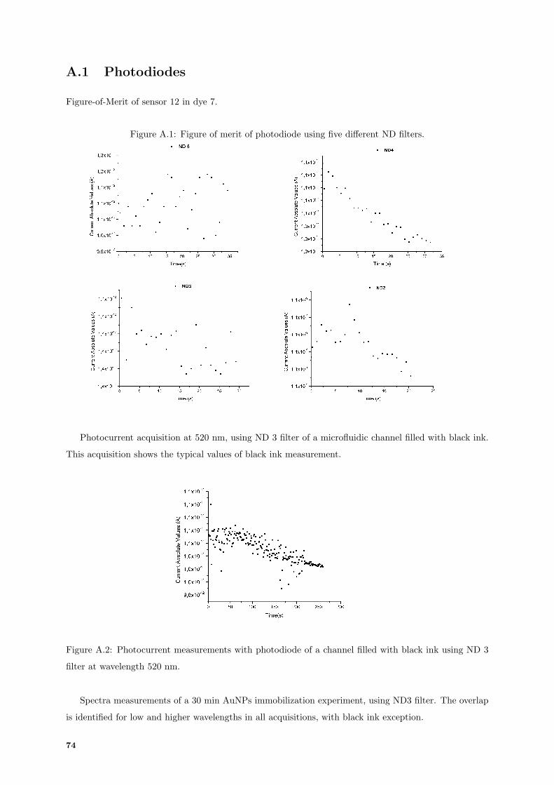
A.1 Photodiodes
Figure-of-Merit of sensor 12 in dye 7.
Figure A.1: Figure of merit of photodiode using five different ND filters.
Photocurrent acquisition at 520 nm, using ND 3 filter of a microfluidic channel filled with black ink.
This acquisition shows the typical values of black ink measurement.
Figure A.2: Photocurrent measurements with photodiode of a channel filled with black ink using ND 3
filter at wavelength 520 nm.
Spectra measurements of a 30 min AuNPs immobilization experiment, using ND3 filter. The overlap
is identified for low and higher wavelengths in all acquisitions, with black ink exception.
74
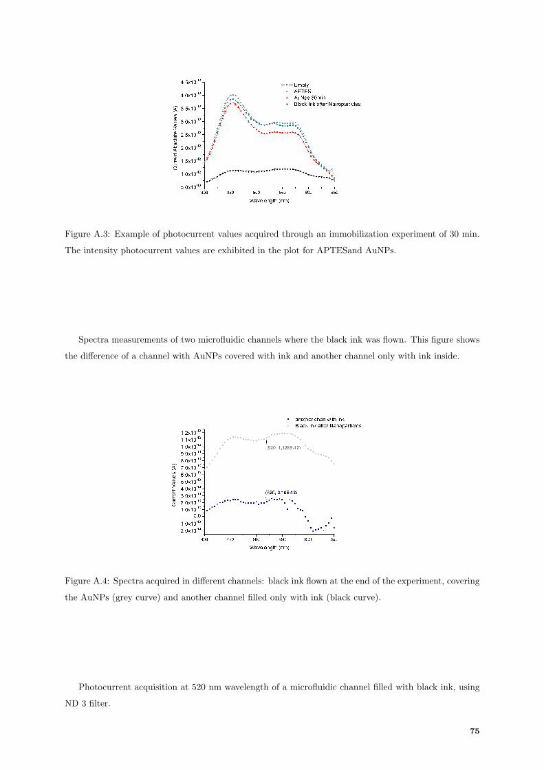
Figure A.3: Example of photocurrent values acquired through an immobilization experiment of 30 min.
The intensity photocurrent values are exhibited in the plot for APTESand AuNPs.
Spectra measurements of two microfluidic channels where the black ink was flown. This figure shows
the difference of a channel with AuNPs covered with ink and another channel only with ink inside.
Figure A.4: Spectra acquired in different channels: black ink flown at the end of the experiment, covering
the AuNPs (grey curve) and another channel filled only with ink (black curve).
Photocurrent acquisition at 520 nm wavelength of a microfluidic channel filled with black ink, using
ND 3 filter.
75
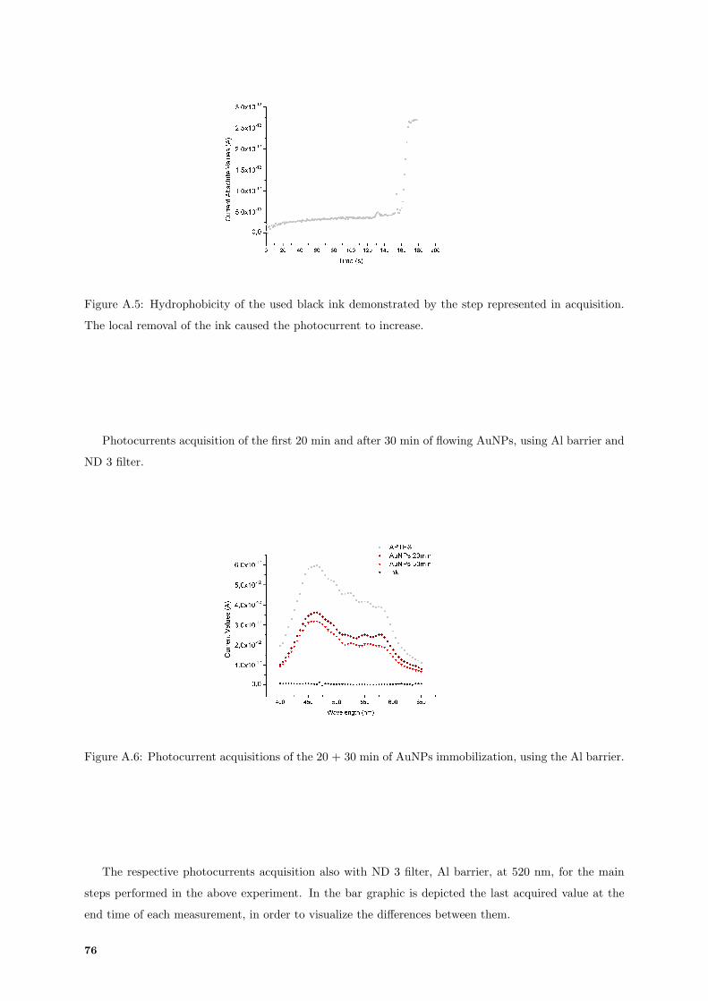
Figure A.5: Hydrophobicity of the used black ink demonstrated by the step represented in acquisition.
The local removal of the ink caused the photocurrent to increase.
Photocurrents acquisition of the first 20 min and after 30 min of flowing AuNPs, using Al barrier and
ND 3 filter.
Figure A.6: Photocurrent acquisitions of the 20 + 30 min of AuNPs immobilization, using the Al barrier.
The respective photocurrents acquisition also with ND 3 filter, Al barrier, at 520 nm, for the main
steps performed in the above experiment. In the bar graphic is depicted the last acquired value at the
end time of each measurement, in order to visualize the differences between them.
76
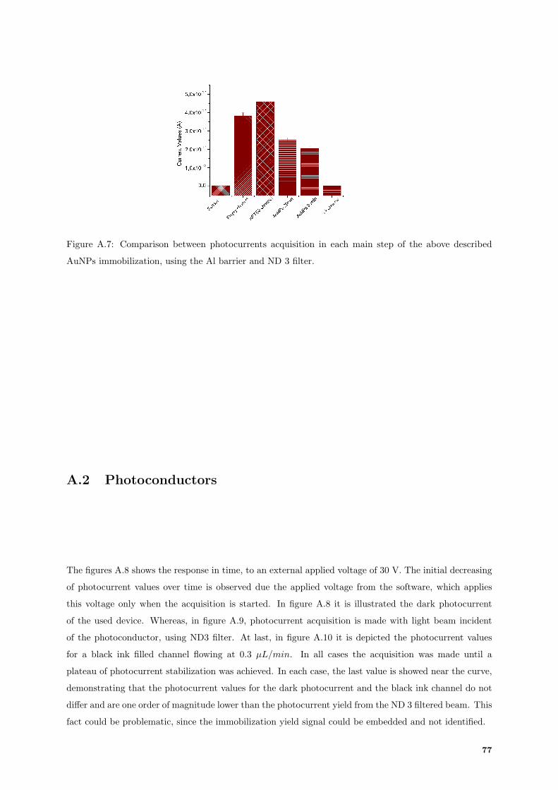
Figure A.7: Comparison between photocurrents acquisition in each main step of the above described
AuNPs immobilization, using the Al barrier and ND 3 filter.
A.2 Photoconductors
The figures A.8 shows the response in time, to an external applied voltage of 30 V. The initial decreasing
of photocurrent values over time is observed due the applied voltage from the software, which applies
this voltage only when the acquisition is started. In figure A.8 it is illustrated the dark photocurrent
of the used device. Whereas, in figure A.9, photocurrent acquisition is made with light beam incident
of the photoconductor, using ND3 filter. At last, in figure A.10 it is depicted the photocurrent values
for a black ink filled channel flowing at 0.3 µL/min. In all cases the acquisition was made until a
plateau of photocurrent stabilization was achieved. In each case, the last value is showed near the curve,
demonstrating that the photocurrent values for the dark photocurrent and the black ink channel do not
differ and are one order of magnitude lower than the photocurrent yield from the ND 3 filtered beam. This
fact could be problematic, since the immobilization yield signal could be embedded and not identified.
77
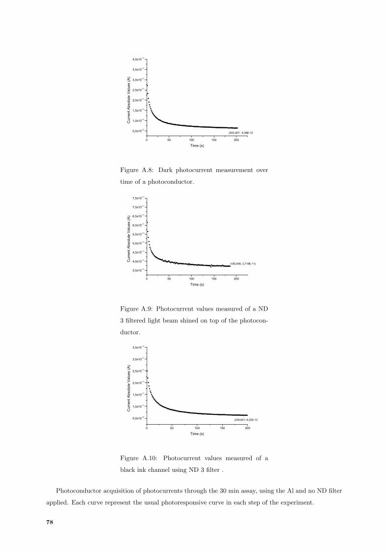
0 50 100 150 200
5,0x10⁻¹²
1,0x10⁻¹¹
1,5x10⁻¹¹
2,0x10⁻¹¹
2,5x10⁻¹¹
3,0x10⁻¹¹
3,5x10⁻¹¹
4,0x10⁻¹¹
Cur
rent
Abs
olut
e V
alue
s (A
)
Time (s)
(202,407; 6,38E-12
Figure A.8: Dark photocurrent measurement over
time of a photoconductor.
0 50 100 150 200
3,5x10⁻¹¹
4,0x10⁻¹¹
4,5x10⁻¹¹
5,0x10⁻¹¹
5,5x10⁻¹¹
6,0x10⁻¹¹
6,5x10⁻¹¹
7,0x10⁻¹¹
7,5x10⁻¹¹
Cur
rent
Abs
olut
e V
alue
s (A
)
Time (s)
(185,906; 3,719E-11)
Figure A.9: Photocurrent values measured of a ND
3 filtered light beam shined on top of the photocon-
ductor.
0 50 100 150 200
5,0x10⁻¹²
1,0x10⁻¹¹
1,5x10⁻¹¹
2,0x10⁻¹¹
2,5x10⁻¹¹
3,0x10⁻¹¹
3,5x10⁻¹¹
Cur
rent
Abs
olut
e V
alue
s (A
)
Time (s)
(200,601; 6,22E-12
Figure A.10: Photocurrent values measured of a
black ink channel using ND 3 filter .
Photoconductor acquisition of photocurrents through the 30 min assay, using the Al and no ND filter
applied. Each curve represent the usual photoresponsive curve in each step of the experiment.
78
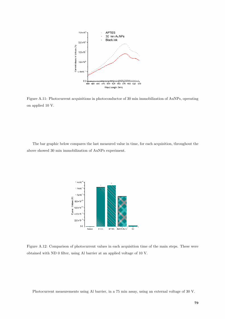
Figure A.11: Photocurrent acquisitions in photoconductor of 30 min immobilization of AuNPs, operating
on applied 10 V.
The bar graphic below compares the last measured value in time, for each acquisition, throughout the
above showed 30 min immobilization of AuNPs experiment.
Figure A.12: Comparison of photocurrent values in each acquisition time of the main steps. These were
obtained with ND 0 filter, using Al barrier at an applied voltage of 10 V.
Photocurrent measurements using Al barrier, in a 75 min assay, using an external voltage of 30 V.
79

Figure A.13: Photocurrents acquired in a 75 min immobilization of AuNPs assay, operatinng on applied
30 V.
The graphic below compares the last measured value in each acquisition, throughout the above 75
min immobilization of AuNPs experiment, using ND 3 filter and the Al barrier.
Figure A.14: Photocurrents acquired in a 75 min immobilization of AuNPs assay, using ND 3 filter, Al
barrier and operating on applied 30 V.
Photocurrent measurements using TiW barrier, ND 3, in a 75 min assay, using an external voltage of
30 V.
80
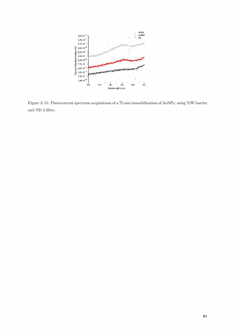
Figure A.15: Photocurrent spectrum acquisitions of a 75 min immobilization of AuNPs, using TiW barrier
and ND 3 filter.
81

A.3 Photodetectors Runsheets
82
Con
stru
ctio
n of
a-S
i:H p
hoto
diod
es b
ased
on
a p-i-n
junc
tion
by P
ECVD
(R
un 0
5)
Den
is S
anto
s –
Dec
embe
r 201
5 C
hip:
Gla
ss [0
.7m
m],
Al [
2000
Å],
n+ a-S
i:H [1
00Å
], i a
-Si:H
[500
0Å],
p+ a-S
i:H [1
00Å
], Si
Nx [
2000
Å],
ITO
[2
000Å
], Ti
W +
Al [
150Å
+ 1
500Å
], Si
Nx [
2000
Å]
1. G
lass
sub
stra
te c
lean
ing
Date:
Substrate:2.5cmx5cmCorning173
7Glass[0
.7m
m]
Machine
:Wetben
ch
Metho
d:Clean
thorou
ghlywith
IPA+Rinsewith
water+Drywith
com
pressedair+
BathinhotAlcon
ox®form
inim
um60min
+Rinsewith
water+Drywith
com
pressedair
VISU
ALIN
SPEC
TIONto
detectresidue
sontheglass
2. B
otto
m e
lect
rode
dep
ositi
on -
Alu
min
um [2
000
Å]
Da
te:
DCm
agne
tron
sputterin
gofAluminum
[200
0Å]
Machine
:Nordiko700
0Dep
osition
con
ditio
ns:Seq
uence“Al200
0Åno
etch”
VISU
ALIN
SPEC
TION
3.
Pho
toresistcoa
t+Electrode
definition
+Develop
men
t
Da
te:
Prog.06/02
–Pho
toresis
tcoa
ting
Machine
:SVG
resis
tcoa
tera
nddevelop
ertrack2
Lasere
xposure
Machine
:Heide
lbergInstrumen
tsDire
ctW
riteLaserLith
ograph
ySystem
(DWL)
Cond
ition
s:Focus:-20
;Ene
rgyfile=85
Map
_AM
SION
Mask:__________L1AlBottomCon
tact____INVE
RTED
___________________________
Maskalignm
ent:(x,y)=
(500
0,50
00)
Prog.06/02
–Pho
toresis
tdevelop
men
tMachine
:SVG
resis
tcoa
tera
nddevelop
ertrack1
MICRO
SCOPE
VISUALIN
SPEC
TIONto
che
ckpho
toresis
tdefinition
4. B
otto
m A
lum
inum
ele
ctro
des
etch
Da
te:
Material:Alum
inum
wetetcha
nt
Machine
:Wetben
ch
Metho
d:Im
merseth
esampleinth
eAlum
inum
etcha
ntand
mon
itoru
ntilun
protectedareas(with
outp
hotoresis
t)
areclean+Washthorou
ghlywith
water+Drywith
com
pressedair.
MICRO
SCOPE
VISUALIN
SPEC
TIONto
verifyetch
83
5. P
hoto
resi
st s
trip
D
ate:
Material:Microstrip
Machine
:Wetben
ch
Metho
d:Im
merseth
esampleinhotm
icrostrip
for5
-10min.+Rinsewith
IPA+Rinsewith
water+Drywith
compressedair.
MICRO
SCOPE
VISUALIN
SPEC
TIONto
verifycom
pleteph
otoresistre
moval
6. n-i-p
a-Si
:H d
epos
ition
[10
0Å, 5
000Å
,100
Å]
Date:
Mac
hine
: rf-P
EC
VD
6.1
n+ a-S
i:H [1
00Å
] dep
ositi
on b
y R
F
Cond
ition
s:V=0V,T
subs=250
ºC,P=0.1Torr,P R
F=5W
,F(SiH
4)=10sccm
,F(P
H 3/H
2)=5sc
cm
Dep
osition
time:1m
in40s(1.37
Å/s)
6.2
i a-S
i:H [5
000Å
] dep
ositi
on b
y R
F
Cond
ition
s:V=0V,T
subs=25
0ºC,P=0.1Torr,P R
F=5W
,F(SiH
4)=10sccm
Dep
osition
rate:D
eposition
time:1h00min50s(1.37
Å/s)
6.3
p+ a-S
i:H [1
00Å
] dep
ositi
on b
y R
F
Cond
ition
s:V=0V,T
subs=250
ºC,P=0.1Torr,P R
F=5W
,F(SiH
4)=10sccm
,F(B
2H6/H 2)=
5sc
cm
Dep
osition
time:1m
in40s(1.37
Å/s)
VISU
ALIN
SPEC
TION
7. R
esis
t coa
t and
isla
nd d
efin
ition
Da
te:
Prog.06/02
–Pho
toresis
tcoa
ting
Machine
:SVG
resis
tcoa
tera
nddevelop
ertrack2
Lasere
xposure
Machine
:Heide
lbergInstrumen
tsDire
ctW
riteLaserLith
ograph
ySystem
(DWL)
Cond
ition
s:Focus:-20
;Ene
rgyfile=85
Map
_AM
SION
Mask:__________L2n-i-paSiH____INVE
RTED
___________________________
Maskalignm
ent:(x,y)=
(70,70
) Prog.06/02
–Pho
toresis
tdevelop
men
tMachine
:SVG
resis
tcoa
tera
nddevelop
ertrack1
MICRO
SCOPE
VISUALIN
SPEC
TIONto
che
ckpho
toresis
tdefinition
8. n-i-p
isla
nd e
tch
via
RIE
usi
ng L
AM
D
ate:
Reactiv
eIonEtching(RIE)o
fthe
n-i-pa-Si:Hisland
sMachine
:LAM
ResearchRa
inbo
wPlasm
aEtcher
Cond
ition
s:RecipeSF6_
CHF3;P=100
mTo
rr;P=200
W;F(SF 6)=
50sccm
;F(CHF
3)=50sccm
Etchingtim
e=20
0s
MICRO
SCOPE
VISUALIN
SPEC
TIONto
n-i-pislan
dchecketch
84
9. P
hoto
resi
st s
trip
D
ate:
Material:Microstrip
Machine
:Wetben
ch
Metho
d:Im
merseth
esampleinhotm
icrostrip
for1
5min.+Rinsewith
IPA+Rinsewith
water+Drywith
compressedair.
MICRO
SCOPE
VISUALIN
SPEC
TIONto
verifycom
pleteph
otoresistre
moval
10. R
esis
t coa
t for
SiN
x vi
a de
finiti
on
Dat
e:
Prog.06/02
–Pho
toresis
tcoa
ting
Machine
:SVG
resis
tcoa
tera
nddevelop
ertrack2
Lasere
xposure
Machine
:Heide
lbergInstrumen
tsDire
ctW
riteLaserLith
ograph
ySystem
(DWL)
Cond
ition
s:Focus:-20
;Ene
rgyfile=85
Map
_AM
SION
Mask:__________L3aSiHvia____INVE
RTED
___________________________
Maskalignm
ent:(x,y)=
(70,70
) Prog.06/02
–Pho
toresis
tdevelop
men
tMachine
:SVG
resis
tcoa
tera
nddevelop
ertrack1
MICRO
SCOPE
VISUALIN
SPEC
TIONto
che
ckpho
toresis
tdefinition
11. S
iNx
late
ral w
all p
assi
vatio
n la
yer d
epos
ition
SiNx[200
0Å]
D
ate:
RF-PEC
VDdep
osition
ofSiNx[200
0Å]
Machine
:RF-PE
CVD
Cond
ition
s:V=0V;T
sub=
100
o C;P=10
0mTo
rr;P R
F=10W;F(SiH4)=5sc
cm;F(NH 3)=
10sccm
;F(H2)=35sccm
Dep
osition
time:1h30min
VISU
ALIN
SPEC
TION
12. S
iNx
via
and
pads
lift-
off
D
ate:
Material:Microstrip
Machine
:Wetben
ch
Metho
d:Im
merseth
esampleinhotm
icrostrip
(occasiona
lultrason
icpulses)+rinsewith
water+drywith
compressedair,checkthelift-offp
rocessinth
emicroscop
ean
drepe
atth
estep
sabo
veifincomplete.
MICRO
SCOPE
VISUALIN
SPEC
TIONto
che
ckfo
rclean
lift-off
13. R
esis
t coa
t for
ITO
top
cont
act d
efin
ition
Dat
e:
Prog.06/02
–Pho
toresis
tcoa
ting
Machine
:SVG
resis
tcoa
tera
nddevelop
ertrack2
Lasere
xposure
Machine
:Heide
lbergInstrumen
tsDire
ctW
riteLaserLith
ograph
ySystem
(DWL)
Cond
ition
s:Focus:-20
;Ene
rgyfile=85
Map
_AM
SION
Mask:__________L4ITOTop
Con
tact____N
ON_INVE
RTED
___________________________
Maskalignm
ent:(x,y)=
(70,70
) Prog.06/02
–Pho
toresis
tdevelop
men
tMachine
:SVG
resis
tcoa
tera
nddevelop
ertrack1
MICRO
SCOPE
VISUALIN
SPEC
TIONto
che
ckpho
toresis
tdefinition
85
14. I
TO to
p co
ntac
t dep
ositi
on IT
O [2
000Å
]
Dat
e:
DCM
agne
tron
Spu
tteringofITO[2
000Å]
Machine
:Alcatel
Cond
ition
s:
Depo
sitiontim
e:
Calibratio
nsample:_______________________________
VISU
ALIN
SPEC
TION
15. I
TO to
p co
ntac
t lift
-off
D
ate:
Material:Microstrip
Machine
:Wetben
ch
Metho
d:Im
merseth
esampleinhotm
icrostrip
(occasiona
lultrason
icpulses)+rinsewith
water+drywith
compressedair,checkthelift-offp
rocessinth
emicroscop
ean
drepe
atth
estep
sabo
veifincomplete.
MICRO
SCOPE
VISUALIN
SPEC
TIONto
che
ckfo
rclean
lift-off
16. R
esis
t coa
t for
met
allic
top
lines
def
initi
on
D
ate:
Prog.06/02
–Pho
toresis
tcoa
ting
Machine
:SVG
resis
tcoa
tera
nddevelop
ertrack2
Lasere
xposure
Machine
:Heide
lbergInstrumen
tsDire
ctW
riteLaserLith
ograph
ySystem
(DWL)
Cond
ition
s:Focus:-20
;Ene
rgyfile=85
Map
_AM
SION
Mask:__________L5AlTop
Con
tact____N
ON_INVE
RTED
___________________________
Maskalignm
ent:(x,y)=
(70,70
) Prog.06/02
–Pho
toresis
tdevelop
men
tMachine
:SVG
resis
tcoa
tera
nddevelop
ertrack1
MICRO
SCOPE
VISUALIN
SPEC
TIONto
che
ckpho
toresis
tdefinition
17. M
etal
lic to
p lin
es d
epos
ition
TiW
[150
Å] +
Al [
1500
Å]
Dat
e:
Magne
tron
sputterin
gofTita
nium
Tun
gsten[150
Å]and
Aluminum
[150
0Å]
Machine
:Nordiko700
0Dep
osition
con
ditio
ns:
VISU
ALIN
SPEC
TION
18. M
etal
lic to
p lin
es li
ft-of
f
Dat
e:
Material:Microstrip
Machine
:Wetben
ch
Metho
d:Im
merseth
esampleinhotm
icrostrip
(occasiona
lultrason
icpulses)+rinsewith
water+drywith
compressedair,checkthelift-offp
rocessinth
emicroscop
ean
drepe
atth
estep
sabo
veifincomplete.
MICRO
SCOPE
VISUALIN
SPEC
TIONto
che
ckfo
rclean
lift-off
86
19. P
rote
ctiv
e la
yer a
nd p
ad d
efin
ition
D
ate:
Prog.06/02
–Pho
toresis
tcoa
ting
Machine
:SVG
resis
tcoa
tera
nddevelop
ertrack2
Lasere
xposure
Machine
:Heide
lbergInstrumen
tsDire
ctW
riteLaserLith
ograph
ySystem
(DWL)
Cond
ition
s:Focus:-20
;Ene
rgyfile=85
Map
_AM
SION
Mask:__________L6SiNxVia____INVE
RTED
___________________________
Maskalignm
ent:(x,y)=
(70,70
) Prog.06/02
–Pho
toresis
tdevelop
men
tMachine
:SVG
resis
tcoa
tera
nddevelop
ertrack1
MICRO
SCOPE
VISUALIN
SPEC
TIONto
che
ckpho
toresis
tdefinition
20. P
rote
ctiv
e la
yer d
epos
ition
SiN
x [2
000Å
]
Dat
e:
RF-PEC
VDdep
osition
ofSiNx[200
0Å]
Machine
:RF-PE
CVD
Cond
ition
s:V=0V;T
sub=
100
o C;P=10
0mTo
rr;P R
F=10W;F(SiH4)=5sc
cm;F(NH 3)=
10sccm
;F(H2)=35sccm
Dep
osition
time:1h30min
VISU
ALIN
SPEC
TION
21. P
rote
ctiv
e la
yer l
ift-o
ff.
D
ate:
Material:Microstrip
Machine
:Wetben
ch
Metho
d:Im
merseth
esampleinhotm
icrostrip
(occasiona
lultrason
icpulses)+rinsewith
water+drywith
compressedair,checkthelift-offp
rocessinth
emicroscop
ean
drepe
atth
estep
sabo
veifincomplete.
MICRO
SCOPE
VISUALIN
SPEC
TIONto
che
ckfo
rclean
lift-off
22. P
hoto
resi
st c
oatin
g fo
r cut
ting
Dat
e:
Prog.06/02
–Pho
toresis
tcoa
ting
Machine
:SVG
resis
tcoa
tera
nddevelop
ertrack2
23. D
icin
g sa
mpl
es in
indi
vidu
als
dies
D
ate:
Machine
:Disc
oDA
D32
1DicingSaw
24. P
hoto
resi
st s
trip
D
ate:
Material:Microstrip
Machine
:Wetben
ch
Metho
d:Im
merseth
esampleinhotm
icrostrip
for1
5min.+Rinsewith
IPA+Rinsewith
water+Drywith
compressedair.
87
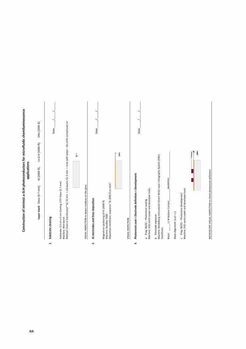
Constructio
nofintrinsica-Si:Hpho
tocond
uctorsfo
rmicroflu
idicche
milu
minescence
applications
Layerstack:Glass[0
.7m
m];Al[2
000Å],ia-Si:H
[500
0Å];SiNx[200
0Å]
1.
Su
bstratecleaning
Da
te_____/_____/______
Substrate:2.5cmx5cmCorning173
7Glass[0
.7m
m]
Machine
:Wetben
ch
Metho
d:Clean
inhotAlcon
ox®for2
5min.+ultrason
icfo
r5m
in.+rinsewith
water+drywith
com
pressedair
VISU
ALIN
SPEC
TIONto
detectresidue
sontheglass
2.
Alelectrode
san
dlin
esdep
osition
Da
te_____/_____/______
Magne
tron
sputterin
gofAl[20
00Å]
Machine
:Nordiko700
0De
positioncond
ition
s:se
quen
ce“Al200
0Åno
etch”
VISU
ALIN
SPEC
TION
3.
Ph
otoresistcoa
t+Electrode
definition
+Develop
men
tDa
te_____/_____/______
a. Prog.06/02
–Pho
toresis
tcoa
ting
Machine
:SVG
resis
tcoa
tera
nddevelop
ertrack
b. Electrod
eexpo
sure
Machine
:Heide
lbergInstrumen
tsDire
ctW
riteLaserLith
ograph
ySystem
(DWL)
Cond
ition
s:
Mask:_____L
1AlBottomCon
tact_________INVE
RTED
____________________
Maskalignm
ent:(x,y)=
(,)
c. Prog.06/02
–Pho
toresis
tdevelop
men
tMachine
:SVG
resis
tcoa
tera
nddevelop
ertrack
MICRO
SCOPE
VISUALIN
SPEC
TIONto
che
ckpho
toresis
tdefinition
APP
END
IX I
II: R
UN
SH
EETS
USE
D I
N T
HE
MIC
ROFA
BRIC
ATI
ON
OF
THE
AM
ORP
HO
US
SILI
CON
PH
OTO
SEN
SORS
17
3
III.
2.
Run
shee
t PP
Th
e pr
esen
t run
she
et d
escr
ibes
the
mic
rofa
bric
atio
n pr
oces
sing
of th
e in
tegr
ated
amor
phou
s sili
con
phot
ocon
duct
or fo
r flu
ores
cenc
e det
ectio
n.
R
espo
nsib
le: A
lexa
ndra
Pim
ente
l
Dat
e: _
_Set
embr
o 20
07
Des
crip
tion:
Stu
dy o
f the
fluo
resc
ence
resp
onse
of a
par
alle
l con
tact
a-S
i:H (5
000
Å) d
evic
e w
ith a
-
SiC:
H (1
.96µ
m) f
luor
esce
nce
filte
r.
Al e
lect
rode
s are
dep
osite
d ov
er g
lass
subs
trate
and
a-S
i:H is
land
s are
def
ined
ove
r the
ele
ctro
des.
Laye
r st
ack:
Gla
ss (1
mm
) / A
l (15
00 Ǻ
) / i
a-Si
:H (5
000 Ǻ)
/ a-
SiC:
H (1
.96 µm
) / S
iO2 (7
50 Ǻ
).
Step
2: E
lect
rode
s Dep
ositi
on
Subs
trate
: gla
ss
Mac
hine
: Nor
diko
700
0 D
epos
ition
con
ditio
ns b
y Sp
utte
ring
of A
l:
P=1k
W ;
F Ar =
50
sccm
; P =
3 m
Torr
mod
4 / f
30 /
Seq.
69; t
=___
_s
Al t
arge
t thi
ckne
ss =
150
0 Å
Dat
e: _
_/07
/200
6
Re
spon
sible
: A. P
imen
tel
Dat
e: _
_/07
/200
6
Re
spon
sible
: A. P
imen
tel
Step
1: S
ubstr
ate
Clea
ning
Su
bstra
te: 2
.5 c
m x
5cm
Cor
ning
705
9 gl
ass
Mac
hine
: wet
ben
ch
Cond
ition
s: Cl
ean
in
hot
Alc
anox
du
ring
25
min
.; ul
traso
nic f
or 5
min
; rin
se w
ith w
ater
: dry
com
pres
sed
air
APP
END
IX I
II: R
UN
SH
EETS
USE
D I
N T
HE
MIC
ROFA
BRI
CA
TIO
N O
F TH
E A
MO
RPH
OU
S SI
LIC
ON
PH
OTO
SEN
SORS
17
3
III.
2.
Run
shee
t PP
Th
e pr
esen
t run
she
et d
escr
ibes
the
mic
rofa
bric
atio
n pr
oces
sing
of th
e in
tegr
ated
amor
phou
s sili
con
phot
ocon
duct
or fo
r flu
ores
cenc
e de
tect
ion.
R
espo
nsib
le: A
lexa
ndra
Pim
ente
l
Dat
e: _
_Set
embr
o 20
07
Des
crip
tion:
Stu
dy o
f the
fluo
resc
ence
resp
onse
of a
par
alle
l con
tact
a-S
i:H (5
000
Å) d
evic
e w
ith a
-
SiC:
H (1
.96µ
m) f
luor
esce
nce
filte
r.
Al e
lect
rode
s are
dep
osite
d ov
er g
lass
subs
trate
and
a-S
i:H is
land
s are
def
ined
ove
r the
ele
ctro
des.
Laye
r st
ack:
Gla
ss (1
mm
) / A
l (15
00 Ǻ
) / i
a-Si
:H (5
000 Ǻ)
/ a-
SiC:
H (1
.96 µm
) / S
iO2 (7
50 Ǻ
).
Step
2: E
lect
rode
s Dep
ositi
on
Subs
trate
: gla
ss
Mac
hine
: Nor
diko
700
0 D
epos
ition
con
ditio
ns b
y Sp
utte
ring
of A
l:
P=1k
W ;
F Ar =
50
sccm
; P =
3 m
Torr
mod
4 / f
30 /
Seq.
69; t
=___
_s
Al t
arge
t thi
ckne
ss =
150
0 Å
Dat
e: _
_/07
/200
6
Re
spon
sible
: A. P
imen
tel
Dat
e: _
_/07
/200
6
Re
spon
sible
: A. P
imen
tel
Step
1: S
ubst
rate
Cle
anin
g Su
bstra
te: 2
.5 c
m x
5cm
Cor
ning
705
9 gl
ass
Mac
hine
: wet
ben
ch
Cond
ition
s: Cl
ean
in
hot
Alc
anox
du
ring
25
min
.; ul
traso
nic
for 5
min
; rin
se w
ith w
ater
: dry
com
pres
sed
air
APP
END
IX II
I:RU
N S
HEE
TS U
SED
IN T
HE
MIC
ROFA
BRIC
ATI
ON
OF
THE
AM
ORP
HO
US
SILI
CON
PH
OTO
SEN
SORS
174
Dat
e: _
_/07
/200
6
Re
spon
sible
: A. P
imen
tel
Step
5: P
hoto
resis
t Stri
p M
achi
ne: w
et b
ench
Su
bstra
te: g
lass
/ Al/
PR
Cond
ition
s for
Pho
tore
sist S
tripp
ing:
ho
t m
icro
strip
for
20
min
; IP
A r
inse
; D
I rin
se;
dry
com
pres
sed
air
Dat
e: _
_/07
/200
6
Re
spon
sible
: A. P
imen
tel
Step
4: E
lect
rode
s Wet
Etc
hing
Su
bstra
te: g
lass
/ Al/
PR
Mac
hine
: w
et b
ench
Co
nditi
ons f
or A
l Wet
Etc
hing
: Al E
tcha
nt
Thic
knes
s to
rem
ove:
150
0 Å
Etc
h ra
te: 1
1 Å
/s.
Ove
retc
h : u
ntil
glas
s is c
lean
. Te
mpe
ratu
re: @
RT
Dat
e: _
_/07
/200
6
R
espo
nsib
le: V
. Soa
res a
nd A
.Pim
ente
l
Step
3: P
hoto
resis
t Coa
t + B
otto
m E
lect
rode
Exp
osur
e (A
l) +
Dev
elop
men
t
3.1.
Pho
tore
sist C
oat
Mac
hine
: SV
G tr
ack
Subs
trate
: gla
ss/ A
l Ph
otor
esist
Coa
ting
cond
ition
s: 1)
Pro
g 03
/02,
SV
G h
ot p
late
(pre
treat
men
t: 60
s pre
-hea
t @ 1
10ºC
) 2)
Pro
g 06
/02,
Targ
et th
ickn
ess:
1200
nm
3.2.
Ele
ctro
des E
xpos
ure
Subs
trate
: gla
ss/A
l(150
0 Ǻ
) M
achi
ne: D
WL
Mas
k: p
palin
v
Map
: PP
Alig
nmen
t mar
k ap
pear
ing
on th
is la
yer:
(x,y
)=(1
68,5
4)
Ener
gy: _
____
_ ;
L
aser
Pow
er: _
____
_ ;
Foc
us: _
____
__
3.3.
Dev
elop
D
evel
opm
ent c
ondi
tions
: Pr
og.
05/0
2 -
pre-
heat
at
100
ºC d
urin
g 60
s +
60
s de
velo
p.
88
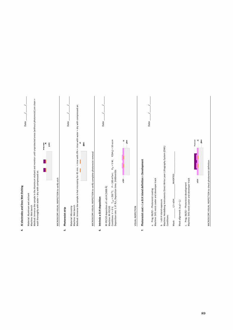
4.
Alelectrode
san
dlin
esW
etEtching
Da
te_____/_____/______
Material:Alum
inum
wetetcha
nt
Machine
:Wetben
ch
Metho
d:Im
merseth
esampleinth
eAlum
inum
etcha
ntand
mon
itoru
ntilun
protectedareas(with
outp
hotoresis
t)areclean
+
washthorou
ghlywith
water+drywith
com
pressedair.
MICRO
SCOPE
VISUALIN
SPEC
TIONto
verifyetch
5.
Ph
otoresiststrip
Date_____/_____/______
Material:Microstrip
Machine
:Wetben
ch
Metho
d:Im
merseth
esampleinhotm
icrostrip
for4
5min.+rinsewith
IPA+rin
sewith
water+drywith
com
pressedair.
MICRO
SCOPE
VISUALIN
SPEC
TIONto
verifycom
pleteph
otoresistre
moval
6.
Intrinsica-Si:Hdep
osition
Da
te_____/_____/______
RF-PEC
VDdep
osition
ofi-aSi:H[5
000Å]
Machine
:RF-PE
CVD
Cond
ition
s:V=0V;T s
ub=250
o C;P=10
0mTo
rr;P R
F=5W
;F(SiH4)=10sccm
De
positionrate:1
.37Å/s,Dep
osition
time:1h0
0min50
s
VISU
ALIN
SPEC
TION
7.
Ph
otoresistcoa
t+ia-Si:Hisland
definition
+Develop
men
t
Date_____/_____/______
a. Prog.06/02
–Pho
toresis
tcoa
ting
Machine
:SVG
resis
tcoa
tera
nddevelop
ertrack
b. i-a
Si:Hisland
exposure
Machine
:Heide
lbergInstrumen
tsDire
ctW
riteLaserLith
ograph
ySystem
(DWL)
Cond
ition
s:
Mask:________L2
i-aSiH____________INVE
RTED
__________________
Maskalignm
ent:(x,y)=
(,)
c. Prog.06/02
–Pho
toresis
tdevelop
men
tMachine
:SVG
resis
tcoa
tera
nddevelop
ertrack
MICRO
SCOPE
VISUALIN
SPEC
TIONto
che
ckpho
toresis
tdefinition
APP
END
IX II
I:RU
N S
HEE
TS U
SED
IN T
HE
MIC
ROFA
BRI
CA
TIO
N O
F TH
E A
MO
RPH
OU
S SI
LIC
ON
PH
OTO
SEN
SORS
174
Dat
e: _
_/07
/200
6
Re
spon
sible
: A. P
imen
tel
Step
5: P
hoto
resi
st S
trip
M
achi
ne: w
et b
ench
Su
bstra
te: g
lass
/ Al/
PR
Cond
ition
s for
Pho
tore
sist S
tripp
ing:
ho
t m
icro
strip
for
20
min
; IP
A r
inse
; D
I rin
se;
dry
com
pres
sed
air
Dat
e: _
_/07
/200
6
Re
spon
sible
: A. P
imen
tel
Step
4: E
lect
rode
s Wet
Etc
hing
Su
bstra
te: g
lass
/ Al/
PR
Mac
hine
: w
et b
ench
Co
nditi
ons f
or A
l Wet
Etc
hing
: Al E
tcha
nt
Thic
knes
s to
rem
ove:
150
0 Å
Etc
h ra
te: 1
1 Å
/s.
Ove
retc
h : u
ntil
glas
s is c
lean
. Te
mpe
ratu
re: @
RT
Dat
e: _
_/07
/200
6
R
espo
nsib
le: V
. Soa
res a
nd A
.Pim
ente
l
Step
3: P
hoto
resi
st C
oat +
Bot
tom
Ele
ctro
de E
xpos
ure
(Al)
+ D
evel
opm
ent
3.1.
Pho
tore
sist
Coa
t M
achi
ne :
SVG
trac
k Su
bstra
te: g
lass
/ Al
Phot
ores
ist C
oatin
g co
nditi
ons:
1)
Pro
g 03
/02,
SV
G h
ot p
late
(pre
treat
men
t: 60
s pre
-hea
t @ 1
10ºC
) 2)
Pro
g 06
/02,
Targ
et th
ickn
ess:
1200
nm
3.2.
Ele
ctro
des E
xpos
ure
Subs
trate
: gla
ss/A
l(150
0 Ǻ
) M
achi
ne: D
WL
Mas
k: p
palin
v
Map
: PP
Alig
nmen
t mar
k ap
pear
ing
on th
is la
yer:
(x,y
)=(1
68,5
4)
Ener
gy: _
____
_ ;
L
aser
Pow
er: _
____
_ ;
Foc
us: _
____
__
3.3.
Dev
elop
D
evel
opm
ent c
ondi
tions
: Pr
og.
05/0
2 -
pre-
heat
at
100
ºC d
urin
g 60
s +
60
s de
velo
p.
APP
END
IX II
I:RU
N S
HEE
TS U
SED
IN T
HE
MIC
ROFA
BRI
CA
TIO
N O
F TH
E A
MO
RPH
OU
S SI
LIC
ON
PH
OTO
SEN
SORS
174
Dat
e: _
_/07
/200
6
Re
spon
sible
: A. P
imen
tel
Step
5: P
hoto
resi
st S
trip
M
achi
ne: w
et b
ench
Su
bstra
te: g
lass
/ Al/
PR
Cond
ition
s for
Pho
tore
sist S
tripp
ing:
ho
t m
icro
strip
for
20
min
; IP
A r
inse
; D
I rin
se;
dry
com
pres
sed
air
Dat
e: _
_/07
/200
6
Re
spon
sible
: A. P
imen
tel
Step
4: E
lect
rode
s Wet
Etc
hing
Su
bstra
te: g
lass
/ Al/
PR
Mac
hine
: w
et b
ench
Co
nditi
ons f
or A
l Wet
Etc
hing
: Al E
tcha
nt
Thic
knes
s to
rem
ove:
150
0 Å
Etc
h ra
te: 1
1 Å
/s.
Ove
retc
h : u
ntil
glas
s is c
lean
. Te
mpe
ratu
re: @
RT
Dat
e: _
_/07
/200
6
R
espo
nsib
le: V
. Soa
res a
nd A
.Pim
ente
l
Step
3: P
hoto
resi
st C
oat +
Bot
tom
Ele
ctro
de E
xpos
ure
(Al)
+ D
evel
opm
ent
3.1.
Pho
tore
sist
Coa
t M
achi
ne :
SVG
trac
k Su
bstra
te: g
lass
/ Al
Phot
ores
ist C
oatin
g co
nditi
ons:
1)
Pro
g 03
/02,
SV
G h
ot p
late
(pre
treat
men
t: 60
s pre
-hea
t @ 1
10ºC
) 2)
Pro
g 06
/02,
Targ
et th
ickn
ess:
1200
nm
3.2.
Ele
ctro
des E
xpos
ure
Subs
trate
: gla
ss/A
l(150
0 Ǻ
) M
achi
ne: D
WL
Mas
k: p
palin
v
Map
: PP
Alig
nmen
t mar
k ap
pear
ing
on th
is la
yer:
(x,y
)=(1
68,5
4)
Ener
gy: _
____
_ ;
L
aser
Pow
er: _
____
_ ;
Foc
us: _
____
__
3.3.
Dev
elop
D
evel
opm
ent c
ondi
tions
: Pr
og.
05/0
2 -
pre-
heat
at
100
ºC d
urin
g 60
s +
60
s de
velo
p. A
PPEN
DIX
III
: RU
N S
HEE
TS U
SED
IN
TH
E M
ICR
OFA
BR
ICA
TIO
N O
F TH
E A
MO
RPH
OU
S SI
LIC
ON
PH
OTO
SEN
SORS
17
5
Step
8: i
a-S
i:H Is
land
RIE
Su
bstra
te: g
lass
/ Al /
i a-
Si:H
/ PR
M
achi
ne: L
AM
R
eact
ive
Ion
Etch
ing
(RIE
) con
ditio
ns:
Rec
ipe
6 Th
ickn
ess t
o re
mov
e: ~
5000
Å
Etch
rate
of i
a-S
i:H: 1
5.3
Å/s
Et
ch ti
me:
___
_ s+
100%
Ove
rEtc
h
Act
ual e
tch
time:
Ove
retc
h un
til g
lass
is c
lean
.
Dat
e: _
_/07
/200
6
R
espo
nsib
le: V
. Soa
res a
nd A
. Pim
ente
l
Dat
e: _
_/07
/200
6
R
espo
nsib
le: V
. Soa
res a
nd A
. Pim
ente
l
Step
7: P
hoto
resi
st C
oat +
i a-
Si:H
Isla
nd E
xpos
ure
+ D
evel
opm
ent
7.1.
Pho
tore
sist
Coa
t: R
epea
t ste
p 3.
1.
7.2:
i a-
Si:H
Isla
nd E
xpos
ure
Subs
trate
: gla
ss/ A
l/ i a
-Si:H
/ PR
Mac
hine
: DW
L M
ask:
ppi
slin
v M
ap: P
P A
lignm
ent m
ark
appe
arin
g on
this
laye
r: (x
,y)=
(168
,174
) Ex
posu
re C
ondi
tions
: En
ergy
: __
La
ser P
ower
: ___
mW
Fo
cus:
__
Offs
ets:
X=_
__
Y
=___
sc
. __
7.3.
Dev
elop
: Rep
eat s
tep
3.3
Step
6: P
EC
VD
Dep
ositi
on o
f i a
-Si:H
Dat
e: _
_/07
/200
6
Res
pons
ible
: J.P
. Con
de a
nd A
. Pim
ente
l
Subs
trate
: gla
ss/ A
l/ M
achi
ne: R
F-U
HV
C
ondi
tions
for i
a-S
i:H (5
000 Ǻ
) PEC
VD
dep
ositi
on:
V=
0 V
T Sub
= 2
50 ºC
P=
0.1
Tor
r P R
F =
5 W
F S
iH4 =
10
sccm
d tar
get:
5000
Å
r dep
ositi
on:
0.73
Å/s
D
epos
ition
Tim
e: 1
h00m
in50
s St
art @
___
h___
min
Fi
nish
@ _
__h_
__m
in
APP
END
IX I
II: R
UN
SH
EETS
USE
D I
N T
HE
MIC
ROFA
BRIC
ATI
ON
OF
THE
AM
ORP
HO
US
SILI
CON
PH
OTO
SEN
SORS
17
5
Step
8: i
a-S
i:H Is
land
RIE
Su
bstra
te: g
lass
/ Al /
i a-
Si:H
/ PR
M
achi
ne: L
AM
Re
activ
e Io
n Et
chin
g (R
IE) c
ondi
tions
: Re
cipe
6
Thic
knes
s to
rem
ove:
~50
00 Å
Et
ch ra
te o
f i a
-Si:H
: 15.
3 Å
/s
Etch
tim
e: _
___
s+10
0% O
verE
tch
A
ctua
l etc
h tim
e: O
vere
tch
until
gla
ss is
cle
an.
Dat
e: _
_/07
/200
6
R
espo
nsib
le: V
. Soa
res a
nd A
. Pim
ente
l
Dat
e: _
_/07
/200
6
R
espo
nsib
le: V
. Soa
res a
nd A
. Pim
ente
l
Step
7: P
hoto
resi
st C
oat +
i a-
Si:H
Isla
nd E
xpos
ure
+ D
evel
opm
ent
7.1.
Pho
tore
sist C
oat:
Repe
at st
ep 3
.1.
7.2:
i a-
Si:H
Isla
nd E
xpos
ure
Subs
trate
: gla
ss/ A
l/ i a
-Si:H
/ PR
Mac
hine
: DW
L M
ask:
ppi
slinv
M
ap: P
P A
lignm
ent m
ark
appe
arin
g on
this
laye
r: (x
,y)=
(168
,174
) Ex
posu
re C
ondi
tions
: En
ergy
: __
La
ser P
ower
: ___
mW
Fo
cus:
__
Offs
ets:
X=_
__
Y
=___
sc
. __
7.3.
Dev
elop
: Rep
eat s
tep
3.3
Step
6: P
ECVD
Dep
ositi
on o
f i a
-Si:H
Dat
e: _
_/07
/200
6
Res
pons
ible
: J.P
. Con
de a
nd A
. Pim
ente
l
Subs
trate
: gla
ss/ A
l/ M
achi
ne: R
F-U
HV
Co
nditi
ons f
or i
a-Si
:H (5
000 Ǻ
) PEC
VD
dep
ositi
on:
V=
0 V
T Sub
= 2
50 ºC
P=
0.1
Tor
r P R
F =
5 W
F S
iH4 =
10
sccm
d tar
get:
5000
Å
r depo
sitio
n: 0
.73
Å/s
Dep
ositi
on T
ime:
1h0
0min
50s
Star
t @ _
__h_
__m
in
Fini
sh @
___
h___
min
89
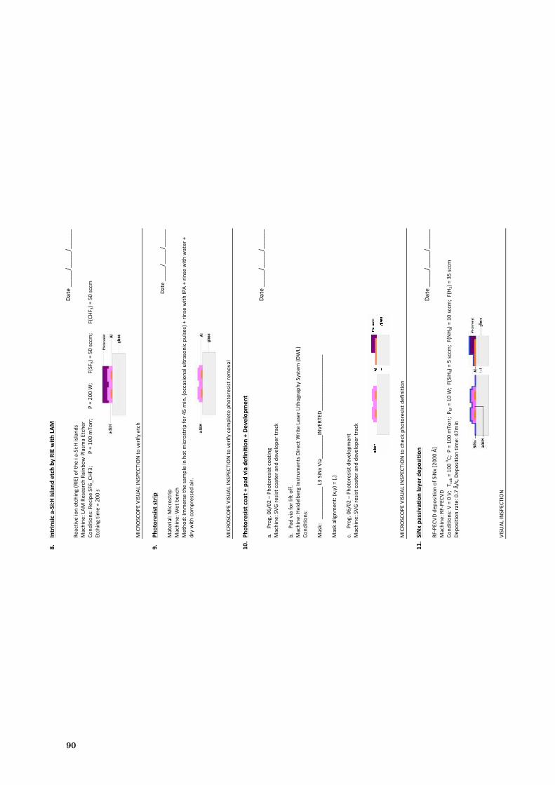
8.
Intrinsica-Si:Hisland
etchby
RIEwith
LAM
Date_____/_____/______
Reactiv
eionetching(RIE)o
fthe
ia-Si:Hisland
sMachine
:LAM
ResearchRa
inbo
wPlasm
aEtcher
Cond
ition
s:RecipeSF6_
CHF3;P=100
mTo
rr;P=200
W;F(SF 6)=
50sccm
;F(CHF
3)=50sccm
Etchingtim
e=20
0s
MICRO
SCOPE
VISUALIN
SPEC
TIONto
verifyetch
9.
Ph
otoresiststrip
Date_____/_____/______
Material:Microstrip
Machine
:Wetben
ch
Metho
d:Im
merseth
esampleinhotm
icrostrip
for4
5min.(occasio
nalultrason
icpulses)+rinsewith
IPA+rin
sewith
water+
drywith
com
pressedair.
MICRO
SCOPE
VISUALIN
SPEC
TIONto
verifycom
pleteph
otoresistre
moval
10
. Ph
otoresistcoa
t+pad
viadefinition
+Develop
men
t
Date_____/_____/______
a. Prog.06/02
–Pho
toresis
tcoa
ting
Machine
:SVG
resis
tcoa
tera
nddevelop
ertrack
b. Padviaforliftoff.
Machine
:Heide
lbergInstrumen
tsDire
ctW
riteLaserLith
ograph
ySystem
(DWL)
Cond
ition
s:
Mask:___________L
3SiNxVia________INVE
RTED
___________________
Maskalignm
ent:(x,y)=
(,)
c. Prog.06/02
–Pho
toresis
tdevelop
men
tMachine
:SVG
resis
tcoa
tera
nddevelop
ertrack
MICRO
SCOPE
VISUALIN
SPEC
TIONto
che
ckpho
toresis
tdefinition
11. SiNxpa
ssivationlayerd
eposition
Da
te_____/_____/______
RF-PEC
VDdep
osition
ofSiNx[200
0Å]
Machine
:RF-PE
CVD
Cond
ition
s:V=0V;T
sub=
100
o C;P=10
0mTo
rr;P R
F=10W;F(SiH4)=5sc
cm;F(NH 3)=
10sccm
;F(H2)=35sccm
De
positionrate:0
.7Å/s,D
eposition
time:47m
in
VISU
ALIN
SPEC
TION
APP
END
IX I
II: R
UN
SH
EETS
USE
D I
N T
HE
MIC
ROFA
BRIC
ATI
ON
OF
THE
AM
ORP
HO
US
SILI
CON
PH
OTO
SEN
SORS
17
5
Step
8: i
a-S
i:H Is
land
RIE
Su
bstra
te: g
lass
/ Al /
i a-
Si:H
/ PR
M
achi
ne: L
AM
Re
activ
e Io
n Et
chin
g (R
IE) c
ondi
tions
: Re
cipe
6
Thic
knes
s to
rem
ove:
~50
00 Å
Et
ch ra
te o
f i a
-Si:H
: 15.
3 Å
/s
Etch
tim
e: _
___
s+10
0% O
verE
tch
A
ctua
l etc
h tim
e: O
vere
tch
until
gla
ss is
cle
an.
Dat
e: _
_/07
/200
6
R
espo
nsib
le: V
. Soa
res a
nd A
. Pim
ente
l
Dat
e: _
_/07
/200
6
R
espo
nsib
le: V
. Soa
res a
nd A
. Pim
ente
l
Step
7: P
hoto
resis
t Coa
t + i
a-Si
:H Is
land
Exp
osur
e +
Dev
elop
men
t
7.1.
Pho
tore
sist C
oat:
Repe
at st
ep 3
.1.
7.2:
i a-
Si:H
Isla
nd E
xpos
ure
Subs
trate
: gla
ss/ A
l/ i a
-Si:H
/ PR
Mac
hine
: DW
L M
ask:
ppi
slinv
M
ap: P
P A
lignm
ent m
ark
appe
arin
g on
this
laye
r: (x
,y)=
(168
,174
) Ex
posu
re C
ondi
tions
: En
ergy
: __
La
ser P
ower
: ___
mW
Fo
cus:
__
Offs
ets:
X=_
__
Y
=___
sc
. __
7.3.
Dev
elop
: Rep
eat s
tep
3.3
Step
6: P
ECVD
Dep
ositi
on o
f i a
-Si:H
Dat
e: _
_/07
/200
6
Res
pons
ible
: J.P
. Con
de a
nd A
. Pim
ente
l
Subs
trate
: gla
ss/ A
l/ M
achi
ne: R
F-U
HV
Co
nditi
ons f
or i
a-Si
:H (5
000 Ǻ
) PEC
VD
dep
ositi
on:
V=
0 V
T Sub
= 2
50 ºC
P=
0.1
Tor
r P R
F =
5 W
F S
iH4 =
10
sccm
d tar
get:
5000
Å
r depo
sitio
n: 0
.73
Å/s
Dep
ositi
on T
ime:
1h0
0min
50s
Star
t @ _
__h_
__m
in
Fini
sh @
___
h___
min
APP
END
IX II
I:RU
N S
HEE
TS U
SED
IN T
HE
MIC
RO
FAB
RIC
ATI
ON
OF
THE
AM
OR
PHO
US
SILI
CO
N P
HO
TOSE
NSO
RS
176
Step
10:
Pho
tore
sist
Coa
t +Pa
ds E
xpos
ure
+ D
evel
opm
ent
10.1
. Pho
tore
sist
Coa
t: R
epea
t ste
p 3.
1.
10.2
: Ele
ctri
c Le
ads E
xpos
ure
Subs
trate
: gla
ss/A
l/ a-
Si:H
/i a
-Si:H
/ M
achi
ne: D
WL
Mas
ks: p
padn
inv
M
ap: P
P A
lignm
ent m
ark
appe
arin
g on
this
laye
r: (x
,y)=
(168
,294
) Ex
posu
re C
ondi
tions
: En
ergy
: __
La
ser P
ower
: ___
mW
Fo
cus:
__
Off
sets
: X=_
__
Y
=___
sc
. __
10.3
. Dev
elop
: Rep
eat s
tep
3.3
Dat
e: _
_/07
/200
6
R
espo
nsib
le: V
. Soa
res a
nd A
.Pim
ente
l
Step
9: P
hoto
resi
st S
trip
Su
bstra
te: g
lass
/ Al /
i a-
Si:H
/ PR
M
achi
ne: w
et b
ench
Ph
otor
esis
t Stri
ppin
g co
nditi
ons:
ho
t mic
rost
rip fo
r 30
min
; IPA
rins
e; D
I rin
se; d
ry
com
pres
sed
air
Dat
e: _
_/07
/200
6
R
espo
nsib
le: A
. Pim
ente
l
APP
END
IX II
I:RU
N S
HEE
TS U
SED
IN T
HE
MIC
ROFA
BRI
CA
TIO
N O
F TH
E A
MO
RPH
OU
S SI
LIC
ON
PH
OTO
SEN
SORS
176
Step
10:
Pho
tore
sist
Coa
t +Pa
ds E
xpos
ure
+ D
evel
opm
ent
10.1
. Pho
tore
sist C
oat:
Repe
at st
ep 3
.1.
10.2
: Ele
ctric
Lea
ds E
xpos
ure
Subs
trate
: gla
ss/A
l/ a-
Si:H
/i a
-Si:H
/ M
achi
ne: D
WL
Mas
ks: p
padn
inv
M
ap: P
P A
lignm
ent m
ark
appe
arin
g on
this
laye
r: (x
,y)=
(168
,294
) Ex
posu
re C
ondi
tions
: En
ergy
: __
La
ser P
ower
: ___
mW
Fo
cus:
__
Offs
ets:
X=_
__
Y
=___
sc
. __
10.3
. Dev
elop
: Rep
eat s
tep
3.3
Dat
e: _
_/07
/200
6
R
espo
nsib
le: V
. Soa
res a
nd A
.Pim
ente
l
Step
9: P
hoto
resi
st S
trip
Subs
trate
: gla
ss/ A
l / i
a-Si
:H /
PR
Mac
hine
: wet
ben
ch
Phot
ores
ist S
tripp
ing
cond
ition
s:
hot m
icro
strip
for 3
0 m
in; I
PA ri
nse;
DI r
inse
; dry
co
mpr
esse
d ai
r
Dat
e: _
_/07
/200
6
Re
spon
sible
: A. P
imen
tel
90
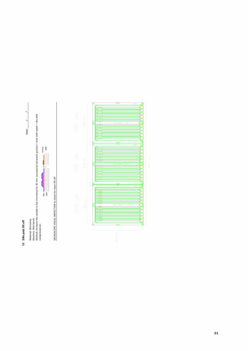
12. SiNxpa
dslift-off
Date_____/_____/______
Material:Microstrip
Machine
:Wetben
ch
Metho
d:Im
merseth
esampleinhotm
icrostrip
for4
5min.(occasio
nalultrason
icpulses)+rinsewith
water+drywith
compressedair.
MICRO
SCOPE
VISUALIN
SPEC
TIONto
che
ckfo
rclean
lift-off
91

92