Embed Size (px)
Citation preview
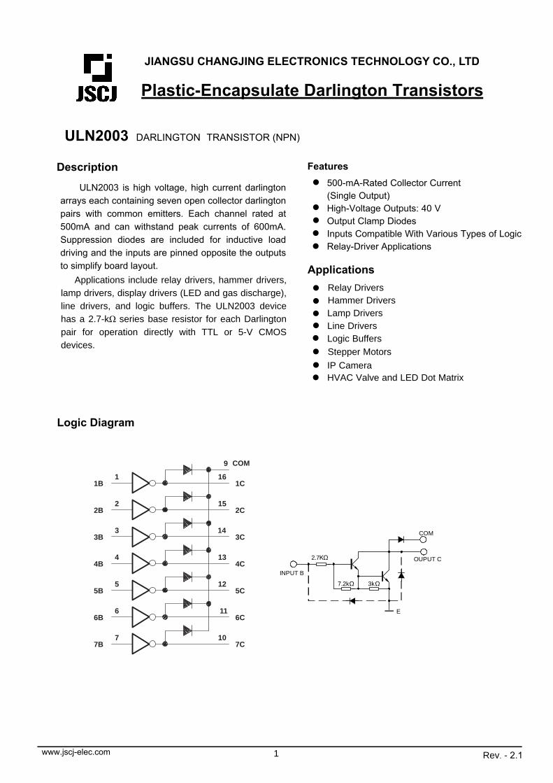
Plastic-Encapsulate Darlington Transistors
ULN2003 DARLINGTON TRANSISTOR (NPN)
Features 500-mA-Rated Collector Current
(Single Output)High-Voltage Outputs: 40 VOutput Clamp DiodesInputs Compatible With Various Types of LogicRelay-Driver Applications
Logic Diagram
ApplicationsRelay DriversHammer DriversLamp DriversLine DriversLogic BuffersStepper MotorsIP CameraHVAC Valve and LED Dot Matrix
Description ULN2003 is high voltage, high current darlington
arrays each containing seven open collector darlington pairs with common emitters. Each channel rated at 500mA and can withstand peak currents of 600mA. Suppression diodes are included for inductive load driving and the inputs are pinned opposite the outputs to simplify board layout. Applications include relay drivers, hammer drivers, lamp drivers, display drivers (LED and gas discharge), line drivers, and logic buffers. The ULN2003 device has a 2.7-kΩ series base resistor for each Darlington pair for operation directly with TTL or 5-V CMOS devices.
INPUT B
OUPUT C
COM
E
7.2k Ω 3k Ω
2.7KΩ
7C
6C
5C
4C
3C
2C
1C
COM
7
6
5
4
3
2
1
7B
6B
5B
4B
3B
2B
1B
10
11
12
13
14
15
16
9
JIANGSU CHANGJING ELECTRONICS TECHNOLOGY CO., LTD
1 Rev. - 2.1www.jscj-elec.com
11B 1C
22B 2C
33B
16
3C
44B
15
4C
55B
14
5C
66B
13
6C
77B
12
7C
8
11
GND COM
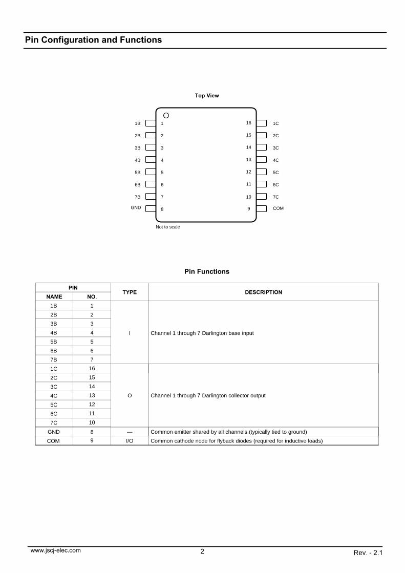
Not to scale
Top View
Pin Functions
PINTYPE DESCRIPTION
NAME NO.1B 1
I Channel 1 through 7 Darlington base input
2B 23B 34B 45B 56B 67B 7
8
1C
O Channel 1 through 7 Darlington collector output
2C3C
16
4C
15
5C
14
6C
13
7C
1211
GND9
— Common emitter shared by all channels (typically tied to ground)
COM
10
I/O Common cathode node for flyback diodes (required for inductive loads)
Pin Configuration and Functions
10
9
2www.jscj-elec.com Rev. - 2.1

PARAMETER TEST CONDITIONSULN2003
UNITMIN TYP MAX
ICEX Collector cutoff current100.0 μA
Typical Characteristics
ELECTRICAL CHARACTERISTICS (Ta=25℃ unless otherwise specified)
3www.jscj-elec.com Rev. - 2.1
ABSOLUTE MAXIMUM RATING PARAMETER SYMBOL
ULN2003UNIT
MIN TYP MAX
VO 40 V
VI
Output voltage
30 V
ICCollector current(continuous current) 500 mA
Storage Temperature Tstg -55 150 ℃
℃150TJOperating Junction Temperature
Operating Ambient Temperature TA -20 85 ℃
mA25IBBase current(continuous current)
Input voltage
VCE = 40 V, Tamb=+85℃
VCE = 40 V, Tamb=+25℃ 50.0 μA
VCES Collector-emitter saturation voltage
IC = 350 mA, IB=500uA 1.6
IC = 200 mA, IB=350uA 1.3 V
IC = 100 mA, IB=250uA 1.1
II(ON) Input current(ON) VI = 3.85 V 1.35 mA
VI(ON) Input voltage(ON)
VCE = 2.0 V, IC=200mA 2.4
VCE = 2.0 V, IC=250mA 2.7 V
VCE = 2.0 V, IC=300mA 3.0
II(OFF) Input current(OFF) VCE = 2.0 V, IC=350mA 100 μA
CI Input capacitance 30 pF
tON On delay time 50%EI to 50% EO 1.0 μs
tOFF Off delay time 50%EI to 50% EO 1.0 μs
Clamp reverse current VR = 50 V50.0
μAIR100.0
VF Clamp forward voltage IF=350mA 2.0 V
1.1
0.95
0.85
1.5
TA=+25℃
TA=+85℃
0.25
0.25
15
50
0.93
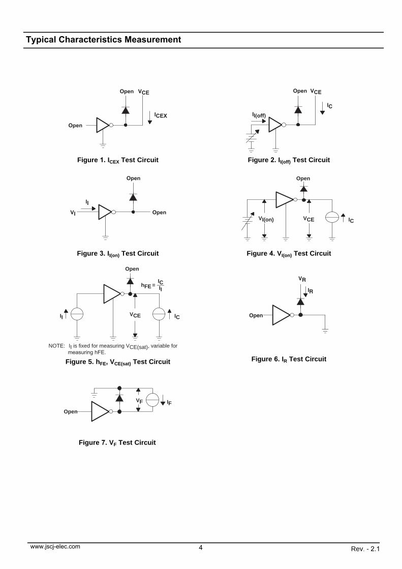
Typical Characteristics Measurement
VR
Open
IR
Open
II
OpenVI
Open VCE
IC
II(off)
Open VCE
ICEX
Open
Figure 1. ICEX Test Circuit Figure 2. II(off) Test Circuit
Figure 3. II(on) Test Circuit Figure 4. VI(on) Test Circuit
Figure 5. hFE, VCE(sat) Test Circuit Figure 6. IR Test Circuit
Figure 7. VF Test Circuit
Open
VCE ICII
hFE =ICII—
NOTE: II is fixed for measuring VCE(sat), variable for measuring hFE.
IFVF
Open
Open
VCE ICVI(on)
4www.jscj-elec.com Rev. - 2.1
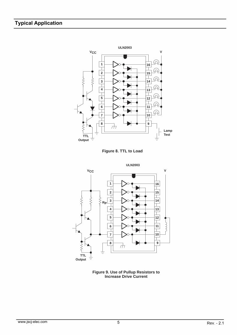
Typical Application
ULN2003
LampTestTTL
Output
VCC V
1
2
3
4
5
6
9
10
11
12
13
14
15
16
8
7
Figure 8. TTL to Load
Figure 9. Use of Pullup Resistors to Increase Drive Current
VCC V
RP
1
2
3
4
5
6
9
10
11
12
13
14
15
16
8
TTLOutput
7
ULN2003
5www.jscj-elec.com Rev. - 2.1
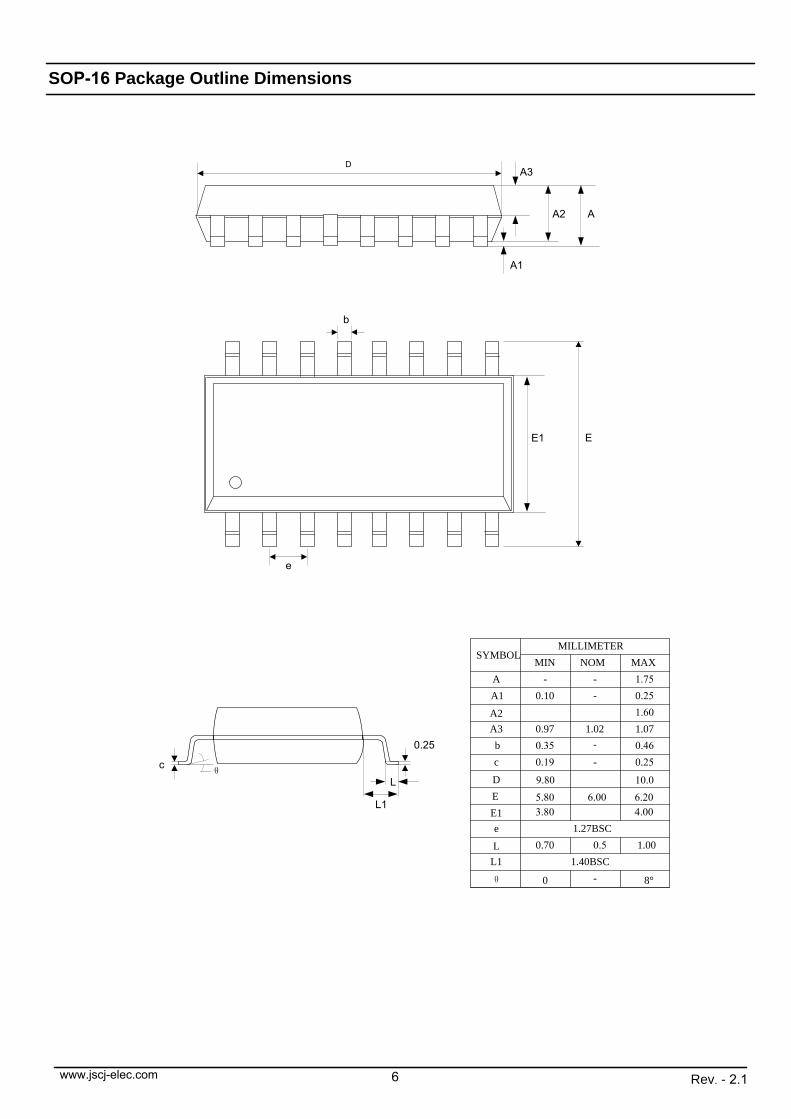
SOP-16 Package Outline Dimensions
D
e
b
AA2
A3
A1
E1 E
θL
L1
c
0.25
A
A1
A2
A3
b
c
D
E
E1
e
L
L1
θ
SYMBOLMILLIMETER
MIN MAXNOM
1.750.10 0.25
1.600.97 1.02 1.07
0.35 0.460.19 0.25
9.80 10.06.00
3.80 4.001.27BSC
0.70 1.00
1.40BSC
0 8°
-
-
-
-
-
0.5
-
5.80 6.20
6www.jscj-elec.com Rev. - 2.1
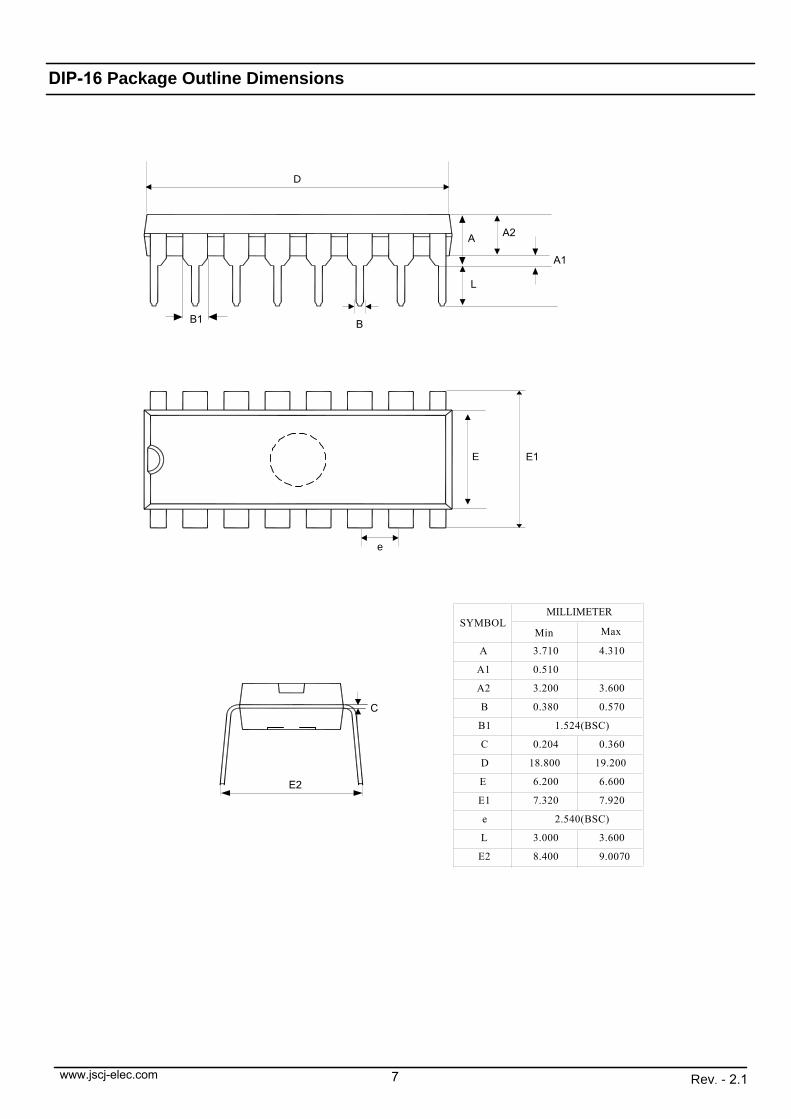
DIP-16 Package Outline Dimensions
D
e
E E1
BB1
E2
C
A A2
L
A1
Min Max
A 3.710 4.310
A1 0.510
A2 3.200 3.600
B 0.380 0.570
B1
C 0.204 0.360
D 18.800 19.200
E 6.200 6.600
E1 7.320 7.920
e
L 3.000 3.600
E2 8.400 9.0070
1.524(BSC)
2.540(BSC)
MILLIMETERSYMBOL
7www.jscj-elec.com Rev. - 2.1
Copyright © JIANGSU CHANGJING ELECTRONICS TECHNOLOGY CO., LTD.
DISCLAIMER
IMPORTANT NOTICE, PLEASE READ CAREFULLYThe information in this data sheet is intended to describe the operation and characteristics of our products. JSCJ has the right to make any modification, enhancement, improvement, correction or other changes to any content in this data sheet, including but not limited to specification parameters, circuit design and application information, without prior notice. Any person who purchases or uses JSCJ products for design shall: 1. Select products suitable for circuit application and design; 2. Design, verify and test the rationality of circuit design; 3. Procedures to ensure that the design complies with relevant laws and regulations and the requirements of such laws and regulations. JSCJ makes no warranty or representation as to the accuracy or completeness of the information contained in this data sheet and assumes no responsibility for the application or use of any of the products described in this data sheet. Without the written consent of JSCJ, this product shall not be used in occasions requiring high quality or high reliability, including but not limited to the following occasions: medical equipment, automotive electronics, military facilities and aerospace. JSCJ shall not be responsible for casualties or property losses caused by abnormal use or application of this product.
Official Website: www.jscj-elec.com