Embed Size (px)
Citation preview
POLITECNICO DI MILANO
School of Industrial Process Engineering
Master Degree in Materials Engineering and Nanotechnology
Department of Chemistry, Material and Chemical Engineering "Giulio Natta"
Self-assembled monolayer and electroless
Ni-B as alternative barrier layer and
interconnect for ULSI technology
Supervisor: Prof. Luca Magagnin
Co-Supervisor: Sr. Dr. Silvia Armini
Master Degree Thesis by:
Saracino Gianmaria
Matricola 784395
Academic Year: 2012/2013

English Abstract
iv
English Abstract
Copper represents the main option as conductive material for interconnects in the Ultra-Large
Scale Integrated (ULSI) technology since the replacement of aluminium in 1997. The introduction
was triggered by the higher conductivity and electromigration resistance offered by copper. The
necessity to avoid contact between the metal and the underlying SiO2, because of the high
interdiffusion coefficient of copper in silicon oxide, brought the semiconductor industry to
develop and place a barrier layer at the metal/dielectric interface. Common practice, today, is the
use of a double layer of Ta/TaN creating a final stack of SiO2/Ta/TaN/Cu. In the Damascene
process, a sputtering or Physical Vapour Deposition (PVD) step is employed for the deposition of
the barrier layer, and, with the same technique, also a Cu seed layer can be conformally
deposited. Such seed layer is necessary for the bottom-up filling of the vias or trenches by
electroplated copper. To keep Moore’s law verified, the future node generations will need to
continue downscaling process, together with the barrier layer stack. Due to the impossibility to
realize a conformal barrier layer of thickness below 5-6 nm, a rethinking process of the materials
and deposition techniques needs to be taken in order to win the challenge.
An “all-wet” process was developed and improved in this project as an alternative road for the
realization of a metal/barrier/dielectric stack. NiB is already known to have good barrier features
against copper diffusion, possessing good adhesion and thermal stability, together with
remarkable conductive properties. The alloy was deposited on a Si/SiO2 substrate appropriately
modified through the use of Self-Assembled Monolayers (SAMs) and catalysed by immersion in a
PdCl2 solution. The goal of this project is the evaluation of the electroless NiB thin film and line
conductivity on SAMs, on both blanket and patterned silicon, so that a good comparison with
copper and other metals may be possible.
The first part of this master thesis project is the evaluation of the SAM. Two different precursors,
(Aminoethylaminomethyl)-phenylethyltrimethoxysilane (PEDA) and (3-Trimethoxysilylpropyl)-
English Abstract
v
diethylenetriamine (DETA), both belonging to the amino-silane family, were chosen because of
their ability to create strong bonds with the SiO2 substrate and because of the presence of
negatively charged tail groups. The SAM was deposited with different techniques: on coupons
using a solvent-based solution, by vapour deposition on full wafer. Different times where used
for both depositions so that the best characteristics could be selected. Contact angle (CA) was
used as a simple technique to check the presence and quality of the organic layer, while the near-
zero thickness was measured though the use of x-ray reflectivity (XRR) and ellipsometry (EP10)
techniques. The number of top amino-groups was counted through the use of X-ray
photoelectron spectroscopy (XPS), and the same technique was employed to evaluate the
quantity of Pd uptake versus immersion time on the differently processed SAMs. A uniform
uptake of strongly bonded Pd atoms is essential to correctly catalyse the subsequent metal
deposition. Two different NiB chemistries (10% and 1% of B) were employed covering a wide
range of different deposition options (deposition time, anneal, etc.). Thin film resistivity could be
calculated through the evaluation of the thickness of the deposit, with XRR techniques, and of the
resistance, through 4-point probe measurements. Using the same technique, also the growth rate
of the film on different substrates was measured. For all the deposit adhesion, measured though
the use of a 4-point bending tool with a visual monitoring of the interface through Scanning
Electron Microscopy (SEM), proved to be strong enough to satisfy the requirements necessary for
the successive processing step of the Integrated Circuit (IC) fabrication. Chemical compositions of
the deposits were evaluated using Elastic Recoil Detection (ERD). Finally, the chemistry was
transferred to patterned coupons for the evaluation of line resistivity. Liquid SAM, with its
superior properties with respect to the vapour one, was the only deposited on the patterned
samples before the thick deposition (up to 300 nm) of NiB. The removal of excessive metal was
realized through Chemical-Mechanical Polishing (CMP), using a MECAPOL polisher. A first run
confirmed the best characteristics of DETA and NiB 1% over the other deposits. After a good
knowledge of the CMP and a good evaluation of the line filling though the use of optical
microscopy and SEM were achieved, a last run of samples was made in order to be inspected
under Transmission Electron Microscopy (TEM). Resistance of the coupons where evaluated

English Abstract
vi
though 4-point probe measurements while accurate knowledge of the section area of the line
gave the possibility to calculate resistivity. The realization of lines with resistivity below the one
of W with widths down to 14 nm was proven possible.
Italian Abstract
vii
Italian Abstract
Il rame rappresenta la principale scelta per le interconnessioni di metallo nella tecnologia ULSI dal
1997, anno in cui è subentrato all’alluminio, data la sua maggiore conducibilità rispetto a
quest’ultimo. A causa dell’alto coefficiente di diffusione del Cu all’interno del layer dielettrico di
SiO2, è stato necessario l’introduzione di uno layer intermedio che evitasse il contatto diretto tra
il metallo e il substrato. Questo ruolo è oggi svolto da un doppio strato di Ta/TaN che viene
normalmente depositato tramite PVD o sputtering, insieme ad un primo strato (seed) di rame
necessario per il successivo riempimento di vie o trincee tramite elettrodeposizione. Man mano
che le dimensioni vanno riducendosi come risultato del potenziamento e abbassamento dei costi
dei circuiti integrati, come descritto dalla legge Moore, lo strato barriera a base di tantalio, che
difficilmente riuscirà a raggiungere dimensioni inferiori ai 5 nm mantenendo accettabili
caratteristiche, dovrà essere abbandonato. Un ripensamento totale dei materiali e delle tecniche
di deposizione è quindi essenziale per permettere la creazione di barriere con caratteristiche
migliori alle tradizionali rispettando i nuovi vincoli dimensionali.
In questo progetto è stato sviluppato e migliorato un processo “all-wet” che comprende più
passaggi in soluzione per la realizzazione della struttura dielettrico/barriera/metallo. Il
conduttore è rappresentato da una lega a base di nickel-boro, “electroless” depositato su
substrato di SiO2, opportunamente funzionalizzato tramite l’uso di monostrati organici
autoassemblati (SAM). La deposizione di metallo è possibile previa catalizzazione tramite
immersione in una soluzione di PdCl2. Il NiB è noto avere buone proprietà di barriera se
accoppiato con rame: oltre a non permettere la diffusione degli atomi di silicio possiede buona
adesione sul SAM e stabilità termica. In questo progetto si tenterà di valutare le caratteristiche
del film e della linea di NiB in modo tale da avere un possibile confronto con altri metalli quali Cu
e Ni.
Italian Abstract
viii
La prima parte del progetto è centrata sulla caratterizzazione del SAM. Due differenti precursori
organici sono stati utilizzati, l’(aminoetilaminometil)-feniltrimetossisilano (PEDA) e il (3-
trimetossisililpropil)-dietilentriammina (DETA), entrambi appartenenti alla famiglia degli
ammino-silani, scelti per le loro caratteristiche di formare legami forti con il substrato e la
presenza di gruppi carichi negativamente (ammine) in coda alla molecola. Per la deposizione sono
state utilizzate una tecnica di deposizione liquida, in soluzione organica, e una vapore. Tramite la
variazione dell’angolo di contatto è stato possibile valutare l’effettiva deposizione del SAM e
quindi, tramite ellissometria (EP10) e reflettività tramite raggi x (XRR), ne è stato valutato lo
spessore. La spettroscopia fotoelettronica tramite raggi x (XPS) è stata quindi impiegata per
valutare la composizione atomica superficiale dello strato organico. Successivamente la stessa è
stata anche impiegata per stimare l’adsorbimento superficiale di palladio da parte del SAM. Nella
seconda parte del progetto ci si è concentrati più sull’ottimizzazione del processo di deposizione
electroless. Due bagni con composizioni diverse sono state utilizzate (NiB 1% e NiB 10%) e diverse
caratteristiche di deposizione (tempi di deposizione, ricottura, ecc.). La misurazione dello
spessore del film, tramite XRR, e della resistenza elettrica, attraverso misure a quattro terminali,
hanno reso possibile la misura su thin film e del tasso di crescita del film stesso. L’adesione,
misurata tramite uno strumento di piegatura su quattro punti, si è dimostrata elevata e
sufficiente, per tutti i campioni, per sostenere i successivi passaggi necessari nell’industria del
circuito integrato (IC). La composizione chimica del film di NiB al variare della profondità è stata
possibile grazie alla tecnica di analisi di richiamo elastico (ERD). La deposizione è stata quindi
trasferita sui campioni patternati dove si è cercato di isolare il caso in cui la resistività di linea
risultasse minore. La combinazione NiB 1% con DETA si è rivelata inizialmente la migliore sotto
questo punto di vista ed è quindi stata esaminata più attentamente. Una comprensione migliore
della fase di chemical mechanical polishing (CMP), tramite l’uso del polisher MECAPOL, affiancato
da immagini da microscopio ottico e da microscopio a scansione elettronica (SEM), ha portato
alla ottimizzazione del processo di creazione delle linee. A quel punto è stato possibile selezionare
i migliori campioni per essere analisi tramite microscopio a scansione a effetto tunnel (TEM). La
conoscenza esatta della sezione delle linee unita alla resistenza di queste valutata tramite

Italian Abstract
ix
misurazione a quattro terminali ha reso possibile il calcolo della resistività di siffatte linee. È stato
quindi dimostrato che è possibile depositare tramite ELD, NiB in linee con larghezze pari a 14 nm,
con resistività comparabili a tutti gli altri metalli presenti in commercio.

Table of Contents
xi
Table of Contents
CHAPTER 1: INTRODUCTION .................................................................................................. 1
1.1 NANOTECHNOLOGY ................................................................................................................ 1
1.2 COPPER INTERCONNECT TECHNOLOGY ........................................................................................ 4
1.2.1 The Damascene Process ................................................................................................ 5
1.2.2 Issues in Cu interconnections ...................................................................................... 10
1.2.3 Requirements for barrier layers .................................................................................. 11
1.3 BARRIER LAYER STATE OF ARTS ............................................................................................... 12
1.4 SELF-ASSEMBLED MONOLAYER (SAM) ..................................................................................... 14
1.4.1 SAM as advanced barrier layer in interconnect technology ....................................... 19
1.4.2 SAM deposition techniques ......................................................................................... 22
1.4.2.1 Liquid deposition ..............................................................................................................22
1.4.2.2 Vapour deposition ............................................................................................................22
1.5 ELECTROLESS DEPOSITION (ELD) ............................................................................................ 23
1.5.1 Metal Ions Source ........................................................................................................ 25
1.5.2 Reducing Agents .......................................................................................................... 25
1.5.3 Complexing Agents ...................................................................................................... 27
1.5.4 Additives ...................................................................................................................... 28
1.6 NICKEL-BORON ELECTROLESS DEPOSITION ................................................................................ 29
CHAPTER 2: AIM OF THE WORK ........................................................................................... 35
CHAPTER 3: EXPERIMENTAL TECHNIQUES ........................................................................... 38
3.1 SAMS DEPOSITION TECHNIQUE ............................................................................................... 38
3.1.1 Vapour ......................................................................................................................... 38
3.1.2 Liquid ........................................................................................................................... 40
Table of Contents
xii
3.2 CONTACT ANGLE .................................................................................................................. 40
3.3 SPECTROSCOPIC ELLIPSOMETER (EP10) ................................................................................... 42
3.1 X-RAY REFLECTIVITY (XRR) .................................................................................................... 45
3.2 X-RAY DIFFRACTIVITY (XRD) .................................................................................................. 47
3.3 TOTAL X-RAY FLUORESCENCE (TXRF) ...................................................................................... 48
3.4 FOURIER TRANSFORM INFRARED SPECTROSCOPY (FTIR) ............................................................. 49
3.5 ANAEROBIC GLOVEBOX .......................................................................................................... 51
3.6 X-RAY PHOTOELECTRON SPECTROSCOPY (XPS) ......................................................................... 52
3.7 SCANNING ELECTRON MICROSCOPE (SEM) .............................................................................. 54
3.8 TRANSMISSION ELECTRON MICROSCOPY (TEM) ........................................................................ 56
3.9 FOUR POINT PROBE .............................................................................................................. 57
3.10 CHEMICAL-MECHANICAL POLISHING ........................................................................................ 60
CHAPTER 4: SELF-ASSEMBLED MONOLAYER CHARACTERIZATION ........................................ 62
4.1 INTRODUCTION .................................................................................................................... 62
4.2 PEDA ................................................................................................................................ 64
4.2.1 Materials and Methods ............................................................................................... 64
4.2.1.1 Sample preparation ..........................................................................................................64
4.2.2 Analysis and Results .................................................................................................... 66
4.2.3 Discussion .................................................................................................................... 71
4.3 DETA ................................................................................................................................ 72
4.3.1 Materials and Methods ............................................................................................... 73
4.3.1.1 Sample preparation ..........................................................................................................73
4.3.2 Analysis and Results .................................................................................................... 73
4.3.3 Discussion .................................................................................................................... 77
4.4 OBSERVATIONS .................................................................................................................... 78
CHAPTER 5: ELECTROLESS DEPOSITION OF NIB ON SAM ...................................................... 80
5.1 INTRODUCTION .................................................................................................................... 80
Table of Contents
xiii
5.2 PALLADIUM DEPOSITION ........................................................................................................ 81
5.2.1 Materials and Methods ............................................................................................... 81
5.2.1.1 Sample preparation ..........................................................................................................81
5.2.2 Analysis and results ..................................................................................................... 82
5.2.3 Discussion .................................................................................................................... 83
5.3 ELECTROLESS DEPOSITION OF NIB ........................................................................................... 84
5.3.1 Materials and Method ................................................................................................ 84
5.3.1.1 Sample preparation ..........................................................................................................84
5.3.1.2 Analysis techniques ..........................................................................................................86
5.3.2 Thin Film Resistivity ..................................................................................................... 86
5.3.2.1 Process description ..........................................................................................................86
5.3.2.2 Results presentation ........................................................................................................88
5.3.2.3 Discussion .........................................................................................................................92
5.3.3 Growth Rate Evaluation .............................................................................................. 93
5.3.3.1 Process description ..........................................................................................................93
5.3.3.2 Results presentation ........................................................................................................93
5.3.3.3 Discussion .........................................................................................................................95
5.3.4 Adhesion Evaluation .................................................................................................... 96
5.3.5 Chemical analysis ........................................................................................................ 98
5.4 NIB IN TRENCHES ............................................................................................................... 100
5.4.1 Materials and Methods ............................................................................................. 100
5.4.2 Results Presentation and Discussion ......................................................................... 105
5.4.2.1 First run ..........................................................................................................................105
5.4.2.2 Second run......................................................................................................................106
5.4.2.3 Third run .........................................................................................................................108
5.4.3 TEM Analysis ............................................................................................................. 109
5.4.3.1 Line shape .......................................................................................................................109
5.4.3.2 Line resistivity .................................................................................................................113
CHAPTER 6: CONCLUSIONS AND FUTURE PERSPECTIVES .................................................... 118

Table of Contents
xiv
6.1 CONCLUSIONS ................................................................................................................... 118
6.2 FUTURE PERSPECTIVES ........................................................................................................ 121
REFERENCES ....................................................................................................................... 123
List of Figures
xv
List of Figures
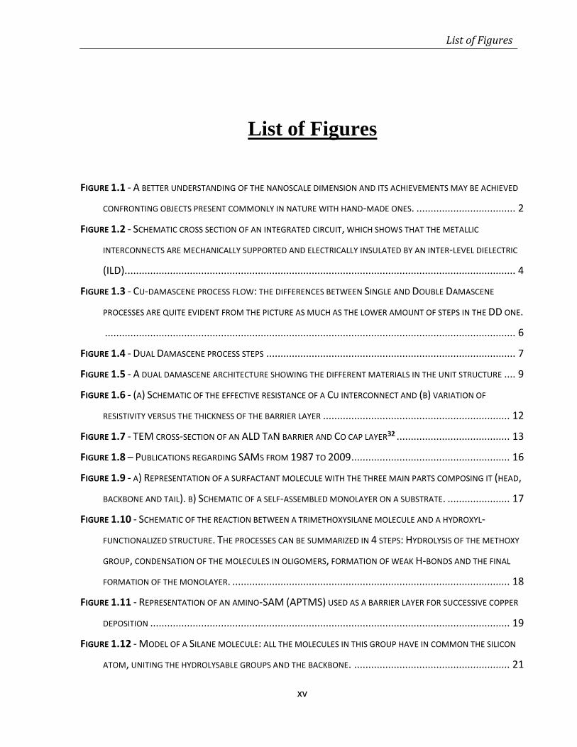
FIGURE 1.1 - A BETTER UNDERSTANDING OF THE NANOSCALE DIMENSION AND ITS ACHIEVEMENTS MAY BE ACHIEVED
CONFRONTING OBJECTS PRESENT COMMONLY IN NATURE WITH HAND-MADE ONES. ................................... 2
FIGURE 1.2 - SCHEMATIC CROSS SECTION OF AN INTEGRATED CIRCUIT, WHICH SHOWS THAT THE METALLIC
INTERCONNECTS ARE MECHANICALLY SUPPORTED AND ELECTRICALLY INSULATED BY AN INTER-LEVEL DIELECTRIC
(ILD). ......................................................................................................................................... 4
FIGURE 1.3 - CU-DAMASCENE PROCESS FLOW: THE DIFFERENCES BETWEEN SINGLE AND DOUBLE DAMASCENE
PROCESSES ARE QUITE EVIDENT FROM THE PICTURE AS MUCH AS THE LOWER AMOUNT OF STEPS IN THE DD ONE.
................................................................................................................................................. 6
FIGURE 1.4 - DUAL DAMASCENE PROCESS STEPS ........................................................................................ 7
FIGURE 1.5 - A DUAL DAMASCENE ARCHITECTURE SHOWING THE DIFFERENT MATERIALS IN THE UNIT STRUCTURE .... 9
FIGURE 1.6 - (A) SCHEMATIC OF THE EFFECTIVE RESISTANCE OF A CU INTERCONNECT AND (B) VARIATION OF
RESISTIVITY VERSUS THE THICKNESS OF THE BARRIER LAYER .................................................................. 12
FIGURE 1.7 - TEM CROSS-SECTION OF AN ALD TAN BARRIER AND CO CAP LAYER32 ........................................ 13
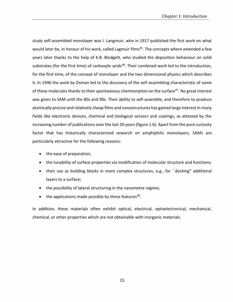
FIGURE 1.8 – PUBLICATIONS REGARDING SAMS FROM 1987 TO 2009 ........................................................ 16
FIGURE 1.9 - A) REPRESENTATION OF A SURFACTANT MOLECULE WITH THE THREE MAIN PARTS COMPOSING IT (HEAD,
BACKBONE AND TAIL). B) SCHEMATIC OF A SELF-ASSEMBLED MONOLAYER ON A SUBSTRATE. ...................... 17
FIGURE 1.10 - SCHEMATIC OF THE REACTION BETWEEN A TRIMETHOXYSILANE MOLECULE AND A HYDROXYL-
FUNCTIONALIZED STRUCTURE. THE PROCESSES CAN BE SUMMARIZED IN 4 STEPS: HYDROLYSIS OF THE METHOXY
GROUP, CONDENSATION OF THE MOLECULES IN OLIGOMERS, FORMATION OF WEAK H-BONDS AND THE FINAL
FORMATION OF THE MONOLAYER. .................................................................................................. 18
FIGURE 1.11 - REPRESENTATION OF AN AMINO-SAM (APTMS) USED AS A BARRIER LAYER FOR SUCCESSIVE COPPER
DEPOSITION ............................................................................................................................... 19
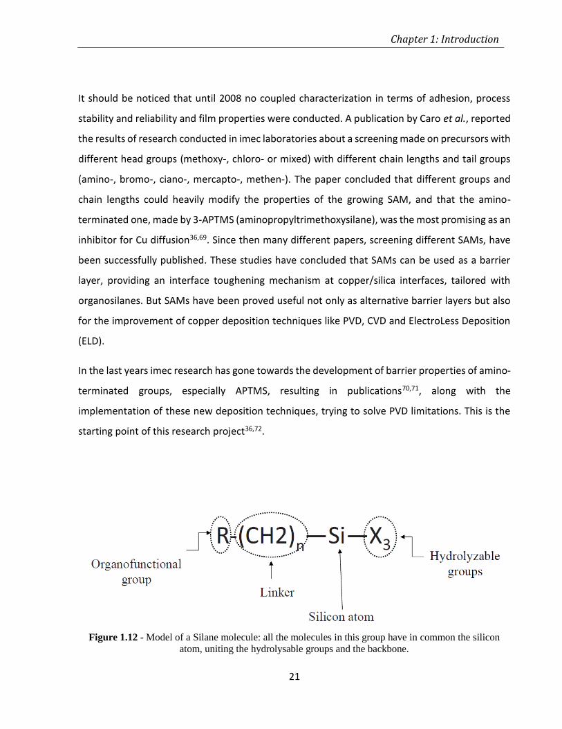
FIGURE 1.12 - MODEL OF A SILANE MOLECULE: ALL THE MOLECULES IN THIS GROUP HAVE IN COMMON THE SILICON
ATOM, UNITING THE HYDROLYSABLE GROUPS AND THE BACKBONE. ....................................................... 21
List of Figures
xvi
FIGURE 1.13 - ELECTROLESS DEPOSITION PROCESS SCHEMATIC. UP: THE REACTION IS CATALYZED BY THE SUBSTRATE.
DOWN: THE REACTION IS CATALYZED BY THE DEPOSITED METAL. ........................................................... 24
FIGURE 1.14 - NI-B PHASE DIAGRAM ..................................................................................................... 33
FIGURE 2.1 - SCHEMATIC OF THE REALIZED STACK. .................................................................................... 36
FIGURE 3.1 - THE UVO CLEANER (LEFT) AND THE SILANIZATION OVEN (RIGHT) USED DURING THE RESEARCH96. .... 39
FIGURE 3.2 - SCHEMATIC REPRESENTATION OF THE UVO CLEANING MECHANISM49 ......................................... 39
FIGURE 3.3 - A) PICTURE OF A WATER DROPLET ON A SURFACE; B) SCHEMATIC REPRESENTATION OF THE LIQUID
CONTACT ANGLE AND SURFACE TENSIONS AND ENERGIES. .................................................................... 41
FIGURE 3.4 - EFFECTS OF SIO2 SURFACE STATE ON HYDROPHILIC BEHAVIOUR. A) UVOZONE CLEANED. B) NH2-SAM
FUNCTIONALIZED......................................................................................................................... 42
FIGURE 3.5 - ELLIPSOMETER WORKING PRINCIPLE ..................................................................................... 43
FIGURE 3.6 - PICTURE OF THE ELLIPSOMETER EMPLOYED: THE LASER EMITTER, THE WAFER STAGE AND THE DETECTOR
CAN BE EASILY INDIVIDUATED. ........................................................................................................ 44
FIGURE 3.7 - DIAGRAM OF X-RAY SPECULAR REFLECTION. .......................................................................... 45
FIGURE 3.8 - XRR SPECTRUM SAMPLE: THE INFORMATION THAT CAN BE EXTRAPOLATED FROM THE PLOT ARE
DESCRIBED (INFORMATION PROVIDED BY X-RAY REFLECTIVITY)99. ......................................................... 46
FIGURE 3.9 - SCHEMATIC VIEW OF A TXRF INSTRUMENT ............................................................................ 49
FIGURE 3.10 - SCHEMATIC OF A BEAM-SPLITTER, PRESENT IN EVERY FTIR INSTRUMENT. .................................. 50
FIGURE 3.11 - SCHEMATIC OF THE TRANSFORMATION FROM AN IR SOURCE SIGNAL INCIDENT ON A
SUBSTRATE/SUBSTANCE TO INTERPRETABLE IR SPECTRA ...................................................................... 50
FIGURE 3.12 - GLOVEBOX OVERVIEW USED FOR COPPER ELD (PLAS LABS, MODEL 855-AC). ......................... 51
FIGURE 3.13 - SCHEMATIC REPRESENTATION OF AN XPS MEASUREMENT ...................................................... 53
FIGURE 3.14 - REPRESENTATION OF THE POSSIBLE PHENOMENA RELATED TO THE INTERACTION OF X-RAYS WITH A
SPECIMEN TOGETHER WITH THE INSTRUMENT USED TO COLLECT INFORMATION FROM THEM. ..................... 54
FIGURE 3.15 - SEM MICROSCOPE SCHEME .............................................................................................. 55
FIGURE 3.16 - SIMPLE SCHEMATIC OF A TRANSMISSION ELECTRON MICROSCOPE. ............................................ 56
FIGURE 3.17 - REPRESENTATION OF A FOUR-POINT PROBE USED FOR THE MEASUREMENT OF SHEET RESISTANCE. . 58
FIGURE 3.18 - CAPTION OF THE 4 NEEDLES USED TO MEASURE THE RESISTIVITY ON PATTERNED COUPONS. ........... 59
List of Figures
xvii
FIGURE 3.19 - SCHEMATIC CMP STEP. ................................................................................................... 60
FIGURE 4.1 - MOLECULAR STRUCTURE OF PEDA ...................................................................................... 64
FIGURE 4.2 - EXAMPLE OF THICKNESS DATA COLLECTED BY THE F5 TOOL. ...................................................... 69
FIGURE 4.3 - CHEMICAL STRUCTURE OF DETA ......................................................................................... 72
FIGURE 5.1 - REPRESENTATION OF THE ELD STEPS. A) DIW RINSE. B) IMMERSION IN PDCL2. C) PRE-RINSE IN DIW
& ADDITIVE M/B. D) NIB SOLUTION IMMERSION. E) POST RINSE IN DIW. ............................................ 85
FIGURE 5.2 - REPRESENTATION OF THE CRACK CREATED TO ESTIMATE THE ADHESION OF THE METAL LAYER. ......... 96
FIGURE 5.3 - ADHESION ISSUES: A LOW ADHESION MAY CAUSE THE LIFTING OF THE METAL LAYER. ...................... 97
FIGURE 5.4 - REPRESENTATION OF THE DIE: EVERY DIE IS DIVIDED IN 3 SUB DIES (A0, A1, A2). EACH COLUMN AND
ROW CONTAINS DIFFERENT FEATURES. IN THE PRESENT WORK THE 5 ΜM LONG LINE WAS MEASURED, WITH
NOMINAL DEPTH OF 60 NM. WIDTH RANGED FROM 10 NM TO 825 NM.............................................. 101
FIGURE 5.5 - PARTICULAR OF THE CMP MECAPOL TOOL. ......................................................................... 101
FIGURES 5.6 - PARTICULARS OF THE PATTERNED COUPONS AFTER CMP; THE SQUARE REPRESENT THE CONTACTS
NECESSARY FOR THE ELECTRIC MEASUREMENT OF THE RESISTANCE OF THE LINES. ................................... 103
FIGURES 5.7 – DETAILS OF THE PATTERNED SAMPLE PEDA LIQ 2H WITH NIB 10%. ...................................... 104
FIGURES 5.8 - DETAILS OF THE COUPON PEDA LIQ 5H WITH NIB 10%. ...................................................... 105
FIGURE 5.9 – TEM IMAGE OF THE SECTION OF THE PARALLEL IN THE PATTERNED COUPONS; ONLY THE MIDDLE ONE IS
ABLE TO CONDUCT, THE OTHER FOUR ARE DUMMIES. ....................................................................... 110
FIGURE 5.10 - TEM SECTION OF LINE #1. ............................................................................................. 110
FIGURE 5.11 - (LEFT) HAADF-STEM OF THE PREVIOUSLY PICTURED SECTION AND (RIGHT) DF-STEM OF IT. .... 111
FIGURE 5.12 - (FROM UPPER LEFT, CLOCKWISE) SECTION OF THE FOUR CONDUCTIVE LINES. THE EXPLOSION IN THE
SECOND LINE IS EVIDENT FROM THE IMAGE. .................................................................................... 114
List of Tables
xviii
List of Tables
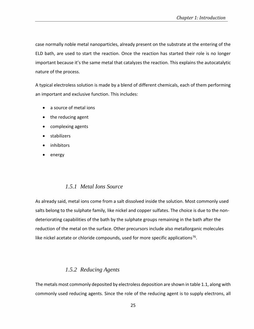
TABLE 1.1 – REDUCING AGENTS COMMONLY USED IN ELD PROCESSES. ......................................................... 26
TABLE 4.1 - SAMS PRECURSORS EMPLOYED WITH THE RESPECTIVE MOLECULAR STRUCTURE. ............................. 63
TABLE 4.2 - CA VALUES, TOGETHER WITH STANDARD DEVIATIONS, OF PEDA WET-DEPOSITED CONSIDERING
DIFFERENT DEPOSITION TIMES. ....................................................................................................... 66
TABLE 4.3 - ATOMIC CONCENTRATIONS OF THE ELEMENTS FOUND ON THE SURFACES. ...................................... 71
TABLE 4.4 - CA VALUES FOR LIQUID DEPOSITED DETA ............................................................................... 73
TABLE 4.5 - ATOMIC RELATIVE CONCENTRATIONS OF SPECIES ON THE COUPONS. ............................................. 77
TABLE 5.1 - ADHESION PROPERTIES OF NIB 10% AND 1% ON DIFFERENTLY PROCESSED BARRIER LAYERS. ............ 98
TABLE 5.2 - ATOMIC SPECIES PRESENT IN THE COUPONS. ............................................................................ 99
TABLE 5.3 - LINE DIMENSION AND RESISTIVITY AS EVALUATED FROM TEM. ................................................. 116
List of Plots
xix
List of Plots
PLOT 4.1 - CONTACT ANGLE VALUES OF VAPOUR DEPOSITED PEDA, FOR 1H AND 30' DEPOSITION. .................... 67
PLOT 4.2 - XRR PLOTS OF PEDA SAM FOR DIFFERENT DEPOSITION TIMES. THE PLOT IS PRESENTED IN TERMS OF
REFLECTIVITY VALUE OF THE X-RAY VS THE ANGLE (2Θ) OF REFLECTION. .................................................. 68
PLOT 4.3 - THICKNESSES VALUES OF PEDA VS TIME. TWO DIFFERENT MEASURES, MADE WITH TWO DIFFERENT
MEASURING SYSTEMS ARE PRESENTED: ONE THROUGH XRR, ONE EMPLOYING ELLIPSOMETRY. .................... 68
PLOT 4.4 - THICKNESS VALUE, MEASURED THROUGH F5 INSTRUMENT FOR DEPOSITION TIMES OF 30' AND 1H. ..... 69
PLOT 4.5 - ATOM COUNT VERSUS THE BONDS BINDING ENERGY: FROM THESE PLOTS IT IS POSSIBLE TO HAVE AN
ESTIMATION OF THE ATOMIC PERCENTAGES IN THE SURFACE. ............................................................... 70
PLOT 4.6 - CONTACT ANGLE VALUES OF VAPOUR DEPOSITED PEDA, FOR 1H AND 30' DEPOSITION. .................... 74
PLOT 4.7 - XRR PLOTS OF DETA SAM FOR DIFFERENT DEPOSITION TIMES. LIKE PLOT 4.1 EVERY CURVE REPRESENT,
FOR EVERY A DIFFERENT DEPOSITION TIME, THE REFLECTIVITY VS THE ANGLE (2Θ) OF REFLECTION. ............... 75
PLOT 4.8 - THICKNESSES VALUES OF DETA VS TIME. THE TWO DIFFERENT MEASURES, MADE THROUGH THE USE OF
THE XRR METHOD AN ELLIPSOMETRY PRESENTED: ONE THROUGH XRR, ONE EMPLOYING ELLIPSOMETRY. .... 75
PLOT 4.9 - THICKNESS VALUE, MEASURED THROUGH F5 INSTRUMENT FOR DEPOSITION TIMES OF DETA OF 30' AND
1H. .......................................................................................................................................... 76
PLOT 5.1 - ATOMIC COUNT OF PD AND CL ATOMS AFTER PALLADIUM DEPOSITION ON LIQUID SAM. ................... 82
PLOT 5.2 - ATOMIC COUNT OF PD AND CL ATOMS AFTER PALLADIUM DEPOSITION ON VAPOUR PROCESSED SAM. . 83
PLOT 5.3 - RESISTIVITY DATA OF NIB10% PROCESSED ON PEDA LIQ 2H AND 5H. ........................................... 89
PLOT 5.4 - RESISTIVITY DATA OF NIB10% PROCESSED ON DETA LIQ 2H AND 5H. ........................................... 89
PLOT 5.5 - RESISTIVITY DATA OF NIB1% PROCESSED ON PEDA LIQ 2H AND 5H .............................................. 90
PLOT 5.6 - RESISTIVITY DATA OF NIB1% PROCESSED ON DETA LIQ 2H AND 5H. ............................................. 90
PLOT 5.7 - RESISTIVITY DATA OF NIB10% ON VAPOUR DEPOSITED (1H AND 30') PEDA AND 30' DETA ............ 91
PLOT 5.8 - RESISTIVITY DATA OF NIB1% ON VAPOUR DEPOSITED (1H AND 30') PEDA AND 30' DETA. ............. 92
PLOT 5.9 - GROWTH RATE STUDY OF THE NIB 1% CHEMISTRY. .................................................................... 94
List of Plots
xx
PLOT 5.10 - GROWTH RATE STUDY OF THE NIB 10%. THE BLACK LINES REPRESENT THE THREE LINEAR TREND LINES.
............................................................................................................................................... 94
PLOT 5.11 - TWO EXAMPLES OF CHEMICAL TEST MADE ON THE SURFACES OF THE TWO FRACTURE PLANES. .......... 97
PLOT 5.12 – (LEFT) SPECTRUM OBTAINED FROM THE ERD MEASUREMENT; THE GRAPH IS PRESENTED IN TERMS OF
THE TIME OF FLIGHT OF THE DETACHED ATOMS FROM THE SURFACE VERSUS THE ENERGY POSSESSED. A DEPTH
GRAPH (RIGHT) CAN BE THEN OBTAINED. ......................................................................................... 99
PLOT 5.13 - RESITIVITY DATA OF THE FIRST RUN ON PATTERNED COUPONS. .................................................. 106
PLOT 5.14 - RESISTIVITY DATA OF THE SECOND RUN OF PATTERNED COUPONS (THE FIRST ONE HAS BEEN KEPT TO
PERMIT A GOOD CONFRONT). ...................................................................................................... 107
PLOT 5.15 - RUN 3 OF PATTERNED COUPONS. ....................................................................................... 108
PLOT 5.16 - ELEMENT COUNT MADE BY HAADF-STEM ......................................................................... 112
PLOT 5.17 - RESISTIVITY DATA, TOGETHER WITH THE SAMPLES STEM PROCESSED. ....................................... 115

xxi
Chapter 1: Introduction
1
Chapter 1: Introduction
This brief introductory chapter is presented to the reader in order to allow him to familiarize with
the subjects covered in this master thesis project. Three main topics will be of particular interest,
which will be covered in this chapter. The first one will focus on the research field in which this
work was developed: that is the integrated circuit (IC) technology; the second, on the
revolutionary characteristics and properties of Self-Assembled Monolayers (SAM) and the final
part of the chapter will be dedicated to an analysis of the electroless deposition of metals, in
particular nickel, exposing advantages and issues of this technique.
1.1 Nanotechnology
When talking about Nanotechnology, the famous speech “There is plenty of space at the bottom”,
made by Richard P. Feynman in 1959 cannot go uncited. The lecturer, during his talk at Caltech
University, envisaged the possibility to create smaller and smaller machines, enabling us to
manipulate the single atoms and molecules1. The speech is often held as an inspiration for the
research at lower scales, i.e. for the field of research that would later be called nanotechnology.
But this word was actually introduced for the first time only in 1983 by Japanese scientist Norio
Taniguchi . who gave the following definition “’Nano-technology' mainly consists of the
processing of, separation, consolidation, and deformation of materials by one atom or one
molecule”2.
In the last years many definitions of nanotechnology have been proposed, mainly focusing on the
possibility to nano-manipulate objects. The emphasis on this aspect is not causal: it is this that
distinguishes nanotechnology from chemistry, with which is often compared. While in the latter
Chapter 1: Introduction
2
the motion of objects like molecules and atom is random and uncontrolled (in the limits defined
by the free energy possessed by these elements) in the former a non-random eutactic
environment needs to be available to achieve the desired control3. In this sense the US Foresight
Institute gave a rather appreciated definition. According to, it nanotechnology is a group of
emerging technologies in which the structure of matter is controlled up to the nanometre scale
to produce novel materials and devices that have useful and unique properties4.
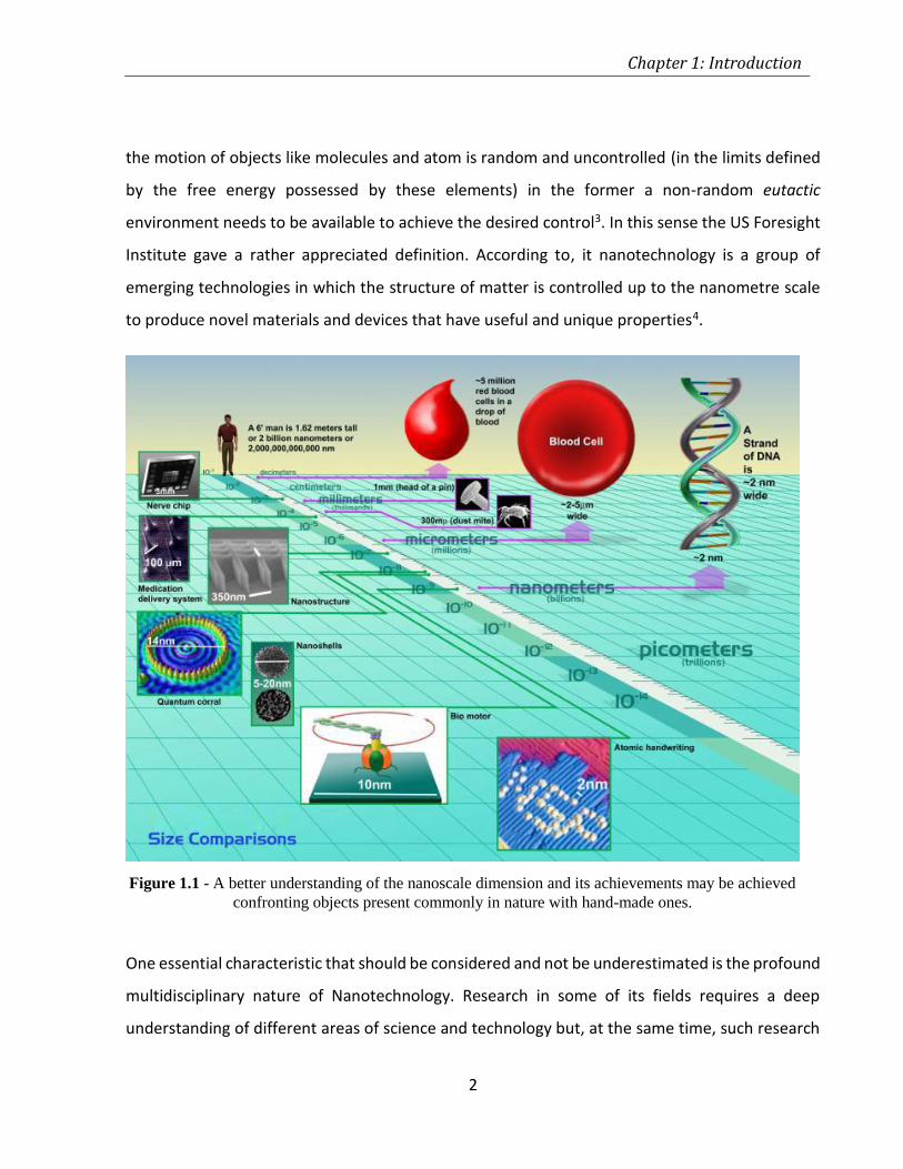
One essential characteristic that should be considered and not be underestimated is the profound
multidisciplinary nature of Nanotechnology. Research in some of its fields requires a deep
understanding of different areas of science and technology but, at the same time, such research
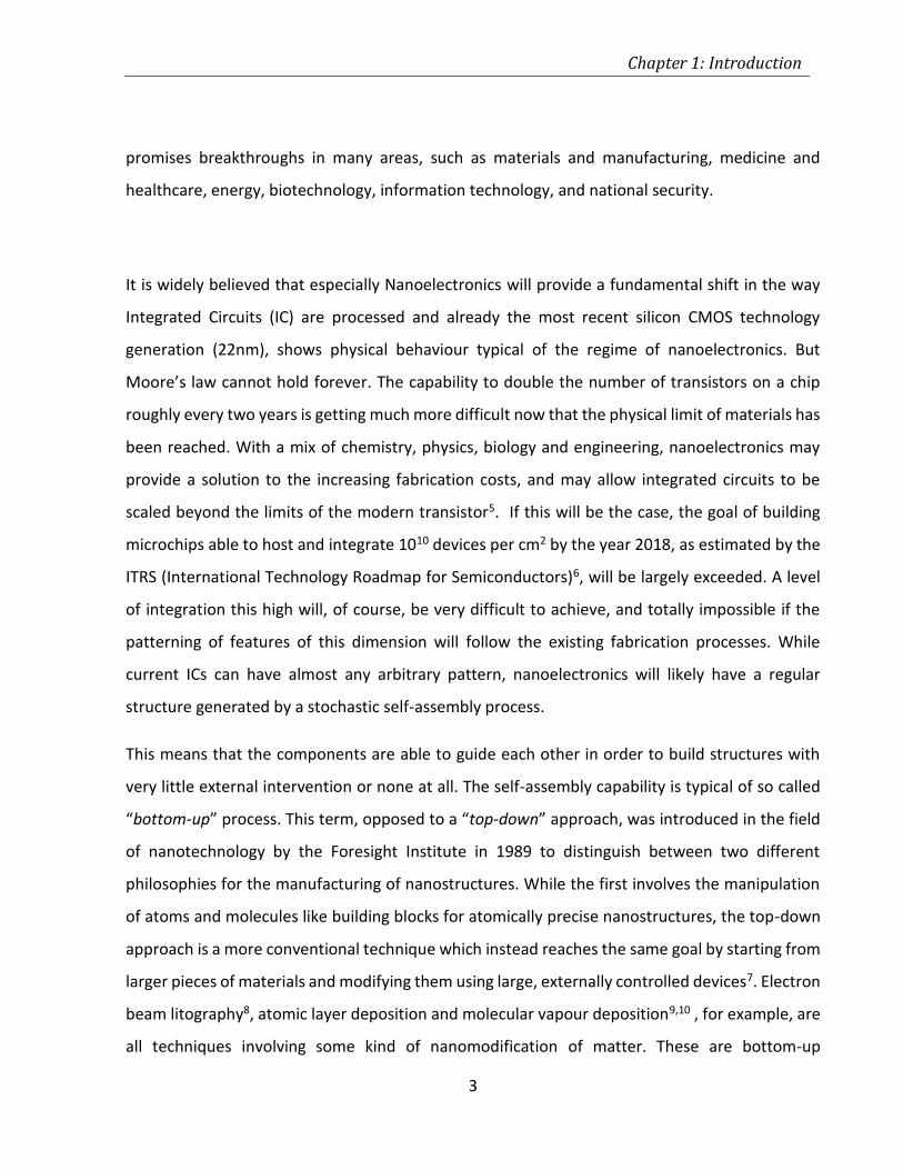
Figure 1.1 - A better understanding of the nanoscale dimension and its achievements may be achieved
confronting objects present commonly in nature with hand-made ones.
Chapter 1: Introduction
3
promises breakthroughs in many areas, such as materials and manufacturing, medicine and
healthcare, energy, biotechnology, information technology, and national security.
It is widely believed that especially Nanoelectronics will provide a fundamental shift in the way
Integrated Circuits (IC) are processed and already the most recent silicon CMOS technology
generation (22nm), shows physical behaviour typical of the regime of nanoelectronics. But
Moore’s law cannot hold forever. The capability to double the number of transistors on a chip
roughly every two years is getting much more difficult now that the physical limit of materials has
been reached. With a mix of chemistry, physics, biology and engineering, nanoelectronics may
provide a solution to the increasing fabrication costs, and may allow integrated circuits to be
scaled beyond the limits of the modern transistor5. If this will be the case, the goal of building
microchips able to host and integrate 1010 devices per cm2 by the year 2018, as estimated by the
ITRS (International Technology Roadmap for Semiconductors)6, will be largely exceeded. A level
of integration this high will, of course, be very difficult to achieve, and totally impossible if the
patterning of features of this dimension will follow the existing fabrication processes. While
current ICs can have almost any arbitrary pattern, nanoelectronics will likely have a regular
structure generated by a stochastic self-assembly process.
This means that the components are able to guide each other in order to build structures with
very little external intervention or none at all. The self-assembly capability is typical of so called
“bottom-up” process. This term, opposed to a “top-down” approach, was introduced in the field
of nanotechnology by the Foresight Institute in 1989 to distinguish between two different
philosophies for the manufacturing of nanostructures. While the first involves the manipulation
of atoms and molecules like building blocks for atomically precise nanostructures, the top-down
approach is a more conventional technique which instead reaches the same goal by starting from
larger pieces of materials and modifying them using large, externally controlled devices7. Electron
beam litography8, atomic layer deposition and molecular vapour deposition9,10 , for example, are
all techniques involving some kind of nanomodification of matter. These are bottom-up
Chapter 1: Introduction
4
techniques largely used today in many engineering fields. Self-Assembly Monolayers (SAM) also
have shown promising properties with their tuneable properties. Instead a commonly used top-
down technique is dry etching of bulk materials, useful in the creation of circuits on the top
surface of silicon microchips11.
Nanoelectronics and, more widely, Nanotechnology have the potential to deeply change
everyday life in ways that today cannot be predicted, while the numbers of fields where
nanotechnology will be employed will largely increase along with the decreasing of technology
prices.
1.2 Copper interconnect technology
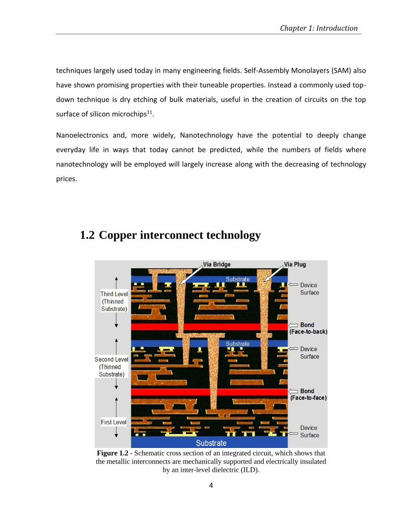
Figure 1.2 - Schematic cross section of an integrated circuit, which shows that
the metallic interconnects are mechanically supported and electrically insulated
by an inter-level dielectric (ILD).
Chapter 1: Introduction
5
Interconnect technology represents an area of electrical engineering regarding the metallization
process necessary to produce electrical conductive lines for the interconnection of the individual
semiconductor devices as shown in Fig. 1.2.
An overview of how interconnections are produced, which materials are employed and how these
have been developed, will be given in the following paragraphs.
1.2.1 The Damascene Process
Copper has represented the fundamental material for the realization of interconnections in
semiconductor integrated circuits since 199712. Previously, the lack of volatile Cu compounds
made patterning procedures practically impossible, consequently making aluminium the best
choice from the start of the IC industry. The destiny of aluminium was anyway already
foreseeable: copper wires conduct electricity with about 40 percent less resistance than
aluminium wires, which results in a 15 percent burst in microprocessor speed due to the decrease
of RC delay, which, in turn, increases the IC speed. Copper wires are also significantly more
durable and 100 times more reliable over time, and can be shrunk to smaller sizes than
aluminium. Also copper gives the possibility to add more layers of interconnections by introducing
new manufacturing technologies.
Replacement of aluminium with copper represented a big challenge for semiconductor engineers.
Aluminium can be deposited over the entire wafer surface and then patterned by reactive ion
etching (RIE), while all efforts to apply the same process on copper failed. Since copper cannot be
patterned, a new approach had to be developed in order to have a good filling of the patterned
dielectric layers.
Chapter 1: Introduction
6
Various forms of PVD (sputtering, deposition etch, electron cyclotron resonance) as well as CVDs
were examined initially13. A sub-conformal deposition of the metal in the trenches or vias,
responsible for the formation of voids and seams, was the main reason the processes were
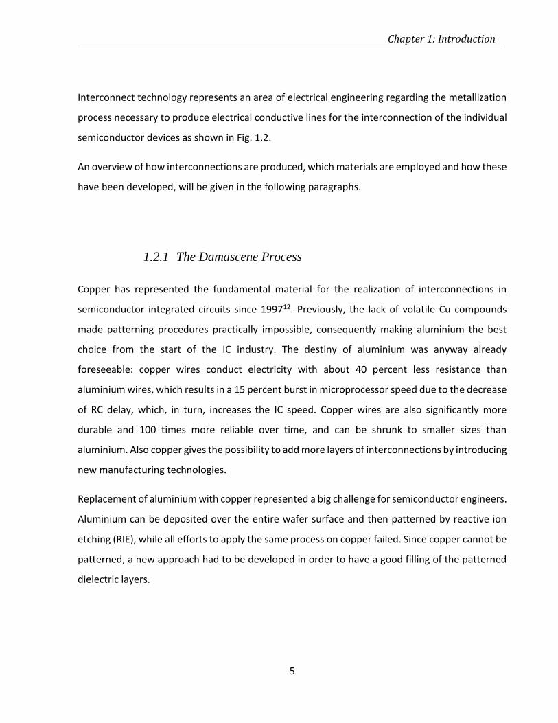
abandoned 14. At the end of the century, copper Damascene processes were introduced and the
Figure 1.3 - Cu-damascene process flow: the differences between Single and
Double Damascene processes are quite evident from the picture as much as
the lower amount of steps in the DD one.
Chapter 1: Introduction
7
century-old chemical mechanical polishing (CMP) procedure was renewed to integrate copper in
deep sub-micron level circuitry. Superfilling, which refers to a filling process where a higher
deposition rate is achieved at the bottom of the trench or via, with respect to the sides, resulting
in a void-free filling, played a pivotal role in the success of this technology15. The damascene
process can be either a single Damascene (SD) or a dual Damascene (DD), as can be seen in figure
1.2. The difference between the simple SD process and the DD process is that in the DD process
one metal deposition step and one CMP step are eliminated (as well as the dielectric deposition
step). The reduction in the number of processing steps made DD more attractive than its twin
single Damascene process.
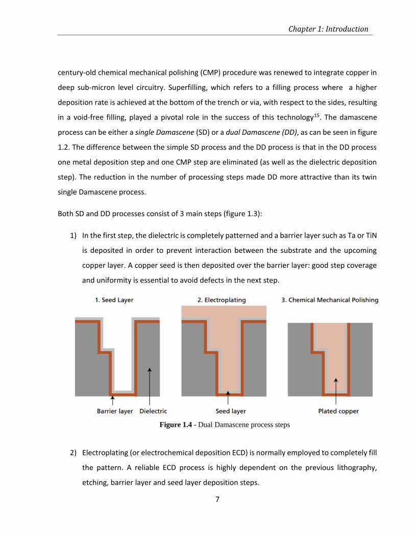
Both SD and DD processes consist of 3 main steps (figure 1.3):
1) In the first step, the dielectric is completely patterned and a barrier layer such as Ta or TiN
is deposited in order to prevent interaction between the substrate and the upcoming
copper layer. A copper seed is then deposited over the barrier layer: good step coverage
and uniformity is essential to avoid defects in the next step.
2) Electroplating (or electrochemical deposition ECD) is normally employed to completely fill
the pattern. A reliable ECD process is highly dependent on the previous lithography,
etching, barrier layer and seed layer deposition steps.
Figure 1.4 - Dual Damascene process steps
Chapter 1: Introduction
8
3) The chemical mechanical polishing (CMP) step is essential to remove excessive copper,
due to the impossibility for it to be etched away. CMP is able to provide globally planar
surface but only if the original topography is amenable to global planarity. It consists of a
synergistic process that removes material through a mechanical action of a solution
(slurry) containing abrasive particles like silica and alumina, while a chemical attack is
carried out by the hydrogen peroxide contained in the slurry that manages to oxidize the
metal layer16,17.
The patterning of the dielectric is normally made through the formation of a cap layer (constituted
of silicon compound, SixNy normally) which is, in turn, coated with a photoresist material and
patterned through the lithographic step. Anisotropic etching is then able to cut through the
surface hard mask (plasma SixNy is often employed) without attacking the underlying substrate
thanks to an embedded etch-stop layer.
The ability of the CMP to stop the planarization once the dielectric layer has been exposed, with
the possibility to remove the copper in a planar fashion, leads to the realization of successive
layers of insulator and copper, creating a multilayer (more than 10) interconnection structure.
Five different DD processes were studied over the last few years. Nowadays only two are currently
in mainstream production: embedded-via first and embedded-trench first. The difference
between them is the way the etching step is carried out. In the first case the etching attacks both
layers on which the DD process is done. A second etching is made on the top layer that has been
previously coated with photoresist. In the embedded-trench first approach the etching phase
attacks one layer at a time. The major drawback in this case is that, after the trench is etched, the
photoresist that is applied for the via-step will completely fill the feature. As a result, the PR can
be said to be pooled in the trench, leaving an extra thick resist layer right in the area where via
holes are to be patterned. This creates a difficult situation to fabricate fine structures for via holes.
For smaller trenches the embedded-via first approach has been widely accepted in industry18.
Chapter 1: Introduction
9
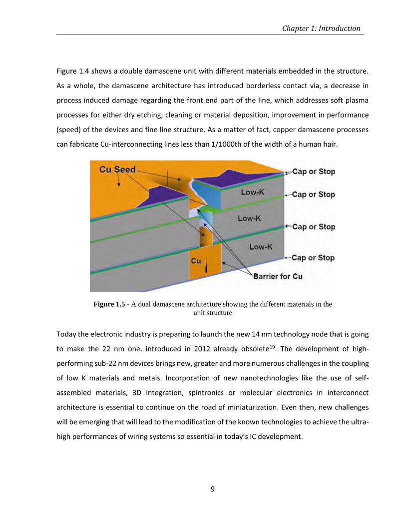
Figure 1.4 shows a double damascene unit with different materials embedded in the structure.
As a whole, the damascene architecture has introduced borderless contact via, a decrease in
process induced damage regarding the front end part of the line, which addresses soft plasma
processes for either dry etching, cleaning or material deposition, improvement in performance
(speed) of the devices and fine line structure. As a matter of fact, copper damascene processes
can fabricate Cu-interconnecting lines less than 1/1000th of the width of a human hair.
Today the electronic industry is preparing to launch the new 14 nm technology node that is going
to make the 22 nm one, introduced in 2012 already obsolete19. The development of high-
performing sub-22 nm devices brings new, greater and more numerous challenges in the coupling
of low K materials and metals. Incorporation of new nanotechnologies like the use of self-
assembled materials, 3D integration, spintronics or molecular electronics in interconnect
architecture is essential to continue on the road of miniaturization. Even then, new challenges
will be emerging that will lead to the modification of the known technologies to achieve the ultra-
high performances of wiring systems so essential in today’s IC development.
Figure 1.5 - A dual damascene architecture showing the different materials in the
unit structure
Chapter 1: Introduction
10
1.2.2 Issues in Cu interconnections
In the previous chapter we described how the deposition process had to be rethought after the
revolution from an aluminium based industry to a copper based one. Apart from the absence of
volatile compounds, formerly mentioned, there are several other difficulties encountered in the
use of Cu interconnect. The issues are mainly caused by some peculiar chemical and mechanical
properties of copper. It is worth mentioning, for example, that copper does not form a stable
oxide, as instead aluminium does. Also, in contrast to other three-dimensional (3D) transition
metals, Cu has a very high diffusivity in silicon (diffusion coefficient D = 3 × 10⁻⁴ cm2/s)20, due to
its small atomic radius and weak interaction with the silicon lattice. Furthermore copper interacts
strongly with silicon, forming silicides (Cu3Si) starting from 200 °C, modifying its atomic
structure21.
Copper diffusion normally happens through the migration of its ions Cu+/++, which is enhanced by
the presence of applied currents22. Instead the formation of copper ions is enhanced by a series
of factors like high humidity, presence of impurities on the top surfaces and/or in the bulk of the
dielectric material23. The presence of copper in silicon oxide impacts the function of the active
elements by creating short trap state or causing shortcuts in case of agglomeration24. Moreover
copper shows low adhesion on underlying silicon oxide layers due to the difference in the free
energy of formation of copper oxide against that of silicon oxide. The oxide is normally formed by
a combination of CuO and Cu2O and, as already mentioned, these oxides present very different
properties with respect to alumina, Al2O3. While alumina provides very good protective properties
for aluminium technology processes, copper oxides show completely opposite properties.
A cap layer has been used, since the birth of copper interconnect technology, to avoid oxidation,
corrosion, interface diffusion and other issues in copper. A barrier layer, sandwiched between
copper interconnections and the dielectric layer, was instead introduced to prevent chemical
contact between the dielectric materials and copper.
Chapter 1: Introduction
11
1.2.3 Requirements for barrier layers
An ideal barrier layer should provide an insurmountable boundary between copper and the
dielectric layer. This implies that crystalline materials should be avoided, due to the presence of
faster diffusion paths like grain boundaries. As a general rule, the higher the crystallization
temperature the higher the diffusion-blocking of the material25 will be. Crystalline materials may
be employed if grain boundaries are avoided (impurity atoms like O, N, C, Zr are useful in this
sense) or if they are present but their directionality is perpendicular to the film surface. A basic
requirement for barrier/interconnects stack is to show a resistivity as low as possible: the
presence of the barrier layer will surely cause a decrease in the net cross-section occupied by
copper, resulting in a higher resistivity of the line or via. It is important then to scale down the
barrier films, even more so, since the copper lines are undergoing a shrinking process.
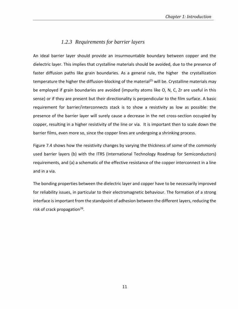
Figure 7.4 shows how the resistivity changes by varying the thickness of some of the commonly
used barrier layers (b) with the ITRS (International Technology Roadmap for Semiconductors)
requirements, and (a) a schematic of the effective resistance of the copper interconnect in a line
and in a via.
The bonding properties between the dielectric layer and copper have to be necessarily improved
for reliability issues, in particular to their electromagnetic behaviour. The formation of a strong
interface is important from the standpoint of adhesion between the different layers, reducing the
risk of crack propagation26.
Chapter 1: Introduction
12
Also the wetting capability of the barrier film with respect to the liquid metal should be
considered. A good wetting will provide low roughness and will affect the crystallographic
orientation of the growing layer. Last, but not least, thermodynamics and kinetics have always to
be taken into account to foresee possible undesired reactions between different layers18.
1.3 Barrier Layer State of Arts
A conventional barrier layer in advanced ULCI metallization is normally composed of a bilayer of
tantalum (Ta) and tantalum nitride (TaN). The implementation of a double Ta/TaNx was first
introduced in reference 27. Such structure is able to adhere very well to the substrate through the
strong TaNx/SiO2 interface, whereas the Ta has a high adherence towards the metal layer. The
bilayer is also characterized by a thermal stability that is at least as high as the most stable single
layer24. With a density of 16.3 and c/a 6.5 g/cm3, the double film can reach values of copper
diffusion coefficient higher than 2∙10-14 cm2/s and avoids the formation of copper silicides up to
700 °C. The deposition was carried out through a double process: PVD for the Ta layer and ALD
for TaNx. At the present day a PVD process is successfully employed for both films.
Figure 1.6 - (a) Schematic of the effective resistance of a Cu interconnect and (b) variation of
resistivity versus the thickness of the barrier layer
Chapter 1: Introduction
13
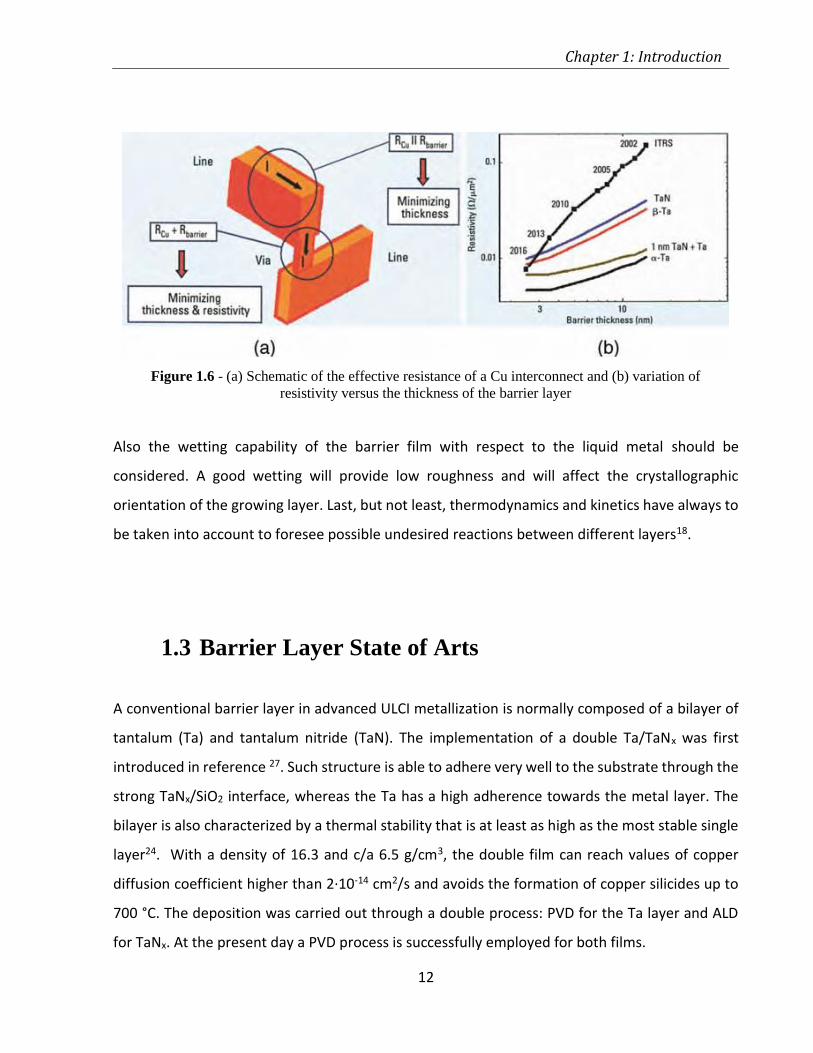
The described structure and processing is
not free of issues. It is expected that these
barriers, together with the PVD copper
seed layer, will not be able to meet the
future technology requirements. A thinner
and continuous copper barrier/seed with
good step coverage and no overhang for
excellent copper gap fills is necessary as the
dimensions of the trench or via hole shrinks
and the aspect ratio increases28. The PVD
process does not maintain these
requirements for barrier layers thinner
than 5-6 nm and furthermore it shows an
excessive resistivity compared to that of copper (ρTaN=350μΩ∙cm29).
Therefore a radical improvement of the PVD Ta/TaNx process or a change in the used materials
or deposition modes is expected in order to meet the new interconnect size as well as good
barrier layer characteristics.
Techniques like advanced PVD (ENhanced COverage Resputtering), CVD and ALCVD (Atomic Layer
Chemical Vapour Deposition) have demonstrated better conformality characteristics than
traditional PVD30,31. A lot of effort has been made in recent years to implement Atomic Layer
Deposition (ALD) in order to overcome the deposition issues of PVD, especially conformality and
thickness32. ALD presents many similarities to PVD, like the use of gas precursors, but shows
interesting differences. In particular the self-limiting character of the process can be exploited to
achieve high uniformity deposits also in narrow trenches, holes and vias. Different compounds
can be deposited with this technique, especially transitional metals and their nitrides (Ta, Ti, W)33.
Pressure is today being put on new ultra-low-k materials to reduce the RC delay, in order to
achieve high speeds in nanoscale circuits34, for future scaled down interconnect technologies.
Figure 1.7 - TEM cross-section of an ALD TaN
barrier and Co cap layer32
Chapter 1: Introduction
14
Porous low-k materials have been under study in recent years as a new class of materials able to
meet tighter requirements. These materials present new issues that have to be compensated by
the barrier layer30,35. Low mechanical strength, porous sidewalls of vias and trenches will be
present if conventional PVD is used.
As we will see in the next paragraphs, Self-Assembled Monolayers (SAM) alternative barriers,
even if presenting similar principles to ALD precursors, offer interesting advantages. No strict
need of vacuum, single cycle deposition for the achievement of conformal, near-zero thickness
layers, even at room temperature and pore sealing characteristics can be achieved by tuning the
SAM precursor structure36.
1.4 Self-assembled monolayer (SAM)
The term Self-Assembly Monolayer (SAM) has been cited earlier in this work without providing a
good explanation of its meaning. This paragraph will provide the reader with a good insight in the
SAMs original and novel properties.
A self-assembled monolayer is an ordered thin layer, formed by organic molecules able to auto-
arrange spontaneously in an ordinate manner on top of appropriate substrates with which it
normally has a strong interaction37. Complex hierarchical structures can be formed from small
building-block, involving multiple energy scales and degrees of freedom38. As already said in
paragraph 1.1, the self-assembling ability of SAMs allows them to be considered a typical
“bottom-up” approach.
Organic films have always captured the attention of many scientists for centuries due to their
particular behaviour. Already Benjamin Franklin more than 200 years ago studied the calming
influence of oil on water waves39. In the 19th century, Pockels prepared monolayers at the air-
water interface40–42, followed by the works of Rayleigh43, Hardy44 and others. The first to actually
Chapter 1: Introduction
15
study self-assembled monolayer was I. Langmuir, who in 1917 published the first work on what
would later be, in honour of his work, called Lagmuir films45. The concepts where extended a few
years later thanks to the help of K.B. Blodgett, who studied the deposition behaviour on solid
substrates (for the first time) of carboxylic acids46. Their combined work led to the introduction,
for the first time, of the concept of monolayer and the two dimensional physics which describes
it. In 1946 the work by Zisman led to the discovery of the self-assembling characteristic of some
of these molecules thanks to their spontaneous chemisorption on the surface47. No great interest
was given to SAM until the 80s and 90s. Their ability to self-assemble, and therefore to produce
atomically precise and relatively cheap films and nanostructures has gained large interest in many
fields like electronic devices, chemical and biological sensors and coatings, as attested by the
increasing number of publications over the last 20 years (figure 1.6). Apart from the pure curiosity
factor that has historically characterized research on amphiphilic monolayers, SAMs are
particularly attractive for the following reasons:
the ease of preparation;
the tunability of surface properties via modification of molecular structure and functions;
their use as building blocks in more complex structures, e.g., for ``docking'' additional
layers to a surface;
the possibility of lateral structuring in the nanometre regime;
the applications made possible by these features38.
In addition, these materials often exhibit optical, electrical, optoelectronical, mechanical,
chemical, or other properties which are not obtainable with inorganic materials.
Chapter 1: Introduction
16
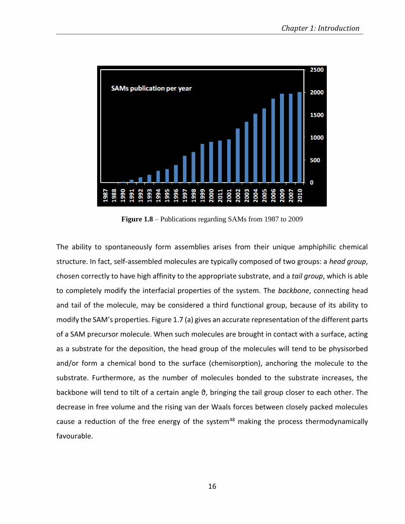
The ability to spontaneously form assemblies arises from their unique amphiphilic chemical
structure. In fact, self-assembled molecules are typically composed of two groups: a head group,
chosen correctly to have high affinity to the appropriate substrate, and a tail group, which is able
to completely modify the interfacial properties of the system. The backbone, connecting head
and tail of the molecule, may be considered a third functional group, because of its ability to
modify the SAM’s properties. Figure 1.7 (a) gives an accurate representation of the different parts
of a SAM precursor molecule. When such molecules are brought in contact with a surface, acting
as a substrate for the deposition, the head group of the molecules will tend to be physisorbed
and/or form a chemical bond to the surface (chemisorption), anchoring the molecule to the
substrate. Furthermore, as the number of molecules bonded to the substrate increases, the
backbone will tend to tilt of a certain angle ϑ, bringing the tail group closer to each other. The
decrease in free volume and the rising van der Waals forces between closely packed molecules
cause a reduction of the free energy of the system48 making the process thermodynamically
favourable.
Figure 1.8 – Publications regarding SAMs from 1987 to 2009
Chapter 1: Introduction
17
The possibility to tailor head and tail groups of the constituent as needed enables an accurate
design of the surfaces and interfaces and the selective deposit of SAMs on a specific substrate.
End groups can be chosen to allow for further physical or chemical functionalization essential for
the employment of SAMs as intermediate layers for successive depositions49. We can add
hydrophilic end groups (i.e. –OH, -NH2, -COOH) or hydrophobic ones (-CH3) to vary the wetting of
a substrate and the interfacial properties of it. On the other hand an appropriate head group can
be selected in order to react with the substrate. Since the head group has to be selected wisely
considering the chemical functional group defining the substrate (while the rest of the molecules
can be almost freely chosen), this “chemisorption pair” is used to classify the specific system in
the following38. One of the most popular is probably the group of thiols (-SH): they have high
affinity with metal substrates like Au50 (111). Alkoxy (-Si(OCH3)3) and trichlorosilans (-SiCl3) groups
instead react with oxidized substrate. Because of the reactivity of the alkoxy and chloride groups
with the hydroxyl groups present on semiconductor silicon and insulator silica surfaces,
Figure 1.9 - a) Representation of a surfactant molecule with the three main parts composing it (head,
backbone and tail). b) Schematic of a self-assembled monolayer on a substrate.
Chapter 1: Introduction
18
alkylalkoxysilanes and alkyltrichlorosilanes are of particular interest for technological
applications, for example, in the MEMS field51–54 for antistiction purposes. The importance of the
backbone should also be stressed: the alkyl chain that links head and tail makes a significant
contribution to the mechanical properties of the SAM. A major issue with chlorosilanes is the
possibility to react with the substrate as well as with each other, in the bulk of the solution, before
they actually manage to reach the substrate55. On the other hand organisilanes do not polymerize
in solution, but bring other complications: head groups are larger because of the presence of
typically three silanol groups, they require the presence of water in the medium as a condition
for the deposition and the formed bonds are normally irreversible.
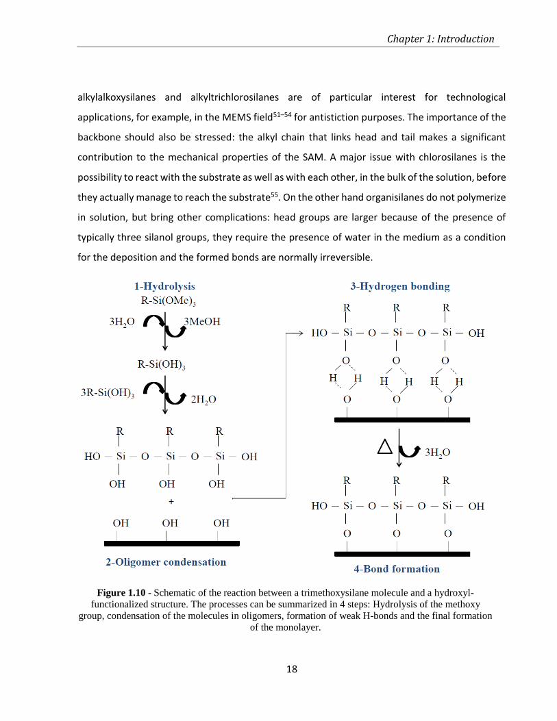
Figure 1.10 - Schematic of the reaction between a trimethoxysilane molecule and a hydroxyl-
functionalized structure. The processes can be summarized in 4 steps: Hydrolysis of the methoxy
group, condensation of the molecules in oligomers, formation of weak H-bonds and the final formation
of the monolayer.
Chapter 1: Introduction
19
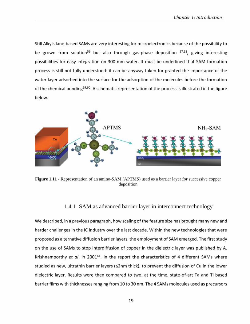
Still Alkylsilane-based SAMs are very interesting for microelectronics because of the possibility to
be grown from solution56 but also through gas-phase deposition 57,58, giving interesting
possibilities for easy integration on 300 mm wafer. It must be underlined that SAM formation
process is still not fully understood: it can be anyway taken for granted the importance of the
water layer adsorbed into the surface for the adsorption of the molecules before the formation
of the chemical bonding59,60. A schematic representation of the process is illustrated in the figure
below.
1.4.1 SAM as advanced barrier layer in interconnect technology
We described, in a previous paragraph, how scaling of the feature size has brought many new and
harder challenges in the IC industry over the last decade. Within the new technologies that were
proposed as alternative diffusion barrier layers, the employment of SAM emerged. The first study
on the use of SAMs to stop interdiffusion of copper in the dielectric layer was published by A.
Krishnamoorthy et al. in 200161. In the report the characteristics of 4 different SAMs where
studied as new, ultrathin barrier layers (≤2nm thick), to prevent the diffusion of Cu in the lower
dielectric layer. Results were then compared to two, at the time, state-of-art Ta and Ti based
barrier films with thicknesses ranging from 10 to 30 nm. The 4 SAMs molecules used as precursors
Figure 1.11 - Representation of an amino-SAM (APTMS) used as a barrier layer for successive copper
deposition
Chapter 1: Introduction
20
had different chain lengths and end groups, while the methoxysilane group, used to anchor the
molecule to the substrate remained unchanged. Conclusions were promising; it was established
that the inhibition effect of the diffusion of copper was caused by the presence of the SAM or, at
least, the time to failure was increased and the chain length and terminal group of the precursor
were able to modify these performances.
It should be noticed that until 2001 self-assembled monolayers were gaining interest in many
applications both in and out of the IC field (anticorrosion coatings, patterning, etc.)62, e.g., also in
2001, M.M. Sung et al. published a paper regarding the use of thiols on copper with similar
properties as the ones assembled on gold63. In 2003 Ramanath et al. compared some SAMs,
among which the one used by Krishnamoorthy et al., where) with the Ta/TaN conventional barrier
film, showing lower performance of the SAMs in terms of extrapolated mean-time to failure64.
MPTMS (containing a mercapto-, SH-, group) became used in the later years as a diffusion barrier
and as adhesion enhancer factor at the Cu/SiO2 interface65. New SAMs started to undergo through
testing: in 2004 Ganesan et al. utilized amino- and carboxy- terminated precursors for the same
purposes as before, assessing better behaviour for the latter66. First use of SAM barriers in IC-like
structure was shown by Gandhi et al. in 2007, who studied the effect of different monolayers in
single damascene structures67. Also, in a successive publication, Gandhi et al. demonstrated the
positive effect of curing the SAM at high temperature after deposition to increase adhesion
properties68.
Chapter 1: Introduction
21
It should be noticed that until 2008 no coupled characterization in terms of adhesion, process
stability and reliability and film properties were conducted. A publication by Caro et al., reported
the results of research conducted in imec laboratories about a screening made on precursors with
different head groups (methoxy-, chloro- or mixed) with different chain lengths and tail groups
(amino-, bromo-, ciano-, mercapto-, methen-). The paper concluded that different groups and
chain lengths could heavily modify the properties of the growing SAM, and that the amino-
terminated one, made by 3-APTMS (aminopropyltrimethoxysilane), was the most promising as an
inhibitor for Cu diffusion36,69. Since then many different papers, screening different SAMs, have
been successfully published. These studies have concluded that SAMs can be used as a barrier
layer, providing an interface toughening mechanism at copper/silica interfaces, tailored with
organosilanes. But SAMs have been proved useful not only as alternative barrier layers but also
for the improvement of copper deposition techniques like PVD, CVD and ElectroLess Deposition
(ELD).
In the last years imec research has gone towards the development of barrier properties of amino-
terminated groups, especially APTMS, resulting in publications70,71, along with the
implementation of these new deposition techniques, trying to solve PVD limitations. This is the
starting point of this research project36,72.
Figure 1.12 - Model of a Silane molecule: all the molecules in this group have in common the silicon
atom, uniting the hydrolysable groups and the backbone.
Chapter 1: Introduction
22
1.4.2 SAM deposition techniques
Several kinds of SAMs deposition processes have been studied since their discovery. Of all of them
especially the vapour-phase and liquid-phase deposition have been intensively used. Others, like
spraying or spin-coating, are sometimes used for special applications.
1.4.2.1 Liquid deposition
Probably the first deposition technique employed, liquid-phase assembled of organic molecules
is still the most widely used. It has been widely studied in the past three decades so the reaction
mechanism has been quite well understood. The liquid is very useful to provide an effective
medium to allow the SAMs precursors molecules to reach the substrate and react on and with it.
Different liquids can be used as deposition mediums other than water; organic solvents like
alcohols and toluene are largely used. An advantage of the wet process is the effectiveness at
room temperature, without need of vacuum formation. However it has been demonstrated that
the film quality can vary with the deposition temperature73. The technique suffers from
sensitiveness to humidity present in the ambient and polymerization of the precursor that may
create particulate over the surface55. Also the solvent has to be chosen wisely to avoid the
deposition of multilayers.
1.4.2.2 Vapour deposition
Vapour deposition has acquired interest in the recent past especially for industrial applications.
It represents a typical example of CVD, where the precursor is heated up at temperatures higher
than 100 °C. The SAM in a liquid phase is deposited in a reservoir and, once the temperature has
reached an optimal value, it evaporates, reaching the nearby substrate. Pressure is kept low: the
reaction chamber is normally kept near vacuum conditions and increases when the SAMs
Chapter 1: Introduction
23
precursor evaporates (vapour pressure around 5 torr). The process can be carried out at lower
temperatures (50-120 °C) if the reservoir consists of the SAM precursor diluted in a solution. Still
adequate vapour pressure of the precursor has to be reached to have a correct deposition.
Vapour deposition is useful in avoiding undesired side-reactions and favouring a monolayer
deposition. The mechanism of deposition is still not perfectly understood but studies have
confirmed that SAMs deposited with liquid and vapour process maintain comparable
properties74. The industrial interest in vapour deposition is justified by the previous cited
advantages over the liquid one but mainly because of the easier and less numerous process
phases. Liquid deposition involves a high number of rinsing and cleaning steps not necessary with
vapour deposition, making the latter very attractive under the scaling-up point of view.
1.5 Electroless Deposition (ELD)
Electroless deposition is a process that, although not recognized as such, has been used in practice
for centuries, even if only in the last 50 years important scientific results have been achieved75.
This became possible after the discovery of its working mechanisms by Dr. Abner Brenner and
Grace Riddel at the National Bureau of Standards, where they accidentally observed that the
additive H2PO2 caused apparent cathode efficiencies of more than 100% in a nickel electroplating
bath. This led them to the correct conclusion that some chemical reduction was involved. It is
defined as a nonelectrical plating of metals and plastics to achieve uniform coating by a process
of controlled autocatalytic (self-continuing) reduction. It involves deposition of many different
metals such as silver, gold, palladium, nickel, copper or alloys of these metals plus P or B by means
of a reducing chemical bath.
Chapter 1: Introduction
24
The name electroless can be somehow misleading. There are no external electrodes present in
the bath, so no external electric field is applied, but still there is transfer of charges (electric
current) involved. While in a typical electroplating process an anode connected to an external
power supply provides the metal ions necessary for the deposition, here the metal is supplied by
a metal salt dissolved in the bath. The cathodes role is instead taken on by the substrate while a
chemical reducing agent provides the electrons necessary for the reaction. A great advantage of
ELD over electroplating is due to the possibility to deposit metals even on nonconductive surface,
as well as metals and semiconductors.
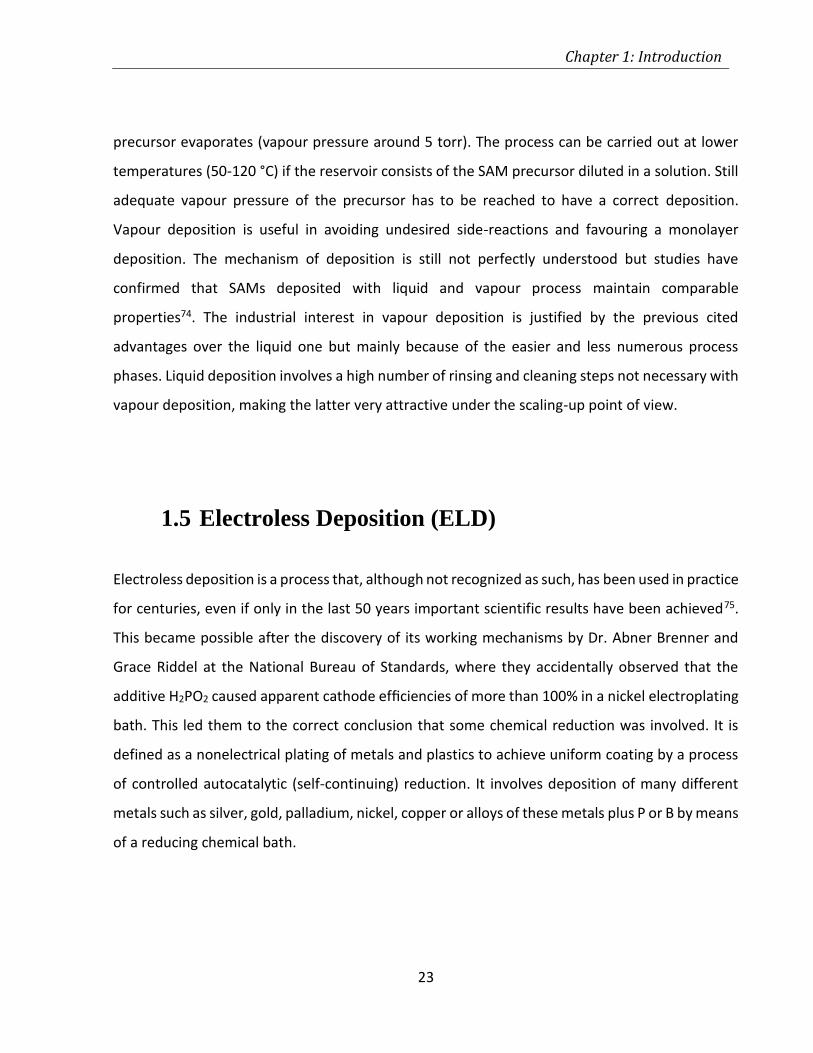
The process can be easily understood by looking at the schematized version in Fig 1.9.
The metal ion oxidizes on top of the substrate to form a metallic layer. This is possible thanks to
the electrons provided by the reducing agent made available due to the passage from a reduced
state to an oxidized one. In many cases the substrate is not able to catalyze the reaction. In this
Figure 1.13 - Electroless deposition process schematic. Up: the reaction is
catalyzed by the substrate. Down: the reaction is catalyzed by the deposited
metal.
Chapter 1: Introduction
25
case normally noble metal nanoparticles, already present on the substrate at the entering of the
ELD bath, are used to start the reaction. Once the reaction has started their role is no longer
important because it’s the same metal that catalyzes the reaction. This explains the autocatalytic
nature of the process.
A typical electroless solution is made by a blend of different chemicals, each of them performing
an important and exclusive function. This includes:
a source of metal ions
the reducing agent
complexing agents
stabilizers
inhibitors
energy
1.5.1 Metal Ions Source
As already said, metal ions come from a salt dissolved inside the solution. Most commonly used
salts belong to the sulphate family, like nickel and copper sulfates. The choice is due to the non-
deteriorating capabilities of the bath by the sulphate groups remaining in the bath after the
reduction of the metal on the surface. Other precursors include also metallorganic molecules
like nickel acetate or chloride compounds, used for more specific applications76.
1.5.2 Reducing Agents
The metals most commonly deposited by electroless deposition are shown in table 1.1, along with
commonly used reducing agents. Since the role of the reducing agent is to supply electrons, all
Chapter 1: Introduction
26
the listed species have similar structures in that they contain a certain number of reactive
hydrogen atoms. The catalytic dehydrogenation of the reducing agent is responsible for the metal
reduction.
Table 1.1 – Reducing agents commonly used in ELD processes.
Reducing agents for Electroless plating processes
Sodium Hypophosphite -
NaH2∙H2O Ni, Co, Cu, Pd, Ag
Sodium Borohydride - NaBH4 Ni, Au, Co, Cu, Ag
Dimethylamineborane -
(CH3)2NH∙BH3
Ni, Co, Cu, Ag, Au, Pd
Hydrazine - H2N∙NH2 Ni, Pd, Au
Formaldehyde - HCHO Cu, Ag
The metal deposition can then be understood as a sum of two electrochemical reactions (an
oxidation and a reduction) happening inside an electrochemical cell, with a consequential
liberation and consummation of electrons
The general reactions are:
Reduction of a metal ion
M+n + ne- → Mo
Oxidation of the reducing agent
Red → Ox + me-
Resulting in:
Chapter 1: Introduction
27
Overall Reaction
M+n + Red → Mo + Ox
The overall reaction can be derived through a simple sum of the two redox semi-reactions and
gives an idea of the stoichiometric reactions occurring during the metal deposition. However the
complexity of the reactions and of the other phenomena that take place inside the
electrochemical bath is much higher than the situation described by the chemical equations76.
Hence, it is necessary and convenient to study the mechanism occurring for the salt and reducing
agent we are interested in.
1.5.3 Complexing Agents
Over the decades many different additives to the plating bath have been developed. One family
is referred to as complexing agents. Formed mainly by organic acids or their salts (important
exceptions are the ammonium ion and pyrophosphate ion) they play three roles:
Help maintain a stable pH level
Prevent nickel salts precipitation
Reduce the presence of free metal ions77
The complexing agent acts by displacing the water molecules around the metal ion to form a
metal complex. The chemical properties of the metal ions in the aqueous solution are then
altered, affecting among many, the colour of the plating solution and most importantly the driving
force for the reduction76, as described by Nernst’s Law. The rate of the metal deposition is in
practice then proportional to the rate at which the metal-ligands bonds are broken and so
inversely proportional to the strength of the bonds. ELD is then described more effectively by
mixed potential and bath stability, while the reaction rate is heavily affected by the pH of the
bath78 because of its influence on the ∆E° of the reducing reaction79.
Chapter 1: Introduction
28
1.5.4 Additives
Under the name additives there are a high number of different compounds used in chemical baths
in order to increase the lifetime and stability of the solution.
Stabilizers are used in order to avoid a decomposition of the plating solution, which can happen
at any time. Decomposition comes normally along with an increase in the volume of hydrogen
gas evolved, that causes the formation of a fine black precipitate through the bulk of the solution
giving it a much darker colour. This precipitates are formed by metal salts, depending on the metal
plated and on the reducing agent used. Stabilizers are able to prevent or retard this homogenous
reaction, giving the possibility to use the bath for a long period, and in the meantime also
accelerate the plating process. Four “classes” are normally used as stabilizers:
Compounds based on IV group elements (Te, Se, etc.)
Unsaturated organic acids (maleic acid, etc.)
Heavy metal cations (Sn+2, Pb2+, etc.)
Compounds containing oxygen (AsO-2,MoO-2
4, etc.)
For a correct usage of stabilizers there must be a precise identification of the issues that can be
solved by the stabilizers. Secondly the compatibility of the stabilizers with the other chemicals
employed in the bath must be assessed: synergistic action with other additives could cause a loss
in catalytic activity. Finally the additives must not inhibit or lessen the effectiveness of the other
stabilizers present76,77.
Another family of additives is known as buffers. Buffers are substances used to avoid a relevant
change in pH towards more acidic or basic one. They normally act by reactions that consume or
reduce protons or hydrogen ions in the bulk of the solution or close to the plated surface. Better
is the buffer and higher must be the quantity of acid (or base) necessary to give the same change
Chapter 1: Introduction
29
in the pH of the bath. The maintenance of the pH of the deposition bath is essential because the
end-product film is strongly dependent on it.
Finally, surfactants are commonly used in ELD baths. H2 is a by-product that is always present
during electroless deposition and it has to be removed. By changing the surface energy,
surfactants are able to avoid H2 evolution or to favour the removal of it. The absence of H2
impurities inside the film is very beneficial to the film properties80.
Many other additives are still used in ELD solutions to give many different effects such as the
control of the surface tension, the removal of hydrogen from the deposits or the suppression of
its evolution, and the improvement of the quality of the metal film, etc76.
It is clear from this simple description of the typical compounds used in electroless deposition
processes that quality does not depend just on the plated metal. Physical properties such as
resistivity, roughness, hardness, adhesion, density of the film, etc. depend on many factors.
Temperature, pH, composition of the bath, catalytic actions of the substrate, but also additives
are among some these variables. The correlations lying between the quality of the film and the
type of the solution used are not scientifically understood. All the knowledge of the effect of the
bath chemistry on the film quality is mainly due to empirical works. An effective improvement in
the process efficiency and applicability is then very complicated. However the high level of control
of the morphology of the deposit can be exploited to give good filling of trenches up to
nanometres scale, essential for an effective use of the technique in the ultra-large scale
integration (ULSI) interconnect technology.
1.6 Nickel-Boron Electroless Deposition
This paragraph will be focusing on the electroless deposition of nickel boron alloys through an
explicit understanding of the reaction mechanisms governing the process, from a theoretical and
Chapter 1: Introduction
30
practical point of view. A good understanding of the reduction of the nickel ions through the
exploitation of the reactive reducing agent is essential to perform a correct development of the
process itself, by increasing the plating rate, the density and uniformity of the film and by
increasing the efficiency of the chemical species employed. In particular the possibility to have a
good control over the final composition of the layer in terms of boron content is of extreme
interest. The final boron content of the NiB deposit will have a large impact on defining the
properties of the alloy.
An initial step to understanding the mechanisms governing the NiB ELD is to underline some
essential features of the process:
Evolution of hydrogen is always present as a consequence of the reduction of the nickel
ions
Depending on the reducing agent employed, there will always be at least a second
element present in the deposition (boron, phosphorus)
The process of reduction has to take place on chosen substrate but also on the surface of
the depositing metal
Hydrogen is formed as a by-product of the reduction reaction
The molar ration of the deposited nickel with respect to the consumed reducing agent is
usually close to 1 or less.
The ratio of the utilized reducing agent is never close to 100%
The following section can then focus on the understanding of the chemical reactions governing
the NiB ELD as the properties of the formed layer and its possible applications.
The most important reducing agents containing boron are the borohydride ion (BH-4) and amine
boranes.
The borohydride reducing agent may consist of any water soluble borohydride compound but
sodium borohydride is generally preferred. Some disadvantages come from the usage of
borohydride based baths. In order to suppress the precipitation of nickel boride the pH has to be
Chapter 1: Introduction
31
kept above the value of 12. As a consequence it is necessary for the substrate to withstand such
basic environments.
Different possible mechanisms have been proposed: the accepted one, suggested by Mallory, on
the basis of experimental data81–83 is described in the following:
Reduction of nickel:
2𝑁𝑖+2 + 𝐵𝐻4− + 4𝐻2𝑂 → 2𝑁𝑖0 + 𝐵(𝑂𝐻)4
− + 2𝐻2 + 4𝐻+
Reduction of boron:
𝐵𝐻4− + 𝐻+ → 𝐵𝐻3 + 𝐻2 → 𝐵 + 5 2⁄ 𝐻2
Thus, the overall reaction is:
2𝑁𝑖+2 + 2𝐵𝐻4− + 4𝐻2𝑂 → 2𝑁𝑖0 + 𝐵 + 𝐵(𝑂𝐻)4
− + 92⁄ 𝐻2 + 3𝐻+
Commercial use of amine boranes has in general been limited to dimethylamineborane (DMAB),
(CH3)2NHBH3. While theoretically the three hydrogens bonded to the boron atom should be able
to reduce three nickel ions, this is not supported experimentally. Studies have confirmed that the
molar ratio of nickel ions reduced versus DMAB molecules consumed is approximately 1:182. As
before, we can write down the two semi-reactions.
Reduction of nickel:
3𝑁𝑖+2 + 2(𝐶𝐻3)2𝑁𝐻𝐵𝐻3 + 6𝐻2𝑂 → 3𝑁𝑖0 + 2(𝐶𝐻3)2𝑁𝐻2+ + 2𝐻3𝐵𝑂3 + 3𝐻2 + 4𝐻+
Reduction of boron:
(𝐶𝐻3)2𝑁𝐻𝐵𝐻3 + 𝐻+ → (𝐶𝐻3)2𝑁𝐻 + 𝐵𝐻3 + 𝐻+ → (𝐶𝐻3)2𝑁𝐻2+ + 𝐵 + 3
2⁄ 𝐻2
And, overall:
3𝑁𝑖+2 + 3(𝐶𝐻3)2𝑁𝐻𝐵𝐻3 + 6𝐻2𝑂 → 3𝑁𝑖0 + 𝐵 + 3(𝐶𝐻3)2𝑁𝐻2+ + 2𝐻3𝐵𝑂3 + 9
2⁄ 𝐻2 + 𝐻+
Chapter 1: Introduction
32
Concentration of boron in the film is mainly determined by the nature and concentration of the
introduced substances and also by the plating conditions. Normally the percentage of boron in
the NiB film is quite low, with nickel concentration range going from 90% to 99.9%, even if deposit
with 30% (or higher) of boron were also produced84–86.
As can be seen from the phase diagram the solubility of boron inside nickel is very low. Hence, for
low percentages of boron, the NiB layer would result in a metastable supersaturated alloy that
would separate creating a mixture of pure Ni and Ni3B. Experimentally it has been demonstrated
that for concentration of boron around 6% the deposit may have amorphous characteristics. Only
after anneal at 300-400 °C the film actually resembles more the thermodynamically stable
situation described by the phase diagram. Depending on the temperature and the heating
condition a mix of Ni3B and Ni2B is obtained87.
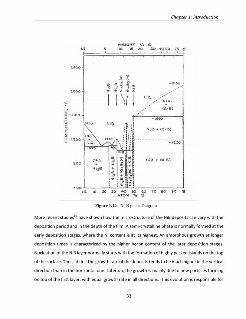
Chapter 1: Introduction
33
More recent studies88 have shown how the microstructure of the NiB deposits can vary with the
deposition period and in the depth of the film. A semi-crystalline phase is normally formed at the
early deposition stages, where the Ni content is at its highest. An amorphous growth at longer
deposition times is characterized by the higher boron content of the later deposition stages.
Nucleation of the NiB layer normally starts with the formation of highly packed islands on the top
of the surface. Thus, at first the growth rate of the deposits tends to be much higher in the vertical
direction than in the horizontal one. Later on, the growth is mainly due to new particles forming
on top of the first layer, with equal growth rate in all directions. This evolution is responsible for
Figure 1.14 - Ni-B phase Diagram
Chapter 1: Introduction
34
the change of morphology of the deposit, starting from a semi-crystalline columnar shape growth
to an amorphous one. The different growth modes can be responsible for the development of
tensile stresses inside the film. Consequently, atomic rearrangements can occur especially during
post-deposition anneal but also during prolonged deposition.
We described NiB ELD as an autocatalytic process, where the deposited metal is able to act as a
catalyser for a self-continuing reaction. It is anyway necessary for many substrates to be properly
activated, prior to the deposition step, in order for the deposition to occur. Some kinds of metals,
like Cu, Au, Ag, Pt, Pd are able to catalyse NiB deposition89, while others can be forced to act as a
catalytic surface by displacement plating of metals. For the other substrate, normally, palladium
metal is used as a catalyser centre and hence different technologies have been developed for its
deposition. Mainly Pd can be deposited with costly sputtering or PVD techniques or by immersion
of the substrate in solution containing palladium chloride90.
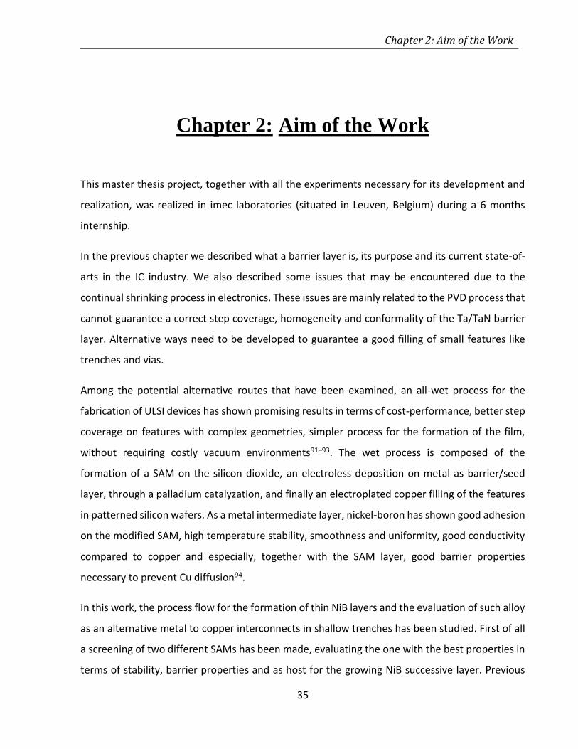
Chapter 2: Aim of the Work
35
Chapter 2: Aim of the Work
This master thesis project, together with all the experiments necessary for its development and
realization, was realized in imec laboratories (situated in Leuven, Belgium) during a 6 months
internship.
In the previous chapter we described what a barrier layer is, its purpose and its current state-of-
arts in the IC industry. We also described some issues that may be encountered due to the
continual shrinking process in electronics. These issues are mainly related to the PVD process that
cannot guarantee a correct step coverage, homogeneity and conformality of the Ta/TaN barrier
layer. Alternative ways need to be developed to guarantee a good filling of small features like
trenches and vias.
Among the potential alternative routes that have been examined, an all-wet process for the
fabrication of ULSI devices has shown promising results in terms of cost-performance, better step
coverage on features with complex geometries, simpler process for the formation of the film,
without requiring costly vacuum environments91–93. The wet process is composed of the
formation of a SAM on the silicon dioxide, an electroless deposition on metal as barrier/seed
layer, through a palladium catalyzation, and finally an electroplated copper filling of the features
in patterned silicon wafers. As a metal intermediate layer, nickel-boron has shown good adhesion
on the modified SAM, high temperature stability, smoothness and uniformity, good conductivity
compared to copper and especially, together with the SAM layer, good barrier properties
necessary to prevent Cu diffusion94.
In this work, the process flow for the formation of thin NiB layers and the evaluation of such alloy
as an alternative metal to copper interconnects in shallow trenches has been studied. First of all
a screening of two different SAMs has been made, evaluating the one with the best properties in
terms of stability, barrier properties and as host for the growing NiB successive layer. Previous
Chapter 2: Aim of the Work
36
studies have demonstrated how amino-terminated alkoxy-silanes are the most suitable as
precursors for this task36. The deposition relies in fact on the negatively charged amino groups
which are able to attract the positive Pd2+ charged atoms, present in the water-based PdCl2
solution used as catalyser, forming palladium clusters on the surface. Also the uptake of Pd and
Cl atoms from the SAM has been evaluated to assess the capability of the SAM to facilitate
successive depositions. So, if the first part is mainly dedicated to the evaluation of the goodness
of the SAM layers (but always paying attention to the successive deposition steps), the second
part will be mainly focusing on the metal deposit characteristics. Deposition of copper has been
thoroughly evaluated on SAM and in particular on amino-terminated SAM69,71,93. Some copper
issues, and more specifically diffusion, have been discussed in the introduction. Aware of these
issues, in this research, we tried an alternative route employing NiB not only as a barrier layer,
but also as a surrogate metal for line metallization. Two different NiB alloys have been evaluated,
with different percentages of boron.
Figure 2.1 - Schematic of the realized stack.
Chapter 2: Aim of the Work
37
The deposits will be considered acceptable if good results are achieved in terms of the following
characteristics: electrical (sheet and line resistance/resistivity), mechanical (adhesion) and
chemical (atomic percentages in the film). Also, the growth process will be analysed in order to
achieve a better understanding of the deposition process. The most significant measurements
have been made both on blanket and patterned wafer, cut in coupons of various dimensions, all
composed of silicon dioxide on silicon. The final stack, as can be seen in Fig. 2.1., is composed of
Si/SiO2/Amino-SAM/NiB-X%.
Chapter 3: Experimental Techniques
38
Chapter 3: Experimental techniques
3.1 SAMs deposition technique
All samples utilized during this research where used as substrates for SAM deposition. The
deposition could be realized using either a wet or a dry process, as later described. Several
different depositions where made, each varying one or more specifics of the process in order to
achieve the best SAM deposition technique for the subsequent ElecroLess Deposition (ELD) of
nickel-boron.
3.1.1 Vapour
The deposition of SAM using a vapour phase technique (PVD) was performed in a silanization
oven (Figure 3.1 – right). Unlike the wet deposition, SAMs PVD was realized on 300mm wafer
from which it was possible to cut out the coupons used in the following ELD experiments. In the
same fashion as the liquid deposition, the SiO2 substrate was precleaned in a Jealight UV-O3
cleaner (Figure 3.1 – left). This was performed in order to maximize the presence of –OH groups
on the surface of the wafer and remove contaminants that can be present on top of the wafer.
Atomic oxygen is simultaneously generated when molecular oxygen is dissociated by 184.9nm
and ozone by 253.7nm. The latter is also capable of remove most hydrocarbons (Figure 3.2). The
produced atomic oxygen is highly reactive: the exited carbon based contaminants on top of the
wafer are readily attacked by it, producing smaller and volatile compounds that desorb from the
surface, resulting in a perfectly clean substrate95.
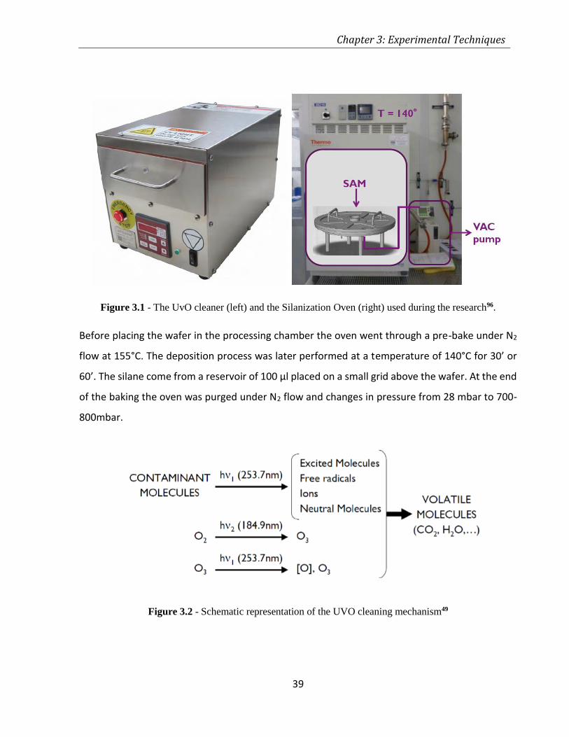
Chapter 3: Experimental Techniques
39
Figure 3.1 - The UvO cleaner (left) and the Silanization Oven (right) used during the research96.
Before placing the wafer in the processing chamber the oven went through a pre-bake under N2
flow at 155°C. The deposition process was later performed at a temperature of 140°C for 30’ or
60’. The silane come from a reservoir of 100 μl placed on a small grid above the wafer. At the end
of the baking the oven was purged under N2 flow and changes in pressure from 28 mbar to 700-
800mbar.
Figure 3.2 - Schematic representation of the UVO cleaning mechanism49
Chapter 3: Experimental Techniques
40
3.1.2 Liquid
Even if the resulting equilibrium structures should be and are, in fact, equivalent38, liquid
deposition is considered a better technique than the vapour one since it is more widely used and
the chemistry is better understood. Coupons cut from the Si wafer, with just a thin layer of SiO2
plasma obtained on top, were processed in the already described UV-O3 cleaner. The solution
used was based on methanol, with a SAM precursor concentration of 5 mM (365 μl on 250 ml of
solution). Also DIW was present (12.5 ml on a total of 250 ml) since H2O is essential for the
hydrolysis of silanes and their subsequent condensation. PEDA and DETA were both added in an
oxygen-free environment, inside a Glove Box, where oxygen concentration is lower than 10 ppm,
to avoid oxidation issues of the SAM precursor. Deposition is then carried out in tanks to avoid as
much as possible the entrance of moisture. Coupons have been kept inside the solution for a time
longer than 2 hours. This is the evaluated time needed to free a SAM from major defects. The
depositing methanol based solution, is optimal to obtain a monolayer film. The free energy of
the precursor molecule in the solution is such that the first deposition is energetically favoured,
but the deposition of the subsequent layers is not.
At the end of the deposition the coupons were rinsed to remove the last traces of solvent and
impurities. The step included 4 sonication processes for 2 minutes in respectively pure methanol,
acetone, ethanol and DIW. The increase in polarity of the baths guarantees an enhancement in
the solubility of the remaining previous solvent: the complete removal of it is essential to avoid
interference with the ELD experiments, performed in aqueous solutions.
3.2 Contact angle
The measurement of the contact angle is a rather simple yet fast method to evaluate the wetting
properties of surfaces through the use of a solvent droplet, typically water. The Dataphysics
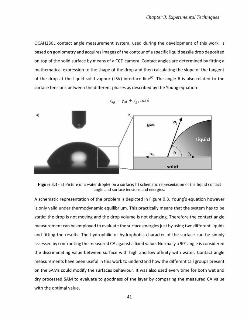
Chapter 3: Experimental Techniques
41
OCAH230L contact angle measurement system, used during the development of this work, is
based on goniometry and acquires images of the contour of a specific liquid sessile drop deposited
on top of the solid surface by means of a CCD camera. Contact angles are determined by fitting a
mathematical expression to the shape of the drop and then calculating the slope of the tangent
of the drop at the liquid-solid-vapour (LSV) interface line97. The angle θ is also related to the
surface tensions between the different phases as described by the Young equation:
𝛾𝑠𝑔 = 𝛾𝑠𝑙 + 𝛾𝑔𝑠𝑐𝑜𝑠𝜗
Figure 3.3 - a) Picture of a water droplet on a surface; b) schematic representation of the liquid contact
angle and surface tensions and energies.
A schematic representation of the problem is depicted in Figure 9.3. Young’s equation however
is only valid under thermodynamic equilibrium. This practically means that the system has to be
static: the drop is not moving and the drop volume is not changing. Therefore the contact angle
measurement can be employed to evaluate the surface energies just by using two different liquids
and fitting the results. The hydrophilic or hydrophobic character of the surface can be simply
assessed by confronting the measured CA against a fixed value. Normally a 90° angle is considered
the discriminating value between surface with high and low affinity with water. Contact angle
measurements have been useful in this work to understand how the different tail groups present
on the SAMs could modify the surfaces behaviour. It was also used every time for both wet and
dry processed SAM to evaluate to goodness of the layer by comparing the measured CA value
with the optimal value.
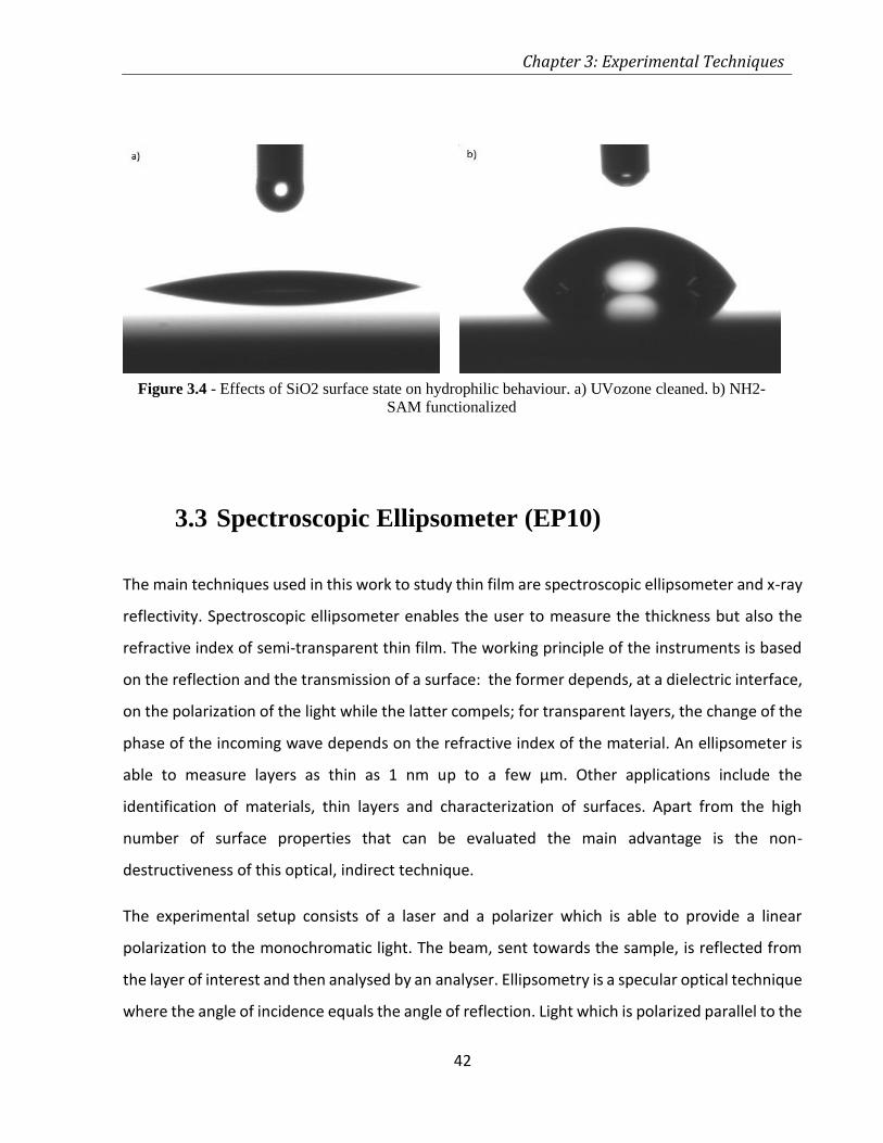
Chapter 3: Experimental Techniques
42
3.3 Spectroscopic Ellipsometer (EP10)
The main techniques used in this work to study thin film are spectroscopic ellipsometer and x-ray
reflectivity. Spectroscopic ellipsometer enables the user to measure the thickness but also the
refractive index of semi-transparent thin film. The working principle of the instruments is based
on the reflection and the transmission of a surface: the former depends, at a dielectric interface,
on the polarization of the light while the latter compels; for transparent layers, the change of the
phase of the incoming wave depends on the refractive index of the material. An ellipsometer is
able to measure layers as thin as 1 nm up to a few μm. Other applications include the
identification of materials, thin layers and characterization of surfaces. Apart from the high
number of surface properties that can be evaluated the main advantage is the non-
destructiveness of this optical, indirect technique.
The experimental setup consists of a laser and a polarizer which is able to provide a linear
polarization to the monochromatic light. The beam, sent towards the sample, is reflected from
the layer of interest and then analysed by an analyser. Ellipsometry is a specular optical technique
where the angle of incidence equals the angle of reflection. Light which is polarized parallel to the
Figure 3.4 - Effects of SiO2 surface state on hydrophilic behaviour. a) UVozone cleaned. b) NH2-
SAM functionalized
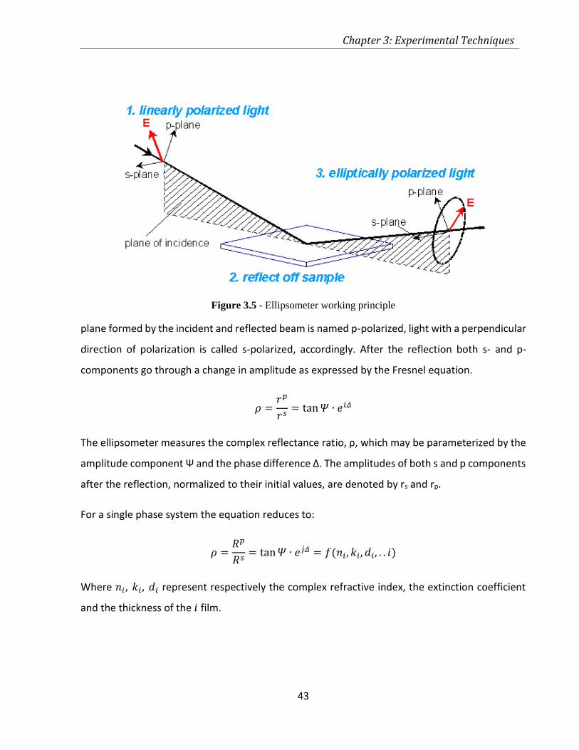
Chapter 3: Experimental Techniques
43
plane formed by the incident and reflected beam is named p-polarized, light with a perpendicular
direction of polarization is called s-polarized, accordingly. After the reflection both s- and p-
components go through a change in amplitude as expressed by the Fresnel equation.
𝜌 =𝑟𝑝
𝑟𝑠= tan 𝛹 ∙ 𝑒𝑖𝛥
The ellipsometer measures the complex reflectance ratio, ρ, which may be parameterized by the
amplitude component Ψ and the phase difference Δ. The amplitudes of both s and p components
after the reflection, normalized to their initial values, are denoted by rs and rp.
For a single phase system the equation reduces to:
𝜌 =𝑅𝑝
𝑅𝑠= tan 𝛹 ∙ 𝑒𝑗𝛥 = 𝑓(𝑛𝑖, 𝑘𝑖 , 𝑑𝑖, . . 𝑖)
Where 𝑛𝑖 , 𝑘𝑖 , 𝑑𝑖 represent respectively the complex refractive index, the extinction coefficient
and the thickness of the 𝑖 film.
Figure 3.5 - Ellipsometer working principle
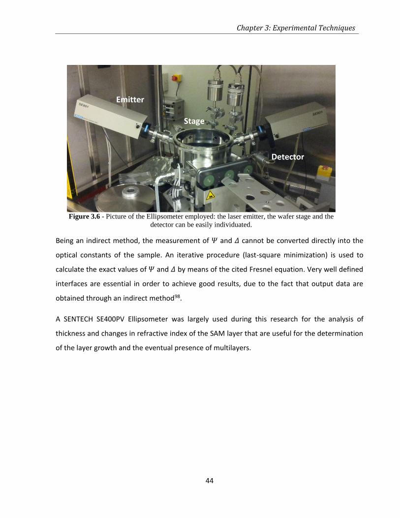
Chapter 3: Experimental Techniques
44
Being an indirect method, the measurement of 𝛹 and 𝛥 cannot be converted directly into the
optical constants of the sample. An iterative procedure (last-square minimization) is used to
calculate the exact values of 𝛹 and 𝛥 by means of the cited Fresnel equation. Very well defined
interfaces are essential in order to achieve good results, due to the fact that output data are
obtained through an indirect method98.
A SENTECH SE400PV Ellipsometer was largely used during this research for the analysis of
thickness and changes in refractive index of the SAM layer that are useful for the determination
of the layer growth and the eventual presence of multilayers.
Figure 3.6 - Picture of the Ellipsometer employed: the laser emitter, the wafer stage and the
detector can be easily individuated.
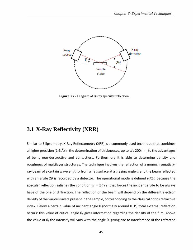
Chapter 3: Experimental Techniques
45
3.1 X-Ray Reflectivity (XRR)
Similar to Ellipsometry, X-Ray Reflectometry (XRR) is a commonly used technique that combines
a higher precision (1-3 Å) in the determination of thicknesses, up to c/a 200 nm, to the advantages
of being non-destructive and contactless. Furthermore it is able to determine density and
roughness of multilayer structures. The technique involves the reflection of a monochromatic x-
ray beam of a certain wavelength λ from a flat surface at a grazing angle ω and the beam reflected
with an angle 2θ is recorded by a detector. The operational mode is defined 𝜗/2𝜗 because the
specular reflection satisfies the condition 𝜔 = 2𝜗/2, that forces the incident angle to be always
have of the one of diffraction. The reflection of the beam will depend on the different electron
density of the various layers present in the sample, corresponding to the classical optics refractive
index. Below a certain value of incident angle θ (normally around 0.3°) total external reflection
occurs: this value of critical angle θc gives information regarding the density of the film. Above
the value of θc the intensity will vary with the angle θ, giving rise to interference of the refracted
Figure 3.7 - Diagram of X-ray specular reflection.
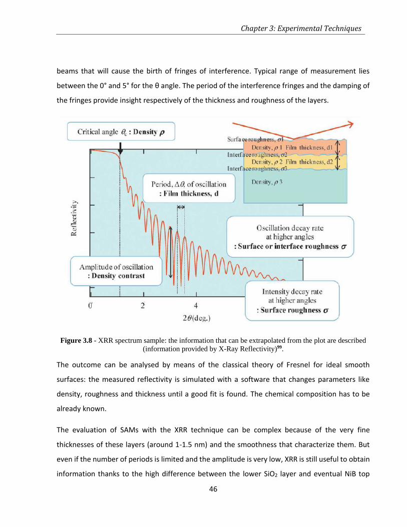
Chapter 3: Experimental Techniques
46
beams that will cause the birth of fringes of interference. Typical range of measurement lies
between the 0° and 5° for the θ angle. The period of the interference fringes and the damping of
the fringes provide insight respectively of the thickness and roughness of the layers.
Figure 3.8 - XRR spectrum sample: the information that can be extrapolated from the plot are described
(information provided by X-Ray Reflectivity)99.
The outcome can be analysed by means of the classical theory of Fresnel for ideal smooth
surfaces: the measured reflectivity is simulated with a software that changes parameters like
density, roughness and thickness until a good fit is found. The chemical composition has to be
already known.
The evaluation of SAMs with the XRR technique can be complex because of the very fine
thicknesses of these layers (around 1-1.5 nm) and the smoothness that characterize them. But
even if the number of periods is limited and the amplitude is very low, XRR is still useful to obtain
information thanks to the high difference between the lower SiO2 layer and eventual NiB top
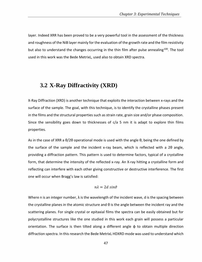
Chapter 3: Experimental Techniques
47
layer. Indeed XRR has been proved to be a very powerful tool in the assessment of the thickness
and roughness of the NiB layer mainly for the evaluation of the growth rate and the film resistivity
but also to understand the changes occurring in the thin film after pulse annealing100. The tool
used in this work was the Bede MetrixL, used also to obtain XRD spectra.
3.2 X-Ray Diffractivity (XRD)
X-Ray Diffraction (XRD) is another technique that exploits the interaction between x-rays and the
surface of the sample. The goal, with this technique, is to identify the crystalline phases present
in the films and the structural properties such as strain rate, grain size and/or phase composition.
Since the sensibility goes down to thicknesses of c/a 5 nm it is adapt to explore thin films
properties.
As in the case of XRR a θ/2θ operational mode is used with the angle θ, being the one defined by
the surface of the sample and the incident x-ray beam, which is reflected with a 2θ angle,
providing a diffraction pattern. This pattern is used to determine factors, typical of a crystalline
form, that determine the intensity of the reflected x-ray. An X-ray hitting a crystalline form and
reflecting can interfere with each other giving constructive or destructive interference. The first
one will occur when Bragg’s law is satisfied:
𝑛𝜆 = 2𝑑 𝑠𝑖𝑛𝜗
Where n is an integer number, λ is the wavelength of the incident wave, d is the spacing between
the crystalline planes in the atomic structure and θ is the angle between the incident ray and the
scattering planes. For single crystal or epitaxial films the spectra can be easily obtained but for
polycrystalline structures like the one studied in this work each grain will possess a particular
orientation. The surface is then tilted along a different angle φ to obtain multiple direction
diffraction spectra. In this research the Bede MetrixL HDXRD mode was used to understand which
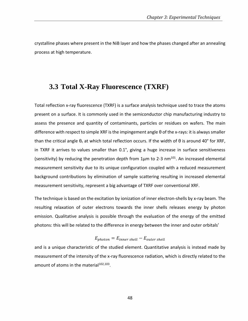
Chapter 3: Experimental Techniques
48
crystalline phases where present in the NiB layer and how the phases changed after an annealing
process at high temperature.
3.3 Total X-Ray Fluorescence (TXRF)
Total reflection x-ray fluorescence (TXRF) is a surface analysis technique used to trace the atoms
present on a surface. It is commonly used in the semiconductor chip manufacturing industry to
assess the presence and quantity of contaminants, particles or residues on wafers. The main
difference with respect to simple XRF is the impingement angle θ of the x-rays: it is always smaller
than the critical angle θc at which total reflection occurs. If the width of θ is around 40° for XRF,
in TXRF it arrives to values smaller than 0.1°, giving a huge increase in surface sensitiveness
(sensitivity) by reducing the penetration depth from 1μm to 2-3 nm101. An increased elemental
measurement sensitivity due to its unique configuration coupled with a reduced measurement
background contributions by elimination of sample scattering resulting in increased elemental
measurement sensitivity, represent a big advantage of TXRF over conventional XRF.
The technique is based on the excitation by ionization of inner electron-shells by x-ray beam. The
resulting relaxation of outer electrons towards the inner shells releases energy by photon
emission. Qualitative analysis is possible through the evaluation of the energy of the emitted
photons: this will be related to the difference in energy between the inner and outer orbitals’
𝐸𝑝ℎ𝑜𝑡𝑜𝑛 = 𝐸𝑖𝑛𝑛𝑒𝑟 𝑠ℎ𝑒𝑙𝑙 − 𝐸𝑜𝑢𝑡𝑒𝑟 𝑠ℎ𝑒𝑙𝑙
and is a unique characteristic of the studied element. Quantitative analysis is instead made by
measurement of the intensity of the x-ray fluorescence radiation, which is directly related to the
amount of atoms in the material102,103.
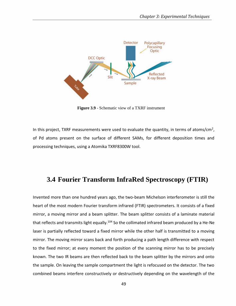
Chapter 3: Experimental Techniques
49
In this project, TXRF measurements were used to evaluate the quantity, in terms of atoms/cm2,
of Pd atoms present on the surface of different SAMs, for different deposition times and
processing techniques, using a Atomika TXRF8300W tool.
3.4 Fourier Transform InfraRed Spectroscopy (FTIR)
Invented more than one hundred years ago, the two-beam Michelson interferometer is still the
heart of the most modern Fourier transform infrared (FTIR) spectrometers. It consists of a fixed
mirror, a moving mirror and a beam splitter. The beam splitter consists of a laminate material
that reflects and transmits light equally.104 So the collimated infrared beam produced by a He-Ne
laser is partially reflected toward a fixed mirror while the other half is transmitted to a moving
mirror. The moving mirror scans back and forth producing a path length difference with respect
to the fixed mirror; at every moment the position of the scanning mirror has to be precisely
known. The two IR beams are then reflected back to the beam splitter by the mirrors and onto
the sample. On leaving the sample compartment the light is refocused on the detector. The two
combined beams interfere constructively or destructively depending on the wavelength of the
Figure 3.9 - Schematic view of a TXRF instrument
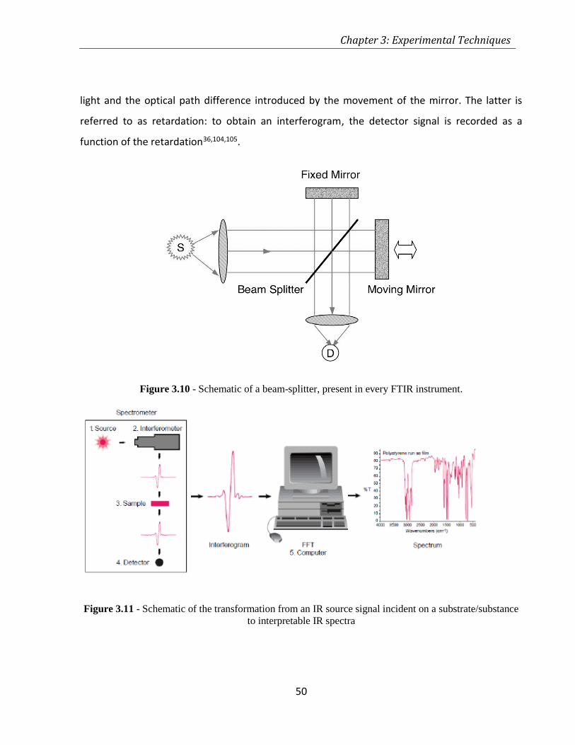
Chapter 3: Experimental Techniques
50
light and the optical path difference introduced by the movement of the mirror. The latter is
referred to as retardation: to obtain an interferogram, the detector signal is recorded as a
function of the retardation36,104,105.
Figure 3.10 - Schematic of a beam-splitter, present in every FTIR instrument.
Figure 3.11 - Schematic of the transformation from an IR source signal incident on a substrate/substance
to interpretable IR spectra
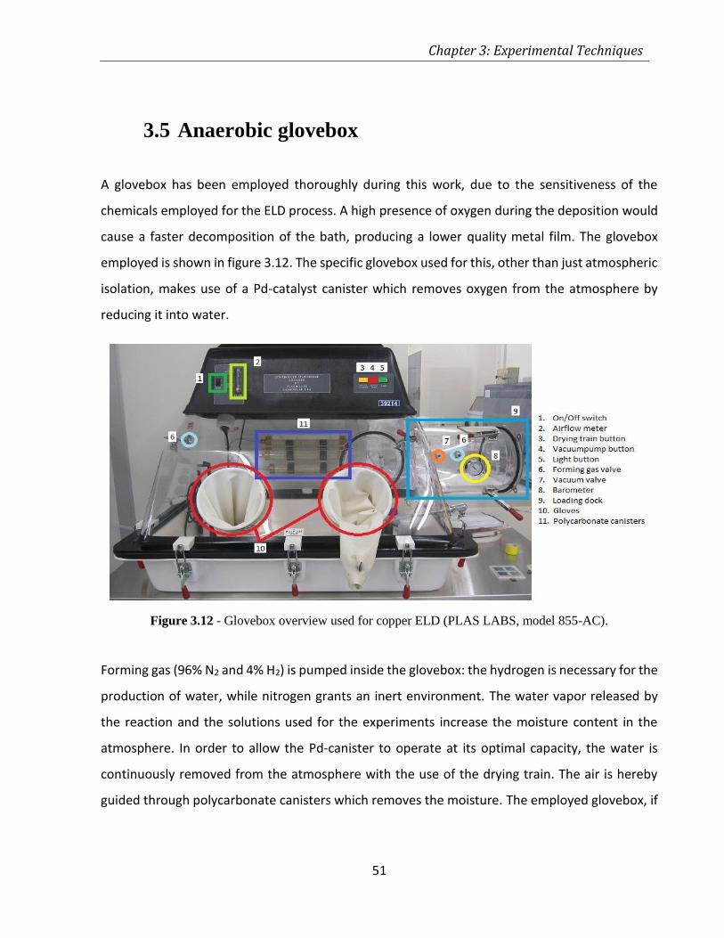
Chapter 3: Experimental Techniques
51
3.5 Anaerobic glovebox
A glovebox has been employed thoroughly during this work, due to the sensitiveness of the
chemicals employed for the ELD process. A high presence of oxygen during the deposition would
cause a faster decomposition of the bath, producing a lower quality metal film. The glovebox
employed is shown in figure 3.12. The specific glovebox used for this, other than just atmospheric
isolation, makes use of a Pd-catalyst canister which removes oxygen from the atmosphere by
reducing it into water.
Forming gas (96% N2 and 4% H2) is pumped inside the glovebox: the hydrogen is necessary for the
production of water, while nitrogen grants an inert environment. The water vapor released by
the reaction and the solutions used for the experiments increase the moisture content in the
atmosphere. In order to allow the Pd-canister to operate at its optimal capacity, the water is
continuously removed from the atmosphere with the use of the drying train. The air is hereby
guided through polycarbonate canisters which removes the moisture. The employed glovebox, if
Figure 3.12 - Glovebox overview used for copper ELD (PLAS LABS, model 855-AC).
Chapter 3: Experimental Techniques
52
used correctly, grants an atmosphere practically free from O2 (concentration of the order of a
fraction of ppm).
3.6 X-Ray Photoelectron Spectroscopy (XPS)
X-ray Photoelectron Spectroscopy (XPS), also known as ESCA (Electron Spectroscopy for Chemical
Analysis) is a technique mostly used to retrieve chemical state of elements at the surface. As most
of the surface analysis technique it uses a focused beam of x-rays aimed towards the surface of
the samples to obtain a spectrum while the kinetic energy and number of electrons that escape
from the top (from 0 to c/a 10 nm) of the material being analysed.
In a simple XPS experiment a X-ray beam illuminates a sample from which electrons are ejected
as a result of the photoelectric effect. The kinetic energy of the ejected electrons is then
determined by an electron analyser. As the energies of the X-ray and of the ejected electron are
known, the binding energy of the electron can be determined:
𝐸𝑏𝑖𝑛𝑑𝑖𝑛𝑔 = 𝐸𝑝ℎ𝑜𝑡𝑜𝑛 − (𝐸𝑘𝑖𝑛𝑡𝑒𝑖𝑐 + φ)
where Ebinding is the binding energy (BE) of the electron, Ephoton is the energy of the X-ray photons
being used, Ekinetic is the kinetic energy of the electron as measured by the instrument and φ is
the work function of the spectrometer (not the material). The work function term φ is essentially
an instrumental correction factor that accounts for the few eV of energy given up by the
photoelectron as it becomes absorbed by the instrument's detector. The equation above simply
takes into account the conservation of energy of the electron during the process. Knowing the
binding energy leads to an easy identification of the elements from which the electron originates.
Depending on the chemical state of the elements, small variations of the binding energy may be
present leading to chemical analysis. IMEC has a Theta300 system from Thermo Instruments: it is
equipped with a monochromatized Al Ka X-ray source (1486.6 eV), a neutralization gun and a
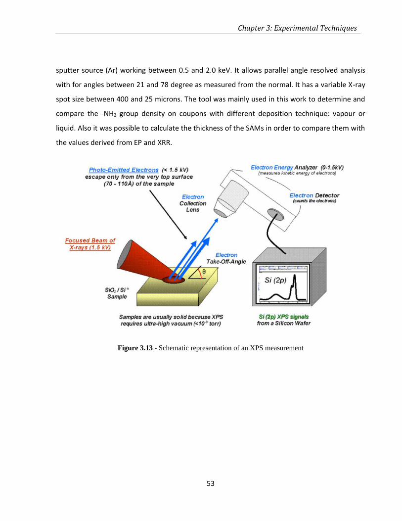
Chapter 3: Experimental Techniques
53
sputter source (Ar) working between 0.5 and 2.0 keV. It allows parallel angle resolved analysis
with for angles between 21 and 78 degree as measured from the normal. It has a variable X-ray
spot size between 400 and 25 microns. The tool was mainly used in this work to determine and
compare the -NH2 group density on coupons with different deposition technique: vapour or
liquid. Also it was possible to calculate the thickness of the SAMs in order to compare them with
the values derived from EP and XRR.
Figure 3.13 - Schematic representation of an XPS measurement
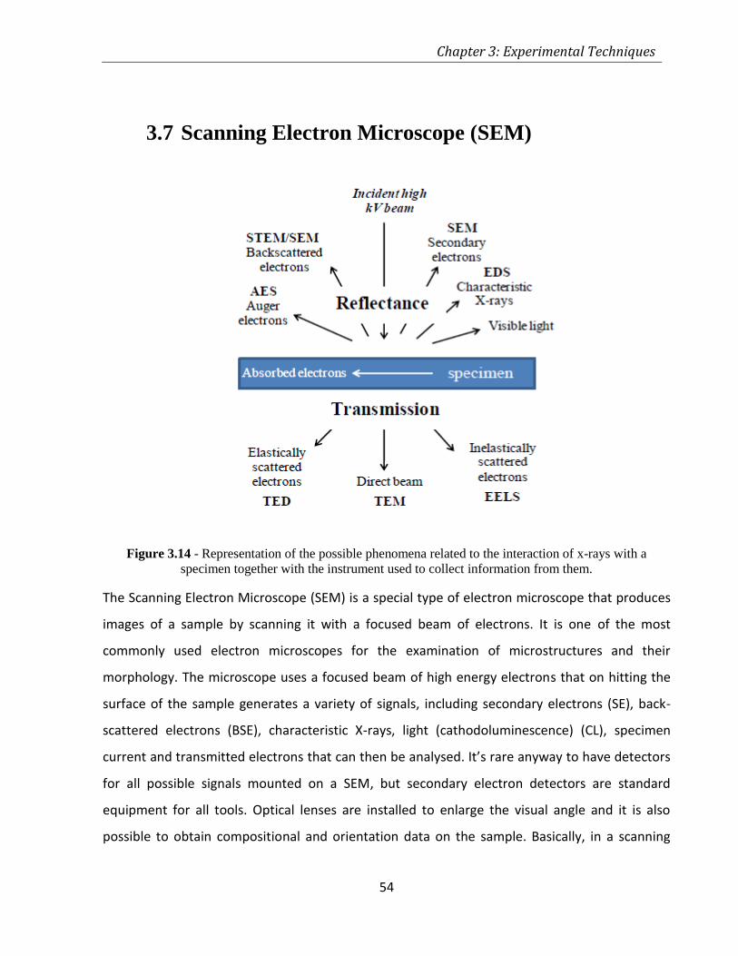
Chapter 3: Experimental Techniques
54
3.7 Scanning Electron Microscope (SEM)
Figure 3.14 - Representation of the possible phenomena related to the interaction of x-rays with a
specimen together with the instrument used to collect information from them.
The Scanning Electron Microscope (SEM) is a special type of electron microscope that produces
images of a sample by scanning it with a focused beam of electrons. It is one of the most
commonly used electron microscopes for the examination of microstructures and their
morphology. The microscope uses a focused beam of high energy electrons that on hitting the
surface of the sample generates a variety of signals, including secondary electrons (SE), back-
scattered electrons (BSE), characteristic X-rays, light (cathodoluminescence) (CL), specimen
current and transmitted electrons that can then be analysed. It’s rare anyway to have detectors
for all possible signals mounted on a SEM, but secondary electron detectors are standard
equipment for all tools. Optical lenses are installed to enlarge the visual angle and it is also
possible to obtain compositional and orientation data on the sample. Basically, in a scanning
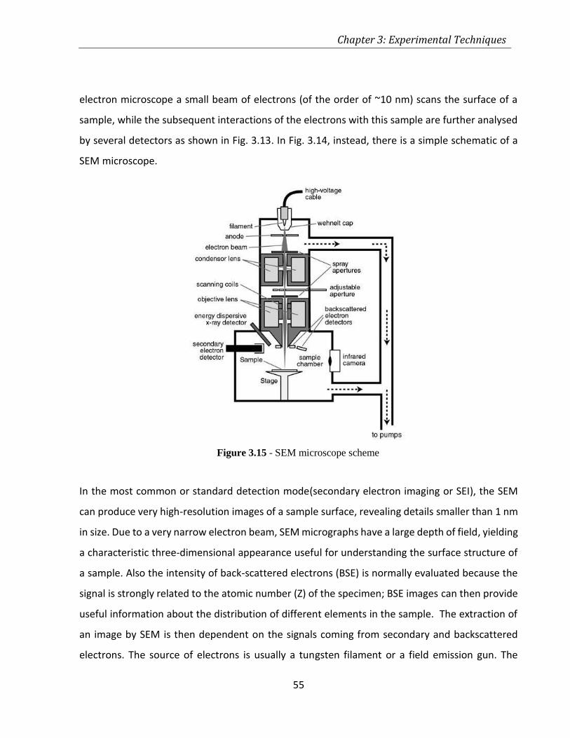
Chapter 3: Experimental Techniques
55
electron microscope a small beam of electrons (of the order of ~10 nm) scans the surface of a
sample, while the subsequent interactions of the electrons with this sample are further analysed
by several detectors as shown in Fig. 3.13. In Fig. 3.14, instead, there is a simple schematic of a
SEM microscope.
In the most common or standard detection mode(secondary electron imaging or SEI), the SEM
can produce very high-resolution images of a sample surface, revealing details smaller than 1 nm
in size. Due to a very narrow electron beam, SEM micrographs have a large depth of field, yielding
a characteristic three-dimensional appearance useful for understanding the surface structure of
a sample. Also the intensity of back-scattered electrons (BSE) is normally evaluated because the
signal is strongly related to the atomic number (Z) of the specimen; BSE images can then provide
useful information about the distribution of different elements in the sample. The extraction of
an image by SEM is then dependent on the signals coming from secondary and backscattered
electrons. The source of electrons is usually a tungsten filament or a field emission gun. The
Figure 3.15 - SEM microscope scheme
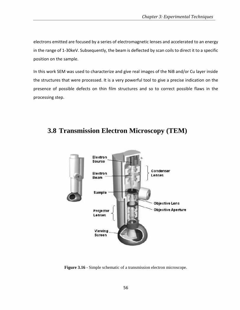
Chapter 3: Experimental Techniques
56
electrons emitted are focused by a series of electromagnetic lenses and accelerated to an energy
in the range of 1-30keV. Subsequently, the beam is deflected by scan coils to direct it to a specific
position on the sample.
In this work SEM was used to characterize and give real images of the NiB and/or Cu layer inside
the structures that were processed. It is a very powerful tool to give a precise indication on the
presence of possible defects on thin film structures and so to correct possible flaws in the
processing step.
3.8 Transmission Electron Microscopy (TEM)
Figure 3.16 - Simple schematic of a transmission electron microscope.
Chapter 3: Experimental Techniques
57
The Transmission Electron Microscopy (TEM) (schematic in figure above) is a microscopy
technique where a high energy monochromatic and coherent beam of electrons is transmitted
through an ultra-thin specimen (less than 200 nm), interacting with the latter as it passes through
it. These electrons are scattered at different angles depending on the density of the atoms
encountered. One of the most important advantages of TEM over other characterization
techniques is that information can be obtained both from direct and indirect space. In direct
space, two modes are typical, i.e. TEM and High resolution TEM (HRTEM) which can discern the
structure and morphology of a material thanks to the high magnification and high resolution
allowed by this technique. In indirect space, diffraction yields information on the crystallinity of
the specimen. Besides these possibilities, chemical information can also be acquired using the
inelastic interaction of the incoming electrons with the atoms of the specimen. Here two
techniques are typical, i.e. electron energy loss spectroscopy (EELS), and energy dispersive X-ray
spectroscopy (EDS).
For the aim of imaging the filling of the trenches in patterned coupons with the NiB or Cu layer,
and assessing the interdiffusion of chemical metals inside the silicon or the dissolution of barrier
layers inside the metals, TEM has been an extremely important tool. On the other hand, despite
the huge potential of the microscope, the imaging of the SAM layer still remains a great challenge.
In this work it has been impossible to distinguish the SAM layer from the native SiO2 or the MnNx
barrier layer.
3.9 Four Point Probe
During the realization of this project two different “4 point probe” tools for the evaluation of
resistance were used. In particular, while the basic principles on which the tools worked were the
same, the setup was different, one allowing a best usage for thin films, and the other for line
resistivity. The 4 point probe uses separate pairs of current-carrying and voltage-sensing
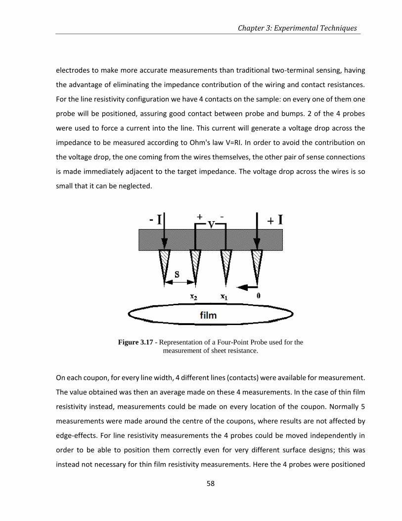
Chapter 3: Experimental Techniques
58
electrodes to make more accurate measurements than traditional two-terminal sensing, having
the advantage of eliminating the impedance contribution of the wiring and contact resistances.
For the line resistivity configuration we have 4 contacts on the sample: on every one of them one
probe will be positioned, assuring good contact between probe and bumps. 2 of the 4 probes
were used to force a current into the line. This current will generate a voltage drop across the
impedance to be measured according to Ohm's law V=RI. In order to avoid the contribution on
the voltage drop, the one coming from the wires themselves, the other pair of sense connections
is made immediately adjacent to the target impedance. The voltage drop across the wires is so
small that it can be neglected.
On each coupon, for every line width, 4 different lines (contacts) were available for measurement.
The value obtained was then an average made on these 4 measurements. In the case of thin film
resistivity instead, measurements could be made on every location of the coupon. Normally 5
measurements were made around the centre of the coupons, where results are not affected by
edge-effects. For line resistivity measurements the 4 probes could be moved independently in
order to be able to position them correctly even for very different surface designs; this was
instead not necessary for thin film resistivity measurements. Here the 4 probes were positioned
Figure 3.17 - Representation of a Four-Point Probe used for the
measurement of sheet resistance.
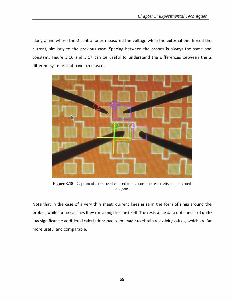
Chapter 3: Experimental Techniques
59
along a line where the 2 central ones measured the voltage while the external one forced the
current, similarly to the previous case. Spacing between the probes is always the same and
constant. Figure 3.16 and 3.17 can be useful to understand the differences between the 2
different systems that have been used.
Note that in the case of a very thin sheet, current lines arise in the form of rings around the
probes, while for metal lines they run along the line itself. The resistance data obtained is of quite
low significance: additional calculations had to be made to obtain resistivity values, which are far
more useful and comparable.
Figure 3.18 - Caption of the 4 needles used to measure the resistivity on patterned
coupons.
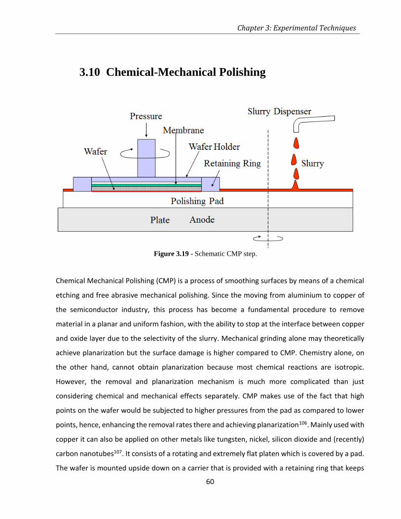
Chapter 3: Experimental Techniques
60
3.10 Chemical-Mechanical Polishing
Chemical Mechanical Polishing (CMP) is a process of smoothing surfaces by means of a chemical
etching and free abrasive mechanical polishing. Since the moving from aluminium to copper of
the semiconductor industry, this process has become a fundamental procedure to remove
material in a planar and uniform fashion, with the ability to stop at the interface between copper
and oxide layer due to the selectivity of the slurry. Mechanical grinding alone may theoretically
achieve planarization but the surface damage is higher compared to CMP. Chemistry alone, on
the other hand, cannot obtain planarization because most chemical reactions are isotropic.
However, the removal and planarization mechanism is much more complicated than just
considering chemical and mechanical effects separately. CMP makes use of the fact that high
points on the wafer would be subjected to higher pressures from the pad as compared to lower
points, hence, enhancing the removal rates there and achieving planarization106. Mainly used with
copper it can also be applied on other metals like tungsten, nickel, silicon dioxide and (recently)
carbon nanotubes107. It consists of a rotating and extremely flat platen which is covered by a pad.
The wafer is mounted upside down on a carrier that is provided with a retaining ring that keeps
Figure 3.19 - Schematic CMP step.
Chapter 3: Experimental Techniques
61
the wafer in the correct horizontal position and vacuum is used to keep the wafer in the carrier
during loading and unloading. Good speed control is important to prevent damage to the polished
layer i.e. cracking or delamination; both, the platen and the carrier, are rotating and speed can
be easily controlled. During chemical mechanical polishing, pressure is applied by a downward
force transferred to the carrier through its axis and a gimbal mechanism108.
In this work an experimental Mecapol polisher was used to remove the extra NiB on patterned
coupons in order to measure the line resistivity. Different pads are available on the tool (for
wafers from 2 to 8 inches and for wafer pieces), but for 2.9x2.6 cm coupons we used one type
with precise pressure content. It was possible to adjust the rotating speed of the pad and the
holder as well as the pressure of the pad to get the best result without damaging the metal or
polishing the oxide surface109. Two different commercial slurries were used on NiB 1% and NiB
10% layers: ACUPLANE 4100 and ACUPLANE 6000 A0. The first one gave the best results for both
NiB chemistries because of its good selectivity between metal and SiO2 and ability to uniformly
polish the NiB layer.
Chapter 4: Self-Assembled Monolayer Characterization
62
Chapter 4: Self-Assembled Monolayer
Characterization
This chapter will be focusing on the presentation of the experiments realized for the
characterization of the two studied SAM layers. This was possible through the evaluation of some
important physical and chemical properties of the organic film, considering different precursors,
deposition procedures and methods.
4.1 Introduction
During the development of this work two different molecules, employed as precursors for the
SAM formation, where intensively studied. The precursors differed from each other in the
number of amino-groups and in the kind of backbone uniting tail and head groups.
(Aminoethylaminomethyl)-phenylethyltrimethoxysilane (PEDA) is characterized by two amino
groups and a bulky, aromatic group, which is known to enhance the barrier properties of the SAM
layer61; (3-Trimethoxysilylpropyl)-diethylenetriamine (DETA) shows instead a higher number of
amino-group, with an alkyl-based backbone (Table 4.1). While DETA was studied for the first time
in this kind of applications; PEDA has already shown promising results in previous studies and has
been employed for further analysis other than as benchmark. Both SAMs belong to the -
trimethoxysilane group (–Si(OCH3)3). The -trichlorosilane (–SiCl3) based SAM show very good
barrier properties when coupled with Cu, up to 400 °C, with no silicides formation. On the
contrary more reactive groups, like –SH and –C5H4N, present lower thermal stability (200-300 °C).
Also the –trimethoxysilane group shows low thermal stability and silicides formation at low
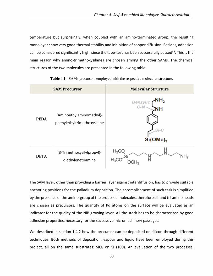
Chapter 4: Self-Assembled Monolayer Characterization
63
temperature but surprisingly, when coupled with an amino-terminated group, the resulting
monolayer show very good thermal stability and inhibition of copper diffusion. Besides, adhesion
can be considered significantly high, since the tape-test has been successfully passed36. This is the
main reason why amino-trimethoxysilanes are chosen among the other SAMs. The chemical
structures of the two molecules are presented in the following table.
Table 4.1 - SAMs precursors employed with the respective molecular structure.
SAM Precursor Molecular Structure
PEDA (Aminoethylaminomethyl)-
phenylethyltrimethoxysilane
DETA (3-Trimethoxysilylpropyl)-
diethylenetriamine
The SAM layer, other than providing a barrier layer against interdiffusion, has to provide suitable
anchoring positions for the palladium deposition. The accomplishment of such task is simplified
by the presence of the amino-group of the proposed molecules, therefore di- and tri-amino heads
are chosen as precursors. The quantity of Pd atoms on the surface will be evaluated as an
indicator for the quality of the NiB growing layer. All the stack has to be characterized by good
adhesion properties, necessary for the successive micromachinery passages.
We described in section 1.4.2 how the precursor can be deposited on silicon through different
techniques. Both methods of deposition, vapour and liquid have been employed during this
project, all on the same substrates: SiOx on Si (100). An evaluation of the two processes,
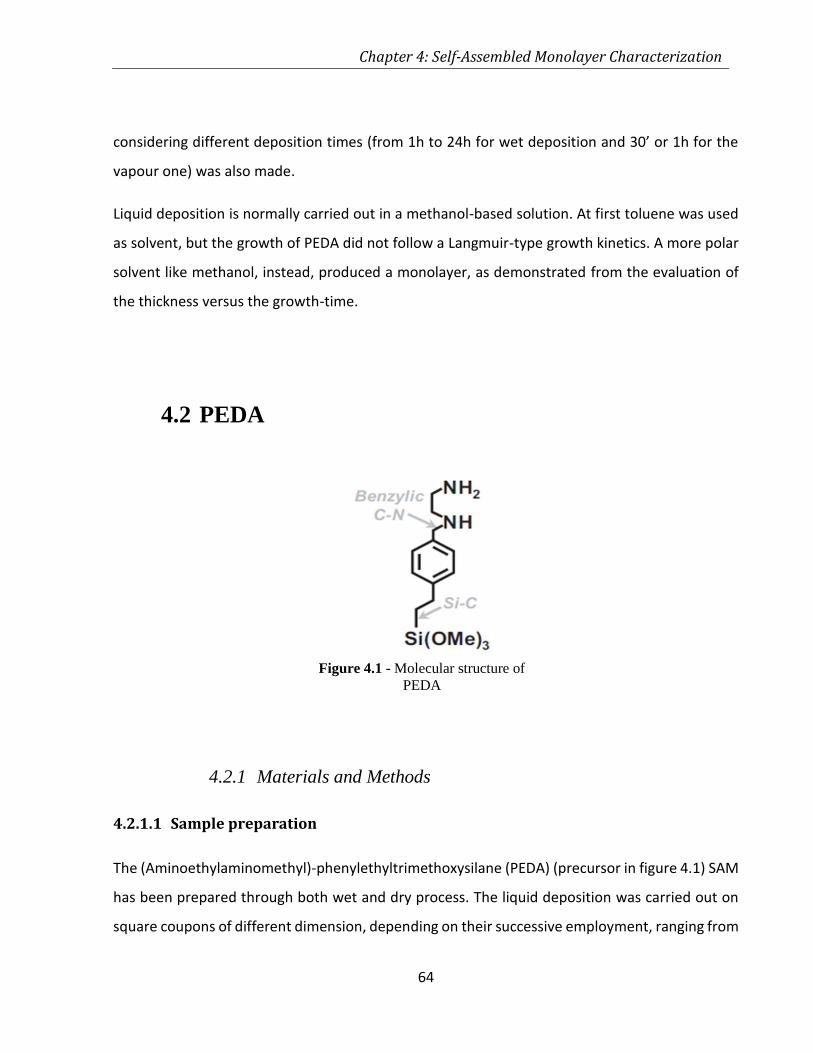
Chapter 4: Self-Assembled Monolayer Characterization
64
considering different deposition times (from 1h to 24h for wet deposition and 30’ or 1h for the
vapour one) was also made.
Liquid deposition is normally carried out in a methanol-based solution. At first toluene was used
as solvent, but the growth of PEDA did not follow a Langmuir-type growth kinetics. A more polar
solvent like methanol, instead, produced a monolayer, as demonstrated from the evaluation of
the thickness versus the growth-time.
4.2 PEDA
4.2.1 Materials and Methods
4.2.1.1 Sample preparation
The (Aminoethylaminomethyl)-phenylethyltrimethoxysilane (PEDA) (precursor in figure 4.1) SAM
has been prepared through both wet and dry process. The liquid deposition was carried out on
square coupons of different dimension, depending on their successive employment, ranging from
Figure 4.1 - Molecular structure of
PEDA
Chapter 4: Self-Assembled Monolayer Characterization
65
2x2 to 5.5x5.5 cm2. The coupon, previous to the actual deposition step, went through a cleaning
process, involving the use of the described Jealight Uv-Ozone cleaner. The coupons were then
freed from carbon residues and the surface was functionalized with –OH groups, necessary for
the SAM anchoring step. The PEDA precursor is then diluted, with a concentration of 5 mM, in a
methanol/water 95:5 v/v based solution, with acetic acid (1 mM). With such solution a perfect
deposition could be achieved, with a bright and shiny surface (it appears blurry and thick if
multilayer is deposited). Rinsing of the coupons is quite a complex step. It involved four different
rinsing passages in four different solvents of increasing polarity: starting from methanol, on which
the depositing solution is based, passing through acetone, ethanol and finally De-Ionized Water
(DIW), every time with a 2’ sonication. In such a way excessive molecules, eventually absorbed
on top of the monolayer and remains of the depositing solution, could effectively be removed. A
final drying with the N2 gun closed the liquid deposition process. Deposition times ranged from
1h to 24h depending on the specific application. It has to be underlined that the cleaning step
were normally done manually for patterned coupons, to avoid the collapse of the side of the
trenches or other features present on the sample.
The dry deposition followed the same cleaning process, with the same purposes, with the only
difference that full-wafer where processed. A full-wafer wet-deposition would be far more
complicated than the coupon one, because the rinsing/sonication process cannot be
accomplished effectively. In this sense, the dry deposition can be much more appealing to achieve
industrial scaling-up. The wafer, after cleaning, was positioned on a support, inside the
silanization oven, and brought to a temperature of 140 °C. The silane was deposited on a small
grid, above the wafer, working as a reservoir. The deposition was carried out at low pressure, 28
mbar, to avoid the co-deposition of contaminants on the wafer during the SAM formation.
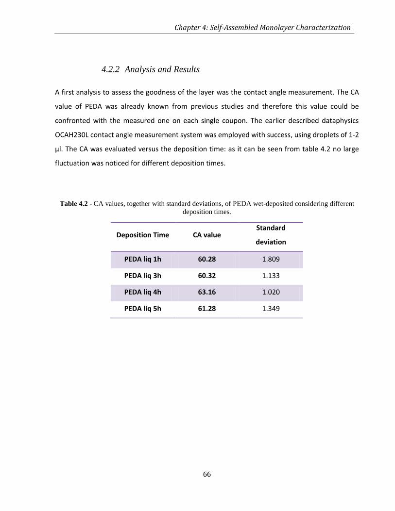
Chapter 4: Self-Assembled Monolayer Characterization
66
4.2.2 Analysis and Results
A first analysis to assess the goodness of the layer was the contact angle measurement. The CA
value of PEDA was already known from previous studies and therefore this value could be
confronted with the measured one on each single coupon. The earlier described dataphysics
OCAH230L contact angle measurement system was employed with success, using droplets of 1-2
μl. The CA was evaluated versus the deposition time: as it can be seen from table 4.2 no large
fluctuation was noticed for different deposition times.
Table 4.2 - CA values, together with standard deviations, of PEDA wet-deposited considering different
deposition times.
Deposition Time CA value Standard
deviation
PEDA liq 1h 60.28 1.809
PEDA liq 3h 60.32 1.133
PEDA liq 4h 63.16 1.020
PEDA liq 5h 61.28 1.349
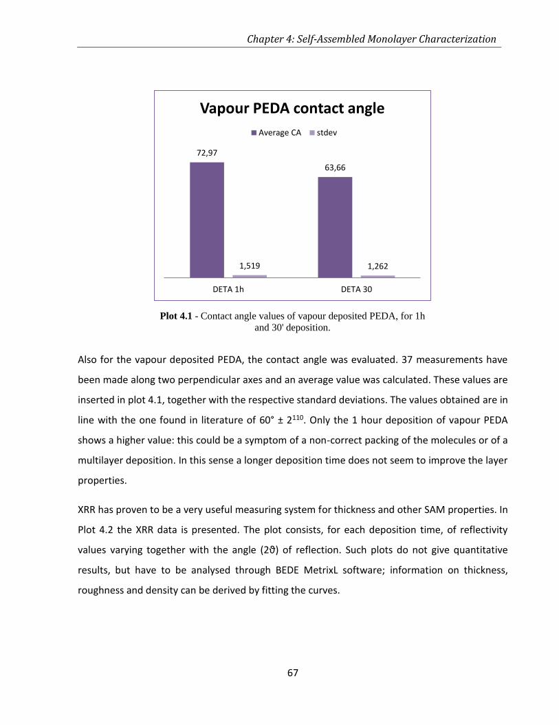
Chapter 4: Self-Assembled Monolayer Characterization
67
Also for the vapour deposited PEDA, the contact angle was evaluated. 37 measurements have
been made along two perpendicular axes and an average value was calculated. These values are
inserted in plot 4.1, together with the respective standard deviations. The values obtained are in
line with the one found in literature of 60° ± 2110. Only the 1 hour deposition of vapour PEDA
shows a higher value: this could be a symptom of a non-correct packing of the molecules or of a
multilayer deposition. In this sense a longer deposition time does not seem to improve the layer
properties.
XRR has proven to be a very useful measuring system for thickness and other SAM properties. In
Plot 4.2 the XRR data is presented. The plot consists, for each deposition time, of reflectivity
values varying together with the angle (2ϑ) of reflection. Such plots do not give quantitative
results, but have to be analysed through BEDE MetrixL software; information on thickness,
roughness and density can be derived by fitting the curves.
72,97
63,66
1,519 1,262
DETA 1h DETA 30
Vapour PEDA contact angle
Average CA stdev
Plot 4.1 - Contact angle values of vapour deposited PEDA, for 1h
and 30' deposition.
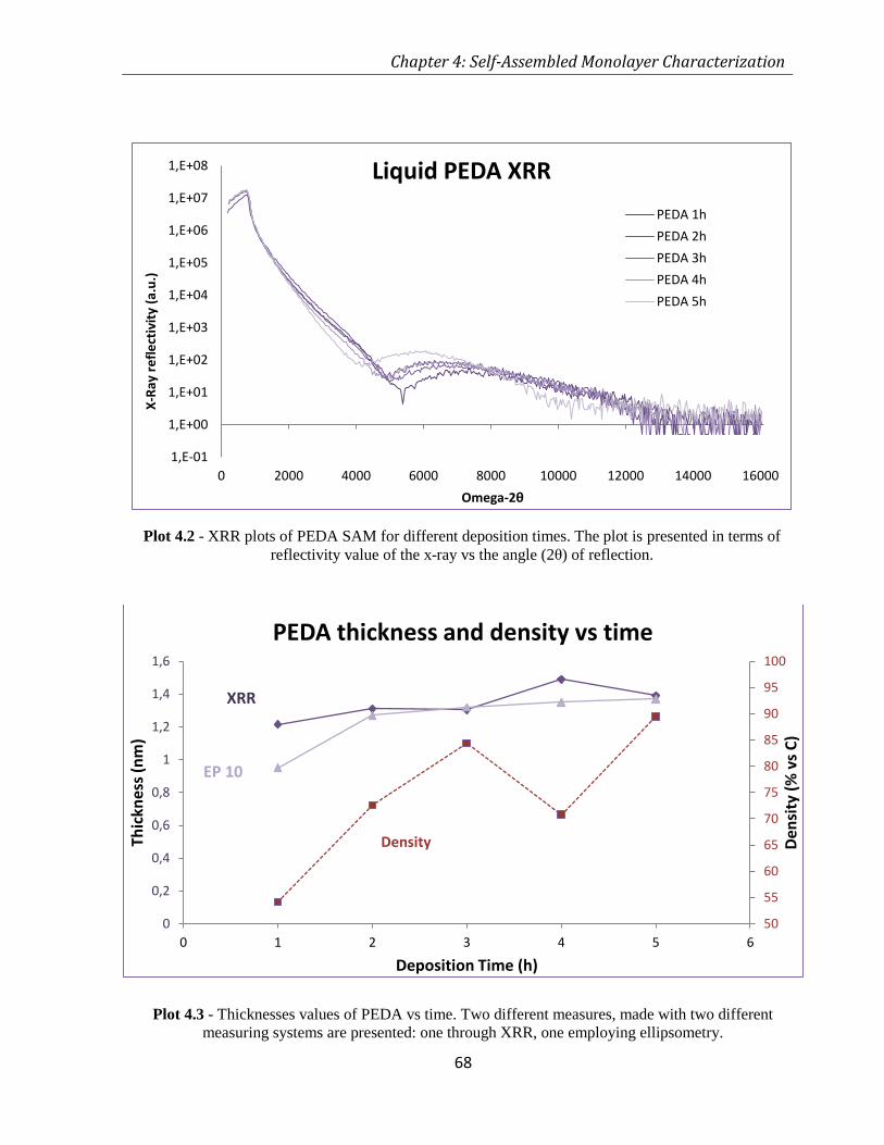
Chapter 4: Self-Assembled Monolayer Characterization
68
Plot 4.3 - Thicknesses values of PEDA vs time. Two different measures, made with two different
measuring systems are presented: one through XRR, one employing ellipsometry.
50
55
60
65
70
75
80
85
90
95
100
0
0,2
0,4
0,6
0,8
1
1,2
1,4
1,6
0 1 2 3 4 5 6
Den
sity
(%
vs
C)
Thic
knes
s (n
m)
Deposition Time (h)
PEDA thickness and density vs time
XRR
EP 10
Density
1,E-01
1,E+00
1,E+01
1,E+02
1,E+03
1,E+04
1,E+05
1,E+06
1,E+07
1,E+08
0 2000 4000 6000 8000 10000 12000 14000 16000
X-R
ay r
efl
ect
ivit
y (a
.u.)
Omega-2θ
Liquid PEDA XRR
PEDA 1h
PEDA 2h
PEDA 3h
PEDA 4h
PEDA 5h
Plot 4.2 - XRR plots of PEDA SAM for different deposition times. The plot is presented in terms of
reflectivity value of the x-ray vs the angle (2θ) of reflection.
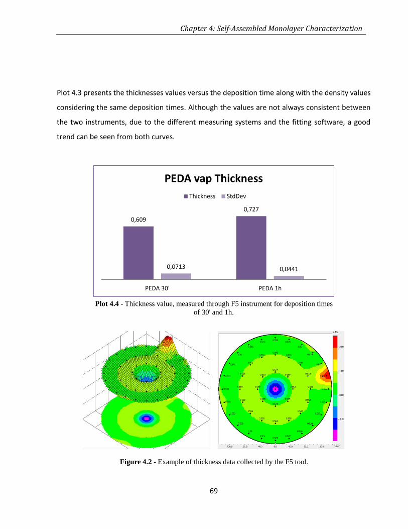
Chapter 4: Self-Assembled Monolayer Characterization
69
Plot 4.3 presents the thicknesses values versus the deposition time along with the density values
considering the same deposition times. Although the values are not always consistent between
the two instruments, due to the different measuring systems and the fitting software, a good
trend can be seen from both curves.
0,609
0,727
0,0713 0,0441
PEDA 30' PEDA 1h
PEDA vap Thickness
Thickness StdDev
Plot 4.4 - Thickness value, measured through F5 instrument for deposition times
of 30' and 1h.
Figure 4.2 - Example of thickness data collected by the F5 tool.
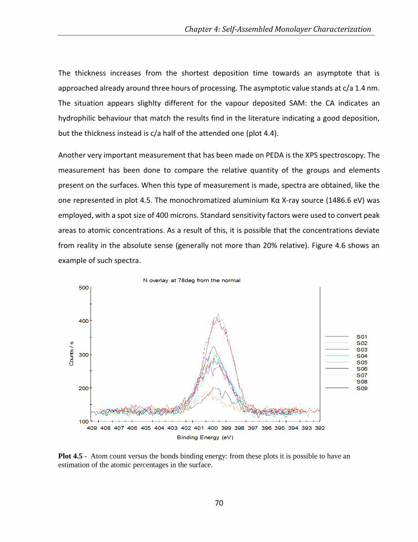
Chapter 4: Self-Assembled Monolayer Characterization
70
The thickness increases from the shortest deposition time towards an asymptote that is
approached already around three hours of processing. The asymptotic value stands at c/a 1.4 nm.
The situation appears slighlty different for the vapour deposited SAM: the CA indicates an
hydrophilic behaviour that match the results find in the literature indicating a good deposition,
but the thickness instead is c/a half of the attended one (plot 4.4).
Another very important measurement that has been made on PEDA is the XPS spectroscopy. The
measurement has been done to compare the relative quantity of the groups and elements
present on the surfaces. When this type of measurement is made, spectra are obtained, like the
one represented in plot 4.5. The monochromatized aluminium Kα X-ray source (1486.6 eV) was
employed, with a spot size of 400 microns. Standard sensitivity factors were used to convert peak
areas to atomic concentrations. As a result of this, it is possible that the concentrations deviate
from reality in the absolute sense (generally not more than 20% relative). Figure 4.6 shows an
example of such spectra.
Plot 4.5 - Atom count versus the bonds binding energy: from these plots it is possible to have an
estimation of the atomic percentages in the surface.
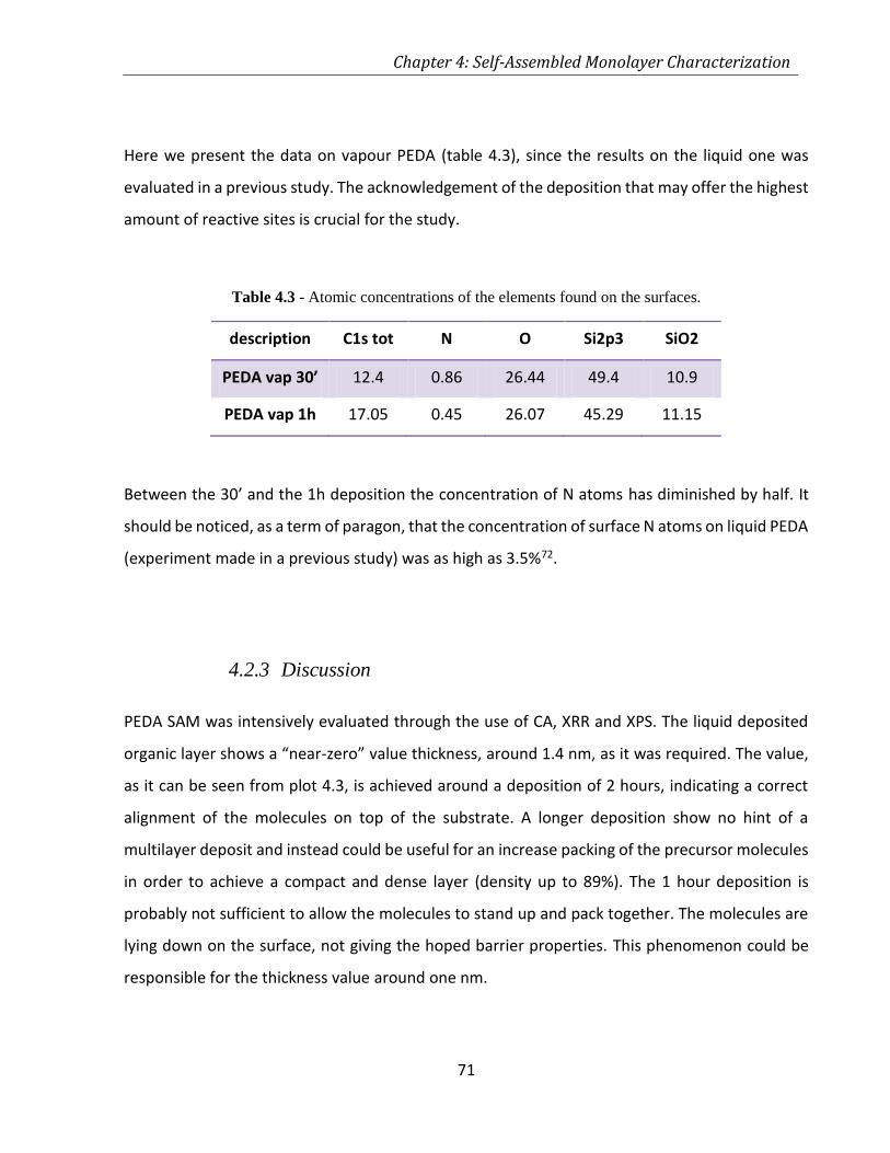
Chapter 4: Self-Assembled Monolayer Characterization
71
Here we present the data on vapour PEDA (table 4.3), since the results on the liquid one was
evaluated in a previous study. The acknowledgement of the deposition that may offer the highest
amount of reactive sites is crucial for the study.
Table 4.3 - Atomic concentrations of the elements found on the surfaces.
description C1s tot N O Si2p3 SiO2
PEDA vap 30’ 12.4 0.86 26.44 49.4 10.9
PEDA vap 1h 17.05 0.45 26.07 45.29 11.15
Between the 30’ and the 1h deposition the concentration of N atoms has diminished by half. It
should be noticed, as a term of paragon, that the concentration of surface N atoms on liquid PEDA
(experiment made in a previous study) was as high as 3.5%72.
4.2.3 Discussion
PEDA SAM was intensively evaluated through the use of CA, XRR and XPS. The liquid deposited
organic layer shows a “near-zero” value thickness, around 1.4 nm, as it was required. The value,
as it can be seen from plot 4.3, is achieved around a deposition of 2 hours, indicating a correct
alignment of the molecules on top of the substrate. A longer deposition show no hint of a
multilayer deposit and instead could be useful for an increase packing of the precursor molecules
in order to achieve a compact and dense layer (density up to 89%). The 1 hour deposition is
probably not sufficient to allow the molecules to stand up and pack together. The molecules are
lying down on the surface, not giving the hoped barrier properties. This phenomenon could be
responsible for the thickness value around one nm.
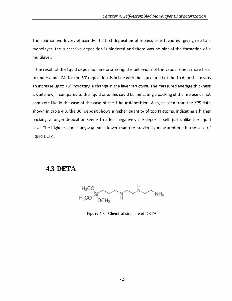
Chapter 4: Self-Assembled Monolayer Characterization
72
The solution work very efficiently: if a first deposition of molecules is favoured, giving rise to a
monolayer, the successive deposition is hindered and there was no hint of the formation of a
multilayer.
If the result of the liquid deposition are promising, the behaviour of the vapour one is more hard
to understand. CA, for the 30’ deposition, is in line with the liquid one but the 1h deposit showns
an increase up to 73° indicating a change in the layer structure. The measured average thickness
is quite low, if compared to the liquid one: this could be indicating a packing of the molecules not
complete like in the case of the case of the 1 hour deposition. Also, as seen from the XPS data
shown in table 4.3, the 30’ deposit shows a higher quantity of top N atoms, indicating a higher
packing: a longer deposition seems to affect negatively the deposit itself, just unlike the liquid
case. The higher value is anyway much lower than the previously measured one in the case of
liquid DETA.
4.3 DETA
Figure 4.3 - Chemical structure of DETA
Chapter 4: Self-Assembled Monolayer Characterization
73
4.3.1 Materials and Methods
4.3.1.1 Sample preparation
The (3-Trimethoxysilylpropyl)-diethylenetriamine (DETA) SAM, was deposited as an alternative
organic barrier layer for the first time during this work. The obvious choice was then to employ
the same technique successfully used for the PEDA liquid deposition, also for DETA. The result, as
we will see in the next pages, is very promising.
4.3.2 Analysis and Results
Contact angle measurements were made, as before, employing water as sessile liquid and are
presented in table 4.4.
Table 4.4 - CA values for liquid deposited DETA
Deposition Time CA value st.dev.
DETA liq 1h 62.22 3,20587
DETA liq 3h 58.5 2,519524
DETA liq 4h 57.74 2,97765
DETA liq 5h 56.42 0,231517
The CA appear to stabilize, after 5 hours of deposition, around a value of 56.4°. The value seems
legit, according to the values found in literature111.
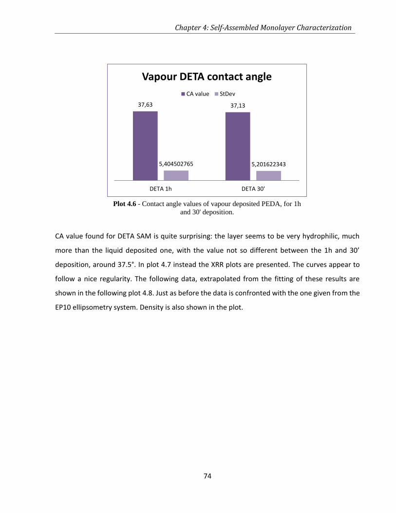
Chapter 4: Self-Assembled Monolayer Characterization
74
CA value found for DETA SAM is quite surprising: the layer seems to be very hydrophilic, much
more than the liquid deposited one, with the value not so different between the 1h and 30’
deposition, around 37.5°. In plot 4.7 instead the XRR plots are presented. The curves appear to
follow a nice regularity. The following data, extrapolated from the fitting of these results are
shown in the following plot 4.8. Just as before the data is confronted with the one given from the
EP10 ellipsometry system. Density is also shown in the plot.
37,63 37,13
5,404502765 5,201622343
DETA 1h DETA 30'
Vapour DETA contact angle
CA value StDev
Plot 4.6 - Contact angle values of vapour deposited PEDA, for 1h
and 30' deposition.
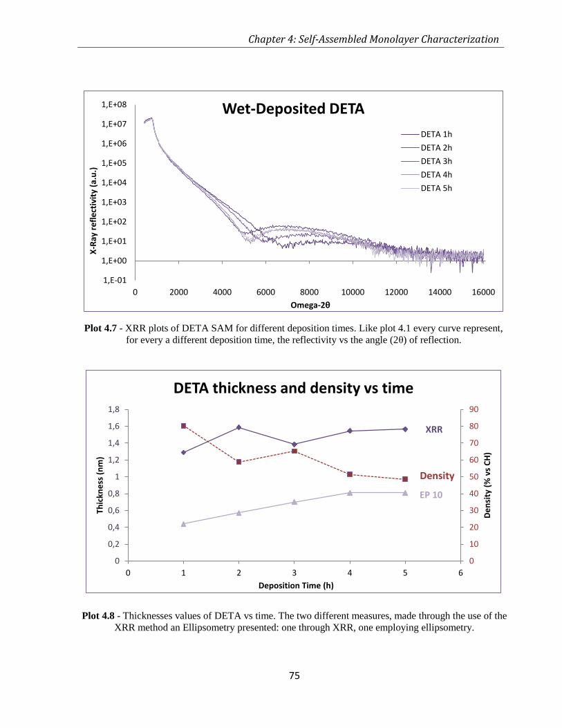
Chapter 4: Self-Assembled Monolayer Characterization
75
Plot 4.8 - Thicknesses values of DETA vs time. The two different measures, made through the use of the
XRR method an Ellipsometry presented: one through XRR, one employing ellipsometry.
0
10
20
30
40
50
60
70
80
90
0
0,2
0,4
0,6
0,8
1
1,2
1,4
1,6
1,8
0 1 2 3 4 5 6
De
nsi
ty (
% v
s C
H)
Thic
kne
ss (
nm
)
Deposition Time (h)
DETA thickness and density vs time
Density
1,E-01
1,E+00
1,E+01
1,E+02
1,E+03
1,E+04
1,E+05
1,E+06
1,E+07
1,E+08
0 2000 4000 6000 8000 10000 12000 14000 16000
X-R
ay r
efl
ect
ivit
y (a
.u.)
Omega-2θ
Wet-Deposited DETA
DETA 1h
DETA 2h
DETA 3h
DETA 4h
DETA 5h
Plot 4.7 - XRR plots of DETA SAM for different deposition times. Like plot 4.1 every curve represent,
for every a different deposition time, the reflectivity vs the angle (2θ) of reflection.
XRR
EP 10
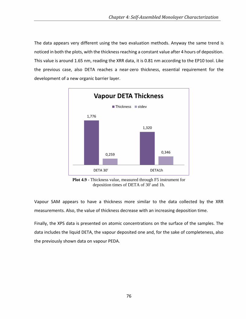
Chapter 4: Self-Assembled Monolayer Characterization
76
The data appears very different using the two evaluation methods. Anyway the same trend is
noticed in both the plots, with the thickness reaching a constant value after 4 hours of deposition.
This value is around 1.65 nm, reading the XRR data, it is 0.81 nm according to the EP10 tool. Like
the previous case, also DETA reaches a near-zero thickness, essential requirement for the
development of a new organic barrier layer.
Vapour SAM appears to have a thickness more similar to the data collected by the XRR
measurements. Also, the value of thickness decrease with an increasing deposition time.
Finally, the XPS data is presented on atomic concentrations on the surface of the samples. The
data includes the liquid DETA, the vapour deposited one and, for the sake of completeness, also
the previously shown data on vapour PEDA.
1,776
1,320
0,2590,346
DETA 30' DETA1h
Vapour DETA Thickness
Thickness stdev
Plot 4.9 - Thickness value, measured through F5 instrument for
deposition times of DETA of 30' and 1h.
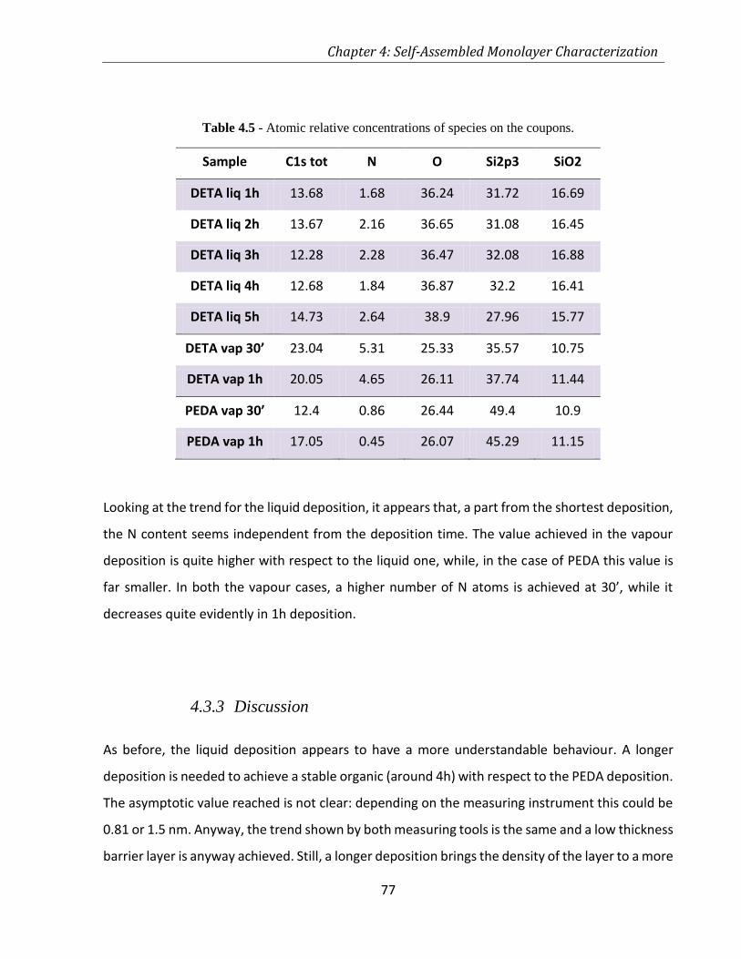
Chapter 4: Self-Assembled Monolayer Characterization
77
Table 4.5 - Atomic relative concentrations of species on the coupons.
Sample C1s tot N O Si2p3 SiO2
DETA liq 1h 13.68 1.68 36.24 31.72 16.69
DETA liq 2h 13.67 2.16 36.65 31.08 16.45
DETA liq 3h 12.28 2.28 36.47 32.08 16.88
DETA liq 4h 12.68 1.84 36.87 32.2 16.41
DETA liq 5h 14.73 2.64 38.9 27.96 15.77
DETA vap 30’ 23.04 5.31 25.33 35.57 10.75
DETA vap 1h 20.05 4.65 26.11 37.74 11.44
PEDA vap 30’ 12.4 0.86 26.44 49.4 10.9
PEDA vap 1h 17.05 0.45 26.07 45.29 11.15
Looking at the trend for the liquid deposition, it appears that, a part from the shortest deposition,
the N content seems independent from the deposition time. The value achieved in the vapour
deposition is quite higher with respect to the liquid one, while, in the case of PEDA this value is
far smaller. In both the vapour cases, a higher number of N atoms is achieved at 30’, while it
decreases quite evidently in 1h deposition.
4.3.3 Discussion
As before, the liquid deposition appears to have a more understandable behaviour. A longer
deposition is needed to achieve a stable organic (around 4h) with respect to the PEDA deposition.
The asymptotic value reached is not clear: depending on the measuring instrument this could be
0.81 or 1.5 nm. Anyway, the trend shown by both measuring tools is the same and a low thickness
barrier layer is anyway achieved. Still, a longer deposition brings the density of the layer to a more
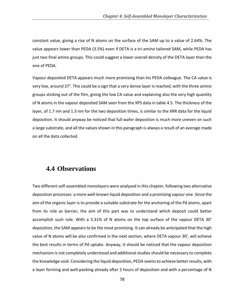
Chapter 4: Self-Assembled Monolayer Characterization
78
constant value, giving a rise of N atoms on the surface of the SAM up to a value of 2.64%. The
value appears lower than PEDA (3.5%) even if DETA is a tri-amino tailored SAM, while PEDA has
just two final amino groups. This could suggest a lower overall density of the DETA layer than the
one of PEDA.
Vapour deposited DETA appears much more promising than his PEDA colleague. The CA value is
very low, around 37°. This could be a sign that a very dense layer is reached, with the three amino
groups sticking out of the film, giving the low CA value and explaining also the very high quantity
of N atoms in the vapour deposited SAM seen from the XPS data in table 4.5. The thickness of the
layer, of 1.7 nm and 1.3 nm for the two deposition times, is similar to the XRR data for the liquid
deposition. It should anyway be noticed that full wafer deposition is much more uneven on such
a large substrate, and all the values shown in this paragraph is always a result of an average made
on all the data collected.
4.4 Observations
Two different self-assembled monolayers were analysed in this chapter, following two alternative
deposition processes: a more well-known liquid deposition and a promising vapour one. Since the
aim of the organic layer is to provide a suitable substrate for the anchoring of the Pd atoms, apart
from its role as barrier, the aim of this part was to understand which deposit could better
accomplish such role. With a 5.31% of N atoms on the top surface of the vapour DETA 30’
deposition, the SAM appears to be the most promising. It can already be anticipated that the high
value of N atoms will be also confirmed in the next section, where DETA vapour 30’, will achieve
the best results in terms of Pd uptake. Anyway, it should be noticed that the vapour deposition
mechanism is not completely understood and additional studies should be necessary to complete
the knowledge void. Considering the liquid deposition, PEDA seems to achieve better results, with
a layer forming and well-packing already after 2 hours of deposition and with a percentage of N
Chapter 4: Self-Assembled Monolayer Characterization
79
surface atoms that goes up to 3.5% for a 5 hours deposition. The value is quite surprising
considering the lower amount of amino- groups possessed by the PEDA precursor with respect to
the DETA SAM precursor, which contains three of them, reaching a highest value of 2.64% for the
same deposition time and processing. The DETA film, deposited from liquid solutions, does not
show the hoped densities and catalysing abilities, even if it can be still considered a good barrier
layer. A more complete comparison will be made when coupled with the metal layer. Overall,
liquid PEDA appears more promising, reaching higher density values and thickness consistency
over different deposition rimes as evaluated through XRR. On the contrary, obtaining the same
layer properties with a vapour deposition appears much more complex.
Chapter 5: Electroless Deposition of NiB on SAM
80
Chapter 5: Electroless Deposition
of NiB on SAM
The next step on the road to the formation of a complete interconnection system is the deposition
of the metal over the barrier layer. The chapter will then be focusing on the metal deposit
characteristics and properties by presenting the results achieved through the experiments
realized in this work.
5.1 Introduction
The chapter can be broadly divided in three main parts. The first part will not be focusing on the
metal per se but more on the catalyser. The palladium deposit on the SAM will be under focus to
evaluate the situation where the highest amount of catalyser deposition is achieved. This was
made through the use of XPS spectroscopy. The second part will be focusing on the NiB layer:
analysing thickness and measuring resistivity with different deposition times, the characteristics
of the deposit will be under consideration. Finally the best deposit, combined with the best
organic barrier layer will be used to evaluate the line resistivity on patterned silicon.
Main goal of the deposition is to achieve a metal that may work as a good barrier layer metal,
actively contributing to the overall conductivity of the interconnection, or autonomously compete
with the other metal currently employed in the interconnection industry. Along with low
resistivity, essential for both tasks, the metal has to respect some other process conditions that
will have to be evaluated. A part from the requirement of blocking the diffusion between silicon
and NiB, also good conformity is appreciated while high thicknesses are reached, essential for a
Chapter 5: Electroless Deposition of NiB on SAM
81
good CMP process. The adhesion is also an important feature of the film since the next processing
steps in the IC industry have high requirements in terms of mechanical solicitation. All these
characteristics where evaluated and are exposed in the following paragraphs.
5.2 Palladium deposition
The study of Pd deposition is made through the use of a PdCl2-based commercial solution
provided by LAM® Research while the measuring system (Atomika TXRF8300W) was described in
3.6.
5.2.1 Materials and Methods
5.2.1.1 Sample preparation
3x3 cm2 coupons of silicon have been prepared for the experiments. Following the conventional
cleaning steps both SAMs, PEDA and DETA, where deposited on the coupons with the liquid
processing time ranging from 1 hour to 5 with steps of 1 hour. The vapour deposition instead
followed the conventional 30’ and 1 hour deposition. The Pd deposition was carried in 4
successive steps:
Rinse in DIW, 30’’;
Immersion in the PdCl2 solution, 5’;
Rinse in diluted Additive M, 2’;
Final rinsing in water 30’’.
The rinse in Additive M (provided by LAM® Research and whose composition is unknown), diluted
in water with the same concentration as the one present in the metal depositing solution, is
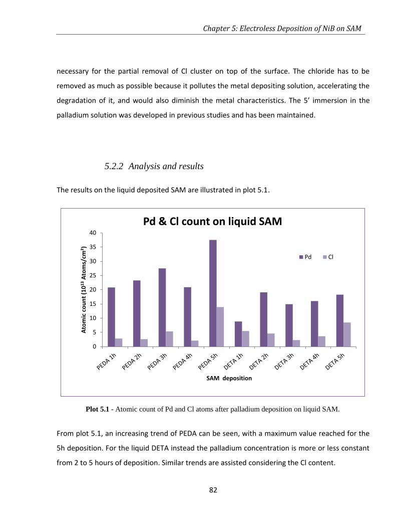
Chapter 5: Electroless Deposition of NiB on SAM
82
necessary for the partial removal of Cl cluster on top of the surface. The chloride has to be
removed as much as possible because it pollutes the metal depositing solution, accelerating the
degradation of it, and would also diminish the metal characteristics. The 5’ immersion in the
palladium solution was developed in previous studies and has been maintained.
5.2.2 Analysis and results
The results on the liquid deposited SAM are illustrated in plot 5.1.
From plot 5.1, an increasing trend of PEDA can be seen, with a maximum value reached for the
5h deposition. For the liquid DETA instead the palladium concentration is more or less constant
from 2 to 5 hours of deposition. Similar trends are assisted considering the Cl content.
0
5
10
15
20
25
30
35
40
Ato
mic
co
un
t (1
01
3A
tom
s/cm
²)
SAM deposition
Pd & Cl count on liquid SAM
Pd Cl
Plot 5.1 - Atomic count of Pd and Cl atoms after palladium deposition on liquid SAM.
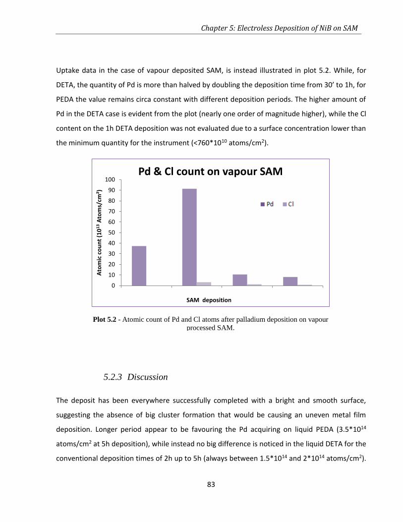
Chapter 5: Electroless Deposition of NiB on SAM
83
Uptake data in the case of vapour deposited SAM, is instead illustrated in plot 5.2. While, for
DETA, the quantity of Pd is more than halved by doubling the deposition time from 30’ to 1h, for
PEDA the value remains circa constant with different deposition periods. The higher amount of
Pd in the DETA case is evident from the plot (nearly one order of magnitude higher), while the Cl
content on the 1h DETA deposition was not evaluated due to a surface concentration lower than
the minimum quantity for the instrument (<760*1010 atoms/cm2).
5.2.3 Discussion
The deposit has been everywhere successfully completed with a bright and smooth surface,
suggesting the absence of big cluster formation that would be causing an uneven metal film
deposition. Longer period appear to be favouring the Pd acquiring on liquid PEDA (3.5*1014
atoms/cm2 at 5h deposition), while instead no big difference is noticed in the liquid DETA for the
conventional deposition times of 2h up to 5h (always between 1.5*1014 and 2*1014 atoms/cm2).
0
10
20
30
40
50
60
70
80
90
100
Ato
mic
co
un
t (1
01
3A
tom
s/cm
²)
SAM deposition
Pd & Cl count on vapour SAM
PD Cl
Plot 5.2 - Atomic count of Pd and Cl atoms after palladium deposition on vapour
processed SAM.
Chapter 5: Electroless Deposition of NiB on SAM
84
It should be noticed that the Pd uptake in liquid DETA follows the same trend as the quantity of
N atoms found on the top of the same organic layer, as it is shown in table 4.5. The higher count
on the liquid PEDA layer is probably due to a higher packing of the organic molecules that permit
the binding of a higher number of the Pd atoms. Comparing, as before, the result of the Pd uptake
with the quantity of N groups of the SAM, previous studies have shown how the percentage of
amino- groups on top of PEDA is higher than DETA (3.5 vs 2.64 at 5h liquid deposition). This
explains the better results of PEDA with respect to DETA in the palladium uptake.
If in the liquid case a better job is achieved by PEDA, even if the difference is not so evident
between the two SAMs, in the vapour deposition process far better results are measured for DETA
than for PEDA. Also, as expected, the 30’ deposition seems to be more useful than the 1h one.
5.3 Electroless Deposition of NiB
The work described in the previous chapter, involving the two organic self-assembled
monolayers, PEDA and DETA, that where employed in this work and with the Pd uptake analysis,
gave good results for both the films. Therefore, both SAMs where employed in the successive
metal deposition steps. This chapter will be presenting the most important results that were
achieved in this central part of the project, that’s to say the electroless deposition of NiB.
5.3.1 Materials and Method
5.3.1.1 Sample preparation
As already said in the previous chapters, during this project two different ELD solution where
used. The exact composition of the solutions is an industrial secret belonging to LAM® Research,
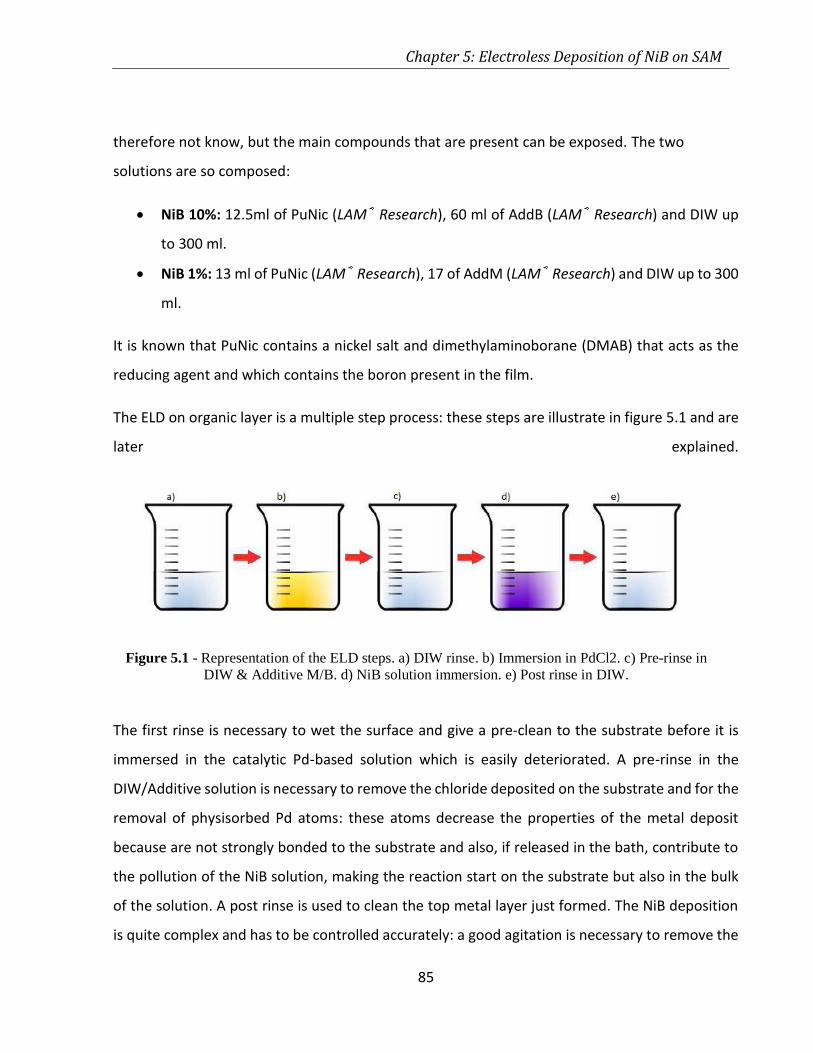
Chapter 5: Electroless Deposition of NiB on SAM
85
therefore not know, but the main compounds that are present can be exposed. The two
solutions are so composed:
NiB 10%: 12.5ml of PuNic (LAM® Research), 60 ml of AddB (LAM® Research) and DIW up
to 300 ml.
NiB 1%: 13 ml of PuNic (LAM® Research), 17 of AddM (LAM® Research) and DIW up to 300
ml.
It is known that PuNic contains a nickel salt and dimethylaminoborane (DMAB) that acts as the
reducing agent and which contains the boron present in the film.
The ELD on organic layer is a multiple step process: these steps are illustrate in figure 5.1 and are
later explained.
The first rinse is necessary to wet the surface and give a pre-clean to the substrate before it is
immersed in the catalytic Pd-based solution which is easily deteriorated. A pre-rinse in the
DIW/Additive solution is necessary to remove the chloride deposited on the substrate and for the
removal of physisorbed Pd atoms: these atoms decrease the properties of the metal deposit
because are not strongly bonded to the substrate and also, if released in the bath, contribute to
the pollution of the NiB solution, making the reaction start on the substrate but also in the bulk
of the solution. A post rinse is used to clean the top metal layer just formed. The NiB deposition
is quite complex and has to be controlled accurately: a good agitation is necessary to remove the
Figure 5.1 - Representation of the ELD steps. a) DIW rinse. b) Immersion in PdCl2. c) Pre-rinse in
DIW & Additive M/B. d) NiB solution immersion. e) Post rinse in DIW.
Chapter 5: Electroless Deposition of NiB on SAM
86
H2 bubbles that are formed during the deposition process. These bubbles decrease the properties
of the growing layer due to the formation of voids in the film and may also be a cause of hydrogen
cracking in later stages.
It should be noticed that in the previous process the pre-rinse step was carried out in pure DIW.
During the development of this project it was noticed that a pre-rinse in a solution DIW-based
with Add M or B (depending on which NiB solution was used) with the same concentration as the
following depositing solution, gave better results in terms of fast growth and resistivity of the
metal layer.
The deposition steps, from the first pre-clean to the post-rinse was carried out inside the glovebox
in picture 3.12.
5.3.1.2 Analysis techniques
The growth of the metal was analysed in order to have a better understanding of the deposition
process, using mainly x-ray reflectivity as characterization method. The resistance was evaluated
for different thicknesses so that the condition to have the best conductivity could be achieved.
The four point probe, in the line arrangement, has been used for this purpose. Together with
these important results, other properties have been evaluated and will be presented in the
following pages.
5.3.2 Thin Film Resistivity
5.3.2.1 Process description
In the first part of this project the goal was the measurement of the metal thin-film resistivity. A
high number of 3x3 cm2 coupons where produced in order to cover all possible range of
Chapter 5: Electroless Deposition of NiB on SAM
87
deposition options so that a complete overview of the process could be reached. The results on
the liquid SAMs are exposed first, just after the one on the vapour deposited one. The deposition
options, presented during the deposition of the barrier and metal stack, regarded:
the significant deposition times of the SAM;
whether or not anneal the samples post SAM deposition;
which NiB ELD time was most significant;
the understanding of the effect of the metal annealing.
Since no decision could be made a priori, to have a full cover of all possibility all deposition
specifics where covered. The SAM layer was processed with two significant deposition times: 2h
and 5h, so that the range of successful organic layer depositions is covered. Copies of the same
blanket where produce so that half could go through the SAM annealing step while the other half
did not. Also two deposition times where used in the metal deposition step: 3’ and 6’ where used
for the 10% NiB chemistry while for the 1%, 6’ and 12’ where considered more significant. These
is because of the highest amount of additive in the 10% chemistry is expected to cause a boost in
the deposition rate. Resistance and thickness where first evaluated on these coupons, while later
they underwent an annealing steps. Resistance was so evaluated also post-anneal while a nominal
decrease of thickness was assumed due to a recrystallization event during the annealing phase.
SAM Anneal was carried out at 120 °C, for 15 minutes under a N2 flux. The temperature was
chosen after previous studies have demonstrated that it did not affect negatively the organic
layer. The metal anneal was made in a heatpulse anneal oven at the temperature of 350 °C for 15
minutes in a forming gas (FOG) atmosphere. At this temperature the SAM layer should be able to
prevent interdiffusion while crystal reorganization is happening. A reduction of the 20% was taken
in account with the annealing process, due to crystalline rearrangement.
Chapter 5: Electroless Deposition of NiB on SAM
88
5.3.2.2 Results presentation
In the following graphs, all the data collected on the resistivity of NiB films, for different
thicknesses is illustrated. The value obtained for every coupon is the result of the average made
on 5 measurements made on each single specimen.
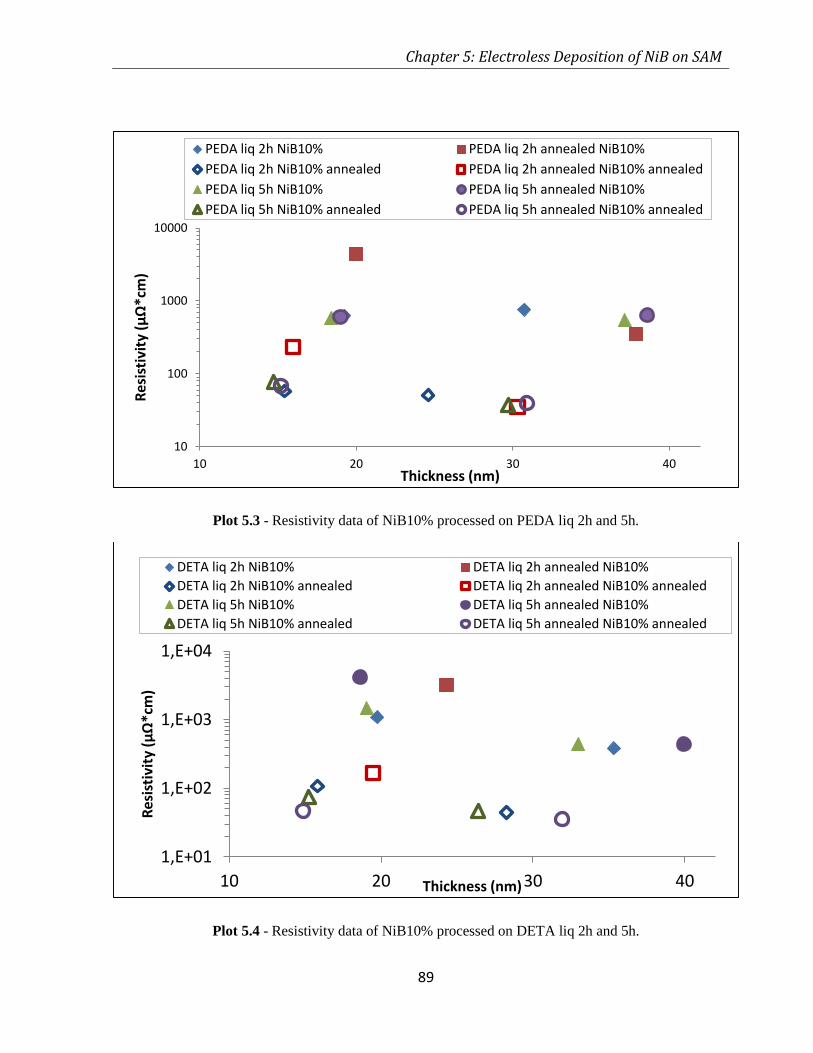
Chapter 5: Electroless Deposition of NiB on SAM
89
Plot 5.3 - Resistivity data of NiB10% processed on PEDA liq 2h and 5h.
Plot 5.4 - Resistivity data of NiB10% processed on DETA liq 2h and 5h.
10
100
1000
10000
10 20 30 40
Res
isti
vity
(µ
Ω*c
m)
Thickness (nm)
PEDA liq 2h NiB10% PEDA liq 2h annealed NiB10%
PEDA liq 2h NiB10% annealed PEDA liq 2h annealed NiB10% annealed
PEDA liq 5h NiB10% PEDA liq 5h annealed NiB10%
PEDA liq 5h NiB10% annealed PEDA liq 5h annealed NiB10% annealed
1,E+01
1,E+02
1,E+03
1,E+04
10 20 30 40
Res
isti
vity
(µ
Ω*c
m)
Thickness (nm)
DETA liq 2h NiB10% DETA liq 2h annealed NiB10%
DETA liq 2h NiB10% annealed DETA liq 2h annealed NiB10% annealed
DETA liq 5h NiB10% DETA liq 5h annealed NiB10%
DETA liq 5h NiB10% annealed DETA liq 5h annealed NiB10% annealed
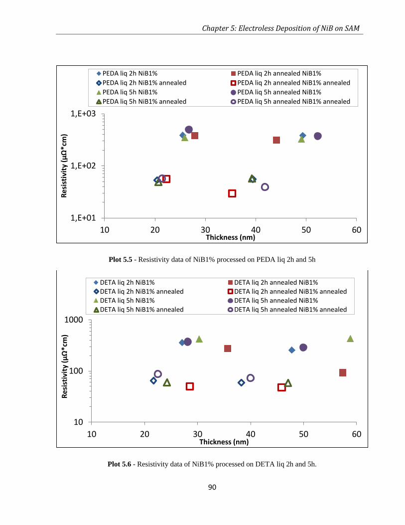
Chapter 5: Electroless Deposition of NiB on SAM
90
Plot 5.5 - Resistivity data of NiB1% processed on PEDA liq 2h and 5h
Plot 5.6 - Resistivity data of NiB1% processed on DETA liq 2h and 5h.
1,E+01
1,E+02
1,E+03
10 20 30 40 50 60
Res
isti
vity
(µ
Ω*c
m)
Thickness (nm)
PEDA liq 2h NiB1% PEDA liq 2h annealed NiB1%
PEDA liq 2h NiB1% annealed PEDA liq 2h annealed NiB1% annealed
PEDA liq 5h NiB1% PEDA liq 5h annealed NiB1%
PEDA liq 5h NiB1% annealed PEDA liq 5h annealed NiB1% annealed
10
100
1000
10 20 30 40 50 60
Res
isti
vity
(µ
Ω*c
m)
Thickness (nm)
DETA liq 2h NiB1% DETA liq 2h annealed NiB1%DETA liq 2h NiB1% annealed DETA liq 2h annealed NiB1% annealedDETA liq 5h NiB1% DETA liq 5h annealed NiB1%DETA liq 5h NiB1% annealed DETA liq 5h annealed NiB1% annealed
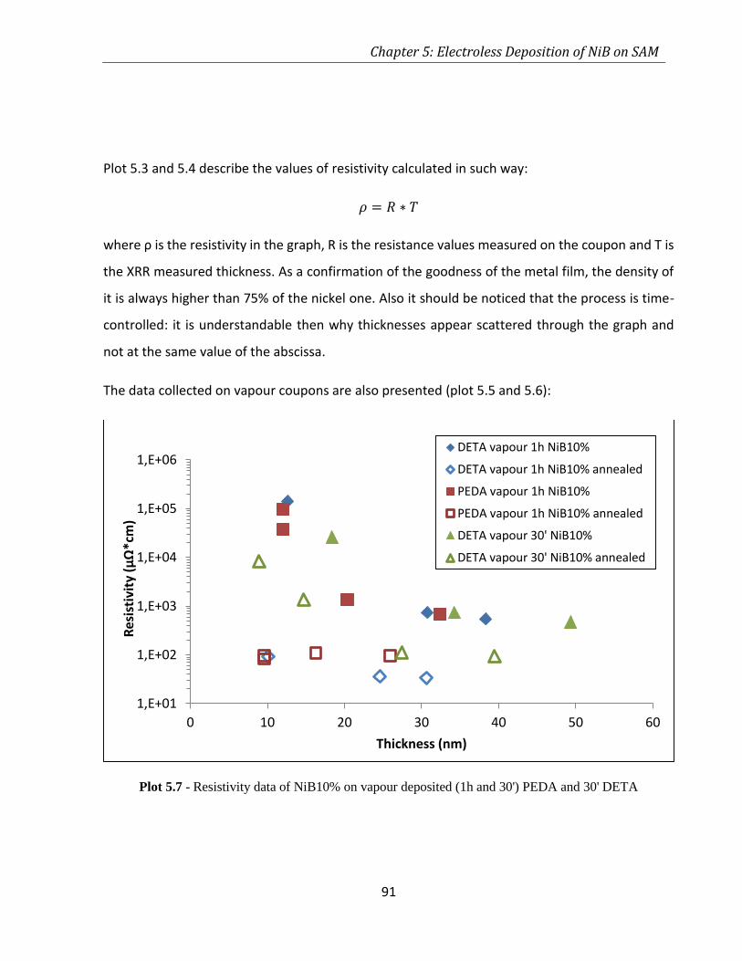
Chapter 5: Electroless Deposition of NiB on SAM
91
Plot 5.3 and 5.4 describe the values of resistivity calculated in such way:
𝜌 = 𝑅 ∗ 𝑇
where ρ is the resistivity in the graph, R is the resistance values measured on the coupon and T is
the XRR measured thickness. As a confirmation of the goodness of the metal film, the density of
it is always higher than 75% of the nickel one. Also it should be noticed that the process is time-
controlled: it is understandable then why thicknesses appear scattered through the graph and
not at the same value of the abscissa.
The data collected on vapour coupons are also presented (plot 5.5 and 5.6):
Plot 5.7 - Resistivity data of NiB10% on vapour deposited (1h and 30') PEDA and 30' DETA
1,E+01
1,E+02
1,E+03
1,E+04
1,E+05
1,E+06
0 10 20 30 40 50 60
Res
isti
vity
(µ
Ω*
cm)
Thickness (nm)
DETA vapour 1h NiB10%
DETA vapour 1h NiB10% annealed
PEDA vapour 1h NiB10%
PEDA vapour 1h NiB10% annealed
DETA vapour 30' NiB10%
DETA vapour 30' NiB10% annealed
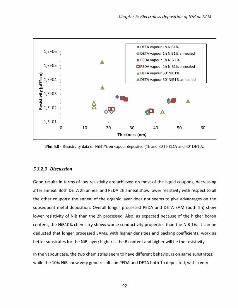
Chapter 5: Electroless Deposition of NiB on SAM
92
Plot 5.8 - Resistivity data of NiB1% on vapour deposited (1h and 30') PEDA and 30' DETA.
5.3.2.3 Discussion
Good results in terms of low resistivity are achieved on most of the liquid coupons, decreasing
after anneal. Both DETA 2h anneal and PEDA 2h anneal show lower resistivity with respect to all
the other coupons: the anneal of the organic layer does not seems to give advantages on the
subsequent metal deposition. Overall longer processed PEDA and DETA SAM (both 5h) show
lower resistivity of NiB than the 2h processed. Also, as expected because of the higher boron
content, the NiB10% chemistry shows worse conductivity properties than the NiB 1%. It can be
deducted that longer processed SAMs, with higher densities and packing coefficients, work as
better substrates for the NiB layer; higher is the B content and higher will be the resistivity.
In the vapour case, the two chemistries seem to have different behaviours on same substrates:
while the 10% NiB show very good results on PEDA and DETA both 1h deposited, with a very
1,E+01
1,E+02
1,E+03
1,E+04
1,E+05
1,E+06
0 10 20 30 40 50 60
Res
isti
vity
(µ
Ω*c
m)
Thickness (nm)
DETA vapour 1h NiB1%
DETA vapour 1h NiB1% annealed
PEDA vapour 1h NiB 1%
PEDA vapour 1h NiB1% annealed
DETA vapour 30' NiB1%
DETA vapour 30' NiB1% annealed
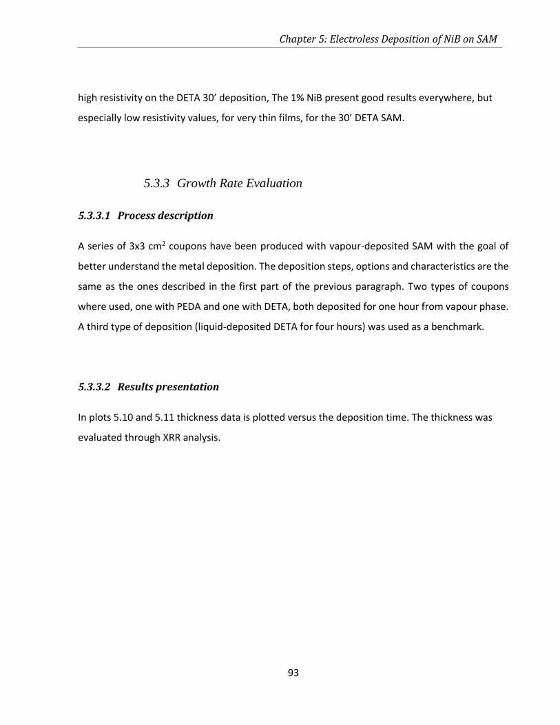
Chapter 5: Electroless Deposition of NiB on SAM
93
high resistivity on the DETA 30’ deposition, The 1% NiB present good results everywhere, but
especially low resistivity values, for very thin films, for the 30’ DETA SAM.
5.3.3 Growth Rate Evaluation
5.3.3.1 Process description
A series of 3x3 cm2 coupons have been produced with vapour-deposited SAM with the goal of
better understand the metal deposition. The deposition steps, options and characteristics are the
same as the ones described in the first part of the previous paragraph. Two types of coupons
where used, one with PEDA and one with DETA, both deposited for one hour from vapour phase.
A third type of deposition (liquid-deposited DETA for four hours) was used as a benchmark.
5.3.3.2 Results presentation
In plots 5.10 and 5.11 thickness data is plotted versus the deposition time. The thickness was
evaluated through XRR analysis.
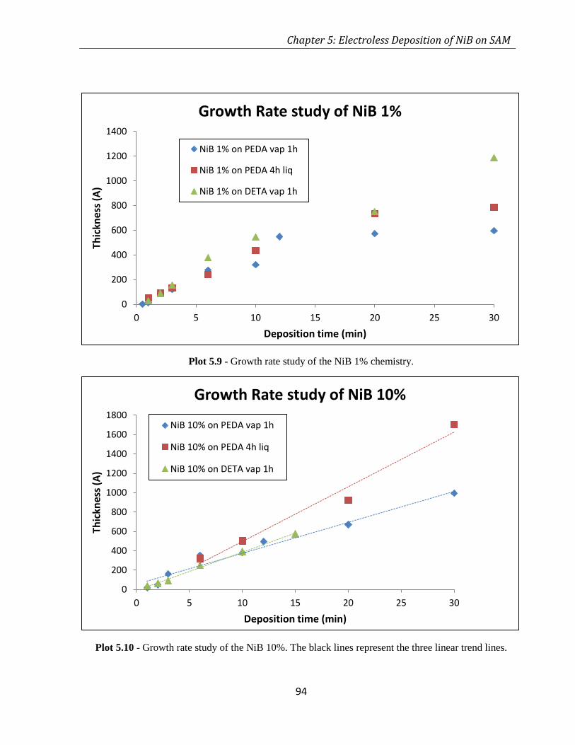
Chapter 5: Electroless Deposition of NiB on SAM
94
Plot 5.9 - Growth rate study of the NiB 1% chemistry.
Plot 5.10 - Growth rate study of the NiB 10%. The black lines represent the three linear trend lines.
0
200
400
600
800
1000
1200
1400
0 5 10 15 20 25 30
Thic
knes
s (A
)
Deposition time (min)
Growth Rate study of NiB 1%
NiB 1% on PEDA vap 1h
NiB 1% on PEDA 4h liq
NiB 1% on DETA vap 1h
0
200
400
600
800
1000
1200
1400
1600
1800
0 5 10 15 20 25 30
Thic
knes
s (A
)
Deposition time (min)
Growth Rate study of NiB 10%
NiB 10% on PEDA vap 1h
NiB 10% on PEDA 4h liq
NiB 10% on DETA vap 1h
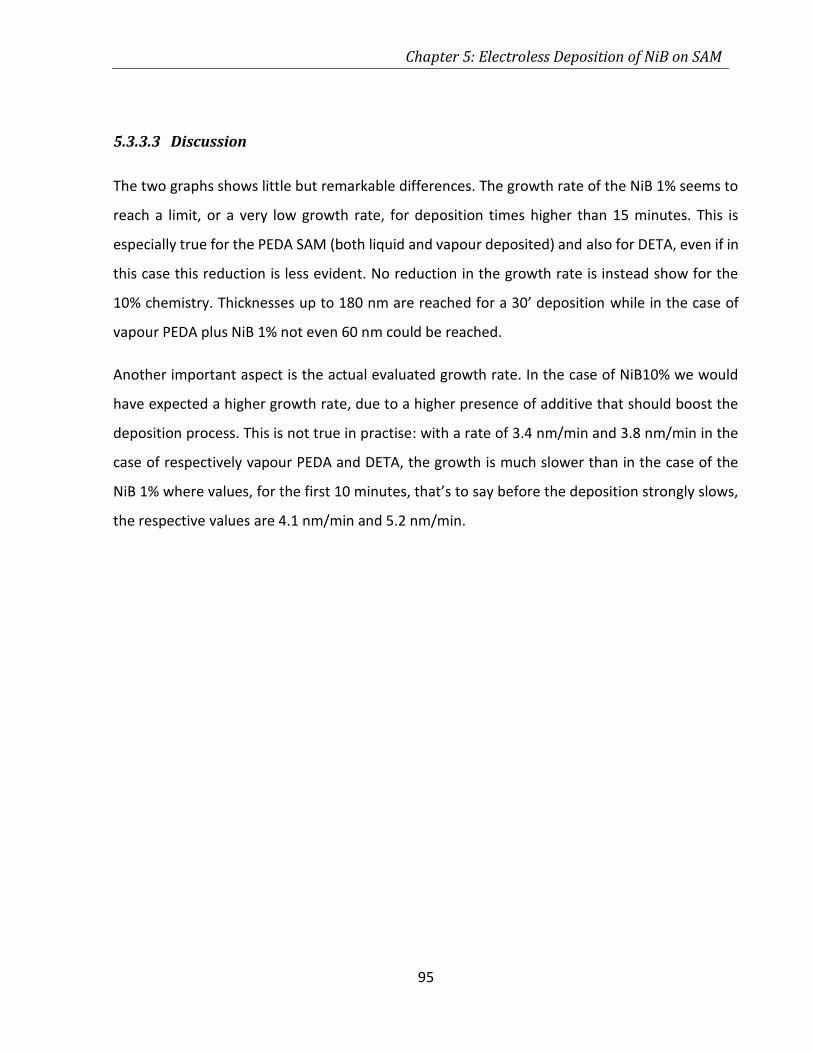
Chapter 5: Electroless Deposition of NiB on SAM
95
5.3.3.3 Discussion
The two graphs shows little but remarkable differences. The growth rate of the NiB 1% seems to
reach a limit, or a very low growth rate, for deposition times higher than 15 minutes. This is
especially true for the PEDA SAM (both liquid and vapour deposited) and also for DETA, even if in
this case this reduction is less evident. No reduction in the growth rate is instead show for the
10% chemistry. Thicknesses up to 180 nm are reached for a 30’ deposition while in the case of
vapour PEDA plus NiB 1% not even 60 nm could be reached.
Another important aspect is the actual evaluated growth rate. In the case of NiB10% we would
have expected a higher growth rate, due to a higher presence of additive that should boost the
deposition process. This is not true in practise: with a rate of 3.4 nm/min and 3.8 nm/min in the
case of respectively vapour PEDA and DETA, the growth is much slower than in the case of the
NiB 1% where values, for the first 10 minutes, that’s to say before the deposition strongly slows,
the respective values are 4.1 nm/min and 5.2 nm/min.
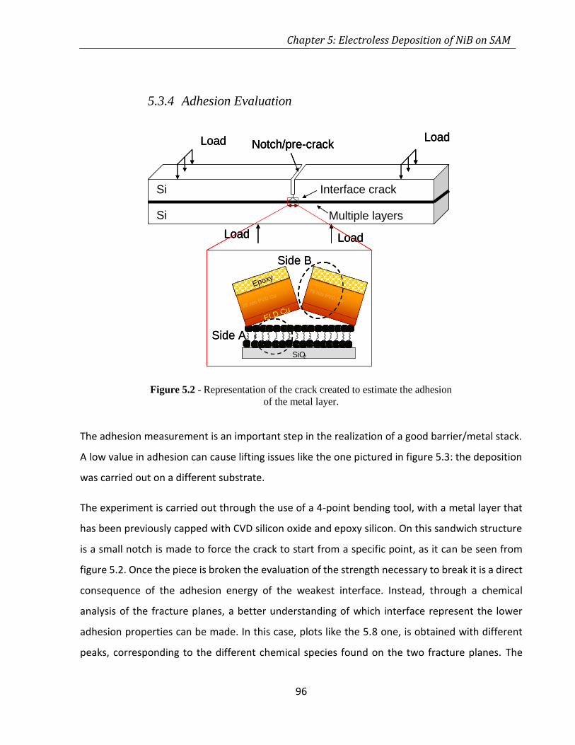
Chapter 5: Electroless Deposition of NiB on SAM
96
5.3.4 Adhesion Evaluation
The adhesion measurement is an important step in the realization of a good barrier/metal stack.
A low value in adhesion can cause lifting issues like the one pictured in figure 5.3: the deposition
was carried out on a different substrate.
The experiment is carried out through the use of a 4-point bending tool, with a metal layer that
has been previously capped with CVD silicon oxide and epoxy silicon. On this sandwich structure
is a small notch is made to force the crack to start from a specific point, as it can be seen from
figure 5.2. Once the piece is broken the evaluation of the strength necessary to break it is a direct
consequence of the adhesion energy of the weakest interface. Instead, through a chemical
analysis of the fracture planes, a better understanding of which interface represent the lower
adhesion properties can be made. In this case, plots like the 5.8 one, is obtained with different
peaks, corresponding to the different chemical species found on the two fracture planes. The
Notch/pre-crack
Interface crack
Multiple layers
Si
Si
LoadLoad
Load Load
SiO2
SiO2
Epoxy 2-5 microns
1 micron PVD Cu
70 nm PVD Cu
ELD Cu
Epoxy 2-5 microns
1 micron PVD Cu70 nm PVD Cu
Epoxy
Side B
Side A
Notch/pre-crack
Interface crack
Multiple layers
Si
Si
LoadLoad
Load Load
Notch/pre-crack
Interface crack
Multiple layers
Si
Si
LoadLoad
Load Load
SiO2
SiO2
Epoxy 2-5 microns
1 micron PVD Cu
70 nm PVD Cu
ELD Cu
Epoxy 2-5 microns
1 micron PVD Cu70 nm PVD Cu
Epoxy
SiO2
SiO2
Epoxy 2-5 microns
1 micron PVD Cu
70 nm PVD Cu
Epoxy 2-5 microns
1 micron PVD Cu
70 nm PVD Cu
ELD Cu
Epoxy 2-5 microns
1 micron PVD Cu70 nm PVD Cu
Epoxy 2-5 microns
1 micron PVD Cu70 nm PVD Cu
Epoxy
Side B
Side A
Figure 5.2 - Representation of the crack created to estimate the adhesion
of the metal layer.
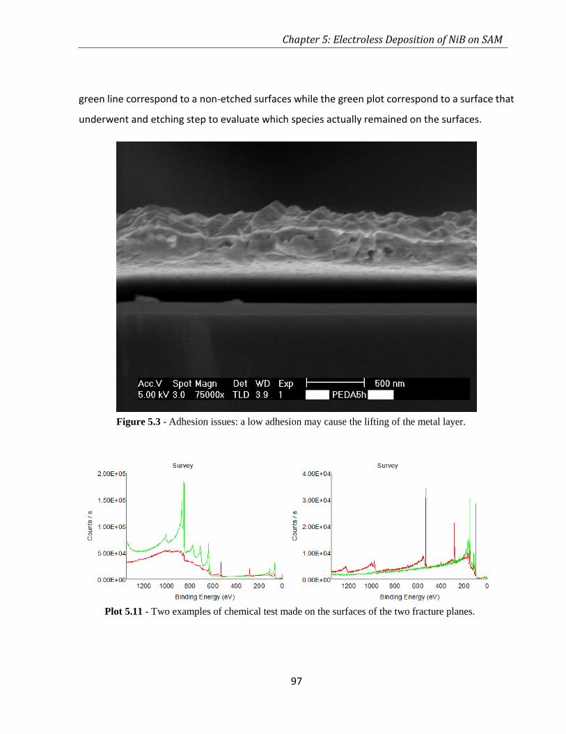
Chapter 5: Electroless Deposition of NiB on SAM
97
green line correspond to a non-etched surfaces while the green plot correspond to a surface that
underwent and etching step to evaluate which species actually remained on the surfaces.
Figure 5.3 - Adhesion issues: a low adhesion may cause the lifting of the metal layer.
Plot 5.11 - Two examples of chemical test made on the surfaces of the two fracture planes.
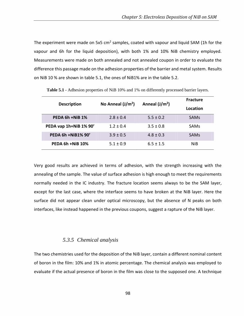
Chapter 5: Electroless Deposition of NiB on SAM
98
The experiment were made on 5x5 cm2 samples, coated with vapour and liquid SAM (1h for the
vapour and 6h for the liquid deposition), with both 1% and 10% NiB chemistry employed.
Measurements were made on both annealed and not annealed coupon in order to evaluate the
difference this passage made on the adhesion properties of the barrier and metal system. Results
on NiB 10 % are shown in table 5.1, the ones of NiB1% are in the table 5.2.
Table 5.1 - Adhesion properties of NiB 10% and 1% on differently processed barrier layers.
Description No Anneal (J/m2) Anneal (J/m2) Fracture
Location
PEDA 6h +NiB 1% 2.8 ± 0.4 5.5 ± 0.2 SAMs
PEDA vap 1h+NiB 1% 90’ 1.2 ± 0.4 3.5 ± 0.8 SAMs
PEDA 6h +NiB1% 90’ 3.9 ± 0.5 4.8 ± 0.3 SAMs
PEDA 6h +NiB 10% 5.1 ± 0.9 6.5 ± 1.5 NiB
Very good results are achieved in terms of adhesion, with the strength increasing with the
annealing of the sample. The value of surface adhesion is high enough to meet the requirements
normally needed in the IC industry. The fracture location seems always to be the SAM layer,
except for the last case, where the interface seems to have broken at the NiB layer. Here the
surface did not appear clean under optical microscopy, but the absence of N peaks on both
interfaces, like instead happened in the previous coupons, suggest a rapture of the NiB layer.
5.3.5 Chemical analysis
The two chemistries used for the deposition of the NiB layer, contain a different nominal content
of boron in the film: 10% and 1% in atomic percentage. The chemical analysis was employed to
evaluate if the actual presence of boron in the film was close to the supposed one. A technique
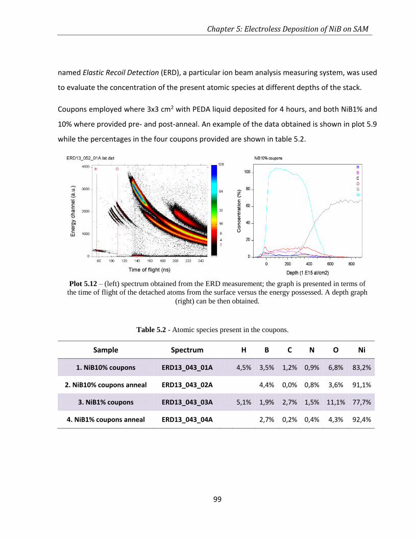
Chapter 5: Electroless Deposition of NiB on SAM
99
named Elastic Recoil Detection (ERD), a particular ion beam analysis measuring system, was used
to evaluate the concentration of the present atomic species at different depths of the stack.
Coupons employed where 3x3 cm2 with PEDA liquid deposited for 4 hours, and both NiB1% and
10% where provided pre- and post-anneal. An example of the data obtained is shown in plot 5.9
while the percentages in the four coupons provided are shown in table 5.2.
Table 5.2 - Atomic species present in the coupons.
Sample Spectrum H B C N O Ni
1. NiB10% coupons ERD13_043_01A
4,5% 3,5% 1,2% 0,9% 6,8% 83,2%
2. NiB10% coupons anneal ERD13_043_02A
4,4% 0,0% 0,8% 3,6% 91,1%
3. NiB1% coupons ERD13_043_03A
5,1% 1,9% 2,7% 1,5% 11,1% 77,7%
4. NiB1% coupons anneal ERD13_043_04A
2,7% 0,2% 0,4% 4,3% 92,4%
Plot 5.12 – (left) spectrum obtained from the ERD measurement; the graph is presented in terms of
the time of flight of the detached atoms from the surface versus the energy possessed. A depth graph
(right) can be then obtained.
As it can be seen from the tables, boron concentration is different when the 1% and 10% NiB
chemistry is used. The percentages of boron are anyway quite different from the expected
ones. The 1% NiB, with a quantity of 1.9% has a quite low boron quantity that is still higher
than the nominal one. This quantity increased after anneal, due to the high temperatures
reached when other chemical species are released. The NiB 10%, present a quantity that is a
third of the expected one before anneal and that goes up to 4.4% after the annealing step.
Carbon and hydrogen are nearly totally released after anneal and also the oxygen quantity
presents a strong decrease, giving rise to a good layer. The boron quantity is a factor directly
influencing the conductivity of the layer: since the different in the content is not as high as the
nominal value may suggest, it can be understood why the resistivity measured between the
NiB 10% and 1% is not so high either.
5.4 NiB in Trenches
5.4.1 Materials and Methods
The next step of the development of an alternative metal as interconnect is the actual
depositing and testing of the metal inside the conductive lines. Full wafer where provided, with
a single die patterned in many copies on it. The pattern of the die can be seen in figure 5.4.
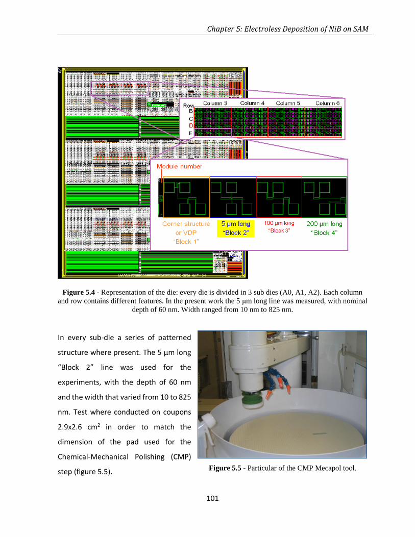
Chapter 5: Electroless Deposition of NiB on SAM
101
In every sub-die a series of patterned
structure where present. The 5 μm long
“Block 2” line was used for the
experiments, with the depth of 60 nm
and the width that varied from 10 to 825
nm. Test where conducted on coupons
2.9x2.6 cm2 in order to match the
dimension of the pad used for the
Chemical-Mechanical Polishing (CMP)
step (figure 5.5).
Figure 5.4 - Representation of the die: every die is divided in 3 sub dies (A0, A1, A2). Each column
and row contains different features. In the present work the 5 μm long line was measured, with nominal
depth of 60 nm. Width ranged from 10 nm to 825 nm.
Figure 5.5 - Particular of the CMP Mecapol tool.
Chapter 5: Electroless Deposition of NiB on SAM
102
Both SAMs where initially from a liquid phase for 2 and 5 hours, since these timings have been
proven to be useful in the previous experiments. PEDA and DETA where then used, coupled
with both NiB 1% and 10%. The deposition was carried out for several minutes, normmaly
aorund 45’, to give the possibility of a good metal film to deposit. A big deposit favour a more
precise CMP step. Once the deposition was made, the coupons where measured once, in order
to evaluate the line resistence pre-anneal, and then after anneal. The anneal step could not be
made after anneal due to delaminating events during the successive CMP progress. This was
probably casued by a variation in the chemical structure of the NiB that favoured a granular
structure; CMP was then made always pre-anneal. The CMP could be controlled easily thorugh
optical microscope during the polishing. To avoid the transmission of high stresses on the
metal thorugh the rotating pad the rotating speed was kept low and the pressure of the pad
was set on 2 psi; no cracking or delamination of the metal was seen in this case. The slurry
employed was based on the Acuplane 4100, normally employed for the polishing of nickel
alloys, it was very useful for the project due to its selectivity, during the polishing, of the metal
and not of the silica. The solution was composed by 2 L of water, 1 L of Acuplane 4100 with 15
ml of H2O2 needed to activate the chemical reactions happening during the polishing.
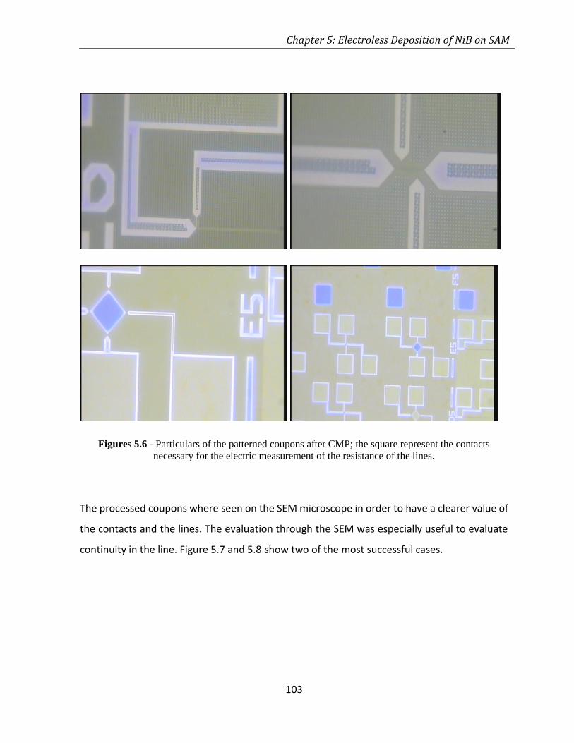
Chapter 5: Electroless Deposition of NiB on SAM
103
Figures 5.6 - Particulars of the patterned coupons after CMP; the square represent the contacts
necessary for the electric measurement of the resistance of the lines.
The processed coupons where seen on the SEM microscope in order to have a clearer value of
the contacts and the lines. The evaluation through the SEM was especially useful to evaluate
continuity in the line. Figure 5.7 and 5.8 show two of the most successful cases.
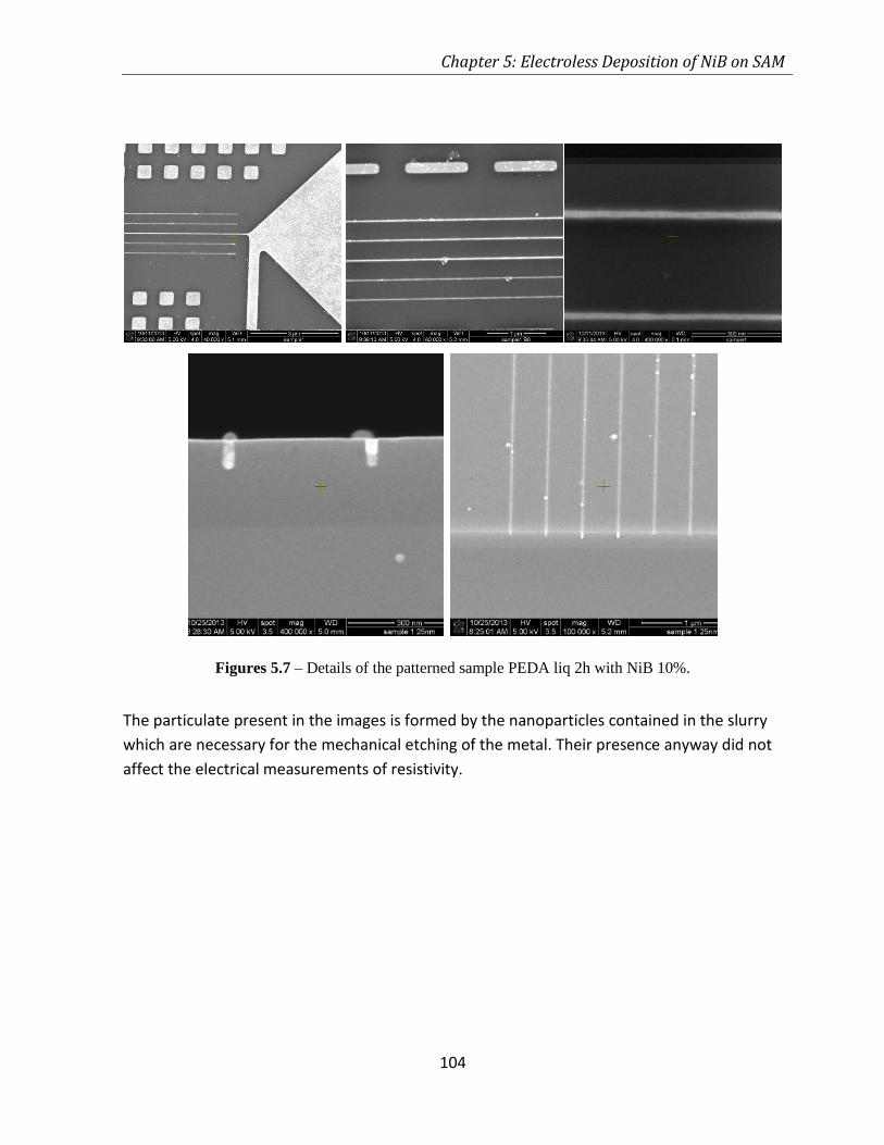
Chapter 5: Electroless Deposition of NiB on SAM
104
The particulate present in the images is formed by the nanoparticles contained in the slurry
which are necessary for the mechanical etching of the metal. Their presence anyway did not
affect the electrical measurements of resistivity.
Figures 5.7 – Details of the patterned sample PEDA liq 2h with NiB 10%.
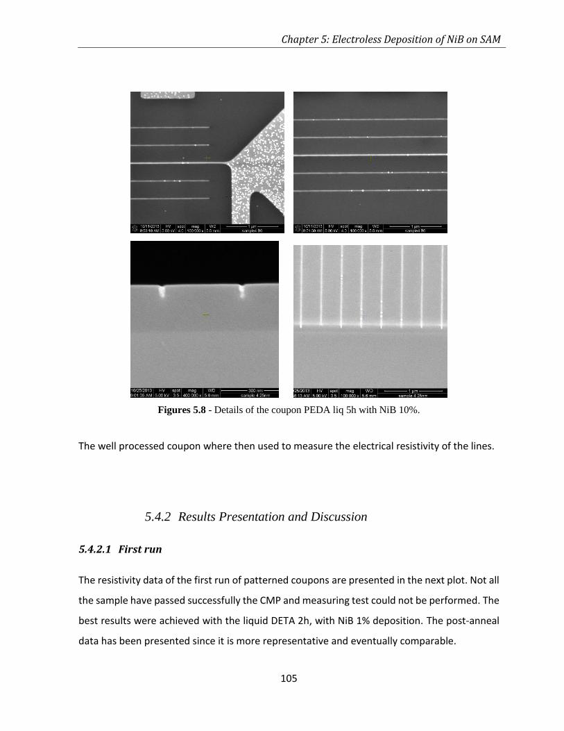
Chapter 5: Electroless Deposition of NiB on SAM
105
The well processed coupon where then used to measure the electrical resistivity of the lines.
5.4.2 Results Presentation and Discussion
5.4.2.1 First run
The resistivity data of the first run of patterned coupons are presented in the next plot. Not all
the sample have passed successfully the CMP and measuring test could not be performed. The
best results were achieved with the liquid DETA 2h, with NiB 1% deposition. The post-anneal
data has been presented since it is more representative and eventually comparable.
Figures 5.8 - Details of the coupon PEDA liq 5h with NiB 10%.
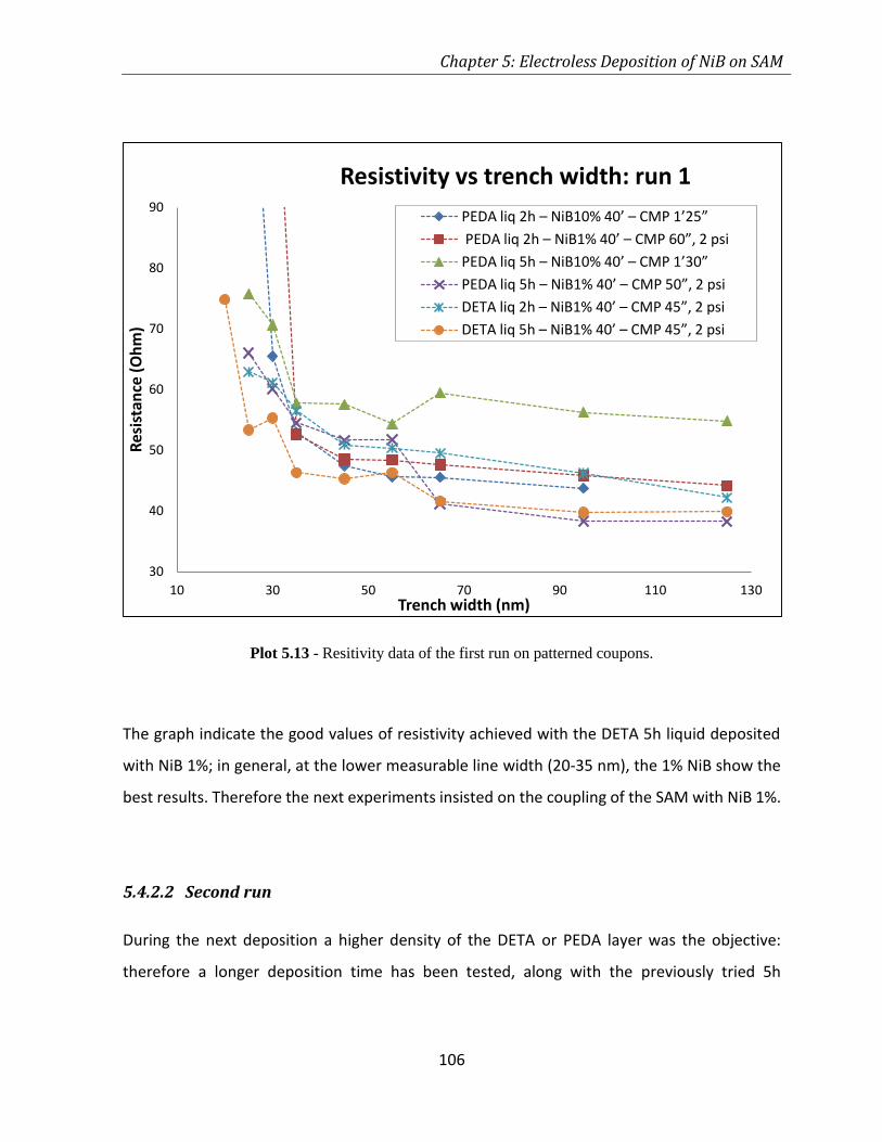
Chapter 5: Electroless Deposition of NiB on SAM
106
Plot 5.13 - Resitivity data of the first run on patterned coupons.
The graph indicate the good values of resistivity achieved with the DETA 5h liquid deposited
with NiB 1%; in general, at the lower measurable line width (20-35 nm), the 1% NiB show the
best results. Therefore the next experiments insisted on the coupling of the SAM with NiB 1%.
5.4.2.2 Second run
During the next deposition a higher density of the DETA or PEDA layer was the objective:
therefore a longer deposition time has been tested, along with the previously tried 5h
30
40
50
60
70
80
90
10 30 50 70 90 110 130
Res
ista
nce
(O
hm
)
Trench width (nm)
Resistivity vs trench width: run 1
PEDA liq 2h – NiB10% 40’ – CMP 1’25”
PEDA liq 2h – NiB1% 40’ – CMP 60”, 2 psi
PEDA liq 5h – NiB10% 40’ – CMP 1’30”
PEDA liq 5h – NiB1% 40’ – CMP 50”, 2 psi
DETA liq 2h – NiB1% 40’ – CMP 45”, 2 psi
DETA liq 5h – NiB1% 40’ – CMP 45”, 2 psi
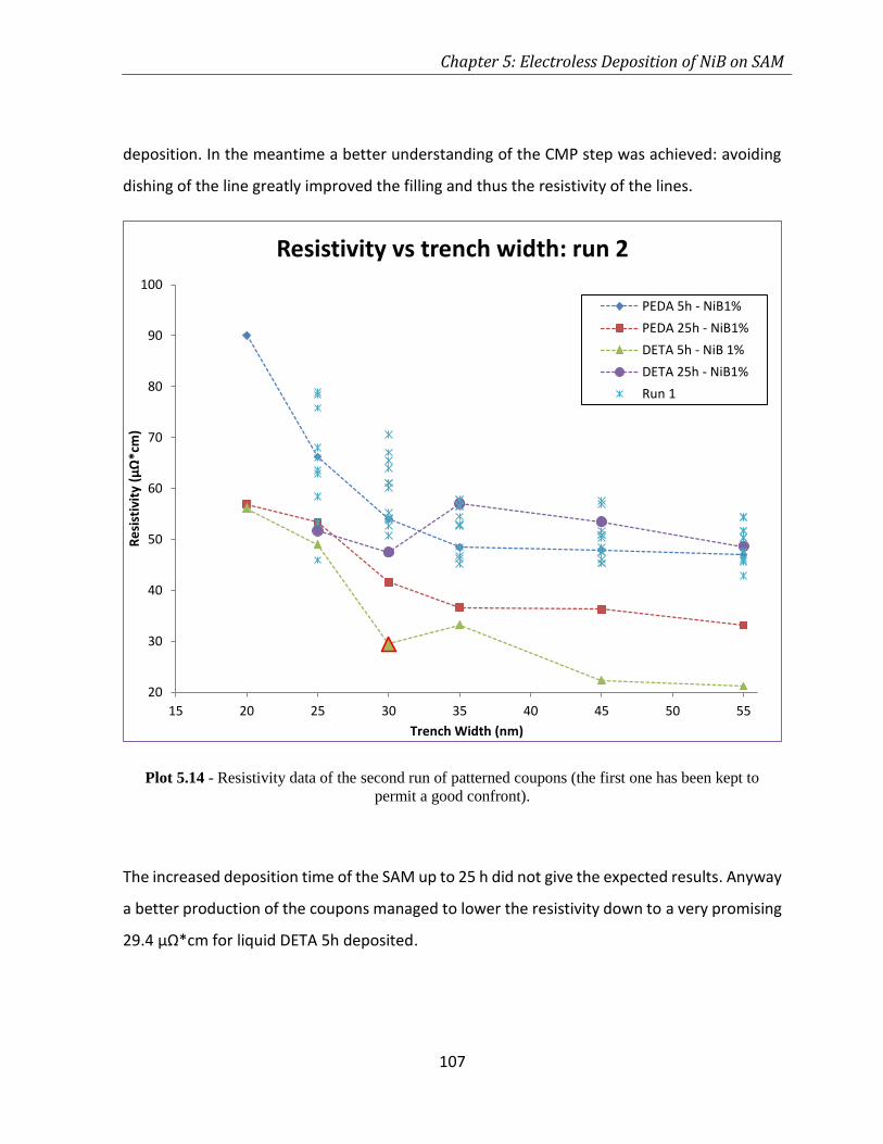
Chapter 5: Electroless Deposition of NiB on SAM
107
deposition. In the meantime a better understanding of the CMP step was achieved: avoiding
dishing of the line greatly improved the filling and thus the resistivity of the lines.
Plot 5.14 - Resistivity data of the second run of patterned coupons (the first one has been kept to
permit a good confront).
The increased deposition time of the SAM up to 25 h did not give the expected results. Anyway
a better production of the coupons managed to lower the resistivity down to a very promising
29.4 μΩ*cm for liquid DETA 5h deposited.
20
30
40
50
60
70
80
90
100
15 20 25 30 35 40 45 50 55
Re
sist
ivit
y (μ
Ω*c
m)
Trench Width (nm)
Resistivity vs trench width: run 2
PEDA 5h - NiB1%
PEDA 25h - NiB1%
DETA 5h - NiB 1%
DETA 25h - NiB1%
Run 1
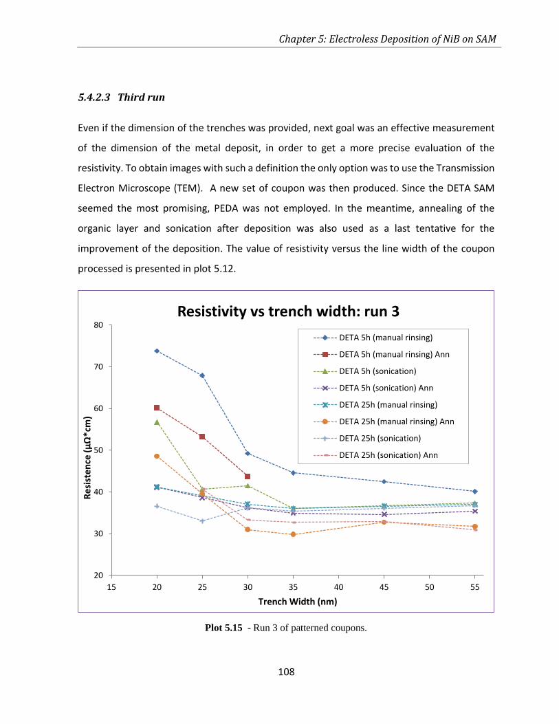
Chapter 5: Electroless Deposition of NiB on SAM
108
5.4.2.3 Third run
Even if the dimension of the trenches was provided, next goal was an effective measurement
of the dimension of the metal deposit, in order to get a more precise evaluation of the
resistivity. To obtain images with such a definition the only option was to use the Transmission
Electron Microscope (TEM). A new set of coupon was then produced. Since the DETA SAM
seemed the most promising, PEDA was not employed. In the meantime, annealing of the
organic layer and sonication after deposition was also used as a last tentative for the
improvement of the deposition. The value of resistivity versus the line width of the coupon
processed is presented in plot 5.12.
20
30
40
50
60
70
80
15 20 25 30 35 40 45 50 55
Re
sist
en
ce (
μΩ
*cm
)
Trench Width (nm)
Resistivity vs trench width: run 3
DETA 5h (manual rinsing)
DETA 5h (manual rinsing) Ann
DETA 5h (sonication)
DETA 5h (sonication) Ann
DETA 25h (manual rinsing)
DETA 25h (manual rinsing) Ann
DETA 25h (sonication)
DETA 25h (sonication) Ann
Plot 5.15 - Run 3 of patterned coupons.
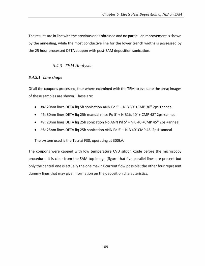
Chapter 5: Electroless Deposition of NiB on SAM
109
The results are in line with the previous ones obtained and no particular improvement is shown
by the annealing, while the most conductive line for the lower trench widths is possessed by
the 25 hour processed DETA coupon with post-SAM deposition sonication.
5.4.3 TEM Analysis
5.4.3.1 Line shape
Of all the coupons processed, four where examined with the TEM to evaluate the area; images
of these samples are shown. These are:
#4: 20nm lines DETA liq 5h sonication ANN Pd 5' + NiB 30' +CMP 30'' 2psi+anneal
#6: 30nm lines DETA liq 25h manual rinse Pd 5’ + NiB1% 40’ + CMP 48” 2psi+anneal
#7: 20nm lines DETA liq 25h sonication No ANN Pd 5' + NiB 40'+CMP 45'' 2psi+anneal
#8: 25nm lines DETA liq 25h sonication ANN Pd 5' + NiB 40'-CMP 45''2psi+anneal
The system used is the Tecnai F30, operating at 300kV.
The coupons were capped with low temperature CVD silicon oxide before the microscopy
procedure. It is clear from the SAM top image (figure that five parallel lines are present but
only the central one is actually the one making current flow possible; the other four represent
dummy lines that may give information on the deposition characteristics.
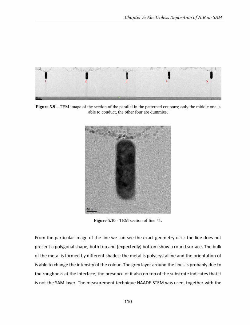
Chapter 5: Electroless Deposition of NiB on SAM
110
From the particular image of the line we can see the exact geometry of it: the line does not
present a polygonal shape, both top and (expectedly) bottom show a round surface. The bulk
of the metal is formed by different shades: the metal is polycrystalline and the orientation of
is able to change the intensity of the colour. The grey layer around the lines is probably due to
the roughness at the interface; the presence of it also on top of the substrate indicates that it
is not the SAM layer. The measurement technique HAADF-STEM was used, together with the
Figure 5.9 – TEM image of the section of the parallel in the patterned coupons; only the middle one is
able to conduct, the other four are dummies.
Figure 5.10 - TEM section of line #1.
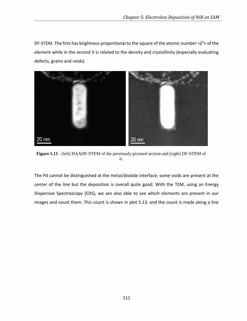
Chapter 5: Electroless Deposition of NiB on SAM
111
DF-STEM. The first has brightness proportional to the square of the atomic number <Z2> of the
element while in the second it is related to the density and crystallinity (especially evaluating
defects, grains and voids).
The Pd cannot be distinguished at the metal/dioxide interface; some voids are present at the
center of the line but the deposition is overall quite good. With the TEM, using an Energy
Dispersive Spectroscopy (EDS), we are also able to see which elements are present in our
images and count them. This count is shown in plot 5.13, and the count is made along a line
Figure 5.11 - (left) HAADF-STEM of the previously pictured section and (right) DF-STEM of
it.
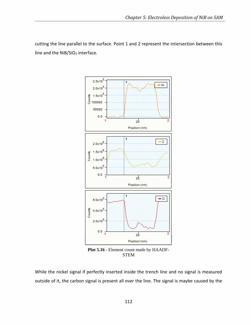
Chapter 5: Electroless Deposition of NiB on SAM
112
cutting the line parallel to the surface. Point 1 and 2 represent the intersection between this
line and the NiB/SiO2 interface.
While the nickel signal if perfectly inserted inside the trench line and no signal is measured
outside of it, the carbon signal is present all over the line. The signal is maybe caused by the
Plot 5.16 - Element count made by HAADF-
STEM
Chapter 5: Electroless Deposition of NiB on SAM
113
plasma etch step necessary to clean the sample before the measuring step. An intensity peak
is not evident at the interface where the SAM layer should be but this is might be due to a not
high enough lateral resolution or the destruction of the SAM during the plasma etching step.
5.4.3.2 Line resistivity
The sections of the four conductive lines are shown in figure 5.10: we will now use this
additional information to evaluate the resistivity of the samples.
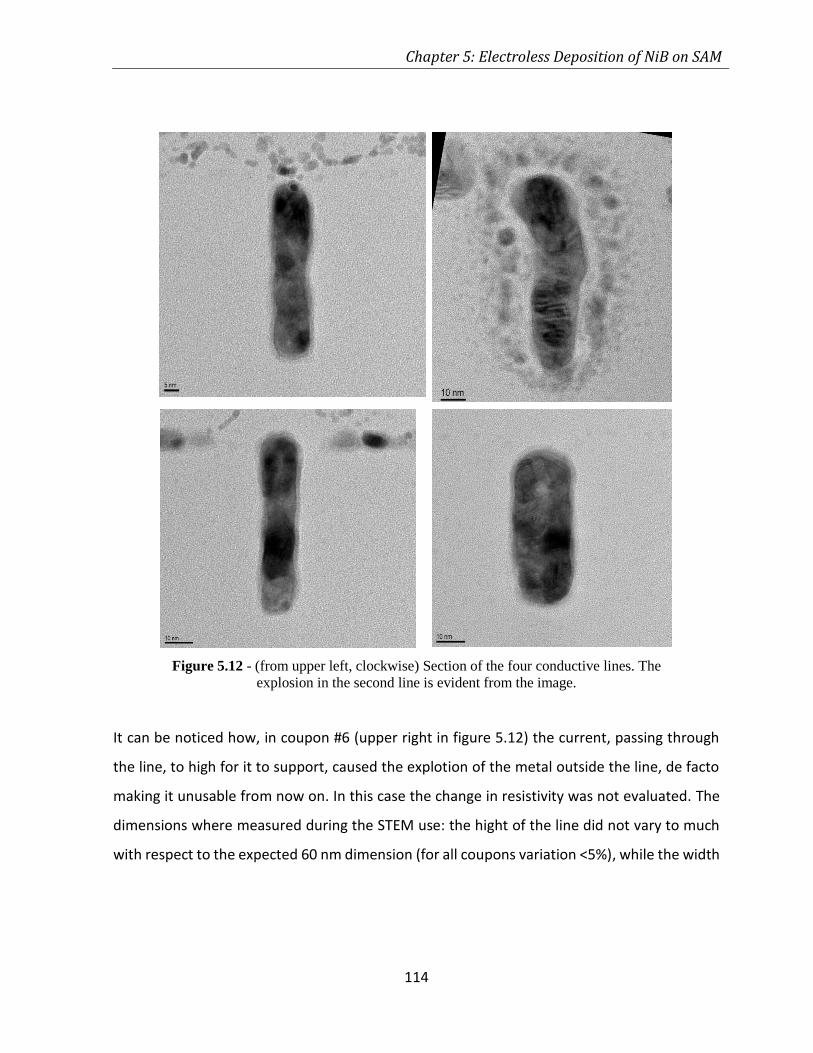
Chapter 5: Electroless Deposition of NiB on SAM
114
It can be noticed how, in coupon #6 (upper right in figure 5.12) the current, passing through
the line, to high for it to support, caused the explotion of the metal outside the line, de facto
making it unusable from now on. In this case the change in resistivity was not evaluated. The
dimensions where measured during the STEM use: the hight of the line did not vary to much
with respect to the expected 60 nm dimension (for all coupons variation <5%), while the width
Figure 5.12 - (from upper left, clockwise) Section of the four conductive lines. The
explosion in the second line is evident from the image.
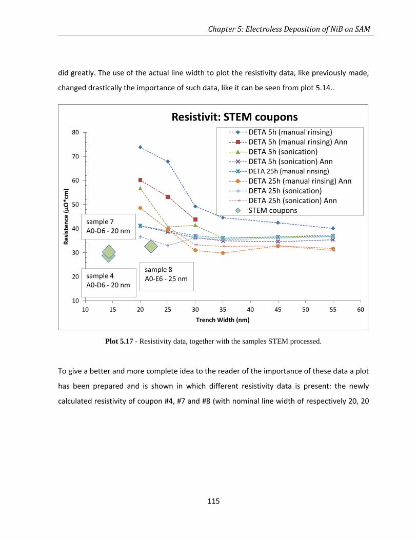
Chapter 5: Electroless Deposition of NiB on SAM
115
did greatly. The use of the actual line width to plot the resistivity data, like previously made,
changed drastically the importance of such data, like it can be seen from plot 5.14..
To give a better and more complete idea to the reader of the importance of these data a plot
has been prepared and is shown in which different resistivity data is present: the newly
calculated resistivity of coupon #4, #7 and #8 (with nominal line width of respectively 20, 20
10
20
30
40
50
60
70
80
10 15 20 25 30 35 40 45 50 55 60
Re
sist
en
ce (
μΩ
*cm
)
Trench Width (nm)
Resistivit: STEM couponsDETA 5h (manual rinsing)DETA 5h (manual rinsing) AnnDETA 5h (sonication)DETA 5h (sonication) AnnDETA 25h (manual rinsing)
DETA 25h (manual rinsing) AnnDETA 25h (sonication)DETA 25h (sonication) AnnSTEM coupons
sample 7A0-D6 - 20 nm
sample 4A0-D6 - 20 nm
sample 8A0-E6 - 25 nm
Plot 5.17 - Resistivity data, together with the samples STEM processed.
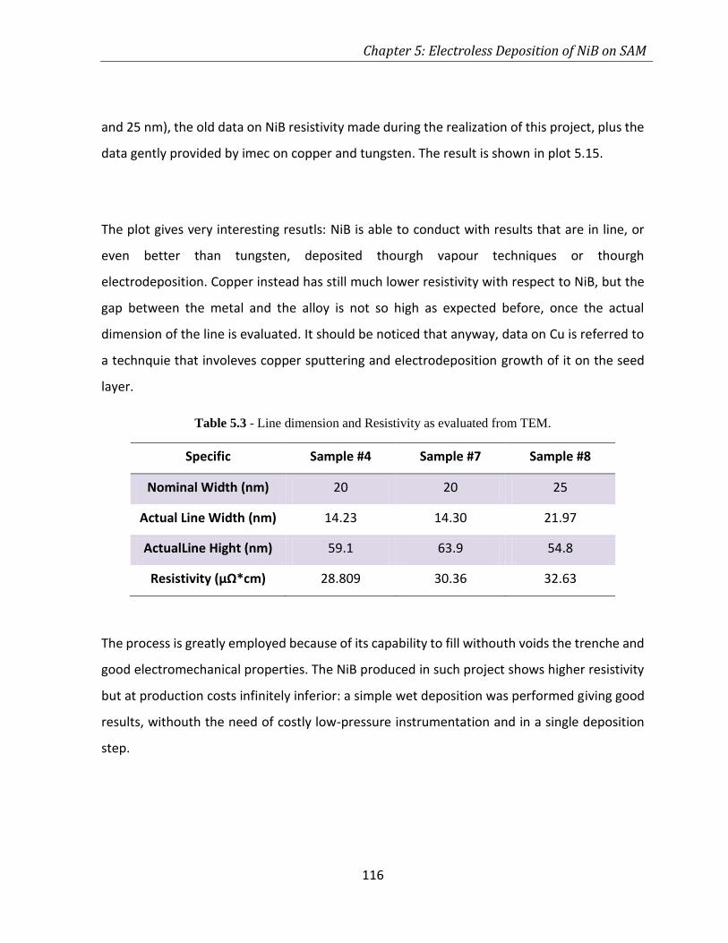
Chapter 5: Electroless Deposition of NiB on SAM
116
and 25 nm), the old data on NiB resistivity made during the realization of this project, plus the
data gently provided by imec on copper and tungsten. The result is shown in plot 5.15.
The plot gives very interesting resutls: NiB is able to conduct with results that are in line, or
even better than tungsten, deposited thourgh vapour techniques or thourgh
electrodeposition. Copper instead has still much lower resistivity with respect to NiB, but the
gap between the metal and the alloy is not so high as expected before, once the actual
dimension of the line is evaluated. It should be noticed that anyway, data on Cu is referred to
a technquie that involeves copper sputtering and electrodeposition growth of it on the seed
layer.
Table 5.3 - Line dimension and Resistivity as evaluated from TEM.
Specific Sample #4 Sample #7 Sample #8
Nominal Width (nm) 20 20 25
Actual Line Width (nm) 14.23 14.30 21.97
ActualLine Hight (nm) 59.1 63.9 54.8
Resistivity (μΩ*cm) 28.809 30.36 32.63
The process is greatly employed because of its capability to fill withouth voids the trenche and
good electromechanical properties. The NiB produced in such project shows higher resistivity
but at production costs infinitely inferior: a simple wet deposition was performed giving good
results, withouth the need of costly low-pressure instrumentation and in a single deposition
step.

Chapter 5: Electroless Deposition of NiB on SAM
117
The most important objective,reached in this section, is that the deposition of NiB through ELD
is not only possible but it can be easily achieved in lines as small as 12 nm, with remarkable
conductivity properties.
Chapter 6: Conclusions and Future Perspectives
118
Chapter 6: Conclusions and
Future Perspectives
6.1 Conclusions
As the shrinking of the characteristic dimensions of nodes and interconnections continues in
the IC industry it is by now clear that the Ta/TaN layer will not be able guarantee good step
coverage and anti-diffusion properties for thicknesses below 5 nm.
Self-assembled monolayer, embedded in a SiO2/NiB stack, appears as a strong candidate for
the substitution of obsolete barrier layers, due to their structural and chemical properties
allowing them to have good barrier properties and provide a suitable substrate for subsequent
depositions. To realize such sandwiched structure, an “all-wet” process has been under
examination in this work.
The first part of the project was focused on the screening of two different SAM precursor
molecules, with varying deposition process specifics. Along with the commonly used liquid
deposition, a vapour deposition was also explored in a first attempt for the scaling-up of the
current “all-wet” process to full wafer. The SAMs layers were characterized through the
evaluation of different properties in order to achieve an overall better deposition in terms of:
structural density and thicknesses;
formation of a monolayer;
surface amino- groups.
A Langmuir-type growth was observed for both DETA and PEDA deposited from solution. Low
thicknesses (<2 nm) where reached with good densities (especially for liquid PEDA) just after
Chapter 6: Conclusions and Future Perspectives
119
2 hours deposition, with the packing of the molecules increasing with longer deposition times.
But if for PEDA, the maximum amount of nitrogen surface atoms (directly related to the
amount of amino-groups present) reaches 3.5% after 5 hours of liquid deposition, the DETA
SAM, despite the higher amount of amino groups possessed by the precursor (3, against the 2
of PEDA), shows a lower quantity of surface N atoms: 2.64%. On the contrary vapour DETA
manages to reach values as high as 5.31% for a 30’ deposit, confirming promising outlook.
PEDA instead does not show good properties for a vapour deposition. Results are confirmed
by XPS, where the amount of Pd-catalyser deposited over the organic layer, whose quantity
and homogeneity directly affects the metal deposit properties, is higher for the vapour DETA
(91.4*1013), in the case of liquid deposition, and the 5 hours liquid PEDA (36*1013). PEDA
confirms to be a highly packed organic layer, thanks to the bulky benzene ring present in the
backbone and a very good substrate for Pd liquid uptake. Vapour DETA appears promising but
a better understanding of vapour deposition should be achieved to perfectly understand the
organic layer formation mechanism and the deposit quality.
After analysing the organic layer deposition step and the palladium uptake on different
substrates, the metal electroless deposition was taken into account. The PdCl2-based solution
and the two NiB chemistry employed in the research were provided by LAM Research®. A
different amount of boron is contained in the two deposits due to different bath composition,
with nominal quantity of 10% and 1%. Since the two chemistries are not commercial, no
precise knowledge of the composition of them is perfectly known. Resistivity was calculated
for thin film deposition of both NiB 1% and 10% on variously deposited organic layer. The
annealing of the SAM did not bring any change in the deposit quality and was therefore
abandoned to avoid the risk of contamination. The metal annealing, providing the possibility
of crystalline reorganization, confirmed a drop of one order of magnitude of the thin film
resistivity. NiB 1% gave the best result especially on 5 hours long processed liquid PEDA and
DETA (respectively min=30÷40 µΩ*cm for film thicknesses around 20 nm and min=35÷45
µΩ*cm for thicknesses around 15nm) and on vapour PEDA min=21÷23 µΩ*cm for 20 nm and
Chapter 6: Conclusions and Future Perspectives
120
65÷70 µΩ*cm for 10 nm). Other measurements confirmed a not expected faster growth rate
of 1% with respect to the 10% (the higher quantity of reducing agent in NiB 10% should be
responsible for a faster deposition of the metal). Also, adhesion confirmed to be high enough
to exceed the requirements for successive processing in the IC industry with values up to 6.5
J/m2. ERD confirmed a different composition of the bath from the deposit, with NiB 1% film
containing slightly more than expected B (2,7% after anneal) and NiB 10% containing much
less (4,4%) than the nominal 10%.
Since better knowledge is possessed on liquid SAM deposition and, at the same time, vapour
deposition is known not to have good homogeneity over full wafer and good step coverage
still have to be confirmed, only liquid deposited SAM was used on patterned coupons. Line
resistivity was measured employing both chemistry, even if NiB 10% was promptly abandoned
due to the lower conductive properties compared to the NiB 1%. NiB was deposited up to circa
300 nm in order to completely fill the trenches and features present in the coupons and easing
the successive CMP step. After a better knowledge of this latter step was achieved, through
experience and through the use of optical microscopy and SEM, the best result where reached
on liquid 5h DETA deposited, with a resistivity of 29.4 μΩ*cm on a 30 nm wide line. Longer
deposition, coupled with sonication cleaning did not give a remarkable decrease in resistivity,
but, of this last run, the four better resulting coupons where given for TEM analysis. The TEM
confirmed the barrier ability of the organic layer between NiB and SiO2, with good filling of the
line. A rough interface and the presence of different grains are confirmed by the high
resolution images. Also, it is evident that shape and dimensions of the line is not the one
expected: the section possesses a round top and bottom and width appears to be much smaller
(height is more or less the same). A new evaluation of the section, coupled with the
modification of the already calculated resistivity, gave the remarkable result of 28 µΩ*cm for
a line width of 14 nm. The gap between copper and NiB appear still quite large but the
deposition shows important promising characteristics. A part from a resistivity in line, or even
lower, with all the other metals normally employed in IC industry (like W), the process has the
Chapter 6: Conclusions and Future Perspectives
121
great advantage of employing very cheap deposition techniques. Besides, no, or limited (in the
case of vapour SAM deposition), use of high vacuum processes, like instead traditional
processes like sputtering or CVD/PVD, is required. Therefore ELD NiB on SAM can be
considered a good alternative to the currently employed PVD/sputtering Ta/TaN barrier.
6.2 Future Perspectives
It would be impossible in just a few lines to address the infinite possible perspectives of
integrated circuits in ULSI technology. Thus, only the possibilities of SAM organic layers
coupled with ELD metals will be treated. To complete the current project a better study on the
metal annealing step should be taken: the fact that the CMP step works easily pre-anneal but
not after it implies a change in the chemical and physical structure of it. A change in the phases
and/or grain dimension could be the cause, but an accurate XRD test is probably needed to
actually demonstrate it. A better understanding of the bath could give insight on the
composition and could explain why the composition of the film are different from the nominal
one and why the growth rates show inverted values (faster for NiB 1% which contains a lower
quantity of reduction agent). Finally a better filling of the line (voids may be caused by the
rearrangement of the increasing grain size) should be achieved in order to get lower resistivity
values.
Considering a more long-term research, a better understanding of the vapour deposition
mechanism of amino-silanes would bring essential advancements in the scaling up process
from coupons to full-wafer. This is an essential step necessary for the process to be developed
for an industrial application. Other terminating group could also be studied and employed: i.e.
pyridines, azido-compounds, metalphtalocyanines. Maybe coupled with alternative catalysers
like copper, tin or other noble metal nanoparticles. It would be interesting to evaluate the

Chapter 6: Conclusions and Future Perspectives
122
coupling of SAM with other ELD metals. Deposition of pure Ni instead of an alloy would surely
bring better conduction properties. Different metals could be deposited, like cobalt (Co),
transitional metals, like Rhodium (Rh) or Ruthenium (Ru) or even silver (Ag).
References
123
References
1. Feynman, R. P. Plenty of room at the bottom. in Talk to Am. Phys. Soc. 1–7 (1959).
2. Taniguchi, N. On the Basic Concept of “Nano-Technology.”in Proc. Int. Conf. Prod. Eng. (1974).
3. Ramsden, J. Essentials of nanotechnology. 126 (2009).
4. Foresight Institute - About Nanotechnology. at <https://www.foresight.org/nano/>
5. Haselman, M. & Hauck, S. The future of integrated circuits: A survey of nanoelectronics. Proc. IEEE 1–57 (2010).
6. International Technology Roadmap for Semiconductors (2005 Edition). (2005). at <http://scholar.google.com/scholar?hl=en&btnG=Search&q=intitle:INTERNATIONAL+TECHNOLOGY+ROADMAP+FOR+semiconductors+2005+edition#1>
7. Rodgers, P. Nanoelectronics: Single file. Nat. Nanotechnol. (2006). doi:10.1038/nnano.2006.5
8. Tseng, A. A., Cheng, K., Chen, C. D. & Ma, K. J. IEEE Transaction on Electronics Packaging Manufacturing. IEEE (2003).
9. George, S. M., Ott, A. W. & Klaus, J. W. Surface Chemistry for Atomic Layer Growth. J. Phys. Chem. 100, 31 (1996).
10. George, S. M., Yoon, B. & Dameron, A. A. Surface Chemistry for Molecular Layer Deposition of Organic and Hybrid Organic-Inorganic Polymers. Acc. Chem. Res. 42, 498 (2008).
11. Gin, A., Movaghar, B., Razeghi, M. & Brow, G. J. Infrared detection from GaInAs/InP nanopillar arrays. Nanotechnol. 16 (2005).
12. IBM100 - Copper Interconnects: The Evolution of Microprocessors. (IBM Corporation, 2012).
References
124
13. Andricacos, P. C. Copper on-chip interconnections, a breakthrough in electrodeposition to make better chips. Electrochem. Soc. Iterface 32–37 (1999).
14. Campbell, S. The science and engineering of microelectronic fabrication. 2nd Ed. Oxford university Press (2001).
15. Andricacos, P. C., Uzoh, C., Dukovic, J. O., Horkans, J. & Deligianni, H. Damascene copper electroplating for chip interconnections. IBM J. Res. Dev. 42, 567–574 (1998).
16. Pallinti, J. & Lakshminarayanan, S. An overview of stress free polishing of Cu with ultra low-k (k< 2.0) films. Interconnect Technol. Conf. 83–85 (2003).
17. Pratt, A. Overview of the use of copper interconnects in the semiconductor industry. Adv Energy Ind (2004).
18. Gupta, T. Copper interconnect technology. (2009).
19. Intel’s 14nm milkshake: It’s better than yours. at <http://www.extremetech.com/computing/171477-intels-14nm-milkshake-its-better-than-yours>
20. Istratov, A., Flink, C., Hieslmair, H., Weber, E. & Heiser, T. Intrinsic Diffusion Coefficient of Interstitial Copper in Silicon. Phys. Rev. Lett. 81, 1243–1246 (1998).
21. Cros, a., Aboelfotoh, M. O. & Tu, K. N. Formation, oxidation, electronic, and electrical properties of copper silicides. J. Appl. Phys. 67, 3328 (1990).
22. McBrayer, J. D., Swanson, R. M. & Sigmon, T. W. Diffusion of Metals in Silicon Dioxide. J. Electrochem. Soc. 133, 1242–1246 (1986).
23. Murarka, S. P. Copper – Fundamental Mechanisms for Microelectronic Applications. (1989).
24. Baklanov, M., Ho, P. S. & Zschech, E. Advanced Interconnects for ULSI Technology. 579 (2012).
25. Nicolet, M. & Bartur, M. Diffusion barriers in layered contact structures. J. Vac. Sci. Technol. 19, 786–793 (1981).
26. Li, B., Sullivan, T. D., Lee, T. C. & Badami, D. Reliability challenges for copper interconnects. Microelectron. Reliab. 44, 365–380 (2004).
References
125
27. Rathore, H., Aganvala, B. & Nguyen, D. A high performance liner for copper damascene interconnects. Interconnect Technol. Conf. 2001. Proc. IEEE 2001 Int. 9–11 (2001).
28. Fischer, a C. et al. Very high aspect ratio through-silicon vias (TSVs) fabricated using automated magnetic assembly of nickel wires. J. Micromechanics Microengineering 22, 105001 (2012).
29. Kim, H., Kellock, A. J. & Rossnagel, S. M. Growth of cubic-TaN thin films by plasmaenhanced atomic layer deposition. J. Appl. Phys. 92, 7080–7085 (2002).
30. Fayolle, M., Passemard, G. & Louveau, O. Challenges of back end of the line for sub 65 nm generation. Microelectron. … 70, 255–266 (2003).
31. Wang, K., Horsfall, A., Cuthbertson, A., Bull, S. & O’Neill, A. Comparative study of novel barrier layers in ULSI copper interconnects. Microelectron. Eng. 84, 2486–2490 (2007).
32. Dubin, V. M. Scaling Trends and Advances in Metal Technologies for On-Chip Interconnects. 4 (2003).
33. Li, W. Atomic layer deposition methods for forming a multi-layer adhesion-barrier layer for integrated circuits. US Pat. 6,955,986 2, (2005).
34. Chaudhry, A. Interconnects for nanoscale MOSFET technology: a review. J. Semicond. 34, 066001 (2013).
35. Kioussis, D. et al. Optimization of Porous Ultra Low- κ Dielectrics ( κ ≤ 2 . 55 ) for 28nm Generation. 2–4 (2011).
36. Caro, A. M. Exploration of SAMs (self - assembled monolayers) in advanced interconnects. IMEC-KUL, (2012).
37. Barlow, S. M. & Raval, R. Complex organic molecules at metal surfaces: bonding, organisation and chirality. Surf. Sci. Rep. 50, 201–341 (2003).
38. Schreiber, F. Structure and growth of self-assembling monolayers. Prog. Surf. Sci. 65, 151–257 (2000).
39. Franklin, B., Brownrigg, W. & Farish, M. Of the Stilling of Waves by means of Oil. Extracted from Sundry Letters between Benjamin Franklin, LL. D. F. R. S. William Brownrigg, M. D. F. R. S. and the Reverend Mr. Farish. Philos. Trans. R. Soc. London 64, 445–460 (1774).
References
126
40. Pockels, A. Nature 43, 437 (1891).
41. Pockels, A. Nature 46, 418 (1892).
42. Pockels, A. Nature 50, 223 (1894).
43. Rayleigh, L. Phylosophic Mag. 48, 321 (1899).
44. Hardy, W. B. Proc. R. Soc. London A 86, 610 (1912).
45. Langmuir, I. The Faraday Society. Trans. Faraday Soc. 17, (1920).
46. Blodgett, K. B. Films built by depositing successive monomolecular layers on a solid surface. J. Am. Chem. Soc. 621, 1007–1022 (1935).
47. Love, J. C., Estroff, L. A., Kriebel, J. K., Nuzzo, R. G. & Whitesides, G. M. Chem. Rev. Chem. Rev. 105, 1103 (2005).
48. Love, J. C., Estroff, L. a, Kriebel, J. K., Nuzzo, R. G. & Whitesides, G. M. Self-assembled monolayers of thiolates on metals as a form of nanotechnology. Chem. Rev. 105, 1103–69 (2005).
49. Janssen, D. Self-assembling monolayers for organic thin-film transistors. (2006). at <https://lirias.kuleuven.be/handle/1979/330>
50. Ishida, T. et al. J. Phys. Chem. 106, 23, 5886 (2002).
51. Bhushan, B. Principles and Applications of Tribology. (John Wiley & Sons, Inc., 1999).
52. Maboudian, R., Ashurst, W. R. & Carraro, C. Self-assembled monolayers as anti-stiction coatings for MEMS: characteristics and recent developments. Sensors Actuators A Phys. 82, 219–223 (2000).
53. Srinivasan, U., Houston, M. R., Howe, R. T. & Maboudian, R. Alkyltrichlorosilane-based self-assembled monolayer films for stiction reduction in silicon micromachines. J. Microelectromechanical Syst. 7, 252–260 (1998).
54. Xiang, H. & Komvopoulos, K. Effect of fluorocarbon self-assembled monolayer films on sidewall adhesion and friction of surface micromachines with impacting and sliding contact interfaces. J. Appl. Phys. 113, 224505 (2013).
References
127
55. Maboudian, R., Ashurst, W. R. & Carraro, C. Tribological challenges in micromechanical systems. Tribol. Lett. 12, 95–100 (2002).
56. Xu, G., Bao, Z. & Groves, J. Langmuir-Blodgett films of regioregular poly (3-hexylthiophene) as field-effect transistors. Langmuir 1834–1841 (2000).
57. Collet, J., Bonnier, M., Bouloussa, O., Rondelez, F. & Vuillaume, D. Microelectron. Eng. 36, 119 (1997).
58. Sakuma, H., Iizuka, M., Nakamura, M., Kudo, K. & Tanaka, K. Fabrication of Field-Effect Transistor Using Charge-Transfer-Complex Langmuir-Blodgett Films. Jpn. J. Appl. Phys. 41, 2727–2729 (2002).
59. Gee, M. L., Healy, T. W. & White, L. R. Hydrophobicity effects in the condensation of water films on quartz. J. Colloid Interface Sci. 140, 450–465 (1990).
60. Vigil, G., Xu, Z., Steinberg, S. & Israelachvili, J. Interactions of Silica Surfaces. J. Colloid lnterface Sci. 165, 367–385 (1994).
61. Krishnamoorthy, A., Chanda, K., Murarka, S. P., Ramanath, G. & Ryan, J. G. Self-assembled near-zero-thickness molecular layers as diffusion barriers for Cu metallization. Appl. Phys. Lett. 78, 2467–2469 (2001).
62. Bishop, A. R. & Nuzzo, R. G. Self-assembled monolayers: Recent developments and applications. Curr. Opin. Colloid Interface Sci. 1, 127–136 (1996).
63. Sung, M. & Kim, Y. Self-assembled monolayers of alkanethiols on clean copper surfaces. Bull. Chem. Soc. 22, 748–752 (2001).
64. Mikami, N., Hata, N., Kikkawa, T. & Machida, H. Robust self-assembled monolayer as diffusion barrier for copper metallization. Appl. Phys. Lett. 83, 5181 (2003).
65. Ramanath, G. et al. Self-assembled subnanolayers as interfacial adhesion enhancers and diffusion barriers for integrated circuits. Appl. Phys. Lett. 83, 383 (2003).
66. Ganesan, P. G., Singh, a. P. & Ramanath, G. Diffusion barrier properties of carboxyl- and amine-terminated molecular nanolayers. Appl. Phys. Lett. 85, 579 (2004).
67. Gandhi, D. D. et al. Molecular-nanolayer-induced suppression of in-plane Cu transport at Cu-silica interfaces. Appl. Phys. Lett. 90, 163507 (2007).
References
128
68. Gandhi, D. D. et al. Annealing-induced interfacial toughening using a molecular nanolayer. Nature 447, 299–302 (2007).
69. Maestre Caro, a., Maes, G., Borghs, G. & Whelan, C. M. Screening self-assembled monolayers as Cu diffusion barriers. Microelectron. Eng. 85, 2047–2050 (2008).
70. Caro, A. M. et al. High Quality NH2SAM (Self Assembled Monolayer) Diffusion Barrier for Advanced Copper Interconnects. MRS Proc. 1249, F02–01 (2010).
71. Caro, A. M. et al. Bottom-Up Engineering of Subnanometer Copper Diffusion Barriers Using NH2-Derived Self-Assembled Monolayers. Adv. Funct. Mater. 20, 1125–1131 (2010).
72. Carnevali, G. Self-assembled monolayers for electroless metallization in TSV integration. (2013).
73. Parikh, A. & Allara, D. An intrinsic relationship between molecular structure in self-assembled n-alkylsiloxane monolayers and deposition temperature. J. Phys. Chem. 98, 7577–7590 (1994).
74. Chailapakul, O. & Sun, L. Interactions between organized, surface-confined monolayers and vapor-phase probe molecules. 7. Comparison of self-assembling n-alkanethiol monolayers. J. Am. Chem. Soc. 115, 12459–12467 (1993).
75. Djokic, S. S. & Cavallotti, P. L. in Electroless Depos. Theory Pract. 252 (2010).
76. Hajdu, G. O., Hajdu, M. & Hajdu, J. B. Electroless Plating: Fundamentals and Applications. Am. Electroplat. Surf. Finischers Soc. (1990).
77. Schlesinger, M. Electroless Deposition of Nickel, in Modern Electroplating, Fifth Edition. (2011).
78. Shacham-Diamond, Y., Dubin, V. M. & Argyal, M. Thin Solid Film. 262, 93 (1995).
79. Dubin, V. M., Shacham-Diamond, Y., Zhao, B., Vasudev, P. K. & Ting, C. H. Journal of The Electrochemical Society. J. Electrochem. Soc. 144, 93 (1997).
80. Bindra, P. & White, J. R. in Electroless Plat. - Fundam. Appl. (Publishing/Noyes, W. A.) 289 (1990).
81. Gorbunova, K., Ivanov, M. & Moiseev, V. Journal of Electrochemical Society. 120, 613 (1973).
References
129
82. Mallory, G. Plating. 58, 319 (1971).
83. Cavallotti, P. L. & Salvago, G. Electrochimica Metalli. 3, 239 (1968).
84. Novotortseva, I. G., Gaevskaya, T. V. & Tsybulskaya, L. S. Bulletin of Belarussian State University. 2, 16–20 (1994).
85. Gaevskaya, T. V., Novotortseva, I. G. & Tsybulskaya, L. S. Russian Journal of Applied Chemistry. 68, 587–592 (1995).
86. Novotortseva, I. G., Gaevskaya, T. V. & Tsybulskaya, L. S. Izvestiya Belarussian Academy of Sciences. Ser. Chem. Sci. 49–54 (1995).
87. Novotortseva, I. G. & Gaevskaya, T. V. Inorganic Materials. 31, 1053–1058 (1995).
88. Rao, Q., Bi, G., Lu, Q., Wang, H. & Fan, X. Microstructure evolution of electroless Ni-B film during its depositing process. Appl. Surf. Sci. 240, 28–33 (2005).
89. Ohno, I., Wakabayashi, O. & Haruyama, S. Denki Kagaku. 53, 190 (1985).
90. Shipley, C. R. J. U. S. Pat. 3011920 (1961).
91. O’Sullivan, E. J. et al. Electrolessly deposited diffusion barriers for microelectronics. IBM J. Res. Dev. 42, 607–620 (1998).
92. Takano, N., Kurokawa, T., Osaka, T. & Kazuyoshi, U. Electroless Nickel Ternary Alloy Films for Copper Interconnection Technology. 3639, 3639 (1999).
93. Shacham-Diamand, Y. & Lopatin, S. Integrated electroless metallization for ULSI. Electrochim. Acta 44, 3639–3649 (1999).
94. Osaka, T. et al. All-wet fabrication process for ULSI interconnect technologies. Electrochim. Acta 51, 916–920 (2005).
95. UVO-CLEANER® Model 42 SERIES Instruction Manual, Jelight Company, Inc. 1,
96. Delande, T. & Armini, S. SELF ASSEMBLED MONOLAYERS SAM’S SILANIZATION OVEN 39261. (2012).
97. Rip, J. & Robert, S. Work instructions for Dataphysics OCAH230L contact angle measurement system. 1–35 (2009).
98. Schoofs, G. SENTECH SE400PV Ellipsometer: Work Regulations. 1–26 (2012).
References
130
99. Yasaka, M. X-ray thin-film measurement techniques. Rigaku J. 26, (2010).
100. Hilde, T. Uitvoering van standaard metingen op Bede Metrix-L. 1–18 (2013).
101. Hellin, D. et al. Basics of TXRF & VPD-DC-TXRF for metallic contamination analysis.
102. Vranckx, N. & Doc, J. F. Total Reflection X-Ray Fluorescence. (2009).
103. Total Reflection X-ray Fluorescence (TXRF) | XOS. at <http://www.xos.com/techniques/xrf/total-reflection-x-ray-fluorescence-txrf/>
104. Jiang, E. J. Advanced FT-IR Spectroscopy,. in Princ. Exp. Appl. Res. Nicolet TM FT-IR Spectrometers
105. Schoofs, G. User guidelines Nicolet 6700 FTIR tool. 1–54 (2011).
106. Steigerwald, J. M., Murarka, S. P. & Gutmann, R. J. Chemical Mechanical Planarization of Microelectronic Materials. 377 (1997).
107. Awano, Y. et al. Carbon Nanotubes for VLSI: Interconnect and Transistor Applications. Proc. IEEE 98, 2015–2031 (2010).
108. CMP, chemical mechanical planarization, polishing equipment. at <http://www.crystec.com/alpovere.htm>
109. Teugels, L. MecapolToolGuide260213.
110. Calvert, J., Chrisey, L. & Dressick, W. Selective attachment of nucleic acid molecules to patterned self-assembled surfaces. US Pat. 5,688,642 (1997). at <http://www.google.com/patents/US5688642>
111. Wilson, K. OF ALKYLSILANE SELF-ASSEMBLED MONOLAYERS FOR CELL PATTERNING AND DEVELOPMENT OF BIOLOCIAL MICROELECTROMECHANICAL. (2009).

131
Aknowledgments